US20060145176A1 - CMOS image sensor and fabricating method thereof - Google Patents
CMOS image sensor and fabricating method thereofDownload PDFInfo
- Publication number
- US20060145176A1 US20060145176A1US11/319,590US31959005AUS2006145176A1US 20060145176 A1US20060145176 A1US 20060145176A1US 31959005 AUS31959005 AUS 31959005AUS 2006145176 A1US2006145176 A1US 2006145176A1
- Authority
- US
- United States
- Prior art keywords
- photodiode
- layer
- forming
- image sensor
- insulating interlayer
- Prior art date
- Legal status (The legal status is an assumption and is not a legal conclusion. Google has not performed a legal analysis and makes no representation as to the accuracy of the status listed.)
- Granted
Links
Images


Classifications
- H—ELECTRICITY
- H10—SEMICONDUCTOR DEVICES; ELECTRIC SOLID-STATE DEVICES NOT OTHERWISE PROVIDED FOR
- H10F—INORGANIC SEMICONDUCTOR DEVICES SENSITIVE TO INFRARED RADIATION, LIGHT, ELECTROMAGNETIC RADIATION OF SHORTER WAVELENGTH OR CORPUSCULAR RADIATION
- H10F39/00—Integrated devices, or assemblies of multiple devices, comprising at least one element covered by group H10F30/00, e.g. radiation detectors comprising photodiode arrays
- H10F39/10—Integrated devices
- H10F39/12—Image sensors
- H—ELECTRICITY
- H10—SEMICONDUCTOR DEVICES; ELECTRIC SOLID-STATE DEVICES NOT OTHERWISE PROVIDED FOR
- H10F—INORGANIC SEMICONDUCTOR DEVICES SENSITIVE TO INFRARED RADIATION, LIGHT, ELECTROMAGNETIC RADIATION OF SHORTER WAVELENGTH OR CORPUSCULAR RADIATION
- H10F39/00—Integrated devices, or assemblies of multiple devices, comprising at least one element covered by group H10F30/00, e.g. radiation detectors comprising photodiode arrays
- H10F39/80—Constructional details of image sensors
- H10F39/806—Optical elements or arrangements associated with the image sensors
- H10F39/8063—Microlenses
- H—ELECTRICITY
- H10—SEMICONDUCTOR DEVICES; ELECTRIC SOLID-STATE DEVICES NOT OTHERWISE PROVIDED FOR
- H10F—INORGANIC SEMICONDUCTOR DEVICES SENSITIVE TO INFRARED RADIATION, LIGHT, ELECTROMAGNETIC RADIATION OF SHORTER WAVELENGTH OR CORPUSCULAR RADIATION
- H10F30/00—Individual radiation-sensitive semiconductor devices in which radiation controls the flow of current through the devices, e.g. photodetectors
- H10F30/20—Individual radiation-sensitive semiconductor devices in which radiation controls the flow of current through the devices, e.g. photodetectors the devices having potential barriers, e.g. phototransistors
- H—ELECTRICITY
- H10—SEMICONDUCTOR DEVICES; ELECTRIC SOLID-STATE DEVICES NOT OTHERWISE PROVIDED FOR
- H10F—INORGANIC SEMICONDUCTOR DEVICES SENSITIVE TO INFRARED RADIATION, LIGHT, ELECTROMAGNETIC RADIATION OF SHORTER WAVELENGTH OR CORPUSCULAR RADIATION
- H10F39/00—Integrated devices, or assemblies of multiple devices, comprising at least one element covered by group H10F30/00, e.g. radiation detectors comprising photodiode arrays
- H10F39/011—Manufacture or treatment of image sensors covered by group H10F39/12
- H10F39/024—Manufacture or treatment of image sensors covered by group H10F39/12 of coatings or optical elements
- H—ELECTRICITY
- H10—SEMICONDUCTOR DEVICES; ELECTRIC SOLID-STATE DEVICES NOT OTHERWISE PROVIDED FOR
- H10F—INORGANIC SEMICONDUCTOR DEVICES SENSITIVE TO INFRARED RADIATION, LIGHT, ELECTROMAGNETIC RADIATION OF SHORTER WAVELENGTH OR CORPUSCULAR RADIATION
- H10F39/00—Integrated devices, or assemblies of multiple devices, comprising at least one element covered by group H10F30/00, e.g. radiation detectors comprising photodiode arrays
- H10F39/80—Constructional details of image sensors
- H10F39/807—Pixel isolation structures
Definitions
- the present inventionrelates to a CMOS image sensor and a fabricating method thereof.
- the present inventionis suitable for a wide scope of applications, it is particularly suitable for preventing diffused reflection that occurs due to the presence of metal lines by providing an opaque layer on a device isolation layer between microlenses.
- an image sensoris a semiconductor device that converts an optic image to an electric signal.
- a CCD (charge coupled device) image sensora plurality of MOS (metal-oxide-metal) capacitors are arranged close to one another to transfer and store electric charge carriers.
- MOSmetal-oxide-metal
- CMOScomplementary MOS
- MOS transistors corresponding to the number of pixelsare fabricated by the CMOS technology using a control circuit and a signal processing circuit as peripheral circuits. Also, a switching system of sequentially detecting outputs using the MOS transistors is adopted.
- the CMOS image sensorconverts image information of a subject to an electric signal by using signal processing chips including photodiodes. Since an amplifier, an analog/digital (A/D) converter, an internal voltage generator, a timing generator, a digital logic, etc. can be integrated on each of the chips, the CMOS image sensor is advantageous in saving space, power and cost. Moreover, mass production of CMOS image sensors is enabled through a silicon wafer etching process that is cheaper than the fabricating process for CCDs, which includes a more complex process.
- CMOS image sensorhas expanded into application fields such as digital cameras, smart phones, PDAs, notebook computers, security cameras, barcode detectors, toys, etc.
- a microlens forming technologyhas been introduced to increase the photosensitivity.
- a microlenscondenses light by diverting a path of the light incident on an area that does not include a photosensing device, such as a photodiode.
- An image of a subjectmay be transferred to the photodiode via the microlens. If a metal line within a device is in the way of a light path, diffused reflection occurs, which degrades image quality.
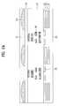
- FIG. 1is a cross-sectional diagram of a CMOS image sensor according to a related art.
- a first epitaxial layer(not shown) is grown on a semiconductor substrate 10 .
- a red photodiode 11is formed on the first epitaxial layer.
- a second epitaxial layer(not shown) is grown on the first epitaxial layer including the red photodiode 11 .
- a green photodiode 13is formed on the second epitaxial layer.
- a third epitaxial layer(not shown) is grown on the second epitaxial layer including the green photodiode 13 .
- a blue photodiode 15is formed on the third epitaxial layer.
- a trench for field isolationis formed on the third epitaxial layer.
- An STI (shallow trench isolation) layer 16is then formed by filling the trench with insulator.
- An insulating interlayer 17is formed on the third epitaxial layer.
- a first metal layer(not shown) is formed on the insulating interlayer 17 , and metal lines 23 are then formed by patterning the first metal layer. The process of forming the insulating interlayer 17 and the metal lines 23 is repeated several times to stack necessary metal lines 23 .
- a device protecting layer 20which may be made of nitride, is formed on the stacked insulating interlayer 17 to protect a device from moisture or physical shock.
- a microlens 22is then formed on the device protecting layer 20 .
- CMOS image sensorIn fabricating the CMOS image sensor according to the related art, if the metal line lies on a path of light having passed through the microlens 22 , diffused reflection is caused and degrades image quality.
- the related art methodhas the following problem. Since the device isolation layer, which may be nitride, is formed between the microlenses and is transparent, the diffused reflection degrades the image quality when the metal line lies in a path of the incident light via the device isolation layer.
- the device isolation layerwhich may be nitride
- the present inventionis directed to a CMOS image sensor and fabricating method thereof that substantially obviate one or more problems due to limitations and disadvantages of the related art.
- An advantage of the present inventionis to provide a CMOS image sensor and fabricating method thereof, by which the quality of the image sensor can be enhanced by preventing unnecessary diffused reflection of light by providing an opaque filter layer next to a microlens.
- a CMOS image sensorincludes a photodiode in a semiconductor substrate, an insulating interlayer on the semiconductor substrate including the photodiode, a metal line embedded within the insulating interlayer, a device protecting layer on the insulating interlayer, a microlens on the device protecting layer, wherein the microlens overlaps the photodiode, and an opaque layer pattern on the device protecting layer adjacent the microlens.
- a method of fabricating a CMOS image sensorincludes the steps of forming a photodiode in a semiconductor substrate, forming a first insulating interlayer on the semiconductor substrate including the photodiode, forming a metal line on the first insulating interlayer, forming a second insulating interlayer on the first insulating interlayer including the metal line, forming a device protecting layer on the second insulating interlayer, forming a microlens on the device protecting layer to be overlapped with the photodiode, and forming an opaque layer pattern on the device protecting layer adjacent the microlens.
- FIG. 1is a cross-sectional diagram of a CMOS image sensor according to a related art.
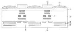
- FIG. 2A and FIG. 2Bare cross-sectional diagrams of a CMOS image sensor fabricated by a method of fabricating a CMOS image sensor according to the present invention.
- a first epitaxial layer(not shown) is grown on a semiconductor substrate 30 .
- a red photodiode 31is formed on the first epitaxial layer.
- a second epitaxial layer(not shown) is grown on the first epitaxial layer including the red photodiode 31 .
- a green photodiode 33is formed on the second epitaxial layer.
- a third epitaxial layer(not shown) is grown on the second epitaxial layer including the green photodiode 33 .
- a blue photodiode 35is formed on the third epitaxial layer.
- a trench for field isolationis formed on the third epitaxial layer.
- An STI (shallow trench isolation) layer 36is then formed by filling the trench with insulator.
- An insulating interlayer 47is formed on the third epitaxial layer including the blue photodiode 35 and the STI layer 36 .
- a first metal layer(not shown) is formed on the insulating interlayer 47 , and metal lines 46 are then formed by patterning the first metal layer. The process of forming the insulating interlayer 47 and the metal lines 46 is repeated several times to stack necessary metal lines 46 .
- the metal lines 46should be formed on the insulating interlayer to not be overlapped with the photodiodes 31 , 33 and 35 . Hence, light incident on the photodiodes 31 , 33 and 35 is not affected by the metal lines 46 .
- a device protecting layer 40which may be nitride, is formed on the stacked insulating interlayer 47 to protect a device from moisture or physical shock.
- the device protecting layer 40may then be planarized by chemical mechanical polishing (CMP).
- a photoresist layer(not shown) is coated on the planarized device protecting layer 40 . Exposure and development are performed on the photoresist layer to form a microlens pattern (not shown) on the device protecting layer 40 that overlaps with the photodiodes. Reflowing is performed on the microlens pattern by annealing to form hemispherical microlenses 50 .
- an opaque layer 51is formed on the device isolation layer 40 including the microlens 50 .
- the opaque layer 51is patterned to form an opaque layer pattern 52 remaining on the device protecting layer 40 overlapped with the metal lines 46 .
- the present inventionprovides the following effect.
- the opaque layer pattern between the microlensesi.e., on the device protecting layer overlapped with the metal lines
- light interference generated from deffused reflection, caused by light reflected by the metal lines via the microlenscan be eliminated.
- the image quality of the devicecan be enhanced.
Landscapes
- Solid State Image Pick-Up Elements (AREA)
Abstract
Description
- This application claims the benefit of Korean Patent Application No. 10-2004-0117182, filed on Dec. 30, 2004, which is hereby incorporated by reference for all purposes as if fully set forth herein.
- 1. Field of the Invention
- The present invention relates to a CMOS image sensor and a fabricating method thereof. Although the present invention is suitable for a wide scope of applications, it is particularly suitable for preventing diffused reflection that occurs due to the presence of metal lines by providing an opaque layer on a device isolation layer between microlenses.
- 2. Discussion of the Related Art
- Generally, an image sensor is a semiconductor device that converts an optic image to an electric signal. In a CCD (charge coupled device) image sensor, a plurality of MOS (metal-oxide-metal) capacitors are arranged close to one another to transfer and store electric charge carriers. In a CMOS (complementary MOS) image sensor, a plurality of MOS transistors corresponding to the number of pixels are fabricated by the CMOS technology using a control circuit and a signal processing circuit as peripheral circuits. Also, a switching system of sequentially detecting outputs using the MOS transistors is adopted.
- The CMOS image sensor converts image information of a subject to an electric signal by using signal processing chips including photodiodes. Since an amplifier, an analog/digital (A/D) converter, an internal voltage generator, a timing generator, a digital logic, etc. can be integrated on each of the chips, the CMOS image sensor is advantageous in saving space, power and cost. Moreover, mass production of CMOS image sensors is enabled through a silicon wafer etching process that is cheaper than the fabricating process for CCDs, which includes a more complex process.
- Thus, the CMOS image sensor has expanded into application fields such as digital cameras, smart phones, PDAs, notebook computers, security cameras, barcode detectors, toys, etc.
- To increase the photosensitivity of the CMOS image sensor, many efforts have been made to increase the fill factor, which indicates a rate of number of pixels of a pixel area within a chip. However, a logic circuit part for signal processing takes up space and therefore limits the fill factor. Hence, a microlens forming technology has been introduced to increase the photosensitivity. A microlens condenses light by diverting a path of the light incident on an area that does not include a photosensing device, such as a photodiode.
- An image of a subject may be transferred to the photodiode via the microlens. If a metal line within a device is in the way of a light path, diffused reflection occurs, which degrades image quality.
- A method of fabricating a CMOS image sensor according to the related art is explained with reference to the attached drawing as follows.
FIG. 1 is a cross-sectional diagram of a CMOS image sensor according to a related art. Referring toFIG. 1 , a first epitaxial layer (not shown) is grown on asemiconductor substrate 10. Ared photodiode 11 is formed on the first epitaxial layer. A second epitaxial layer (not shown) is grown on the first epitaxial layer including thered photodiode 11. Agreen photodiode 13 is formed on the second epitaxial layer. A third epitaxial layer (not shown) is grown on the second epitaxial layer including thegreen photodiode 13. Ablue photodiode 15 is formed on the third epitaxial layer. A trench for field isolation is formed on the third epitaxial layer. An STI (shallow trench isolation)layer 16 is then formed by filling the trench with insulator.- An
insulating interlayer 17 is formed on the third epitaxial layer. A first metal layer (not shown) is formed on theinsulating interlayer 17, andmetal lines 23 are then formed by patterning the first metal layer. The process of forming theinsulating interlayer 17 and themetal lines 23 is repeated several times to stacknecessary metal lines 23. Adevice protecting layer 20, which may be made of nitride, is formed on the stackedinsulating interlayer 17 to protect a device from moisture or physical shock. Amicrolens 22 is then formed on thedevice protecting layer 20. - In fabricating the CMOS image sensor according to the related art, if the metal line lies on a path of light having passed through the
microlens 22, diffused reflection is caused and degrades image quality. - The related art method has the following problem. Since the device isolation layer, which may be nitride, is formed between the microlenses and is transparent, the diffused reflection degrades the image quality when the metal line lies in a path of the incident light via the device isolation layer.
- Accordingly, the present invention is directed to a CMOS image sensor and fabricating method thereof that substantially obviate one or more problems due to limitations and disadvantages of the related art.
- An advantage of the present invention is to provide a CMOS image sensor and fabricating method thereof, by which the quality of the image sensor can be enhanced by preventing unnecessary diffused reflection of light by providing an opaque filter layer next to a microlens.
- Additional features and advantages of the invention will be set forth in the description which follows, and will be apparent from the description, or may be learned by practice of the invention. The objectives and other advantages of the invention will be realized and attained by the structure and method particularly pointed out in the written description and claims hereof as well as the appended drawings.
- To achieve these and other advantages and in accordance with the purpose of the present invention, as embodied and broadly described, a CMOS image sensor includes a photodiode in a semiconductor substrate, an insulating interlayer on the semiconductor substrate including the photodiode, a metal line embedded within the insulating interlayer, a device protecting layer on the insulating interlayer, a microlens on the device protecting layer, wherein the microlens overlaps the photodiode, and an opaque layer pattern on the device protecting layer adjacent the microlens.
- In another aspect of the present invention, a method of fabricating a CMOS image sensor includes the steps of forming a photodiode in a semiconductor substrate, forming a first insulating interlayer on the semiconductor substrate including the photodiode, forming a metal line on the first insulating interlayer, forming a second insulating interlayer on the first insulating interlayer including the metal line, forming a device protecting layer on the second insulating interlayer, forming a microlens on the device protecting layer to be overlapped with the photodiode, and forming an opaque layer pattern on the device protecting layer adjacent the microlens.
- It is to be understood that both the foregoing general description and the following detailed description are exemplary and explanatory and are intended to provide further explanation of the invention as claimed.
- The accompanying drawings, which are included to provide a further understanding of the invention and are incorporated in and constitute a part of this specification, illustrate exemplary embodiment(s) of the invention and together with the description serve to explain the principle of the invention. In the drawings:
FIG. 1 is a cross-sectional diagram of a CMOS image sensor according to a related art; andFIG. 2A andFIG. 2B are cross-sectional diagrams of a CMOS image sensor fabricated by a method of fabricating a CMOS image sensor according to the present invention.- Reference will now be made in detail to exemplary embodiments of the present invention, examples of which are illustrated in the accompanying drawings. Wherever possible, the same reference numbers will be used throughout the drawings to refer to the same or similar parts.
- Referring to
FIG. 2 , a first epitaxial layer (not shown) is grown on asemiconductor substrate 30. Ared photodiode 31 is formed on the first epitaxial layer. A second epitaxial layer (not shown) is grown on the first epitaxial layer including thered photodiode 31. Agreen photodiode 33 is formed on the second epitaxial layer. A third epitaxial layer (not shown) is grown on the second epitaxial layer including thegreen photodiode 33. Ablue photodiode 35 is formed on the third epitaxial layer. A trench for field isolation is formed on the third epitaxial layer. An STI (shallow trench isolation)layer 36 is then formed by filling the trench with insulator. - An insulating
interlayer 47 is formed on the third epitaxial layer including theblue photodiode 35 and theSTI layer 36. A first metal layer (not shown) is formed on the insulatinginterlayer 47, andmetal lines 46 are then formed by patterning the first metal layer. The process of forming the insulatinginterlayer 47 and themetal lines 46 is repeated several times to stack necessary metal lines46. Themetal lines 46 should be formed on the insulating interlayer to not be overlapped with thephotodiodes photodiodes - A
device protecting layer 40, which may be nitride, is formed on the stacked insulatinginterlayer 47 to protect a device from moisture or physical shock. Thedevice protecting layer 40 may then be planarized by chemical mechanical polishing (CMP). - A photoresist layer (not shown) is coated on the planarized
device protecting layer 40. Exposure and development are performed on the photoresist layer to form a microlens pattern (not shown) on thedevice protecting layer 40 that overlaps with the photodiodes. Reflowing is performed on the microlens pattern by annealing to formhemispherical microlenses 50. - Then, an
opaque layer 51 is formed on thedevice isolation layer 40 including themicrolens 50. - Referring to
FIG. 2B , theopaque layer 51 is patterned to form anopaque layer pattern 52 remaining on thedevice protecting layer 40 overlapped with the metal lines46. - Accordingly, the present invention provides the following effect.
- By providing the opaque layer pattern between the microlenses, i.e., on the device protecting layer overlapped with the metal lines, light interference generated from deffused reflection, caused by light reflected by the metal lines via the microlens, can be eliminated. Hence, the image quality of the device can be enhanced.
- It will be apparent to those skilled in the art that various modifications and variations can be made in the present invention without departing from the spirit or scope of the invention. Thus, it is intended that the present invention cover the modifications and variations of this invention provided they come within the scope of the appended claims and their equivalents.
Claims (10)
Applications Claiming Priority (2)
| Application Number | Priority Date | Filing Date | Title |
|---|---|---|---|
| KR10-2004-0117182 | 2004-12-30 | ||
| KR1020040117182AKR100660320B1 (en) | 2004-12-30 | 2004-12-30 | CMOS image sensor and its manufacturing method |
Publications (2)
| Publication Number | Publication Date |
|---|---|
| US20060145176A1true US20060145176A1 (en) | 2006-07-06 |
| US7705378B2 US7705378B2 (en) | 2010-04-27 |
Family
ID=36639368
Family Applications (1)
| Application Number | Title | Priority Date | Filing Date |
|---|---|---|---|
| US11/319,590Active - Reinstated2027-12-20US7705378B2 (en) | 2004-12-30 | 2005-12-29 | CMOS image sensor and fabricating method thereof |
Country Status (2)
| Country | Link |
|---|---|
| US (1) | US7705378B2 (en) |
| KR (1) | KR100660320B1 (en) |
Cited By (19)
| Publication number | Priority date | Publication date | Assignee | Title |
|---|---|---|---|---|
| US20090200626A1 (en)* | 2008-02-08 | 2009-08-13 | Omnivision Technologies Inc. | Backside illuminated imaging sensor with vertical pixel sensor |
| US20090218606A1 (en)* | 2008-02-29 | 2009-09-03 | Mccaffrey Nathaniel J | Vertically integrated light sensor and arrays |
| US20090218493A1 (en)* | 2008-02-29 | 2009-09-03 | Mccaffrey Nathaniel J | Wide spectral range hybrid image detector |
| US20100078636A1 (en)* | 2007-02-20 | 2010-04-01 | Nxp, B.V. | Semiconductor device with backside tamper protection |
| US20100244173A1 (en)* | 2009-03-30 | 2010-09-30 | Taiwan Semiconductor Manufacturing Company, Ltd. | Image sensor and method of fabricating same |
| US20110227138A1 (en)* | 2009-09-17 | 2011-09-22 | Homayoon Haddad | Photosensitive Imaging Devices And Associated Methods |
| US9029785B2 (en) | 2011-03-03 | 2015-05-12 | Samsung Electronics Co., Ltd. | Method of fabricating microlens, and depth sensor including microlens |
| US9496308B2 (en) | 2011-06-09 | 2016-11-15 | Sionyx, Llc | Process module for increasing the response of backside illuminated photosensitive imagers and associated methods |
| US9673250B2 (en) | 2013-06-29 | 2017-06-06 | Sionyx, Llc | Shallow trench textured regions and associated methods |
| US9741761B2 (en) | 2010-04-21 | 2017-08-22 | Sionyx, Llc | Photosensitive imaging devices and associated methods |
| US9762830B2 (en) | 2013-02-15 | 2017-09-12 | Sionyx, Llc | High dynamic range CMOS image sensor having anti-blooming properties and associated methods |
| US9761739B2 (en) | 2010-06-18 | 2017-09-12 | Sionyx, Llc | High speed photosensitive devices and associated methods |
| US9905599B2 (en) | 2012-03-22 | 2018-02-27 | Sionyx, Llc | Pixel isolation elements, devices and associated methods |
| US9911781B2 (en) | 2009-09-17 | 2018-03-06 | Sionyx, Llc | Photosensitive imaging devices and associated methods |
| US9939251B2 (en) | 2013-03-15 | 2018-04-10 | Sionyx, Llc | Three dimensional imaging utilizing stacked imager devices and associated methods |
| US10244188B2 (en) | 2011-07-13 | 2019-03-26 | Sionyx, Llc | Biometric imaging devices and associated methods |
| US10361232B2 (en) | 2009-09-17 | 2019-07-23 | Sionyx, Llc | Photosensitive imaging devices and associated methods |
| US10374109B2 (en) | 2001-05-25 | 2019-08-06 | President And Fellows Of Harvard College | Silicon-based visible and near-infrared optoelectric devices |
| US10741399B2 (en) | 2004-09-24 | 2020-08-11 | President And Fellows Of Harvard College | Femtosecond laser-induced formation of submicrometer spikes on a semiconductor substrate |
Families Citing this family (1)
| Publication number | Priority date | Publication date | Assignee | Title |
|---|---|---|---|---|
| KR100958628B1 (en)* | 2007-12-27 | 2010-05-19 | 주식회사 동부하이텍 | Manufacturing Method of CMOS Image Sensor |
Citations (7)
| Publication number | Priority date | Publication date | Assignee | Title |
|---|---|---|---|---|
| US5396090A (en)* | 1993-02-17 | 1995-03-07 | Sharp Kabushiki Kaisha | Solid state imaging device having partition wall for partitioning bottom portions of micro lenses |
| US6379992B2 (en)* | 1999-12-28 | 2002-04-30 | Hynix Semiconductor Inc. | Method for fabricating an image sensor |
| US6414343B1 (en)* | 1999-10-07 | 2002-07-02 | Fuji Photo Film., Ltd. | Solid-state imaging device having aspheric lenses |
| US6632701B2 (en)* | 2000-09-25 | 2003-10-14 | Foveon, Inc. | Vertical color filter detector group and array |
| US20060043515A1 (en)* | 2004-08-25 | 2006-03-02 | Loriston Ford | Light block for pixel arrays |
| US20060054939A1 (en)* | 2004-09-14 | 2006-03-16 | Tzu-Hsuan Hsu | CMOS image sensor |
| US20060086957A1 (en)* | 2004-10-27 | 2006-04-27 | Samsung Electronics Co.; Ltd | CMOS image sensor using reflection grating and method for manufacturing the same |
Family Cites Families (1)
| Publication number | Priority date | Publication date | Assignee | Title |
|---|---|---|---|---|
| KR0165376B1 (en) | 1995-03-31 | 1998-12-15 | 김광호 | CD image sensor and its manufacturing method |
- 2004
- 2004-12-30KRKR1020040117182Apatent/KR100660320B1/ennot_activeExpired - Fee Related
- 2005
- 2005-12-29USUS11/319,590patent/US7705378B2/enactiveActive - Reinstated
Patent Citations (7)
| Publication number | Priority date | Publication date | Assignee | Title |
|---|---|---|---|---|
| US5396090A (en)* | 1993-02-17 | 1995-03-07 | Sharp Kabushiki Kaisha | Solid state imaging device having partition wall for partitioning bottom portions of micro lenses |
| US6414343B1 (en)* | 1999-10-07 | 2002-07-02 | Fuji Photo Film., Ltd. | Solid-state imaging device having aspheric lenses |
| US6379992B2 (en)* | 1999-12-28 | 2002-04-30 | Hynix Semiconductor Inc. | Method for fabricating an image sensor |
| US6632701B2 (en)* | 2000-09-25 | 2003-10-14 | Foveon, Inc. | Vertical color filter detector group and array |
| US20060043515A1 (en)* | 2004-08-25 | 2006-03-02 | Loriston Ford | Light block for pixel arrays |
| US20060054939A1 (en)* | 2004-09-14 | 2006-03-16 | Tzu-Hsuan Hsu | CMOS image sensor |
| US20060086957A1 (en)* | 2004-10-27 | 2006-04-27 | Samsung Electronics Co.; Ltd | CMOS image sensor using reflection grating and method for manufacturing the same |
Cited By (32)
| Publication number | Priority date | Publication date | Assignee | Title |
|---|---|---|---|---|
| US10374109B2 (en) | 2001-05-25 | 2019-08-06 | President And Fellows Of Harvard College | Silicon-based visible and near-infrared optoelectric devices |
| US10741399B2 (en) | 2004-09-24 | 2020-08-11 | President And Fellows Of Harvard College | Femtosecond laser-induced formation of submicrometer spikes on a semiconductor substrate |
| US8198641B2 (en)* | 2007-02-20 | 2012-06-12 | Nxp B.V. | Semiconductor device with backside tamper protection |
| US20100078636A1 (en)* | 2007-02-20 | 2010-04-01 | Nxp, B.V. | Semiconductor device with backside tamper protection |
| US8063465B2 (en)* | 2008-02-08 | 2011-11-22 | Omnivision Technologies, Inc. | Backside illuminated imaging sensor with vertical pixel sensor |
| US8513762B2 (en) | 2008-02-08 | 2013-08-20 | Omnivision Technologies, Inc. | Backside illuminated imaging sensor with vertical pixel sensor |
| US20090200626A1 (en)* | 2008-02-08 | 2009-08-13 | Omnivision Technologies Inc. | Backside illuminated imaging sensor with vertical pixel sensor |
| US20090218493A1 (en)* | 2008-02-29 | 2009-09-03 | Mccaffrey Nathaniel J | Wide spectral range hybrid image detector |
| US8058615B2 (en) | 2008-02-29 | 2011-11-15 | Sionyx, Inc. | Wide spectral range hybrid image detector |
| US20090218606A1 (en)* | 2008-02-29 | 2009-09-03 | Mccaffrey Nathaniel J | Vertically integrated light sensor and arrays |
| US8227288B2 (en)* | 2009-03-30 | 2012-07-24 | Taiwan Semiconductor Manufacturing Company, Ltd. | Image sensor and method of fabricating same |
| US20100244173A1 (en)* | 2009-03-30 | 2010-09-30 | Taiwan Semiconductor Manufacturing Company, Ltd. | Image sensor and method of fabricating same |
| US20110227138A1 (en)* | 2009-09-17 | 2011-09-22 | Homayoon Haddad | Photosensitive Imaging Devices And Associated Methods |
| US8680591B2 (en) | 2009-09-17 | 2014-03-25 | Sionyx, Inc. | Photosensitive imaging devices and associated methods |
| US10361232B2 (en) | 2009-09-17 | 2019-07-23 | Sionyx, Llc | Photosensitive imaging devices and associated methods |
| US9911781B2 (en) | 2009-09-17 | 2018-03-06 | Sionyx, Llc | Photosensitive imaging devices and associated methods |
| US9741761B2 (en) | 2010-04-21 | 2017-08-22 | Sionyx, Llc | Photosensitive imaging devices and associated methods |
| US10229951B2 (en) | 2010-04-21 | 2019-03-12 | Sionyx, Llc | Photosensitive imaging devices and associated methods |
| US10505054B2 (en) | 2010-06-18 | 2019-12-10 | Sionyx, Llc | High speed photosensitive devices and associated methods |
| US9761739B2 (en) | 2010-06-18 | 2017-09-12 | Sionyx, Llc | High speed photosensitive devices and associated methods |
| US9029785B2 (en) | 2011-03-03 | 2015-05-12 | Samsung Electronics Co., Ltd. | Method of fabricating microlens, and depth sensor including microlens |
| US10269861B2 (en) | 2011-06-09 | 2019-04-23 | Sionyx, Llc | Process module for increasing the response of backside illuminated photosensitive imagers and associated methods |
| US9666636B2 (en) | 2011-06-09 | 2017-05-30 | Sionyx, Llc | Process module for increasing the response of backside illuminated photosensitive imagers and associated methods |
| US9496308B2 (en) | 2011-06-09 | 2016-11-15 | Sionyx, Llc | Process module for increasing the response of backside illuminated photosensitive imagers and associated methods |
| US10244188B2 (en) | 2011-07-13 | 2019-03-26 | Sionyx, Llc | Biometric imaging devices and associated methods |
| US9905599B2 (en) | 2012-03-22 | 2018-02-27 | Sionyx, Llc | Pixel isolation elements, devices and associated methods |
| US10224359B2 (en) | 2012-03-22 | 2019-03-05 | Sionyx, Llc | Pixel isolation elements, devices and associated methods |
| US9762830B2 (en) | 2013-02-15 | 2017-09-12 | Sionyx, Llc | High dynamic range CMOS image sensor having anti-blooming properties and associated methods |
| US9939251B2 (en) | 2013-03-15 | 2018-04-10 | Sionyx, Llc | Three dimensional imaging utilizing stacked imager devices and associated methods |
| US9673250B2 (en) | 2013-06-29 | 2017-06-06 | Sionyx, Llc | Shallow trench textured regions and associated methods |
| US10347682B2 (en) | 2013-06-29 | 2019-07-09 | Sionyx, Llc | Shallow trench textured regions and associated methods |
| US11069737B2 (en) | 2013-06-29 | 2021-07-20 | Sionyx, Llc | Shallow trench textured regions and associated methods |
Also Published As
| Publication number | Publication date |
|---|---|
| KR20060077670A (en) | 2006-07-05 |
| US7705378B2 (en) | 2010-04-27 |
| KR100660320B1 (en) | 2006-12-22 |
Similar Documents
| Publication | Publication Date | Title |
|---|---|---|
| US7705378B2 (en) | CMOS image sensor and fabricating method thereof | |
| US11843015B2 (en) | Image sensors | |
| US7683451B2 (en) | CMOS image sensors with light shielding patterns | |
| KR100660319B1 (en) | CMOS image sensor and manufacturing method | |
| US7262448B2 (en) | CMOS image sensor | |
| US20090108310A1 (en) | CMOS image sensor and fabricating method thereof | |
| US20060145218A1 (en) | Microlens of CMOS image sensor and method of manufacturing the same | |
| KR100544018B1 (en) | CMOS image sensor with photodiode extended at the back of wafer and its manufacturing method | |
| US20070246757A1 (en) | CMOS image sensor and method for fabricating the same | |
| KR100672698B1 (en) | CMOS image sensor and its manufacturing method | |
| US7378295B2 (en) | CMOS image sensor and fabricating method thereof | |
| US7442975B2 (en) | CMOS image sensor and method for fabricating the same | |
| US7439095B2 (en) | CMOS image sensor and method for fabricating the same | |
| KR100649010B1 (en) | CMOS image sensor and its manufacturing method | |
| KR20060076430A (en) | Light shielding film of CMOS image sensor and its formation method | |
| KR100989987B1 (en) | Manufacturing method of CMOS image sensor preventing the peeling phenomenon of overcoating layer | |
| KR20040058749A (en) | CMOS image sensor with microlense having different radius of curvature comparing to wavelength of incident light and the method of fabricating the same | |
| KR100741914B1 (en) | Manufacturing Method of CMOS Image Sensor | |
| KR100884485B1 (en) | CMOS image sensor with light blocking film and manufacturing method thereof | |
| US20060145278A1 (en) | CMOS image sensor and method for manufacturing the same | |
| KR20050106932A (en) | Image sensor and fabricating method thereof | |
| US20080157134A1 (en) | Cmos image sensor and fabricating method thereof | |
| KR100824625B1 (en) | CMOS image sensor and its manufacturing method | |
| KR20070081702A (en) | Image sensor and its formation method | |
| KR20060077535A (en) | CMOS image sensor and its manufacturing method |
Legal Events
| Date | Code | Title | Description |
|---|---|---|---|
| AS | Assignment | Owner name:DONGBUANAM SEMICONDUCTOR INC.,KOREA, REPUBLIC OF Free format text:ASSIGNMENT OF ASSIGNORS INTEREST;ASSIGNOR:LEE, CHANG EUN;REEL/FRAME:017387/0817 Effective date:20051229 Owner name:DONGBUANAM SEMICONDUCTOR INC., KOREA, REPUBLIC OF Free format text:ASSIGNMENT OF ASSIGNORS INTEREST;ASSIGNOR:LEE, CHANG EUN;REEL/FRAME:017387/0817 Effective date:20051229 | |
| AS | Assignment | Owner name:DONGBU ELECTRONICS CO., LTD.,KOREA, REPUBLIC OF Free format text:CHANGE OF NAME;ASSIGNOR:DONGBUANAM SEMICONDUCTOR INC.;REEL/FRAME:018176/0351 Effective date:20060324 | |
| FEPP | Fee payment procedure | Free format text:PAYOR NUMBER ASSIGNED (ORIGINAL EVENT CODE: ASPN); ENTITY STATUS OF PATENT OWNER: LARGE ENTITY | |
| STCF | Information on status: patent grant | Free format text:PATENTED CASE | |
| FEPP | Fee payment procedure | Free format text:PETITION RELATED TO MAINTENANCE FEES GRANTED (ORIGINAL EVENT CODE: PMFG); ENTITY STATUS OF PATENT OWNER: LARGE ENTITY Free format text:PETITION RELATED TO MAINTENANCE FEES FILED (ORIGINAL EVENT CODE: PMFP); ENTITY STATUS OF PATENT OWNER: LARGE ENTITY | |
| REMI | Maintenance fee reminder mailed | ||
| PRDP | Patent reinstated due to the acceptance of a late maintenance fee | Effective date:20140516 | |
| FPAY | Fee payment | Year of fee payment:4 | |
| SULP | Surcharge for late payment | ||
| FEPP | Fee payment procedure | Free format text:PAYOR NUMBER ASSIGNED (ORIGINAL EVENT CODE: ASPN); ENTITY STATUS OF PATENT OWNER: LARGE ENTITY Free format text:PAYER NUMBER DE-ASSIGNED (ORIGINAL EVENT CODE: RMPN); ENTITY STATUS OF PATENT OWNER: LARGE ENTITY | |
| AS | Assignment | Owner name:III HOLDINGS 4, LLC, DELAWARE Free format text:ASSIGNMENT OF ASSIGNORS INTEREST;ASSIGNOR:DONGBU ELECTRONICS CO., LTD.;REEL/FRAME:035383/0560 Effective date:20150129 | |
| MAFP | Maintenance fee payment | Free format text:PAYMENT OF MAINTENANCE FEE, 8TH YEAR, LARGE ENTITY (ORIGINAL EVENT CODE: M1552) Year of fee payment:8 | |
| MAFP | Maintenance fee payment | Free format text:PAYMENT OF MAINTENANCE FEE, 12TH YEAR, LARGE ENTITY (ORIGINAL EVENT CODE: M1553); ENTITY STATUS OF PATENT OWNER: LARGE ENTITY Year of fee payment:12 |