US20060130767A1 - Purged vacuum chuck with proximity pins - Google Patents
Purged vacuum chuck with proximity pinsDownload PDFInfo
- Publication number
- US20060130767A1 US20060130767A1US11/111,155US11115505AUS2006130767A1US 20060130767 A1US20060130767 A1US 20060130767A1US 11115505 AUS11115505 AUS 11115505AUS 2006130767 A1US2006130767 A1US 2006130767A1
- Authority
- US
- United States
- Prior art keywords
- substrate support
- substrate
- plate
- recessed regions
- proximity pins
- Prior art date
- Legal status (The legal status is an assumption and is not a legal conclusion. Google has not performed a legal analysis and makes no representation as to the accuracy of the status listed.)
- Abandoned
Links
- 239000000758substrateSubstances0.000claimsabstractdescription148
- 238000010926purgeMethods0.000claimsabstractdescription16
- 238000000034methodMethods0.000claimsdescription80
- 239000000463materialSubstances0.000claimsdescription46
- 230000008569processEffects0.000claimsdescription36
- 239000013078crystalSubstances0.000claimsdescription20
- 238000004519manufacturing processMethods0.000claimsdescription20
- 125000006850spacer groupChemical group0.000claimsdescription20
- 229910052594sapphireInorganic materials0.000claimsdescription18
- 239000010980sapphireSubstances0.000claimsdescription18
- 229910052782aluminiumInorganic materials0.000claimsdescription17
- XAGFODPZIPBFFR-UHFFFAOYSA-NaluminiumChemical compound[Al]XAGFODPZIPBFFR-UHFFFAOYSA-N0.000claimsdescription17
- 229910052582BNInorganic materials0.000claimsdescription11
- PZNSFCLAULLKQX-UHFFFAOYSA-NBoron nitrideChemical compoundN#BPZNSFCLAULLKQX-UHFFFAOYSA-N0.000claimsdescription11
- VYPSYNLAJGMNEJ-UHFFFAOYSA-NSilicium dioxideChemical compoundO=[Si]=OVYPSYNLAJGMNEJ-UHFFFAOYSA-N0.000claimsdescription10
- OKTJSMMVPCPJKN-UHFFFAOYSA-NCarbonChemical compound[C]OKTJSMMVPCPJKN-UHFFFAOYSA-N0.000claimsdescription9
- XUIMIQQOPSSXEZ-UHFFFAOYSA-NSiliconChemical compound[Si]XUIMIQQOPSSXEZ-UHFFFAOYSA-N0.000claimsdescription9
- 238000000151depositionMethods0.000claimsdescription9
- 229910052710siliconInorganic materials0.000claimsdescription9
- 239000010703siliconSubstances0.000claimsdescription9
- HBMJWWWQQXIZIP-UHFFFAOYSA-Nsilicon carbideChemical compound[Si+]#[C-]HBMJWWWQQXIZIP-UHFFFAOYSA-N0.000claimsdescription9
- 229910010271silicon carbideInorganic materials0.000claimsdescription9
- 229910003460diamondInorganic materials0.000claimsdescription8
- 239000010432diamondSubstances0.000claimsdescription8
- TWNQGVIAIRXVLR-UHFFFAOYSA-Noxo(oxoalumanyloxy)alumaneChemical compoundO=[Al]O[Al]=OTWNQGVIAIRXVLR-UHFFFAOYSA-N0.000claimsdescription7
- RYGMFSIKBFXOCR-UHFFFAOYSA-NCopperChemical compound[Cu]RYGMFSIKBFXOCR-UHFFFAOYSA-N0.000claimsdescription6
- 229910052802copperInorganic materials0.000claimsdescription6
- 239000010949copperSubstances0.000claimsdescription6
- PMHQVHHXPFUNSP-UHFFFAOYSA-Mcopper(1+);methylsulfanylmethane;bromideChemical compoundBr[Cu].CSCPMHQVHHXPFUNSP-UHFFFAOYSA-M0.000claimsdescription6
- 229910002804graphiteInorganic materials0.000claimsdescription6
- 239000010439graphiteSubstances0.000claimsdescription6
- 229920000642polymerPolymers0.000claimsdescription5
- 229910001220stainless steelInorganic materials0.000claimsdescription5
- 239000010935stainless steelSubstances0.000claimsdescription5
- 238000003825pressingMethods0.000claimsdescription4
- 229910052799carbonInorganic materials0.000claimsdescription3
- 229910052751metalInorganic materials0.000claimsdescription3
- 239000002184metalSubstances0.000claimsdescription3
- 229910052814silicon oxideInorganic materials0.000claimsdescription3
- PNEYBMLMFCGWSK-UHFFFAOYSA-NAluminaChemical compound[O-2].[O-2].[O-2].[Al+3].[Al+3]PNEYBMLMFCGWSK-UHFFFAOYSA-N0.000claims1
- 229910000873Beta-alumina solid electrolyteInorganic materials0.000claims1
- 239000000919ceramicSubstances0.000claims1
- 150000002739metalsChemical class0.000claims1
- LIVNPJMFVYWSIS-UHFFFAOYSA-Nsilicon monoxideChemical class[Si-]#[O+]LIVNPJMFVYWSIS-UHFFFAOYSA-N0.000claims1
- 239000010410layerSubstances0.000description28
- 239000007789gasSubstances0.000description25
- 238000012545processingMethods0.000description25
- 230000000873masking effectEffects0.000description16
- 239000004065semiconductorSubstances0.000description15
- 235000012431wafersNutrition0.000description13
- 230000015572biosynthetic processEffects0.000description10
- 230000008878couplingEffects0.000description10
- 238000010168coupling processMethods0.000description10
- 238000005859coupling reactionMethods0.000description10
- 238000005229chemical vapour depositionMethods0.000description9
- 238000005240physical vapour depositionMethods0.000description9
- 229920006362Teflon®Polymers0.000description8
- 239000002245particleSubstances0.000description7
- 230000008021depositionEffects0.000description6
- 238000012986modificationMethods0.000description6
- 230000004048modificationEffects0.000description6
- 230000008901benefitEffects0.000description5
- PXHVJJICTQNCMI-UHFFFAOYSA-NNickelChemical compound[Ni]PXHVJJICTQNCMI-UHFFFAOYSA-N0.000description4
- 238000005422blastingMethods0.000description4
- 230000003247decreasing effectEffects0.000description4
- 238000005137deposition processMethods0.000description4
- 230000007246mechanismEffects0.000description4
- 239000000377silicon dioxideSubstances0.000description4
- 238000012546transferMethods0.000description4
- 239000004642PolyimideSubstances0.000description3
- 238000000576coating methodMethods0.000description3
- 238000005530etchingMethods0.000description3
- 239000001307heliumSubstances0.000description3
- 229910052734heliumInorganic materials0.000description3
- SWQJXJOGLNCZEY-UHFFFAOYSA-Nhelium atomChemical compound[He]SWQJXJOGLNCZEY-UHFFFAOYSA-N0.000description3
- 238000000059patterningMethods0.000description3
- 229920001721polyimidePolymers0.000description3
- XKRFYHLGVUSROY-UHFFFAOYSA-NArgonChemical compound[Ar]XKRFYHLGVUSROY-UHFFFAOYSA-N0.000description2
- IJGRMHOSHXDMSA-UHFFFAOYSA-NAtomic nitrogenChemical compoundN#NIJGRMHOSHXDMSA-UHFFFAOYSA-N0.000description2
- ZOKXTWBITQBERF-UHFFFAOYSA-NMolybdenumChemical compound[Mo]ZOKXTWBITQBERF-UHFFFAOYSA-N0.000description2
- RTAQQCXQSZGOHL-UHFFFAOYSA-NTitaniumChemical compound[Ti]RTAQQCXQSZGOHL-UHFFFAOYSA-N0.000description2
- NRTOMJZYCJJWKI-UHFFFAOYSA-NTitanium nitrideChemical compound[Ti]#NNRTOMJZYCJJWKI-UHFFFAOYSA-N0.000description2
- 229910010293ceramic materialInorganic materials0.000description2
- 239000004020conductorSubstances0.000description2
- 239000000356contaminantSubstances0.000description2
- 238000007796conventional methodMethods0.000description2
- 238000001816coolingMethods0.000description2
- 230000007547defectEffects0.000description2
- 230000003993interactionEffects0.000description2
- VNWKTOKETHGBQD-UHFFFAOYSA-NmethaneChemical compoundCVNWKTOKETHGBQD-UHFFFAOYSA-N0.000description2
- 229910052750molybdenumInorganic materials0.000description2
- 239000011733molybdenumSubstances0.000description2
- 229910052759nickelInorganic materials0.000description2
- 230000009467reductionEffects0.000description2
- 235000012239silicon dioxideNutrition0.000description2
- 239000007787solidSubstances0.000description2
- 239000010936titaniumSubstances0.000description2
- 229910052719titaniumInorganic materials0.000description2
- WFKWXMTUELFFGS-UHFFFAOYSA-NtungstenChemical compound[W]WFKWXMTUELFFGS-UHFFFAOYSA-N0.000description2
- 229910052721tungstenInorganic materials0.000description2
- 239000010937tungstenSubstances0.000description2
- 229910006587β-Al2O3Inorganic materials0.000description2
- MYMOFIZGZYHOMD-UHFFFAOYSA-NDioxygenChemical compoundO=OMYMOFIZGZYHOMD-UHFFFAOYSA-N0.000description1
- 239000004593EpoxySubstances0.000description1
- UFHFLCQGNIYNRP-UHFFFAOYSA-NHydrogenChemical compound[H][H]UFHFLCQGNIYNRP-UHFFFAOYSA-N0.000description1
- 230000002411adverseEffects0.000description1
- 229910052786argonInorganic materials0.000description1
- 238000006243chemical reactionMethods0.000description1
- 239000011248coating agentSubstances0.000description1
- 239000011247coating layerSubstances0.000description1
- 238000004891communicationMethods0.000description1
- 230000001419dependent effectEffects0.000description1
- 238000009792diffusion processMethods0.000description1
- 238000009826distributionMethods0.000description1
- 238000000407epitaxyMethods0.000description1
- 238000001704evaporationMethods0.000description1
- 239000012530fluidSubstances0.000description1
- 239000001257hydrogenSubstances0.000description1
- 229910052739hydrogenInorganic materials0.000description1
- 239000011261inert gasSubstances0.000description1
- 229910052743kryptonInorganic materials0.000description1
- DNNSSWSSYDEUBZ-UHFFFAOYSA-Nkrypton atomChemical compound[Kr]DNNSSWSSYDEUBZ-UHFFFAOYSA-N0.000description1
- 238000000608laser ablationMethods0.000description1
- 238000003754machiningMethods0.000description1
- 238000005259measurementMethods0.000description1
- 229910052757nitrogenInorganic materials0.000description1
- 239000001301oxygenSubstances0.000description1
- 229910052760oxygenInorganic materials0.000description1
- 238000005268plasma chemical vapour depositionMethods0.000description1
- 239000002952polymeric resinSubstances0.000description1
- 229920001296polysiloxanePolymers0.000description1
- 239000002904solventSubstances0.000description1
- 238000000992sputter etchingMethods0.000description1
- -1such asSubstances0.000description1
- 229920003002synthetic resinPolymers0.000description1
- 125000000391vinyl groupChemical group[H]C([*])=C([H])[H]0.000description1
- 229920002554vinyl polymerPolymers0.000description1
- 229910052724xenonInorganic materials0.000description1
- FHNFHKCVQCLJFQ-UHFFFAOYSA-Nxenon atomChemical compound[Xe]FHNFHKCVQCLJFQ-UHFFFAOYSA-N0.000description1
Images


Classifications
- H—ELECTRICITY
- H01—ELECTRIC ELEMENTS
- H01L—SEMICONDUCTOR DEVICES NOT COVERED BY CLASS H10
- H01L21/00—Processes or apparatus adapted for the manufacture or treatment of semiconductor or solid state devices or of parts thereof
- H01L21/67—Apparatus specially adapted for handling semiconductor or electric solid state devices during manufacture or treatment thereof; Apparatus specially adapted for handling wafers during manufacture or treatment of semiconductor or electric solid state devices or components ; Apparatus not specifically provided for elsewhere
- H01L21/67005—Apparatus not specifically provided for elsewhere
- H01L21/67011—Apparatus for manufacture or treatment
- H01L21/67155—Apparatus for manufacturing or treating in a plurality of work-stations
- H01L21/67207—Apparatus for manufacturing or treating in a plurality of work-stations comprising a chamber adapted to a particular process
- H01L21/67225—Apparatus for manufacturing or treating in a plurality of work-stations comprising a chamber adapted to a particular process comprising at least one lithography chamber
- G—PHYSICS
- G03—PHOTOGRAPHY; CINEMATOGRAPHY; ANALOGOUS TECHNIQUES USING WAVES OTHER THAN OPTICAL WAVES; ELECTROGRAPHY; HOLOGRAPHY
- G03B—APPARATUS OR ARRANGEMENTS FOR TAKING PHOTOGRAPHS OR FOR PROJECTING OR VIEWING THEM; APPARATUS OR ARRANGEMENTS EMPLOYING ANALOGOUS TECHNIQUES USING WAVES OTHER THAN OPTICAL WAVES; ACCESSORIES THEREFOR
- G03B27/00—Photographic printing apparatus
- G03B27/32—Projection printing apparatus, e.g. enlarger, copying camera
- G—PHYSICS
- G03—PHOTOGRAPHY; CINEMATOGRAPHY; ANALOGOUS TECHNIQUES USING WAVES OTHER THAN OPTICAL WAVES; ELECTROGRAPHY; HOLOGRAPHY
- G03D—APPARATUS FOR PROCESSING EXPOSED PHOTOGRAPHIC MATERIALS; ACCESSORIES THEREFOR
- G03D13/00—Processing apparatus or accessories therefor, not covered by groups G11B3/00 - G11B11/00
- G03D13/006—Temperature control of the developer
- G—PHYSICS
- G03—PHOTOGRAPHY; CINEMATOGRAPHY; ANALOGOUS TECHNIQUES USING WAVES OTHER THAN OPTICAL WAVES; ELECTROGRAPHY; HOLOGRAPHY
- G03F—PHOTOMECHANICAL PRODUCTION OF TEXTURED OR PATTERNED SURFACES, e.g. FOR PRINTING, FOR PROCESSING OF SEMICONDUCTOR DEVICES; MATERIALS THEREFOR; ORIGINALS THEREFOR; APPARATUS SPECIALLY ADAPTED THEREFOR
- G03F7/00—Photomechanical, e.g. photolithographic, production of textured or patterned surfaces, e.g. printing surfaces; Materials therefor, e.g. comprising photoresists; Apparatus specially adapted therefor
- G03F7/26—Processing photosensitive materials; Apparatus therefor
- G03F7/40—Treatment after imagewise removal, e.g. baking
- G—PHYSICS
- G05—CONTROLLING; REGULATING
- G05B—CONTROL OR REGULATING SYSTEMS IN GENERAL; FUNCTIONAL ELEMENTS OF SUCH SYSTEMS; MONITORING OR TESTING ARRANGEMENTS FOR SUCH SYSTEMS OR ELEMENTS
- G05B19/00—Programme-control systems
- G05B19/02—Programme-control systems electric
- G05B19/418—Total factory control, i.e. centrally controlling a plurality of machines, e.g. direct or distributed numerical control [DNC], flexible manufacturing systems [FMS], integrated manufacturing systems [IMS] or computer integrated manufacturing [CIM]
- G05B19/41815—Total factory control, i.e. centrally controlling a plurality of machines, e.g. direct or distributed numerical control [DNC], flexible manufacturing systems [FMS], integrated manufacturing systems [IMS] or computer integrated manufacturing [CIM] characterised by the cooperation between machine tools, manipulators and conveyor or other workpiece supply system, workcell
- G05B19/41825—Total factory control, i.e. centrally controlling a plurality of machines, e.g. direct or distributed numerical control [DNC], flexible manufacturing systems [FMS], integrated manufacturing systems [IMS] or computer integrated manufacturing [CIM] characterised by the cooperation between machine tools, manipulators and conveyor or other workpiece supply system, workcell machine tools and manipulators only, machining centre
- H—ELECTRICITY
- H01—ELECTRIC ELEMENTS
- H01L—SEMICONDUCTOR DEVICES NOT COVERED BY CLASS H10
- H01L21/00—Processes or apparatus adapted for the manufacture or treatment of semiconductor or solid state devices or of parts thereof
- H01L21/67—Apparatus specially adapted for handling semiconductor or electric solid state devices during manufacture or treatment thereof; Apparatus specially adapted for handling wafers during manufacture or treatment of semiconductor or electric solid state devices or components ; Apparatus not specifically provided for elsewhere
- H01L21/67005—Apparatus not specifically provided for elsewhere
- H01L21/67011—Apparatus for manufacture or treatment
- H01L21/67098—Apparatus for thermal treatment
- H01L21/67109—Apparatus for thermal treatment mainly by convection
- H—ELECTRICITY
- H01—ELECTRIC ELEMENTS
- H01L—SEMICONDUCTOR DEVICES NOT COVERED BY CLASS H10
- H01L21/00—Processes or apparatus adapted for the manufacture or treatment of semiconductor or solid state devices or of parts thereof
- H01L21/67—Apparatus specially adapted for handling semiconductor or electric solid state devices during manufacture or treatment thereof; Apparatus specially adapted for handling wafers during manufacture or treatment of semiconductor or electric solid state devices or components ; Apparatus not specifically provided for elsewhere
- H01L21/67005—Apparatus not specifically provided for elsewhere
- H01L21/67011—Apparatus for manufacture or treatment
- H01L21/6715—Apparatus for applying a liquid, a resin, an ink or the like
- H—ELECTRICITY
- H01—ELECTRIC ELEMENTS
- H01L—SEMICONDUCTOR DEVICES NOT COVERED BY CLASS H10
- H01L21/00—Processes or apparatus adapted for the manufacture or treatment of semiconductor or solid state devices or of parts thereof
- H01L21/67—Apparatus specially adapted for handling semiconductor or electric solid state devices during manufacture or treatment thereof; Apparatus specially adapted for handling wafers during manufacture or treatment of semiconductor or electric solid state devices or components ; Apparatus not specifically provided for elsewhere
- H01L21/67005—Apparatus not specifically provided for elsewhere
- H01L21/67011—Apparatus for manufacture or treatment
- H01L21/67155—Apparatus for manufacturing or treating in a plurality of work-stations
- H01L21/67161—Apparatus for manufacturing or treating in a plurality of work-stations characterized by the layout of the process chambers
- H01L21/67173—Apparatus for manufacturing or treating in a plurality of work-stations characterized by the layout of the process chambers in-line arrangement
- H—ELECTRICITY
- H01—ELECTRIC ELEMENTS
- H01L—SEMICONDUCTOR DEVICES NOT COVERED BY CLASS H10
- H01L21/00—Processes or apparatus adapted for the manufacture or treatment of semiconductor or solid state devices or of parts thereof
- H01L21/67—Apparatus specially adapted for handling semiconductor or electric solid state devices during manufacture or treatment thereof; Apparatus specially adapted for handling wafers during manufacture or treatment of semiconductor or electric solid state devices or components ; Apparatus not specifically provided for elsewhere
- H01L21/67005—Apparatus not specifically provided for elsewhere
- H01L21/67011—Apparatus for manufacture or treatment
- H01L21/67155—Apparatus for manufacturing or treating in a plurality of work-stations
- H01L21/67161—Apparatus for manufacturing or treating in a plurality of work-stations characterized by the layout of the process chambers
- H01L21/67178—Apparatus for manufacturing or treating in a plurality of work-stations characterized by the layout of the process chambers vertical arrangement
- H—ELECTRICITY
- H01—ELECTRIC ELEMENTS
- H01L—SEMICONDUCTOR DEVICES NOT COVERED BY CLASS H10
- H01L21/00—Processes or apparatus adapted for the manufacture or treatment of semiconductor or solid state devices or of parts thereof
- H01L21/67—Apparatus specially adapted for handling semiconductor or electric solid state devices during manufacture or treatment thereof; Apparatus specially adapted for handling wafers during manufacture or treatment of semiconductor or electric solid state devices or components ; Apparatus not specifically provided for elsewhere
- H01L21/67005—Apparatus not specifically provided for elsewhere
- H01L21/67011—Apparatus for manufacture or treatment
- H01L21/67155—Apparatus for manufacturing or treating in a plurality of work-stations
- H01L21/67184—Apparatus for manufacturing or treating in a plurality of work-stations characterized by the presence of more than one transfer chamber
- H—ELECTRICITY
- H01—ELECTRIC ELEMENTS
- H01L—SEMICONDUCTOR DEVICES NOT COVERED BY CLASS H10
- H01L21/00—Processes or apparatus adapted for the manufacture or treatment of semiconductor or solid state devices or of parts thereof
- H01L21/67—Apparatus specially adapted for handling semiconductor or electric solid state devices during manufacture or treatment thereof; Apparatus specially adapted for handling wafers during manufacture or treatment of semiconductor or electric solid state devices or components ; Apparatus not specifically provided for elsewhere
- H01L21/67005—Apparatus not specifically provided for elsewhere
- H01L21/67011—Apparatus for manufacture or treatment
- H01L21/67155—Apparatus for manufacturing or treating in a plurality of work-stations
- H01L21/6719—Apparatus for manufacturing or treating in a plurality of work-stations characterized by the construction of the processing chambers, e.g. modular processing chambers
- H—ELECTRICITY
- H01—ELECTRIC ELEMENTS
- H01L—SEMICONDUCTOR DEVICES NOT COVERED BY CLASS H10
- H01L21/00—Processes or apparatus adapted for the manufacture or treatment of semiconductor or solid state devices or of parts thereof
- H01L21/67—Apparatus specially adapted for handling semiconductor or electric solid state devices during manufacture or treatment thereof; Apparatus specially adapted for handling wafers during manufacture or treatment of semiconductor or electric solid state devices or components ; Apparatus not specifically provided for elsewhere
- H01L21/67005—Apparatus not specifically provided for elsewhere
- H01L21/67011—Apparatus for manufacture or treatment
- H01L21/67155—Apparatus for manufacturing or treating in a plurality of work-stations
- H01L21/67196—Apparatus for manufacturing or treating in a plurality of work-stations characterized by the construction of the transfer chamber
- H—ELECTRICITY
- H01—ELECTRIC ELEMENTS
- H01L—SEMICONDUCTOR DEVICES NOT COVERED BY CLASS H10
- H01L21/00—Processes or apparatus adapted for the manufacture or treatment of semiconductor or solid state devices or of parts thereof
- H01L21/67—Apparatus specially adapted for handling semiconductor or electric solid state devices during manufacture or treatment thereof; Apparatus specially adapted for handling wafers during manufacture or treatment of semiconductor or electric solid state devices or components ; Apparatus not specifically provided for elsewhere
- H01L21/677—Apparatus specially adapted for handling semiconductor or electric solid state devices during manufacture or treatment thereof; Apparatus specially adapted for handling wafers during manufacture or treatment of semiconductor or electric solid state devices or components ; Apparatus not specifically provided for elsewhere for conveying, e.g. between different workstations
- H01L21/67739—Apparatus specially adapted for handling semiconductor or electric solid state devices during manufacture or treatment thereof; Apparatus specially adapted for handling wafers during manufacture or treatment of semiconductor or electric solid state devices or components ; Apparatus not specifically provided for elsewhere for conveying, e.g. between different workstations into and out of processing chamber
- H01L21/67742—Mechanical parts of transfer devices
- H—ELECTRICITY
- H01—ELECTRIC ELEMENTS
- H01L—SEMICONDUCTOR DEVICES NOT COVERED BY CLASS H10
- H01L21/00—Processes or apparatus adapted for the manufacture or treatment of semiconductor or solid state devices or of parts thereof
- H01L21/67—Apparatus specially adapted for handling semiconductor or electric solid state devices during manufacture or treatment thereof; Apparatus specially adapted for handling wafers during manufacture or treatment of semiconductor or electric solid state devices or components ; Apparatus not specifically provided for elsewhere
- H01L21/677—Apparatus specially adapted for handling semiconductor or electric solid state devices during manufacture or treatment thereof; Apparatus specially adapted for handling wafers during manufacture or treatment of semiconductor or electric solid state devices or components ; Apparatus not specifically provided for elsewhere for conveying, e.g. between different workstations
- H01L21/67739—Apparatus specially adapted for handling semiconductor or electric solid state devices during manufacture or treatment thereof; Apparatus specially adapted for handling wafers during manufacture or treatment of semiconductor or electric solid state devices or components ; Apparatus not specifically provided for elsewhere for conveying, e.g. between different workstations into and out of processing chamber
- H01L21/67745—Apparatus specially adapted for handling semiconductor or electric solid state devices during manufacture or treatment thereof; Apparatus specially adapted for handling wafers during manufacture or treatment of semiconductor or electric solid state devices or components ; Apparatus not specifically provided for elsewhere for conveying, e.g. between different workstations into and out of processing chamber characterized by movements or sequence of movements of transfer devices
- H—ELECTRICITY
- H01—ELECTRIC ELEMENTS
- H01L—SEMICONDUCTOR DEVICES NOT COVERED BY CLASS H10
- H01L21/00—Processes or apparatus adapted for the manufacture or treatment of semiconductor or solid state devices or of parts thereof
- H01L21/67—Apparatus specially adapted for handling semiconductor or electric solid state devices during manufacture or treatment thereof; Apparatus specially adapted for handling wafers during manufacture or treatment of semiconductor or electric solid state devices or components ; Apparatus not specifically provided for elsewhere
- H01L21/677—Apparatus specially adapted for handling semiconductor or electric solid state devices during manufacture or treatment thereof; Apparatus specially adapted for handling wafers during manufacture or treatment of semiconductor or electric solid state devices or components ; Apparatus not specifically provided for elsewhere for conveying, e.g. between different workstations
- H01L21/67739—Apparatus specially adapted for handling semiconductor or electric solid state devices during manufacture or treatment thereof; Apparatus specially adapted for handling wafers during manufacture or treatment of semiconductor or electric solid state devices or components ; Apparatus not specifically provided for elsewhere for conveying, e.g. between different workstations into and out of processing chamber
- H01L21/67748—Apparatus specially adapted for handling semiconductor or electric solid state devices during manufacture or treatment thereof; Apparatus specially adapted for handling wafers during manufacture or treatment of semiconductor or electric solid state devices or components ; Apparatus not specifically provided for elsewhere for conveying, e.g. between different workstations into and out of processing chamber horizontal transfer of a single workpiece
- H—ELECTRICITY
- H01—ELECTRIC ELEMENTS
- H01L—SEMICONDUCTOR DEVICES NOT COVERED BY CLASS H10
- H01L21/00—Processes or apparatus adapted for the manufacture or treatment of semiconductor or solid state devices or of parts thereof
- H01L21/67—Apparatus specially adapted for handling semiconductor or electric solid state devices during manufacture or treatment thereof; Apparatus specially adapted for handling wafers during manufacture or treatment of semiconductor or electric solid state devices or components ; Apparatus not specifically provided for elsewhere
- H01L21/677—Apparatus specially adapted for handling semiconductor or electric solid state devices during manufacture or treatment thereof; Apparatus specially adapted for handling wafers during manufacture or treatment of semiconductor or electric solid state devices or components ; Apparatus not specifically provided for elsewhere for conveying, e.g. between different workstations
- H01L21/67739—Apparatus specially adapted for handling semiconductor or electric solid state devices during manufacture or treatment thereof; Apparatus specially adapted for handling wafers during manufacture or treatment of semiconductor or electric solid state devices or components ; Apparatus not specifically provided for elsewhere for conveying, e.g. between different workstations into and out of processing chamber
- H01L21/67754—Apparatus specially adapted for handling semiconductor or electric solid state devices during manufacture or treatment thereof; Apparatus specially adapted for handling wafers during manufacture or treatment of semiconductor or electric solid state devices or components ; Apparatus not specifically provided for elsewhere for conveying, e.g. between different workstations into and out of processing chamber horizontal transfer of a batch of workpieces
- H—ELECTRICITY
- H01—ELECTRIC ELEMENTS
- H01L—SEMICONDUCTOR DEVICES NOT COVERED BY CLASS H10
- H01L21/00—Processes or apparatus adapted for the manufacture or treatment of semiconductor or solid state devices or of parts thereof
- H01L21/67—Apparatus specially adapted for handling semiconductor or electric solid state devices during manufacture or treatment thereof; Apparatus specially adapted for handling wafers during manufacture or treatment of semiconductor or electric solid state devices or components ; Apparatus not specifically provided for elsewhere
- H01L21/683—Apparatus specially adapted for handling semiconductor or electric solid state devices during manufacture or treatment thereof; Apparatus specially adapted for handling wafers during manufacture or treatment of semiconductor or electric solid state devices or components ; Apparatus not specifically provided for elsewhere for supporting or gripping
- H01L21/6831—Apparatus specially adapted for handling semiconductor or electric solid state devices during manufacture or treatment thereof; Apparatus specially adapted for handling wafers during manufacture or treatment of semiconductor or electric solid state devices or components ; Apparatus not specifically provided for elsewhere for supporting or gripping using electrostatic chucks
- H—ELECTRICITY
- H01—ELECTRIC ELEMENTS
- H01L—SEMICONDUCTOR DEVICES NOT COVERED BY CLASS H10
- H01L21/00—Processes or apparatus adapted for the manufacture or treatment of semiconductor or solid state devices or of parts thereof
- H01L21/67—Apparatus specially adapted for handling semiconductor or electric solid state devices during manufacture or treatment thereof; Apparatus specially adapted for handling wafers during manufacture or treatment of semiconductor or electric solid state devices or components ; Apparatus not specifically provided for elsewhere
- H01L21/683—Apparatus specially adapted for handling semiconductor or electric solid state devices during manufacture or treatment thereof; Apparatus specially adapted for handling wafers during manufacture or treatment of semiconductor or electric solid state devices or components ; Apparatus not specifically provided for elsewhere for supporting or gripping
- H01L21/6838—Apparatus specially adapted for handling semiconductor or electric solid state devices during manufacture or treatment thereof; Apparatus specially adapted for handling wafers during manufacture or treatment of semiconductor or electric solid state devices or components ; Apparatus not specifically provided for elsewhere for supporting or gripping with gripping and holding devices using a vacuum; Bernoulli devices
- H—ELECTRICITY
- H01—ELECTRIC ELEMENTS
- H01L—SEMICONDUCTOR DEVICES NOT COVERED BY CLASS H10
- H01L21/00—Processes or apparatus adapted for the manufacture or treatment of semiconductor or solid state devices or of parts thereof
- H01L21/67—Apparatus specially adapted for handling semiconductor or electric solid state devices during manufacture or treatment thereof; Apparatus specially adapted for handling wafers during manufacture or treatment of semiconductor or electric solid state devices or components ; Apparatus not specifically provided for elsewhere
- H01L21/683—Apparatus specially adapted for handling semiconductor or electric solid state devices during manufacture or treatment thereof; Apparatus specially adapted for handling wafers during manufacture or treatment of semiconductor or electric solid state devices or components ; Apparatus not specifically provided for elsewhere for supporting or gripping
- H01L21/687—Apparatus specially adapted for handling semiconductor or electric solid state devices during manufacture or treatment thereof; Apparatus specially adapted for handling wafers during manufacture or treatment of semiconductor or electric solid state devices or components ; Apparatus not specifically provided for elsewhere for supporting or gripping using mechanical means, e.g. chucks, clamps or pinches
- H01L21/68707—Apparatus specially adapted for handling semiconductor or electric solid state devices during manufacture or treatment thereof; Apparatus specially adapted for handling wafers during manufacture or treatment of semiconductor or electric solid state devices or components ; Apparatus not specifically provided for elsewhere for supporting or gripping using mechanical means, e.g. chucks, clamps or pinches the wafers being placed on a robot blade, or gripped by a gripper for conveyance
- H—ELECTRICITY
- H01—ELECTRIC ELEMENTS
- H01L—SEMICONDUCTOR DEVICES NOT COVERED BY CLASS H10
- H01L22/00—Testing or measuring during manufacture or treatment; Reliability measurements, i.e. testing of parts without further processing to modify the parts as such; Structural arrangements therefor
- H01L22/20—Sequence of activities consisting of a plurality of measurements, corrections, marking or sorting steps
- H01L22/26—Acting in response to an ongoing measurement without interruption of processing, e.g. endpoint detection, in-situ thickness measurement
- G—PHYSICS
- G05—CONTROLLING; REGULATING
- G05B—CONTROL OR REGULATING SYSTEMS IN GENERAL; FUNCTIONAL ELEMENTS OF SUCH SYSTEMS; MONITORING OR TESTING ARRANGEMENTS FOR SUCH SYSTEMS OR ELEMENTS
- G05B2219/00—Program-control systems
- G05B2219/30—Nc systems
- G05B2219/40—Robotics, robotics mapping to robotics vision
- G05B2219/40476—Collision, planning for collision free path
- G—PHYSICS
- G05—CONTROLLING; REGULATING
- G05B—CONTROL OR REGULATING SYSTEMS IN GENERAL; FUNCTIONAL ELEMENTS OF SUCH SYSTEMS; MONITORING OR TESTING ARRANGEMENTS FOR SUCH SYSTEMS OR ELEMENTS
- G05B2219/00—Program-control systems
- G05B2219/30—Nc systems
- G05B2219/45—Nc applications
- G05B2219/45031—Manufacturing semiconductor wafers
- G—PHYSICS
- G05—CONTROLLING; REGULATING
- G05B—CONTROL OR REGULATING SYSTEMS IN GENERAL; FUNCTIONAL ELEMENTS OF SUCH SYSTEMS; MONITORING OR TESTING ARRANGEMENTS FOR SUCH SYSTEMS OR ELEMENTS
- G05B2219/00—Program-control systems
- G05B2219/30—Nc systems
- G05B2219/49—Nc machine tool, till multiple
- G05B2219/49137—Store working envelop, limit, allowed zone
- Y—GENERAL TAGGING OF NEW TECHNOLOGICAL DEVELOPMENTS; GENERAL TAGGING OF CROSS-SECTIONAL TECHNOLOGIES SPANNING OVER SEVERAL SECTIONS OF THE IPC; TECHNICAL SUBJECTS COVERED BY FORMER USPC CROSS-REFERENCE ART COLLECTIONS [XRACs] AND DIGESTS
- Y02—TECHNOLOGIES OR APPLICATIONS FOR MITIGATION OR ADAPTATION AGAINST CLIMATE CHANGE
- Y02P—CLIMATE CHANGE MITIGATION TECHNOLOGIES IN THE PRODUCTION OR PROCESSING OF GOODS
- Y02P90/00—Enabling technologies with a potential contribution to greenhouse gas [GHG] emissions mitigation
- Y02P90/02—Total factory control, e.g. smart factories, flexible manufacturing systems [FMS] or integrated manufacturing systems [IMS]
- Y—GENERAL TAGGING OF NEW TECHNOLOGICAL DEVELOPMENTS; GENERAL TAGGING OF CROSS-SECTIONAL TECHNOLOGIES SPANNING OVER SEVERAL SECTIONS OF THE IPC; TECHNICAL SUBJECTS COVERED BY FORMER USPC CROSS-REFERENCE ART COLLECTIONS [XRACs] AND DIGESTS
- Y10—TECHNICAL SUBJECTS COVERED BY FORMER USPC
- Y10S—TECHNICAL SUBJECTS COVERED BY FORMER USPC CROSS-REFERENCE ART COLLECTIONS [XRACs] AND DIGESTS
- Y10S414/00—Material or article handling
- Y10S414/135—Associated with semiconductor wafer handling
- Y10S414/136—Associated with semiconductor wafer handling including wafer orienting means
- Y—GENERAL TAGGING OF NEW TECHNOLOGICAL DEVELOPMENTS; GENERAL TAGGING OF CROSS-SECTIONAL TECHNOLOGIES SPANNING OVER SEVERAL SECTIONS OF THE IPC; TECHNICAL SUBJECTS COVERED BY FORMER USPC CROSS-REFERENCE ART COLLECTIONS [XRACs] AND DIGESTS
- Y10—TECHNICAL SUBJECTS COVERED BY FORMER USPC
- Y10T—TECHNICAL SUBJECTS COVERED BY FORMER US CLASSIFICATION
- Y10T29/00—Metal working
- Y10T29/53—Means to assemble or disassemble
- Y10T29/5313—Means to assemble electrical device
- Y10T29/53187—Multiple station assembly apparatus
- Y—GENERAL TAGGING OF NEW TECHNOLOGICAL DEVELOPMENTS; GENERAL TAGGING OF CROSS-SECTIONAL TECHNOLOGIES SPANNING OVER SEVERAL SECTIONS OF THE IPC; TECHNICAL SUBJECTS COVERED BY FORMER USPC CROSS-REFERENCE ART COLLECTIONS [XRACs] AND DIGESTS
- Y10—TECHNICAL SUBJECTS COVERED BY FORMER USPC
- Y10T—TECHNICAL SUBJECTS COVERED BY FORMER US CLASSIFICATION
- Y10T29/00—Metal working
- Y10T29/53—Means to assemble or disassemble
- Y10T29/5313—Means to assemble electrical device
- Y10T29/532—Conductor
- Y10T29/53209—Terminal or connector
- Y10T29/53213—Assembled to wire-type conductor
- Y10T29/53222—Means comprising hand-manipulatable implement
- Y10T29/5323—Fastening by elastic joining
Definitions
- the present inventionrelates generally to the field of semiconductor processing equipment. More particularly, the present invention relates to a method and apparatus for supporting a substrate inside a semiconductor processing chamber. The method and apparatus can be applied to electrostatic chucks, vacuum chucks, and other applications as well.
- Substrate support chucksare widely used to support substrates within semiconductor processing systems.
- Two examples of particular types of chucks used in semiconductor processing systemsinclude electrostatic chucks (e-chucks) and vacuum chucks. These chucks are used to retain semiconductor wafers, or other workpieces, in a stationary position during processing.
- a substraterests flush against the surface of the chuck body during processing.
- the chuck materialcan abrade the material present on the underside of the substrate, resulting in the introduction of particulate contaminants to the process environment. Consequently, during substrate processing operations, the particles can adhere themselves to the underside of the substrate and be carried to other process chambers or cause defects in the circuitry fabricated upon the substrate.
- inventions and apparatus related to semiconductor manufacturing equipmentare provided. More particularly, embodiments of the present invention relate to a method and apparatus for supporting a substrate during semiconductor processing operations.
- the method and apparatuscan be applied to electrostatic chucks, vacuum chucks, and other applications as well.
- a substrate support structurecomprising a first surface and a second surface opposite the first surface.
- the substrate support structurealso comprises a plurality of proximity pins projecting to a first height above the first surface, the first height being less than 100 ⁇ m.
- the substrate support structurefurther comprises a plurality of purge ports passing from the second surface to the first surface and a plurality of vacuum ports passing from the second surface to the first surface.
- the plurality of purge portsare arranged in a first circular pattern, the first circular pattern having a first radial dimension less than the radius of the substrate support, and the plurality of vacuum ports are arranged in a second circular pattern, the second circular pattern having a second radial dimension less than the first radial dimension.
- a method of manufacturing a substrate support structurecomprises providing a substrate support, the substrate support comprising a first surface and a second surface opposite the first surface, and forming a plurality of recessed regions in the first surface.
- the methodalso comprises providing a plurality of seed crystals having at least one planar surface and placing the plurality of seed crystals in the plurality of recessed regions so that the at least one planar face is coplanar with the first surface.
- the methodfurther comprises selectively depositing a plurality of proximity pins in contact with the plurality of seed crystals and extending to a first height above the first surface.
- another method of manufacturing a substrate support structurecomprises providing a substrate support, the substrate support comprising a first surface and a second surface opposite the first surface, and forming a plurality of recessed regions in the first surface, the plurality of recessed regions characterized by a first depth.
- the methodalso comprises providing a plurality of support structures characterized by a dimension greater than the first depth and inserting the plurality of support structures into the plurality of recessed regions.
- the methodfurther comprises pressing the plurality of support structures into the plurality of recessed regions to align a surface of the plurality of support structures with the first surface, thereby deforming the plurality of recessed regions.
- the methodincludes removing a portion of the substrate support defined by a depth measured from the first surface to a third surface to expose a portion of the support structures.
- the present techniquereduces the number of particles generated by contact between the backside surface of the substrate and the support plate.
- embodiments of the present inventionprovide reduced height proximity pins while controlling the pin height to within a desired tolerance.
- the reduction in proximity pin heightincreases the thermal transfer rate of energy from the substrate to the plate assembly, thereby decreasing the time the substrate spends transitioning to a final temperature, increasing system throughput.
- an increase in thermal coupling between the substrate and plate assemblyresults in improvements in the thermally dependent properties of one or more films present on the surface of the substrate.
- improvements in control of the critical dimensionmay result from increased thermal coupling.
- thermal coupling between the substrate and the plate assemblyreduces the thermal impact of any chamber non-uniformities.
- Some embodiments of the present inventionincrease the thermal uniformity of the thermal transfer between the substrate and the plate assembly. Depending upon the embodiment, one or more of these benefits may be achieved.
- FIG. 1is a simplified schematic side view illustration of a substrate processing chamber according to one embodiment of the present invention.
- FIG. 2is a simplified schematic plan view of a vacuum chuck according to one embodiment of the present invention.
- FIGS. 3A-3Care simplified schematic side view illustrations of a method of fabricating a substrate support according to one embodiment of the present invention.
- FIGS. 4A-4Dare simplified schematic side view illustrations of a method of fabricating a substrate support according to another embodiment of the present invention.
- FIGS. 5A-5Dare simplified schematic side view illustrations of a method of fabricating a substrate support according to yet another embodiment of the present invention.
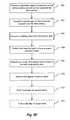
- FIG. 5Eis a simplified flowchart illustrating a process of fabricating a substrate support according to yet another embodiment of the present invention.
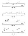
- FIGS. 6A-6Dare simplified schematic side view illustrations of a method of fabricating a substrate support according to an alternative embodiment of the present invention.
- FIG. 6Eis a simplified flowchart illustrating a method of fabricating a substrate support according to an alternative embodiment of the present invention.
- inventions and apparatus related to semiconductor manufacturing equipmentare provided. More particularly, embodiments of the present invention relate to a method and apparatus for supporting a substrate during semiconductor processing operations.
- the method and apparatuscan be applied to electrostatic chucks, vacuum chucks, and other applications as well.
- FIG. 1is a simplified schematic side view illustration of a substrate processing chamber according to one embodiment of the present invention.
- the assembly 180contains a plate assembly 170 and a vacuum source 175 , which are mounted in a processing module 186 .
- the plate assembly 170generally contains a plate 170 B, plate assembly surface 170 A, protrusions 171 , and a vacuum source port assembly 172 .
- the vacuum source 175is used to create a negative pressure in the vacuum port plenum 172 B, thus causing air to flow into a number of vacuum ports 172 A formed in the surface of the plate assembly 170 , thus creating a reduced pressure behind the substrate W which causes the substrate W to be biased towards to the surface of the proximity pins 171 .
- the plate 170 Bmay be made from a thermally conductive material such as aluminum, copper, graphite, aluminum-nitride, boron nitride, silicon carbide, and/or other material, and is in communication with a heat exchanging device 183 A. Additionally, the plate may be made from anodized materials, including anodized aluminum and sealed anodized aluminum.
- FIG. 1illustrates a vacuum chuck, this is not required by the present invention.
- Alternative embodiments of the present inventionprovide methods and apparatus for supporting a substrate using an electrostatic chuck.
- the plate assembly 170also contains a gas source port assembly 173 and a gas source 174 to purge the edge of the substrate during processing to prevent evaporating solvent vapors from being deposited on the plate assembly surface 170 A or the backside of the substrate due to the reduced pressure generated behind the substrate (e.g., a vacuum chuck configuration).
- the gas source 174is used to create a positive pressure in the gas port plenum 173 B, thus causing the gas to flow out of a plurality of gas ports 173 A formed in the surface of the plate assembly 170 .
- the gas source 174is adapted to deliver an inert gas to the edge of the substrate, such as, argon, xenon, helium, nitrogen, and/or krypton.
- the gas source 174may also be adapted to deliver a fluid to the edge of the substrate.
- additional gas ports and their associated gas lines and sourcesmay be provided as heat transfer aids.
- helium gasis provided through appropriate ports to the backside of the substrate to cool the substrate as part of a processing sequence.
- FIG. 2is a simplified schematic plan view of a vacuum chuck according to one embodiment of the present invention.
- the surface of the plate assembly 170is illustrated in FIG. 2 with no substrate on top of the proximity pins 171 .
- this figureillustrates one possible configuration of proximity pins 171 ( 33 shown), vacuum ports 172 A ( ⁇ 367 shown), and gas ports 173 A ( ⁇ 360 shown).
- a number of proximity pins 171are spaced across the surface of the plate assembly 170 so that the contact area can be minimized and the gap between the substrate and the plate assembly surface 170 A can be maintained at a substantially uniform distance.
- a number of vacuum ports 172 Aare spaced across the surface of the plate assembly 170 so that the substrate can be uniformly biased towards the plate assembly 170 , providing for a substantially uniform gap between the substrate and the plate assembly surface 170 A.
- an inner array of vacuum ports 172 A(see item “A”) is mirrored with an outer array of gas ports 173 A (see item “B”), where the diameter of the inner array “A” is smaller than the substrate diameter.
- vacuum portsare positioned under the substrate.
- the diameter of the outer array “B”is equal to or larger than the substrate diameter, but less than the diameter of the plate assembly.
- the diameter of the vacuum ports located across the surface of the plate assemblyvaries as a function of position.
- the vacuum ports arrayed as item “A”have a diameter smaller than vacuum ports distributed across the interior portions of the surface of the plate assembly.
- thisis not required by the present invention.
- the vacuum port diametersare equal or varied in other manners.
- a small ridge of materialis placed between the inner array of vacuum ports 172 and the outer array of gas ports 173 to minimize the amount of gas required to purge the edge of the substrate.
- material deposited by chemical vapor deposition (CVD) or physical vapor deposition (PVD)is used to form the proximity pins 171 and the small ridge of material placed between the inner array of vacuum ports 172 A and the outer array of gas ports 173 A.
- FIGS. 1 and 2also illustrate a configuration having a lift assembly 87 and lift pin hole 189 extending through the plate assembly surface 170 A to lift the substrate off the plate assembly surface 170 A.
- the gas delivered from the gas source 174is heated prior to exiting the gas ports 172 A to prevent cooling of the edge of the substrate W during processing.
- the length of the gas port plenum 173 B in the plate assembly 170is designed to assure that the gas resides in the gas port plenum long enough for the injected gas to substantially achieve the plate temperature before it exits the gas ports 172 A.
- other gasesmay be delivered from various ports (not shown) to either cool or heat the substrate as appropriate.
- the thermal couplingis increased by decreasing the distance between the substrate and the chuck. As evident to one of skill in the art, decreasing the spacing between the substrate and the chuck will lead to an increase in convective heat transfer across the gap.
- increasing the contact area between the substrate backside surface and the surface of the plate assembly 170will increase the thermal coupling and reduce the time it takes a substrate to reach the desired process temperature.
- increasing the contact areais often undesirable since it will generally increase the number of particles generated on the backside of the substrate, which can adversely impact the processing results and cause defects in the circuitry fabricated upon the substrate.
- One method of reducing the number of particles generated on the backside of the substrateis to minimize the contact area of the substrate to the surface of the plate assembly. Accordingly, an array of proximity pins or proximity pins that space the substrate off the surface of the plate assembly have been utilized. While the use of proximity pins reduces the number of particles generated, they may tend to reduce the thermal coupling between the substrate and the plate assembly. Therefore, it is often desirable to minimize the height of the proximity pins above the surface of the plate assembly to improve the thermal coupling, while also assuring that the substrate will not touch the surface of the plate assembly. Some applications have used sapphire spheres that are pressed or placed into machined holes in the plate assembly surface to act as proximity pins. However, it is often difficult to mechanically control the height to which the spheres extend above the surface of the plate assembly.
- one embodiment of the present inventionprovides an array of accurately controlled small contact area proximity pins 171 that are formed on the surface of the plate assembly 170 .
- the substrateis biased towards the plate assembly by vacuum ports to increase the thermal coupling between the substrate and the plate assembly.
- the substratemay be biased towards the plate assembly 170 by use of a vacuum chucking device.
- other embodiments of the present inventionutilize an electrostatic chucking device or other conventional methods of forcing the substrate against plate assembly.
- the array of accurately controlled small height proximity pins 171can be formed by a variety of methods, as described more fully below.
- a number of proximity pinsare distributed across the face of plate assembly 170 .
- 17 proximity pinsare utilized with the following locations: one pin at the center, four pins arranged at corners of a square concentric with the center pin, with a side equal to 50 mm, twelve pins arranged near the periphery of the plate assembly, separated from each other by arcs of 300.
- the proximity pinsare fabricated from a material with a low coefficient of friction. Accordingly, contact between the proximity pins and the substrate will produce a reduced number of particles.
- a two-step chucking processis utilized to flatten the wafer in a step-wise fashion.
- substrates or waferspossess a degree of bowing or warpage before they are place on the chuck.
- embodiments of the present inventionuse methods and systems to reduce wafer bowing, providing an increase in the uniformity of the gap between the wafer and the chuck surface.
- a first chucking stepis used in which a first chucking voltage is applied to initially remove a first amount of wafer bowing.
- a second chucking voltageis applied to maintain the wafer bowing profile achieved using the first chucking voltage.
- the second chucking voltageis less than the first chucking voltage.
- the pressure applied by an e-chuckincreases with chucking voltage.
- the amount of pressure required to flatten a substrateincreases with increased bowing.
- a high chucking voltageis used to apply a first high pressure, substantially flattening a substrate characterized by a first amount of wafer bowing.
- this chucking processmay be performed in more than two steps, incrementally decreasing the chucking voltage over a number of steps.
- FIGS. 3A-3Care simplified schematic side view illustrations of a method of fabricating a substrate support according to one embodiment of the present invention.
- a plate 300is provided.
- the plateis adapted to support a substrate, for example a silicon wafer, during semiconductor processing operations.
- various components of the plate assemblyincluding vacuum and purge ports, electrodes for electrostatic chucking mechanisms, heat exchanger elements, lift pin holes, etc. are omitted from the figures.
- the plateis one portion of a larger plate assembly as illustrated in FIG. 1 .
- the plate 300is an aluminum plate coated with a polymer.
- the platemay be an aluminum plate coated with Teflon® manufactured by Dupont Incorporated of Wilmington, Del. or Tufram® manufactured by General Magnaplate Corporation of Linden, N.J.
- plate 405is fabricated from stainless steel, silicon carbide, copper, graphite, aluminum, aluminum nitride, aluminum oxide, boron nitride, or combinations/laminates of these materials.
- recessed regions 302are formed in an upper surface 304 of the plate 300 .
- the recessed regions 302are formed by methods well known to one of skill in the art, for example, etching, ion milling, electric discharge machining, or laser ablation.
- a seed crystal 310is embedded in the plate 300 .
- the seed crystalis approximately the same size as the recessed region. Therefore, embedding of the seed crystal in the plate 300 constitutes a relatively permanent affixing of the seed crystal to the plate.
- the seed crystalmay be diamond, silicon, silicon oxide, boron nitride, aluminum oxide, and silicon carbide, or other material that is suitably hard.
- a seed crystal 310is embedded into each of the recessed regions 302 so that the top surface of the seed crystal is substantially flush with the plate surface 304 .
- a tool that has a surface that is at least as hard as the material from which the seed crystal 310 is madeis used to embed the seed crystal in the plate 300 .
- the tool materialis preferably relatively incompressible, has low ductility, and has a polished face.
- a suitable toolis a sapphire disk manufactured by Saint-Gobain Saphikon, Inc., of Miford, N.H.
- the surface of the sapphire diskis preferably characterized by flatness specifications such as a RMS roughness on the order of 5,000 ⁇ over a lateral distance of 10 mm and a radius of curvature of 12.5 m over a lateral distance of 10 mm.
- the toolis used in a method that embeds the seed crystal 310 in a repeatable manner so that the seed crystal is installed substantially flush with the plate surface 310 .
- proximity pins 320are selectively deposited on the seed crystal 310 using a CVD or PVD process.
- CVD and PVD processesenable the deposition of a thin layer of material of controlled size, producing a uniform layer of desired thickness on the surface of the plate assembly.
- the material deposited on the surface of the plate 300 to form the proximity pins 320may be diamond, diamond-like carbon, sapphire, boron nitride, silicon dioxide (SiO 2 ), silicon (Si), a metal (e.g., nickel, titanium, titanium nitride, molybdenum, tungsten), a ceramic material, a polymeric material (e.g., polyimide or Teflon®) or other suitable material.
- a suitable materialis hard enough to withstand the biasing force without appreciable deformation and is not easily abraded by the interaction with backside of the substrate.
- the proximity pins 320are formed on the seed crystals 310 .
- a homoepitaxial growth process performed using a methane/hydrogen/oxygen environment in a microwave plasma CVD chamberis used to form the proximity pins.
- growth rates of up to tens of microns per hourcan be achieved.
- the height 322 of the proximity pin 320can be controlled to a predetermined tolerance.
- the toleranceis ⁇ 10 ⁇ m.
- the toleranceis controlled within a range extending from about ⁇ 10 ⁇ m to about ⁇ 30 ⁇ m.
- FIGS. 4A-4Dare simplified schematic side view illustrations of a method of fabricating a substrate support according to another embodiment of the present invention.
- a plate 405is provided.
- the plateis adapted to support a substrate, for example a silicon wafer, during semiconductor processing operations.
- various components of the plate assemblyincluding vacuum and purge ports, electrodes for electrostatic chucking mechanisms, heat exchanger elements, lift pin holes, etc. are omitted from the figures.
- the plateis one portion of a larger plate assembly as illustrated in FIG. 1 .
- the plate 405is an aluminum plate coated with a polymer.
- plate 405is fabricated from stainless steel, silicon carbide, copper, graphite, aluminum, aluminum nitride, aluminum oxide, boron nitride, or combinations/laminates of these materials.
- a number of recessed regions 412are formed in surface 410 of the plate 405 . As illustrated in FIG. 4A , the recessed regions 412 are formed through a portion of the plate 405 using methods well known to one of skill in the art. In a specific embodiment, the recessed regions are fabricated with a predetermined width 416 and depth 414 . In the embodiment of the present invention illustrated in the figure, the recessed regions are generally cylindrical in shape, although this is not required by the present invention. Recessed regions of other shapes, for example, square, are utilized in alternative embodiments. In a specific embodiment, the width 416 of the recessed region is 1 mm and the depth 414 is 2 mm.
- the widthranges from about 0.2 mm to about 3 mm and the depth ranges from about 0.5 mm to about 5 mm. In a particular embodiment, the width and depth are equal, forming a cylinder with a diameter equal to the height.
- Support members 420are provided and placed in recessed regions 412 . As illustrated in FIG. 4B , the support members 420 are spherical in shape and have a diameter greater than the width of the recessed regions. Accordingly, a portion of the support members extends above the surface 410 of the plate 405 after initial placement.
- the support membersare sapphire precision spheres of predetermined diameter.
- sapphire precision spheres of a diameter of 0.5 mm with a sphericity of 0.000025′′ and a basic diameter tolerance of ⁇ 0.0001′′are available from Meller Optics, Inc. of Buffalo R.I.
- the tolerancecan be as low as 0.00005′′.
- the support membersare pressed into the plate or substrate support 405 so that an upper surface 424 of the support member lies in the plane defined by the upper surface 410 of the plate.
- a toolthat has a surface that is at least as hard as the material from which the support member is made, is used to embed the support member in the plate 405 .
- the tool materialis preferably relatively incompressible, flat, and has a polished face.
- a suitable toolis the Supercool 300 mm chuck manufactured by ERS-GmbH of Kunststoff, Germany.
- the surface 432 of plateis characterized by a RMS roughness of 20,000 ⁇ over a distance of 10 mm.
- sapphire precision spherescan be forced into the substrate support plate by applying downward pressure from a relatively incompressible, flat plate 432 placed adjacent to surface 410 of the plate.
- flat plate 430 with tool surface 432is placed adjacent the surface 410 and plates 405 and 430 are pressed together.
- the material from which the flat plate 430 is fabricatedis selected to possess a level of hardness greater than or equal to the hardness of the support member material, which in turn, is selected to possess a level of hardness greater than or equal to the hardness of the substrate support plate 405 .
- sapphirewith a hardness of about 40 GPa (compared to diamond with a hardness of about 90 GPa), is generally considered one of the hardest materials.
- applying pressure to the upper surface of a sapphire ball, as illustrated in FIG. 4Cwill deform the a substrate support plate fabricated from softer materials. Accordingly, the sapphire spheres will be forced into the recessed region, locally deforming the regions of the substrate support plate adjacent the recessed regions.
- the support membersAfter deformation of the substrate support plate, the support members will be embedded into the plate to a depth greater than the original depth of the recessed regions, represented by reference numeral 434 . Moreover, the width of the recessed region will be extended to a width greater than the original width at some portions of the structure.
- the substrate support plateis an aluminum plate, which generally has a hardness approximately ten times less that of sapphire, the substrate support plate will deform to receive the sapphire spheres as illustrated in the figure.
- Some embodiments of the present inventionutilize an embedding tool equal in diameter to the diameter of the plate 405 .
- an embedding tool with a diameter less than the diameter of the plate 405is utilized to force one or more support members into plate 405 simultaneously or sequentially. After the step of forcing the support members into the plate illustrated in FIG. 4C , the support members are flush with the surface 410 .
- FIG. 4Dillustrates a process of removing a portion of the substrate support plate to expose proximity pins extending above a third surface 438 of the plate by a height 442 .
- One embodiment of the present inventionutilizes an electropolishing process performed in a bath to remove a predetermined portion of the plate 405 and expose the third surface 438 .
- an electropolishing processan amount of material is removed proportional to the total charge, providing measurement and control over the amount of material removed.
- the electropolishing processis utilized to remove an amount of material characterized by a height equal to a predetermined fraction of the size of the support member. For example, as illustrated in FIG.
- the height 442 of the material removed from the plateis equal to about 20% of the diameter of the sapphire precision sphere.
- greater or lesser materialis removed as a percentage of the support member dimensions.
- the presence of the coatingis accounted for during the fabrication process.
- an additional amount of materialis removed during the electropolishing process equal to the thickness of the Teflon® layer eventually deposited, for example, 200 ⁇ .
- a selective coating processis performed to form the Teflon® layer.
- the selective coating processforms the coating layer only on the substrate support plate and not the proximity pins. Therefore, the final proximity pin height above the Teflon® layer, for example, is controlled by the combination of additional electropolishing counterbalanced by the formation of the Teflon® layer.
- an amount of material of depth 438is removed from the upper surface of the plate, with the electropolishing process being terminated once the upper plate surface reaches the plane defined by third surface 438 .
- proximity pins of a desired heightare produced utilizing embodiments of the present invention.
- the electropolishing processis utilized to remove 30 ⁇ m of material measured from surface 410 of plate 405 .
- proximity pins 420extend to a height of 30 ⁇ m above surface 438 .
- the height of the proximity pinsis greater or less than 30 ⁇ m. Therefore, embodiments of the present invention provide methods and apparatus for forming proximity pins of controllable height on a surface of a substrate support plate.
- FIGS. 5A-5Dare simplified schematic side view illustrations of a method of fabricating a substrate support according to yet another embodiment of the present invention.
- a plate 500is provided.
- the plateis adapted to support a substrate, for example a silicon wafer, during semiconductor processing operations.
- various components of the plate assemblyincluding vacuum and purge ports, electrodes for electrostatic chucking mechanisms, heat exchanger elements, lift pin holes, etc. are omitted from the figures.
- the plateis one portion of a larger plate assembly as illustrated in FIG. 1 .
- the plate 405is an aluminum plate coated with a polymer.
- plate 405is fabricated from stainless steel, silicon carbide, copper, graphite, aluminum, aluminum nitride, aluminum oxide, boron nitride, or combinations/laminates of these materials.
- Layer 510is deposited on the plate 500 .
- the material deposited on the surface of the plate 500 to form layer 510may be diamond, diamond-like carbon, sapphire, boron nitride, silicon dioxide (SiO 2 ), silicon (Si), aluminum oxynitride, a metal (e.g., nickel, titanium, titanium nitride, molybdenum, tungsten), a ceramic material, a polymeric material (e.g., polyimide or Teflon®) or other suitable material.
- a suitable materialis hard enough to withstand the biasing force without appreciable deformation, is not easily abraded by the interaction with backside of the substrate, and can be patterned after deposition. Control of deposition processes to achieve repeatable and uniform deposition of layers is well known to one of skill in the art.
- a mask layeris deposited and patterned as illustrated in FIG. 5B to form a number of masking structures 520 with a lateral dimension equal to distance 522 .
- Patterning of mask layersis well known to one of ordinary skill in the art.
- layer 510is selectively removed to form a number of proximity pins 530 .
- the making structures 520are not modified during the proximity pin formation process.
- the masking structuresdegrade during the proximity pin formation process, resulting in proximity pins with tapered upper surfaces. For example, masking structure that erode at the edges permit the proximity pin formation process to begin removing outer portions of the proximity pins prior to centrally located portions.
- some embodiments of the present inventionprovide a method of manufacturing proximity pins with tapered upper surfaces.
- One of ordinary skill in the artwould recognize many variations, modifications, and alternatives.
- proximity pins 530are removed as illustrated in FIG. 5D to expose proximity pins 530 .
- the proximity pinswill have predetermined heights and lateral dimensions. In the embodiment illustrated in FIG. 5D , proximity pins with a height of 30 ⁇ m and lateral dimensions of several millimeters are provided. In alternative embodiments, proximity pins with greater or lesser heights are provided.
- proximity pins utilizing masking structures deposited on a proximity pin layerwere described in reference to FIGS. 5A to 5 D, the present invention as illustrated in FIGS. 5A to 5 D is not limited to this fabrication method.
- An alternative formation methodutilizes other selective deposition processes to form the proximity pins.
- a stencil mask(not shown) is placed over the surface of the plate 500 , thereby allowing CVD or PVD material to be deposited (in lieu of layer 510 ) on certain defined areas of the substrate by use of features or holes formed in the stencil mask.
- the lateral dimensions of the proximity pinsare controlled by the features formed in the mask and the height of the proximity pins can be controlled by assuring a certain amount of material is deposited on the surface of the plate 500 using a known PVD or CVD process deposition rate.
- the proximity pins which are deposited by a PVD or CVD processare about 100 ⁇ m thick.
- a process utilizing a stencil mask to fabricate a substrate supportis illustrated as follows.
- a substrate support memberis provided, the substrate support member having a first surface and a second surface opposite the first surface.
- a stencil maskis provided having a solid background and a number of open features arrayed on the solid background. The stencil mask is positioned in relation to the substrate support member and the combination is exposed to a deposition process such that deposited materials pass through the open features to form a number of proximity pins in contact with the first surface. After deposition, the stencil mask is removed to expose the number of proximity pins.
- FIG. 5Eis a simplified flowchart illustrating a process of fabricating a substrate support according to yet another embodiment of the present invention.
- a substrate supportis provided, the substrate support has a first surface and a second surface opposite the first surface.
- the substrate supportis a thermally conductive material.
- a spacer layeris deposited over the first surface in step 562 .
- a PVD or CVD processis utilized to deposit the spacer layer.
- the thickness of the spacer layeris a predetermined thickness, for example, less than 100 ⁇ m.
- a masking layeris deposited over the spacer layer and the masking layer is patterned in step 566 to form a spacer structure mask.
- the spacer structure maskhas predetermined lateral dimensions. In a specific embodiment, the lateral surface area of the spacer structure mask is less than 3% of the surface area of the first surface.
- the spacer layeris selectively removed in unmasked areas of the spacer layer to form a number of proximity pins.
- Techniques for etching and removing materialsare well known to one of skill in the art.
- the spacer structure maskerodes during the spacer layer removal process, producing proximity pins with tapered upper surfaces. For example, in embodiments in which the spacer structure mask preferentially erodes at the edges, proximity pins with an upper surface characterized by a cross-section defined by an arc of a hemisphere are produced.
- the etching or removal processare continued to remove an upper strata of the first surface in unmasked areas of the spacer layer.
- the spacer structure maskis removed to expose the plurality of proximity pins.
- Optional steps 572 and 574form a plurality of vacuum ports passing from the first surface to the second surface and a plurality of purge ports passing from the second surface to the first surface, respectively.
- the plurality of purge portsare arranged in a first circular pattern, wherein the first circular pattern has a first radial dimension less than the radius of the substrate support plate.
- the plurality of vacuum portsare arranged in a second circular pattern, the second circular pattern having a second radial dimension less than the first radial dimension.
- the first circular pattern and the second circular patternare concentric.
- FIGS. 6A-6Dare simplified schematic side view illustrations of a method of fabricating a substrate support according to an alternative embodiment of the present invention.
- a plate 600is provided.
- the plateis adapted to support a substrate, for example a silicon wafer, during semiconductor processing operations.
- various components of the plate assemblyincluding vacuum and purge ports, electrodes for electrostatic chucking mechanisms, heat exchanger elements, lift pin holes, etc. are omitted from the figures.
- the plateis one portion of a larger plate assembly as illustrated in FIG. 1 .
- the plate 600is an aluminum plate coated with a polymer.
- plate 600is fabricated from stainless steel, silicon carbide, copper, graphite, aluminum, aluminum nitride, aluminum oxide, boron nitride, or combinations/laminates of these materials.
- a mask layeris deposited and patterned as illustrated in FIG. 6B to form a number of masking structures 610 with predetermined lateral dimensions. Patterning of mask layers is well known to one of ordinary skill in the art.
- individual masking structuresare bonded to surface 605 of plate 600 .
- ⁇ -Al 2 O 3 or diamond studsmay be epoxied to surface 605 to provide masking structures 610 .
- a processis performed to selectively remove a portion 620 of plate 600 .
- a grit-blasting techniqueis utilized to remove portion 620 of a silicon carbide plate, producing the structure illustrated in FIG. 6C .
- Masking structures 610are removed to expose proximity pins 640 with a predetermined height 642 and predetermined lateral dimensions.
- proximity pinsextend to a predetermined distance above surface 644 , for example, a height of 30 ⁇ m measured from surface 644 and lateral dimensions of several millimeters are provided. In alternative embodiments, proximity pins with greater or lesser heights are provided.
- making structures 610are not modified during the proximity pin formation process.
- the masking structuresdegrade during the proximity pin formation process, resulting in proximity pins with tapered upper surfaces.
- masking structures that erode at the edges during a grit-blasting processpermit the proximity pin formation process to begin removing outer portions of the proximity pins prior to centrally located portions.
- some embodiments of the present inventionprovide a method of manufacturing proximity pins with tapered upper surfaces.
- FIG. 6Eis a simplified flowchart illustrating a method of fabricating a substrate support according to an alternative embodiment of the present invention.
- a substrate support memberis provided, the member comprising a first surface and a second surface opposite the first surface.
- the substrate support memberis fabricated from silicon carbide.
- a number of spacer structure masksare bonded to the first surface in step 672 .
- Embodiments according to the present inventionutilize a number of different materials for spacer structure masks, including ⁇ -Al 2 O 3 , diamond, polymeric resins, silicone, polyimide, and vinyl.
- the spacer structure masksare polycrystalline.
- the spacer structure masksare bonded to the first surface utilizing an epoxy.
- a portion of the substrate support member defined by a depth measured from the first surface to a third surfaceis removed to form a plurality of proximity pins projecting to a first height above a third surface.
- the process of removing a portion of the first surfaceincludes grit blasting the first surface to form the proximity pins.
- the portion of the first surface removed by grit blastingis a layer less than 100 ⁇ m in thickness.
- the spacer structure masksare removed in step 676 .
- a number of vacuum ports passing from the third surface to the second surface and a number of purge ports passing from the second surface to the third surfaceare formed, respectively.
Landscapes
- Engineering & Computer Science (AREA)
- General Physics & Mathematics (AREA)
- Physics & Mathematics (AREA)
- Manufacturing & Machinery (AREA)
- Microelectronics & Electronic Packaging (AREA)
- Power Engineering (AREA)
- Computer Hardware Design (AREA)
- Condensed Matter Physics & Semiconductors (AREA)
- Robotics (AREA)
- General Engineering & Computer Science (AREA)
- Quality & Reliability (AREA)
- Automation & Control Theory (AREA)
- Container, Conveyance, Adherence, Positioning, Of Wafer (AREA)
- Coating Apparatus (AREA)
- Exposure Of Semiconductors, Excluding Electron Or Ion Beam Exposure (AREA)
- Exposure And Positioning Against Photoresist Photosensitive Materials (AREA)
- Manipulator (AREA)
- Photosensitive Polymer And Photoresist Processing (AREA)
- Materials For Photolithography (AREA)
Abstract
Description
- This application claims the benefit of U.S. Provisional Application Ser. No. 60/639,109, filed Dec. 22, 2004, entitled “Twin Architecture For Processing A Substrate,” which is incorporated herein by reference.
- The present invention relates generally to the field of semiconductor processing equipment. More particularly, the present invention relates to a method and apparatus for supporting a substrate inside a semiconductor processing chamber. The method and apparatus can be applied to electrostatic chucks, vacuum chucks, and other applications as well.
- Substrate support chucks are widely used to support substrates within semiconductor processing systems. Two examples of particular types of chucks used in semiconductor processing systems include electrostatic chucks (e-chucks) and vacuum chucks. These chucks are used to retain semiconductor wafers, or other workpieces, in a stationary position during processing.
- In some semiconductor processing systems, a substrate rests flush against the surface of the chuck body during processing. During substrate processing, the chuck material can abrade the material present on the underside of the substrate, resulting in the introduction of particulate contaminants to the process environment. Consequently, during substrate processing operations, the particles can adhere themselves to the underside of the substrate and be carried to other process chambers or cause defects in the circuitry fabricated upon the substrate.
- Therefore, a need exists in the art for methods and apparatus that reduce the amount of contaminant particles that adhere to the underside of a substrate during semiconductor processing.
- According to the present invention, methods and apparatus related to semiconductor manufacturing equipment are provided. More particularly, embodiments of the present invention relate to a method and apparatus for supporting a substrate during semiconductor processing operations. The method and apparatus can be applied to electrostatic chucks, vacuum chucks, and other applications as well.
- In a specific embodiment of the present invention, a substrate support structure is provided. The substrate support structure comprises a first surface and a second surface opposite the first surface. The substrate support structure also comprises a plurality of proximity pins projecting to a first height above the first surface, the first height being less than 100 μm. In addition, the substrate support structure further comprises a plurality of purge ports passing from the second surface to the first surface and a plurality of vacuum ports passing from the second surface to the first surface. In one particular embodiment, the plurality of purge ports are arranged in a first circular pattern, the first circular pattern having a first radial dimension less than the radius of the substrate support, and the plurality of vacuum ports are arranged in a second circular pattern, the second circular pattern having a second radial dimension less than the first radial dimension.
- In another specific embodiment of the present invention, a method of manufacturing a substrate support structure is provided. The method comprises providing a substrate support, the substrate support comprising a first surface and a second surface opposite the first surface, and forming a plurality of recessed regions in the first surface. The method also comprises providing a plurality of seed crystals having at least one planar surface and placing the plurality of seed crystals in the plurality of recessed regions so that the at least one planar face is coplanar with the first surface. The method further comprises selectively depositing a plurality of proximity pins in contact with the plurality of seed crystals and extending to a first height above the first surface.
- In yet another embodiment of the present invention, another method of manufacturing a substrate support structure is provided. The method comprises providing a substrate support, the substrate support comprising a first surface and a second surface opposite the first surface, and forming a plurality of recessed regions in the first surface, the plurality of recessed regions characterized by a first depth. The method also comprises providing a plurality of support structures characterized by a dimension greater than the first depth and inserting the plurality of support structures into the plurality of recessed regions. The method further comprises pressing the plurality of support structures into the plurality of recessed regions to align a surface of the plurality of support structures with the first surface, thereby deforming the plurality of recessed regions. Additionally, the method includes removing a portion of the substrate support defined by a depth measured from the first surface to a third surface to expose a portion of the support structures.
- Many benefits are achieved by way of the present invention over conventional techniques. For example, the present technique reduces the number of particles generated by contact between the backside surface of the substrate and the support plate. Moreover, embodiments of the present invention provide reduced height proximity pins while controlling the pin height to within a desired tolerance. The reduction in proximity pin height increases the thermal transfer rate of energy from the substrate to the plate assembly, thereby decreasing the time the substrate spends transitioning to a final temperature, increasing system throughput. Moreover, in some embodiments, an increase in thermal coupling between the substrate and plate assembly results in improvements in the thermally dependent properties of one or more films present on the surface of the substrate. Merely by way of example, for films in which control of a critical dimension is a function of diffusion and/or chemical reactions, improvements in control of the critical dimension may result from increased thermal coupling.
- Additionally, increased thermal coupling between the substrate and the plate assembly reduces the thermal impact of any chamber non-uniformities. Some embodiments of the present invention increase the thermal uniformity of the thermal transfer between the substrate and the plate assembly. Depending upon the embodiment, one or more of these benefits may be achieved. These and other benefits will be described in more detail throughout the present specification and more particularly below.
- These and other embodiments of the present invention, as well as its advantages and features, are described in more detail in conjunction with the text below and attached figures.
FIG. 1 is a simplified schematic side view illustration of a substrate processing chamber according to one embodiment of the present invention.FIG. 2 is a simplified schematic plan view of a vacuum chuck according to one embodiment of the present invention.FIGS. 3A-3C are simplified schematic side view illustrations of a method of fabricating a substrate support according to one embodiment of the present invention.FIGS. 4A-4D are simplified schematic side view illustrations of a method of fabricating a substrate support according to another embodiment of the present invention.FIGS. 5A-5D are simplified schematic side view illustrations of a method of fabricating a substrate support according to yet another embodiment of the present invention.FIG. 5E is a simplified flowchart illustrating a process of fabricating a substrate support according to yet another embodiment of the present invention.FIGS. 6A-6D are simplified schematic side view illustrations of a method of fabricating a substrate support according to an alternative embodiment of the present invention.FIG. 6E is a simplified flowchart illustrating a method of fabricating a substrate support according to an alternative embodiment of the present invention.- According to the present invention, methods and apparatus related to semiconductor manufacturing equipment are provided. More particularly, embodiments of the present invention relate to a method and apparatus for supporting a substrate during semiconductor processing operations. The method and apparatus can be applied to electrostatic chucks, vacuum chucks, and other applications as well.
FIG. 1 is a simplified schematic side view illustration of a substrate processing chamber according to one embodiment of the present invention. In the embodiment illustrated inFIG. 1 , theassembly 180 contains aplate assembly 170 and avacuum source 175, which are mounted in aprocessing module 186. Theplate assembly 170 generally contains aplate 170B,plate assembly surface 170A,protrusions 171, and a vacuumsource port assembly 172. In this configuration thevacuum source 175 is used to create a negative pressure in thevacuum port plenum 172B, thus causing air to flow into a number ofvacuum ports 172A formed in the surface of theplate assembly 170, thus creating a reduced pressure behind the substrate W which causes the substrate W to be biased towards to the surface of the proximity pins171. Theplate 170B may be made from a thermally conductive material such as aluminum, copper, graphite, aluminum-nitride, boron nitride, silicon carbide, and/or other material, and is in communication with aheat exchanging device 183A. Additionally, the plate may be made from anodized materials, including anodized aluminum and sealed anodized aluminum. AlthoughFIG. 1 illustrates a vacuum chuck, this is not required by the present invention. Alternative embodiments of the present invention provide methods and apparatus for supporting a substrate using an electrostatic chuck.- In one embodiment, the
plate assembly 170 also contains a gassource port assembly 173 and agas source 174 to purge the edge of the substrate during processing to prevent evaporating solvent vapors from being deposited on theplate assembly surface 170A or the backside of the substrate due to the reduced pressure generated behind the substrate (e.g., a vacuum chuck configuration). In this configuration thegas source 174 is used to create a positive pressure in thegas port plenum 173B, thus causing the gas to flow out of a plurality ofgas ports 173A formed in the surface of theplate assembly 170. In one embodiment thegas source 174 is adapted to deliver an inert gas to the edge of the substrate, such as, argon, xenon, helium, nitrogen, and/or krypton. Thegas source 174 may also be adapted to deliver a fluid to the edge of the substrate. In some embodiments, additional gas ports and their associated gas lines and sources, may be provided as heat transfer aids. For example, in one particular embodiment, helium gas is provided through appropriate ports to the backside of the substrate to cool the substrate as part of a processing sequence. One of ordinary skill in the art would recognize many variations, modifications, and alternatives. FIG. 2 is a simplified schematic plan view of a vacuum chuck according to one embodiment of the present invention. The surface of theplate assembly 170 is illustrated inFIG. 2 with no substrate on top of the proximity pins171. Thus, this figure illustrates one possible configuration of proximity pins171 (33 shown),vacuum ports 172A (˜367 shown), andgas ports 173A (˜360 shown). In general a number of proximity pins171 are spaced across the surface of theplate assembly 170 so that the contact area can be minimized and the gap between the substrate and theplate assembly surface 170A can be maintained at a substantially uniform distance.- In addition, a number of
vacuum ports 172A are spaced across the surface of theplate assembly 170 so that the substrate can be uniformly biased towards theplate assembly 170, providing for a substantially uniform gap between the substrate and theplate assembly surface 170A. In one embodiment, as shown inFIG. 2 an inner array ofvacuum ports 172A (see item “A”) is mirrored with an outer array ofgas ports 173A (see item “B”), where the diameter of the inner array “A” is smaller than the substrate diameter. Thus, vacuum ports are positioned under the substrate. Moreover, the diameter of the outer array “B” is equal to or larger than the substrate diameter, but less than the diameter of the plate assembly. In the embodiment illustrated inFIG. 2 , the diameter of the vacuum ports located across the surface of the plate assembly varies as a function of position. In one particular embodiment, the vacuum ports arrayed as item “A” have a diameter smaller than vacuum ports distributed across the interior portions of the surface of the plate assembly. However, this is not required by the present invention. In alternative embodiments, the vacuum port diameters are equal or varied in other manners. One of ordinary skill in the art would recognize many variations, modifications, and alternatives. - In one embodiment, a small ridge of material is placed between the inner array of
vacuum ports 172 and the outer array ofgas ports 173 to minimize the amount of gas required to purge the edge of the substrate. As described more fully below, in some embodiments, material deposited by chemical vapor deposition (CVD) or physical vapor deposition (PVD) is used to form the proximity pins171 and the small ridge of material placed between the inner array ofvacuum ports 172A and the outer array ofgas ports 173A. FIGS. 1 and 2 also illustrate a configuration having alift assembly 87 andlift pin hole 189 extending through theplate assembly surface 170A to lift the substrate off theplate assembly surface 170A.- In one embodiment, the gas delivered from the
gas source 174 is heated prior to exiting thegas ports 172A to prevent cooling of the edge of the substrate W during processing. In another embodiment, the length of thegas port plenum 173B in theplate assembly 170 is designed to assure that the gas resides in the gas port plenum long enough for the injected gas to substantially achieve the plate temperature before it exits thegas ports 172A. As discussed above with respect to helium backside cooling, other gases may be delivered from various ports (not shown) to either cool or heat the substrate as appropriate. - Various methods have been employed to increase the thermal coupling of the substrate to the chuck and consequently the heat exchanging device. Increased thermal coupling allows for reduction in the processing time, increased system throughput, and increased control over critical dimensions (CD). In a specific embodiment of the present invention, the thermal coupling is increased by decreasing the distance between the substrate and the chuck. As evident to one of skill in the art, decreasing the spacing between the substrate and the chuck will lead to an increase in convective heat transfer across the gap.
- Moreover, increasing the contact area between the substrate backside surface and the surface of the
plate assembly 170 will increase the thermal coupling and reduce the time it takes a substrate to reach the desired process temperature. However, increasing the contact area is often undesirable since it will generally increase the number of particles generated on the backside of the substrate, which can adversely impact the processing results and cause defects in the circuitry fabricated upon the substrate. - One method of reducing the number of particles generated on the backside of the substrate is to minimize the contact area of the substrate to the surface of the plate assembly. Accordingly, an array of proximity pins or proximity pins that space the substrate off the surface of the plate assembly have been utilized. While the use of proximity pins reduces the number of particles generated, they may tend to reduce the thermal coupling between the substrate and the plate assembly. Therefore, it is often desirable to minimize the height of the proximity pins above the surface of the plate assembly to improve the thermal coupling, while also assuring that the substrate will not touch the surface of the plate assembly. Some applications have used sapphire spheres that are pressed or placed into machined holes in the plate assembly surface to act as proximity pins. However, it is often difficult to mechanically control the height to which the spheres extend above the surface of the plate assembly.
- Referring to
FIG. 1 , one embodiment of the present invention provides an array of accurately controlled small contact area proximity pins171 that are formed on the surface of theplate assembly 170. In the embodiment illustrated inFIG. 1 , the substrate is biased towards the plate assembly by vacuum ports to increase the thermal coupling between the substrate and the plate assembly. As illustrated, the substrate may be biased towards theplate assembly 170 by use of a vacuum chucking device. Additionally, other embodiments of the present invention utilize an electrostatic chucking device or other conventional methods of forcing the substrate against plate assembly. One of ordinary skill in the art would recognize many variations, modifications, and alternatives. The array of accurately controlled small height proximity pins171 can be formed by a variety of methods, as described more fully below. - In embodiments of the present invention, a number of proximity pins are distributed across the face of
plate assembly 170. For example, in one particular embodiment,17 proximity pins are utilized with the following locations: one pin at the center, four pins arranged at corners of a square concentric with the center pin, with a side equal to 50 mm, twelve pins arranged near the periphery of the plate assembly, separated from each other by arcs of 300. Preferably, the proximity pins are fabricated from a material with a low coefficient of friction. Accordingly, contact between the proximity pins and the substrate will produce a reduced number of particles. - According to calculations we have performed, it is desirable to select the distribution pitch of proximity pins across the face plate surface to achieve goals related to maximum substrate bowing. Utilizing a 74 mm pitch between adjacent proximity pins, we have determined that it is possible to support a substrate with a maximum bowing at the substrate edge of about 5 μm. In designs with a 50 mm pitch between adjacent proximity pins, the maximum substrate bowing can be reduced to about 2.8 μm. Of course, the particular maximum bowing desired by the system operator will depend on the particular applications.
- In some embodiments of the present invention, a two-step chucking process is utilized to flatten the wafer in a step-wise fashion. Generally, substrates or wafers possess a degree of bowing or warpage before they are place on the chuck. Thus, embodiments of the present invention use methods and systems to reduce wafer bowing, providing an increase in the uniformity of the gap between the wafer and the chuck surface. For example, in an embodiment utilizing an e-chuck, a first chucking step is used in which a first chucking voltage is applied to initially remove a first amount of wafer bowing. After the first chucking voltage is applied, reducing the wafer bowing to a second value, a second chucking voltage is applied to maintain the wafer bowing profile achieved using the first chucking voltage. In a specific embodiment, the second chucking voltage is less than the first chucking voltage. As will be apparent to one of skill in the art, the pressure applied by an e-chuck increases with chucking voltage. Moreover, the amount of pressure required to flatten a substrate increases with increased bowing. Thus, in this specific embodiment, a high chucking voltage is used to apply a first high pressure, substantially flattening a substrate characterized by a first amount of wafer bowing. After the initial voltage removes a significant portion of the substrate bowing, a reduced voltage is sufficient to maintain the desired substrate flatness. Of course, one of skill in the art will appreciate that this chucking process may be performed in more than two steps, incrementally decreasing the chucking voltage over a number of steps.
FIGS. 3A-3C are simplified schematic side view illustrations of a method of fabricating a substrate support according to one embodiment of the present invention. As illustrated inFIG. 3 , aplate 300 is provided. Generally, the plate is adapted to support a substrate, for example a silicon wafer, during semiconductor processing operations. For purposes of clarity, various components of the plate assembly, including vacuum and purge ports, electrodes for electrostatic chucking mechanisms, heat exchanger elements, lift pin holes, etc. are omitted from the figures. One of ordinary skill in the art will appreciate that the plate is one portion of a larger plate assembly as illustrated inFIG. 1 . In some embodiments, theplate 300 is an aluminum plate coated with a polymer. Merely by way of example, the plate may be an aluminum plate coated with Teflon® manufactured by Dupont Incorporated of Wilmington, Del. or Tufram® manufactured by General Magnaplate Corporation of Linden, N.J. In alternative embodiments,plate 405 is fabricated from stainless steel, silicon carbide, copper, graphite, aluminum, aluminum nitride, aluminum oxide, boron nitride, or combinations/laminates of these materials.- As illustrated in
FIG. 3A , recessedregions 302 are formed in anupper surface 304 of theplate 300. The recessedregions 302 are formed by methods well known to one of skill in the art, for example, etching, ion milling, electric discharge machining, or laser ablation. After formation of the recessed regions, aseed crystal 310 is embedded in theplate 300. In one embodiment, the seed crystal is approximately the same size as the recessed region. Therefore, embedding of the seed crystal in theplate 300 constitutes a relatively permanent affixing of the seed crystal to the plate. Merely by way of example, the seed crystal may be diamond, silicon, silicon oxide, boron nitride, aluminum oxide, and silicon carbide, or other material that is suitably hard. In this embodiment, aseed crystal 310 is embedded into each of the recessedregions 302 so that the top surface of the seed crystal is substantially flush with theplate surface 304. - In one aspect of the invention, a tool that has a surface that is at least as hard as the material from which the
seed crystal 310 is made, is used to embed the seed crystal in theplate 300. In these embodiments, the tool material is preferably relatively incompressible, has low ductility, and has a polished face. One example of a suitable tool is a sapphire disk manufactured by Saint-Gobain Saphikon, Inc., of Miford, N.H. In an embodiment, the surface of the sapphire disk is preferably characterized by flatness specifications such as a RMS roughness on the order of 5,000 Å over a lateral distance of 10 mm and a radius of curvature of 12.5 m over a lateral distance of 10 mm. The tool is used in a method that embeds theseed crystal 310 in a repeatable manner so that the seed crystal is installed substantially flush with theplate surface 310. - As illustrated in
FIG. 3C , proximity pins320 are selectively deposited on theseed crystal 310 using a CVD or PVD process. For example, CVD and PVD processes enable the deposition of a thin layer of material of controlled size, producing a uniform layer of desired thickness on the surface of the plate assembly. The material deposited on the surface of theplate 300 to form the proximity pins320 may be diamond, diamond-like carbon, sapphire, boron nitride, silicon dioxide (SiO2), silicon (Si), a metal (e.g., nickel, titanium, titanium nitride, molybdenum, tungsten), a ceramic material, a polymeric material (e.g., polyimide or Teflon®) or other suitable material. Generally, a suitable material is hard enough to withstand the biasing force without appreciable deformation and is not easily abraded by the interaction with backside of the substrate. - Preferably, selective epitaxy or deposition processes are used to form the proximity pins320 on the
seed crystals 310. In one embodiment, a homoepitaxial growth process performed using a methane/hydrogen/oxygen environment in a microwave plasma CVD chamber is used to form the proximity pins. Depending on the growth parameters, including chamber temperature and chemistry, growth rates of up to tens of microns per hour can be achieved. Thus, using CVD or PVD processes, theheight 322 of theproximity pin 320 can be controlled to a predetermined tolerance. In one embodiment, the tolerance is ±10 μm. In alternative embodiments, the tolerance is controlled within a range extending from about ±10 μm to about ±30 μm. Thus, proximity pins with heights on the order of several to hundreds of microns are controllably provided by embodiments of the present invention. FIGS. 4A-4D are simplified schematic side view illustrations of a method of fabricating a substrate support according to another embodiment of the present invention. As illustrated inFIG. 4A , aplate 405 is provided. Generally, the plate is adapted to support a substrate, for example a silicon wafer, during semiconductor processing operations. For purposes of clarity, various components of the plate assembly, including vacuum and purge ports, electrodes for electrostatic chucking mechanisms, heat exchanger elements, lift pin holes, etc. are omitted from the figures. One of ordinary skill in the art will appreciate that the plate is one portion of a larger plate assembly as illustrated inFIG. 1 . In some embodiments, as discussed previously, theplate 405 is an aluminum plate coated with a polymer. In alternative embodiments,plate 405 is fabricated from stainless steel, silicon carbide, copper, graphite, aluminum, aluminum nitride, aluminum oxide, boron nitride, or combinations/laminates of these materials.- A number of recessed
regions 412 are formed insurface 410 of theplate 405. As illustrated inFIG. 4A , the recessedregions 412 are formed through a portion of theplate 405 using methods well known to one of skill in the art. In a specific embodiment, the recessed regions are fabricated with apredetermined width 416 anddepth 414. In the embodiment of the present invention illustrated in the figure, the recessed regions are generally cylindrical in shape, although this is not required by the present invention. Recessed regions of other shapes, for example, square, are utilized in alternative embodiments. In a specific embodiment, thewidth 416 of the recessed region is 1 mm and thedepth 414 is 2 mm. In alternative embodiments, the width ranges from about 0.2 mm to about 3 mm and the depth ranges from about 0.5 mm to about 5 mm. In a particular embodiment, the width and depth are equal, forming a cylinder with a diameter equal to the height. Support members 420 are provided and placed in recessedregions 412. As illustrated inFIG. 4B , thesupport members 420 are spherical in shape and have a diameter greater than the width of the recessed regions. Accordingly, a portion of the support members extends above thesurface 410 of theplate 405 after initial placement. In embodiments of the present invention, the support members are sapphire precision spheres of predetermined diameter. Merely by way of example, sapphire precision spheres of a diameter of 0.5 mm with a sphericity of 0.000025″ and a basic diameter tolerance of ±0.0001″ are available from Meller Optics, Inc. of Providence R.I. For sapphire precision spheres within the same lot, the tolerance can be as low as 0.00005″.- As illustrated in
FIG. 4C , the support members are pressed into the plate orsubstrate support 405 so that anupper surface 424 of the support member lies in the plane defined by theupper surface 410 of the plate. In one aspect of the invention, a tool that has a surface that is at least as hard as the material from which the support member is made, is used to embed the support member in theplate 405. In these embodiments, the tool material is preferably relatively incompressible, flat, and has a polished face. One example of a suitable tool is theSupercool 300 mm chuck manufactured by ERS-GmbH of Munich, Germany. Thesurface 432 of plate is characterized by a RMS roughness of 20,000 Å over a distance of 10 mm. Merely by way of example, as illustrated inFIG. 4C , sapphire precision spheres can be forced into the substrate support plate by applying downward pressure from a relatively incompressible,flat plate 432 placed adjacent to surface410 of the plate. - As illustrated in
FIG. 4C ,flat plate 430 withtool surface 432 is placed adjacent thesurface 410 andplates flat plate 430 is fabricated is selected to possess a level of hardness greater than or equal to the hardness of the support member material, which in turn, is selected to possess a level of hardness greater than or equal to the hardness of thesubstrate support plate 405. For example, sapphire, with a hardness of about 40 GPa (compared to diamond with a hardness of about 90 GPa), is generally considered one of the hardest materials. Thus, in applications which utilize flat plates and support members fabricated from sapphire, applying pressure to the upper surface of a sapphire ball, as illustrated inFIG. 4C , will deform the a substrate support plate fabricated from softer materials. Accordingly, the sapphire spheres will be forced into the recessed region, locally deforming the regions of the substrate support plate adjacent the recessed regions. - After deformation of the substrate support plate, the support members will be embedded into the plate to a depth greater than the original depth of the recessed regions, represented by
reference numeral 434. Moreover, the width of the recessed region will be extended to a width greater than the original width at some portions of the structure. - Merely by way of example, if the substrate support plate is an aluminum plate, which generally has a hardness approximately ten times less that of sapphire, the substrate support plate will deform to receive the sapphire spheres as illustrated in the figure. Some embodiments of the present invention utilize an embedding tool equal in diameter to the diameter of the
plate 405. In alternative embodiments, an embedding tool with a diameter less than the diameter of theplate 405 is utilized to force one or more support members intoplate 405 simultaneously or sequentially. After the step of forcing the support members into the plate illustrated inFIG. 4C , the support members are flush with thesurface 410. FIG. 4D illustrates a process of removing a portion of the substrate support plate to expose proximity pins extending above athird surface 438 of the plate by aheight 442. One embodiment of the present invention utilizes an electropolishing process performed in a bath to remove a predetermined portion of theplate 405 and expose thethird surface 438. In an electropolishing process, an amount of material is removed proportional to the total charge, providing measurement and control over the amount of material removed. In some embodiments, the electropolishing process is utilized to remove an amount of material characterized by a height equal to a predetermined fraction of the size of the support member. For example, as illustrated inFIG. 4D , theheight 442 of the material removed from the plate is equal to about 20% of the diameter of the sapphire precision sphere. Of course, in alternative embodiments, greater or lesser material is removed as a percentage of the support member dimensions. One of ordinary skill in the art would recognize many variations, modifications, and alternatives.- In embodiments of the present invention in which the substrate support plates are coated, the presence of the coating is accounted for during the fabrication process. For example, in a substrate support plate coated with Teflon®, an additional amount of material is removed during the electropolishing process equal to the thickness of the Teflon® layer eventually deposited, for example, 200 Å. Thus, after the substrate support plate is electropolished, exposing the proximity pins by an additional height of 200 Å, a selective coating process is performed to form the Teflon® layer. In one embodiment, the selective coating process forms the coating layer only on the substrate support plate and not the proximity pins. Therefore, the final proximity pin height above the Teflon® layer, for example, is controlled by the combination of additional electropolishing counterbalanced by the formation of the Teflon® layer.
- As illustrated in
FIG. 4D , an amount of material of depth438 (measured from the first surface to the third surface) is removed from the upper surface of the plate, with the electropolishing process being terminated once the upper plate surface reaches the plane defined bythird surface 438. Thus, proximity pins of a desired height are produced utilizing embodiments of the present invention. In a specific embodiment, the electropolishing process is utilized to remove 30 μm of material measured fromsurface 410 ofplate 405. Thus, proximity pins420 extend to a height of 30 μm abovesurface 438. In alternative embodiments, the height of the proximity pins is greater or less than 30 μm. Therefore, embodiments of the present invention provide methods and apparatus for forming proximity pins of controllable height on a surface of a substrate support plate. FIGS. 5A-5D are simplified schematic side view illustrations of a method of fabricating a substrate support according to yet another embodiment of the present invention. As illustrated inFIG. 5A , aplate 500 is provided. Generally, the plate is adapted to support a substrate, for example a silicon wafer, during semiconductor processing operations. For purposes of clarity, various components of the plate assembly, including vacuum and purge ports, electrodes for electrostatic chucking mechanisms, heat exchanger elements, lift pin holes, etc. are omitted from the figures. One of ordinary skill in the art will appreciate that the plate is one portion of a larger plate assembly as illustrated inFIG. 1 . In some embodiments, as discussed previously, theplate 405 is an aluminum plate coated with a polymer. In alternative embodiments,plate 405 is fabricated from stainless steel, silicon carbide, copper, graphite, aluminum, aluminum nitride, aluminum oxide, boron nitride, or combinations/laminates of these materials.Layer 510, with athickness 512, is deposited on theplate 500. The material deposited on the surface of theplate 500 to formlayer 510 may be diamond, diamond-like carbon, sapphire, boron nitride, silicon dioxide (SiO2), silicon (Si), aluminum oxynitride, a metal (e.g., nickel, titanium, titanium nitride, molybdenum, tungsten), a ceramic material, a polymeric material (e.g., polyimide or Teflon®) or other suitable material. Generally, a suitable material is hard enough to withstand the biasing force without appreciable deformation, is not easily abraded by the interaction with backside of the substrate, and can be patterned after deposition. Control of deposition processes to achieve repeatable and uniform deposition of layers is well known to one of skill in the art.- A mask layer is deposited and patterned as illustrated in
FIG. 5B to form a number of maskingstructures 520 with a lateral dimension equal todistance 522. Patterning of mask layers is well known to one of ordinary skill in the art. After patterning of the mask layer to form maskingstructures 520,layer 510 is selectively removed to form a number of proximity pins530. As illustrated inFIG. 5C , the makingstructures 520 are not modified during the proximity pin formation process. In alternative embodiments, the masking structures degrade during the proximity pin formation process, resulting in proximity pins with tapered upper surfaces. For example, masking structure that erode at the edges permit the proximity pin formation process to begin removing outer portions of the proximity pins prior to centrally located portions. Thus, some embodiments of the present invention provide a method of manufacturing proximity pins with tapered upper surfaces. One of ordinary skill in the art would recognize many variations, modifications, and alternatives. - The masking structures are removed as illustrated in
FIG. 5D to expose proximity pins530. Based on the deposition and masking processes described above, the proximity pins will have predetermined heights and lateral dimensions. In the embodiment illustrated inFIG. 5D , proximity pins with a height of 30 μm and lateral dimensions of several millimeters are provided. In alternative embodiments, proximity pins with greater or lesser heights are provided. - Although the formation of proximity pins utilizing masking structures deposited on a proximity pin layer were described in reference to
FIGS. 5A to5D, the present invention as illustrated inFIGS. 5A to5D is not limited to this fabrication method. An alternative formation method utilizes other selective deposition processes to form the proximity pins. For example, in one embodiment, a stencil mask (not shown) is placed over the surface of theplate 500, thereby allowing CVD or PVD material to be deposited (in lieu of layer510) on certain defined areas of the substrate by use of features or holes formed in the stencil mask. In this way the lateral dimensions of the proximity pins are controlled by the features formed in the mask and the height of the proximity pins can be controlled by assuring a certain amount of material is deposited on the surface of theplate 500 using a known PVD or CVD process deposition rate. In one embodiment, the proximity pins which are deposited by a PVD or CVD process are about 100 μm thick. - Merely by way of example, a process utilizing a stencil mask to fabricate a substrate support is illustrated as follows. A substrate support member is provided, the substrate support member having a first surface and a second surface opposite the first surface. A stencil mask is provided having a solid background and a number of open features arrayed on the solid background. The stencil mask is positioned in relation to the substrate support member and the combination is exposed to a deposition process such that deposited materials pass through the open features to form a number of proximity pins in contact with the first surface. After deposition, the stencil mask is removed to expose the number of proximity pins.
FIG. 5E is a simplified flowchart illustrating a process of fabricating a substrate support according to yet another embodiment of the present invention. Instep 560, a substrate support is provided, the substrate support has a first surface and a second surface opposite the first surface. In some embodiments, the substrate support is a thermally conductive material. A spacer layer is deposited over the first surface instep 562. In embodiments of the present invention, a PVD or CVD process is utilized to deposit the spacer layer. Moreover, the thickness of the spacer layer is a predetermined thickness, for example, less than 100 μm. Instep 564, a masking layer is deposited over the spacer layer and the masking layer is patterned instep 566 to form a spacer structure mask. The spacer structure mask has predetermined lateral dimensions. In a specific embodiment, the lateral surface area of the spacer structure mask is less than 3% of the surface area of the first surface.- In
step 568, the spacer layer is selectively removed in unmasked areas of the spacer layer to form a number of proximity pins. Techniques for etching and removing materials are well known to one of skill in the art. In some embodiments, the spacer structure mask erodes during the spacer layer removal process, producing proximity pins with tapered upper surfaces. For example, in embodiments in which the spacer structure mask preferentially erodes at the edges, proximity pins with an upper surface characterized by a cross-section defined by an arc of a hemisphere are produced. - Moreover, in other embodiments of the present invention, the etching or removal process are continued to remove an upper strata of the first surface in unmasked areas of the spacer layer. In
step 570, the spacer structure mask is removed to expose the plurality of proximity pins.Optional steps optional step 574, the plurality of purge ports are arranged in a first circular pattern, wherein the first circular pattern has a first radial dimension less than the radius of the substrate support plate. Additionally, in some embodiments employingoptional step 572, the plurality of vacuum ports are arranged in a second circular pattern, the second circular pattern having a second radial dimension less than the first radial dimension. Moreover, in some embodiments employing both optional steps, the first circular pattern and the second circular pattern are concentric. FIGS. 6A-6D are simplified schematic side view illustrations of a method of fabricating a substrate support according to an alternative embodiment of the present invention. As illustrated inFIG. 6A , aplate 600 is provided. Generally, the plate is adapted to support a substrate, for example a silicon wafer, during semiconductor processing operations. For purposes of clarity, various components of the plate assembly, including vacuum and purge ports, electrodes for electrostatic chucking mechanisms, heat exchanger elements, lift pin holes, etc. are omitted from the figures. One of ordinary skill in the art will appreciate that the plate is one portion of a larger plate assembly as illustrated inFIG. 1 . In some embodiments, as discussed previously, theplate 600 is an aluminum plate coated with a polymer. In alternative embodiments,plate 600 is fabricated from stainless steel, silicon carbide, copper, graphite, aluminum, aluminum nitride, aluminum oxide, boron nitride, or combinations/laminates of these materials.- In one, embodiment, a mask layer is deposited and patterned as illustrated in
FIG. 6B to form a number of maskingstructures 610 with predetermined lateral dimensions. Patterning of mask layers is well known to one of ordinary skill in the art. In alternative embodiments, individual masking structures are bonded to surface605 ofplate 600. For example, β-Al2O3or diamond studs may be epoxied to surface605 to provide maskingstructures 610. - After the masking structures are provided, a process is performed to selectively remove a
portion 620 ofplate 600. In a particular embodiment of the present invention, a grit-blasting technique is utilized to removeportion 620 of a silicon carbide plate, producing the structure illustrated inFIG. 6C . Maskingstructures 610 are removed to exposeproximity pins 640 with apredetermined height 642 and predetermined lateral dimensions. In the embodiment illustrated inFIG. 6D , proximity pins extend to a predetermined distance abovesurface 644, for example, a height of 30 μm measured fromsurface 644 and lateral dimensions of several millimeters are provided. In alternative embodiments, proximity pins with greater or lesser heights are provided. - As illustrated in
FIGS. 6B and 6C , makingstructures 610 are not modified during the proximity pin formation process. In alternative embodiments, the masking structures degrade during the proximity pin formation process, resulting in proximity pins with tapered upper surfaces. For example, masking structures that erode at the edges during a grit-blasting process permit the proximity pin formation process to begin removing outer portions of the proximity pins prior to centrally located portions. Thus, some embodiments of the present invention provide a method of manufacturing proximity pins with tapered upper surfaces. One of ordinary skill in the art would recognize many variations, modifications, and alternatives. FIG. 6E is a simplified flowchart illustrating a method of fabricating a substrate support according to an alternative embodiment of the present invention. Instep 670, a substrate support member is provided, the member comprising a first surface and a second surface opposite the first surface. In a specific embodiment, the substrate support member is fabricated from silicon carbide. A number of spacer structure masks are bonded to the first surface instep 672. Embodiments according to the present invention utilize a number of different materials for spacer structure masks, including β-Al2O3, diamond, polymeric resins, silicone, polyimide, and vinyl. In some embodiments, the spacer structure masks are polycrystalline. Moreover, in some embodiments of the present invention, the spacer structure masks are bonded to the first surface utilizing an epoxy.- In
step 674, a portion of the substrate support member defined by a depth measured from the first surface to a third surface is removed to form a plurality of proximity pins projecting to a first height above a third surface. According to embodiments of the present invention, the process of removing a portion of the first surface includes grit blasting the first surface to form the proximity pins. Moreover, in a particular embodiment, the portion of the first surface removed by grit blasting is a layer less than 100 μm in thickness. The spacer structure masks are removed instep 676. Inoptional steps - Accordingly, while the present invention has been disclosed in connection with the preferred embodiments thereof, it should be understood that other embodiments may fall within the spirit and scope of the invention, as defined by the following claims.
Claims (19)
1. A substrate support structure, the structure comprising:
a substrate support comprising a first surface and a second surface opposite the first surface;
a plurality of proximity pins projecting to a first height above the first surface, the first height being less than 100 μm;
a plurality of purge ports passing from the second surface to the first surface; and
a plurality of vacuum ports passing from the second surface to the first surface.
2. The substrate support structure ofclaim 1 wherein the plurality of purge ports are arranged in a first circular pattern, the first circular pattern having a first radial dimension less than the radius of the substrate support; and
the plurality of vacuum ports are arranged in a second circular pattern, the second circular pattern having a second radial dimension less than the first radial dimension.
3. The substrate support structure ofclaim 2 further comprising an annular spacer ridge characterized by a radial dimension greater than the second radial dimension and extending a second height above the first surface, wherein the second height is less than the first height.
4. The substrate support structure ofclaim 1 wherein the plurality of proximity pins comprise materials selected from the group consisting of silicon, silicon oxides, metals, ceramics, polymers, diamond, diamond-like carbon, boron nitride, single crystalline α-alumina, and polycrystalline β-alumina.
5. The substrate support structure ofclaim 1 wherein the substrate support is fabricated from a material selected from the group consisting of stainless steel, silicon carbide, copper, graphite, aluminum, aluminum nitride, aluminum oxide, boron nitride, anodized aluminum, and sealed anodized aluminum.
6. A method of manufacturing a substrate support structure, the method comprising:
providing a substrate support, the substrate support comprising a first surface and a second surface opposite the first surface;
forming a plurality of recessed regions in the first surface;
providing a plurality of seed crystals having at least one planar surface;
placing the plurality of seed crystals in the plurality of recessed regions so that the at least one planar face is substantially coplanar with the first surface; and
selectively depositing a plurality of proximity pins in contact with the plurality of seed crystals and extending to a first height above the first surface.
7. The method ofclaim 6 further comprising:
forming a plurality of vacuum ports passing from the first surface to the second surface; and
forming a plurality of purge ports passing from the second surface to the first surface.
8. The method ofclaim 6 wherein selectively depositing comprises a homoepitaxial growth process.
9. The method ofclaim 6 wherein the plurality of seed crystals are fabricated from a material selected from the group consisting of diamond, silicon, silicon oxide, boron nitride, and aluminum oxide.
10. The method ofclaim 6 wherein the first height is less than 100 μm.
11. A method of manufacturing a substrate support structure, the method comprising:
providing a substrate support, the substrate support comprising a first surface and a second surface opposite the first surface;
forming a plurality of recessed regions in the first surface, the plurality of recessed regions characterized by a first depth;
providing a plurality of support structures characterized by a dimension greater than the first depth;
inserting the plurality of support structures into the plurality of recessed regions;
pressing the plurality of support structures into the plurality of recessed regions to align a surface of the plurality of support structures with the first surface, thereby deforming the plurality of recessed regions;
removing a portion of the substrate support defined by a depth measured from the first surface to a third surface to expose to expose a portion of the support structures.
12. The method ofclaim 11 wherein the support structures are sapphire spheres.
13. The method ofclaim 12 wherein the dimension is a diameter of the sapphire spheres.
14. The method ofclaim 13 wherein the diameter is less than approximately 4 mm.
15. The method ofclaim 11 wherein the step of inserting the plurality of support structures into the plurality of recessed regions comprises at least a portion of the plurality of support structures extending to a second height above the first surface.
16. The method ofclaim 11 wherein the depth is approximately 30 μm.
17. The method ofclaim 11 wherein the step of removing a portion of the substrate support comprises electropolishing portions of the first surface of the substrate support.
18. The method ofclaim 17 wherein electropolishing portions of the first surface removes a layer of the substrate support less than 100 μm in thickness.
19. The method ofclaim 11 wherein pressing the plurality of support structures into the plurality of recessed regions and aligning a surface of the plurality of support structures with the first surface comprises using a tool with a level of hardness greater than or equal to a level of hardness of the support structures, the level of hardness of the support structures being greater than or a level of hardness of the substrate support.
Priority Applications (2)
| Application Number | Priority Date | Filing Date | Title |
|---|---|---|---|
| US11/111,155US20060130767A1 (en) | 2004-12-22 | 2005-04-20 | Purged vacuum chuck with proximity pins |
| US11/336,471US20060236941A1 (en) | 2005-04-20 | 2006-01-20 | Passive wafer support for particle free wafer acceleration |
Applications Claiming Priority (2)
| Application Number | Priority Date | Filing Date | Title |
|---|---|---|---|
| US63910904P | 2004-12-22 | 2004-12-22 | |
| US11/111,155US20060130767A1 (en) | 2004-12-22 | 2005-04-20 | Purged vacuum chuck with proximity pins |
Related Child Applications (1)
| Application Number | Title | Priority Date | Filing Date |
|---|---|---|---|
| US11/336,471Continuation-In-PartUS20060236941A1 (en) | 2005-04-20 | 2006-01-20 | Passive wafer support for particle free wafer acceleration |
Publications (1)
| Publication Number | Publication Date |
|---|---|
| US20060130767A1true US20060130767A1 (en) | 2006-06-22 |
Family
ID=39193608
Family Applications (18)
| Application Number | Title | Priority Date | Filing Date |
|---|---|---|---|
| US11/111,154Expired - LifetimeUS7255747B2 (en) | 2004-12-22 | 2005-04-20 | Coat/develop module with independent stations |
| US11/111,156Expired - LifetimeUS7371022B2 (en) | 2004-12-22 | 2005-04-20 | Developer endpoint detection in a track lithography system |
| US11/111,155AbandonedUS20060130767A1 (en) | 2004-12-22 | 2005-04-20 | Purged vacuum chuck with proximity pins |
| US11/111,353Active2026-03-10US7396412B2 (en) | 2004-12-22 | 2005-04-20 | Coat/develop module with shared dispense |
| US11/112,932AbandonedUS20060134330A1 (en) | 2004-12-22 | 2005-04-22 | Cluster tool architecture for processing a substrate |
| US11/112,281Expired - LifetimeUS7357842B2 (en) | 2004-12-22 | 2005-04-22 | Cluster tool architecture for processing a substrate |
| US11/147,037AbandonedUS20060134536A1 (en) | 2004-12-22 | 2005-06-06 | Method and system for determining post exposure bake endpoint |
| US11/316,329AbandonedUS20060158240A1 (en) | 2004-12-22 | 2005-12-21 | Distributed temperature control system for point of dispense temperature control on track systems utilizing mixing of hot and cold streams |
| US11/458,667Expired - Fee RelatedUS7925377B2 (en) | 2004-12-22 | 2006-07-19 | Cluster tool architecture for processing a substrate |
| US11/458,664Expired - LifetimeUS7694647B2 (en) | 2004-12-22 | 2006-07-19 | Cluster tool architecture for processing a substrate |
| US12/033,837AbandonedUS20080223293A1 (en) | 2004-12-22 | 2008-02-19 | Cluster tool architecture for processing a substrate |
| US12/106,824Expired - LifetimeUS7743728B2 (en) | 2004-12-22 | 2008-04-21 | Cluster tool architecture for processing a substrate |
| US12/136,006AbandonedUS20080296316A1 (en) | 2004-12-22 | 2008-06-09 | Coat/develop module with shared dispense |
| US12/254,778Expired - Fee RelatedUS8146530B2 (en) | 2004-12-22 | 2008-10-20 | Cluster tool architecture for processing a substrate |
| US12/254,784Expired - Fee RelatedUS8215262B2 (en) | 2004-12-22 | 2008-10-20 | Cluster tool architecture for processing a substrate |
| US12/254,750Expired - Fee RelatedUS8181596B2 (en) | 2004-12-22 | 2008-10-20 | Cluster tool architecture for processing a substrate |
| US13/411,120AbandonedUS20120180983A1 (en) | 2004-12-22 | 2012-03-02 | Cluster tool architecture for processing a substrate |
| US13/524,854Expired - LifetimeUS8550031B2 (en) | 2004-12-22 | 2012-06-15 | Cluster tool architecture for processing a substrate |
Family Applications Before (2)
| Application Number | Title | Priority Date | Filing Date |
|---|---|---|---|
| US11/111,154Expired - LifetimeUS7255747B2 (en) | 2004-12-22 | 2005-04-20 | Coat/develop module with independent stations |
| US11/111,156Expired - LifetimeUS7371022B2 (en) | 2004-12-22 | 2005-04-20 | Developer endpoint detection in a track lithography system |
Family Applications After (15)
| Application Number | Title | Priority Date | Filing Date |
|---|---|---|---|
| US11/111,353Active2026-03-10US7396412B2 (en) | 2004-12-22 | 2005-04-20 | Coat/develop module with shared dispense |
| US11/112,932AbandonedUS20060134330A1 (en) | 2004-12-22 | 2005-04-22 | Cluster tool architecture for processing a substrate |
| US11/112,281Expired - LifetimeUS7357842B2 (en) | 2004-12-22 | 2005-04-22 | Cluster tool architecture for processing a substrate |
| US11/147,037AbandonedUS20060134536A1 (en) | 2004-12-22 | 2005-06-06 | Method and system for determining post exposure bake endpoint |
| US11/316,329AbandonedUS20060158240A1 (en) | 2004-12-22 | 2005-12-21 | Distributed temperature control system for point of dispense temperature control on track systems utilizing mixing of hot and cold streams |
| US11/458,667Expired - Fee RelatedUS7925377B2 (en) | 2004-12-22 | 2006-07-19 | Cluster tool architecture for processing a substrate |
| US11/458,664Expired - LifetimeUS7694647B2 (en) | 2004-12-22 | 2006-07-19 | Cluster tool architecture for processing a substrate |
| US12/033,837AbandonedUS20080223293A1 (en) | 2004-12-22 | 2008-02-19 | Cluster tool architecture for processing a substrate |
| US12/106,824Expired - LifetimeUS7743728B2 (en) | 2004-12-22 | 2008-04-21 | Cluster tool architecture for processing a substrate |
| US12/136,006AbandonedUS20080296316A1 (en) | 2004-12-22 | 2008-06-09 | Coat/develop module with shared dispense |
| US12/254,778Expired - Fee RelatedUS8146530B2 (en) | 2004-12-22 | 2008-10-20 | Cluster tool architecture for processing a substrate |
| US12/254,784Expired - Fee RelatedUS8215262B2 (en) | 2004-12-22 | 2008-10-20 | Cluster tool architecture for processing a substrate |
| US12/254,750Expired - Fee RelatedUS8181596B2 (en) | 2004-12-22 | 2008-10-20 | Cluster tool architecture for processing a substrate |
| US13/411,120AbandonedUS20120180983A1 (en) | 2004-12-22 | 2012-03-02 | Cluster tool architecture for processing a substrate |
| US13/524,854Expired - LifetimeUS8550031B2 (en) | 2004-12-22 | 2012-06-15 | Cluster tool architecture for processing a substrate |
Country Status (3)
| Country | Link |
|---|---|
| US (18) | US7255747B2 (en) |
| JP (3) | JP2012069957A (en) |
| CN (2) | CN101443131B (en) |
Cited By (444)
| Publication number | Priority date | Publication date | Assignee | Title |
|---|---|---|---|---|
| US20070157466A1 (en)* | 2005-12-27 | 2007-07-12 | Nhk Spring Co., Ltd. | Substrate supporting apparatus and manufacturing method therefor |
| US20070247165A1 (en)* | 2006-04-25 | 2007-10-25 | Applied Materials, Inc. | Wafer backside particle detection for track tools |
| US20070247137A1 (en)* | 2006-04-25 | 2007-10-25 | Applied Materials, Inc. | Wafer bevel particle detection |
| US20070254493A1 (en)* | 2006-04-28 | 2007-11-01 | Applied Materials, Inc. | Integrated thermal unit having vertically arranged bake and chill plates |
| US20070295276A1 (en)* | 2004-12-22 | 2007-12-27 | Sokudo Co., Ltd. | Bake plate having engageable thermal mass |
| US20080145191A1 (en)* | 2006-11-15 | 2008-06-19 | Sokudo Co., Ltd. | Actively chilled substrate transport module |
| US20080164578A1 (en)* | 2006-12-28 | 2008-07-10 | Saint-Gobain Ceramics & Plastics, Inc. | Sapphire substrates and methods of making same |
| US20080164458A1 (en)* | 2006-12-28 | 2008-07-10 | Saint-Gobain Ceramics & Plastics, Inc. | Sapphire substrates and methods of making same |
| US20080166951A1 (en)* | 2006-12-28 | 2008-07-10 | Saint-Gobain Ceramics & Plastics, Inc. | Sapphire substrates and methods of making same |
| US20080171944A1 (en)* | 2005-07-26 | 2008-07-17 | Rox Medical, Inc. | Devices, systems, and methods for peripheral arteriovenous fistula creation |
| US20080179010A1 (en)* | 2007-01-26 | 2008-07-31 | Lam Research Corporation | Bevel etcher with vacuum chuck |
| US20090055124A1 (en)* | 2007-08-23 | 2009-02-26 | Sokudo Co., Ltd. | Method and System for Determining Object Height |
| US20090179365A1 (en)* | 2008-01-15 | 2009-07-16 | Lerner Alexander N | High temperature vacuum chuck assembly |
| US20100133735A1 (en)* | 2008-11-28 | 2010-06-03 | Canon Kabushiki Kaisha | Substrate holding apparatus, substrate holding method, exposure apparatus, and device manufacturing method |
| CN102129966A (en)* | 2009-12-15 | 2011-07-20 | 英特赛尔美国股份有限公司 | Method of forming a thermally conductive region in a semiconductor structure and structure obtained therefrom |
| US20120055916A1 (en)* | 2010-03-01 | 2012-03-08 | Sokudo Co., Ltd. | Method and system for thermal treatment of substrates |
| US20120313308A1 (en)* | 2011-06-08 | 2012-12-13 | Shenzhen China Star Optoelectronics Technology Co., Ltd. | Component Supporting Device |
| US20130014896A1 (en)* | 2011-07-15 | 2013-01-17 | Asm Japan K.K. | Wafer-Supporting Device and Method for Producing Same |
| US8740670B2 (en) | 2006-12-28 | 2014-06-03 | Saint-Gobain Ceramics & Plastics, Inc. | Sapphire substrates and methods of making same |
| US20140217665A1 (en)* | 2013-02-01 | 2014-08-07 | Applied Materials, Inc. | Substrate support with controlled sealing gap |
| US20140234991A1 (en)* | 2011-03-02 | 2014-08-21 | Tokyo Electron Limited | Thermal processing apparatus for thermal processing substrate and positioning method of positioning substrate transfer position |
| US20150075420A1 (en)* | 2013-09-19 | 2015-03-19 | National Institute Of Advanced Industrial Science And Technology | Method for manufacturing a single crystal diamond |
| US20150144263A1 (en)* | 2007-05-30 | 2015-05-28 | Applied Materials, Inc. | Substrate heating pedestal having ceramic balls |
| US20150348823A1 (en)* | 2014-06-02 | 2015-12-03 | Applied Materials, Inc. | Lift pin assembly |
| US9324811B2 (en) | 2012-09-26 | 2016-04-26 | Asm Ip Holding B.V. | Structures and devices including a tensile-stressed silicon arsenic layer and methods of forming same |
| US9384987B2 (en) | 2012-04-04 | 2016-07-05 | Asm Ip Holding B.V. | Metal oxide protective layer for a semiconductor device |
| US9394608B2 (en) | 2009-04-06 | 2016-07-19 | Asm America, Inc. | Semiconductor processing reactor and components thereof |
| US9404587B2 (en) | 2014-04-24 | 2016-08-02 | ASM IP Holding B.V | Lockout tagout for semiconductor vacuum valve |
| US9412564B2 (en) | 2013-07-22 | 2016-08-09 | Asm Ip Holding B.V. | Semiconductor reaction chamber with plasma capabilities |
| US9447498B2 (en) | 2014-03-18 | 2016-09-20 | Asm Ip Holding B.V. | Method for performing uniform processing in gas system-sharing multiple reaction chambers |
| US9455138B1 (en) | 2015-11-10 | 2016-09-27 | Asm Ip Holding B.V. | Method for forming dielectric film in trenches by PEALD using H-containing gas |
| US9478415B2 (en) | 2015-02-13 | 2016-10-25 | Asm Ip Holding B.V. | Method for forming film having low resistance and shallow junction depth |
| US9484191B2 (en) | 2013-03-08 | 2016-11-01 | Asm Ip Holding B.V. | Pulsed remote plasma method and system |
| US9490150B2 (en) | 2012-07-03 | 2016-11-08 | Applied Materials, Inc. | Substrate support for substrate backside contamination control |
| US20160377994A1 (en)* | 2012-02-03 | 2016-12-29 | Asml Netherlands B.V. | Substrate holder, lithographic apparatus, device manufacturing method, and method of manufacturing a substrate holder |
| US9543180B2 (en) | 2014-08-01 | 2017-01-10 | Asm Ip Holding B.V. | Apparatus and method for transporting wafers between wafer carrier and process tool under vacuum |
| US9556516B2 (en) | 2013-10-09 | 2017-01-31 | ASM IP Holding B.V | Method for forming Ti-containing film by PEALD using TDMAT or TDEAT |
| US9558931B2 (en) | 2012-07-27 | 2017-01-31 | Asm Ip Holding B.V. | System and method for gas-phase sulfur passivation of a semiconductor surface |
| WO2017030841A1 (en)* | 2015-08-14 | 2017-02-23 | M Cubed Technologies, Inc. | Method for removing contamination from a chuck surface |
| US9589770B2 (en) | 2013-03-08 | 2017-03-07 | Asm Ip Holding B.V. | Method and systems for in-situ formation of intermediate reactive species |
| US9607837B1 (en) | 2015-12-21 | 2017-03-28 | Asm Ip Holding B.V. | Method for forming silicon oxide cap layer for solid state diffusion process |
| US9605342B2 (en) | 2012-09-12 | 2017-03-28 | Asm Ip Holding B.V. | Process gas management for an inductively-coupled plasma deposition reactor |
| US9627221B1 (en) | 2015-12-28 | 2017-04-18 | Asm Ip Holding B.V. | Continuous process incorporating atomic layer etching |
| US9640416B2 (en) | 2012-12-26 | 2017-05-02 | Asm Ip Holding B.V. | Single-and dual-chamber module-attachable wafer-handling chamber |
| US9647114B2 (en) | 2015-08-14 | 2017-05-09 | Asm Ip Holding B.V. | Methods of forming highly p-type doped germanium tin films and structures and devices including the films |
| US9657845B2 (en) | 2014-10-07 | 2017-05-23 | Asm Ip Holding B.V. | Variable conductance gas distribution apparatus and method |
| US9659799B2 (en) | 2012-08-28 | 2017-05-23 | Asm Ip Holding B.V. | Systems and methods for dynamic semiconductor process scheduling |
| US9711345B2 (en) | 2015-08-25 | 2017-07-18 | Asm Ip Holding B.V. | Method for forming aluminum nitride-based film by PEALD |
| US9735024B2 (en) | 2015-12-28 | 2017-08-15 | Asm Ip Holding B.V. | Method of atomic layer etching using functional group-containing fluorocarbon |
| US9754779B1 (en) | 2016-02-19 | 2017-09-05 | Asm Ip Holding B.V. | Method for forming silicon nitride film selectively on sidewalls or flat surfaces of trenches |
| US9790595B2 (en) | 2013-07-12 | 2017-10-17 | Asm Ip Holding B.V. | Method and system to reduce outgassing in a reaction chamber |
| US9793148B2 (en) | 2011-06-22 | 2017-10-17 | Asm Japan K.K. | Method for positioning wafers in multiple wafer transport |
| US9793115B2 (en) | 2013-08-14 | 2017-10-17 | Asm Ip Holding B.V. | Structures and devices including germanium-tin films and methods of forming same |
| US9793135B1 (en) | 2016-07-14 | 2017-10-17 | ASM IP Holding B.V | Method of cyclic dry etching using etchant film |
| US9812320B1 (en) | 2016-07-28 | 2017-11-07 | Asm Ip Holding B.V. | Method and apparatus for filling a gap |
| US9859151B1 (en) | 2016-07-08 | 2018-01-02 | Asm Ip Holding B.V. | Selective film deposition method to form air gaps |
| WO2018022670A1 (en)* | 2016-07-26 | 2018-02-01 | M Cubed Technologies, Inc. | Methods for masking a pin chuck, and articles made thereby |
| US9887082B1 (en) | 2016-07-28 | 2018-02-06 | Asm Ip Holding B.V. | Method and apparatus for filling a gap |
| US9890456B2 (en) | 2014-08-21 | 2018-02-13 | Asm Ip Holding B.V. | Method and system for in situ formation of gas-phase compounds |
| US9892908B2 (en) | 2011-10-28 | 2018-02-13 | Asm America, Inc. | Process feed management for semiconductor substrate processing |
| US9891521B2 (en) | 2014-11-19 | 2018-02-13 | Asm Ip Holding B.V. | Method for depositing thin film |
| US9899405B2 (en) | 2014-12-22 | 2018-02-20 | Asm Ip Holding B.V. | Semiconductor device and manufacturing method thereof |
| US9899291B2 (en) | 2015-07-13 | 2018-02-20 | Asm Ip Holding B.V. | Method for protecting layer by forming hydrocarbon-based extremely thin film |
| US9905420B2 (en) | 2015-12-01 | 2018-02-27 | Asm Ip Holding B.V. | Methods of forming silicon germanium tin films and structures and devices including the films |
| US9909214B2 (en) | 2015-10-15 | 2018-03-06 | Asm Ip Holding B.V. | Method for depositing dielectric film in trenches by PEALD |
| US9916980B1 (en) | 2016-12-15 | 2018-03-13 | Asm Ip Holding B.V. | Method of forming a structure on a substrate |
| US9960072B2 (en) | 2015-09-29 | 2018-05-01 | Asm Ip Holding B.V. | Variable adjustment for precise matching of multiple chamber cavity housings |
| US10032628B2 (en) | 2016-05-02 | 2018-07-24 | Asm Ip Holding B.V. | Source/drain performance through conformal solid state doping |
| US10043661B2 (en) | 2015-07-13 | 2018-08-07 | Asm Ip Holding B.V. | Method for protecting layer by forming hydrocarbon-based extremely thin film |
| US10083836B2 (en) | 2015-07-24 | 2018-09-25 | Asm Ip Holding B.V. | Formation of boron-doped titanium metal films with high work function |
| US10087525B2 (en) | 2015-08-04 | 2018-10-02 | Asm Ip Holding B.V. | Variable gap hard stop design |
| US10087522B2 (en) | 2016-04-21 | 2018-10-02 | Asm Ip Holding B.V. | Deposition of metal borides |
| US10090316B2 (en) | 2016-09-01 | 2018-10-02 | Asm Ip Holding B.V. | 3D stacked multilayer semiconductor memory using doped select transistor channel |
| USD830981S1 (en) | 2017-04-07 | 2018-10-16 | Asm Ip Holding B.V. | Susceptor for semiconductor substrate processing apparatus |
| US10103040B1 (en) | 2017-03-31 | 2018-10-16 | Asm Ip Holding B.V. | Apparatus and method for manufacturing a semiconductor device |
| US10134757B2 (en) | 2016-11-07 | 2018-11-20 | Asm Ip Holding B.V. | Method of processing a substrate and a device manufactured by using the method |
| US10167557B2 (en) | 2014-03-18 | 2019-01-01 | Asm Ip Holding B.V. | Gas distribution system, reactor including the system, and methods of using the same |
| US10177025B2 (en) | 2016-07-28 | 2019-01-08 | Asm Ip Holding B.V. | Method and apparatus for filling a gap |
| US10179947B2 (en) | 2013-11-26 | 2019-01-15 | Asm Ip Holding B.V. | Method for forming conformal nitrided, oxidized, or carbonized dielectric film by atomic layer deposition |
| US10190213B2 (en) | 2016-04-21 | 2019-01-29 | Asm Ip Holding B.V. | Deposition of metal borides |
| US10211308B2 (en) | 2015-10-21 | 2019-02-19 | Asm Ip Holding B.V. | NbMC layers |
| US10229833B2 (en) | 2016-11-01 | 2019-03-12 | Asm Ip Holding B.V. | Methods for forming a transition metal nitride film on a substrate by atomic layer deposition and related semiconductor device structures |
| US20190080951A1 (en)* | 2017-09-13 | 2019-03-14 | Applied Materials, Inc. | Substrate support for reduced damage substrate backside |
| US10236177B1 (en) | 2017-08-22 | 2019-03-19 | ASM IP Holding B.V.. | Methods for depositing a doped germanium tin semiconductor and related semiconductor device structures |
| US20190088518A1 (en)* | 2017-09-20 | 2019-03-21 | Applied Materials, Inc. | Substrate support with cooled and conducting pins |
| US10249524B2 (en) | 2017-08-09 | 2019-04-02 | Asm Ip Holding B.V. | Cassette holder assembly for a substrate cassette and holding member for use in such assembly |
| US10249577B2 (en) | 2016-05-17 | 2019-04-02 | Asm Ip Holding B.V. | Method of forming metal interconnection and method of fabricating semiconductor apparatus using the method |
| US10262859B2 (en) | 2016-03-24 | 2019-04-16 | Asm Ip Holding B.V. | Process for forming a film on a substrate using multi-port injection assemblies |
| US10269558B2 (en) | 2016-12-22 | 2019-04-23 | Asm Ip Holding B.V. | Method of forming a structure on a substrate |
| US10276355B2 (en) | 2015-03-12 | 2019-04-30 | Asm Ip Holding B.V. | Multi-zone reactor, system including the reactor, and method of using the same |
| US10283353B2 (en) | 2017-03-29 | 2019-05-07 | Asm Ip Holding B.V. | Method of reforming insulating film deposited on substrate with recess pattern |
| US10290508B1 (en) | 2017-12-05 | 2019-05-14 | Asm Ip Holding B.V. | Method for forming vertical spacers for spacer-defined patterning |
| US10312055B2 (en) | 2017-07-26 | 2019-06-04 | Asm Ip Holding B.V. | Method of depositing film by PEALD using negative bias |
| US10319588B2 (en) | 2017-10-10 | 2019-06-11 | Asm Ip Holding B.V. | Method for depositing a metal chalcogenide on a substrate by cyclical deposition |
| US10322384B2 (en) | 2015-11-09 | 2019-06-18 | Asm Ip Holding B.V. | Counter flow mixer for process chamber |
| US10340135B2 (en) | 2016-11-28 | 2019-07-02 | Asm Ip Holding B.V. | Method of topologically restricted plasma-enhanced cyclic deposition of silicon or metal nitride |
| US10343920B2 (en) | 2016-03-18 | 2019-07-09 | Asm Ip Holding B.V. | Aligned carbon nanotubes |
| US10361201B2 (en) | 2013-09-27 | 2019-07-23 | Asm Ip Holding B.V. | Semiconductor structure and device formed using selective epitaxial process |
| US20190230787A1 (en)* | 2018-01-25 | 2019-07-25 | Gigalane Co., Ltd. | Flexible circuit board with improved bonding flatness |
| US10367080B2 (en) | 2016-05-02 | 2019-07-30 | Asm Ip Holding B.V. | Method of forming a germanium oxynitride film |
| US10364496B2 (en) | 2011-06-27 | 2019-07-30 | Asm Ip Holding B.V. | Dual section module having shared and unshared mass flow controllers |
| US10381226B2 (en) | 2016-07-27 | 2019-08-13 | Asm Ip Holding B.V. | Method of processing substrate |
| US10381219B1 (en) | 2018-10-25 | 2019-08-13 | Asm Ip Holding B.V. | Methods for forming a silicon nitride film |
| US10378106B2 (en) | 2008-11-14 | 2019-08-13 | Asm Ip Holding B.V. | Method of forming insulation film by modified PEALD |
| US10388513B1 (en) | 2018-07-03 | 2019-08-20 | Asm Ip Holding B.V. | Method for depositing silicon-free carbon-containing film as gap-fill layer by pulse plasma-assisted deposition |
| US10388509B2 (en) | 2016-06-28 | 2019-08-20 | Asm Ip Holding B.V. | Formation of epitaxial layers via dislocation filtering |
| US10395919B2 (en) | 2016-07-28 | 2019-08-27 | Asm Ip Holding B.V. | Method and apparatus for filling a gap |
| US10403504B2 (en) | 2017-10-05 | 2019-09-03 | Asm Ip Holding B.V. | Method for selectively depositing a metallic film on a substrate |
| US10410943B2 (en) | 2016-10-13 | 2019-09-10 | Asm Ip Holding B.V. | Method for passivating a surface of a semiconductor and related systems |
| US10435790B2 (en) | 2016-11-01 | 2019-10-08 | Asm Ip Holding B.V. | Method of subatmospheric plasma-enhanced ALD using capacitively coupled electrodes with narrow gap |
| US10446393B2 (en) | 2017-05-08 | 2019-10-15 | Asm Ip Holding B.V. | Methods for forming silicon-containing epitaxial layers and related semiconductor device structures |
| US10458018B2 (en) | 2015-06-26 | 2019-10-29 | Asm Ip Holding B.V. | Structures including metal carbide material, devices including the structures, and methods of forming same |
| US10468251B2 (en) | 2016-02-19 | 2019-11-05 | Asm Ip Holding B.V. | Method for forming spacers using silicon nitride film for spacer-defined multiple patterning |
| US10468261B2 (en) | 2017-02-15 | 2019-11-05 | Asm Ip Holding B.V. | Methods for forming a metallic film on a substrate by cyclical deposition and related semiconductor device structures |
| US10483099B1 (en) | 2018-07-26 | 2019-11-19 | Asm Ip Holding B.V. | Method for forming thermally stable organosilicon polymer film |
| US10501866B2 (en) | 2016-03-09 | 2019-12-10 | Asm Ip Holding B.V. | Gas distribution apparatus for improved film uniformity in an epitaxial system |
| US10504742B2 (en) | 2017-05-31 | 2019-12-10 | Asm Ip Holding B.V. | Method of atomic layer etching using hydrogen plasma |
| US10510536B2 (en) | 2018-03-29 | 2019-12-17 | Asm Ip Holding B.V. | Method of depositing a co-doped polysilicon film on a surface of a substrate within a reaction chamber |
| US10510575B2 (en) | 2017-09-20 | 2019-12-17 | Applied Materials, Inc. | Substrate support with multiple embedded electrodes |
| US10529563B2 (en) | 2017-03-29 | 2020-01-07 | Asm Ip Holdings B.V. | Method for forming doped metal oxide films on a substrate by cyclical deposition and related semiconductor device structures |
| US10529554B2 (en) | 2016-02-19 | 2020-01-07 | Asm Ip Holding B.V. | Method for forming silicon nitride film selectively on sidewalls or flat surfaces of trenches |
| US10529542B2 (en) | 2015-03-11 | 2020-01-07 | Asm Ip Holdings B.V. | Cross-flow reactor and method |
| US10535516B2 (en) | 2018-02-01 | 2020-01-14 | Asm Ip Holdings B.V. | Method for depositing a semiconductor structure on a surface of a substrate and related semiconductor structures |
| US10541333B2 (en) | 2017-07-19 | 2020-01-21 | Asm Ip Holding B.V. | Method for depositing a group IV semiconductor and related semiconductor device structures |
| US10559458B1 (en) | 2018-11-26 | 2020-02-11 | Asm Ip Holding B.V. | Method of forming oxynitride film |
| US10590535B2 (en) | 2017-07-26 | 2020-03-17 | Asm Ip Holdings B.V. | Chemical treatment, deposition and/or infiltration apparatus and method for using the same |
| US10600673B2 (en) | 2015-07-07 | 2020-03-24 | Asm Ip Holding B.V. | Magnetic susceptor to baseplate seal |
| US10605530B2 (en) | 2017-07-26 | 2020-03-31 | Asm Ip Holding B.V. | Assembly of a liner and a flange for a vertical furnace as well as the liner and the vertical furnace |
| US10607895B2 (en) | 2017-09-18 | 2020-03-31 | Asm Ip Holdings B.V. | Method for forming a semiconductor device structure comprising a gate fill metal |
| US10612137B2 (en) | 2016-07-08 | 2020-04-07 | Asm Ip Holdings B.V. | Organic reactants for atomic layer deposition |
| US10612136B2 (en) | 2018-06-29 | 2020-04-07 | ASM IP Holding, B.V. | Temperature-controlled flange and reactor system including same |
| USD880437S1 (en) | 2018-02-01 | 2020-04-07 | Asm Ip Holding B.V. | Gas supply plate for semiconductor manufacturing apparatus |
| US10643904B2 (en) | 2016-11-01 | 2020-05-05 | Asm Ip Holdings B.V. | Methods for forming a semiconductor device and related semiconductor device structures |
| US10643826B2 (en) | 2016-10-26 | 2020-05-05 | Asm Ip Holdings B.V. | Methods for thermally calibrating reaction chambers |
| US10658205B2 (en) | 2017-09-28 | 2020-05-19 | Asm Ip Holdings B.V. | Chemical dispensing apparatus and methods for dispensing a chemical to a reaction chamber |
| US10658181B2 (en) | 2018-02-20 | 2020-05-19 | Asm Ip Holding B.V. | Method of spacer-defined direct patterning in semiconductor fabrication |
| US10655221B2 (en) | 2017-02-09 | 2020-05-19 | Asm Ip Holding B.V. | Method for depositing oxide film by thermal ALD and PEALD |
| US10685834B2 (en) | 2017-07-05 | 2020-06-16 | Asm Ip Holdings B.V. | Methods for forming a silicon germanium tin layer and related semiconductor device structures |
| US10683571B2 (en) | 2014-02-25 | 2020-06-16 | Asm Ip Holding B.V. | Gas supply manifold and method of supplying gases to chamber using same |
| US10692741B2 (en) | 2017-08-08 | 2020-06-23 | Asm Ip Holdings B.V. | Radiation shield |
| US10707106B2 (en) | 2011-06-06 | 2020-07-07 | Asm Ip Holding B.V. | High-throughput semiconductor-processing apparatus equipped with multiple dual-chamber modules |
| US10714350B2 (en) | 2016-11-01 | 2020-07-14 | ASM IP Holdings, B.V. | Methods for forming a transition metal niobium nitride film on a substrate by atomic layer deposition and related semiconductor device structures |
| US10714385B2 (en) | 2016-07-19 | 2020-07-14 | Asm Ip Holding B.V. | Selective deposition of tungsten |
| US10714335B2 (en) | 2017-04-25 | 2020-07-14 | Asm Ip Holding B.V. | Method of depositing thin film and method of manufacturing semiconductor device |
| US10714315B2 (en) | 2012-10-12 | 2020-07-14 | Asm Ip Holdings B.V. | Semiconductor reaction chamber showerhead |
| US10734244B2 (en) | 2017-11-16 | 2020-08-04 | Asm Ip Holding B.V. | Method of processing a substrate and a device manufactured by the same |
| US10731249B2 (en) | 2018-02-15 | 2020-08-04 | Asm Ip Holding B.V. | Method of forming a transition metal containing film on a substrate by a cyclical deposition process, a method for supplying a transition metal halide compound to a reaction chamber, and related vapor deposition apparatus |
| US10734497B2 (en) | 2017-07-18 | 2020-08-04 | Asm Ip Holding B.V. | Methods for forming a semiconductor device structure and related semiconductor device structures |
| US10755922B2 (en) | 2018-07-03 | 2020-08-25 | Asm Ip Holding B.V. | Method for depositing silicon-free carbon-containing film as gap-fill layer by pulse plasma-assisted deposition |
| US10767789B2 (en) | 2018-07-16 | 2020-09-08 | Asm Ip Holding B.V. | Diaphragm valves, valve components, and methods for forming valve components |
| US10770286B2 (en) | 2017-05-08 | 2020-09-08 | Asm Ip Holdings B.V. | Methods for selectively forming a silicon nitride film on a substrate and related semiconductor device structures |
| US10770336B2 (en) | 2017-08-08 | 2020-09-08 | Asm Ip Holding B.V. | Substrate lift mechanism and reactor including same |
| US10797133B2 (en) | 2018-06-21 | 2020-10-06 | Asm Ip Holding B.V. | Method for depositing a phosphorus doped silicon arsenide film and related semiconductor device structures |
| US10804098B2 (en) | 2009-08-14 | 2020-10-13 | Asm Ip Holding B.V. | Systems and methods for thin-film deposition of metal oxides using excited nitrogen-oxygen species |
| US10811256B2 (en) | 2018-10-16 | 2020-10-20 | Asm Ip Holding B.V. | Method for etching a carbon-containing feature |
| USD900036S1 (en) | 2017-08-24 | 2020-10-27 | Asm Ip Holding B.V. | Heater electrical connector and adapter |
| US10818758B2 (en) | 2018-11-16 | 2020-10-27 | Asm Ip Holding B.V. | Methods for forming a metal silicate film on a substrate in a reaction chamber and related semiconductor device structures |
| US10829852B2 (en) | 2018-08-16 | 2020-11-10 | Asm Ip Holding B.V. | Gas distribution device for a wafer processing apparatus |
| US10847366B2 (en) | 2018-11-16 | 2020-11-24 | Asm Ip Holding B.V. | Methods for depositing a transition metal chalcogenide film on a substrate by a cyclical deposition process |
| US10844484B2 (en) | 2017-09-22 | 2020-11-24 | Asm Ip Holding B.V. | Apparatus for dispensing a vapor phase reactant to a reaction chamber and related methods |
| US10847365B2 (en) | 2018-10-11 | 2020-11-24 | Asm Ip Holding B.V. | Method of forming conformal silicon carbide film by cyclic CVD |
| US10847371B2 (en) | 2018-03-27 | 2020-11-24 | Asm Ip Holding B.V. | Method of forming an electrode on a substrate and a semiconductor device structure including an electrode |
| USD903477S1 (en) | 2018-01-24 | 2020-12-01 | Asm Ip Holdings B.V. | Metal clamp |
| US10858737B2 (en) | 2014-07-28 | 2020-12-08 | Asm Ip Holding B.V. | Showerhead assembly and components thereof |
| US10867788B2 (en) | 2016-12-28 | 2020-12-15 | Asm Ip Holding B.V. | Method of forming a structure on a substrate |
| US10867786B2 (en) | 2018-03-30 | 2020-12-15 | Asm Ip Holding B.V. | Substrate processing method |
| US10865475B2 (en) | 2016-04-21 | 2020-12-15 | Asm Ip Holding B.V. | Deposition of metal borides and silicides |
| US10872771B2 (en) | 2018-01-16 | 2020-12-22 | Asm Ip Holding B. V. | Method for depositing a material film on a substrate within a reaction chamber by a cyclical deposition process and related device structures |
| US10886123B2 (en) | 2017-06-02 | 2021-01-05 | Asm Ip Holding B.V. | Methods for forming low temperature semiconductor layers and related semiconductor device structures |
| US10883175B2 (en) | 2018-08-09 | 2021-01-05 | Asm Ip Holding B.V. | Vertical furnace for processing substrates and a liner for use therein |
| US10892156B2 (en) | 2017-05-08 | 2021-01-12 | Asm Ip Holding B.V. | Methods for forming a silicon nitride film on a substrate and related semiconductor device structures |
| US10896820B2 (en) | 2018-02-14 | 2021-01-19 | Asm Ip Holding B.V. | Method for depositing a ruthenium-containing film on a substrate by a cyclical deposition process |
| US10910262B2 (en) | 2017-11-16 | 2021-02-02 | Asm Ip Holding B.V. | Method of selectively depositing a capping layer structure on a semiconductor device structure |
| US20210035767A1 (en)* | 2019-07-29 | 2021-02-04 | Applied Materials, Inc. | Methods for repairing a recess of a chamber component |
| US10914004B2 (en) | 2018-06-29 | 2021-02-09 | Asm Ip Holding B.V. | Thin-film deposition method and manufacturing method of semiconductor device |
| US10923344B2 (en) | 2017-10-30 | 2021-02-16 | Asm Ip Holding B.V. | Methods for forming a semiconductor structure and related semiconductor structures |
| US10928731B2 (en) | 2017-09-21 | 2021-02-23 | Asm Ip Holding B.V. | Method of sequential infiltration synthesis treatment of infiltrateable material and structures and devices formed using same |
| US10934619B2 (en) | 2016-11-15 | 2021-03-02 | Asm Ip Holding B.V. | Gas supply unit and substrate processing apparatus including the gas supply unit |
| US10941490B2 (en) | 2014-10-07 | 2021-03-09 | Asm Ip Holding B.V. | Multiple temperature range susceptor, assembly, reactor and system including the susceptor, and methods of using the same |
| US10975470B2 (en) | 2018-02-23 | 2021-04-13 | Asm Ip Holding B.V. | Apparatus for detecting or monitoring for a chemical precursor in a high temperature environment |
| US11001925B2 (en) | 2016-12-19 | 2021-05-11 | Asm Ip Holding B.V. | Substrate processing apparatus |
| US11015245B2 (en) | 2014-03-19 | 2021-05-25 | Asm Ip Holding B.V. | Gas-phase reactor and system having exhaust plenum and components thereof |
| US11018002B2 (en) | 2017-07-19 | 2021-05-25 | Asm Ip Holding B.V. | Method for selectively depositing a Group IV semiconductor and related semiconductor device structures |
| US11018047B2 (en) | 2018-01-25 | 2021-05-25 | Asm Ip Holding B.V. | Hybrid lift pin |
| US11024523B2 (en) | 2018-09-11 | 2021-06-01 | Asm Ip Holding B.V. | Substrate processing apparatus and method |
| US11022879B2 (en) | 2017-11-24 | 2021-06-01 | Asm Ip Holding B.V. | Method of forming an enhanced unexposed photoresist layer |
| US11031242B2 (en) | 2018-11-07 | 2021-06-08 | Asm Ip Holding B.V. | Methods for depositing a boron doped silicon germanium film |
| USD922229S1 (en) | 2019-06-05 | 2021-06-15 | Asm Ip Holding B.V. | Device for controlling a temperature of a gas supply unit |
| US11049751B2 (en) | 2018-09-14 | 2021-06-29 | Asm Ip Holding B.V. | Cassette supply system to store and handle cassettes and processing apparatus equipped therewith |
| US11056567B2 (en) | 2018-05-11 | 2021-07-06 | Asm Ip Holding B.V. | Method of forming a doped metal carbide film on a substrate and related semiconductor device structures |
| US11056344B2 (en) | 2017-08-30 | 2021-07-06 | Asm Ip Holding B.V. | Layer forming method |
| US11053591B2 (en) | 2018-08-06 | 2021-07-06 | Asm Ip Holding B.V. | Multi-port gas injection system and reactor system including same |
| US11069510B2 (en) | 2017-08-30 | 2021-07-20 | Asm Ip Holding B.V. | Substrate processing apparatus |
| US11081345B2 (en) | 2018-02-06 | 2021-08-03 | Asm Ip Holding B.V. | Method of post-deposition treatment for silicon oxide film |
| US11088002B2 (en) | 2018-03-29 | 2021-08-10 | Asm Ip Holding B.V. | Substrate rack and a substrate processing system and method |
| US11087997B2 (en) | 2018-10-31 | 2021-08-10 | Asm Ip Holding B.V. | Substrate processing apparatus for processing substrates |
| US11114283B2 (en) | 2018-03-16 | 2021-09-07 | Asm Ip Holding B.V. | Reactor, system including the reactor, and methods of manufacturing and using same |
| US11114294B2 (en) | 2019-03-08 | 2021-09-07 | Asm Ip Holding B.V. | Structure including SiOC layer and method of forming same |
| USD930782S1 (en) | 2019-08-22 | 2021-09-14 | Asm Ip Holding B.V. | Gas distributor |
| US11127589B2 (en) | 2019-02-01 | 2021-09-21 | Asm Ip Holding B.V. | Method of topology-selective film formation of silicon oxide |
| US11127617B2 (en) | 2017-11-27 | 2021-09-21 | Asm Ip Holding B.V. | Storage device for storing wafer cassettes for use with a batch furnace |
| USD931978S1 (en) | 2019-06-27 | 2021-09-28 | Asm Ip Holding B.V. | Showerhead vacuum transport |
| US11139191B2 (en) | 2017-08-09 | 2021-10-05 | Asm Ip Holding B.V. | Storage apparatus for storing cassettes for substrates and processing apparatus equipped therewith |
| US11139308B2 (en) | 2015-12-29 | 2021-10-05 | Asm Ip Holding B.V. | Atomic layer deposition of III-V compounds to form V-NAND devices |
| US11158513B2 (en) | 2018-12-13 | 2021-10-26 | Asm Ip Holding B.V. | Methods for forming a rhenium-containing film on a substrate by a cyclical deposition process and related semiconductor device structures |
| US11171025B2 (en) | 2019-01-22 | 2021-11-09 | Asm Ip Holding B.V. | Substrate processing device |
| USD935572S1 (en) | 2019-05-24 | 2021-11-09 | Asm Ip Holding B.V. | Gas channel plate |
| US11205585B2 (en) | 2016-07-28 | 2021-12-21 | Asm Ip Holding B.V. | Substrate processing apparatus and method of operating the same |
| US11217444B2 (en) | 2018-11-30 | 2022-01-04 | Asm Ip Holding B.V. | Method for forming an ultraviolet radiation responsive metal oxide-containing film |
| USD940837S1 (en) | 2019-08-22 | 2022-01-11 | Asm Ip Holding B.V. | Electrode |
| US11222772B2 (en) | 2016-12-14 | 2022-01-11 | Asm Ip Holding B.V. | Substrate processing apparatus |
| US11227782B2 (en) | 2019-07-31 | 2022-01-18 | Asm Ip Holding B.V. | Vertical batch furnace assembly |
| US11227789B2 (en) | 2019-02-20 | 2022-01-18 | Asm Ip Holding B.V. | Method and apparatus for filling a recess formed within a substrate surface |
| US11232963B2 (en) | 2018-10-03 | 2022-01-25 | Asm Ip Holding B.V. | Substrate processing apparatus and method |
| US11230766B2 (en) | 2018-03-29 | 2022-01-25 | Asm Ip Holding B.V. | Substrate processing apparatus and method |
| US11251040B2 (en) | 2019-02-20 | 2022-02-15 | Asm Ip Holding B.V. | Cyclical deposition method including treatment step and apparatus for same |
| US11251068B2 (en) | 2018-10-19 | 2022-02-15 | Asm Ip Holding B.V. | Substrate processing apparatus and substrate processing method |
| USD944946S1 (en) | 2019-06-14 | 2022-03-01 | Asm Ip Holding B.V. | Shower plate |
| US11270899B2 (en) | 2018-06-04 | 2022-03-08 | Asm Ip Holding B.V. | Wafer handling chamber with moisture reduction |
| CN114175231A (en)* | 2019-07-30 | 2022-03-11 | 应用材料公司 | Low Contact Area Substrate Support for Etch Chambers |
| US11274369B2 (en) | 2018-09-11 | 2022-03-15 | Asm Ip Holding B.V. | Thin film deposition method |
| US11284500B2 (en) | 2018-05-10 | 2022-03-22 | Applied Materials, Inc. | Method of controlling ion energy distribution using a pulse generator |
| US11282698B2 (en) | 2019-07-19 | 2022-03-22 | Asm Ip Holding B.V. | Method of forming topology-controlled amorphous carbon polymer film |
| US11286562B2 (en) | 2018-06-08 | 2022-03-29 | Asm Ip Holding B.V. | Gas-phase chemical reactor and method of using same |
| US11286558B2 (en) | 2019-08-23 | 2022-03-29 | Asm Ip Holding B.V. | Methods for depositing a molybdenum nitride film on a surface of a substrate by a cyclical deposition process and related semiconductor device structures including a molybdenum nitride film |
| US11289326B2 (en) | 2019-05-07 | 2022-03-29 | Asm Ip Holding B.V. | Method for reforming amorphous carbon polymer film |
| US11295980B2 (en) | 2017-08-30 | 2022-04-05 | Asm Ip Holding B.V. | Methods for depositing a molybdenum metal film over a dielectric surface of a substrate by a cyclical deposition process and related semiconductor device structures |
| USD947913S1 (en) | 2019-05-17 | 2022-04-05 | Asm Ip Holding B.V. | Susceptor shaft |
| USD948463S1 (en) | 2018-10-24 | 2022-04-12 | Asm Ip Holding B.V. | Susceptor for semiconductor substrate supporting apparatus |
| US11306395B2 (en) | 2017-06-28 | 2022-04-19 | Asm Ip Holding B.V. | Methods for depositing a transition metal nitride film on a substrate by atomic layer deposition and related deposition apparatus |
| USD949319S1 (en) | 2019-08-22 | 2022-04-19 | Asm Ip Holding B.V. | Exhaust duct |
| US11315794B2 (en) | 2019-10-21 | 2022-04-26 | Asm Ip Holding B.V. | Apparatus and methods for selectively etching films |
| US11339476B2 (en) | 2019-10-08 | 2022-05-24 | Asm Ip Holding B.V. | Substrate processing device having connection plates, substrate processing method |
| US11342216B2 (en) | 2019-02-20 | 2022-05-24 | Asm Ip Holding B.V. | Cyclical deposition method and apparatus for filling a recess formed within a substrate surface |
| US11345999B2 (en) | 2019-06-06 | 2022-05-31 | Asm Ip Holding B.V. | Method of using a gas-phase reactor system including analyzing exhausted gas |
| US11355338B2 (en) | 2019-05-10 | 2022-06-07 | Asm Ip Holding B.V. | Method of depositing material onto a surface and structure formed according to the method |
| US11361990B2 (en) | 2018-05-28 | 2022-06-14 | Asm Ip Holding B.V. | Substrate processing method and device manufactured by using the same |
| US11374112B2 (en) | 2017-07-19 | 2022-06-28 | Asm Ip Holding B.V. | Method for depositing a group IV semiconductor and related semiconductor device structures |
| US11378337B2 (en) | 2019-03-28 | 2022-07-05 | Asm Ip Holding B.V. | Door opener and substrate processing apparatus provided therewith |
| US11393690B2 (en) | 2018-01-19 | 2022-07-19 | Asm Ip Holding B.V. | Deposition method |
| US11390945B2 (en) | 2019-07-03 | 2022-07-19 | Asm Ip Holding B.V. | Temperature control assembly for substrate processing apparatus and method of using same |
| US11390946B2 (en) | 2019-01-17 | 2022-07-19 | Asm Ip Holding B.V. | Methods of forming a transition metal containing film on a substrate by a cyclical deposition process |
| US11390950B2 (en) | 2017-01-10 | 2022-07-19 | Asm Ip Holding B.V. | Reactor system and method to reduce residue buildup during a film deposition process |
| US11401605B2 (en) | 2019-11-26 | 2022-08-02 | Asm Ip Holding B.V. | Substrate processing apparatus |
| US11414760B2 (en) | 2018-10-08 | 2022-08-16 | Asm Ip Holding B.V. | Substrate support unit, thin film deposition apparatus including the same, and substrate processing apparatus including the same |
| US11424119B2 (en) | 2019-03-08 | 2022-08-23 | Asm Ip Holding B.V. | Method for selective deposition of silicon nitride layer and structure including selectively-deposited silicon nitride layer |
| US11430640B2 (en) | 2019-07-30 | 2022-08-30 | Asm Ip Holding B.V. | Substrate processing apparatus |
| US11430674B2 (en) | 2018-08-22 | 2022-08-30 | Asm Ip Holding B.V. | Sensor array, apparatus for dispensing a vapor phase reactant to a reaction chamber and related methods |
| US11437241B2 (en) | 2020-04-08 | 2022-09-06 | Asm Ip Holding B.V. | Apparatus and methods for selectively etching silicon oxide films |
| US11443926B2 (en) | 2019-07-30 | 2022-09-13 | Asm Ip Holding B.V. | Substrate processing apparatus |
| US11447861B2 (en) | 2016-12-15 | 2022-09-20 | Asm Ip Holding B.V. | Sequential infiltration synthesis apparatus and a method of forming a patterned structure |
| US11447864B2 (en) | 2019-04-19 | 2022-09-20 | Asm Ip Holding B.V. | Layer forming method and apparatus |
| US11453943B2 (en) | 2016-05-25 | 2022-09-27 | Asm Ip Holding B.V. | Method for forming carbon-containing silicon/metal oxide or nitride film by ALD using silicon precursor and hydrocarbon precursor |
| USD965044S1 (en) | 2019-08-19 | 2022-09-27 | Asm Ip Holding B.V. | Susceptor shaft |
| US11462389B2 (en) | 2020-07-31 | 2022-10-04 | Applied Materials, Inc. | Pulsed-voltage hardware assembly for use in a plasma processing system |
| USD965524S1 (en) | 2019-08-19 | 2022-10-04 | Asm Ip Holding B.V. | Susceptor support |
| US11469098B2 (en) | 2018-05-08 | 2022-10-11 | Asm Ip Holding B.V. | Methods for depositing an oxide film on a substrate by a cyclical deposition process and related device structures |
| US11473195B2 (en) | 2018-03-01 | 2022-10-18 | Asm Ip Holding B.V. | Semiconductor processing apparatus and a method for processing a substrate |
| US11476145B2 (en) | 2018-11-20 | 2022-10-18 | Applied Materials, Inc. | Automatic ESC bias compensation when using pulsed DC bias |
| US11476109B2 (en) | 2019-06-11 | 2022-10-18 | Asm Ip Holding B.V. | Method of forming an electronic structure using reforming gas, system for performing the method, and structure formed using the method |
| US11476090B1 (en) | 2021-08-24 | 2022-10-18 | Applied Materials, Inc. | Voltage pulse time-domain multiplexing |
| US11482533B2 (en) | 2019-02-20 | 2022-10-25 | Asm Ip Holding B.V. | Apparatus and methods for plug fill deposition in 3-D NAND applications |
| US11482418B2 (en) | 2018-02-20 | 2022-10-25 | Asm Ip Holding B.V. | Substrate processing method and apparatus |
| US11482412B2 (en) | 2018-01-19 | 2022-10-25 | Asm Ip Holding B.V. | Method for depositing a gap-fill layer by plasma-assisted deposition |
| US11488854B2 (en) | 2020-03-11 | 2022-11-01 | Asm Ip Holding B.V. | Substrate handling device with adjustable joints |
| US11488819B2 (en) | 2018-12-04 | 2022-11-01 | Asm Ip Holding B.V. | Method of cleaning substrate processing apparatus |
| US11492703B2 (en) | 2018-06-27 | 2022-11-08 | Asm Ip Holding B.V. | Cyclic deposition methods for forming metal-containing material and films and structures including the metal-containing material |
| US11495459B2 (en) | 2019-09-04 | 2022-11-08 | Asm Ip Holding B.V. | Methods for selective deposition using a sacrificial capping layer |
| US11495470B1 (en) | 2021-04-16 | 2022-11-08 | Applied Materials, Inc. | Method of enhancing etching selectivity using a pulsed plasma |
| US11499226B2 (en) | 2018-11-02 | 2022-11-15 | Asm Ip Holding B.V. | Substrate supporting unit and a substrate processing device including the same |
| US11499222B2 (en) | 2018-06-27 | 2022-11-15 | Asm Ip Holding B.V. | Cyclic deposition methods for forming metal-containing material and films and structures including the metal-containing material |
| US11501968B2 (en) | 2019-11-15 | 2022-11-15 | Asm Ip Holding B.V. | Method for providing a semiconductor device with silicon filled gaps |
| US11508554B2 (en) | 2019-01-24 | 2022-11-22 | Applied Materials, Inc. | High voltage filter assembly |
| US11515188B2 (en) | 2019-05-16 | 2022-11-29 | Asm Ip Holding B.V. | Wafer boat handling device, vertical batch furnace and method |
| US11515187B2 (en) | 2020-05-01 | 2022-11-29 | Asm Ip Holding B.V. | Fast FOUP swapping with a FOUP handler |
| US11521851B2 (en) | 2020-02-03 | 2022-12-06 | Asm Ip Holding B.V. | Method of forming structures including a vanadium or indium layer |
| US11527403B2 (en) | 2019-12-19 | 2022-12-13 | Asm Ip Holding B.V. | Methods for filling a gap feature on a substrate surface and related semiconductor structures |
| US11527400B2 (en) | 2019-08-23 | 2022-12-13 | Asm Ip Holding B.V. | Method for depositing silicon oxide film having improved quality by peald using bis(diethylamino)silane |
| US11530483B2 (en) | 2018-06-21 | 2022-12-20 | Asm Ip Holding B.V. | Substrate processing system |
| US11530876B2 (en) | 2020-04-24 | 2022-12-20 | Asm Ip Holding B.V. | Vertical batch furnace assembly comprising a cooling gas supply |
| US11532757B2 (en) | 2016-10-27 | 2022-12-20 | Asm Ip Holding B.V. | Deposition of charge trapping layers |
| US11551925B2 (en) | 2019-04-01 | 2023-01-10 | Asm Ip Holding B.V. | Method for manufacturing a semiconductor device |
| US11551912B2 (en) | 2020-01-20 | 2023-01-10 | Asm Ip Holding B.V. | Method of forming thin film and method of modifying surface of thin film |
| USD975665S1 (en) | 2019-05-17 | 2023-01-17 | Asm Ip Holding B.V. | Susceptor shaft |
| US11557474B2 (en) | 2019-07-29 | 2023-01-17 | Asm Ip Holding B.V. | Methods for selective deposition utilizing n-type dopants and/or alternative dopants to achieve high dopant incorporation |
| US11562901B2 (en) | 2019-09-25 | 2023-01-24 | Asm Ip Holding B.V. | Substrate processing method |
| US11569066B2 (en) | 2021-06-23 | 2023-01-31 | Applied Materials, Inc. | Pulsed voltage source for plasma processing applications |
| US11572620B2 (en) | 2018-11-06 | 2023-02-07 | Asm Ip Holding B.V. | Methods for selectively depositing an amorphous silicon film on a substrate |
| US11581186B2 (en) | 2016-12-15 | 2023-02-14 | Asm Ip Holding B.V. | Sequential infiltration synthesis apparatus |
| US11587814B2 (en) | 2019-07-31 | 2023-02-21 | Asm Ip Holding B.V. | Vertical batch furnace assembly |
| US11587815B2 (en) | 2019-07-31 | 2023-02-21 | Asm Ip Holding B.V. | Vertical batch furnace assembly |
| USD979506S1 (en) | 2019-08-22 | 2023-02-28 | Asm Ip Holding B.V. | Insulator |
| US11594600B2 (en) | 2019-11-05 | 2023-02-28 | Asm Ip Holding B.V. | Structures with doped semiconductor layers and methods and systems for forming same |
| US11594450B2 (en) | 2019-08-22 | 2023-02-28 | Asm Ip Holding B.V. | Method for forming a structure with a hole |
| USD980813S1 (en) | 2021-05-11 | 2023-03-14 | Asm Ip Holding B.V. | Gas flow control plate for substrate processing apparatus |
| USD980814S1 (en) | 2021-05-11 | 2023-03-14 | Asm Ip Holding B.V. | Gas distributor for substrate processing apparatus |
| US11605528B2 (en) | 2019-07-09 | 2023-03-14 | Asm Ip Holding B.V. | Plasma device using coaxial waveguide, and substrate treatment method |
| US11610774B2 (en) | 2019-10-02 | 2023-03-21 | Asm Ip Holding B.V. | Methods for forming a topographically selective silicon oxide film by a cyclical plasma-enhanced deposition process |
| US11615970B2 (en) | 2019-07-17 | 2023-03-28 | Asm Ip Holding B.V. | Radical assist ignition plasma system and method |
| USD981973S1 (en) | 2021-05-11 | 2023-03-28 | Asm Ip Holding B.V. | Reactor wall for substrate processing apparatus |
| US11626308B2 (en) | 2020-05-13 | 2023-04-11 | Asm Ip Holding B.V. | Laser alignment fixture for a reactor system |
| US11626316B2 (en) | 2019-11-20 | 2023-04-11 | Asm Ip Holding B.V. | Method of depositing carbon-containing material on a surface of a substrate, structure formed using the method, and system for forming the structure |
| US11629407B2 (en) | 2019-02-22 | 2023-04-18 | Asm Ip Holding B.V. | Substrate processing apparatus and method for processing substrates |
| US11629406B2 (en) | 2018-03-09 | 2023-04-18 | Asm Ip Holding B.V. | Semiconductor processing apparatus comprising one or more pyrometers for measuring a temperature of a substrate during transfer of the substrate |
| US11637014B2 (en) | 2019-10-17 | 2023-04-25 | Asm Ip Holding B.V. | Methods for selective deposition of doped semiconductor material |
| US11637011B2 (en) | 2019-10-16 | 2023-04-25 | Asm Ip Holding B.V. | Method of topology-selective film formation of silicon oxide |
| US11639811B2 (en) | 2017-11-27 | 2023-05-02 | Asm Ip Holding B.V. | Apparatus including a clean mini environment |
| US11639548B2 (en) | 2019-08-21 | 2023-05-02 | Asm Ip Holding B.V. | Film-forming material mixed-gas forming device and film forming device |
| US11646204B2 (en) | 2020-06-24 | 2023-05-09 | Asm Ip Holding B.V. | Method for forming a layer provided with silicon |
| US11644758B2 (en) | 2020-07-17 | 2023-05-09 | Asm Ip Holding B.V. | Structures and methods for use in photolithography |
| US11646184B2 (en) | 2019-11-29 | 2023-05-09 | Asm Ip Holding B.V. | Substrate processing apparatus |
| US11646205B2 (en) | 2019-10-29 | 2023-05-09 | Asm Ip Holding B.V. | Methods of selectively forming n-type doped material on a surface, systems for selectively forming n-type doped material, and structures formed using same |
| US11643724B2 (en) | 2019-07-18 | 2023-05-09 | Asm Ip Holding B.V. | Method of forming structures using a neutral beam |
| US11658035B2 (en) | 2020-06-30 | 2023-05-23 | Asm Ip Holding B.V. | Substrate processing method |
| US11658029B2 (en) | 2018-12-14 | 2023-05-23 | Asm Ip Holding B.V. | Method of forming a device structure using selective deposition of gallium nitride and system for same |
| US11664199B2 (en) | 2018-10-19 | 2023-05-30 | Asm Ip Holding B.V. | Substrate processing apparatus and substrate processing method |
| US11664245B2 (en) | 2019-07-16 | 2023-05-30 | Asm Ip Holding B.V. | Substrate processing device |
| US11664267B2 (en) | 2019-07-10 | 2023-05-30 | Asm Ip Holding B.V. | Substrate support assembly and substrate processing device including the same |
| US11674220B2 (en) | 2020-07-20 | 2023-06-13 | Asm Ip Holding B.V. | Method for depositing molybdenum layers using an underlayer |
| US11680839B2 (en) | 2019-08-05 | 2023-06-20 | Asm Ip Holding B.V. | Liquid level sensor for a chemical source vessel |
| US11685991B2 (en) | 2018-02-14 | 2023-06-27 | Asm Ip Holding B.V. | Method for depositing a ruthenium-containing film on a substrate by a cyclical deposition process |
| USD990441S1 (en) | 2021-09-07 | 2023-06-27 | Asm Ip Holding B.V. | Gas flow control plate |
| USD990534S1 (en) | 2020-09-11 | 2023-06-27 | Asm Ip Holding B.V. | Weighted lift pin |
| US11688603B2 (en) | 2019-07-17 | 2023-06-27 | Asm Ip Holding B.V. | Methods of forming silicon germanium structures |
| US11699572B2 (en) | 2019-01-22 | 2023-07-11 | Applied Materials, Inc. | Feedback loop for controlling a pulsed voltage waveform |
| US11705333B2 (en) | 2020-05-21 | 2023-07-18 | Asm Ip Holding B.V. | Structures including multiple carbon layers and methods of forming and using same |
| US11718913B2 (en) | 2018-06-04 | 2023-08-08 | Asm Ip Holding B.V. | Gas distribution system and reactor system including same |
| US11725277B2 (en) | 2011-07-20 | 2023-08-15 | Asm Ip Holding B.V. | Pressure transmitter for a semiconductor processing environment |
| US11725280B2 (en) | 2020-08-26 | 2023-08-15 | Asm Ip Holding B.V. | Method for forming metal silicon oxide and metal silicon oxynitride layers |
| US11735422B2 (en) | 2019-10-10 | 2023-08-22 | Asm Ip Holding B.V. | Method of forming a photoresist underlayer and structure including same |
| US11742198B2 (en) | 2019-03-08 | 2023-08-29 | Asm Ip Holding B.V. | Structure including SiOCN layer and method of forming same |
| US11769682B2 (en) | 2017-08-09 | 2023-09-26 | Asm Ip Holding B.V. | Storage apparatus for storing cassettes for substrates and processing apparatus equipped therewith |
| US11767589B2 (en) | 2020-05-29 | 2023-09-26 | Asm Ip Holding B.V. | Substrate processing device |
| US11776846B2 (en) | 2020-02-07 | 2023-10-03 | Asm Ip Holding B.V. | Methods for depositing gap filling fluids and related systems and devices |
| US11781221B2 (en) | 2019-05-07 | 2023-10-10 | Asm Ip Holding B.V. | Chemical source vessel with dip tube |
| US11781243B2 (en) | 2020-02-17 | 2023-10-10 | Asm Ip Holding B.V. | Method for depositing low temperature phosphorous-doped silicon |
| US11791138B2 (en) | 2021-05-12 | 2023-10-17 | Applied Materials, Inc. | Automatic electrostatic chuck bias compensation during plasma processing |
| US11798790B2 (en) | 2020-11-16 | 2023-10-24 | Applied Materials, Inc. | Apparatus and methods for controlling ion energy distribution |
| US11804364B2 (en) | 2020-05-19 | 2023-10-31 | Asm Ip Holding B.V. | Substrate processing apparatus |
| US11810760B2 (en) | 2021-06-16 | 2023-11-07 | Applied Materials, Inc. | Apparatus and method of ion current compensation |
| US11814747B2 (en) | 2019-04-24 | 2023-11-14 | Asm Ip Holding B.V. | Gas-phase reactor system-with a reaction chamber, a solid precursor source vessel, a gas distribution system, and a flange assembly |
| US11823876B2 (en) | 2019-09-05 | 2023-11-21 | Asm Ip Holding B.V. | Substrate processing apparatus |
| US11821078B2 (en) | 2020-04-15 | 2023-11-21 | Asm Ip Holding B.V. | Method for forming precoat film and method for forming silicon-containing film |
| US11823866B2 (en) | 2020-04-02 | 2023-11-21 | Asm Ip Holding B.V. | Thin film forming method |
| US11827981B2 (en) | 2020-10-14 | 2023-11-28 | Asm Ip Holding B.V. | Method of depositing material on stepped structure |
| US11828707B2 (en) | 2020-02-04 | 2023-11-28 | Asm Ip Holding B.V. | Method and apparatus for transmittance measurements of large articles |
| US11830730B2 (en) | 2017-08-29 | 2023-11-28 | Asm Ip Holding B.V. | Layer forming method and apparatus |
| US11830738B2 (en) | 2020-04-03 | 2023-11-28 | Asm Ip Holding B.V. | Method for forming barrier layer and method for manufacturing semiconductor device |
| US11840761B2 (en) | 2019-12-04 | 2023-12-12 | Asm Ip Holding B.V. | Substrate processing apparatus |
| US11873557B2 (en) | 2020-10-22 | 2024-01-16 | Asm Ip Holding B.V. | Method of depositing vanadium metal |
| US11876356B2 (en) | 2020-03-11 | 2024-01-16 | Asm Ip Holding B.V. | Lockout tagout assembly and system and method of using same |
| US11885013B2 (en) | 2019-12-17 | 2024-01-30 | Asm Ip Holding B.V. | Method of forming vanadium nitride layer and structure including the vanadium nitride layer |
| USD1012873S1 (en) | 2020-09-24 | 2024-01-30 | Asm Ip Holding B.V. | Electrode for semiconductor processing apparatus |
| US11887857B2 (en) | 2020-04-24 | 2024-01-30 | Asm Ip Holding B.V. | Methods and systems for depositing a layer comprising vanadium, nitrogen, and a further element |
| US11885023B2 (en) | 2018-10-01 | 2024-01-30 | Asm Ip Holding B.V. | Substrate retaining apparatus, system including the apparatus, and method of using same |
| US11885020B2 (en) | 2020-12-22 | 2024-01-30 | Asm Ip Holding B.V. | Transition metal deposition method |
| US11891696B2 (en) | 2020-11-30 | 2024-02-06 | Asm Ip Holding B.V. | Injector configured for arrangement within a reaction chamber of a substrate processing apparatus |
| US11901157B2 (en) | 2020-11-16 | 2024-02-13 | Applied Materials, Inc. | Apparatus and methods for controlling ion energy distribution |
| US11898243B2 (en) | 2020-04-24 | 2024-02-13 | Asm Ip Holding B.V. | Method of forming vanadium nitride-containing layer |
| US11901179B2 (en) | 2020-10-28 | 2024-02-13 | Asm Ip Holding B.V. | Method and device for depositing silicon onto substrates |
| US11915929B2 (en) | 2019-11-26 | 2024-02-27 | Asm Ip Holding B.V. | Methods for selectively forming a target film on a substrate comprising a first dielectric surface and a second metallic surface |
| US11923181B2 (en) | 2019-11-29 | 2024-03-05 | Asm Ip Holding B.V. | Substrate processing apparatus for minimizing the effect of a filling gas during substrate processing |
| US11929251B2 (en) | 2019-12-02 | 2024-03-12 | Asm Ip Holding B.V. | Substrate processing apparatus having electrostatic chuck and substrate processing method |
| US11948780B2 (en) | 2021-05-12 | 2024-04-02 | Applied Materials, Inc. | Automatic electrostatic chuck bias compensation during plasma processing |
| US11946137B2 (en) | 2020-12-16 | 2024-04-02 | Asm Ip Holding B.V. | Runout and wobble measurement fixtures |
| US11959168B2 (en) | 2020-04-29 | 2024-04-16 | Asm Ip Holding B.V. | Solid source precursor vessel |
| US11961741B2 (en) | 2020-03-12 | 2024-04-16 | Asm Ip Holding B.V. | Method for fabricating layer structure having target topological profile |
| US11967488B2 (en) | 2013-02-01 | 2024-04-23 | Asm Ip Holding B.V. | Method for treatment of deposition reactor |
| US11967483B2 (en) | 2021-06-02 | 2024-04-23 | Applied Materials, Inc. | Plasma excitation with ion energy control |
| USD1023959S1 (en) | 2021-05-11 | 2024-04-23 | Asm Ip Holding B.V. | Electrode for substrate processing apparatus |
| US11972924B2 (en) | 2022-06-08 | 2024-04-30 | Applied Materials, Inc. | Pulsed voltage source for plasma processing applications |
| US11976359B2 (en) | 2020-01-06 | 2024-05-07 | Asm Ip Holding B.V. | Gas supply assembly, components thereof, and reactor system including same |
| US11984306B2 (en) | 2021-06-09 | 2024-05-14 | Applied Materials, Inc. | Plasma chamber and chamber component cleaning methods |
| US11986868B2 (en) | 2020-02-28 | 2024-05-21 | Asm Ip Holding B.V. | System dedicated for parts cleaning |
| US11987881B2 (en) | 2020-05-22 | 2024-05-21 | Asm Ip Holding B.V. | Apparatus for depositing thin films using hydrogen peroxide |
| US11993847B2 (en) | 2020-01-08 | 2024-05-28 | Asm Ip Holding B.V. | Injector |
| US11996292B2 (en) | 2019-10-25 | 2024-05-28 | Asm Ip Holding B.V. | Methods for filling a gap feature on a substrate surface and related semiconductor structures |
| US11996289B2 (en) | 2020-04-16 | 2024-05-28 | Asm Ip Holding B.V. | Methods of forming structures including silicon germanium and silicon layers, devices formed using the methods, and systems for performing the methods |
| US11993843B2 (en) | 2017-08-31 | 2024-05-28 | Asm Ip Holding B.V. | Substrate processing apparatus |
| US11996309B2 (en) | 2019-05-16 | 2024-05-28 | Asm Ip Holding B.V. | Wafer boat handling device, vertical batch furnace and method |
| US12009224B2 (en) | 2020-09-29 | 2024-06-11 | Asm Ip Holding B.V. | Apparatus and method for etching metal nitrides |
| US12006572B2 (en) | 2019-10-08 | 2024-06-11 | Asm Ip Holding B.V. | Reactor system including a gas distribution assembly for use with activated species and method of using same |
| US12009241B2 (en) | 2019-10-14 | 2024-06-11 | Asm Ip Holding B.V. | Vertical batch furnace assembly with detector to detect cassette |
| US12020934B2 (en) | 2020-07-08 | 2024-06-25 | Asm Ip Holding B.V. | Substrate processing method |
| US12027407B2 (en)* | 2017-07-19 | 2024-07-02 | Taiwan Semiconductor Manufacturing Company, Ltd. | Substrate support apparatus and method |
| US12027365B2 (en) | 2020-11-24 | 2024-07-02 | Asm Ip Holding B.V. | Methods for filling a gap and related systems and devices |
| US12025484B2 (en) | 2018-05-08 | 2024-07-02 | Asm Ip Holding B.V. | Thin film forming method |
| US12033885B2 (en) | 2020-01-06 | 2024-07-09 | Asm Ip Holding B.V. | Channeled lift pin |
| US12040177B2 (en) | 2020-08-18 | 2024-07-16 | Asm Ip Holding B.V. | Methods for forming a laminate film by cyclical plasma-enhanced deposition processes |
| US12040199B2 (en) | 2018-11-28 | 2024-07-16 | Asm Ip Holding B.V. | Substrate processing apparatus for processing substrates |
| US12040200B2 (en) | 2017-06-20 | 2024-07-16 | Asm Ip Holding B.V. | Semiconductor processing apparatus and methods for calibrating a semiconductor processing apparatus |
| US12051567B2 (en) | 2020-10-07 | 2024-07-30 | Asm Ip Holding B.V. | Gas supply unit and substrate processing apparatus including gas supply unit |
| US12051602B2 (en) | 2020-05-04 | 2024-07-30 | Asm Ip Holding B.V. | Substrate processing system for processing substrates with an electronics module located behind a door in a front wall of the substrate processing system |
| US12057314B2 (en) | 2020-05-15 | 2024-08-06 | Asm Ip Holding B.V. | Methods for silicon germanium uniformity control using multiple precursors |
| US12074022B2 (en) | 2020-08-27 | 2024-08-27 | Asm Ip Holding B.V. | Method and system for forming patterned structures using multiple patterning process |
| US12087586B2 (en) | 2020-04-15 | 2024-09-10 | Asm Ip Holding B.V. | Method of forming chromium nitride layer and structure including the chromium nitride layer |
| US12107005B2 (en) | 2020-10-06 | 2024-10-01 | Asm Ip Holding B.V. | Deposition method and an apparatus for depositing a silicon-containing material |
| US12106944B2 (en) | 2020-06-02 | 2024-10-01 | Asm Ip Holding B.V. | Rotating substrate support |
| US12106938B2 (en) | 2021-09-14 | 2024-10-01 | Applied Materials, Inc. | Distortion current mitigation in a radio frequency plasma processing chamber |
| US12112940B2 (en) | 2019-07-19 | 2024-10-08 | Asm Ip Holding B.V. | Method of forming topology-controlled amorphous carbon polymer film |
| US12111341B2 (en) | 2022-10-05 | 2024-10-08 | Applied Materials, Inc. | In-situ electric field detection method and apparatus |
| US12125700B2 (en) | 2020-01-16 | 2024-10-22 | Asm Ip Holding B.V. | Method of forming high aspect ratio features |
| US12131885B2 (en) | 2020-12-22 | 2024-10-29 | Asm Ip Holding B.V. | Plasma treatment device having matching box |
| US12129545B2 (en) | 2020-12-22 | 2024-10-29 | Asm Ip Holding B.V. | Precursor capsule, a vessel and a method |
| US12148609B2 (en) | 2020-09-16 | 2024-11-19 | Asm Ip Holding B.V. | Silicon oxide deposition method |
| US12148595B2 (en) | 2021-06-09 | 2024-11-19 | Applied Materials, Inc. | Plasma uniformity control in pulsed DC plasma chamber |
| US12154824B2 (en) | 2020-08-14 | 2024-11-26 | Asm Ip Holding B.V. | Substrate processing method |
| US12159788B2 (en) | 2020-12-14 | 2024-12-03 | Asm Ip Holding B.V. | Method of forming structures for threshold voltage control |
| US12169361B2 (en) | 2019-07-30 | 2024-12-17 | Asm Ip Holding B.V. | Substrate processing apparatus and method |
| US12173404B2 (en) | 2020-03-17 | 2024-12-24 | Asm Ip Holding B.V. | Method of depositing epitaxial material, structure formed using the method, and system for performing the method |
| US12195852B2 (en) | 2020-11-23 | 2025-01-14 | Asm Ip Holding B.V. | Substrate processing apparatus with an injector |
| US12211742B2 (en) | 2020-09-10 | 2025-01-28 | Asm Ip Holding B.V. | Methods for depositing gap filling fluid |
| US12209308B2 (en) | 2020-11-12 | 2025-01-28 | Asm Ip Holding B.V. | Reactor and related methods |
| USD1060598S1 (en) | 2021-12-03 | 2025-02-04 | Asm Ip Holding B.V. | Split showerhead cover |
| US12218269B2 (en) | 2020-02-13 | 2025-02-04 | Asm Ip Holding B.V. | Substrate processing apparatus including light receiving device and calibration method of light receiving device |
| US12217954B2 (en) | 2020-08-25 | 2025-02-04 | Asm Ip Holding B.V. | Method of cleaning a surface |
| US12217946B2 (en) | 2020-10-15 | 2025-02-04 | Asm Ip Holding B.V. | Method of manufacturing semiconductor device, and substrate treatment apparatus using ether-CAT |
| US12218000B2 (en) | 2020-09-25 | 2025-02-04 | Asm Ip Holding B.V. | Semiconductor processing method |
| US12221357B2 (en) | 2020-04-24 | 2025-02-11 | Asm Ip Holding B.V. | Methods and apparatus for stabilizing vanadium compounds |
| US12230531B2 (en) | 2018-04-09 | 2025-02-18 | Asm Ip Holding B.V. | Substrate supporting apparatus, substrate processing apparatus including the same, and substrate processing method |
| US12241158B2 (en) | 2020-07-20 | 2025-03-04 | Asm Ip Holding B.V. | Method for forming structures including transition metal layers |
| US12243742B2 (en) | 2020-04-21 | 2025-03-04 | Asm Ip Holding B.V. | Method for processing a substrate |
| US12243747B2 (en) | 2020-04-24 | 2025-03-04 | Asm Ip Holding B.V. | Methods of forming structures including vanadium boride and vanadium phosphide layers |
| US12243757B2 (en) | 2020-05-21 | 2025-03-04 | Asm Ip Holding B.V. | Flange and apparatus for processing substrates |
| US12247286B2 (en) | 2019-08-09 | 2025-03-11 | Asm Ip Holding B.V. | Heater assembly including cooling apparatus and method of using same |
| US12252785B2 (en) | 2019-06-10 | 2025-03-18 | Asm Ip Holding B.V. | Method for cleaning quartz epitaxial chambers |
| US12255053B2 (en) | 2020-12-10 | 2025-03-18 | Asm Ip Holding B.V. | Methods and systems for depositing a layer |
| US12266524B2 (en) | 2020-06-16 | 2025-04-01 | Asm Ip Holding B.V. | Method for depositing boron containing silicon germanium layers |
| US12272527B2 (en) | 2018-05-09 | 2025-04-08 | Asm Ip Holding B.V. | Apparatus for use with hydrogen radicals and method of using same |
| US12272524B2 (en) | 2022-09-19 | 2025-04-08 | Applied Materials, Inc. | Wideband variable impedance load for high volume manufacturing qualification and on-site diagnostics |
| US12278129B2 (en) | 2020-03-04 | 2025-04-15 | Asm Ip Holding B.V. | Alignment fixture for a reactor system |
| US12276023B2 (en) | 2017-08-04 | 2025-04-15 | Asm Ip Holding B.V. | Showerhead assembly for distributing a gas within a reaction chamber |
| US12288710B2 (en) | 2020-12-18 | 2025-04-29 | Asm Ip Holding B.V. | Wafer processing apparatus with a rotatable table |
| US12315732B2 (en) | 2022-06-10 | 2025-05-27 | Applied Materials, Inc. | Method and apparatus for etching a semiconductor substrate in a plasma etch chamber |
| US12322591B2 (en) | 2020-07-27 | 2025-06-03 | Asm Ip Holding B.V. | Thin film deposition process |
| US12378665B2 (en) | 2018-10-26 | 2025-08-05 | Asm Ip Holding B.V. | High temperature coatings for a preclean and etch apparatus and related methods |
| US12406846B2 (en) | 2020-05-26 | 2025-09-02 | Asm Ip Holding B.V. | Method for depositing boron and gallium containing silicon germanium layers |
| US12410515B2 (en) | 2020-01-29 | 2025-09-09 | Asm Ip Holding B.V. | Contaminant trap system for a reactor system |
| US12408907B1 (en) | 2019-11-14 | 2025-09-09 | Edwards Lifesciences Corporation | Method of reducing left atrial pressure |
| US12414797B2 (en) | 2019-08-22 | 2025-09-16 | Edwards Lifesciences Corporation | Puncture needles |
| US12431354B2 (en) | 2020-07-01 | 2025-09-30 | Asm Ip Holding B.V. | Silicon nitride and silicon oxide deposition methods using fluorine inhibitor |
| US12431334B2 (en) | 2020-02-13 | 2025-09-30 | Asm Ip Holding B.V. | Gas distribution assembly |
| US12428726B2 (en) | 2019-10-08 | 2025-09-30 | Asm Ip Holding B.V. | Gas injection system and reactor system including same |
| US12442082B2 (en) | 2021-05-04 | 2025-10-14 | Asm Ip Holding B.V. | Reactor system comprising a tuning circuit |
Families Citing this family (206)
| Publication number | Priority date | Publication date | Assignee | Title |
|---|---|---|---|---|
| US7474752B2 (en)* | 2003-09-16 | 2009-01-06 | Koninklijke Philips Electronics N.V. | Audio frequency range adaptation |
| JP4271095B2 (en)* | 2004-07-15 | 2009-06-03 | 東京エレクトロン株式会社 | Substrate heating apparatus and substrate heating method |
| JP4426403B2 (en)* | 2004-08-31 | 2010-03-03 | 東京エレクトロン株式会社 | Laser processing equipment |
| JP5154006B2 (en)* | 2004-12-06 | 2013-02-27 | 株式会社Sokudo | Substrate processing equipment |
| US7699021B2 (en) | 2004-12-22 | 2010-04-20 | Sokudo Co., Ltd. | Cluster tool substrate throughput optimization |
| US7819079B2 (en)* | 2004-12-22 | 2010-10-26 | Applied Materials, Inc. | Cartesian cluster tool configuration for lithography type processes |
| US7255747B2 (en)* | 2004-12-22 | 2007-08-14 | Sokudo Co., Ltd. | Coat/develop module with independent stations |
| US7798764B2 (en) | 2005-12-22 | 2010-09-21 | Applied Materials, Inc. | Substrate processing sequence in a cartesian robot cluster tool |
| JP4955977B2 (en)* | 2005-01-21 | 2012-06-20 | 東京エレクトロン株式会社 | Coating and developing apparatus and method thereof |
| US20060162658A1 (en)* | 2005-01-27 | 2006-07-27 | Applied Materials, Inc. | Ruthenium layer deposition apparatus and method |
| US20060236941A1 (en)* | 2005-04-20 | 2006-10-26 | Applied Materials, Inc. | Passive wafer support for particle free wafer acceleration |
| US20150227136A1 (en)* | 2005-06-18 | 2015-08-13 | Fred Flitsch | Methods and apparatus for vertically orienting substrate processing tools in a clean space |
| US7513822B2 (en)* | 2005-06-18 | 2009-04-07 | Flitsch Frederick A | Method and apparatus for a cleanspace fabricator |
| US9457442B2 (en)* | 2005-06-18 | 2016-10-04 | Futrfab, Inc. | Method and apparatus to support process tool modules in a cleanspace fabricator |
| JP4767641B2 (en)* | 2005-09-27 | 2011-09-07 | 大日本スクリーン製造株式会社 | Substrate processing apparatus and substrate transfer method |
| US7470919B2 (en)* | 2005-09-30 | 2008-12-30 | Applied Materials, Inc. | Substrate support assembly with thermal isolating plate |
| JP4527670B2 (en)* | 2006-01-25 | 2010-08-18 | 東京エレクトロン株式会社 | Heat treatment apparatus, heat treatment method, control program, and computer-readable storage medium |
| US20080050679A1 (en)* | 2006-02-22 | 2008-02-28 | Sokudo Co., Ltd. | Methods and systems for performing immersion processing during lithography |
| US7824934B2 (en)* | 2006-02-24 | 2010-11-02 | Tokyo Electron Limited | Substrate processing apparatus, parameter management system for substrate processing apparatus, parameter management method for substrate processing apparatus, program, and storage medium |
| JPWO2007105455A1 (en)* | 2006-02-28 | 2009-07-30 | 株式会社アルバック | Stage equipment |
| JP5027108B2 (en)* | 2006-03-06 | 2012-09-19 | 株式会社アルバック | Stage equipment |
| JP4994074B2 (en)* | 2006-04-20 | 2012-08-08 | 東京エレクトロン株式会社 | Substrate cleaning apparatus, substrate cleaning method, substrate processing apparatus |
| US7833351B2 (en)* | 2006-06-26 | 2010-11-16 | Applied Materials, Inc. | Batch processing platform for ALD and CVD |
| US20080051930A1 (en)* | 2006-07-10 | 2008-02-28 | Oh Hilario L | Scheduling method for processing equipment |
| WO2008008727A2 (en)* | 2006-07-10 | 2008-01-17 | Applied Materials, Inc. | Scheduling method for processing equipment |
| EP2044623A4 (en)* | 2006-07-19 | 2012-10-03 | Intermolecular Inc | Method and system for isolated and discretized process sequence integration |
| US8815013B2 (en)* | 2006-07-19 | 2014-08-26 | Intermolecular, Inc. | Method and system for isolated and discretized process sequence integration |
| JP4801522B2 (en)* | 2006-07-21 | 2011-10-26 | 株式会社日立ハイテクノロジーズ | Semiconductor manufacturing apparatus and plasma processing method |
| US7935948B2 (en)* | 2006-08-11 | 2011-05-03 | Sokudo Co., Ltd. | Method and apparatus for monitoring and control of suck back level in a photoresist dispense system |
| KR100829923B1 (en)* | 2006-08-30 | 2008-05-16 | 세메스 주식회사 | Spin head and substrate processing method using same |
| JP2008072016A (en)* | 2006-09-15 | 2008-03-27 | Tokyo Electron Ltd | Liquid-treating apparatus, liquid-treating method, and storage medium |
| JP5013400B2 (en)* | 2006-09-29 | 2012-08-29 | 国立大学法人東北大学 | Coating film coating equipment |
| US7460972B2 (en)* | 2006-10-19 | 2008-12-02 | Sokudo Co., Ltd. | Methods and systems for performing real-time wireless temperature measurement for semiconductor substrates |
| US7758763B2 (en)* | 2006-10-31 | 2010-07-20 | Applied Materials, Inc. | Plasma for resist removal and facet control of underlying features |
| US20080099181A1 (en)* | 2006-10-31 | 2008-05-01 | Sokudo Co., Ltd. | Method to cool a bake plate using an actively chilled transfer shuttle |
| JP5023679B2 (en)* | 2006-12-05 | 2012-09-12 | 東京エレクトロン株式会社 | Coating and developing apparatus and method, and storage medium |
| JP4777232B2 (en)* | 2006-12-27 | 2011-09-21 | 東京エレクトロン株式会社 | Substrate processing method, substrate processing system, and computer-readable storage medium storing program |
| US20080155852A1 (en)* | 2006-12-29 | 2008-07-03 | Olgado Donald J K | Multiple substrate vapor drying systems and methods |
| US20080160462A1 (en)* | 2007-01-03 | 2008-07-03 | Sokudo Co., Ltd. | Method and system for bake plate heat transfer control in track lithography tools |
| US7497026B2 (en)* | 2007-01-11 | 2009-03-03 | Sokudo Co., Ltd. | Method and system for detection of wafer centering in a track lithography tool |
| US20080216077A1 (en)* | 2007-03-02 | 2008-09-04 | Applied Materials, Inc. | Software sequencer for integrated substrate processing system |
| US20080224817A1 (en)* | 2007-03-15 | 2008-09-18 | Sokudo Co., Ltd. | Interlaced rtd sensor for zone/average temperature sensing |
| US7789576B2 (en)* | 2007-03-27 | 2010-09-07 | Taiwan Semiconductor Manufacturing Company, Ltd. | PEB embedded exposure apparatus |
| US9383138B2 (en)* | 2007-03-30 | 2016-07-05 | Tokyo Electron Limited | Methods and heat treatment apparatus for uniformly heating a substrate during a bake process |
| US20080241400A1 (en)* | 2007-03-31 | 2008-10-02 | Tokyo Electron Limited | Vacuum assist method and system for reducing intermixing of lithography layers |
| US20080267257A1 (en)* | 2007-04-27 | 2008-10-30 | Sokudo Co., Ltd. | Method and System for Detecting Substrate Temperature in a Track Lithography Tool |
| JP4877075B2 (en)* | 2007-05-29 | 2012-02-15 | 東京エレクトロン株式会社 | Coating, developing device, coating, developing device operating method, and storage medium |
| US8636458B2 (en)* | 2007-06-06 | 2014-01-28 | Asml Netherlands B.V. | Integrated post-exposure bake track |
| US20090001071A1 (en)* | 2007-06-28 | 2009-01-01 | Sokudo Co., Ltd | Method and System for Cooling a Bake Plate in a Track Lithography Tool |
| JP5006122B2 (en) | 2007-06-29 | 2012-08-22 | 株式会社Sokudo | Substrate processing equipment |
| JP4464993B2 (en)* | 2007-06-29 | 2010-05-19 | 東京エレクトロン株式会社 | Substrate processing system |
| JP4979079B2 (en)* | 2007-07-09 | 2012-07-18 | 東京エレクトロン株式会社 | Substrate processing equipment |
| US8092599B2 (en)* | 2007-07-10 | 2012-01-10 | Veeco Instruments Inc. | Movable injectors in rotating disc gas reactors |
| US7934898B2 (en)* | 2007-07-16 | 2011-05-03 | Semitool, Inc. | High throughput semiconductor wafer processing |
| US7831135B2 (en)* | 2007-09-04 | 2010-11-09 | Sokudo Co., Ltd. | Method and system for controlling bake plate temperature in a semiconductor processing chamber |
| US8041450B2 (en)* | 2007-10-04 | 2011-10-18 | Asm Japan K.K. | Position sensor system for substrate transfer robot |
| JP5151383B2 (en)* | 2007-10-12 | 2013-02-27 | 東京エレクトロン株式会社 | Coating and developing apparatus, method and storage medium |
| KR20100086490A (en)* | 2007-10-24 | 2010-07-30 | 오씨 외를리콘 발처스 악티엔게젤샤프트 | Method for manufacturing workpieces and apparatus |
| JP5128918B2 (en) | 2007-11-30 | 2013-01-23 | 株式会社Sokudo | Substrate processing equipment |
| US8060252B2 (en)* | 2007-11-30 | 2011-11-15 | Novellus Systems, Inc. | High throughput method of in transit wafer position correction in system using multiple robots |
| US9002514B2 (en)* | 2007-11-30 | 2015-04-07 | Novellus Systems, Inc. | Wafer position correction with a dual, side-by-side wafer transfer robot |
| JP5160204B2 (en)* | 2007-11-30 | 2013-03-13 | 株式会社Sokudo | Substrate processing equipment |
| JP5318403B2 (en) | 2007-11-30 | 2013-10-16 | 株式会社Sokudo | Substrate processing equipment |
| KR101489963B1 (en) | 2007-12-13 | 2015-02-04 | 한국에이에스엠지니텍 주식회사 | Thin film deposition apparatus and deposition method using the same |
| US20090162170A1 (en)* | 2007-12-19 | 2009-06-25 | Asm Japan K.K. | Tandem type semiconductor-processing apparatus |
| KR100892756B1 (en)* | 2007-12-27 | 2009-04-15 | 세메스 주식회사 | Substrate processing apparatus and substrate transfer method using the same |
| JP5001828B2 (en) | 2007-12-28 | 2012-08-15 | 株式会社Sokudo | Substrate processing equipment |
| JP5179170B2 (en)* | 2007-12-28 | 2013-04-10 | 株式会社Sokudo | Substrate processing equipment |
| JP4547016B2 (en)* | 2008-04-04 | 2010-09-22 | 東京エレクトロン株式会社 | Semiconductor manufacturing apparatus and semiconductor manufacturing method |
| US8077098B2 (en)* | 2008-05-15 | 2011-12-13 | The United States Of America As Represented By The Secretary Of The Navy | Antenna test system |
| KR101205460B1 (en)* | 2008-06-05 | 2012-11-29 | 도쿄엘렉트론가부시키가이샤 | Liquid processing apparatus and liquid processing method |
| US20090308860A1 (en)* | 2008-06-11 | 2009-12-17 | Applied Materials, Inc. | Short thermal profile oven useful for screen printing |
| US8641351B2 (en)* | 2008-07-10 | 2014-02-04 | Kawasaki Jukogyo Kabushiki Kaisha | Robot and instruction method thereof |
| JP5268126B2 (en)* | 2008-07-15 | 2013-08-21 | 株式会社アルバック | Dual robot transfer system |
| KR101226954B1 (en)* | 2008-08-06 | 2013-01-28 | 세메스 주식회사 | Substrate processing apparatus and method for transferring substrate of the same |
| JP5036664B2 (en)* | 2008-09-04 | 2012-09-26 | 東京エレクトロン株式会社 | Nozzle cleaning in liquid treatment, treatment liquid drying prevention method and apparatus |
| JP2010123230A (en)* | 2008-11-21 | 2010-06-03 | Sony Disc & Digital Solutions Inc | Developing method and developing apparatus |
| US8127713B2 (en)* | 2008-12-12 | 2012-03-06 | Sokudo Co., Ltd. | Multi-channel developer system |
| US20100162955A1 (en)* | 2008-12-31 | 2010-07-01 | Lawrence Chung-Lai Lei | Systems and methods for substrate processing |
| US20100162954A1 (en)* | 2008-12-31 | 2010-07-01 | Lawrence Chung-Lai Lei | Integrated facility and process chamber for substrate processing |
| US8367565B2 (en)* | 2008-12-31 | 2013-02-05 | Archers Inc. | Methods and systems of transferring, docking and processing substrates |
| US7897525B2 (en)* | 2008-12-31 | 2011-03-01 | Archers Inc. | Methods and systems of transferring, docking and processing substrates |
| US8110511B2 (en)* | 2009-01-03 | 2012-02-07 | Archers Inc. | Methods and systems of transferring a substrate to minimize heat loss |
| US8886354B2 (en)* | 2009-01-11 | 2014-11-11 | Applied Materials, Inc. | Methods, systems and apparatus for rapid exchange of work material |
| US8241425B2 (en)* | 2009-01-23 | 2012-08-14 | Axcelis Technologies, Inc. | Non-condensing thermos chuck |
| US20100192844A1 (en)* | 2009-01-30 | 2010-08-05 | Semes Co., Ltd. | Apparatus and method for treating substrate |
| CN101794710B (en) | 2009-01-30 | 2012-10-03 | 细美事有限公司 | Method and system for treating substrate |
| JP2010251705A (en)* | 2009-03-24 | 2010-11-04 | Nuflare Technology Inc | Film forming apparatus and film forming method |
| CN101897351A (en)* | 2009-05-31 | 2010-12-01 | 北京佩奇科技发展中心 | Cordierite baking oven |
| US8847122B2 (en)* | 2009-06-08 | 2014-09-30 | Macronix International Co., Ltd. | Method and apparatus for transferring substrate |
| US8012577B2 (en)* | 2009-07-02 | 2011-09-06 | E.I. Du Pont De Nemours And Company | Composite article made by a process |
| SG177442A1 (en) | 2009-07-02 | 2012-02-28 | Du Pont | Semiconductor manufacture component |
| TWI489580B (en)* | 2009-07-10 | 2015-06-21 | Macronix Int Co Ltd | Method and apparatus for transferring substrate |
| US20110064545A1 (en)* | 2009-09-16 | 2011-03-17 | Applied Materials, Inc. | Substrate transfer mechanism with preheating features |
| JP5445006B2 (en)* | 2009-10-05 | 2014-03-19 | 東京エレクトロン株式会社 | Substrate processing apparatus, substrate processing method, and storage medium |
| TWI532114B (en)* | 2009-11-12 | 2016-05-01 | Hitachi High Tech Corp | Vacuum processing device and operation method of vacuum processing device |
| US8542492B2 (en)* | 2009-12-10 | 2013-09-24 | Richard Anthony Dunn, JR. | Scalable up and down nesting integrated electronic enclosures with form factors including asteroids and/or dumbbells and/or approximated tessellation(s)/tiling(s) or combinations thereof with thermal management, wiring, sliding fit, manual and/or automated full range vertical to horizontal positioning, access and structural systems for individual modules and intra-and inter-planar stacks, columns, rows, arrays and associated infrastructures |
| JP5318005B2 (en)* | 2010-03-10 | 2013-10-16 | 株式会社Sokudo | Substrate processing apparatus, stocker apparatus, and substrate container transport method |
| JP5392190B2 (en)* | 2010-06-01 | 2014-01-22 | 東京エレクトロン株式会社 | Substrate processing system and substrate processing method |
| WO2011156049A1 (en) | 2010-06-07 | 2011-12-15 | Cascade Microtech, Inc. | High voltage chuck for a probe station |
| TWM394568U (en)* | 2010-07-23 | 2010-12-11 | Chen Long Technology Corp Ltd | Multiplexing wafer baking processing system |
| US9433939B2 (en) | 2010-08-27 | 2016-09-06 | Hewlett-Packard Development Company, L.P. | Liquid dispensing assembly frame |
| US9645162B2 (en) | 2010-08-27 | 2017-05-09 | Hewlett-Packard Development Company, L.P. | Automated assay fluid dispensing |
| JP5251941B2 (en) | 2010-09-01 | 2013-07-31 | 東京エレクトロン株式会社 | Liquid processing apparatus, liquid processing method, and storage medium |
| US9370273B2 (en) | 2010-12-02 | 2016-06-21 | Pepsico, Inc. | Hot and cold beverage dispenser |
| USD674366S1 (en)* | 2011-01-20 | 2013-01-15 | Tokyo Electron Limited | Wafer holding member |
| US20120225204A1 (en)* | 2011-03-01 | 2012-09-06 | Applied Materials, Inc. | Apparatus and Process for Atomic Layer Deposition |
| EP2706563B1 (en)* | 2011-05-02 | 2015-09-16 | Murata Machinery, Ltd. | Automated warehouse |
| US9508582B2 (en) | 2011-06-03 | 2016-11-29 | Tel Nexx, Inc. | Parallel single substrate marangoni module |
| US9421617B2 (en) | 2011-06-22 | 2016-08-23 | Tel Nexx, Inc. | Substrate holder |
| US8613474B2 (en) | 2011-07-06 | 2013-12-24 | Tel Nexx, Inc. | Substrate loader and unloader having a Bernoulli support |
| KR20180128987A (en) | 2011-09-16 | 2018-12-04 | 퍼시몬 테크놀로지스 코포레이션 | An apparatus for moving substrates |
| TWI523134B (en)* | 2011-09-22 | 2016-02-21 | 東京威力科創股份有限公司 | Substrate treatment system, substrate transfer method and computer-readable storage medium |
| CN202257027U (en)* | 2011-10-12 | 2012-05-30 | 深圳市华星光电技术有限公司 | Photoresist coating machine bearing system and photoresist coating machine with same |
| USD674761S1 (en)* | 2011-10-20 | 2013-01-22 | Tokyo Electron Limited | Wafer holding member |
| US20130123966A1 (en)* | 2011-11-14 | 2013-05-16 | Shenzhen China Star Optoelectronics Technology Co., Ltd. | Spatial three-dimensional inline handling system |
| CN103137519B (en)* | 2011-11-28 | 2016-08-17 | 和舰科技(苏州)有限公司 | Cold-hot plate device and temperature control method thereof |
| CN102645698B (en)* | 2012-01-09 | 2016-03-30 | 京东方科技集团股份有限公司 | Light guide plate mesh point, method for manufacturing light guide plate and backlight module, display device |
| JP5926086B2 (en)* | 2012-03-28 | 2016-05-25 | 株式会社Screenホールディングス | Substrate processing apparatus and substrate processing method |
| US10199350B2 (en)* | 2012-05-25 | 2019-02-05 | Asm Technology Singapore Pte Ltd | Apparatus for heating a substrate during die bonding |
| US8932945B2 (en)* | 2012-07-09 | 2015-01-13 | Taiwan Semiconductor Manufacturing Company, Ltd. | Wafer alignment system and method |
| KR101992660B1 (en)* | 2012-11-28 | 2019-09-30 | 에이씨엠 리서치 (상하이) 인코포레이티드 | Method and apparatus for cleaning semiconductor wafer |
| JP5835195B2 (en)* | 2012-11-29 | 2015-12-24 | 東京エレクトロン株式会社 | Method for manufacturing high-pressure vessel for drying process and method for manufacturing substrate processing apparatus |
| TWI738166B (en) | 2013-01-22 | 2021-09-01 | 美商布魯克斯自動機械公司 | Substrate transport |
| US9446467B2 (en)* | 2013-03-14 | 2016-09-20 | Taiwan Semiconductor Manufacturing Company, Ltd. | Integrate rinse module in hybrid bonding platform |
| KR101273615B1 (en) | 2013-04-30 | 2013-06-13 | 마이다스시스템주식회사 | Mini lab for semiconductor fabrication that are used in the photolithography process |
| JP6268425B2 (en)* | 2013-07-16 | 2018-01-31 | シンフォニアテクノロジー株式会社 | EFEM, load port, wafer transfer method |
| JP6234736B2 (en)* | 2013-08-30 | 2017-11-22 | 芝浦メカトロニクス株式会社 | Spin processing device |
| US10424498B2 (en)* | 2013-09-09 | 2019-09-24 | Persimmon Technologies Corporation | Substrate transport vacuum platform |
| US9245767B2 (en)* | 2013-09-12 | 2016-01-26 | Applied Materials, Inc. | Anneal module for semiconductor wafers |
| KR20240148949A (en) | 2013-09-26 | 2024-10-11 | 어플라이드 머티어리얼스, 인코포레이티드 | Mixed-platform apparatus, systems, and methods for substrate processing |
| US10074547B2 (en)* | 2013-12-19 | 2018-09-11 | Taiwan Semiconductor Manufacturing Co., Ltd. | Photoresist nozzle device and photoresist supply system |
| KR102432133B1 (en) | 2014-01-21 | 2022-08-12 | 퍼시몬 테크놀로지스 코포레이션 | Substrate transport vacuum platform |
| EP3100298B1 (en) | 2014-01-27 | 2020-07-15 | Veeco Instruments Inc. | Wafer carrier having retention pockets with compound radii for chemical vapor deposition systems |
| JP5850964B2 (en)* | 2014-02-19 | 2016-02-03 | ファナック株式会社 | Robot traveling device having cable track, robot system, and processing system |
| CN103949376B (en)* | 2014-04-17 | 2016-08-31 | 天津市盈硕科技发展有限公司 | The point glue equipment of the solar panel of new energy electric bicycle |
| JP6211458B2 (en)* | 2014-04-30 | 2017-10-11 | 東京エレクトロン株式会社 | Substrate liquid processing apparatus and substrate liquid processing method |
| TWI546376B (en)* | 2014-08-25 | 2016-08-21 | 柯伊珊 | Wafer treatment solution for edge-bead removal, edge film hump reduction and resist surface smooth, its apparatus and edge-bead removal method by using the same |
| WO2016038656A1 (en)* | 2014-09-08 | 2016-03-17 | 株式会社安川電機 | Robotic system and transfer method |
| US9403275B2 (en)* | 2014-10-17 | 2016-08-02 | GM Global Technology Operations LLC | Dynamic obstacle avoidance in a robotic system |
| CN107107336B (en)* | 2014-11-18 | 2021-04-02 | 柿子技术公司 | Robot adaptive placement system with end effector position estimation |
| JP2017518626A (en)* | 2015-02-17 | 2017-07-06 | ソーラーシティ コーポレーション | Method and system for improving manufacturing yield of solar cells |
| KR102478317B1 (en)* | 2015-04-08 | 2022-12-16 | 도쿄엘렉트론가부시키가이샤 | Substrate processing system |
| US9889567B2 (en)* | 2015-04-24 | 2018-02-13 | Applied Materials, Inc. | Wafer swapper |
| US20160359080A1 (en) | 2015-06-07 | 2016-12-08 | Solarcity Corporation | System, method and apparatus for chemical vapor deposition |
| KR101695948B1 (en)* | 2015-06-26 | 2017-01-13 | 주식회사 테라세미콘 | Substrate processing apparatus |
| US10256121B2 (en) | 2015-07-06 | 2019-04-09 | Tokyo Electron Limited | Heated stage with variable thermal emissivity method and apparatus |
| US10134623B2 (en)* | 2015-07-13 | 2018-11-20 | Brooks Automation, Inc. | On the fly automatic wafer centering method and apparatus |
| CN105278259A (en)* | 2015-07-27 | 2016-01-27 | 江苏影速光电技术有限公司 | Stand-alone double-table and multi-station automatic printed circuit board (PCB) exposure equipment and exposure method |
| TWI595963B (en)* | 2015-08-18 | 2017-08-21 | Machvision Inc | Automatic feeding device |
| DE102015011177B4 (en)* | 2015-08-27 | 2017-09-14 | Süss Microtec Photomask Equipment Gmbh & Co. Kg | Device for applying a liquid medium exposed to UV radiation to a substrate |
| US10073444B2 (en)* | 2015-09-20 | 2018-09-11 | Macau University Of Science And Technology | Petri net-based optimal one-wafer cyclic scheduling of treelike hybrid multi-cluster tools |
| KR20170048787A (en)* | 2015-10-27 | 2017-05-10 | 세메스 주식회사 | Apparatus and Method for treating a substrate |
| US9748434B1 (en) | 2016-05-24 | 2017-08-29 | Tesla, Inc. | Systems, method and apparatus for curing conductive paste |
| US10580681B2 (en)* | 2016-07-10 | 2020-03-03 | Yaskawa America Inc. | Robotic apparatus and method for transport of a workpiece |
| CN107644832B (en)* | 2016-07-20 | 2023-09-29 | 朗姆研究公司 | Design for storing and organizing MCA features and wafer transfer pins during system maintenance |
| US9954136B2 (en) | 2016-08-03 | 2018-04-24 | Tesla, Inc. | Cassette optimized for an inline annealing system |
| US10131053B1 (en)* | 2016-09-14 | 2018-11-20 | X Development Llc | Real time robot collision avoidance |
| JP6870944B2 (en)* | 2016-09-26 | 2021-05-12 | 株式会社Screenホールディングス | Board processing equipment |
| US10115856B2 (en) | 2016-10-31 | 2018-10-30 | Tesla, Inc. | System and method for curing conductive paste using induction heating |
| US10246087B2 (en)* | 2016-12-15 | 2019-04-02 | Caterpillar Inc. | System and method for collision mitigation during machine articulation |
| JP6770887B2 (en)* | 2016-12-28 | 2020-10-21 | 株式会社Screenホールディングス | Board processing equipment and board processing system |
| US11201078B2 (en)* | 2017-02-14 | 2021-12-14 | Applied Materials, Inc. | Substrate position calibration for substrate supports in substrate processing systems |
| US12228395B2 (en) | 2017-02-14 | 2025-02-18 | Applied Materials, Inc. | Substrate position calibration for substrate supports in substrate processing systems |
| DE102017104840A1 (en) | 2017-03-08 | 2018-09-13 | SW Automation GmbH | Traveling System |
| WO2018169416A1 (en)* | 2017-03-15 | 2018-09-20 | Callaghan Innovation | Apparatus for and method of manufacturing an article using photolithography and a photoresist |
| DE102017115833A1 (en)* | 2017-07-13 | 2019-01-17 | SW Automation GmbH | Method for operating a workpiece machining system and workpiece machining system |
| DE102018100003B4 (en)* | 2017-08-08 | 2020-03-12 | Taiwan Semiconductor Manufacturing Co., Ltd. | Methodology for automatic teaching of an EFEM robot |
| US10861723B2 (en)* | 2017-08-08 | 2020-12-08 | Taiwan Semiconductor Manufacturing Co., Ltd. | EFEM robot auto teaching methodology |
| JP6967954B2 (en) | 2017-12-05 | 2021-11-17 | 東京エレクトロン株式会社 | Exhaust device, processing device and exhaust method |
| US10589423B2 (en)* | 2018-06-18 | 2020-03-17 | Shambhu Nath Roy | Robot vision super visor for hybrid homing, positioning and workspace UFO detection enabling industrial robot use for consumer applications |
| KR102481414B1 (en) | 2018-07-05 | 2022-12-23 | 어플라이드 머티어리얼스, 인코포레이티드 | Silicide film nucleation |
| US11199466B2 (en)* | 2018-08-31 | 2021-12-14 | Taiwan Semiconductor Manufacturing Company, Ltd. | System and method for liquid leak detection |
| US10796940B2 (en) | 2018-11-05 | 2020-10-06 | Lam Research Corporation | Enhanced automatic wafer centering system and techniques for same |
| GB201819454D0 (en)* | 2018-11-29 | 2019-01-16 | Johnson Matthey Plc | Apparatus and method for coating substrates with washcoats |
| JP7253955B2 (en)* | 2019-03-28 | 2023-04-07 | 東京エレクトロン株式会社 | SUBSTRATE PROCESSING APPARATUS AND SUBSTRATE PROCESSING METHOD |
| TWI836042B (en) | 2019-03-29 | 2024-03-21 | 美商蘭姆研究公司 | Semiconductor processing apparatus |
| US10998209B2 (en) | 2019-05-31 | 2021-05-04 | Applied Materials, Inc. | Substrate processing platforms including multiple processing chambers |
| US11901198B2 (en)* | 2019-07-12 | 2024-02-13 | Axcelis Technologies, Inc. | Toxic outgas control post process |
| KR102240925B1 (en)* | 2019-07-17 | 2021-04-15 | 세메스 주식회사 | Apparatus for Processing Substrate and Substrates transfer apparatus |
| KR20220041171A (en) | 2019-07-26 | 2022-03-31 | 램 리써치 코포레이션 | Integrated Adaptive Positioning Systems and Routines for Automated Wafer Handling Robot Learning and Health Check (HEALTH CHECK) |
| US11823937B2 (en)* | 2019-08-19 | 2023-11-21 | Applied Materials, Inc. | Calibration of an aligner station of a processing system |
| WO2021063444A1 (en)* | 2019-09-30 | 2021-04-08 | Dürr Systems Ag | Treatment system and treatment method |
| CN112992637B (en)* | 2019-12-02 | 2025-06-10 | Asmip私人控股有限公司 | Substrate support plate, substrate processing apparatus including the same, and substrate processing method |
| JP7522837B2 (en) | 2020-01-22 | 2024-07-25 | アプライド マテリアルズ インコーポレイテッド | In-line monitoring of OLED layer thickness and dopant concentration |
| EP4094307A4 (en) | 2020-01-22 | 2024-02-28 | Applied Materials, Inc. | INLINE MONITORING OF OLED LAYER THICKNESS AND DOPANT CONCENTRATION |
| EP4120804A4 (en)* | 2020-03-11 | 2023-11-22 | Kokusai Electric Corp. | SUBSTRATE PROCESSING DEVICE, PRODUCTION METHOD FOR SEMICONDUCTOR DEVICE, AND PROGRAM |
| US12062567B2 (en)* | 2020-04-09 | 2024-08-13 | Applied Materials, Inc. | Systems and methods for substrate support temperature control |
| BR112022026630A2 (en)* | 2020-06-26 | 2023-01-24 | Armstrong World Ind Inc | COATING HUMIDIFICATION SYSTEM |
| WO2022031268A1 (en) | 2020-08-04 | 2022-02-10 | Applied Materials, Inc. | Apparatus for removing photoresist off of photomask |
| DE102020121241B4 (en)* | 2020-08-12 | 2024-07-04 | Ald Vacuum Technologies Gmbh | Method for changing a workpiece carrier device, workpiece carrier device and production system for coating substrates |
| JP7227950B2 (en)* | 2020-09-23 | 2023-02-22 | 株式会社Kokusai Electric | SUBSTRATE PROCESSING APPARATUS, SEMICONDUCTOR DEVICE MANUFACTURING METHOD AND PROGRAM |
| TWI749802B (en)* | 2020-10-08 | 2021-12-11 | 南亞科技股份有限公司 | Conveying device |
| IT202000030872A1 (en) | 2020-12-15 | 2022-06-15 | Faspar S P A | SUPPORT AND HANDLING GROUP FOR A TOOL GRIPPING DEVICE |
| KR20220087623A (en)* | 2020-12-17 | 2022-06-27 | 삼성전자주식회사 | Apparatus for processing a substrate |
| JP7592511B2 (en)* | 2021-02-17 | 2024-12-02 | 東京エレクトロン株式会社 | Film forming system and film forming method |
| KR20220158515A (en)* | 2021-05-24 | 2022-12-01 | 에이디알씨 주식회사 | Spray coater and thin film transistor fabricated using the same |
| KR20230029440A (en)* | 2021-08-24 | 2023-03-03 | 주식회사 케이씨텍 | Substrate treatment line |
| WO2023091547A1 (en)* | 2021-11-19 | 2023-05-25 | Applied Materials, Inc. | Substrate position calibration for substrate supports in substrate processing systems |
| JP2023082263A (en)* | 2021-12-02 | 2023-06-14 | 東京エレクトロン株式会社 | Stripping system and method |
| US12300522B2 (en)* | 2021-12-21 | 2025-05-13 | Canon Kabushiki Kaisha | Apparatus including a substrate chuck, a dispenser, and a planarization head and methods of using the same |
| US20250087513A1 (en)* | 2022-12-07 | 2025-03-13 | Ebara Corporation | Transfer apparatus and substrate processing apparatus |
| DE102023206188A1 (en)* | 2023-06-30 | 2025-01-02 | Carl Zeiss Smt Gmbh | Mirror system, method for operating a mirror system, projection lens of a microlithographic projection exposure system |
| US20250153292A1 (en)* | 2023-11-15 | 2025-05-15 | Applied Materials Israel Ltd. | Vacuum chuck for high warpage wafers |
| CN117681214B (en)* | 2024-02-04 | 2024-04-12 | 泓浒(苏州)半导体科技有限公司 | Wafer transfer-based multi-mechanical arm collision early warning method and system |
| KR102828823B1 (en)* | 2024-05-09 | 2025-07-07 | 엠투에스 주식회사 | Coating System Equipped with Shuttle Unit |
Citations (7)
| Publication number | Priority date | Publication date | Assignee | Title |
|---|---|---|---|---|
| US5656093A (en)* | 1996-03-08 | 1997-08-12 | Applied Materials, Inc. | Wafer spacing mask for a substrate support chuck and method of fabricating same |
| US5761023A (en)* | 1996-04-25 | 1998-06-02 | Applied Materials, Inc. | Substrate support with pressure zones having reduced contact area and temperature feedback |
| US5903428A (en)* | 1997-09-25 | 1999-05-11 | Applied Materials, Inc. | Hybrid Johnsen-Rahbek electrostatic chuck having highly resistive mesas separating the chuck from a wafer supported thereupon and method of fabricating same |
| US6217655B1 (en)* | 1997-01-31 | 2001-04-17 | Applied Materials, Inc. | Stand-off pad for supporting a wafer on a substrate support chuck |
| US6464790B1 (en)* | 1997-07-11 | 2002-10-15 | Applied Materials, Inc. | Substrate support member |
| US6491757B2 (en)* | 1995-09-01 | 2002-12-10 | Asm America, Inc. | Wafer support system |
| US6644965B2 (en)* | 1999-09-03 | 2003-11-11 | Tokyo Electron Limited | Substrate processing apparatus and substrate processing method |
Family Cites Families (687)
| Publication number | Priority date | Publication date | Assignee | Title |
|---|---|---|---|---|
| US491171A (en)* | 1893-02-07 | Retouching device | ||
| US1383093A (en) | 1921-02-03 | 1921-06-28 | Clifford L Finch | Signal-operator for spreading rails |
| US1927677A (en) | 1927-01-15 | 1933-09-19 | Cleveland Crane Eng | Material storage and handling system |
| BE494127A (en) | 1950-02-01 | |||
| US3206041A (en) | 1959-06-18 | 1965-09-14 | Fmc Corp | Article handling apparatus |
| US3193080A (en) | 1963-04-08 | 1965-07-06 | Speaker Sortation Systems Inc | Multiple station feeding means |
| US3402835A (en) | 1964-12-14 | 1968-09-24 | Triax Co | Control system for a zoned automatic warehouse arrangement |
| US3351219A (en) | 1965-04-09 | 1967-11-07 | Walter A Ruderfer | Warehousing order selection system |
| US3279625A (en) | 1965-04-30 | 1966-10-18 | Taylor Wilson Mfg Company | Apparatus for handling elongated articles |
| LU51022A1 (en)* | 1966-05-03 | 1968-02-12 | ||
| US3610159A (en) | 1968-06-06 | 1971-10-05 | Bendix Corp | Automatic baggage-handling system |
| DE1798090C2 (en) | 1968-08-21 | 1981-10-08 | Tax, Hans, 8000 München | Device for controlling automatically steered road vehicles in a container loading system |
| US3750804A (en) | 1969-03-07 | 1973-08-07 | Triax Co | Load handling mechanism and automatic storage system |
| US3876085A (en)* | 1970-03-05 | 1975-04-08 | Thomas John Robert Bright | Automated storage systems and apparatus therefor |
| JPS514311Y2 (en) | 1971-01-30 | 1976-02-06 | ||
| US6076652A (en) | 1971-04-16 | 2000-06-20 | Texas Instruments Incorporated | Assembly line system and apparatus controlling transfer of a workpiece |
| US3782564A (en)* | 1971-09-27 | 1974-01-01 | Conco Inc | Product picking stacker crane system |
| US3796327A (en)* | 1972-07-14 | 1974-03-12 | R Meyer | Manufacturing system |
| US4027246A (en) | 1976-03-26 | 1977-05-31 | International Business Machines Corporation | Automated integrated circuit manufacturing system |
| JP3249765B2 (en) | 1997-05-07 | 2002-01-21 | 東京エレクトロン株式会社 | Substrate processing equipment |
| US4197000A (en)* | 1978-05-23 | 1980-04-08 | Fsi Corporation | Positive developing method and apparatus |
| US4303433A (en) | 1978-08-28 | 1981-12-01 | Torobin Leonard B | Centrifuge apparatus and method for producing hollow microspheres |
| US4319689A (en)* | 1979-09-13 | 1982-03-16 | Frazier Industrial Company | Storage rack |
| US4304433A (en) | 1980-03-17 | 1981-12-08 | Bj-Hughes Inc. | Pipe gripping head |
| US4348044A (en) | 1980-10-10 | 1982-09-07 | Cincinnati Milacron Inc. | Article gripping apparatus |
| US4410209A (en) | 1982-03-11 | 1983-10-18 | Trapani Silvio P | Wafer-handling tool |
| US5125790A (en) | 1982-05-24 | 1992-06-30 | Proconics International, Inc. | Wafer transfer apparatus |
| JP2855046B2 (en) | 1993-03-31 | 1999-02-10 | 大日本スクリーン製造株式会社 | Substrate rotation holding device for rotary substrate processing equipment |
| US4778532A (en) | 1985-06-24 | 1988-10-18 | Cfm Technologies Limited Partnership | Process and apparatus for treating wafers with process fluids |
| US4984597B1 (en)* | 1984-05-21 | 1999-10-26 | Cfmt Inc | Apparatus for rinsing and drying surfaces |
| US4911761A (en)* | 1984-05-21 | 1990-03-27 | Cfm Technologies Research Associates | Process and apparatus for drying surfaces |
| US4634655A (en)* | 1984-06-04 | 1987-01-06 | Dainippon Screen Mfg. Co., Ltd. | Method of forming corrosion resistant film on the surface of substrate composed of copper or copper alloy |
| US4609575A (en) | 1984-07-02 | 1986-09-02 | Fsi Corporation | Method of apparatus for applying chemicals to substrates in an acid processing system |
| US4639028A (en) | 1984-11-13 | 1987-01-27 | Economic Development Corporation | High temperature and acid resistant wafer pick up device |
| EP0198501B1 (en) | 1985-04-17 | 1992-07-01 | Hitachi, Ltd. | Gripping device |
| JPS61178187U (en) | 1985-04-26 | 1986-11-06 | ||
| US4895604A (en)* | 1985-07-15 | 1990-01-23 | Dainippon Screen Mfg. Co., Ltd. | Method and apparatus for rinsing materials or articles |
| US4664133A (en) | 1985-07-26 | 1987-05-12 | Fsi Corporation | Wafer processing machine |
| US4682614A (en) | 1985-07-26 | 1987-07-28 | Fsi Corporation | Wafer processing machine |
| JPS6278826A (en) | 1985-10-01 | 1987-04-11 | Dainippon Screen Mfg Co Ltd | Method for surface treatment and device thereof |
| JPS6278828A (en) | 1985-10-01 | 1987-04-11 | Dainippon Screen Mfg Co Ltd | Surface processing and apparatus thereof |
| JPH0533006Y2 (en) | 1985-10-28 | 1993-08-23 | ||
| JPS62129846A (en) | 1985-12-02 | 1987-06-12 | Dainippon Screen Mfg Co Ltd | Method and apparatus for coating photoresist |
| JPH0621769B2 (en)* | 1985-12-13 | 1994-03-23 | 大日本スクリ−ン製造株式会社 | Pattern defect detection method and device |
| US4724621A (en)* | 1986-04-17 | 1988-02-16 | Varian Associates, Inc. | Wafer processing chuck using slanted clamping pins |
| JPS62247085A (en) | 1986-04-17 | 1987-10-28 | Dainippon Screen Mfg Co Ltd | Processing of thin metallic plate by photoetching |
| JPH0621346B2 (en) | 1986-06-11 | 1994-03-23 | 日本鉱業株式会社 | Method for manufacturing high-purity metal tantalum target |
| FR2600747B1 (en)* | 1986-06-30 | 1988-12-30 | Inst Francais Du Petrole | FLEXIBLE TUBE, ESPECIALLY FOR THE TRANSPORT OF HEAT-CONTAINING OR REFRIGERANT FLUIDS |
| JPS6314434A (en) | 1986-07-04 | 1988-01-21 | Dainippon Screen Mfg Co Ltd | Substrate surface processing and equipment therefor |
| US4788994A (en) | 1986-08-13 | 1988-12-06 | Dainippon Screen Mfg. Co. | Wafer holding mechanism |
| US4728252A (en) | 1986-08-22 | 1988-03-01 | Lam Research Corporation | Wafer transport mechanism |
| JPS6377569A (en) | 1986-09-19 | 1988-04-07 | Dainippon Screen Mfg Co Ltd | Rotary type surface treatment device for substrate |
| US4846623A (en) | 1986-10-08 | 1989-07-11 | Dainippon Screen Mfg. Co., Ltd. | Wafer transferring device |
| JPS6398645A (en) | 1986-10-16 | 1988-04-30 | Dainippon Screen Mfg Co Ltd | Positioning and holding device for photosensitive material |
| JPS63133545A (en) | 1986-11-25 | 1988-06-06 | Dainippon Screen Mfg Co Ltd | Substrate transferring transporting device for thermal treatment equipment |
| US4778332A (en) | 1987-02-09 | 1988-10-18 | The Perkin-Elmer Corporation | Wafer flip apparatus |
| WO1988007437A1 (en) | 1987-03-31 | 1988-10-06 | Siemens Aktiengesellschaft | Industrial robot |
| DE3712281A1 (en) | 1987-04-10 | 1988-10-27 | Heraeus Gmbh W C | METHOD FOR PRODUCING HIGHLY DUCTILE TANTALE SEMI-FINISHED PRODUCTS |
| JPS63271931A (en) | 1987-04-28 | 1988-11-09 | Tokyo Electron Ltd | Development device |
| US4897015A (en) | 1987-05-15 | 1990-01-30 | Ade Corporation | Rotary to linear motion robot arm |
| JPS63191348U (en) | 1987-05-27 | 1988-12-09 | ||
| JPH0333058Y2 (en) | 1987-06-26 | 1991-07-12 | ||
| JPS6411777A (en) | 1987-07-07 | 1989-01-17 | Mitsubishi Electric Corp | Multi-joint robot |
| JPH0350509Y2 (en) | 1987-07-13 | 1991-10-29 | ||
| JPS6419351A (en)* | 1987-07-15 | 1989-01-23 | Dainippon Screen Mfg | Method for controlling dry part temperature of photosensitive material processor |
| US4984572A (en)* | 1988-08-18 | 1991-01-15 | Leonard Bloom | Hemodynamically responsive system for and method of treating a malfunctioning heart |
| JPH0617295Y2 (en) | 1987-11-27 | 1994-05-02 | 大日本スクリーン製造株式会社 | Substrate transfer device |
| JPH0623935B2 (en) | 1988-02-09 | 1994-03-30 | 大日本スクリーン製造株式会社 | Heat treatment control method with improved reproducibility |
| KR970006206B1 (en)* | 1988-02-10 | 1997-04-24 | 도오교오 에레구토론 가부시끼가이샤 | Automatic coating system |
| KR970003907B1 (en) | 1988-02-12 | 1997-03-22 | 도오교오 에레구토론 가부시끼 가이샤 | Substrate Processing Apparatus and Substrate Processing Method |
| KR970011644B1 (en)* | 1988-04-08 | 1997-07-12 | 고다까 토시오 | A coating apparatus |
| US4900214A (en) | 1988-05-25 | 1990-02-13 | American Telephone And Telegraph Company | Method and apparatus for transporting semiconductor wafers |
| US5002008A (en)* | 1988-05-27 | 1991-03-26 | Tokyo Electron Limited | Coating apparatus and method for applying a liquid to a semiconductor wafer, including selecting a nozzle in a stand-by state |
| KR0156237B1 (en) | 1988-06-03 | 1998-12-01 | 고다까 토시오 | Treatment Fluid Supply Unit |
| JPH06103687B2 (en) | 1988-08-12 | 1994-12-14 | 大日本スクリーン製造株式会社 | Rotational surface treatment method, treatment end point detection method in rotation type surface treatment, and rotation type surface treatment device |
| JPH069501Y2 (en)* | 1988-09-27 | 1994-03-09 | 大日本スクリーン製造株式会社 | Substrate rotary dryer |
| JPH02137852A (en)* | 1988-11-18 | 1990-05-28 | Dainippon Screen Mfg Co Ltd | Development end point detecting method for photoresist |
| US5061144A (en) | 1988-11-30 | 1991-10-29 | Tokyo Electron Limited | Resist process apparatus |
| USRE34428E (en) | 1988-12-02 | 1993-11-02 | John Fluke Mfg. Co., Inc. | Analog-to-digital converter with offset voltage polarity inversion |
| US5177563A (en)* | 1989-02-01 | 1993-01-05 | Texas A&M University System | Method and apparatus for locating physical objects |
| US5070813A (en) | 1989-02-10 | 1991-12-10 | Tokyo Electron Limited | Coating apparatus |
| CA2010511A1 (en) | 1989-03-01 | 1990-09-01 | Roberto L. Ceriani | Method of enhancing cancer therapy by administration of unsaturated fatty acids |
| JP2507583B2 (en)* | 1989-03-01 | 1996-06-12 | 三菱電機株式会社 | Clean robot |
| US5174855A (en) | 1989-04-28 | 1992-12-29 | Dainippon Screen Mfg. Co. Ltd. | Surface treating apparatus and method using vapor |
| JPH069195B2 (en)* | 1989-05-06 | 1994-02-02 | 大日本スクリーン製造株式会社 | Substrate surface treatment method |
| KR0138097B1 (en) | 1989-05-22 | 1998-06-15 | 고다까 토시오 | Liquid coating device |
| JPH0628223Y2 (en)* | 1989-06-14 | 1994-08-03 | 大日本スクリーン製造株式会社 | Spin coating device |
| US5151871A (en) | 1989-06-16 | 1992-09-29 | Tokyo Electron Limited | Method for heat-processing semiconductor device and apparatus for the same |
| US5254367A (en) | 1989-07-06 | 1993-10-19 | Tokyo Electron Limited | Coating method and apparatus |
| US5150452A (en) | 1989-07-28 | 1992-09-22 | Megamation Incorporated | Method and apparatus for anti-collision and collision protection for multiple robot system |
| JPH03136232A (en) | 1989-08-31 | 1991-06-11 | Dainippon Screen Mfg Co Ltd | Substrate surface treating device |
| JPH0734426Y2 (en) | 1989-11-27 | 1995-08-02 | 大日本スクリーン製造株式会社 | Photosensitive material detector |
| US5197846A (en)* | 1989-12-22 | 1993-03-30 | Hitachi, Ltd. | Six-degree-of-freedom articulated robot mechanism and assembling and working apparatus using same |
| US5169408A (en) | 1990-01-26 | 1992-12-08 | Fsi International, Inc. | Apparatus for wafer processing with in situ rinse |
| CH680275A5 (en) | 1990-03-05 | 1992-07-31 | Tet Techno Investment Trust | |
| JP2808826B2 (en) | 1990-05-25 | 1998-10-08 | 松下電器産業株式会社 | Substrate transfer device |
| JP2704309B2 (en) | 1990-06-12 | 1998-01-26 | 大日本スクリーン製造株式会社 | Substrate processing apparatus and substrate heat treatment method |
| US5234499A (en) | 1990-06-26 | 1993-08-10 | Dainippon Screen Mgf. Co., Ltd. | Spin coating apparatus |
| DE69113553T2 (en) | 1990-07-23 | 1996-06-20 | Dainippon Screen Mfg | Interface device for transporting substrates between processing devices. |
| US5436848A (en) | 1990-09-03 | 1995-07-25 | Dainippon Screen Mfg. Co., Ltd. | Method of and device for transporting semiconductor substrate in semiconductor processing system |
| US5416047A (en) | 1990-09-07 | 1995-05-16 | Tokyo Electron Limited | Method for applying process solution to substrates |
| JP2843134B2 (en)* | 1990-09-07 | 1999-01-06 | 東京エレクトロン株式会社 | Coating device and coating method |
| JP2892476B2 (en) | 1990-09-14 | 1999-05-17 | 東京エレクトロン株式会社 | Band-shaped liquid nozzle, liquid processing apparatus and liquid processing method |
| US5201653A (en)* | 1990-10-02 | 1993-04-13 | Dainippon Screen Mfg. Co., Ltd. | Substrate heat-treating apparatus |
| DK0482479T3 (en)* | 1990-10-23 | 1998-12-07 | Dainippon Screen Mfg | Method and apparatus for processing photosensitive material |
| JP2769645B2 (en) | 1990-11-27 | 1998-06-25 | 大日本スクリーン製造株式会社 | Sensitive material processing equipment |
| KR100230753B1 (en) | 1991-01-23 | 1999-11-15 | 도꾜 일렉트론 큐슈리미티드 | Liquid spreading system |
| JPH081922B2 (en) | 1991-01-25 | 1996-01-10 | 株式会社東芝 | Wafer-holding device |
| JP2835890B2 (en)* | 1991-09-17 | 1998-12-14 | 東京エレクトロン株式会社 | Processing equipment |
| USD341418S (en) | 1991-02-22 | 1993-11-16 | Tokyo Electron Limited | Supply nozzle for applying liquid resist to a semiconductor wafer |
| JP3241058B2 (en) | 1991-03-28 | 2001-12-25 | 大日本スクリーン製造株式会社 | Rotary coating device and rotary coating method |
| TW204411B (en) | 1991-06-05 | 1993-04-21 | Tokyo Electron Co Ltd | |
| JPH053151A (en) | 1991-06-18 | 1993-01-08 | Hitachi Ltd | Resist remover |
| US5197856A (en)* | 1991-06-24 | 1993-03-30 | General Electric Company | Compressor stator |
| JPH058194A (en)* | 1991-07-02 | 1993-01-19 | Sony Corp | Structure of dust collector in orthogonal robot |
| US5580607A (en) | 1991-07-26 | 1996-12-03 | Tokyo Electron Limited | Coating apparatus and method |
| USD341428S (en) | 1991-07-29 | 1993-11-16 | Zeus Scientific, Inc. | Multi channel pipette work station |
| US5536918A (en) | 1991-08-16 | 1996-07-16 | Tokyo Electron Sagami Kabushiki Kaisha | Heat treatment apparatus utilizing flat heating elements for treating semiconductor wafers |
| US5513946A (en)* | 1991-08-27 | 1996-05-07 | Canon Kabushiki Kaisha | Clean robot |
| JPH0553634A (en) | 1991-08-29 | 1993-03-05 | Matsushita Electric Ind Co Ltd | Multi-arm interference avoidance system |
| KR0167572B1 (en) | 1991-09-20 | 1999-02-01 | 이노우에 아키라 | Apparatus of coating wafer |
| JPH0590238A (en) | 1991-09-27 | 1993-04-09 | Dainippon Screen Mfg Co Ltd | Substrate rotary holding jig of pivoted substrate treating device |
| WO1993006949A1 (en) | 1991-10-04 | 1993-04-15 | Cfm Technologies, Inc. | Ultracleaning of involuted microparts |
| JP2639771B2 (en) | 1991-11-14 | 1997-08-13 | 大日本スクリーン製造株式会社 | Substrate cleaning / drying processing method and processing apparatus |
| JP2622046B2 (en) | 1991-11-26 | 1997-06-18 | 大日本スクリーン製造株式会社 | Substrate transfer device |
| US5275658A (en)* | 1991-12-13 | 1994-01-04 | Tokyo Electron Limited | Liquid supply apparatus |
| JP2760918B2 (en) | 1992-02-03 | 1998-06-04 | 大日本スクリーン製造株式会社 | Notched wafer position detector |
| JP2972970B2 (en)* | 1992-04-24 | 1999-11-08 | 東京エレクトロン株式会社 | Processing equipment |
| US5788865A (en) | 1992-10-14 | 1998-08-04 | Herbert F. Boeckman, II | Process for separating a hydrophobic liquid from a liquid contaminated therewith |
| JP2906006B2 (en)* | 1992-10-15 | 1999-06-14 | 東京エレクトロン株式会社 | Processing method and apparatus |
| DE69329269T2 (en)* | 1992-11-12 | 2000-12-28 | Applied Materials, Inc. | System and method for automatic positioning of a substrate in a process room |
| JPH06177012A (en)* | 1992-12-03 | 1994-06-24 | Nikon Corp | Alignment device |
| KR970011065B1 (en) | 1992-12-21 | 1997-07-05 | 다이닛뽕 스크린 세이조오 가부시키가이샤 | Board changing apparatus and method in board handling system |
| JP2870719B2 (en)* | 1993-01-29 | 1999-03-17 | 東京エレクトロン株式会社 | Processing equipment |
| JPH06244095A (en) | 1993-02-12 | 1994-09-02 | Dainippon Screen Mfg Co Ltd | Substrate cooling device |
| US5485644A (en)* | 1993-03-18 | 1996-01-23 | Dainippon Screen Mfg. Co., Ltd. | Substrate treating apparatus |
| SG130022A1 (en) | 1993-03-25 | 2007-03-20 | Tokyo Electron Ltd | Method of forming coating film and apparatus therefor |
| JP2907676B2 (en) | 1993-03-30 | 1999-06-21 | 大日本スクリーン製造株式会社 | Processing liquid supply device for rotary substrate processing equipment |
| KR100248565B1 (en) | 1993-03-30 | 2000-05-01 | 다카시마 히로시 | Resist processing method and resist processing apparatus |
| JP3347814B2 (en) | 1993-05-17 | 2002-11-20 | 大日本スクリーン製造株式会社 | Substrate cleaning / drying processing method and processing apparatus |
| TW268905B (en) | 1993-05-20 | 1996-01-21 | Tokyo Electron Co Ltd | |
| JP2890087B2 (en) | 1993-06-10 | 1999-05-10 | 東京エレクトロン株式会社 | Processing equipment |
| DE69402918T2 (en) | 1993-07-15 | 1997-08-14 | Applied Materials Inc | Substrate catcher and ceramic sheet for semiconductor processing equipment |
| US5766824A (en) | 1993-07-16 | 1998-06-16 | Semiconductor Systems, Inc. | Method and apparatus for curing photoresist |
| US5443348A (en) | 1993-07-16 | 1995-08-22 | Semiconductor Systems, Inc. | Cassette input/output unit for semiconductor processing system |
| US5427820A (en) | 1993-07-16 | 1995-06-27 | Semiconductor Systems, Inc. | Thermal control line for delivering liquid to a point of use in a photolithography system |
| EP0634699A1 (en) | 1993-07-16 | 1995-01-18 | Semiconductor Systems, Inc. | Clustered photolithography system |
| DE634783T1 (en) | 1993-07-16 | 1996-02-15 | Semiconductor Systems Inc | Thermal treatment module for coating / developing device for substrate. |
| JP3142195B2 (en) | 1993-07-20 | 2001-03-07 | 大日本スクリーン製造株式会社 | Chemical supply device |
| JP2674474B2 (en) | 1993-07-29 | 1997-11-12 | 日本電気株式会社 | Vapor growth method for strained quantum well semiconductor lasers |
| US5608943A (en)* | 1993-08-23 | 1997-03-11 | Tokyo Electron Limited | Apparatus for removing process liquid |
| US5342068A (en) | 1993-08-26 | 1994-08-30 | Texas Instruments Incorporated | Laminar flow vacuum chuck |
| US5418382A (en) | 1993-09-23 | 1995-05-23 | Fsi International, Inc. | Substrate location and detection apparatus |
| JPH0727150U (en)* | 1993-10-07 | 1995-05-19 | 大日本スクリーン製造株式会社 | Silica-based coating liquid ejector |
| JPH07115058A (en) | 1993-10-18 | 1995-05-02 | Dainippon Screen Mfg Co Ltd | Board cooling device |
| JP2845738B2 (en)* | 1993-10-28 | 1999-01-13 | 大日本スクリーン製造株式会社 | Substrate rotation holder for rotary substrate processing equipment |
| US5415890A (en) | 1994-01-03 | 1995-05-16 | Eaton Corporation | Modular apparatus and method for surface treatment of parts with liquid baths |
| JPH07230173A (en) | 1994-02-17 | 1995-08-29 | Dainippon Screen Mfg Co Ltd | Developing method and device |
| JPH07235473A (en) | 1994-02-24 | 1995-09-05 | Hitachi Ltd | Liquid supply method, rotary liquid supply apparatus, and rotary resist developing apparatus |
| JPH07245285A (en) | 1994-03-03 | 1995-09-19 | Dainippon Screen Mfg Co Ltd | Board processor |
| US5634377A (en) | 1994-03-09 | 1997-06-03 | Sony Corporation | Articulated robot |
| US5431700A (en) | 1994-03-30 | 1995-07-11 | Fsi International, Inc. | Vertical multi-process bake/chill apparatus |
| JP2994553B2 (en) | 1994-04-08 | 1999-12-27 | 大日本スクリーン製造株式会社 | Substrate processing equipment |
| US5687085A (en) | 1994-04-08 | 1997-11-11 | Dainippon Screen Mfg. Co., Ltd. | Substrate processing apparatus and method |
| JPH07297258A (en) | 1994-04-26 | 1995-11-10 | Tokyo Electron Ltd | Carrying equipment of plate body |
| US5934856A (en)* | 1994-05-23 | 1999-08-10 | Tokyo Electron Limited | Multi-chamber treatment system |
| JP3073886B2 (en)* | 1994-05-30 | 2000-08-07 | 大日本スクリーン製造株式会社 | Substrate heat treatment equipment |
| US6124211A (en) | 1994-06-14 | 2000-09-26 | Fsi International, Inc. | Cleaning method |
| JP3196917B2 (en) | 1994-06-17 | 2001-08-06 | 大日本スクリーン製造株式会社 | Substrate processing equipment |
| US5715173A (en)* | 1994-06-27 | 1998-02-03 | Dainippon Screen Mfg. Co., Ltd. | Concentration controlling method and a substate treating apparatus utilizing same |
| US5688324A (en) | 1994-07-15 | 1997-11-18 | Dainippon Screen Mfg. Co., Ltd. | Apparatus for coating substrate |
| FR2723005B1 (en) | 1994-08-01 | 1996-09-13 | Kodak Pathe | LIQUID DISPENSING DEVICE BY GRAVITY AND PHOTOGRAPHIC COATING DEVICE |
| JP3116297B2 (en) | 1994-08-03 | 2000-12-11 | 東京エレクトロン株式会社 | Processing method and processing apparatus |
| US5695817A (en) | 1994-08-08 | 1997-12-09 | Tokyo Electron Limited | Method of forming a coating film |
| US5689749A (en) | 1994-08-31 | 1997-11-18 | Tokyo Electron Limited | Apparatus for developing a resist-coated substrate |
| JP3033009B2 (en) | 1994-09-09 | 2000-04-17 | 東京エレクトロン株式会社 | Processing equipment |
| TW294821B (en) | 1994-09-09 | 1997-01-01 | Tokyo Electron Co Ltd | |
| JP3099054B2 (en) | 1994-09-09 | 2000-10-16 | 東京エレクトロン株式会社 | Coating apparatus and method |
| US5625433A (en)* | 1994-09-29 | 1997-04-29 | Tokyo Electron Limited | Apparatus and method for developing resist coated on a substrate |
| JP3122868B2 (en) | 1994-09-29 | 2001-01-09 | 東京エレクトロン株式会社 | Coating device |
| US5620560A (en)* | 1994-10-05 | 1997-04-15 | Tokyo Electron Limited | Method and apparatus for heat-treating substrate |
| JP3052116B2 (en) | 1994-10-26 | 2000-06-12 | 東京エレクトロン株式会社 | Heat treatment equipment |
| KR100370728B1 (en) | 1994-10-27 | 2003-04-07 | 실리콘 밸리 그룹, 인크. | Method of uniformly coating a substrate and device therefor |
| US5835684A (en) | 1994-11-09 | 1998-11-10 | Amada Company, Ltd. | Method for planning/controlling robot motion |
| US6158446A (en) | 1994-11-14 | 2000-12-12 | Fsi International | Ultra-low particle semiconductor cleaner |
| JPH08146613A (en) | 1994-11-18 | 1996-06-07 | Dainippon Screen Mfg Co Ltd | Treating device for long size material |
| US5638687A (en) | 1994-11-21 | 1997-06-17 | Dainippon Screen Mfg. Co., Ltd. | Substrate cooling method and apparatus |
| US6033475A (en)* | 1994-12-27 | 2000-03-07 | Tokyo Electron Limited | Resist processing apparatus |
| US5849602A (en) | 1995-01-13 | 1998-12-15 | Tokyo Electron Limited | Resist processing process |
| US5543022A (en) | 1995-01-17 | 1996-08-06 | Hmt Technology Corporation | Disc-handling apparatus |
| JP3276553B2 (en) | 1995-01-19 | 2002-04-22 | 東京エレクトロン株式会社 | Processing device and processing method |
| US5618348A (en)* | 1995-01-27 | 1997-04-08 | Dainippon Screen Mfg. Co., Ltd. | Air elimination system |
| JPH08222616A (en) | 1995-02-13 | 1996-08-30 | Dainippon Screen Mfg Co Ltd | Substrate processor |
| JP3350278B2 (en) | 1995-03-06 | 2002-11-25 | 大日本スクリーン製造株式会社 | Substrate processing equipment |
| US5711809A (en)* | 1995-04-19 | 1998-01-27 | Tokyo Electron Limited | Coating apparatus and method of controlling the same |
| JPH08293534A (en)* | 1995-04-20 | 1996-11-05 | Tokyo Electron Ltd | Conveying device for material to be treated |
| JP3401121B2 (en) | 1995-04-21 | 2003-04-28 | 大日本スクリーン製造株式会社 | Rotary coating device for substrates |
| US5853483A (en) | 1995-05-02 | 1998-12-29 | Dainippon Screen Mfg. Co., Ltd. | Substrate spin treating method and apparatus |
| JP3028462B2 (en) | 1995-05-12 | 2000-04-04 | 東京エレクトロン株式会社 | Heat treatment equipment |
| JPH08316190A (en) | 1995-05-18 | 1996-11-29 | Dainippon Screen Mfg Co Ltd | Substrate treatment apparatus |
| TW406216B (en) | 1995-05-24 | 2000-09-21 | Tokyo Electron Ltd | Apparatus for coating resist on substrate |
| TW284907B (en) | 1995-06-07 | 1996-09-01 | Cauldron Lp | Removal of material by polarized irradiation and back side application for radiation |
| US5843527A (en) | 1995-06-15 | 1998-12-01 | Dainippon Screen Mfg. Co., Ltd. | Coating solution applying method and apparatus |
| US5763892A (en) | 1995-06-19 | 1998-06-09 | Dainippon Screen Manufacturing Company, Ltd. | Ultraviolet irradiator for substrate, substrate treatment system, and method of irradiating substrate with ultraviolet light |
| US5765444A (en) | 1995-07-10 | 1998-06-16 | Kensington Laboratories, Inc. | Dual end effector, multiple link robot arm system with corner reacharound and extended reach capabilities |
| US5741113A (en) | 1995-07-10 | 1998-04-21 | Kensington Laboratories, Inc. | Continuously rotatable multiple link robot arm mechanism |
| US6098484A (en) | 1995-07-10 | 2000-08-08 | Kensington Laboratories, Inc. | High torque, low hysteresis, multiple link robot arm mechanism |
| JPH0945611A (en) | 1995-07-27 | 1997-02-14 | Dainippon Screen Mfg Co Ltd | Spin coater of substrate |
| JP3069945B2 (en) | 1995-07-28 | 2000-07-24 | 東京エレクトロン株式会社 | Processing equipment |
| JP2676334B2 (en) | 1995-07-31 | 1997-11-12 | 住友重機械工業株式会社 | Robot arm |
| JP3518948B2 (en) | 1995-08-24 | 2004-04-12 | 大日本スクリーン製造株式会社 | Substrate rotation processing equipment |
| US5788868A (en) | 1995-09-04 | 1998-08-04 | Dainippon Screen Mfg. Co., Ltd. | Substrate transfer method and interface apparatus |
| US5700046A (en) | 1995-09-13 | 1997-12-23 | Silicon Valley Group, Inc. | Wafer gripper |
| US5733024A (en)* | 1995-09-13 | 1998-03-31 | Silicon Valley Group, Inc. | Modular system |
| JPH0990643A (en) | 1995-09-27 | 1997-04-04 | Dainippon Screen Mfg Co Ltd | Substrate treating device |
| JP3552178B2 (en) | 1995-09-27 | 2004-08-11 | 大日本スクリーン製造株式会社 | Substrate storage cassette, interface mechanism and substrate processing device |
| JPH09107013A (en)* | 1995-10-09 | 1997-04-22 | Dainippon Screen Mfg Co Ltd | Substrate transferer |
| FR2739562B1 (en) | 1995-10-09 | 1998-04-24 | Moreau Defarges Alain | JET INJECTION DEVICE WITHOUT NEEDLE, INCLUDING AN OVER-MOLDED CARTRIDGE |
| JPH09106934A (en) | 1995-10-12 | 1997-04-22 | Dainippon Screen Mfg Co Ltd | Wafer developing device |
| JP3227642B2 (en) | 1995-10-13 | 2001-11-12 | 東京エレクトロン株式会社 | Coating device |
| US5766524A (en) | 1995-10-16 | 1998-06-16 | Governors Of The University Of Alberta | Reclamation of leftover concrete |
| US5788773A (en) | 1995-10-25 | 1998-08-04 | Dainippon Screen Mfg. Co., Ltd. | Substrate spin treating method and apparatus |
| US5898588A (en)* | 1995-10-27 | 1999-04-27 | Dainippon Screen Mfg. Co. | Method and apparatus for controlling substrate processing apparatus |
| KR100315007B1 (en) | 1995-11-22 | 2002-02-28 | 이시다 아키라 | Substrate detection and transfer apparatus in cassette and method thereof |
| JP3380663B2 (en) | 1995-11-27 | 2003-02-24 | 大日本スクリーン製造株式会社 | Substrate processing equipment |
| JP3892493B2 (en)* | 1995-11-29 | 2007-03-14 | 大日本スクリーン製造株式会社 | Substrate processing system |
| US5762684A (en) | 1995-11-30 | 1998-06-09 | Dainippon Screen Mfg. Co., Ltd. | Treating liquid supplying method and apparatus |
| TW334359B (en)* | 1995-12-04 | 1998-06-21 | Dai Nippon Scolin Seizo Kk | Apparatus and method for treating substrates |
| JPH09162118A (en) | 1995-12-11 | 1997-06-20 | Dainippon Screen Mfg Co Ltd | Deaerator of treatment liquid for substrate |
| TW318258B (en) | 1995-12-12 | 1997-10-21 | Tokyo Electron Co Ltd | |
| JP3462325B2 (en)* | 1995-12-21 | 2003-11-05 | 大日本スクリーン製造株式会社 | Substrate processing equipment |
| US5665220A (en) | 1995-12-26 | 1997-09-09 | General Motors Corporation | Electrolytic magnesium production process |
| US5704493A (en) | 1995-12-27 | 1998-01-06 | Dainippon Screen Mfg. Co., Ltd. | Substrate holder |
| JP3575717B2 (en) | 1995-12-28 | 2004-10-13 | 大日本スクリーン製造株式会社 | Substrate processing equipment |
| JPH09213772A (en) | 1996-01-30 | 1997-08-15 | Dainippon Screen Mfg Co Ltd | Board holder |
| KR970063423A (en) | 1996-02-01 | 1997-09-12 | 히가시 데쓰로 | Film Formation Method and Film Forming Device |
| US6075606A (en)* | 1996-02-16 | 2000-06-13 | Doan; Trung T. | Endpoint detector and method for measuring a change in wafer thickness in chemical-mechanical polishing of semiconductor wafers and other microelectronic substrates |
| US6102164A (en) | 1996-02-28 | 2000-08-15 | Applied Materials, Inc. | Multiple independent robot assembly and apparatus for processing and transferring semiconductor wafers |
| JP3377909B2 (en) | 1996-02-28 | 2003-02-17 | 大日本スクリーン製造株式会社 | Substrate processing equipment |
| JP3462657B2 (en) | 1996-02-29 | 2003-11-05 | 大日本スクリーン製造株式会社 | Thin film forming apparatus and thin film forming method |
| JP3476305B2 (en) | 1996-03-18 | 2003-12-10 | 大日本スクリーン製造株式会社 | Rotary substrate processing equipment |
| JP3218425B2 (en) | 1996-03-25 | 2001-10-15 | 東京エレクトロン株式会社 | Processing method and processing apparatus |
| DE19613620C2 (en) | 1996-04-04 | 1998-04-16 | Steag Micro Tech Gmbh | Method and device for drying substrates |
| TW344097B (en) | 1996-04-09 | 1998-11-01 | Tokyo Electron Co Ltd | Photoresist treating device of substrate and photoresist treating method |
| KR100274127B1 (en) | 1996-04-23 | 2001-01-15 | 이시다 아키라 | Substrate Temperature Control Method, Substrate Heat Treatment Apparatus and Substrate Support Apparatus |
| DE19655219C2 (en) | 1996-04-24 | 2003-11-06 | Steag Micro Tech Gmbh | Device for treating substrates in a fluid container |
| US5844476A (en) | 1996-04-25 | 1998-12-01 | Chen; Shou-Shan | Automobile deceleration indicating device |
| US6176667B1 (en)* | 1996-04-30 | 2001-01-23 | Applied Materials, Inc. | Multideck wafer processing system |
| JP3280883B2 (en) | 1996-05-08 | 2002-05-13 | 東京エレクトロン株式会社 | Development processing method and development processing apparatus |
| US6248398B1 (en) | 1996-05-22 | 2001-06-19 | Applied Materials, Inc. | Coater having a controllable pressurized process chamber for semiconductor processing |
| JP3516195B2 (en) | 1996-05-28 | 2004-04-05 | 東京エレクトロン株式会社 | Method and apparatus for forming coating film |
| US5788453A (en) | 1996-05-30 | 1998-08-04 | Applied Materials, Inc. | Piezoelectric wafer gripping system for robot blades |
| US6181336B1 (en) | 1996-05-31 | 2001-01-30 | Silicon Graphics, Inc. | Database-independent, scalable, object-oriented architecture and API for managing digital multimedia assets |
| JP3597639B2 (en)* | 1996-06-05 | 2004-12-08 | 大日本スクリーン製造株式会社 | Substrate processing apparatus and substrate processing method |
| US6062798A (en) | 1996-06-13 | 2000-05-16 | Brooks Automation, Inc. | Multi-level substrate processing apparatus |
| JPH106757A (en) | 1996-06-25 | 1998-01-13 | Toyota Autom Loom Works Ltd | Viscous heater |
| JP3343033B2 (en)* | 1996-06-28 | 2002-11-11 | 大日本スクリーン製造株式会社 | Substrate processing equipment |
| JPH1022358A (en) | 1996-06-28 | 1998-01-23 | Dainippon Screen Mfg Co Ltd | Substrate processing apparatus |
| US6672820B1 (en)* | 1996-07-15 | 2004-01-06 | Semitool, Inc. | Semiconductor processing apparatus having linear conveyer system |
| US6318951B1 (en) | 1999-07-09 | 2001-11-20 | Semitool, Inc. | Robots for microelectronic workpiece handling |
| US6322119B1 (en) | 1999-07-09 | 2001-11-27 | Semitool, Inc. | Robots for microelectronic workpiece handling |
| US5802856A (en)* | 1996-07-31 | 1998-09-08 | Stanford University | Multizone bake/chill thermal cycling module |
| DE69731515T2 (en)* | 1996-08-14 | 2005-10-27 | Mitsubishi Paper Mills Limited | Apparatus for the treatment of photosensitive material |
| EP0824224B1 (en) | 1996-08-14 | 2002-03-06 | Mitsubishi Paper Mills, Ltd. | Apparatus for processing photosensitive material |
| JP3442934B2 (en)* | 1996-08-20 | 2003-09-02 | 大日本スクリーン製造株式会社 | Substrate processing equipment |
| JP3227595B2 (en) | 1996-08-20 | 2001-11-12 | 東京エレクトロン株式会社 | Development processing method and development processing apparatus |
| JP3245769B2 (en) | 1996-08-30 | 2002-01-15 | 東京エレクトロン株式会社 | Liquid treatment method and apparatus |
| JP3245812B2 (en) | 1996-08-30 | 2002-01-15 | 東京エレクトロン株式会社 | Liquid treatment method and apparatus |
| JP3254574B2 (en) | 1996-08-30 | 2002-02-12 | 東京エレクトロン株式会社 | Method and apparatus for forming coating film |
| JP3278714B2 (en)* | 1996-08-30 | 2002-04-30 | 東京エレクトロン株式会社 | Coating film forming equipment |
| JPH1074818A (en) | 1996-09-02 | 1998-03-17 | Tokyo Electron Ltd | Treating device |
| US5938847A (en) | 1996-09-03 | 1999-08-17 | Tokyo Electron Limited | Method and apparatus for coating a film on an object being processed |
| JP3779393B2 (en) | 1996-09-06 | 2006-05-24 | 東京エレクトロン株式会社 | Processing system |
| TW535216B (en)* | 1996-09-13 | 2003-06-01 | Tokyo Electron Ltd | Photoresist processing method and photoresist processing system |
| JP3202929B2 (en) | 1996-09-13 | 2001-08-27 | 東京エレクトロン株式会社 | Processing system |
| JP3947761B2 (en) | 1996-09-26 | 2007-07-25 | 株式会社日立国際電気 | Substrate processing apparatus, substrate transfer machine, and substrate processing method |
| US6053058A (en)* | 1996-09-30 | 2000-04-25 | Dainippon Screen Mfg. Co., Ltd. | Atmosphere concentration monitoring for substrate processing apparatus and life determination for atmosphere processing unit of substrate processing apparatus |
| KR100277522B1 (en) | 1996-10-08 | 2001-01-15 | 이시다 아키라 | Substrate Processing Equipment |
| CH697146A5 (en) | 1996-10-09 | 2008-05-15 | Tec Sem Ag | Gripping device for handling wafers. |
| US5928389A (en)* | 1996-10-21 | 1999-07-27 | Applied Materials, Inc. | Method and apparatus for priority based scheduling of wafer processing within a multiple chamber semiconductor wafer processing tool |
| JP3420900B2 (en) | 1996-10-21 | 2003-06-30 | 大日本スクリーン製造株式会社 | Coating liquid application method |
| JP3540524B2 (en) | 1996-10-28 | 2004-07-07 | 大日本スクリーン製造株式会社 | Substrate processing apparatus and substrate processing method |
| US5756444A (en) | 1996-11-01 | 1998-05-26 | The Procter & Gamble Company | Granular laundry detergent compositions which are substantially free of phosphate and aluminosilicate builders |
| JP3471543B2 (en) | 1996-11-07 | 2003-12-02 | 大日本スクリーン製造株式会社 | Rotary substrate drying equipment |
| JPH10144757A (en) | 1996-11-08 | 1998-05-29 | Dainippon Screen Mfg Co Ltd | Substrate processing device |
| JPH10144599A (en) | 1996-11-11 | 1998-05-29 | Tokyo Electron Ltd | Rotary treatment equipment and its washing method |
| US5961269A (en) | 1996-11-18 | 1999-10-05 | Applied Materials, Inc. | Three chamber load lock apparatus |
| US5838121A (en) | 1996-11-18 | 1998-11-17 | Applied Materials, Inc. | Dual blade robot |
| JP3315608B2 (en) | 1996-11-20 | 2002-08-19 | 大日本スクリーン製造株式会社 | Coating liquid application method |
| US6258167B1 (en) | 1996-11-27 | 2001-07-10 | Tokyo Electron Limited | Process liquid film forming apparatus |
| JP3245813B2 (en) | 1996-11-27 | 2002-01-15 | 東京エレクトロン株式会社 | Coating film forming equipment |
| NL1004657C2 (en)* | 1996-11-29 | 1998-06-03 | Food Processing Systems | Device for transferring substantially round, fragile objects, such as, for example, eggs. |
| JP3566475B2 (en) | 1996-12-03 | 2004-09-15 | 東京エレクトロン株式会社 | Processing equipment |
| TW382749B (en)* | 1996-12-24 | 2000-02-21 | Tokyo Electron Ltd | Liquid supplying device |
| JP3333121B2 (en) | 1996-12-25 | 2002-10-07 | 東京エレクトロン株式会社 | Coating device |
| KR100283442B1 (en) | 1996-12-26 | 2001-04-02 | 이시다 아키라 | Developing apparatus and developing method |
| US6099643A (en) | 1996-12-26 | 2000-08-08 | Dainippon Screen Mfg. Co., Ltd. | Apparatus for processing a substrate providing an efficient arrangement and atmospheric isolation of chemical treatment section |
| JP3490582B2 (en)* | 1997-01-28 | 2004-01-26 | 大日本スクリーン製造株式会社 | Substrate processing equipment |
| JP3429964B2 (en)* | 1996-12-26 | 2003-07-28 | 大日本スクリーン製造株式会社 | Substrate processing equipment |
| TW357389B (en) | 1996-12-27 | 1999-05-01 | Tokyo Electric Ltd | Apparatus and method for supplying process solution to surface of substrate to be processed |
| TW464944B (en) | 1997-01-16 | 2001-11-21 | Tokyo Electron Ltd | Baking apparatus and baking method |
| JPH10209102A (en) | 1997-01-17 | 1998-08-07 | Dainippon Screen Mfg Co Ltd | Substrate processor |
| JP3579228B2 (en) | 1997-01-24 | 2004-10-20 | 大日本スクリーン製造株式会社 | Substrate processing equipment |
| JP3578577B2 (en) | 1997-01-28 | 2004-10-20 | 大日本スクリーン製造株式会社 | Processing solution supply method and apparatus |
| TW389949B (en) | 1997-01-30 | 2000-05-11 | Tokyo Electron Ltd | Method and apparatus for coating and development of the photo-resist solution |
| JP3410342B2 (en)* | 1997-01-31 | 2003-05-26 | 東京エレクトロン株式会社 | Coating device |
| JP3559133B2 (en)* | 1997-01-31 | 2004-08-25 | 大日本スクリーン製造株式会社 | Heat treatment equipment and substrate processing equipment |
| JP3280880B2 (en) | 1997-02-07 | 2002-05-13 | 東京エレクトロン株式会社 | Degassing mechanism and processing apparatus using the same |
| JP3321540B2 (en) | 1997-02-14 | 2002-09-03 | 東京エレクトロン株式会社 | Deaeration mechanism, processing apparatus using the same, and deaeration method |
| JP3346716B2 (en) | 1997-02-14 | 2002-11-18 | 東京エレクトロン株式会社 | Substrate cooling method and substrate cooling device |
| US5955858A (en) | 1997-02-14 | 1999-09-21 | Applied Materials, Inc. | Mechanically clamping robot wrist |
| DE69814710T2 (en) | 1997-03-03 | 2004-03-18 | Tokyo Electron Ltd. | Coating device and method |
| TW383414B (en) | 1997-03-05 | 2000-03-01 | Tokyo Electron Ltd | Photoresist agent processing method and photoresist agent processing system and evaluation method and processing apparatus for photoresist agent film |
| US6138695A (en) | 1997-03-07 | 2000-10-31 | Dainippon Screen Mfg. Co., Ltd. | Substrate processing apparatus |
| JP3442253B2 (en) | 1997-03-13 | 2003-09-02 | 東京エレクトロン株式会社 | Substrate processing equipment |
| JP3526184B2 (en) | 1997-03-17 | 2004-05-10 | 大日本スクリーン製造株式会社 | Substrate processing equipment |
| JP3693783B2 (en)* | 1997-03-21 | 2005-09-07 | 大日本スクリーン製造株式会社 | Substrate processing equipment |
| JP3548373B2 (en) | 1997-03-24 | 2004-07-28 | 大日本スクリーン製造株式会社 | Substrate processing equipment |
| US5944476A (en) | 1997-03-26 | 1999-08-31 | Kensington Laboratories, Inc. | Unitary specimen prealigner and continuously rotatable multiple link robot arm mechanism |
| TW432520B (en) | 1997-03-31 | 2001-05-01 | Tokyo Electron Ltd | Photoresist coating method and apparatus |
| US5980187A (en) | 1997-04-16 | 1999-11-09 | Kla-Tencor Corporation | Mechanism for transporting semiconductor-process masks |
| JP3549141B2 (en)* | 1997-04-21 | 2004-08-04 | 大日本スクリーン製造株式会社 | Substrate processing device and substrate holding device |
| JP3715073B2 (en) | 1997-04-22 | 2005-11-09 | 大日本スクリーン製造株式会社 | Heat treatment equipment |
| TW419716B (en) | 1997-04-28 | 2001-01-21 | Tokyo Electron Ltd | Processing apparatus |
| JP3612196B2 (en) | 1997-04-28 | 2005-01-19 | 大日本スクリーン製造株式会社 | Developing apparatus, developing method, and substrate processing apparatus |
| US6207231B1 (en)* | 1997-05-07 | 2001-03-27 | Tokyo Electron Limited | Coating film forming method and coating apparatus |
| KR100265757B1 (en) | 1997-05-09 | 2000-09-15 | 윤종용 | Wafer status checking sensor for prevention of miss loading in wafer processing equipment |
| JP3917237B2 (en)* | 1997-05-20 | 2007-05-23 | 東京エレクトロン株式会社 | Resist film forming method |
| JPH10335220A (en)* | 1997-05-30 | 1998-12-18 | Tokyo Electron Ltd | Processing device |
| US6168667B1 (en) | 1997-05-30 | 2001-01-02 | Tokyo Electron Limited | Resist-processing apparatus |
| JP3737604B2 (en) | 1997-06-03 | 2006-01-18 | 大日本スクリーン製造株式会社 | Substrate processing equipment |
| US6468353B1 (en) | 1997-06-04 | 2002-10-22 | Applied Materials, Inc. | Method and apparatus for improved substrate handling |
| JPH113851A (en) | 1997-06-11 | 1999-01-06 | Tokyo Electron Ltd | Liquid treatment device and liquid treatment method |
| US6073187A (en) | 1997-06-20 | 2000-06-06 | Compaq Computer Corporation | Controls and indicators available to a user for a secondary operational mode of a portable computer which is open or closed state of the computer case |
| TW396382B (en) | 1997-07-03 | 2000-07-01 | Tokyo Electron Ltd | Solution treatment apparatus |
| TW421818B (en) | 1997-07-04 | 2001-02-11 | Tokyo Electron Ltd | Process solution supplying apparatus |
| SG71808A1 (en)* | 1997-07-04 | 2000-04-18 | Tokyo Electron Ltd | Centrifugal coating apparatus with detachable outer cup |
| JPH1126550A (en)* | 1997-07-04 | 1999-01-29 | Tokyo Electron Ltd | Substrate conveyer and apparatus for treating substrate, using the same |
| US5988971A (en) | 1997-07-09 | 1999-11-23 | Ade Optical Systems Corporation | Wafer transfer robot |
| US5869311A (en) | 1997-07-17 | 1999-02-09 | Incyte Pharmaceuticals, Inc. | Mitochondrial processing peptidase subunit |
| JPH1133471A (en) | 1997-07-23 | 1999-02-09 | Tokyo Electron Ltd | Coating device |
| US6076979A (en) | 1997-07-25 | 2000-06-20 | Dainippon Screen Mfg. Co., Ltd. | Method of and apparatus for supplying developing solution onto substrate |
| JP3265238B2 (en)* | 1997-08-01 | 2002-03-11 | 東京エレクトロン株式会社 | Liquid film forming apparatus and method |
| US6159291A (en) | 1997-08-11 | 2000-12-12 | Dainippon Screen Mfg. Co., Ltd. | Substrate treating apparatus |
| TW442336B (en) | 1997-08-19 | 2001-06-23 | Tokyo Electron Ltd | Film forming method |
| US6017437A (en)* | 1997-08-22 | 2000-01-25 | Cutek Research, Inc. | Process chamber and method for depositing and/or removing material on a substrate |
| TW459266B (en) | 1997-08-27 | 2001-10-11 | Tokyo Electron Ltd | Substrate processing method |
| JPH11129184A (en)* | 1997-09-01 | 1999-05-18 | Dainippon Screen Mfg Co Ltd | Substrate processing device and substrate carrying-in/ out device |
| US6354311B1 (en)* | 1997-09-10 | 2002-03-12 | Dainippon Screen Mfg. Co., Ltd. | Substrate drying apparatus and substrate processing apparatus |
| US6213853B1 (en)* | 1997-09-10 | 2001-04-10 | Speedfam-Ipec Corporation | Integral machine for polishing, cleaning, rinsing and drying workpieces |
| JP3788855B2 (en) | 1997-09-11 | 2006-06-21 | 大日本スクリーン製造株式会社 | Substrate processing unit and substrate processing apparatus using the same |
| US6571147B1 (en) | 1997-09-22 | 2003-05-27 | Dainippon Screen Mfg. Co., Ltd. | System for and method of managing jobs |
| US6155773A (en) | 1997-09-22 | 2000-12-05 | Applied Materials, Inc. | Substrate clamping apparatus |
| US6000227A (en)* | 1997-09-24 | 1999-12-14 | Applied Materials, Inc. | Wafer cooling in a transfer chamber of a vacuum processing system |
| US5962070A (en) | 1997-09-25 | 1999-10-05 | Dainippon Screen Mfg. Co., Ltd. | Substrate treating method and apparatus |
| JP3988805B2 (en) | 1997-10-02 | 2007-10-10 | 大日本スクリーン製造株式会社 | Substrate transfer method and apparatus |
| US6174371B1 (en)* | 1997-10-06 | 2001-01-16 | Dainippon Screen Mfg. Co., Ltd. | Substrate treating method and apparatus |
| JP3641115B2 (en) | 1997-10-08 | 2005-04-20 | 大日本スクリーン製造株式会社 | Substrate processing equipment |
| US6199568B1 (en)* | 1997-10-20 | 2001-03-13 | Dainippon Screen Mfg. Co., Ltd. | Treating tank, and substrate treating apparatus having the treating tank |
| US6260562B1 (en) | 1997-10-20 | 2001-07-17 | Dainippon Screen Mfg. Co., Ltd. | Substrate cleaning apparatus and method |
| US6165273A (en) | 1997-10-21 | 2000-12-26 | Fsi International Inc. | Equipment for UV wafer heating and photochemistry |
| US6491491B1 (en) | 1997-10-30 | 2002-12-10 | Sankyo Seiki Mfg. Co., Ltd. | Articulated robot |
| TW418452B (en) | 1997-10-31 | 2001-01-11 | Tokyo Electron Ltd | Coating process |
| TW392226B (en)* | 1997-11-05 | 2000-06-01 | Tokyo Electron Ltd | Apparatus for processing substrate |
| FI980342A0 (en)* | 1997-11-07 | 1998-02-13 | Borealis As | Polymerroer och -roerkopplingar |
| US6352083B1 (en)* | 1997-11-20 | 2002-03-05 | Dainippon Screen Mfg. Co., Ltd. | Substrate treating apparatus and substrate treating method |
| US6116848A (en) | 1997-11-26 | 2000-09-12 | Brooks Automation, Inc. | Apparatus and method for high-speed transfer and centering of wafer substrates |
| JP2002504744A (en) | 1997-11-28 | 2002-02-12 | マットソン テクノロジイ インコーポレイテッド | System and method for handling non-workpieces subjected to vacuum processing with low contamination and high throughput |
| US6257827B1 (en)* | 1997-12-01 | 2001-07-10 | Brooks Automation Inc. | Apparatus and method for transporting substrates |
| JP3320648B2 (en) | 1997-12-04 | 2002-09-03 | 東京エレクトロン株式会社 | Resist film forming method and resist film forming apparatus |
| US6177133B1 (en)* | 1997-12-10 | 2001-01-23 | Silicon Valley Group, Inc. | Method and apparatus for adaptive process control of critical dimensions during spin coating process |
| US6248168B1 (en) | 1997-12-15 | 2001-06-19 | Tokyo Electron Limited | Spin coating apparatus including aging unit and solvent replacement unit |
| JP4178534B2 (en) | 1997-12-24 | 2008-11-12 | 株式会社安川電機 | Substrate transfer robot |
| US6190063B1 (en)* | 1998-01-09 | 2001-02-20 | Tokyo Electron Ltd. | Developing method and apparatus |
| US6222161B1 (en)* | 1998-01-12 | 2001-04-24 | Tokyo Electron Limited | Heat treatment apparatus |
| JP3329720B2 (en) | 1998-01-19 | 2002-09-30 | 東京エレクトロン株式会社 | Coating device |
| JP3323797B2 (en) | 1998-01-21 | 2002-09-09 | 東京エレクトロン株式会社 | Hydrophobic treatment device |
| US5923515A (en) | 1998-01-27 | 1999-07-13 | Lucent Technologies Inc. | Battery protection fuse assembly |
| JP3246891B2 (en) | 1998-02-03 | 2002-01-15 | 東京エレクトロン株式会社 | Heat treatment equipment |
| JP3356676B2 (en) | 1998-02-04 | 2002-12-16 | 東京エレクトロン株式会社 | Development processing method and apparatus |
| US6291800B1 (en)* | 1998-02-20 | 2001-09-18 | Tokyo Electron Limited | Heat treatment apparatus and substrate processing system |
| US6132165A (en) | 1998-02-23 | 2000-10-17 | Applied Materials, Inc. | Single drive, dual plane robot |
| US6018616A (en)* | 1998-02-23 | 2000-01-25 | Applied Materials, Inc. | Thermal cycling module and process using radiant heat |
| US6062240A (en) | 1998-03-06 | 2000-05-16 | Tokyo Electron Limited | Treatment device |
| JPH11260707A (en) | 1998-03-09 | 1999-09-24 | Tokyo Electron Ltd | Method and apparatus for development |
| US6359264B1 (en)* | 1998-03-11 | 2002-03-19 | Applied Materials, Inc. | Thermal cycling module |
| US6368776B1 (en)* | 1998-03-18 | 2002-04-09 | Tokyo Electron Limited | Treatment apparatus and treatment method |
| JPH11274024A (en)* | 1998-03-18 | 1999-10-08 | Tokyo Electron Ltd | Method and device for supplying treatment liquid |
| US6261365B1 (en) | 1998-03-20 | 2001-07-17 | Tokyo Electron Limited | Heat treatment method, heat treatment apparatus and treatment system |
| JP3534605B2 (en) | 1998-03-27 | 2004-06-07 | 大日本スクリーン製造株式会社 | Substrate plating equipment |
| US6221787B1 (en)* | 1998-04-20 | 2001-04-24 | Tokyo Electron Limited | Apparatus and method of forming resist film |
| US6108932A (en) | 1998-05-05 | 2000-08-29 | Steag Microtech Gmbh | Method and apparatus for thermocapillary drying |
| US6336204B1 (en)* | 1998-05-07 | 2002-01-01 | Applied Materials, Inc. | Method and apparatus for handling deadlocks in multiple chamber cluster tools |
| TW410415B (en) | 1998-05-15 | 2000-11-01 | Tokyo Electron Ltd | Substrate carrying equipment and substrate processing equipment |
| US6635113B2 (en) | 1998-05-19 | 2003-10-21 | Tokyo Electron Limited | Coating apparatus and coating method |
| JP3381776B2 (en)* | 1998-05-19 | 2003-03-04 | 東京エレクトロン株式会社 | Processing device and processing method |
| US6266125B1 (en) | 1998-05-25 | 2001-07-24 | Tokyo Electron Limited | Resist processing method and apparatus |
| JPH11340119A (en) | 1998-05-26 | 1999-12-10 | Tokyo Electron Ltd | Method and device for development processing |
| US6109677A (en) | 1998-05-28 | 2000-08-29 | Sez North America, Inc. | Apparatus for handling and transporting plate like substrates |
| US5989763A (en)* | 1998-05-28 | 1999-11-23 | National Semicondustor Corporation | Chemical gas analysis during processing of chemically amplified photoresist systems |
| JP3364155B2 (en) | 1998-06-05 | 2003-01-08 | 東京エレクトロン株式会社 | Coating film forming apparatus and method |
| US6183147B1 (en)* | 1998-06-15 | 2001-02-06 | Tokyo Electron Limited | Process solution supply system, substrate processing apparatus employing the system, and intermediate storage mechanism employed in the system |
| US6142722A (en) | 1998-06-17 | 2000-11-07 | Genmark Automation, Inc. | Automated opening and closing of ultra clean storage containers |
| US6416583B1 (en) | 1998-06-19 | 2002-07-09 | Tokyo Electron Limited | Film forming apparatus and film forming method |
| JP3445937B2 (en) | 1998-06-24 | 2003-09-16 | 東京エレクトロン株式会社 | Multi-stage spin type substrate processing system |
| JP3333135B2 (en) | 1998-06-25 | 2002-10-07 | 東京エレクトロン株式会社 | Heat treatment apparatus and heat treatment method |
| JP3461725B2 (en)* | 1998-06-26 | 2003-10-27 | 東京エレクトロン株式会社 | Treatment liquid supply device and treatment liquid supply method |
| US6450755B1 (en) | 1998-07-10 | 2002-09-17 | Equipe Technologies | Dual arm substrate handling robot with a batch loader |
| US6167322A (en) | 1998-07-10 | 2000-12-26 | Holbrooks; Orville Ray | Intelligent wafer handling system and method |
| US6318957B1 (en) | 1998-07-10 | 2001-11-20 | Asm America, Inc. | Method for handling of wafers with minimal contact |
| US6246030B1 (en) | 1998-07-22 | 2001-06-12 | Tokyo Electron Limited | Heat processing method and apparatus |
| TW428216B (en) | 1998-07-29 | 2001-04-01 | Tokyo Electron Ltd | Substrate process method and substrate process apparatus |
| US6361600B1 (en)* | 1998-08-04 | 2002-03-26 | Tokyo Electron Limited | Film forming apparatus and film forming method |
| JP2000056474A (en) | 1998-08-05 | 2000-02-25 | Tokyo Electron Ltd | Method for treating substrate |
| US6292250B1 (en) | 1998-08-10 | 2001-09-18 | Tokyo Electron Limited | Substrate process apparatus |
| KR100537040B1 (en) | 1998-08-19 | 2005-12-16 | 동경 엘렉트론 주식회사 | Developing apparatus |
| JP3453069B2 (en) | 1998-08-20 | 2003-10-06 | 東京エレクトロン株式会社 | Substrate temperature controller |
| JP3574570B2 (en)* | 1998-08-20 | 2004-10-06 | 東京応化工業株式会社 | Processing unit |
| IL125964A (en) | 1998-08-27 | 2003-10-31 | Tevet Process Control Technolo | Method and apparatus for measuring the thickness of a transparent film, particularly of a photoresist film on a semiconductor substrate |
| WO2000014772A1 (en) | 1998-09-02 | 2000-03-16 | Tec-Sem Ag | Device and method for handling individual wafers |
| US6402844B1 (en) | 1998-09-08 | 2002-06-11 | Tokyo Electron Limited | Substrate processing method and substrate processing unit |
| US6185370B1 (en) | 1998-09-09 | 2001-02-06 | Tokyo Electron Limited | Heating apparatus for heating an object to be processed |
| US6203969B1 (en)* | 1998-09-14 | 2001-03-20 | Tokyo Electron Limited | Resist processing apparatus which measures temperature of heat-sensing substrate and measuring method therein |
| US6780461B2 (en) | 1998-09-14 | 2004-08-24 | Asml Holding N.V. | Environment exchange control for material on a wafer surface |
| US6254936B1 (en) | 1998-09-14 | 2001-07-03 | Silicon Valley Group, Inc. | Environment exchange control for material on a wafer surface |
| US6689215B2 (en)* | 1998-09-17 | 2004-02-10 | Asml Holdings, N.V. | Method and apparatus for mitigating cross-contamination between liquid dispensing jets in close proximity to a surface |
| JP3442669B2 (en) | 1998-10-20 | 2003-09-02 | 東京エレクトロン株式会社 | Substrate processing equipment |
| US6235641B1 (en) | 1998-10-30 | 2001-05-22 | Fsi International Inc. | Method and system to control the concentration of dissolved gas in a liquid |
| JP2000141270A (en) | 1998-11-06 | 2000-05-23 | Matsushita Electric Ind Co Ltd | Articulated robot |
| JP3458063B2 (en) | 1998-11-20 | 2003-10-20 | 東京エレクトロン株式会社 | Coating device and coating method |
| US6302960B1 (en) | 1998-11-23 | 2001-10-16 | Applied Materials, Inc. | Photoresist coater |
| US6348113B1 (en) | 1998-11-25 | 2002-02-19 | Cabot Corporation | High purity tantalum, products containing the same, and methods of making the same |
| JP3800282B2 (en) | 1998-11-30 | 2006-07-26 | 大日本スクリーン製造株式会社 | Coating liquid application method |
| US6329692B1 (en) | 1998-11-30 | 2001-12-11 | Motorola Inc. | Circuit and method for reducing parasitic bipolar effects during eletrostatic discharges |
| EP1135795B1 (en) | 1998-12-02 | 2008-03-12 | Newport Corporation | Specimen holding robotic arm end effector |
| US6256555B1 (en) | 1998-12-02 | 2001-07-03 | Newport Corporation | Robot arm with specimen edge gripping end effector |
| US6454332B1 (en) | 1998-12-04 | 2002-09-24 | Applied Materials, Inc. | Apparatus and methods for handling a substrate |
| JP3041613B1 (en) | 1998-12-21 | 2000-05-15 | セイコーインスツルメンツ株式会社 | Line printer device |
| US6533531B1 (en) | 1998-12-29 | 2003-03-18 | Asml Us, Inc. | Device for handling wafers in microelectronic manufacturing |
| US6616394B1 (en) | 1998-12-30 | 2003-09-09 | Silicon Valley Group | Apparatus for processing wafers |
| US6418356B1 (en)* | 1998-12-31 | 2002-07-09 | Silicon Valley Group, Inc. | Method and apparatus for resolving conflicts in a substrate processing system |
| US6768930B2 (en) | 1998-12-31 | 2004-07-27 | Asml Holding N.V. | Method and apparatus for resolving conflicts in a substrate processing system |
| US6678572B1 (en) | 1998-12-31 | 2004-01-13 | Asml Holdings, N.V. | Recipe cascading in a wafer processing system |
| US6087632A (en) | 1999-01-11 | 2000-07-11 | Tokyo Electron Limited | Heat processing device with hot plate and associated reflector |
| US6228171B1 (en) | 1999-01-29 | 2001-05-08 | Tokyo Electron Ltd. | Heat processing apparatus |
| JP3455458B2 (en) | 1999-02-01 | 2003-10-14 | 東京エレクトロン株式会社 | Coating and developing apparatus and substrate recycling system in coating and developing processing |
| US6410194B1 (en) | 1999-02-04 | 2002-06-25 | Tokyo Electron Limited | Resist film forming method and resist coating apparatus |
| US6427096B1 (en) | 1999-02-12 | 2002-07-30 | Honeywell International Inc. | Processing tool interface apparatus for use in manufacturing environment |
| KR100593627B1 (en) | 1999-02-16 | 2006-06-28 | 동경 엘렉트론 주식회사 | Processing apparatus, processing system, discrimination method and detection method |
| US6169274B1 (en)* | 1999-03-01 | 2001-01-02 | Tokyo Electron Ltd. | Heat treatment apparatus and method, detecting temperatures at plural positions each different in depth in holding plate, and estimating temperature of surface of plate corresponding to detected result |
| JP2000260858A (en) | 1999-03-12 | 2000-09-22 | Sumitomo Heavy Ind Ltd | Wafer transfer hand and wafer transfer method using the same |
| US6398429B1 (en) | 1999-03-15 | 2002-06-04 | Tokyo Electron Limited | Developing method and developing apparatus |
| US6322312B1 (en) | 1999-03-18 | 2001-11-27 | Applied Materials, Inc. | Mechanical gripper for wafer handling robots |
| JP3393082B2 (en) | 1999-04-02 | 2003-04-07 | 東京エレクトロン株式会社 | Developing method and developing device |
| US6610150B1 (en) | 1999-04-02 | 2003-08-26 | Asml Us, Inc. | Semiconductor wafer processing system with vertically-stacked process chambers and single-axis dual-wafer transfer system |
| KR100585448B1 (en)* | 1999-04-08 | 2006-06-02 | 동경 엘렉트론 주식회사 | Film Formation Method and Film Forming Device |
| US6319317B1 (en) | 1999-04-19 | 2001-11-20 | Tokyo Electron Limited | Coating film forming method and coating apparatus |
| US6575177B1 (en) | 1999-04-27 | 2003-06-10 | Applied Materials Inc. | Semiconductor substrate cleaning system |
| JP4021118B2 (en) | 1999-04-28 | 2007-12-12 | 東京エレクトロン株式会社 | Substrate processing equipment |
| JP3587723B2 (en) | 1999-04-30 | 2004-11-10 | 東京エレクトロン株式会社 | Substrate processing apparatus and substrate processing method |
| US6499777B1 (en)* | 1999-05-11 | 2002-12-31 | Matrix Integrated Systems, Inc. | End-effector with integrated cooling mechanism |
| US6191394B1 (en)* | 1999-05-19 | 2001-02-20 | Tokyo Electron Ltd. | Heat treating apparatus |
| JP3616275B2 (en) | 1999-05-31 | 2005-02-02 | 東京エレクトロン株式会社 | Liquid treatment apparatus, treatment liquid supply nozzle used therefor, and liquid treatment method |
| US6656281B1 (en) | 1999-06-09 | 2003-12-02 | Tokyo Electron Limited | Substrate processing apparatus and substrate processing method |
| TW505822B (en) | 1999-06-09 | 2002-10-11 | Tokyo Electron Ltd | Developing method and developing apparatus |
| US6464789B1 (en) | 1999-06-11 | 2002-10-15 | Tokyo Electron Limited | Substrate processing apparatus |
| US6238109B1 (en) | 1999-07-02 | 2001-05-29 | Tokyo Electron Limited | Processing solution supply apparatus |
| US6293713B1 (en) | 1999-07-02 | 2001-09-25 | Tokyo Electron Limited | Substrate processing apparatus |
| JP3957445B2 (en)* | 1999-07-02 | 2007-08-15 | 東京エレクトロン株式会社 | Substrate processing apparatus and substrate processing method |
| US6166509A (en) | 1999-07-07 | 2000-12-26 | Applied Materials, Inc. | Detection system for substrate clamp |
| US6251195B1 (en) | 1999-07-12 | 2001-06-26 | Fsi International, Inc. | Method for transferring a microelectronic device to and from a processing chamber |
| US6475279B1 (en) | 1999-07-19 | 2002-11-05 | Tokyo Electron Limited | Substrate processing apparatus and substrate processing method |
| KR100597287B1 (en) | 1999-07-28 | 2006-07-04 | 동경 엘렉트론 주식회사 | Substrate processing apparatus and method |
| KR100629746B1 (en) | 1999-07-28 | 2006-09-28 | 동경 엘렉트론 주식회사 | Developing apparatus and method thereof |
| US6716478B2 (en) | 1999-08-04 | 2004-04-06 | Tokyo Electron Limited | Coating film forming apparatus and coating film forming method |
| US6383948B1 (en) | 1999-12-20 | 2002-05-07 | Tokyo Electron Limited | Coating film forming apparatus and coating film forming method |
| US6450805B1 (en) | 1999-08-11 | 2002-09-17 | Tokyo Electron Limited | Hot plate cooling method and heat processing apparatus |
| US6474986B2 (en) | 1999-08-11 | 2002-11-05 | Tokyo Electron Limited | Hot plate cooling method and heat processing apparatus |
| US6312171B1 (en) | 1999-08-12 | 2001-11-06 | Tokyo Electron Limited | Developing apparatus and method thereof |
| TW480584B (en) | 1999-08-17 | 2002-03-21 | Tokyo Electron Ltd | Solution processing apparatus and method |
| US6313441B1 (en) | 1999-08-18 | 2001-11-06 | Applied Materials, Inc. | Control system and method for providing variable ramp rate operation of a thermal cycling system |
| JP2001060542A (en) | 1999-08-19 | 2001-03-06 | Tokyo Electron Ltd | Method for forming resist pattern |
| US6196532B1 (en) | 1999-08-27 | 2001-03-06 | Applied Materials, Inc. | 3 point vacuum chuck with non-resilient support members |
| US6536964B1 (en) | 1999-09-03 | 2003-03-25 | Tokyo Electron Limited | Substrate processing system and substrate processing method |
| US6707544B1 (en)* | 1999-09-07 | 2004-03-16 | Applied Materials, Inc. | Particle detection and embedded vision system to enhance substrate yield and throughput |
| TW476983B (en) | 1999-09-30 | 2002-02-21 | Tokyo Electron Ltd | Heat treatment unit and heat treatment method |
| US6514343B1 (en)* | 1999-10-01 | 2003-02-04 | Tokyo Electron Limited | Coating apparatus |
| JP3635217B2 (en) | 1999-10-05 | 2005-04-06 | 東京エレクトロン株式会社 | Liquid processing apparatus and method |
| US6402400B1 (en) | 1999-10-06 | 2002-06-11 | Tokyo Electron Limited | Substrate processing apparatus |
| JP2001110793A (en) | 1999-10-12 | 2001-04-20 | Dainippon Screen Mfg Co Ltd | Heat treatment device and substrate treatment device |
| US6402401B1 (en) | 1999-10-19 | 2002-06-11 | Tokyo Electron Limited | Substrate processing apparatus and substrate processing method |
| US6527860B1 (en) | 1999-10-19 | 2003-03-04 | Tokyo Electron Limited | Substrate processing apparatus |
| US6364547B1 (en)* | 1999-10-25 | 2002-04-02 | Tokyo Electron Limited | Solution processing apparatus |
| TW487950B (en) | 1999-10-25 | 2002-05-21 | Tokyo Electron Ltd | Substrate processing system and substrate processing method |
| US6602382B1 (en) | 1999-10-26 | 2003-08-05 | Tokyo Electron Limited | Solution processing apparatus |
| US6278089B1 (en) | 1999-11-02 | 2001-08-21 | Applied Materials, Inc. | Heater for use in substrate processing |
| KR100616293B1 (en)* | 1999-11-11 | 2006-08-28 | 동경 엘렉트론 주식회사 | Substrate processing apparatus and substrate processing method |
| KR100583134B1 (en) | 1999-11-16 | 2006-05-24 | 동경 엘렉트론 주식회사 | Substrate Processing Unit and Processing Method |
| JP4090648B2 (en) | 1999-11-18 | 2008-05-28 | 東京エレクトロン株式会社 | Film forming method and film forming apparatus |
| TW518639B (en) | 1999-11-18 | 2003-01-21 | Tokyo Electron Ltd | Heat treatment device, cooling treatment device and cooling treatment method |
| KR100728244B1 (en) | 1999-11-18 | 2007-06-13 | 동경 엘렉트론 주식회사 | Silicing Processing Equipment and Method |
| US6597179B2 (en) | 1999-11-19 | 2003-07-22 | Gelcore, Llc | Method and device for remote monitoring of LED lamps |
| JP3306398B2 (en) | 1999-11-29 | 2002-07-24 | 大日本スクリーン製造株式会社 | Substrate transfer device and transfer teaching system |
| US6402508B2 (en) | 1999-12-09 | 2002-06-11 | Tokyo Electron Limited | Heat and cooling treatment apparatus and substrate processing system |
| US6695922B2 (en)* | 1999-12-15 | 2004-02-24 | Tokyo Electron Limited | Film forming unit |
| US6514344B2 (en)* | 1999-12-16 | 2003-02-04 | Tokyo Electron Limited | Film forming unit |
| TW475212B (en) | 1999-12-17 | 2002-02-01 | Tokyo Electron Ltd | Coating film forming apparatus |
| US6676757B2 (en) | 1999-12-17 | 2004-01-13 | Tokyo Electron Limited | Coating film forming apparatus and coating unit |
| US6616760B2 (en) | 1999-12-17 | 2003-09-09 | Tokyo Electron Limited | Film forming unit |
| KR100773165B1 (en) | 1999-12-24 | 2007-11-02 | 가부시키가이샤 에바라 세이사꾸쇼 | Semiconductor Substrate Processing Equipment and Processing Method |
| US20020152955A1 (en) | 1999-12-30 | 2002-10-24 | Yezdi Dordi | Apparatus and method for depositing an electroless solution |
| US6384894B2 (en) | 2000-01-21 | 2002-05-07 | Tokyo Electron Limited | Developing method and developing unit |
| GB0002669D0 (en) | 2000-02-04 | 2000-03-29 | Applied Materials Inc | A method and apparatus for implanting semiconductor wafer substrates |
| JP3437812B2 (en) | 2000-02-07 | 2003-08-18 | タツモ株式会社 | Substrate transfer device |
| EP1124252A2 (en)* | 2000-02-10 | 2001-08-16 | Applied Materials, Inc. | Apparatus and process for processing substrates |
| JP2001230191A (en)* | 2000-02-18 | 2001-08-24 | Tokyo Electron Ltd | Method and apparatus for supplying treatment liquid |
| JP3842512B2 (en) | 2000-02-24 | 2006-11-08 | オムロン株式会社 | Fluid heating device |
| KR100462237B1 (en) | 2000-02-28 | 2004-12-17 | 주성엔지니어링(주) | Cluster tool for semiconductor device fabrication having a substrate cooling apparatus |
| JP4054159B2 (en) | 2000-03-08 | 2008-02-27 | 東京エレクトロン株式会社 | Substrate processing method and apparatus |
| US6401353B2 (en) | 2000-03-08 | 2002-06-11 | Dainippon Screen Mfg. Co., Ltd. | Substrate dryer |
| JP2001257144A (en) | 2000-03-09 | 2001-09-21 | Tokyo Electron Ltd | Heat treatment apparatus for substrate |
| US6634806B2 (en) | 2000-03-13 | 2003-10-21 | Tokyo Electron Limited | Substrate processing method and substrate processing apparatus |
| US6327793B1 (en) | 2000-03-20 | 2001-12-11 | Silicon Valley Group | Method for two dimensional adaptive process control of critical dimensions during spin coating process |
| JP3706294B2 (en) | 2000-03-27 | 2005-10-12 | 東京エレクトロン株式会社 | Treatment liquid supply apparatus and treatment liquid supply method |
| JP2003529930A (en) | 2000-03-30 | 2003-10-07 | 東京エレクトロン株式会社 | Dry silylation plasma etching method |
| SG105487A1 (en) | 2000-03-30 | 2004-08-27 | Tokyo Electron Ltd | Substrate processing apparatus and substrate processing method |
| JP2001291655A (en) | 2000-04-07 | 2001-10-19 | Tokyo Electron Ltd | Method for evaluating hydrophobic treatment, method for forming resist pattern, and resist pattern forming system |
| JP3792986B2 (en) | 2000-04-11 | 2006-07-05 | 東京エレクトロン株式会社 | Film forming method and film forming apparatus |
| JP3519669B2 (en) | 2000-04-25 | 2004-04-19 | 東京エレクトロン株式会社 | Development processing method and development processing apparatus |
| KR100660513B1 (en) | 2000-04-27 | 2006-12-22 | 신에쓰 가가꾸 고교 가부시끼가이샤 | Polymer compound, chemically amplified resist material and pattern formation method |
| US6827142B2 (en)* | 2000-04-27 | 2004-12-07 | Innoventor Engineering, Inc. | Process and apparatus for achieving precision temperature control |
| JP2003532306A (en)* | 2000-05-04 | 2003-10-28 | ケーエルエー・テンコール・テクノロジーズ・コーポレーション | Method and system for lithographic process control |
| US6572205B2 (en) | 2000-05-09 | 2003-06-03 | Sony Computer Entertainment Inc. | Electronic device cabinet and electronic device |
| JP3545676B2 (en) | 2000-05-10 | 2004-07-21 | 東京エレクトロン株式会社 | Development processing apparatus and development processing method |
| JP3648129B2 (en)* | 2000-05-10 | 2005-05-18 | 東京エレクトロン株式会社 | Coating development processing method and coating development processing system |
| US6579370B2 (en) | 2000-05-16 | 2003-06-17 | Tokyo Electron Limited | Apparatus and method for coating treatment |
| JP2001345241A (en) | 2000-05-31 | 2001-12-14 | Tokyo Electron Ltd | System and method for treating substrate |
| JP2001351848A (en)* | 2000-06-07 | 2001-12-21 | Tokyo Electron Ltd | Substrate treatment system and substrate treatment method |
| US6706321B2 (en) | 2000-06-13 | 2004-03-16 | Tokyo Electron Limited | Developing treatment method and developing treatment unit |
| JP2001358197A (en) | 2000-06-16 | 2001-12-26 | Tokyo Electron Ltd | Substrate-processing apparatus |
| JP3585217B2 (en) | 2000-07-03 | 2004-11-04 | 東京エレクトロン株式会社 | Substrate processing equipment |
| JP3581303B2 (en) | 2000-07-31 | 2004-10-27 | 東京エレクトロン株式会社 | Discrimination method and processing device |
| JP2002134402A (en)* | 2000-08-15 | 2002-05-10 | Tokyo Electron Ltd | Substrate processing method and device thereof |
| US6460805B1 (en) | 2000-08-24 | 2002-10-08 | Msa Aircraft Products, Ltd. | Double convex aircraft window |
| JP4004248B2 (en) | 2000-09-01 | 2007-11-07 | 大日本スクリーン製造株式会社 | Substrate processing apparatus and substrate inspection method |
| EP1401617A1 (en) | 2000-09-01 | 2004-03-31 | Asyst Technologies, Inc. | Edge grip aligner with buffering capabilities |
| US6379056B1 (en)* | 2000-09-12 | 2002-04-30 | Tokyo Electron Limited | Substrate processing apparatus |
| JP3837016B2 (en) | 2000-09-28 | 2006-10-25 | 大日本スクリーン製造株式会社 | Substrate processing method and substrate processing apparatus |
| DE10049845A1 (en)* | 2000-10-09 | 2002-04-11 | Philips Corp Intellectual Pty | Multiband microwave aerial with substrate with one or more conductive track structures |
| JP3587776B2 (en) | 2000-10-10 | 2004-11-10 | 東京エレクトロン株式会社 | Coating device and coating method |
| US6805769B2 (en) | 2000-10-13 | 2004-10-19 | Dainippon Screen Mfg. Co., Ltd. | Substrate processing apparatus |
| US6616762B2 (en) | 2000-10-13 | 2003-09-09 | Tokyo Electron Limited | Treatment solution supply apparatus and treatment solution supply method |
| AU2002213345A1 (en) | 2000-10-13 | 2002-04-22 | Irm, Llc | High throughput processing system and method of using |
| US6550988B2 (en) | 2000-10-30 | 2003-04-22 | Dainippon Screen Mfg., Co., Ltd. | Substrate processing apparatus |
| JP3616748B2 (en) | 2000-11-07 | 2005-02-02 | 東京エレクトロン株式会社 | Development processing method, development processing apparatus, and processing apparatus |
| US6691216B2 (en) | 2000-11-08 | 2004-02-10 | Texas Instruments Incorporated | Shared program memory for use in multicore DSP devices |
| US6669782B1 (en) | 2000-11-15 | 2003-12-30 | Randhir P. S. Thakur | Method and apparatus to control the formation of layers useful in integrated circuits |
| JPWO2002043123A1 (en)* | 2000-11-22 | 2004-04-02 | 株式会社ニコン | Exposure apparatus, exposure method, and device manufacturing method |
| US6689220B1 (en) | 2000-11-22 | 2004-02-10 | Simplus Systems Corporation | Plasma enhanced pulsed layer deposition |
| JP3741604B2 (en) | 2000-11-27 | 2006-02-01 | 東京エレクトロン株式会社 | Heat treatment apparatus and heat treatment method |
| US6692219B2 (en) | 2000-11-29 | 2004-02-17 | Tokyo Electron Limited | Reduced edge contact wafer handling system and method of retrofitting and using same |
| JP3943828B2 (en) | 2000-12-08 | 2007-07-11 | 東京エレクトロン株式会社 | Coating, developing device and pattern forming method |
| JP2002184831A (en) | 2000-12-11 | 2002-06-28 | Hirata Corp | Foup opener |
| JP2002184671A (en) | 2000-12-14 | 2002-06-28 | Tokyo Electron Ltd | Method and system for substrate treatment |
| JP3702175B2 (en) | 2000-12-19 | 2005-10-05 | 東京エレクトロン株式会社 | Heat treatment apparatus and method, and pattern formation method |
| US6744020B2 (en) | 2001-01-04 | 2004-06-01 | Tokyo Electron Limited | Heat processing apparatus |
| JP2002208554A (en) | 2001-01-10 | 2002-07-26 | Tokyo Electron Ltd | System for treating substrate |
| JP3950299B2 (en) | 2001-01-15 | 2007-07-25 | 東京エレクトロン株式会社 | Substrate processing apparatus and method |
| US6790286B2 (en) | 2001-01-18 | 2004-09-14 | Dainippon Screen Mfg. Co. Ltd. | Substrate processing apparatus |
| US20020098072A1 (en) | 2001-01-19 | 2002-07-25 | Applied Materials, Inc. | Dual bladed robot apparatus and associated method |
| JP4124400B2 (en) | 2001-01-19 | 2008-07-23 | 大日本スクリーン製造株式会社 | Substrate processing equipment |
| GB2405224B (en)* | 2001-01-30 | 2005-05-25 | Aqualisa Products Ltd | Water mixing valve apparatus |
| US7069984B2 (en)* | 2001-02-08 | 2006-07-04 | Oriol Inc. | Multi-channel temperature control system for semiconductor processing facilities |
| US6659661B2 (en) | 2001-02-22 | 2003-12-09 | Tokyo Electron Limited | Substrate processing apparatus |
| US6692165B2 (en) | 2001-03-01 | 2004-02-17 | Dainippon Screen Mfg. Co., Ltd. | Substrate processing apparatus |
| US6860945B2 (en) | 2001-03-22 | 2005-03-01 | Tokyo Electron Limited | Substrate coating unit and substrate coating method |
| US6669808B2 (en) | 2001-03-22 | 2003-12-30 | Dainippon Screen Mfg. Co., Ltd. | Substrate processing apparatus and substrate processing method |
| JP3713447B2 (en)* | 2001-04-05 | 2005-11-09 | 東京エレクトロン株式会社 | Development processing equipment |
| US6623235B2 (en) | 2001-04-11 | 2003-09-23 | Pri Automation, Inc. | Robot arm edge gripping device for handling substrates using two four-bar linkages |
| US6884294B2 (en) | 2001-04-16 | 2005-04-26 | Tokyo Electron Limited | Coating film forming method and apparatus |
| JP4435443B2 (en) | 2001-04-17 | 2010-03-17 | 大日本スクリーン製造株式会社 | Substrate transport apparatus and substrate transport method |
| JP4025030B2 (en) | 2001-04-17 | 2007-12-19 | 東京エレクトロン株式会社 | Substrate processing apparatus and transfer arm |
| JP3967618B2 (en) | 2001-04-17 | 2007-08-29 | 東京エレクトロン株式会社 | Substrate processing method and substrate processing system |
| TW544797B (en) | 2001-04-17 | 2003-08-01 | Kobe Steel Ltd | High-pressure processing apparatus |
| US6558053B2 (en) | 2001-04-19 | 2003-05-06 | Dainippon Screen Mfg. Co., Ltd. | Substrate processing apparatus |
| US6823880B2 (en) | 2001-04-25 | 2004-11-30 | Kabushiki Kaisha Kobe Seiko Sho | High pressure processing apparatus and high pressure processing method |
| TW538472B (en) | 2001-04-27 | 2003-06-21 | Kobe Steel Ltd | Method and system for processing substrate |
| US6641963B1 (en)* | 2001-04-30 | 2003-11-04 | Advanced Micro Devices, Inc | System and method for in situ control of post exposure bake time and temperature |
| JP4006191B2 (en) | 2001-05-14 | 2007-11-14 | 大日本スクリーン製造株式会社 | Optical fiber coupling equipment |
| JP3934362B2 (en) | 2001-05-14 | 2007-06-20 | 大日本スクリーン製造株式会社 | Element support device |
| US6889105B2 (en) | 2001-05-16 | 2005-05-03 | Dainippon Screen Mfg. Co., Ltd. | Scheduling method and program for a substrate processing apparatus |
| US6852194B2 (en) | 2001-05-21 | 2005-02-08 | Tokyo Electron Limited | Processing apparatus, transferring apparatus and transferring method |
| JP3825277B2 (en) | 2001-05-25 | 2006-09-27 | 東京エレクトロン株式会社 | Heat treatment device |
| US6598805B2 (en) | 2001-05-30 | 2003-07-29 | Dainippon Screen Mfg. Co., Ltd | Substrate cleaning apparatus |
| KR100857972B1 (en) | 2001-06-07 | 2008-09-10 | 도쿄엘렉트론가부시키가이샤 | Method of forming coating film and apparatus for forming coating film |
| US6752585B2 (en) | 2001-06-13 | 2004-06-22 | Applied Materials Inc | Method and apparatus for transferring a semiconductor substrate |
| AT500378B1 (en) | 2001-06-13 | 2006-12-15 | Tgw Transportgeraete Gmbh | STACKER UNIT |
| US6683006B2 (en) | 2001-06-25 | 2004-01-27 | Tokyo Electron Limited | Film forming method and film forming apparatus |
| KR100452317B1 (en)* | 2001-07-11 | 2004-10-12 | 삼성전자주식회사 | photo-lithography fabrication system and method there of |
| EP1406751A2 (en)* | 2001-07-13 | 2004-04-14 | FSI International | Robotic system control |
| US6689782B2 (en)* | 2001-07-16 | 2004-02-10 | Essential Therapeutics, Inc. | Fungal efflux pump inhibitors |
| US20030010449A1 (en) | 2001-07-16 | 2003-01-16 | Gramarossa Daniel J. | Automatic wafer processing and plating system |
| US6579730B2 (en) | 2001-07-18 | 2003-06-17 | Applied Materials, Inc. | Monitoring process for oxide removal |
| US6458607B1 (en)* | 2001-07-23 | 2002-10-01 | Advanced Micro Devices, Inc. | Using UV/VIS spectrophotometry to regulate developer solution during a development process |
| TWI232509B (en) | 2001-07-25 | 2005-05-11 | Tokyo Electron Ltd | Processing apparatus and processing method |
| JP2003037107A (en)* | 2001-07-25 | 2003-02-07 | Tokyo Electron Ltd | Processing apparatus and processing method |
| JP3725051B2 (en)* | 2001-07-27 | 2005-12-07 | 大日本スクリーン製造株式会社 | Substrate processing equipment |
| JP3880343B2 (en) | 2001-08-01 | 2007-02-14 | 株式会社ルネサステクノロジ | Load port, substrate processing apparatus, and atmosphere replacement method |
| US6841342B2 (en)* | 2001-08-08 | 2005-01-11 | Tokyo Electron Limited | Substrate processing apparatus and substrate processing method |
| US6878636B2 (en)* | 2001-08-27 | 2005-04-12 | Applied Materials, Inc. | Method for enhancing substrate processing |
| JP3869306B2 (en) | 2001-08-28 | 2007-01-17 | 東京エレクトロン株式会社 | Development processing method and developer coating apparatus |
| US7217076B2 (en) | 2001-08-31 | 2007-05-15 | Asyst Technologies, Inc. | Semiconductor material handling system |
| US6878216B2 (en) | 2001-09-03 | 2005-04-12 | Tokyo Electron Limited | Substrate processing method and substrate processing system |
| JP3844670B2 (en) | 2001-09-14 | 2006-11-15 | 東京エレクトロン株式会社 | Coating film forming device |
| US6808566B2 (en) | 2001-09-19 | 2004-10-26 | Tokyo Electron Limited | Reduced-pressure drying unit and coating film forming method |
| JP4073186B2 (en) | 2001-09-20 | 2008-04-09 | 大日本スクリーン製造株式会社 | Substrate processing apparatus schedule creation method and program thereof |
| US6878401B2 (en) | 2001-09-27 | 2005-04-12 | Tokyo Electron Limited | Substrate processing method |
| JP4018892B2 (en) | 2001-10-03 | 2007-12-05 | 大日本スクリーン製造株式会社 | Substrate processing equipment |
| US6598806B2 (en) | 2001-10-09 | 2003-07-29 | Gary G. B. Phipps | Windshield washer apparatus for marine craft |
| US6790283B2 (en) | 2001-10-18 | 2004-09-14 | Tokyo Electron Limited | Coating apparatus |
| US6819402B2 (en)* | 2001-10-18 | 2004-11-16 | Asml Holding N.V. | System and method for laser beam expansion |
| US6664122B1 (en) | 2001-10-19 | 2003-12-16 | Novellus Systems, Inc. | Electroless copper deposition method for preparing copper seed layers |
| JP3718647B2 (en) | 2001-10-19 | 2005-11-24 | 東京エレクトロン株式会社 | Developing apparatus and developing method |
| JP4018958B2 (en) | 2001-10-30 | 2007-12-05 | 大日本スクリーン製造株式会社 | Substrate processing equipment |
| US6752442B2 (en) | 2001-11-09 | 2004-06-22 | Speedfam-Ipec Corporation | Workpiece handling end-effector and a method for processing workpieces using a workpiece handling end-effector |
| JP3751246B2 (en) | 2001-11-13 | 2006-03-01 | 大日本スクリーン製造株式会社 | Thin film forming apparatus and conveying method |
| US6682113B2 (en) | 2001-11-16 | 2004-01-27 | Applied Materials, Inc. | Wafer clamping mechanism |
| US6811613B2 (en) | 2001-11-26 | 2004-11-02 | Tokyo Electron Limited | Coating film forming apparatus |
| JP2003170384A (en) | 2001-12-04 | 2003-06-17 | Rorze Corp | SCARA robot for transporting flat objects and processing system for flat objects |
| JP3910054B2 (en)* | 2001-12-10 | 2007-04-25 | 東京エレクトロン株式会社 | Substrate processing equipment |
| JP2003257849A (en) | 2001-12-26 | 2003-09-12 | Dainippon Screen Mfg Co Ltd | Substrate developing and processing device |
| JP4025069B2 (en) | 2001-12-28 | 2007-12-19 | 大日本スクリーン製造株式会社 | Substrate processing apparatus and substrate processing method |
| US6678581B2 (en) | 2002-01-14 | 2004-01-13 | Taiwan Semiconductor Manufacturing Co. Ltd | Method of calibrating a wafer edge gripping end effector |
| US20030131458A1 (en)* | 2002-01-15 | 2003-07-17 | Applied Materials, Inc. | Apparatus and method for improving throughput in a cluster tool for semiconductor wafer processing |
| US6758612B1 (en)* | 2002-01-16 | 2004-07-06 | Advanced Micro Devices, Inc. | System and method for developer endpoint detection by reflectometry or scatterometry |
| US6451621B1 (en)* | 2002-01-16 | 2002-09-17 | Advanced Micro Devices, Inc. | Using scatterometry to measure resist thickness and control implant |
| JP2003215002A (en) | 2002-01-17 | 2003-07-30 | Dainippon Screen Mfg Co Ltd | Apparatus and method for treating board |
| US7138014B2 (en) | 2002-01-28 | 2006-11-21 | Applied Materials, Inc. | Electroless deposition apparatus |
| JP3992601B2 (en) | 2002-01-31 | 2007-10-17 | 大日本スクリーン製造株式会社 | Chemical treatment equipment |
| US6991710B2 (en)* | 2002-02-22 | 2006-01-31 | Semitool, Inc. | Apparatus for manually and automatically processing microelectronic workpieces |
| JP4195227B2 (en) | 2002-02-22 | 2008-12-10 | 東京エレクトロン株式会社 | Introducing port structure of workpiece |
| JP3637898B2 (en) | 2002-03-05 | 2005-04-13 | セイコーエプソン株式会社 | Display driving circuit and display panel having the same |
| JP3811082B2 (en) | 2002-03-08 | 2006-08-16 | 大日本スクリーン製造株式会社 | Substrate processing apparatus and substrate processing method |
| US6796054B2 (en) | 2002-03-12 | 2004-09-28 | Tokyo Electron Limited | Low-pressure dryer and low-pressure drying method |
| US6848625B2 (en)* | 2002-03-19 | 2005-02-01 | Tokyo Electron Limited | Process liquid supply mechanism and process liquid supply method |
| US6822413B2 (en) | 2002-03-20 | 2004-11-23 | Fsi International, Inc. | Systems and methods incorporating an end effector with a rotatable and/or pivotable body and/or an optical sensor having a light path that extends along a length of the end effector |
| JP3688264B2 (en) | 2002-03-20 | 2005-08-24 | 東京エレクトロン株式会社 | Heat treatment method and heat treatment apparatus |
| JP3939178B2 (en) | 2002-03-25 | 2007-07-04 | 大日本スクリーン製造株式会社 | High pressure drying apparatus, high pressure drying method and substrate processing apparatus |
| US6869234B2 (en) | 2002-03-28 | 2005-03-22 | Dainippon Screen Mfg. Co., Ltd. | Developing apparatus and developing method |
| JP4274736B2 (en) | 2002-03-28 | 2009-06-10 | 大日本スクリーン製造株式会社 | Substrate processing equipment |
| US6752544B2 (en) | 2002-03-28 | 2004-06-22 | Dainippon Screen Mfg. Co., Ltd. | Developing apparatus and developing method |
| JP4048074B2 (en)* | 2002-04-12 | 2008-02-13 | 東京エレクトロン株式会社 | Processing equipment |
| JP4342147B2 (en) | 2002-05-01 | 2009-10-14 | 大日本スクリーン製造株式会社 | Substrate processing equipment |
| TWI265550B (en)* | 2002-05-14 | 2006-11-01 | Toshiba Corp | Fabrication method, manufacturing method for semiconductor device, and fabrication device |
| JP2003347186A (en) | 2002-05-23 | 2003-12-05 | Dainippon Screen Mfg Co Ltd | Substrate treatment device |
| US6678582B2 (en)* | 2002-05-30 | 2004-01-13 | Kuka Roboter Gmbh | Method and control device for avoiding collisions between cooperating robots |
| US6645880B1 (en) | 2002-06-10 | 2003-11-11 | Dainippon Screen Mfg. Co., Ltd. | Treating solution applying method |
| US6832863B2 (en) | 2002-06-11 | 2004-12-21 | Dainippon Screen Mfg. Co., Ltd. | Substrate treating apparatus and method |
| US6807455B2 (en) | 2002-06-26 | 2004-10-19 | Dainippon Screen Mfg. Co. Ltd. | System for and method of processing substrate |
| SE523109C2 (en) | 2002-07-15 | 2004-03-30 | Stock Of Sweden Ab | Device for power transmission of a working machine |
| JP2004055697A (en) | 2002-07-17 | 2004-02-19 | Ace:Kk | Apparatus and method for transferring and conveying substrate |
| KR20040013965A (en) | 2002-08-09 | 2004-02-14 | 삼성전자주식회사 | Process chamber of multi-chamber type |
| JP4233285B2 (en)* | 2002-08-23 | 2009-03-04 | 大日本スクリーン製造株式会社 | Substrate processing equipment |
| TWI262165B (en) | 2002-10-16 | 2006-09-21 | Sez Ag | Device and method for transporting wafer-shaped articles |
| US6885467B2 (en) | 2002-10-28 | 2005-04-26 | Tevet Process Control Technologies Ltd. | Method and apparatus for thickness decomposition of complicated layer structures |
| US6946511B2 (en) | 2002-10-29 | 2005-09-20 | Dupont Dow Elastomers, Llc | Plasma resistant elastomer parts |
| US7306696B2 (en)* | 2002-11-01 | 2007-12-11 | Applied Materials, Inc. | Interferometric endpoint determination in a substrate etching process |
| KR100486690B1 (en)* | 2002-11-29 | 2005-05-03 | 삼성전자주식회사 | Substrate processing apparatus and method for controlling contamination in substrate transfer module |
| US6770424B2 (en) | 2002-12-16 | 2004-08-03 | Asml Holding N.V. | Wafer track apparatus and methods for dispensing fluids with rotatable dispense arms |
| JP4053906B2 (en) | 2003-03-14 | 2008-02-27 | 株式会社豊電子工業 | Hand device for work robot |
| US7654596B2 (en) | 2003-06-27 | 2010-02-02 | Mattson Technology, Inc. | Endeffectors for handling semiconductor wafers |
| EP1495702A1 (en) | 2003-07-10 | 2005-01-12 | Nestec S.A. | Device for the extraction of a cartridge |
| US7100954B2 (en) | 2003-07-11 | 2006-09-05 | Nexx Systems, Inc. | Ultra-thin wafer handling system |
| US7207766B2 (en) | 2003-10-20 | 2007-04-24 | Applied Materials, Inc. | Load lock chamber for large area substrate processing system |
| US7226269B2 (en) | 2004-01-15 | 2007-06-05 | Applied Materials, Inc. | Substrate edge grip apparatus |
| KR100996102B1 (en) | 2004-10-27 | 2010-11-22 | 삼성전자주식회사 | Apparatus and Method for Bias Adaptive Bias Control of High Power Amplifiers |
| US7699021B2 (en) | 2004-12-22 | 2010-04-20 | Sokudo Co., Ltd. | Cluster tool substrate throughput optimization |
| US7798764B2 (en) | 2005-12-22 | 2010-09-21 | Applied Materials, Inc. | Substrate processing sequence in a cartesian robot cluster tool |
| US7651306B2 (en) | 2004-12-22 | 2010-01-26 | Applied Materials, Inc. | Cartesian robot cluster tool architecture |
| US20060182535A1 (en) | 2004-12-22 | 2006-08-17 | Mike Rice | Cartesian robot design |
| US7819079B2 (en) | 2004-12-22 | 2010-10-26 | Applied Materials, Inc. | Cartesian cluster tool configuration for lithography type processes |
| US7255747B2 (en)* | 2004-12-22 | 2007-08-14 | Sokudo Co., Ltd. | Coat/develop module with independent stations |
| JP4356936B2 (en) | 2005-01-21 | 2009-11-04 | 東京エレクトロン株式会社 | Coating and developing apparatus and method thereof |
| US20060236941A1 (en) | 2005-04-20 | 2006-10-26 | Applied Materials, Inc. | Passive wafer support for particle free wafer acceleration |
| US20060241813A1 (en) | 2005-04-22 | 2006-10-26 | Applied Materials, Inc. | Optimized cluster tool transfer process and collision avoidance design |
| US7374391B2 (en) | 2005-12-22 | 2008-05-20 | Applied Materials, Inc. | Substrate gripper for a substrate handling robot |
| WO2007112454A2 (en)* | 2006-03-28 | 2007-10-04 | Stratusys Inc. | Apparatus and method for processing substrates using one or more vacuum transfer chamber units |
- 2005
- 2005-04-20USUS11/111,154patent/US7255747B2/ennot_activeExpired - Lifetime
- 2005-04-20USUS11/111,156patent/US7371022B2/ennot_activeExpired - Lifetime
- 2005-04-20USUS11/111,155patent/US20060130767A1/ennot_activeAbandoned
- 2005-04-20USUS11/111,353patent/US7396412B2/enactiveActive
- 2005-04-22USUS11/112,932patent/US20060134330A1/ennot_activeAbandoned
- 2005-04-22USUS11/112,281patent/US7357842B2/ennot_activeExpired - Lifetime
- 2005-06-06USUS11/147,037patent/US20060134536A1/ennot_activeAbandoned
- 2005-12-21CNCN2005800485660Apatent/CN101443131B/enactiveActive
- 2005-12-21CNCNA200580048568XApatent/CN101142656A/enactivePending
- 2005-12-21USUS11/316,329patent/US20060158240A1/ennot_activeAbandoned
- 2006
- 2006-07-19USUS11/458,667patent/US7925377B2/ennot_activeExpired - Fee Related
- 2006-07-19USUS11/458,664patent/US7694647B2/ennot_activeExpired - Lifetime
- 2008
- 2008-02-19USUS12/033,837patent/US20080223293A1/ennot_activeAbandoned
- 2008-04-21USUS12/106,824patent/US7743728B2/ennot_activeExpired - Lifetime
- 2008-06-09USUS12/136,006patent/US20080296316A1/ennot_activeAbandoned
- 2008-10-20USUS12/254,778patent/US8146530B2/ennot_activeExpired - Fee Related
- 2008-10-20USUS12/254,784patent/US8215262B2/ennot_activeExpired - Fee Related
- 2008-10-20USUS12/254,750patent/US8181596B2/ennot_activeExpired - Fee Related
- 2011
- 2011-10-11JPJP2011224043Apatent/JP2012069957A/enactivePending
- 2012
- 2012-03-02USUS13/411,120patent/US20120180983A1/ennot_activeAbandoned
- 2012-04-18JPJP2012094779Apatent/JP2012169654A/enactivePending
- 2012-06-15USUS13/524,854patent/US8550031B2/ennot_activeExpired - Lifetime
- 2012-12-20JPJP2012277640Apatent/JP2013093597A/enactivePending
Patent Citations (7)
| Publication number | Priority date | Publication date | Assignee | Title |
|---|---|---|---|---|
| US6491757B2 (en)* | 1995-09-01 | 2002-12-10 | Asm America, Inc. | Wafer support system |
| US5656093A (en)* | 1996-03-08 | 1997-08-12 | Applied Materials, Inc. | Wafer spacing mask for a substrate support chuck and method of fabricating same |
| US5761023A (en)* | 1996-04-25 | 1998-06-02 | Applied Materials, Inc. | Substrate support with pressure zones having reduced contact area and temperature feedback |
| US6217655B1 (en)* | 1997-01-31 | 2001-04-17 | Applied Materials, Inc. | Stand-off pad for supporting a wafer on a substrate support chuck |
| US6464790B1 (en)* | 1997-07-11 | 2002-10-15 | Applied Materials, Inc. | Substrate support member |
| US5903428A (en)* | 1997-09-25 | 1999-05-11 | Applied Materials, Inc. | Hybrid Johnsen-Rahbek electrostatic chuck having highly resistive mesas separating the chuck from a wafer supported thereupon and method of fabricating same |
| US6644965B2 (en)* | 1999-09-03 | 2003-11-11 | Tokyo Electron Limited | Substrate processing apparatus and substrate processing method |
Cited By (615)
| Publication number | Priority date | Publication date | Assignee | Title |
|---|---|---|---|---|
| US20070295276A1 (en)* | 2004-12-22 | 2007-12-27 | Sokudo Co., Ltd. | Bake plate having engageable thermal mass |
| US9782533B2 (en) | 2005-07-26 | 2017-10-10 | Rox Medical, Inc. | Devices, systems, and methods for peripheral arteriovenous fistula creation |
| US20080171944A1 (en)* | 2005-07-26 | 2008-07-17 | Rox Medical, Inc. | Devices, systems, and methods for peripheral arteriovenous fistula creation |
| US7503980B2 (en)* | 2005-12-27 | 2009-03-17 | Nhk Spring Co., Ltd. | Substrate supporting apparatus |
| US20070157466A1 (en)* | 2005-12-27 | 2007-07-12 | Nhk Spring Co., Ltd. | Substrate supporting apparatus and manufacturing method therefor |
| USRE43837E1 (en)* | 2005-12-27 | 2012-12-04 | Nhk Spring Co., Ltd. | Substrate supporting apparatus |
| US20070247165A1 (en)* | 2006-04-25 | 2007-10-25 | Applied Materials, Inc. | Wafer backside particle detection for track tools |
| US20070247137A1 (en)* | 2006-04-25 | 2007-10-25 | Applied Materials, Inc. | Wafer bevel particle detection |
| US7521915B2 (en) | 2006-04-25 | 2009-04-21 | Sokudo Co., Ltd. | Wafer bevel particle detection |
| US20070254493A1 (en)* | 2006-04-28 | 2007-11-01 | Applied Materials, Inc. | Integrated thermal unit having vertically arranged bake and chill plates |
| US20080145191A1 (en)* | 2006-11-15 | 2008-06-19 | Sokudo Co., Ltd. | Actively chilled substrate transport module |
| US7956356B2 (en) | 2006-12-28 | 2011-06-07 | Saint-Gobain Ceramics & Plastics, Inc. | Sapphire substrates and methods of making same |
| US8197303B2 (en) | 2006-12-28 | 2012-06-12 | Saint-Gobain Ceramics & Plastics, Inc. | Sapphire substrates and methods of making same |
| US8740670B2 (en) | 2006-12-28 | 2014-06-03 | Saint-Gobain Ceramics & Plastics, Inc. | Sapphire substrates and methods of making same |
| US8455879B2 (en)* | 2006-12-28 | 2013-06-04 | Saint-Gobain Ceramics & Plastics, Inc. | Sapphire substrates and methods of making same |
| US9464365B2 (en) | 2006-12-28 | 2016-10-11 | Saint-Gobain Ceramics & Plastics, Inc. | Sapphire substrate |
| US20080164578A1 (en)* | 2006-12-28 | 2008-07-10 | Saint-Gobain Ceramics & Plastics, Inc. | Sapphire substrates and methods of making same |
| US20080164458A1 (en)* | 2006-12-28 | 2008-07-10 | Saint-Gobain Ceramics & Plastics, Inc. | Sapphire substrates and methods of making same |
| US20080166951A1 (en)* | 2006-12-28 | 2008-07-10 | Saint-Gobain Ceramics & Plastics, Inc. | Sapphire substrates and methods of making same |
| US8721908B2 (en) | 2007-01-26 | 2014-05-13 | Lam Research Corporation | Bevel etcher with vacuum chuck |
| WO2008094441A1 (en)* | 2007-01-26 | 2008-08-07 | Lam Research Corporation | Bevel etcher with vacuum chuck |
| US20080179010A1 (en)* | 2007-01-26 | 2008-07-31 | Lam Research Corporation | Bevel etcher with vacuum chuck |
| US8580078B2 (en) | 2007-01-26 | 2013-11-12 | Lam Research Corporation | Bevel etcher with vacuum chuck |
| US20150144263A1 (en)* | 2007-05-30 | 2015-05-28 | Applied Materials, Inc. | Substrate heating pedestal having ceramic balls |
| US20090055124A1 (en)* | 2007-08-23 | 2009-02-26 | Sokudo Co., Ltd. | Method and System for Determining Object Height |
| US7567885B2 (en) | 2007-08-23 | 2009-07-28 | Sokudo Co., Ltd. | Method and system for determining object height |
| US8198567B2 (en)* | 2008-01-15 | 2012-06-12 | Applied Materials, Inc. | High temperature vacuum chuck assembly |
| US20090179365A1 (en)* | 2008-01-15 | 2009-07-16 | Lerner Alexander N | High temperature vacuum chuck assembly |
| US8698048B2 (en) | 2008-01-15 | 2014-04-15 | Applied Materials, Inc. | High temperature vacuum chuck assembly |
| US10378106B2 (en) | 2008-11-14 | 2019-08-13 | Asm Ip Holding B.V. | Method of forming insulation film by modified PEALD |
| US20100133735A1 (en)* | 2008-11-28 | 2010-06-03 | Canon Kabushiki Kaisha | Substrate holding apparatus, substrate holding method, exposure apparatus, and device manufacturing method |
| US10480072B2 (en) | 2009-04-06 | 2019-11-19 | Asm Ip Holding B.V. | Semiconductor processing reactor and components thereof |
| US10844486B2 (en) | 2009-04-06 | 2020-11-24 | Asm Ip Holding B.V. | Semiconductor processing reactor and components thereof |
| US9394608B2 (en) | 2009-04-06 | 2016-07-19 | Asm America, Inc. | Semiconductor processing reactor and components thereof |
| US10804098B2 (en) | 2009-08-14 | 2020-10-13 | Asm Ip Holding B.V. | Systems and methods for thin-film deposition of metal oxides using excited nitrogen-oxygen species |
| CN102129966A (en)* | 2009-12-15 | 2011-07-20 | 英特赛尔美国股份有限公司 | Method of forming a thermally conductive region in a semiconductor structure and structure obtained therefrom |
| US20120055916A1 (en)* | 2010-03-01 | 2012-03-08 | Sokudo Co., Ltd. | Method and system for thermal treatment of substrates |
| US20140234991A1 (en)* | 2011-03-02 | 2014-08-21 | Tokyo Electron Limited | Thermal processing apparatus for thermal processing substrate and positioning method of positioning substrate transfer position |
| US9299599B2 (en)* | 2011-03-02 | 2016-03-29 | Tokyo Electron Limited | Thermal processing apparatus for thermal processing substrate and positioning method of positioning substrate transfer position |
| US10707106B2 (en) | 2011-06-06 | 2020-07-07 | Asm Ip Holding B.V. | High-throughput semiconductor-processing apparatus equipped with multiple dual-chamber modules |
| US8961693B2 (en)* | 2011-06-08 | 2015-02-24 | Shenzhen China Star Optoelectronics Technology Co., Ltd. | Component supporting device |
| US20120313308A1 (en)* | 2011-06-08 | 2012-12-13 | Shenzhen China Star Optoelectronics Technology Co., Ltd. | Component Supporting Device |
| US9793148B2 (en) | 2011-06-22 | 2017-10-17 | Asm Japan K.K. | Method for positioning wafers in multiple wafer transport |
| US10364496B2 (en) | 2011-06-27 | 2019-07-30 | Asm Ip Holding B.V. | Dual section module having shared and unshared mass flow controllers |
| JP2013026620A (en)* | 2011-07-15 | 2013-02-04 | Asm Japan Kk | Wafer support device and method for manufacturing the same |
| TWI570831B (en)* | 2011-07-15 | 2017-02-11 | Asm日本公司 | Wafer-supporting device and method for producing same |
| US10854498B2 (en)* | 2011-07-15 | 2020-12-01 | Asm Ip Holding B.V. | Wafer-supporting device and method for producing same |
| US20130014896A1 (en)* | 2011-07-15 | 2013-01-17 | Asm Japan K.K. | Wafer-Supporting Device and Method for Producing Same |
| KR102303060B1 (en)* | 2011-07-15 | 2021-09-15 | 에이에스엠 저펜 가부시기가이샤 | Wafer supporting device and manufacturing method thereof and semiconductor-processing apparatus |
| KR20190042523A (en)* | 2011-07-15 | 2019-04-24 | 에이에스엠 저펜 가부시기가이샤 | Wafer supporting device and manufacturing method thereof and semiconductor-processing apparatus |
| US11725277B2 (en) | 2011-07-20 | 2023-08-15 | Asm Ip Holding B.V. | Pressure transmitter for a semiconductor processing environment |
| US10832903B2 (en) | 2011-10-28 | 2020-11-10 | Asm Ip Holding B.V. | Process feed management for semiconductor substrate processing |
| US9892908B2 (en) | 2011-10-28 | 2018-02-13 | Asm America, Inc. | Process feed management for semiconductor substrate processing |
| US12366808B2 (en) | 2012-02-03 | 2025-07-22 | Asml Netherlands B.V. | Substrate holder, lithographic apparatus, device manufacturing method, and method of manufacturing a substrate holder |
| US10875096B2 (en) | 2012-02-03 | 2020-12-29 | Asml Netherlands B.V. | Substrate holder and method of manufacturing a substrate holder |
| US11754929B2 (en) | 2012-02-03 | 2023-09-12 | Asml Netherlands B.V. | Substrate holder and method of manufacturing a substrate holder |
| US20160377994A1 (en)* | 2012-02-03 | 2016-12-29 | Asml Netherlands B.V. | Substrate holder, lithographic apparatus, device manufacturing method, and method of manufacturing a substrate holder |
| US20190224755A1 (en)* | 2012-02-03 | 2019-07-25 | Asml Netherlands B.V. | Substrate holder, lithographic apparatus, device manufacturing method, and method of manufacturing a substrate holder |
| US11628498B2 (en) | 2012-02-03 | 2023-04-18 | Asml Netherlands B.V. | Substrate holder, lithographic apparatus, device manufacturing method, and method of manufacturing a substrate holder |
| US11235388B2 (en) | 2012-02-03 | 2022-02-01 | Asml Netherlands B.V. | Substrate holder, lithographic apparatus, device manufacturing method, and method of manufacturing a substrate holder |
| US11376663B2 (en) | 2012-02-03 | 2022-07-05 | Asml Netherlands B.V. | Substrate holder and method of manufacturing a substrate holder |
| US10898955B2 (en)* | 2012-02-03 | 2021-01-26 | Asme Netherlands B.V. | Substrate holder, lithographic apparatus, device manufacturing method, and method of manufacturing a substrate holder |
| US12353139B2 (en) | 2012-02-03 | 2025-07-08 | Asml Netherlands B.V. | Substrate holder and method of manufacturing a substrate holder |
| US10245641B2 (en)* | 2012-02-03 | 2019-04-02 | Asml Netherlands B.V. | Substrate holder, lithographic apparatus, device manufacturing method, and method of manufacturing a substrate holder |
| US11960213B2 (en) | 2012-02-03 | 2024-04-16 | Asml Netherlands B.V. | Substrate holder, lithographic apparatus, device manufacturing method, and method of manufacturing a substrate holder |
| US9384987B2 (en) | 2012-04-04 | 2016-07-05 | Asm Ip Holding B.V. | Metal oxide protective layer for a semiconductor device |
| US9490150B2 (en) | 2012-07-03 | 2016-11-08 | Applied Materials, Inc. | Substrate support for substrate backside contamination control |
| US9558931B2 (en) | 2012-07-27 | 2017-01-31 | Asm Ip Holding B.V. | System and method for gas-phase sulfur passivation of a semiconductor surface |
| US9659799B2 (en) | 2012-08-28 | 2017-05-23 | Asm Ip Holding B.V. | Systems and methods for dynamic semiconductor process scheduling |
| US10566223B2 (en) | 2012-08-28 | 2020-02-18 | Asm Ip Holdings B.V. | Systems and methods for dynamic semiconductor process scheduling |
| US10023960B2 (en) | 2012-09-12 | 2018-07-17 | Asm Ip Holdings B.V. | Process gas management for an inductively-coupled plasma deposition reactor |
| US9605342B2 (en) | 2012-09-12 | 2017-03-28 | Asm Ip Holding B.V. | Process gas management for an inductively-coupled plasma deposition reactor |
| US9324811B2 (en) | 2012-09-26 | 2016-04-26 | Asm Ip Holding B.V. | Structures and devices including a tensile-stressed silicon arsenic layer and methods of forming same |
| US10714315B2 (en) | 2012-10-12 | 2020-07-14 | Asm Ip Holdings B.V. | Semiconductor reaction chamber showerhead |
| US11501956B2 (en) | 2012-10-12 | 2022-11-15 | Asm Ip Holding B.V. | Semiconductor reaction chamber showerhead |
| US9640416B2 (en) | 2012-12-26 | 2017-05-02 | Asm Ip Holding B.V. | Single-and dual-chamber module-attachable wafer-handling chamber |
| US20140217665A1 (en)* | 2013-02-01 | 2014-08-07 | Applied Materials, Inc. | Substrate support with controlled sealing gap |
| US11967488B2 (en) | 2013-02-01 | 2024-04-23 | Asm Ip Holding B.V. | Method for treatment of deposition reactor |
| US9543186B2 (en)* | 2013-02-01 | 2017-01-10 | Applied Materials, Inc. | Substrate support with controlled sealing gap |
| US9484191B2 (en) | 2013-03-08 | 2016-11-01 | Asm Ip Holding B.V. | Pulsed remote plasma method and system |
| US9589770B2 (en) | 2013-03-08 | 2017-03-07 | Asm Ip Holding B.V. | Method and systems for in-situ formation of intermediate reactive species |
| US10366864B2 (en) | 2013-03-08 | 2019-07-30 | Asm Ip Holding B.V. | Method and system for in-situ formation of intermediate reactive species |
| US10340125B2 (en) | 2013-03-08 | 2019-07-02 | Asm Ip Holding B.V. | Pulsed remote plasma method and system |
| US9790595B2 (en) | 2013-07-12 | 2017-10-17 | Asm Ip Holding B.V. | Method and system to reduce outgassing in a reaction chamber |
| US9412564B2 (en) | 2013-07-22 | 2016-08-09 | Asm Ip Holding B.V. | Semiconductor reaction chamber with plasma capabilities |
| US9793115B2 (en) | 2013-08-14 | 2017-10-17 | Asm Ip Holding B.V. | Structures and devices including germanium-tin films and methods of forming same |
| US10066317B2 (en)* | 2013-09-19 | 2018-09-04 | National Institute Of Advanced Industrial Science And Technology | Method for manufacturing a single crystal diamond |
| US20150075420A1 (en)* | 2013-09-19 | 2015-03-19 | National Institute Of Advanced Industrial Science And Technology | Method for manufacturing a single crystal diamond |
| US10361201B2 (en) | 2013-09-27 | 2019-07-23 | Asm Ip Holding B.V. | Semiconductor structure and device formed using selective epitaxial process |
| US9556516B2 (en) | 2013-10-09 | 2017-01-31 | ASM IP Holding B.V | Method for forming Ti-containing film by PEALD using TDMAT or TDEAT |
| US10179947B2 (en) | 2013-11-26 | 2019-01-15 | Asm Ip Holding B.V. | Method for forming conformal nitrided, oxidized, or carbonized dielectric film by atomic layer deposition |
| US10683571B2 (en) | 2014-02-25 | 2020-06-16 | Asm Ip Holding B.V. | Gas supply manifold and method of supplying gases to chamber using same |
| US10167557B2 (en) | 2014-03-18 | 2019-01-01 | Asm Ip Holding B.V. | Gas distribution system, reactor including the system, and methods of using the same |
| US10604847B2 (en) | 2014-03-18 | 2020-03-31 | Asm Ip Holding B.V. | Gas distribution system, reactor including the system, and methods of using the same |
| US9447498B2 (en) | 2014-03-18 | 2016-09-20 | Asm Ip Holding B.V. | Method for performing uniform processing in gas system-sharing multiple reaction chambers |
| US11015245B2 (en) | 2014-03-19 | 2021-05-25 | Asm Ip Holding B.V. | Gas-phase reactor and system having exhaust plenum and components thereof |
| US9404587B2 (en) | 2014-04-24 | 2016-08-02 | ASM IP Holding B.V | Lockout tagout for semiconductor vacuum valve |
| US20150348823A1 (en)* | 2014-06-02 | 2015-12-03 | Applied Materials, Inc. | Lift pin assembly |
| US10892180B2 (en)* | 2014-06-02 | 2021-01-12 | Applied Materials, Inc. | Lift pin assembly |
| US10858737B2 (en) | 2014-07-28 | 2020-12-08 | Asm Ip Holding B.V. | Showerhead assembly and components thereof |
| US9543180B2 (en) | 2014-08-01 | 2017-01-10 | Asm Ip Holding B.V. | Apparatus and method for transporting wafers between wafer carrier and process tool under vacuum |
| US9890456B2 (en) | 2014-08-21 | 2018-02-13 | Asm Ip Holding B.V. | Method and system for in situ formation of gas-phase compounds |
| US10787741B2 (en) | 2014-08-21 | 2020-09-29 | Asm Ip Holding B.V. | Method and system for in situ formation of gas-phase compounds |
| US10561975B2 (en) | 2014-10-07 | 2020-02-18 | Asm Ip Holdings B.V. | Variable conductance gas distribution apparatus and method |
| US10941490B2 (en) | 2014-10-07 | 2021-03-09 | Asm Ip Holding B.V. | Multiple temperature range susceptor, assembly, reactor and system including the susceptor, and methods of using the same |
| US9657845B2 (en) | 2014-10-07 | 2017-05-23 | Asm Ip Holding B.V. | Variable conductance gas distribution apparatus and method |
| US11795545B2 (en) | 2014-10-07 | 2023-10-24 | Asm Ip Holding B.V. | Multiple temperature range susceptor, assembly, reactor and system including the susceptor, and methods of using the same |
| US9891521B2 (en) | 2014-11-19 | 2018-02-13 | Asm Ip Holding B.V. | Method for depositing thin film |
| US9899405B2 (en) | 2014-12-22 | 2018-02-20 | Asm Ip Holding B.V. | Semiconductor device and manufacturing method thereof |
| US10438965B2 (en) | 2014-12-22 | 2019-10-08 | Asm Ip Holding B.V. | Semiconductor device and manufacturing method thereof |
| US9478415B2 (en) | 2015-02-13 | 2016-10-25 | Asm Ip Holding B.V. | Method for forming film having low resistance and shallow junction depth |
| US10529542B2 (en) | 2015-03-11 | 2020-01-07 | Asm Ip Holdings B.V. | Cross-flow reactor and method |
| US10276355B2 (en) | 2015-03-12 | 2019-04-30 | Asm Ip Holding B.V. | Multi-zone reactor, system including the reactor, and method of using the same |
| US11742189B2 (en) | 2015-03-12 | 2023-08-29 | Asm Ip Holding B.V. | Multi-zone reactor, system including the reactor, and method of using the same |
| US11242598B2 (en) | 2015-06-26 | 2022-02-08 | Asm Ip Holding B.V. | Structures including metal carbide material, devices including the structures, and methods of forming same |
| US10458018B2 (en) | 2015-06-26 | 2019-10-29 | Asm Ip Holding B.V. | Structures including metal carbide material, devices including the structures, and methods of forming same |
| US10600673B2 (en) | 2015-07-07 | 2020-03-24 | Asm Ip Holding B.V. | Magnetic susceptor to baseplate seal |
| US10043661B2 (en) | 2015-07-13 | 2018-08-07 | Asm Ip Holding B.V. | Method for protecting layer by forming hydrocarbon-based extremely thin film |
| US9899291B2 (en) | 2015-07-13 | 2018-02-20 | Asm Ip Holding B.V. | Method for protecting layer by forming hydrocarbon-based extremely thin film |
| US10083836B2 (en) | 2015-07-24 | 2018-09-25 | Asm Ip Holding B.V. | Formation of boron-doped titanium metal films with high work function |
| US10087525B2 (en) | 2015-08-04 | 2018-10-02 | Asm Ip Holding B.V. | Variable gap hard stop design |
| US9647114B2 (en) | 2015-08-14 | 2017-05-09 | Asm Ip Holding B.V. | Methods of forming highly p-type doped germanium tin films and structures and devices including the films |
| WO2017030841A1 (en)* | 2015-08-14 | 2017-02-23 | M Cubed Technologies, Inc. | Method for removing contamination from a chuck surface |
| US10792778B2 (en) | 2015-08-14 | 2020-10-06 | M Cubed Technologies, Inc. | Method for removing contamination from a chuck surface |
| US9711345B2 (en) | 2015-08-25 | 2017-07-18 | Asm Ip Holding B.V. | Method for forming aluminum nitride-based film by PEALD |
| US9960072B2 (en) | 2015-09-29 | 2018-05-01 | Asm Ip Holding B.V. | Variable adjustment for precise matching of multiple chamber cavity housings |
| US10312129B2 (en) | 2015-09-29 | 2019-06-04 | Asm Ip Holding B.V. | Variable adjustment for precise matching of multiple chamber cavity housings |
| US9909214B2 (en) | 2015-10-15 | 2018-03-06 | Asm Ip Holding B.V. | Method for depositing dielectric film in trenches by PEALD |
| US11233133B2 (en) | 2015-10-21 | 2022-01-25 | Asm Ip Holding B.V. | NbMC layers |
| US10211308B2 (en) | 2015-10-21 | 2019-02-19 | Asm Ip Holding B.V. | NbMC layers |
| US10322384B2 (en) | 2015-11-09 | 2019-06-18 | Asm Ip Holding B.V. | Counter flow mixer for process chamber |
| US9455138B1 (en) | 2015-11-10 | 2016-09-27 | Asm Ip Holding B.V. | Method for forming dielectric film in trenches by PEALD using H-containing gas |
| US9905420B2 (en) | 2015-12-01 | 2018-02-27 | Asm Ip Holding B.V. | Methods of forming silicon germanium tin films and structures and devices including the films |
| US9607837B1 (en) | 2015-12-21 | 2017-03-28 | Asm Ip Holding B.V. | Method for forming silicon oxide cap layer for solid state diffusion process |
| US9735024B2 (en) | 2015-12-28 | 2017-08-15 | Asm Ip Holding B.V. | Method of atomic layer etching using functional group-containing fluorocarbon |
| US9627221B1 (en) | 2015-12-28 | 2017-04-18 | Asm Ip Holding B.V. | Continuous process incorporating atomic layer etching |
| US11956977B2 (en) | 2015-12-29 | 2024-04-09 | Asm Ip Holding B.V. | Atomic layer deposition of III-V compounds to form V-NAND devices |
| US11139308B2 (en) | 2015-12-29 | 2021-10-05 | Asm Ip Holding B.V. | Atomic layer deposition of III-V compounds to form V-NAND devices |
| US10529554B2 (en) | 2016-02-19 | 2020-01-07 | Asm Ip Holding B.V. | Method for forming silicon nitride film selectively on sidewalls or flat surfaces of trenches |
| US11676812B2 (en) | 2016-02-19 | 2023-06-13 | Asm Ip Holding B.V. | Method for forming silicon nitride film selectively on top/bottom portions |
| US10468251B2 (en) | 2016-02-19 | 2019-11-05 | Asm Ip Holding B.V. | Method for forming spacers using silicon nitride film for spacer-defined multiple patterning |
| US9754779B1 (en) | 2016-02-19 | 2017-09-05 | Asm Ip Holding B.V. | Method for forming silicon nitride film selectively on sidewalls or flat surfaces of trenches |
| US10720322B2 (en) | 2016-02-19 | 2020-07-21 | Asm Ip Holding B.V. | Method for forming silicon nitride film selectively on top surface |
| US10501866B2 (en) | 2016-03-09 | 2019-12-10 | Asm Ip Holding B.V. | Gas distribution apparatus for improved film uniformity in an epitaxial system |
| US12240760B2 (en) | 2016-03-18 | 2025-03-04 | Asm Ip Holding B.V. | Aligned carbon nanotubes |
| US10343920B2 (en) | 2016-03-18 | 2019-07-09 | Asm Ip Holding B.V. | Aligned carbon nanotubes |
| US10262859B2 (en) | 2016-03-24 | 2019-04-16 | Asm Ip Holding B.V. | Process for forming a film on a substrate using multi-port injection assemblies |
| US10087522B2 (en) | 2016-04-21 | 2018-10-02 | Asm Ip Holding B.V. | Deposition of metal borides |
| US10865475B2 (en) | 2016-04-21 | 2020-12-15 | Asm Ip Holding B.V. | Deposition of metal borides and silicides |
| US10851456B2 (en) | 2016-04-21 | 2020-12-01 | Asm Ip Holding B.V. | Deposition of metal borides |
| US10190213B2 (en) | 2016-04-21 | 2019-01-29 | Asm Ip Holding B.V. | Deposition of metal borides |
| US10032628B2 (en) | 2016-05-02 | 2018-07-24 | Asm Ip Holding B.V. | Source/drain performance through conformal solid state doping |
| US10367080B2 (en) | 2016-05-02 | 2019-07-30 | Asm Ip Holding B.V. | Method of forming a germanium oxynitride film |
| US10665452B2 (en) | 2016-05-02 | 2020-05-26 | Asm Ip Holdings B.V. | Source/drain performance through conformal solid state doping |
| US11101370B2 (en) | 2016-05-02 | 2021-08-24 | Asm Ip Holding B.V. | Method of forming a germanium oxynitride film |
| US10249577B2 (en) | 2016-05-17 | 2019-04-02 | Asm Ip Holding B.V. | Method of forming metal interconnection and method of fabricating semiconductor apparatus using the method |
| US11453943B2 (en) | 2016-05-25 | 2022-09-27 | Asm Ip Holding B.V. | Method for forming carbon-containing silicon/metal oxide or nitride film by ALD using silicon precursor and hydrocarbon precursor |
| US10388509B2 (en) | 2016-06-28 | 2019-08-20 | Asm Ip Holding B.V. | Formation of epitaxial layers via dislocation filtering |
| US11094582B2 (en) | 2016-07-08 | 2021-08-17 | Asm Ip Holding B.V. | Selective deposition method to form air gaps |
| US10541173B2 (en) | 2016-07-08 | 2020-01-21 | Asm Ip Holding B.V. | Selective deposition method to form air gaps |
| US9859151B1 (en) | 2016-07-08 | 2018-01-02 | Asm Ip Holding B.V. | Selective film deposition method to form air gaps |
| US10612137B2 (en) | 2016-07-08 | 2020-04-07 | Asm Ip Holdings B.V. | Organic reactants for atomic layer deposition |
| US11649546B2 (en) | 2016-07-08 | 2023-05-16 | Asm Ip Holding B.V. | Organic reactants for atomic layer deposition |
| US11749562B2 (en) | 2016-07-08 | 2023-09-05 | Asm Ip Holding B.V. | Selective deposition method to form air gaps |
| US9793135B1 (en) | 2016-07-14 | 2017-10-17 | ASM IP Holding B.V | Method of cyclic dry etching using etchant film |
| US10714385B2 (en) | 2016-07-19 | 2020-07-14 | Asm Ip Holding B.V. | Selective deposition of tungsten |
| US10580680B2 (en) | 2016-07-26 | 2020-03-03 | M Cubed Technologies, Inc. | Methods for masking a pin chuck, and articles made thereby |
| WO2018022670A1 (en)* | 2016-07-26 | 2018-02-01 | M Cubed Technologies, Inc. | Methods for masking a pin chuck, and articles made thereby |
| US10381226B2 (en) | 2016-07-27 | 2019-08-13 | Asm Ip Holding B.V. | Method of processing substrate |
| US11610775B2 (en) | 2016-07-28 | 2023-03-21 | Asm Ip Holding B.V. | Method and apparatus for filling a gap |
| US11694892B2 (en) | 2016-07-28 | 2023-07-04 | Asm Ip Holding B.V. | Method and apparatus for filling a gap |
| US11205585B2 (en) | 2016-07-28 | 2021-12-21 | Asm Ip Holding B.V. | Substrate processing apparatus and method of operating the same |
| US10177025B2 (en) | 2016-07-28 | 2019-01-08 | Asm Ip Holding B.V. | Method and apparatus for filling a gap |
| US10395919B2 (en) | 2016-07-28 | 2019-08-27 | Asm Ip Holding B.V. | Method and apparatus for filling a gap |
| US9812320B1 (en) | 2016-07-28 | 2017-11-07 | Asm Ip Holding B.V. | Method and apparatus for filling a gap |
| US11107676B2 (en) | 2016-07-28 | 2021-08-31 | Asm Ip Holding B.V. | Method and apparatus for filling a gap |
| US10741385B2 (en) | 2016-07-28 | 2020-08-11 | Asm Ip Holding B.V. | Method and apparatus for filling a gap |
| US9887082B1 (en) | 2016-07-28 | 2018-02-06 | Asm Ip Holding B.V. | Method and apparatus for filling a gap |
| US10090316B2 (en) | 2016-09-01 | 2018-10-02 | Asm Ip Holding B.V. | 3D stacked multilayer semiconductor memory using doped select transistor channel |
| US10410943B2 (en) | 2016-10-13 | 2019-09-10 | Asm Ip Holding B.V. | Method for passivating a surface of a semiconductor and related systems |
| US10943771B2 (en) | 2016-10-26 | 2021-03-09 | Asm Ip Holding B.V. | Methods for thermally calibrating reaction chambers |
| US10643826B2 (en) | 2016-10-26 | 2020-05-05 | Asm Ip Holdings B.V. | Methods for thermally calibrating reaction chambers |
| US11532757B2 (en) | 2016-10-27 | 2022-12-20 | Asm Ip Holding B.V. | Deposition of charge trapping layers |
| US10720331B2 (en) | 2016-11-01 | 2020-07-21 | ASM IP Holdings, B.V. | Methods for forming a transition metal nitride film on a substrate by atomic layer deposition and related semiconductor device structures |
| US10643904B2 (en) | 2016-11-01 | 2020-05-05 | Asm Ip Holdings B.V. | Methods for forming a semiconductor device and related semiconductor device structures |
| US11810788B2 (en) | 2016-11-01 | 2023-11-07 | Asm Ip Holding B.V. | Methods for forming a transition metal niobium nitride film on a substrate by atomic layer deposition and related semiconductor device structures |
| US10229833B2 (en) | 2016-11-01 | 2019-03-12 | Asm Ip Holding B.V. | Methods for forming a transition metal nitride film on a substrate by atomic layer deposition and related semiconductor device structures |
| US10435790B2 (en) | 2016-11-01 | 2019-10-08 | Asm Ip Holding B.V. | Method of subatmospheric plasma-enhanced ALD using capacitively coupled electrodes with narrow gap |
| US10714350B2 (en) | 2016-11-01 | 2020-07-14 | ASM IP Holdings, B.V. | Methods for forming a transition metal niobium nitride film on a substrate by atomic layer deposition and related semiconductor device structures |
| US10134757B2 (en) | 2016-11-07 | 2018-11-20 | Asm Ip Holding B.V. | Method of processing a substrate and a device manufactured by using the method |
| US10644025B2 (en) | 2016-11-07 | 2020-05-05 | Asm Ip Holding B.V. | Method of processing a substrate and a device manufactured by using the method |
| US10622375B2 (en) | 2016-11-07 | 2020-04-14 | Asm Ip Holding B.V. | Method of processing a substrate and a device manufactured by using the method |
| US11396702B2 (en) | 2016-11-15 | 2022-07-26 | Asm Ip Holding B.V. | Gas supply unit and substrate processing apparatus including the gas supply unit |
| US10934619B2 (en) | 2016-11-15 | 2021-03-02 | Asm Ip Holding B.V. | Gas supply unit and substrate processing apparatus including the gas supply unit |
| US10340135B2 (en) | 2016-11-28 | 2019-07-02 | Asm Ip Holding B.V. | Method of topologically restricted plasma-enhanced cyclic deposition of silicon or metal nitride |
| US11222772B2 (en) | 2016-12-14 | 2022-01-11 | Asm Ip Holding B.V. | Substrate processing apparatus |
| US11851755B2 (en) | 2016-12-15 | 2023-12-26 | Asm Ip Holding B.V. | Sequential infiltration synthesis apparatus and a method of forming a patterned structure |
| US12000042B2 (en) | 2016-12-15 | 2024-06-04 | Asm Ip Holding B.V. | Sequential infiltration synthesis apparatus and a method of forming a patterned structure |
| US11970766B2 (en) | 2016-12-15 | 2024-04-30 | Asm Ip Holding B.V. | Sequential infiltration synthesis apparatus |
| US11447861B2 (en) | 2016-12-15 | 2022-09-20 | Asm Ip Holding B.V. | Sequential infiltration synthesis apparatus and a method of forming a patterned structure |
| US9916980B1 (en) | 2016-12-15 | 2018-03-13 | Asm Ip Holding B.V. | Method of forming a structure on a substrate |
| US11581186B2 (en) | 2016-12-15 | 2023-02-14 | Asm Ip Holding B.V. | Sequential infiltration synthesis apparatus |
| US11001925B2 (en) | 2016-12-19 | 2021-05-11 | Asm Ip Holding B.V. | Substrate processing apparatus |
| US11251035B2 (en) | 2016-12-22 | 2022-02-15 | Asm Ip Holding B.V. | Method of forming a structure on a substrate |
| US10784102B2 (en) | 2016-12-22 | 2020-09-22 | Asm Ip Holding B.V. | Method of forming a structure on a substrate |
| US10269558B2 (en) | 2016-12-22 | 2019-04-23 | Asm Ip Holding B.V. | Method of forming a structure on a substrate |
| US10867788B2 (en) | 2016-12-28 | 2020-12-15 | Asm Ip Holding B.V. | Method of forming a structure on a substrate |
| US12043899B2 (en) | 2017-01-10 | 2024-07-23 | Asm Ip Holding B.V. | Reactor system and method to reduce residue buildup during a film deposition process |
| US11390950B2 (en) | 2017-01-10 | 2022-07-19 | Asm Ip Holding B.V. | Reactor system and method to reduce residue buildup during a film deposition process |
| US10655221B2 (en) | 2017-02-09 | 2020-05-19 | Asm Ip Holding B.V. | Method for depositing oxide film by thermal ALD and PEALD |
| US12106965B2 (en) | 2017-02-15 | 2024-10-01 | Asm Ip Holding B.V. | Methods for forming a metallic film on a substrate by cyclical deposition and related semiconductor device structures |
| US10468261B2 (en) | 2017-02-15 | 2019-11-05 | Asm Ip Holding B.V. | Methods for forming a metallic film on a substrate by cyclical deposition and related semiconductor device structures |
| US10468262B2 (en) | 2017-02-15 | 2019-11-05 | Asm Ip Holding B.V. | Methods for forming a metallic film on a substrate by a cyclical deposition and related semiconductor device structures |
| US11410851B2 (en) | 2017-02-15 | 2022-08-09 | Asm Ip Holding B.V. | Methods for forming a metallic film on a substrate by cyclical deposition and related semiconductor device structures |
| US10529563B2 (en) | 2017-03-29 | 2020-01-07 | Asm Ip Holdings B.V. | Method for forming doped metal oxide films on a substrate by cyclical deposition and related semiconductor device structures |
| US11658030B2 (en) | 2017-03-29 | 2023-05-23 | Asm Ip Holding B.V. | Method for forming doped metal oxide films on a substrate by cyclical deposition and related semiconductor device structures |
| US10283353B2 (en) | 2017-03-29 | 2019-05-07 | Asm Ip Holding B.V. | Method of reforming insulating film deposited on substrate with recess pattern |
| US10103040B1 (en) | 2017-03-31 | 2018-10-16 | Asm Ip Holding B.V. | Apparatus and method for manufacturing a semiconductor device |
| USD830981S1 (en) | 2017-04-07 | 2018-10-16 | Asm Ip Holding B.V. | Susceptor for semiconductor substrate processing apparatus |
| US10714335B2 (en) | 2017-04-25 | 2020-07-14 | Asm Ip Holding B.V. | Method of depositing thin film and method of manufacturing semiconductor device |
| US10950432B2 (en) | 2017-04-25 | 2021-03-16 | Asm Ip Holding B.V. | Method of depositing thin film and method of manufacturing semiconductor device |
| US10446393B2 (en) | 2017-05-08 | 2019-10-15 | Asm Ip Holding B.V. | Methods for forming silicon-containing epitaxial layers and related semiconductor device structures |
| US10892156B2 (en) | 2017-05-08 | 2021-01-12 | Asm Ip Holding B.V. | Methods for forming a silicon nitride film on a substrate and related semiconductor device structures |
| US10770286B2 (en) | 2017-05-08 | 2020-09-08 | Asm Ip Holdings B.V. | Methods for selectively forming a silicon nitride film on a substrate and related semiconductor device structures |
| US11848200B2 (en) | 2017-05-08 | 2023-12-19 | Asm Ip Holding B.V. | Methods for selectively forming a silicon nitride film on a substrate and related semiconductor device structures |
| US10504742B2 (en) | 2017-05-31 | 2019-12-10 | Asm Ip Holding B.V. | Method of atomic layer etching using hydrogen plasma |
| US10886123B2 (en) | 2017-06-02 | 2021-01-05 | Asm Ip Holding B.V. | Methods for forming low temperature semiconductor layers and related semiconductor device structures |
| US12040200B2 (en) | 2017-06-20 | 2024-07-16 | Asm Ip Holding B.V. | Semiconductor processing apparatus and methods for calibrating a semiconductor processing apparatus |
| US11306395B2 (en) | 2017-06-28 | 2022-04-19 | Asm Ip Holding B.V. | Methods for depositing a transition metal nitride film on a substrate by atomic layer deposition and related deposition apparatus |
| US11976361B2 (en) | 2017-06-28 | 2024-05-07 | Asm Ip Holding B.V. | Methods for depositing a transition metal nitride film on a substrate by atomic layer deposition and related deposition apparatus |
| US10685834B2 (en) | 2017-07-05 | 2020-06-16 | Asm Ip Holdings B.V. | Methods for forming a silicon germanium tin layer and related semiconductor device structures |
| US11164955B2 (en) | 2017-07-18 | 2021-11-02 | Asm Ip Holding B.V. | Methods for forming a semiconductor device structure and related semiconductor device structures |
| US10734497B2 (en) | 2017-07-18 | 2020-08-04 | Asm Ip Holding B.V. | Methods for forming a semiconductor device structure and related semiconductor device structures |
| US11695054B2 (en) | 2017-07-18 | 2023-07-04 | Asm Ip Holding B.V. | Methods for forming a semiconductor device structure and related semiconductor device structures |
| US10541333B2 (en) | 2017-07-19 | 2020-01-21 | Asm Ip Holding B.V. | Method for depositing a group IV semiconductor and related semiconductor device structures |
| US11374112B2 (en) | 2017-07-19 | 2022-06-28 | Asm Ip Holding B.V. | Method for depositing a group IV semiconductor and related semiconductor device structures |
| US11004977B2 (en) | 2017-07-19 | 2021-05-11 | Asm Ip Holding B.V. | Method for depositing a group IV semiconductor and related semiconductor device structures |
| US12363960B2 (en) | 2017-07-19 | 2025-07-15 | Asm Ip Holding B.V. | Method for depositing a Group IV semiconductor and related semiconductor device structures |
| US11018002B2 (en) | 2017-07-19 | 2021-05-25 | Asm Ip Holding B.V. | Method for selectively depositing a Group IV semiconductor and related semiconductor device structures |
| US12027407B2 (en)* | 2017-07-19 | 2024-07-02 | Taiwan Semiconductor Manufacturing Company, Ltd. | Substrate support apparatus and method |
| US10605530B2 (en) | 2017-07-26 | 2020-03-31 | Asm Ip Holding B.V. | Assembly of a liner and a flange for a vertical furnace as well as the liner and the vertical furnace |
| US10312055B2 (en) | 2017-07-26 | 2019-06-04 | Asm Ip Holding B.V. | Method of depositing film by PEALD using negative bias |
| US11802338B2 (en) | 2017-07-26 | 2023-10-31 | Asm Ip Holding B.V. | Chemical treatment, deposition and/or infiltration apparatus and method for using the same |
| US10590535B2 (en) | 2017-07-26 | 2020-03-17 | Asm Ip Holdings B.V. | Chemical treatment, deposition and/or infiltration apparatus and method for using the same |
| US12276023B2 (en) | 2017-08-04 | 2025-04-15 | Asm Ip Holding B.V. | Showerhead assembly for distributing a gas within a reaction chamber |
| US10770336B2 (en) | 2017-08-08 | 2020-09-08 | Asm Ip Holding B.V. | Substrate lift mechanism and reactor including same |
| US11587821B2 (en) | 2017-08-08 | 2023-02-21 | Asm Ip Holding B.V. | Substrate lift mechanism and reactor including same |
| US11417545B2 (en) | 2017-08-08 | 2022-08-16 | Asm Ip Holding B.V. | Radiation shield |
| US10692741B2 (en) | 2017-08-08 | 2020-06-23 | Asm Ip Holdings B.V. | Radiation shield |
| US11139191B2 (en) | 2017-08-09 | 2021-10-05 | Asm Ip Holding B.V. | Storage apparatus for storing cassettes for substrates and processing apparatus equipped therewith |
| US10249524B2 (en) | 2017-08-09 | 2019-04-02 | Asm Ip Holding B.V. | Cassette holder assembly for a substrate cassette and holding member for use in such assembly |
| US10672636B2 (en) | 2017-08-09 | 2020-06-02 | Asm Ip Holding B.V. | Cassette holder assembly for a substrate cassette and holding member for use in such assembly |
| US11769682B2 (en) | 2017-08-09 | 2023-09-26 | Asm Ip Holding B.V. | Storage apparatus for storing cassettes for substrates and processing apparatus equipped therewith |
| US10236177B1 (en) | 2017-08-22 | 2019-03-19 | ASM IP Holding B.V.. | Methods for depositing a doped germanium tin semiconductor and related semiconductor device structures |
| USD900036S1 (en) | 2017-08-24 | 2020-10-27 | Asm Ip Holding B.V. | Heater electrical connector and adapter |
| US11830730B2 (en) | 2017-08-29 | 2023-11-28 | Asm Ip Holding B.V. | Layer forming method and apparatus |
| US11069510B2 (en) | 2017-08-30 | 2021-07-20 | Asm Ip Holding B.V. | Substrate processing apparatus |
| US11056344B2 (en) | 2017-08-30 | 2021-07-06 | Asm Ip Holding B.V. | Layer forming method |
| US11295980B2 (en) | 2017-08-30 | 2022-04-05 | Asm Ip Holding B.V. | Methods for depositing a molybdenum metal film over a dielectric surface of a substrate by a cyclical deposition process and related semiconductor device structures |
| US11581220B2 (en) | 2017-08-30 | 2023-02-14 | Asm Ip Holding B.V. | Methods for depositing a molybdenum metal film over a dielectric surface of a substrate by a cyclical deposition process and related semiconductor device structures |
| US11993843B2 (en) | 2017-08-31 | 2024-05-28 | Asm Ip Holding B.V. | Substrate processing apparatus |
| US20190080951A1 (en)* | 2017-09-13 | 2019-03-14 | Applied Materials, Inc. | Substrate support for reduced damage substrate backside |
| US11955362B2 (en)* | 2017-09-13 | 2024-04-09 | Applied Materials, Inc. | Substrate support for reduced damage substrate backside |
| US10607895B2 (en) | 2017-09-18 | 2020-03-31 | Asm Ip Holdings B.V. | Method for forming a semiconductor device structure comprising a gate fill metal |
| US10937678B2 (en) | 2017-09-20 | 2021-03-02 | Applied Materials, Inc. | Substrate support with multiple embedded electrodes |
| US10510575B2 (en) | 2017-09-20 | 2019-12-17 | Applied Materials, Inc. | Substrate support with multiple embedded electrodes |
| US12198966B2 (en) | 2017-09-20 | 2025-01-14 | Applied Materials, Inc. | Substrate support with multiple embedded electrodes |
| US20190088518A1 (en)* | 2017-09-20 | 2019-03-21 | Applied Materials, Inc. | Substrate support with cooled and conducting pins |
| US10928731B2 (en) | 2017-09-21 | 2021-02-23 | Asm Ip Holding B.V. | Method of sequential infiltration synthesis treatment of infiltrateable material and structures and devices formed using same |
| US10844484B2 (en) | 2017-09-22 | 2020-11-24 | Asm Ip Holding B.V. | Apparatus for dispensing a vapor phase reactant to a reaction chamber and related methods |
| US10658205B2 (en) | 2017-09-28 | 2020-05-19 | Asm Ip Holdings B.V. | Chemical dispensing apparatus and methods for dispensing a chemical to a reaction chamber |
| US11387120B2 (en) | 2017-09-28 | 2022-07-12 | Asm Ip Holding B.V. | Chemical dispensing apparatus and methods for dispensing a chemical to a reaction chamber |
| US10403504B2 (en) | 2017-10-05 | 2019-09-03 | Asm Ip Holding B.V. | Method for selectively depositing a metallic film on a substrate |
| US12033861B2 (en) | 2017-10-05 | 2024-07-09 | Asm Ip Holding B.V. | Method for selectively depositing a metallic film on a substrate |
| US11094546B2 (en) | 2017-10-05 | 2021-08-17 | Asm Ip Holding B.V. | Method for selectively depositing a metallic film on a substrate |
| US10734223B2 (en) | 2017-10-10 | 2020-08-04 | Asm Ip Holding B.V. | Method for depositing a metal chalcogenide on a substrate by cyclical deposition |
| US10319588B2 (en) | 2017-10-10 | 2019-06-11 | Asm Ip Holding B.V. | Method for depositing a metal chalcogenide on a substrate by cyclical deposition |
| US10923344B2 (en) | 2017-10-30 | 2021-02-16 | Asm Ip Holding B.V. | Methods for forming a semiconductor structure and related semiconductor structures |
| US12040184B2 (en) | 2017-10-30 | 2024-07-16 | Asm Ip Holding B.V. | Methods for forming a semiconductor structure and related semiconductor structures |
| US10910262B2 (en) | 2017-11-16 | 2021-02-02 | Asm Ip Holding B.V. | Method of selectively depositing a capping layer structure on a semiconductor device structure |
| US10734244B2 (en) | 2017-11-16 | 2020-08-04 | Asm Ip Holding B.V. | Method of processing a substrate and a device manufactured by the same |
| US11022879B2 (en) | 2017-11-24 | 2021-06-01 | Asm Ip Holding B.V. | Method of forming an enhanced unexposed photoresist layer |
| US11682572B2 (en) | 2017-11-27 | 2023-06-20 | Asm Ip Holdings B.V. | Storage device for storing wafer cassettes for use with a batch furnace |
| US11639811B2 (en) | 2017-11-27 | 2023-05-02 | Asm Ip Holding B.V. | Apparatus including a clean mini environment |
| US11127617B2 (en) | 2017-11-27 | 2021-09-21 | Asm Ip Holding B.V. | Storage device for storing wafer cassettes for use with a batch furnace |
| US10290508B1 (en) | 2017-12-05 | 2019-05-14 | Asm Ip Holding B.V. | Method for forming vertical spacers for spacer-defined patterning |
| US11501973B2 (en) | 2018-01-16 | 2022-11-15 | Asm Ip Holding B.V. | Method for depositing a material film on a substrate within a reaction chamber by a cyclical deposition process and related device structures |
| US10872771B2 (en) | 2018-01-16 | 2020-12-22 | Asm Ip Holding B. V. | Method for depositing a material film on a substrate within a reaction chamber by a cyclical deposition process and related device structures |
| US11482412B2 (en) | 2018-01-19 | 2022-10-25 | Asm Ip Holding B.V. | Method for depositing a gap-fill layer by plasma-assisted deposition |
| US12119228B2 (en) | 2018-01-19 | 2024-10-15 | Asm Ip Holding B.V. | Deposition method |
| US11972944B2 (en) | 2018-01-19 | 2024-04-30 | Asm Ip Holding B.V. | Method for depositing a gap-fill layer by plasma-assisted deposition |
| US11393690B2 (en) | 2018-01-19 | 2022-07-19 | Asm Ip Holding B.V. | Deposition method |
| USD903477S1 (en) | 2018-01-24 | 2020-12-01 | Asm Ip Holdings B.V. | Metal clamp |
| US10681803B2 (en)* | 2018-01-25 | 2020-06-09 | Gigalane Co., Ltd. | Flexible circuit board with improved bonding flatness |
| US20190230787A1 (en)* | 2018-01-25 | 2019-07-25 | Gigalane Co., Ltd. | Flexible circuit board with improved bonding flatness |
| US11018047B2 (en) | 2018-01-25 | 2021-05-25 | Asm Ip Holding B.V. | Hybrid lift pin |
| USD913980S1 (en) | 2018-02-01 | 2021-03-23 | Asm Ip Holding B.V. | Gas supply plate for semiconductor manufacturing apparatus |
| USD880437S1 (en) | 2018-02-01 | 2020-04-07 | Asm Ip Holding B.V. | Gas supply plate for semiconductor manufacturing apparatus |
| US10535516B2 (en) | 2018-02-01 | 2020-01-14 | Asm Ip Holdings B.V. | Method for depositing a semiconductor structure on a surface of a substrate and related semiconductor structures |
| US11735414B2 (en) | 2018-02-06 | 2023-08-22 | Asm Ip Holding B.V. | Method of post-deposition treatment for silicon oxide film |
| US11081345B2 (en) | 2018-02-06 | 2021-08-03 | Asm Ip Holding B.V. | Method of post-deposition treatment for silicon oxide film |
| US11685991B2 (en) | 2018-02-14 | 2023-06-27 | Asm Ip Holding B.V. | Method for depositing a ruthenium-containing film on a substrate by a cyclical deposition process |
| US11387106B2 (en) | 2018-02-14 | 2022-07-12 | Asm Ip Holding B.V. | Method for depositing a ruthenium-containing film on a substrate by a cyclical deposition process |
| US10896820B2 (en) | 2018-02-14 | 2021-01-19 | Asm Ip Holding B.V. | Method for depositing a ruthenium-containing film on a substrate by a cyclical deposition process |
| US10731249B2 (en) | 2018-02-15 | 2020-08-04 | Asm Ip Holding B.V. | Method of forming a transition metal containing film on a substrate by a cyclical deposition process, a method for supplying a transition metal halide compound to a reaction chamber, and related vapor deposition apparatus |
| US12173402B2 (en) | 2018-02-15 | 2024-12-24 | Asm Ip Holding B.V. | Method of forming a transition metal containing film on a substrate by a cyclical deposition process, a method for supplying a transition metal halide compound to a reaction chamber, and related vapor deposition apparatus |
| US11482418B2 (en) | 2018-02-20 | 2022-10-25 | Asm Ip Holding B.V. | Substrate processing method and apparatus |
| US10658181B2 (en) | 2018-02-20 | 2020-05-19 | Asm Ip Holding B.V. | Method of spacer-defined direct patterning in semiconductor fabrication |
| US10975470B2 (en) | 2018-02-23 | 2021-04-13 | Asm Ip Holding B.V. | Apparatus for detecting or monitoring for a chemical precursor in a high temperature environment |
| US11939673B2 (en) | 2018-02-23 | 2024-03-26 | Asm Ip Holding B.V. | Apparatus for detecting or monitoring for a chemical precursor in a high temperature environment |
| US11473195B2 (en) | 2018-03-01 | 2022-10-18 | Asm Ip Holding B.V. | Semiconductor processing apparatus and a method for processing a substrate |
| US11629406B2 (en) | 2018-03-09 | 2023-04-18 | Asm Ip Holding B.V. | Semiconductor processing apparatus comprising one or more pyrometers for measuring a temperature of a substrate during transfer of the substrate |
| US11114283B2 (en) | 2018-03-16 | 2021-09-07 | Asm Ip Holding B.V. | Reactor, system including the reactor, and methods of manufacturing and using same |
| US10847371B2 (en) | 2018-03-27 | 2020-11-24 | Asm Ip Holding B.V. | Method of forming an electrode on a substrate and a semiconductor device structure including an electrode |
| US12020938B2 (en) | 2018-03-27 | 2024-06-25 | Asm Ip Holding B.V. | Method of forming an electrode on a substrate and a semiconductor device structure including an electrode |
| US11398382B2 (en) | 2018-03-27 | 2022-07-26 | Asm Ip Holding B.V. | Method of forming an electrode on a substrate and a semiconductor device structure including an electrode |
| US11088002B2 (en) | 2018-03-29 | 2021-08-10 | Asm Ip Holding B.V. | Substrate rack and a substrate processing system and method |
| US11230766B2 (en) | 2018-03-29 | 2022-01-25 | Asm Ip Holding B.V. | Substrate processing apparatus and method |
| US10510536B2 (en) | 2018-03-29 | 2019-12-17 | Asm Ip Holding B.V. | Method of depositing a co-doped polysilicon film on a surface of a substrate within a reaction chamber |
| US10867786B2 (en) | 2018-03-30 | 2020-12-15 | Asm Ip Holding B.V. | Substrate processing method |
| US12230531B2 (en) | 2018-04-09 | 2025-02-18 | Asm Ip Holding B.V. | Substrate supporting apparatus, substrate processing apparatus including the same, and substrate processing method |
| US11469098B2 (en) | 2018-05-08 | 2022-10-11 | Asm Ip Holding B.V. | Methods for depositing an oxide film on a substrate by a cyclical deposition process and related device structures |
| US12025484B2 (en) | 2018-05-08 | 2024-07-02 | Asm Ip Holding B.V. | Thin film forming method |
| US12272527B2 (en) | 2018-05-09 | 2025-04-08 | Asm Ip Holding B.V. | Apparatus for use with hydrogen radicals and method of using same |
| US11284500B2 (en) | 2018-05-10 | 2022-03-22 | Applied Materials, Inc. | Method of controlling ion energy distribution using a pulse generator |
| US11056567B2 (en) | 2018-05-11 | 2021-07-06 | Asm Ip Holding B.V. | Method of forming a doped metal carbide film on a substrate and related semiconductor device structures |
| US11361990B2 (en) | 2018-05-28 | 2022-06-14 | Asm Ip Holding B.V. | Substrate processing method and device manufactured by using the same |
| US11908733B2 (en) | 2018-05-28 | 2024-02-20 | Asm Ip Holding B.V. | Substrate processing method and device manufactured by using the same |
| US11718913B2 (en) | 2018-06-04 | 2023-08-08 | Asm Ip Holding B.V. | Gas distribution system and reactor system including same |
| US11270899B2 (en) | 2018-06-04 | 2022-03-08 | Asm Ip Holding B.V. | Wafer handling chamber with moisture reduction |
| US11837483B2 (en) | 2018-06-04 | 2023-12-05 | Asm Ip Holding B.V. | Wafer handling chamber with moisture reduction |
| US11286562B2 (en) | 2018-06-08 | 2022-03-29 | Asm Ip Holding B.V. | Gas-phase chemical reactor and method of using same |
| US11296189B2 (en) | 2018-06-21 | 2022-04-05 | Asm Ip Holding B.V. | Method for depositing a phosphorus doped silicon arsenide film and related semiconductor device structures |
| US11530483B2 (en) | 2018-06-21 | 2022-12-20 | Asm Ip Holding B.V. | Substrate processing system |
| US10797133B2 (en) | 2018-06-21 | 2020-10-06 | Asm Ip Holding B.V. | Method for depositing a phosphorus doped silicon arsenide film and related semiconductor device structures |
| US11492703B2 (en) | 2018-06-27 | 2022-11-08 | Asm Ip Holding B.V. | Cyclic deposition methods for forming metal-containing material and films and structures including the metal-containing material |
| US11952658B2 (en) | 2018-06-27 | 2024-04-09 | Asm Ip Holding B.V. | Cyclic deposition methods for forming metal-containing material and films and structures including the metal-containing material |
| US11499222B2 (en) | 2018-06-27 | 2022-11-15 | Asm Ip Holding B.V. | Cyclic deposition methods for forming metal-containing material and films and structures including the metal-containing material |
| US11814715B2 (en) | 2018-06-27 | 2023-11-14 | Asm Ip Holding B.V. | Cyclic deposition methods for forming metal-containing material and films and structures including the metal-containing material |
| US10914004B2 (en) | 2018-06-29 | 2021-02-09 | Asm Ip Holding B.V. | Thin-film deposition method and manufacturing method of semiconductor device |
| US10612136B2 (en) | 2018-06-29 | 2020-04-07 | ASM IP Holding, B.V. | Temperature-controlled flange and reactor system including same |
| US11168395B2 (en) | 2018-06-29 | 2021-11-09 | Asm Ip Holding B.V. | Temperature-controlled flange and reactor system including same |
| US10388513B1 (en) | 2018-07-03 | 2019-08-20 | Asm Ip Holding B.V. | Method for depositing silicon-free carbon-containing film as gap-fill layer by pulse plasma-assisted deposition |
| US11923190B2 (en) | 2018-07-03 | 2024-03-05 | Asm Ip Holding B.V. | Method for depositing silicon-free carbon-containing film as gap-fill layer by pulse plasma-assisted deposition |
| US10755923B2 (en) | 2018-07-03 | 2020-08-25 | Asm Ip Holding B.V. | Method for depositing silicon-free carbon-containing film as gap-fill layer by pulse plasma-assisted deposition |
| US10755922B2 (en) | 2018-07-03 | 2020-08-25 | Asm Ip Holding B.V. | Method for depositing silicon-free carbon-containing film as gap-fill layer by pulse plasma-assisted deposition |
| US11646197B2 (en) | 2018-07-03 | 2023-05-09 | Asm Ip Holding B.V. | Method for depositing silicon-free carbon-containing film as gap-fill layer by pulse plasma-assisted deposition |
| US10767789B2 (en) | 2018-07-16 | 2020-09-08 | Asm Ip Holding B.V. | Diaphragm valves, valve components, and methods for forming valve components |
| US10483099B1 (en) | 2018-07-26 | 2019-11-19 | Asm Ip Holding B.V. | Method for forming thermally stable organosilicon polymer film |
| US11053591B2 (en) | 2018-08-06 | 2021-07-06 | Asm Ip Holding B.V. | Multi-port gas injection system and reactor system including same |
| US10883175B2 (en) | 2018-08-09 | 2021-01-05 | Asm Ip Holding B.V. | Vertical furnace for processing substrates and a liner for use therein |
| US10829852B2 (en) | 2018-08-16 | 2020-11-10 | Asm Ip Holding B.V. | Gas distribution device for a wafer processing apparatus |
| US11430674B2 (en) | 2018-08-22 | 2022-08-30 | Asm Ip Holding B.V. | Sensor array, apparatus for dispensing a vapor phase reactant to a reaction chamber and related methods |
| US11804388B2 (en) | 2018-09-11 | 2023-10-31 | Asm Ip Holding B.V. | Substrate processing apparatus and method |
| US11024523B2 (en) | 2018-09-11 | 2021-06-01 | Asm Ip Holding B.V. | Substrate processing apparatus and method |
| US11274369B2 (en) | 2018-09-11 | 2022-03-15 | Asm Ip Holding B.V. | Thin film deposition method |
| US11049751B2 (en) | 2018-09-14 | 2021-06-29 | Asm Ip Holding B.V. | Cassette supply system to store and handle cassettes and processing apparatus equipped therewith |
| US11885023B2 (en) | 2018-10-01 | 2024-01-30 | Asm Ip Holding B.V. | Substrate retaining apparatus, system including the apparatus, and method of using same |
| US11232963B2 (en) | 2018-10-03 | 2022-01-25 | Asm Ip Holding B.V. | Substrate processing apparatus and method |
| US11414760B2 (en) | 2018-10-08 | 2022-08-16 | Asm Ip Holding B.V. | Substrate support unit, thin film deposition apparatus including the same, and substrate processing apparatus including the same |
| US10847365B2 (en) | 2018-10-11 | 2020-11-24 | Asm Ip Holding B.V. | Method of forming conformal silicon carbide film by cyclic CVD |
| US10811256B2 (en) | 2018-10-16 | 2020-10-20 | Asm Ip Holding B.V. | Method for etching a carbon-containing feature |
| US11664199B2 (en) | 2018-10-19 | 2023-05-30 | Asm Ip Holding B.V. | Substrate processing apparatus and substrate processing method |
| US11251068B2 (en) | 2018-10-19 | 2022-02-15 | Asm Ip Holding B.V. | Substrate processing apparatus and substrate processing method |
| USD948463S1 (en) | 2018-10-24 | 2022-04-12 | Asm Ip Holding B.V. | Susceptor for semiconductor substrate supporting apparatus |
| US10381219B1 (en) | 2018-10-25 | 2019-08-13 | Asm Ip Holding B.V. | Methods for forming a silicon nitride film |
| US12378665B2 (en) | 2018-10-26 | 2025-08-05 | Asm Ip Holding B.V. | High temperature coatings for a preclean and etch apparatus and related methods |
| US11087997B2 (en) | 2018-10-31 | 2021-08-10 | Asm Ip Holding B.V. | Substrate processing apparatus for processing substrates |
| US11735445B2 (en) | 2018-10-31 | 2023-08-22 | Asm Ip Holding B.V. | Substrate processing apparatus for processing substrates |
| US11499226B2 (en) | 2018-11-02 | 2022-11-15 | Asm Ip Holding B.V. | Substrate supporting unit and a substrate processing device including the same |
| US11866823B2 (en) | 2018-11-02 | 2024-01-09 | Asm Ip Holding B.V. | Substrate supporting unit and a substrate processing device including the same |
| US11572620B2 (en) | 2018-11-06 | 2023-02-07 | Asm Ip Holding B.V. | Methods for selectively depositing an amorphous silicon film on a substrate |
| US11031242B2 (en) | 2018-11-07 | 2021-06-08 | Asm Ip Holding B.V. | Methods for depositing a boron doped silicon germanium film |
| US11244825B2 (en) | 2018-11-16 | 2022-02-08 | Asm Ip Holding B.V. | Methods for depositing a transition metal chalcogenide film on a substrate by a cyclical deposition process |
| US11798999B2 (en) | 2018-11-16 | 2023-10-24 | Asm Ip Holding B.V. | Methods for forming a metal silicate film on a substrate in a reaction chamber and related semiconductor device structures |
| US10818758B2 (en) | 2018-11-16 | 2020-10-27 | Asm Ip Holding B.V. | Methods for forming a metal silicate film on a substrate in a reaction chamber and related semiconductor device structures |
| US10847366B2 (en) | 2018-11-16 | 2020-11-24 | Asm Ip Holding B.V. | Methods for depositing a transition metal chalcogenide film on a substrate by a cyclical deposition process |
| US11411088B2 (en) | 2018-11-16 | 2022-08-09 | Asm Ip Holding B.V. | Methods for forming a metal silicate film on a substrate in a reaction chamber and related semiconductor device structures |
| US11476145B2 (en) | 2018-11-20 | 2022-10-18 | Applied Materials, Inc. | Automatic ESC bias compensation when using pulsed DC bias |
| US10559458B1 (en) | 2018-11-26 | 2020-02-11 | Asm Ip Holding B.V. | Method of forming oxynitride film |
| US12040199B2 (en) | 2018-11-28 | 2024-07-16 | Asm Ip Holding B.V. | Substrate processing apparatus for processing substrates |
| US11217444B2 (en) | 2018-11-30 | 2022-01-04 | Asm Ip Holding B.V. | Method for forming an ultraviolet radiation responsive metal oxide-containing film |
| US11488819B2 (en) | 2018-12-04 | 2022-11-01 | Asm Ip Holding B.V. | Method of cleaning substrate processing apparatus |
| US11769670B2 (en) | 2018-12-13 | 2023-09-26 | Asm Ip Holding B.V. | Methods for forming a rhenium-containing film on a substrate by a cyclical deposition process and related semiconductor device structures |
| US11158513B2 (en) | 2018-12-13 | 2021-10-26 | Asm Ip Holding B.V. | Methods for forming a rhenium-containing film on a substrate by a cyclical deposition process and related semiconductor device structures |
| US11658029B2 (en) | 2018-12-14 | 2023-05-23 | Asm Ip Holding B.V. | Method of forming a device structure using selective deposition of gallium nitride and system for same |
| US11390946B2 (en) | 2019-01-17 | 2022-07-19 | Asm Ip Holding B.V. | Methods of forming a transition metal containing film on a substrate by a cyclical deposition process |
| US11959171B2 (en) | 2019-01-17 | 2024-04-16 | Asm Ip Holding B.V. | Methods of forming a transition metal containing film on a substrate by a cyclical deposition process |
| US12057292B2 (en) | 2019-01-22 | 2024-08-06 | Applied Materials, Inc. | Feedback loop for controlling a pulsed voltage waveform |
| US11171025B2 (en) | 2019-01-22 | 2021-11-09 | Asm Ip Holding B.V. | Substrate processing device |
| US11699572B2 (en) | 2019-01-22 | 2023-07-11 | Applied Materials, Inc. | Feedback loop for controlling a pulsed voltage waveform |
| US11508554B2 (en) | 2019-01-24 | 2022-11-22 | Applied Materials, Inc. | High voltage filter assembly |
| US11127589B2 (en) | 2019-02-01 | 2021-09-21 | Asm Ip Holding B.V. | Method of topology-selective film formation of silicon oxide |
| US11342216B2 (en) | 2019-02-20 | 2022-05-24 | Asm Ip Holding B.V. | Cyclical deposition method and apparatus for filling a recess formed within a substrate surface |
| US11615980B2 (en) | 2019-02-20 | 2023-03-28 | Asm Ip Holding B.V. | Method and apparatus for filling a recess formed within a substrate surface |
| US11482533B2 (en) | 2019-02-20 | 2022-10-25 | Asm Ip Holding B.V. | Apparatus and methods for plug fill deposition in 3-D NAND applications |
| US11798834B2 (en) | 2019-02-20 | 2023-10-24 | Asm Ip Holding B.V. | Cyclical deposition method and apparatus for filling a recess formed within a substrate surface |
| US11251040B2 (en) | 2019-02-20 | 2022-02-15 | Asm Ip Holding B.V. | Cyclical deposition method including treatment step and apparatus for same |
| US12176243B2 (en) | 2019-02-20 | 2024-12-24 | Asm Ip Holding B.V. | Method and apparatus for filling a recess formed within a substrate surface |
| US11227789B2 (en) | 2019-02-20 | 2022-01-18 | Asm Ip Holding B.V. | Method and apparatus for filling a recess formed within a substrate surface |
| US12410522B2 (en) | 2019-02-22 | 2025-09-09 | Asm Ip Holding B.V. | Substrate processing apparatus and method for processing substrates |
| US11629407B2 (en) | 2019-02-22 | 2023-04-18 | Asm Ip Holding B.V. | Substrate processing apparatus and method for processing substrates |
| US11901175B2 (en) | 2019-03-08 | 2024-02-13 | Asm Ip Holding B.V. | Method for selective deposition of silicon nitride layer and structure including selectively-deposited silicon nitride layer |
| US11742198B2 (en) | 2019-03-08 | 2023-08-29 | Asm Ip Holding B.V. | Structure including SiOCN layer and method of forming same |
| US11114294B2 (en) | 2019-03-08 | 2021-09-07 | Asm Ip Holding B.V. | Structure including SiOC layer and method of forming same |
| US11424119B2 (en) | 2019-03-08 | 2022-08-23 | Asm Ip Holding B.V. | Method for selective deposition of silicon nitride layer and structure including selectively-deposited silicon nitride layer |
| US11378337B2 (en) | 2019-03-28 | 2022-07-05 | Asm Ip Holding B.V. | Door opener and substrate processing apparatus provided therewith |
| US11551925B2 (en) | 2019-04-01 | 2023-01-10 | Asm Ip Holding B.V. | Method for manufacturing a semiconductor device |
| US11447864B2 (en) | 2019-04-19 | 2022-09-20 | Asm Ip Holding B.V. | Layer forming method and apparatus |
| US11814747B2 (en) | 2019-04-24 | 2023-11-14 | Asm Ip Holding B.V. | Gas-phase reactor system-with a reaction chamber, a solid precursor source vessel, a gas distribution system, and a flange assembly |
| US11781221B2 (en) | 2019-05-07 | 2023-10-10 | Asm Ip Holding B.V. | Chemical source vessel with dip tube |
| US11289326B2 (en) | 2019-05-07 | 2022-03-29 | Asm Ip Holding B.V. | Method for reforming amorphous carbon polymer film |
| US11355338B2 (en) | 2019-05-10 | 2022-06-07 | Asm Ip Holding B.V. | Method of depositing material onto a surface and structure formed according to the method |
| US11996309B2 (en) | 2019-05-16 | 2024-05-28 | Asm Ip Holding B.V. | Wafer boat handling device, vertical batch furnace and method |
| US11515188B2 (en) | 2019-05-16 | 2022-11-29 | Asm Ip Holding B.V. | Wafer boat handling device, vertical batch furnace and method |
| USD947913S1 (en) | 2019-05-17 | 2022-04-05 | Asm Ip Holding B.V. | Susceptor shaft |
| USD975665S1 (en) | 2019-05-17 | 2023-01-17 | Asm Ip Holding B.V. | Susceptor shaft |
| USD935572S1 (en) | 2019-05-24 | 2021-11-09 | Asm Ip Holding B.V. | Gas channel plate |
| USD922229S1 (en) | 2019-06-05 | 2021-06-15 | Asm Ip Holding B.V. | Device for controlling a temperature of a gas supply unit |
| US11345999B2 (en) | 2019-06-06 | 2022-05-31 | Asm Ip Holding B.V. | Method of using a gas-phase reactor system including analyzing exhausted gas |
| US12195855B2 (en) | 2019-06-06 | 2025-01-14 | Asm Ip Holding B.V. | Gas-phase reactor system including a gas detector |
| US11453946B2 (en) | 2019-06-06 | 2022-09-27 | Asm Ip Holding B.V. | Gas-phase reactor system including a gas detector |
| US12252785B2 (en) | 2019-06-10 | 2025-03-18 | Asm Ip Holding B.V. | Method for cleaning quartz epitaxial chambers |
| US11908684B2 (en) | 2019-06-11 | 2024-02-20 | Asm Ip Holding B.V. | Method of forming an electronic structure using reforming gas, system for performing the method, and structure formed using the method |
| US11476109B2 (en) | 2019-06-11 | 2022-10-18 | Asm Ip Holding B.V. | Method of forming an electronic structure using reforming gas, system for performing the method, and structure formed using the method |
| USD944946S1 (en) | 2019-06-14 | 2022-03-01 | Asm Ip Holding B.V. | Shower plate |
| USD931978S1 (en) | 2019-06-27 | 2021-09-28 | Asm Ip Holding B.V. | Showerhead vacuum transport |
| US11390945B2 (en) | 2019-07-03 | 2022-07-19 | Asm Ip Holding B.V. | Temperature control assembly for substrate processing apparatus and method of using same |
| US11746414B2 (en) | 2019-07-03 | 2023-09-05 | Asm Ip Holding B.V. | Temperature control assembly for substrate processing apparatus and method of using same |
| US11605528B2 (en) | 2019-07-09 | 2023-03-14 | Asm Ip Holding B.V. | Plasma device using coaxial waveguide, and substrate treatment method |
| US11664267B2 (en) | 2019-07-10 | 2023-05-30 | Asm Ip Holding B.V. | Substrate support assembly and substrate processing device including the same |
| US12107000B2 (en) | 2019-07-10 | 2024-10-01 | Asm Ip Holding B.V. | Substrate support assembly and substrate processing device including the same |
| US11996304B2 (en) | 2019-07-16 | 2024-05-28 | Asm Ip Holding B.V. | Substrate processing device |
| US11664245B2 (en) | 2019-07-16 | 2023-05-30 | Asm Ip Holding B.V. | Substrate processing device |
| US11615970B2 (en) | 2019-07-17 | 2023-03-28 | Asm Ip Holding B.V. | Radical assist ignition plasma system and method |
| US11688603B2 (en) | 2019-07-17 | 2023-06-27 | Asm Ip Holding B.V. | Methods of forming silicon germanium structures |
| US11643724B2 (en) | 2019-07-18 | 2023-05-09 | Asm Ip Holding B.V. | Method of forming structures using a neutral beam |
| US12129548B2 (en) | 2019-07-18 | 2024-10-29 | Asm Ip Holding B.V. | Method of forming structures using a neutral beam |
| US12112940B2 (en) | 2019-07-19 | 2024-10-08 | Asm Ip Holding B.V. | Method of forming topology-controlled amorphous carbon polymer film |
| US11282698B2 (en) | 2019-07-19 | 2022-03-22 | Asm Ip Holding B.V. | Method of forming topology-controlled amorphous carbon polymer film |
| US20210035767A1 (en)* | 2019-07-29 | 2021-02-04 | Applied Materials, Inc. | Methods for repairing a recess of a chamber component |
| US11557474B2 (en) | 2019-07-29 | 2023-01-17 | Asm Ip Holding B.V. | Methods for selective deposition utilizing n-type dopants and/or alternative dopants to achieve high dopant incorporation |
| US11430640B2 (en) | 2019-07-30 | 2022-08-30 | Asm Ip Holding B.V. | Substrate processing apparatus |
| US11443926B2 (en) | 2019-07-30 | 2022-09-13 | Asm Ip Holding B.V. | Substrate processing apparatus |
| CN114175231A (en)* | 2019-07-30 | 2022-03-11 | 应用材料公司 | Low Contact Area Substrate Support for Etch Chambers |
| US12169361B2 (en) | 2019-07-30 | 2024-12-17 | Asm Ip Holding B.V. | Substrate processing apparatus and method |
| US11587815B2 (en) | 2019-07-31 | 2023-02-21 | Asm Ip Holding B.V. | Vertical batch furnace assembly |
| US11587814B2 (en) | 2019-07-31 | 2023-02-21 | Asm Ip Holding B.V. | Vertical batch furnace assembly |
| US11876008B2 (en) | 2019-07-31 | 2024-01-16 | Asm Ip Holding B.V. | Vertical batch furnace assembly |
| US11227782B2 (en) | 2019-07-31 | 2022-01-18 | Asm Ip Holding B.V. | Vertical batch furnace assembly |
| US11680839B2 (en) | 2019-08-05 | 2023-06-20 | Asm Ip Holding B.V. | Liquid level sensor for a chemical source vessel |
| US12247286B2 (en) | 2019-08-09 | 2025-03-11 | Asm Ip Holding B.V. | Heater assembly including cooling apparatus and method of using same |
| USD965044S1 (en) | 2019-08-19 | 2022-09-27 | Asm Ip Holding B.V. | Susceptor shaft |
| USD965524S1 (en) | 2019-08-19 | 2022-10-04 | Asm Ip Holding B.V. | Susceptor support |
| US11639548B2 (en) | 2019-08-21 | 2023-05-02 | Asm Ip Holding B.V. | Film-forming material mixed-gas forming device and film forming device |
| US12040229B2 (en) | 2019-08-22 | 2024-07-16 | Asm Ip Holding B.V. | Method for forming a structure with a hole |
| US11594450B2 (en) | 2019-08-22 | 2023-02-28 | Asm Ip Holding B.V. | Method for forming a structure with a hole |
| USD979506S1 (en) | 2019-08-22 | 2023-02-28 | Asm Ip Holding B.V. | Insulator |
| USD940837S1 (en) | 2019-08-22 | 2022-01-11 | Asm Ip Holding B.V. | Electrode |
| US12414797B2 (en) | 2019-08-22 | 2025-09-16 | Edwards Lifesciences Corporation | Puncture needles |
| USD930782S1 (en) | 2019-08-22 | 2021-09-14 | Asm Ip Holding B.V. | Gas distributor |
| USD949319S1 (en) | 2019-08-22 | 2022-04-19 | Asm Ip Holding B.V. | Exhaust duct |
| US11827978B2 (en) | 2019-08-23 | 2023-11-28 | Asm Ip Holding B.V. | Methods for depositing a molybdenum nitride film on a surface of a substrate by a cyclical deposition process and related semiconductor device structures including a molybdenum nitride film |
| US11898242B2 (en) | 2019-08-23 | 2024-02-13 | Asm Ip Holding B.V. | Methods for forming a polycrystalline molybdenum film over a surface of a substrate and related structures including a polycrystalline molybdenum film |
| US11286558B2 (en) | 2019-08-23 | 2022-03-29 | Asm Ip Holding B.V. | Methods for depositing a molybdenum nitride film on a surface of a substrate by a cyclical deposition process and related semiconductor device structures including a molybdenum nitride film |
| US11527400B2 (en) | 2019-08-23 | 2022-12-13 | Asm Ip Holding B.V. | Method for depositing silicon oxide film having improved quality by peald using bis(diethylamino)silane |
| US12033849B2 (en) | 2019-08-23 | 2024-07-09 | Asm Ip Holding B.V. | Method for depositing silicon oxide film having improved quality by PEALD using bis(diethylamino)silane |
| US11495459B2 (en) | 2019-09-04 | 2022-11-08 | Asm Ip Holding B.V. | Methods for selective deposition using a sacrificial capping layer |
| US11823876B2 (en) | 2019-09-05 | 2023-11-21 | Asm Ip Holding B.V. | Substrate processing apparatus |
| US11562901B2 (en) | 2019-09-25 | 2023-01-24 | Asm Ip Holding B.V. | Substrate processing method |
| US11610774B2 (en) | 2019-10-02 | 2023-03-21 | Asm Ip Holding B.V. | Methods for forming a topographically selective silicon oxide film by a cyclical plasma-enhanced deposition process |
| US12230497B2 (en) | 2019-10-02 | 2025-02-18 | Asm Ip Holding B.V. | Methods for forming a topographically selective silicon oxide film by a cyclical plasma-enhanced deposition process |
| US12006572B2 (en) | 2019-10-08 | 2024-06-11 | Asm Ip Holding B.V. | Reactor system including a gas distribution assembly for use with activated species and method of using same |
| US11339476B2 (en) | 2019-10-08 | 2022-05-24 | Asm Ip Holding B.V. | Substrate processing device having connection plates, substrate processing method |
| US12428726B2 (en) | 2019-10-08 | 2025-09-30 | Asm Ip Holding B.V. | Gas injection system and reactor system including same |
| US11735422B2 (en) | 2019-10-10 | 2023-08-22 | Asm Ip Holding B.V. | Method of forming a photoresist underlayer and structure including same |
| US12009241B2 (en) | 2019-10-14 | 2024-06-11 | Asm Ip Holding B.V. | Vertical batch furnace assembly with detector to detect cassette |
| US11637011B2 (en) | 2019-10-16 | 2023-04-25 | Asm Ip Holding B.V. | Method of topology-selective film formation of silicon oxide |
| US11637014B2 (en) | 2019-10-17 | 2023-04-25 | Asm Ip Holding B.V. | Methods for selective deposition of doped semiconductor material |
| US11315794B2 (en) | 2019-10-21 | 2022-04-26 | Asm Ip Holding B.V. | Apparatus and methods for selectively etching films |
| US11996292B2 (en) | 2019-10-25 | 2024-05-28 | Asm Ip Holding B.V. | Methods for filling a gap feature on a substrate surface and related semiconductor structures |
| US11646205B2 (en) | 2019-10-29 | 2023-05-09 | Asm Ip Holding B.V. | Methods of selectively forming n-type doped material on a surface, systems for selectively forming n-type doped material, and structures formed using same |
| US12266695B2 (en) | 2019-11-05 | 2025-04-01 | Asm Ip Holding B.V. | Structures with doped semiconductor layers and methods and systems for forming same |
| US11594600B2 (en) | 2019-11-05 | 2023-02-28 | Asm Ip Holding B.V. | Structures with doped semiconductor layers and methods and systems for forming same |
| US12408907B1 (en) | 2019-11-14 | 2025-09-09 | Edwards Lifesciences Corporation | Method of reducing left atrial pressure |
| US11501968B2 (en) | 2019-11-15 | 2022-11-15 | Asm Ip Holding B.V. | Method for providing a semiconductor device with silicon filled gaps |
| US11626316B2 (en) | 2019-11-20 | 2023-04-11 | Asm Ip Holding B.V. | Method of depositing carbon-containing material on a surface of a substrate, structure formed using the method, and system for forming the structure |
| US11915929B2 (en) | 2019-11-26 | 2024-02-27 | Asm Ip Holding B.V. | Methods for selectively forming a target film on a substrate comprising a first dielectric surface and a second metallic surface |
| US11401605B2 (en) | 2019-11-26 | 2022-08-02 | Asm Ip Holding B.V. | Substrate processing apparatus |
| US11923181B2 (en) | 2019-11-29 | 2024-03-05 | Asm Ip Holding B.V. | Substrate processing apparatus for minimizing the effect of a filling gas during substrate processing |
| US11646184B2 (en) | 2019-11-29 | 2023-05-09 | Asm Ip Holding B.V. | Substrate processing apparatus |
| US11929251B2 (en) | 2019-12-02 | 2024-03-12 | Asm Ip Holding B.V. | Substrate processing apparatus having electrostatic chuck and substrate processing method |
| US11840761B2 (en) | 2019-12-04 | 2023-12-12 | Asm Ip Holding B.V. | Substrate processing apparatus |
| US11885013B2 (en) | 2019-12-17 | 2024-01-30 | Asm Ip Holding B.V. | Method of forming vanadium nitride layer and structure including the vanadium nitride layer |
| US12119220B2 (en) | 2019-12-19 | 2024-10-15 | Asm Ip Holding B.V. | Methods for filling a gap feature on a substrate surface and related semiconductor structures |
| US11527403B2 (en) | 2019-12-19 | 2022-12-13 | Asm Ip Holding B.V. | Methods for filling a gap feature on a substrate surface and related semiconductor structures |
| US12033885B2 (en) | 2020-01-06 | 2024-07-09 | Asm Ip Holding B.V. | Channeled lift pin |
| US11976359B2 (en) | 2020-01-06 | 2024-05-07 | Asm Ip Holding B.V. | Gas supply assembly, components thereof, and reactor system including same |
| US11993847B2 (en) | 2020-01-08 | 2024-05-28 | Asm Ip Holding B.V. | Injector |
| US12125700B2 (en) | 2020-01-16 | 2024-10-22 | Asm Ip Holding B.V. | Method of forming high aspect ratio features |
| US11551912B2 (en) | 2020-01-20 | 2023-01-10 | Asm Ip Holding B.V. | Method of forming thin film and method of modifying surface of thin film |
| US12410515B2 (en) | 2020-01-29 | 2025-09-09 | Asm Ip Holding B.V. | Contaminant trap system for a reactor system |
| US11521851B2 (en) | 2020-02-03 | 2022-12-06 | Asm Ip Holding B.V. | Method of forming structures including a vanadium or indium layer |
| US11828707B2 (en) | 2020-02-04 | 2023-11-28 | Asm Ip Holding B.V. | Method and apparatus for transmittance measurements of large articles |
| US11776846B2 (en) | 2020-02-07 | 2023-10-03 | Asm Ip Holding B.V. | Methods for depositing gap filling fluids and related systems and devices |
| US12431334B2 (en) | 2020-02-13 | 2025-09-30 | Asm Ip Holding B.V. | Gas distribution assembly |
| US12218269B2 (en) | 2020-02-13 | 2025-02-04 | Asm Ip Holding B.V. | Substrate processing apparatus including light receiving device and calibration method of light receiving device |
| US11781243B2 (en) | 2020-02-17 | 2023-10-10 | Asm Ip Holding B.V. | Method for depositing low temperature phosphorous-doped silicon |
| US11986868B2 (en) | 2020-02-28 | 2024-05-21 | Asm Ip Holding B.V. | System dedicated for parts cleaning |
| US12278129B2 (en) | 2020-03-04 | 2025-04-15 | Asm Ip Holding B.V. | Alignment fixture for a reactor system |
| US11488854B2 (en) | 2020-03-11 | 2022-11-01 | Asm Ip Holding B.V. | Substrate handling device with adjustable joints |
| US11876356B2 (en) | 2020-03-11 | 2024-01-16 | Asm Ip Holding B.V. | Lockout tagout assembly and system and method of using same |
| US11837494B2 (en) | 2020-03-11 | 2023-12-05 | Asm Ip Holding B.V. | Substrate handling device with adjustable joints |
| US11961741B2 (en) | 2020-03-12 | 2024-04-16 | Asm Ip Holding B.V. | Method for fabricating layer structure having target topological profile |
| US12173404B2 (en) | 2020-03-17 | 2024-12-24 | Asm Ip Holding B.V. | Method of depositing epitaxial material, structure formed using the method, and system for performing the method |
| US11823866B2 (en) | 2020-04-02 | 2023-11-21 | Asm Ip Holding B.V. | Thin film forming method |
| US11830738B2 (en) | 2020-04-03 | 2023-11-28 | Asm Ip Holding B.V. | Method for forming barrier layer and method for manufacturing semiconductor device |
| US11437241B2 (en) | 2020-04-08 | 2022-09-06 | Asm Ip Holding B.V. | Apparatus and methods for selectively etching silicon oxide films |
| US11821078B2 (en) | 2020-04-15 | 2023-11-21 | Asm Ip Holding B.V. | Method for forming precoat film and method for forming silicon-containing film |
| US12087586B2 (en) | 2020-04-15 | 2024-09-10 | Asm Ip Holding B.V. | Method of forming chromium nitride layer and structure including the chromium nitride layer |
| US11996289B2 (en) | 2020-04-16 | 2024-05-28 | Asm Ip Holding B.V. | Methods of forming structures including silicon germanium and silicon layers, devices formed using the methods, and systems for performing the methods |
| US12243742B2 (en) | 2020-04-21 | 2025-03-04 | Asm Ip Holding B.V. | Method for processing a substrate |
| US12243747B2 (en) | 2020-04-24 | 2025-03-04 | Asm Ip Holding B.V. | Methods of forming structures including vanadium boride and vanadium phosphide layers |
| US11530876B2 (en) | 2020-04-24 | 2022-12-20 | Asm Ip Holding B.V. | Vertical batch furnace assembly comprising a cooling gas supply |
| US12221357B2 (en) | 2020-04-24 | 2025-02-11 | Asm Ip Holding B.V. | Methods and apparatus for stabilizing vanadium compounds |
| US11887857B2 (en) | 2020-04-24 | 2024-01-30 | Asm Ip Holding B.V. | Methods and systems for depositing a layer comprising vanadium, nitrogen, and a further element |
| US11898243B2 (en) | 2020-04-24 | 2024-02-13 | Asm Ip Holding B.V. | Method of forming vanadium nitride-containing layer |
| US12130084B2 (en) | 2020-04-24 | 2024-10-29 | Asm Ip Holding B.V. | Vertical batch furnace assembly comprising a cooling gas supply |
| US11959168B2 (en) | 2020-04-29 | 2024-04-16 | Asm Ip Holding B.V. | Solid source precursor vessel |
| US11515187B2 (en) | 2020-05-01 | 2022-11-29 | Asm Ip Holding B.V. | Fast FOUP swapping with a FOUP handler |
| US11798830B2 (en) | 2020-05-01 | 2023-10-24 | Asm Ip Holding B.V. | Fast FOUP swapping with a FOUP handler |
| US12051602B2 (en) | 2020-05-04 | 2024-07-30 | Asm Ip Holding B.V. | Substrate processing system for processing substrates with an electronics module located behind a door in a front wall of the substrate processing system |
| US11626308B2 (en) | 2020-05-13 | 2023-04-11 | Asm Ip Holding B.V. | Laser alignment fixture for a reactor system |
| US12057314B2 (en) | 2020-05-15 | 2024-08-06 | Asm Ip Holding B.V. | Methods for silicon germanium uniformity control using multiple precursors |
| US11804364B2 (en) | 2020-05-19 | 2023-10-31 | Asm Ip Holding B.V. | Substrate processing apparatus |
| US11705333B2 (en) | 2020-05-21 | 2023-07-18 | Asm Ip Holding B.V. | Structures including multiple carbon layers and methods of forming and using same |
| US12243757B2 (en) | 2020-05-21 | 2025-03-04 | Asm Ip Holding B.V. | Flange and apparatus for processing substrates |
| US11987881B2 (en) | 2020-05-22 | 2024-05-21 | Asm Ip Holding B.V. | Apparatus for depositing thin films using hydrogen peroxide |
| US12406846B2 (en) | 2020-05-26 | 2025-09-02 | Asm Ip Holding B.V. | Method for depositing boron and gallium containing silicon germanium layers |
| US11767589B2 (en) | 2020-05-29 | 2023-09-26 | Asm Ip Holding B.V. | Substrate processing device |
| US12106944B2 (en) | 2020-06-02 | 2024-10-01 | Asm Ip Holding B.V. | Rotating substrate support |
| US12266524B2 (en) | 2020-06-16 | 2025-04-01 | Asm Ip Holding B.V. | Method for depositing boron containing silicon germanium layers |
| US11646204B2 (en) | 2020-06-24 | 2023-05-09 | Asm Ip Holding B.V. | Method for forming a layer provided with silicon |
| US11658035B2 (en) | 2020-06-30 | 2023-05-23 | Asm Ip Holding B.V. | Substrate processing method |
| US12431354B2 (en) | 2020-07-01 | 2025-09-30 | Asm Ip Holding B.V. | Silicon nitride and silicon oxide deposition methods using fluorine inhibitor |
| US12020934B2 (en) | 2020-07-08 | 2024-06-25 | Asm Ip Holding B.V. | Substrate processing method |
| US11644758B2 (en) | 2020-07-17 | 2023-05-09 | Asm Ip Holding B.V. | Structures and methods for use in photolithography |
| US12055863B2 (en) | 2020-07-17 | 2024-08-06 | Asm Ip Holding B.V. | Structures and methods for use in photolithography |
| US12241158B2 (en) | 2020-07-20 | 2025-03-04 | Asm Ip Holding B.V. | Method for forming structures including transition metal layers |
| US11674220B2 (en) | 2020-07-20 | 2023-06-13 | Asm Ip Holding B.V. | Method for depositing molybdenum layers using an underlayer |
| US12322591B2 (en) | 2020-07-27 | 2025-06-03 | Asm Ip Holding B.V. | Thin film deposition process |
| US11776789B2 (en) | 2020-07-31 | 2023-10-03 | Applied Materials, Inc. | Plasma processing assembly using pulsed-voltage and radio-frequency power |
| US11462389B2 (en) | 2020-07-31 | 2022-10-04 | Applied Materials, Inc. | Pulsed-voltage hardware assembly for use in a plasma processing system |
| US12237148B2 (en) | 2020-07-31 | 2025-02-25 | Applied Materials, Inc. | Plasma processing assembly using pulsed-voltage and radio-frequency power |
| US11848176B2 (en) | 2020-07-31 | 2023-12-19 | Applied Materials, Inc. | Plasma processing using pulsed-voltage and radio-frequency power |
| US11462388B2 (en) | 2020-07-31 | 2022-10-04 | Applied Materials, Inc. | Plasma processing assembly using pulsed-voltage and radio-frequency power |
| US12154824B2 (en) | 2020-08-14 | 2024-11-26 | Asm Ip Holding B.V. | Substrate processing method |
| US12040177B2 (en) | 2020-08-18 | 2024-07-16 | Asm Ip Holding B.V. | Methods for forming a laminate film by cyclical plasma-enhanced deposition processes |
| US12217954B2 (en) | 2020-08-25 | 2025-02-04 | Asm Ip Holding B.V. | Method of cleaning a surface |
| US11725280B2 (en) | 2020-08-26 | 2023-08-15 | Asm Ip Holding B.V. | Method for forming metal silicon oxide and metal silicon oxynitride layers |
| US12074022B2 (en) | 2020-08-27 | 2024-08-27 | Asm Ip Holding B.V. | Method and system for forming patterned structures using multiple patterning process |
| US12211742B2 (en) | 2020-09-10 | 2025-01-28 | Asm Ip Holding B.V. | Methods for depositing gap filling fluid |
| USD990534S1 (en) | 2020-09-11 | 2023-06-27 | Asm Ip Holding B.V. | Weighted lift pin |
| US12148609B2 (en) | 2020-09-16 | 2024-11-19 | Asm Ip Holding B.V. | Silicon oxide deposition method |
| USD1012873S1 (en) | 2020-09-24 | 2024-01-30 | Asm Ip Holding B.V. | Electrode for semiconductor processing apparatus |
| US12218000B2 (en) | 2020-09-25 | 2025-02-04 | Asm Ip Holding B.V. | Semiconductor processing method |
| US12009224B2 (en) | 2020-09-29 | 2024-06-11 | Asm Ip Holding B.V. | Apparatus and method for etching metal nitrides |
| US12107005B2 (en) | 2020-10-06 | 2024-10-01 | Asm Ip Holding B.V. | Deposition method and an apparatus for depositing a silicon-containing material |
| US12051567B2 (en) | 2020-10-07 | 2024-07-30 | Asm Ip Holding B.V. | Gas supply unit and substrate processing apparatus including gas supply unit |
| US11827981B2 (en) | 2020-10-14 | 2023-11-28 | Asm Ip Holding B.V. | Method of depositing material on stepped structure |
| US12217946B2 (en) | 2020-10-15 | 2025-02-04 | Asm Ip Holding B.V. | Method of manufacturing semiconductor device, and substrate treatment apparatus using ether-CAT |
| US11873557B2 (en) | 2020-10-22 | 2024-01-16 | Asm Ip Holding B.V. | Method of depositing vanadium metal |
| US11901179B2 (en) | 2020-10-28 | 2024-02-13 | Asm Ip Holding B.V. | Method and device for depositing silicon onto substrates |
| US12209308B2 (en) | 2020-11-12 | 2025-01-28 | Asm Ip Holding B.V. | Reactor and related methods |
| US11901157B2 (en) | 2020-11-16 | 2024-02-13 | Applied Materials, Inc. | Apparatus and methods for controlling ion energy distribution |
| US12183557B2 (en) | 2020-11-16 | 2024-12-31 | Applied Materials, Inc. | Apparatus and methods for controlling ion energy distribution |
| US11798790B2 (en) | 2020-11-16 | 2023-10-24 | Applied Materials, Inc. | Apparatus and methods for controlling ion energy distribution |
| US12195852B2 (en) | 2020-11-23 | 2025-01-14 | Asm Ip Holding B.V. | Substrate processing apparatus with an injector |
| US12027365B2 (en) | 2020-11-24 | 2024-07-02 | Asm Ip Holding B.V. | Methods for filling a gap and related systems and devices |
| US11891696B2 (en) | 2020-11-30 | 2024-02-06 | Asm Ip Holding B.V. | Injector configured for arrangement within a reaction chamber of a substrate processing apparatus |
| US12255053B2 (en) | 2020-12-10 | 2025-03-18 | Asm Ip Holding B.V. | Methods and systems for depositing a layer |
| US12159788B2 (en) | 2020-12-14 | 2024-12-03 | Asm Ip Holding B.V. | Method of forming structures for threshold voltage control |
| US11946137B2 (en) | 2020-12-16 | 2024-04-02 | Asm Ip Holding B.V. | Runout and wobble measurement fixtures |
| US12288710B2 (en) | 2020-12-18 | 2025-04-29 | Asm Ip Holding B.V. | Wafer processing apparatus with a rotatable table |
| US12129545B2 (en) | 2020-12-22 | 2024-10-29 | Asm Ip Holding B.V. | Precursor capsule, a vessel and a method |
| US11885020B2 (en) | 2020-12-22 | 2024-01-30 | Asm Ip Holding B.V. | Transition metal deposition method |
| US12131885B2 (en) | 2020-12-22 | 2024-10-29 | Asm Ip Holding B.V. | Plasma treatment device having matching box |
| US11495470B1 (en) | 2021-04-16 | 2022-11-08 | Applied Materials, Inc. | Method of enhancing etching selectivity using a pulsed plasma |
| US12442082B2 (en) | 2021-05-04 | 2025-10-14 | Asm Ip Holding B.V. | Reactor system comprising a tuning circuit |
| USD980813S1 (en) | 2021-05-11 | 2023-03-14 | Asm Ip Holding B.V. | Gas flow control plate for substrate processing apparatus |
| USD1023959S1 (en) | 2021-05-11 | 2024-04-23 | Asm Ip Holding B.V. | Electrode for substrate processing apparatus |
| USD980814S1 (en) | 2021-05-11 | 2023-03-14 | Asm Ip Holding B.V. | Gas distributor for substrate processing apparatus |
| USD981973S1 (en) | 2021-05-11 | 2023-03-28 | Asm Ip Holding B.V. | Reactor wall for substrate processing apparatus |
| US11948780B2 (en) | 2021-05-12 | 2024-04-02 | Applied Materials, Inc. | Automatic electrostatic chuck bias compensation during plasma processing |
| US11791138B2 (en) | 2021-05-12 | 2023-10-17 | Applied Materials, Inc. | Automatic electrostatic chuck bias compensation during plasma processing |
| US11967483B2 (en) | 2021-06-02 | 2024-04-23 | Applied Materials, Inc. | Plasma excitation with ion energy control |
| US12347647B2 (en) | 2021-06-02 | 2025-07-01 | Applied Materials, Inc. | Plasma excitation with ion energy control |
| US12148595B2 (en) | 2021-06-09 | 2024-11-19 | Applied Materials, Inc. | Plasma uniformity control in pulsed DC plasma chamber |
| US11984306B2 (en) | 2021-06-09 | 2024-05-14 | Applied Materials, Inc. | Plasma chamber and chamber component cleaning methods |
| US12394596B2 (en) | 2021-06-09 | 2025-08-19 | Applied Materials, Inc. | Plasma uniformity control in pulsed DC plasma chamber |
| US11810760B2 (en) | 2021-06-16 | 2023-11-07 | Applied Materials, Inc. | Apparatus and method of ion current compensation |
| US11887813B2 (en) | 2021-06-23 | 2024-01-30 | Applied Materials, Inc. | Pulsed voltage source for plasma processing |
| US12125673B2 (en) | 2021-06-23 | 2024-10-22 | Applied Materials, Inc. | Pulsed voltage source for plasma processing applications |
| US11569066B2 (en) | 2021-06-23 | 2023-01-31 | Applied Materials, Inc. | Pulsed voltage source for plasma processing applications |
| US11476090B1 (en) | 2021-08-24 | 2022-10-18 | Applied Materials, Inc. | Voltage pulse time-domain multiplexing |
| US12261019B2 (en) | 2021-08-24 | 2025-03-25 | Applied Materials, Inc. | Voltage pulse time-domain multiplexing |
| USD990441S1 (en) | 2021-09-07 | 2023-06-27 | Asm Ip Holding B.V. | Gas flow control plate |
| US12106938B2 (en) | 2021-09-14 | 2024-10-01 | Applied Materials, Inc. | Distortion current mitigation in a radio frequency plasma processing chamber |
| USD1060598S1 (en) | 2021-12-03 | 2025-02-04 | Asm Ip Holding B.V. | Split showerhead cover |
| US12444599B2 (en) | 2021-12-08 | 2025-10-14 | Asm Ip Holding B.V. | Method for forming an ultraviolet radiation responsive metal oxide-containing film |
| US12368020B2 (en) | 2022-06-08 | 2025-07-22 | Applied Materials, Inc. | Pulsed voltage source for plasma processing applications |
| US11972924B2 (en) | 2022-06-08 | 2024-04-30 | Applied Materials, Inc. | Pulsed voltage source for plasma processing applications |
| US12315732B2 (en) | 2022-06-10 | 2025-05-27 | Applied Materials, Inc. | Method and apparatus for etching a semiconductor substrate in a plasma etch chamber |
| US12272524B2 (en) | 2022-09-19 | 2025-04-08 | Applied Materials, Inc. | Wideband variable impedance load for high volume manufacturing qualification and on-site diagnostics |
| US12111341B2 (en) | 2022-10-05 | 2024-10-08 | Applied Materials, Inc. | In-situ electric field detection method and apparatus |
Also Published As
| Publication number | Publication date |
|---|---|
| US20080199282A1 (en) | 2008-08-21 |
| US20090064928A1 (en) | 2009-03-12 |
| US8181596B2 (en) | 2012-05-22 |
| US20060286300A1 (en) | 2006-12-21 |
| US7255747B2 (en) | 2007-08-14 |
| US7925377B2 (en) | 2011-04-12 |
| US20120320361A1 (en) | 2012-12-20 |
| US7743728B2 (en) | 2010-06-29 |
| US20060278165A1 (en) | 2006-12-14 |
| US20060130750A1 (en) | 2006-06-22 |
| US20060132730A1 (en) | 2006-06-22 |
| US20060134340A1 (en) | 2006-06-22 |
| CN101142656A (en) | 2008-03-12 |
| US8146530B2 (en) | 2012-04-03 |
| JP2013093597A (en) | 2013-05-16 |
| US20090067956A1 (en) | 2009-03-12 |
| US7694647B2 (en) | 2010-04-13 |
| US7371022B2 (en) | 2008-05-13 |
| US20060130747A1 (en) | 2006-06-22 |
| US8550031B2 (en) | 2013-10-08 |
| CN101443131A (en) | 2009-05-27 |
| US20060158240A1 (en) | 2006-07-20 |
| US20120180983A1 (en) | 2012-07-19 |
| CN101443131B (en) | 2011-08-17 |
| JP2012069957A (en) | 2012-04-05 |
| US20060134536A1 (en) | 2006-06-22 |
| US20080296316A1 (en) | 2008-12-04 |
| US20060134330A1 (en) | 2006-06-22 |
| US7357842B2 (en) | 2008-04-15 |
| US7396412B2 (en) | 2008-07-08 |
| JP2012169654A (en) | 2012-09-06 |
| US20090064929A1 (en) | 2009-03-12 |
| US8215262B2 (en) | 2012-07-10 |
| US20080223293A1 (en) | 2008-09-18 |
Similar Documents
| Publication | Publication Date | Title |
|---|---|---|
| US20060130767A1 (en) | Purged vacuum chuck with proximity pins | |
| US10395963B2 (en) | Electrostatic chuck | |
| EP0794566B1 (en) | Wafer spacing mask for a substrate support chuck and method of fabricating same | |
| US7068489B2 (en) | Electrostatic chuck for holding wafer | |
| CN100517612C (en) | Heat Treatment Fixtures for Semiconductor Wafers | |
| US5160152A (en) | Electrostatic chuck | |
| TWI728977B (en) | Substrate support assembly with deposited surface features | |
| EP2430654B1 (en) | Electrostatic chuck with polymer protrusions | |
| US7586734B2 (en) | Electrostatic chuck | |
| US20050045106A1 (en) | Electrostatic chuck having a low level of particle generation and method of fabricating same | |
| US20080194113A1 (en) | Methods and apparatus for semiconductor etching including an electro static chuck | |
| TW200405466A (en) | Apparatus for reducing polymer deposition on a substrate and substrate support | |
| WO2007064435A2 (en) | Method of determining a target mesa configuration of an electrostatic chuck | |
| JP2011519486A (en) | Gas bearing electrostatic chuck | |
| JPH09510582A (en) | Vacuum heat transfer station without clamps | |
| US20070246839A1 (en) | Method of proximity pin manufacture | |
| KR20230007508A (en) | Substrate holder for use in lithographic apparatus, and method of manufacturing the substrate holder | |
| US6623605B2 (en) | Method and apparatus for fabricating a wafer spacing mask on a substrate support chuck | |
| TWI750948B (en) | Substrate support features and method of application | |
| CN119480633A (en) | SOI wafer grinding and polishing method and SOI wafer | |
| KR20130068820A (en) | Cmp pad conditioner and method of manufacturing the same | |
| KR20050102378A (en) | Electrostatic chuck structure in semiconductor fabrication equipment | |
| KR20030001813A (en) | ESC Device, Method for Chemical Vapor Deposition and Etching with the same | |
| JP2001167994A (en) | Semiconductor device and method of manufacturing semiconductor device |
Legal Events
| Date | Code | Title | Description |
|---|---|---|---|
| AS | Assignment | Owner name:APPLIED MATERIALS, INC., CALIFORNIA Free format text:ASSIGNMENT OF ASSIGNORS INTEREST;ASSIGNOR:HERCHEN, HARALD;REEL/FRAME:016499/0956 Effective date:20050419 | |
| AS | Assignment | Owner name:SOKUDO CO., LTD., JAPAN Free format text:ASSIGNMENT OF ASSIGNORS INTEREST;ASSIGNOR:APPLIED MATERIALS, INC.;REEL/FRAME:018361/0001 Effective date:20060720 | |
| STCB | Information on status: application discontinuation | Free format text:ABANDONED -- FAILURE TO RESPOND TO AN OFFICE ACTION |