US20060128103A1 - NROM memory cell, memory array, related devices and methods - Google Patents
NROM memory cell, memory array, related devices and methodsDownload PDFInfo
- Publication number
- US20060128103A1 US20060128103A1US11/345,982US34598206AUS2006128103A1US 20060128103 A1US20060128103 A1US 20060128103A1US 34598206 AUS34598206 AUS 34598206AUS 2006128103 A1US2006128103 A1US 2006128103A1
- Authority
- US
- United States
- Prior art keywords
- vertical
- region
- source
- gate
- mosfet
- Prior art date
- Legal status (The legal status is an assumption and is not a legal conclusion. Google has not performed a legal analysis and makes no representation as to the accuracy of the status listed.)
- Granted
Links
Images


Classifications
- G—PHYSICS
- G11—INFORMATION STORAGE
- G11C—STATIC STORES
- G11C11/00—Digital stores characterised by the use of particular electric or magnetic storage elements; Storage elements therefor
- G11C11/56—Digital stores characterised by the use of particular electric or magnetic storage elements; Storage elements therefor using storage elements with more than two stable states represented by steps, e.g. of voltage, current, phase, frequency
- G11C11/5692—Digital stores characterised by the use of particular electric or magnetic storage elements; Storage elements therefor using storage elements with more than two stable states represented by steps, e.g. of voltage, current, phase, frequency read-only digital stores using storage elements with more than two stable states
- G—PHYSICS
- G11—INFORMATION STORAGE
- G11C—STATIC STORES
- G11C16/00—Erasable programmable read-only memories
- G11C16/02—Erasable programmable read-only memories electrically programmable
- G11C16/04—Erasable programmable read-only memories electrically programmable using variable threshold transistors, e.g. FAMOS
- G11C16/0466—Erasable programmable read-only memories electrically programmable using variable threshold transistors, e.g. FAMOS comprising cells with charge storage in an insulating layer, e.g. metal-nitride-oxide-silicon [MNOS], silicon-oxide-nitride-oxide-silicon [SONOS]
- G11C16/0475—Erasable programmable read-only memories electrically programmable using variable threshold transistors, e.g. FAMOS comprising cells with charge storage in an insulating layer, e.g. metal-nitride-oxide-silicon [MNOS], silicon-oxide-nitride-oxide-silicon [SONOS] comprising two or more independent storage sites which store independent data
- H—ELECTRICITY
- H10—SEMICONDUCTOR DEVICES; ELECTRIC SOLID-STATE DEVICES NOT OTHERWISE PROVIDED FOR
- H10B—ELECTRONIC MEMORY DEVICES
- H10B43/00—EEPROM devices comprising charge-trapping gate insulators
- H10B43/30—EEPROM devices comprising charge-trapping gate insulators characterised by the memory core region
- H—ELECTRICITY
- H10—SEMICONDUCTOR DEVICES; ELECTRIC SOLID-STATE DEVICES NOT OTHERWISE PROVIDED FOR
- H10B—ELECTRONIC MEMORY DEVICES
- H10B69/00—Erasable-and-programmable ROM [EPROM] devices not provided for in groups H10B41/00 - H10B63/00, e.g. ultraviolet erasable-and-programmable ROM [UVEPROM] devices
Definitions
- This inventionrelates to a NROM memory cells, arrays of such memory cells, electronic devices employing such memory cells and arrays, and methods related to such memory cells.
- DRAMdynamic random access memory
- Volatile data storagemeans that the memory must be continuously powered in order to retain data, and the stored data are lost when the power is interrupted.
- Nonvolatile memoriesare capable of retaining data without requiring electrical power.
- CD-ROM devicesCD-WORM devices
- magnetic data storage deviceshard discs, floppy discs, tapes and so forth
- magneto-optical devicesmagneto-optical devices
- Static RAM or SRAMis an example of such memory devices.
- ROMread-only memories
- EEPROMelectrically erasable read-only memory
- DRAMdynamic random access memory
- some types of datamay be repeatedly fetched from memory.
- some SRAM or other high speed memoryis typically provided as “cache” memory in conjunction with the processor and may be included on the processor integrated circuit or chip and/or very near it.
- DRAMshave been developed to very high capacities in part because the memory cells can be manufactured to have a very small area, and the power draw per cell can also be made quite small. In turn, this allows memory integrated circuits to be made that incorporate millions of memory cells in each chip. Typical one-transistor, one-capacitor DRAM memory cells can be produced to have extremely small areal requirements.
- Such areasare often equal to about 3F ⁇ 2F, or less, where “F” is defined as equal to one-half of minimum pitch (see FIG. 4 , infra).
- Minimum pitchi.e., “P” is defined as equal to the smallest distance of a line width (i.e., “W”) plus width of a space immediately adjacent the line on one side of the line between the line and a next adjacent line in a repeated pattern within the array (i.e., “S”).
- PMinimum pitch
- Wthe smallest distance of a line width
- Snext adjacent line in a repeated pattern within the array
- the consumed area of a given DRAM cellis no greater than about 8F 2 .
- DRAMsare volatile memory devices, they require “refresh” operations.
- a refresh operationdata are read out of each memory cell, amplified and written back into the DRAM.
- the DRAM circuitis usually not available for other kinds of memory operations during the refresh operation.
- refresh operationsare carried out periodically, resulting in times during which data cannot be readily extracted from or written to DRAMs.
- some amount of electrical poweris always needed to store data in DRAM devices.
- boot operations for computerssuch as personal computers involve a period during which the computer cannot be used following power ON initiation.
- operating system instructions and associated data, and application instructions and associated dataare read from relatively slow, non-volatile memory, such as a conventional disc drive, are decoded by the processing unit and the resultant instructions and associated data are loaded into modules incorporating relatively rapidly-accessible, but volatile, memory such as DRAM.
- non-volatile memorysuch as a conventional disc drive
- the present inventionincludes a method for making an array of memory cells configured to store at least one bit per one F 2 .
- the methodincludes doping a first region of a semiconductor substrate and incising the substrate to provide an array of substantially vertical edge surfaces. Pairs of the edge surfaces face one another and are spaced apart a distance equal to one half of a pitch of the array of edges.
- the methodalso includes doping second regions between the pairs of edge surfaces and disposing respective structures each providing an electronic memory function on at least some respective ones of the edge surfaces.
- the methodalso includes establishing electrical contacts to the first and second regions.
- the present inventionincludes a method for making an array of memory cells configured to store at least one bit per one F 2 .
- the methodincludes disposing substantially vertical structures providing an electronic memory function spaced apart a distance equal to one half of a minimum pitch of the array and establishing electrical contacts to memory cells including the vertical structures.
- the present inventionincludes an array of memory cells configured to store at least one bit per one F 2 formed using vertical structures providing an electronic memory function spaced apart a distance equal to one half of a minimum pitch of the array.
- the structures providing the electronic memory functionare configured to store more than one bit per gate.
- the arrayalso includes electrical contacts to the memory cells including the vertical structures.
- the present inventionincludes a vertical metal oxide semiconductor field effect transistor (MOSFET) extending outwardly from a substrate, the MOSFET having a first source/drain region, a second source/drain region, a channel region between the first and the second source/drain regions, and a gate separated from the channel region by a gate insulator.
- MOSFETvertical metal oxide semiconductor field effect transistor
- a sourcelineis formed in a trench adjacent to the vertical MOSFET, wherein the first source/drain region is coupled to the sourceline.
- a transmission lineis coupled to the second source/drain region.
- Vt 1first voltage threshold region
- Vt 2second voltage threshold region
- FIG. 1is a simplified side view, in section, of a semiconductor substrate portion at one stage in processing, in accordance with an embodiment of the present invention.
- FIG. 2is a simplified side view, in section, of the substrate portion of FIG. 1 at a later stage in processing, in accordance with an embodiment of the present invention.
- FIG. 3is a simplified side view, in section, of the substrate portion of FIG. 2 at a later stage in processing, in accordance with an embodiment of the present invention.
- FIG. 4is a simplified plan view of a substrate portion showing a portion of a memory cell array, in accordance with an embodiment of the present invention.
- FIG. 5is a simplified side view, in section, illustrating a relationship between the structures of FIGS. 1-3 and the plan view of FIG. 4 , in accordance with an embodiment of the present invention.
- FIG. 6is a simplified plan view of a memory cell array illustrating an interconnection arrangement for the memory cell array of FIG. 4 , in accordance with an embodiment of the present invention.
- FIG. 7is a simplified side view, in section, taken along section lines 7 - 7 of FIG. 6 , illustrating part of an interconnection arrangement in accordance with an embodiment of the present invention.
- FIG. 8is a simplified side view, in section, taken along section lines 8 - 8 of FIG. 6 , illustrating part of an interconnection arrangement in accordance with an embodiment of the present invention.
- FIG. 9Ais a block diagram of a metal oxide semiconductor field effect transistor (MOSFET) in a substrate according to the teachings of the prior art.
- MOSFETmetal oxide semiconductor field effect transistor
- FIG. 9Billustrates the MOSFET of FIG. 9A operated in the forward direction showing some degree of device degradation due to electrons being trapped in the gate oxide near the drain region over gradual use.
- FIG. 9Cis a graph showing the square root of the current signal (Ids) taken at the drain region of the conventional MOSFET versus the voltage potential (VGS) established between the gate and the source region.
- FIG. 10Ais a diagram of a programmed MOSFET which can be used as a multistate cell in accordance with an embodiment of the present invention.
- FIG. 10Bis a diagram suitable for explaining the method by which the MOSFET of the multistate cell of the present invention can be programmed to achieve the embodiments of the present invention.
- FIG. 10Cis a graph plotting the current signal (Ids) detected at the drain region versus a voltage potential, or drain voltage, (VDS) set up between the drain region and the source region (Ids vs. VDS) in accordance with an embodiment of the present invention.
- FIG. 11illustrates a portion of a memory array in accordance with an embodiment of the present invention.
- FIG. 12illustrates an electrical equivalent circuit for the portion of the memory array shown in FIG. 11 .
- FIG. 13is another electrical equivalent circuit useful in illustrating a read operation on the novel multistate cell in accordance with an embodiment of the present invention.
- FIG. 14illustrates a portion of a memory array in accordance with an embodiment of the present invention.
- FIG. 15Aillustrates one embodiment of the gate insulator for the present invention having a number of layers, e.g., an ONO stack, where the layer closest to the channel includes an oxide layer, and a nitride layer is formed thereon.
- a number of layerse.g., an ONO stack
- the layer closest to the channelincludes an oxide layer, and a nitride layer is formed thereon.
- FIG. 15Baids to further illustrate the conduction behavior of the novel multistate cell of the present invention.
- FIG. 16Aillustrates the operation and programming the novel multistate cell in the reverse direction.
- FIG. 16Billustrates the now programmed multistate cell's operation in the forward direction and differential read occurring in this differential cell embodiment, e.g., 2 transistors in each cell.
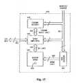
- FIG. 17illustrates a memory device in accordance with an embodiment of the present invention.
- FIG. 18is a block diagram of an electrical system, or processor-based system, utilizing a multistate cell constructed in accordance with the present invention.
- wafer and substrate used in the following descriptioninclude any structure having an exposed surface with which to form the integrated circuit (IC) structure of the invention.
- substrateis understood to include semiconductor wafers.
- substrateis also used to refer to semiconductor structures during processing, and may include other layers that have been fabricated thereupon. Both wafer and substrate include doped and undoped semiconductors, epitaxial semiconductor layers supported by a base semiconductor or insulator, as well as other semiconductor structures well known to one skilled in the art.
- conductoris understood to include semiconductors
- insulatoris defined to include any material that is less electrically conductive than the materials referred to as conductors.
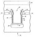
- FIG. 1is a simplified side view, in section, of a semiconductor substrate portion 20 at one stage in processing, in accordance with an embodiment of the present invention.
- the portion 20includes etched or incised recesses 22 , doped regions 24 and 26 and caps 28 .
- the etched recesses 22form trenches extending along an axis into and out of the page of FIG. 1 .
- the doped regions 24are implanted n+regions. In one embodiment, the doped regions 24 are formed by a blanket implant. In one embodiment, the caps 28 are dielectric caps and may be formed using conventional silicon nitride and conventional patterning techniques. In one embodiment, the etched recesses 22 are then etched using conventional plasma etching techniques. In one embodiment, the doped regions 26 are then doped by implantation to form n+regions. The etched or incised recesses 22 may be formed by plasma etching, laser-assisted techniques or any other method presently known or that may be developed. In one embodiment, the recesses 22 are formed to have substantially vertical sidewalls relative to a top surface of the substrate portion 20 . In one embodiment, substantially vertical means at 90 degrees to the substrate surface, plus or minus ten degrees.
- FIG. 2provides a simplified side view, in section, of the substrate portion 20 of FIG. 1 at a later stage in processing, in accordance with an embodiment of the present invention.
- the portion 20 of FIG. 2includes thick oxide regions 32 , ONO regions 34 formed on sidewalls 36 of the recesses 22 , gate material 38 and a conductive layer 40 .
- the gate material 38comprises conductively-doped polycrystalline silicon.
- conventional techniquesare employed to oxidize the doped regions 24 and 26 preferentially with respect to sidewalls 36 .
- the thick oxide regions 32are formed at the same time as a thinner oxide 42 on the sidewalls 36 .
- These oxidesalso serve to isolate the doped regions 24 and 26 from what will become transistor channels along the sidewalls 36 .
- Other techniques for isolationmay be employed.
- high density plasma grown oxidesmay be employed.
- spacersmay be employed.
- conventional techniquesare then employed to provide a nitride layer 44 and an oxide layer 46 , as is described, for example, in “NROM: A Novel Localized Trapping, 2-Bit Nonvolatile Memory Cell”, by Boaz Eitan et al., IEEE Electron Device Letters, Vol. 21, No. 11, November 2000, pp. 543-545, IEEE Catalogue No. 0741-3106/00, or in “A True Single-Transistor Oxide-Nitride-Oxide EEPROM Device” by T. Y. Chan et al., IEEE Electron Device Letters, Vol. EDL-8, No. 3, March, 1987, pp. 93-95, IEEE Catalogue No. 0741-3106/87/0300-0093.
- the thin oxide 42 , nitride layer 44 and oxide layer 46combine to form the ONO layer 34 , such as is employed in SONOS devices, while the polysilicon 38 forms a control gate.
- application of suitable electrical biases to the doped regions 24 , 26 and the control gate 38cause hot majority charge carriers to be injected into the nitride layer 44 and become trapped, providing a threshold voltage shift and thus providing multiple, alternative, measurable electrical states representing stored data.
- Hot charge carriersare not in thermal equilibrium with their environment. In other words, hot charge carriers represent a situation where a population of high kinetic energy charge carriers exist. Hot charge carriers may be electrons or holes.
- SONOS devicesare capable of storing more than one bit per gate 38 .
- the hot carriersare injected into one side 47 or 47 ′ of the ONO layer 34 , adjacent a contact, such as the region 24 or the region 26 , that provides a high electrical field.
- the structure shown in FIG. 2is capable of storing at least four bits per gate 38 .
- FIG. 3is a simplified side view, in section, of the substrate portion 20 of FIG. 1 at an alternative stage in processing, in accordance with an embodiment of the present invention.
- the embodiment shown in FIG. 3includes the oxide regions 32 and 42 , but a floating gate 48 is formed on the thin oxide region 42 .
- a conventional oxide or nitride insulator 49is formed on the floating gate 48 , followed by deposition of gate material 38 .
- Floating gate devicesare known and operate by injecting hot charge carriers, which may comprise electrons or holes, into the floating gate 48 .
- Floating gate devicescan be programmed to different charge levels that can be electrically distinct and distinguishable. As a result, it is possible to program more data than one bit into each floating gate device, and each externally addressable gate 38 thus corresponds to more than one stored bit.
- charge levels of 0, Q, 2Q and 3Qmight be employed, where Q represents some amount of charge corresponding to a reliably-distinguishable output signal.
- FIG. 4is a simplified plan view of a substrate portion showing a portion of a memory cell array 50 , in accordance with an embodiment of the present invention.
- FIG. 4also provides examples of pitch P, width W, space S and minimum feature size F, as described in the Background.
- An exemplary memory cell area 52the physical area of a single transistor, can be seen to be about one F 2 .
- Wordlines 54are formed from the conductive layer 40 , and bitlines 56 and 58 are formed.
- FIG. 5is a simplified side view, in section, illustrating a relationship between the structures of FIGS. 1-3 and the plan view of FIG. 4 , in accordance with an embodiment of the present invention.
- the trenches 22correspond to bitlines 56 and 58 , as is explained below in more detail with reference to FIGS. 6-8 .
- the density of memory arrays such as that described with reference to FIGS. 1-5can require interconnection arrangements that differ from prior art memory arrays.
- One embodiment of a new type of interconnection arrangement useful with such memory systemsis described below with reference to FIGS. 6-8 .
- FIG. 6is a simplified plan view illustrating an interconnection arrangement 60 for the memory cell array 50 of FIG. 4 , in accordance with an embodiment of the present invention.
- the interconnection arrangement 60includes multiple patterned conductive layers 62 and 64 , separated by conventional interlevel dielectric material 65 ( FIGS. 7 and 8 ).
- the views in FIG. 6-8have been simplified to show correspondence with the other Figures and to avoid undue complexity. Shallow trench isolation regions 67 isolate selected portions from one another.
- FIG. 7is a simplified side view, in section, taken along section lines 7 - 7 of FIG. 6 , illustrating part of an interconnection arrangement in accordance with an embodiment of the present invention.
- FIG. 8is a simplified side view, in section, taken along section lines 8 - 8 of FIG. 6 , illustrating part of an interconnection arrangement in accordance with an embodiment of the present invention.
- the patterned conductive layer 62extends upward to nodes 70 , 70 ′, 70 ′′ and establishes electrical communication between the conductive layers 62 and selected portions of the doped region 24 .
- the patterned conductive layer 62stops at the line denoted 72 , 72 ′.
- patterned conductive layer 62extends from the line denoted 74 , 74 ′ and extend upward, providing electrical communication from nodes 76 , 76 ′, 76 ′′ to other circuit elements.
- the nodes 76 , 76 ′, 76 ′′provide contact to selected portions of the doped region 24 .
- patterned conductive layers 64extend from top to bottom of FIG. 6 and electrically couple to nodes 78 , 78 ′′ and thus to doped region 26 .
- FIG. 9Ais useful in illustrating the conventional operation of a MOSFET such as can be used in a DRAM array.
- FIG. 9Aillustrates the normal hot electron injection and degradation of devices operated in the forward direction. As is explained below, since the electrons are trapped near the drain they are not very effective in changing the device characteristics.
- FIG. 9Ais a block diagram of a metal oxide semiconductor field effect transistor (MOSFET) 101 in a substrate 100 .
- the MOSFET 101includes a source region 102 , a drain region 104 , a channel region 106 in the substrate 100 between the source region 102 and the drain region 104 .
- a gate 108is separated from the channel region 108 by a gate oxide 110 .
- a sourceline 112is coupled to the source region 102 .
- a bitline 114is coupled to the drain region 104 .
- a wordline 116is coupled to the gate 108 .
- a drain to source voltage potential(Vds) is set up between the drain region 104 and the source region 102 .
- a voltage potentialis then applied to the gate 108 via a wordline 116 .
- Vtcharacteristic voltage threshold
- a channel 106forms in the substrate 100 between the drain region 104 and the source region 102 . Formation of the channel 106 permits conduction between the drain region 104 and the source region 102 , and a current signal (Ids) can be detected at the drain region 104 .
- FIG. 9Cillustrates this point.
- FIG. 9Cis a graph showing the square root of the current signal (Ids) taken at the drain region versus the voltage potential (VGS) established between the gate 108 and the source region 102 .
- the change in the slope of the plot of ⁇ square root over (Ids) ⁇ versus VGSrepresents the change in the charge carrier mobility in the channel 106 .
- ⁇ VTrepresents the minimal change in the MOSFET's threshold voltage resulting from electrons gradually being trapped in the gate oxide 110 near the drain region 104 , under normal operation, due to device degradation. This results in a fixed trapped charge in the gate oxide 110 near the drain region 104 .
- Slope 1represents the charge carrier mobility in the channel 106 for FIG. 9A having no electrons trapped in the gate oxide 110 .
- Slope 2represents the charge mobility in the channel 106 for the conventional MOSFET of FIG. 9B having electrons 117 trapped in the gate oxide 110 near the drain region 104 .
- slope 1 and slope 2 in FIG. 9Cthe electrons 117 trapped in the gate oxide 110 near the drain region 104 of the conventional MOSFET do not significantly change the charge mobility in the channel 106 .
- One componentincludes a threshold voltage shift due to the trapped electrons and a second component includes mobility degradation due to additional scattering of carrier electrons caused by this trapped charge and additional surface states.
- a conventional MOSFETdegrades, or is “stressed,” over operation in the forward direction, electrons do gradually get injected and become trapped in the gate oxide near the drain. In this portion of the conventional MOSFET there is virtually no channel underneath the gate oxide. Thus the trapped charge modulates the threshold voltage and charge mobility only slightly.
- Applicanthas previously described programmable memory devices and functions based on the reverse stressing of MOSFET's in a conventional CMOS process and technology in order to form programmable address decode and correction. (See generally, L. Forbes, W. P. Noble and E. H. Cloud, “MOSFET technology for programmable address decode and correction,” U.S. patent application Ser. No. 09/383,804). That disclosure, however, did not describe multistate memory cell solutions, but rather address decode and correction issues.
- normal MOSFETscan be programmed by operation in the reverse direction and utilizing avalanche hot electron injection to trap electrons in the gate oxide of the MOSFET.
- the programmed MOSFETis subsequently operated in the forward direction the electrons trapped in the oxide are near the source and cause the channel to have two different threshold voltage regions.
- the novel programmed MOSFETs of the present inventionconduct significantly less current than conventional MOSFETs, particularly at low drain voltages. These electrons will remain trapped in the gate oxide unless negative gate voltages are applied. The electrons will not be removed from the gate oxide when positive or zero gate voltages are applied.
- Erasurecan be accomplished by applying negative gate voltages and/or increasing the temperature with negative gate bias applied to cause the trapped electrons to be re-emitted back into the silicon channel of the MOSFET.
- negative gate voltagesSee generally, L. Forbes, E. Sun, R. Alders and J. Moll, “Field induced re-emission of electrons trapped in SiO 2 ,” IEEE Trans. Electron Device, vol. ED-26, no. 11, pp. 1816-1818 (November 1979); S. S. B. Or, N. Hwang, and L. Forbes, “Tunneling and Thermal emission from a distribution of deep traps in SiO 2 ,” IEEE Trans. on Electron Devices, vol. 40, no. 6, pp. 1100-1103 (June 1993); S. A. Abbas and R. C. Dockerty, “N-channel IGFET design limitations due to hot electron trapping,” IEEE Int. Electron Devices Mtg., Washington D.C., December 1975, pp. 35-38).
- FIGS. 10A-10Care useful in illustrating the present invention in which a much larger change in device characteristics is obtained by programming the device in the reverse direction and subsequently reading the device by operating it in the forward direction.
- FIG. 10Ais a diagram of a programmed MOSFET which can be used as a multistate cell according to the teachings of the present invention.
- the multistate cell 201includes a MOSFET in a substrate 200 which has a first source/drain region 202 , a second source/drain region 204 , and a channel region 206 between the first and second source/drain regions, 202 and 204 .
- the first source/drain region 202includes a source region 202 for the MOSFET and the second source/drain region 204 includes a drain region 204 for the MOSFET.
- FIG. 10Afurther illustrates a gate 208 separated from the channel region 206 by a gate oxide 210 .
- a first transmission line 212is coupled to the first source/drain region 202 and a second transmission line 214 is coupled to the second source/drain region 204 .
- the first transmission lineincludes a sourceline 212 and the second transmission line includes a bit line 214 .
- multistate cell 201is comprised of a programmed MOSFET.
- This programmed MOSFEThas a charge 217 trapped in the gate oxide 210 adjacent to the first source/drain region 202 such that the channel region 206 has a first voltage threshold region (Vt 1 ) and a second voltage threshold region (Vt 2 ) in the channel 206 .
- the charge 217 trapped in the gate oxide 210 adjacent to the first source/drain region 202includes a trapped electron charge 217 .
- the multistate cellcan be programmed to have one of a number of charge levels trapped in the gate insulator adjacent to the first source/drain region 202 such that the channel region 206 will have a first voltage threshold region (Vt 1 ) and a second voltage threshold region (Vt 2 ) and such that the programmed multistate cell operates at reduced drain source current.
- Vt 1first voltage threshold region
- Vt 2second voltage threshold region
- FIG. 10Aillustrates the Vt 2 in the channel 206 is adjacent the first source/drain region 202 and that the Vt 1 in the channel 206 is adjacent the second source/drain region 204 .
- Vt 2has a higher voltage threshold than Vt 1 due to the charge 217 trapped in the gate oxide 217 adjacent to the first source/drain region 202 .
- Multiple bitscan be stored on the multistate cell 201 .
- FIG. 10Bis a diagram suitable for explaining the method by which the MOSFET of the multistate cell 201 of the present invention can be programmed to achieve the embodiments of the present invention.
- the methodincludes programming the MOSFET in a reverse direction.
- Programming the MOSFET in the reverse directionincludes applying a first voltage potential V 1 to a drain region 204 of the MOSFET.
- applying a first voltage potential V 1 to the drain region 204 of the MOSFETincludes grounding the drain region 204 of the MOSFET as shown in FIG. 10B .
- a second voltage potential V 2is applied to a source region 202 of the MOSFET.
- applying a second voltage potential V 2 to the source region 202includes applying a high positive voltage potential (VDD) to the source region 202 of the MOSFET, as shown in FIG. 10B .
- a gate potential VGSis applied to a gate 208 of the MOSFET.
- the gate potential VGSincludes a voltage potential which is less than the second voltage potential V 2 , but which is sufficient to establish conduction in the channel 206 of the MOSFET between the drain region 204 and the source region 202 . As shown in FIG.
- applying the first, second and gate potentials (V 1 , V 2 , and VGS respectively) to the MOSFETcreates a hot electron injection into a gate oxide 210 of the MOSFET adjacent to the source region 202 .
- applying the first, second and gate potentials (V 1 , V 2 , and VGS respectively)provides enough energy to the charge carriers, e.g. electrons, being conducted across the channel 206 that, once the charge carriers are near the source region 202 , a number of the charge carriers get excited into the gate oxide 210 adjacent to the source region 202 .
- the charge carriersbecome trapped.
- the methodis continued by subsequently operating the MOSFET in the forward direction in its programmed state during a read operation.
- the read operationincludes grounding the source region 202 and precharging the drain region a fractional voltage of VDD. If the device is addressed by a wordline coupled to the gate, then its conductivity will be determined by the presence or absence of stored charge in the gate insulator. That is, a gate potential can be applied to the gate 208 by a wordline 216 in an effort to form a conduction channel between the source and the drain regions as done with addressing and reading conventional DRAM cells.
- the conduction channel 206 of the MOSFETwill have a first voltage threshold region (Vt 1 ) adjacent to the drain region 204 and a second voltage threshold region (Vt 2 ) adjacent to the source region 202 , as explained and described in detail in connection with FIG. 10A .
- the Vt 2has a greater voltage threshold than the Vt 1 due to the hot electron injection 217 into a gate oxide 210 of the MOSFET adjacent to the source region 202 .
- FIG. 10Cis a graph plotting a current signal (Ids) detected at the second source/drain region 204 versus a voltage potential, or drain voltage, (VDS) set up between the second source/drain region 204 and the first source/drain region 202 (Ids vs. VDS).
- VDSrepresents the voltage potential set up between the drain region 204 and the source region 202 .
- the curve plotted as D 1represents the conduction behavior of a conventional MOSFET which is not programmed according to the teachings of the present invention.
- the curve D 2represents the conduction behavior of the programmed MOSFET, described above in connection with FIG. 10A , according to the teachings of the present invention. As shown in FIG.
- the current signal (IDS 2 ) detected at the second source/drain region 204 for the programmed MOSFET (curve D 2 )is significantly lower than the current signal (IDS 1 ) detected at the second source/drain region 204 for the conventional MOSFET which is not programmed according to the teachings of the present invention.
- the channel 206 in the programmed MOSFET of the present inventionhas two voltage threshold regions and that the voltage threshold, Vt 2 , near the first source/drain region 202 has a higher voltage threshold than Vt 1 near the second source/drain region due to the charge 217 trapped in the gate oxide 217 adjacent to the first source/drain region 202 .
- NROMNonvolatile Memory Cell
- B. Eitan et al.“Characterization of Channel Hot Electron Injection by the Subthreshold Slope of NROM device,” IEEE Electron Device Lett., Vol. 22, No. 11, pp. 556-558, (November 2001); B. Etian et al., “NROM: A novel localized Trapping, 2-Bit Nonvolatile Memory Cell,” IEEE Electron Device Lett., Vol. 21, No. 11, pp. 543-545, (November 2000)).
- Charge trapping in silicon nitride gate insulatorswas the basic mechanism used in MNOS memory devices (see generally, S. Sze, Physics of Semiconductor Devices, Wiley, N.Y., 1981, pp. 504-506), charge trapping in aluminum oxide gates was the mechanism used in MIOS memory devices (see generally, S. Sze, Physics of Semiconductor Devices, Wiley, N.Y., 1981, pp. 504-506), and Applicant has previously disclosed charge trapping at isolated point defects in gate insulators (see generally, L. Forbes and J. Geusic, “Memory using insulator traps,” U.S. Pat. No. 6,140,181, issued Oct. 31, 2000).
- the present inventiondiscloses programming a MOSFET in a reverse direction to trap one of a number of charge levels near the source region and reading the device in a forward direction to form a multistate memory cell based on a modification of DRAM technology.
- Prior art DRAM technologygenerally employs silicon oxide as the gate insulator. Further the emphasis in conventional DRAM devices is placed on trying to minimize charge trapping in the silicon oxide gate insulator. According to the teachings of the present invention, a variety of insulators are used to trap electrons more efficiently than in silicon oxide. That is, in the present invention, the multistate memory cell employs charge trapping in gate insulators such as, wet silicon oxide, silicon nitride, silicon oxynitride SON, silicon rich oxide SRO, aluminum oxide Al 2 O 3 , composite layers of these insulators such as oxide and then silicon nitride, or oxide and then aluminum oxide, or multiple layers as oxide-nitride-oxide. While the charge trapping efficiency of silicon oxide may be low such is not the case for silicon nitride or composite layers of silicon oxide and nitride.
- FIG. 11illustrates a portion of a memory array 300 according to the teachings of the present invention.
- the memory in FIG. 11is shown illustrating a number of vertical pillars, or multistate cells, 301 - 1 and 301 - 2 formed according to the teachings of the present invention.
- the number of vertical pillarsare formed in rows and columns extending outwardly from a substrate 303 .
- the number of vertical pillars, 301 - 1 and 301 - 2are separated by a number of trenches 340 .
- the number of vertical pillars, 301 - 1 and 301 - 2serve as transistors including a first source/drain region, 302 - 1 and 302 - 2 , respectively.
- the first source/drain region, 302 - 1 and 302 - 2is coupled to a sourceline 304 .
- the sourceline 304is formed in a bottom of the trenches 340 between rows of the vertical pillars, 301 - 1 and 301 - 2 .
- the sourceline 304is formed from a doped region implanted in the bottom of the trench.
- a second source/drain region, 306 - 1 and 306 - 2 respectively,is coupled to a bitline (not shown).
- a channel region 305is located between the first and the second source/drain regions.
- a gate 309is separated from the channel region 305 by a gate insulator 307 in the trenches 340 along rows of the vertical pillars, 301 - 1 and 301 - 2 .
- the gate insulator 307includes a gate insulator 307 selected from the group of silicon dioxide (SiO 2 ) formed by wet oxidation, silicon oxynitride (SON), silicon rich oxide (SRO), and aluminum oxide (Al 2 O 3 ).
- the gate insulator 307includes a gate insulator 307 selected from the group of silicon rich aluminum oxide insulators, silicon rich oxides with inclusions of nanoparticles of silicon, silicon oxide insulators with inclusions of nanoparticles of silicon carbide, and silicon oxycarbide insulators.
- the gate insulator 307includes a composite layer 307 .
- the composite layer 307includes a composite layer 307 selected from the group of an oxide-aluminum oxide (Al 2 O 3 )-oxide composite layer, and oxide-silicon oxycarbide-oxide composite layer.
- the composite layer 307includes a composite layer 307 , or a non-stoichiometric single layer, of two or more materials selected from the group of silicon (Si), titanium (Ti), and tantalum (Ta).
- the gate insulator 307includes an oxide-nitride-oxide (ONO) gate insulator 307 .
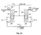
- FIG. 12illustrates an electrical equivalent circuit 400 for the portion of the memory array shown in FIG. 11 .
- a number of vertical multistate cells, 401 - 1 and 401 - 2are provided.
- Each vertical multistate cell, 401 - 1 and 401 - 2includes a first source/drain region, 402 - 1 and 402 - 2 , a second source/drain region 406 - 1 and 406 - 2 , a channel region 405 between the first and the second source/drain regions, and a gate 409 separated from the channel region by a gate insulator 407 .
- FIG. 12further illustrates a number of bit lines, 411 - 1 and 411 - 2 , coupled to the second source/drain region 406 - 1 and 406 - 2 of each multistate cell.
- the number of bit lines, 411 - 1 and 411 - 2are coupled to the second source/drain region 406 - 1 and 406 - 2 along rows of the memory array.
- a number of word lines, such as wordline 413 in FIG. 12are coupled to the gate 409 of each multistate cell along columns of the memory array.
- a number of sourcelines, such as common sourceline 415are coupled to the first source/drain regions, e.g.
- column adjacent pillarsinclude a transistor which operates as a vertical multistate cell, e.g. 401 - 1 , on one side of a shared trench, the shared trench separating rows of the pillars as described in connection with FIG. 11 , and a transistor which operates as a reference cell, e.g. 401 - 2 , having a programmed conductivity state on the opposite side of the shared trench.
- At least one of multistate cellscan be programmed to have one of a number of charge levels trapped in the gate insulator, shown generally as 417 , adjacent to the first source/drain region, e.g. 402 - 1 , such that the channel region 405 will have a first voltage threshold region (Vt 1 ) and a second voltage threshold region (Vt 2 ) and such that the programmed multistate cell operates at reduced drain source current.
- Vt 1first voltage threshold region
- Vt 2second voltage threshold region
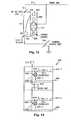
- FIG. 13is another electrical equivalent circuit useful in illustrating a read operation on the novel multistate cell 500 according to the teachings of the present invention.
- the electrical equivalent circuit in FIG. 13represents a programmed vertical multistate cell.
- the programmed vertical multistate cell 500includes a vertical metal oxide semiconductor field effect transistor (MOSFET) 500 extending outwardly from a substrate.
- the MOSFEThas a source region 502 , a drain region 506 , a channel region 505 between the source region 502 and the drain region 506 , and a gate 509 separated from the channel region 505 by a gate insulator, shown generally as 507 .
- MOSFETvertical metal oxide semiconductor field effect transistor
- a wordline 513is coupled to the gate 509 .
- a sourceline 504formed in a trench adjacent to the vertical MOSFET as described in connection with FIG. 11 , is coupled to the source region 502 .
- a bit line, or data line 511is coupled to the drain region 506 .
- the multistate cell 500 shown in FIG. 13is an example of a programmed multistate cell 500 having one of a number of charge levels trapped in the gate insulator, shown generally as 517 , adjacent to the first source/drain region, 502 , such that the channel region 505 will have a first voltage threshold region (Vt 1 ) and a second voltage threshold region (Vt 2 ) and such that the programmed multistate cell 500 operates at reduced drain source current.
- the second voltage threshold region (Vt 2 )is now a high voltage threshold region which is greater than the first voltage threshold region (Vt 1 ).
- FIG. 14illustrates a portion of a memory array 600 according to the teachings of the present invention.
- the memory in FIG. 14is shown illustrating a pair of multistate cells 601 - 1 and 601 - 2 formed according to the teachings of the present invention.
- any number of multistate cellscan be organized in an array, but for ease of illustration only two are displayed in FIG. 14 .
- a first source/drain region, 602 - 1 and 602 - 2 respectivelyis coupled to a sourceline 604 .
- a second source/drain region, 606 - 1 and 606 - 2 respectively,is coupled to a bitline, 608 - 1 and 608 - 2 respectively.
- Each of the bitlines, 608 - 1 and 608 - 2couple to a sense amplifier, shown generally at 610 .
- a wordline, 612 - 1 and 612 - 2 respectivelyis couple to a gate, 614 - 1 and 614 - 2 respectively, for each of the multistate cells, 601 - 1 and 601 - 2 .
- the wordlines, 612 - 1 and 612 - 2run across or are perpendicular to the rows of the memory array 600 .
- a write data/precharge circuitis shown at 624 for coupling a first or a second potential to bitline 608 - 1 .
- the write data/precharge circuit 624is adapted to couple either a ground to the bitline 608 - 1 during a write operation in the reverse direction, or alternatively to precharge the bitline 608 - 1 to fractional voltage of VDD during a read operation in the forward direction.
- the sourceline 604can be biased to a voltage higher than VDD during a write operation in the reverse direction, or alternatively grounded during a read operation in the forward direction.
- the array structure 600including multistate cells 601 - 1 and 601 - 2 , has no capacitors.
- the first source/drain region or source region, 602 - 1 and 602 - 2are coupled directly to the sourceline 604 .
- the sourceline 604is biased to voltage higher than VDD and the devices stressed in the reverse direction by grounding the data or bit line, 608 - 1 or 608 - 2 .
- the multistate cell, 601 - 1 or 601 - 2is selected by a word line address, 612 - 1 or 612 - 2 , then the multistate cell, 601 - 1 or 601 - 2 , will conduct and be stressed with accompanying hot electron injection into the cells gate insulator adjacent to the source region, 602 - 1 or 602 - 2 .
- a number of different charge levelscan be programmed into the gate insulator adjacent to source region such that the cells is used as a differential cell and/or the cell is compared to a reference or dummy cell, as shown in FIG. 14 , and multiple bits can be stored on the multistate cell.
- the multistate cell, 601 - 1 or 601 - 2is operated in the forward direction with the sourceline 604 grounded and the bit line, 608 - 1 or 608 - 2 , and respective second source/drain region or drain region, 606 - 1 and 606 - 2 , of the cells precharged to some fractional voltage of Vdd. If the device is addressed by the word line, 612 - 1 or 612 - 2 , then its conductivity will be determined by the presence or absence of the amount of stored charge trapped in the gate insulator as measured or compared to the reference or dummy cell and so detected using the sense amplifier 610 .
- the operation of DRAM sense amplifiersis described, for example, in U.S. Pat. Nos.
- the devicesIn operation the devices would be subjected to hot electron stress in the reverse direction by biasing the sourceline 604 , and read while grounding the sourceline 604 to compare a stressed multistate cell, e.g. cell 601 - 1 , to an unstressed dummy device/cell, e.g. 601 - 2 , as shown in FIG. 14 .
- the write and possible erase featurecould be used during manufacture and test to initially program all cells or devices to have similar or matching conductivity before use in the field.
- the transistors in the reference or dummy cells, e.g. 601 - 2can all initially be programmed to have the same conductivity states.
- the sense amplifier 610can then detect small differences in cell or device characteristics due to stress induced changes in device characteristics during the write operation.
- a gate insulator of the multistate cellincludes gate insulators selected from the group of thicker layers of SiO 2 formed by wet oxidation, SON silicon oxynitride, SRO silicon rich oxide, Al 2 O 3 aluminum oxide, composite layers and implanted oxides with traps (L. Forbes and J. Geusic, “Memory using insulator traps,” U.S. Pat. No. 6,140,181, issued Oct. 31, 2000).
- Conventional transistors for address decode and sense amplifierscan be fabricated after this step with normal thin gate insulators of silicon oxide.
- FIGS. 15A-15B and 16 A- 16 Bare useful in illustrating the use of charge storage in the gate insulator to modulate the conductivity of the multistate cell according to the teachings of the present invention. That is, FIGS. 15A-16B illustrate the operation of the novel multistate cell 701 formed according to the teachings of the present invention.
- the gate insulator 707has a number of layers, e.g. an ONO stack, where layer 707 A is the oxide layer closest to the channel 705 and a nitride layer 707 B is formed thereon.
- the oxide layer 707 Ais illustrated having a thickness of approximately 6.7 nm or 67 ⁇ (roughly 10 ⁇ 6 cm).
- a multistate cellhaving dimensions of 0.1 ⁇ m (10 ⁇ 5 cm) by 0.1 ⁇ m.
- the charge storage region near the sourcecan reasonably have dimensions of 0.1 micron (1000 ⁇ ) by 0.02 micron (200 ⁇ ) in a 0.1 micron technology. If the gate oxide 707 A nearest the channel 705 is 67 ⁇ then a charge of 100 electrons will cause a threshold voltage shift in this region of 1.6 Volts since the oxide capacitance is about 0.5 micro-Farad ( ⁇ F) per square centimeter.
- the transistorhas a total effective oxide thickness of 200 ⁇ then a change in the threshold voltage of only 0.16 Volts near the source, corresponding to 10 electrons, is estimated to change the transistor current by 4 micro Amperes ( ⁇ A).
- the sense amplifier described in connection with FIG. 14which is similar to a DRAM sense amplifier, can easily sense this charge difference on the data or bitlines.
- the sensed charge difference on the data or bitlineswill be 40 femto Coulombs (fC) over a sense period of 10 nano seconds (nS).
- the programmed multistate cell, or modified MOSFETis a programmed MOSFET having a charge trapped in the gate insulator adjacent to a first source/drain region, or source region, such that the channel region has a first voltage threshold region (Vt 1 ) and a second voltage threshold region (Vt 2 ), where Vt 2 is greater than Vt 1 , and Vt 2 is adjacent the source region such that the programmed MOSFET operates at reduced drain source current.
- Vt 1first voltage threshold region
- Vt 2second voltage threshold region
- the sense amplifier described in connection with FIG. 14which is similar to a DRAM sense amplifier, can easily sense this charge difference on the data or bitlines.
- the sensed charge difference on the data or bitlineswill be 40 femto Coulombs (fC) over a sense period of 10 nano seconds (nS) for this representative one of a number of stored charge levels according to the teachings of the present invention.
- fCfemto Coulombs
- nSnano seconds
- a number of different charge levelscan be programmed into the gate insulator adjacent to source region such that the cell is used as a differential cell and/or the cell is compared to a reference or dummy cell, as shown in FIG. 14 , and multiple bits can be stored on the multistate cell of the present invention.
- FIG. 15Baids to further illustrate the conduction behavior of the novel multistate cell of the present invention.
- the electrical equivalent circuit shown in FIG. 15Billustrates a multistate cell 701 having an equivalent oxide thickness of 200 ⁇ .
- this drain current IDcorresponds to 10 electrons trapped in the gate insulator, or charge storage region 707 near the source 702 .
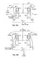
- FIG. 16A and 16Billustrate the operation and programming the novel multistate cell as described above.
- FIGS. 16A and 16Balso help illustrate an alternative array configuration where adjacent devices are compared and one of the devices on the opposite side of a shared trench is used as a dummy cell transistor or reference device. Again, the reference devices can all be programmed to have the same initial conductivity state.
- FIG. 16Aillustrates the operation and programming the novel multistate cell in the reverse direction. As shown in FIG. 16A , a transistor 801 - 1 on one side of the trench (as described in connection with FIG. 11 ) is stressed by grounding its respective drain line, e.g. 811 - 1 . As shown in FIG.
- the drain line 811 - 2 for the transistor 801 - 2 on the opposite side of the trenchis left floating.
- a voltageis applied to the shared sourceline 804 located at the bottom of the trench (as described in connection with FIG. 11 ) which now acts as a drain.
- the neighboring (shared trench)/column adjacent transistors, 801 - 1 and 801 - 2share a gate 807 and the wordline 813 , e.g. polysilicon gate lines, coupling thereto run across or are perpendicular to the rows containing the bit and source lines, e.g. 811 - 1 , 811 - 2 , and 804 .
- a gate voltageis applied to the gates 807 .
- the multistate cell 801 - 1will conduct and be stressed with accompanying hot electron injection into the cells gate insulator 817 adjacent to the source region 802 - 1 .
- FIG. 16Billustrates the now programmed multistate cell's operation in the forward direction and differential read occurring in a this differential cell embodiment, e.g. 2 transistors in each cell.
- the drain and sourceor ground
- the drain line, 811 - 1 and 811 - 2have the normal forward direction potential applied thereto.
- the shared sourceline 804 located at the bottom of the trench(as described in connection with FIG. 11 ) is grounded and once again acts as a source. And, a gate voltage is applied to the gates 807 .
- these novel multistate cellscan be used in a DRAM like array.
- Each transistorcan now, however, store many bits so the data storage density is much higher than one bit for each 1F squared unit area.
- Using a reference or dummy cell for each memory transistor where the reference transistor is in close proximitye.g. the embodiment shown in FIGS. 16A and 16B vs. that shown in FIG. 12 , results in better matching characteristics of transistors, but a lower memory density.
- the memory device 940contains a memory array 942 , row and column decoders 944 , 948 and a sense amplifier circuit 946 .
- the memory array 942consists of a plurality of multistate cells 900 , formed according to the teachings of the present invention whose word lines 980 and bit lines 960 are commonly arranged into rows and columns, respectively.
- the bit lines 960 of the memory array 942are connected to the sense amplifier circuit 946 , while its word lines 980 are connected to the row decoder 944 .
- Address and control signalsare input on address/control lines 961 into the memory device 940 and connected to the column decoder 948 , sense amplifier circuit 946 and row decoder 944 and are used to gain read and write access, among other things, to the memory array 942 .
- the column decoder 948is connected to the sense amplifier circuit 946 via control and column select signals on column select lines 962 .
- the sense amplifier circuit 946receives input data destined for the memory array 942 and outputs data read from the memory array 942 over input/output (I/O) data lines 963 .
- Datais read from the cells of the memory array 942 by activating a word line 980 (via the row decoder 944 ), which couples all of the memory cells corresponding to that word line to respective bit lines 960 , which define the columns of the array.
- One or more bit lines 960are also activated.
- the sense amplifier circuit 946 connected to a bit line columndetects and amplifies the conduction sensed through a given multistate cell, where in the read operation the source region of a given cell is couple to a grounded array plate (not shown), and transferred its bit line 960 by measuring the potential difference between the activated bit line 960 and a reference line which may be an inactive bit line.
- the operation of Memory device sense amplifiersis described, for example, in U.S. Pat. Nos. 5,627,785; 5,280,205; and 5,042,011, all assigned to Micron Technology Inc., and incorporated by reference herein.
- FIG. 18is a block diagram of an electrical system, or processor-based system, 1000 utilizing multistate memory cells 1012 constructed in accordance with the present invention. That is, the multistate memory cells 1012 utilizes the modified DRAM cell as explained and described in detail in connection with FIGS. 2-4 .
- the processor-based system 1000may be a computer system, a process control system or any other system employing a processor and associated memory.
- the system 1000includes a central processing unit (CPU) 1002 , e.g., a microprocessor, that communicates with the multistate memory 1012 and an I/O device 1008 over a bus 1020 .
- CPUcentral processing unit
- the bus 1020may be a series of buses and bridges commonly used in a processor-based system, but for convenience purposes only, the bus 1020 has been illustrated as a single bus.
- a second I/O device 1010is illustrated, but is not necessary to practice the invention.
- the processor-based system 1000can also includes read-only memory (ROM) 1014 and may include peripheral devices such as a floppy disk drive 1004 and a compact disk (CD) ROM drive 1006 that also communicates with the CPU 1002 over the bus 1020 as is well known in the art.
- ROMread-only memory
- CDcompact disk
- At least one of the multistate cell in NROM 1012includes a programmed MOSFET having a charge trapped in the gate insulator adjacent to a first source/drain region, or source region, such that the channel region has a first voltage threshold region (Vt 1 ) and a second voltage threshold region (Vt 2 ), where Vt 2 is greater than Vt 1 , and Vt 2 is adjacent the source region such that the programmed MOSFET operates at reduced drain source current.
- Vt 1first voltage threshold region
- Vt 2second voltage threshold region
- FIG. 18illustrates an embodiment for electronic system circuitry in which the novel memory cells of the present invention are used.
- the illustration of system 1000is intended to provide a general understanding of one application for the structure and circuitry of the present invention, and is not intended to serve as a complete description of all the elements and features of an electronic system using the novel memory cell structures.
- the inventionis equally applicable to any size and type of memory device 1000 using the novel memory cells of the present invention and is not intended to be limited to that described above.
- such an electronic systemcan be fabricated in single-package processing units, or even on a single semiconductor chip, in order to reduce the communication time between the processor and the memory device.
- Applications containing the novel memory cell of the present invention as described in this disclosureinclude electronic systems for use in memory modules, device drivers, power modules, communication modems, processor modules, and application-specific modules, and may include multilayer, multichip modules.
- Such circuitrycan further be a subcomponent of a variety of electronic systems, such as a clock, a television, a cell phone, a personal computer, an automobile, an industrial control system, an aircraft, and others.
- Utilization of a modification of well established DRAM technology and arrayswill serve to afford an inexpensive memory device which can be regarded as disposable if the information is later transferred to another medium, for instance CDROM's.
- the high density of DRAM array structureswill afford the storage of a large volume of digital data or images at a very low cost per bit.
- the low cost of these memorieswill make it more efficient to just utilize a new memory array, and dispose of the old memory array, rather than trying to erase and reuse these arrays as is done with current flash memories.
- the novel multistate cellscan be used in a DRAM like array.
- Using a reference or dummy cell for each memory transistor where the reference transistor is in close proximitye.g., the embodiment shown in FIGS. 16A and 16B vs. that shown in FIG. 12 , results in better matching characteristics of transistors, but a lower memory density.
Landscapes
- Engineering & Computer Science (AREA)
- Microelectronics & Electronic Packaging (AREA)
- Computer Hardware Design (AREA)
- Semiconductor Memories (AREA)
- Non-Volatile Memory (AREA)
Abstract
Description
- This application is a continuation of U.S. patent application Ser. No. 10/738,408 filed Dec. 16, 2003 which is commonly assigned and incorporated herein by reference in their entirety.
- This invention relates to a NROM memory cells, arrays of such memory cells, electronic devices employing such memory cells and arrays, and methods related to such memory cells.
- Various types of memory devices are used in electronic systems. Some types of memory device, such as DRAM (dynamic random access memory) provide large amounts of readable and writable data storage with modest power budget and in favorably small form factor, but are not as fast as other types of memory devices and provide volatile data storage capability. Volatile data storage means that the memory must be continuously powered in order to retain data, and the stored data are lost when the power is interrupted. Nonvolatile memories are capable of retaining data without requiring electrical power.
- Other types of memory can provide read-only or read-write capabilities and non-volatile data storage, but are much slower in operation. These include CD-ROM devices, CD-WORM devices, magnetic data storage devices (hard discs, floppy discs, tapes and so forth), magneto-optical devices and the like.
- Still other types of memory provide very high speed operation but also demand high power budgets. Static RAM or SRAM is an example of such memory devices.
- In most computer systems, different memory types are blended to selectively gain the benefits that each technology can offer. For example, read-only memories or ROM, EEPROM and the like are typically used to store limited amounts of relatively infrequently-accessed data such as a basic input-output system. These memories are employed to store data that, in response to a power ON situation, configure a processor to be able to load larger amounts of software such as an operating system from a high capacity non-volatile memory device such as a hard drive. The operating system and application software are typically read from the high capacity memory and corresponding images are stored in DRAM.
- As the processor executes instructions, some types of data may be repeatedly fetched from memory. As a result, some SRAM or other high speed memory is typically provided as “cache” memory in conjunction with the processor and may be included on the processor integrated circuit or chip and/or very near it.
- Several different kinds of memory device are involved in most modem computing devices, and in many types of appliances that include automated and/or programmable features (home entertainment devices, telecommunications devices, automotive control systems etc.). As system and software complexity increase, need for additional memory increases. Desire for portability, computation power and/or practicality result in increased pressure to reduce both power consumption and circuit area per bit.
- DRAMs have been developed to very high capacities in part because the memory cells can be manufactured to have a very small area, and the power draw per cell can also be made quite small. In turn, this allows memory integrated circuits to be made that incorporate millions of memory cells in each chip. Typical one-transistor, one-capacitor DRAM memory cells can be produced to have extremely small areal requirements.
- Such areas are often equal to about 3F×2F, or less, where “F” is defined as equal to one-half of minimum pitch (see
FIG. 4 , infra). Minimum pitch (i.e., “P”) is defined as equal to the smallest distance of a line width (i.e., “W”) plus width of a space immediately adjacent the line on one side of the line between the line and a next adjacent line in a repeated pattern within the array (i.e., “S”). Thus, in many implementations, the consumed area of a given DRAM cell is no greater than about 8F2. - However, because DRAMs are volatile memory devices, they require “refresh” operations. In a refresh operation, data are read out of each memory cell, amplified and written back into the DRAM. As a first result, the DRAM circuit is usually not available for other kinds of memory operations during the refresh operation. Additionally, refresh operations are carried out periodically, resulting in times during which data cannot be readily extracted from or written to DRAMs. As a second result, some amount of electrical power is always needed to store data in DRAM devices.
- As a third result, boot operations for computers such as personal computers involve a period during which the computer cannot be used following power ON initiation. During this period, operating system instructions and associated data, and application instructions and associated data, are read from relatively slow, non-volatile memory, such as a conventional disc drive, are decoded by the processing unit and the resultant instructions and associated data are loaded into modules incorporating relatively rapidly-accessible, but volatile, memory such as DRAM. Other consequences flow from the properties of the memory systems included in various electronic devices and the increasingly complex software employed with them, however, these examples serve to illustrate ongoing needs.
- Needed are methods and apparatus relating to non-volatile memory providing high areal data storage capacity, reprogrammability, low power consumption and relatively high data access speed.
- In a first aspect, the present invention includes a method for making an array of memory cells configured to store at least one bit per one F2. The method includes doping a first region of a semiconductor substrate and incising the substrate to provide an array of substantially vertical edge surfaces. Pairs of the edge surfaces face one another and are spaced apart a distance equal to one half of a pitch of the array of edges. The method also includes doping second regions between the pairs of edge surfaces and disposing respective structures each providing an electronic memory function on at least some respective ones of the edge surfaces. The method also includes establishing electrical contacts to the first and second regions.
- In another aspect, the present invention includes a method for making an array of memory cells configured to store at least one bit per one F2. The method includes disposing substantially vertical structures providing an electronic memory function spaced apart a distance equal to one half of a minimum pitch of the array and establishing electrical contacts to memory cells including the vertical structures.
- In a further aspect, the present invention includes an array of memory cells configured to store at least one bit per one F2formed using vertical structures providing an electronic memory function spaced apart a distance equal to one half of a minimum pitch of the array. The structures providing the electronic memory function are configured to store more than one bit per gate. The array also includes electrical contacts to the memory cells including the vertical structures.
- In a still further aspect, the present invention includes a vertical metal oxide semiconductor field effect transistor (MOSFET) extending outwardly from a substrate, the MOSFET having a first source/drain region, a second source/drain region, a channel region between the first and the second source/drain regions, and a gate separated from the channel region by a gate insulator. A sourceline is formed in a trench adjacent to the vertical MOSFET, wherein the first source/drain region is coupled to the sourceline. A transmission line is coupled to the second source/drain region. The can be programmed MOSFET to have one of a number of charge levels trapped in the gate insulator adjacent to the first source/drain region such that the channel region has a first voltage threshold region (Vt1) and a second voltage threshold region (Vt2) and such that the programmed MOSFET operates at reduced drain source current.
- These and other embodiments, aspects, advantages, and features of the present invention will be set forth in part in the description which follows, and in part will become apparent to those skilled in the art by reference to the following description of the invention and referenced drawings or by practice of the invention. The aspects, advantages, and features of the invention are realized and attained by means of the instrumentalities, procedures, and combinations particularly pointed out in the appended claims.
- Embodiments of the invention are described below with reference to the following accompanying drawings.
FIG. 1 is a simplified side view, in section, of a semiconductor substrate portion at one stage in processing, in accordance with an embodiment of the present invention.FIG. 2 is a simplified side view, in section, of the substrate portion ofFIG. 1 at a later stage in processing, in accordance with an embodiment of the present invention.FIG. 3 is a simplified side view, in section, of the substrate portion ofFIG. 2 at a later stage in processing, in accordance with an embodiment of the present invention.FIG. 4 is a simplified plan view of a substrate portion showing a portion of a memory cell array, in accordance with an embodiment of the present invention.FIG. 5 is a simplified side view, in section, illustrating a relationship between the structures ofFIGS. 1-3 and the plan view ofFIG. 4 , in accordance with an embodiment of the present invention.FIG. 6 is a simplified plan view of a memory cell array illustrating an interconnection arrangement for the memory cell array ofFIG. 4 , in accordance with an embodiment of the present invention.FIG. 7 is a simplified side view, in section, taken along section lines7-7 ofFIG. 6 , illustrating part of an interconnection arrangement in accordance with an embodiment of the present invention.FIG. 8 is a simplified side view, in section, taken along section lines8-8 ofFIG. 6 , illustrating part of an interconnection arrangement in accordance with an embodiment of the present invention.FIG. 9A is a block diagram of a metal oxide semiconductor field effect transistor (MOSFET) in a substrate according to the teachings of the prior art.FIG. 9B illustrates the MOSFET ofFIG. 9A operated in the forward direction showing some degree of device degradation due to electrons being trapped in the gate oxide near the drain region over gradual use.FIG. 9C is a graph showing the square root of the current signal (Ids) taken at the drain region of the conventional MOSFET versus the voltage potential (VGS) established between the gate and the source region.FIG. 10A is a diagram of a programmed MOSFET which can be used as a multistate cell in accordance with an embodiment of the present invention.FIG. 10B is a diagram suitable for explaining the method by which the MOSFET of the multistate cell of the present invention can be programmed to achieve the embodiments of the present invention.FIG. 10C is a graph plotting the current signal (Ids) detected at the drain region versus a voltage potential, or drain voltage, (VDS) set up between the drain region and the source region (Ids vs. VDS) in accordance with an embodiment of the present invention.FIG. 11 illustrates a portion of a memory array in accordance with an embodiment of the present invention.FIG. 12 illustrates an electrical equivalent circuit for the portion of the memory array shown inFIG. 11 .FIG. 13 is another electrical equivalent circuit useful in illustrating a read operation on the novel multistate cell in accordance with an embodiment of the present invention.FIG. 14 illustrates a portion of a memory array in accordance with an embodiment of the present invention.FIG. 15A , illustrates one embodiment of the gate insulator for the present invention having a number of layers, e.g., an ONO stack, where the layer closest to the channel includes an oxide layer, and a nitride layer is formed thereon.FIG. 15B aids to further illustrate the conduction behavior of the novel multistate cell of the present invention.FIG. 16A illustrates the operation and programming the novel multistate cell in the reverse direction.FIG. 16B illustrates the now programmed multistate cell's operation in the forward direction and differential read occurring in this differential cell embodiment, e.g., 2 transistors in each cell.FIG. 17 illustrates a memory device in accordance with an embodiment of the present invention.FIG. 18 is a block diagram of an electrical system, or processor-based system, utilizing a multistate cell constructed in accordance with the present invention.- In the following detailed description of the invention, reference is made to the accompanying drawings which form a part hereof, and in which is shown, by way of illustration, specific embodiments in which the invention may be practiced. In the drawings, like numerals describe substantially similar components throughout the several views. These embodiments are described in sufficient detail to enable those skilled in the art to practice the invention. Other embodiments may be utilized and structural, logical, and electrical changes may be made without departing from the scope of the present invention.
- The terms wafer and substrate used in the following description include any structure having an exposed surface with which to form the integrated circuit (IC) structure of the invention. The term substrate is understood to include semiconductor wafers. The term substrate is also used to refer to semiconductor structures during processing, and may include other layers that have been fabricated thereupon. Both wafer and substrate include doped and undoped semiconductors, epitaxial semiconductor layers supported by a base semiconductor or insulator, as well as other semiconductor structures well known to one skilled in the art. The term conductor is understood to include semiconductors, and the term insulator is defined to include any material that is less electrically conductive than the materials referred to as conductors. The following detailed description is, therefore, not to be taken in a limiting sense, and the scope of the present invention is defined only by the appended claims, along with the full scope of equivalents to which such claims are entitled.
FIG. 1 is a simplified side view, in section, of asemiconductor substrate portion 20 at one stage in processing, in accordance with an embodiment of the present invention. Theportion 20 includes etched or incisedrecesses 22, dopedregions FIG. 1 .- In one embodiment, the doped
regions 24 are implanted n+regions. In one embodiment, the dopedregions 24 are formed by a blanket implant. In one embodiment, thecaps 28 are dielectric caps and may be formed using conventional silicon nitride and conventional patterning techniques. In one embodiment, the etched recesses22 are then etched using conventional plasma etching techniques. In one embodiment, the dopedregions 26 are then doped by implantation to form n+regions. The etched or incisedrecesses 22 may be formed by plasma etching, laser-assisted techniques or any other method presently known or that may be developed. In one embodiment, therecesses 22 are formed to have substantially vertical sidewalls relative to a top surface of thesubstrate portion 20. In one embodiment, substantially vertical means at90 degrees to the substrate surface, plus or minus ten degrees. FIG. 2 provides a simplified side view, in section, of thesubstrate portion 20 ofFIG. 1 at a later stage in processing, in accordance with an embodiment of the present invention. Theportion 20 ofFIG. 2 includesthick oxide regions 32,ONO regions 34 formed on sidewalls36 of therecesses 22,gate material 38 and aconductive layer 40. In one embodiment, thegate material 38 comprises conductively-doped polycrystalline silicon.- In one embodiment, conventional techniques are employed to oxidize the doped
regions thick oxide regions 32 are formed at the same time as athinner oxide 42 on thesidewalls 36. These oxides also serve to isolate the dopedregions sidewalls 36. Other techniques for isolation may be employed. For example, in one embodiment, high density plasma grown oxides may be employed. In one embodiment, spacers may be employed. - In one embodiment, conventional techniques are then employed to provide a
nitride layer 44 and anoxide layer 46, as is described, for example, in “NROM: A Novel Localized Trapping, 2-Bit Nonvolatile Memory Cell”, by Boaz Eitan et al., IEEE Electron Device Letters, Vol. 21, No. 11, November 2000, pp. 543-545, IEEE Catalogue No. 0741-3106/00, or in “A True Single-Transistor Oxide-Nitride-Oxide EEPROM Device” by T. Y. Chan et al., IEEE Electron Device Letters, Vol. EDL-8, No. 3, March, 1987, pp. 93-95, IEEE Catalogue No. 0741-3106/87/0300-0093. - In one embodiment, the
thin oxide 42,nitride layer 44 andoxide layer 46 combine to form theONO layer 34, such as is employed in SONOS devices, while thepolysilicon 38 forms a control gate. In operation, application of suitable electrical biases to the dopedregions control gate 38 cause hot majority charge carriers to be injected into thenitride layer 44 and become trapped, providing a threshold voltage shift and thus providing multiple, alternative, measurable electrical states representing stored data. “Hot” charge carriers are not in thermal equilibrium with their environment. In other words, hot charge carriers represent a situation where a population of high kinetic energy charge carriers exist. Hot charge carriers may be electrons or holes. - SONOS devices are capable of storing more than one bit per
gate 38. Typically, the hot carriers are injected into oneside ONO layer 34, adjacent a contact, such as theregion 24 or theregion 26, that provides a high electrical field. - By reversing the polarity of the potentials applied to the
regions other side 47′ or47 of theONO layer 34. Thus, four electronically-discriminable and distinct states can be easily provided with asingle gate 38. As a result, the structure shown inFIG. 2 is capable of storing at least four bits pergate 38. FIG. 3 is a simplified side view, in section, of thesubstrate portion 20 ofFIG. 1 at an alternative stage in processing, in accordance with an embodiment of the present invention. The embodiment shown inFIG. 3 includes theoxide regions gate 48 is formed on thethin oxide region 42. A conventional oxide ornitride insulator 49 is formed on the floatinggate 48, followed by deposition ofgate material 38. Floating gate devices are known and operate by injecting hot charge carriers, which may comprise electrons or holes, into the floatinggate 48.- Floating gate devices can be programmed to different charge levels that can be electrically distinct and distinguishable. As a result, it is possible to program more data than one bit into each floating gate device, and each externally
addressable gate 38 thus corresponds to more than one stored bit. Typically, charge levels of 0, Q, 2Q and 3Q might be employed, where Q represents some amount of charge corresponding to a reliably-distinguishable output signal. FIG. 4 is a simplified plan view of a substrate portion showing a portion of amemory cell array 50, in accordance with an embodiment of the present invention.FIG. 4 also provides examples of pitch P, width W, space S and minimum feature size F, as described in the Background. An exemplarymemory cell area 52, the physical area of a single transistor, can be seen to be about one F2. Wordlines54 are formed from theconductive layer 40, and bitlines56 and58 are formed.FIG. 5 is a simplified side view, in section, illustrating a relationship between the structures ofFIGS. 1-3 and the plan view ofFIG. 4 , in accordance with an embodiment of the present invention. Thetrenches 22 correspond to bitlines56 and58, as is explained below in more detail with reference toFIGS. 6-8 .- The density of memory arrays such as that described with reference to
FIGS. 1-5 can require interconnection arrangements that differ from prior art memory arrays. One embodiment of a new type of interconnection arrangement useful with such memory systems is described below with reference toFIGS. 6-8 . FIG. 6 is a simplified plan view illustrating aninterconnection arrangement 60 for thememory cell array 50 ofFIG. 4 , in accordance with an embodiment of the present invention. Theinterconnection arrangement 60 includes multiple patternedconductive layers FIGS. 7 and 8 ). The views inFIG. 6-8 have been simplified to show correspondence with the other Figures and to avoid undue complexity. Shallowtrench isolation regions 67 isolate selected portions from one another.FIG. 7 is a simplified side view, in section, taken along section lines7-7 ofFIG. 6 , illustrating part of an interconnection arrangement in accordance with an embodiment of the present invention.FIG. 8 is a simplified side view, in section, taken along section lines8-8 ofFIG. 6 , illustrating part of an interconnection arrangement in accordance with an embodiment of the present invention.- With reference to
FIGS. 6-8 , the patternedconductive layer 62 extends upward tonodes conductive layers 62 and selected portions of the dopedregion 24. The patternedconductive layer 62 stops at the line denoted72,72′. - Similarly, other portions of the patterned
conductive layer 62 extend from the line denoted74,74′ and extend upward, providing electrical communication fromnodes nodes region 24. - In contrast, patterned
conductive layers 64 extend from top to bottom ofFIG. 6 and electrically couple tonodes region 26. - Such is but on example of a simplified interconnection arrangement suitable for use with the memory devices of
FIGS. 1-5 . Other arrangements are possible. FIG. 9A is useful in illustrating the conventional operation of a MOSFET such as can be used in a DRAM array.FIG. 9A illustrates the normal hot electron injection and degradation of devices operated in the forward direction. As is explained below, since the electrons are trapped near the drain they are not very effective in changing the device characteristics.FIG. 9A is a block diagram of a metal oxide semiconductor field effect transistor (MOSFET)101 in asubstrate 100. TheMOSFET 101 includes asource region 102, adrain region 104, achannel region 106 in thesubstrate 100 between thesource region 102 and thedrain region 104. Agate 108 is separated from thechannel region 108 by agate oxide 110. Asourceline 112 is coupled to thesource region 102. Abitline 114 is coupled to thedrain region 104. Awordline 116 is coupled to thegate 108.- In conventional operation, a drain to source voltage potential (Vds) is set up between the
drain region 104 and thesource region 102. A voltage potential is then applied to thegate 108 via awordline 116. Once the voltage potential applied to thegate 108 surpasses the characteristic voltage threshold (Vt) of the MOSFET achannel 106 forms in thesubstrate 100 between thedrain region 104 and thesource region 102. Formation of thechannel 106 permits conduction between thedrain region 104 and thesource region 102, and a current signal (Ids) can be detected at thedrain region 104. - In operation of the conventional MOSFET of
FIG. 9A , some degree of device degradation does gradually occur for MOSFETs operated in the forward direction byelectrons 117 becoming trapped in thegate oxide 110 near thedrain region 104. This effect is illustrated inFIG. 9B . However, since theelectrons 117 are trapped near thedrain region 104 they are not very effective in changing the MOSFET characteristics. FIG. 9C illustrates this point.FIG. 9C is a graph showing the square root of the current signal (Ids) taken at the drain region versus the voltage potential (VGS) established between thegate 108 and thesource region 102. The change in the slope of the plot of √{square root over (Ids)} versus VGS represents the change in the charge carrier mobility in thechannel 106.- In
FIG. 9C , ΔVT represents the minimal change in the MOSFET's threshold voltage resulting from electrons gradually being trapped in thegate oxide 110 near thedrain region 104, under normal operation, due to device degradation. This results in a fixed trapped charge in thegate oxide 110 near thedrain region 104.Slope 1 represents the charge carrier mobility in thechannel 106 forFIG. 9A having no electrons trapped in thegate oxide 110.Slope 2 represents the charge mobility in thechannel 106 for the conventional MOSFET ofFIG. 9B having electrons 117 trapped in thegate oxide 110 near thedrain region 104. As shown by a comparison ofslope 1 andslope 2 inFIG. 9C , theelectrons 117 trapped in thegate oxide 110 near thedrain region 104 of the conventional MOSFET do not significantly change the charge mobility in thechannel 106. - There are two components to the effects of stress and hot electron injection. One component includes a threshold voltage shift due to the trapped electrons and a second component includes mobility degradation due to additional scattering of carrier electrons caused by this trapped charge and additional surface states. When a conventional MOSFET degrades, or is “stressed,” over operation in the forward direction, electrons do gradually get injected and become trapped in the gate oxide near the drain. In this portion of the conventional MOSFET there is virtually no channel underneath the gate oxide. Thus the trapped charge modulates the threshold voltage and charge mobility only slightly.
- Applicant has previously described programmable memory devices and functions based on the reverse stressing of MOSFET's in a conventional CMOS process and technology in order to form programmable address decode and correction. (See generally, L. Forbes, W. P. Noble and E. H. Cloud, “MOSFET technology for programmable address decode and correction,” U.S. patent application Ser. No. 09/383,804). That disclosure, however, did not describe multistate memory cell solutions, but rather address decode and correction issues.
- According to the teachings of the present invention, normal MOSFETs can be programmed by operation in the reverse direction and utilizing avalanche hot electron injection to trap electrons in the gate oxide of the MOSFET. When the programmed MOSFET is subsequently operated in the forward direction the electrons trapped in the oxide are near the source and cause the channel to have two different threshold voltage regions. The novel programmed MOSFETs of the present invention conduct significantly less current than conventional MOSFETs, particularly at low drain voltages. These electrons will remain trapped in the gate oxide unless negative gate voltages are applied. The electrons will not be removed from the gate oxide when positive or zero gate voltages are applied. Erasure can be accomplished by applying negative gate voltages and/or increasing the temperature with negative gate bias applied to cause the trapped electrons to be re-emitted back into the silicon channel of the MOSFET. (See generally, L. Forbes, E. Sun, R. Alders and J. Moll, “Field induced re-emission of electrons trapped in SiO2,” IEEE Trans. Electron Device, vol. ED-26, no. 11, pp. 1816-1818 (November 1979); S. S. B. Or, N. Hwang, and L. Forbes, “Tunneling and Thermal emission from a distribution of deep traps in SiO2,” IEEE Trans. on Electron Devices, vol. 40, no. 6, pp. 1100-1103 (June 1993); S. A. Abbas and R. C. Dockerty, “N-channel IGFET design limitations due to hot electron trapping,” IEEE Int. Electron Devices Mtg., Washington D.C., December 1975, pp. 35-38).
FIGS. 10A-10C are useful in illustrating the present invention in which a much larger change in device characteristics is obtained by programming the device in the reverse direction and subsequently reading the device by operating it in the forward direction.FIG. 10A is a diagram of a programmed MOSFET which can be used as a multistate cell according to the teachings of the present invention. As shown inFIG. 10A themultistate cell 201 includes a MOSFET in asubstrate 200 which has a first source/drain region 202, a second source/drain region 204, and achannel region 206 between the first and second source/drain regions,202 and204. In one embodiment, the first source/drain region 202 includes asource region 202 for the MOSFET and the second source/drain region 204 includes adrain region 204 for the MOSFET.FIG. 10A further illustrates agate 208 separated from thechannel region 206 by agate oxide 210. Afirst transmission line 212 is coupled to the first source/drain region 202 and asecond transmission line 214 is coupled to the second source/drain region 204. In one embodiment, the first transmission line includes asourceline 212 and the second transmission line includes abit line 214.- As stated above,
multistate cell 201 is comprised of a programmed MOSFET. This programmed MOSFET has acharge 217 trapped in thegate oxide 210 adjacent to the first source/drain region 202 such that thechannel region 206 has a first voltage threshold region (Vt1) and a second voltage threshold region (Vt2) in thechannel 206. In one embodiment, thecharge 217 trapped in thegate oxide 210 adjacent to the first source/drain region 202 includes a trappedelectron charge 217. According to the teachings of the present invention and as described in more detail below, the multistate cell can be programmed to have one of a number of charge levels trapped in the gate insulator adjacent to the first source/drain region 202 such that thechannel region 206 will have a first voltage threshold region (Vt1) and a second voltage threshold region (Vt2) and such that the programmed multistate cell operates at reduced drain source current. FIG. 10A illustrates the Vt2 in thechannel 206 is adjacent the first source/drain region 202 and that the Vt1 in thechannel 206 is adjacent the second source/drain region 204. According to the teachings of the present invention, Vt2 has a higher voltage threshold than Vt1 due to thecharge 217 trapped in thegate oxide 217 adjacent to the first source/drain region 202. Multiple bits can be stored on themultistate cell 201.FIG. 10B is a diagram suitable for explaining the method by which the MOSFET of themultistate cell 201 of the present invention can be programmed to achieve the embodiments of the present invention. As shown inFIG. 10B the method includes programming the MOSFET in a reverse direction. Programming the MOSFET in the reverse direction includes applying a first voltage potential V1 to adrain region 204 of the MOSFET. In one embodiment, applying a first voltage potential V1 to thedrain region 204 of the MOSFET includes grounding thedrain region 204 of the MOSFET as shown inFIG. 10B . A second voltage potential V2 is applied to asource region 202 of the MOSFET. In one embodiment, applying a second voltage potential V2 to thesource region 202 includes applying a high positive voltage potential (VDD) to thesource region 202 of the MOSFET, as shown inFIG. 10B . A gate potential VGS is applied to agate 208 of the MOSFET. In one embodiment, the gate potential VGS includes a voltage potential which is less than the second voltage potential V2, but which is sufficient to establish conduction in thechannel 206 of the MOSFET between thedrain region 204 and thesource region 202. As shown inFIG. 10B , applying the first, second and gate potentials (V1, V2, and VGS respectively) to the MOSFET creates a hot electron injection into agate oxide 210 of the MOSFET adjacent to thesource region 202. In other words, applying the first, second and gate potentials (V1, V2, and VGS respectively) provides enough energy to the charge carriers, e.g. electrons, being conducted across thechannel 206 that, once the charge carriers are near thesource region 202, a number of the charge carriers get excited into thegate oxide 210 adjacent to thesource region 202. Here the charge carriers become trapped.- In one embodiment of the present invention, the method is continued by subsequently operating the MOSFET in the forward direction in its programmed state during a read operation. Accordingly, the read operation includes grounding the
source region 202 and precharging the drain region a fractional voltage of VDD. If the device is addressed by a wordline coupled to the gate, then its conductivity will be determined by the presence or absence of stored charge in the gate insulator. That is, a gate potential can be applied to thegate 208 by awordline 216 in an effort to form a conduction channel between the source and the drain regions as done with addressing and reading conventional DRAM cells. - However, now in its programmed state, the
conduction channel 206 of the MOSFET will have a first voltage threshold region (Vt1) adjacent to thedrain region 204 and a second voltage threshold region (Vt2) adjacent to thesource region 202, as explained and described in detail in connection withFIG. 10A . According to the teachings of the present invention, the Vt2 has a greater voltage threshold than the Vt1 due to thehot electron injection 217 into agate oxide 210 of the MOSFET adjacent to thesource region 202. FIG. 10C is a graph plotting a current signal (Ids) detected at the second source/drain region 204 versus a voltage potential, or drain voltage, (VDS) set up between the second source/drain region 204 and the first source/drain region202 (Ids vs. VDS). In one embodiment, VDS represents the voltage potential set up between thedrain region 204 and thesource region 202. InFIG. 10C , the curve plotted as D1 represents the conduction behavior of a conventional MOSFET which is not programmed according to the teachings of the present invention. The curve D2 represents the conduction behavior of the programmed MOSFET, described above in connection withFIG. 10A , according to the teachings of the present invention. As shown inFIG. 10C , for a particular drain voltage, VDS, the current signal (IDS2) detected at the second source/drain region 204 for the programmed MOSFET (curve D2) is significantly lower than the current signal (IDS1) detected at the second source/drain region 204 for the conventional MOSFET which is not programmed according to the teachings of the present invention. Again, this is attributed to the fact that thechannel 206 in the programmed MOSFET of the present invention has two voltage threshold regions and that the voltage threshold, Vt2, near the first source/drain region 202 has a higher voltage threshold than Vt1 near the second source/drain region due to thecharge 217 trapped in thegate oxide 217 adjacent to the first source/drain region 202.- Some of these effects have recently been described for use in a different device structure, called an NROM, for flash memories. This latter work in Israel and Germany is based on employing charge trapping in a silicon nitride layer in a non-conventional flash memory device structure. (See generally, B. Eitan et al., “Characterization of Channel Hot Electron Injection by the Subthreshold Slope of NROM device,” IEEE Electron Device Lett., Vol. 22, No. 11, pp. 556-558, (November 2001); B. Etian et al., “NROM: A novel localized Trapping, 2-Bit Nonvolatile Memory Cell,” IEEE Electron Device Lett., Vol. 21, No. 11, pp. 543-545, (November 2000)). Charge trapping in silicon nitride gate insulators was the basic mechanism used in MNOS memory devices (see generally, S. Sze, Physics of Semiconductor Devices, Wiley, N.Y., 1981, pp. 504-506), charge trapping in aluminum oxide gates was the mechanism used in MIOS memory devices (see generally, S. Sze, Physics of Semiconductor Devices, Wiley, N.Y., 1981, pp. 504-506), and Applicant has previously disclosed charge trapping at isolated point defects in gate insulators (see generally, L. Forbes and J. Geusic, “Memory using insulator traps,” U.S. Pat. No. 6,140,181, issued Oct. 31, 2000).
- In contrast to the above work, the present invention discloses programming a MOSFET in a reverse direction to trap one of a number of charge levels near the source region and reading the device in a forward direction to form a multistate memory cell based on a modification of DRAM technology.
- Prior art DRAM technology generally employs silicon oxide as the gate insulator. Further the emphasis in conventional DRAM devices is placed on trying to minimize charge trapping in the silicon oxide gate insulator. According to the teachings of the present invention, a variety of insulators are used to trap electrons more efficiently than in silicon oxide. That is, in the present invention, the multistate memory cell employs charge trapping in gate insulators such as, wet silicon oxide, silicon nitride, silicon oxynitride SON, silicon rich oxide SRO, aluminum oxide Al2O3, composite layers of these insulators such as oxide and then silicon nitride, or oxide and then aluminum oxide, or multiple layers as oxide-nitride-oxide. While the charge trapping efficiency of silicon oxide may be low such is not the case for silicon nitride or composite layers of silicon oxide and nitride.
FIG. 11 illustrates a portion of a memory array300 according to the teachings of the present invention. The memory inFIG. 11 is shown illustrating a number of vertical pillars, or multistate cells,301-1 and301-2 formed according to the teachings of the present invention. As one of ordinary skill in the art will appreciate upon reading this disclosure, the number of vertical pillars are formed in rows and columns extending outwardly from asubstrate 303. As shown inFIG. 11 , the number of vertical pillars,301-1 and301-2 are separated by a number oftrenches 340. According to the teachings of the present invention, the number of vertical pillars,301-1 and301-2, serve as transistors including a first source/drain region,302-1 and302-2, respectively. The first source/drain region,302-1 and302-2, is coupled to asourceline 304. As shown inFIG. 11 , thesourceline 304 is formed in a bottom of thetrenches 340 between rows of the vertical pillars,301-1 and301-2. In one embodiment, according to the teachings of the present invention, thesourceline 304 is formed from a doped region implanted in the bottom of the trench. A second source/drain region,306-1 and306-2 respectively, is coupled to a bitline (not shown). Achannel region 305 is located between the first and the second source/drain regions.- As shown in
FIG. 11 , agate 309 is separated from thechannel region 305 by agate insulator 307 in thetrenches 340 along rows of the vertical pillars,301-1 and301-2. In one embodiment, according to the teachings of the present invention, thegate insulator 307 includes agate insulator 307 selected from the group of silicon dioxide (SiO2) formed by wet oxidation, silicon oxynitride (SON), silicon rich oxide (SRO), and aluminum oxide (Al2O3). In another embodiment, according to the teachings of the present invention, thegate insulator 307 includes agate insulator 307 selected from the group of silicon rich aluminum oxide insulators, silicon rich oxides with inclusions of nanoparticles of silicon, silicon oxide insulators with inclusions of nanoparticles of silicon carbide, and silicon oxycarbide insulators. In another embodiment, according to the teachings of the present invention, thegate insulator 307 includes acomposite layer 307. In this embodiment, thecomposite layer 307 includes acomposite layer 307 selected from the group of an oxide-aluminum oxide (Al2O3)-oxide composite layer, and oxide-silicon oxycarbide-oxide composite layer. In another embodiment, thecomposite layer 307 includes acomposite layer 307, or a non-stoichiometric single layer, of two or more materials selected from the group of silicon (Si), titanium (Ti), and tantalum (Ta). In another embodiment, according to the teachings of the present invention, thegate insulator 307 includes an oxide-nitride-oxide (ONO)gate insulator 307. FIG. 12 illustrates an electrical equivalent circuit400 for the portion of the memory array shown inFIG. 11 . As shown inFIG. 12 , a number of vertical multistate cells,401-1 and401-2, are provided. Each vertical multistate cell,401-1 and401-2, includes a first source/drain region,402-1 and402-2, a second source/drain region406-1 and406-2, achannel region 405 between the first and the second source/drain regions, and agate 409 separated from the channel region by agate insulator 407.FIG. 12 further illustrates a number of bit lines,411-1 and411-2, coupled to the second source/drain region406-1 and406-2 of each multistate cell. In one embodiment, as shown inFIG. 12 , the number of bit lines,411-1 and411-2, are coupled to the second source/drain region406-1 and406-2 along rows of the memory array. A number of word lines, such aswordline 413 inFIG. 12 , are coupled to thegate 409 of each multistate cell along columns of the memory array. And, a number of sourcelines, such ascommon sourceline 415, are coupled to the first source/drain regions, e.g.402-1 and402-2, along columns of the vertical multistate cells,401-1 and401-2, such that adjacent pillars containing these transistors share thecommon sourceline 415. In one embodiment, column adjacent pillars include a transistor which operates as a vertical multistate cell, e.g.401-1, on one side of a shared trench, the shared trench separating rows of the pillars as described in connection withFIG. 11 , and a transistor which operates as a reference cell, e.g.401-2, having a programmed conductivity state on the opposite side of the shared trench. In this manner, according to the teachings of the present invention and as described in more detail below, at least one of multistate cells can be programmed to have one of a number of charge levels trapped in the gate insulator, shown generally as417, adjacent to the first source/drain region, e.g.402-1, such that thechannel region 405 will have a first voltage threshold region (Vt1) and a second voltage threshold region (Vt2) and such that the programmed multistate cell operates at reduced drain source current.FIG. 13 is another electrical equivalent circuit useful in illustrating a read operation on the novel multistate cell500 according to the teachings of the present invention. The electrical equivalent circuit inFIG. 13 represents a programmed vertical multistate cell. As explained in detail in connection withFIG. 11 , the programmed vertical multistate cell500 includes a vertical metal oxide semiconductor field effect transistor (MOSFET)500 extending outwardly from a substrate. The MOSFET has asource region 502, adrain region 506, achannel region 505 between thesource region 502 and thedrain region 506, and agate 509 separated from thechannel region 505 by a gate insulator, shown generally as507.- As shown in
FIG. 13 a wordline 513 is coupled to thegate 509. Asourceline 504, formed in a trench adjacent to the vertical MOSFET as described in connection withFIG. 11 , is coupled to thesource region 502. A bit line, ordata line 511 is coupled to thedrain region 506. The multistate cell500 shown inFIG. 13 is an example of a programmed multistate cell500 having one of a number of charge levels trapped in the gate insulator, shown generally as517, adjacent to the first source/drain region,502, such that thechannel region 505 will have a first voltage threshold region (Vt1) and a second voltage threshold region (Vt2) and such that the programmed multistate cell500 operates at reduced drain source current. According to the teachings of the present invention, the second voltage threshold region (Vt2) is now a high voltage threshold region which is greater than the first voltage threshold region (Vt1). FIG. 14 illustrates a portion of amemory array 600 according to the teachings of the present invention. The memory inFIG. 14 is shown illustrating a pair of multistate cells601-1 and601-2 formed according to the teachings of the present invention. As one of ordinary skill in the art will understand upon reading this disclosure, any number of multistate cells can be organized in an array, but for ease of illustration only two are displayed inFIG. 14 . As shown inFIG. 14 , a first source/drain region,602-1 and602-2 respectively, is coupled to asourceline 604. A second source/drain region,606-1 and606-2 respectively, is coupled to a bitline,608-1 and608-2 respectively. Each of the bitlines,608-1 and608-2, couple to a sense amplifier, shown generally at610. A wordline,612-1 and612-2 respectively, is couple to a gate,614-1 and614-2 respectively, for each of the multistate cells,601-1 and601-2. According to the teachings of the present invention, the wordlines,612-1 and612-2, run across or are perpendicular to the rows of thememory array 600. Finally, a write data/precharge circuit is shown at624 for coupling a first or a second potential to bitline608-1. As one of ordinary skill in the art will understand upon reading this disclosure, the write data/precharge circuit 624 is adapted to couple either a ground to the bitline608-1 during a write operation in the reverse direction, or alternatively to precharge the bitline608-1 to fractional voltage of VDD during a read operation in the forward direction. As one of ordinary skill in the art will understand upon reading this disclosure, thesourceline 604 can be biased to a voltage higher than VDD during a write operation in the reverse direction, or alternatively grounded during a read operation in the forward direction.- As shown in
FIG. 14 , thearray structure 600, including multistate cells601-1 and601-2, has no capacitors. Instead, according to the teachings of the present invention, the first source/drain region or source region,602-1 and602-2, are coupled directly to thesourceline 604. In order to write, thesourceline 604 is biased to voltage higher than VDD and the devices stressed in the reverse direction by grounding the data or bit line,608-1 or608-2. If the multistate cell,601-1 or601-2, is selected by a word line address,612-1 or612-2, then the multistate cell,601-1 or601-2, will conduct and be stressed with accompanying hot electron injection into the cells gate insulator adjacent to the source region,602-1 or602-2. As one of ordinary skill in the art will understand upon reading this disclosure, a number of different charge levels can be programmed into the gate insulator adjacent to source region such that the cells is used as a differential cell and/or the cell is compared to a reference or dummy cell, as shown inFIG. 14 , and multiple bits can be stored on the multistate cell. - During read the multistate cell,601-1 or601-2, is operated in the forward direction with the
sourceline 604 grounded and the bit line,608-1 or608-2, and respective second source/drain region or drain region,606-1 and606-2, of the cells precharged to some fractional voltage of Vdd. If the device is addressed by the word line,612-1 or612-2, then its conductivity will be determined by the presence or absence of the amount of stored charge trapped in the gate insulator as measured or compared to the reference or dummy cell and so detected using thesense amplifier 610. The operation of DRAM sense amplifiers is described, for example, in U.S. Pat. Nos. 5,627,785; 5,280,205; and 5,042,011, all assigned to Micron Technology Inc., and incorporated by reference herein. The array would thus be addressed and read in the conventional manner used in DRAM's, but programmed as multistate cells in a novel fashion. - In operation the devices would be subjected to hot electron stress in the reverse direction by biasing the
sourceline 604, and read while grounding thesourceline 604 to compare a stressed multistate cell, e.g. cell601-1, to an unstressed dummy device/cell, e.g.601-2, as shown inFIG. 14 . The write and possible erase feature could be used during manufacture and test to initially program all cells or devices to have similar or matching conductivity before use in the field. Likewise, the transistors in the reference or dummy cells, e.g.601-2, can all initially be programmed to have the same conductivity states. According to the teachings of the present invention, thesense amplifier 610 can then detect small differences in cell or device characteristics due to stress induced changes in device characteristics during the write operation. - As one of ordinary skill in the art will understand upon reading this disclosure such arrays of multistate cells are conveniently realized by a modification of DRAM technology. According to the teachings of the present invention a gate insulator of the multistate cell includes gate insulators selected from the group of thicker layers of SiO2formed by wet oxidation, SON silicon oxynitride, SRO silicon rich oxide, Al2O3aluminum oxide, composite layers and implanted oxides with traps (L. Forbes and J. Geusic, “Memory using insulator traps,” U.S. Pat. No. 6,140,181, issued Oct. 31, 2000). Conventional transistors for address decode and sense amplifiers can be fabricated after this step with normal thin gate insulators of silicon oxide.
FIGS. 15A-15B and16A-16B are useful in illustrating the use of charge storage in the gate insulator to modulate the conductivity of the multistate cell according to the teachings of the present invention. That is,FIGS. 15A-16B illustrate the operation of the novelmultistate cell 701 formed according to the teachings of the present invention. As shown inFIG. 15A , thegate insulator 707 has a number of layers, e.g. an ONO stack, wherelayer 707A is the oxide layer closest to thechannel 705 and anitride layer 707B is formed thereon. In the embodiment shown inFIG. 15A theoxide layer 707A is illustrated having a thickness of approximately 6.7 nm or 67 Å (roughly 10−6cm). In the embodiment shown inFIG. 15A a multistate cell is illustrated having dimensions of 0.1 μm (10−5cm) by 0.1 μm. For purposes of illustration, the charge storage region near the source can reasonably have dimensions of 0.1 micron (1000 Å) by 0.02 micron (200 Å) in a 0.1 micron technology. If thegate oxide 707A nearest thechannel 705 is 67 Å then a charge of 100 electrons will cause a threshold voltage shift in this region of 1.6 Volts since the oxide capacitance is about 0.5 micro-Farad (μF) per square centimeter. If the transistor has a total effective oxide thickness of 200 Å then a change in the threshold voltage of only 0.16 Volts near the source, corresponding to 10 electrons, is estimated to change the transistor current by 4 micro Amperes (μA). The sense amplifier described in connection withFIG. 14 , which is similar to a DRAM sense amplifier, can easily sense this charge difference on the data or bitlines. In this embodiment, the sensed charge difference on the data or bitlines will be 40 femto Coulombs (fC) over a sense period of 10 nano seconds (nS).- To illustrate these numbers, the capacitance, Ci, of the structure depends on the dielectric constant, εi, (which for silicon dioxide SiO2equates to 1.06/3×10−12F/cm), and the thickness of the insulating layers, t, (given here as 6.7×10⁻⁷cm), such that Ci=εi/t=((1.06×10−12F/cm/(3×6.7×10−7cm))=0.5×106Farads/cm2(F/cm2). This value taken over the charge storage region near the source, e.g. 20 nm×100 nm or 2'10−11cm2, results in a capacitance value of Ci=10−7Farads. Thus, for a change in the threshold voltage of ΔV=1.6 Volts the stored charge must be Q=C×ΔV=(10−17Farads×1.6 Volts)=1.6×10⁻¹⁷Coulombs. Since Q=Nq, the number of electrons stored is approximately Q/q=(1.6×10−17Coulombs/1.6×10−19Coulombs) or 100 electrons. In effect, the programmed multistate cell, or modified MOSFET is a programmed MOSFET having a charge trapped in the gate insulator adjacent to a first source/drain region, or source region, such that the channel region has a first voltage threshold region (Vt1) and a second voltage threshold region (Vt2), where Vt2 is greater than Vt1, and Vt2 is adjacent the source region such that the programmed MOSFET operates at reduced drain source current. For Δ Q=100 electrons in the dimensions given above, if the transistor has a total effective oxide thickness of 200 Å then a change in the threshold voltage of only 0.16 Volts near the source, corresponding to 10 electrons, is estimated to change the transistor current by 4 micro Amperes (μA). As stated above, the sense amplifier described in connection with
FIG. 14 , which is similar to a DRAM sense amplifier, can easily sense this charge difference on the data or bitlines. And, the sensed charge difference on the data or bitlines will be 40 femto Coulombs (fC) over a sense period of 10 nano seconds (nS) for this representative one of a number of stored charge levels according to the teachings of the present invention. Again, a number of different charge levels can be programmed into the gate insulator adjacent to source region such that the cell is used as a differential cell and/or the cell is compared to a reference or dummy cell, as shown inFIG. 14 , and multiple bits can be stored on the multistate cell of the present invention. FIG. 15B aids to further illustrate the conduction behavior of the novel multistate cell of the present invention. The electrical equivalent circuit shown inFIG. 15B illustrates amultistate cell 701 having an equivalent oxide thickness of 200 Å. The charge storage region near thesource 702 can reasonably have a length dimension of 0.02 micron (20 nm) in a 0.1 micron technology with a width dimension of 0.1 micron (100 nm). Therefore, for a change in the drain source voltage (Δ VDS) in this region an electric field of E=(0.1 V/2×10−6cm)=0.5×105 V/cm or 5×10⁴ V/cm is provided. The drain current is calculated using the formula ID=μCox×(W/L)×(Vgs−Vt)×Δ VDS. In this example, μCox=μCi is taken as 50 μA/V2 and W/L=5. Appropriate substitution into the drain current provides ID=(50 μA/V2×5×0.16 Volts×0.1 Volts)=2.5×1.6 μA=4 μA. As noted above this drain current ID corresponds to10 electrons trapped in the gate insulator, orcharge storage region 707 near thesource 702. Sensed over a period of 10 nanoSeconds (nS) produces a current on the bitline of 40 fC (e.g. 4 μA×10 nS=40×10−15Coulombs).FIG. 16A and 16B , illustrate the operation and programming the novel multistate cell as described above. However,FIGS. 16A and 16B also help illustrate an alternative array configuration where adjacent devices are compared and one of the devices on the opposite side of a shared trench is used as a dummy cell transistor or reference device. Again, the reference devices can all be programmed to have the same initial conductivity state.FIG. 16A illustrates the operation and programming the novel multistate cell in the reverse direction. As shown inFIG. 16A , a transistor801-1 on one side of the trench (as described in connection withFIG. 11 ) is stressed by grounding its respective drain line, e.g.811-1. As shown inFIG. 16A , the drain line811-2 for the transistor801-2 on the opposite side of the trench is left floating. A voltage is applied to the sharedsourceline 804 located at the bottom of the trench (as described in connection withFIG. 11 ) which now acts as a drain. As shown in this electrical equivalent circuit, the neighboring (shared trench)/column adjacent transistors,801-1 and801-2, share agate 807 and thewordline 813, e.g. polysilicon gate lines, coupling thereto run across or are perpendicular to the rows containing the bit and source lines, e.g.811-1,811-2, and804. A gate voltage is applied to thegates 807. Here the multistate cell801-1 will conduct and be stressed with accompanying hot electron injection into thecells gate insulator 817 adjacent to the source region802-1.FIG. 16B illustrates the now programmed multistate cell's operation in the forward direction and differential read occurring in a this differential cell embodiment, e.g. 2 transistors in each cell. To read this state the drain and source (or ground) have the normal connections and the conductivity of the multistate cell is determined. That is, the drain line,811-1 and811-2, have the normal forward direction potential applied thereto. The sharedsourceline 804 located at the bottom of the trench (as described in connection withFIG. 11 ) is grounded and once again acts as a source. And, a gate voltage is applied to thegates 807. As one of ordinary skill in the art will understand upon reading this disclosure, a number of different charge levels can be programmed into thegate insulator 817 adjacent to source region802-1 and compared to the reference or dummy cell,802-2. Thus, according to the teachings of present invention multiple bits can be stored on the multistate cell.- As stated above, these novel multistate cells can be used in a DRAM like array. Two transistors can occupy an area of 4F squared (F=the minimum lithographic feature size) when viewed from above, or each memory cell consisting of one transistor utilizing an area of 2F squared. Each transistor can now, however, store many bits so the data storage density is much higher than one bit for each 1F squared unit area. Using a reference or dummy cell for each memory transistor where the reference transistor is in close proximity, e.g. the embodiment shown in
FIGS. 16A and 16B vs. that shown inFIG. 12 , results in better matching characteristics of transistors, but a lower memory density. - In
FIG. 17 a memory device is illustrated according to the teachings of the present invention. Thememory device 940 contains amemory array 942, row andcolumn decoders sense amplifier circuit 946. Thememory array 942 consists of a plurality ofmultistate cells 900, formed according to the teachings of the present invention whose word lines980 andbit lines 960 are commonly arranged into rows and columns, respectively. The bit lines960 of thememory array 942 are connected to thesense amplifier circuit 946, while itsword lines 980 are connected to therow decoder 944. Address and control signals are input on address/control lines 961 into thememory device 940 and connected to thecolumn decoder 948,sense amplifier circuit 946 androw decoder 944 and are used to gain read and write access, among other things, to thememory array 942. - The
column decoder 948 is connected to thesense amplifier circuit 946 via control and column select signals on columnselect lines 962. Thesense amplifier circuit 946 receives input data destined for thememory array 942 and outputs data read from thememory array 942 over input/output (I/O) data lines963. Data is read from the cells of thememory array 942 by activating a word line980 (via the row decoder944), which couples all of the memory cells corresponding to that word line torespective bit lines 960, which define the columns of the array. One ormore bit lines 960 are also activated. When aparticular word line 980 andbit lines 960 are activated, thesense amplifier circuit 946 connected to a bit line column detects and amplifies the conduction sensed through a given multistate cell, where in the read operation the source region of a given cell is couple to a grounded array plate (not shown), and transferred itsbit line 960 by measuring the potential difference between the activatedbit line 960 and a reference line which may be an inactive bit line. The operation of Memory device sense amplifiers is described, for example, in U.S. Pat. Nos. 5,627,785; 5,280,205; and 5,042,011, all assigned to Micron Technology Inc., and incorporated by reference herein. FIG. 18 is a block diagram of an electrical system, or processor-based system,1000 utilizingmultistate memory cells 1012 constructed in accordance with the present invention. That is, themultistate memory cells 1012 utilizes the modified DRAM cell as explained and described in detail in connection withFIGS. 2-4 . The processor-basedsystem 1000 may be a computer system, a process control system or any other system employing a processor and associated memory. Thesystem 1000 includes a central processing unit (CPU)1002, e.g., a microprocessor, that communicates with themultistate memory 1012 and an I/O device 1008 over abus 1020. It must be noted that thebus 1020 may be a series of buses and bridges commonly used in a processor-based system, but for convenience purposes only, thebus 1020 has been illustrated as a single bus. A second I/O device 1010 is illustrated, but is not necessary to practice the invention. The processor-basedsystem 1000 can also includes read-only memory (ROM)1014 and may include peripheral devices such as afloppy disk drive 1004 and a compact disk (CD)ROM drive 1006 that also communicates with theCPU 1002 over thebus 1020 as is well known in the art.- It will be appreciated by those skilled in the art that additional circuitry and control signals can be provided, and that the
memory device 1000 has been simplified to help focus on the invention. At least one of the multistate cell inNROM 1012 includes a programmed MOSFET having a charge trapped in the gate insulator adjacent to a first source/drain region, or source region, such that the channel region has a first voltage threshold region (Vt1) and a second voltage threshold region (Vt2), where Vt2 is greater than Vt1, and Vt2 is adjacent the source region such that the programmed MOSFET operates at reduced drain source current. - It will be understood that the embodiment shown in
FIG. 18 illustrates an embodiment for electronic system circuitry in which the novel memory cells of the present invention are used. The illustration ofsystem 1000, as shown inFIG. 18 , is intended to provide a general understanding of one application for the structure and circuitry of the present invention, and is not intended to serve as a complete description of all the elements and features of an electronic system using the novel memory cell structures. Further, the invention is equally applicable to any size and type ofmemory device 1000 using the novel memory cells of the present invention and is not intended to be limited to that described above. As one of ordinary skill in the art will understand, such an electronic system can be fabricated in single-package processing units, or even on a single semiconductor chip, in order to reduce the communication time between the processor and the memory device. - Applications containing the novel memory cell of the present invention as described in this disclosure include electronic systems for use in memory modules, device drivers, power modules, communication modems, processor modules, and application-specific modules, and may include multilayer, multichip modules. Such circuitry can further be a subcomponent of a variety of electronic systems, such as a clock, a television, a cell phone, a personal computer, an automobile, an industrial control system, an aircraft, and others.
- Utilization of a modification of well established DRAM technology and arrays will serve to afford an inexpensive memory device which can be regarded as disposable if the information is later transferred to another medium, for instance CDROM's. The high density of DRAM array structures will afford the storage of a large volume of digital data or images at a very low cost per bit. There are many applications where the data need only be written a limited number of times, the low cost of these memories will make it more efficient to just utilize a new memory array, and dispose of the old memory array, rather than trying to erase and reuse these arrays as is done with current flash memories. The novel multistate cells can be used in a DRAM like array. Two transistors can occupy an area of 4F squared (F=the minimum lithographic feature size) when viewed from above, or each memory cell consisting of one transistor utilizing an area of 2F squared. Each such transistor can now, however, store many bits so the data storage density is much higher than one bit for each 1F squared unit area. Using a reference or dummy cell for each memory transistor where the reference transistor is in close proximity, e.g., the embodiment shown in
FIGS. 16A and 16B vs. that shown inFIG. 12 , results in better matching characteristics of transistors, but a lower memory density. - It is to be understood that the above description is intended to be illustrative, and not restrictive. Many other embodiments will be apparent to those of skill in the art upon reviewing the above description. The scope of the invention should, therefore, be determined with reference to the appended claims, along with the full scope of equivalents to which such claims are entitled.
Claims (15)
Priority Applications (1)
| Application Number | Priority Date | Filing Date | Title |
|---|---|---|---|
| US11/345,982US7269071B2 (en) | 2003-12-16 | 2006-02-02 | NROM memory cell, memory array, related devices and methods |
Applications Claiming Priority (2)
| Application Number | Priority Date | Filing Date | Title |
|---|---|---|---|
| US10/738,408US7220634B2 (en) | 2002-06-21 | 2003-12-16 | NROM memory cell, memory array, related devices and methods |
| US11/345,982US7269071B2 (en) | 2003-12-16 | 2006-02-02 | NROM memory cell, memory array, related devices and methods |
Related Parent Applications (1)
| Application Number | Title | Priority Date | Filing Date |
|---|---|---|---|
| US10/738,408DivisionUS7220634B2 (en) | 2002-06-21 | 2003-12-16 | NROM memory cell, memory array, related devices and methods |
Publications (2)
| Publication Number | Publication Date |
|---|---|
| US20060128103A1true US20060128103A1 (en) | 2006-06-15 |
| US7269071B2 US7269071B2 (en) | 2007-09-11 |
Family
ID=34654223
Family Applications (5)
| Application Number | Title | Priority Date | Filing Date |
|---|---|---|---|
| US11/346,131Expired - LifetimeUS7301804B2 (en) | 2003-12-16 | 2006-02-02 | NROM memory cell, memory array, related devices and methods |
| US11/345,982Expired - LifetimeUS7269071B2 (en) | 2003-12-16 | 2006-02-02 | NROM memory cell, memory array, related devices and methods |
| US11/346,421Active2026-09-23US7750389B2 (en) | 2002-06-21 | 2006-02-02 | NROM memory cell, memory array, related devices and methods |
| US11/346,063Expired - LifetimeUS7269072B2 (en) | 2003-12-16 | 2006-02-02 | NROM memory cell, memory array, related devices and methods |
| US12/795,906Expired - Fee RelatedUS8441056B2 (en) | 2002-06-21 | 2010-06-08 | NROM memory cell, memory array, related devices and methods |
Family Applications Before (1)
| Application Number | Title | Priority Date | Filing Date |
|---|---|---|---|
| US11/346,131Expired - LifetimeUS7301804B2 (en) | 2003-12-16 | 2006-02-02 | NROM memory cell, memory array, related devices and methods |
Family Applications After (3)
| Application Number | Title | Priority Date | Filing Date |
|---|---|---|---|
| US11/346,421Active2026-09-23US7750389B2 (en) | 2002-06-21 | 2006-02-02 | NROM memory cell, memory array, related devices and methods |
| US11/346,063Expired - LifetimeUS7269072B2 (en) | 2003-12-16 | 2006-02-02 | NROM memory cell, memory array, related devices and methods |
| US12/795,906Expired - Fee RelatedUS8441056B2 (en) | 2002-06-21 | 2010-06-08 | NROM memory cell, memory array, related devices and methods |
Country Status (1)
| Country | Link |
|---|---|
| US (5) | US7301804B2 (en) |
Cited By (3)
| Publication number | Priority date | Publication date | Assignee | Title |
|---|---|---|---|---|
| US20150318368A1 (en)* | 2011-05-12 | 2015-11-05 | Semiconductor Energy Laboratory Co., Ltd. | Semiconductor device and manufacturing method thereof |
| US20200027777A1 (en)* | 2018-07-17 | 2020-01-23 | Varian Semiconductor Equipment Associates, Inc. | Method and device for power rail in a fin type field effect transistor |
| US10943986B2 (en) | 2012-11-20 | 2021-03-09 | Micron Technology, Inc. | Transistors, memory cells and semiconductor constructions comprising ferroelectric gate dielectric |
Families Citing this family (25)
| Publication number | Priority date | Publication date | Assignee | Title |
|---|---|---|---|---|
| KR100697291B1 (en)* | 2005-09-15 | 2007-03-20 | 삼성전자주식회사 | Nonvolatile Semiconductor Memory Device and Manufacturing Method Thereof |
| US7608886B2 (en)* | 2006-01-06 | 2009-10-27 | Macronix International Co., Ltd. | Systems and methods for a high density, compact memory array |
| US7684252B2 (en)* | 2006-06-21 | 2010-03-23 | Macronix International Co., Ltd. | Method and structure for operating memory devices on fringes of control gate |
| US7859050B2 (en)* | 2007-01-22 | 2010-12-28 | Micron Technology, Inc. | Memory having a vertical access device |
| KR100855990B1 (en)* | 2007-03-27 | 2008-09-02 | 삼성전자주식회사 | Nonvolatile Memory Device and Manufacturing Method Thereof |
| US7682905B2 (en)* | 2007-05-09 | 2010-03-23 | Spansion Llc | Self aligned narrow storage elements for advanced memory device |
| JP5301123B2 (en)* | 2007-07-25 | 2013-09-25 | スパンション エルエルシー | Semiconductor device and manufacturing method thereof |
| US8045373B2 (en)* | 2007-10-02 | 2011-10-25 | Cypress Semiconductor Corporation | Method and apparatus for programming memory cell array |
| KR101030974B1 (en) | 2008-08-21 | 2011-05-09 | 서울대학교산학협력단 | 4-bit memory cell with vertical gate, Noah flash memory array using same and method of manufacturing same |
| JP2010283127A (en)* | 2009-06-04 | 2010-12-16 | Toshiba Corp | Semiconductor device and manufacturing method thereof |
| US8885407B1 (en)* | 2010-01-19 | 2014-11-11 | Perumal Ratnam | Vertical memory cells and methods, architectures and devices for the same |
| US9490261B2 (en)* | 2010-10-21 | 2016-11-08 | Cypress Semiconductor Ltd. | Minimizing disturbs in dense non volatile memory arrays |
| US8916920B2 (en)* | 2011-07-19 | 2014-12-23 | Macronix International Co., Ltd. | Memory structure with planar upper surface |
| JP5977002B2 (en)* | 2011-08-25 | 2016-08-24 | 東京エレクトロン株式会社 | Trench filling method and semiconductor integrated circuit device manufacturing method |
| CN103077948B (en)* | 2011-10-25 | 2015-09-30 | 旺宏电子股份有限公司 | Memory structure and manufacturing method thereof |
| TWI467577B (en)* | 2011-11-02 | 2015-01-01 | Macronix Int Co Ltd | Memory structure and fabricating method thereof |
| US8569822B2 (en)* | 2011-11-02 | 2013-10-29 | Macronix International Co., Ltd. | Memory structure |
| US9466731B2 (en)* | 2014-08-12 | 2016-10-11 | Empire Technology Development Llc | Dual channel memory |
| TWI555120B (en) | 2014-10-14 | 2016-10-21 | 力晶科技股份有限公司 | Semiconductor component and manufacturing method thereof |
| FR3043250A1 (en) | 2015-10-30 | 2017-05-05 | St Microelectronics Crolles 2 Sas | IMAGE SENSOR |
| US10128368B2 (en)* | 2016-01-13 | 2018-11-13 | Sinopower Semiconductor, Inc. | Double gate trench power transistor and manufacturing method thereof |
| FR3049389A1 (en) | 2016-03-22 | 2017-09-29 | St Microelectronics Crolles 2 Sas | INSULATION WALL AND METHOD OF MANUFACTURE |
| FR3080949B1 (en)* | 2018-05-04 | 2021-05-28 | St Microelectronics Rousset | NON-VOLATILE LOAD TRAP TYPE MEMORY DEVICE AND METHOD OF MANUFACTURING |
| CN109285878A (en)* | 2018-09-04 | 2019-01-29 | 深圳市诚朗科技有限公司 | Power device chip and its manufacturing method |
| US12114489B2 (en)* | 2021-12-02 | 2024-10-08 | Micron Technology, Inc. | Vertical access line in a folded digitline sense amplifier |
Citations (94)
| Publication number | Priority date | Publication date | Assignee | Title |
|---|---|---|---|---|
| US966603A (en)* | 1909-02-18 | 1910-08-09 | Clinton W Russell | Locking mechanism for railway dump-cars. |
| US4184207A (en)* | 1978-01-27 | 1980-01-15 | Texas Instruments Incorporated | High density floating gate electrically programmable ROM |
| US4755864A (en)* | 1984-12-25 | 1988-07-05 | Kabushiki Kaisha Toshiba | Semiconductor read only memory device with selectively present mask layer |
| US4833094A (en)* | 1986-10-17 | 1989-05-23 | International Business Machines Corporation | Method of making a dynamic ram cell having shared trench storage capacitor with sidewall-defined bridge contacts and gate electrodes |
| US5241496A (en)* | 1991-08-19 | 1993-08-31 | Micron Technology, Inc. | Array of read-only memory cells, eacch of which has a one-time, voltage-programmable antifuse element constructed within a trench shared by a pair of cells |
| US5330930A (en)* | 1992-12-31 | 1994-07-19 | Chartered Semiconductor Manufacturing Pte Ltd. | Formation of vertical polysilicon resistor having a nitride sidewall for small static RAM cell |
| US5341328A (en)* | 1991-01-18 | 1994-08-23 | Energy Conversion Devices, Inc. | Electrically erasable memory elements having reduced switching current requirements and increased write/erase cycle life |
| US5378647A (en)* | 1993-10-25 | 1995-01-03 | United Microelectronics Corporation | Method of making a bottom gate mask ROM device |
| US5379255A (en)* | 1992-12-14 | 1995-01-03 | Texas Instruments Incorporated | Three dimensional famos memory devices and methods of fabricating |
| US5379253A (en)* | 1992-06-01 | 1995-01-03 | National Semiconductor Corporation | High density EEPROM cell array with novel programming scheme and method of manufacture |
| US5397725A (en)* | 1993-10-28 | 1995-03-14 | National Semiconductor Corporation | Method of controlling oxide thinning in an EPROM or flash memory array |
| US5406509A (en)* | 1991-01-18 | 1995-04-11 | Energy Conversion Devices, Inc. | Electrically erasable, directly overwritable, multibit single cell memory elements and arrays fabricated therefrom |
| US5610099A (en)* | 1994-06-28 | 1997-03-11 | Ramtron International Corporation | Process for fabricating transistors using composite nitride structure |
| US5617351A (en)* | 1992-03-12 | 1997-04-01 | International Business Machines Corporation | Three-dimensional direct-write EEPROM arrays and fabrication methods |
| US5768192A (en)* | 1996-07-23 | 1998-06-16 | Saifun Semiconductors, Ltd. | Non-volatile semiconductor memory cell utilizing asymmetrical charge trapping |
| US5792697A (en)* | 1997-01-07 | 1998-08-11 | United Microelectronics Corporation | Method for fabricating a multi-stage ROM |
| US5858841A (en)* | 1997-01-20 | 1999-01-12 | United Microelectronics Corporation | ROM device having memory units arranged in three dimensions, and a method of making the same |
| US5911106A (en)* | 1996-08-29 | 1999-06-08 | Nec Corporation | Semiconductor memory device and fabrication thereof |
| US5936274A (en)* | 1997-07-08 | 1999-08-10 | Micron Technology, Inc. | High density flash memory |
| US5946558A (en)* | 1997-02-05 | 1999-08-31 | United Microelectronics Corp. | Method of making ROM components |
| US5973356A (en)* | 1997-07-08 | 1999-10-26 | Micron Technology, Inc. | Ultra high density flash memory |
| US6011725A (en)* | 1997-08-01 | 2000-01-04 | Saifun Semiconductors, Ltd. | Two bit non-volatile electrically erasable and programmable semiconductor memory cell utilizing asymmetrical charge trapping |
| US6028342A (en)* | 1996-11-22 | 2000-02-22 | United Microelectronics Corp. | ROM diode and a method of making the same |
| US6030871A (en)* | 1998-05-05 | 2000-02-29 | Saifun Semiconductors Ltd. | Process for producing two bit ROM cell utilizing angled implant |
| US6044022A (en)* | 1999-02-26 | 2000-03-28 | Tower Semiconductor Ltd. | Programmable configuration for EEPROMS including 2-bit non-volatile memory cell arrays |
| US6072209A (en)* | 1997-07-08 | 2000-06-06 | Micro Technology, Inc. | Four F2 folded bit line DRAM cell structure having buried bit and word lines |
| US6081456A (en)* | 1999-02-04 | 2000-06-27 | Tower Semiconductor Ltd. | Bit line control circuit for a memory array using 2-bit non-volatile memory cells |
| US6091102A (en)* | 1996-05-16 | 2000-07-18 | Altera Corporation | High-density nonvolatile memory cell |
| US6093606A (en)* | 1998-03-05 | 2000-07-25 | Taiwan Semiconductor Manufacturing Company | Method of manufacture of vertical stacked gate flash memory device |
| US6108240A (en)* | 1999-02-04 | 2000-08-22 | Tower Semiconductor Ltd. | Implementation of EEPROM using intermediate gate voltage to avoid disturb conditions |
| US6114725A (en)* | 1997-01-22 | 2000-09-05 | International Business Machines Corporation | Structure for folded architecture pillar memory cell |
| US6124729A (en)* | 1998-02-27 | 2000-09-26 | Micron Technology, Inc. | Field programmable logic arrays with vertical transistors |
| US6133102A (en)* | 1998-06-19 | 2000-10-17 | Wu; Shye-Lin | Method of fabricating double poly-gate high density multi-state flat mask ROM cells |
| US6134156A (en)* | 1999-02-04 | 2000-10-17 | Saifun Semiconductors Ltd. | Method for initiating a retrieval procedure in virtual ground arrays |
| US6172396B1 (en)* | 1998-02-03 | 2001-01-09 | Worldwide Semiconductor Manufacturing Corp. | ROM structure and method of manufacture |
| US6175523B1 (en)* | 1999-10-25 | 2001-01-16 | Advanced Micro Devices, Inc | Precharging mechanism and method for NAND-based flash memory devices |
| US6174758B1 (en)* | 1999-03-03 | 2001-01-16 | Tower Semiconductor Ltd. | Semiconductor chip having fieldless array with salicide gates and methods for making same |
| US6181597B1 (en)* | 1999-02-04 | 2001-01-30 | Tower Semiconductor Ltd. | EEPROM array using 2-bit non-volatile memory cells with serial read operations |
| US6184089B1 (en)* | 1999-01-27 | 2001-02-06 | United Microelectronics Corp. | Method of fabricating one-time programmable read only memory |
| US6201737B1 (en)* | 2000-01-28 | 2001-03-13 | Advanced Micro Devices, Inc. | Apparatus and method to characterize the threshold distribution in an NROM virtual ground array |
| US6204529B1 (en)* | 1999-08-27 | 2001-03-20 | Hsing Lan Lung | 8 bit per cell non-volatile semiconductor memory structure utilizing trench technology and dielectric floating gate |
| US6208557B1 (en)* | 1999-05-21 | 2001-03-27 | National Semiconductor Corporation | EPROM and flash memory cells with source-side injection and a gate dielectric that traps hot electrons during programming |
| US6207504B1 (en)* | 1998-07-29 | 2001-03-27 | United Semiconductor Corp. | Method of fabricating flash erasable programmable read only memory |
| US6215702B1 (en)* | 2000-02-16 | 2001-04-10 | Advanced Micro Devices, Inc. | Method of maintaining constant erasing speeds for non-volatile memory cells |
| US6218695B1 (en)* | 1999-06-28 | 2001-04-17 | Tower Semiconductor Ltd. | Area efficient column select circuitry for 2-bit non-volatile memory cells |
| US6222768B1 (en)* | 2000-01-28 | 2001-04-24 | Advanced Micro Devices, Inc. | Auto adjusting window placement scheme for an NROM virtual ground array |
| US20010001075A1 (en)* | 1997-03-25 | 2001-05-10 | Vantis Corporation | Process for fabricating semiconductor memory device with high data retention including silicon nitride etch stop layer formed at high temperature with low hydrogen ion concentration |
| US6240020B1 (en)* | 1999-10-25 | 2001-05-29 | Advanced Micro Devices | Method of bitline shielding in conjunction with a precharging scheme for nand-based flash memory devices |
| US6243300B1 (en)* | 2000-02-16 | 2001-06-05 | Advanced Micro Devices, Inc. | Substrate hole injection for neutralizing spillover charge generated during programming of a non-volatile memory cell |
| US20010004332A1 (en)* | 1998-05-20 | 2001-06-21 | Saifun Semiconductors Ltd. | NROM cell with improved programming, erasing and cycling |
| US6251731B1 (en)* | 1998-08-10 | 2001-06-26 | Acer Semiconductor Manufacturing, Inc. | Method for fabricating high-density and high-speed nand-type mask roms |
| US6255166B1 (en)* | 1999-08-05 | 2001-07-03 | Aalo Lsi Design & Device Technology, Inc. | Nonvolatile memory cell, method of programming the same and nonvolatile memory array |
| US6256231B1 (en)* | 1999-02-04 | 2001-07-03 | Tower Semiconductor Ltd. | EEPROM array using 2-bit non-volatile memory cells and method of implementing same |
| US6266281B1 (en)* | 2000-02-16 | 2001-07-24 | Advanced Micro Devices, Inc. | Method of erasing non-volatile memory cells |
| US6269023B1 (en)* | 2000-05-19 | 2001-07-31 | Advanced Micro Devices, Inc. | Method of programming a non-volatile memory cell using a current limiter |
| US6272043B1 (en)* | 2000-01-28 | 2001-08-07 | Advanced Micro Devices, Inc. | Apparatus and method of direct current sensing from source side in a virtual ground array |
| US6275414B1 (en)* | 2000-05-16 | 2001-08-14 | Advanced Micro Devices, Inc. | Uniform bitline strapping of a non-volatile memory cell |
| US6282118B1 (en)* | 2000-10-06 | 2001-08-28 | Macronix International Co. Ltd. | Nonvolatile semiconductor memory device |
| US6291854B1 (en)* | 1999-12-30 | 2001-09-18 | United Microelectronics Corp. | Electrically erasable and programmable read only memory device and manufacturing therefor |
| US6297096B1 (en)* | 1997-06-11 | 2001-10-02 | Saifun Semiconductors Ltd. | NROM fabrication method |
| US6303479B1 (en)* | 1999-12-16 | 2001-10-16 | Spinnaker Semiconductor, Inc. | Method of manufacturing a short-channel FET with Schottky-barrier source and drain contacts |
| US6303436B1 (en)* | 1999-09-21 | 2001-10-16 | Mosel Vitelic, Inc. | Method for fabricating a type of trench mask ROM cell |
| US6348711B1 (en)* | 1998-05-20 | 2002-02-19 | Saifun Semiconductors Ltd. | NROM cell with self-aligned programming and erasure areas |
| US6392930B2 (en)* | 2000-02-14 | 2002-05-21 | United Microelectronics Corp. | Method of manufacturing mask read-only memory cell |
| US6417053B1 (en)* | 2001-11-20 | 2002-07-09 | Macronix International Co., Ltd. | Fabrication method for a silicon nitride read-only memory |
| US6421275B1 (en)* | 2002-01-22 | 2002-07-16 | Macronix International Co. Ltd. | Method for adjusting a reference current of a flash nitride read only memory (NROM) and device thereof |
| US6429063B1 (en)* | 1999-10-26 | 2002-08-06 | Saifun Semiconductors Ltd. | NROM cell with generally decoupled primary and secondary injection |
| US6432778B1 (en)* | 2001-08-07 | 2002-08-13 | Macronix International Co. Ltd. | Method of forming a system on chip (SOC) with nitride read only memory (NROM) |
| US20020142569A1 (en)* | 2001-03-29 | 2002-10-03 | Chang Kent Kuohua | Method for fabricating a nitride read-only -memory (nrom) |
| US20020146885A1 (en)* | 2001-04-04 | 2002-10-10 | Chia-Hsing Chen | Method of fabricating a nitride read only memory cell |
| US20020151138A1 (en)* | 2001-04-13 | 2002-10-17 | Chien-Hung Liu | Method for fabricating an NROM |
| US6468864B1 (en)* | 2001-06-21 | 2002-10-22 | Macronix International Co., Ltd. | Method of fabricating silicon nitride read only memory |
| US6514831B1 (en)* | 2001-11-14 | 2003-02-04 | Macronix International Co., Ltd. | Nitride read only memory cell |
| US6531887B2 (en)* | 2001-06-01 | 2003-03-11 | Macronix International Co., Ltd. | One cell programmable switch using non-volatile cell |
| US6541815B1 (en)* | 2001-10-11 | 2003-04-01 | International Business Machines Corporation | High-density dual-cell flash memory structure |
| US6545309B1 (en)* | 2002-03-11 | 2003-04-08 | Macronix International Co., Ltd. | Nitride read-only memory with protective diode and operating method thereof |
| US20030067807A1 (en)* | 2001-09-28 | 2003-04-10 | Hung-Sui Lin | Erasing method for p-channel NROM |
| US6552387B1 (en)* | 1997-07-30 | 2003-04-22 | Saifun Semiconductors Ltd. | Non-volatile electrically erasable and programmable semiconductor memory cell utilizing asymmetrical charge trapping |
| US6559013B1 (en)* | 2002-06-20 | 2003-05-06 | Macronix International Co., Ltd. | Method for fabricating mask ROM device |
| US6576511B2 (en)* | 2001-05-02 | 2003-06-10 | Macronix International Co., Ltd. | Method for forming nitride read only memory |
| US6580135B2 (en)* | 2001-06-18 | 2003-06-17 | Macronix International Co., Ltd. | Silicon nitride read only memory structure and method of programming and erasure |
| US6580630B1 (en)* | 2002-04-02 | 2003-06-17 | Macronix International Co., Ltd. | Initialization method of P-type silicon nitride read only memory |
| US20030117861A1 (en)* | 2001-12-20 | 2003-06-26 | Eduardo Maayan | NROM NOR array |
| US6602805B2 (en)* | 2000-12-14 | 2003-08-05 | Macronix International Co., Ltd. | Method for forming gate dielectric layer in NROM |
| US6607957B1 (en)* | 2002-07-31 | 2003-08-19 | Macronix International Co., Ltd. | Method for fabricating nitride read only memory |
| US6610586B1 (en)* | 2002-09-04 | 2003-08-26 | Macronix International Co., Ltd. | Method for fabricating nitride read-only memory |
| US6613632B2 (en)* | 2001-05-28 | 2003-09-02 | Macronix International Co., Ltd. | Fabrication method for a silicon nitride read-only memory |
| US6617204B2 (en)* | 2001-08-13 | 2003-09-09 | Macronix International Co., Ltd. | Method of forming the protective film to prevent nitride read only memory cell charging |
| US20040004859A1 (en)* | 2002-07-08 | 2004-01-08 | Micron Technology, Inc. | Memory utilizing oxide nanolaminates |
| US20040031984A1 (en)* | 2002-08-19 | 2004-02-19 | Sohrab Kianian | Vertical NROM and methods for making thereof |
| US20040066672A1 (en)* | 2002-06-21 | 2004-04-08 | Micron Technology, Inc. | Vertical NROM having a storage density of 1 bit per IF2 |
| US6891225B2 (en)* | 2000-09-08 | 2005-05-10 | Kabushiki Kaisha Toshiba | Dynamic semiconductor memory device |
| US20060008966A1 (en)* | 2002-07-08 | 2006-01-12 | Micron Technology, Inc. | Memory utilizing oxide-conductor nanolaminates |
| US7113429B2 (en)* | 2002-06-21 | 2006-09-26 | Micron Technology, Inc. | Nor flash memory cell with high storage density |
Family Cites Families (29)
| Publication number | Priority date | Publication date | Assignee | Title |
|---|---|---|---|---|
| US576511A (en)* | 1897-02-02 | Georg steinike and friedrich schmidt | ||
| US1484207A (en)* | 1922-02-20 | 1924-02-19 | Ernest P Campbell | Adjustable cylinder reamer |
| US4420504A (en) | 1980-12-22 | 1983-12-13 | Raytheon Company | Programmable read only memory |
| US4881114A (en) | 1986-05-16 | 1989-11-14 | Actel Corporation | Selectively formable vertical diode circuit element |
| US5386132A (en)* | 1992-11-02 | 1995-01-31 | Wong; Chun C. D. | Multimedia storage system with highly compact memory device |
| US5440505A (en) | 1994-01-21 | 1995-08-08 | Intel Corporation | Method and circuitry for storing discrete amounts of charge in a single memory element |
| US5429967A (en) | 1994-04-08 | 1995-07-04 | United Microelectronics Corporation | Process for producing a very high density mask ROM |
| JPH08279821A (en)* | 1995-02-10 | 1996-10-22 | Toshiba Corp | Information communication network system, central information communication control device and information communication device used in this system, information transmission method and modulation method |
| US5576236A (en) | 1995-06-28 | 1996-11-19 | United Microelectronics Corporation | Process for coding and code marking read-only memory |
| US5966603A (en) | 1997-06-11 | 1999-10-12 | Saifun Semiconductors Ltd. | NROM fabrication method with a periphery portion |
| US6150687A (en) | 1997-07-08 | 2000-11-21 | Micron Technology, Inc. | Memory cell having a vertical transistor with buried source/drain and dual gates |
| US5991225A (en) | 1998-02-27 | 1999-11-23 | Micron Technology, Inc. | Programmable memory address decode array with vertical transistors |
| US6144093A (en) | 1998-04-27 | 2000-11-07 | International Rectifier Corp. | Commonly housed diverse semiconductor die with reduced inductance |
| US6157570A (en) | 1999-02-04 | 2000-12-05 | Tower Semiconductor Ltd. | Program/erase endurance of EEPROM memory cells |
| US6147904A (en) | 1999-02-04 | 2000-11-14 | Tower Semiconductor Ltd. | Redundancy method and structure for 2-bit non-volatile memory cells |
| US6487050B1 (en) | 1999-02-22 | 2002-11-26 | Seagate Technology Llc | Disc drive with wear-resistant ramp coating of carbon nitride or metal nitride |
| GB9906247D0 (en) | 1999-03-18 | 1999-05-12 | Koninkl Philips Electronics Nv | An electronic device comprising a trench gate field effect device |
| GB9907184D0 (en) | 1999-03-30 | 1999-05-26 | Philips Electronics Nv | A method of manufacturing a semiconductor device |
| US6255033B1 (en)* | 1999-07-30 | 2001-07-03 | Creo, Ltd. | Positive acting photoresist compositions and imageable element |
| TW469601B (en)* | 2000-12-08 | 2001-12-21 | Ememory Technology Inc | Dual bit trench type gate non-volatile flash memory cell structure and the operating method thereof |
| JP3873634B2 (en)* | 2001-02-28 | 2007-01-24 | 株式会社日立製作所 | Wind power generation system |
| US20020182829A1 (en) | 2001-05-31 | 2002-12-05 | Chia-Hsing Chen | Method for forming nitride read only memory with indium pocket region |
| DE10130766B4 (en)* | 2001-06-26 | 2005-08-11 | Infineon Technologies Ag | Vertical transistor, memory arrangement and method for producing a vertical transistor |
| TW507369B (en) | 2001-10-29 | 2002-10-21 | Macronix Int Co Ltd | Silicon nitride read only memory structure for preventing antenna effect |
| US6486028B1 (en) | 2001-11-20 | 2002-11-26 | Macronix International Co., Ltd. | Method of fabricating a nitride read-only-memory cell vertical structure |
| KR100400325B1 (en) | 2001-12-31 | 2003-10-01 | 주식회사 하이닉스반도체 | Vertical transistor and method of manufacturing the same |
| US6498377B1 (en) | 2002-03-21 | 2002-12-24 | Macronix International, Co., Ltd. | SONOS component having high dielectric property |
| US7847344B2 (en)* | 2002-07-08 | 2010-12-07 | Micron Technology, Inc. | Memory utilizing oxide-nitride nanolaminates |
| TW575945B (en) | 2002-12-17 | 2004-02-11 | Nanya Technology Corp | Method for fabricating a vertical NROM cell |
- 2006
- 2006-02-02USUS11/346,131patent/US7301804B2/ennot_activeExpired - Lifetime
- 2006-02-02USUS11/345,982patent/US7269071B2/ennot_activeExpired - Lifetime
- 2006-02-02USUS11/346,421patent/US7750389B2/enactiveActive
- 2006-02-02USUS11/346,063patent/US7269072B2/ennot_activeExpired - Lifetime
- 2010
- 2010-06-08USUS12/795,906patent/US8441056B2/ennot_activeExpired - Fee Related
Patent Citations (99)
| Publication number | Priority date | Publication date | Assignee | Title |
|---|---|---|---|---|
| US966603A (en)* | 1909-02-18 | 1910-08-09 | Clinton W Russell | Locking mechanism for railway dump-cars. |
| US4184207A (en)* | 1978-01-27 | 1980-01-15 | Texas Instruments Incorporated | High density floating gate electrically programmable ROM |
| US4755864A (en)* | 1984-12-25 | 1988-07-05 | Kabushiki Kaisha Toshiba | Semiconductor read only memory device with selectively present mask layer |
| US4833094A (en)* | 1986-10-17 | 1989-05-23 | International Business Machines Corporation | Method of making a dynamic ram cell having shared trench storage capacitor with sidewall-defined bridge contacts and gate electrodes |
| US5341328A (en)* | 1991-01-18 | 1994-08-23 | Energy Conversion Devices, Inc. | Electrically erasable memory elements having reduced switching current requirements and increased write/erase cycle life |
| US5406509A (en)* | 1991-01-18 | 1995-04-11 | Energy Conversion Devices, Inc. | Electrically erasable, directly overwritable, multibit single cell memory elements and arrays fabricated therefrom |
| US5241496A (en)* | 1991-08-19 | 1993-08-31 | Micron Technology, Inc. | Array of read-only memory cells, eacch of which has a one-time, voltage-programmable antifuse element constructed within a trench shared by a pair of cells |
| US5617351A (en)* | 1992-03-12 | 1997-04-01 | International Business Machines Corporation | Three-dimensional direct-write EEPROM arrays and fabrication methods |
| US5379253A (en)* | 1992-06-01 | 1995-01-03 | National Semiconductor Corporation | High density EEPROM cell array with novel programming scheme and method of manufacture |
| US5379255A (en)* | 1992-12-14 | 1995-01-03 | Texas Instruments Incorporated | Three dimensional famos memory devices and methods of fabricating |
| US5330930A (en)* | 1992-12-31 | 1994-07-19 | Chartered Semiconductor Manufacturing Pte Ltd. | Formation of vertical polysilicon resistor having a nitride sidewall for small static RAM cell |
| US5378647A (en)* | 1993-10-25 | 1995-01-03 | United Microelectronics Corporation | Method of making a bottom gate mask ROM device |
| US5397725A (en)* | 1993-10-28 | 1995-03-14 | National Semiconductor Corporation | Method of controlling oxide thinning in an EPROM or flash memory array |
| US5610099A (en)* | 1994-06-28 | 1997-03-11 | Ramtron International Corporation | Process for fabricating transistors using composite nitride structure |
| US6091102A (en)* | 1996-05-16 | 2000-07-18 | Altera Corporation | High-density nonvolatile memory cell |
| US5768192A (en)* | 1996-07-23 | 1998-06-16 | Saifun Semiconductors, Ltd. | Non-volatile semiconductor memory cell utilizing asymmetrical charge trapping |
| US5911106A (en)* | 1996-08-29 | 1999-06-08 | Nec Corporation | Semiconductor memory device and fabrication thereof |
| US20010011755A1 (en)* | 1996-08-29 | 2001-08-09 | Kazuhiro Tasaka | Semiconductor memory device and fabrication thereof |
| US6028342A (en)* | 1996-11-22 | 2000-02-22 | United Microelectronics Corp. | ROM diode and a method of making the same |
| US5792697A (en)* | 1997-01-07 | 1998-08-11 | United Microelectronics Corporation | Method for fabricating a multi-stage ROM |
| US5858841A (en)* | 1997-01-20 | 1999-01-12 | United Microelectronics Corporation | ROM device having memory units arranged in three dimensions, and a method of making the same |
| US6114725A (en)* | 1997-01-22 | 2000-09-05 | International Business Machines Corporation | Structure for folded architecture pillar memory cell |
| US5946558A (en)* | 1997-02-05 | 1999-08-31 | United Microelectronics Corp. | Method of making ROM components |
| US20010001075A1 (en)* | 1997-03-25 | 2001-05-10 | Vantis Corporation | Process for fabricating semiconductor memory device with high data retention including silicon nitride etch stop layer formed at high temperature with low hydrogen ion concentration |
| US6297096B1 (en)* | 1997-06-11 | 2001-10-02 | Saifun Semiconductors Ltd. | NROM fabrication method |
| US6072209A (en)* | 1997-07-08 | 2000-06-06 | Micro Technology, Inc. | Four F2 folded bit line DRAM cell structure having buried bit and word lines |
| US5936274A (en)* | 1997-07-08 | 1999-08-10 | Micron Technology, Inc. | High density flash memory |
| US5973356A (en)* | 1997-07-08 | 1999-10-26 | Micron Technology, Inc. | Ultra high density flash memory |
| US6552387B1 (en)* | 1997-07-30 | 2003-04-22 | Saifun Semiconductors Ltd. | Non-volatile electrically erasable and programmable semiconductor memory cell utilizing asymmetrical charge trapping |
| US6011725A (en)* | 1997-08-01 | 2000-01-04 | Saifun Semiconductors, Ltd. | Two bit non-volatile electrically erasable and programmable semiconductor memory cell utilizing asymmetrical charge trapping |
| US6172396B1 (en)* | 1998-02-03 | 2001-01-09 | Worldwide Semiconductor Manufacturing Corp. | ROM structure and method of manufacture |
| US6124729A (en)* | 1998-02-27 | 2000-09-26 | Micron Technology, Inc. | Field programmable logic arrays with vertical transistors |
| US6093606A (en)* | 1998-03-05 | 2000-07-25 | Taiwan Semiconductor Manufacturing Company | Method of manufacture of vertical stacked gate flash memory device |
| US6201282B1 (en)* | 1998-05-05 | 2001-03-13 | Saifun Semiconductors Ltd. | Two bit ROM cell and process for producing same |
| US6030871A (en)* | 1998-05-05 | 2000-02-29 | Saifun Semiconductors Ltd. | Process for producing two bit ROM cell utilizing angled implant |
| US20010004332A1 (en)* | 1998-05-20 | 2001-06-21 | Saifun Semiconductors Ltd. | NROM cell with improved programming, erasing and cycling |
| US6348711B1 (en)* | 1998-05-20 | 2002-02-19 | Saifun Semiconductors Ltd. | NROM cell with self-aligned programming and erasure areas |
| US6133102A (en)* | 1998-06-19 | 2000-10-17 | Wu; Shye-Lin | Method of fabricating double poly-gate high density multi-state flat mask ROM cells |
| US6207504B1 (en)* | 1998-07-29 | 2001-03-27 | United Semiconductor Corp. | Method of fabricating flash erasable programmable read only memory |
| US6251731B1 (en)* | 1998-08-10 | 2001-06-26 | Acer Semiconductor Manufacturing, Inc. | Method for fabricating high-density and high-speed nand-type mask roms |
| US6184089B1 (en)* | 1999-01-27 | 2001-02-06 | United Microelectronics Corp. | Method of fabricating one-time programmable read only memory |
| US6081456A (en)* | 1999-02-04 | 2000-06-27 | Tower Semiconductor Ltd. | Bit line control circuit for a memory array using 2-bit non-volatile memory cells |
| US6181597B1 (en)* | 1999-02-04 | 2001-01-30 | Tower Semiconductor Ltd. | EEPROM array using 2-bit non-volatile memory cells with serial read operations |
| US6134156A (en)* | 1999-02-04 | 2000-10-17 | Saifun Semiconductors Ltd. | Method for initiating a retrieval procedure in virtual ground arrays |
| US6108240A (en)* | 1999-02-04 | 2000-08-22 | Tower Semiconductor Ltd. | Implementation of EEPROM using intermediate gate voltage to avoid disturb conditions |
| US6256231B1 (en)* | 1999-02-04 | 2001-07-03 | Tower Semiconductor Ltd. | EEPROM array using 2-bit non-volatile memory cells and method of implementing same |
| US6044022A (en)* | 1999-02-26 | 2000-03-28 | Tower Semiconductor Ltd. | Programmable configuration for EEPROMS including 2-bit non-volatile memory cell arrays |
| US6174758B1 (en)* | 1999-03-03 | 2001-01-16 | Tower Semiconductor Ltd. | Semiconductor chip having fieldless array with salicide gates and methods for making same |
| US6208557B1 (en)* | 1999-05-21 | 2001-03-27 | National Semiconductor Corporation | EPROM and flash memory cells with source-side injection and a gate dielectric that traps hot electrons during programming |
| US6218695B1 (en)* | 1999-06-28 | 2001-04-17 | Tower Semiconductor Ltd. | Area efficient column select circuitry for 2-bit non-volatile memory cells |
| US6255166B1 (en)* | 1999-08-05 | 2001-07-03 | Aalo Lsi Design & Device Technology, Inc. | Nonvolatile memory cell, method of programming the same and nonvolatile memory array |
| US6204529B1 (en)* | 1999-08-27 | 2001-03-20 | Hsing Lan Lung | 8 bit per cell non-volatile semiconductor memory structure utilizing trench technology and dielectric floating gate |
| US6303436B1 (en)* | 1999-09-21 | 2001-10-16 | Mosel Vitelic, Inc. | Method for fabricating a type of trench mask ROM cell |
| US6240020B1 (en)* | 1999-10-25 | 2001-05-29 | Advanced Micro Devices | Method of bitline shielding in conjunction with a precharging scheme for nand-based flash memory devices |
| US6175523B1 (en)* | 1999-10-25 | 2001-01-16 | Advanced Micro Devices, Inc | Precharging mechanism and method for NAND-based flash memory devices |
| US6429063B1 (en)* | 1999-10-26 | 2002-08-06 | Saifun Semiconductors Ltd. | NROM cell with generally decoupled primary and secondary injection |
| US6303479B1 (en)* | 1999-12-16 | 2001-10-16 | Spinnaker Semiconductor, Inc. | Method of manufacturing a short-channel FET with Schottky-barrier source and drain contacts |
| US6291854B1 (en)* | 1999-12-30 | 2001-09-18 | United Microelectronics Corp. | Electrically erasable and programmable read only memory device and manufacturing therefor |
| US6272043B1 (en)* | 2000-01-28 | 2001-08-07 | Advanced Micro Devices, Inc. | Apparatus and method of direct current sensing from source side in a virtual ground array |
| US6201737B1 (en)* | 2000-01-28 | 2001-03-13 | Advanced Micro Devices, Inc. | Apparatus and method to characterize the threshold distribution in an NROM virtual ground array |
| US6222768B1 (en)* | 2000-01-28 | 2001-04-24 | Advanced Micro Devices, Inc. | Auto adjusting window placement scheme for an NROM virtual ground array |
| US6392930B2 (en)* | 2000-02-14 | 2002-05-21 | United Microelectronics Corp. | Method of manufacturing mask read-only memory cell |
| US6243300B1 (en)* | 2000-02-16 | 2001-06-05 | Advanced Micro Devices, Inc. | Substrate hole injection for neutralizing spillover charge generated during programming of a non-volatile memory cell |
| US6215702B1 (en)* | 2000-02-16 | 2001-04-10 | Advanced Micro Devices, Inc. | Method of maintaining constant erasing speeds for non-volatile memory cells |
| US6266281B1 (en)* | 2000-02-16 | 2001-07-24 | Advanced Micro Devices, Inc. | Method of erasing non-volatile memory cells |
| US6275414B1 (en)* | 2000-05-16 | 2001-08-14 | Advanced Micro Devices, Inc. | Uniform bitline strapping of a non-volatile memory cell |
| US6269023B1 (en)* | 2000-05-19 | 2001-07-31 | Advanced Micro Devices, Inc. | Method of programming a non-volatile memory cell using a current limiter |
| US6891225B2 (en)* | 2000-09-08 | 2005-05-10 | Kabushiki Kaisha Toshiba | Dynamic semiconductor memory device |
| US6282118B1 (en)* | 2000-10-06 | 2001-08-28 | Macronix International Co. Ltd. | Nonvolatile semiconductor memory device |
| US6602805B2 (en)* | 2000-12-14 | 2003-08-05 | Macronix International Co., Ltd. | Method for forming gate dielectric layer in NROM |
| US6461949B1 (en)* | 2001-03-29 | 2002-10-08 | Macronix International Co. Ltd. | Method for fabricating a nitride read-only-memory (NROM) |
| US20020142569A1 (en)* | 2001-03-29 | 2002-10-03 | Chang Kent Kuohua | Method for fabricating a nitride read-only -memory (nrom) |
| US20020146885A1 (en)* | 2001-04-04 | 2002-10-10 | Chia-Hsing Chen | Method of fabricating a nitride read only memory cell |
| US20020151138A1 (en)* | 2001-04-13 | 2002-10-17 | Chien-Hung Liu | Method for fabricating an NROM |
| US6576511B2 (en)* | 2001-05-02 | 2003-06-10 | Macronix International Co., Ltd. | Method for forming nitride read only memory |
| US6613632B2 (en)* | 2001-05-28 | 2003-09-02 | Macronix International Co., Ltd. | Fabrication method for a silicon nitride read-only memory |
| US6531887B2 (en)* | 2001-06-01 | 2003-03-11 | Macronix International Co., Ltd. | One cell programmable switch using non-volatile cell |
| US20030057997A1 (en)* | 2001-06-01 | 2003-03-27 | Macronix International Co., Ltd. | One cell programmable switch using non-volatile cell |
| US6580135B2 (en)* | 2001-06-18 | 2003-06-17 | Macronix International Co., Ltd. | Silicon nitride read only memory structure and method of programming and erasure |
| US6468864B1 (en)* | 2001-06-21 | 2002-10-22 | Macronix International Co., Ltd. | Method of fabricating silicon nitride read only memory |
| US6432778B1 (en)* | 2001-08-07 | 2002-08-13 | Macronix International Co. Ltd. | Method of forming a system on chip (SOC) with nitride read only memory (NROM) |
| US6617204B2 (en)* | 2001-08-13 | 2003-09-09 | Macronix International Co., Ltd. | Method of forming the protective film to prevent nitride read only memory cell charging |
| US20030067807A1 (en)* | 2001-09-28 | 2003-04-10 | Hung-Sui Lin | Erasing method for p-channel NROM |
| US6541815B1 (en)* | 2001-10-11 | 2003-04-01 | International Business Machines Corporation | High-density dual-cell flash memory structure |
| US6514831B1 (en)* | 2001-11-14 | 2003-02-04 | Macronix International Co., Ltd. | Nitride read only memory cell |
| US6417053B1 (en)* | 2001-11-20 | 2002-07-09 | Macronix International Co., Ltd. | Fabrication method for a silicon nitride read-only memory |
| US20030117861A1 (en)* | 2001-12-20 | 2003-06-26 | Eduardo Maayan | NROM NOR array |
| US6421275B1 (en)* | 2002-01-22 | 2002-07-16 | Macronix International Co. Ltd. | Method for adjusting a reference current of a flash nitride read only memory (NROM) and device thereof |
| US6545309B1 (en)* | 2002-03-11 | 2003-04-08 | Macronix International Co., Ltd. | Nitride read-only memory with protective diode and operating method thereof |
| US6580630B1 (en)* | 2002-04-02 | 2003-06-17 | Macronix International Co., Ltd. | Initialization method of P-type silicon nitride read only memory |
| US6559013B1 (en)* | 2002-06-20 | 2003-05-06 | Macronix International Co., Ltd. | Method for fabricating mask ROM device |
| US20040066672A1 (en)* | 2002-06-21 | 2004-04-08 | Micron Technology, Inc. | Vertical NROM having a storage density of 1 bit per IF2 |
| US6853587B2 (en)* | 2002-06-21 | 2005-02-08 | Micron Technology, Inc. | Vertical NROM having a storage density of 1 bit per 1F2 |
| US7113429B2 (en)* | 2002-06-21 | 2006-09-26 | Micron Technology, Inc. | Nor flash memory cell with high storage density |
| US20040004859A1 (en)* | 2002-07-08 | 2004-01-08 | Micron Technology, Inc. | Memory utilizing oxide nanolaminates |
| US20060008966A1 (en)* | 2002-07-08 | 2006-01-12 | Micron Technology, Inc. | Memory utilizing oxide-conductor nanolaminates |
| US6607957B1 (en)* | 2002-07-31 | 2003-08-19 | Macronix International Co., Ltd. | Method for fabricating nitride read only memory |
| US20040031984A1 (en)* | 2002-08-19 | 2004-02-19 | Sohrab Kianian | Vertical NROM and methods for making thereof |
| US6610586B1 (en)* | 2002-09-04 | 2003-08-26 | Macronix International Co., Ltd. | Method for fabricating nitride read-only memory |
Cited By (6)
| Publication number | Priority date | Publication date | Assignee | Title |
|---|---|---|---|---|
| US20150318368A1 (en)* | 2011-05-12 | 2015-11-05 | Semiconductor Energy Laboratory Co., Ltd. | Semiconductor device and manufacturing method thereof |
| US9530852B2 (en)* | 2011-05-12 | 2016-12-27 | Semiconductor Energy Laboratory Co., Ltd. | Semiconductor device and manufacturing method thereof |
| US10943986B2 (en) | 2012-11-20 | 2021-03-09 | Micron Technology, Inc. | Transistors, memory cells and semiconductor constructions comprising ferroelectric gate dielectric |
| US11594611B2 (en) | 2012-11-20 | 2023-02-28 | Micron Technology, Inc. | Transistors, memory cells and semiconductor constructions |
| US20200027777A1 (en)* | 2018-07-17 | 2020-01-23 | Varian Semiconductor Equipment Associates, Inc. | Method and device for power rail in a fin type field effect transistor |
| US10685865B2 (en)* | 2018-07-17 | 2020-06-16 | Varian Semiconductor Equipment Associates, Inc. | Method and device for power rail in a fin type field effect transistor |
Also Published As
| Publication number | Publication date |
|---|---|
| US8441056B2 (en) | 2013-05-14 |
| US7750389B2 (en) | 2010-07-06 |
| US20060124992A1 (en) | 2006-06-15 |
| US20060124967A1 (en) | 2006-06-15 |
| US20060128104A1 (en) | 2006-06-15 |
| US7301804B2 (en) | 2007-11-27 |
| US20100244117A1 (en) | 2010-09-30 |
| US7269071B2 (en) | 2007-09-11 |
| US7269072B2 (en) | 2007-09-11 |
Similar Documents
| Publication | Publication Date | Title |
|---|---|---|
| US7269071B2 (en) | NROM memory cell, memory array, related devices and methods | |
| US7541242B2 (en) | NROM memory cell, memory array, related devices and methods | |
| US7238599B2 (en) | Multi-state NROM device | |
| US7622355B2 (en) | Write once read only memory employing charge trapping in insulators | |
| US6842370B2 (en) | Vertical NROM having a storage density of 1 bit per 1F2 | |
| US20030235076A1 (en) | Multistate NROM having a storage density much greater than 1 Bit per 1F2 |
Legal Events
| Date | Code | Title | Description |
|---|---|---|---|
| STCF | Information on status: patent grant | Free format text:PATENTED CASE | |
| FPAY | Fee payment | Year of fee payment:4 | |
| FPAY | Fee payment | Year of fee payment:8 | |
| AS | Assignment | Owner name:U.S. BANK NATIONAL ASSOCIATION, AS COLLATERAL AGENT, CALIFORNIA Free format text:SECURITY INTEREST;ASSIGNOR:MICRON TECHNOLOGY, INC.;REEL/FRAME:038669/0001 Effective date:20160426 Owner name:U.S. BANK NATIONAL ASSOCIATION, AS COLLATERAL AGEN Free format text:SECURITY INTEREST;ASSIGNOR:MICRON TECHNOLOGY, INC.;REEL/FRAME:038669/0001 Effective date:20160426 | |
| AS | Assignment | Owner name:MORGAN STANLEY SENIOR FUNDING, INC., AS COLLATERAL AGENT, MARYLAND Free format text:PATENT SECURITY AGREEMENT;ASSIGNOR:MICRON TECHNOLOGY, INC.;REEL/FRAME:038954/0001 Effective date:20160426 Owner name:MORGAN STANLEY SENIOR FUNDING, INC., AS COLLATERAL Free format text:PATENT SECURITY AGREEMENT;ASSIGNOR:MICRON TECHNOLOGY, INC.;REEL/FRAME:038954/0001 Effective date:20160426 | |
| AS | Assignment | Owner name:U.S. BANK NATIONAL ASSOCIATION, AS COLLATERAL AGENT, CALIFORNIA Free format text:CORRECTIVE ASSIGNMENT TO CORRECT THE REPLACE ERRONEOUSLY FILED PATENT #7358718 WITH THE CORRECT PATENT #7358178 PREVIOUSLY RECORDED ON REEL 038669 FRAME 0001. ASSIGNOR(S) HEREBY CONFIRMS THE SECURITY INTEREST;ASSIGNOR:MICRON TECHNOLOGY, INC.;REEL/FRAME:043079/0001 Effective date:20160426 Owner name:U.S. BANK NATIONAL ASSOCIATION, AS COLLATERAL AGEN Free format text:CORRECTIVE ASSIGNMENT TO CORRECT THE REPLACE ERRONEOUSLY FILED PATENT #7358718 WITH THE CORRECT PATENT #7358178 PREVIOUSLY RECORDED ON REEL 038669 FRAME 0001. ASSIGNOR(S) HEREBY CONFIRMS THE SECURITY INTEREST;ASSIGNOR:MICRON TECHNOLOGY, INC.;REEL/FRAME:043079/0001 Effective date:20160426 | |
| AS | Assignment | Owner name:JPMORGAN CHASE BANK, N.A., AS COLLATERAL AGENT, ILLINOIS Free format text:SECURITY INTEREST;ASSIGNORS:MICRON TECHNOLOGY, INC.;MICRON SEMICONDUCTOR PRODUCTS, INC.;REEL/FRAME:047540/0001 Effective date:20180703 Owner name:JPMORGAN CHASE BANK, N.A., AS COLLATERAL AGENT, IL Free format text:SECURITY INTEREST;ASSIGNORS:MICRON TECHNOLOGY, INC.;MICRON SEMICONDUCTOR PRODUCTS, INC.;REEL/FRAME:047540/0001 Effective date:20180703 | |
| AS | Assignment | Owner name:MICRON TECHNOLOGY, INC., IDAHO Free format text:RELEASE BY SECURED PARTY;ASSIGNOR:U.S. BANK NATIONAL ASSOCIATION, AS COLLATERAL AGENT;REEL/FRAME:047243/0001 Effective date:20180629 | |
| MAFP | Maintenance fee payment | Free format text:PAYMENT OF MAINTENANCE FEE, 12TH YEAR, LARGE ENTITY (ORIGINAL EVENT CODE: M1553); ENTITY STATUS OF PATENT OWNER: LARGE ENTITY Year of fee payment:12 | |
| AS | Assignment | Owner name:MICRON TECHNOLOGY, INC., IDAHO Free format text:RELEASE BY SECURED PARTY;ASSIGNOR:MORGAN STANLEY SENIOR FUNDING, INC., AS COLLATERAL AGENT;REEL/FRAME:050937/0001 Effective date:20190731 | |
| AS | Assignment | Owner name:MICRON SEMICONDUCTOR PRODUCTS, INC., IDAHO Free format text:RELEASE BY SECURED PARTY;ASSIGNOR:JPMORGAN CHASE BANK, N.A., AS COLLATERAL AGENT;REEL/FRAME:051028/0001 Effective date:20190731 Owner name:MICRON TECHNOLOGY, INC., IDAHO Free format text:RELEASE BY SECURED PARTY;ASSIGNOR:JPMORGAN CHASE BANK, N.A., AS COLLATERAL AGENT;REEL/FRAME:051028/0001 Effective date:20190731 |