US20060128077A1 - Thin film transistor and method for manufacturing the same - Google Patents
Thin film transistor and method for manufacturing the sameDownload PDFInfo
- Publication number
- US20060128077A1 US20060128077A1US11/300,439US30043905AUS2006128077A1US 20060128077 A1US20060128077 A1US 20060128077A1US 30043905 AUS30043905 AUS 30043905AUS 2006128077 A1US2006128077 A1US 2006128077A1
- Authority
- US
- United States
- Prior art keywords
- layer
- nitride layer
- gate oxide
- oxide film
- forming
- Prior art date
- Legal status (The legal status is an assumption and is not a legal conclusion. Google has not performed a legal analysis and makes no representation as to the accuracy of the status listed.)
- Granted
Links
Images


Classifications
- H—ELECTRICITY
- H01—ELECTRIC ELEMENTS
- H01L—SEMICONDUCTOR DEVICES NOT COVERED BY CLASS H10
- H01L21/00—Processes or apparatus adapted for the manufacture or treatment of semiconductor or solid state devices or of parts thereof
- H01L21/02—Manufacture or treatment of semiconductor devices or of parts thereof
- H01L21/04—Manufacture or treatment of semiconductor devices or of parts thereof the devices having potential barriers, e.g. a PN junction, depletion layer or carrier concentration layer
- H01L21/18—Manufacture or treatment of semiconductor devices or of parts thereof the devices having potential barriers, e.g. a PN junction, depletion layer or carrier concentration layer the devices having semiconductor bodies comprising elements of Group IV of the Periodic Table or AIIIBV compounds with or without impurities, e.g. doping materials
- H01L21/28—Manufacture of electrodes on semiconductor bodies using processes or apparatus not provided for in groups H01L21/20 - H01L21/268
- H01L21/28008—Making conductor-insulator-semiconductor electrodes
- H01L21/28017—Making conductor-insulator-semiconductor electrodes the insulator being formed after the semiconductor body, the semiconductor being silicon
- H01L21/28158—Making the insulator
- H01L21/28167—Making the insulator on single crystalline silicon, e.g. using a liquid, i.e. chemical oxidation
- H01L21/28202—Making the insulator on single crystalline silicon, e.g. using a liquid, i.e. chemical oxidation in a nitrogen-containing ambient, e.g. nitride deposition, growth, oxynitridation, NH3 nitridation, N2O oxidation, thermal nitridation, RTN, plasma nitridation, RPN
- H—ELECTRICITY
- H10—SEMICONDUCTOR DEVICES; ELECTRIC SOLID-STATE DEVICES NOT OTHERWISE PROVIDED FOR
- H10D—INORGANIC ELECTRIC SEMICONDUCTOR DEVICES
- H10D30/00—Field-effect transistors [FET]
- H10D30/01—Manufacture or treatment
- H10D30/021—Manufacture or treatment of FETs having insulated gates [IGFET]
- H10D30/0212—Manufacture or treatment of FETs having insulated gates [IGFET] using self-aligned silicidation
- H—ELECTRICITY
- H10—SEMICONDUCTOR DEVICES; ELECTRIC SOLID-STATE DEVICES NOT OTHERWISE PROVIDED FOR
- H10D—INORGANIC ELECTRIC SEMICONDUCTOR DEVICES
- H10D30/00—Field-effect transistors [FET]
- H10D30/01—Manufacture or treatment
- H10D30/021—Manufacture or treatment of FETs having insulated gates [IGFET]
- H10D30/0223—Manufacture or treatment of FETs having insulated gates [IGFET] having source and drain regions or source and drain extensions self-aligned to sides of the gate
- H10D30/0227—Manufacture or treatment of FETs having insulated gates [IGFET] having source and drain regions or source and drain extensions self-aligned to sides of the gate having both lightly-doped source and drain extensions and source and drain regions self-aligned to the sides of the gate, e.g. lightly-doped drain [LDD] MOSFET or double-diffused drain [DDD] MOSFET
- H—ELECTRICITY
- H10—SEMICONDUCTOR DEVICES; ELECTRIC SOLID-STATE DEVICES NOT OTHERWISE PROVIDED FOR
- H10D—INORGANIC ELECTRIC SEMICONDUCTOR DEVICES
- H10D30/00—Field-effect transistors [FET]
- H10D30/60—Insulated-gate field-effect transistors [IGFET]
- H10D30/601—Insulated-gate field-effect transistors [IGFET] having lightly-doped drain or source extensions, e.g. LDD IGFETs or DDD IGFETs
- H—ELECTRICITY
- H10—SEMICONDUCTOR DEVICES; ELECTRIC SOLID-STATE DEVICES NOT OTHERWISE PROVIDED FOR
- H10D—INORGANIC ELECTRIC SEMICONDUCTOR DEVICES
- H10D30/00—Field-effect transistors [FET]
- H10D30/60—Insulated-gate field-effect transistors [IGFET]
- H10D30/791—Arrangements for exerting mechanical stress on the crystal lattice of the channel regions
- H—ELECTRICITY
- H10—SEMICONDUCTOR DEVICES; ELECTRIC SOLID-STATE DEVICES NOT OTHERWISE PROVIDED FOR
- H10D—INORGANIC ELECTRIC SEMICONDUCTOR DEVICES
- H10D64/00—Electrodes of devices having potential barriers
- H10D64/01—Manufacture or treatment
- H10D64/021—Manufacture or treatment using multiple gate spacer layers, e.g. bilayered sidewall spacers
- H—ELECTRICITY
- H10—SEMICONDUCTOR DEVICES; ELECTRIC SOLID-STATE DEVICES NOT OTHERWISE PROVIDED FOR
- H10D—INORGANIC ELECTRIC SEMICONDUCTOR DEVICES
- H10D64/00—Electrodes of devices having potential barriers
- H10D64/60—Electrodes characterised by their materials
- H10D64/66—Electrodes having a conductor capacitively coupled to a semiconductor by an insulator, e.g. MIS electrodes
- H10D64/68—Electrodes having a conductor capacitively coupled to a semiconductor by an insulator, e.g. MIS electrodes characterised by the insulator, e.g. by the gate insulator
- H10D64/681—Electrodes having a conductor capacitively coupled to a semiconductor by an insulator, e.g. MIS electrodes characterised by the insulator, e.g. by the gate insulator having a compositional variation, e.g. multilayered
- H10D64/683—Electrodes having a conductor capacitively coupled to a semiconductor by an insulator, e.g. MIS electrodes characterised by the insulator, e.g. by the gate insulator having a compositional variation, e.g. multilayered being parallel to the channel plane
- H—ELECTRICITY
- H10—SEMICONDUCTOR DEVICES; ELECTRIC SOLID-STATE DEVICES NOT OTHERWISE PROVIDED FOR
- H10D—INORGANIC ELECTRIC SEMICONDUCTOR DEVICES
- H10D64/00—Electrodes of devices having potential barriers
- H10D64/60—Electrodes characterised by their materials
- H10D64/66—Electrodes having a conductor capacitively coupled to a semiconductor by an insulator, e.g. MIS electrodes
- H10D64/68—Electrodes having a conductor capacitively coupled to a semiconductor by an insulator, e.g. MIS electrodes characterised by the insulator, e.g. by the gate insulator
- H10D64/681—Electrodes having a conductor capacitively coupled to a semiconductor by an insulator, e.g. MIS electrodes characterised by the insulator, e.g. by the gate insulator having a compositional variation, e.g. multilayered
- H10D64/685—Electrodes having a conductor capacitively coupled to a semiconductor by an insulator, e.g. MIS electrodes characterised by the insulator, e.g. by the gate insulator having a compositional variation, e.g. multilayered being perpendicular to the channel plane
- H—ELECTRICITY
- H10—SEMICONDUCTOR DEVICES; ELECTRIC SOLID-STATE DEVICES NOT OTHERWISE PROVIDED FOR
- H10D—INORGANIC ELECTRIC SEMICONDUCTOR DEVICES
- H10D64/00—Electrodes of devices having potential barriers
- H10D64/60—Electrodes characterised by their materials
- H10D64/66—Electrodes having a conductor capacitively coupled to a semiconductor by an insulator, e.g. MIS electrodes
- H10D64/68—Electrodes having a conductor capacitively coupled to a semiconductor by an insulator, e.g. MIS electrodes characterised by the insulator, e.g. by the gate insulator
- H10D64/693—Electrodes having a conductor capacitively coupled to a semiconductor by an insulator, e.g. MIS electrodes characterised by the insulator, e.g. by the gate insulator the insulator comprising nitrogen, e.g. nitrides, oxynitrides or nitrogen-doped materials
- H—ELECTRICITY
- H01—ELECTRIC ELEMENTS
- H01L—SEMICONDUCTOR DEVICES NOT COVERED BY CLASS H10
- H01L21/00—Processes or apparatus adapted for the manufacture or treatment of semiconductor or solid state devices or of parts thereof
- H01L21/02—Manufacture or treatment of semiconductor devices or of parts thereof
- H01L21/04—Manufacture or treatment of semiconductor devices or of parts thereof the devices having potential barriers, e.g. a PN junction, depletion layer or carrier concentration layer
- H01L21/18—Manufacture or treatment of semiconductor devices or of parts thereof the devices having potential barriers, e.g. a PN junction, depletion layer or carrier concentration layer the devices having semiconductor bodies comprising elements of Group IV of the Periodic Table or AIIIBV compounds with or without impurities, e.g. doping materials
- H01L21/26—Bombardment with radiation
- H01L21/263—Bombardment with radiation with high-energy radiation
- H01L21/265—Bombardment with radiation with high-energy radiation producing ion implantation
- H01L21/26586—Bombardment with radiation with high-energy radiation producing ion implantation characterised by the angle between the ion beam and the crystal planes or the main crystal surface
Definitions
- the present inventionrelates to a thin film transistor and method for manufacturing the same, and more particularly, to a thin film transistor and method for manufacturing the same in which ion penetration from source and drain regions is suppressed, and stress generated from gate sidewalls and an interlayer dielectric film is suppressed.
- CMOScomplementary metal oxide semiconductor
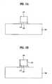
- FIG. 1is a cross sectional view of a conventional thin film transistor.
- a gate oxide film 110is formed on a semiconductor substrate 100 .
- the top surface of the gate oxide film 110is nitridized to form a first nitride layer 120 .
- a polysilicon layer 130is formed on the first nitride layer 120 .
- a pocket 140is formed in a portion of the semiconductor substrate 100 below the edge of the gate oxide film 110 by implanting impurity ions, e.g., boron ions, using a tilt implantation method.
- impurity ionse.g., boron ions
- LDDlightly doped drain
- a spacer which comprises an oxide layer 160 and a second nitride layer 170is formed on the sidewalls of the gate oxide film 110 , first nitride layer, and polysilicon layer 130 . Then, using the spacer 160 and 170 and the polysilicon layer 130 as a mask, impurity ions are implanted at a high density onto the semiconductor substrate 100 to form source/drain regions 180 .
- the first nitride layer 120is formed to prevent ion penetration from the polysilicon layer 130 to the gate oxide film 110 .
- ion penetration from the polysilicon layer 130 to the gate oxide film 110may be prevented, a other problems still remain, for example, ion penetration from the pocket 140 , including the source/drain regions, to the gate oxide film 110 , and electrical stress occurring to the gate oxide film 110 .
- the present inventionis directed to a thin film transistor and method for manufacturing the same, which substantially obviates one or more problems that may be due to limitations and disadvantages of the related art.
- the present inventioncan provide a thin film transistor and method for manufacturing the same in which ion penetration from extended source/drain regions to a gate oxide film and electrical stress occurring to a gate electrode are suppressed, thereby reducing gate leakage and providing a highly reliable transistor.
- a method for manufacturing a thin film transistorthat comprises the steps of forming a gate oxide film on a substrate; forming a first nitride layer on the gate oxide film; forming a polysilicon layer on the first nitride layer; forming a second nitride layer on sidewalls of the gate oxide film, first nitride layer, and polysilicon layer; and implanting impurity ions to form a pocket below the second nitride layer.
- a thin film transistorcomprising a semiconductor substrate; a gate oxide film on the semiconductor substrate; a first nitride layer on the gate oxide film; a polysilicon layer on the first nitride layer; a second nitride layer on sidewalls of the gate oxide film, first nitride layer, and polysilicon layer; and a pocket formed by implanting impurity ions in a portion of the semiconductor substrate below the second nitride layer.
- FIG. 1is a cross sectional view of a conventional thin film transistor
- FIGS. 2A to 2 Eare cross sectional views illustrating a method for manufacturing a thin film transistor according to the present invention.
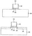
- a gate oxide film 210is formed on a semiconductor substrate 200 , for example, by using a thermal oxidation process.
- the thermal oxidation processcan be performed at a temperature of 650° C. to 750° C. by rapid thermal processing (RTP).
- RTPrapid thermal processing
- the gate oxide film 210has an exemplary thickness of 100 ⁇ to 300 ⁇ .
- the gate oxide film 210is then treated with plasma of a high concentration so that a first nitride layer 220 is formed on the top surface of the gate oxide film 210 .
- the first nitride layer 220has an exemplary thickness of 500 ⁇ to 2000 ⁇ .
- a polysilicon layer 230is formed on the first nitride layer 220 with a low pressure chemical vapor deposition (LPCVD) process.
- LPCVDlow pressure chemical vapor deposition
- a plasma treatmentis performed to form a second nitride layer 240 on sidewalls of the gate oxide film 210 , first nitride layer 220 , and polysilicon layer 230 .
- the edge portion of the gate oxide film 210can be nitridized such that a portion of the second nitride layer 240 is below the first nitride layer 220 .
- the second nitride layercan prevent ion penetration into the gate oxide film 210 from a pocket to be formed later.
- ion implantation for a pocket 250 and ion implantation for a lightly doped drain (LDD) 260are sequentially performed on the semiconductor substrate 200 .
- the implantation for the pocket 250can optionally be performed with a tilt implantation method such that the pocket 250 is formed in a portion of the semiconductor substrate 200 immediately below the second nitride layer 240 , thereby facilitating formation of an extended source/drain region.
- an oxide layer 270for example, a tetra-ethoxysilane (TEOS) oxide layer, is then formed on the sidewall of the second nitride layer 240 by a LPCVD process.
- a first buffer layer 280is formed on the sidewall of the oxide layer 270 .
- the first buffer layer 280serves to suppress electrical stresses occurring on the gate oxide film 210 .
- the first buffer layer 280can be formed with an oxide compound.
- a third nitride layer 290is formed on the sidewall of the first buffer layer 280 .
- a second buffer layer 300is then formed on the sidewall of the third nitride layer 290 .
- the second buffer layer 300can be formed more thickly than the first buffer layer 280 .
- the second buffer layer 290can alleviate stress applied to the polysilicon layer 230 and improve the reliability of the device.
- the third nitride layer 290 and second buffer layer 300constitute a spacer together with the oxide layer 270 and first buffer layer 280 .
- ion implantation for a source/drain region 310is performed on the semiconductor substrate 200 using the polysilicon layer 230 and the spacer as a mask.
- ion penetrationfor example, boron penetration
- boron penetrationfrom extended source/drain regions to a gate oxide film
- a spacer formed on a sidewall of the gate electrodecomprises one or more buffer layers, electrical stresses occurring to the gate electrode can be remarkably mitigated.
- gate leakageis reduced and high reliability of a device is improved.
Landscapes
- Engineering & Computer Science (AREA)
- Physics & Mathematics (AREA)
- Manufacturing & Machinery (AREA)
- Computer Hardware Design (AREA)
- Crystallography & Structural Chemistry (AREA)
- Power Engineering (AREA)
- Condensed Matter Physics & Semiconductors (AREA)
- General Physics & Mathematics (AREA)
- Chemical & Material Sciences (AREA)
- Microelectronics & Electronic Packaging (AREA)
- General Chemical & Material Sciences (AREA)
- Chemical Kinetics & Catalysis (AREA)
- High Energy & Nuclear Physics (AREA)
- Health & Medical Sciences (AREA)
- Toxicology (AREA)
- Insulated Gate Type Field-Effect Transistor (AREA)
- Formation Of Insulating Films (AREA)
Abstract
Description
- This application claims the benefit of Korean Patent Application No. P2004-0106056, filed on Dec. 15, 2004, which is hereby incorporated by reference for all purposes as if fully set forth herein.
- 1. Field of the Invention
- The present invention relates to a thin film transistor and method for manufacturing the same, and more particularly, to a thin film transistor and method for manufacturing the same in which ion penetration from source and drain regions is suppressed, and stress generated from gate sidewalls and an interlayer dielectric film is suppressed.
- 2. Discussion of the Related Art
- The reliability of a complementary metal oxide semiconductor (CMOS) device having high performance and high density is important. If the size of the device is reduced, the thickness of a gate oxide film is correspondingly thinned. However, a power source supplied through a power supplier is not decreased in proportion to the thickness reduction. Accordingly, electrical stress is generated that reduces the reliability of the gate oxide film.
FIG. 1 is a cross sectional view of a conventional thin film transistor.- Referring to
FIG. 1 , agate oxide film 110 is formed on asemiconductor substrate 100. The top surface of thegate oxide film 110 is nitridized to form afirst nitride layer 120. On thefirst nitride layer 120, apolysilicon layer 130 is formed. Apocket 140 is formed in a portion of thesemiconductor substrate 100 below the edge of thegate oxide film 110 by implanting impurity ions, e.g., boron ions, using a tilt implantation method. Subsequently, a lightly doped drain (LDD) is formed in thesemiconductor substrate 100 by implanting impurity ions onto thesemiconductor substrate 100 using thepolysilicon layer 130 as a mask. A spacer which comprises anoxide layer 160 and asecond nitride layer 170 is formed on the sidewalls of thegate oxide film 110, first nitride layer, andpolysilicon layer 130. Then, using thespacer polysilicon layer 130 as a mask, impurity ions are implanted at a high density onto thesemiconductor substrate 100 to form source/drain regions 180. - The
first nitride layer 120 is formed to prevent ion penetration from thepolysilicon layer 130 to thegate oxide film 110. - Although ion penetration from the
polysilicon layer 130 to thegate oxide film 110 may be prevented, a other problems still remain, for example, ion penetration from thepocket 140, including the source/drain regions, to thegate oxide film 110, and electrical stress occurring to thegate oxide film 110. - Accordingly, the present invention is directed to a thin film transistor and method for manufacturing the same, which substantially obviates one or more problems that may be due to limitations and disadvantages of the related art.
- The present invention can provide a thin film transistor and method for manufacturing the same in which ion penetration from extended source/drain regions to a gate oxide film and electrical stress occurring to a gate electrode are suppressed, thereby reducing gate leakage and providing a highly reliable transistor.
- Additional advantages and features of the invention will be set forth in part in the description which follows and in part will become apparent to those having ordinary skill in the art upon examination of the following. These and other advantages of the invention may be realized and attained by the structure particularly pointed out in the written description and claims hereof as well as the appended drawings.
- To achieve these and other advantages and in accordance with the invention, as embodied and broadly described herein, there is provided a method for manufacturing a thin film transistor that comprises the steps of forming a gate oxide film on a substrate; forming a first nitride layer on the gate oxide film; forming a polysilicon layer on the first nitride layer; forming a second nitride layer on sidewalls of the gate oxide film, first nitride layer, and polysilicon layer; and implanting impurity ions to form a pocket below the second nitride layer.
- In another aspect of the present invention, there is provided a thin film transistor comprising a semiconductor substrate; a gate oxide film on the semiconductor substrate; a first nitride layer on the gate oxide film; a polysilicon layer on the first nitride layer; a second nitride layer on sidewalls of the gate oxide film, first nitride layer, and polysilicon layer; and a pocket formed by implanting impurity ions in a portion of the semiconductor substrate below the second nitride layer.
- It is to be understood that both the foregoing general description and the following detailed description of the present invention are exemplary and explanatory and are intended to provide further explanation of the invention as claimed.
- The accompanying drawings, which are included to provide a further understanding of the invention illustrate embodiments of the invention and together with the description serve to explain the principle of the invention. In the drawings:
FIG. 1 is a cross sectional view of a conventional thin film transistor; andFIGS. 2A to2E are cross sectional views illustrating a method for manufacturing a thin film transistor according to the present invention.- Reference will now be made in detail to embodiments of the present invention, examples of which are illustrated in the accompanying drawings. Wherever possible, the same reference numbers will be used throughout the drawings to refer to the same or like parts.
- Referring to
FIG. 2A , agate oxide film 210 is formed on asemiconductor substrate 200, for example, by using a thermal oxidation process. The thermal oxidation process can be performed at a temperature of 650° C. to 750° C. by rapid thermal processing (RTP). Thegate oxide film 210 has an exemplary thickness of 100 Å to 300 Å. - The
gate oxide film 210 is then treated with plasma of a high concentration so that afirst nitride layer 220 is formed on the top surface of thegate oxide film 210. Thefirst nitride layer 220 has an exemplary thickness of 500 Å to 2000 Å. - Subsequently, a
polysilicon layer 230 is formed on thefirst nitride layer 220 with a low pressure chemical vapor deposition (LPCVD) process. - Then, as shown in
FIG. 2B , a plasma treatment is performed to form asecond nitride layer 240 on sidewalls of thegate oxide film 210,first nitride layer 220, andpolysilicon layer 230. The edge portion of thegate oxide film 210 can be nitridized such that a portion of thesecond nitride layer 240 is below thefirst nitride layer 220. - The second nitride layer can prevent ion penetration into the
gate oxide film 210 from a pocket to be formed later. - Referring to
FIG. 2C , ion implantation for apocket 250 and ion implantation for a lightly doped drain (LDD)260 are sequentially performed on thesemiconductor substrate 200. The implantation for thepocket 250 can optionally be performed with a tilt implantation method such that thepocket 250 is formed in a portion of thesemiconductor substrate 200 immediately below thesecond nitride layer 240, thereby facilitating formation of an extended source/drain region. - Referring to
FIG. 2D , anoxide layer 270, for example, a tetra-ethoxysilane (TEOS) oxide layer, is then formed on the sidewall of thesecond nitride layer 240 by a LPCVD process. After theoxide layer 270 is deposited, afirst buffer layer 280 is formed on the sidewall of theoxide layer 270. Thefirst buffer layer 280 serves to suppress electrical stresses occurring on thegate oxide film 210. Thefirst buffer layer 280 can be formed with an oxide compound. - Referring to
FIG. 2E , athird nitride layer 290 is formed on the sidewall of thefirst buffer layer 280. Asecond buffer layer 300 is then formed on the sidewall of thethird nitride layer 290. Thesecond buffer layer 300 can be formed more thickly than thefirst buffer layer 280. Thesecond buffer layer 290 can alleviate stress applied to thepolysilicon layer 230 and improve the reliability of the device. - The
third nitride layer 290 andsecond buffer layer 300 constitute a spacer together with theoxide layer 270 andfirst buffer layer 280. - Subsequently, ion implantation for a source/
drain region 310 is performed on thesemiconductor substrate 200 using thepolysilicon layer 230 and the spacer as a mask. - By performing plasma treatment on a gate electrode, and thus forming nitride layer on the sidewall thereof, ion penetration, for example, boron penetration, from extended source/drain regions to a gate oxide film may be highly suppressed. Furthermore, since a spacer formed on a sidewall of the gate electrode comprises one or more buffer layers, electrical stresses occurring to the gate electrode can be remarkably mitigated. Thus, gate leakage is reduced and high reliability of a device is improved.
- It will be apparent to those skilled in the art that various modifications and variations can be made in the present invention without departing from the spirit or scope of the inventions. Thus, it is intended that the present invention covers the modifications and variations of this invention provided they come within the scope of the appended claims and their equivalents.
Claims (20)
Applications Claiming Priority (2)
| Application Number | Priority Date | Filing Date | Title |
|---|---|---|---|
| KR1020040106056AKR100668954B1 (en) | 2004-12-15 | 2004-12-15 | Method of manufacturing thin film transistor |
| KR2004-0106056 | 2004-12-15 |
Publications (2)
| Publication Number | Publication Date |
|---|---|
| US20060128077A1true US20060128077A1 (en) | 2006-06-15 |
| US7507611B2 US7507611B2 (en) | 2009-03-24 |
Family
ID=36584511
Family Applications (1)
| Application Number | Title | Priority Date | Filing Date |
|---|---|---|---|
| US11/300,439Expired - Fee RelatedUS7507611B2 (en) | 2004-12-15 | 2005-12-15 | Thin film transistor and method for manufacturing the same |
Country Status (2)
| Country | Link |
|---|---|
| US (1) | US7507611B2 (en) |
| KR (1) | KR100668954B1 (en) |
Cited By (2)
| Publication number | Priority date | Publication date | Assignee | Title |
|---|---|---|---|---|
| US20180013095A1 (en)* | 2016-07-05 | 2018-01-11 | Samsung Display Co., Ltd. | Display device |
| US10243060B2 (en)* | 2017-03-24 | 2019-03-26 | International Business Machines Corporation | Uniform low-k inner spacer module in gate-all-around (GAA) transistors |
Families Citing this family (4)
| Publication number | Priority date | Publication date | Assignee | Title |
|---|---|---|---|---|
| US6660657B1 (en)* | 2000-08-07 | 2003-12-09 | Micron Technology, Inc. | Methods of incorporating nitrogen into silicon-oxide-containing layers |
| KR100846097B1 (en) | 2007-06-29 | 2008-07-14 | 삼성전자주식회사 | Manufacturing Method of Semiconductor Device |
| JP6510289B2 (en)* | 2015-03-30 | 2019-05-08 | ルネサスエレクトロニクス株式会社 | Semiconductor device and method of manufacturing the same |
| US9876069B1 (en)* | 2017-05-18 | 2018-01-23 | Vanguard International Semiconductor Corporation | High-voltage semiconductor device and method for manufacturing the same |
Citations (49)
| Publication number | Priority date | Publication date | Assignee | Title |
|---|---|---|---|---|
| US5324974A (en)* | 1990-09-04 | 1994-06-28 | Industrial Technology Research Institute | Nitride capped MOSFET for integrated circuits |
| US5414287A (en)* | 1994-04-25 | 1995-05-09 | United Microelectronics Corporation | Process for high density split-gate memory cell for flash or EPROM |
| US5837598A (en)* | 1997-03-13 | 1998-11-17 | Lsi Logic Corporation | Diffusion barrier for polysilicon gate electrode of MOS device in integrated circuit structure, and method of making same |
| US5847428A (en)* | 1996-12-06 | 1998-12-08 | Advanced Micro Devices, Inc. | Integrated circuit gate conductor which uses layered spacers to produce a graded junction |
| US5969397A (en)* | 1996-11-26 | 1999-10-19 | Texas Instruments Incorporated | Low defect density composite dielectric |
| US5986312A (en)* | 1995-02-07 | 1999-11-16 | Sony Corporation | Field effect semiconductor device having improved connections |
| US6051865A (en)* | 1998-11-09 | 2000-04-18 | Advanced Micro Devices, Inc. | Transistor having a barrier layer below a high permittivity gate dielectric |
| US6087229A (en)* | 1998-03-09 | 2000-07-11 | Lsi Logic Corporation | Composite semiconductor gate dielectrics |
| US6093661A (en)* | 1999-08-30 | 2000-07-25 | Micron Technology, Inc. | Integrated circuitry and semiconductor processing method of forming field effect transistors |
| US6188115B1 (en)* | 1998-01-30 | 2001-02-13 | Mitsubishi Denki Kabushiki Kaisha | Semiconductor device with a conductive layer of small conductive resistance |
| US6245625B1 (en)* | 1999-06-19 | 2001-06-12 | United Microelectronics Corp. | Fabrication method of a self-aligned contact window |
| US6316321B1 (en)* | 1999-05-19 | 2001-11-13 | United Microelectronics Corp. | Method for forming MOSFET |
| US6331468B1 (en)* | 1998-05-11 | 2001-12-18 | Lsi Logic Corporation | Formation of integrated circuit structure using one or more silicon layers for implantation and out-diffusion in formation of defect-free source/drain regions and also for subsequent formation of silicon nitride spacers |
| US20020052124A1 (en)* | 1999-12-23 | 2002-05-02 | Ivo Raaijmakers | In situ dielectric stacks |
| US6417085B1 (en)* | 1999-07-02 | 2002-07-09 | Micron Technology, Inc. | Methods of forming a field effect transistor gate construction |
| US20020109197A1 (en)* | 2000-09-28 | 2002-08-15 | Ryoichi Nakamura | Semiconductor device and method for its manufacture |
| US6455389B1 (en)* | 2001-06-01 | 2002-09-24 | Kuo-Tai Huang | Method for preventing a by-product ion moving from a spacer |
| US20020163039A1 (en)* | 2001-05-04 | 2002-11-07 | Clevenger Lawrence A. | High dielectric constant materials as gate dielectrics (insulators) |
| US6509611B1 (en)* | 2001-09-21 | 2003-01-21 | International Business Machines Corporation | Method for wrapped-gate MOSFET |
| US6512273B1 (en)* | 2000-01-28 | 2003-01-28 | Advanced Micro Devices, Inc. | Method and structure for improving hot carrier immunity for devices with very shallow junctions |
| US6555438B1 (en)* | 1998-02-19 | 2003-04-29 | Shye-Lin Wu | Method for fabricating MOSFETs with a recessed self-aligned silicide contact and extended source/drain junctions |
| US6607990B2 (en)* | 1999-09-24 | 2003-08-19 | Kabushiki Kaisha Toshiba | Semiconductor device and its manufacturing method |
| US6610571B1 (en)* | 2002-02-07 | 2003-08-26 | Taiwan Semiconductor Manufacturing Company | Approach to prevent spacer undercut by low temperature nitridation |
| US20030203556A1 (en)* | 2000-09-18 | 2003-10-30 | Matsushita Electric Industrial Co., Ltd. | Semiconductor device and method for facticating the same |
| US6649543B1 (en)* | 2000-06-22 | 2003-11-18 | Micron Technology, Inc. | Methods of forming silicon nitride, methods of forming transistor devices, and transistor devices |
| US6660658B2 (en)* | 2000-08-07 | 2003-12-09 | Micron Technology, Inc. | Transistor structures, methods of incorporating nitrogen into silicon-oxide-containing layers; and methods of forming transistors |
| US6686298B1 (en)* | 2000-06-22 | 2004-02-03 | Micron Technology, Inc. | Methods of forming structures over semiconductor substrates, and methods of forming transistors associated with semiconductor substrates |
| US20040171261A1 (en)* | 2003-02-28 | 2004-09-02 | Jong-Heui Song | Method of etching a silicon nitride film and method of manufacturing a semiconductor device using the same |
| US6803624B2 (en)* | 2002-07-03 | 2004-10-12 | Micron Technology, Inc. | Programmable memory devices supported by semiconductive substrates |
| US6806517B2 (en)* | 2003-03-17 | 2004-10-19 | Samsung Electronics Co., Ltd. | Flash memory having local SONOS structure using notched gate and manufacturing method thereof |
| US20040245564A1 (en)* | 2003-05-19 | 2004-12-09 | Takayuki Ogura | Semiconductor storage device, semiconductor device and their manufacturing methods, and portable electronic equipment, and IC card |
| US6833329B1 (en)* | 2000-06-22 | 2004-12-21 | Micron Technology, Inc. | Methods of forming oxide regions over semiconductor substrates |
| US20040266154A1 (en)* | 2003-06-30 | 2004-12-30 | Hynix Semiconductor Inc. | Method for fabricating transistor with polymetal gate electrode |
| US6846716B2 (en)* | 2002-03-19 | 2005-01-25 | Freescale Semiconductor, Inc. | Integrated circuit device and method therefor |
| US20050048732A1 (en)* | 2003-08-26 | 2005-03-03 | International Business Machines Corporation | Method to produce transistor having reduced gate height |
| US20050059228A1 (en)* | 2003-09-15 | 2005-03-17 | Haowen Bu | Integration of pre-S/D anneal selective nitride/oxide composite cap for improving transistor performance |
| US20050064690A1 (en)* | 2003-09-18 | 2005-03-24 | International Business Machines Corporation | Process options of forming silicided metal gates for advanced cmos devices |
| US20050136606A1 (en)* | 2003-12-19 | 2005-06-23 | Hartmut Rulke | Spacer for a gate electrode having tensile stress and a method of forming the same |
| US20050156229A1 (en)* | 2003-12-16 | 2005-07-21 | Yeap Geoffrey C. | Integrated circuit device and method therefor |
| US20050189660A1 (en)* | 2002-12-10 | 2005-09-01 | Haowen Bu | Source drain and extension dopant concentration |
| US20050250287A1 (en)* | 2004-05-05 | 2005-11-10 | Jian Chen | Method of semiconductor fabrication incorporating disposable spacer into elevated source/drain processing |
| US20050275046A1 (en)* | 2004-06-14 | 2005-12-15 | Matthias Goldbach | Multi-layer gate stack structure comprising a metal layer for a fet device, and method for fabricating the same |
| US20050280123A1 (en)* | 2004-06-22 | 2005-12-22 | Jae-Suk Lee | Semiconductor devices and methods of manufacturing the same |
| US6995066B2 (en)* | 2003-12-31 | 2006-02-07 | Dongbuanam Semiconductor Inc. | Method of fabricating semiconductor device by using sacrifice layer for forming diffusion regions |
| US7161203B2 (en)* | 2004-06-04 | 2007-01-09 | Micron Technology, Inc. | Gated field effect device comprising gate dielectric having different K regions |
| US7192881B2 (en)* | 2003-11-28 | 2007-03-20 | Advanced Micro Devices, Inc. | Method of forming sidewall spacer elements for a circuit element by increasing an etch selectivity |
| US7217624B2 (en)* | 2004-10-01 | 2007-05-15 | Hynix Semiconductor Inc. | Non-volatile memory device with conductive sidewall spacer and method for fabricating the same |
| US7220651B2 (en)* | 2004-03-11 | 2007-05-22 | Hynix Semiconductor, Inc | Transistor and method for manufacturing the same |
| US7419879B2 (en)* | 2005-01-12 | 2008-09-02 | Samsung Electronics Co., Ltd. | Transistor having gate dielectric layer of partial thickness difference and method of fabricating the same |
- 2004
- 2004-12-15KRKR1020040106056Apatent/KR100668954B1/ennot_activeExpired - Fee Related
- 2005
- 2005-12-15USUS11/300,439patent/US7507611B2/ennot_activeExpired - Fee Related
Patent Citations (55)
| Publication number | Priority date | Publication date | Assignee | Title |
|---|---|---|---|---|
| US5324974A (en)* | 1990-09-04 | 1994-06-28 | Industrial Technology Research Institute | Nitride capped MOSFET for integrated circuits |
| US5414287A (en)* | 1994-04-25 | 1995-05-09 | United Microelectronics Corporation | Process for high density split-gate memory cell for flash or EPROM |
| US5986312A (en)* | 1995-02-07 | 1999-11-16 | Sony Corporation | Field effect semiconductor device having improved connections |
| US5969397A (en)* | 1996-11-26 | 1999-10-19 | Texas Instruments Incorporated | Low defect density composite dielectric |
| US5847428A (en)* | 1996-12-06 | 1998-12-08 | Advanced Micro Devices, Inc. | Integrated circuit gate conductor which uses layered spacers to produce a graded junction |
| US5837598A (en)* | 1997-03-13 | 1998-11-17 | Lsi Logic Corporation | Diffusion barrier for polysilicon gate electrode of MOS device in integrated circuit structure, and method of making same |
| US6188115B1 (en)* | 1998-01-30 | 2001-02-13 | Mitsubishi Denki Kabushiki Kaisha | Semiconductor device with a conductive layer of small conductive resistance |
| US6555438B1 (en)* | 1998-02-19 | 2003-04-29 | Shye-Lin Wu | Method for fabricating MOSFETs with a recessed self-aligned silicide contact and extended source/drain junctions |
| US6087229A (en)* | 1998-03-09 | 2000-07-11 | Lsi Logic Corporation | Composite semiconductor gate dielectrics |
| US6331468B1 (en)* | 1998-05-11 | 2001-12-18 | Lsi Logic Corporation | Formation of integrated circuit structure using one or more silicon layers for implantation and out-diffusion in formation of defect-free source/drain regions and also for subsequent formation of silicon nitride spacers |
| US6051865A (en)* | 1998-11-09 | 2000-04-18 | Advanced Micro Devices, Inc. | Transistor having a barrier layer below a high permittivity gate dielectric |
| US6316321B1 (en)* | 1999-05-19 | 2001-11-13 | United Microelectronics Corp. | Method for forming MOSFET |
| US6245625B1 (en)* | 1999-06-19 | 2001-06-12 | United Microelectronics Corp. | Fabrication method of a self-aligned contact window |
| US6417085B1 (en)* | 1999-07-02 | 2002-07-09 | Micron Technology, Inc. | Methods of forming a field effect transistor gate construction |
| US6093661A (en)* | 1999-08-30 | 2000-07-25 | Micron Technology, Inc. | Integrated circuitry and semiconductor processing method of forming field effect transistors |
| US6607990B2 (en)* | 1999-09-24 | 2003-08-19 | Kabushiki Kaisha Toshiba | Semiconductor device and its manufacturing method |
| US20020052124A1 (en)* | 1999-12-23 | 2002-05-02 | Ivo Raaijmakers | In situ dielectric stacks |
| US6512273B1 (en)* | 2000-01-28 | 2003-01-28 | Advanced Micro Devices, Inc. | Method and structure for improving hot carrier immunity for devices with very shallow junctions |
| US6833329B1 (en)* | 2000-06-22 | 2004-12-21 | Micron Technology, Inc. | Methods of forming oxide regions over semiconductor substrates |
| US6815375B2 (en)* | 2000-06-22 | 2004-11-09 | Micron Technology, Inc. | Methods of forming dielectric materials and methods of processing semiconductor substrates |
| US6744098B2 (en)* | 2000-06-22 | 2004-06-01 | Micron Technology, Inc. | Transistor devices |
| US6690046B2 (en)* | 2000-06-22 | 2004-02-10 | Micron Technology, Inc. | Semiconductor assemblies, methods of forming structures over semiconductor substrates, and methods of forming transistors associated with semiconductor substrates |
| US6686298B1 (en)* | 2000-06-22 | 2004-02-03 | Micron Technology, Inc. | Methods of forming structures over semiconductor substrates, and methods of forming transistors associated with semiconductor substrates |
| US6649543B1 (en)* | 2000-06-22 | 2003-11-18 | Micron Technology, Inc. | Methods of forming silicon nitride, methods of forming transistor devices, and transistor devices |
| US6660658B2 (en)* | 2000-08-07 | 2003-12-09 | Micron Technology, Inc. | Transistor structures, methods of incorporating nitrogen into silicon-oxide-containing layers; and methods of forming transistors |
| US6660657B1 (en)* | 2000-08-07 | 2003-12-09 | Micron Technology, Inc. | Methods of incorporating nitrogen into silicon-oxide-containing layers |
| US7344948B2 (en)* | 2000-08-07 | 2008-03-18 | Micron Technology, Inc. | Methods of forming transistors |
| US20030203556A1 (en)* | 2000-09-18 | 2003-10-30 | Matsushita Electric Industrial Co., Ltd. | Semiconductor device and method for facticating the same |
| US20020109197A1 (en)* | 2000-09-28 | 2002-08-15 | Ryoichi Nakamura | Semiconductor device and method for its manufacture |
| US20020163039A1 (en)* | 2001-05-04 | 2002-11-07 | Clevenger Lawrence A. | High dielectric constant materials as gate dielectrics (insulators) |
| US6455389B1 (en)* | 2001-06-01 | 2002-09-24 | Kuo-Tai Huang | Method for preventing a by-product ion moving from a spacer |
| US6509611B1 (en)* | 2001-09-21 | 2003-01-21 | International Business Machines Corporation | Method for wrapped-gate MOSFET |
| US6610571B1 (en)* | 2002-02-07 | 2003-08-26 | Taiwan Semiconductor Manufacturing Company | Approach to prevent spacer undercut by low temperature nitridation |
| US6846716B2 (en)* | 2002-03-19 | 2005-01-25 | Freescale Semiconductor, Inc. | Integrated circuit device and method therefor |
| US6803624B2 (en)* | 2002-07-03 | 2004-10-12 | Micron Technology, Inc. | Programmable memory devices supported by semiconductive substrates |
| US20050189660A1 (en)* | 2002-12-10 | 2005-09-01 | Haowen Bu | Source drain and extension dopant concentration |
| US20040171261A1 (en)* | 2003-02-28 | 2004-09-02 | Jong-Heui Song | Method of etching a silicon nitride film and method of manufacturing a semiconductor device using the same |
| US6806517B2 (en)* | 2003-03-17 | 2004-10-19 | Samsung Electronics Co., Ltd. | Flash memory having local SONOS structure using notched gate and manufacturing method thereof |
| US20040245564A1 (en)* | 2003-05-19 | 2004-12-09 | Takayuki Ogura | Semiconductor storage device, semiconductor device and their manufacturing methods, and portable electronic equipment, and IC card |
| US20040266154A1 (en)* | 2003-06-30 | 2004-12-30 | Hynix Semiconductor Inc. | Method for fabricating transistor with polymetal gate electrode |
| US20050048732A1 (en)* | 2003-08-26 | 2005-03-03 | International Business Machines Corporation | Method to produce transistor having reduced gate height |
| US20050059228A1 (en)* | 2003-09-15 | 2005-03-17 | Haowen Bu | Integration of pre-S/D anneal selective nitride/oxide composite cap for improving transistor performance |
| US20050164431A1 (en)* | 2003-09-15 | 2005-07-28 | Haowen Bu | Integration of pre-S/D anneal selective nitride/oxide composite cap for improving transistor performance |
| US20050064690A1 (en)* | 2003-09-18 | 2005-03-24 | International Business Machines Corporation | Process options of forming silicided metal gates for advanced cmos devices |
| US7192881B2 (en)* | 2003-11-28 | 2007-03-20 | Advanced Micro Devices, Inc. | Method of forming sidewall spacer elements for a circuit element by increasing an etch selectivity |
| US20050156229A1 (en)* | 2003-12-16 | 2005-07-21 | Yeap Geoffrey C. | Integrated circuit device and method therefor |
| US20050136606A1 (en)* | 2003-12-19 | 2005-06-23 | Hartmut Rulke | Spacer for a gate electrode having tensile stress and a method of forming the same |
| US6995066B2 (en)* | 2003-12-31 | 2006-02-07 | Dongbuanam Semiconductor Inc. | Method of fabricating semiconductor device by using sacrifice layer for forming diffusion regions |
| US7220651B2 (en)* | 2004-03-11 | 2007-05-22 | Hynix Semiconductor, Inc | Transistor and method for manufacturing the same |
| US20050250287A1 (en)* | 2004-05-05 | 2005-11-10 | Jian Chen | Method of semiconductor fabrication incorporating disposable spacer into elevated source/drain processing |
| US7161203B2 (en)* | 2004-06-04 | 2007-01-09 | Micron Technology, Inc. | Gated field effect device comprising gate dielectric having different K regions |
| US20050275046A1 (en)* | 2004-06-14 | 2005-12-15 | Matthias Goldbach | Multi-layer gate stack structure comprising a metal layer for a fet device, and method for fabricating the same |
| US20050280123A1 (en)* | 2004-06-22 | 2005-12-22 | Jae-Suk Lee | Semiconductor devices and methods of manufacturing the same |
| US7217624B2 (en)* | 2004-10-01 | 2007-05-15 | Hynix Semiconductor Inc. | Non-volatile memory device with conductive sidewall spacer and method for fabricating the same |
| US7419879B2 (en)* | 2005-01-12 | 2008-09-02 | Samsung Electronics Co., Ltd. | Transistor having gate dielectric layer of partial thickness difference and method of fabricating the same |
Cited By (3)
| Publication number | Priority date | Publication date | Assignee | Title |
|---|---|---|---|---|
| US20180013095A1 (en)* | 2016-07-05 | 2018-01-11 | Samsung Display Co., Ltd. | Display device |
| US10547025B2 (en)* | 2016-07-05 | 2020-01-28 | Samsung Display Co., Ltd. | Display device |
| US10243060B2 (en)* | 2017-03-24 | 2019-03-26 | International Business Machines Corporation | Uniform low-k inner spacer module in gate-all-around (GAA) transistors |
Also Published As
| Publication number | Publication date |
|---|---|
| KR20060068104A (en) | 2006-06-21 |
| US7507611B2 (en) | 2009-03-24 |
| KR100668954B1 (en) | 2007-01-12 |
Similar Documents
| Publication | Publication Date | Title |
|---|---|---|
| US6902971B2 (en) | Transistor sidewall spacer stress modulation | |
| US20040033677A1 (en) | Method and apparatus to prevent lateral oxidation in a transistor utilizing an ultra thin oxygen-diffusion barrier | |
| US20030082863A1 (en) | CMOS of semiconductor device and method for manufacturing the same | |
| US20070200185A1 (en) | Semiconductor device and method for fabricating the same | |
| US7611949B2 (en) | Method of fabricating metal-oxide-semiconductor transistor | |
| US20080272420A1 (en) | CMOS image sensor and manufacturing method thereof | |
| WO2011036841A1 (en) | Semiconductor device and method for manufacturing same | |
| US12125909B2 (en) | Asymmetric semiconductor device including LDD region and manufacturing method thereof | |
| US7507611B2 (en) | Thin film transistor and method for manufacturing the same | |
| US20080308895A1 (en) | Semiconductor device | |
| US7892935B2 (en) | Semiconductor process | |
| US7863692B2 (en) | Semiconductor device | |
| US20050048754A1 (en) | Processing method for increasing packaging density of an integrated circuit | |
| US20010044191A1 (en) | Method for manufacturing semiconductor device | |
| US20060154425A1 (en) | Semiconductor device and method for fabricating the same | |
| US20050260817A1 (en) | Semiconductor device and method for manufacturing the same | |
| US7361580B2 (en) | Semiconductor device and manufacturing method thereof | |
| US20090159994A1 (en) | Semiconductor device and method of manufacturing the same | |
| US20080237744A1 (en) | Semiconductor Device and Manufacturing Method Thereof | |
| US7157343B2 (en) | Method for fabricating semiconductor device | |
| TWI402920B (en) | Semiconductor device and method of manufacturing thereof | |
| US7332796B2 (en) | Devices and methods of preventing plasma charging damage in semiconductor devices | |
| US7126189B2 (en) | Method for fabricating semiconductor device | |
| US20080157233A1 (en) | Method for fabricating a semiconductor device | |
| US7371655B2 (en) | Method of fabricating low-power CMOS device |
Legal Events
| Date | Code | Title | Description |
|---|---|---|---|
| AS | Assignment | Owner name:DONGBU-ANAM SEMICONDUCTOR, KOREA, REPUBLIC OF Free format text:ASSIGNMENT OF ASSIGNORS INTEREST;ASSIGNOR:PARK, HYUK;REEL/FRAME:017369/0496 Effective date:20051214 | |
| AS | Assignment | Owner name:DONGBU ELECTRONICS CO., LTD.,KOREA, REPUBLIC OF Free format text:CHANGE OF NAME;ASSIGNOR:DONGBUANAM SEMICONDUCTOR INC.;REEL/FRAME:018176/0351 Effective date:20060324 Owner name:DONGBU ELECTRONICS CO., LTD., KOREA, REPUBLIC OF Free format text:CHANGE OF NAME;ASSIGNOR:DONGBUANAM SEMICONDUCTOR INC.;REEL/FRAME:018176/0351 Effective date:20060324 | |
| FEPP | Fee payment procedure | Free format text:PAYOR NUMBER ASSIGNED (ORIGINAL EVENT CODE: ASPN); ENTITY STATUS OF PATENT OWNER: LARGE ENTITY | |
| FEPP | Fee payment procedure | Free format text:PAYER NUMBER DE-ASSIGNED (ORIGINAL EVENT CODE: RMPN); ENTITY STATUS OF PATENT OWNER: LARGE ENTITY Free format text:PAYOR NUMBER ASSIGNED (ORIGINAL EVENT CODE: ASPN); ENTITY STATUS OF PATENT OWNER: LARGE ENTITY | |
| FPAY | Fee payment | Year of fee payment:4 | |
| REMI | Maintenance fee reminder mailed | ||
| LAPS | Lapse for failure to pay maintenance fees | ||
| STCH | Information on status: patent discontinuation | Free format text:PATENT EXPIRED DUE TO NONPAYMENT OF MAINTENANCE FEES UNDER 37 CFR 1.362 | |
| FP | Lapsed due to failure to pay maintenance fee | Effective date:20170324 |