US20060126374A1 - Sense amplifier circuitry and architecture to write data into and/or read from memory cells - Google Patents
Sense amplifier circuitry and architecture to write data into and/or read from memory cellsDownload PDFInfo
- Publication number
- US20060126374A1 US20060126374A1US11/299,590US29959005AUS2006126374A1US 20060126374 A1US20060126374 A1US 20060126374A1US 29959005 AUS29959005 AUS 29959005AUS 2006126374 A1US2006126374 A1US 2006126374A1
- Authority
- US
- United States
- Prior art keywords
- transistor
- sense amplifier
- input node
- memory cell
- circuitry
- Prior art date
- Legal status (The legal status is an assumption and is not a legal conclusion. Google has not performed a legal analysis and makes no representation as to the accuracy of the status listed.)
- Granted
Links
- 210000000746body regionAnatomy0.000claimsdescription44
- 238000007599dischargingMethods0.000claimsdescription10
- 238000000034methodMethods0.000abstractdescription58
- 238000005070samplingMethods0.000abstractdescription6
- 230000001066destructive effectEffects0.000abstractdescription4
- 239000000463materialSubstances0.000description25
- 239000004065semiconductorSubstances0.000description20
- 238000005516engineering processMethods0.000description12
- 238000003491arrayMethods0.000description9
- 239000000969carrierSubstances0.000description9
- 230000000295complement effectEffects0.000description8
- 238000012360testing methodMethods0.000description7
- 239000000758substrateSubstances0.000description6
- 238000010586diagramMethods0.000description5
- 238000004519manufacturing processMethods0.000description5
- XUIMIQQOPSSXEZ-UHFFFAOYSA-NSiliconChemical compound[Si]XUIMIQQOPSSXEZ-UHFFFAOYSA-N0.000description3
- 238000007796conventional methodMethods0.000description3
- 239000007943implantSubstances0.000description3
- 238000009413insulationMethods0.000description3
- 230000004044responseEffects0.000description3
- 229910052710siliconInorganic materials0.000description3
- 239000010703siliconSubstances0.000description3
- 229910052732germaniumInorganic materials0.000description2
- GNPVGFCGXDBREM-UHFFFAOYSA-Ngermanium atomChemical compound[Ge]GNPVGFCGXDBREM-UHFFFAOYSA-N0.000description2
- 238000012986modificationMethods0.000description2
- 230000004048modificationEffects0.000description2
- JBRZTFJDHDCESZ-UHFFFAOYSA-NAsGaChemical compound[As]#[Ga]JBRZTFJDHDCESZ-UHFFFAOYSA-N0.000description1
- 229910001218Gallium arsenideInorganic materials0.000description1
- 230000015572biosynthetic processEffects0.000description1
- 239000013590bulk materialSubstances0.000description1
- 239000002800charge carrierSubstances0.000description1
- 230000003247decreasing effectEffects0.000description1
- 238000013461designMethods0.000description1
- 230000000694effectsEffects0.000description1
- 230000007274generation of a signal involved in cell-cell signalingEffects0.000description1
- 238000010348incorporationMethods0.000description1
- 239000012212insulatorSubstances0.000description1
- 230000002093peripheral effectEffects0.000description1
- 230000002123temporal effectEffects0.000description1
Images


Classifications
- G—PHYSICS
- G11—INFORMATION STORAGE
- G11C—STATIC STORES
- G11C11/00—Digital stores characterised by the use of particular electric or magnetic storage elements; Storage elements therefor
- G11C11/21—Digital stores characterised by the use of particular electric or magnetic storage elements; Storage elements therefor using electric elements
- G11C11/34—Digital stores characterised by the use of particular electric or magnetic storage elements; Storage elements therefor using electric elements using semiconductor devices
- G11C11/40—Digital stores characterised by the use of particular electric or magnetic storage elements; Storage elements therefor using electric elements using semiconductor devices using transistors
- G11C11/401—Digital stores characterised by the use of particular electric or magnetic storage elements; Storage elements therefor using electric elements using semiconductor devices using transistors forming cells needing refreshing or charge regeneration, i.e. dynamic cells
- G11C11/4063—Auxiliary circuits, e.g. for addressing, decoding, driving, writing, sensing or timing
- G11C11/407—Auxiliary circuits, e.g. for addressing, decoding, driving, writing, sensing or timing for memory cells of the field-effect type
- G11C11/409—Read-write [R-W] circuits
- G11C11/4091—Sense or sense/refresh amplifiers, or associated sense circuitry, e.g. for coupled bit-line precharging, equalising or isolating
- G—PHYSICS
- G11—INFORMATION STORAGE
- G11C—STATIC STORES
- G11C7/00—Arrangements for writing information into, or reading information out from, a digital store
- G11C7/06—Sense amplifiers; Associated circuits, e.g. timing or triggering circuits
- G11C7/065—Differential amplifiers of latching type
- H—ELECTRICITY
- H10—SEMICONDUCTOR DEVICES; ELECTRIC SOLID-STATE DEVICES NOT OTHERWISE PROVIDED FOR
- H10B—ELECTRONIC MEMORY DEVICES
- H10B12/00—Dynamic random access memory [DRAM] devices
- H—ELECTRICITY
- H10—SEMICONDUCTOR DEVICES; ELECTRIC SOLID-STATE DEVICES NOT OTHERWISE PROVIDED FOR
- H10B—ELECTRONIC MEMORY DEVICES
- H10B12/00—Dynamic random access memory [DRAM] devices
- H10B12/20—DRAM devices comprising floating-body transistors, e.g. floating-body cells
- H—ELECTRICITY
- H10—SEMICONDUCTOR DEVICES; ELECTRIC SOLID-STATE DEVICES NOT OTHERWISE PROVIDED FOR
- H10D—INORGANIC ELECTRIC SEMICONDUCTOR DEVICES
- H10D30/00—Field-effect transistors [FET]
- H10D30/60—Insulated-gate field-effect transistors [IGFET]
- H10D30/711—Insulated-gate field-effect transistors [IGFET] having floating bodies
- G—PHYSICS
- G11—INFORMATION STORAGE
- G11C—STATIC STORES
- G11C11/00—Digital stores characterised by the use of particular electric or magnetic storage elements; Storage elements therefor
- G11C11/21—Digital stores characterised by the use of particular electric or magnetic storage elements; Storage elements therefor using electric elements
- G11C11/34—Digital stores characterised by the use of particular electric or magnetic storage elements; Storage elements therefor using electric elements using semiconductor devices
- G11C11/40—Digital stores characterised by the use of particular electric or magnetic storage elements; Storage elements therefor using electric elements using semiconductor devices using transistors
- G11C11/401—Digital stores characterised by the use of particular electric or magnetic storage elements; Storage elements therefor using electric elements using semiconductor devices using transistors forming cells needing refreshing or charge regeneration, i.e. dynamic cells
- G11C11/4063—Auxiliary circuits, e.g. for addressing, decoding, driving, writing, sensing or timing
- G11C11/407—Auxiliary circuits, e.g. for addressing, decoding, driving, writing, sensing or timing for memory cells of the field-effect type
- G11C11/409—Read-write [R-W] circuits
- G11C11/4099—Dummy cell treatment; Reference voltage generators
- G—PHYSICS
- G11—INFORMATION STORAGE
- G11C—STATIC STORES
- G11C2211/00—Indexing scheme relating to digital stores characterized by the use of particular electric or magnetic storage elements; Storage elements therefor
- G11C2211/401—Indexing scheme relating to cells needing refreshing or charge regeneration, i.e. dynamic cells
- G11C2211/4013—Memory devices with multiple cells per bit, e.g. twin-cells
- G—PHYSICS
- G11—INFORMATION STORAGE
- G11C—STATIC STORES
- G11C2211/00—Indexing scheme relating to digital stores characterized by the use of particular electric or magnetic storage elements; Storage elements therefor
- G11C2211/401—Indexing scheme relating to cells needing refreshing or charge regeneration, i.e. dynamic cells
- G11C2211/4016—Memory devices with silicon-on-insulator cells
- G—PHYSICS
- G11—INFORMATION STORAGE
- G11C—STATIC STORES
- G11C7/00—Arrangements for writing information into, or reading information out from, a digital store
- G11C7/14—Dummy cell management; Sense reference voltage generators
Definitions
- the inventionsrelate to semiconductor integrated circuit devices (for example, memory devices); and more particularly, in one aspect, to circuitry and techniques to write and read, sense and/or sample a data state to/from memory cells of a memory array and/or device, for example, a semiconductor dynamic random access memory (“DRAM”) device, wherein the memory cells have an electrically floating body in which an electrical charge is stored.
- DRAMsemiconductor dynamic random access memory
- SOISilicon-on-Insulator
- Such devicesare known as SOI devices and include, for example, partially depleted (PD), fully depleted (FD) devices, multiple gate devices (for example, double or triple gate), and Fin-FET.
- SOI deviceshave demonstrated improved performance (for example, speed), reduced leakage current characteristics and considerable enhancement in scaling.
- the memory cellmay consist of a PD or a FD SOI transistor (or transistor formed in bulk material/substrate) having a gate dielectric, which is disposed adjacent to the body and separated therefrom by a channel.
- the body region of the transistoris electrically floating in view of the insulation or non-conductive region (for example, in bulk-type material/substrate) disposed beneath the body region.
- the state of the memory cellis determined by the concentration of charge within the body region of the SOI transistor.
- semiconductor memory cell array 10includes a plurality of memory cells 12 each consisting of transistor 14 having gate 16 , body region 18 , which is electrically floating, source region 20 and drain region 22 .
- the body region 18is disposed between source region 20 and drain region 22 .
- body region 18is disposed on or above region 24 , which may be an insulation region (for example, in SOI material/substrate) or non-conductive region (for example, in bulk-type material/substrate).
- the insulation or non-conductive regionmay be disposed on or in substrate 26 .
- Datais written into or read from a selected memory cell by applying suitable control signals to selected word line(s) 28 , selected source line(s) 30 and/or selected bit line(s) 32 .
- charge carriersare accumulated in or emitted and/or ejected from electrically floating body region 18 wherein the data states are defined by the amount of carriers within electrically floating body region 18 .
- the entire contents of the Semiconductor Memory Device Patent Applicationincluding, for example, the features, attributes, architectures, configurations, materials, techniques and advantages described and illustrated therein, are incorporated by reference herein.
- memory cell 12 of array 10operates by accumulating in or emitting/ejecting majority carriers (electrons or holes) 34 from body region 18 of, for example, an N-channel transistor.
- accumulating majority carriers (in this example, “holes”) 34 in body region 18 of memory cells 12 via, for example, impact ionization near source region 20 and/or drain region 22is representative of a logic high or “1” data state.
- Emitting or ejecting majority carriers 34 from body region 18 via, for example, forward biasing the source/body junction and/or the drain/body junctionis representative of a logic low or “0” data state. (See, FIG. 2B ).
- a logic high or State “1”corresponds to an increased concentration of majority carries in the body region relative to an unprogrammed device and/or a device that is programmed with a logic low or State “0”.
- a logic low or State “0”corresponds to a reduced concentration of majority carries in the body region relative to an unprogrammed device and/or a device that is programmed with a logic high or State “1”.
- conventional techniques to write or program a logic low (State “0”) in memory cell 12may be accomplished by removing majority carriers from body region 18 through either source region 20 or drain region 22 of electrically floating body transistor 14 of memory cell 12 .
- majority carriersin this example, “holes” 34 in body region 18 of memory cells 12 are removed from memory cell 12 through drain region 22 . (See, FIG. 3A ).
- a positive current 36(electrons flowing in opposite direction) flows from drain region 22 to source region 20 due to a channel forming in a portion of body region 18 immediately beneath gate oxide 38 when writing or programming a logic low (State “0”).
- positive current 36(electrons flowing in opposite direction) flows from source region 20 to drain region 22 as a result of channel formation when writing or programming a logic low (State “0”). (See, FIG. 3B ).
- Conventional techniquesmay employ a two-cycle write or program technique to store a desired data state in memory cells 12 .
- a logic low(State “0”) is written into all memory cells 12 connected to word line 28 ;
- a logic high(State “1”) is selectively written into memory cells 12 while an inhibit signal or voltage is applied to those memory cells 12 that are to maintain a logic low or State “0”.
- certain memory cells 12 connected to a given word linemay be written or programmed to a logic low (State “0”) using a first word line voltage; and certain other memory cells 12 , also connected to the given word line, may be written or programmed to a logic high (State “1”) using a second word line voltage.
- State “0”logic low
- State “1”logic high
- a current sense amplifiermay be employed to read the data stored in memory cells.
- a current sense amplifiermay compare the cell current to a reference current, for example, the current of a reference cell. From that comparison, it may be determined whether the memory cell contained a logic high data state (relatively more majority carriers contained within body region) or logic low data state (relatively less majority carriers contained within body region). The differences of the charge stored in the body of the transistor affect the threshold voltage of the transistor, which in turn affects the current conducted by the transistor when switched into its conductive state.
- sense amplifier 40compares the current conducted by transistor 14 of memory cell 12 with a reference current generated by reference current generator 42 .
- the magnitude of the reference currentgenerally lies between the magnitudes of the currents conducted in the logic high data state and logic low data state of memory cell 12 .
- the sense amplifier 40compares the reference current to the current produced by memory cell 12 (the current varies depending on whether memory cell 12 is either in a logic high data state or logic low data state). Based on that comparison, sense amplifier 40 generates or outputs an output signal (on output 44 ) having a positive or negative polarity, depending upon whether memory cell 12 stored a logic high or logic low binary data state.
- the data sense circuitry/architecture and technique of the prior arthave a number of shortcomings.
- the data sense circuitry/architecture and technique of the prior arttypically employ multiplexer circuitry to selectively apply one or more bit lines to the input of a sense amplifier bank.
- Such circuitry/architecturesoften implement a pitch that differs from the pitch of the memory cell array.
- the bit line selection circuitryoften adds complexity and latency to the read as well as write back operations.
- the bit line selection circuitrymay introduce unwanted capacitance and inductance which may reduce the margin of the read operation.
- incorporation of bit line selection circuitry into the architecturetypically eliminates the possibility of reading or writing an entire row of data.
- the present inventionsare directed to an integrated circuit device comprising a bit line having a plurality of memory cells coupled thereto, wherein each memory cell provides at least two current values (each current being representative of, for example, a respective data state).
- the integrated circuit devicefurther includes a cross-coupled sense amplifier including first and second input nodes, each input node having an intrinsic capacitance, wherein the cross-coupled sense amplifier includes a first transistor having first and second regions and a gate, wherein the first region is connected to or forms a part of the first input node, and wherein the first input node is coupled to the bit line to receive a current which is representative of a data state of a selected memory cell, wherein the selected memory cell is one of the plurality of memory cells which are coupled to the bit line.
- the sense amplifieralso includes a second transistor having first and second regions and a gate, wherein the first region of the second transistor is connected to or forms a part of the second input node, and wherein the second input node receives a reference current.
- Reference current generation circuitryis coupled to the second input node of the sense amplifier and generates a current that is representative of the reference current.
- the cross-coupled sense amplifierdetermines the data state of the selected memory cell based on voltages developed on the first and second input nodes provided by (1) charging or discharging the intrinsic capacitance of the first input node by the current which is representative of the data state of the selected memory cell, and (2) charging or discharging the intrinsic capacitance of the second input node by the reference current.
- the memory cellsinclude an electrically floating body transistor having a source region, a drain region, a body region which is disposed between the source region and the drain region, wherein the body region is electrically floating, and a gate disposed over the body region.
- Each memory cellincludes a first data state representative of a first charge in the body region of the transistor, and a second data state representative of a second charge in the body region of the transistor.
- the gate of the first transistor of the sense amplifiermay be connected to the second input node, and the gate of the second transistor of the sense amplifier is connected to the first input node.
- the second region of the first transistor of the sense amplifiermay be connected to a first reference voltage, and the second region of the second transistor of the sense amplifier is connected to the first reference voltage.
- the cross-coupled sense amplifiermay further include third and fourth transistors, each having first and second regions and a gate, wherein the first regions of the third and fourth transistors are connected and coupled to a second reference voltage, the second region of the third transistor is connected to or forms a part of the first input node, the second region of the fourth transistor is connected to or forms a part of the second input node, the gate of the third transistor is connected to the second input node, and the gate of the fourth transistor is connected to the first input node.
- the integrated circuit device of this aspect of the inventionsmay include a first current mirror circuit disposed between the bit line and the first input node.
- the first current mirror circuitmay include an input which is connected to the bit line and an output which is connected to the first input node.
- the first current mirror circuitin operation, may decouple the bit line capacitance from the first input node.
- the integrated circuit devicefurther includes a second current mirror circuit disposed between the reference current generation circuitry and the second input node.
- the second current mirror circuitmay include an input which is connected to the reference current generation circuitry and an output which is connected to the second input node.
- the integrated circuit device of this aspect of the inventionsmay also include write back circuitry, coupled to the first and second input nodes of the cross-coupled sense amplifier, to restore the data state of the selected memory cell.
- Voltage level shifter circuitrymay be employed and disposed between the write back circuitry and the first and second input nodes of the cross-coupled sense amplifier.
- an integrated circuit devicecomprising a bit line having a plurality of memory cells coupled thereto wherein each memory cell provides at least two current values (each current being representative of, for example, a respective data state).
- the integrated circuit devicefurther includes a cross-coupled sense amplifier including first and second input nodes, each input node having an intrinsic capacitance, wherein the cross-coupled sense amplifier includes a first transistor having first and second regions and a gate, wherein the first region is connected to or forms a part of the first input node, and wherein the first input node is coupled to the bit line to receive a current which is representative of a data state of a selected memory cell, wherein the selected memory cell is one of the plurality of memory cells which are coupled to the bit line.
- the sense amplifieralso includes a second transistor having first and second regions and a gate, wherein the first region of the second transistor is connected to or forms a part of the second input node, and wherein the second input node receives a reference current.
- Reference current generation circuitryis coupled to the second input node of the sense amplifier and generates a current that is representative of the reference current.
- the integrated circuit device in this aspectincludes a first current mirror circuit having an input which is connected to the bit line and an output which is connected to the first input node, wherein the first current mirror circuit, in operation, decouples the bit line capacitance from the first input node.
- the cross-coupled sense amplifierdetermines the data state of the selected memory cell based on voltages developed on the first and second input nodes provided by (1) charging or discharging the intrinsic capacitance of the first input node by the current which is representative of the data state of the selected memory cell, and (2) charging or discharging the intrinsic capacitance of the second input node by the reference current.
- the memory cellsmay include an electrically floating body transistor having a source region, a drain region, a body region which is disposed between the source region and the drain region, wherein the body region is electrically floating, and a gate disposed over the body region.
- Each memory cellincludes a first data state representative of a first charge in the body region of the transistor, and a second data state representative of a second charge in the body region of the transistor.
- the gate of the first transistor of the sense amplifieris connected to the second input node, and the gate of the second transistor of the sense amplifier is connected to the first input node. Further, the second region of the first transistor of the sense amplifier is connected to a first reference voltage, and the second region of the second transistor of the sense amplifier is connected to the first reference voltage.
- the cross-coupled sense amplifierfurther includes third and fourth transistors, each having first and second regions and a gate.
- the first regions of the third and fourth transistorsare connected and coupled to a second reference voltage
- the second region of the third transistoris connected to or forms a part of the first input node
- the second region of the fourth transistoris connected to or forms a part of the second input node
- the gate of the third transistoris connected to the second input node
- the gate of the fourth transistoris connected to the first input node.
- the integrated circuit devicemay include a second current mirror circuit disposed between the reference current generation circuitry and the second input node, wherein the second current mirror circuit includes an input which is connected to the reference current generation circuitry and an output which is connected to the second input node.
- the integrated circuit devicemay also include write back circuitry, coupled to the first and second input nodes of the cross-coupled sense amplifier, to restore the data state of the selected memory cell or write a different data state to the selected memory cell.
- a voltage level shifter circuitrymay be disposed between the write back circuitry and the first and second input nodes of the cross-coupled sense amplifier.
- an integrated circuit devicecomprising a bit line having a plurality of memory cells.
- the integrated circuit device of this aspect of the inventionsincludes a cross-coupled sense amplifier having a pitch that is substantially the same as a pitch of the bit line.
- the cross-coupled sense amplifierfurther includes first and second input nodes, each input node having an intrinsic capacitance, wherein the cross-coupled sense amplifier includes a first transistor having first and second regions and a gate, wherein the first region is connected to or forms a part of the first input node, and wherein the first input node is coupled to the bit line to receive a current which is representative of a data state of a selected memory cell, wherein the selected memory cell is one of the plurality of memory cells which are coupled to the bit line.
- the sense amplifieralso includes a second transistor having first and second regions and a gate, wherein the first region of the second transistor is connected to or forms a part of the second input node, and wherein the second input node receives a reference current.
- Reference current generation circuitryis coupled to the second input node of the sense amplifier and generates a current that is representative of the reference current.
- the integrated circuit device in this aspectincludes a first current mirror circuit having an input which is connected to the bit line and an output which is connected to the first input node, wherein the first current mirror circuit, in operation, decouples the bit line capacitance from the first input node.
- the cross-coupled sense amplifierdetermines the data state of the selected memory cell based on voltages developed on the first and second input nodes provided by (1a) charging or discharging the intrinsic capacitance of the first input node by the current which is representative of the data state of the selected memory cell and (1b) charging or discharging the intrinsic capacitance of the second input node by the reference current, or (2) by writing to cross-coupled sense amplifier through input/output circuitry.
- the integrated circuit device of this aspectmay include one or more of the features of the previously described aspects of the inventions. For the sake of brevity, those discussions will not be repeated.
- FIG. 1Ais a schematic representation of a prior art semiconductor DRAM array including a plurality of memory cells comprised of one electrically floating body transistor;
- FIG. 1Bis a three dimensional view of an exemplary prior art memory cell comprised of one electrically floating body transistor (PD-SOI NMOS);
- PD-SOI NMOSelectrically floating body transistor
- FIG. 1Cis a cross-sectional view of the prior art memory cell of FIG. 1B , cross-sectioned along line C-C′;
- FIGS. 2A and 2Bare exemplary schematic illustrations of the charge relationship, for a given data state, of the floating body, source and drain regions of a prior art memory cell comprised of one electrically floating body transistor (PD-SOI NMOS);
- PD-SOI NMOSelectrically floating body transistor
- FIGS. 3A and 3Bare exemplary schematic illustrations of the charge relationship pertaining to conventional techniques for programming or writing a logic low or State “0” into an electrically floating body transistor (for example, a PD-SOI NMOS);
- FIG. 4is a block-diagram illustration of a conventional circuit configuration to read data from a memory cell
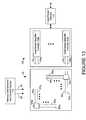
- FIGS. 5A and 5Bare schematic block diagrams of embodiments of the data sense and write circuitry, in conjunction with a memory cell array and input/output circuitry, according certain aspects of the present inventions;
- FIG. 6is a block diagram representation of a memory cell array, including a plurality of memory cells (for example, the memory cells illustrated in FIGS. 1A-3B ) in conjunction with data sense and write circuitry, according an embodiment of the present inventions;
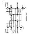
- FIG. 7is a schematic representation of a first embodiment of the data sense amplifier circuitry, including a sense amplifier latch, bit line input circuitry and write back circuitry, in conjunction with input/output circuitry, according certain aspects of the present inventions;
- FIG. 8is a schematic representation of reference current generation circuitry, which may be employed with the data sense amplifier circuitry of FIG. 7 , in accordance with certain aspects of the present inventions;
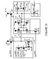
- FIGS. 9A-9Care schematic representations of write back circuitry, which may be employed with the data sense amplifier circuitry of FIG. 7 , in accordance with certain aspects of the present inventions;
- FIG. 10is a schematic representation of another embodiment of the data sense amplifier circuitry, including a sense amplifier latch, bit line input circuitry and write back circuitry, in conjunction with input/output circuitry, according certain aspects of the present inventions;
- FIG. 11is a schematic representation of reference current generation circuitry, which may be employed with the data sense amplifier circuitry of FIG. 10 , in accordance with certain aspects of the present inventions;
- FIGS. 12A and 12Bare illustrative examples of two-transistor memory cells
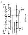
- FIG. 13is a block diagram representation of a first embodiment of a memory cell array, including a plurality of two-transistor memory cells (for example, the memory cell illustrated in FIG. 12A ) in conjunction with data sense circuitry according to an embodiment of the present inventions;
- FIG. 14is a schematic representation of a first embodiment of a data sense amplifier circuitry that may be implemented in conjunction with a two-transistor memory cell array, according certain aspects of the present inventions;
- FIGS. 15A and 15Bare schematic representations of write back circuitry, which may be employed with the data sense amplifier circuitry of FIG. 14 , in accordance with certain aspects of the present inventions;
- FIG. 16is a schematic representation of a first embodiment of the data sense amplifier circuitry, including a sense amplifier latch and bit line input circuitry (but not write back circuitry), that may be implemented in conjunction with a memory cell array including a plurality of memory cells, each having a PMOS or P-channel type transistor, like that illustrated in FIGS. 1A-3B , according certain aspects of the present inventions;
- FIG. 17is a schematic representation of reference current generation circuitry (not including write back circuitry), which may be employed with the data sense amplifier circuitry of FIG. 16 , in accordance with certain aspects of the present inventions;
- FIG. 18is a schematic representation of another embodiment of the data sense amplifier circuitry, including a sense amplifier latch, bit line input circuitry and write back circuitry, that may be implemented in conjunction with a memory cell array including a plurality of memory cells, each having a PMOS or P-channel type transistor of the type illustrated in FIGS. 1A-3B (electrically floating body transistors), according to certain aspects of the present inventions;
- FIG. 19is a schematic representation of reference current generation circuitry (excluding write back circuitry), which may be employed with the data sense amplifier circuitry of FIG. 16 , in accordance with certain aspects of the present inventions;
- FIG. 20is a schematic representation of data sense amplifier circuitry, including a sense amplifier latch that may be implemented with a memory cell array, having a plurality of two-transistor P-channel type or PMOS memory cells (for example, the memory cell illustrated in FIG. 12B ), according certain aspects of the present inventions;
- FIG. 21is a schematic representation of reference current generation circuitry (excluding write back circuitry), having a configuration that facilitates testing of certain circuitry of data sense amplifier circuitry, in accordance with certain aspects of the present inventions;
- FIGS. 22A, 22B and 23are schematic representations of memory cell array(s), including a plurality of memory cells (for example, the memory cells illustrated in FIGS. 1A-3B ) in conjunction with data sense circuitry, according to various embodiments of the present inventions;
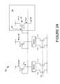
- FIG. 24is a schematic representation of one embodiment of one aspect of the circuitry and techniques for adjusting, setting, determining, controlling and/or generating a reference current, using a MOS transistor “ratioing” configuration, as described and illustrated in U.S. Provisional Patent Application Ser. No. 60/718,417, for one aspect of the data sense amplifier circuitry of the present inventions;
- FIG. 25is a schematic representation of one embodiment of one aspect of the circuitry and techniques for adjusting, setting, determining, controlling and/or generating a reference current, using the state of a control bit to a plurality of pair of reference cells in order to implement a digital control of the reference current level (employed during a read operation), as described and illustrated in U.S. Provisional Patent Application Ser. No. 60/718,417, for one aspect of the data sense amplifier circuitry of the present inventions; and
- FIG. 26is a schematic block diagram of an embodiment of the data sense and write circuitry, having a voltage level shifter incorporated in the write-back circuitry path, in conjunction with a memory cell array and input/output circuitry, according certain aspects of the present inventions.
- the present inventionsare directed to a technique of, and circuitry for sampling, sensing, reading and/or determining the data state of a memory cell of a memory cell array (for example, a memory cell array having a plurality of memory cells which consist of an electrically floating body transistor).
- the present inventionsinclude sense amplifier circuitry that is relatively compact and pitched to the array of memory cells such that a row of data may be read, sampled and/or sensed during a read operation.
- an entire row of memory cellsmay be accessed and read during one operation which, relative to at least architecture employing multiplexer circuitry, may minimize, enhance and/or improve read latency and read access time, memory cell disturbance and/or simplify the control of the sense amplifier circuitry and access thereof.
- the sense amplifier circuitryalso includes write back circuitry to modify or “re-store” the data read, sampled and/or sensed during a read operation or a refresh operation in the context of a DRAM array.
- the sense amplifier circuitry of this embodimentrestores or refreshes data in an entire row of volatile and/or destructive read type memory cells in parallel which, relative to at least architecture employing multiplexer circuitry, may minimize, enhance and/or improve write back and read latency parameters.
- data that has been read, sampled and/or sensed by the sense amplifier circuitry during a read operationmay be modified before being written back to one or more of the memory cells of the selected row of the array of memory cells.
- the present inventionsmay be implemented in conjunction with any memory cell technology that generates at least two current values (each current being representative of, for example, a respective data state).
- the memory technologymay be an electrically floating body transistor (P-channel or N-channel type transistors) described above or any other technology whether now known or later developed. Indeed, all such memory technologies are considered to fall within the scope of the present inventions.
- the present inventionsinclude data sense circuitry 100 coupled to memory cell array 10 .
- the data sense circuitry 100includes data sense amplifier circuitry 102 which is controllable and/or selectively connected to each bit line 32 of memory cell array 10 .
- the data sense amplifier 102includes sense amplifier latch 104 reference current input circuitry 106 , and bit line input circuitry 114 .
- sense amplifier latch 104samples, senses, reads and/or determines the data state of a memory cell disposed on row line 28 that is connected to the associated data sense amplifier 102 .
- the reference current input circuitry 106applies a reference current, generated by or in reference to current generation circuitry 108 , and to data sense amplifier circuitry 102 .
- data sense amplifier circuitry 102compares the current conducted by memory cell 12 with the reference current generated by reference current generation circuitry 108 in sensing, sampling and/or determining the data of the selected memory cells 12 .
- the magnitude of the reference currentgenerally lies between the magnitudes of the currents conducted in the logic high data state and logic low data state of memory cell 12 .
- input/output circuitry 110facilitates external access to memory cells 12 of memory cells array 10 via sense amplifier circuitry 102 .
- datamay be stored in and/or output from a row of memory cells 12 by selectively and controllably enabling input/output circuitry 110 associated with sense amplifier circuitry 102 .
- the input/output circuitry 110may include pass gates and/or column switch circuitry to facilitate and/or implement the read and write operations to memory cells 12 .
- the memory cell selection circuitry 112may control the connection of a selected row of memory cells 12 of memory cell array 10 to data sense amplifier circuitry 102 .
- memory cell selection and control circuitry 112may be a conventional word line and bit line decoder or driver.
- control signal generation circuitryto selectively apply predetermined voltage signals to word lines 28 and source lines 30 .
- pass gates and/or row switch circuitrymay be employed to selectively activate a transistor of memory cell 12 connected to data sense amplifier circuitry 102 to facilitate and/or implement the read operation of memory cell 12 .
- data sense circuitry 100may include write back circuitry 116 to modify or “re-store” the data read, sampled and/or sensed during a read operation or a refresh operation in the context of an array of volatile and/or destructive read type memory cells 12 . As such, in this embodiment, data sense circuitry 100 restores or refreshes data in an entire row of memory cells 12 in parallel.
- the write back circuitry 116will be described in more detail below.
- data sense amplifier circuitry 102includes sense amplifier latch 104 having input node SA, coupled to bit lines 32 , via bit line input circuitry 114 , and input node SAB, connected to reference current input circuitry 106 .
- input nodes SA and SABare equilibrated to and maintained at a source voltage (in the illustrated example, V SS ) while transistors 142 , 144 a and 144 b are biased at a reference voltage or voltages via signal lines 146 and 148 .
- the reference voltages on lines 146 and 148clamp the voltages (here, the high voltage level) on bit lines 32 , BLREF 0 and BLREF 1 respectively.
- the nodes 118 and 120attain predetermined sensing voltages when a predetermined memory cell 12 is turned on (via memory cell selection and control circuitry 112 applying a predetermined read control signal on a corresponding memory cell 12 ). Thereafter, node 122 is released, by turning off transistors 124 a and 124 b (via application of control signal EQSA having suitable voltage and timing). This configuration allows a differential voltage on input nodes SA and SAB to develop based on the charging currents (or discharging currents) supplied by transistors 126 and 128 . Finally, transistors 142 , 144 a and 144 b are turned off after sense amplifier latch 104 is latches a data state.
- the current supplied or provided by transistor 126is mirrored from the selected memory cell 12 .
- the activated memory cell 12is connected to bit line 32 , which is associated with a particular sense amplifier latch 104 .
- the current supplied or provided by transistor 128is mirrored from the current provided by reference current generation circuitry 108 .
- the current supplied by reference current generation circuitry 108is equal to or substantially equal to one-half of the summation of the currents in a first reference cell, which has a logic low data state, and a second reference cell, which has a logic high data state.
- the currents output or provided by transistors 126 and 128charge the intrinsic capacitances of input nodes SA and SAB thereby providing or producing a differential voltage therebetween.
- the sense amplifier latch 104(comprised of transistors 130 - 136 which are arranged in a cross-coupled configuration) amplifies the difference to provide a first voltage at one of the input nodes (SA or SAB) and the complementary voltage at the other input node. The larger of the two currents will charge the respective input node of sense amplifier latch 104 to a higher voltage level.
- transistor 126provides more current than transistor 128 and, as such, input node SA of sense amplifier latch 104 is amplified to the first supply potential (in the illustrated embodiment, V DSA ) and input node SAB is pulled or brought to the second supply potential (in the illustrated embodiment, V SS ).
- transistor 134turns on to “pull” input node SAB low, which turns transistor 130 off and turns transistor 132 on.
- input node SAis pulled to the first supply potential (in the illustrated embodiment, V DSA ) when transistor 138 is turned on via signal line 140 .
- transistor 132does not turn on until transistor 138 turns on.
- signal STRSABon signal line 140 ) may be pulsed low before input node SAB is above a threshold voltage level.
- transistor 130turns on to “pull” input node SA low, which turns transistor 134 off and turns transistor 136 on. Notably, transistor 136 does not turn on until transistor 138 turns on. Under these circumstances and when transistor 138 is turned on via signal line 140 (STRSAB may be pulsed low before input node SAB is above a threshold voltage level), input node SAB is pulled to the first supply potential (in the illustrated embodiment, V DSA ).
- Vtthreshold voltage
- the voltage on input node SABwill be about twice the voltage relative to the voltage on node SA because input node SAB has twice the current to charge up the same or substantially similar node capacitances.
- transistors 126 and 128are designed to have the same or substantially similar drain to source bias, a current mirror may be employed.
- sense amplifier latch 104After sense amplifier latch 104 senses, samples and/or determines the data state of the selected memory cell, the data state of the selected memory cell is stored in sense amplifier latch 104 by turning off transistors 142 , 144 a and 144 b via applying control signals, having a logic low, on signal lines 146 and 148 , respectively. The data may be read or accessed from sense amplifier latch 104 via pass gates 150 a and 150 b of input/output circuitry 110 .
- the first voltagemay be a first supply potential (in the illustrated embodiment, V DSA ) and the second voltage may be a second supply potential (in the illustrated embodiment, V SS ).
- the specific voltages of the first and second supply potentialsmay be determined based on programming or writing operation considerations or requirements of memory cell 12 .
- data sense amplifier circuitry 102also includes write back circuitry 116 to modify or “re-store” the data read, sampled and/or sensed during a read operation or a refresh operation in the context of a DRAM memory cell array (for example, a plurality of N-channel or NMOS electrically floating body transistors).
- the write back circuitry 116generates the correct bit line voltage based on the data stored in sense amplifier latch 104 to program the selected or predetermined memory cell 12 to the appropriate data state (for example, the data state that existed prior to reading the memory cell or for example, data that has been written to the sense amplifier latch using input/output circuitry 110 ).
- a row of memory cells 12is first read, sampled and/or sensed so that bit cell data is copied to sense amplifier latches 104 of sense amplifier circuitry 100 .
- Selected latches in sense amplifier circuitry 100are then overwritten by the application of new data via pass gates 150 a and 150 b of input/output circuitry 110 .
- data in sense amplifier latches 104 of sense amplifier circuitry 100is written back into memory cells 12 of the selected row of memory cell array 10 by way of write back circuitry 116 .
- “write back reference”is that circuitry which generates the appropriate voltages for writing the reference cells.
- two memory reference cellsare employed such that one memory cell stores a “0” data state and the other memory cell stores a “1” data state.
- REFDATAis changed from low to high, the states of the two memory reference cells are swapped or changed to the opposite data state. This technique may enhance or improve the reliability of the memory array in that it will minimize the situation where a particular memory cell is continuously programmed with the same data state.
- write back circuitry 116may be configured in various embodiments (employing different numbers of transistors) that are suitable for generating the appropriate voltages for the selected memory cell technology.
- the complimentary outputs SA and SAB of sense amplifier latch 104determine if the voltages appropriate to write data state “1” or the voltages appropriate to write data state “0” are applied to bit line 32 .
- Control signals WR 0 , WR 0 b , WR 1 , and WR 1 bare global signals that connect to write back circuitry 116 for all of data sense amplifier circuitry 102 .
- Signal WR 0is generated by inverting WR 0 b
- WR 1is generated by inverting WR 1 b.
- write back circuitry 116may be “customized” to generate the bit line voltages suitable to program the memory cell of the selected memory technology.
- the memory technologymay be an electrically floating body transistor described above or any other technology whether now known or later developed. Accordingly, all such write back circuitry, whether now known or later developed should be considered to fall within the scope of the present inventions.
- data sense amplifier circuitry 102is coupled to memory cell array 10 (for example, including a plurality of memory cells each having an N-channel type electrically floating body transistor).
- data sense amplifier circuitry 102modifies, senses, samples and/or reads the data state of a predetermined or selected memory cell via transistor 152 (in contrast to the current mirror configuration of FIG. 7 ). Since the current on bit line 32 tends to pull towards the second supply voltage (V SS ), data sense amplifier circuitry 102 is equilibrated to the first supply voltage (V DSA ). Thereafter, the EQSAB signal is released after node 154 reaches a sensing voltage with the selected word line 28 turned on.
- the input nodes SA and SAB of sense amplifier latch 104are released from the first supply voltage (V DSA ) after node 154 reaches its sensing voltage thereby permitting or allowing a differential voltage on input nodes SA and SAB of sense amplifier latch 104 to develop based on the charging currents (or discharging currents) supplied by transistor 152 (provided or produced in response to the output of the selected memory cell 12 ) and transistor 156 (provided or produced in response to the output of reference current generation circuitry 108 ).
- the current generated or provided by transistor 156is current mirrored from the current supplied by reference current generation circuitry 108 (via transistors 158 - 162 ), which is half of the summation of the currents in the two reference cells.
- the current supplied by reference current generation circuitry 108is substantially equal to one-half of the summation of the currents in a first reference cell, which has a logic low data state, and a second reference cell, which has a logic high data state.
- the currents provided by transistors 152 and 156discharge the intrinsic capacitances of input nodes SA and SAB thereby providing or producing a differential voltage between the two input nodes of sense amplifier latch 104 .
- the greater of the two currentswill discharge its corresponding input node further and faster from the first supply voltage (illustrated in this exemplary embodiment as V DSA ) than the other input node.
- Vtthreshold voltage
- transistor 132turns on and thereby pulls the voltage of input node SAB to the first supply voltage.
- input node SABis the first node to fall a threshold voltage (Vt) level below first supply voltage
- transistor 136turns on and thereby pulls the voltage of input node SA to the first supply voltage.
- sense amplifier latch 104stores the data state of the selected memory cell therein by turning off transistors 152 , 144 a and 144 b via applying control signals, having a logic low, on signal lines 146 and 148 , respectively.
- the datamay be read or accessed from sense amplifier latch 104 via pass gates 150 a and 150 b of input/output circuitry 110 .
- the present inventionsare directed to a technique of, and circuitry for modifying, sampling, sensing, reading and/or determining the data state of a memory cell implementing two transistors which store complementary data states. That is, the two-transistor memory cell includes a first transistor that maintains a complementary state relative to the second transistor. As such, when programmed, one of the transistors of the memory cell stores a logic low (a binary “0”) and the other transistor of the memory cell stores a logic high (a binary “1”).
- the data state of the two-transistor complementary memory cellis read and/or determined by sampling, sensing measuring and/or detecting the polarity of the logic states stored in each transistor of complementary memory cell. That is, the two-transistor complementary memory cell is read by sampling, sensing, measuring and/or detecting the difference in current output by the two transistors.
- the two-transistor complementary memory cellis described and illustrated in U.S. patent application Ser. No. 10/829,877, which was filed by Ferrant et al. on Apr. 22, 2004, and entitled “Semiconductor Memory Cell, Array, Architecture and Device, and Method of Operating Same”. For the sake of brevity, those discussions will not be repeated here; rather, the entire contents of the non-provisional U.S. patent application, including, for example, the inventions, features, attributes, architectures, layouts, configurations, materials, techniques and advantages described and illustrated therein, are hereby incorporated by reference herein.
- data sense amplifier circuitry 102is controllable and/or selectively connected to an associated pair of two-transistor memory cells 12 of array 10 (wherein the memory transistors are NMOS transistors).
- data sense circuitry 100does not include reference current input circuitry 106 and reference current generation circuitry 108 . Rather, data sense amplifier 102 receives two inputs/outputs (for example, bit lines 32 a 1 and 32 a 2 ) of two-transistor memory cells 12 .
- a first input/output of two-transistor memory cells 12is provided to input node SA of sense amplifier latch 104 (via transistor 164 ) and a second input/output of two-transistor memory cells 12 is provided to input node SAB of sense amplifier latch 104 (via transistor 166 ).
- the currents provided by transistors 164 and 166(which are responsive to the data state of the transistors of two-transistor memory cells 12 ) discharge the intrinsic capacitances of input nodes SA and SAB, previously pre-charged at VDSA potential by transistors P 0 and P 1 , thereby providing or producing a differential voltage therebetween.
- the sense amplifier latch 104(comprised of transistors 130 - 136 which are arranged in a cross-coupled configuration) amplifies the difference to provide a first voltage at one of the input nodes (SA or SAB) and the complementary voltage at the other input node. The larger of the two currents will discharge the respective input node of sense amplifier latch 104 to a lower voltage level.
- transistor 164provides more current than transistor 166 and, as such, input node SA of sense amplifier latch 104 is amplified to the first source potential (in the illustrated embodiment, V SS ) and input node SAB is pulled or brought to the second source potential (in the illustrated embodiment, V DSA ).
- the larger of the two currentswill “pull” its respective input node to a lower voltage since, in the exemplary embodiment, sense amplifier latch 104 is equilibrated to a voltage of V DSA .
- sense amplifier latch 104The operation of sense amplifier latch 104 is substantially similar to the operation of sense amplifier latch 104 described above with respect to FIG. 10 . That is, after sense amplifier latch 104 senses, samples and/or determines the data state of the selected memory cell, that data state is stored in sense amplifier latch 104 by turning off transistors 164 and 166 via applying control signal (BLCLAMP) on signal line 168 . The data may be read or accessed from sense amplifier latch 104 via pass gates 150 a and 150 b of input/output circuitry 110 (via signal YSEL).
- BLCLAMPcontrol signal
- write back circuitry 116uses the data state stored in sense amplifier latch 104 to select the appropriate bit line voltages to program the two-transistors 14 a and 14 b of selected memory cell 12 connected to a bit line pair.
- a detailed schematic illustration of suitable write back circuitry 116is illustrated in FIGS. 15A and 15B . Because the bit line currents tend to pull toward the second source voltage (illustrated in this example as V SS ), it may be advantageous to equilibrate sense amplifier latch 104 to the first source voltage (illustrated in this example as V DSA ).
- the present inventionsmay also be implemented in conjunction with a PMOS or P-channel memory array.
- data sense circuitry 100may adopt similar architectures and/or configurations of as described above with respect to NMOS or N-channel memory arrays.
- memory cell array 10includes memory cells 12 which are each comprised of an electrically floating body PMOS or P-channel transistor 14
- data sense circuitry 100may be configured as illustrated in FIGS. 16 and 17 . The operation of data sense circuitry 100 of FIGS.
- data sense circuitry 100may be configured as illustrated in FIGS. 18 and 19 .
- the operation of data sense circuitry 100 of FIGS. 18 and 19including the operation of data sense amplifier circuitry 102 and reference current generation circuitry 108 , is apparent to one skilled in the art, in light of this disclosure, and is similar to the operation of data sense circuitry 100 illustrated in FIGS. 7, 10 and 11 . Again, for sake of brevity, those discussions will not be repeated.
- data sense circuitry 100may be configured as illustrated in FIG. 20 .
- the operation of data sense circuitry 100 of FIG. 20is apparent to one skilled in the art, in light of this disclosure, and is similar to the operation of data sense circuitry 100 illustrated in FIG. 14 . Again, for sake of brevity, those discussions will not be repeated.
- data sense amplifier circuitry 102may include write back circuitry 116 to modify or “re-store” the data read, sampled and/or sensed during a read operation or a refresh operation in the context of a DRAM array.
- sense amplifier circuitry 102would modify or re-store or refresh data in an entire row of volatile and/or destructive read type memory cells in parallel which, relative to an architecture employing multiplexer circuitry, may minimize enhance and/or improve write back and read latency parameters.
- the reference current generation circuitry 108 illustrated hereinis connected and provides a reference current to sense amplifier latch 104 of a plurality of data sense amplifier circuitry 102 . (See, for example, FIG. 6 ). Moreover, reference current generation circuitry 108 employs signal BLCLAMPREF to facilitate margin testing of data sense amplifier circuitry 102 . In this regard, margin testing may be performed by clamping the reference bit lines at either higher or lower voltages than in normal operating conditions. For example, memory cell 12 may be read, sampled and/or sensed during a read operation or a refresh operation with BLCLAMPREF at a different voltage than BLCLAMP when these two signals are at their reference values.
- test modeallows all of the reference currents to be set by an external pin to permit testing of some or all of the circuitry of data sense amplifier circuitry 102 .
- transistor 170 of bit line input circuitry 114may be used to short bit line 32 to a VEQBL voltage—thereby facilitating testing.
- VEQBLis 0V when a particular word line 18 is unselected (i.e., off) and about 300 mV when word line is selected (i.e., on).
- the access timemay be improved because the amount of time required for nodes 118 and PREF to attain appropriate sensing voltages may be shortened by having VEQBL at 300 mV during a read operation or a refresh operation.
- VEQBLremains at, for example, 300 mV and transistor 170 is only turned on during a read operation or a refresh operation.
- BLCLAMPREFis driven low for EXTREF to set the PREF current.
- the present inventionsmay be implemented in conjunction with any memory technology that generates at least two current values (representative of, for example, a respective data state).
- the memory technologymay be an electrically floating body transistor described above or any other technology whether now known or later developed. All such memory technologies are considered to fall within the scope of the present inventions.
- an integrated circuit or memory devicemay include a plurality of memory cell arrays 10 a - x , each having corresponding data sense circuitry 100 a - x .
- adjacent arrays 10 a and 10 bmay share data sense circuitry 100 a .
- memory array 10may include a layout whereby a portion of array 10 is connected to data sense circuitry 100 a and the remaining portion of array 10 is connected to data sense circuitry 100 b .
- the integrated circuit or memory devicemay include a plurality of arrays 10 a - 10 d , each connected to data sense circuitry 100 a - 100 d , respectively.
- the data sense circuitry 100 a - 100 dmay be located or disposed near the center of the associated arrays 10 a - 10 d , respectively. (See, for example, FIG. 23 ).
- the memory cellsmay be arranged, configured and/or controlled using any of the memory cell arrays, architectures and/or control/operation techniques.
- the memory cellsmay be arranged, configured and/or controlled using any of the memory cell arrays, architectures and/or control/operation techniques described and illustrated in the following provisional and non-provisional U.S. patent applications:
- the memory cellsmay be controlled (for example, programmed or read) using any of the control circuitry described and illustrated in the above-referenced U.S. patent applications.
- memory cell selection and control circuitry 112may be implemented as described and illustrated in the above-referenced U.S. patent applications.
- control circuitryis incorporated herein by reference. Indeed, all such control/selection techniques and circuitry therefor, whether now known or later developed, are intended to fall within the scope of the present inventions.
- the electrically floating memory cells, transistors and/or memory array(s)may be fabricated using well known techniques and/or materials. Indeed, any fabrication technique and/or material, whether now known or later developed, may be employed to fabricate the electrically floating memory cells, transistors and/or memory array(s). For example, the present inventions may employ silicon (whether bulk-type or SOI), germanium, silicon/germanium, gallium arsenide or any other semiconductor material in which transistors may be formed. Indeed, the electrically floating transistors, memory cells, and/or memory array(s) may employ the techniques described and illustrated in non-provisional patent application entitled “Integrated Circuit Device, and Method of Fabricating Same”, which was filed on Jul. 2, 2004, by Fazan, application Ser. No.
- Integrated Circuit Device Patent Application10/884,481 (hereinafter “Integrated Circuit Device Patent Application”).
- Integrated Circuit Device Patent ApplicationThe entire contents of the Integrated Circuit Device Patent Application, including, for example, the inventions, features, attributes, architectures, configurations, materials, techniques and advantages described and illustrated therein, are hereby incorporated by reference herein.
- memory array 10may be integrated with SOI logic transistors, as described and illustrated in the Integrated Circuit Device Patent Application.
- an integrated circuit deviceincludes memory section (having, for example, PD or FD SOI memory transistors 14 ) and logic section (having, for example, high performance transistors, such as FinFET, multiple gate transistors, and/or non-high performance transistors (for example, single gate transistors that do not possess the performance characteristics of high performance transistors—not illustrated)).
- memory sectionhaving, for example, PD or FD SOI memory transistors 14
- logic sectionhaving, for example, high performance transistors, such as FinFET, multiple gate transistors, and/or non-high performance transistors (for example, single gate transistors that do not possess the performance characteristics of high performance transistors—not illustrated)).
- the electrically floating memory cells, transistors and/or memory array(s)may be fabricated on, in and/or with strained silicon.
- fabrication of the floating memory cells, transistors and/or memory array(s) according to the present inventionsmay employ the techniques described and illustrated in Provisional U.S. patent application entitled “One Transistor Memory Cell having Mechanically Strained Electrically Floating Body Region, and Method of Operating Same”, which was filed on Oct. 19, 2005, by Bassin, Application Ser. No. 60/728,060.
- the entire contents of Application Ser. No. 60/728,060including, for example, the inventions, features, attributes, architectures, configurations, materials, techniques and advantages described and illustrated therein, are hereby incorporated by reference herein.
- the memory arraysmay be comprised of N-channel, P-channel and/or both types of transistors, as well as partially depleted and/or fully depleted type transistors.
- circuitry that is peripheral to the memory arraymay include fully depleted type transistors (whether P-channel and/or N-channel type).
- circuitrymay include partially depleted type transistors (whether P-channel and/or N-channel type).
- present inventionsmay be employed or implemented in conjunction with one or more of the inventions, memory arrays and memory devices, and techniques for programming, reading, controlling and/or operating a semiconductor memory cell, array and device of the following provisional U.S. patent applications:
- electrically floating body transistor 14may be a symmetrical or non-symmetrical device. Where transistor 14 is symmetrical, the source and drain regions are essentially interchangeable. However, where transistor 14 is a non-symmetrical device, the source or drain regions of transistor 14 have different electrical, physical, doping concentration and/or doping profile characteristics. As such, the source or drain regions of a non-symmetrical device are typically not interchangeable. This notwithstanding, the drain region of the electrically floating N-channel transistor of the memory cell (whether the source and drain regions are interchangeable or not) is that region of the transistor that is connected to the bit line/sense amplifier.
- the inventionsare entirely applicable to N-channel and/or P-channel transistors.
- the discussion described and illustratedonly source and drain implants, other implants may also be included.
- implants to modify the operation of memory cells 12which affect, for example, the power consumption of memory cells 12 as described and illustrated in (1) application Ser. No. 10/450,238, which was filed on Jun. 10, 2003 and entitled “Semiconductor Device”, (2) application Ser. No. 10/487,157, which was filed on Feb. 18, 2004 and entitled “Semiconductor Device”; and Provisional Application Ser. No. 60/578,631, which was filed on Jun. 10, 2004 and entitled “Asymmetrical Electrically Floating Body Memory Device, and Method of Manufacturing Same”.
- reference current generation circuitry 108is described in the context of supplying a reference current that is substantially equal to one-half of the summation of the currents in a first reference cell, which has a logic low data state, and a second reference cell, which has a logic high data state, other circuitry and techniques may be employed to generate the reference currents used by sense amplifier latch 104 to sense, sample and/or determine the data state of a selected memory cell 12 . Indeed, all such reference current generation techniques and circuitry therefor, whether now known or later developed, are intended to be within the scope of the present inventions.
- circuitry and techniques described and illustrated in non-provisional patent application entitled “Reference Current Generator, and Method of Programming, Adjusting and/or Operating Same”, filed May 7, 2004 by Portmann et al., and assigned Ser. No. 10/840,902,may be employed to generate an appropriate reference current for data sense amplifier circuitry 102 .
- the entire contents of U.S. Patent application Ser. No. 10/840,902, including, for example, the inventions, features, attributes, architectures, configurations, materials, techniques and advantages described and illustrated therein,are hereby incorporated by reference herein.
- the present inventionsmay employ the circuitry and techniques for generating a reference current for data sense amplifier circuitry 102 as described and illustrated in U.S. Provisional Patent Application Ser. No. 60/718,417, which was filed by Bauser on Sep. 19, 2005, and entitled “Method and Circuitry to Generate a Reference Current for Reading a Memory Cell Having an Electrically Floating Body Transistor, and Device Implementing Same”. (See, for example, FIGS. 24 and 25 ).
- the entire contents of U.S. Provisional Patent Application Ser. No. 60/718,417, including, for example, the inventions, features, attributes, architectures, configurations, materials, techniques and advantages described and illustrated therein,are hereby incorporated by reference herein.
- the present inventionsmay employ the circuitry and techniques for independently controlling certain parameters (for example, temporal or voltage), for a memory operation (for example, restore, write, refresh), to program or write a predetermined data state into a memory cell (for example, programming or writing data state “1” or “0” into a memory cell) as described and illustrated in U.S. Provisional Patent Application Ser. No. 60/731,668, which was filed by Popoff on Oct. 31, 2005, and entitled “Method and Apparatus for Varying the Programming Duration of a Floating Body Transistor, and Memory Cell, Array, and/or Device Implementing Same”.
- certain parametersfor example, temporal or voltage
- a memory operationfor example, restore, write, refresh
- program or write a predetermined data state into a memory cellfor example, programming or writing data state “1” or “0” into a memory cell
- the duration of programming/writing of a given memory state into a memory cell by data sense amplifier circuitry 102may be controlled adjusted, determined and/or predetermined according to or based on the given memory operation (for example, restore, write, refresh).
- the voltage conditions applied to the memory cell for programming/writing a given memory state into a memory cell by data sense amplifier circuitry 102may be controlled and/or adjusted according to the memory operation (for example, restore, write, refresh).
- the illustrated/exemplary voltage levels applied to the electrically floating body memory cells which implement the read and write operationsare merely exemplary.
- the indicated voltage levelsmay be relative or absolute.
- the voltages indicatedmay be relative in that each voltage level, for example, may be increased or decreased by a given voltage amount (for example, each voltage may be increased by 0.5 volts) whether one or more of the voltages (for example, the source, drain or gate voltages) become or are positive and negative.
- the present inventionsmay be implemented in conjunction with a voltage level shifter in the write-back circuitry path. (See, FIG. 26 ).
- the voltage levels applied to the memory cellsmay be different than the voltage levels pertaining to the sense amplifier latch 104 .
- All voltage level shifting techniques and circuitry therefor, whether now known or later developed,are intended to be within the scope of the present inventions.
- each of the aspects of the present inventions, and/or embodiments thereofmay be employed alone or in combination with one or more of such aspects and/or embodiments.
- those permutations and combinationswill not be discussed separately herein.
- the present inventionsare neither limited to any single aspect (nor embodiment thereof), nor to any combinations and/or permutations of such aspects and/or embodiments.
Landscapes
- Engineering & Computer Science (AREA)
- Microelectronics & Electronic Packaging (AREA)
- Computer Hardware Design (AREA)
- Semiconductor Memories (AREA)
- Dram (AREA)
- Read Only Memory (AREA)
Abstract
Description
- This application claims priority to U.S. Provisional Application Ser. No. 60/635,709, entitled “Sense Amplifier Circuitry and Architecture to Write Data Into and/or Read from Memory Cells”, filed Dec. 13, 2004. The contents of this provisional application are incorporated by reference herein in their entirety.
- The inventions relate to semiconductor integrated circuit devices (for example, memory devices); and more particularly, in one aspect, to circuitry and techniques to write and read, sense and/or sample a data state to/from memory cells of a memory array and/or device, for example, a semiconductor dynamic random access memory (“DRAM”) device, wherein the memory cells have an electrically floating body in which an electrical charge is stored.
- There is a continuing trend to employ and/or fabricate advanced integrated circuits using techniques, materials and devices that improve performance, reduce leakage current and enhance overall scaling. Silicon-on-Insulator (SOI) is a material in which such devices may be fabricated on or in (hereinafter collectively “on”). Such devices are known as SOI devices and include, for example, partially depleted (PD), fully depleted (FD) devices, multiple gate devices (for example, double or triple gate), and Fin-FET. SOI devices have demonstrated improved performance (for example, speed), reduced leakage current characteristics and considerable enhancement in scaling.
- One type of DRAM memory cell is based on, among other things, a floating body effect of SOI transistors. (See, for example, U.S. patent application Ser. No. 10/450,238, Fazan et al., filed Jun. 10, 2003 and entitled “Semiconductor Device”, hereinafter “Semiconductor Memory Device Patent Application”). In this regard, the memory cell may consist of a PD or a FD SOI transistor (or transistor formed in bulk material/substrate) having a gate dielectric, which is disposed adjacent to the body and separated therefrom by a channel. The body region of the transistor is electrically floating in view of the insulation or non-conductive region (for example, in bulk-type material/substrate) disposed beneath the body region. The state of the memory cell is determined by the concentration of charge within the body region of the SOI transistor.
- With reference to
FIGS. 1A, 1B and1C, in one embodiment, semiconductormemory cell array 10 includes a plurality ofmemory cells 12 each consisting oftransistor 14 havinggate 16,body region 18, which is electrically floating,source region 20 anddrain region 22. Thebody region 18 is disposed betweensource region 20 and drainregion 22. Moreover,body region 18 is disposed on or aboveregion 24, which may be an insulation region (for example, in SOI material/substrate) or non-conductive region (for example, in bulk-type material/substrate). The insulation or non-conductive region may be disposed on or insubstrate 26. - Data is written into or read from a selected memory cell by applying suitable control signals to selected word line(s)28, selected source line(s)30 and/or selected bit line(s)32. In response, charge carriers are accumulated in or emitted and/or ejected from electrically floating
body region 18 wherein the data states are defined by the amount of carriers within electrically floatingbody region 18. Notably, the entire contents of the Semiconductor Memory Device Patent Application, including, for example, the features, attributes, architectures, configurations, materials, techniques and advantages described and illustrated therein, are incorporated by reference herein. - As mentioned above,
memory cell 12 ofarray 10 operates by accumulating in or emitting/ejecting majority carriers (electrons or holes)34 frombody region 18 of, for example, an N-channel transistor. (See,FIGS. 2A and 2B ). In this regard, accumulating majority carriers (in this example, “holes”)34 inbody region 18 ofmemory cells 12 via, for example, impact ionization nearsource region 20 and/ordrain region 22, is representative of a logic high or “1” data state. (See,FIG. 2A ). Emitting or ejectingmajority carriers 34 frombody region 18 via, for example, forward biasing the source/body junction and/or the drain/body junction, is representative of a logic low or “0” data state. (See,FIG. 2B ). - Notably, for at least the purposes of this discussion, a logic high or State “1” corresponds to an increased concentration of majority carries in the body region relative to an unprogrammed device and/or a device that is programmed with a logic low or State “0”. In contrast, a logic low or State “0” corresponds to a reduced concentration of majority carries in the body region relative to an unprogrammed device and/or a device that is programmed with a logic high or State “1”.
- As mentioned above, conventional techniques to write or program a logic low (State “0”) in
memory cell 12 may be accomplished by removing majority carriers frombody region 18 through eithersource region 20 ordrain region 22 of electrically floatingbody transistor 14 ofmemory cell 12. In this regard, in one embodiment, majority carriers (in this example, “holes”)34 inbody region 18 ofmemory cells 12 are removed frommemory cell 12 throughdrain region 22. (See,FIG. 3A ). A positive current36 (electrons flowing in opposite direction) flows fromdrain region 22 tosource region 20 due to a channel forming in a portion ofbody region 18 immediately beneathgate oxide 38 when writing or programming a logic low (State “0”). Where the majority carriers (in this example, “holes”)34 are removed frommemory cell 12 throughsource region 20, positive current36 (electrons flowing in opposite direction) flows fromsource region 20 to drainregion 22 as a result of channel formation when writing or programming a logic low (State “0”). (See,FIG. 3B ). - Conventional techniques may employ a two-cycle write or program technique to store a desired data state in
memory cells 12. In this regard, in one embodiment, in the first cycle a logic low (State “0”) is written into allmemory cells 12 connected toword line 28; in the second cycle, a logic high (State “1”) is selectively written intomemory cells 12 while an inhibit signal or voltage is applied to thosememory cells 12 that are to maintain a logic low or State “0”. In this way,certain memory cells 12 connected to a given word line may be written or programmed to a logic low (State “0”) using a first word line voltage; and certainother memory cells 12, also connected to the given word line, may be written or programmed to a logic high (State “1”) using a second word line voltage. (See, for example, application Ser. No. 10/840,009, which was filed by Ferrant et al. on May 6, 2004, and entitled “Semiconductor Memory Device and Method of Operating Same”). - Several techniques may be implemented to read the data stored in the memory cell. For example, a current sense amplifier may be employed to read the data stored in memory cells. In this regard, a current sense amplifier may compare the cell current to a reference current, for example, the current of a reference cell. From that comparison, it may be determined whether the memory cell contained a logic high data state (relatively more majority carriers contained within body region) or logic low data state (relatively less majority carriers contained within body region). The differences of the charge stored in the body of the transistor affect the threshold voltage of the transistor, which in turn affects the current conducted by the transistor when switched into its conductive state.
- In particular, with reference to
FIG. 4 , sense amplifier40 (for example, a cross-coupled sense amplifier) compares the current conducted bytransistor 14 ofmemory cell 12 with a reference current generated by referencecurrent generator 42. The magnitude of the reference current generally lies between the magnitudes of the currents conducted in the logic high data state and logic low data state ofmemory cell 12. Thesense amplifier 40 compares the reference current to the current produced by memory cell12 (the current varies depending on whethermemory cell 12 is either in a logic high data state or logic low data state). Based on that comparison,sense amplifier 40 generates or outputs an output signal (on output44) having a positive or negative polarity, depending upon whethermemory cell 12 stored a logic high or logic low binary data state. (See, for example, U.S. Pat. No. 6,567,330; and “Memory Design Using a One-Transistor Cell on SOI”, IEEE Journal of Solid-State Circuits, Vol. 37, No. 11, Nov. 2002). - The data sense circuitry/architecture and technique of the prior art have a number of shortcomings. For example, the data sense circuitry/architecture and technique of the prior art typically employ multiplexer circuitry to selectively apply one or more bit lines to the input of a sense amplifier bank. (See, for example, U.S. Pat. No. 6,567,330 and U.S. Pat. No. 6,650,565). Such circuitry/architectures often implement a pitch that differs from the pitch of the memory cell array. The bit line selection circuitry often adds complexity and latency to the read as well as write back operations. In addition, the bit line selection circuitry may introduce unwanted capacitance and inductance which may reduce the margin of the read operation. Finally, incorporation of bit line selection circuitry into the architecture typically eliminates the possibility of reading or writing an entire row of data.
- There is a need for a data sense architecture and technique that eliminate the shortcomings of the prior art architectures and technique. For example, there is a need for an architecture and technique that is suitably and properly pitched to the array of memory cells. In this way, an entire row of data may be read, sampled and/or sensed without the complexity and latency of data sense architectures and techniques that implement bit line selection circuitry.
- There are many inventions described and illustrated herein. The present inventions are neither limited to any single aspect nor embodiment thereof, nor to any combinations and/or permutations of such aspects and/or embodiments. Moreover, each of the aspects of the present inventions, and/or embodiments thereof, may be employed alone or in combination with one or more of the other aspects of the present inventions and/or embodiments thereof. For the sake of brevity, many of those permutations and combinations will not be discussed separately herein.
- In one aspect, the present inventions are directed to an integrated circuit device comprising a bit line having a plurality of memory cells coupled thereto, wherein each memory cell provides at least two current values (each current being representative of, for example, a respective data state). The integrated circuit device further includes a cross-coupled sense amplifier including first and second input nodes, each input node having an intrinsic capacitance, wherein the cross-coupled sense amplifier includes a first transistor having first and second regions and a gate, wherein the first region is connected to or forms a part of the first input node, and wherein the first input node is coupled to the bit line to receive a current which is representative of a data state of a selected memory cell, wherein the selected memory cell is one of the plurality of memory cells which are coupled to the bit line. The sense amplifier also includes a second transistor having first and second regions and a gate, wherein the first region of the second transistor is connected to or forms a part of the second input node, and wherein the second input node receives a reference current. Reference current generation circuitry is coupled to the second input node of the sense amplifier and generates a current that is representative of the reference current.
- In operation, the cross-coupled sense amplifier determines the data state of the selected memory cell based on voltages developed on the first and second input nodes provided by (1) charging or discharging the intrinsic capacitance of the first input node by the current which is representative of the data state of the selected memory cell, and (2) charging or discharging the intrinsic capacitance of the second input node by the reference current.
- In one embodiment, the memory cells include an electrically floating body transistor having a source region, a drain region, a body region which is disposed between the source region and the drain region, wherein the body region is electrically floating, and a gate disposed over the body region. Each memory cell includes a first data state representative of a first charge in the body region of the transistor, and a second data state representative of a second charge in the body region of the transistor.
- In one embodiment, the gate of the first transistor of the sense amplifier may be connected to the second input node, and the gate of the second transistor of the sense amplifier is connected to the first input node. The second region of the first transistor of the sense amplifier may be connected to a first reference voltage, and the second region of the second transistor of the sense amplifier is connected to the first reference voltage.
- The cross-coupled sense amplifier may further include third and fourth transistors, each having first and second regions and a gate, wherein the first regions of the third and fourth transistors are connected and coupled to a second reference voltage, the second region of the third transistor is connected to or forms a part of the first input node, the second region of the fourth transistor is connected to or forms a part of the second input node, the gate of the third transistor is connected to the second input node, and the gate of the fourth transistor is connected to the first input node.
- The integrated circuit device of this aspect of the inventions may include a first current mirror circuit disposed between the bit line and the first input node. The first current mirror circuit may include an input which is connected to the bit line and an output which is connected to the first input node. The first current mirror circuit, in operation, may decouple the bit line capacitance from the first input node.
- In one embodiment, the integrated circuit device further includes a second current mirror circuit disposed between the reference current generation circuitry and the second input node. The second current mirror circuit may include an input which is connected to the reference current generation circuitry and an output which is connected to the second input node.
- The integrated circuit device of this aspect of the inventions may also include write back circuitry, coupled to the first and second input nodes of the cross-coupled sense amplifier, to restore the data state of the selected memory cell. Voltage level shifter circuitry may be employed and disposed between the write back circuitry and the first and second input nodes of the cross-coupled sense amplifier.
- In another principal aspect, an integrated circuit device comprising a bit line having a plurality of memory cells coupled thereto wherein each memory cell provides at least two current values (each current being representative of, for example, a respective data state). The integrated circuit device further includes a cross-coupled sense amplifier including first and second input nodes, each input node having an intrinsic capacitance, wherein the cross-coupled sense amplifier includes a first transistor having first and second regions and a gate, wherein the first region is connected to or forms a part of the first input node, and wherein the first input node is coupled to the bit line to receive a current which is representative of a data state of a selected memory cell, wherein the selected memory cell is one of the plurality of memory cells which are coupled to the bit line. The sense amplifier also includes a second transistor having first and second regions and a gate, wherein the first region of the second transistor is connected to or forms a part of the second input node, and wherein the second input node receives a reference current.
- Reference current generation circuitry is coupled to the second input node of the sense amplifier and generates a current that is representative of the reference current. The integrated circuit device in this aspect includes a first current mirror circuit having an input which is connected to the bit line and an output which is connected to the first input node, wherein the first current mirror circuit, in operation, decouples the bit line capacitance from the first input node.
- In operation, the cross-coupled sense amplifier determines the data state of the selected memory cell based on voltages developed on the first and second input nodes provided by (1) charging or discharging the intrinsic capacitance of the first input node by the current which is representative of the data state of the selected memory cell, and (2) charging or discharging the intrinsic capacitance of the second input node by the reference current.
- The memory cells may include an electrically floating body transistor having a source region, a drain region, a body region which is disposed between the source region and the drain region, wherein the body region is electrically floating, and a gate disposed over the body region. Each memory cell includes a first data state representative of a first charge in the body region of the transistor, and a second data state representative of a second charge in the body region of the transistor.
- In one embodiment, the gate of the first transistor of the sense amplifier is connected to the second input node, and the gate of the second transistor of the sense amplifier is connected to the first input node. Further, the second region of the first transistor of the sense amplifier is connected to a first reference voltage, and the second region of the second transistor of the sense amplifier is connected to the first reference voltage.
- In one embodiment, the cross-coupled sense amplifier further includes third and fourth transistors, each having first and second regions and a gate. In this embodiment, the first regions of the third and fourth transistors are connected and coupled to a second reference voltage, the second region of the third transistor is connected to or forms a part of the first input node, the second region of the fourth transistor is connected to or forms a part of the second input node, the gate of the third transistor is connected to the second input node, and the gate of the fourth transistor is connected to the first input node.
- The integrated circuit device may include a second current mirror circuit disposed between the reference current generation circuitry and the second input node, wherein the second current mirror circuit includes an input which is connected to the reference current generation circuitry and an output which is connected to the second input node. The integrated circuit device may also include write back circuitry, coupled to the first and second input nodes of the cross-coupled sense amplifier, to restore the data state of the selected memory cell or write a different data state to the selected memory cell. Indeed, a voltage level shifter circuitry may be disposed between the write back circuitry and the first and second input nodes of the cross-coupled sense amplifier.
- In yet another principal aspect, an integrated circuit device comprising a bit line having a plurality of memory cells. The integrated circuit device of this aspect of the inventions includes a cross-coupled sense amplifier having a pitch that is substantially the same as a pitch of the bit line. The cross-coupled sense amplifier further includes first and second input nodes, each input node having an intrinsic capacitance, wherein the cross-coupled sense amplifier includes a first transistor having first and second regions and a gate, wherein the first region is connected to or forms a part of the first input node, and wherein the first input node is coupled to the bit line to receive a current which is representative of a data state of a selected memory cell, wherein the selected memory cell is one of the plurality of memory cells which are coupled to the bit line. The sense amplifier also includes a second transistor having first and second regions and a gate, wherein the first region of the second transistor is connected to or forms a part of the second input node, and wherein the second input node receives a reference current.
- Reference current generation circuitry is coupled to the second input node of the sense amplifier and generates a current that is representative of the reference current. The integrated circuit device in this aspect includes a first current mirror circuit having an input which is connected to the bit line and an output which is connected to the first input node, wherein the first current mirror circuit, in operation, decouples the bit line capacitance from the first input node.
- In operation, the cross-coupled sense amplifier determines the data state of the selected memory cell based on voltages developed on the first and second input nodes provided by (1a) charging or discharging the intrinsic capacitance of the first input node by the current which is representative of the data state of the selected memory cell and (1b) charging or discharging the intrinsic capacitance of the second input node by the reference current, or (2) by writing to cross-coupled sense amplifier through input/output circuitry.
- The integrated circuit device of this aspect may include one or more of the features of the previously described aspects of the inventions. For the sake of brevity, those discussions will not be repeated.
- Again, there are many inventions, and aspects of the inventions, described and illustrated herein. This Summary of the Inventions is not exhaustive of the scope of the present inventions. Moreover, this Summary of the Inventions is not intended to be limiting of the inventions and should not be interpreted in that manner. While certain embodiments have been described and/or outlined in this Summary of the Inventions, it should be understood that the present inventions are not limited to such embodiments, description and/or outline, nor are the claims limited in such a manner. Indeed, many others embodiments, which may be different from and/or similar to, the embodiments presented in this Summary, will be apparent from the description, illustrations and claims, which follow. In addition, although various features, attributes and advantages have been described in this Summary of the Inventions and/or are apparent in light thereof, it should be understood that such features, attributes and advantages are not required whether in one, some or all of the embodiments of the present inventions and, indeed, need not be present in any of the embodiments of the present inventions.
- In the course of the detailed description to follow, reference will be made to the attached drawings. These drawings show different aspects of the present inventions and, where appropriate, reference numerals illustrating like structures, components, materials and/or elements in different figures are labeled similarly. It is understood that various combinations of the structures, components, materials and/or elements, other than those specifically shown, are contemplated and are within the scope of the present inventions.
FIG. 1A is a schematic representation of a prior art semiconductor DRAM array including a plurality of memory cells comprised of one electrically floating body transistor;FIG. 1B is a three dimensional view of an exemplary prior art memory cell comprised of one electrically floating body transistor (PD-SOI NMOS);FIG. 1C is a cross-sectional view of the prior art memory cell ofFIG. 1B , cross-sectioned along line C-C′;FIGS. 2A and 2B are exemplary schematic illustrations of the charge relationship, for a given data state, of the floating body, source and drain regions of a prior art memory cell comprised of one electrically floating body transistor (PD-SOI NMOS);FIGS. 3A and 3B are exemplary schematic illustrations of the charge relationship pertaining to conventional techniques for programming or writing a logic low or State “0” into an electrically floating body transistor (for example, a PD-SOI NMOS);FIG. 4 is a block-diagram illustration of a conventional circuit configuration to read data from a memory cell;FIGS. 5A and 5B are schematic block diagrams of embodiments of the data sense and write circuitry, in conjunction with a memory cell array and input/output circuitry, according certain aspects of the present inventions;FIG. 6 is a block diagram representation of a memory cell array, including a plurality of memory cells (for example, the memory cells illustrated inFIGS. 1A-3B ) in conjunction with data sense and write circuitry, according an embodiment of the present inventions;FIG. 7 is a schematic representation of a first embodiment of the data sense amplifier circuitry, including a sense amplifier latch, bit line input circuitry and write back circuitry, in conjunction with input/output circuitry, according certain aspects of the present inventions;FIG. 8 is a schematic representation of reference current generation circuitry, which may be employed with the data sense amplifier circuitry ofFIG. 7 , in accordance with certain aspects of the present inventions;FIGS. 9A-9C are schematic representations of write back circuitry, which may be employed with the data sense amplifier circuitry ofFIG. 7 , in accordance with certain aspects of the present inventions;FIG. 10 is a schematic representation of another embodiment of the data sense amplifier circuitry, including a sense amplifier latch, bit line input circuitry and write back circuitry, in conjunction with input/output circuitry, according certain aspects of the present inventions;FIG. 11 is a schematic representation of reference current generation circuitry, which may be employed with the data sense amplifier circuitry ofFIG. 10 , in accordance with certain aspects of the present inventions;FIGS. 12A and 12B are illustrative examples of two-transistor memory cells;FIG. 13 is a block diagram representation of a first embodiment of a memory cell array, including a plurality of two-transistor memory cells (for example, the memory cell illustrated inFIG. 12A ) in conjunction with data sense circuitry according to an embodiment of the present inventions;FIG. 14 is a schematic representation of a first embodiment of a data sense amplifier circuitry that may be implemented in conjunction with a two-transistor memory cell array, according certain aspects of the present inventions;FIGS. 15A and 15B are schematic representations of write back circuitry, which may be employed with the data sense amplifier circuitry ofFIG. 14 , in accordance with certain aspects of the present inventions;FIG. 16 is a schematic representation of a first embodiment of the data sense amplifier circuitry, including a sense amplifier latch and bit line input circuitry (but not write back circuitry), that may be implemented in conjunction with a memory cell array including a plurality of memory cells, each having a PMOS or P-channel type transistor, like that illustrated inFIGS. 1A-3B , according certain aspects of the present inventions;FIG. 17 is a schematic representation of reference current generation circuitry (not including write back circuitry), which may be employed with the data sense amplifier circuitry ofFIG. 16 , in accordance with certain aspects of the present inventions;FIG. 18 is a schematic representation of another embodiment of the data sense amplifier circuitry, including a sense amplifier latch, bit line input circuitry and write back circuitry, that may be implemented in conjunction with a memory cell array including a plurality of memory cells, each having a PMOS or P-channel type transistor of the type illustrated inFIGS. 1A-3B (electrically floating body transistors), according to certain aspects of the present inventions;FIG. 19 is a schematic representation of reference current generation circuitry (excluding write back circuitry), which may be employed with the data sense amplifier circuitry ofFIG. 16 , in accordance with certain aspects of the present inventions;FIG. 20 is a schematic representation of data sense amplifier circuitry, including a sense amplifier latch that may be implemented with a memory cell array, having a plurality of two-transistor P-channel type or PMOS memory cells (for example, the memory cell illustrated inFIG. 12B ), according certain aspects of the present inventions;FIG. 21 is a schematic representation of reference current generation circuitry (excluding write back circuitry), having a configuration that facilitates testing of certain circuitry of data sense amplifier circuitry, in accordance with certain aspects of the present inventions;FIGS. 22A, 22B and23 are schematic representations of memory cell array(s), including a plurality of memory cells (for example, the memory cells illustrated inFIGS. 1A-3B ) in conjunction with data sense circuitry, according to various embodiments of the present inventions;FIG. 24 is a schematic representation of one embodiment of one aspect of the circuitry and techniques for adjusting, setting, determining, controlling and/or generating a reference current, using a MOS transistor “ratioing” configuration, as described and illustrated in U.S. Provisional Patent Application Ser. No. 60/718,417, for one aspect of the data sense amplifier circuitry of the present inventions;FIG. 25 is a schematic representation of one embodiment of one aspect of the circuitry and techniques for adjusting, setting, determining, controlling and/or generating a reference current, using the state of a control bit to a plurality of pair of reference cells in order to implement a digital control of the reference current level (employed during a read operation), as described and illustrated in U.S. Provisional Patent Application Ser. No. 60/718,417, for one aspect of the data sense amplifier circuitry of the present inventions; andFIG. 26 is a schematic block diagram of an embodiment of the data sense and write circuitry, having a voltage level shifter incorporated in the write-back circuitry path, in conjunction with a memory cell array and input/output circuitry, according certain aspects of the present inventions.- There are many inventions described and illustrated herein. In one aspect, the present inventions are directed to a technique of, and circuitry for sampling, sensing, reading and/or determining the data state of a memory cell of a memory cell array (for example, a memory cell array having a plurality of memory cells which consist of an electrically floating body transistor). In one embodiment, the present inventions include sense amplifier circuitry that is relatively compact and pitched to the array of memory cells such that a row of data may be read, sampled and/or sensed during a read operation. In this regard, an entire row of memory cells may be accessed and read during one operation which, relative to at least architecture employing multiplexer circuitry, may minimize, enhance and/or improve read latency and read access time, memory cell disturbance and/or simplify the control of the sense amplifier circuitry and access thereof.
- In this embodiment, the sense amplifier circuitry also includes write back circuitry to modify or “re-store” the data read, sampled and/or sensed during a read operation or a refresh operation in the context of a DRAM array. The sense amplifier circuitry of this embodiment restores or refreshes data in an entire row of volatile and/or destructive read type memory cells in parallel which, relative to at least architecture employing multiplexer circuitry, may minimize, enhance and/or improve write back and read latency parameters. Also, data that has been read, sampled and/or sensed by the sense amplifier circuitry during a read operation may be modified before being written back to one or more of the memory cells of the selected row of the array of memory cells.
- Notably, the present inventions may be implemented in conjunction with any memory cell technology that generates at least two current values (each current being representative of, for example, a respective data state). In this regard, the memory technology may be an electrically floating body transistor (P-channel or N-channel type transistors) described above or any other technology whether now known or later developed. Indeed, all such memory technologies are considered to fall within the scope of the present inventions.
- With reference to
FIGS. 5A and 6 , in one embodiment, the present inventions include data sensecircuitry 100 coupled tomemory cell array 10. Thedata sense circuitry 100 includes datasense amplifier circuitry 102 which is controllable and/or selectively connected to eachbit line 32 ofmemory cell array 10. Thedata sense amplifier 102 includessense amplifier latch 104 referencecurrent input circuitry 106, and bitline input circuitry 114. - Briefly,
sense amplifier latch 104 samples, senses, reads and/or determines the data state of a memory cell disposed onrow line 28 that is connected to the associateddata sense amplifier 102. The referencecurrent input circuitry 106 applies a reference current, generated by or in reference tocurrent generation circuitry 108, and to datasense amplifier circuitry 102. In operation, datasense amplifier circuitry 102 compares the current conducted bymemory cell 12 with the reference current generated by referencecurrent generation circuitry 108 in sensing, sampling and/or determining the data of the selectedmemory cells 12. Typically, the magnitude of the reference current generally lies between the magnitudes of the currents conducted in the logic high data state and logic low data state ofmemory cell 12. - Notably, input/
output circuitry 110 facilitates external access tomemory cells 12 ofmemory cells array 10 viasense amplifier circuitry 102. In this regard, data may be stored in and/or output from a row ofmemory cells 12 by selectively and controllably enabling input/output circuitry 110 associated withsense amplifier circuitry 102. The input/output circuitry 110 may include pass gates and/or column switch circuitry to facilitate and/or implement the read and write operations tomemory cells 12. There are many different configurations and techniques (and circuitry therefor) to implement such circuitry. All such configurations and techniques, whether now known or later developed, are intended to fall within the scope of the present inventions. - The memory cell selection circuitry112 may control the connection of a selected row of
memory cells 12 ofmemory cell array 10 to datasense amplifier circuitry 102. Notably, memory cell selection and control circuitry112 may be a conventional word line and bit line decoder or driver. Moreover, control signal generation circuitry to selectively apply predetermined voltage signals toword lines 28 and source lines30. In addition, pass gates and/or row switch circuitry (not illustrated) may be employed to selectively activate a transistor ofmemory cell 12 connected to datasense amplifier circuitry 102 to facilitate and/or implement the read operation ofmemory cell 12. There are many different control/selection techniques (and circuitry therefor) to implement the read and write operations. All such control/selection techniques and circuitry therefor, whether now known or later developed, are intended to fall within the scope of the present inventions. - In one embodiment, with reference to
FIG. 5B ,data sense circuitry 100 may include write backcircuitry 116 to modify or “re-store” the data read, sampled and/or sensed during a read operation or a refresh operation in the context of an array of volatile and/or destructive readtype memory cells 12. As such, in this embodiment,data sense circuitry 100 restores or refreshes data in an entire row ofmemory cells 12 in parallel. The write backcircuitry 116 will be described in more detail below. - With reference to
FIGS. 5A, 6 ,7 and8, in one embodiment, datasense amplifier circuitry 102 includessense amplifier latch 104 having input node SA, coupled tobit lines 32, via bitline input circuitry 114, and input node SAB, connected to referencecurrent input circuitry 106. In operation, input nodes SA and SAB are equilibrated to and maintained at a source voltage (in the illustrated example, VSS) whiletransistors signal lines lines bit lines 32, BLREF0 and BLREF1 respectively. Thenodes predetermined memory cell 12 is turned on (via memory cell selection and control circuitry112 applying a predetermined read control signal on a corresponding memory cell12). Thereafter, node122 is released, by turning offtransistors transistors transistors sense amplifier latch 104 is latches a data state. - The current supplied or provided by
transistor 126 is mirrored from the selectedmemory cell 12. The activatedmemory cell 12 is connected to bitline 32, which is associated with a particularsense amplifier latch 104. The current supplied or provided bytransistor 128 is mirrored from the current provided by referencecurrent generation circuitry 108. In one embodiment, as described in detail below, the current supplied by referencecurrent generation circuitry 108 is equal to or substantially equal to one-half of the summation of the currents in a first reference cell, which has a logic low data state, and a second reference cell, which has a logic high data state. - With reference to
FIGS. 5A, 6 ,7 and8, in operation, the currents output or provided bytransistors sense amplifier latch 104 to a higher voltage level. Thus, for example, in the event that a logic high (State “1”) is stored inmemory cell 12 that is read,transistor 126 provides more current thantransistor 128 and, as such, input node SA ofsense amplifier latch 104 is amplified to the first supply potential (in the illustrated embodiment, VDSA) and input node SAB is pulled or brought to the second supply potential (in the illustrated embodiment, VSS). - In particular, where a memory cell having a logic high data state is being read, when or after input node SA of
sense amplifier latch 104 is raised to a threshold voltage (Vt) level,transistor 134 turns on to “pull” input node SAB low, which turnstransistor 130 off and turnstransistor 132 on. Under these circumstances, input node SA is pulled to the first supply potential (in the illustrated embodiment, VDSA) whentransistor 138 is turned on viasignal line 140. Notably,transistor 132 does not turn on untiltransistor 138 turns on. Moreover, signal STRSAB (on signal line140) may be pulsed low before input node SAB is above a threshold voltage level. - Where a memory cell having a logic low data state is being read, when input node SAB of
sense amplifier latch 104 is raised to a threshold voltage (Vt) level,transistor 130 turns on to “pull” input node SA low, which turnstransistor 134 off and turnstransistor 136 on. Notably,transistor 136 does not turn on untiltransistor 138 turns on. Under these circumstances and whentransistor 138 is turned on via signal line140 (STRSAB may be pulsed low before input node SAB is above a threshold voltage level), input node SAB is pulled to the first supply potential (in the illustrated embodiment, VDSA). - For example, in the event that
transistor 126 is providing a current of 10 μA andtransistor 128 is providing a current of 20 μA, the voltage on input node SAB will be about twice the voltage relative to the voltage on node SA because input node SAB has twice the current to charge up the same or substantially similar node capacitances. Moreover, becausetransistors - After
sense amplifier latch 104 senses, samples and/or determines the data state of the selected memory cell, the data state of the selected memory cell is stored insense amplifier latch 104 by turning offtransistors signal lines sense amplifier latch 104 viapass gates output circuitry 110. - Notably, the first voltage may be a first supply potential (in the illustrated embodiment, VDSA) and the second voltage may be a second supply potential (in the illustrated embodiment, VSS). The specific voltages of the first and second supply potentials may be determined based on programming or writing operation considerations or requirements of
memory cell 12. - With reference to
FIGS. 5B, 6 and7, datasense amplifier circuitry 102 also includes write backcircuitry 116 to modify or “re-store” the data read, sampled and/or sensed during a read operation or a refresh operation in the context of a DRAM memory cell array (for example, a plurality of N-channel or NMOS electrically floating body transistors). The write backcircuitry 116 generates the correct bit line voltage based on the data stored insense amplifier latch 104 to program the selected or predeterminedmemory cell 12 to the appropriate data state (for example, the data state that existed prior to reading the memory cell or for example, data that has been written to the sense amplifier latch using input/output circuitry110). In the case of modifying data inmemory cell array 10, for example, a row ofmemory cells 12 is first read, sampled and/or sensed so that bit cell data is copied to sense amplifier latches104 ofsense amplifier circuitry 100. Selected latches insense amplifier circuitry 100 are then overwritten by the application of new data viapass gates output circuitry 110. Finally, data in sense amplifier latches104 ofsense amplifier circuitry 100 is written back intomemory cells 12 of the selected row ofmemory cell array 10 by way of write backcircuitry 116. - With reference to
FIG. 8 , “write back reference” is that circuitry which generates the appropriate voltages for writing the reference cells. In the exemplary embodiment ofFIG. 8 , two memory reference cells are employed such that one memory cell stores a “0” data state and the other memory cell stores a “1” data state. In operation, if REFDATA is changed from low to high, the states of the two memory reference cells are swapped or changed to the opposite data state. This technique may enhance or improve the reliability of the memory array in that it will minimize the situation where a particular memory cell is continuously programmed with the same data state. - With reference to
FIGS. 9A-9C , write backcircuitry 116 may be configured in various embodiments (employing different numbers of transistors) that are suitable for generating the appropriate voltages for the selected memory cell technology. In all write back configurations, the complimentary outputs SA and SAB ofsense amplifier latch 104 determine if the voltages appropriate to write data state “1” or the voltages appropriate to write data state “0” are applied tobit line 32. Control signals WR0, WR0b, WR1, and WR1bare global signals that connect to write backcircuitry 116 for all of datasense amplifier circuitry 102. Signal WR0 is generated by inverting WR0b, and WR1 is generated by inverting WR1b. - Notably, as will be clear to one skilled in the art in view of this disclosure, write back
circuitry 116 may be “customized” to generate the bit line voltages suitable to program the memory cell of the selected memory technology. In this regard, the memory technology may be an electrically floating body transistor described above or any other technology whether now known or later developed. Accordingly, all such write back circuitry, whether now known or later developed should be considered to fall within the scope of the present inventions. - With reference to
FIGS. 5A, 6 ,10 and11, in another embodiment, datasense amplifier circuitry 102 is coupled to memory cell array10 (for example, including a plurality of memory cells each having an N-channel type electrically floating body transistor). In this embodiment, datasense amplifier circuitry 102 modifies, senses, samples and/or reads the data state of a predetermined or selected memory cell via transistor152 (in contrast to the current mirror configuration ofFIG. 7 ). Since the current onbit line 32 tends to pull towards the second supply voltage (VSS), datasense amplifier circuitry 102 is equilibrated to the first supply voltage (VDSA). Thereafter, the EQSAB signal is released afternode 154 reaches a sensing voltage with the selectedword line 28 turned on. That is, the input nodes SA and SAB ofsense amplifier latch 104 are released from the first supply voltage (VDSA) afternode 154 reaches its sensing voltage thereby permitting or allowing a differential voltage on input nodes SA and SAB ofsense amplifier latch 104 to develop based on the charging currents (or discharging currents) supplied by transistor152 (provided or produced in response to the output of the selected memory cell12) and transistor156 (provided or produced in response to the output of reference current generation circuitry108). - With reference to
FIGS. 10 and 11 , the current generated or provided bytransistor 156 is current mirrored from the current supplied by reference current generation circuitry108 (via transistors158-162), which is half of the summation of the currents in the two reference cells. As mentioned above, in one embodiment, the current supplied by referencecurrent generation circuitry 108 is substantially equal to one-half of the summation of the currents in a first reference cell, which has a logic low data state, and a second reference cell, which has a logic high data state. - In the operation of this embodiment, the currents provided by
transistors sense amplifier latch 104. The greater of the two currents will discharge its corresponding input node further and faster from the first supply voltage (illustrated in this exemplary embodiment as VDSA) than the other input node. As such, in the event that input node SA ofsense amplifier latch 104 is the first node to fall a threshold voltage (Vt) level below first supply voltage,transistor 132 turns on and thereby pulls the voltage of input node SAB to the first supply voltage. Where, however, input node SAB is the first node to fall a threshold voltage (Vt) level below first supply voltage,transistor 136 turns on and thereby pulls the voltage of input node SA to the first supply voltage. - Under these circumstances and when
transistor 138 is turned on via signal line140 (STRSA may be pulsed high before input nodes SA or SAB is below the threshold voltage level),transistors 130 or134 (as the case may be) will amplify the voltage differential between input nodes SA and SAB. Thereafter,sense amplifier latch 104 stores the data state of the selected memory cell therein by turning offtransistors signal lines sense amplifier latch 104 viapass gates output circuitry 110. - In another aspect, the present inventions are directed to a technique of, and circuitry for modifying, sampling, sensing, reading and/or determining the data state of a memory cell implementing two transistors which store complementary data states. That is, the two-transistor memory cell includes a first transistor that maintains a complementary state relative to the second transistor. As such, when programmed, one of the transistors of the memory cell stores a logic low (a binary “0”) and the other transistor of the memory cell stores a logic high (a binary “1”).
- In this embodiment, the data state of the two-transistor complementary memory cell is read and/or determined by sampling, sensing measuring and/or detecting the polarity of the logic states stored in each transistor of complementary memory cell. That is, the two-transistor complementary memory cell is read by sampling, sensing, measuring and/or detecting the difference in current output by the two transistors. The two-transistor complementary memory cell is described and illustrated in U.S. patent application Ser. No. 10/829,877, which was filed by Ferrant et al. on Apr. 22, 2004, and entitled “Semiconductor Memory Cell, Array, Architecture and Device, and Method of Operating Same”. For the sake of brevity, those discussions will not be repeated here; rather, the entire contents of the non-provisional U.S. patent application, including, for example, the inventions, features, attributes, architectures, layouts, configurations, materials, techniques and advantages described and illustrated therein, are hereby incorporated by reference herein.
- With reference to
FIGS. 12, 13 and14, in this embodiment, datasense amplifier circuitry 102 is controllable and/or selectively connected to an associated pair of two-transistor memory cells 12 of array10 (wherein the memory transistors are NMOS transistors). In this embodiment, however,data sense circuitry 100 does not include referencecurrent input circuitry 106 and referencecurrent generation circuitry 108. Rather,data sense amplifier 102 receives two inputs/outputs (for example,bit lines transistor memory cells 12. As such, a first input/output of two-transistor memory cells 12 is provided to input node SA of sense amplifier latch104 (via transistor164) and a second input/output of two-transistor memory cells 12 is provided to input node SAB of sense amplifier latch104 (via transistor166). - In operation, the currents provided by
transistors 164 and166 (which are responsive to the data state of the transistors of two-transistor memory cells12) discharge the intrinsic capacitances of input nodes SA and SAB, previously pre-charged at VDSA potential by transistors P0 and P1, thereby providing or producing a differential voltage therebetween. The sense amplifier latch104 (comprised of transistors130-136 which are arranged in a cross-coupled configuration) amplifies the difference to provide a first voltage at one of the input nodes (SA or SAB) and the complementary voltage at the other input node. The larger of the two currents will discharge the respective input node ofsense amplifier latch 104 to a lower voltage level. Thus, for example, in the event that a logic high (State “1”) is stored in the transistor connected to bitline 32a1and a logic low (State “0”) is stored in the transistor connected to bitline 32a2,transistor 164 provides more current thantransistor 166 and, as such, input node SA ofsense amplifier latch 104 is amplified to the first source potential (in the illustrated embodiment, VSS) and input node SAB is pulled or brought to the second source potential (in the illustrated embodiment, VDSA). Thus, the larger of the two currents will “pull” its respective input node to a lower voltage since, in the exemplary embodiment,sense amplifier latch 104 is equilibrated to a voltage of VDSA. - The operation of
sense amplifier latch 104 is substantially similar to the operation ofsense amplifier latch 104 described above with respect toFIG. 10 . That is, aftersense amplifier latch 104 senses, samples and/or determines the data state of the selected memory cell, that data state is stored insense amplifier latch 104 by turning offtransistors signal line 168. The data may be read or accessed fromsense amplifier latch 104 viapass gates - Notably, in this embodiment, write back
circuitry 116 uses the data state stored insense amplifier latch 104 to select the appropriate bit line voltages to program the two-transistors memory cell 12 connected to a bit line pair. A detailed schematic illustration of suitable write backcircuitry 116 is illustrated inFIGS. 15A and 15B . Because the bit line currents tend to pull toward the second source voltage (illustrated in this example as VSS), it may be advantageous to equilibratesense amplifier latch 104 to the first source voltage (illustrated in this example as VDSA). - The present inventions may also be implemented in conjunction with a PMOS or P-channel memory array. In this regard, where PMOS or P-channel type transistors are employed as
memory cells 12 inmemory array 10,data sense circuitry 100 may adopt similar architectures and/or configurations of as described above with respect to NMOS or N-channel memory arrays. For example, in those circumstances wherememory cell array 10 includesmemory cells 12 which are each comprised of an electrically floating body PMOS or P-channel transistor 14,data sense circuitry 100 may be configured as illustrated inFIGS. 16 and 17 . The operation ofdata sense circuitry 100 ofFIGS. 16 and 17 (including datasense amplifier circuitry 102, referencecurrent generation circuitry 108 and write back circuitry116) is apparent to one skilled in the art, in light of this disclosure, and is similar to the operation ofdata sense circuitry 100 illustrated inFIGS. 7, 8 and10. Accordingly, for sake of brevity, those discussions will not be repeated. - In addition, in those instances where electrically floating body PMOS or P-
channel transistors 14 populate thememory array 10,data sense circuitry 100 may be configured as illustrated inFIGS. 18 and 19 . The operation ofdata sense circuitry 100 ofFIGS. 18 and 19 , including the operation of datasense amplifier circuitry 102 and referencecurrent generation circuitry 108, is apparent to one skilled in the art, in light of this disclosure, and is similar to the operation ofdata sense circuitry 100 illustrated inFIGS. 7, 10 and11. Again, for sake of brevity, those discussions will not be repeated. - Further, where two-
transistor memory cell 12 includes PMOS or P-channel transistors FIG. 12B ),data sense circuitry 100 may be configured as illustrated inFIG. 20 . The operation ofdata sense circuitry 100 ofFIG. 20 is apparent to one skilled in the art, in light of this disclosure, and is similar to the operation ofdata sense circuitry 100 illustrated inFIG. 14 . Again, for sake of brevity, those discussions will not be repeated. - Notably, although the schematics of
FIGS. 16-20 do not illustrate write backcircuit 116, it is apparent to one skilled in the art that datasense amplifier circuitry 102 may include write backcircuitry 116 to modify or “re-store” the data read, sampled and/or sensed during a read operation or a refresh operation in the context of a DRAM array. As such,sense amplifier circuitry 102 would modify or re-store or refresh data in an entire row of volatile and/or destructive read type memory cells in parallel which, relative to an architecture employing multiplexer circuitry, may minimize enhance and/or improve write back and read latency parameters. - The reference
current generation circuitry 108 illustrated herein is connected and provides a reference current to senseamplifier latch 104 of a plurality of datasense amplifier circuitry 102. (See, for example,FIG. 6 ). Moreover, referencecurrent generation circuitry 108 employs signal BLCLAMPREF to facilitate margin testing of datasense amplifier circuitry 102. In this regard, margin testing may be performed by clamping the reference bit lines at either higher or lower voltages than in normal operating conditions. For example,memory cell 12 may be read, sampled and/or sensed during a read operation or a refresh operation with BLCLAMPREF at a different voltage than BLCLAMP when these two signals are at their reference values. - In addition, with reference to
FIG. 21 , an external reference current input may be added to further facilitate testing. In this regard, test mode allows all of the reference currents to be set by an external pin to permit testing of some or all of the circuitry of datasense amplifier circuitry 102. - Notably,
transistor 170 of bit line input circuitry114 (see, for example,FIGS. 7 and 10 ) may be used toshort bit line 32 to a VEQBL voltage—thereby facilitating testing. In normal operation, VEQBL is 0V when aparticular word line 18 is unselected (i.e., off) and about 300 mV when word line is selected (i.e., on). In this way, the access time may be improved because the amount of time required fornodes 118 and PREF to attain appropriate sensing voltages may be shortened by having VEQBL at 300 mV during a read operation or a refresh operation. In another embodiment, VEQBL remains at, for example, 300 mV andtransistor 170 is only turned on during a read operation or a refresh operation. - Notably, in the exemplary embodiment, BLCLAMPREF is driven low for EXTREF to set the PREF current.
- There are many inventions described and illustrated herein. While certain embodiments, features, materials, configurations, attributes and advantages of the inventions have been described and illustrated, it should be understood that many other, as well as different and/or similar embodiments, features, materials, configurations, attributes, structures and advantages of the present inventions that are apparent from the description, and illustrations. As such, the embodiments, features, materials, configurations, attributes, structures and advantages of the inventions described and illustrated herein are not exhaustive and it should be understood that such other, similar, as well as different, embodiments, features, materials, configurations, attributes, structures and advantages of the present inventions are within the scope of the present inventions.
- As mentioned above, the present inventions may be implemented in conjunction with any memory technology that generates at least two current values (representative of, for example, a respective data state). In this regard, the memory technology may be an electrically floating body transistor described above or any other technology whether now known or later developed. All such memory technologies are considered to fall within the scope of the present inventions.
- With reference to
FIGS. 22A, 22B and23, the present inventions may be implemented in any configuration and layout ofmemory cell array 10 and data sensecircuitry 100. In this regard, an integrated circuit or memory device may include a plurality ofmemory cell arrays 10a-x, each having corresponding data sensecircuitry 100a-x. Moreover, as illustrated inFIG. 22A ,adjacent arrays data sense circuitry 100a. Alternatively, with reference toFIG. 22B ,memory array 10 may include a layout whereby a portion ofarray 10 is connected todata sense circuitry 100aand the remaining portion ofarray 10 is connected todata sense circuitry 100b. Indeed, the integrated circuit or memory device may include a plurality ofarrays 10a-10d, each connected todata sense circuitry 100a-100d, respectively. Thedata sense circuitry 100a-100dmay be located or disposed near the center of the associatedarrays 10a-10d, respectively. (See, for example,FIG. 23 ). - In addition, the memory cells may be arranged, configured and/or controlled using any of the memory cell arrays, architectures and/or control/operation techniques. For example, the memory cells may be arranged, configured and/or controlled using any of the memory cell arrays, architectures and/or control/operation techniques described and illustrated in the following provisional and non-provisional U.S. patent applications:
- (1) application Ser. No. 10/450,238, which was filed by Fazan et al. on Jun. 10, 2003 and entitled “Semiconductor Device”;
- (2) application Ser. No. 10/487,157, which was filed by Fazan et al. on Feb. 18, 2004 and entitled “Semiconductor Device”;
- (3) application Ser. No. 10/829,877, which was filed by Ferrant et al. on Apr. 22, 2004 and entitled “Semiconductor Memory Cell, Array, Architecture and Device, and Method of Operating Same”;
- (4) application Ser. No. 10/840,009, which was filed by Ferrant et al. on May 6, 2004 and entitled “Semiconductor Memory Device and Method of Operating Same”;
- (5) application Ser. No. 10/941,692, which was filed by Fazan et al. on Sep. 15, 2004 and entitled “Low Power Programming Technique for a One Transistor SOI Memory Device & Asymmetrical Electrically Floating Body Memory Device, and Method of Manufacturing Same”; and
- (6) Application Ser. No. 60/662,923, which was filed by Carman on Mar. 17, 2005 and entitled “Memory Device/Array Having Electrically Floating Body Memory Cells, and Method of Operating Same”.
- The entire contents of these six (6) U.S. patent applications, including, for example, the inventions, features, attributes, architectures, configurations, materials, techniques and advantages described and illustrated therein, are hereby incorporated by reference herein. For the sake of brevity, those discussions will not be repeated; rather those discussions (text and illustrations), including the discussions relating to the memory cell, architecture, layout, structure, are incorporated by reference herein in its entirety.
- Notably, the memory cells may be controlled (for example, programmed or read) using any of the control circuitry described and illustrated in the above-referenced U.S. patent applications. As such, memory cell selection and control circuitry112 may be implemented as described and illustrated in the above-referenced U.S. patent applications. For the sake of brevity, those discussions will not be repeated; such control circuitry is incorporated herein by reference. Indeed, all such control/selection techniques and circuitry therefor, whether now known or later developed, are intended to fall within the scope of the present inventions.
- The electrically floating memory cells, transistors and/or memory array(s) may be fabricated using well known techniques and/or materials. Indeed, any fabrication technique and/or material, whether now known or later developed, may be employed to fabricate the electrically floating memory cells, transistors and/or memory array(s). For example, the present inventions may employ silicon (whether bulk-type or SOI), germanium, silicon/germanium, gallium arsenide or any other semiconductor material in which transistors may be formed. Indeed, the electrically floating transistors, memory cells, and/or memory array(s) may employ the techniques described and illustrated in non-provisional patent application entitled “Integrated Circuit Device, and Method of Fabricating Same”, which was filed on Jul. 2, 2004, by Fazan, application Ser. No. 10/884,481 (hereinafter “Integrated Circuit Device Patent Application”). The entire contents of the Integrated Circuit Device Patent Application, including, for example, the inventions, features, attributes, architectures, configurations, materials, techniques and advantages described and illustrated therein, are hereby incorporated by reference herein.
- Indeed, memory array10 (including SOI memory transistors) may be integrated with SOI logic transistors, as described and illustrated in the Integrated Circuit Device Patent Application. For example, in one embodiment, an integrated circuit device includes memory section (having, for example, PD or FD SOI memory transistors14) and logic section (having, for example, high performance transistors, such as FinFET, multiple gate transistors, and/or non-high performance transistors (for example, single gate transistors that do not possess the performance characteristics of high performance transistors—not illustrated)). Again, the entire contents of the Integrated Circuit Device Patent Application, including, for example, the inventions, features, attributes, architectures, configurations, materials, techniques and advantages described and illustrated therein, are hereby incorporated by reference.
- In addition, the electrically floating memory cells, transistors and/or memory array(s) may be fabricated on, in and/or with strained silicon. For example, fabrication of the floating memory cells, transistors and/or memory array(s) according to the present inventions may employ the techniques described and illustrated in Provisional U.S. patent application entitled “One Transistor Memory Cell having Mechanically Strained Electrically Floating Body Region, and Method of Operating Same”, which was filed on Oct. 19, 2005, by Bassin, Application Ser. No. 60/728,060. The entire contents of Application Ser. No. 60/728,060, including, for example, the inventions, features, attributes, architectures, configurations, materials, techniques and advantages described and illustrated therein, are hereby incorporated by reference herein.
- Further, the memory arrays may be comprised of N-channel, P-channel and/or both types of transistors, as well as partially depleted and/or fully depleted type transistors. For example, circuitry that is peripheral to the memory array (for example, sense amplifiers or comparators, row and column address decoders, as well as line drivers (not illustrated herein)) may include fully depleted type transistors (whether P-channel and/or N-channel type). Alternatively, such circuitry may include partially depleted type transistors (whether P-channel and/or N-channel type). There are many techniques to integrate both partially depleted and/or fully depleted type transistors on the same substrate (see, for example, application Ser. No. 10/487,157, which was filed by Fazan et al. on Feb. 18, 2004 and entitled “Semiconductor Device”). All such techniques, whether now known or later developed, are intended to fall within the scope of the present inventions.
- Notably, the present inventions may be employed or implemented in conjunction with one or more of the inventions, memory arrays and memory devices, and techniques for programming, reading, controlling and/or operating a semiconductor memory cell, array and device of the following provisional U.S. patent applications:
- (1) “Bipolar Reading Technique for a Memory Cell Having an Electrically Floating Body Transistor”, Application Ser. No. 60/638,663, filed Dec. 22, 2004;
- (2) “Semiconductor Memory Cell and Method of Operating Same”, Application Ser. No. 60/714,917, filed Sep. 7, 2005; and
- (3) “Semiconductor Memory Cell and Array using Bipolar Transistor Current to Program Same”, Application Ser. No. 60/722,139, filed Sep. 30, 2005.
- The entire contents of these three (3) U.S. provisional patent applications, including, for example, the inventions, features, attributes, architectures, configurations, materials, techniques and advantages described and illustrated therein, are hereby incorporated by reference herein. For the sake of brevity, those discussions will not be repeated; rather those discussions (text and illustrations), including the discussions relating to the memory cell, architecture, layout, structure, are incorporated by reference herein in its entirety.
- Notably, electrically floating
body transistor 14 may be a symmetrical or non-symmetrical device. Wheretransistor 14 is symmetrical, the source and drain regions are essentially interchangeable. However, wheretransistor 14 is a non-symmetrical device, the source or drain regions oftransistor 14 have different electrical, physical, doping concentration and/or doping profile characteristics. As such, the source or drain regions of a non-symmetrical device are typically not interchangeable. This notwithstanding, the drain region of the electrically floating N-channel transistor of the memory cell (whether the source and drain regions are interchangeable or not) is that region of the transistor that is connected to the bit line/sense amplifier. - As mentioned above, the inventions (and embodiments thereof described and illustrated herein are entirely applicable to N-channel and/or P-channel transistors. Moreover, while the discussion described and illustrated only source and drain implants, other implants may also be included. For example, implants to modify the operation of
memory cells 12, which affect, for example, the power consumption ofmemory cells 12 as described and illustrated in (1) application Ser. No. 10/450,238, which was filed on Jun. 10, 2003 and entitled “Semiconductor Device”, (2) application Ser. No. 10/487,157, which was filed on Feb. 18, 2004 and entitled “Semiconductor Device”; and Provisional Application Ser. No. 60/578,631, which was filed on Jun. 10, 2004 and entitled “Asymmetrical Electrically Floating Body Memory Device, and Method of Manufacturing Same”. - Further, although reference
current generation circuitry 108 is described in the context of supplying a reference current that is substantially equal to one-half of the summation of the currents in a first reference cell, which has a logic low data state, and a second reference cell, which has a logic high data state, other circuitry and techniques may be employed to generate the reference currents used bysense amplifier latch 104 to sense, sample and/or determine the data state of a selectedmemory cell 12. Indeed, all such reference current generation techniques and circuitry therefor, whether now known or later developed, are intended to be within the scope of the present inventions. - For example, the circuitry and techniques described and illustrated in non-provisional patent application entitled “Reference Current Generator, and Method of Programming, Adjusting and/or Operating Same”, filed May 7, 2004 by Portmann et al., and assigned Ser. No. 10/840,902, may be employed to generate an appropriate reference current for data
sense amplifier circuitry 102. The entire contents of U.S. Patent application Ser. No. 10/840,902, including, for example, the inventions, features, attributes, architectures, configurations, materials, techniques and advantages described and illustrated therein, are hereby incorporated by reference herein. - In addition, the present inventions may employ the circuitry and techniques for generating a reference current for data
sense amplifier circuitry 102 as described and illustrated in U.S. Provisional Patent Application Ser. No. 60/718,417, which was filed by Bauser on Sep. 19, 2005, and entitled “Method and Circuitry to Generate a Reference Current for Reading a Memory Cell Having an Electrically Floating Body Transistor, and Device Implementing Same”. (See, for example,FIGS. 24 and 25 ). The entire contents of U.S. Provisional Patent Application Ser. No. 60/718,417, including, for example, the inventions, features, attributes, architectures, configurations, materials, techniques and advantages described and illustrated therein, are hereby incorporated by reference herein. - Further, the present inventions may employ the circuitry and techniques for independently controlling certain parameters (for example, temporal or voltage), for a memory operation (for example, restore, write, refresh), to program or write a predetermined data state into a memory cell (for example, programming or writing data state “1” or “0” into a memory cell) as described and illustrated in U.S. Provisional Patent Application Ser. No. 60/731,668, which was filed by Popoff on Oct. 31, 2005, and entitled “Method and Apparatus for Varying the Programming Duration of a Floating Body Transistor, and Memory Cell, Array, and/or Device Implementing Same”. For example, the duration of programming/writing of a given memory state into a memory cell by data
sense amplifier circuitry 102 may be controlled adjusted, determined and/or predetermined according to or based on the given memory operation (for example, restore, write, refresh). Likewise, the voltage conditions applied to the memory cell for programming/writing a given memory state into a memory cell by datasense amplifier circuitry 102 may be controlled and/or adjusted according to the memory operation (for example, restore, write, refresh). The entire contents of U.S. Provisional Patent Application Ser. No. 60/731,668, including, for example, the inventions, features, attributes, architectures, configurations, materials, techniques and advantages described and illustrated therein, are hereby incorporated by reference herein. - The illustrated/exemplary voltage levels applied to the electrically floating body memory cells which implement the read and write operations are merely exemplary. The indicated voltage levels may be relative or absolute. Alternatively, the voltages indicated may be relative in that each voltage level, for example, may be increased or decreased by a given voltage amount (for example, each voltage may be increased by 0.5 volts) whether one or more of the voltages (for example, the source, drain or gate voltages) become or are positive and negative.
- Notably, the present inventions may be implemented in conjunction with a voltage level shifter in the write-back circuitry path. (See,
FIG. 26 ). In this way, the voltage levels applied to the memory cells may be different than the voltage levels pertaining to thesense amplifier latch 104. All voltage level shifting techniques and circuitry therefor, whether now known or later developed, are intended to be within the scope of the present inventions. - As mentioned above, each of the aspects of the present inventions, and/or embodiments thereof, may be employed alone or in combination with one or more of such aspects and/or embodiments. For the sake of brevity, those permutations and combinations will not be discussed separately herein. As such, the present inventions are neither limited to any single aspect (nor embodiment thereof), nor to any combinations and/or permutations of such aspects and/or embodiments.
- Moreover, the above embodiments of the present inventions are merely exemplary embodiments. They are not intended to be exhaustive or to limit the inventions to the precise forms, techniques, materials and/or configurations disclosed. Many modifications and variations are possible in light of the above teaching. It is to be understood that other embodiments may be utilized and operational changes may be made without departing from the scope of the present inventions. As such, the foregoing description of the exemplary embodiments of the inventions has been presented for the purposes of illustration and description. Many modifications and variations are possible in light of the above teaching. It is intended that the scope of the inventions not be limited solely to the description above.
Claims (21)
Priority Applications (2)
| Application Number | Priority Date | Filing Date | Title |
|---|---|---|---|
| US11/299,590US7301838B2 (en) | 2004-12-13 | 2005-12-12 | Sense amplifier circuitry and architecture to write data into and/or read from memory cells |
| US11/982,807US7486563B2 (en) | 2004-12-13 | 2007-11-05 | Sense amplifier circuitry and architecture to write data into and/or read from memory cells |
Applications Claiming Priority (2)
| Application Number | Priority Date | Filing Date | Title |
|---|---|---|---|
| US63570904P | 2004-12-13 | 2004-12-13 | |
| US11/299,590US7301838B2 (en) | 2004-12-13 | 2005-12-12 | Sense amplifier circuitry and architecture to write data into and/or read from memory cells |
Related Child Applications (1)
| Application Number | Title | Priority Date | Filing Date |
|---|---|---|---|
| US11/982,807DivisionUS7486563B2 (en) | 2004-12-13 | 2007-11-05 | Sense amplifier circuitry and architecture to write data into and/or read from memory cells |
Publications (2)
| Publication Number | Publication Date |
|---|---|
| US20060126374A1true US20060126374A1 (en) | 2006-06-15 |
| US7301838B2 US7301838B2 (en) | 2007-11-27 |
Family
ID=36588415
Family Applications (2)
| Application Number | Title | Priority Date | Filing Date |
|---|---|---|---|
| US11/299,590Active2026-04-09US7301838B2 (en) | 2004-12-13 | 2005-12-12 | Sense amplifier circuitry and architecture to write data into and/or read from memory cells |
| US11/982,807ActiveUS7486563B2 (en) | 2004-12-13 | 2007-11-05 | Sense amplifier circuitry and architecture to write data into and/or read from memory cells |
Family Applications After (1)
| Application Number | Title | Priority Date | Filing Date |
|---|---|---|---|
| US11/982,807ActiveUS7486563B2 (en) | 2004-12-13 | 2007-11-05 | Sense amplifier circuitry and architecture to write data into and/or read from memory cells |
Country Status (2)
| Country | Link |
|---|---|
| US (2) | US7301838B2 (en) |
| WO (1) | WO2006065698A2 (en) |
Cited By (57)
| Publication number | Priority date | Publication date | Assignee | Title |
|---|---|---|---|---|
| US20060131650A1 (en)* | 2004-12-22 | 2006-06-22 | Serguei Okhonin | Bipolar reading technique for a memory cell having an electrically floating body transistor |
| US20070023833A1 (en)* | 2005-07-28 | 2007-02-01 | Serguei Okhonin | Method for reading a memory cell having an electrically floating body transistor, and memory cell and array implementing same |
| US20070058427A1 (en)* | 2005-09-07 | 2007-03-15 | Serguei Okhonin | Memory cell and memory cell array having an electrically floating body transistor, and methods of operating same |
| US20070064489A1 (en)* | 2005-09-19 | 2007-03-22 | Philippe Bauser | Method and circuitry to generate a reference current for reading a memory cell, and device implementing same |
| US20070159903A1 (en)* | 2006-01-06 | 2007-07-12 | Jin-Young Kim | Memory devices including floating body transistor capacitorless memory cells and related methods |
| US20070187775A1 (en)* | 2006-02-16 | 2007-08-16 | Serguei Okhonin | Multi-bit memory cell having electrically floating body transistor, and method of programming and reading same |
| US20070268761A1 (en)* | 2006-05-19 | 2007-11-22 | Anant Pratap Singh | Integrated circuit having memory array including row redundancy, and method of programming, controlling and/or operating same |
| US20070285982A1 (en)* | 2006-04-07 | 2007-12-13 | Eric Carman | Memory array having a programmable word length, and method of operating same |
| US20080144367A1 (en)* | 2006-12-15 | 2008-06-19 | Advanced Micro Devices, Inc. | Sensing device for floating body cell memory and method thereof |
| US20080253179A1 (en)* | 2007-04-12 | 2008-10-16 | Qimonda Ag | Semiconductor device, an electronic device and a method for operating the same |
| US20090067218A1 (en)* | 2007-09-06 | 2009-03-12 | Philippe Graber | Sense amplifier circuitry for integrated circuit having memory cell array, and method of operating same |
| US20090078999A1 (en)* | 2007-09-20 | 2009-03-26 | Anderson Brent A | Semiconductor device structures with floating body charge storage and methods for forming such semiconductor device structures. |
| US7542340B2 (en) | 2006-07-11 | 2009-06-02 | Innovative Silicon Isi Sa | Integrated circuit including memory array having a segmented bit line architecture and method of controlling and/or operating same |
| US20090201723A1 (en)* | 2008-02-06 | 2009-08-13 | Serguei Okhonin | Single Transistor Memory Cell |
| US7606098B2 (en) | 2006-04-18 | 2009-10-20 | Innovative Silicon Isi Sa | Semiconductor memory array architecture with grouped memory cells, and method of controlling same |
| US20090290402A1 (en)* | 2008-05-23 | 2009-11-26 | Samsung Electronics Co., Ltd. | Semiconductor memory devices and methods of arranging memory cell arrays thereof |
| US20100142294A1 (en)* | 2008-12-05 | 2010-06-10 | Eric Carman | Vertical Transistor Memory Cell and Array |
| US7924630B2 (en) | 2008-10-15 | 2011-04-12 | Micron Technology, Inc. | Techniques for simultaneously driving a plurality of source lines |
| US7933142B2 (en) | 2006-05-02 | 2011-04-26 | Micron Technology, Inc. | Semiconductor memory cell and array using punch-through to program and read same |
| US7933140B2 (en) | 2008-10-02 | 2011-04-26 | Micron Technology, Inc. | Techniques for reducing a voltage swing |
| US7947543B2 (en) | 2008-09-25 | 2011-05-24 | Micron Technology, Inc. | Recessed gate silicon-on-insulator floating body device with self-aligned lateral isolation |
| US20110122687A1 (en)* | 2009-11-24 | 2011-05-26 | Innovative Silicon Isi Sa | Techniques for reducing disturbance in a semiconductor device |
| US7957206B2 (en) | 2008-04-04 | 2011-06-07 | Micron Technology, Inc. | Read circuitry for an integrated circuit having memory cells and/or a memory cell array, and method of operating same |
| US8064274B2 (en) | 2007-05-30 | 2011-11-22 | Micron Technology, Inc. | Integrated circuit having voltage generation circuitry for memory cell array, and method of operating and/or controlling same |
| US8069377B2 (en) | 2006-06-26 | 2011-11-29 | Micron Technology, Inc. | Integrated circuit having memory array including ECC and column redundancy and method of operating the same |
| US8085594B2 (en) | 2007-06-01 | 2011-12-27 | Micron Technology, Inc. | Reading technique for memory cell with electrically floating body transistor |
| US8139418B2 (en) | 2009-04-27 | 2012-03-20 | Micron Technology, Inc. | Techniques for controlling a direct injection semiconductor memory device |
| US8189376B2 (en) | 2008-02-08 | 2012-05-29 | Micron Technology, Inc. | Integrated circuit having memory cells including gate material having high work function, and method of manufacturing same |
| US8194487B2 (en) | 2007-09-17 | 2012-06-05 | Micron Technology, Inc. | Refreshing data of memory cells with electrically floating body transistors |
| US8199595B2 (en) | 2009-09-04 | 2012-06-12 | Micron Technology, Inc. | Techniques for sensing a semiconductor memory device |
| US8223574B2 (en) | 2008-11-05 | 2012-07-17 | Micron Technology, Inc. | Techniques for block refreshing a semiconductor memory device |
| US8264041B2 (en) | 2007-01-26 | 2012-09-11 | Micron Technology, Inc. | Semiconductor device with electrically floating body |
| US8310893B2 (en) | 2009-12-16 | 2012-11-13 | Micron Technology, Inc. | Techniques for reducing impact of array disturbs in a semiconductor memory device |
| US8315099B2 (en) | 2009-07-27 | 2012-11-20 | Micron Technology, Inc. | Techniques for providing a direct injection semiconductor memory device |
| US8319294B2 (en) | 2009-02-18 | 2012-11-27 | Micron Technology, Inc. | Techniques for providing a source line plane |
| US8349662B2 (en) | 2007-12-11 | 2013-01-08 | Micron Technology, Inc. | Integrated circuit having memory cell array, and method of manufacturing same |
| US8369177B2 (en) | 2010-03-05 | 2013-02-05 | Micron Technology, Inc. | Techniques for reading from and/or writing to a semiconductor memory device |
| US8411513B2 (en) | 2010-03-04 | 2013-04-02 | Micron Technology, Inc. | Techniques for providing a semiconductor memory device having hierarchical bit lines |
| US8411524B2 (en) | 2010-05-06 | 2013-04-02 | Micron Technology, Inc. | Techniques for refreshing a semiconductor memory device |
| US8416636B2 (en) | 2010-02-12 | 2013-04-09 | Micron Technology, Inc. | Techniques for controlling a semiconductor memory device |
| US8498157B2 (en) | 2009-05-22 | 2013-07-30 | Micron Technology, Inc. | Techniques for providing a direct injection semiconductor memory device |
| US8508994B2 (en) | 2009-04-30 | 2013-08-13 | Micron Technology, Inc. | Semiconductor device with floating gate and electrically floating body |
| US8518774B2 (en) | 2007-03-29 | 2013-08-27 | Micron Technology, Inc. | Manufacturing process for zero-capacitor random access memory circuits |
| US8531878B2 (en) | 2011-05-17 | 2013-09-10 | Micron Technology, Inc. | Techniques for providing a semiconductor memory device |
| US8536628B2 (en) | 2007-11-29 | 2013-09-17 | Micron Technology, Inc. | Integrated circuit having memory cell array including barriers, and method of manufacturing same |
| US8537610B2 (en) | 2009-07-10 | 2013-09-17 | Micron Technology, Inc. | Techniques for providing a semiconductor memory device |
| US8547738B2 (en) | 2010-03-15 | 2013-10-01 | Micron Technology, Inc. | Techniques for providing a semiconductor memory device |
| US8576631B2 (en) | 2010-03-04 | 2013-11-05 | Micron Technology, Inc. | Techniques for sensing a semiconductor memory device |
| US8710566B2 (en) | 2009-03-04 | 2014-04-29 | Micron Technology, Inc. | Techniques for forming a contact to a buried diffusion layer in a semiconductor memory device |
| US8748959B2 (en) | 2009-03-31 | 2014-06-10 | Micron Technology, Inc. | Semiconductor memory device |
| US8773933B2 (en) | 2012-03-16 | 2014-07-08 | Micron Technology, Inc. | Techniques for accessing memory cells |
| US20150071002A1 (en)* | 2013-09-11 | 2015-03-12 | Taiwan Semiconductor Manufacturing Company, Ltd. | Dynamic reference current sensing |
| US9116824B2 (en) | 2013-03-15 | 2015-08-25 | Sandisk Technologies Inc. | System and method to reduce read latency of a data storage device |
| US9559216B2 (en) | 2011-06-06 | 2017-01-31 | Micron Technology, Inc. | Semiconductor memory device and method for biasing same |
| US9792984B1 (en)* | 2016-10-27 | 2017-10-17 | Arm Ltd. | Method, system and device for non-volatile memory device operation |
| CN114613407A (en)* | 2020-12-04 | 2022-06-10 | 美光科技公司 | Capacitive Sensing of Access Operations in NAND Memory |
| US12288577B2 (en)* | 2020-02-27 | 2025-04-29 | Taiwan Semiconductor Manufacturing Company, Ltd. | Sensing amplifier, method and controller for sensing memory cell |
Families Citing this family (250)
| Publication number | Priority date | Publication date | Assignee | Title |
|---|---|---|---|---|
| US7301838B2 (en)* | 2004-12-13 | 2007-11-27 | Innovative Silicon S.A. | Sense amplifier circuitry and architecture to write data into and/or read from memory cells |
| JP4855786B2 (en)* | 2006-01-25 | 2012-01-18 | 株式会社東芝 | Semiconductor device |
| US8194451B2 (en) | 2007-11-29 | 2012-06-05 | Zeno Semiconductor, Inc. | Memory cells, memory cell arrays, methods of using and methods of making |
| US9391079B2 (en) | 2007-11-29 | 2016-07-12 | Zeno Semiconductor, Inc. | Compact semiconductor memory device having reduced number of contacts, methods of operating and methods of making |
| US9601493B2 (en) | 2006-11-29 | 2017-03-21 | Zeno Semiconductor, Inc | Compact semiconductor memory device having reduced number of contacts, methods of operating and methods of making |
| US8514622B2 (en) | 2007-11-29 | 2013-08-20 | Zeno Semiconductor, Inc. | Compact semiconductor memory device having reduced number of contacts, methods of operating and methods of making |
| US8547756B2 (en) | 2010-10-04 | 2013-10-01 | Zeno Semiconductor, Inc. | Semiconductor memory device having an electrically floating body transistor |
| JP5032148B2 (en)* | 2007-02-20 | 2012-09-26 | 株式会社東芝 | Semiconductor memory device |
| JP5032149B2 (en)* | 2007-02-22 | 2012-09-26 | 株式会社東芝 | Semiconductor memory device |
| JP4498374B2 (en)* | 2007-03-22 | 2010-07-07 | 株式会社東芝 | Semiconductor memory device |
| JP4504397B2 (en)* | 2007-05-29 | 2010-07-14 | 株式会社東芝 | Semiconductor memory device |
| US7630262B2 (en)* | 2007-07-04 | 2009-12-08 | Hynix Semiconductor, Inc. | One-transistor type dram |
| US7733718B2 (en)* | 2007-07-04 | 2010-06-08 | Hynix Semiconductor, Inc. | One-transistor type DRAM |
| KR100892343B1 (en)* | 2007-09-10 | 2009-04-08 | 주식회사 하이닉스반도체 | Semiconductor device and its layout method |
| US10403361B2 (en) | 2007-11-29 | 2019-09-03 | Zeno Semiconductor, Inc. | Memory cells, memory cell arrays, methods of using and methods of making |
| USRE47381E1 (en) | 2008-09-03 | 2019-05-07 | Zeno Semiconductor, Inc. | Forming semiconductor cells with regions of varying conductivity |
| US9509313B2 (en) | 2009-04-14 | 2016-11-29 | Monolithic 3D Inc. | 3D semiconductor device |
| US7986042B2 (en) | 2009-04-14 | 2011-07-26 | Monolithic 3D Inc. | Method for fabrication of a semiconductor device and structure |
| KR101080200B1 (en)* | 2009-04-14 | 2011-11-07 | 주식회사 하이닉스반도체 | Semiconductor Memory Apparatus and Refresh Control Method of the Same |
| US8058137B1 (en) | 2009-04-14 | 2011-11-15 | Monolithic 3D Inc. | Method for fabrication of a semiconductor device and structure |
| US8427200B2 (en) | 2009-04-14 | 2013-04-23 | Monolithic 3D Inc. | 3D semiconductor device |
| US8395191B2 (en) | 2009-10-12 | 2013-03-12 | Monolithic 3D Inc. | Semiconductor device and structure |
| US8378715B2 (en) | 2009-04-14 | 2013-02-19 | Monolithic 3D Inc. | Method to construct systems |
| US9577642B2 (en) | 2009-04-14 | 2017-02-21 | Monolithic 3D Inc. | Method to form a 3D semiconductor device |
| US8258810B2 (en) | 2010-09-30 | 2012-09-04 | Monolithic 3D Inc. | 3D semiconductor device |
| US8669778B1 (en) | 2009-04-14 | 2014-03-11 | Monolithic 3D Inc. | Method for design and manufacturing of a 3D semiconductor device |
| US8373439B2 (en) | 2009-04-14 | 2013-02-12 | Monolithic 3D Inc. | 3D semiconductor device |
| US8362482B2 (en) | 2009-04-14 | 2013-01-29 | Monolithic 3D Inc. | Semiconductor device and structure |
| US8384426B2 (en) | 2009-04-14 | 2013-02-26 | Monolithic 3D Inc. | Semiconductor device and structure |
| US8754533B2 (en)* | 2009-04-14 | 2014-06-17 | Monolithic 3D Inc. | Monolithic three-dimensional semiconductor device and structure |
| US8405420B2 (en)* | 2009-04-14 | 2013-03-26 | Monolithic 3D Inc. | System comprising a semiconductor device and structure |
| US20110031997A1 (en)* | 2009-04-14 | 2011-02-10 | NuPGA Corporation | Method for fabrication of a semiconductor device and structure |
| US9711407B2 (en)* | 2009-04-14 | 2017-07-18 | Monolithic 3D Inc. | Method of manufacturing a three dimensional integrated circuit by transfer of a mono-crystalline layer |
| US8362800B2 (en) | 2010-10-13 | 2013-01-29 | Monolithic 3D Inc. | 3D semiconductor device including field repairable logics |
| US8717797B2 (en) | 2009-09-01 | 2014-05-06 | Rambus Inc. | Semiconductor memory device with hierarchical bitlines |
| US8450804B2 (en) | 2011-03-06 | 2013-05-28 | Monolithic 3D Inc. | Semiconductor device and structure for heat removal |
| US8476145B2 (en) | 2010-10-13 | 2013-07-02 | Monolithic 3D Inc. | Method of fabricating a semiconductor device and structure |
| US8742476B1 (en) | 2012-11-27 | 2014-06-03 | Monolithic 3D Inc. | Semiconductor device and structure |
| US11984445B2 (en) | 2009-10-12 | 2024-05-14 | Monolithic 3D Inc. | 3D semiconductor devices and structures with metal layers |
| US10354995B2 (en) | 2009-10-12 | 2019-07-16 | Monolithic 3D Inc. | Semiconductor memory device and structure |
| US10043781B2 (en) | 2009-10-12 | 2018-08-07 | Monolithic 3D Inc. | 3D semiconductor device and structure |
| US8148728B2 (en) | 2009-10-12 | 2012-04-03 | Monolithic 3D, Inc. | Method for fabrication of a semiconductor device and structure |
| US10388863B2 (en) | 2009-10-12 | 2019-08-20 | Monolithic 3D Inc. | 3D memory device and structure |
| US10157909B2 (en) | 2009-10-12 | 2018-12-18 | Monolithic 3D Inc. | 3D semiconductor device and structure |
| US8581349B1 (en) | 2011-05-02 | 2013-11-12 | Monolithic 3D Inc. | 3D memory semiconductor device and structure |
| US12027518B1 (en) | 2009-10-12 | 2024-07-02 | Monolithic 3D Inc. | 3D semiconductor devices and structures with metal layers |
| US11374118B2 (en) | 2009-10-12 | 2022-06-28 | Monolithic 3D Inc. | Method to form a 3D integrated circuit |
| US10366970B2 (en) | 2009-10-12 | 2019-07-30 | Monolithic 3D Inc. | 3D semiconductor device and structure |
| US9099424B1 (en) | 2012-08-10 | 2015-08-04 | Monolithic 3D Inc. | Semiconductor system, device and structure with heat removal |
| US10910364B2 (en) | 2009-10-12 | 2021-02-02 | Monolitaic 3D Inc. | 3D semiconductor device |
| US11018133B2 (en) | 2009-10-12 | 2021-05-25 | Monolithic 3D Inc. | 3D integrated circuit |
| US8536023B2 (en) | 2010-11-22 | 2013-09-17 | Monolithic 3D Inc. | Method of manufacturing a semiconductor device and structure |
| JP2011090748A (en)* | 2009-10-23 | 2011-05-06 | Elpida Memory Inc | Sense amplifier circuit and semiconductor device |
| US8026521B1 (en) | 2010-10-11 | 2011-09-27 | Monolithic 3D Inc. | Semiconductor device and structure |
| US8461035B1 (en) | 2010-09-30 | 2013-06-11 | Monolithic 3D Inc. | Method for fabrication of a semiconductor device and structure |
| US8492886B2 (en) | 2010-02-16 | 2013-07-23 | Monolithic 3D Inc | 3D integrated circuit with logic |
| US8298875B1 (en) | 2011-03-06 | 2012-10-30 | Monolithic 3D Inc. | Method for fabrication of a semiconductor device and structure |
| US8541819B1 (en) | 2010-12-09 | 2013-09-24 | Monolithic 3D Inc. | Semiconductor device and structure |
| US8373230B1 (en) | 2010-10-13 | 2013-02-12 | Monolithic 3D Inc. | Method for fabrication of a semiconductor device and structure |
| US9099526B2 (en) | 2010-02-16 | 2015-08-04 | Monolithic 3D Inc. | Integrated circuit device and structure |
| US9922981B2 (en) | 2010-03-02 | 2018-03-20 | Zeno Semiconductor, Inc. | Compact semiconductor memory device having reduced number of contacts, methods of operating and methods of making |
| US10461084B2 (en) | 2010-03-02 | 2019-10-29 | Zeno Semiconductor, Inc. | Compact semiconductor memory device having reduced number of contacts, methods of operating and methods of making |
| US10217667B2 (en) | 2011-06-28 | 2019-02-26 | Monolithic 3D Inc. | 3D semiconductor device, fabrication method and system |
| US9953925B2 (en) | 2011-06-28 | 2018-04-24 | Monolithic 3D Inc. | Semiconductor system and device |
| US8901613B2 (en) | 2011-03-06 | 2014-12-02 | Monolithic 3D Inc. | Semiconductor device and structure for heat removal |
| US8642416B2 (en) | 2010-07-30 | 2014-02-04 | Monolithic 3D Inc. | Method of forming three dimensional integrated circuit devices using layer transfer technique |
| US9219005B2 (en) | 2011-06-28 | 2015-12-22 | Monolithic 3D Inc. | Semiconductor system and device |
| US11482440B2 (en) | 2010-12-16 | 2022-10-25 | Monolithic 3D Inc. | 3D semiconductor device and structure with a built-in test circuit for repairing faulty circuits |
| US12362219B2 (en) | 2010-11-18 | 2025-07-15 | Monolithic 3D Inc. | 3D semiconductor memory device and structure |
| US10497713B2 (en) | 2010-11-18 | 2019-12-03 | Monolithic 3D Inc. | 3D semiconductor memory device and structure |
| US8273610B2 (en) | 2010-11-18 | 2012-09-25 | Monolithic 3D Inc. | Method of constructing a semiconductor device and structure |
| US8163581B1 (en) | 2010-10-13 | 2012-04-24 | Monolith IC 3D | Semiconductor and optoelectronic devices |
| US11257867B1 (en) | 2010-10-11 | 2022-02-22 | Monolithic 3D Inc. | 3D semiconductor device and structure with oxide bonds |
| US8114757B1 (en) | 2010-10-11 | 2012-02-14 | Monolithic 3D Inc. | Semiconductor device and structure |
| US11024673B1 (en) | 2010-10-11 | 2021-06-01 | Monolithic 3D Inc. | 3D semiconductor device and structure |
| US11018191B1 (en) | 2010-10-11 | 2021-05-25 | Monolithic 3D Inc. | 3D semiconductor device and structure |
| US11227897B2 (en) | 2010-10-11 | 2022-01-18 | Monolithic 3D Inc. | Method for producing a 3D semiconductor memory device and structure |
| US10290682B2 (en) | 2010-10-11 | 2019-05-14 | Monolithic 3D Inc. | 3D IC semiconductor device and structure with stacked memory |
| US10896931B1 (en) | 2010-10-11 | 2021-01-19 | Monolithic 3D Inc. | 3D semiconductor device and structure |
| US11315980B1 (en) | 2010-10-11 | 2022-04-26 | Monolithic 3D Inc. | 3D semiconductor device and structure with transistors |
| US11600667B1 (en) | 2010-10-11 | 2023-03-07 | Monolithic 3D Inc. | Method to produce 3D semiconductor devices and structures with memory |
| US11158674B2 (en) | 2010-10-11 | 2021-10-26 | Monolithic 3D Inc. | Method to produce a 3D semiconductor device and structure |
| US11469271B2 (en) | 2010-10-11 | 2022-10-11 | Monolithic 3D Inc. | Method to produce 3D semiconductor devices and structures with memory |
| US10679977B2 (en) | 2010-10-13 | 2020-06-09 | Monolithic 3D Inc. | 3D microdisplay device and structure |
| US11855100B2 (en) | 2010-10-13 | 2023-12-26 | Monolithic 3D Inc. | Multilevel semiconductor device and structure with oxide bonding |
| US11164898B2 (en) | 2010-10-13 | 2021-11-02 | Monolithic 3D Inc. | Multilevel semiconductor device and structure |
| US11929372B2 (en) | 2010-10-13 | 2024-03-12 | Monolithic 3D Inc. | Multilevel semiconductor device and structure with image sensors and wafer bonding |
| US10998374B1 (en) | 2010-10-13 | 2021-05-04 | Monolithic 3D Inc. | Multilevel semiconductor device and structure |
| US11437368B2 (en) | 2010-10-13 | 2022-09-06 | Monolithic 3D Inc. | Multilevel semiconductor device and structure with oxide bonding |
| US11869915B2 (en) | 2010-10-13 | 2024-01-09 | Monolithic 3D Inc. | Multilevel semiconductor device and structure with image sensors and wafer bonding |
| US8283215B2 (en) | 2010-10-13 | 2012-10-09 | Monolithic 3D Inc. | Semiconductor and optoelectronic devices |
| US12094892B2 (en) | 2010-10-13 | 2024-09-17 | Monolithic 3D Inc. | 3D micro display device and structure |
| US11694922B2 (en) | 2010-10-13 | 2023-07-04 | Monolithic 3D Inc. | Multilevel semiconductor device and structure with oxide bonding |
| US11404466B2 (en) | 2010-10-13 | 2022-08-02 | Monolithic 3D Inc. | Multilevel semiconductor device and structure with image sensors |
| US11855114B2 (en) | 2010-10-13 | 2023-12-26 | Monolithic 3D Inc. | Multilevel semiconductor device and structure with image sensors and wafer bonding |
| US11327227B2 (en) | 2010-10-13 | 2022-05-10 | Monolithic 3D Inc. | Multilevel semiconductor device and structure with electromagnetic modulators |
| US11163112B2 (en) | 2010-10-13 | 2021-11-02 | Monolithic 3D Inc. | Multilevel semiconductor device and structure with electromagnetic modulators |
| US11984438B2 (en) | 2010-10-13 | 2024-05-14 | Monolithic 3D Inc. | Multilevel semiconductor device and structure with oxide bonding |
| US8379458B1 (en) | 2010-10-13 | 2013-02-19 | Monolithic 3D Inc. | Semiconductor device and structure |
| US12360310B2 (en) | 2010-10-13 | 2025-07-15 | Monolithic 3D Inc. | Multilevel semiconductor device and structure with oxide bonding |
| US10833108B2 (en) | 2010-10-13 | 2020-11-10 | Monolithic 3D Inc. | 3D microdisplay device and structure |
| US11605663B2 (en) | 2010-10-13 | 2023-03-14 | Monolithic 3D Inc. | Multilevel semiconductor device and structure with image sensors and wafer bonding |
| US11063071B1 (en) | 2010-10-13 | 2021-07-13 | Monolithic 3D Inc. | Multilevel semiconductor device and structure with waveguides |
| US9197804B1 (en) | 2011-10-14 | 2015-11-24 | Monolithic 3D Inc. | Semiconductor and optoelectronic devices |
| US10943934B2 (en) | 2010-10-13 | 2021-03-09 | Monolithic 3D Inc. | Multilevel semiconductor device and structure |
| US12080743B2 (en) | 2010-10-13 | 2024-09-03 | Monolithic 3D Inc. | Multilevel semiconductor device and structure with image sensors and wafer bonding |
| US10978501B1 (en) | 2010-10-13 | 2021-04-13 | Monolithic 3D Inc. | Multilevel semiconductor device and structure with waveguides |
| US11043523B1 (en) | 2010-10-13 | 2021-06-22 | Monolithic 3D Inc. | Multilevel semiconductor device and structure with image sensors |
| US11133344B2 (en) | 2010-10-13 | 2021-09-28 | Monolithic 3D Inc. | Multilevel semiconductor device and structure with image sensors |
| US12033884B2 (en) | 2010-11-18 | 2024-07-09 | Monolithic 3D Inc. | Methods for producing a 3D semiconductor device and structure with memory cells and multiple metal layers |
| US11443971B2 (en) | 2010-11-18 | 2022-09-13 | Monolithic 3D Inc. | 3D semiconductor device and structure with memory |
| US11004719B1 (en) | 2010-11-18 | 2021-05-11 | Monolithic 3D Inc. | Methods for producing a 3D semiconductor memory device and structure |
| US11107721B2 (en) | 2010-11-18 | 2021-08-31 | Monolithic 3D Inc. | 3D semiconductor device and structure with NAND logic |
| US11482439B2 (en) | 2010-11-18 | 2022-10-25 | Monolithic 3D Inc. | Methods for producing a 3D semiconductor memory device comprising charge trap junction-less transistors |
| US11211279B2 (en) | 2010-11-18 | 2021-12-28 | Monolithic 3D Inc. | Method for processing a 3D integrated circuit and structure |
| US11031275B2 (en) | 2010-11-18 | 2021-06-08 | Monolithic 3D Inc. | 3D semiconductor device and structure with memory |
| US11018042B1 (en) | 2010-11-18 | 2021-05-25 | Monolithic 3D Inc. | 3D semiconductor memory device and structure |
| US12136562B2 (en) | 2010-11-18 | 2024-11-05 | Monolithic 3D Inc. | 3D semiconductor device and structure with single-crystal layers |
| US11854857B1 (en) | 2010-11-18 | 2023-12-26 | Monolithic 3D Inc. | Methods for producing a 3D semiconductor device and structure with memory cells and multiple metal layers |
| US12154817B1 (en) | 2010-11-18 | 2024-11-26 | Monolithic 3D Inc. | Methods for producing a 3D semiconductor memory device and structure |
| US12243765B2 (en) | 2010-11-18 | 2025-03-04 | Monolithic 3D Inc. | 3D semiconductor device and structure with metal layers and memory cells |
| US11804396B2 (en) | 2010-11-18 | 2023-10-31 | Monolithic 3D Inc. | Methods for producing a 3D semiconductor device and structure with memory cells and multiple metal layers |
| US11615977B2 (en) | 2010-11-18 | 2023-03-28 | Monolithic 3D Inc. | 3D semiconductor memory device and structure |
| US11862503B2 (en) | 2010-11-18 | 2024-01-02 | Monolithic 3D Inc. | Method for producing a 3D semiconductor device and structure with memory cells and multiple metal layers |
| US11164770B1 (en) | 2010-11-18 | 2021-11-02 | Monolithic 3D Inc. | Method for producing a 3D semiconductor memory device and structure |
| US11923230B1 (en) | 2010-11-18 | 2024-03-05 | Monolithic 3D Inc. | 3D semiconductor device and structure with bonding |
| US11495484B2 (en) | 2010-11-18 | 2022-11-08 | Monolithic 3D Inc. | 3D semiconductor devices and structures with at least two single-crystal layers |
| US11610802B2 (en) | 2010-11-18 | 2023-03-21 | Monolithic 3D Inc. | Method for producing a 3D semiconductor device and structure with single crystal transistors and metal gate electrodes |
| US11508605B2 (en) | 2010-11-18 | 2022-11-22 | Monolithic 3D Inc. | 3D semiconductor memory device and structure |
| US11094576B1 (en) | 2010-11-18 | 2021-08-17 | Monolithic 3D Inc. | Methods for producing a 3D semiconductor memory device and structure |
| US11784082B2 (en) | 2010-11-18 | 2023-10-10 | Monolithic 3D Inc. | 3D semiconductor device and structure with bonding |
| US11521888B2 (en) | 2010-11-18 | 2022-12-06 | Monolithic 3D Inc. | 3D semiconductor device and structure with high-k metal gate transistors |
| US11569117B2 (en) | 2010-11-18 | 2023-01-31 | Monolithic 3D Inc. | 3D semiconductor device and structure with single-crystal layers |
| US11735462B2 (en) | 2010-11-18 | 2023-08-22 | Monolithic 3D Inc. | 3D semiconductor device and structure with single-crystal layers |
| US12068187B2 (en) | 2010-11-18 | 2024-08-20 | Monolithic 3D Inc. | 3D semiconductor device and structure with bonding and DRAM memory cells |
| US11482438B2 (en) | 2010-11-18 | 2022-10-25 | Monolithic 3D Inc. | Methods for producing a 3D semiconductor memory device and structure |
| US12272586B2 (en) | 2010-11-18 | 2025-04-08 | Monolithic 3D Inc. | 3D semiconductor memory device and structure with memory and metal layers |
| US11901210B2 (en) | 2010-11-18 | 2024-02-13 | Monolithic 3D Inc. | 3D semiconductor device and structure with memory |
| US12100611B2 (en) | 2010-11-18 | 2024-09-24 | Monolithic 3D Inc. | Methods for producing a 3D semiconductor device and structure with memory cells and multiple metal layers |
| US11355381B2 (en) | 2010-11-18 | 2022-06-07 | Monolithic 3D Inc. | 3D semiconductor memory device and structure |
| US11355380B2 (en) | 2010-11-18 | 2022-06-07 | Monolithic 3D Inc. | Methods for producing 3D semiconductor memory device and structure utilizing alignment marks |
| US12125737B1 (en) | 2010-11-18 | 2024-10-22 | Monolithic 3D Inc. | 3D semiconductor device and structure with metal layers and memory cells |
| US12144190B2 (en) | 2010-11-18 | 2024-11-12 | Monolithic 3D Inc. | 3D semiconductor device and structure with bonding and memory cells preliminary class |
| US11121021B2 (en) | 2010-11-18 | 2021-09-14 | Monolithic 3D Inc. | 3D semiconductor device and structure |
| US8975670B2 (en) | 2011-03-06 | 2015-03-10 | Monolithic 3D Inc. | Semiconductor device and structure for heat removal |
| US10388568B2 (en) | 2011-06-28 | 2019-08-20 | Monolithic 3D Inc. | 3D semiconductor device and system |
| US8687399B2 (en) | 2011-10-02 | 2014-04-01 | Monolithic 3D Inc. | Semiconductor device and structure |
| US9029173B2 (en) | 2011-10-18 | 2015-05-12 | Monolithic 3D Inc. | Method for fabrication of a semiconductor device and structure |
| US9000557B2 (en) | 2012-03-17 | 2015-04-07 | Zvi Or-Bach | Semiconductor device and structure |
| US11410912B2 (en) | 2012-04-09 | 2022-08-09 | Monolithic 3D Inc. | 3D semiconductor device with vias and isolation layers |
| US10600888B2 (en) | 2012-04-09 | 2020-03-24 | Monolithic 3D Inc. | 3D semiconductor device |
| US11088050B2 (en) | 2012-04-09 | 2021-08-10 | Monolithic 3D Inc. | 3D semiconductor device with isolation layers |
| US11881443B2 (en) | 2012-04-09 | 2024-01-23 | Monolithic 3D Inc. | 3D semiconductor device and structure with metal layers and a connective path |
| US11694944B1 (en) | 2012-04-09 | 2023-07-04 | Monolithic 3D Inc. | 3D semiconductor device and structure with metal layers and a connective path |
| US11735501B1 (en) | 2012-04-09 | 2023-08-22 | Monolithic 3D Inc. | 3D semiconductor device and structure with metal layers and a connective path |
| US11616004B1 (en) | 2012-04-09 | 2023-03-28 | Monolithic 3D Inc. | 3D semiconductor device and structure with metal layers and a connective path |
| US11594473B2 (en) | 2012-04-09 | 2023-02-28 | Monolithic 3D Inc. | 3D semiconductor device and structure with metal layers and a connective path |
| US11164811B2 (en) | 2012-04-09 | 2021-11-02 | Monolithic 3D Inc. | 3D semiconductor device with isolation layers and oxide-to-oxide bonding |
| US8557632B1 (en) | 2012-04-09 | 2013-10-15 | Monolithic 3D Inc. | Method for fabrication of a semiconductor device and structure |
| US11476181B1 (en) | 2012-04-09 | 2022-10-18 | Monolithic 3D Inc. | 3D semiconductor device and structure with metal layers |
| CN103702364B (en)* | 2012-09-27 | 2017-08-25 | 华为技术有限公司 | A kind of method of business data transmission, equipment and system |
| US9870814B2 (en) | 2012-10-22 | 2018-01-16 | Hewlett Packard Enterprise Development Lp | Refreshing a group of memory cells in response to potential disturbance |
| TW201417102A (en)* | 2012-10-23 | 2014-05-01 | Ind Tech Res Inst | Resistive random-access memory devices |
| US8574929B1 (en) | 2012-11-16 | 2013-11-05 | Monolithic 3D Inc. | Method to form a 3D semiconductor device and structure |
| US8686428B1 (en) | 2012-11-16 | 2014-04-01 | Monolithic 3D Inc. | Semiconductor device and structure |
| US11063024B1 (en) | 2012-12-22 | 2021-07-13 | Monlithic 3D Inc. | Method to form a 3D semiconductor device and structure |
| US8674470B1 (en) | 2012-12-22 | 2014-03-18 | Monolithic 3D Inc. | Semiconductor device and structure |
| US12051674B2 (en) | 2012-12-22 | 2024-07-30 | Monolithic 3D Inc. | 3D semiconductor device and structure with metal layers |
| US11309292B2 (en) | 2012-12-22 | 2022-04-19 | Monolithic 3D Inc. | 3D semiconductor device and structure with metal layers |
| US11961827B1 (en) | 2012-12-22 | 2024-04-16 | Monolithic 3D Inc. | 3D semiconductor device and structure with metal layers |
| US11217565B2 (en) | 2012-12-22 | 2022-01-04 | Monolithic 3D Inc. | Method to form a 3D semiconductor device and structure |
| US11784169B2 (en) | 2012-12-22 | 2023-10-10 | Monolithic 3D Inc. | 3D semiconductor device and structure with metal layers |
| US11018116B2 (en) | 2012-12-22 | 2021-05-25 | Monolithic 3D Inc. | Method to form a 3D semiconductor device and structure |
| US11967583B2 (en) | 2012-12-22 | 2024-04-23 | Monolithic 3D Inc. | 3D semiconductor device and structure with metal layers |
| US11916045B2 (en) | 2012-12-22 | 2024-02-27 | Monolithic 3D Inc. | 3D semiconductor device and structure with metal layers |
| US10600657B2 (en) | 2012-12-29 | 2020-03-24 | Monolithic 3D Inc | 3D semiconductor device and structure |
| US10115663B2 (en) | 2012-12-29 | 2018-10-30 | Monolithic 3D Inc. | 3D semiconductor device and structure |
| US11177140B2 (en) | 2012-12-29 | 2021-11-16 | Monolithic 3D Inc. | 3D semiconductor device and structure |
| US9871034B1 (en) | 2012-12-29 | 2018-01-16 | Monolithic 3D Inc. | Semiconductor device and structure |
| US11087995B1 (en) | 2012-12-29 | 2021-08-10 | Monolithic 3D Inc. | 3D semiconductor device and structure |
| US10892169B2 (en) | 2012-12-29 | 2021-01-12 | Monolithic 3D Inc. | 3D semiconductor device and structure |
| US10651054B2 (en) | 2012-12-29 | 2020-05-12 | Monolithic 3D Inc. | 3D semiconductor device and structure |
| US11004694B1 (en) | 2012-12-29 | 2021-05-11 | Monolithic 3D Inc. | 3D semiconductor device and structure |
| US9385058B1 (en) | 2012-12-29 | 2016-07-05 | Monolithic 3D Inc. | Semiconductor device and structure |
| US11430668B2 (en) | 2012-12-29 | 2022-08-30 | Monolithic 3D Inc. | 3D semiconductor device and structure with bonding |
| US12249538B2 (en) | 2012-12-29 | 2025-03-11 | Monolithic 3D Inc. | 3D semiconductor device and structure including power distribution grids |
| US10903089B1 (en) | 2012-12-29 | 2021-01-26 | Monolithic 3D Inc. | 3D semiconductor device and structure |
| US11430667B2 (en) | 2012-12-29 | 2022-08-30 | Monolithic 3D Inc. | 3D semiconductor device and structure with bonding |
| US9029922B2 (en) | 2013-03-09 | 2015-05-12 | Zeno Semiconductor, Inc. | Memory device comprising electrically floating body transistor |
| US11869965B2 (en) | 2013-03-11 | 2024-01-09 | Monolithic 3D Inc. | 3D semiconductor device and structure with metal layers and memory cells |
| US12094965B2 (en) | 2013-03-11 | 2024-09-17 | Monolithic 3D Inc. | 3D semiconductor device and structure with metal layers and memory cells |
| US10325651B2 (en) | 2013-03-11 | 2019-06-18 | Monolithic 3D Inc. | 3D semiconductor device with stacked memory |
| US8902663B1 (en) | 2013-03-11 | 2014-12-02 | Monolithic 3D Inc. | Method of maintaining a memory state |
| US11935949B1 (en) | 2013-03-11 | 2024-03-19 | Monolithic 3D Inc. | 3D semiconductor device and structure with metal layers and memory cells |
| US11398569B2 (en) | 2013-03-12 | 2022-07-26 | Monolithic 3D Inc. | 3D semiconductor device and structure |
| US11923374B2 (en) | 2013-03-12 | 2024-03-05 | Monolithic 3D Inc. | 3D semiconductor device and structure with metal layers |
| US12100646B2 (en) | 2013-03-12 | 2024-09-24 | Monolithic 3D Inc. | 3D semiconductor device and structure with metal layers |
| US8994404B1 (en) | 2013-03-12 | 2015-03-31 | Monolithic 3D Inc. | Semiconductor device and structure |
| US10840239B2 (en) | 2014-08-26 | 2020-11-17 | Monolithic 3D Inc. | 3D semiconductor device and structure |
| US11088130B2 (en) | 2014-01-28 | 2021-08-10 | Monolithic 3D Inc. | 3D semiconductor device and structure |
| US10224279B2 (en) | 2013-03-15 | 2019-03-05 | Monolithic 3D Inc. | Semiconductor device and structure |
| US9117749B1 (en) | 2013-03-15 | 2015-08-25 | Monolithic 3D Inc. | Semiconductor device and structure |
| US9275723B2 (en) | 2013-04-10 | 2016-03-01 | Zeno Semiconductor, Inc. | Scalable floating body memory cell for memory compilers and method of using floating body memories with memory compilers |
| US9021414B1 (en) | 2013-04-15 | 2015-04-28 | Monolithic 3D Inc. | Automation for monolithic 3D devices |
| US11720736B2 (en) | 2013-04-15 | 2023-08-08 | Monolithic 3D Inc. | Automation methods for 3D integrated circuits and devices |
| US11574109B1 (en) | 2013-04-15 | 2023-02-07 | Monolithic 3D Inc | Automation methods for 3D integrated circuits and devices |
| US11270055B1 (en) | 2013-04-15 | 2022-03-08 | Monolithic 3D Inc. | Automation for monolithic 3D devices |
| US11030371B2 (en) | 2013-04-15 | 2021-06-08 | Monolithic 3D Inc. | Automation for monolithic 3D devices |
| US11487928B2 (en) | 2013-04-15 | 2022-11-01 | Monolithic 3D Inc. | Automation for monolithic 3D devices |
| US11341309B1 (en) | 2013-04-15 | 2022-05-24 | Monolithic 3D Inc. | Automation for monolithic 3D devices |
| US9368625B2 (en) | 2013-05-01 | 2016-06-14 | Zeno Semiconductor, Inc. | NAND string utilizing floating body memory cell |
| US11031394B1 (en) | 2014-01-28 | 2021-06-08 | Monolithic 3D Inc. | 3D semiconductor device and structure |
| US11107808B1 (en) | 2014-01-28 | 2021-08-31 | Monolithic 3D Inc. | 3D semiconductor device and structure |
| US12094829B2 (en) | 2014-01-28 | 2024-09-17 | Monolithic 3D Inc. | 3D semiconductor device and structure |
| US10297586B2 (en) | 2015-03-09 | 2019-05-21 | Monolithic 3D Inc. | Methods for processing a 3D semiconductor device |
| US11056468B1 (en) | 2015-04-19 | 2021-07-06 | Monolithic 3D Inc. | 3D semiconductor device and structure |
| US11011507B1 (en) | 2015-04-19 | 2021-05-18 | Monolithic 3D Inc. | 3D semiconductor device and structure |
| US10381328B2 (en) | 2015-04-19 | 2019-08-13 | Monolithic 3D Inc. | Semiconductor device and structure |
| US10825779B2 (en) | 2015-04-19 | 2020-11-03 | Monolithic 3D Inc. | 3D semiconductor device and structure |
| US11956952B2 (en) | 2015-08-23 | 2024-04-09 | Monolithic 3D Inc. | Semiconductor memory device and structure |
| CN108401468A (en) | 2015-09-21 | 2018-08-14 | 莫诺利特斯3D有限公司 | 3D semiconductor devices and structures |
| US12250830B2 (en) | 2015-09-21 | 2025-03-11 | Monolithic 3D Inc. | 3D semiconductor memory devices and structures |
| US12100658B2 (en) | 2015-09-21 | 2024-09-24 | Monolithic 3D Inc. | Method to produce a 3D multilayer semiconductor device and structure |
| US11978731B2 (en) | 2015-09-21 | 2024-05-07 | Monolithic 3D Inc. | Method to produce a multi-level semiconductor memory device and structure |
| US12178055B2 (en) | 2015-09-21 | 2024-12-24 | Monolithic 3D Inc. | 3D semiconductor memory devices and structures |
| US11114427B2 (en) | 2015-11-07 | 2021-09-07 | Monolithic 3D Inc. | 3D semiconductor processor and memory device and structure |
| US11937422B2 (en) | 2015-11-07 | 2024-03-19 | Monolithic 3D Inc. | Semiconductor memory device and structure |
| US10522225B1 (en) | 2015-10-02 | 2019-12-31 | Monolithic 3D Inc. | Semiconductor device with non-volatile memory |
| US12219769B2 (en) | 2015-10-24 | 2025-02-04 | Monolithic 3D Inc. | 3D semiconductor device and structure with logic and memory |
| US12120880B1 (en) | 2015-10-24 | 2024-10-15 | Monolithic 3D Inc. | 3D semiconductor device and structure with logic and memory |
| US12016181B2 (en) | 2015-10-24 | 2024-06-18 | Monolithic 3D Inc. | 3D semiconductor device and structure with logic and memory |
| US11296115B1 (en) | 2015-10-24 | 2022-04-05 | Monolithic 3D Inc. | 3D semiconductor device and structure |
| US10418369B2 (en) | 2015-10-24 | 2019-09-17 | Monolithic 3D Inc. | Multi-level semiconductor memory device and structure |
| US10847540B2 (en) | 2015-10-24 | 2020-11-24 | Monolithic 3D Inc. | 3D semiconductor memory device and structure |
| US11114464B2 (en) | 2015-10-24 | 2021-09-07 | Monolithic 3D Inc. | 3D semiconductor device and structure |
| US12035531B2 (en) | 2015-10-24 | 2024-07-09 | Monolithic 3D Inc. | 3D semiconductor device and structure with logic and memory |
| US11991884B1 (en) | 2015-10-24 | 2024-05-21 | Monolithic 3D Inc. | 3D semiconductor device and structure with logic and memory |
| US11251149B2 (en) | 2016-10-10 | 2022-02-15 | Monolithic 3D Inc. | 3D memory device and structure |
| US11329059B1 (en) | 2016-10-10 | 2022-05-10 | Monolithic 3D Inc. | 3D memory devices and structures with thinned single crystal substrates |
| US11869591B2 (en) | 2016-10-10 | 2024-01-09 | Monolithic 3D Inc. | 3D memory devices and structures with control circuits |
| US11812620B2 (en) | 2016-10-10 | 2023-11-07 | Monolithic 3D Inc. | 3D DRAM memory devices and structures with control circuits |
| US11711928B2 (en) | 2016-10-10 | 2023-07-25 | Monolithic 3D Inc. | 3D memory devices and structures with control circuits |
| US12225704B2 (en) | 2016-10-10 | 2025-02-11 | Monolithic 3D Inc. | 3D memory devices and structures with memory arrays and metal layers |
| US11930648B1 (en) | 2016-10-10 | 2024-03-12 | Monolithic 3D Inc. | 3D memory devices and structures with metal layers |
| CN108133729B (en)* | 2016-12-01 | 2021-08-17 | 中芯国际集成电路制造(上海)有限公司 | Bit line address selection circuit and nonvolatile memory |
| US11763864B2 (en) | 2019-04-08 | 2023-09-19 | Monolithic 3D Inc. | 3D memory semiconductor devices and structures with bit-line pillars |
| US11296106B2 (en) | 2019-04-08 | 2022-04-05 | Monolithic 3D Inc. | 3D memory semiconductor devices and structures |
| US11158652B1 (en) | 2019-04-08 | 2021-10-26 | Monolithic 3D Inc. | 3D memory semiconductor devices and structures |
| US10892016B1 (en) | 2019-04-08 | 2021-01-12 | Monolithic 3D Inc. | 3D memory semiconductor devices and structures |
| US11018156B2 (en) | 2019-04-08 | 2021-05-25 | Monolithic 3D Inc. | 3D memory semiconductor devices and structures |
Citations (80)
| Publication number | Priority date | Publication date | Assignee | Title |
|---|---|---|---|---|
| US3439214A (en)* | 1968-03-04 | 1969-04-15 | Fairchild Camera Instr Co | Beam-junction scan converter |
| US4032947A (en)* | 1971-10-20 | 1977-06-28 | Siemens Aktiengesellschaft | Controllable charge-coupled semiconductor device |
| US4250569A (en)* | 1978-11-15 | 1981-02-10 | Fujitsu Limited | Semiconductor memory device |
| US4262340A (en)* | 1978-11-14 | 1981-04-14 | Fujitsu Limited | Semiconductor memory device |
| US4371955A (en)* | 1979-02-22 | 1983-02-01 | Fujitsu Limited | Charge-pumping MOS FET memory device |
| US4527181A (en)* | 1980-08-28 | 1985-07-02 | Fujitsu Limited | High density semiconductor memory array and method of making same |
| US5144390A (en)* | 1988-09-02 | 1992-09-01 | Texas Instruments Incorporated | Silicon-on insulator transistor with internal body node to source node connection |
| US5319755A (en)* | 1990-04-18 | 1994-06-07 | Rambus, Inc. | Integrated circuit I/O using high performance bus interface |
| US5388068A (en)* | 1990-05-02 | 1995-02-07 | Microelectronics & Computer Technology Corp. | Superconductor-semiconductor hybrid memory circuits with superconducting three-terminal switching devices |
| US5446299A (en)* | 1994-04-29 | 1995-08-29 | International Business Machines Corporation | Semiconductor random access memory cell on silicon-on-insulator with dual control gates |
| US5448513A (en)* | 1993-12-02 | 1995-09-05 | Regents Of The University Of California | Capacitorless DRAM device on silicon-on-insulator substrate |
| US5489792A (en)* | 1994-04-07 | 1996-02-06 | Regents Of The University Of California | Silicon-on-insulator transistors having improved current characteristics and reduced electrostatic discharge susceptibility |
| US5528062A (en)* | 1992-06-17 | 1996-06-18 | International Business Machines Corporation | High-density DRAM structure on soi |
| US5568356A (en)* | 1995-04-18 | 1996-10-22 | Hughes Aircraft Company | Stacked module assembly including electrically interconnected switching module and plural electronic modules |
| US5593912A (en)* | 1994-10-06 | 1997-01-14 | International Business Machines Corporation | SOI trench DRAM cell for 256 MB DRAM and beyond |
| US5606188A (en)* | 1995-04-26 | 1997-02-25 | International Business Machines Corporation | Fabrication process and structure for a contacted-body silicon-on-insulator dynamic random access memory |
| US5627092A (en)* | 1994-09-26 | 1997-05-06 | Siemens Aktiengesellschaft | Deep trench dram process on SOI for low leakage DRAM cell |
| US5631186A (en)* | 1992-12-30 | 1997-05-20 | Samsung Electronics Co., Ltd. | Method for making a dynamic random access memory using silicon-on-insulator techniques |
| US5740099A (en)* | 1995-02-07 | 1998-04-14 | Nec Corporation | Semiconductor memory device having peripheral circuit and interface circuit fabricated on bulk region out of silicon-on-insulator region for memory cells |
| US5778243A (en)* | 1996-07-03 | 1998-07-07 | International Business Machines Corporation | Multi-threaded cell for a memory |
| US5780906A (en)* | 1995-06-21 | 1998-07-14 | Micron Technology, Inc. | Static memory cell and method of manufacturing a static memory cell |
| US5784311A (en)* | 1997-06-13 | 1998-07-21 | International Business Machines Corporation | Two-device memory cell on SOI for merged logic and memory applications |
| US5811283A (en)* | 1996-08-13 | 1998-09-22 | United Microelectronics Corporation | Silicon on insulator (SOI) dram cell structure and process |
| US5877978A (en)* | 1996-03-04 | 1999-03-02 | Mitsubishi Denki Kabushiki Kaisha | Semiconductor memory device |
| US5886376A (en)* | 1996-07-01 | 1999-03-23 | International Business Machines Corporation | EEPROM having coplanar on-insulator FET and control gate |
| US5886385A (en)* | 1996-08-22 | 1999-03-23 | Kabushiki Kaisha Toshiba | Semiconductor device and manufacturing method thereof |
| US5897351A (en)* | 1997-02-20 | 1999-04-27 | Micron Technology, Inc. | Method for forming merged transistor structure for gain memory cell |
| US5929479A (en)* | 1996-10-21 | 1999-07-27 | Nec Corporation | Floating gate type non-volatile semiconductor memory for storing multi-value information |
| US5930648A (en)* | 1996-12-30 | 1999-07-27 | Hyundai Electronics Industries Co., Ltd. | Semiconductor memory device having different substrate thickness between memory cell area and peripheral area and manufacturing method thereof |
| US5936265A (en)* | 1996-03-25 | 1999-08-10 | Kabushiki Kaisha Toshiba | Semiconductor device including a tunnel effect element |
| US5943258A (en)* | 1997-12-24 | 1999-08-24 | Texas Instruments Incorporated | Memory with storage cells having SOI drive and access transistors with tied floating body connections |
| US5943581A (en)* | 1997-11-05 | 1999-08-24 | Vanguard International Semiconductor Corporation | Method of fabricating a buried reservoir capacitor structure for high-density dynamic random access memory (DRAM) circuits |
| US6018172A (en)* | 1994-09-26 | 2000-01-25 | Mitsubishi Denki Kabushiki Kaisha | Semiconductor memory device including memory cell transistors formed on SOI substrate and having fixed body regions |
| US6097056A (en)* | 1998-04-28 | 2000-08-01 | International Business Machines Corporation | Field effect transistor having a floating gate |
| US6096598A (en)* | 1998-10-29 | 2000-08-01 | International Business Machines Corporation | Method for forming pillar memory cells and device formed thereby |
| US6111778A (en)* | 1999-05-10 | 2000-08-29 | International Business Machines Corporation | Body contacted dynamic memory |
| US6171923B1 (en)* | 1997-11-20 | 2001-01-09 | Vanguard International Semiconductor Corporation | Method for fabricating a DRAM cell structure on an SOI wafer incorporating a two dimensional trench capacitor |
| US6177708B1 (en)* | 1998-08-07 | 2001-01-23 | International Business Machines Corporation | SOI FET body contact structure |
| US6214694B1 (en)* | 1998-11-17 | 2001-04-10 | International Business Machines Corporation | Process of making densely patterned silicon-on-insulator (SOI) region on a wafer |
| US6225158B1 (en)* | 1998-05-28 | 2001-05-01 | International Business Machines Corporation | Trench storage dynamic random access memory cell with vertical transfer device |
| US6252281B1 (en)* | 1995-03-27 | 2001-06-26 | Kabushiki Kaisha Toshiba | Semiconductor device having an SOI substrate |
| US6292424B1 (en)* | 1995-01-20 | 2001-09-18 | Kabushiki Kaisha Toshiba | DRAM having a power supply voltage lowering circuit |
| US6350653B1 (en)* | 2000-10-12 | 2002-02-26 | International Business Machines Corporation | Embedded DRAM on silicon-on-insulator substrate |
| US6351426B1 (en)* | 1995-01-20 | 2002-02-26 | Kabushiki Kaisha Toshiba | DRAM having a power supply voltage lowering circuit |
| US20020030214A1 (en)* | 2000-09-11 | 2002-03-14 | Fumio Horiguchi | Semiconductor device and method for manufacturing the same |
| US6359802B1 (en)* | 2000-03-28 | 2002-03-19 | Intel Corporation | One-transistor and one-capacitor DRAM cell for logic process technology |
| US20020034855A1 (en)* | 2000-09-08 | 2002-03-21 | Fumio Horiguchi | Semiconductor memory device and its manufacturing method |
| US20020036322A1 (en)* | 2000-03-17 | 2002-03-28 | Ramachandra Divakauni | SOI stacked dram logic |
| US20020051378A1 (en)* | 2000-08-17 | 2002-05-02 | Takashi Ohsawa | Semiconductor memory device and method of manufacturing the same |
| US6391658B1 (en)* | 1999-10-26 | 2002-05-21 | International Business Machines Corporation | Formation of arrays of microelectronic elements |
| US6403435B1 (en)* | 2000-07-21 | 2002-06-11 | Hyundai Electronics Industries Co., Ltd. | Method for fabricating a semiconductor device having recessed SOI structure |
| US20020070411A1 (en)* | 2000-09-08 | 2002-06-13 | Alcatel | Method of processing a high voltage p++/n-well junction and a device manufactured by the method |
| US20020072155A1 (en)* | 2000-12-08 | 2002-06-13 | Chih-Cheng Liu | Method of fabricating a DRAM unit |
| US20020076880A1 (en)* | 2000-06-12 | 2002-06-20 | Takashi Yamada | Semiconductor device and method of fabricating the same |
| US20020086463A1 (en)* | 2000-12-30 | 2002-07-04 | Houston Theodore W. | Means for forming SOI |
| US20020089038A1 (en)* | 2000-10-20 | 2002-07-11 | International Business Machines Corporation | Fully-depleted-collector silicon-on-insulator (SOI) bipolar transistor useful alone or in SOI BiCMOS |
| US6421269B1 (en)* | 2000-10-17 | 2002-07-16 | Intel Corporation | Low-leakage MOS planar capacitors for use within DRAM storage cells |
| US6424011B1 (en)* | 1997-04-14 | 2002-07-23 | International Business Machines Corporation | Mixed memory integration with NVRAM, dram and sram cell structures on same substrate |
| US20020098643A1 (en)* | 1997-02-28 | 2002-07-25 | Kabushiki Kaisha Toshiba | Method of manufacturing SOI element having body contact |
| US6429477B1 (en)* | 2000-10-31 | 2002-08-06 | International Business Machines Corporation | Shared body and diffusion contact structure and method for fabricating same |
| US20020110018A1 (en)* | 2001-02-15 | 2002-08-15 | Takashi Ohsawa | Semiconductor memory device |
| US20020114191A1 (en)* | 2001-02-19 | 2002-08-22 | Yoshihisa Iwata | Semiconductor memory device and method of manufacturing the same |
| US6441435B1 (en)* | 2001-01-31 | 2002-08-27 | Advanced Micro Devices, Inc. | SOI device with wrap-around contact to underside of body, and method of making |
| US6441436B1 (en)* | 2000-11-29 | 2002-08-27 | United Microelectronics Corp. | SOI device and method of fabrication |
| US6440872B1 (en)* | 2000-11-03 | 2002-08-27 | International Business Machines Corporation | Method for hybrid DRAM cell utilizing confined strap isolation |
| US20020130341A1 (en)* | 2001-03-15 | 2002-09-19 | Kabushiki Kaisha Toshiba | Semiconductor memory device |
| US20030003608A1 (en)* | 2001-03-21 | 2003-01-02 | Tsunetoshi Arikado | Semiconductor wafer with ID mark, equipment for and method of manufacturing semiconductor device from them |
| US20030015757A1 (en)* | 2001-07-19 | 2003-01-23 | Takashi Ohsawa | Semiconductor memory device |
| US6518105B1 (en)* | 2001-12-10 | 2003-02-11 | Taiwan Semiconductor Manufacturing Company | High performance PD SOI tunneling-biased MOSFET |
| US20030035324A1 (en)* | 2001-08-17 | 2003-02-20 | Kabushiki Kaisha Toshiba | Semiconductor memory device |
| US6531754B1 (en)* | 2001-12-28 | 2003-03-11 | Kabushiki Kaisha Toshiba | Manufacturing method of partial SOI wafer, semiconductor device using the partial SOI wafer and manufacturing method thereof |
| US20030057490A1 (en)* | 2001-09-26 | 2003-03-27 | Kabushiki Kaisha Toshiba | Semiconductor device substrate and method of manufacturing semiconductor device substrate |
| US20030057487A1 (en)* | 2001-09-27 | 2003-03-27 | Kabushiki Kaisha Toshiba | Semiconductor chip having multiple functional blocks integrated in a single chip and method for fabricating the same |
| US6549450B1 (en)* | 2000-11-08 | 2003-04-15 | Ibm Corporation | Method and system for improving the performance on SOI memory arrays in an SRAM architecture system |
| US6552398B2 (en)* | 2001-01-16 | 2003-04-22 | Ibm Corporation | T-Ram array having a planar cell structure and method for fabricating the same |
| US6556477B2 (en)* | 2001-05-21 | 2003-04-29 | Ibm Corporation | Integrated chip having SRAM, DRAM and flash memory and method for fabricating the same |
| US6566177B1 (en)* | 1999-10-25 | 2003-05-20 | International Business Machines Corporation | Silicon-on-insulator vertical array device trench capacitor DRAM |
| US20030102497A1 (en)* | 2001-12-04 | 2003-06-05 | International Business Machines Corporation | Multiple-plane finFET CMOS |
| US20030123279A1 (en)* | 2002-01-03 | 2003-07-03 | International Business Machines Corporation | Silicon-on-insulator SRAM cells with increased stability and yield |
| US20030151112A1 (en)* | 2002-02-13 | 2003-08-14 | Takashi Yamada | Semiconductor device having one of patterned SOI and SON structure |
Family Cites Families (88)
| Publication number | Priority date | Publication date | Assignee | Title |
|---|---|---|---|---|
| IT979035B (en) | 1972-04-25 | 1974-09-30 | Ibm | INTEGRATED CIRCUIT DEVICE FOR STORING BINARY INFORMATION WITH ELECTRO-LUMINESCENT EMISSION |
| FR2197494A5 (en) | 1972-08-25 | 1974-03-22 | Radiotechnique Compelec | |
| US3997799A (en) | 1975-09-15 | 1976-12-14 | Baker Roger T | Semiconductor-device for the storage of binary data |
| DE3065928D1 (en) | 1979-01-25 | 1984-01-26 | Nec Corp | Semiconductor memory device |
| EP0030856B1 (en) | 1979-12-13 | 1984-03-21 | Fujitsu Limited | Charge-pumping semiconductor memory cell comprising a charge-storage region and memory device using such a cell |
| JPS5982761A (en) | 1982-11-04 | 1984-05-12 | Hitachi Ltd | semiconductor memory |
| JPS6070760A (en) | 1983-09-27 | 1985-04-22 | Fujitsu Ltd | Semiconductor memory device |
| JPS6177359A (en) | 1984-09-21 | 1986-04-19 | Fujitsu Ltd | semiconductor storage device |
| JPS61280651A (en) | 1985-05-24 | 1986-12-11 | Fujitsu Ltd | semiconductor storage device |
| JPS627149A (en) | 1985-07-03 | 1987-01-14 | Agency Of Ind Science & Technol | Semiconductor memory device |
| JPH0671067B2 (en) | 1985-11-20 | 1994-09-07 | 株式会社日立製作所 | Semiconductor device |
| JPS62272561A (en) | 1986-05-20 | 1987-11-26 | Seiko Epson Corp | 1 transistor memory cell |
| JPS6319847A (en) | 1986-07-14 | 1988-01-27 | Oki Electric Ind Co Ltd | Semiconductor memory device |
| US4816884A (en) | 1987-07-20 | 1989-03-28 | International Business Machines Corporation | High density vertical trench transistor and capacitor memory cell structure and fabrication method therefor |
| JP2582794B2 (en) | 1987-08-10 | 1997-02-19 | 株式会社東芝 | Semiconductor device and manufacturing method thereof |
| DE68926793T2 (en) | 1988-03-15 | 1997-01-09 | Toshiba Kawasaki Kk | Dynamic RAM |
| JPH0666443B2 (en) | 1988-07-07 | 1994-08-24 | 株式会社東芝 | Semiconductor memory cell and semiconductor memory |
| US4910709A (en) | 1988-08-10 | 1990-03-20 | International Business Machines Corporation | Complementary metal-oxide-semiconductor transistor and one-capacitor dynamic-random-access memory cell |
| US5258635A (en) | 1988-09-06 | 1993-11-02 | Kabushiki Kaisha Toshiba | MOS-type semiconductor integrated circuit device |
| JPH02168496A (en) | 1988-09-14 | 1990-06-28 | Kawasaki Steel Corp | Semiconductor memory circuit |
| NL8802423A (en) | 1988-10-03 | 1990-05-01 | Imec Inter Uni Micro Electr | METHOD FOR OPERATING A MOSS STRUCTURE AND MOSS STRUCTURE SUITABLE FOR IT. |
| US4894697A (en) | 1988-10-31 | 1990-01-16 | International Business Machines Corporation | Ultra dense dram cell and its method of fabrication |
| JPH02294076A (en) | 1989-05-08 | 1990-12-05 | Hitachi Ltd | Semiconductor integrated circuit device |
| JPH03171768A (en) | 1989-11-30 | 1991-07-25 | Toshiba Corp | semiconductor storage device |
| US5366917A (en) | 1990-03-20 | 1994-11-22 | Nec Corporation | Method for fabricating polycrystalline silicon having micro roughness on the surface |
| DE69111929T2 (en) | 1990-07-09 | 1996-03-28 | Sony Corp | Semiconductor device on a dielectric insulated substrate. |
| JPH04176163A (en) | 1990-11-08 | 1992-06-23 | Fujitsu Ltd | Semiconductor device and manufacture thereof |
| US5331197A (en) | 1991-04-23 | 1994-07-19 | Canon Kabushiki Kaisha | Semiconductor memory device including gate electrode sandwiching a channel region |
| US5424567A (en) | 1991-05-15 | 1995-06-13 | North American Philips Corporation | Protected programmable transistor with reduced parasitic capacitances and method of fabrication |
| EP0537677B1 (en) | 1991-10-16 | 1998-08-19 | Sony Corporation | Method of forming an SOI structure with a DRAM |
| EP0836194B1 (en) | 1992-03-30 | 2000-05-24 | Mitsubishi Denki Kabushiki Kaisha | Semiconductor device |
| EP0599388B1 (en) | 1992-11-20 | 2000-08-02 | Koninklijke Philips Electronics N.V. | Semiconductor device provided with a programmable element |
| JPH06216338A (en) | 1992-11-27 | 1994-08-05 | Internatl Business Mach Corp <Ibm> | Semiconductor memory cell and its preparation |
| JPH0799251A (en) | 1992-12-10 | 1995-04-11 | Sony Corp | Semiconductor memory cell |
| JP3613594B2 (en) | 1993-08-19 | 2005-01-26 | 株式会社ルネサステクノロジ | Semiconductor element and semiconductor memory device using the same |
| JP3273582B2 (en) | 1994-05-13 | 2002-04-08 | キヤノン株式会社 | Storage device |
| JPH0832040A (en) | 1994-07-14 | 1996-02-02 | Nec Corp | Semiconductor device |
| FR2726935B1 (en) | 1994-11-10 | 1996-12-13 | Commissariat Energie Atomique | ELECTRICALLY ERASABLE NON-VOLATILE MEMORY DEVICE AND METHOD FOR PRODUCING SUCH A DEVICE |
| JP3315293B2 (en) | 1995-01-05 | 2002-08-19 | 株式会社東芝 | Semiconductor storage device |
| JP3407232B2 (en) | 1995-02-08 | 2003-05-19 | 富士通株式会社 | Semiconductor memory device and operation method thereof |
| JPH08222648A (en) | 1995-02-14 | 1996-08-30 | Canon Inc | Storage device |
| EP0727820B1 (en) | 1995-02-17 | 2004-03-24 | Hitachi, Ltd. | Semiconductor memory device and method of manufacturing the same |
| JPH08274277A (en) | 1995-03-31 | 1996-10-18 | Toyota Central Res & Dev Lab Inc | Semiconductor memory device and manufacturing method thereof |
| EP0739097B1 (en) | 1995-04-21 | 2004-04-07 | Nippon Telegraph And Telephone Corporation | MOSFET circuit and CMOS logic circuit using the same |
| JP2848272B2 (en) | 1995-05-12 | 1999-01-20 | 日本電気株式会社 | Semiconductor storage device |
| DE19519159C2 (en) | 1995-05-24 | 1998-07-09 | Siemens Ag | DRAM cell arrangement and method for its production |
| JPH0946688A (en) | 1995-07-26 | 1997-02-14 | Fujitsu Ltd | Video information provision / reception system |
| JPH0982912A (en) | 1995-09-13 | 1997-03-28 | Toshiba Corp | Semiconductor memory device and manufacturing method thereof |
| US5585285A (en) | 1995-12-06 | 1996-12-17 | Micron Technology, Inc. | Method of forming dynamic random access memory circuitry using SOI and isolation trenches |
| DE19603810C1 (en) | 1996-02-02 | 1997-08-28 | Siemens Ag | Memory cell arrangement and method for its production |
| US6307236B1 (en) | 1996-04-08 | 2001-10-23 | Hitachi, Ltd. | Semiconductor integrated circuit device |
| EP0801427A3 (en) | 1996-04-11 | 1999-05-06 | Matsushita Electric Industrial Co., Ltd. | Field effect transistor, semiconductor storage device, method of manufacturing the same and method of driving semiconductor storage device |
| US6424016B1 (en) | 1996-05-24 | 2002-07-23 | Texas Instruments Incorporated | SOI DRAM having P-doped polysilicon gate for a memory pass transistor |
| JP3161354B2 (en) | 1997-02-07 | 2001-04-25 | 日本電気株式会社 | Semiconductor device and manufacturing method thereof |
| EP0860878A2 (en) | 1997-02-20 | 1998-08-26 | Texas Instruments Incorporated | An integrated circuit with programmable elements |
| JPH11191596A (en) | 1997-04-02 | 1999-07-13 | Sony Corp | Semiconductor memory cell and method of manufacturing the same |
| US5881010A (en) | 1997-05-15 | 1999-03-09 | Stmicroelectronics, Inc. | Multiple transistor dynamic random access memory array architecture with simultaneous refresh of multiple memory cells during a read operation |
| JPH1187649A (en) | 1997-09-04 | 1999-03-30 | Hitachi Ltd | Semiconductor storage device |
| DE19752968C1 (en) | 1997-11-28 | 1999-06-24 | Siemens Ag | Memory cell arrangement and method for its production |
| DE59814170D1 (en) | 1997-12-17 | 2008-04-03 | Qimonda Ag | Memory cell arrangement and method for its production |
| JP4030198B2 (en) | 1998-08-11 | 2008-01-09 | 株式会社ルネサステクノロジ | Manufacturing method of semiconductor integrated circuit device |
| KR100268419B1 (en) | 1998-08-14 | 2000-10-16 | 윤종용 | A high integrated semiconductor memory device and method fabricating the same |
| US6423596B1 (en) | 1998-09-29 | 2002-07-23 | Texas Instruments Incorporated | Method for two-sided fabrication of a memory array |
| KR100290787B1 (en) | 1998-12-26 | 2001-07-12 | 박종섭 | Manufacturing Method of Semiconductor Memory Device |
| US6157216A (en) | 1999-04-22 | 2000-12-05 | International Business Machines Corporation | Circuit driver on SOI for merged logic and memory circuits |
| US6333532B1 (en) | 1999-07-16 | 2001-12-25 | International Business Machines Corporation | Patterned SOI regions in semiconductor chips |
| JP2001044391A (en) | 1999-07-29 | 2001-02-16 | Fujitsu Ltd | Semiconductor memory device and manufacturing method thereof |
| JP2002064150A (en) | 2000-06-05 | 2002-02-28 | Mitsubishi Electric Corp | Semiconductor device |
| DE10028424C2 (en) | 2000-06-06 | 2002-09-19 | Infineon Technologies Ag | Manufacturing process for DRAM memory cells |
| JP2002000981A (en) | 2000-06-19 | 2002-01-08 | Yamato Sewing Mach Co Ltd | Upper knife device for sewing machine |
| JP2002009081A (en) | 2000-06-26 | 2002-01-11 | Toshiba Corp | Semiconductor device and manufacturing method thereof |
| JP4011833B2 (en) | 2000-06-30 | 2007-11-21 | 株式会社東芝 | Semiconductor memory |
| JP4226205B2 (en) | 2000-08-11 | 2009-02-18 | 富士雄 舛岡 | Manufacturing method of semiconductor memory device |
| JP4713783B2 (en) | 2000-08-17 | 2011-06-29 | 株式会社東芝 | Semiconductor memory device |
| US6310809B1 (en)* | 2000-08-25 | 2001-10-30 | Micron Technology, Inc. | Adjustable pre-charge in a memory |
| US6492211B1 (en) | 2000-09-07 | 2002-12-10 | International Business Machines Corporation | Method for novel SOI DRAM BICMOS NPN |
| US8313496B2 (en) | 2001-02-02 | 2012-11-20 | Lsi Solutions, Inc. | System for endoscopic suturing |
| JP4354663B2 (en) | 2001-03-15 | 2009-10-28 | 株式会社東芝 | Semiconductor memory device |
| CN1230905C (en) | 2001-04-26 | 2005-12-07 | 株式会社东芝 | Semiconductor device |
| JP4053738B2 (en) | 2001-04-26 | 2008-02-27 | 株式会社東芝 | Semiconductor memory device |
| JP2003132682A (en) | 2001-08-17 | 2003-05-09 | Toshiba Corp | Semiconductor memory device |
| JP3962638B2 (en)* | 2002-06-18 | 2007-08-22 | 株式会社東芝 | Semiconductor memory device and semiconductor device |
| JP4044401B2 (en) | 2002-09-11 | 2008-02-06 | 株式会社東芝 | Semiconductor memory device |
| US6912150B2 (en)* | 2003-05-13 | 2005-06-28 | Lionel Portman | Reference current generator, and method of programming, adjusting and/or operating same |
| JP4443886B2 (en)* | 2003-09-30 | 2010-03-31 | 株式会社東芝 | Semiconductor memory device |
| JP4032039B2 (en) | 2004-04-06 | 2008-01-16 | 株式会社東芝 | Semiconductor memory device |
| JP4110115B2 (en) | 2004-04-15 | 2008-07-02 | 株式会社東芝 | Semiconductor memory device |
| US7301838B2 (en)* | 2004-12-13 | 2007-11-27 | Innovative Silicon S.A. | Sense amplifier circuitry and architecture to write data into and/or read from memory cells |
- 2005
- 2005-12-12USUS11/299,590patent/US7301838B2/enactiveActive
- 2005-12-12WOPCT/US2005/044791patent/WO2006065698A2/enactiveApplication Filing
- 2007
- 2007-11-05USUS11/982,807patent/US7486563B2/enactiveActive
Patent Citations (99)
| Publication number | Priority date | Publication date | Assignee | Title |
|---|---|---|---|---|
| US3439214A (en)* | 1968-03-04 | 1969-04-15 | Fairchild Camera Instr Co | Beam-junction scan converter |
| US4032947A (en)* | 1971-10-20 | 1977-06-28 | Siemens Aktiengesellschaft | Controllable charge-coupled semiconductor device |
| US4262340A (en)* | 1978-11-14 | 1981-04-14 | Fujitsu Limited | Semiconductor memory device |
| US4250569A (en)* | 1978-11-15 | 1981-02-10 | Fujitsu Limited | Semiconductor memory device |
| US4371955A (en)* | 1979-02-22 | 1983-02-01 | Fujitsu Limited | Charge-pumping MOS FET memory device |
| US4527181A (en)* | 1980-08-28 | 1985-07-02 | Fujitsu Limited | High density semiconductor memory array and method of making same |
| US5144390A (en)* | 1988-09-02 | 1992-09-01 | Texas Instruments Incorporated | Silicon-on insulator transistor with internal body node to source node connection |
| US5319755A (en)* | 1990-04-18 | 1994-06-07 | Rambus, Inc. | Integrated circuit I/O using high performance bus interface |
| US5388068A (en)* | 1990-05-02 | 1995-02-07 | Microelectronics & Computer Technology Corp. | Superconductor-semiconductor hybrid memory circuits with superconducting three-terminal switching devices |
| US5528062A (en)* | 1992-06-17 | 1996-06-18 | International Business Machines Corporation | High-density DRAM structure on soi |
| US5631186A (en)* | 1992-12-30 | 1997-05-20 | Samsung Electronics Co., Ltd. | Method for making a dynamic random access memory using silicon-on-insulator techniques |
| US5939745A (en)* | 1992-12-30 | 1999-08-17 | Samsung Electronics Co., Ltd. | Dynamic access memory using silicon-on-insulator |
| US5968840A (en)* | 1992-12-30 | 1999-10-19 | Samsung Electronics Co., Ltd. | Dynamic random access memory using silicon-on-insulator techniques |
| US5448513A (en)* | 1993-12-02 | 1995-09-05 | Regents Of The University Of California | Capacitorless DRAM device on silicon-on-insulator substrate |
| US5489792A (en)* | 1994-04-07 | 1996-02-06 | Regents Of The University Of California | Silicon-on-insulator transistors having improved current characteristics and reduced electrostatic discharge susceptibility |
| US6121077A (en)* | 1994-04-07 | 2000-09-19 | The Regents Of The University Of California | Silicon-on-insulator transistors having improved current characteristics and reduced electrostatic discharge susceptibility |
| US5446299A (en)* | 1994-04-29 | 1995-08-29 | International Business Machines Corporation | Semiconductor random access memory cell on silicon-on-insulator with dual control gates |
| US6018172A (en)* | 1994-09-26 | 2000-01-25 | Mitsubishi Denki Kabushiki Kaisha | Semiconductor memory device including memory cell transistors formed on SOI substrate and having fixed body regions |
| US5627092A (en)* | 1994-09-26 | 1997-05-06 | Siemens Aktiengesellschaft | Deep trench dram process on SOI for low leakage DRAM cell |
| US6384445B1 (en)* | 1994-09-26 | 2002-05-07 | Mitsubishi Denki Kabushiki Kaisha | Semiconductor memory device including memory cell transistors formed on SOI substrate and having fixed body regions |
| US5593912A (en)* | 1994-10-06 | 1997-01-14 | International Business Machines Corporation | SOI trench DRAM cell for 256 MB DRAM and beyond |
| US6351426B1 (en)* | 1995-01-20 | 2002-02-26 | Kabushiki Kaisha Toshiba | DRAM having a power supply voltage lowering circuit |
| US6292424B1 (en)* | 1995-01-20 | 2001-09-18 | Kabushiki Kaisha Toshiba | DRAM having a power supply voltage lowering circuit |
| US5740099A (en)* | 1995-02-07 | 1998-04-14 | Nec Corporation | Semiconductor memory device having peripheral circuit and interface circuit fabricated on bulk region out of silicon-on-insulator region for memory cells |
| US6252281B1 (en)* | 1995-03-27 | 2001-06-26 | Kabushiki Kaisha Toshiba | Semiconductor device having an SOI substrate |
| US5568356A (en)* | 1995-04-18 | 1996-10-22 | Hughes Aircraft Company | Stacked module assembly including electrically interconnected switching module and plural electronic modules |
| US5606188A (en)* | 1995-04-26 | 1997-02-25 | International Business Machines Corporation | Fabrication process and structure for a contacted-body silicon-on-insulator dynamic random access memory |
| US5780906A (en)* | 1995-06-21 | 1998-07-14 | Micron Technology, Inc. | Static memory cell and method of manufacturing a static memory cell |
| US5877978A (en)* | 1996-03-04 | 1999-03-02 | Mitsubishi Denki Kabushiki Kaisha | Semiconductor memory device |
| US6081443A (en)* | 1996-03-04 | 2000-06-27 | Mitsubishi Denki Kabushiki Kaisha | Semiconductor memory device |
| US5936265A (en)* | 1996-03-25 | 1999-08-10 | Kabushiki Kaisha Toshiba | Semiconductor device including a tunnel effect element |
| US5886376A (en)* | 1996-07-01 | 1999-03-23 | International Business Machines Corporation | EEPROM having coplanar on-insulator FET and control gate |
| US5960265A (en)* | 1996-07-01 | 1999-09-28 | International Business Machines Corporation | Method of making EEPROM having coplanar on-insulator FET and control gate |
| US5778243A (en)* | 1996-07-03 | 1998-07-07 | International Business Machines Corporation | Multi-threaded cell for a memory |
| US5811283A (en)* | 1996-08-13 | 1998-09-22 | United Microelectronics Corporation | Silicon on insulator (SOI) dram cell structure and process |
| US5886385A (en)* | 1996-08-22 | 1999-03-23 | Kabushiki Kaisha Toshiba | Semiconductor device and manufacturing method thereof |
| US5929479A (en)* | 1996-10-21 | 1999-07-27 | Nec Corporation | Floating gate type non-volatile semiconductor memory for storing multi-value information |
| US5930648A (en)* | 1996-12-30 | 1999-07-27 | Hyundai Electronics Industries Co., Ltd. | Semiconductor memory device having different substrate thickness between memory cell area and peripheral area and manufacturing method thereof |
| US5897351A (en)* | 1997-02-20 | 1999-04-27 | Micron Technology, Inc. | Method for forming merged transistor structure for gain memory cell |
| US20020098643A1 (en)* | 1997-02-28 | 2002-07-25 | Kabushiki Kaisha Toshiba | Method of manufacturing SOI element having body contact |
| US6424011B1 (en)* | 1997-04-14 | 2002-07-23 | International Business Machines Corporation | Mixed memory integration with NVRAM, dram and sram cell structures on same substrate |
| US5784311A (en)* | 1997-06-13 | 1998-07-21 | International Business Machines Corporation | Two-device memory cell on SOI for merged logic and memory applications |
| US5943581A (en)* | 1997-11-05 | 1999-08-24 | Vanguard International Semiconductor Corporation | Method of fabricating a buried reservoir capacitor structure for high-density dynamic random access memory (DRAM) circuits |
| US6171923B1 (en)* | 1997-11-20 | 2001-01-09 | Vanguard International Semiconductor Corporation | Method for fabricating a DRAM cell structure on an SOI wafer incorporating a two dimensional trench capacitor |
| US6177300B1 (en)* | 1997-12-24 | 2001-01-23 | Texas Instruments Incorporated | Memory with storage cells having SOI drive and access transistors with tied floating body connections |
| US5943258A (en)* | 1997-12-24 | 1999-08-24 | Texas Instruments Incorporated | Memory with storage cells having SOI drive and access transistors with tied floating body connections |
| US6245613B1 (en)* | 1998-04-28 | 2001-06-12 | International Business Machines Corporation | Field effect transistor having a floating gate |
| US6097056A (en)* | 1998-04-28 | 2000-08-01 | International Business Machines Corporation | Field effect transistor having a floating gate |
| US6225158B1 (en)* | 1998-05-28 | 2001-05-01 | International Business Machines Corporation | Trench storage dynamic random access memory cell with vertical transfer device |
| US6177708B1 (en)* | 1998-08-07 | 2001-01-23 | International Business Machines Corporation | SOI FET body contact structure |
| US6096598A (en)* | 1998-10-29 | 2000-08-01 | International Business Machines Corporation | Method for forming pillar memory cells and device formed thereby |
| US6214694B1 (en)* | 1998-11-17 | 2001-04-10 | International Business Machines Corporation | Process of making densely patterned silicon-on-insulator (SOI) region on a wafer |
| US6111778A (en)* | 1999-05-10 | 2000-08-29 | International Business Machines Corporation | Body contacted dynamic memory |
| US6566177B1 (en)* | 1999-10-25 | 2003-05-20 | International Business Machines Corporation | Silicon-on-insulator vertical array device trench capacitor DRAM |
| US6391658B1 (en)* | 1999-10-26 | 2002-05-21 | International Business Machines Corporation | Formation of arrays of microelectronic elements |
| US6544837B1 (en)* | 2000-03-17 | 2003-04-08 | International Business Machines Corporation | SOI stacked DRAM logic |
| US20020036322A1 (en)* | 2000-03-17 | 2002-03-28 | Ramachandra Divakauni | SOI stacked dram logic |
| US6590258B2 (en)* | 2000-03-17 | 2003-07-08 | International Business Machines Corporation | SIO stacked DRAM logic |
| US6359802B1 (en)* | 2000-03-28 | 2002-03-19 | Intel Corporation | One-transistor and one-capacitor DRAM cell for logic process technology |
| US20020076880A1 (en)* | 2000-06-12 | 2002-06-20 | Takashi Yamada | Semiconductor device and method of fabricating the same |
| US6403435B1 (en)* | 2000-07-21 | 2002-06-11 | Hyundai Electronics Industries Co., Ltd. | Method for fabricating a semiconductor device having recessed SOI structure |
| US6621725B2 (en)* | 2000-08-17 | 2003-09-16 | Kabushiki Kaisha Toshiba | Semiconductor memory device with floating storage bulk region and method of manufacturing the same |
| US20020051378A1 (en)* | 2000-08-17 | 2002-05-02 | Takashi Ohsawa | Semiconductor memory device and method of manufacturing the same |
| US20020070411A1 (en)* | 2000-09-08 | 2002-06-13 | Alcatel | Method of processing a high voltage p++/n-well junction and a device manufactured by the method |
| US20020034855A1 (en)* | 2000-09-08 | 2002-03-21 | Fumio Horiguchi | Semiconductor memory device and its manufacturing method |
| US20020030214A1 (en)* | 2000-09-11 | 2002-03-14 | Fumio Horiguchi | Semiconductor device and method for manufacturing the same |
| US6590259B2 (en)* | 2000-10-12 | 2003-07-08 | International Business Machines Corporation | Semiconductor device of an embedded DRAM on SOI substrate |
| US20020064913A1 (en)* | 2000-10-12 | 2002-05-30 | Adkisson James W. | Embedded dram on silicon-on-insulator substrate |
| US6350653B1 (en)* | 2000-10-12 | 2002-02-26 | International Business Machines Corporation | Embedded DRAM on silicon-on-insulator substrate |
| US6421269B1 (en)* | 2000-10-17 | 2002-07-16 | Intel Corporation | Low-leakage MOS planar capacitors for use within DRAM storage cells |
| US20020089038A1 (en)* | 2000-10-20 | 2002-07-11 | International Business Machines Corporation | Fully-depleted-collector silicon-on-insulator (SOI) bipolar transistor useful alone or in SOI BiCMOS |
| US6429477B1 (en)* | 2000-10-31 | 2002-08-06 | International Business Machines Corporation | Shared body and diffusion contact structure and method for fabricating same |
| US6440872B1 (en)* | 2000-11-03 | 2002-08-27 | International Business Machines Corporation | Method for hybrid DRAM cell utilizing confined strap isolation |
| US6549450B1 (en)* | 2000-11-08 | 2003-04-15 | Ibm Corporation | Method and system for improving the performance on SOI memory arrays in an SRAM architecture system |
| US6441436B1 (en)* | 2000-11-29 | 2002-08-27 | United Microelectronics Corp. | SOI device and method of fabrication |
| US20020072155A1 (en)* | 2000-12-08 | 2002-06-13 | Chih-Cheng Liu | Method of fabricating a DRAM unit |
| US20020086463A1 (en)* | 2000-12-30 | 2002-07-04 | Houston Theodore W. | Means for forming SOI |
| US6552398B2 (en)* | 2001-01-16 | 2003-04-22 | Ibm Corporation | T-Ram array having a planar cell structure and method for fabricating the same |
| US6441435B1 (en)* | 2001-01-31 | 2002-08-27 | Advanced Micro Devices, Inc. | SOI device with wrap-around contact to underside of body, and method of making |
| US6538916B2 (en)* | 2001-02-15 | 2003-03-25 | Kabushiki Kaisha Toshiba | Semiconductor memory device |
| US20020110018A1 (en)* | 2001-02-15 | 2002-08-15 | Takashi Ohsawa | Semiconductor memory device |
| US20030112659A1 (en)* | 2001-02-15 | 2003-06-19 | Kabushiki Kaisha Toshiba | Semiconductor memory device |
| US20020114191A1 (en)* | 2001-02-19 | 2002-08-22 | Yoshihisa Iwata | Semiconductor memory device and method of manufacturing the same |
| US6548848B2 (en)* | 2001-03-15 | 2003-04-15 | Kabushiki Kaisha Toshiba | Semiconductor memory device |
| US20020130341A1 (en)* | 2001-03-15 | 2002-09-19 | Kabushiki Kaisha Toshiba | Semiconductor memory device |
| US20030003608A1 (en)* | 2001-03-21 | 2003-01-02 | Tsunetoshi Arikado | Semiconductor wafer with ID mark, equipment for and method of manufacturing semiconductor device from them |
| US6556477B2 (en)* | 2001-05-21 | 2003-04-29 | Ibm Corporation | Integrated chip having SRAM, DRAM and flash memory and method for fabricating the same |
| US6617651B2 (en)* | 2001-07-19 | 2003-09-09 | Kabushiki Kaisha Toshiba | Semiconductor memory device |
| US20030015757A1 (en)* | 2001-07-19 | 2003-01-23 | Takashi Ohsawa | Semiconductor memory device |
| US20030035324A1 (en)* | 2001-08-17 | 2003-02-20 | Kabushiki Kaisha Toshiba | Semiconductor memory device |
| US6567330B2 (en)* | 2001-08-17 | 2003-05-20 | Kabushiki Kaisha Toshiba | Semiconductor memory device |
| US20030057490A1 (en)* | 2001-09-26 | 2003-03-27 | Kabushiki Kaisha Toshiba | Semiconductor device substrate and method of manufacturing semiconductor device substrate |
| US20030057487A1 (en)* | 2001-09-27 | 2003-03-27 | Kabushiki Kaisha Toshiba | Semiconductor chip having multiple functional blocks integrated in a single chip and method for fabricating the same |
| US20030102497A1 (en)* | 2001-12-04 | 2003-06-05 | International Business Machines Corporation | Multiple-plane finFET CMOS |
| US6518105B1 (en)* | 2001-12-10 | 2003-02-11 | Taiwan Semiconductor Manufacturing Company | High performance PD SOI tunneling-biased MOSFET |
| US20030146488A1 (en)* | 2001-12-28 | 2003-08-07 | Hajime Nagano | Manufacturing method of partial SOI wafer, semiconductor device using the partial SOI wafer and manufacturing method thereof |
| US6531754B1 (en)* | 2001-12-28 | 2003-03-11 | Kabushiki Kaisha Toshiba | Manufacturing method of partial SOI wafer, semiconductor device using the partial SOI wafer and manufacturing method thereof |
| US20030123279A1 (en)* | 2002-01-03 | 2003-07-03 | International Business Machines Corporation | Silicon-on-insulator SRAM cells with increased stability and yield |
| US20030151112A1 (en)* | 2002-02-13 | 2003-08-14 | Takashi Yamada | Semiconductor device having one of patterned SOI and SON structure |
Cited By (138)
| Publication number | Priority date | Publication date | Assignee | Title |
|---|---|---|---|---|
| US7301803B2 (en) | 2004-12-22 | 2007-11-27 | Innovative Silicon S.A. | Bipolar reading technique for a memory cell having an electrically floating body transistor |
| US7477540B2 (en) | 2004-12-22 | 2009-01-13 | Innovative Silicon Isi Sa | Bipolar reading technique for a memory cell having an electrically floating body transistor |
| US20060131650A1 (en)* | 2004-12-22 | 2006-06-22 | Serguei Okhonin | Bipolar reading technique for a memory cell having an electrically floating body transistor |
| US20080025083A1 (en)* | 2004-12-22 | 2008-01-31 | Serguei Okhonin | Bipolar reading technique for a memory cell having an electrically floating body transistor |
| US20070023833A1 (en)* | 2005-07-28 | 2007-02-01 | Serguei Okhonin | Method for reading a memory cell having an electrically floating body transistor, and memory cell and array implementing same |
| US10418091B2 (en) | 2005-09-07 | 2019-09-17 | Ovonyx Memory Technology, Llc | Memory cell and memory cell array having an electrically floating body transistor, and methods of operating same |
| US11031069B2 (en) | 2005-09-07 | 2021-06-08 | Ovonyx Memory Technology, Llc | Memory cell and memory cell array having an electrically floating body transistor, and methods of operating same |
| US7606066B2 (en) | 2005-09-07 | 2009-10-20 | Innovative Silicon Isi Sa | Memory cell and memory cell array having an electrically floating body transistor, and methods of operating same |
| US8873283B2 (en) | 2005-09-07 | 2014-10-28 | Micron Technology, Inc. | Memory cell and memory cell array having an electrically floating body transistor, and methods of operating same |
| US20100020597A1 (en)* | 2005-09-07 | 2010-01-28 | Serguei Okhonin | Memory Cell and Memory Cell Array Having an Electrically Floating Body Transistor, and Methods of Operating Same |
| US20070058427A1 (en)* | 2005-09-07 | 2007-03-15 | Serguei Okhonin | Memory cell and memory cell array having an electrically floating body transistor, and methods of operating same |
| US7355916B2 (en) | 2005-09-19 | 2008-04-08 | Innovative Silicon S.A. | Method and circuitry to generate a reference current for reading a memory cell, and device implementing same |
| US20070064489A1 (en)* | 2005-09-19 | 2007-03-22 | Philippe Bauser | Method and circuitry to generate a reference current for reading a memory cell, and device implementing same |
| US7499358B2 (en) | 2005-09-19 | 2009-03-03 | Innovative Silicon Isi Sa | Method and circuitry to generate a reference current for reading a memory cell, and device implementing same |
| US20070159903A1 (en)* | 2006-01-06 | 2007-07-12 | Jin-Young Kim | Memory devices including floating body transistor capacitorless memory cells and related methods |
| US7433223B2 (en)* | 2006-01-06 | 2008-10-07 | Samsung Electronics Co., Ltd. | Memory devices including floating body transistor capacitorless memory cells and related methods |
| US20070187775A1 (en)* | 2006-02-16 | 2007-08-16 | Serguei Okhonin | Multi-bit memory cell having electrically floating body transistor, and method of programming and reading same |
| US7542345B2 (en) | 2006-02-16 | 2009-06-02 | Innovative Silicon Isi Sa | Multi-bit memory cell having electrically floating body transistor, and method of programming and reading same |
| US7492632B2 (en) | 2006-04-07 | 2009-02-17 | Innovative Silicon Isi Sa | Memory array having a programmable word length, and method of operating same |
| US8134867B2 (en) | 2006-04-07 | 2012-03-13 | Micron Technology, Inc. | Memory array having a programmable word length, and method of operating same |
| US20070285982A1 (en)* | 2006-04-07 | 2007-12-13 | Eric Carman | Memory array having a programmable word length, and method of operating same |
| US7940559B2 (en) | 2006-04-07 | 2011-05-10 | Micron Technology, Inc. | Memory array having a programmable word length, and method of operating same |
| US7606098B2 (en) | 2006-04-18 | 2009-10-20 | Innovative Silicon Isi Sa | Semiconductor memory array architecture with grouped memory cells, and method of controlling same |
| US8295078B2 (en) | 2006-05-02 | 2012-10-23 | Micron Technology, Inc. | Semiconductor memory cell and array using punch-through to program and read same |
| US7933142B2 (en) | 2006-05-02 | 2011-04-26 | Micron Technology, Inc. | Semiconductor memory cell and array using punch-through to program and read same |
| US7499352B2 (en) | 2006-05-19 | 2009-03-03 | Innovative Silicon Isi Sa | Integrated circuit having memory array including row redundancy, and method of programming, controlling and/or operating same |
| US20070268761A1 (en)* | 2006-05-19 | 2007-11-22 | Anant Pratap Singh | Integrated circuit having memory array including row redundancy, and method of programming, controlling and/or operating same |
| US8069377B2 (en) | 2006-06-26 | 2011-11-29 | Micron Technology, Inc. | Integrated circuit having memory array including ECC and column redundancy and method of operating the same |
| US8402326B2 (en) | 2006-06-26 | 2013-03-19 | Micron Technology, Inc. | Integrated circuit having memory array including ECC and column redundancy and method of operating same |
| US7969779B2 (en) | 2006-07-11 | 2011-06-28 | Micron Technology, Inc. | Integrated circuit including memory array having a segmented bit line architecture and method of controlling and/or operating same |
| US8395937B2 (en) | 2006-07-11 | 2013-03-12 | Micron Technology, Inc. | Integrated circuit including memory array having a segmented bit line architecture and method of controlling and/or operating same |
| US7542340B2 (en) | 2006-07-11 | 2009-06-02 | Innovative Silicon Isi Sa | Integrated circuit including memory array having a segmented bit line architecture and method of controlling and/or operating same |
| GB2457408A (en)* | 2006-12-15 | 2009-08-19 | Advanced Micro Devices Inc | Sensing device for floating body cell memory and method thereof |
| US20080144367A1 (en)* | 2006-12-15 | 2008-06-19 | Advanced Micro Devices, Inc. | Sensing device for floating body cell memory and method thereof |
| JP2010514079A (en)* | 2006-12-15 | 2010-04-30 | アドバンスト・マイクロ・ディバイシズ・インコーポレイテッド | Detection device for floating body cell memory and detection method thereof |
| US7724578B2 (en) | 2006-12-15 | 2010-05-25 | Globalfoundries Inc. | Sensing device for floating body cell memory and method thereof |
| WO2008076307A1 (en)* | 2006-12-15 | 2008-06-26 | Advanced Micro Devices, Inc. | Sensing device for floating body cell memory and method thereof |
| US8796770B2 (en) | 2007-01-26 | 2014-08-05 | Micron Technology, Inc. | Semiconductor device with electrically floating body |
| US8492209B2 (en) | 2007-01-26 | 2013-07-23 | Micron Technology, Inc. | Semiconductor device with electrically floating body |
| US8264041B2 (en) | 2007-01-26 | 2012-09-11 | Micron Technology, Inc. | Semiconductor device with electrically floating body |
| US9276000B2 (en) | 2007-03-29 | 2016-03-01 | Micron Technology, Inc. | Manufacturing process for zero-capacitor random access memory circuits |
| US8518774B2 (en) | 2007-03-29 | 2013-08-27 | Micron Technology, Inc. | Manufacturing process for zero-capacitor random access memory circuits |
| US20100014372A1 (en)* | 2007-04-12 | 2010-01-21 | Stefan Slesazeck | Semiconductor Device, an Electronic Device and a Method for Operating the Same |
| US20080253179A1 (en)* | 2007-04-12 | 2008-10-16 | Qimonda Ag | Semiconductor device, an electronic device and a method for operating the same |
| US7688660B2 (en) | 2007-04-12 | 2010-03-30 | Qimonda Ag | Semiconductor device, an electronic device and a method for operating the same |
| US8659956B2 (en) | 2007-05-30 | 2014-02-25 | Micron Technology, Inc. | Integrated circuit having voltage generation circuitry for memory cell array, and method of operating and/or controlling same |
| US8064274B2 (en) | 2007-05-30 | 2011-11-22 | Micron Technology, Inc. | Integrated circuit having voltage generation circuitry for memory cell array, and method of operating and/or controlling same |
| US9257155B2 (en) | 2007-05-30 | 2016-02-09 | Micron Technology, Inc. | Integrated circuit having voltage generation circuitry for memory cell array, and method of operating and/or controlling same |
| US8085594B2 (en) | 2007-06-01 | 2011-12-27 | Micron Technology, Inc. | Reading technique for memory cell with electrically floating body transistor |
| US8659948B2 (en) | 2007-06-01 | 2014-02-25 | Micron Technology, Inc. | Techniques for reading a memory cell with electrically floating body transistor |
| US20090067218A1 (en)* | 2007-09-06 | 2009-03-12 | Philippe Graber | Sense amplifier circuitry for integrated circuit having memory cell array, and method of operating same |
| US7787319B2 (en) | 2007-09-06 | 2010-08-31 | Innovative Silicon Isi Sa | Sense amplifier circuitry for integrated circuit having memory cell array, and method of operating same |
| US8446794B2 (en) | 2007-09-17 | 2013-05-21 | Micron Technology, Inc. | Refreshing data of memory cells with electrically floating body transistors |
| US8194487B2 (en) | 2007-09-17 | 2012-06-05 | Micron Technology, Inc. | Refreshing data of memory cells with electrically floating body transistors |
| US8797819B2 (en) | 2007-09-17 | 2014-08-05 | Micron Technology, Inc. | Refreshing data of memory cells with electrically floating body transistors |
| US20090078999A1 (en)* | 2007-09-20 | 2009-03-26 | Anderson Brent A | Semiconductor device structures with floating body charge storage and methods for forming such semiconductor device structures. |
| US20100087037A1 (en)* | 2007-09-20 | 2010-04-08 | International Business Machines Corporation | Semiconductor device structures with floating body charge storage and methods for forming such semiconductor device structures |
| US8227301B2 (en) | 2007-09-20 | 2012-07-24 | International Business Machines Corporation | Semiconductor device structures with floating body charge storage and methods for forming such semiconductor device structures |
| US11081486B2 (en) | 2007-11-29 | 2021-08-03 | Ovonyx Memory Technology, Llc | Integrated circuit having memory cell array including barriers, and method of manufacturing same |
| US8536628B2 (en) | 2007-11-29 | 2013-09-17 | Micron Technology, Inc. | Integrated circuit having memory cell array including barriers, and method of manufacturing same |
| US10304837B2 (en) | 2007-11-29 | 2019-05-28 | Ovonyx Memory Technology, Llc | Integrated circuit having memory cell array including barriers, and method of manufacturing same |
| US8349662B2 (en) | 2007-12-11 | 2013-01-08 | Micron Technology, Inc. | Integrated circuit having memory cell array, and method of manufacturing same |
| US9019788B2 (en) | 2008-01-24 | 2015-04-28 | Micron Technology, Inc. | Techniques for accessing memory cells |
| US20090201723A1 (en)* | 2008-02-06 | 2009-08-13 | Serguei Okhonin | Single Transistor Memory Cell |
| US8325515B2 (en) | 2008-02-06 | 2012-12-04 | Micron Technology, Inc. | Integrated circuit device |
| US8014195B2 (en) | 2008-02-06 | 2011-09-06 | Micron Technology, Inc. | Single transistor memory cell |
| US8189376B2 (en) | 2008-02-08 | 2012-05-29 | Micron Technology, Inc. | Integrated circuit having memory cells including gate material having high work function, and method of manufacturing same |
| US8274849B2 (en) | 2008-04-04 | 2012-09-25 | Micron Technology, Inc. | Read circuitry for an integrated circuit having memory cells and/or a memory cell array, and method of operating same |
| US7957206B2 (en) | 2008-04-04 | 2011-06-07 | Micron Technology, Inc. | Read circuitry for an integrated circuit having memory cells and/or a memory cell array, and method of operating same |
| US20090290402A1 (en)* | 2008-05-23 | 2009-11-26 | Samsung Electronics Co., Ltd. | Semiconductor memory devices and methods of arranging memory cell arrays thereof |
| US8179707B2 (en) | 2008-05-23 | 2012-05-15 | Samsung Electronics Co., Ltd. | Semiconductor memory devices and methods of arranging memory cell arrays thereof |
| US8790968B2 (en) | 2008-09-25 | 2014-07-29 | Micron Technology, Inc. | Recessed gate silicon-on-insulator floating body device with self-aligned lateral isolation |
| US9553186B2 (en) | 2008-09-25 | 2017-01-24 | Micron Technology, Inc. | Recessed gate silicon-on-insulator floating body device with self-aligned lateral isolation |
| US7947543B2 (en) | 2008-09-25 | 2011-05-24 | Micron Technology, Inc. | Recessed gate silicon-on-insulator floating body device with self-aligned lateral isolation |
| US7933140B2 (en) | 2008-10-02 | 2011-04-26 | Micron Technology, Inc. | Techniques for reducing a voltage swing |
| US8315083B2 (en) | 2008-10-02 | 2012-11-20 | Micron Technology Inc. | Techniques for reducing a voltage swing |
| US7924630B2 (en) | 2008-10-15 | 2011-04-12 | Micron Technology, Inc. | Techniques for simultaneously driving a plurality of source lines |
| US8223574B2 (en) | 2008-11-05 | 2012-07-17 | Micron Technology, Inc. | Techniques for block refreshing a semiconductor memory device |
| US20100142294A1 (en)* | 2008-12-05 | 2010-06-10 | Eric Carman | Vertical Transistor Memory Cell and Array |
| US8213226B2 (en) | 2008-12-05 | 2012-07-03 | Micron Technology, Inc. | Vertical transistor memory cell and array |
| US8319294B2 (en) | 2009-02-18 | 2012-11-27 | Micron Technology, Inc. | Techniques for providing a source line plane |
| US9064730B2 (en) | 2009-03-04 | 2015-06-23 | Micron Technology, Inc. | Techniques for forming a contact to a buried diffusion layer in a semiconductor memory device |
| US8710566B2 (en) | 2009-03-04 | 2014-04-29 | Micron Technology, Inc. | Techniques for forming a contact to a buried diffusion layer in a semiconductor memory device |
| US9093311B2 (en) | 2009-03-31 | 2015-07-28 | Micron Technology, Inc. | Techniques for providing a semiconductor memory device |
| US8748959B2 (en) | 2009-03-31 | 2014-06-10 | Micron Technology, Inc. | Semiconductor memory device |
| US8351266B2 (en) | 2009-04-27 | 2013-01-08 | Micron Technology, Inc. | Techniques for controlling a direct injection semiconductor memory device |
| US9425190B2 (en) | 2009-04-27 | 2016-08-23 | Micron Technology, Inc. | Techniques for providing a direct injection semiconductor memory device |
| US8139418B2 (en) | 2009-04-27 | 2012-03-20 | Micron Technology, Inc. | Techniques for controlling a direct injection semiconductor memory device |
| US8400811B2 (en) | 2009-04-27 | 2013-03-19 | Micron Technology, Inc. | Techniques for providing a direct injection semiconductor memory device having ganged carrier injection lines |
| US8861247B2 (en) | 2009-04-27 | 2014-10-14 | Micron Technology, Inc. | Techniques for providing a direct injection semiconductor memory device |
| US8508970B2 (en) | 2009-04-27 | 2013-08-13 | Micron Technology, Inc. | Techniques for providing a direct injection semiconductor memory device |
| US9240496B2 (en) | 2009-04-30 | 2016-01-19 | Micron Technology, Inc. | Semiconductor device with floating gate and electrically floating body |
| US8792276B2 (en) | 2009-04-30 | 2014-07-29 | Micron Technology, Inc. | Semiconductor device with floating gate and electrically floating body |
| US8508994B2 (en) | 2009-04-30 | 2013-08-13 | Micron Technology, Inc. | Semiconductor device with floating gate and electrically floating body |
| US8982633B2 (en) | 2009-05-22 | 2015-03-17 | Micron Technology, Inc. | Techniques for providing a direct injection semiconductor memory device |
| US8498157B2 (en) | 2009-05-22 | 2013-07-30 | Micron Technology, Inc. | Techniques for providing a direct injection semiconductor memory device |
| US9331083B2 (en) | 2009-07-10 | 2016-05-03 | Micron Technology, Inc. | Techniques for providing a semiconductor memory device |
| US8817534B2 (en) | 2009-07-10 | 2014-08-26 | Micron Technology, Inc. | Techniques for providing a semiconductor memory device |
| US8537610B2 (en) | 2009-07-10 | 2013-09-17 | Micron Technology, Inc. | Techniques for providing a semiconductor memory device |
| US9679612B2 (en) | 2009-07-27 | 2017-06-13 | Micron Technology, Inc. | Techniques for providing a direct injection semiconductor memory device |
| US8315099B2 (en) | 2009-07-27 | 2012-11-20 | Micron Technology, Inc. | Techniques for providing a direct injection semiconductor memory device |
| US8587996B2 (en) | 2009-07-27 | 2013-11-19 | Micron Technology, Inc. | Techniques for providing a direct injection semiconductor memory device |
| US8947965B2 (en) | 2009-07-27 | 2015-02-03 | Micron Technology Inc. | Techniques for providing a direct injection semiconductor memory device |
| US8964461B2 (en) | 2009-07-27 | 2015-02-24 | Micron Technology, Inc. | Techniques for providing a direct injection semiconductor memory device |
| US9076543B2 (en) | 2009-07-27 | 2015-07-07 | Micron Technology, Inc. | Techniques for providing a direct injection semiconductor memory device |
| US8199595B2 (en) | 2009-09-04 | 2012-06-12 | Micron Technology, Inc. | Techniques for sensing a semiconductor memory device |
| US9812179B2 (en) | 2009-11-24 | 2017-11-07 | Ovonyx Memory Technology, Llc | Techniques for reducing disturbance in a semiconductor memory device |
| US8760906B2 (en) | 2009-11-24 | 2014-06-24 | Micron Technology, Inc. | Techniques for reducing disturbance in a semiconductor memory device |
| US20110122687A1 (en)* | 2009-11-24 | 2011-05-26 | Innovative Silicon Isi Sa | Techniques for reducing disturbance in a semiconductor device |
| US8174881B2 (en) | 2009-11-24 | 2012-05-08 | Micron Technology, Inc. | Techniques for reducing disturbance in a semiconductor device |
| US8699289B2 (en) | 2009-11-24 | 2014-04-15 | Micron Technology, Inc. | Techniques for reducing disturbance in a semiconductor memory device |
| US8310893B2 (en) | 2009-12-16 | 2012-11-13 | Micron Technology, Inc. | Techniques for reducing impact of array disturbs in a semiconductor memory device |
| US8416636B2 (en) | 2010-02-12 | 2013-04-09 | Micron Technology, Inc. | Techniques for controlling a semiconductor memory device |
| US8411513B2 (en) | 2010-03-04 | 2013-04-02 | Micron Technology, Inc. | Techniques for providing a semiconductor memory device having hierarchical bit lines |
| US8576631B2 (en) | 2010-03-04 | 2013-11-05 | Micron Technology, Inc. | Techniques for sensing a semiconductor memory device |
| US8964479B2 (en) | 2010-03-04 | 2015-02-24 | Micron Technology, Inc. | Techniques for sensing a semiconductor memory device |
| US8369177B2 (en) | 2010-03-05 | 2013-02-05 | Micron Technology, Inc. | Techniques for reading from and/or writing to a semiconductor memory device |
| US9019759B2 (en) | 2010-03-15 | 2015-04-28 | Micron Technology, Inc. | Techniques for providing a semiconductor memory device |
| US8547738B2 (en) | 2010-03-15 | 2013-10-01 | Micron Technology, Inc. | Techniques for providing a semiconductor memory device |
| US9524971B2 (en) | 2010-03-15 | 2016-12-20 | Micron Technology, Inc. | Techniques for providing a semiconductor memory device |
| US8411524B2 (en) | 2010-05-06 | 2013-04-02 | Micron Technology, Inc. | Techniques for refreshing a semiconductor memory device |
| US9142264B2 (en) | 2010-05-06 | 2015-09-22 | Micron Technology, Inc. | Techniques for refreshing a semiconductor memory device |
| US8630126B2 (en) | 2010-05-06 | 2014-01-14 | Micron Technology, Inc. | Techniques for refreshing a semiconductor memory device |
| US8531878B2 (en) | 2011-05-17 | 2013-09-10 | Micron Technology, Inc. | Techniques for providing a semiconductor memory device |
| US9263133B2 (en) | 2011-05-17 | 2016-02-16 | Micron Technology, Inc. | Techniques for providing a semiconductor memory device |
| US9559216B2 (en) | 2011-06-06 | 2017-01-31 | Micron Technology, Inc. | Semiconductor memory device and method for biasing same |
| US8773933B2 (en) | 2012-03-16 | 2014-07-08 | Micron Technology, Inc. | Techniques for accessing memory cells |
| US9116824B2 (en) | 2013-03-15 | 2015-08-25 | Sandisk Technologies Inc. | System and method to reduce read latency of a data storage device |
| US10553288B2 (en) | 2013-09-11 | 2020-02-04 | Taiwan Semiconductor Manufacturing Company, Ltd. | Dynamic reference current sensing using multiple reference cells |
| US10020064B2 (en) | 2013-09-11 | 2018-07-10 | Taiwan Semiconductor Manufacturing Company, Ltd. | Dynamic reference current sensing using multiple reference cells |
| US20150071002A1 (en)* | 2013-09-11 | 2015-03-12 | Taiwan Semiconductor Manufacturing Company, Ltd. | Dynamic reference current sensing |
| US9666246B2 (en)* | 2013-09-11 | 2017-05-30 | Taiwan Semiconductor Manufacturing Company, Ltd. | Dynamic reference current sensing |
| US11094384B2 (en) | 2013-09-11 | 2021-08-17 | Taiwan Semiconductor Manufacturing Company, Ltd. | Dynamic reference current sensing |
| US11657881B2 (en) | 2013-09-11 | 2023-05-23 | Taiwan Semiconductor Manufacturing Company, Ltd. | Dynamic reference current memory array and method |
| US10062435B2 (en) | 2016-10-27 | 2018-08-28 | Arm Ltd. | Method, system and device for non-volatile memory device operation |
| US9792984B1 (en)* | 2016-10-27 | 2017-10-17 | Arm Ltd. | Method, system and device for non-volatile memory device operation |
| US12288577B2 (en)* | 2020-02-27 | 2025-04-29 | Taiwan Semiconductor Manufacturing Company, Ltd. | Sensing amplifier, method and controller for sensing memory cell |
| CN114613407A (en)* | 2020-12-04 | 2022-06-10 | 美光科技公司 | Capacitive Sensing of Access Operations in NAND Memory |
Also Published As
| Publication number | Publication date |
|---|---|
| US7486563B2 (en) | 2009-02-03 |
| WO2006065698A8 (en) | 2006-08-17 |
| WO2006065698A2 (en) | 2006-06-22 |
| US7301838B2 (en) | 2007-11-27 |
| US20080062793A1 (en) | 2008-03-13 |
| WO2006065698A3 (en) | 2006-10-19 |
Similar Documents
| Publication | Publication Date | Title |
|---|---|---|
| US7301838B2 (en) | Sense amplifier circuitry and architecture to write data into and/or read from memory cells | |
| US7184298B2 (en) | Low power programming technique for a floating body memory transistor, memory cell, and memory array | |
| US8274849B2 (en) | Read circuitry for an integrated circuit having memory cells and/or a memory cell array, and method of operating same | |
| US5701268A (en) | Sense amplifier for integrated circuit memory devices having boosted sense and current drive capability and methods of operating same | |
| US7787319B2 (en) | Sense amplifier circuitry for integrated circuit having memory cell array, and method of operating same | |
| US9111593B2 (en) | Differential sense amplifier without dedicated precharge transistors | |
| US8144526B2 (en) | Method to improve the write speed for memory products | |
| TWI512727B (en) | Differential sense amplifier without switch transistors | |
| US8953399B2 (en) | Differential sense amplifier without dedicated pass-gate transistors | |
| US20050068807A1 (en) | Semiconductor integrated circuit device | |
| US7433223B2 (en) | Memory devices including floating body transistor capacitorless memory cells and related methods | |
| US20100020597A1 (en) | Memory Cell and Memory Cell Array Having an Electrically Floating Body Transistor, and Methods of Operating Same | |
| TW200529228A (en) | Semiconductor integrated circuit | |
| KR101026658B1 (en) | Semiconductor Devices with Single-Ended Sense Amplifiers | |
| JP4075090B2 (en) | Semiconductor device | |
| JPH10178161A (en) | Semiconductor memory | |
| KR20010021022A (en) | Semiconductor memory |
Legal Events
| Date | Code | Title | Description |
|---|---|---|---|
| AS | Assignment | Owner name:INNOVATIVE SILICON S.A., SWITZERLAND Free format text:ASSIGNMENT OF ASSIGNORS INTEREST;ASSIGNOR:WALLER, WILLIAM KENNETH;REEL/FRAME:017239/0714 Effective date:20060202 Owner name:INNOVATIVE SILICON S.A., SWITZERLAND Free format text:ASSIGNMENT OF ASSIGNORS INTEREST;ASSIGNOR:CARMAN, ERIC;REEL/FRAME:017239/0631 Effective date:20060126 | |
| STCF | Information on status: patent grant | Free format text:PATENTED CASE | |
| AS | Assignment | Owner name:INNOVATIVE SILICON ISI SA, SWITZERLAND Free format text:CORRECTIVE ASSIGNMENT TO CORRECT THE NAME OF THE RECEIVING PARTY PREVIOUSLY RECORDED ON REEL 017239 FRAME 0631;ASSIGNOR:CARMAN, ERIC;REEL/FRAME:022141/0122 Effective date:20081010 Owner name:INNOVATIVE SILICON ISI SA, SWITZERLAND Free format text:CORRECTIVE ASSIGNMENT TO CORRECT THE NAME OF THE RECEIVING PARTY PREVIOUSLY RECORDED ON REEL 017239 FRAME 0714;ASSIGNOR:WALLER, WILLIAM KENNETH;REEL/FRAME:022141/0052 Effective date:20081231 | |
| AS | Assignment | Owner name:MICRON TECHNOLOGY, INC., IDAHO Free format text:ASSIGNMENT OF ASSIGNORS INTEREST;ASSIGNOR:INNOVATIVE SILICON ISI S.A.;REEL/FRAME:025850/0798 Effective date:20101209 | |
| FPAY | Fee payment | Year of fee payment:4 | |
| FPAY | Fee payment | Year of fee payment:8 | |
| AS | Assignment | Owner name:U.S. BANK NATIONAL ASSOCIATION, AS COLLATERAL AGENT, CALIFORNIA Free format text:SECURITY INTEREST;ASSIGNOR:MICRON TECHNOLOGY, INC.;REEL/FRAME:038669/0001 Effective date:20160426 Owner name:U.S. BANK NATIONAL ASSOCIATION, AS COLLATERAL AGEN Free format text:SECURITY INTEREST;ASSIGNOR:MICRON TECHNOLOGY, INC.;REEL/FRAME:038669/0001 Effective date:20160426 | |
| AS | Assignment | Owner name:MORGAN STANLEY SENIOR FUNDING, INC., AS COLLATERAL AGENT, MARYLAND Free format text:PATENT SECURITY AGREEMENT;ASSIGNOR:MICRON TECHNOLOGY, INC.;REEL/FRAME:038954/0001 Effective date:20160426 Owner name:MORGAN STANLEY SENIOR FUNDING, INC., AS COLLATERAL Free format text:PATENT SECURITY AGREEMENT;ASSIGNOR:MICRON TECHNOLOGY, INC.;REEL/FRAME:038954/0001 Effective date:20160426 | |
| AS | Assignment | Owner name:U.S. BANK NATIONAL ASSOCIATION, AS COLLATERAL AGENT, CALIFORNIA Free format text:CORRECTIVE ASSIGNMENT TO CORRECT THE REPLACE ERRONEOUSLY FILED PATENT #7358718 WITH THE CORRECT PATENT #7358178 PREVIOUSLY RECORDED ON REEL 038669 FRAME 0001. ASSIGNOR(S) HEREBY CONFIRMS THE SECURITY INTEREST;ASSIGNOR:MICRON TECHNOLOGY, INC.;REEL/FRAME:043079/0001 Effective date:20160426 Owner name:U.S. BANK NATIONAL ASSOCIATION, AS COLLATERAL AGEN Free format text:CORRECTIVE ASSIGNMENT TO CORRECT THE REPLACE ERRONEOUSLY FILED PATENT #7358718 WITH THE CORRECT PATENT #7358178 PREVIOUSLY RECORDED ON REEL 038669 FRAME 0001. ASSIGNOR(S) HEREBY CONFIRMS THE SECURITY INTEREST;ASSIGNOR:MICRON TECHNOLOGY, INC.;REEL/FRAME:043079/0001 Effective date:20160426 | |
| AS | Assignment | Owner name:JPMORGAN CHASE BANK, N.A., AS COLLATERAL AGENT, ILLINOIS Free format text:SECURITY INTEREST;ASSIGNORS:MICRON TECHNOLOGY, INC.;MICRON SEMICONDUCTOR PRODUCTS, INC.;REEL/FRAME:047540/0001 Effective date:20180703 Owner name:JPMORGAN CHASE BANK, N.A., AS COLLATERAL AGENT, IL Free format text:SECURITY INTEREST;ASSIGNORS:MICRON TECHNOLOGY, INC.;MICRON SEMICONDUCTOR PRODUCTS, INC.;REEL/FRAME:047540/0001 Effective date:20180703 | |
| AS | Assignment | Owner name:MICRON TECHNOLOGY, INC., IDAHO Free format text:RELEASE BY SECURED PARTY;ASSIGNOR:U.S. BANK NATIONAL ASSOCIATION, AS COLLATERAL AGENT;REEL/FRAME:047243/0001 Effective date:20180629 | |
| MAFP | Maintenance fee payment | Free format text:PAYMENT OF MAINTENANCE FEE, 12TH YEAR, LARGE ENTITY (ORIGINAL EVENT CODE: M1553); ENTITY STATUS OF PATENT OWNER: LARGE ENTITY Year of fee payment:12 | |
| AS | Assignment | Owner name:MICRON TECHNOLOGY, INC., IDAHO Free format text:RELEASE BY SECURED PARTY;ASSIGNOR:MORGAN STANLEY SENIOR FUNDING, INC., AS COLLATERAL AGENT;REEL/FRAME:050937/0001 Effective date:20190731 | |
| AS | Assignment | Owner name:MICRON SEMICONDUCTOR PRODUCTS, INC., IDAHO Free format text:RELEASE BY SECURED PARTY;ASSIGNOR:JPMORGAN CHASE BANK, N.A., AS COLLATERAL AGENT;REEL/FRAME:051028/0001 Effective date:20190731 Owner name:MICRON TECHNOLOGY, INC., IDAHO Free format text:RELEASE BY SECURED PARTY;ASSIGNOR:JPMORGAN CHASE BANK, N.A., AS COLLATERAL AGENT;REEL/FRAME:051028/0001 Effective date:20190731 |