US20060121658A1 - Method of manufacturing field effect transistor - Google Patents
Method of manufacturing field effect transistorDownload PDFInfo
- Publication number
- US20060121658A1 US20060121658A1US11/180,726US18072605AUS2006121658A1US 20060121658 A1US20060121658 A1US 20060121658A1US 18072605 AUS18072605 AUS 18072605AUS 2006121658 A1US2006121658 A1US 2006121658A1
- Authority
- US
- United States
- Prior art keywords
- layer
- insulating layer
- substrate
- resist
- exposed
- Prior art date
- Legal status (The legal status is an assumption and is not a legal conclusion. Google has not performed a legal analysis and makes no representation as to the accuracy of the status listed.)
- Granted
Links
Images


Classifications
- H—ELECTRICITY
- H10—SEMICONDUCTOR DEVICES; ELECTRIC SOLID-STATE DEVICES NOT OTHERWISE PROVIDED FOR
- H10D—INORGANIC ELECTRIC SEMICONDUCTOR DEVICES
- H10D30/00—Field-effect transistors [FET]
- H10D30/01—Manufacture or treatment
- H10D30/015—Manufacture or treatment of FETs having heterojunction interface channels or heterojunction gate electrodes, e.g. HEMT
- H—ELECTRICITY
- H10—SEMICONDUCTOR DEVICES; ELECTRIC SOLID-STATE DEVICES NOT OTHERWISE PROVIDED FOR
- H10D—INORGANIC ELECTRIC SEMICONDUCTOR DEVICES
- H10D12/00—Bipolar devices controlled by the field effect, e.g. insulated-gate bipolar transistors [IGBT]
- H10D12/01—Manufacture or treatment
- H10D12/031—Manufacture or treatment of IGBTs
- H10D12/032—Manufacture or treatment of IGBTs of vertical IGBTs
- H10D12/038—Manufacture or treatment of IGBTs of vertical IGBTs having a recessed gate, e.g. trench-gate IGBTs
- H—ELECTRICITY
- H10—SEMICONDUCTOR DEVICES; ELECTRIC SOLID-STATE DEVICES NOT OTHERWISE PROVIDED FOR
- H10D—INORGANIC ELECTRIC SEMICONDUCTOR DEVICES
- H10D30/00—Field-effect transistors [FET]
- H10D30/01—Manufacture or treatment
- H10D30/061—Manufacture or treatment of FETs having Schottky gates
Definitions
- the present inventionrelates to a method of manufacturing a field effect transistor (FET) and, more specifically, to a method of manufacturing an FET, in which transistors having respectively different threshold voltages are simultaneously manufactured on a single substrate through a lithography process using a multilayered resist layer and a dry etching process using an etch selectivity of the resist layer with respect to an insulating layer.
- FETfield effect transistor
- the transistors having respectively different threshold voltagescan be manufactured without any additional mask pattern, thus reducing the number of processes to be performed and the cost of production.
- semiconductor devicessuch as a high electron mobility transistor (HEMT) using a compound semiconductor and a metal semiconductor field effect transistor (MESFET), have been manufactured using an ohmic metal layer, which is obtained by sequentially depositing an AuGe layer, a Ni layer, and an Au layer to a predetermined thickness.
- HEMThigh electron mobility transistor
- MESFETmetal semiconductor field effect transistor
- a gate recess processwhich is the most important process, is typically performed by measuring currents and includes at least one of a dry process, a wet process, and a combination thereof.
- the gate recess processis performed using BCl 3 gas or SF 6 gas in a dry etching system, such as an electron cyclotron resonance (ECR) system or an inductive coupled plasma (ICP) system.
- a dry etching systemsuch as an electron cyclotron resonance (ECR) system or an inductive coupled plasma (ICP) system.
- ECRelectron cyclotron resonance
- ICPinductive coupled plasma
- the gate recess processmay be carried out using a variety of wet etchants, for example, an H 3 PO 4 -based solution with a mixture of H 3 PO 4 , H 2 O 2 , and H 2 O in an appropriate ratio.
- the manufacture of the semiconductor devicesincludes forming a gate electrode by sequentially depositing, for example, a Ti layer, a Pt layer, and an Au layer, to a predetermined thickness.
- an enhancement mode FETE-FET
- D-FETdepletion mode FET
- the conventional methodleads to an increase in the cost of production with a great number of processes and a drop in productivity.
- the present inventionis directed to a method of manufacturing a field effect transistor (FET), in which transistors having respectively different threshold voltages are simultaneously manufactured on a single substrate using a lithography process using a multilayered resist layer and a dry etching process using an etch selectivity of the resist layer with respect to an insulating layer, so that when transistors having different modes or threshold voltages are manufactured on the same substrate, the number of additional lithography processes and their subsequent processes decreases. As a result, the cost of production can be reduced and the stability and productivity of semiconductor devices can be enhanced.
- FETfield effect transistor
- One aspect of the present inventionis to provide a method of manufacturing a FET including steps of: forming an ohmic metal layer on a substrate in source and drain regions; sequentially forming an insulating layer and a multilayered resist layer on the entire surface of the resultant structure and simultaneously forming resist patterns having respectively different shapes in both a first region excluding the ohmic metal layer and a second region excluding the ohmic metal layer, wherein the insulating layer is exposed in the first region, and a lowermost resist pattern is exposed in the second region; exposing the substrate and the insulating layer by simultaneously etching the exposed insulating layer and the exposed lowermost resist pattern using the resist patterns as etch masks, respectively; performing a recess process on the exposed substrate and etching the exposed insulating layer to expose the substrate; and forming gate recess regions having different etching depths from each other over the substrate, depositing a predetermined gate metal, and removing the resist patterns.
- the step of forming the ohmic metal layermay further include a step of sequentially forming an active layer and a capping layer each having a predetermined thickness between the substrate and the ohmic metal layer.
- the step of forming the ohmic metal layermay include steps of defining the source and drain region using resist patterns; depositing a predetermined ohmic metal; and annealing the ohmic metal using a rapid thermal annealing (RTA) process.
- RTArapid thermal annealing
- the thickness of the insulating layermay depend on an etch rate of the multilayered resist layer and the height of a leg portion of a T-shaped gate.
- FIGS. lA to 1 Iare cross sectional views illustrating a method of manufacturing a field effect transistor (FET) according to an exemplary embodiment of the present invention.
- FETfield effect transistor
- FIGS. 1A through 1Iare cross sectional views illustrating a method of manufacturing a field effect transistor (FET) according to an exemplary embodiment of the present invention.
- FETfield effect transistor
- the substrate 100may be any kind of semiconductor substrate and one of a semiconductor substrate such as a Si substrate and a Ge substrate, a compound semiconductor substrate such as a SiGe substrate, a SiC substrate, a GeAs substrate, and an InGaAs substrate, and an insulating substrate such as a glass substrate, a sapphire substrate, a quartz substrate, and a resin substrate.
- a semiconductor substratesuch as a Si substrate and a Ge substrate
- a compound semiconductor substratesuch as a SiGe substrate, a SiC substrate, a GeAs substrate, and an InGaAs substrate
- an insulating substratesuch as a glass substrate, a sapphire substrate, a quartz substrate, and a resin substrate.
- a region where source and drain regionsi.e., source and drain ohmic metal layers 130 ) will be formed is defined on the capping layer 120 using a resist pattern (not shown), and a predetermined ohmic metal is deposited thereon.
- the resultant structureis annealed using a rapid thermal annealing (RTA) process, thereby forming source and drain ohmic metal layers 130 on the capping layer 120 over the substrate 100 .
- RTArapid thermal annealing
- a metal layerwhich is obtained by depositing an AuGe layer, a Ni layer, and an Au layer to a predetermined thickness, may be used as the predetermined ohmic metal and annealed using the RTA process so as to form the source and drain ohmic metal layers 130 .
- the source and drain ohmic metal layers 130are formed on the capping layer 120 , the present invention is not limited thereto. That is, the source and drain ohmic metal layers 130 may be formed directly on the substrate 100 . Also, the active layer 110 and the capping layer 120 may not be formed if required.
- an insulating layer 140is deposited on the entire surface of the resultant structure to a predetermined thickness.
- the insulating layer 140may be formed of, for example, silicon nitride or silicon oxide, and serves to protect the surface of a compound semiconductor substrate.
- the thickness of the insulating layer 140may be determined considering the etch rate of a resist layer and the height of a leg portion of a T-shaped gate.
- first through fourth resist patterns 150 , 160 , 170 , and 180are formed to have different shapes depending on whether or not a lowermost resist layer is developed.
- the multilayered resist layermay be a combination of various resists, such as methyl methacrylate and methacrylic acid(co-polymer)/poly methyl methacrylate(PMMA)/co-polymer/PMMA or co-polymer/ZEP/poly-dimethylgutarimide (PMGI)/ZEP.
- various resistssuch as methyl methacrylate and methacrylic acid(co-polymer)/poly methyl methacrylate(PMMA)/co-polymer/PMMA or co-polymer/ZEP/poly-dimethylgutarimide (PMGI)/ZEP.
- the first resist pattern 150which is a lowermost pattern, needs to have an appropriate etch rate such that it can be etched together during an etch process of the insulating layer 140 deposited on the substrate 100 to expose the substrate 100 .
- the lowermost first resist pattern 150may be selectively defined in order to obtain the transistors having respectively different modes or threshold voltages.
- an enhancement mode HEMT(E-HEMT) having a T-shaped gate and a depletion mode HEMT (D-HEMT) having a T-shaped gate are simultaneously manufactured using a multilayered resist layer formed of co-polymer/PMMA/co-polymer/PMMA
- an e-beam lithography processis performed such that all the resist patterns including the lowermost first resist pattern 150 (i.e., co-polymer) are defined to manufacture the E-HEMT, whereas only other resist patterns excluding the lowermost first resist pattern 150 (i.e., co-polymer) are defined to manufacture the D-HEMT.
- an exposure processis performed in an appropriate dose and a developing process is performed so that head regions of the T-shaped gates are defined in gate regions of the E-HEMT and the D-HEMT, respectively. Thereafter, an additional exposure process is performed in different doses and an additional developing process is performed so that leg regions of the T-shaped gates are defined to different depths in the gate regions of the E-HEMT and the D-HEMT, respectively.
- the resist patterns for the E-HEMTare exposed in a relatively large dose so that even the first resist pattern 150 (i.e., co-polymer) can be defined during the developing process.
- the resist patterns for the D-HEMTare exposed in a relatively small dose so that the first resist pattern 150 (i.e., co-polymer) is not defined during the developing process.
- the insulating layer 140which is exposed by the first through fourth resist patterns 150 , 160 , 170 , and 180 , is anisotropically dry etched, thereby forming a first opening region 190 a over the substrate 100 to expose the capping layer 120 .
- the first resist pattern 150i.e., co-polymer
- the second resist pattern 160i.e., PMMA
- a portion of the insulating layer 140is dry etched, and the remaining portions thereof are isotropically wet etched using, for example, a buffered oxide etch (BOE) solution.
- BOEbuffered oxide etch
- the kinds and thicknesses of the lowermost first resist pattern 150 (i.e., co-polymer) and the insulating layer 140should be selected in consideration of an etch selectivity of the first resist pattern 150 with respect to the insulating layer 140 during the anisotropic dry etching of the insulating layer 140 , such that the lowermost first resist pattern 150 is completely etched.
- the anisotropic etching process of the insulating layer 140may be performed using CF 4 gas, a mixture of CF 4 gas and CHF 3 gas, or a mixture of CF 4 gas and O 2 by means of a reactive ion etching (RIE) system, a magnetically enhanced reactive ion etching (MERIE) system, or an inductive coupled plasma (ICP) system, etc.
- RIEreactive ion etching
- MIEmagnetically enhanced reactive ion etching
- ICPinductive coupled plasma
- a first recess processis performed on the resist patterns for the E-HEMT.
- the exposed capping layer 120 formed on the substrate 100is etched to a predetermined thickness so that a first gate recess region 190 b is formed in the capping layer 120 .
- the insulating layer 140is exposed by the resist patterns for the D-HEMT over the substrate 100 , it is not etched during the first recess process.
- the insulating layer 140which is exposed by the opening region 195 a formed in the first resist pattern 150 , is etched using, for example, a BOE solution or an RIE process.
- a second opening region 195 bis formed over the substrate 100 such that the capping layer 120 formed on the substrate 100 is exposed also by the resist patterns for the D-HEMT.
- the insulating layer 140may be etched using, for example, the BOE solution.
- a second recess processis performed to etch the active layer 110 and the capping layer 120 formed on the substrate 100 .
- the first through fourth resist patterns 150 , 160 , 170 , and 180 used for the E-HEMT and the D-HEMThave different etching depths from each other.
- the capping layer 120is etched to expose the active layer 110 in the gate region of one transistor, while the active layer 110 is etched to a predetermined thickness in the other transistor.
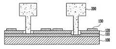
- a gate metal 200obtained by sequentially depositing a Ti layer, a Pt layer, and an Au layer is deposited in the gate regions defined by the first through fourth resist patterns 150 , 160 , 170 , and 180 . Thereafter, a lift-off process is conducted, thereby removing the first through fourth resist patterns 150 , 160 , 170 , and 180 .
- T-shaped gate electrodesare formed such that transistors having different modes or threshold voltages can be manufactured.
- transistors having different threshold voltagesare simultaneously manufactured on a substrate through a lithography process using a multilayered resist layer and a dry etching process using an etch selectivity of the resist layer with respect to an insulating layer.
- transistors having different modes or threshold voltagescan be manufactured on the same substrate without additional mask patterns, with the result that the cost of production can be reduced and the stability and productivity of semiconductor devices can be enhanced.
Landscapes
- Junction Field-Effect Transistors (AREA)
Abstract
Description
- This application claims priority to and the benefit of Korean Patent Application No.2004-100421,filed Dec. 2, 2004, the disclosure of which is incorporated herein by reference in its entirety.
- 1. Field of the Invention
- The present invention relates to a method of manufacturing a field effect transistor (FET) and, more specifically, to a method of manufacturing an FET, in which transistors having respectively different threshold voltages are simultaneously manufactured on a single substrate through a lithography process using a multilayered resist layer and a dry etching process using an etch selectivity of the resist layer with respect to an insulating layer. In this method, the transistors having respectively different threshold voltages can be manufactured without any additional mask pattern, thus reducing the number of processes to be performed and the cost of production.
- 2. Discussion of Related Art
- In general, semiconductor devices, such as a high electron mobility transistor (HEMT) using a compound semiconductor and a metal semiconductor field effect transistor (MESFET), have been manufactured using an ohmic metal layer, which is obtained by sequentially depositing an AuGe layer, a Ni layer, and an Au layer to a predetermined thickness.
- In the manufacture of these semiconductor devices, such as the HEMT using the compound semiconductor and the MESFET, a gate recess process, which is the most important process, is typically performed by measuring currents and includes at least one of a dry process, a wet process, and a combination thereof.
- The gate recess process is performed using BCl3gas or SF6gas in a dry etching system, such as an electron cyclotron resonance (ECR) system or an inductive coupled plasma (ICP) system. Also, the gate recess process may be carried out using a variety of wet etchants, for example, an H3PO4-based solution with a mixture of H3PO4, H2O2, and H2O in an appropriate ratio.
- Further, the manufacture of the semiconductor devices, such as the HEMT using the compound semiconductor and the MESFET, includes forming a gate electrode by sequentially depositing, for example, a Ti layer, a Pt layer, and an Au layer, to a predetermined thickness.
- In the above-described conventional manufacture of the semiconductor devices, when transistors having respectively different threshold voltages are simultaneously formed on a single substrate, separate mask patterns are required. Thus, subsequent processes including a gate recess process should be separately performed.
- For example, given a HEMT device using a compound semiconductor substrate (e.g., a GaAs substrate, an InP substrate, or a GaN substrate), the manufacture of an enhancement mode FET (E-FET) and a depletion mode FET (D-FET) on the same substrate at the same time requires not only separately performing lithography processes using masks or electron-beam (e-beam) lithography processes, but also separately performing subsequent gate recess processes, so that gate recess regions having respectively different etching depths can be obtained.
- Accordingly, when the E-FET and the D-FET are manufactured on the same substrate at the same time, the conventional method leads to an increase in the cost of production with a great number of processes and a drop in productivity.
- The present invention is directed to a method of manufacturing a field effect transistor (FET), in which transistors having respectively different threshold voltages are simultaneously manufactured on a single substrate using a lithography process using a multilayered resist layer and a dry etching process using an etch selectivity of the resist layer with respect to an insulating layer, so that when transistors having different modes or threshold voltages are manufactured on the same substrate, the number of additional lithography processes and their subsequent processes decreases. As a result, the cost of production can be reduced and the stability and productivity of semiconductor devices can be enhanced.
- One aspect of the present invention is to provide a method of manufacturing a FET including steps of: forming an ohmic metal layer on a substrate in source and drain regions; sequentially forming an insulating layer and a multilayered resist layer on the entire surface of the resultant structure and simultaneously forming resist patterns having respectively different shapes in both a first region excluding the ohmic metal layer and a second region excluding the ohmic metal layer, wherein the insulating layer is exposed in the first region, and a lowermost resist pattern is exposed in the second region; exposing the substrate and the insulating layer by simultaneously etching the exposed insulating layer and the exposed lowermost resist pattern using the resist patterns as etch masks, respectively; performing a recess process on the exposed substrate and etching the exposed insulating layer to expose the substrate; and forming gate recess regions having different etching depths from each other over the substrate, depositing a predetermined gate metal, and removing the resist patterns.
- Herein, the step of forming the ohmic metal layer may further include a step of sequentially forming an active layer and a capping layer each having a predetermined thickness between the substrate and the ohmic metal layer.
- Also, the step of forming the ohmic metal layer may include steps of defining the source and drain region using resist patterns; depositing a predetermined ohmic metal; and annealing the ohmic metal using a rapid thermal annealing (RTA) process.
- The thickness of the insulating layer may depend on an etch rate of the multilayered resist layer and the height of a leg portion of a T-shaped gate.
- The above and other features and advantages of the present invention will become more apparent to those of ordinary skill in the art by describing in detail exemplary embodiments thereof with reference to the attached drawings in which:
- FIGS. lA to1I are cross sectional views illustrating a method of manufacturing a field effect transistor (FET) according to an exemplary embodiment of the present invention.
- The present invention will now be described more fully hereinafter with reference to the accompanying drawings, in which exemplary embodiments of the invention are shown. This invention may, however, be embodied in different forms and should not be construed as limited to the embodiments set forth herein. Rather, these embodiments are provided so that this disclosure is thorough and complete and fully conveys the scope of the invention to those skilled in the art.
FIGS. 1A through 1I are cross sectional views illustrating a method of manufacturing a field effect transistor (FET) according to an exemplary embodiment of the present invention.- Referring to
FIG. 1A , anactive layer 110 and acapping layer 120 are sequentially formed on asubstrate 100 to predetermined thicknesses, respectively. Thesubstrate 100 may be any kind of semiconductor substrate and one of a semiconductor substrate such as a Si substrate and a Ge substrate, a compound semiconductor substrate such as a SiGe substrate, a SiC substrate, a GeAs substrate, and an InGaAs substrate, and an insulating substrate such as a glass substrate, a sapphire substrate, a quartz substrate, and a resin substrate. - Referring to
FIG. 1B , a region where source and drain regions (i.e., source and drain ohmic metal layers130) will be formed is defined on thecapping layer 120 using a resist pattern (not shown), and a predetermined ohmic metal is deposited thereon. After that, the resultant structure is annealed using a rapid thermal annealing (RTA) process, thereby forming source and drainohmic metal layers 130 on thecapping layer 120 over thesubstrate 100. - For instance, during the manufacture of a semiconductor device, such as a HEMT using a compound semiconductor or a MESFET, a metal layer, which is obtained by depositing an AuGe layer, a Ni layer, and an Au layer to a predetermined thickness, may be used as the predetermined ohmic metal and annealed using the RTA process so as to form the source and drain
ohmic metal layers 130. - Meanwhile, although it is described in the present embodiment that the source and drain
ohmic metal layers 130 are formed on thecapping layer 120, the present invention is not limited thereto. That is, the source and drainohmic metal layers 130 may be formed directly on thesubstrate 100. Also, theactive layer 110 and thecapping layer 120 may not be formed if required. - Referring to
FIG. 1C , aninsulating layer 140 is deposited on the entire surface of the resultant structure to a predetermined thickness. In this case, theinsulating layer 140 may be formed of, for example, silicon nitride or silicon oxide, and serves to protect the surface of a compound semiconductor substrate. - Also, the thickness of the
insulating layer 140 may be determined considering the etch rate of a resist layer and the height of a leg portion of a T-shaped gate. - Referring to
FIG. 1D , a plurality of resist layers are sequentially coated on theinsulating layer 140 to form a multilayered resist layer. Then, first throughfourth resist patterns - For example, when HEMTs having different modes or threshold voltages are manufactured using an e-beam lithography process, the multilayered resist layer may be a combination of various resists, such as methyl methacrylate and methacrylic acid(co-polymer)/poly methyl methacrylate(PMMA)/co-polymer/PMMA or co-polymer/ZEP/poly-dimethylgutarimide (PMGI)/ZEP.
- The
first resist pattern 150, which is a lowermost pattern, needs to have an appropriate etch rate such that it can be etched together during an etch process of theinsulating layer 140 deposited on thesubstrate 100 to expose thesubstrate 100. In this case, the lowermostfirst resist pattern 150 may be selectively defined in order to obtain the transistors having respectively different modes or threshold voltages. - For instance, when an enhancement mode HEMT (E-HEMT) having a T-shaped gate and a depletion mode HEMT (D-HEMT) having a T-shaped gate are simultaneously manufactured using a multilayered resist layer formed of co-polymer/PMMA/co-polymer/PMMA, an e-beam lithography process is performed such that all the resist patterns including the lowermost first resist pattern150 (i.e., co-polymer) are defined to manufacture the E-HEMT, whereas only other resist patterns excluding the lowermost first resist pattern150 (i.e., co-polymer) are defined to manufacture the D-HEMT.
- Specifically, an exposure process is performed in an appropriate dose and a developing process is performed so that head regions of the T-shaped gates are defined in gate regions of the E-HEMT and the D-HEMT, respectively. Thereafter, an additional exposure process is performed in different doses and an additional developing process is performed so that leg regions of the T-shaped gates are defined to different depths in the gate regions of the E-HEMT and the D-HEMT, respectively.
- In other words, when the leg regions of the T-shaped gates are defined, the resist patterns for the E-HEMT are exposed in a relatively large dose so that even the first resist pattern150 (i.e., co-polymer) can be defined during the developing process. On the other hand, the resist patterns for the D-HEMT are exposed in a relatively small dose so that the first resist pattern150 (i.e., co-polymer) is not defined during the developing process.
- Referring to
FIG. 1E , theinsulating layer 140, which is exposed by the first throughfourth resist patterns opening region 190aover thesubstrate 100 to expose thecapping layer 120. - While the
insulating layer 140 is being dry etched, in the resist patterns for the D-HEMT, the first resist pattern150 (i.e., co-polymer), which is the exposed lowermost pattern, is also etched to the same size as the leg region of the T-shaped gate defined by the second resist pattern160 (i.e., PMMA), thereby forming anopening region 195ain thefirst resist pattern 150 to expose theinsulating layer 140. - In this case, in order to protect the semiconductor surface from plasma after the dry etching process of the
insulating layer 140, a portion of theinsulating layer 140 is dry etched, and the remaining portions thereof are isotropically wet etched using, for example, a buffered oxide etch (BOE) solution. - Also, in the resist patterns for the D-HEMT, the kinds and thicknesses of the lowermost first resist pattern150 (i.e., co-polymer) and the
insulating layer 140 should be selected in consideration of an etch selectivity of thefirst resist pattern 150 with respect to theinsulating layer 140 during the anisotropic dry etching of theinsulating layer 140, such that the lowermostfirst resist pattern 150 is completely etched. - Meanwhile, the anisotropic etching process of the insulating
layer 140 may be performed using CF4gas, a mixture of CF4gas and CHF3gas, or a mixture of CF4gas and O2by means of a reactive ion etching (RIE) system, a magnetically enhanced reactive ion etching (MERIE) system, or an inductive coupled plasma (ICP) system, etc. - Referring to
FIG. 1F , a first recess process is performed on the resist patterns for the E-HEMT. Thus, the exposedcapping layer 120 formed on thesubstrate 100 is etched to a predetermined thickness so that a firstgate recess region 190bis formed in thecapping layer 120. - In this case, because the insulating
layer 140 is exposed by the resist patterns for the D-HEMT over thesubstrate 100, it is not etched during the first recess process. - Referring to
FIG. 1G , the insulatinglayer 140, which is exposed by theopening region 195aformed in the first resistpattern 150, is etched using, for example, a BOE solution or an RIE process. Thus, asecond opening region 195bis formed over thesubstrate 100 such that thecapping layer 120 formed on thesubstrate 100 is exposed also by the resist patterns for the D-HEMT. - During this process, in order to protect the semiconductor surface exposed by the resist patterns for the E-HEMT from plasma, the insulating
layer 140 may be etched using, for example, the BOE solution. - Referring to
FIG. 1H , a second recess process is performed to etch theactive layer 110 and thecapping layer 120 formed on thesubstrate 100. As a result, the first through fourth resistpatterns - In other words, the
capping layer 120 is etched to expose theactive layer 110 in the gate region of one transistor, while theactive layer 110 is etched to a predetermined thickness in the other transistor. - Referring to
FIG. 1I , for example, in order to manufacture HEMTs, agate metal 200 obtained by sequentially depositing a Ti layer, a Pt layer, and an Au layer is deposited in the gate regions defined by the first through fourth resistpatterns patterns - According to the present invention, transistors having different threshold voltages are simultaneously manufactured on a substrate through a lithography process using a multilayered resist layer and a dry etching process using an etch selectivity of the resist layer with respect to an insulating layer. In conclusion, transistors having different modes or threshold voltages can be manufactured on the same substrate without additional mask patterns, with the result that the cost of production can be reduced and the stability and productivity of semiconductor devices can be enhanced.
- Although exemplary embodiments of the present invention have been described with reference to the attached drawings, the present invention is not limited to these embodiments, and it should be appreciated to those skilled in the art that a variety of modifications and changes can be made without departing from the spirit and scope of the present invention.
Claims (12)
Applications Claiming Priority (2)
| Application Number | Priority Date | Filing Date | Title |
|---|---|---|---|
| KR2004-100421 | 2004-12-02 | ||
| KR1020040100421AKR100606290B1 (en) | 2004-12-02 | 2004-12-02 | Manufacturing Method of Field Effect Transistor |
Publications (2)
| Publication Number | Publication Date |
|---|---|
| US20060121658A1true US20060121658A1 (en) | 2006-06-08 |
| US7183149B2 US7183149B2 (en) | 2007-02-27 |
Family
ID=36574847
Family Applications (1)
| Application Number | Title | Priority Date | Filing Date |
|---|---|---|---|
| US11/180,726Expired - LifetimeUS7183149B2 (en) | 2004-12-02 | 2005-07-14 | Method of manufacturing field effect transistor |
Country Status (3)
| Country | Link |
|---|---|
| US (1) | US7183149B2 (en) |
| JP (1) | JP3884047B2 (en) |
| KR (1) | KR100606290B1 (en) |
Cited By (16)
| Publication number | Priority date | Publication date | Assignee | Title |
|---|---|---|---|---|
| US20070228416A1 (en)* | 2005-11-29 | 2007-10-04 | The Hong Kong University Of Science And Technology | Monolithic Integration of Enhancement- and Depletion-mode AlGaN/GaN HFETs |
| US20070278518A1 (en)* | 2005-11-29 | 2007-12-06 | The Hong Kong University Of Science And Technology | Enhancement-Mode III-N Devices, Circuits, and Methods |
| US20070295993A1 (en)* | 2005-11-29 | 2007-12-27 | The Hong Kong University Of Science And Technology | Low Density Drain HEMTs |
| US20090032820A1 (en)* | 2007-08-03 | 2009-02-05 | The Hong Kong University Of Science & Technology | Reliable Normally-Off III-Nitride Active Device Structures, and Related Methods and Systems |
| CN100524634C (en)* | 2007-03-28 | 2009-08-05 | 中国科学院微电子研究所 | A method for preparing transistor T-shaped nano-gate |
| US20100019279A1 (en)* | 2008-04-02 | 2010-01-28 | The Hong Kong University Of Science And Technology | Integrated HEMT and Lateral Field-Effect Rectifier Combinations, Methods, and Systems |
| US20100084687A1 (en)* | 2008-10-03 | 2010-04-08 | The Hong Kong University Of Science And Technology | Aluminum gallium nitride/gallium nitride high electron mobility transistors |
| US20100244043A1 (en)* | 2007-09-12 | 2010-09-30 | Forschungsverbud Berlin E.V. | Electrical devices having improved transfer characteristics and method for tailoring the transfer characteristics of an electrical device |
| US20110034018A1 (en)* | 2007-01-26 | 2011-02-10 | Rfmd (Uk) Limited | Diode assembly |
| US20110057237A1 (en)* | 2009-09-04 | 2011-03-10 | Electronics And Telecommunications Research Institute | Semiconductor devices and methods of forming thereof |
| US20120098599A1 (en)* | 2009-06-30 | 2012-04-26 | Univeristy Of Florida Research Foundation Inc. | Enhancement mode hemt for digital and analog applications |
| US20120315708A1 (en)* | 2011-06-13 | 2012-12-13 | Mitsubishi Electric Corporation | Method for manufacturing semiconductor device |
| US20150129890A1 (en)* | 2012-12-18 | 2015-05-14 | Electronics And Telecommunications Research Institute | Transistor |
| US9281204B2 (en)* | 2014-04-23 | 2016-03-08 | Freescale Semiconductor, Inc. | Method for improving E-beam lithography gate metal profile for enhanced field control |
| US20180026106A1 (en)* | 2016-07-21 | 2018-01-25 | Taiwan Semiconductor Manufacturing Co. Ltd. | Enhancement Mode Field-Effect Transistor with a Gate Dielectric Layer Recessed on a Composite Barrier Layer for High Static Performance |
| CN110808207A (en)* | 2019-11-13 | 2020-02-18 | 中国电子科技集团公司第十三研究所 | T-shaped nano gate and preparation method thereof |
Families Citing this family (12)
| Publication number | Priority date | Publication date | Assignee | Title |
|---|---|---|---|---|
| WO2008062800A1 (en)* | 2006-11-20 | 2008-05-29 | Panasonic Corporation | Semiconductor device and its drive method |
| KR101064726B1 (en)* | 2008-11-24 | 2011-09-14 | 한국전자통신연구원 | Semiconductor device and manufacturing method thereof |
| KR101226955B1 (en) | 2009-12-11 | 2013-01-28 | 한국전자통신연구원 | method for manufacturing Field Effect Transistor |
| RU2463682C1 (en)* | 2011-01-24 | 2012-10-10 | Открытое акционерное общество "Научно-исследовательский институт полупроводниковых приборов" (ОАО "НИИПП") | Method for filed transistor manufacturing |
| JP2013077635A (en)* | 2011-09-29 | 2013-04-25 | Sumitomo Electric Ind Ltd | Semiconductor device and manufacturing method of the same |
| US9502535B2 (en) | 2015-04-10 | 2016-11-22 | Cambridge Electronics, Inc. | Semiconductor structure and etch technique for monolithic integration of III-N transistors |
| US9614069B1 (en) | 2015-04-10 | 2017-04-04 | Cambridge Electronics, Inc. | III-Nitride semiconductors with recess regions and methods of manufacture |
| US9536984B2 (en) | 2015-04-10 | 2017-01-03 | Cambridge Electronics, Inc. | Semiconductor structure with a spacer layer |
| CN108604596A (en) | 2015-07-17 | 2018-09-28 | 剑桥电子有限公司 | Field plate structure for semiconductor device |
| CN111095584B (en) | 2017-08-31 | 2024-07-23 | 谷歌有限责任公司 | Method for manufacturing a device using a multi-layer stack |
| KR102395979B1 (en)* | 2020-09-01 | 2022-05-09 | 포항공과대학교 산학협력단 | Resist mask, domino lithography and structure manufactured using the same |
| KR102356610B1 (en)* | 2020-09-21 | 2022-02-07 | 포항공과대학교 산학협력단 | Resist mask, controlled collapse lithography and structure manufactured using the same |
Citations (2)
| Publication number | Priority date | Publication date | Assignee | Title |
|---|---|---|---|---|
| US6670652B2 (en)* | 2000-10-13 | 2003-12-30 | Kwangju Institute Of Science And Technology | Monolithically integrated E/D mode HEMT and method for fabricating the same |
| US7084021B2 (en)* | 2003-03-14 | 2006-08-01 | Hrl Laboratories, Llc | Method of forming a structure wherein an electrode comprising a refractory metal is deposited |
Family Cites Families (2)
| Publication number | Priority date | Publication date | Assignee | Title |
|---|---|---|---|---|
| KR100276077B1 (en) | 1998-05-11 | 2001-01-15 | 이계철 | Fabrication method of fine T-shaped gate electrode |
| KR100264532B1 (en) | 1998-09-03 | 2000-09-01 | 이계철 | Method for forming fets having their respective mode or threshold voltage |
- 2004
- 2004-12-02KRKR1020040100421Apatent/KR100606290B1/ennot_activeExpired - Fee Related
- 2005
- 2005-07-14USUS11/180,726patent/US7183149B2/ennot_activeExpired - Lifetime
- 2005-07-20JPJP2005210312Apatent/JP3884047B2/ennot_activeExpired - Fee Related
Patent Citations (2)
| Publication number | Priority date | Publication date | Assignee | Title |
|---|---|---|---|---|
| US6670652B2 (en)* | 2000-10-13 | 2003-12-30 | Kwangju Institute Of Science And Technology | Monolithically integrated E/D mode HEMT and method for fabricating the same |
| US7084021B2 (en)* | 2003-03-14 | 2006-08-01 | Hrl Laboratories, Llc | Method of forming a structure wherein an electrode comprising a refractory metal is deposited |
Cited By (26)
| Publication number | Priority date | Publication date | Assignee | Title |
|---|---|---|---|---|
| US7932539B2 (en) | 2005-11-29 | 2011-04-26 | The Hong Kong University Of Science And Technology | Enhancement-mode III-N devices, circuits, and methods |
| US20070278518A1 (en)* | 2005-11-29 | 2007-12-06 | The Hong Kong University Of Science And Technology | Enhancement-Mode III-N Devices, Circuits, and Methods |
| US20070295993A1 (en)* | 2005-11-29 | 2007-12-27 | The Hong Kong University Of Science And Technology | Low Density Drain HEMTs |
| US8044432B2 (en) | 2005-11-29 | 2011-10-25 | The Hong Kong University Of Science And Technology | Low density drain HEMTs |
| US20070228416A1 (en)* | 2005-11-29 | 2007-10-04 | The Hong Kong University Of Science And Technology | Monolithic Integration of Enhancement- and Depletion-mode AlGaN/GaN HFETs |
| US7972915B2 (en)* | 2005-11-29 | 2011-07-05 | The Hong Kong University Of Science And Technology | Monolithic integration of enhancement- and depletion-mode AlGaN/GaN HFETs |
| US8105888B2 (en)* | 2007-01-26 | 2012-01-31 | Rfmd (Uk) Limited | Diode assembly |
| US20110034018A1 (en)* | 2007-01-26 | 2011-02-10 | Rfmd (Uk) Limited | Diode assembly |
| CN100524634C (en)* | 2007-03-28 | 2009-08-05 | 中国科学院微电子研究所 | A method for preparing transistor T-shaped nano-gate |
| US20090032820A1 (en)* | 2007-08-03 | 2009-02-05 | The Hong Kong University Of Science & Technology | Reliable Normally-Off III-Nitride Active Device Structures, and Related Methods and Systems |
| US8502323B2 (en) | 2007-08-03 | 2013-08-06 | The Hong Kong University Of Science And Technology | Reliable normally-off III-nitride active device structures, and related methods and systems |
| US20100244043A1 (en)* | 2007-09-12 | 2010-09-30 | Forschungsverbud Berlin E.V. | Electrical devices having improved transfer characteristics and method for tailoring the transfer characteristics of an electrical device |
| US20100019279A1 (en)* | 2008-04-02 | 2010-01-28 | The Hong Kong University Of Science And Technology | Integrated HEMT and Lateral Field-Effect Rectifier Combinations, Methods, and Systems |
| US8076699B2 (en) | 2008-04-02 | 2011-12-13 | The Hong Kong Univ. Of Science And Technology | Integrated HEMT and lateral field-effect rectifier combinations, methods, and systems |
| US20100084687A1 (en)* | 2008-10-03 | 2010-04-08 | The Hong Kong University Of Science And Technology | Aluminum gallium nitride/gallium nitride high electron mobility transistors |
| US20120098599A1 (en)* | 2009-06-30 | 2012-04-26 | Univeristy Of Florida Research Foundation Inc. | Enhancement mode hemt for digital and analog applications |
| US20110057237A1 (en)* | 2009-09-04 | 2011-03-10 | Electronics And Telecommunications Research Institute | Semiconductor devices and methods of forming thereof |
| US8518794B2 (en)* | 2009-09-04 | 2013-08-27 | Electronics And Telecommunications Research Institute | Semiconductor devices and methods of forming thereof |
| US20120315708A1 (en)* | 2011-06-13 | 2012-12-13 | Mitsubishi Electric Corporation | Method for manufacturing semiconductor device |
| US8778748B2 (en)* | 2011-06-13 | 2014-07-15 | Mitsubishi Electric Corporation | Method for manufacturing semiconductor device |
| US20150129890A1 (en)* | 2012-12-18 | 2015-05-14 | Electronics And Telecommunications Research Institute | Transistor |
| KR101923972B1 (en) | 2012-12-18 | 2018-11-30 | 한국전자통신연구원 | Transistor and Method of Fabricating the Same |
| US9281204B2 (en)* | 2014-04-23 | 2016-03-08 | Freescale Semiconductor, Inc. | Method for improving E-beam lithography gate metal profile for enhanced field control |
| US20180026106A1 (en)* | 2016-07-21 | 2018-01-25 | Taiwan Semiconductor Manufacturing Co. Ltd. | Enhancement Mode Field-Effect Transistor with a Gate Dielectric Layer Recessed on a Composite Barrier Layer for High Static Performance |
| US10068976B2 (en)* | 2016-07-21 | 2018-09-04 | Taiwan Semiconductor Manufacturing Co., Ltd. | Enhancement mode field-effect transistor with a gate dielectric layer recessed on a composite barrier layer for high static performance |
| CN110808207A (en)* | 2019-11-13 | 2020-02-18 | 中国电子科技集团公司第十三研究所 | T-shaped nano gate and preparation method thereof |
Also Published As
| Publication number | Publication date |
|---|---|
| JP2006165507A (en) | 2006-06-22 |
| JP3884047B2 (en) | 2007-02-21 |
| KR100606290B1 (en) | 2006-07-31 |
| KR20060061627A (en) | 2006-06-08 |
| US7183149B2 (en) | 2007-02-27 |
Similar Documents
| Publication | Publication Date | Title |
|---|---|---|
| US7183149B2 (en) | Method of manufacturing field effect transistor | |
| CN100446185C (en) | Method of forming T or gamma shaped electrodes | |
| KR100620393B1 (en) | Field effect transistor and its manufacturing method | |
| JP4143068B2 (en) | Method of manufacturing selectively etched self-aligned double recess high electron mobility transistors | |
| US8586462B2 (en) | Method of manufacturing a field-effect transistor | |
| US7445975B2 (en) | Method for the production of a semiconductor component having a metallic gate electrode disposed in a double-recess structure | |
| US20150194494A1 (en) | Field-effect transistor for high voltage driving and manufacturing method thereof | |
| US20130069127A1 (en) | Field effect transistor and fabrication method thereof | |
| US6153499A (en) | Method of manufacturing semiconductor device | |
| JPH03248439A (en) | Manufacture of compound semiconductor device | |
| US9419083B2 (en) | Semiconductor structures having a gate field plate and methods for forming such structure | |
| JP2004055677A (en) | Gate electrode of field effect transistor and methodof manufacturing the same | |
| KR100264532B1 (en) | Method for forming fets having their respective mode or threshold voltage | |
| KR101875513B1 (en) | Semiconductor device with t-gate of double deck structure and method of fabricating the same | |
| JP2000243758A (en) | Semiconductor device and manufacturing method thereof | |
| KR100849923B1 (en) | Manufacturing Method of Compound Semiconductor Device | |
| KR100582586B1 (en) | Method for manufacturing tee gate of semiconductor device | |
| KR100942698B1 (en) | Manufacturing method of multi-layer metal line | |
| KR20110052336A (en) | Manufacturing method of transistor | |
| US20070066051A1 (en) | Method for forming gate pattern for electronic device | |
| JPH0684951A (en) | Manufacture of semiconductor device | |
| JPH09312299A (en) | Semiconductor device and manufacturing method thereof | |
| JP2000031165A (en) | Method for manufacturing semiconductor device | |
| KR20130037611A (en) | Manufacturing method of field-effect transistor | |
| JPH11121469A (en) | Method for manufacturing field effect transistor |
Legal Events
| Date | Code | Title | Description |
|---|---|---|---|
| AS | Assignment | Owner name:ELECTRONICS AND TELECOMMUNICATIONS RESEARCH INSTIT Free format text:ASSIGNMENT OF ASSIGNORS INTEREST;ASSIGNORS:AHN, HO KYUN;LIM, JONG WON;JI, HONG GU;AND OTHERS;REEL/FRAME:016763/0176 Effective date:20050523 | |
| STCF | Information on status: patent grant | Free format text:PATENTED CASE | |
| FEPP | Fee payment procedure | Free format text:PAYOR NUMBER ASSIGNED (ORIGINAL EVENT CODE: ASPN); ENTITY STATUS OF PATENT OWNER: LARGE ENTITY | |
| AS | Assignment | Owner name:IPG ELECTRONICS 502 LIMITED Free format text:ASSIGNMENT OF ONE HALF (1/2) OF ALL OF ASSIGNORS' RIGHT, TITLE AND INTEREST;ASSIGNOR:ELECTRONICS AND TELECOMMUNICATIONS RESEARCH INSTITUTE;REEL/FRAME:023456/0363 Effective date:20081226 | |
| FPAY | Fee payment | Year of fee payment:4 | |
| FEPP | Fee payment procedure | Free format text:PAT HOLDER NO LONGER CLAIMS SMALL ENTITY STATUS, ENTITY STATUS SET TO UNDISCOUNTED (ORIGINAL EVENT CODE: STOL); ENTITY STATUS OF PATENT OWNER: LARGE ENTITY | |
| AS | Assignment | Owner name:PENDRAGON ELECTRONICS AND TELECOMMUNICATIONS RESEA Free format text:ASSIGNMENT OF ASSIGNORS INTEREST;ASSIGNORS:IPG ELECTRONICS 502 LIMITED;ELECTRONICS AND TELECOMMUNICATIONS RESEARCH INSTITUTE;SIGNING DATES FROM 20120410 TO 20120515;REEL/FRAME:028611/0643 | |
| FEPP | Fee payment procedure | Free format text:PAYER NUMBER DE-ASSIGNED (ORIGINAL EVENT CODE: RMPN); ENTITY STATUS OF PATENT OWNER: LARGE ENTITY | |
| FEPP | Fee payment procedure | Free format text:PAYOR NUMBER ASSIGNED (ORIGINAL EVENT CODE: ASPN); ENTITY STATUS OF PATENT OWNER: LARGE ENTITY | |
| FPAY | Fee payment | Year of fee payment:8 | |
| AS | Assignment | Owner name:UNILOC LUXEMBOURG S.A., LUXEMBOURG Free format text:ASSIGNMENT OF ASSIGNORS INTEREST;ASSIGNOR:PENDRAGON ELECTRONICS AND TELECOMMUNICATIONS RESEARCH LLC;REEL/FRAME:045338/0797 Effective date:20180131 | |
| AS | Assignment | Owner name:UNILOC 2017 LLC, DELAWARE Free format text:ASSIGNMENT OF ASSIGNORS INTEREST;ASSIGNOR:UNILOC LUXEMBOURG S.A.;REEL/FRAME:046532/0088 Effective date:20180503 | |
| FEPP | Fee payment procedure | Free format text:MAINTENANCE FEE REMINDER MAILED (ORIGINAL EVENT CODE: REM.); ENTITY STATUS OF PATENT OWNER: LARGE ENTITY | |
| FEPP | Fee payment procedure | Free format text:11.5 YR SURCHARGE- LATE PMT W/IN 6 MO, LARGE ENTITY (ORIGINAL EVENT CODE: M1556); ENTITY STATUS OF PATENT OWNER: LARGE ENTITY | |
| MAFP | Maintenance fee payment | Free format text:PAYMENT OF MAINTENANCE FEE, 12TH YEAR, LARGE ENTITY (ORIGINAL EVENT CODE: M1553); ENTITY STATUS OF PATENT OWNER: LARGE ENTITY Year of fee payment:12 | |
| AS | Assignment | Owner name:ATREUS LABS LLC, DELAWARE Free format text:ASSIGNMENT OF ASSIGNORS INTEREST;ASSIGNOR:UNILOC 2017 LLC;REEL/FRAME:057453/0790 Effective date:20210727 |