US20060120193A1 - System and method for reducing power consumption during extended refresh periods of dynamic random access memory devices - Google Patents
System and method for reducing power consumption during extended refresh periods of dynamic random access memory devicesDownload PDFInfo
- Publication number
- US20060120193A1 US20060120193A1US11/003,547US354704AUS2006120193A1US 20060120193 A1US20060120193 A1US 20060120193A1US 354704 AUS354704 AUS 354704AUS 2006120193 A1US2006120193 A1US 2006120193A1
- Authority
- US
- United States
- Prior art keywords
- voltage
- refresh
- operable
- cell plate
- array
- Prior art date
- Legal status (The legal status is an assumption and is not a legal conclusion. Google has not performed a legal analysis and makes no representation as to the accuracy of the status listed.)
- Granted
Links
- 238000000034methodMethods0.000titleclaimsdescription10
- 230000015654memoryEffects0.000claimsabstractdescription125
- 230000003068static effectEffects0.000claimsabstractdescription53
- 239000003990capacitorSubstances0.000claimsabstractdescription48
- 230000000295complement effectEffects0.000claimsdescription7
- 230000000737periodic effectEffects0.000claims2
- 230000002829reductive effectEffects0.000abstractdescription16
- 239000000758substrateSubstances0.000abstractdescription10
- 230000009467reductionEffects0.000abstractdescription4
- 238000003491arrayMethods0.000description10
- 238000010586diagramMethods0.000description7
- 230000006870functionEffects0.000description6
- 230000008878couplingEffects0.000description3
- 238000010168coupling processMethods0.000description3
- 238000005859coupling reactionMethods0.000description3
- 238000013459approachMethods0.000description2
- 238000011067equilibrationMethods0.000description2
- 230000014759maintenance of locationEffects0.000description2
- 230000003213activating effectEffects0.000description1
- 238000004364calculation methodMethods0.000description1
- 230000008859changeEffects0.000description1
- 238000013500data storageMethods0.000description1
- 230000003247decreasing effectEffects0.000description1
- 230000000977initiatory effectEffects0.000description1
- 230000000873masking effectEffects0.000description1
- 238000012986modificationMethods0.000description1
- 230000004048modificationEffects0.000description1
- 230000008569processEffects0.000description1
- 230000000717retained effectEffects0.000description1
- 230000001360synchronised effectEffects0.000description1
Images


Classifications
- G—PHYSICS
- G11—INFORMATION STORAGE
- G11C—STATIC STORES
- G11C11/00—Digital stores characterised by the use of particular electric or magnetic storage elements; Storage elements therefor
- G11C11/21—Digital stores characterised by the use of particular electric or magnetic storage elements; Storage elements therefor using electric elements
- G11C11/34—Digital stores characterised by the use of particular electric or magnetic storage elements; Storage elements therefor using electric elements using semiconductor devices
- G11C11/40—Digital stores characterised by the use of particular electric or magnetic storage elements; Storage elements therefor using electric elements using semiconductor devices using transistors
- G11C11/401—Digital stores characterised by the use of particular electric or magnetic storage elements; Storage elements therefor using electric elements using semiconductor devices using transistors forming cells needing refreshing or charge regeneration, i.e. dynamic cells
- G11C11/406—Management or control of the refreshing or charge-regeneration cycles
- G11C11/40615—Internal triggering or timing of refresh, e.g. hidden refresh, self refresh, pseudo-SRAMs
- G—PHYSICS
- G11—INFORMATION STORAGE
- G11C—STATIC STORES
- G11C11/00—Digital stores characterised by the use of particular electric or magnetic storage elements; Storage elements therefor
- G11C11/21—Digital stores characterised by the use of particular electric or magnetic storage elements; Storage elements therefor using electric elements
- G11C11/34—Digital stores characterised by the use of particular electric or magnetic storage elements; Storage elements therefor using electric elements using semiconductor devices
- G11C11/40—Digital stores characterised by the use of particular electric or magnetic storage elements; Storage elements therefor using electric elements using semiconductor devices using transistors
- G11C11/401—Digital stores characterised by the use of particular electric or magnetic storage elements; Storage elements therefor using electric elements using semiconductor devices using transistors forming cells needing refreshing or charge regeneration, i.e. dynamic cells
- G11C11/4063—Auxiliary circuits, e.g. for addressing, decoding, driving, writing, sensing or timing
- G11C11/407—Auxiliary circuits, e.g. for addressing, decoding, driving, writing, sensing or timing for memory cells of the field-effect type
- G11C11/4074—Power supply or voltage generation circuits, e.g. bias voltage generators, substrate voltage generators, back-up power, power control circuits
- G—PHYSICS
- G11—INFORMATION STORAGE
- G11C—STATIC STORES
- G11C11/00—Digital stores characterised by the use of particular electric or magnetic storage elements; Storage elements therefor
- G11C11/21—Digital stores characterised by the use of particular electric or magnetic storage elements; Storage elements therefor using electric elements
- G11C11/34—Digital stores characterised by the use of particular electric or magnetic storage elements; Storage elements therefor using electric elements using semiconductor devices
- G11C11/40—Digital stores characterised by the use of particular electric or magnetic storage elements; Storage elements therefor using electric elements using semiconductor devices using transistors
- G11C11/401—Digital stores characterised by the use of particular electric or magnetic storage elements; Storage elements therefor using electric elements using semiconductor devices using transistors forming cells needing refreshing or charge regeneration, i.e. dynamic cells
- G11C11/4063—Auxiliary circuits, e.g. for addressing, decoding, driving, writing, sensing or timing
- G11C11/407—Auxiliary circuits, e.g. for addressing, decoding, driving, writing, sensing or timing for memory cells of the field-effect type
- G11C11/409—Read-write [R-W] circuits
- G11C11/4096—Input/output [I/O] data management or control circuits, e.g. reading or writing circuits, I/O drivers or bit-line switches
- G—PHYSICS
- G11—INFORMATION STORAGE
- G11C—STATIC STORES
- G11C2211/00—Indexing scheme relating to digital stores characterized by the use of particular electric or magnetic storage elements; Storage elements therefor
- G11C2211/401—Indexing scheme relating to cells needing refreshing or charge regeneration, i.e. dynamic cells
- G11C2211/406—Refreshing of dynamic cells
- G11C2211/4067—Refresh in standby or low power modes
- G—PHYSICS
- G11—INFORMATION STORAGE
- G11C—STATIC STORES
- G11C2211/00—Indexing scheme relating to digital stores characterized by the use of particular electric or magnetic storage elements; Storage elements therefor
- G11C2211/401—Indexing scheme relating to cells needing refreshing or charge regeneration, i.e. dynamic cells
- G11C2211/406—Refreshing of dynamic cells
- G11C2211/4068—Voltage or leakage in refresh operations
- G—PHYSICS
- G11—INFORMATION STORAGE
- G11C—STATIC STORES
- G11C7/00—Arrangements for writing information into, or reading information out from, a digital store
- G11C7/10—Input/output [I/O] data interface arrangements, e.g. I/O data control circuits, I/O data buffers
- G11C7/1006—Data managing, e.g. manipulating data before writing or reading out, data bus switches or control circuits therefor
- G—PHYSICS
- G11—INFORMATION STORAGE
- G11C—STATIC STORES
- G11C7/00—Arrangements for writing information into, or reading information out from, a digital store
- G11C7/10—Input/output [I/O] data interface arrangements, e.g. I/O data control circuits, I/O data buffers
- G11C7/1078—Data input circuits, e.g. write amplifiers, data input buffers, data input registers, data input level conversion circuits
Definitions
- This inventionrelates to dynamic random access memory devices, and, more particularly, to a system and method for reducing memory cell leakage during extended refresh periods to allow the time between refreshes to be increase, thereby reducing power consumption.
- Many battery-powered portable electronic devicessuch as laptop computers, Portable Digital Assistants, cell phones, and the like, require memory devices that provide large storage capacity and low power consumption.
- the devicestypically operate in a low-power mode when the device is not being used.
- a supply voltage or voltages applied to electronic componentssuch as a microprocessor, associated control chips, and memory devices are typically reduced to lower the power consumption of the components, as will be appreciated by those skilled in the art.
- the supply voltagesare varied to reduce power consumption in the low-power mode, data stored in the electronic components such as the memory devices must be retained.
- DRAMdynamic random access memory
- SRAMstatic random access memory
- FLASH memory devicesnon-volatile memories
- DRAM deviceshave the disadvantage that their memory cells must be continually refreshed because of the means by which they store data. Refreshing DRAM memory cells tends to consume power at a substantial rate.
- DRAM memory cellseach consists of a capacitor that is charged to one of two voltages to store a bit of data. Charge leaks from the capacitor by various means. It is for this reason that DRAM memory cells must be refreshed by recharging them to the original voltage.
- Refreshis typically performed by essentially reading data bits from the memory cells in each row of a memory cell array and then writing those same data bits back to the same cells in the row. This refresh is generally performed on a row-by-row basis at a rate needed to keep charge stored in the memory cells from leaking excessively between refreshes.
- a row of memory cellsis refreshed, a pair of digit lines for each memory cell are switched to complementary voltages and then equilibrated, which consumes a significant amount power. As the number of columns in the memory cell array increases with increasing memory capacity, the power consumed in actuating each row increases accordingly.
- the amount of power consumed by refreshalso depends on which of several refresh modes is active.
- a Self Refresh modeis normally active during periods when data are not being read from or written to the DRAM device. Since portable electronic devices are often inactive for substantial periods of time, the amount of power consumed during Self Refresh can be an important factor in determining how long the electronic device can be used between battery charges.
- the amount of power consumed by refreshing DRAM devices in any refresh modeis proportional to the rate at which it is necessary to perform refreshes. If the required refresh rate for a DRAM device could be reduced, so also could the refresh power consumption.
- the required refresh rateis determined by the rate at which charge leaks from the memory cell capacitors. Therefore, some attempts to increase the time required between refreshes have focused on adjusting the rate of refresh as a function of the rate of charge leakage from memory cell capacitors. For example, since the rate at which charge leaks from memory cells capacitors is a function of temperature, some power saving techniques adjust the refresh rate as a function of temperature. As a result, refreshes do not occur more frequently than necessary.
- a portion of a typical DRAM array 100includes a plurality of memory cells 110 , each of which is coupled to a word line WL and a digit line DL.
- the memory cells 110 in the array 100are arranged in rows and columns, with a word line being provided for each row of memory cells 100 .
- the word lines WLare coupled to and actuated by a row decoder 112 responsive to a row address A 0 -AX.
- the DRAM array 100has a folded digit line architecture so that complimentary digit lines DL and DL* are provided for each column of memory cells 110 .
- a single digit line DLis included in the array for each column of memory cells 110 .
- the other digit lineis provided by an adjacent array.
- each memory cell 110includes a memory cell capacitor 114 coupled between a cell plate 116 and a storage node 118 .
- the cell plateis normally common to all of the memory cells 110 in an array, and it is generally biased to a voltage of V CC /2.
- An access transistor 120is coupled between the storage node 118 and a digit line DL for the column containing the memory cell 110 .
- the gate of the access transistor 120is coupled to a word line WL for the row containing the memory cell 110 .
- a voltage corresponding to the data bitis applied to the digit line DL to which the memory cell 110 is coupled, and the voltage applied to the word line WL is driven high to turn ON the access transistor 120 .
- the access transistorthen couples the digit line DL to the capacitor 114 to store the voltage of the digit line DL in the capacitor 114 .
- the digit line DLis first equilibrated to an equilibration voltage, generally to V CC /2, and the word line WL is then driven high to turn ON the access transistor 120 .
- the access transistor 120then couples the capacitor 114 to the digit line DL to slightly alter the voltage on the digit line DL above or below the equilibration voltage depending upon the voltage stored in the capacitor 114 .
- An n-sense amplifier 130 and a p-sense amplifier 132sense whether the voltage has increased or decreased responsive to applying an active low NSENSE* signal of normally zero volts to the n-sense amplifier 130 and applying an active high PSENSE signal of normally V CC to the p-sense amplifier 132 .
- the NSENSE* signal and the PSENSE signalare supplied by control circuitry (not shown) in a DRAM.
- a column decoder 136couples one of the pairs of complimentary digit lines DL, DL* to complimentary input/output lines “IO, IO* responsive to a column address A 0 -AY.
- the above-described memory read process of activating a word line WL and then sensing the digit line voltage of all memory cells 100 in the row for the active word line WLis what is done to refresh the memory cells 100 . If the voltage on the capacitor 114 has been excessively discharged from V CC or excessively charged from zero volts between refreshes, it can be impossible for the sense amplifiers 130 , 132 to accurately read the voltage to which the memory cell capacitor 114 was charged. The result is an erroneous reading of the memory cell 100 known as a data retention error.
- the charge placed on a memory cell capacitor 114dissipates through a variety of paths.
- One discharge pathis through the dielectric of the capacitor 114 itself.
- Another significant discharge pathis through the access transistors 120 coupling the capacitors 114 to the digit lines DL when the transistors 120 are turned OFF.
- This leakage currentis known as the “sub-threshold” leakage current of the transistors 120 . Reducing the sub-threshold leakage current of the access transistors 120 allows the capacitor 114 s to retain a voltage that is close enough to the voltage initially placed on the capacitors 114 for a data retention error to be avoided.
- a typical memory cell access transistor 120is in NMOS transistor for up in a P-type substrate 140 having a first n-doped source/drain region 142 and a second n-doped source/drain region 144 .
- the first n-doped source/drain region 142is coupled to a digit line DL
- the second n-doped source/drain region 144is coupled to a memory cell capacitor 114 .
- the access transistor 120also includes a gate formed by a gate electrode 146 insulated from the substrate 140 by an oxide layer 148 .
- the gate electrode 146is coupled to a word line WL.
- the n-doped source/drain region 144 that is coupled to the memory cell capacitor and the p-doped substrate 140together form a diode junction 150 , which is schematically illustrated in FIG. 3 along with the access transistor 120 and the memory cell capacitor 114 .
- the substrate 140is biased to a voltage V DD that is typically negative, such as ⁇ 0.5 V.
- the cell plate 116is typically biased to V CC /2, such as 1 V, as shown in FIG. 3 . Therefore, when the memory cell capacitor 114 is charged to a voltage of V CC , which in this example is 2 V, the diode junction 150 is back-biased with a voltage of 2.5 V.
- a system and method of refreshing memory cells in an arrayallows refresh to occur in a normal refresh mode or in a static refresh mode, such as a self-refresh mode.
- a cell plate for the arrayis biased to a first voltage, such as one-half a supply voltage.
- the cell plateis also biased to the first voltage in the static refresh mode when the memory cells are being refreshed, which preferably occurs in a burst manner.
- the cell plateis biased to a second voltage in the static refresh mode when the memory cells are not being refreshed. This second voltage reduces the voltage between the source/drain of access transistors for the memory cells and the substrate, thereby reducing leakage current from memory cell capacitors. As a result, a reduced refresh rate can be achieved.
- FIG. 1is a schematic diagram showing a portion of a typical DRAM memory cell array.
- FIG. 2is a cross-sectional view filed a typical access transistor used in the memory cell array of FIG. 1 .
- FIG. 3is a schematic diagram showing a diode junction formed by the access transistor of FIG. 2 .
- FIG. 4is a schematic diagram showing memory cell of FIG. 3 in which the memory cell capacitor has been charged to V CC .
- FIG. 5is a schematic diagram showing memory cell of FIG. 3 in which the memory cell capacitor has been charged to 0V.
- FIG. 6is a block diagram of a DRAM device according to one embodiment of the invention.
- FIG. 7is a block diagram showing a cell plate voltage selector used in the DRAM device of FIG. 6 .
- FIG. 8is a truth table showing the operation of the cell plate voltage selector of FIG. 7 .
- FIG. 9is a block diagram of a processor-based system using the DRAM device of FIG. 6 .
- the memory cell 110 shown in FIG. 4contains the access transistor 120 , the memory cell capacitor 114 and the diode junction 150 .
- the memory cell capacitor 114is initially charged to V CC , which is, in this example, 2 V. As previously explained, this condition places 2.5 V across the diode junction 150 is it results in substantial leakage from the memory cell capacitor 114 .
- V CCwhich is, in this example, 2 V.
- the DRAMreduces the bias voltage on the cell plate 116 from V CC /2 to a lesser voltage V CC /2 ⁇ V, which, in this example, is a change in voltage from 1V to 0.5V.
- V CC /2 ⁇ Va voltage on the cell plate 116
- V CC /2 ⁇ Va voltage on the other plate 118 of the memory cell capacitor 114
- ⁇ Vthe voltage on the other plate 118 of the memory cell capacitor 114
- the voltage across the diode junction 150is therefore reduced from 2.5 V to 2.0 V. Even this relatively small reduction in the voltage across the diode junction 150 can significantly reduce the rate at which charge leaks from the memory cell capacitor 114 , thereby allowing a reduction in the required refresh rate.
- the cell plate voltageis preferably reduced only during self-refresh and any other static refresh mode in which data are not been read from or written to the DRAM device for a considerable period. Furthermore, refreshes during this period should occur in a burst mode in which the entire DRAM array is refreshed in rapid sequence rather than in a distributed mode in which portions of the DRAM array are continuously being refreshed. By using a burst refresh mode, a considerable time will exist between refreshes, during which the cell plate voltage can be reduced from V CC to V CC ⁇ V, thereby saving considerable power even with the expenditure of power incurred in reducing the cell plate voltage.
- the required refresh ratecould be reduced even further by reducing the cell plate voltage even further, the reasons for not doing so will be explained using the example shown in FIG. 5 in which the memory cell capacitor 114 has been initially charged to 0 V. Therefore, when the voltage on the cell plate 116 is reduced from 1V. to 0.5V, the voltage on the other plate 118 of the memory cell capacitor 114 is reduced to ⁇ 0.5V. The voltage across the diode junction 150 is therefore reduced from 0.5V to 0V. However, if the voltage of the cell plate 116 was reduced to a greater extent, the voltage on the plate 118 of the memory cell capacitor 114 would become even more negative, and might forward-bias the diode junction 150 .
- the diode junction 150became forward-biased, the current leakage would be extraordinarily higher. Forward biasing the diode junction 150 could be prevented by making the substrate voltage VDD even more negative, but doing so would consume substantial power, might interfere with the operation of other portions of the DRAM device, and, by increasing the voltage differential between the store voltage in the substrate as well as other differentials, might increase charge leakage in other respects.
- the need to prevent the diode junction 150 from becoming forward-biasedtherefore limits the extent to which the cell plate voltage can be reduced in a static refresh mode.
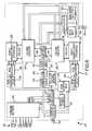
- a synchronous DRAM (“SDRAM”) device 200in the shown in FIG. 6 .
- the SDRAM 200includes a command decoder 204 that controls the operation of the SDRAM 200 responsive to high-level command signals received on a control bus 206 .
- These high level command signalswhich are typically generated by a memory controller (not shown in FIG. 6 ), are a clock enable signal CKE*, a clock signal CLK, a chip select signal CS*, a write enable signal WE*, a row address strobe signal RAS*, a column address strobe signal CAS*, and a data mask signal DQM, in which the “*” designates the signal as active low.
- the command decoder 204generates a sequence of command signals responsive to the high level command signals to carry out the function (e.g., a read or a write) designated by each of the high level command signals. For example, the command decoder 204 can receive and decode a command to cause the SDRAM to enter a self-refresh mode when the SDRAM is expected to not be active for a period.
- These command signals, and the manner in which they accomplish their respective functions,are conventional. Therefore, in the interest of brevity, a further explanation of these command signals will be omitted.
- the SDRAM 200includes an address register 212 that receives row addresses and column addresses through an address bus 214 .
- the address bus 214is generally applied to a memory controller (not shown in FIG. 6 ).
- a row addressis generally first received by the address register 212 and applied to a row address multiplexer 218 .
- the row address multiplexer 218couples the row address to a number of components associated with either of two memory banks 220 , 222 depending upon the state of a bank address bit forming part of the row address.
- Associated with each of the memory banks 220 , 222is a respective row address latch 226 , which stores the row address, and a row decoder 228 , which decodes the row address and applies corresponding signals to one of the arrays 220 or 222 .
- the row address multiplexer 218also couples row addresses to the row address latches 226 for the purpose of refreshing the memory cells in the arrays 220 , 222 .
- the row addressesare generated for refresh purposes by a refresh counter 230 , which is controlled by a refresh controller 232 .
- the refresh controller 232is, in turn, controlled by the command decoder 204 .
- the refresh controller 232is coupled to a cell plate voltage selector 234 . More specifically, the cell plate voltage selector 234 receives complimentary control signals C, C* that cause the circuit selector to apply either a normal bias voltage V N or a static refresh bias voltage V R to the cell plates in the respective memory banks 220 , 222 .
- the normal bias voltage V Nis 1V
- the static refresh bias voltage V Ris 0.5V.
- the refresh controller 232when entering a static refresh mode, such as a self-refresh mode, applies control signals C, C* to the cell plate voltage selector 234 that cause it to discontinue coupling the voltage V N to the cell plates in the memory banks 220 , 222 and instead couple the voltage V R to the cell plates.
- the refresh controller 232Prior to initiating a refresh of any of the rows of memory cells in the banks 220 , 222 , the refresh controller 232 applies control signals C, C* to the cell plate voltage selector 234 to cause it to coupling the normal bias voltage V N to the cell plates.
- the refresh controller 232then initiates a burst refresh of all of the memory cells in the memory banks 220 , 222 .
- the refresh controller 232then causes the cell plate voltage selector 234 to again couple the static refresh bias voltage V R to the cell plates in the memory banks 220 , 222 .
- the refresh controller 232applies control signals C, C* to the cell plate voltage selector 234 that causes it to apply the normal bias voltage V N to the cell plates of the memory banks 220 , 222 .
- a column addressis applied to the address register 212 .
- the address register 212couples the column address to a column address latch 240 .
- the column addressis either coupled through a burst counter 242 to a column address buffer 244 , or to the burst counter 242 which applies a sequence of column addresses to the column address buffer 244 starting at the column address output by the address register 212 .
- the column address buffer 244applies a column address to a column decoder 248 .
- Data to be read from one of the arrays 220 , 222is coupled to the column circuitry 254 , 255 for one of the arrays 220 , 222 , respectively.
- the datais then coupled through a data output register 256 to a data bus 258 .
- Data to be written to one of the arrays 220 , 222are coupled from the data bus 258 to a data input register 260 .
- the write dataare coupled to the column circuitry 254 , 255 where they are transferred to one of the arrays 220 , 222 , respectively.
- a mask register 264responds to a data mask DM signal to selectively alter the flow of data into and out of the column circuitry 254 , 255 , such as by selectively masking data to be read from the arrays 220 , 222 .
- FIG. 7One embodiment of a cell plate voltage selector 270 that can be used as the cell plate voltage selector circuit 234 in the SDRAM 200 of FIG. 6 is shown in FIG. 7 .
- the cell plate voltage selector 270includes a pair of pass gates 272 , 275 that are controlled by the control signals C, C* in a manner that causes the pass gates to be alternately enabled.
- the pass gate 272is coupled to receive a normal voltage V N of V CC /2 while the pass gate 274 is coupled to receive a static refresh bias voltage V R of V CC /4.
- V CCis equal to 2 volts, so V CC /2 is equal to 1V, and V CC /4 is equal to 0.5V.
- other voltagescan be used. In either case, these voltages are provided by conventional means.
- the pass gates 272 , 274alternately couple either V CC /2 or V CC /4 to a differential amplifier 280 configured to operate as a voltage follower.
- the output of the amplifier 280is coupled to a cell plate 290 .
- the amplifier 280 configured as a voltage followerapplies a voltage to its output that is equal to the voltage applied to its non-inverting input (“+”).
- the amplifier 280has sufficient current drive to quickly drive the cell plate 290 to either V CC /2 or V CC /4, depending on what pass gate 272 , 274 is conductive.
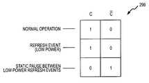
- the operation of the cell plate voltage selector 270is summarized by the truth table 296 shown in FIG. 8 .
- the refresh controller 232( FIG. 6 ) outputs control signals C,C* of “1,0” to make the pass gate 272 conductive and to make the pass gate 274 non-conductive.
- the differential amplifier 280then receives and applies to the cell plate 290 the normal bias voltage V N of V CC /2.
- the refresh controller 232outputs control signals C,C* of “0,1” to make the pass gate 272 non-conductive and the pass gate 274 conductive.
- the differential amplifier 280then receives and applies to the cell plate 290 the static refresh bias voltage V R of V CC /4.
- the SDRAM 200 shown in FIG. 6can be used in various electronic systems. For example, it may be used in a processor-based system, such as a computer system 300 shown in FIG. 9 .
- the computer system 300includes a processor 302 for performing various computing functions, such as executing specific software to perform specific calculations or tasks.
- the processor 302includes a processor bus 304 that normally includes an address bus, a control bus, and a data bus.
- the computer system 300includes one or more input devices 314 , such as a keyboard or a mouse, coupled to the processor 302 to allow an operator to interface with the computer system 300 .
- the computer system 300also includes one or more output devices 316 coupled to the processor 302 , such output devices typically being a printer or a video terminal.
- One or more data storage devices 318are also typically coupled to the processor 302 to allow the processor 302 to store data in or retrieve data from internal or external storage media (not shown). Examples of typical storage devices 318 include hard and floppy disks, tape cassettes, and compact disk read-only memories (CD-ROMs).
- the processor 302is also typically coupled to cache memory 326 , which is usually static random access memory (“SRAM”), and to the SDRAM 200 through a memory controller 330 .
- the memory controller 330normally includes a control bus 336 and an address bus 338 that are coupled to the SDRAM 200 .
- a data bus 340is coupled from the SDRAM 200 to the processor bus 304 either directly (as shown), through the memory controller 330 , or by some other means.
Landscapes
- Engineering & Computer Science (AREA)
- Microelectronics & Electronic Packaging (AREA)
- Computer Hardware Design (AREA)
- Dram (AREA)
Abstract
Description
- This invention relates to dynamic random access memory devices, and, more particularly, to a system and method for reducing memory cell leakage during extended refresh periods to allow the time between refreshes to be increase, thereby reducing power consumption.
- Many battery-powered portable electronic devices, such as laptop computers, Portable Digital Assistants, cell phones, and the like, require memory devices that provide large storage capacity and low power consumption. To reduce the power consumption and thereby extend the operating time of such devices between recharges, the devices typically operate in a low-power mode when the device is not being used. In the low-power mode, a supply voltage or voltages applied to electronic components such as a microprocessor, associated control chips, and memory devices are typically reduced to lower the power consumption of the components, as will be appreciated by those skilled in the art. Although the supply voltages are varied to reduce power consumption in the low-power mode, data stored in the electronic components such as the memory devices must be retained.
- A large storage capacity is typically desired in these devices to maximize the amount of available storage. For this reasons, it is usually desirable to utilize dynamic random access memory (“DRAM”) devices, which have a relatively large storage capacity, over other types of memories such as static random access memory (“SRAM”) devices and non-volatile memories such as FLASH memory devices. However, DRAM devices have the disadvantage that their memory cells must be continually refreshed because of the means by which they store data. Refreshing DRAM memory cells tends to consume power at a substantial rate. As is well-known in the art, DRAM memory cells each consists of a capacitor that is charged to one of two voltages to store a bit of data. Charge leaks from the capacitor by various means. It is for this reason that DRAM memory cells must be refreshed by recharging them to the original voltage. Refresh is typically performed by essentially reading data bits from the memory cells in each row of a memory cell array and then writing those same data bits back to the same cells in the row. This refresh is generally performed on a row-by-row basis at a rate needed to keep charge stored in the memory cells from leaking excessively between refreshes. Each time a row of memory cells is refreshed, a pair of digit lines for each memory cell are switched to complementary voltages and then equilibrated, which consumes a significant amount power. As the number of columns in the memory cell array increases with increasing memory capacity, the power consumed in actuating each row increases accordingly.
- The amount of power consumed by refresh also depends on which of several refresh modes is active. A Self Refresh mode is normally active during periods when data are not being read from or written to the DRAM device. Since portable electronic devices are often inactive for substantial periods of time, the amount of power consumed during Self Refresh can be an important factor in determining how long the electronic device can be used between battery charges.
- The amount of power consumed by refreshing DRAM devices in any refresh mode is proportional to the rate at which it is necessary to perform refreshes. If the required refresh rate for a DRAM device could be reduced, so also could the refresh power consumption. The required refresh rate is determined by the rate at which charge leaks from the memory cell capacitors. Therefore, some attempts to increase the time required between refreshes have focused on adjusting the rate of refresh as a function of the rate of charge leakage from memory cell capacitors. For example, since the rate at which charge leaks from memory cells capacitors is a function of temperature, some power saving techniques adjust the refresh rate as a function of temperature. As a result, refreshes do not occur more frequently than necessary.
- Other attempts to increase the time required between refreshes have focused on reducing the amount of charge leakage from memory cell capacitors. With reference to
FIG. 1 , a portion of atypical DRAM array 100 includes a plurality ofmemory cells 110, each of which is coupled to a word line WL and a digit line DL. Thememory cells 110 in thearray 100 are arranged in rows and columns, with a word line being provided for each row ofmemory cells 100. The word lines WL are coupled to and actuated by arow decoder 112 responsive to a row address A0-AX. As shown inFIG. 1 , theDRAM array 100 has a folded digit line architecture so that complimentary digit lines DL and DL* are provided for each column ofmemory cells 110. In a memory array having an open digit line architecture (not shown), a single digit line DL is included in the array for each column ofmemory cells 110. The other digit line is provided by an adjacent array. However, the following discussion of the problems with DRAM arrays and prior attempts to solve such problems is applicable to arrays having an open digit line architecture as well as arrays having a folded digit line architecture. - Regardless of whether the array has a folded digit line architecture or an open digit line architecture, each
memory cell 110 includes amemory cell capacitor 114 coupled between acell plate 116 and astorage node 118. The cell plate is normally common to all of thememory cells 110 in an array, and it is generally biased to a voltage of VCC/2. Anaccess transistor 120 is coupled between thestorage node 118 and a digit line DL for the column containing thememory cell 110. The gate of theaccess transistor 120 is coupled to a word line WL for the row containing thememory cell 110. When a data bit is to be written to thememory cell 110, a voltage corresponding to the data bit, generally either VCCor zero volts, is applied to the digit line DL to which thememory cell 110 is coupled, and the voltage applied to the word line WL is driven high to turn ON theaccess transistor 120. The access transistor then couples the digit line DL to thecapacitor 114 to store the voltage of the digit line DL in thecapacitor 114. For a read operation, the digit line DL is first equilibrated to an equilibration voltage, generally to VCC/2, and the word line WL is then driven high to turn ON theaccess transistor 120. Theaccess transistor 120 then couples thecapacitor 114 to the digit line DL to slightly alter the voltage on the digit line DL above or below the equilibration voltage depending upon the voltage stored in thecapacitor 114. An n-sense amplifier 130 and a p-sense amplifier 132 sense whether the voltage has increased or decreased responsive to applying an active low NSENSE* signal of normally zero volts to the n-sense amplifier 130 and applying an active high PSENSE signal of normally VCCto the p-sense amplifier 132. The NSENSE* signal and the PSENSE signal are supplied by control circuitry (not shown) in a DRAM. If a voltage increase was sensed, the p-sense amplifier 132 drives the digit line DL to VCC, and, if a voltage decrease was sensed, the n-sense amplifier 130 drives the digit line DL to zero volts. The voltage applied to the digit line DL by thesense amplifiers capacitor 114 to the voltage to which it was originally charged. Acolumn decoder 136 couples one of the pairs of complimentary digit lines DL, DL* to complimentary input/output lines “IO, IO* responsive to a column address A0-AY. - The above-described memory read process of activating a word line WL and then sensing the digit line voltage of all
memory cells 100 in the row for the active word line WL is what is done to refresh thememory cells 100. If the voltage on thecapacitor 114 has been excessively discharged from VCCor excessively charged from zero volts between refreshes, it can be impossible for thesense amplifiers memory cell capacitor 114 was charged. The result is an erroneous reading of thememory cell 100 known as a data retention error. - As is well known in the art, the charge placed on a
memory cell capacitor 114 dissipates through a variety of paths. One discharge path is through the dielectric of thecapacitor 114 itself. Another significant discharge path is through theaccess transistors 120 coupling thecapacitors 114 to the digit lines DL when thetransistors 120 are turned OFF. This leakage current is known as the “sub-threshold” leakage current of thetransistors 120. Reducing the sub-threshold leakage current of theaccess transistors 120 allows the capacitor114sto retain a voltage that is close enough to the voltage initially placed on thecapacitors 114 for a data retention error to be avoided. Various approaches have been used to reduce the sub-threshold leakage of theaccess transistors 120 to allowmemory cell capacitors 114 to retain charge for a longer period between refreshes. Some of these approaches rely on increasing the threshold voltage VT of theaccess transistor 120 by either biasing the word lines to a negative voltage when the word line is not active or by biasing the substrate to a less negative voltage. - Another path through with the charge placed on a
memory cell capacitor 114 can dissipates is from theaccess transistor 120 to the substrate. With reference toFIG. 2 , a typical memorycell access transistor 120 is in NMOS transistor for up in a P-type substrate 140 having a first n-doped source/drain region 142 and a second n-doped source/drain region 144. The first n-doped source/drain region 142 is coupled to a digit line DL, and the second n-doped source/drain region 144 is coupled to amemory cell capacitor 114. Theaccess transistor 120 also includes a gate formed by agate electrode 146 insulated from thesubstrate 140 by anoxide layer 148. Thegate electrode 146 is coupled to a word line WL. The n-doped source/drain region 144 that is coupled to the memory cell capacitor and the p-dopedsubstrate 140 together form adiode junction 150, which is schematically illustrated inFIG. 3 along with theaccess transistor 120 and thememory cell capacitor 114. Thesubstrate 140 is biased to a voltage VDDthat is typically negative, such as −0.5 V. As previously mentioned, thecell plate 116 is typically biased to VCC/2, such as 1 V, as shown inFIG. 3 . Therefore, when thememory cell capacitor 114 is charged to a voltage of VCC, which in this example is 2 V, thediode junction 150 is back-biased with a voltage of 2.5 V. Unfortunately, even though thediode junction 150 is back-biased, a significant amount of charge leaks through thediode junction 150. This charge leakage limits the period of time that thememory cell capacitor 114 can retain its charge without being refreshed. As a result, thememory cell capacitor 114 must be frequently refreshed, thereby causing a DRAM device containing thememory cell capacitor 114 to consume substantial power. - There is therefore a need for a technique to reduce the charge leakage through the
diode junction 150 so that the time between required refreshes can be increased, thereby allowing DRAM devices to consume less power. - A system and method of refreshing memory cells in an array allows refresh to occur in a normal refresh mode or in a static refresh mode, such as a self-refresh mode. In the normal refresh mode, a cell plate for the array is biased to a first voltage, such as one-half a supply voltage. The cell plate is also biased to the first voltage in the static refresh mode when the memory cells are being refreshed, which preferably occurs in a burst manner. However, the cell plate is biased to a second voltage in the static refresh mode when the memory cells are not being refreshed. This second voltage reduces the voltage between the source/drain of access transistors for the memory cells and the substrate, thereby reducing leakage current from memory cell capacitors. As a result, a reduced refresh rate can be achieved.
FIG. 1 is a schematic diagram showing a portion of a typical DRAM memory cell array.FIG. 2 is a cross-sectional view filed a typical access transistor used in the memory cell array ofFIG. 1 .FIG. 3 is a schematic diagram showing a diode junction formed by the access transistor ofFIG. 2 .FIG. 4 is a schematic diagram showing memory cell ofFIG. 3 in which the memory cell capacitor has been charged to VCC.FIG. 5 is a schematic diagram showing memory cell ofFIG. 3 in which the memory cell capacitor has been charged to 0V.FIG. 6 is a block diagram of a DRAM device according to one embodiment of the invention.FIG. 7 is a block diagram showing a cell plate voltage selector used in the DRAM device ofFIG. 6 .FIG. 8 is a truth table showing the operation of the cell plate voltage selector ofFIG. 7 .FIG. 9 is a block diagram of a processor-based system using the DRAM device ofFIG. 6 .- The principal of the operation of one embodiment of the invention is exemplified by the
memory cell 110 shown inFIG. 4 , which contains theaccess transistor 120, thememory cell capacitor 114 and thediode junction 150. As shown inFIG. 4 , thememory cell capacitor 114 is initially charged to VCC, which is, in this example, 2 V. As previously explained, this condition places 2.5 V across thediode junction 150 is it results in substantial leakage from thememory cell capacitor 114. According to one embodiment of the invention, when a DRAM containing thememory cell 110 shown inFIG. 4 is to operate in a self-refresh mode, the DRAM reduces the bias voltage on thecell plate 116 from VCC/2 to a lesser voltage VCC/2−ΔV, which, in this example, is a change in voltage from 1V to 0.5V. When the voltage on thecell plate 116 is reduced by ΔV, the voltage on theother plate 118 of thememory cell capacitor 114 is also reduced by ΔV, which, in this example, reduces the voltage to 1.5V. The voltage across thediode junction 150 is therefore reduced from 2.5 V to 2.0 V. Even this relatively small reduction in the voltage across thediode junction 150 can significantly reduce the rate at which charge leaks from thememory cell capacitor 114, thereby allowing a reduction in the required refresh rate. - It requires a significant amount of powers to reduce the cell plate voltage from VCCto VCC−ΔV, so it will generally be advantageous to do so relatively infrequently. For this reason, the cell plate voltage is preferably reduced only during self-refresh and any other static refresh mode in which data are not been read from or written to the DRAM device for a considerable period. Furthermore, refreshes during this period should occur in a burst mode in which the entire DRAM array is refreshed in rapid sequence rather than in a distributed mode in which portions of the DRAM array are continuously being refreshed. By using a burst refresh mode, a considerable time will exist between refreshes, during which the cell plate voltage can be reduced from VCCto VCC−ΔV, thereby saving considerable power even with the expenditure of power incurred in reducing the cell plate voltage.
- The required refresh rate could be reduced even further by reducing the cell plate voltage even further, the reasons for not doing so will be explained using the example shown in
FIG. 5 in which thememory cell capacitor 114 has been initially charged to 0 V. Therefore, when the voltage on thecell plate 116 is reduced from 1V. to 0.5V, the voltage on theother plate 118 of thememory cell capacitor 114 is reduced to −0.5V. The voltage across thediode junction 150 is therefore reduced from 0.5V to 0V. However, if the voltage of thecell plate 116 was reduced to a greater extent, the voltage on theplate 118 of thememory cell capacitor 114 would become even more negative, and might forward-bias thediode junction 150. It is thediode junction 150 became forward-biased, the current leakage would be extraordinarily higher. Forward biasing thediode junction 150 could be prevented by making the substrate voltage VDD even more negative, but doing so would consume substantial power, might interfere with the operation of other portions of the DRAM device, and, by increasing the voltage differential between the store voltage in the substrate as well as other differentials, might increase charge leakage in other respects. The need to prevent thediode junction 150 from becoming forward-biased therefore limits the extent to which the cell plate voltage can be reduced in a static refresh mode. - A synchronous DRAM (“SDRAM”)
device 200 according to one embodiment of the invention in the shown inFIG. 6 . TheSDRAM 200 includes acommand decoder 204 that controls the operation of theSDRAM 200 responsive to high-level command signals received on acontrol bus 206. These high level command signals, which are typically generated by a memory controller (not shown inFIG. 6 ), are a clock enable signal CKE*, a clock signal CLK, a chip select signal CS*, a write enable signal WE*, a row address strobe signal RAS*, a column address strobe signal CAS*, and a data mask signal DQM, in which the “*” designates the signal as active low. Thecommand decoder 204 generates a sequence of command signals responsive to the high level command signals to carry out the function (e.g., a read or a write) designated by each of the high level command signals. For example, thecommand decoder 204 can receive and decode a command to cause the SDRAM to enter a self-refresh mode when the SDRAM is expected to not be active for a period. These command signals, and the manner in which they accomplish their respective functions, are conventional. Therefore, in the interest of brevity, a further explanation of these command signals will be omitted. - The
SDRAM 200 includes anaddress register 212 that receives row addresses and column addresses through anaddress bus 214. Theaddress bus 214 is generally applied to a memory controller (not shown inFIG. 6 ). A row address is generally first received by theaddress register 212 and applied to arow address multiplexer 218. Therow address multiplexer 218 couples the row address to a number of components associated with either of twomemory banks memory banks row address latch 226, which stores the row address, and arow decoder 228, which decodes the row address and applies corresponding signals to one of thearrays row address multiplexer 218 also couples row addresses to the row address latches226 for the purpose of refreshing the memory cells in thearrays refresh counter 230, which is controlled by arefresh controller 232. Therefresh controller 232 is, in turn, controlled by thecommand decoder 204. - In accordance with one embodiment of the present invention, the
refresh controller 232 is coupled to a cellplate voltage selector 234. More specifically, the cellplate voltage selector 234 receives complimentary control signals C, C* that cause the circuit selector to apply either a normal bias voltage VNor a static refresh bias voltage VRto the cell plates in therespective memory banks FIG. 6 , the normal bias voltage VNis 1V, and the static refresh bias voltage VRis 0.5V. - In operation, when entering a static refresh mode, such as a self-refresh mode, the
refresh controller 232 applies control signals C, C* to the cellplate voltage selector 234 that cause it to discontinue coupling the voltage VNto the cell plates in thememory banks banks refresh controller 232 applies control signals C, C* to the cellplate voltage selector 234 to cause it to coupling the normal bias voltage VNto the cell plates. Therefresh controller 232 then initiates a burst refresh of all of the memory cells in thememory banks refresh controller 232 then causes the cellplate voltage selector 234 to again couple the static refresh bias voltage VRto the cell plates in thememory banks refresh controller 232 applies control signals C, C* to the cellplate voltage selector 234 that causes it to apply the normal bias voltage VNto the cell plates of thememory banks - After the row address has been applied to the
address register 212 and stored in one of the row address latches226, a column address is applied to theaddress register 212. The address register212 couples the column address to acolumn address latch 240. Depending on the operating mode of theSDRAM 200, the column address is either coupled through aburst counter 242 to acolumn address buffer 244, or to theburst counter 242 which applies a sequence of column addresses to thecolumn address buffer 244 starting at the column address output by theaddress register 212. In either case, thecolumn address buffer 244 applies a column address to acolumn decoder 248. - Data to be read from one of the
arrays column circuitry arrays data output register 256 to adata bus 258. - Data to be written to one of the
arrays data bus 258 to adata input register 260. The write data are coupled to thecolumn circuitry arrays mask register 264 responds to a data mask DM signal to selectively alter the flow of data into and out of thecolumn circuitry arrays - One embodiment of a cell
plate voltage selector 270 that can be used as the cell platevoltage selector circuit 234 in theSDRAM 200 ofFIG. 6 is shown inFIG. 7 . The cellplate voltage selector 270 includes a pair ofpass gates 272,275 that are controlled by the control signals C, C* in a manner that causes the pass gates to be alternately enabled. Thepass gate 272 is coupled to receive a normal voltage VNof VCC/2 while thepass gate 274 is coupled to receive a static refresh bias voltage VRof VCC/4. In the embodiment shown inFIG. 7 , VCCis equal to 2 volts, so VCC/2 is equal to 1V, and VCC/4 is equal to 0.5V. However, other voltages can be used. In either case, these voltages are provided by conventional means. - The
pass gates differential amplifier 280 configured to operate as a voltage follower. The output of theamplifier 280 is coupled to acell plate 290. As is well-known in the art, theamplifier 280 configured as a voltage follower applies a voltage to its output that is equal to the voltage applied to its non-inverting input (“+”). Theamplifier 280 has sufficient current drive to quickly drive thecell plate 290 to either VCC/2 or VCC/4, depending on whatpass gate - The operation of the cell
plate voltage selector 270 is summarized by the truth table296 shown inFIG. 8 . During normal operation of theSDRAM 200 or when memory cells are to be refreshed in a burst manner during the static refresh mode, the refresh controller232 (FIG. 6 ) outputs control signals C,C* of “1,0” to make thepass gate 272 conductive and to make thepass gate 274 non-conductive. Thedifferential amplifier 280 then receives and applies to thecell plate 290 the normal bias voltage VNof VCC/2. During the period between refreshes in the static refresh mode, therefresh controller 232 outputs control signals C,C* of “0,1” to make thepass gate 272 non-conductive and thepass gate 274 conductive. Thedifferential amplifier 280 then receives and applies to thecell plate 290 the static refresh bias voltage VRof VCC/4. - The
SDRAM 200 shown inFIG. 6 can be used in various electronic systems. For example, it may be used in a processor-based system, such as acomputer system 300 shown inFIG. 9 . Thecomputer system 300 includes aprocessor 302 for performing various computing functions, such as executing specific software to perform specific calculations or tasks. Theprocessor 302 includes aprocessor bus 304 that normally includes an address bus, a control bus, and a data bus. In addition, thecomputer system 300 includes one ormore input devices 314, such as a keyboard or a mouse, coupled to theprocessor 302 to allow an operator to interface with thecomputer system 300. Typically, thecomputer system 300 also includes one ormore output devices 316 coupled to theprocessor 302, such output devices typically being a printer or a video terminal. One or moredata storage devices 318 are also typically coupled to theprocessor 302 to allow theprocessor 302 to store data in or retrieve data from internal or external storage media (not shown). Examples oftypical storage devices 318 include hard and floppy disks, tape cassettes, and compact disk read-only memories (CD-ROMs). Theprocessor 302 is also typically coupled tocache memory 326, which is usually static random access memory (“SRAM”), and to theSDRAM 200 through amemory controller 330. Thememory controller 330 normally includes acontrol bus 336 and anaddress bus 338 that are coupled to theSDRAM 200. Adata bus 340 is coupled from theSDRAM 200 to theprocessor bus 304 either directly (as shown), through thememory controller 330, or by some other means. - Although the present invention has been described with reference to the disclosed embodiments, persons skilled in the art will recognize that changes may be made in form and detail without departing from the spirit and scope of the invention. Such modifications are well within the skill of those ordinarily skilled in the art. For example, although the operation of the
cell plate selector 270 has been primarily discussed in the context of use in a self-refresh mode, it will be understood that it may also be used in other static refresh modes. Also, although specific cell plate voltages and voltage ratios has been discussed herein, it will be understood that other voltages and voltage ratios may be used. Accordingly, the invention is not limited except as by the appended claims.
Claims (32)
Priority Applications (10)
| Application Number | Priority Date | Filing Date | Title |
|---|---|---|---|
| US11/003,547US7082073B2 (en) | 2004-12-03 | 2004-12-03 | System and method for reducing power consumption during extended refresh periods of dynamic random access memory devices |
| EP05852054AEP1828716B1 (en) | 2004-12-03 | 2005-11-22 | System and method for reducing power consumption during extended refresh periods of dynamic random access memory devices |
| JP2007544397AJP4979589B2 (en) | 2004-12-03 | 2005-11-22 | System and method for reducing power consumption during an extended refresh period of a dynamic random access memory device |
| AT05852054TATE508459T1 (en) | 2004-12-03 | 2005-11-22 | SYSTEM AND METHOD FOR REDUCING POWER CONSUMPTION DURING EXTENDED REFRESH PERIOD OF DYNAMIC RANDOM ACCESS MEMORY DEVICES |
| DE602005027898TDE602005027898D1 (en) | 2004-12-03 | 2005-11-22 | SYSTEM AND METHOD FOR REDUCING ELECTRICAL CONSUMPTION DURING ADDITIONAL REFRESHING PERIODS OF DYNAMIC DIRECT ACCESS MEMORY BUILDING BLOCKS |
| KR1020077015262AKR100887527B1 (en) | 2004-12-03 | 2005-11-22 | System and method for reducing power consumption during extended refresh periods of dynamic random access memory devices |
| PCT/US2005/042420WO2006060249A1 (en) | 2004-12-03 | 2005-11-22 | System and method for reducing power consumption during extended refresh periods of dynamic random access memory devices |
| CN2005800411671ACN101069062B (en) | 2004-12-03 | 2005-11-22 | System and method for reducing power consumption during extended refresh periods of dynamic random access memory devices |
| US11/430,379US7408828B1 (en) | 2004-12-03 | 2006-05-08 | System and method for reducing power consumption during extended refresh periods of dynamic random access memory devices |
| US12/082,579US7995415B2 (en) | 2004-12-03 | 2008-04-11 | System and method for reducing power consumption during extended refresh periods of dynamic random access memory devices |
Applications Claiming Priority (1)
| Application Number | Priority Date | Filing Date | Title |
|---|---|---|---|
| US11/003,547US7082073B2 (en) | 2004-12-03 | 2004-12-03 | System and method for reducing power consumption during extended refresh periods of dynamic random access memory devices |
Related Child Applications (1)
| Application Number | Title | Priority Date | Filing Date |
|---|---|---|---|
| US11/430,379ContinuationUS7408828B1 (en) | 2004-12-03 | 2006-05-08 | System and method for reducing power consumption during extended refresh periods of dynamic random access memory devices |
Publications (2)
| Publication Number | Publication Date |
|---|---|
| US20060120193A1true US20060120193A1 (en) | 2006-06-08 |
| US7082073B2 US7082073B2 (en) | 2006-07-25 |
Family
ID=36565359
Family Applications (3)
| Application Number | Title | Priority Date | Filing Date |
|---|---|---|---|
| US11/003,547Expired - LifetimeUS7082073B2 (en) | 2004-12-03 | 2004-12-03 | System and method for reducing power consumption during extended refresh periods of dynamic random access memory devices |
| US11/430,379Expired - LifetimeUS7408828B1 (en) | 2004-12-03 | 2006-05-08 | System and method for reducing power consumption during extended refresh periods of dynamic random access memory devices |
| US12/082,579Expired - LifetimeUS7995415B2 (en) | 2004-12-03 | 2008-04-11 | System and method for reducing power consumption during extended refresh periods of dynamic random access memory devices |
Family Applications After (2)
| Application Number | Title | Priority Date | Filing Date |
|---|---|---|---|
| US11/430,379Expired - LifetimeUS7408828B1 (en) | 2004-12-03 | 2006-05-08 | System and method for reducing power consumption during extended refresh periods of dynamic random access memory devices |
| US12/082,579Expired - LifetimeUS7995415B2 (en) | 2004-12-03 | 2008-04-11 | System and method for reducing power consumption during extended refresh periods of dynamic random access memory devices |
Country Status (8)
| Country | Link |
|---|---|
| US (3) | US7082073B2 (en) |
| EP (1) | EP1828716B1 (en) |
| JP (1) | JP4979589B2 (en) |
| KR (1) | KR100887527B1 (en) |
| CN (1) | CN101069062B (en) |
| AT (1) | ATE508459T1 (en) |
| DE (1) | DE602005027898D1 (en) |
| WO (1) | WO2006060249A1 (en) |
Cited By (43)
| Publication number | Priority date | Publication date | Assignee | Title |
|---|---|---|---|---|
| US7379316B2 (en) | 2005-09-02 | 2008-05-27 | Metaram, Inc. | Methods and apparatus of stacking DRAMs |
| US7386656B2 (en) | 2006-07-31 | 2008-06-10 | Metaram, Inc. | Interface circuit system and method for performing power management operations in conjunction with only a portion of a memory circuit |
| US7392338B2 (en) | 2006-07-31 | 2008-06-24 | Metaram, Inc. | Interface circuit system and method for autonomously performing power management operations in conjunction with a plurality of memory circuits |
| US7472220B2 (en) | 2006-07-31 | 2008-12-30 | Metaram, Inc. | Interface circuit system and method for performing power management operations utilizing power management signals |
| US7515453B2 (en) | 2005-06-24 | 2009-04-07 | Metaram, Inc. | Integrated memory core and memory interface circuit |
| US7581127B2 (en) | 2006-07-31 | 2009-08-25 | Metaram, Inc. | Interface circuit system and method for performing power saving operations during a command-related latency |
| US7580312B2 (en) | 2006-07-31 | 2009-08-25 | Metaram, Inc. | Power saving system and method for use with a plurality of memory circuits |
| US7609567B2 (en) | 2005-06-24 | 2009-10-27 | Metaram, Inc. | System and method for simulating an aspect of a memory circuit |
| US7724589B2 (en) | 2006-07-31 | 2010-05-25 | Google Inc. | System and method for delaying a signal communicated from a system to at least one of a plurality of memory circuits |
| US20100208537A1 (en)* | 2009-02-19 | 2010-08-19 | Pelley Iii Perry H | Dynamic random access memory (dram) refresh |
| US8041881B2 (en) | 2006-07-31 | 2011-10-18 | Google Inc. | Memory device with emulated characteristics |
| US8055833B2 (en) | 2006-10-05 | 2011-11-08 | Google Inc. | System and method for increasing capacity, performance, and flexibility of flash storage |
| US8060774B2 (en) | 2005-06-24 | 2011-11-15 | Google Inc. | Memory systems and memory modules |
| US20110299353A1 (en)* | 2007-05-29 | 2011-12-08 | Yutaka Ito | Power saving memory apparatus, systems, and methods |
| US8077535B2 (en) | 2006-07-31 | 2011-12-13 | Google Inc. | Memory refresh apparatus and method |
| US8080874B1 (en) | 2007-09-14 | 2011-12-20 | Google Inc. | Providing additional space between an integrated circuit and a circuit board for positioning a component therebetween |
| US8081474B1 (en) | 2007-12-18 | 2011-12-20 | Google Inc. | Embossed heat spreader |
| US8089795B2 (en) | 2006-02-09 | 2012-01-03 | Google Inc. | Memory module with memory stack and interface with enhanced capabilities |
| US8090897B2 (en) | 2006-07-31 | 2012-01-03 | Google Inc. | System and method for simulating an aspect of a memory circuit |
| US8111566B1 (en) | 2007-11-16 | 2012-02-07 | Google, Inc. | Optimal channel design for memory devices for providing a high-speed memory interface |
| US8130560B1 (en) | 2006-11-13 | 2012-03-06 | Google Inc. | Multi-rank partial width memory modules |
| US8169233B2 (en) | 2009-06-09 | 2012-05-01 | Google Inc. | Programming of DIMM termination resistance values |
| US8209479B2 (en) | 2007-07-18 | 2012-06-26 | Google Inc. | Memory circuit system and method |
| US8244971B2 (en) | 2006-07-31 | 2012-08-14 | Google Inc. | Memory circuit system and method |
| US8280714B2 (en) | 2006-07-31 | 2012-10-02 | Google Inc. | Memory circuit simulation system and method with refresh capabilities |
| US8327104B2 (en) | 2006-07-31 | 2012-12-04 | Google Inc. | Adjusting the timing of signals associated with a memory system |
| US8335894B1 (en) | 2008-07-25 | 2012-12-18 | Google Inc. | Configurable memory system with interface circuit |
| US8386722B1 (en) | 2008-06-23 | 2013-02-26 | Google Inc. | Stacked DIMM memory interface |
| US8397013B1 (en) | 2006-10-05 | 2013-03-12 | Google Inc. | Hybrid memory module |
| US20130083613A1 (en)* | 2011-09-30 | 2013-04-04 | Qualcomm Incorporated | Method and Apparatus of Reducing Leakage Power in Multiple Port SRAM Memory Cell |
| US8438328B2 (en) | 2008-02-21 | 2013-05-07 | Google Inc. | Emulation of abstracted DIMMs using abstracted DRAMs |
| US8566516B2 (en) | 2006-07-31 | 2013-10-22 | Google Inc. | Refresh management of memory modules |
| US8796830B1 (en) | 2006-09-01 | 2014-08-05 | Google Inc. | Stackable low-profile lead frame package |
| US8972673B2 (en) | 2006-07-31 | 2015-03-03 | Google Inc. | Power management of memory circuits by virtual memory simulation |
| US9171585B2 (en) | 2005-06-24 | 2015-10-27 | Google Inc. | Configurable memory circuit system and method |
| US9507739B2 (en) | 2005-06-24 | 2016-11-29 | Google Inc. | Configurable memory circuit system and method |
| US9542352B2 (en) | 2006-02-09 | 2017-01-10 | Google Inc. | System and method for reducing command scheduling constraints of memory circuits |
| US9632929B2 (en) | 2006-02-09 | 2017-04-25 | Google Inc. | Translating an address associated with a command communicated between a system and memory circuits |
| US10013371B2 (en) | 2005-06-24 | 2018-07-03 | Google Llc | Configurable memory circuit system and method |
| US20190114109A1 (en)* | 2017-10-18 | 2019-04-18 | Advanced Micro Devices, Inc. | Power efficient retraining of memory accesses |
| WO2020081459A1 (en)* | 2018-10-17 | 2020-04-23 | Micron Technology, Inc. | Semiconductor device performing refresh operation in deep sleep mode |
| US12230310B2 (en)* | 2022-03-17 | 2025-02-18 | SK Hynix Inc. | Memory and operation method thereof |
| US12237002B2 (en) | 2020-03-30 | 2025-02-25 | Micron Technology, Inc. | Memory cell biasing techniques during a read operation |
Families Citing this family (18)
| Publication number | Priority date | Publication date | Assignee | Title |
|---|---|---|---|---|
| US6922367B2 (en)* | 2003-07-09 | 2005-07-26 | Micron Technology, Inc. | Data strobe synchronization circuit and method for double data rate, multi-bit writes |
| US7082073B2 (en)* | 2004-12-03 | 2006-07-25 | Micron Technology, Inc. | System and method for reducing power consumption during extended refresh periods of dynamic random access memory devices |
| US7177222B2 (en)* | 2005-03-04 | 2007-02-13 | Seagate Technology Llc | Reducing power consumption in a data storage system |
| CN101185141B (en)* | 2005-06-01 | 2010-04-21 | 松下电器产业株式会社 | Semiconductor memory device and semiconductor integrated circuit mounted with the same |
| KR100810060B1 (en)* | 2006-04-14 | 2008-03-05 | 주식회사 하이닉스반도체 | Semiconductor memory device and driving method thereof |
| KR100780624B1 (en)* | 2006-06-29 | 2007-11-29 | 주식회사 하이닉스반도체 | Semiconductor memory device and driving method thereof |
| KR101596228B1 (en)* | 2008-10-02 | 2016-02-22 | 가부시키가이샤 한도오따이 에네루기 켄큐쇼 | Semiconductor device |
| JP2011146104A (en)* | 2010-01-15 | 2011-07-28 | Elpida Memory Inc | Semiconductor device and information processing system containing the same |
| TWI447741B (en)* | 2010-07-29 | 2014-08-01 | Winbond Electronics Corp | Dynamic random access memory unit and data refreshing method thereof |
| CN103035281B (en)* | 2011-09-29 | 2016-01-13 | 复旦大学 | A kind of temperature based on unit detection of electrical leakage controls self-refresh method |
| KR101932663B1 (en) | 2012-07-12 | 2018-12-26 | 삼성전자 주식회사 | Semiconductor memory device storing refresh period information and operating method thereof |
| US9076548B1 (en) | 2012-11-22 | 2015-07-07 | Samsung Electronics Co., Ltd. | Semiconductor memory device including refresh control circuit and method of refreshing the same |
| US9905199B2 (en)* | 2014-09-17 | 2018-02-27 | Mediatek Inc. | Processor for use in dynamic refresh rate switching and related electronic device and method |
| TWI653527B (en)* | 2014-12-27 | 2019-03-11 | 美商英特爾公司 | Techniques for enabling low power states of a system when computing components operate |
| JP6633566B2 (en)* | 2017-03-31 | 2020-01-22 | 株式会社メガチップス | Display control device and display control method |
| US10783953B2 (en)* | 2017-12-04 | 2020-09-22 | Advanced Micro Devices, Inc. | Memory with expandable row width |
| US11929130B2 (en) | 2020-09-30 | 2024-03-12 | Changxin Memory Technologies, Inc. | Method and device for testing sr cycle as well as method and device for testing ar number |
| CN114333972B (en)* | 2020-09-30 | 2023-09-01 | 长鑫存储技术有限公司 | Self-refresh cycle test method and device |
Citations (23)
| Publication number | Priority date | Publication date | Assignee | Title |
|---|---|---|---|---|
| US5262998A (en)* | 1991-08-14 | 1993-11-16 | Micron Technology, Inc. | Dynamic random access memory with operational sleep mode |
| US5886932A (en)* | 1996-11-08 | 1999-03-23 | Hyundai Electronics Industries Co., Ltd. | Composite mode substrate voltage generation circuit for dynamic random access memory |
| US5956281A (en)* | 1997-09-12 | 1999-09-21 | Mitsubishi Denki Kabushiki Kaisha | Semiconductor memory device capable of setting substrate voltage shallow in disturb test mode and self refresh mode |
| US6034916A (en)* | 1997-11-18 | 2000-03-07 | Samsung Electronics Co., Ltd. | Data masking circuits and methods for integrated circuit memory devices, including data strobe signal synchronization |
| US6064625A (en)* | 1997-06-24 | 2000-05-16 | Fujitsu Limited | Semiconductor memory device having a short write time |
| US6081477A (en)* | 1998-12-03 | 2000-06-27 | Micron Technology, Inc. | Write scheme for a double data rate SDRAM |
| US6097658A (en)* | 1993-09-20 | 2000-08-01 | Fujitsu Limited | DRAM with reduced electric power consumption |
| US6188638B1 (en)* | 1998-08-27 | 2001-02-13 | Siemens Aktiengesellschaft | Integrated semiconductor memory with control device for clock-synchronous writing and reading |
| US6201756B1 (en)* | 1999-07-15 | 2001-03-13 | Samsung Electronics Co., Ltd. | Semiconductor memory device and write data masking method thereof |
| US6215710B1 (en)* | 1998-10-28 | 2001-04-10 | Hyundai Electronics Industries Co., Ltd. | Apparatus and method for controlling data strobe signal in DDR SDRAM |
| US6229757B1 (en)* | 1998-05-21 | 2001-05-08 | Nec Corporation | Semiconductor memory device capable of securing large latch margin |
| US6288971B1 (en)* | 1999-06-28 | 2001-09-11 | Hyundai Electronics Industries Co., Ltd. | Apparatus for generating data strobe signal applicable to double data rate SDRAM |
| US6292410B1 (en)* | 1998-10-28 | 2001-09-18 | Kyundai Electronics Industries Co., Ltd. | Apparatus for buffering data strobe signal in high-speed memory device |
| US6407963B1 (en)* | 1999-10-19 | 2002-06-18 | Hitachi, Ltd. | Semiconductor memory device of DDR configuration having improvement in glitch immunity |
| US6466491B2 (en)* | 2000-05-19 | 2002-10-15 | Fujitsu Limited | Memory system and memory controller with reliable data latch operation |
| US6529993B1 (en)* | 2000-10-12 | 2003-03-04 | International Business Machines Corp. | Data and data strobe circuits and operating protocol for double data rate memories |
| US6728162B2 (en)* | 2001-03-05 | 2004-04-27 | Samsung Electronics Co. Ltd | Data input circuit and method for synchronous semiconductor memory device |
| US6760856B1 (en)* | 2000-07-17 | 2004-07-06 | International Business Machines Corporation | Programmable compensated delay for DDR SDRAM interface using programmable delay loop for reference calibration |
| US6760261B2 (en)* | 2002-09-25 | 2004-07-06 | Infineon Technologies Ag | DQS postamble noise suppression by forcing a minimum pulse length |
| US6771552B2 (en)* | 2002-02-21 | 2004-08-03 | Elpida Memory, Inc. | Semiconductor memory device and control method |
| US6775190B2 (en)* | 2001-08-28 | 2004-08-10 | Renesas Technology Corp. | Semiconductor memory device with detection circuit |
| US6819599B2 (en)* | 2002-08-01 | 2004-11-16 | Micron Technology, Inc. | Programmable DQS preamble |
| US6934211B2 (en)* | 2002-06-24 | 2005-08-23 | Kabushiki Kaisha Toshiba | DRAM with refresh control function |
Family Cites Families (25)
| Publication number | Priority date | Publication date | Assignee | Title |
|---|---|---|---|---|
| JPH05334870A (en)* | 1992-06-02 | 1993-12-17 | Matsushita Electric Ind Co Ltd | Semiconductor memory device |
| JP2980463B2 (en)* | 1992-09-28 | 1999-11-22 | シャープ株式会社 | Method for driving semiconductor memory device |
| JPH0765571A (en)* | 1993-08-27 | 1995-03-10 | Nec Corp | Semiconductor storage device |
| KR960006285B1 (en)* | 1993-12-18 | 1996-05-13 | 삼성전자주식회사 | Self-Refreshing Method of Semiconductor Memory Device and Its Circuit |
| JP3759758B2 (en)* | 1994-02-03 | 2006-03-29 | 株式会社ルネサステクノロジ | Semiconductor memory device |
| JP3725911B2 (en)* | 1994-06-02 | 2005-12-14 | 株式会社ルネサステクノロジ | Semiconductor device |
| JPH0822693A (en)* | 1994-07-05 | 1996-01-23 | Fujitsu Ltd | Semiconductor memory device |
| JP3182071B2 (en)* | 1995-02-08 | 2001-07-03 | 松下電器産業株式会社 | Apparatus and method for extending data retention time of semiconductor memory circuit |
| TW306001B (en)* | 1995-02-08 | 1997-05-21 | Matsushita Electric Industrial Co Ltd | |
| US5627791A (en) | 1996-02-16 | 1997-05-06 | Micron Technology, Inc. | Multiple bank memory with auto refresh to specified bank |
| US6021063A (en)* | 1997-01-13 | 2000-02-01 | Vanguard International Semiconductor Corporation | Method and structure for improving data retention in a DRAM |
| KR100281280B1 (en)* | 1997-06-30 | 2001-03-02 | 김영환 | Cell Plate Voltage Generator of Semiconductor Memory Devices |
| KR100253305B1 (en)* | 1997-08-05 | 2000-04-15 | 김영환 | Control method of semiconductor memory cell |
| JP2000348488A (en)* | 1999-06-08 | 2000-12-15 | Mitsubishi Electric Corp | Semiconductor storage device |
| JP2001052476A (en)* | 1999-08-05 | 2001-02-23 | Mitsubishi Electric Corp | Semiconductor device |
| DE10154613B4 (en)* | 2001-11-07 | 2006-11-23 | Infineon Technologies Ag | Method for precharging memory cells of a dynamic semiconductor memory during power up and semiconductor memory |
| US6961277B2 (en)* | 2003-07-08 | 2005-11-01 | Micron Technology, Inc. | Method of refreshing a PCRAM memory device |
| US6922367B2 (en) | 2003-07-09 | 2005-07-26 | Micron Technology, Inc. | Data strobe synchronization circuit and method for double data rate, multi-bit writes |
| US7031205B2 (en) | 2003-09-29 | 2006-04-18 | Infineon Technologies North America Corp. | Random access memory with post-amble data strobe signal noise rejection |
| US20050105372A1 (en)* | 2003-10-30 | 2005-05-19 | Fujitsu Limited | Semiconductor memory |
| US7082073B2 (en) | 2004-12-03 | 2006-07-25 | Micron Technology, Inc. | System and method for reducing power consumption during extended refresh periods of dynamic random access memory devices |
| US7280417B2 (en) | 2005-04-26 | 2007-10-09 | Micron Technology, Inc. | System and method for capturing data signals using a data strobe signal |
| US20070028027A1 (en) | 2005-07-26 | 2007-02-01 | Micron Technology, Inc. | Memory device and method having separate write data and read data buses |
| KR100753048B1 (en)* | 2005-09-05 | 2007-08-30 | 주식회사 하이닉스반도체 | Peripheral region voltage generator of semiconductor memory device |
| JP4936421B2 (en) | 2005-09-14 | 2012-05-23 | エルピーダメモリ株式会社 | DRAM, input control circuit, and input control method |
- 2004
- 2004-12-03USUS11/003,547patent/US7082073B2/ennot_activeExpired - Lifetime
- 2005
- 2005-11-22KRKR1020077015262Apatent/KR100887527B1/enactiveActive
- 2005-11-22JPJP2007544397Apatent/JP4979589B2/ennot_activeExpired - Fee Related
- 2005-11-22EPEP05852054Apatent/EP1828716B1/ennot_activeNot-in-force
- 2005-11-22WOPCT/US2005/042420patent/WO2006060249A1/enactiveApplication Filing
- 2005-11-22ATAT05852054Tpatent/ATE508459T1/ennot_activeIP Right Cessation
- 2005-11-22CNCN2005800411671Apatent/CN101069062B/enactiveActive
- 2005-11-22DEDE602005027898Tpatent/DE602005027898D1/enactiveActive
- 2006
- 2006-05-08USUS11/430,379patent/US7408828B1/ennot_activeExpired - Lifetime
- 2008
- 2008-04-11USUS12/082,579patent/US7995415B2/ennot_activeExpired - Lifetime
Patent Citations (23)
| Publication number | Priority date | Publication date | Assignee | Title |
|---|---|---|---|---|
| US5262998A (en)* | 1991-08-14 | 1993-11-16 | Micron Technology, Inc. | Dynamic random access memory with operational sleep mode |
| US6097658A (en)* | 1993-09-20 | 2000-08-01 | Fujitsu Limited | DRAM with reduced electric power consumption |
| US5886932A (en)* | 1996-11-08 | 1999-03-23 | Hyundai Electronics Industries Co., Ltd. | Composite mode substrate voltage generation circuit for dynamic random access memory |
| US6064625A (en)* | 1997-06-24 | 2000-05-16 | Fujitsu Limited | Semiconductor memory device having a short write time |
| US5956281A (en)* | 1997-09-12 | 1999-09-21 | Mitsubishi Denki Kabushiki Kaisha | Semiconductor memory device capable of setting substrate voltage shallow in disturb test mode and self refresh mode |
| US6034916A (en)* | 1997-11-18 | 2000-03-07 | Samsung Electronics Co., Ltd. | Data masking circuits and methods for integrated circuit memory devices, including data strobe signal synchronization |
| US6229757B1 (en)* | 1998-05-21 | 2001-05-08 | Nec Corporation | Semiconductor memory device capable of securing large latch margin |
| US6188638B1 (en)* | 1998-08-27 | 2001-02-13 | Siemens Aktiengesellschaft | Integrated semiconductor memory with control device for clock-synchronous writing and reading |
| US6292410B1 (en)* | 1998-10-28 | 2001-09-18 | Kyundai Electronics Industries Co., Ltd. | Apparatus for buffering data strobe signal in high-speed memory device |
| US6215710B1 (en)* | 1998-10-28 | 2001-04-10 | Hyundai Electronics Industries Co., Ltd. | Apparatus and method for controlling data strobe signal in DDR SDRAM |
| US6081477A (en)* | 1998-12-03 | 2000-06-27 | Micron Technology, Inc. | Write scheme for a double data rate SDRAM |
| US6288971B1 (en)* | 1999-06-28 | 2001-09-11 | Hyundai Electronics Industries Co., Ltd. | Apparatus for generating data strobe signal applicable to double data rate SDRAM |
| US6201756B1 (en)* | 1999-07-15 | 2001-03-13 | Samsung Electronics Co., Ltd. | Semiconductor memory device and write data masking method thereof |
| US6407963B1 (en)* | 1999-10-19 | 2002-06-18 | Hitachi, Ltd. | Semiconductor memory device of DDR configuration having improvement in glitch immunity |
| US6466491B2 (en)* | 2000-05-19 | 2002-10-15 | Fujitsu Limited | Memory system and memory controller with reliable data latch operation |
| US6760856B1 (en)* | 2000-07-17 | 2004-07-06 | International Business Machines Corporation | Programmable compensated delay for DDR SDRAM interface using programmable delay loop for reference calibration |
| US6529993B1 (en)* | 2000-10-12 | 2003-03-04 | International Business Machines Corp. | Data and data strobe circuits and operating protocol for double data rate memories |
| US6728162B2 (en)* | 2001-03-05 | 2004-04-27 | Samsung Electronics Co. Ltd | Data input circuit and method for synchronous semiconductor memory device |
| US6775190B2 (en)* | 2001-08-28 | 2004-08-10 | Renesas Technology Corp. | Semiconductor memory device with detection circuit |
| US6771552B2 (en)* | 2002-02-21 | 2004-08-03 | Elpida Memory, Inc. | Semiconductor memory device and control method |
| US6934211B2 (en)* | 2002-06-24 | 2005-08-23 | Kabushiki Kaisha Toshiba | DRAM with refresh control function |
| US6819599B2 (en)* | 2002-08-01 | 2004-11-16 | Micron Technology, Inc. | Programmable DQS preamble |
| US6760261B2 (en)* | 2002-09-25 | 2004-07-06 | Infineon Technologies Ag | DQS postamble noise suppression by forcing a minimum pulse length |
Cited By (79)
| Publication number | Priority date | Publication date | Assignee | Title |
|---|---|---|---|---|
| US7609567B2 (en) | 2005-06-24 | 2009-10-27 | Metaram, Inc. | System and method for simulating an aspect of a memory circuit |
| US10013371B2 (en) | 2005-06-24 | 2018-07-03 | Google Llc | Configurable memory circuit system and method |
| US8060774B2 (en) | 2005-06-24 | 2011-11-15 | Google Inc. | Memory systems and memory modules |
| US8359187B2 (en) | 2005-06-24 | 2013-01-22 | Google Inc. | Simulating a different number of memory circuit devices |
| US7515453B2 (en) | 2005-06-24 | 2009-04-07 | Metaram, Inc. | Integrated memory core and memory interface circuit |
| US8615679B2 (en) | 2005-06-24 | 2013-12-24 | Google Inc. | Memory modules with reliability and serviceability functions |
| US9507739B2 (en) | 2005-06-24 | 2016-11-29 | Google Inc. | Configurable memory circuit system and method |
| US9171585B2 (en) | 2005-06-24 | 2015-10-27 | Google Inc. | Configurable memory circuit system and method |
| US8619452B2 (en) | 2005-09-02 | 2013-12-31 | Google Inc. | Methods and apparatus of stacking DRAMs |
| US8582339B2 (en) | 2005-09-02 | 2013-11-12 | Google Inc. | System including memory stacks |
| US8811065B2 (en) | 2005-09-02 | 2014-08-19 | Google Inc. | Performing error detection on DRAMs |
| US7379316B2 (en) | 2005-09-02 | 2008-05-27 | Metaram, Inc. | Methods and apparatus of stacking DRAMs |
| US8797779B2 (en) | 2006-02-09 | 2014-08-05 | Google Inc. | Memory module with memory stack and interface with enhanced capabilites |
| US9542353B2 (en) | 2006-02-09 | 2017-01-10 | Google Inc. | System and method for reducing command scheduling constraints of memory circuits |
| US9727458B2 (en) | 2006-02-09 | 2017-08-08 | Google Inc. | Translating an address associated with a command communicated between a system and memory circuits |
| US9632929B2 (en) | 2006-02-09 | 2017-04-25 | Google Inc. | Translating an address associated with a command communicated between a system and memory circuits |
| US8566556B2 (en) | 2006-02-09 | 2013-10-22 | Google Inc. | Memory module with memory stack and interface with enhanced capabilities |
| US9542352B2 (en) | 2006-02-09 | 2017-01-10 | Google Inc. | System and method for reducing command scheduling constraints of memory circuits |
| US8089795B2 (en) | 2006-02-09 | 2012-01-03 | Google Inc. | Memory module with memory stack and interface with enhanced capabilities |
| US8244971B2 (en) | 2006-07-31 | 2012-08-14 | Google Inc. | Memory circuit system and method |
| US9047976B2 (en) | 2006-07-31 | 2015-06-02 | Google Inc. | Combined signal delay and power saving for use with a plurality of memory circuits |
| US8090897B2 (en) | 2006-07-31 | 2012-01-03 | Google Inc. | System and method for simulating an aspect of a memory circuit |
| US8745321B2 (en) | 2006-07-31 | 2014-06-03 | Google Inc. | Simulating a memory standard |
| US7386656B2 (en) | 2006-07-31 | 2008-06-10 | Metaram, Inc. | Interface circuit system and method for performing power management operations in conjunction with only a portion of a memory circuit |
| US8154935B2 (en) | 2006-07-31 | 2012-04-10 | Google Inc. | Delaying a signal communicated from a system to at least one of a plurality of memory circuits |
| US7392338B2 (en) | 2006-07-31 | 2008-06-24 | Metaram, Inc. | Interface circuit system and method for autonomously performing power management operations in conjunction with a plurality of memory circuits |
| US8868829B2 (en) | 2006-07-31 | 2014-10-21 | Google Inc. | Memory circuit system and method |
| US8631220B2 (en) | 2006-07-31 | 2014-01-14 | Google Inc. | Adjusting the timing of signals associated with a memory system |
| US8280714B2 (en) | 2006-07-31 | 2012-10-02 | Google Inc. | Memory circuit simulation system and method with refresh capabilities |
| US8327104B2 (en) | 2006-07-31 | 2012-12-04 | Google Inc. | Adjusting the timing of signals associated with a memory system |
| US8041881B2 (en) | 2006-07-31 | 2011-10-18 | Google Inc. | Memory device with emulated characteristics |
| US8340953B2 (en) | 2006-07-31 | 2012-12-25 | Google, Inc. | Memory circuit simulation with power saving capabilities |
| US7724589B2 (en) | 2006-07-31 | 2010-05-25 | Google Inc. | System and method for delaying a signal communicated from a system to at least one of a plurality of memory circuits |
| US7472220B2 (en) | 2006-07-31 | 2008-12-30 | Metaram, Inc. | Interface circuit system and method for performing power management operations utilizing power management signals |
| US7581127B2 (en) | 2006-07-31 | 2009-08-25 | Metaram, Inc. | Interface circuit system and method for performing power saving operations during a command-related latency |
| US7580312B2 (en) | 2006-07-31 | 2009-08-25 | Metaram, Inc. | Power saving system and method for use with a plurality of memory circuits |
| US8077535B2 (en) | 2006-07-31 | 2011-12-13 | Google Inc. | Memory refresh apparatus and method |
| US8566516B2 (en) | 2006-07-31 | 2013-10-22 | Google Inc. | Refresh management of memory modules |
| US8972673B2 (en) | 2006-07-31 | 2015-03-03 | Google Inc. | Power management of memory circuits by virtual memory simulation |
| US7590796B2 (en) | 2006-07-31 | 2009-09-15 | Metaram, Inc. | System and method for power management in memory systems |
| US8796830B1 (en) | 2006-09-01 | 2014-08-05 | Google Inc. | Stackable low-profile lead frame package |
| US8977806B1 (en) | 2006-10-05 | 2015-03-10 | Google Inc. | Hybrid memory module |
| US8397013B1 (en) | 2006-10-05 | 2013-03-12 | Google Inc. | Hybrid memory module |
| US8370566B2 (en) | 2006-10-05 | 2013-02-05 | Google Inc. | System and method for increasing capacity, performance, and flexibility of flash storage |
| US8751732B2 (en) | 2006-10-05 | 2014-06-10 | Google Inc. | System and method for increasing capacity, performance, and flexibility of flash storage |
| US8055833B2 (en) | 2006-10-05 | 2011-11-08 | Google Inc. | System and method for increasing capacity, performance, and flexibility of flash storage |
| US8130560B1 (en) | 2006-11-13 | 2012-03-06 | Google Inc. | Multi-rank partial width memory modules |
| US8446781B1 (en) | 2006-11-13 | 2013-05-21 | Google Inc. | Multi-rank partial width memory modules |
| US8760936B1 (en) | 2006-11-13 | 2014-06-24 | Google Inc. | Multi-rank partial width memory modules |
| US9082471B2 (en) | 2007-05-29 | 2015-07-14 | Micron Technology, Inc. | Power saving memory apparatus, systems, and methods |
| US8737155B2 (en)* | 2007-05-29 | 2014-05-27 | Micron Technology, Inc. | Power saving memory apparatus, systems, and methods |
| US20110299353A1 (en)* | 2007-05-29 | 2011-12-08 | Yutaka Ito | Power saving memory apparatus, systems, and methods |
| US8209479B2 (en) | 2007-07-18 | 2012-06-26 | Google Inc. | Memory circuit system and method |
| US8080874B1 (en) | 2007-09-14 | 2011-12-20 | Google Inc. | Providing additional space between an integrated circuit and a circuit board for positioning a component therebetween |
| US8111566B1 (en) | 2007-11-16 | 2012-02-07 | Google, Inc. | Optimal channel design for memory devices for providing a high-speed memory interface |
| US8675429B1 (en) | 2007-11-16 | 2014-03-18 | Google Inc. | Optimal channel design for memory devices for providing a high-speed memory interface |
| US8730670B1 (en) | 2007-12-18 | 2014-05-20 | Google Inc. | Embossed heat spreader |
| US8705240B1 (en) | 2007-12-18 | 2014-04-22 | Google Inc. | Embossed heat spreader |
| US8081474B1 (en) | 2007-12-18 | 2011-12-20 | Google Inc. | Embossed heat spreader |
| US8631193B2 (en) | 2008-02-21 | 2014-01-14 | Google Inc. | Emulation of abstracted DIMMS using abstracted DRAMS |
| US8438328B2 (en) | 2008-02-21 | 2013-05-07 | Google Inc. | Emulation of abstracted DIMMs using abstracted DRAMs |
| US8386722B1 (en) | 2008-06-23 | 2013-02-26 | Google Inc. | Stacked DIMM memory interface |
| US8762675B2 (en) | 2008-06-23 | 2014-06-24 | Google Inc. | Memory system for synchronous data transmission |
| US8335894B1 (en) | 2008-07-25 | 2012-12-18 | Google Inc. | Configurable memory system with interface circuit |
| US8819356B2 (en) | 2008-07-25 | 2014-08-26 | Google Inc. | Configurable multirank memory system with interface circuit |
| US7990795B2 (en) | 2009-02-19 | 2011-08-02 | Freescale Semiconductor, Inc. | Dynamic random access memory (DRAM) refresh |
| WO2010096232A1 (en)* | 2009-02-19 | 2010-08-26 | Freescale Semiconductor Inc. | Dynamic random access memory (dram) refresh |
| US8400859B2 (en) | 2009-02-19 | 2013-03-19 | Freescale Semiconductor, Inc. | Dynamic random access memory (DRAM) refresh |
| US20100208537A1 (en)* | 2009-02-19 | 2010-08-19 | Pelley Iii Perry H | Dynamic random access memory (dram) refresh |
| US8169233B2 (en) | 2009-06-09 | 2012-05-01 | Google Inc. | Programming of DIMM termination resistance values |
| US20130083613A1 (en)* | 2011-09-30 | 2013-04-04 | Qualcomm Incorporated | Method and Apparatus of Reducing Leakage Power in Multiple Port SRAM Memory Cell |
| US8824230B2 (en)* | 2011-09-30 | 2014-09-02 | Qualcomm Incorporated | Method and apparatus of reducing leakage power in multiple port SRAM memory cell |
| US20190114109A1 (en)* | 2017-10-18 | 2019-04-18 | Advanced Micro Devices, Inc. | Power efficient retraining of memory accesses |
| US10572183B2 (en)* | 2017-10-18 | 2020-02-25 | Advanced Micro Devices, Inc. | Power efficient retraining of memory accesses |
| WO2020081459A1 (en)* | 2018-10-17 | 2020-04-23 | Micron Technology, Inc. | Semiconductor device performing refresh operation in deep sleep mode |
| US10923171B2 (en) | 2018-10-17 | 2021-02-16 | Micron Technology, Inc. | Semiconductor device performing refresh operation in deep sleep mode |
| US11335393B2 (en) | 2018-10-17 | 2022-05-17 | Micron Technology, Inc. | Semiconductor device performing refresh operation in deep sleep mode |
| US12237002B2 (en) | 2020-03-30 | 2025-02-25 | Micron Technology, Inc. | Memory cell biasing techniques during a read operation |
| US12230310B2 (en)* | 2022-03-17 | 2025-02-18 | SK Hynix Inc. | Memory and operation method thereof |
Also Published As
| Publication number | Publication date |
|---|---|
| US7995415B2 (en) | 2011-08-09 |
| CN101069062B (en) | 2010-09-08 |
| EP1828716B1 (en) | 2011-05-04 |
| KR20070091638A (en) | 2007-09-11 |
| US20080192557A1 (en) | 2008-08-14 |
| US7408828B1 (en) | 2008-08-05 |
| JP2008522346A (en) | 2008-06-26 |
| US7082073B2 (en) | 2006-07-25 |
| EP1828716A1 (en) | 2007-09-05 |
| DE602005027898D1 (en) | 2011-06-16 |
| KR100887527B1 (en) | 2009-03-09 |
| JP4979589B2 (en) | 2012-07-18 |
| ATE508459T1 (en) | 2011-05-15 |
| EP1828716A4 (en) | 2008-10-08 |
| CN101069062A (en) | 2007-11-07 |
| WO2006060249A1 (en) | 2006-06-08 |
Similar Documents
| Publication | Publication Date | Title |
|---|---|---|
| US7082073B2 (en) | System and method for reducing power consumption during extended refresh periods of dynamic random access memory devices | |
| US8037237B2 (en) | Method and circuit for adjusting a self-refresh rate to maintain dynamic data at low supply voltages | |
| US9336837B2 (en) | Low voltage sensing scheme having reduced active power down standby current | |
| US8441840B2 (en) | Semiconductor device and data processing system | |
| US7613024B2 (en) | Local digit line architecture and method for memory devices having multi-bit or low capacitance memory cells | |
| US6888769B2 (en) | Method and circuit for reducing DRAM refresh power by reducing access transistor sub threshold leakage | |
| US6859386B2 (en) | Semiconductor memory device with memory cell having low cell ratio |
Legal Events
| Date | Code | Title | Description |
|---|---|---|---|
| AS | Assignment | Owner name:MICRON TECHNOLOGY, INC., IDAHO Free format text:ASSIGNMENT OF ASSIGNORS INTEREST;ASSIGNOR:CASPER, STEPHEN L.;REEL/FRAME:016064/0042 Effective date:20041103 | |
| FEPP | Fee payment procedure | Free format text:PAYOR NUMBER ASSIGNED (ORIGINAL EVENT CODE: ASPN); ENTITY STATUS OF PATENT OWNER: LARGE ENTITY | |
| STCF | Information on status: patent grant | Free format text:PATENTED CASE | |
| FPAY | Fee payment | Year of fee payment:4 | |
| FPAY | Fee payment | Year of fee payment:8 | |
| AS | Assignment | Owner name:U.S. BANK NATIONAL ASSOCIATION, AS COLLATERAL AGENT, CALIFORNIA Free format text:SECURITY INTEREST;ASSIGNOR:MICRON TECHNOLOGY, INC.;REEL/FRAME:038669/0001 Effective date:20160426 Owner name:U.S. BANK NATIONAL ASSOCIATION, AS COLLATERAL AGEN Free format text:SECURITY INTEREST;ASSIGNOR:MICRON TECHNOLOGY, INC.;REEL/FRAME:038669/0001 Effective date:20160426 | |
| AS | Assignment | Owner name:MORGAN STANLEY SENIOR FUNDING, INC., AS COLLATERAL AGENT, MARYLAND Free format text:PATENT SECURITY AGREEMENT;ASSIGNOR:MICRON TECHNOLOGY, INC.;REEL/FRAME:038954/0001 Effective date:20160426 Owner name:MORGAN STANLEY SENIOR FUNDING, INC., AS COLLATERAL Free format text:PATENT SECURITY AGREEMENT;ASSIGNOR:MICRON TECHNOLOGY, INC.;REEL/FRAME:038954/0001 Effective date:20160426 | |
| AS | Assignment | Owner name:U.S. BANK NATIONAL ASSOCIATION, AS COLLATERAL AGENT, CALIFORNIA Free format text:CORRECTIVE ASSIGNMENT TO CORRECT THE REPLACE ERRONEOUSLY FILED PATENT #7358718 WITH THE CORRECT PATENT #7358178 PREVIOUSLY RECORDED ON REEL 038669 FRAME 0001. ASSIGNOR(S) HEREBY CONFIRMS THE SECURITY INTEREST;ASSIGNOR:MICRON TECHNOLOGY, INC.;REEL/FRAME:043079/0001 Effective date:20160426 Owner name:U.S. BANK NATIONAL ASSOCIATION, AS COLLATERAL AGEN Free format text:CORRECTIVE ASSIGNMENT TO CORRECT THE REPLACE ERRONEOUSLY FILED PATENT #7358718 WITH THE CORRECT PATENT #7358178 PREVIOUSLY RECORDED ON REEL 038669 FRAME 0001. ASSIGNOR(S) HEREBY CONFIRMS THE SECURITY INTEREST;ASSIGNOR:MICRON TECHNOLOGY, INC.;REEL/FRAME:043079/0001 Effective date:20160426 | |
| MAFP | Maintenance fee payment | Free format text:PAYMENT OF MAINTENANCE FEE, 12TH YEAR, LARGE ENTITY (ORIGINAL EVENT CODE: M1553) Year of fee payment:12 | |
| AS | Assignment | Owner name:JPMORGAN CHASE BANK, N.A., AS COLLATERAL AGENT, ILLINOIS Free format text:SECURITY INTEREST;ASSIGNORS:MICRON TECHNOLOGY, INC.;MICRON SEMICONDUCTOR PRODUCTS, INC.;REEL/FRAME:047540/0001 Effective date:20180703 Owner name:JPMORGAN CHASE BANK, N.A., AS COLLATERAL AGENT, IL Free format text:SECURITY INTEREST;ASSIGNORS:MICRON TECHNOLOGY, INC.;MICRON SEMICONDUCTOR PRODUCTS, INC.;REEL/FRAME:047540/0001 Effective date:20180703 | |
| AS | Assignment | Owner name:MICRON TECHNOLOGY, INC., IDAHO Free format text:RELEASE BY SECURED PARTY;ASSIGNOR:U.S. BANK NATIONAL ASSOCIATION, AS COLLATERAL AGENT;REEL/FRAME:047243/0001 Effective date:20180629 | |
| AS | Assignment | Owner name:MICRON TECHNOLOGY, INC., IDAHO Free format text:RELEASE BY SECURED PARTY;ASSIGNOR:MORGAN STANLEY SENIOR FUNDING, INC., AS COLLATERAL AGENT;REEL/FRAME:050937/0001 Effective date:20190731 | |
| AS | Assignment | Owner name:MICRON TECHNOLOGY, INC., IDAHO Free format text:RELEASE BY SECURED PARTY;ASSIGNOR:JPMORGAN CHASE BANK, N.A., AS COLLATERAL AGENT;REEL/FRAME:051028/0001 Effective date:20190731 Owner name:MICRON SEMICONDUCTOR PRODUCTS, INC., IDAHO Free format text:RELEASE BY SECURED PARTY;ASSIGNOR:JPMORGAN CHASE BANK, N.A., AS COLLATERAL AGENT;REEL/FRAME:051028/0001 Effective date:20190731 |