US20060120129A1 - Memory cell array - Google Patents
Memory cell arrayDownload PDFInfo
- Publication number
- US20060120129A1 US20060120129A1US11/004,881US488104AUS2006120129A1US 20060120129 A1US20060120129 A1US 20060120129A1US 488104 AUS488104 AUS 488104AUS 2006120129 A1US2006120129 A1US 2006120129A1
- Authority
- US
- United States
- Prior art keywords
- lines
- active area
- memory cell
- cell array
- bit
- Prior art date
- Legal status (The legal status is an assumption and is not a legal conclusion. Google has not performed a legal analysis and makes no representation as to the accuracy of the status listed.)
- Granted
Links
- 230000015654memoryEffects0.000titleclaimsabstractdescription108
- 238000002955isolationMethods0.000claimsdescription61
- 239000003990capacitorSubstances0.000claimsdescription38
- 239000000758substrateSubstances0.000claimsdescription22
- 239000004065semiconductorSubstances0.000claimsdescription14
- 230000008878couplingEffects0.000claimsdescription5
- 238000010168coupling processMethods0.000claimsdescription5
- 238000005859coupling reactionMethods0.000claimsdescription5
- 238000003491arrayMethods0.000description10
- 239000000463materialSubstances0.000description6
- 229910021420polycrystalline siliconInorganic materials0.000description6
- VYPSYNLAJGMNEJ-UHFFFAOYSA-NSilicium dioxideChemical compoundO=[Si]=OVYPSYNLAJGMNEJ-UHFFFAOYSA-N0.000description4
- 229920005591polysiliconPolymers0.000description4
- 239000004020conductorSubstances0.000description2
- 230000003247decreasing effectEffects0.000description2
- 230000004048modificationEffects0.000description2
- 238000012986modificationMethods0.000description2
- 238000004806packaging method and processMethods0.000description2
- 230000002093peripheral effectEffects0.000description2
- 239000000377silicon dioxideSubstances0.000description2
- 125000006850spacer groupChemical group0.000description2
- XUIMIQQOPSSXEZ-UHFFFAOYSA-NSiliconChemical compound[Si]XUIMIQQOPSSXEZ-UHFFFAOYSA-N0.000description1
- 230000003213activating effectEffects0.000description1
- 229910052681coesiteInorganic materials0.000description1
- 238000010276constructionMethods0.000description1
- 229910052906cristobaliteInorganic materials0.000description1
- 238000010586diagramMethods0.000description1
- 238000005516engineering processMethods0.000description1
- 230000006870functionEffects0.000description1
- 230000009467reductionEffects0.000description1
- 229910052710siliconInorganic materials0.000description1
- 239000010703siliconSubstances0.000description1
- 235000012239silicon dioxideNutrition0.000description1
- 229910052682stishoviteInorganic materials0.000description1
- 229910052905tridymiteInorganic materials0.000description1
Images


Classifications
- H—ELECTRICITY
- H10—SEMICONDUCTOR DEVICES; ELECTRIC SOLID-STATE DEVICES NOT OTHERWISE PROVIDED FOR
- H10B—ELECTRONIC MEMORY DEVICES
- H10B12/00—Dynamic random access memory [DRAM] devices
- H10B12/30—DRAM devices comprising one-transistor - one-capacitor [1T-1C] memory cells
- H10B12/31—DRAM devices comprising one-transistor - one-capacitor [1T-1C] memory cells having a storage electrode stacked over the transistor
- H10B12/315—DRAM devices comprising one-transistor - one-capacitor [1T-1C] memory cells having a storage electrode stacked over the transistor with the capacitor higher than a bit line
- G—PHYSICS
- G11—INFORMATION STORAGE
- G11C—STATIC STORES
- G11C11/00—Digital stores characterised by the use of particular electric or magnetic storage elements; Storage elements therefor
- G11C11/21—Digital stores characterised by the use of particular electric or magnetic storage elements; Storage elements therefor using electric elements
- G11C11/34—Digital stores characterised by the use of particular electric or magnetic storage elements; Storage elements therefor using electric elements using semiconductor devices
- G11C11/40—Digital stores characterised by the use of particular electric or magnetic storage elements; Storage elements therefor using electric elements using semiconductor devices using transistors
- G11C11/401—Digital stores characterised by the use of particular electric or magnetic storage elements; Storage elements therefor using electric elements using semiconductor devices using transistors forming cells needing refreshing or charge regeneration, i.e. dynamic cells
- G11C11/403—Digital stores characterised by the use of particular electric or magnetic storage elements; Storage elements therefor using electric elements using semiconductor devices using transistors forming cells needing refreshing or charge regeneration, i.e. dynamic cells with charge regeneration common to a multiplicity of memory cells, i.e. external refresh
- G—PHYSICS
- G11—INFORMATION STORAGE
- G11C—STATIC STORES
- G11C11/00—Digital stores characterised by the use of particular electric or magnetic storage elements; Storage elements therefor
- G11C11/21—Digital stores characterised by the use of particular electric or magnetic storage elements; Storage elements therefor using electric elements
- G11C11/34—Digital stores characterised by the use of particular electric or magnetic storage elements; Storage elements therefor using electric elements using semiconductor devices
- G11C11/40—Digital stores characterised by the use of particular electric or magnetic storage elements; Storage elements therefor using electric elements using semiconductor devices using transistors
- G11C11/401—Digital stores characterised by the use of particular electric or magnetic storage elements; Storage elements therefor using electric elements using semiconductor devices using transistors forming cells needing refreshing or charge regeneration, i.e. dynamic cells
- G11C11/4063—Auxiliary circuits, e.g. for addressing, decoding, driving, writing, sensing or timing
- G11C11/407—Auxiliary circuits, e.g. for addressing, decoding, driving, writing, sensing or timing for memory cells of the field-effect type
- G11C11/409—Read-write [R-W] circuits
- G11C11/4097—Bit-line organisation, e.g. bit-line layout, folded bit lines
- G—PHYSICS
- G11—INFORMATION STORAGE
- G11C—STATIC STORES
- G11C5/00—Details of stores covered by group G11C11/00
- G11C5/06—Arrangements for interconnecting storage elements electrically, e.g. by wiring
- G11C5/063—Voltage and signal distribution in integrated semi-conductor memory access lines, e.g. word-line, bit-line, cross-over resistance, propagation delay
- G—PHYSICS
- G11—INFORMATION STORAGE
- G11C—STATIC STORES
- G11C7/00—Arrangements for writing information into, or reading information out from, a digital store
- G11C7/18—Bit line organisation; Bit line lay-out
- G—PHYSICS
- G11—INFORMATION STORAGE
- G11C—STATIC STORES
- G11C8/00—Arrangements for selecting an address in a digital store
- G11C8/14—Word line organisation; Word line lay-out
- H—ELECTRICITY
- H10—SEMICONDUCTOR DEVICES; ELECTRIC SOLID-STATE DEVICES NOT OTHERWISE PROVIDED FOR
- H10B—ELECTRONIC MEMORY DEVICES
- H10B12/00—Dynamic random access memory [DRAM] devices
- H10B12/30—DRAM devices comprising one-transistor - one-capacitor [1T-1C] memory cells
- H10B12/48—Data lines or contacts therefor
- H10B12/482—Bit lines
- H—ELECTRICITY
- H10—SEMICONDUCTOR DEVICES; ELECTRIC SOLID-STATE DEVICES NOT OTHERWISE PROVIDED FOR
- H10B—ELECTRONIC MEMORY DEVICES
- H10B12/00—Dynamic random access memory [DRAM] devices
- H10B12/30—DRAM devices comprising one-transistor - one-capacitor [1T-1C] memory cells
- H10B12/48—Data lines or contacts therefor
- H10B12/485—Bit line contacts
- H—ELECTRICITY
- H10—SEMICONDUCTOR DEVICES; ELECTRIC SOLID-STATE DEVICES NOT OTHERWISE PROVIDED FOR
- H10B—ELECTRONIC MEMORY DEVICES
- H10B12/00—Dynamic random access memory [DRAM] devices
- H10B12/30—DRAM devices comprising one-transistor - one-capacitor [1T-1C] memory cells
- H10B12/48—Data lines or contacts therefor
- H10B12/488—Word lines
- H—ELECTRICITY
- H10—SEMICONDUCTOR DEVICES; ELECTRIC SOLID-STATE DEVICES NOT OTHERWISE PROVIDED FOR
- H10D—INORGANIC ELECTRIC SEMICONDUCTOR DEVICES
- H10D89/00—Aspects of integrated devices not covered by groups H10D84/00 - H10D88/00
- H10D89/10—Integrated device layouts
- H—ELECTRICITY
- H10—SEMICONDUCTOR DEVICES; ELECTRIC SOLID-STATE DEVICES NOT OTHERWISE PROVIDED FOR
- H10B—ELECTRONIC MEMORY DEVICES
- H10B12/00—Dynamic random access memory [DRAM] devices
- H10B12/01—Manufacture or treatment
- H10B12/02—Manufacture or treatment for one transistor one-capacitor [1T-1C] memory cells
- H10B12/03—Making the capacitor or connections thereto
- H10B12/033—Making the capacitor or connections thereto the capacitor extending over the transistor
- H—ELECTRICITY
- H10—SEMICONDUCTOR DEVICES; ELECTRIC SOLID-STATE DEVICES NOT OTHERWISE PROVIDED FOR
- H10B—ELECTRONIC MEMORY DEVICES
- H10B12/00—Dynamic random access memory [DRAM] devices
- H10B12/30—DRAM devices comprising one-transistor - one-capacitor [1T-1C] memory cells
- H10B12/34—DRAM devices comprising one-transistor - one-capacitor [1T-1C] memory cells the transistor being at least partially in a trench in the substrate
- H—ELECTRICITY
- H10—SEMICONDUCTOR DEVICES; ELECTRIC SOLID-STATE DEVICES NOT OTHERWISE PROVIDED FOR
- H10B—ELECTRONIC MEMORY DEVICES
- H10B53/00—Ferroelectric RAM [FeRAM] devices comprising ferroelectric memory capacitors
- H10B53/30—Ferroelectric RAM [FeRAM] devices comprising ferroelectric memory capacitors characterised by the memory core region
- H—ELECTRICITY
- H10—SEMICONDUCTOR DEVICES; ELECTRIC SOLID-STATE DEVICES NOT OTHERWISE PROVIDED FOR
- H10D—INORGANIC ELECTRIC SEMICONDUCTOR DEVICES
- H10D89/00—Aspects of integrated devices not covered by groups H10D84/00 - H10D88/00
- H10D89/211—Design considerations for internal polarisation
Definitions
- the inventionrelates to memory cell arrays comprising a plurality of memory cells such as, for example, DRAM (Dynamic Random Access) memory cells.
- DRAMDynamic Random Access
- Memory cells of a dynamic random access memorygenerally comprise a storage capacitor for storing an electrical charge which represents information to be stored, and an access transistor connected to the storage capacitor.
- the access transistorcomprises first and a second source/drain regions, a channel connecting the first and second source/drain regions, and a gate electrode controlling an electrical current flowing between the first and second source/drain regions.
- the transistorusually is at least partially formed in a semiconductor substrate. The portion in which the transistor is formed generally is denoted as the active area.
- the gate electrodeforms part of a word line, and the gate electrode is electrically isolated from the channel by a gate dielectric.
- the storage capacitorcan be implemented as a trench capacitor in which the two capacitor electrodes are disposed in a trench which extends into the substrate in a direction perpendicular to the substrate surface.
- the electrical chargeis stored in a stacked capacitor, which is formed above the surface of the substrate.
- a DRAM memory cell array having a higher packaging densityis desirable.
- U.S. Pat. No. 6,419,948the disclosure of which is incorporated herein by reference in its entirety, discloses a memory cell array in which the active area is formed as a continuous line.
- the active area line and the bit lineare formed as waving lines, so that one bit line and one corresponding active area line intersect at many points.
- the memory cellscan have an area of about 6 F 2 , wherein F denotes the minimum pitch according to the technology used.
- U.S. Pat. No. 6,545,904discloses a memory cell including an access transistor and a storage capacitor which can be formed so as to implement a 6 F 2 (6 F*F) DRAM array.
- 6 F*F6 F 2
- two neighboring access transistorsare arranged, so that they have one common bit line contact.
- neighboring access transistors formed on a single active area lineare electrically isolated from each other by an isolation gate line.
- DE 199 28 781 C1discloses a 6 F 2 memory cell in which two adjacent memory cells share one common bit line contact. Two neighboring pairs of memory cells which are assigned to one active area line are separated and electrically isolated from each other by a groove which is filled with an isolating material.
- U.S. Pat. No. 5,502,320discloses a memory cell array in which transistors are formed in continuous active area lines.
- the active area linesare arranged in parallel with the bit lines.
- Two adjacent pairs of neighboring memory cellsare separated and isolated from each other by applying an appropriate voltage to isolation gate lines which are arranged between the two adjacent pairs of memory cells.
- the word lines and the isolation gate linesare implemented as buried word lines and buried isolation gate lines, respectively.
- a memory cell array having a high packaging density and which can be easily fabricatedcomprises: memory cells each comprising a storage element and an access transistor, bit lines running along a first direction, word lines running along a second direction, the second direction being perpendicular to the first direction, a semiconductor substrate, continuous active area lines and isolation trenches being formed in said semiconductor substrate, said isolation trenches being adjacent to the active area lines, and the isolation trenches being adapted to electrically isolate neighboring active area lines from each other, the access transistors being at least partially formed in the active area lines and electrically coupling corresponding storage elements to corresponding bit lines via bit line contacts, the transistors being addressed by the word lines, the bit line contacts being formed in a region generally defined by an intersection of a bit line and a corresponding active area line, wherein neighboring bit line contacts, each connected with one active area line, are connected with neighboring bit lines.
- the present inventionprovides a memory cell array in which the transistors of the memory cells are formed in continuous active area lines.
- the active area linesare formed so that they extend continuously from one edge of the memory cell array to another edge of the memory cell array.
- neighboring active area linesare separated and electrically isolated from each other by isolation trenches while are filled with an isolating material such as silicon dioxide.
- an isolating materialsuch as silicon dioxide.
- a plurality of transistorsis formed in one continuous active area line.
- the active area lineis divided into segments which are electrically isolated from each other by an isolating material and in which each of the segments comprises one or two transistors.
- the memory cell array of the present inventionis advantageous with respect to known memory cell arrays since it is much easier to lithographically define active area lines instead of segments of active areas.
- bit lineswhen being regarded in a three-dimensional cross-section, are arranged in a plane which lies above the active areas. Nevertheless, when being regarded in a two-dimensional plan view, each of the active area lines is arranged in such a manner that it intersects a plurality of bit lines.
- a bit line contactis formed at an intersection of a bit line and a corresponding active area, and the active area line is arranged in such a manner that neighboring bit line contacts, which are associated to one active area line, are connected with neighboring bit lines.
- the first bit line contact which is associated with a first active area lineis connected with the first bit line
- the second bit line contact of the first active area lineis connected with the second bit line
- the third bit line contact of the first active area lineis connected with the third bit line, and so on.
- the active area linescan be formed as straight lines. Nevertheless, it is also possible that the active area lines are formed as angled lines having different angles with respect to the bit lines, for example.
- the active area linescan be formed in parallel with the bit lines at predetermined portions of the active area lines and they can have a certain angle with respect to the bit lines at other portions of the active area lines.
- the active area linescan have a first angle with respect to the bit lines at first portions of the active area lines, and they can have a second angle with respect to the bit lines at second portions of the active area lines.
- the active area linesare especially preferred. In this case, they can be lithographically defined more easily.
- the active area linesare implemented as angled lines, a contact area of the bit line contacts can be enlarged whereby a contact resistance is reduced.
- the memory cellscan be implemented as DRAM memory cells comprising a storage capacitor and an access transistor.
- the storage capacitorcan be a trench capacitor or a stacked capacitor which is disposed above the substrate surface.
- the present inventionis highly advantageous for memory cells comprising a stacked capacitor since in this case the contact plugs for connecting the transistor with the corresponding storage capacitor can be defined very easily.
- MRAMmagnetic random access memories
- FeRAMferroelectric random access memories
- PCRAMphase changing random access memories
- an angle between the active area lines and the bit linesamounts to 10 to 60°. If the active area lines are not implemented as straight lines, this angle is measured between a straight line connecting the starting point and the end point of the active area lines and the bit lines. An angle from 10 to 25° is especially preferred.
- one bit line contactis associated to two neighboring transistors of one active area line.
- the memory cell arraycan be implemented in a very dense manner.
- the angle between the active area lines and the bit linesamounts to approximately 18°, in particular, 18.43°.
- part of the word linesact as isolation gate lines which are adapted to isolate neighboring transistors from each other.
- every third word lineacts as such an isolation gate line so that pairs of adjacent memory cells are isolated from each other.
- isolation gate linesBy applying an appropriate voltage to the isolation gate lines, a current is prevented from flowing across the active area line lying beneath the isolation gate line. As a consequence, memory cells adjacent to the isolation gate line are electrically isolated from each other.
- a memory cell arraycomprising memory cells, each of said memory cells comprising a storage element and an access transistor, the memory cell array further comprising bit lines running along a first direction, the bit lines being formed as straight bit lines, a semiconductor substrate, continuous active area lines and isolation trenches being formed in said semiconductor substrate, the isolation trenches being adjacent to the active area lines, and the isolation trenches being adapted to electrically isolate neighboring active area lines from each other, the access transistors being at least partially formed in the active area lines and electrically coupling corresponding storage elements to corresponding bit lines via bit line contacts, the transistors being addressed by the word lines, the bit line contacts being formed in a region generally defined by an intersection of a bit line and a corresponding active area line, wherein neighboring bit line contacts, each of which is connected with one active area line, are connected with neighboring bit lines.
- the present inventionprovides a memory cell in which the bit lines are formed as straight lines.
- the continuous active area linesare formed so as to intersect a plurality of bit lines forming a bit line contact at an intersection of a bit line and a corresponding active area line.
- neighboring bit line contacts which are associated with one active area lineare connected with neighboring bit lines. Differently stated, if the first bit line contact which is associated with a first active area line is connected with the first bit line, then the second bit line contact of the first active area line is connected with the second bit line, the third bit line contact of the first active area line is connected with the third bit line, and so on.
- the memory cell array of the present inventionpreferably further comprises a plurality of word lines wherein the transistors are addressed by these word lines.
- an angle between the active area lines and the bit linesamounts to 10 to 60°. If the active area lines are not implemented as straight lines, this angle is measured between a straight line connecting the starting point and the end point of the active area lines and the bit lines. An angle from 10 to 25° is especially preferred.
- one bit line contactis associated to two neighboring transistors of one active area line.
- the memory cell arraycan be implemented in a very dense manner.
- the angle between the active area lines and the bit linesamounts to approximately 18°, in particular, 18.43°.
- FIG. 1shows a first preferred embodiment of the present invention
- FIG. 2shows a second preferred embodiment of the present invention
- FIG. 3shows a cross-section of a memory cell array according to a first preferred implementation of the individual memory cells
- FIG. 4shows a cross-section of a memory cell array according to a second preferred implementation of the individual memory cells.
- FIG. 5shows a schematic circuit representing a memory cell array of the present invention.
- FIG. 1shows a first embodiment of the memory cell array of the present invention.
- a plurality of bit lines 8are formed along a horizontal direction, whereas a plurality of word lines 2 are arranged in a second direction which is preferably perpendicular to the first direction.
- continuous active area lines 4are disposed at a slanted angle with respect to the bit lines and the word lines, respectively.
- the bit lines 8 as well as the word lines 2are implemented as straight lines.
- the active area linesare defined by forming isolation trenches 5 which are filled with an isolating material, in a semiconductor substrate such as a silicon substrate. Accordingly, the active area lines 4 are separated and electrically isolated from each other. At an intersection of an active area line 4 and a bit line 8 , a bit line contact 41 is formed. Moreover, node contacts 42 are formed at those portions of the active area lines which are not covered by a bit line 8 nor by a word line 3 . The node contact provides an electrical contact between an access transistor and a corresponding storage capacitor. Usually, the storage capacitor is formed on top of the shown semiconductor surface.
- an isolation gate line 3is disposed between pairs of neighboring word lines 2 .
- the word lines 2 and the isolation gate lines 3are disposed above the active area lines 4 .
- Transistorsare formed in the active area lines 4 , wherein the transistors comprise a first source/drain region, a second source/drain region as well as a channel connecting first and second source/drain regions.
- the conductivity of the channel between the first and the second source/drain regionsis controlled by the word lines 2 and the isolation gate line 3 .
- an appropriate voltageis applied to the isolation gate line 3 , so that no current flows beneath the isolation gate line. Accordingly, an electrical isolation between neighboring pairs of memory cells is achieved by the isolation gate line.
- the first and the second drain regionsare arranged beneath the bit line contact 41 and the node contact 42 , respectively.
- the word lines 2 , the isolation gate lines 3 and the bit lines 8are arranged in a regular manner so as to form a grid.
- the width of each cell along the word line directionis 2 F, whereas the width along the bit line direction is 3 F. This results in a cell size of 6 F 2 (6 F*F).
- a horizontal distance of neighboring bit line contactspreferably amounts to 6 F
- a vertical distance of neighboring bit line contactspreferably amounts to 2 F.
- the memory cell device of FIG. 1can be implemented very easily, since the active area is formed as a straight line. Accordingly, it can be lithographically defined in a simple manner, because only masks having a stripe pattern need to be used. To be more specific, in this case, the masks have a pattern of lines and spaces. In addition, since the bit line contact 41 is formed at an angled intersection between the active area line and the bit line, the contact area can be increased, whereby a contact resistance is decreased.
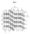
- FIG. 2shows a second embodiment of the memory cell array of the present invention.
- the arrangement of the word lines 2 , isolation gate lines 3 and bit lines 8 in FIG. 2is the same as that in FIG. 1 .
- the function of the isolation gate lines 3is the same as in FIG. 1 . Accordingly, a description thereof is omitted.
- the continuous active area linesare not formed as straight lines but as angled lines.
- each of the continuous active area lineswhich are generally formed in parallel to each other, comprises horizontal portions as well as slanted portions.
- the active area linescould as well comprise only slanted portions having, for example, two different angles with respect to the bit lines 8 .
- the portions of the active area lines lying in the portion between two neighboring bit lines 8are arranged horizontally whereas the portions of the active area lines, which are crossed by the bit lines 8 , intersect the bit lines in an angled manner.
- the portions of the active area lines lying in the spaces between adjacent bit linescould have a smaller angle with respect to the bit lines whereas the portions of the active area lines which are crossed by the bit lines, could have a larger angle with respect to the bit lines 8 .
- the contact area of the bit line contactswhich are formed at an intersection of the active area lines and the bit lines, can be made larger whereby the contact resistance is decreased.
- the node contacts 42are placed in the spaces between neighboring bit lines so that a contact to the second source/drain regions of the transistors can be easily achieved.
- FIG. 3shows an embodiment of the invention by means of a cross-section of the memory cell array of FIG. 1 between points III and III in FIG. 1 according to a first implementation of the memory cell, which is for example known from U.S. Pat. No. 6,545,904.
- the word linecan be formed of a polysilicon layer 22 , a layer 23 having a high conductivity such as a metallic layer, and an isolating layer 24 .
- the word line 2is electrically isolated from the adjacent bit line contact 41 and the adjacent node contact 42 by a spacer 411 made of an isolating material.
- the node contact 42is provided so as to accomplish an electrical contact between the second source/drain region 52 and a storage electrode of a storage capacitor (not shown).
- the bit line contact 41is associated with two neighboring transistors.
- the access transistor 61 or 62is addressed or activated, so that a current flows between the first and the second source/drain regions 51 , 52 .
- the electrical charge stored in the storage capacitor(not shown), which is electrically connected with the node contact 42 , can be read out and transferred to a bit line via the bit line contact 41 .
- FIG. 4shows a further embodiment of the present invention, in which the single memory cells are implemented in a different manner.
- the left part of FIG. 4shows a cross-section between I and I in FIG. 1
- the right part of FIG. 4shows a cross-section between II and II in FIG. 1 .
- the word lines 2 and the isolation gate lines 3are implemented as buried word lines and buried isolation gate lines, respectively.
- the top surface of the word lines 2 and the top surface of the isolation gate lines 3are disposed beneath the surface of the semiconductor substrate.
- the first access transistor 61comprises a first source/drain region 51 and a second source/drain region 52 , which are both implemented as n-doped portions.
- the channel 53 or channel regionis formed in the p-doped substrate portion between the first and the second source/drain regions 51 , 52 and the conductivity of the channel is controlled by applying an appropriate voltage to the word line 2 .
- the word line 2comprises a gate dielectric 21 for isolating the word line 2 from the channel 53 and additionally comprises a high conductivity layer 23 such as a metallic layer.
- An insulating layer 24is disposed above the high conductivity layer 23 so as to electrically isolate the word line from the first and second source/drain regions 51 , 52 .
- the access transistor 62comprises a first and a second source/drain regions 51 , 52 ′, as well as a channel 53 in the p-doped substrate portion between the first and the second source/drain regions.
- the conductivity of the channel 53is controlled by the word line 2 having an identical construction to the word line of the first access transistor.
- the isolation gate line 3comprises a gate dielectric 31 as well as a high conductivity layer 33 .
- An insulating layer 34is disposed above the high conductivity layer 33 so as to accomplish an electric isolation from the adjacent source/drain regions.
- An appropriate voltageis usually applied to the isolation gate line 3 so as to prevent an electrical current from flowing between the second source/drain region 52 ′, and the second source/drain region 52 of the access transistor disposed on the right hand side of the second access transistor 62 .
- a node contact 42connects the second source/drain regions 52 , 52 ′ with the storage electrode of a storage capacitor 63 .
- the storage capacitoris implemented as a stacked capacitor comprising a first storage electrode 631 , which is connected with the node contact 42 , a second storage electrode 632 , and a capacitor dielectric 633 which is disposed between the first and second storage electrodes 631 , 632 , and electrically isolates the two storage electrodes from each other.
- the two access transistors 61 , 62have a common bit line contact 41 .
- the bit line contact 41may be formed of doped polysilicon or another conducting material.
- the bit line 8which extends in a direction oblique to the plane of the drawing, is disposed above the bit line contact.
- the bit line 8can be made of an arbitrary conducting material.
- the bit line 8can be made of a layer stack which is similar or identical to a commonly used gate stack.
- the bit line 8 including the bit line contact 41can be made of a layer stack comprising a polysilicon layer, a highly conductive layer as well as an isolating layer so that it is formed in a similar manner as the word lines 2 which are shown in FIG. 3 .
- the gate electrodes of the transistors formed in a peripheral portion of the memory deviceare made of the same layer stack as the bit lines including the bit line contacts formed in the memory cell array.
- FIG. 4shows a cross-section of the memory cell array of FIG. 1 between II and II.
- the active area line 4is defined by two adjacent isolation trenches 5 which are filled with an isolating material such as SiO 2 .
- a word linecomprising a gate dielectric 21 , a high conductivity layer 23 as well as an insulating layer 24 is formed above the active area line and the adjacent isolation trenches 5 .
- a bit line 8is formed above the insulating layer 24 .
- the word lines 2 , the isolation gate lines 3 as well as the bit lines 8extend in directions which are oblique with respect to the plane of the drawing.
- the memory cell array of the present inventioncan be applied to a plurality of different implementations of the individual memory cells.
- FIG. 5is a simplified schematic diagram describing a pair of memory cell arrays 60 , 60 ′ in accordance with the present invention.
- the arraysare implemented in an open bit line configuration, each employing memory cells 6 formed from one transistor 61 and one capacitor 63 .
- the memory arrays 60 , 60 ′are each coupled to respective groups of bit lines 8 , 8 ′ and respective groups of word lines 2 , 2 ′.
- the two groups of bit lines 8 , 8 ′are coupled, one from each of the memory arrays 60 , 60 ′, to sense amplifiers 7 .
- the sense amplifiers 7comprise peripheral circuitry, i.e., circuitry employed in support of the memory arrays 60 , 60 ′ and generally are formed outside of peripheries of the memory arrays 60 , 60 ′.
- one memory cell 6is selected, for example, by activating one word line 2 .
- the word line 2is coupled to a respective gate electrode of a respective one of the transistors 61 .
- the bit line 8is coupled to the first source/drain region of one of these transistors 61 via the bit line contact 41 .
- the transistor 61is then turned on, coupling charge stored in the capacitor 63 to the associated bit line 8 .
- the sense amplifier 7then senses the charge coupled from the capacitor 63 to the bit line 8 .
- the sense amplifier 7compares that signal to a reference signal such as the reference charge Qref or a reference signal which is obtained by sensing a corresponding bit line 8 ′, without a voltage being applied to the corresponding word line 8 ′, amplifies the resulting signal and latches the amplified signal from appropriate duration.
- a reference signalsuch as the reference charge Qref or a reference signal which is obtained by sensing a corresponding bit line 8 ′, without a voltage being applied to the corresponding word line 8 ′
- Thisallows data represented by the charge stored in the capacitor 63 to be accessed external to the memory arrays 60 , 60 ′ and also allows the capacitor 63 to store charge representative of the data from the memory cell 6 back into the memory cell 6 .
- an alternative array architecturesuch as a vertically twisted bit line array architecture, which is generally known, can be used as well.
Landscapes
- Engineering & Computer Science (AREA)
- Microelectronics & Electronic Packaging (AREA)
- Computer Hardware Design (AREA)
- Semiconductor Memories (AREA)
Abstract
Description
- The invention relates to memory cell arrays comprising a plurality of memory cells such as, for example, DRAM (Dynamic Random Access) memory cells.
- Memory cells of a dynamic random access memory (DRAM) generally comprise a storage capacitor for storing an electrical charge which represents information to be stored, and an access transistor connected to the storage capacitor. The access transistor comprises first and a second source/drain regions, a channel connecting the first and second source/drain regions, and a gate electrode controlling an electrical current flowing between the first and second source/drain regions. The transistor usually is at least partially formed in a semiconductor substrate. The portion in which the transistor is formed generally is denoted as the active area. The gate electrode forms part of a word line, and the gate electrode is electrically isolated from the channel by a gate dielectric. By addressing the access transistor via the corresponding word line, the information stored in the storage capacitor is read out. In particular, the information is read out to a corresponding bit line via a bit line contact.
- In currently-used DRAM memory cells, the storage capacitor can be implemented as a trench capacitor in which the two capacitor electrodes are disposed in a trench which extends into the substrate in a direction perpendicular to the substrate surface. According to another implementation of a DRAM memory cell, the electrical charge is stored in a stacked capacitor, which is formed above the surface of the substrate.
- Generally, a DRAM memory cell array having a higher packaging density is desirable. For example U.S. Pat. No. 6,419,948, the disclosure of which is incorporated herein by reference in its entirety, discloses a memory cell array in which the active area is formed as a continuous line. The active area line and the bit line are formed as waving lines, so that one bit line and one corresponding active area line intersect at many points. According to this layout, the memory cells can have an area of about 6 F2, wherein F denotes the minimum pitch according to the technology used.
- In addition, U.S. Pat. No. 6,545,904, the disclosure of which is incorporated herein by reference in its entirety, discloses a memory cell including an access transistor and a storage capacitor which can be formed so as to implement a 6 F2(6 F*F) DRAM array. In particular, two neighboring access transistors are arranged, so that they have one common bit line contact. In addition, neighboring access transistors formed on a single active area line are electrically isolated from each other by an isolation gate line.
- DE 199 28 781 C1 discloses a 6 F2memory cell in which two adjacent memory cells share one common bit line contact. Two neighboring pairs of memory cells which are assigned to one active area line are separated and electrically isolated from each other by a groove which is filled with an isolating material.
- Furthermore, U.S. Pat. No. 5,502,320, the disclosure of which is incorporated herein by reference in its entirety, discloses a memory cell array in which transistors are formed in continuous active area lines. The active area lines are arranged in parallel with the bit lines. Two adjacent pairs of neighboring memory cells are separated and isolated from each other by applying an appropriate voltage to isolation gate lines which are arranged between the two adjacent pairs of memory cells. The word lines and the isolation gate lines are implemented as buried word lines and buried isolation gate lines, respectively.
- According to the present invention a memory cell array having a high packaging density and which can be easily fabricated comprises: memory cells each comprising a storage element and an access transistor, bit lines running along a first direction, word lines running along a second direction, the second direction being perpendicular to the first direction, a semiconductor substrate, continuous active area lines and isolation trenches being formed in said semiconductor substrate, said isolation trenches being adjacent to the active area lines, and the isolation trenches being adapted to electrically isolate neighboring active area lines from each other, the access transistors being at least partially formed in the active area lines and electrically coupling corresponding storage elements to corresponding bit lines via bit line contacts, the transistors being addressed by the word lines, the bit line contacts being formed in a region generally defined by an intersection of a bit line and a corresponding active area line, wherein neighboring bit line contacts, each connected with one active area line, are connected with neighboring bit lines.
- Accordingly, the present invention provides a memory cell array in which the transistors of the memory cells are formed in continuous active area lines. In other word, the active area lines are formed so that they extend continuously from one edge of the memory cell array to another edge of the memory cell array. Usually, neighboring active area lines are separated and electrically isolated from each other by isolation trenches while are filled with an isolating material such as silicon dioxide. Accordingly, a plurality of transistors is formed in one continuous active area line. This is in contrast to known memory cell arrays in which the active area line is divided into segments which are electrically isolated from each other by an isolating material and in which each of the segments comprises one or two transistors.
- The memory cell array of the present invention is advantageous with respect to known memory cell arrays since it is much easier to lithographically define active area lines instead of segments of active areas.
- According to the present invention, when being regarded in a three-dimensional cross-section, the bit lines are arranged in a plane which lies above the active areas. Nevertheless, when being regarded in a two-dimensional plan view, each of the active area lines is arranged in such a manner that it intersects a plurality of bit lines. A bit line contact is formed at an intersection of a bit line and a corresponding active area, and the active area line is arranged in such a manner that neighboring bit line contacts, which are associated to one active area line, are connected with neighboring bit lines. In particular, if the first bit line contact which is associated with a first active area line, is connected with the first bit line, then the second bit line contact of the first active area line is connected with the second bit line, the third bit line contact of the first active area line is connected with the third bit line, and so on.
- According to the present invention, the active area lines can be formed as straight lines. Nevertheless, it is also possible that the active area lines are formed as angled lines having different angles with respect to the bit lines, for example. To be more specific, the active area lines can be formed in parallel with the bit lines at predetermined portions of the active area lines and they can have a certain angle with respect to the bit lines at other portions of the active area lines. Alternatively, the active area lines can have a first angle with respect to the bit lines at first portions of the active area lines, and they can have a second angle with respect to the bit lines at second portions of the active area lines.
- Nevertheless, it is especially preferred to form the active area lines as straight lines. In this case, they can be lithographically defined more easily.
- On the other hand, if the active area lines are implemented as angled lines, a contact area of the bit line contacts can be enlarged whereby a contact resistance is reduced.
- According to the present invention, the memory cells can be implemented as DRAM memory cells comprising a storage capacitor and an access transistor. In particular, the storage capacitor can be a trench capacitor or a stacked capacitor which is disposed above the substrate surface.
- The present invention is highly advantageous for memory cells comprising a stacked capacitor since in this case the contact plugs for connecting the transistor with the corresponding storage capacitor can be defined very easily.
- Nevertheless, the present invention can be equally applied to different types of memory cells such as generally known in the art, such as MRAM (“magnetic random access memories”), FeRAM (“ferroelectric random access memories”), PCRAM (“phase changing random access memories”) in which the storage element is implemented in a different manner.
- According to a preferred embodiment to a present invention, an angle between the active area lines and the bit lines amounts to 10 to 60°. If the active area lines are not implemented as straight lines, this angle is measured between a straight line connecting the starting point and the end point of the active area lines and the bit lines. An angle from 10 to 25° is especially preferred.
- According to a further preferred embodiment of the present invention, one bit line contact is associated to two neighboring transistors of one active area line. In this case, the memory cell array can be implemented in a very dense manner. In this case, it is especially preferred, that the angle between the active area lines and the bit lines amounts to approximately 18°, in particular, 18.43°.
- According to a further preferred embodiment of the present invention, part of the word lines act as isolation gate lines which are adapted to isolate neighboring transistors from each other. In particular, it is especially preferred that every third word line acts as such an isolation gate line so that pairs of adjacent memory cells are isolated from each other.
- By applying an appropriate voltage to the isolation gate lines, a current is prevented from flowing across the active area line lying beneath the isolation gate line. As a consequence, memory cells adjacent to the isolation gate line are electrically isolated from each other.
- If pairs of memory cells are isolated from each other, it is especially preferred that the two memory cells belonging to one pair of memory cells share one common bit line contact. According to the present invention, a memory cell array is further provided, the memory cell array comprising memory cells, each of said memory cells comprising a storage element and an access transistor, the memory cell array further comprising bit lines running along a first direction, the bit lines being formed as straight bit lines, a semiconductor substrate, continuous active area lines and isolation trenches being formed in said semiconductor substrate, the isolation trenches being adjacent to the active area lines, and the isolation trenches being adapted to electrically isolate neighboring active area lines from each other, the access transistors being at least partially formed in the active area lines and electrically coupling corresponding storage elements to corresponding bit lines via bit line contacts, the transistors being addressed by the word lines, the bit line contacts being formed in a region generally defined by an intersection of a bit line and a corresponding active area line, wherein neighboring bit line contacts, each of which is connected with one active area line, are connected with neighboring bit lines.
- Accordingly, the present invention provides a memory cell in which the bit lines are formed as straight lines. In addition, the continuous active area lines are formed so as to intersect a plurality of bit lines forming a bit line contact at an intersection of a bit line and a corresponding active area line. According to the present invention, neighboring bit line contacts which are associated with one active area line are connected with neighboring bit lines. Differently stated, if the first bit line contact which is associated with a first active area line is connected with the first bit line, then the second bit line contact of the first active area line is connected with the second bit line, the third bit line contact of the first active area line is connected with the third bit line, and so on.
- The memory cell array of the present invention preferably further comprises a plurality of word lines wherein the transistors are addressed by these word lines.
- According to a preferred embodiment to a present invention, an angle between the active area lines and the bit lines amounts to 10 to 60°. If the active area lines are not implemented as straight lines, this angle is measured between a straight line connecting the starting point and the end point of the active area lines and the bit lines. An angle from 10 to 25° is especially preferred.
- According to a further preferred embodiment of the present invention, one bit line contact is associated to two neighboring transistors of one active area line. In this case, the memory cell array can be implemented in a very dense manner. In this case, it is especially preferred, that the angle between the active area lines and the bit lines amounts to approximately 18°, in particular, 18.43°.
- The features and advantages of the invention will become more readily apparent from a consideration of the following detailed description said forth with reference to the accompanying drawings which specify and show preferred embodiments of the invention, wherein like elements are designed by identical references throughout the drawings; and in which:
FIG. 1 shows a first preferred embodiment of the present invention;FIG. 2 shows a second preferred embodiment of the present invention;FIG. 3 shows a cross-section of a memory cell array according to a first preferred implementation of the individual memory cells;FIG. 4 shows a cross-section of a memory cell array according to a second preferred implementation of the individual memory cells; andFIG. 5 shows a schematic circuit representing a memory cell array of the present invention.FIG. 1 shows a first embodiment of the memory cell array of the present invention. InFIG. 1 , a plurality ofbit lines 8 are formed along a horizontal direction, whereas a plurality ofword lines 2 are arranged in a second direction which is preferably perpendicular to the first direction. In addition, continuousactive area lines 4 are disposed at a slanted angle with respect to the bit lines and the word lines, respectively. As is shown inFIG. 1 , thebit lines 8 as well as theword lines 2 are implemented as straight lines.- Usually, the active area lines are defined by forming
isolation trenches 5 which are filled with an isolating material, in a semiconductor substrate such as a silicon substrate. Accordingly, theactive area lines 4 are separated and electrically isolated from each other. At an intersection of anactive area line 4 and abit line 8, abit line contact 41 is formed. Moreover,node contacts 42 are formed at those portions of the active area lines which are not covered by abit line 8 nor by aword line 3. The node contact provides an electrical contact between an access transistor and a corresponding storage capacitor. Usually, the storage capacitor is formed on top of the shown semiconductor surface. - As is shown in
FIG. 1 , anisolation gate line 3 is disposed between pairs of neighboring word lines2. In a cross-section taken along I-I, theword lines 2 and theisolation gate lines 3 are disposed above the active area lines4. Transistors are formed in theactive area lines 4, wherein the transistors comprise a first source/drain region, a second source/drain region as well as a channel connecting first and second source/drain regions. The conductivity of the channel between the first and the second source/drain regions is controlled by theword lines 2 and theisolation gate line 3. In particular, an appropriate voltage is applied to theisolation gate line 3, so that no current flows beneath the isolation gate line. Accordingly, an electrical isolation between neighboring pairs of memory cells is achieved by the isolation gate line. The first and the second drain regions are arranged beneath thebit line contact 41 and thenode contact 42, respectively. - As is shown in
FIG. 1 , theword lines 2, theisolation gate lines 3 and thebit lines 8 are arranged in a regular manner so as to form a grid. - In the arrangement shown in
FIG. 1 , two adjacent transistors share a commonbit line contact 41, as will also be explained later. - The size of a single memory cell is typically described in terms of its minimal feature size (F). Usually, it is intended to implement the conductive lines so that they have a width equal to the minimal feature size and that they have a distance from each other which is equal to the minimal feature size. Accordingly, the sum of the isolation space between the conductive lines and the width of the conductive lines corresponds to the double of the feature size of the memory device. Currently, the feature size amounts to about 100 nm, a reduction of this feature size being aimed at. In particular, future memory devices will have feature sizes of 50 nm and below.
- In the memory cell array in
FIG. 1 , the width of each cell along the word line direction is 2 F, whereas the width along the bit line direction is 3 F. This results in a cell size of 6 F2(6 F*F). - As can be seen from
FIG. 1 , since twonode contacts 42 are followed by onebit line contact 41 and two neighboring bit line contacts of oneactive area line 4 are assigned to twodifferent bit lines 8, a horizontal distance of neighboring bit line contacts preferably amounts to 6 F, whereas a vertical distance of neighboring bit line contacts preferably amounts to 2 F. As a consequence, an angle between thebit line 8 and theactive area line 4 of about 18°, in particular 18,43°, is especially preferred, since 18.43° amounts to arctan(1/3). - The memory cell device of
FIG. 1 can be implemented very easily, since the active area is formed as a straight line. Accordingly, it can be lithographically defined in a simple manner, because only masks having a stripe pattern need to be used. To be more specific, in this case, the masks have a pattern of lines and spaces. In addition, since thebit line contact 41 is formed at an angled intersection between the active area line and the bit line, the contact area can be increased, whereby a contact resistance is decreased. FIG. 2 shows a second embodiment of the memory cell array of the present invention. The arrangement of theword lines 2,isolation gate lines 3 andbit lines 8 inFIG. 2 is the same as that inFIG. 1 . In addition, the function of theisolation gate lines 3 is the same as inFIG. 1 . Accordingly, a description thereof is omitted. As can be seen fromFIG. 2 , the continuous active area lines are not formed as straight lines but as angled lines. In particular, each of the continuous active area lines, which are generally formed in parallel to each other, comprises horizontal portions as well as slanted portions. As a modification, the active area lines could as well comprise only slanted portions having, for example, two different angles with respect to the bit lines8.- As is shown in
FIG. 2 , the portions of the active area lines lying in the portion between two neighboringbit lines 8 are arranged horizontally whereas the portions of the active area lines, which are crossed by thebit lines 8, intersect the bit lines in an angled manner. According to a modification, the portions of the active area lines lying in the spaces between adjacent bit lines could have a smaller angle with respect to the bit lines whereas the portions of the active area lines which are crossed by the bit lines, could have a larger angle with respect to the bit lines8. - In the memory all array of
FIG. 2 , the contact area of the bit line contacts, which are formed at an intersection of the active area lines and the bit lines, can be made larger whereby the contact resistance is decreased. In addition, thenode contacts 42 are placed in the spaces between neighboring bit lines so that a contact to the second source/drain regions of the transistors can be easily achieved. - As can be seen from
FIG. 2 , the memory cell size amounts to 6 F2as is also the case inFIG. 1 . FIG. 3 shows an embodiment of the invention by means of a cross-section of the memory cell array ofFIG. 1 between points III and III inFIG. 1 according to a first implementation of the memory cell, which is for example known from U.S. Pat. No. 6,545,904.- In a
semiconductor substrate 1, first andsecond access transistors first access transistor 61 comprises a first source/drain region 51 and a second source/drain region 52. The first and the second source/drain regions are implemented as n-doped portions. The channel or channel region is formed in the p-doped substrate portion between the first and the second source/drain regions word line 2. The word lines2 are isolated from the channel by agate dielectric 21. - As is shown in
FIG. 3 , the word line can be formed of apolysilicon layer 22, alayer 23 having a high conductivity such as a metallic layer, and an isolatinglayer 24. Theword line 2 is electrically isolated from the adjacentbit line contact 41 and theadjacent node contact 42 by aspacer 411 made of an isolating material. Thenode contact 42 is provided so as to accomplish an electrical contact between the second source/drain region 52 and a storage electrode of a storage capacitor (not shown). Thebit line contact 41 is associated with two neighboring transistors. Thesecond access transistor 62 likewise comprises first and second source/drain regions gate electrode 2 for controlling an electrical current flowing between the first and second source/drain regions, abit line contact 41 which also serves as a bit line contact of the access transistor disposed on the right side of the shownaccess transistor 62 as well as anode contact 42 for electrically connecting the second source/drain region 52′ with the storage electrode of a storage capacitor (not shown). Anisolation gate line 3 is disposed between the first and thesecond access transistors isolation gate line 3, so as to prevent an electrical current from flowing between the second source/drain regions polysilicon layer 22, a highlyconductive layer 23 and an isolatinglayer 24. Theisolation gate line 3 is isolated from the substrate by agate dielectric 31. - By applying an appropriate voltage to the
gate electrode 2 theaccess transistor drain regions node contact 42, can be read out and transferred to a bit line via thebit line contact 41. FIG. 4 shows a further embodiment of the present invention, in which the single memory cells are implemented in a different manner. The left part ofFIG. 4 shows a cross-section between I and I inFIG. 1 , whereas the right part ofFIG. 4 shows a cross-section between II and II inFIG. 1 . As is shown inFIG. 4 , theword lines 2 and theisolation gate lines 3 are implemented as buried word lines and buried isolation gate lines, respectively. In other words, the top surface of theword lines 2 and the top surface of theisolation gate lines 3 are disposed beneath the surface of the semiconductor substrate.- In
FIG. 4 , thefirst access transistor 61 comprises a first source/drain region 51 and a second source/drain region 52, which are both implemented as n-doped portions. Thechannel 53 or channel region is formed in the p-doped substrate portion between the first and the second source/drain regions word line 2. Theword line 2 comprises agate dielectric 21 for isolating theword line 2 from thechannel 53 and additionally comprises ahigh conductivity layer 23 such as a metallic layer. An insulatinglayer 24 is disposed above thehigh conductivity layer 23 so as to electrically isolate the word line from the first and second source/drain regions access transistor 62 comprises a first and a second source/drain regions channel 53 in the p-doped substrate portion between the first and the second source/drain regions. The conductivity of thechannel 53 is controlled by theword line 2 having an identical construction to the word line of the first access transistor. - Since the
word lines 2 are formed as buried word lines, thechannel 53 is formed in the shape of a “U”, whereby a channel length is increased. - On the right side of the second source/
drain region 52′ anisolation gate line 3 is disposed. Theisolation gate line 3 comprises agate dielectric 31 as well as ahigh conductivity layer 33. An insulatinglayer 34 is disposed above thehigh conductivity layer 33 so as to accomplish an electric isolation from the adjacent source/drain regions. An appropriate voltage is usually applied to theisolation gate line 3 so as to prevent an electrical current from flowing between the second source/drain region 52′, and the second source/drain region 52 of the access transistor disposed on the right hand side of thesecond access transistor 62. - In a similar manner as in
FIG. 3 a node contact 42 connects the second source/drain regions storage capacitor 63. As can be seen fromFIG. 4 , the storage capacitor is implemented as a stacked capacitor comprising afirst storage electrode 631, which is connected with thenode contact 42, asecond storage electrode 632, and acapacitor dielectric 633 which is disposed between the first andsecond storage electrodes - The two
access transistors bit line contact 41. Thebit line contact 41 may be formed of doped polysilicon or another conducting material. Thebit line 8 which extends in a direction oblique to the plane of the drawing, is disposed above the bit line contact. Thebit line 8 can be made of an arbitrary conducting material. In particular, thebit line 8 can be made of a layer stack which is similar or identical to a commonly used gate stack. For example, thebit line 8 including thebit line contact 41 can be made of a layer stack comprising a polysilicon layer, a highly conductive layer as well as an isolating layer so that it is formed in a similar manner as theword lines 2 which are shown inFIG. 3 . In this case, it is especially preferred that the gate electrodes of the transistors formed in a peripheral portion of the memory device are made of the same layer stack as the bit lines including the bit line contacts formed in the memory cell array. - The right hand part of
FIG. 4 shows a cross-section of the memory cell array ofFIG. 1 between II and II. As can be seen fromFIG. 4 , theactive area line 4 is defined by twoadjacent isolation trenches 5 which are filled with an isolating material such as SiO2. A word line comprising agate dielectric 21, ahigh conductivity layer 23 as well as an insulatinglayer 24 is formed above the active area line and theadjacent isolation trenches 5. Above the insulatinglayer 24, abit line 8 is formed. - On the left hand side of
FIG. 4 , an isolation groove44 is formed above theisolation gate line 3, so as to electrically isolate adjacent pairs of memory cells from each other. When theaccess transistor 61 is addressed by theword line 2, an electrical charge stored as an information in thestorage transistor 63 is read out via thenode contact 42 and transferred across theaccess transistor 61 from the second source/drain region 52 to the first source/drain region 51 and transferred to thebit line 8 via thebit line contact 41. - As is to noted from the left hand part of
FIGS. 3 and 4 in conjunction withFIG. 1 , theword lines 2, theisolation gate lines 3 as well as thebit lines 8 extend in directions which are oblique with respect to the plane of the drawing. - As will be apparent to the person skilled in the art, the memory cell array of the present invention can be applied to a plurality of different implementations of the individual memory cells.
FIG. 5 is a simplified schematic diagram describing a pair ofmemory cell arrays transistor 61 and onecapacitor 63.- The
memory arrays bit lines word lines bit lines memory arrays amplifiers 7. Thesense amplifiers 7 comprise peripheral circuitry, i.e., circuitry employed in support of thememory arrays memory arrays - In operation, one memory cell6 is selected, for example, by activating one
word line 2. Theword line 2 is coupled to a respective gate electrode of a respective one of thetransistors 61. Thebit line 8 is coupled to the first source/drain region of one of thesetransistors 61 via thebit line contact 41. Thetransistor 61 is then turned on, coupling charge stored in thecapacitor 63 to the associatedbit line 8. Thesense amplifier 7 then senses the charge coupled from thecapacitor 63 to thebit line 8. Thesense amplifier 7 compares that signal to a reference signal such as the reference charge Qref or a reference signal which is obtained by sensing acorresponding bit line 8′, without a voltage being applied to thecorresponding word line 8′, amplifies the resulting signal and latches the amplified signal from appropriate duration. This allows data represented by the charge stored in thecapacitor 63 to be accessed external to thememory arrays capacitor 63 to store charge representative of the data from the memory cell6 back into the memory cell6. As is obvious to the person skilled in the art, an alternative array architecture such as a vertically twisted bit line array architecture, which is generally known, can be used as well. - 1 semiconductor substrate
- 2,2′ word line
- 21 gate dielectric
- 22 poly-silicon
- 23 high conductivity layer
- 24 insulating
layer 8 - 3 isolation gate line
- 31 gate dielectric
- 4 active area line
- 41 bit line contact
- 411 spacer
- 42 node contact
- 43 poly-silicon
- 44 isolation groove
- 44 isolation trench
- 5 first source/drain region
- 52,52′ second source/drain region
- 6 memory cell
- 60,60′ memory cell array
- 61 first access transistor
- 62 second access transistor
- 63 storage capacitor
- 631 first capacitor electrode
- 632 second capacitor electrode
- 633 capacitor dielectric
- 7 sense amplifier
- 8,8′ bit line
Claims (21)
Priority Applications (7)
| Application Number | Priority Date | Filing Date | Title |
|---|---|---|---|
| US11/004,881US7139184B2 (en) | 2004-12-07 | 2004-12-07 | Memory cell array |
| TW094140852ATWI291700B (en) | 2004-12-07 | 2005-11-21 | Memory cell array |
| DE102005056427ADE102005056427A1 (en) | 2004-12-07 | 2005-11-28 | Memory cell array |
| KR1020050118170AKR100793932B1 (en) | 2004-12-07 | 2005-12-06 | Memory cell array |
| CN2005101310523ACN100407410C (en) | 2004-12-07 | 2005-12-07 | memory cell array |
| US11/562,315US7301799B2 (en) | 2004-12-07 | 2006-11-21 | Memory cell array |
| US11/945,437US7471547B2 (en) | 2004-12-07 | 2007-11-27 | Memory cell array |
Applications Claiming Priority (1)
| Application Number | Priority Date | Filing Date | Title |
|---|---|---|---|
| US11/004,881US7139184B2 (en) | 2004-12-07 | 2004-12-07 | Memory cell array |
Related Child Applications (1)
| Application Number | Title | Priority Date | Filing Date |
|---|---|---|---|
| US11/562,315ContinuationUS7301799B2 (en) | 2004-12-07 | 2006-11-21 | Memory cell array |
Publications (2)
| Publication Number | Publication Date |
|---|---|
| US20060120129A1true US20060120129A1 (en) | 2006-06-08 |
| US7139184B2 US7139184B2 (en) | 2006-11-21 |
Family
ID=36441896
Family Applications (3)
| Application Number | Title | Priority Date | Filing Date |
|---|---|---|---|
| US11/004,881Expired - LifetimeUS7139184B2 (en) | 2004-12-07 | 2004-12-07 | Memory cell array |
| US11/562,315Expired - Fee RelatedUS7301799B2 (en) | 2004-12-07 | 2006-11-21 | Memory cell array |
| US11/945,437Expired - LifetimeUS7471547B2 (en) | 2004-12-07 | 2007-11-27 | Memory cell array |
Family Applications After (2)
| Application Number | Title | Priority Date | Filing Date |
|---|---|---|---|
| US11/562,315Expired - Fee RelatedUS7301799B2 (en) | 2004-12-07 | 2006-11-21 | Memory cell array |
| US11/945,437Expired - LifetimeUS7471547B2 (en) | 2004-12-07 | 2007-11-27 | Memory cell array |
Country Status (5)
| Country | Link |
|---|---|
| US (3) | US7139184B2 (en) |
| KR (1) | KR100793932B1 (en) |
| CN (1) | CN100407410C (en) |
| DE (1) | DE102005056427A1 (en) |
| TW (1) | TWI291700B (en) |
Cited By (10)
| Publication number | Priority date | Publication date | Assignee | Title |
|---|---|---|---|---|
| US20080061322A1 (en)* | 2006-09-08 | 2008-03-13 | Von Kluge Johannes | Transistor, memory cell array and method of manufacturing a transistor |
| US20080111174A1 (en)* | 2006-11-14 | 2008-05-15 | Qimonda Ag | Memory device and a method of manufacturing the same |
| US20080121961A1 (en)* | 2006-09-08 | 2008-05-29 | Till Schloesser | Transistor and memory cell array |
| US20080258206A1 (en)* | 2007-04-17 | 2008-10-23 | Qimonda Ag | Self-Aligned Gate Structure, Memory Cell Array, and Methods of Making the Same |
| US20090073736A1 (en)* | 2007-09-18 | 2009-03-19 | Samsung Electronics Co., Ltd. | Semiconductor device having storage nodes on active regions and method of fabricating the same |
| WO2019005135A1 (en)* | 2017-06-30 | 2019-01-03 | Intel Corporation | Usage of trench contact in read only memory programming |
| US10872858B2 (en) | 2017-08-30 | 2020-12-22 | United Microelectronics Corp. | Semiconductor memory device |
| US11062771B2 (en)* | 2007-04-03 | 2021-07-13 | Ovonyx Memory Technology, Llc | Variable resistance memory with lattice array using enclosing transistors |
| US20230397408A1 (en)* | 2022-06-02 | 2023-12-07 | Micron Technology, Inc. | Apparatuses including semiconductive pillar structures, and related methods, memory devices, and electronic systems |
| US12279433B2 (en) | 2021-08-09 | 2025-04-15 | Samsung Electronics Co., Ltd. | Semiconductor device |
Families Citing this family (36)
| Publication number | Priority date | Publication date | Assignee | Title |
|---|---|---|---|---|
| US5673218A (en) | 1996-03-05 | 1997-09-30 | Shepard; Daniel R. | Dual-addressed rectifier storage device |
| US6956757B2 (en) | 2000-06-22 | 2005-10-18 | Contour Semiconductor, Inc. | Low cost high density rectifier matrix memory |
| US7476920B2 (en)* | 2004-12-15 | 2009-01-13 | Infineon Technologies Ag | 6F2 access transistor arrangement and semiconductor memory device |
| US7593256B2 (en)* | 2006-03-28 | 2009-09-22 | Contour Semiconductor, Inc. | Memory array with readout isolation |
| KR100763336B1 (en)* | 2006-09-27 | 2007-10-04 | 삼성전자주식회사 | Method of disposing a semiconductor memory device and a memory cell array thereof |
| US7605037B2 (en)* | 2007-02-09 | 2009-10-20 | Qimonda Ag | Manufacturing method for an integrated semiconductor memory device and corresponding semiconductor memory device |
| US7642572B2 (en)* | 2007-04-13 | 2010-01-05 | Qimonda Ag | Integrated circuit having a memory cell array and method of forming an integrated circuit |
| US7813157B2 (en) | 2007-10-29 | 2010-10-12 | Contour Semiconductor, Inc. | Non-linear conductor memory |
| KR20090090597A (en)* | 2008-02-21 | 2009-08-26 | 삼성전자주식회사 | Ferroelectric memory device and manufacturing method thereof |
| US20090321805A1 (en)* | 2008-06-30 | 2009-12-31 | Qimonda Ag | Insulator material over buried conductive line |
| US8325556B2 (en) | 2008-10-07 | 2012-12-04 | Contour Semiconductor, Inc. | Sequencing decoder circuit |
| US8294188B2 (en)* | 2008-10-16 | 2012-10-23 | Qimonda Ag | 4 F2 memory cell array |
| KR101487966B1 (en)* | 2008-11-25 | 2015-02-03 | 삼성전자주식회사 | Three dimensional semiconductor memory device |
| KR101625924B1 (en)* | 2010-07-05 | 2016-05-31 | 에스케이하이닉스 주식회사 | Semiconductor device and method of manufacturing the same |
| US8519462B2 (en)* | 2011-06-27 | 2013-08-27 | Intel Corporation | 6F2 DRAM cell |
| US9401363B2 (en)* | 2011-08-23 | 2016-07-26 | Micron Technology, Inc. | Vertical transistor devices, memory arrays, and methods of forming vertical transistor devices |
| KR101887144B1 (en)* | 2012-03-15 | 2018-08-09 | 삼성전자주식회사 | Semiconductor device and Method of manufacturing the same |
| KR101325188B1 (en)* | 2012-04-09 | 2013-11-20 | 이화여자대학교 산학협력단 | Magnetic ramdom access memory |
| JP2014225566A (en)* | 2013-05-16 | 2014-12-04 | ピーエスフォー ルクスコ エスエイアールエルPS4 Luxco S.a.r.l. | Semiconductor device |
| CN104637945B (en)* | 2013-11-08 | 2018-08-03 | 苏州东微半导体有限公司 | Half floating-gate memory and its manufacturing method and half floating gate memory array |
| CN107785370A (en)* | 2016-08-30 | 2018-03-09 | 联华电子股份有限公司 | high density semiconductor structure |
| US10062745B2 (en)* | 2017-01-09 | 2018-08-28 | Micron Technology, Inc. | Methods of forming an array of capacitors, methods of forming an array of memory cells individually comprising a capacitor and a transistor, arrays of capacitors, and arrays of memory cells individually comprising a capacitor and a transistor |
| CN107093604A (en)* | 2017-04-27 | 2017-08-25 | 睿力集成电路有限公司 | Dynamic random access memory and its manufacture method |
| KR102358481B1 (en) | 2017-06-08 | 2022-02-04 | 삼성전자주식회사 | Semiconductor device and method for manufacturing the same |
| CN107240586B (en)* | 2017-07-26 | 2018-03-06 | 睿力集成电路有限公司 | Memory and forming method thereof, semiconductor devices |
| CN107611133B (en)* | 2017-10-16 | 2018-08-14 | 睿力集成电路有限公司 | Memory and forming method thereof, semiconductor devices |
| CN109698193B (en)* | 2017-10-24 | 2024-02-09 | 长鑫存储技术有限公司 | Array structure of semiconductor memory |
| CN107634057B (en)* | 2017-10-30 | 2018-10-16 | 睿力集成电路有限公司 | Dynamic random access memory array and its domain structure, production method |
| CN109979939B (en)* | 2017-12-27 | 2021-09-28 | 长鑫存储技术有限公司 | Semiconductor memory device structure and manufacturing method thereof |
| CN113451269B (en)* | 2020-03-25 | 2022-07-22 | 长鑫存储技术有限公司 | Word line structure and semiconductor memory |
| WO2021253716A1 (en) | 2020-06-19 | 2021-12-23 | 长鑫存储技术有限公司 | Storage unit and data reading and writing method therefor, and storage array |
| KR102831626B1 (en) | 2020-06-22 | 2025-07-07 | 창신 메모리 테크놀로지즈 아이엔씨 | How memory is formed and memory |
| CN113903709B (en) | 2020-06-22 | 2024-08-02 | 长鑫存储技术有限公司 | Memory forming method and memory |
| CN114388503B (en)* | 2020-10-16 | 2024-10-15 | 长鑫存储技术有限公司 | Semiconductor device and method for manufacturing the same |
| CN114639772A (en) | 2020-12-15 | 2022-06-17 | 长鑫存储技术有限公司 | A semiconductor structure and memory circuit |
| CN114121959B (en)* | 2021-11-19 | 2024-11-26 | 北京超弦存储器研究院 | Storage device and manufacturing method thereof, and electronic device including the storage device |
Citations (5)
| Publication number | Priority date | Publication date | Assignee | Title |
|---|---|---|---|---|
| US5502320A (en)* | 1993-03-15 | 1996-03-26 | Kabushiki Kaisha Toshiba | Dynamic random access memory (DRAM) semiconductor device |
| US6419948B2 (en)* | 1995-01-13 | 2002-07-16 | Somerset Pharmaceuticals, Inc. | R(-)desmethylselegiline and its use in transdermal delivery compositions |
| US6545904B2 (en)* | 2001-03-16 | 2003-04-08 | Micron Technology, Inc. | 6f2 dram array, a dram array formed on a semiconductive substrate, a method of forming memory cells in a 6f2 dram array and a method of isolating a single row of memory cells in a 6f2 dram array |
| US6894915B2 (en)* | 2002-11-15 | 2005-05-17 | Micron Technology, Inc. | Method to prevent bit line capacitive coupling |
| US7020039B2 (en)* | 2002-08-29 | 2006-03-28 | Micron Technology, Inc. | Isolation device over field in a memory device |
Family Cites Families (15)
| Publication number | Priority date | Publication date | Assignee | Title |
|---|---|---|---|---|
| KR950003402B1 (en) | 1992-09-08 | 1995-04-12 | 삼성전자 주식회사 | Folded bit-line DRAM array |
| US6025221A (en)* | 1997-08-22 | 2000-02-15 | Micron Technology, Inc. | Processing methods of forming integrated circuitry memory devices, methods of forming DRAM arrays, and related semiconductor masks |
| US6035355A (en) | 1998-04-27 | 2000-03-07 | International Business Machines Corporation | PCI system and adapter requirements following reset |
| DE19843979C1 (en) | 1998-09-24 | 2000-03-02 | Siemens Ag | Memory cell array, for a FeRAM or DRAM, has trench bottom and ridge crest planar transistors with source regions connected by bit lines angled to word lines |
| DE19928781C1 (en) | 1999-06-23 | 2000-07-06 | Siemens Ag | DRAM cell array has deep word line trenches for increasing transistor channel length and has no fixed potential word lines separating adjacent memory cells |
| US6339241B1 (en)* | 2000-06-23 | 2002-01-15 | International Business Machines Corporation | Structure and process for 6F2 trench capacitor DRAM cell with vertical MOSFET and 3F bitline pitch |
| JP2002151665A (en)* | 2000-11-14 | 2002-05-24 | Hitachi Ltd | Semiconductor integrated circuit device and method of manufacturing the same |
| JP2003092364A (en) | 2001-05-21 | 2003-03-28 | Mitsubishi Electric Corp | Semiconductor storage device |
| US6590817B2 (en) | 2001-07-23 | 2003-07-08 | Micron Technology, Inc. | 6F2 DRAM array with apparatus for stress testing an isolation gate and method |
| KR100891249B1 (en)* | 2002-05-31 | 2009-04-01 | 주식회사 하이닉스반도체 | A semiconductor memory device having a 6F2 DRAM cell |
| JP2004193483A (en) | 2002-12-13 | 2004-07-08 | Renesas Technology Corp | Semiconductor storage device |
| JP2004213722A (en)* | 2002-12-27 | 2004-07-29 | Matsushita Electric Ind Co Ltd | Semiconductor storage device and semiconductor integrated circuit device |
| JP2004281736A (en) | 2003-03-17 | 2004-10-07 | Nec Electronics Corp | Semiconductor storage device |
| KR100555564B1 (en)* | 2004-03-31 | 2006-03-03 | 삼성전자주식회사 | Semiconductor element employing square storage electrode and its manufacturing method |
| KR100800137B1 (en)* | 2004-11-26 | 2008-02-01 | 주식회사 하이닉스반도체 | Memory elements |
- 2004
- 2004-12-07USUS11/004,881patent/US7139184B2/ennot_activeExpired - Lifetime
- 2005
- 2005-11-21TWTW094140852Apatent/TWI291700B/ennot_activeIP Right Cessation
- 2005-11-28DEDE102005056427Apatent/DE102005056427A1/ennot_activeWithdrawn
- 2005-12-06KRKR1020050118170Apatent/KR100793932B1/ennot_activeExpired - Fee Related
- 2005-12-07CNCN2005101310523Apatent/CN100407410C/ennot_activeExpired - Fee Related
- 2006
- 2006-11-21USUS11/562,315patent/US7301799B2/ennot_activeExpired - Fee Related
- 2007
- 2007-11-27USUS11/945,437patent/US7471547B2/ennot_activeExpired - Lifetime
Patent Citations (5)
| Publication number | Priority date | Publication date | Assignee | Title |
|---|---|---|---|---|
| US5502320A (en)* | 1993-03-15 | 1996-03-26 | Kabushiki Kaisha Toshiba | Dynamic random access memory (DRAM) semiconductor device |
| US6419948B2 (en)* | 1995-01-13 | 2002-07-16 | Somerset Pharmaceuticals, Inc. | R(-)desmethylselegiline and its use in transdermal delivery compositions |
| US6545904B2 (en)* | 2001-03-16 | 2003-04-08 | Micron Technology, Inc. | 6f2 dram array, a dram array formed on a semiconductive substrate, a method of forming memory cells in a 6f2 dram array and a method of isolating a single row of memory cells in a 6f2 dram array |
| US7020039B2 (en)* | 2002-08-29 | 2006-03-28 | Micron Technology, Inc. | Isolation device over field in a memory device |
| US6894915B2 (en)* | 2002-11-15 | 2005-05-17 | Micron Technology, Inc. | Method to prevent bit line capacitive coupling |
Cited By (16)
| Publication number | Priority date | Publication date | Assignee | Title |
|---|---|---|---|---|
| US7763514B2 (en) | 2006-09-08 | 2010-07-27 | Qimonda Ag | Method of manufacturing a transistor and memory cell array |
| US20080061320A1 (en)* | 2006-09-08 | 2008-03-13 | Qimonda Ag | Transistor, Memory Cell Array and Method of Manufacturing a Transistor |
| US20080121961A1 (en)* | 2006-09-08 | 2008-05-29 | Till Schloesser | Transistor and memory cell array |
| US20080061322A1 (en)* | 2006-09-08 | 2008-03-13 | Von Kluge Johannes | Transistor, memory cell array and method of manufacturing a transistor |
| US7956387B2 (en) | 2006-09-08 | 2011-06-07 | Qimonda Ag | Transistor and memory cell array |
| US7612406B2 (en) | 2006-09-08 | 2009-11-03 | Infineon Technologies Ag | Transistor, memory cell array and method of manufacturing a transistor |
| US20080111174A1 (en)* | 2006-11-14 | 2008-05-15 | Qimonda Ag | Memory device and a method of manufacturing the same |
| US11062771B2 (en)* | 2007-04-03 | 2021-07-13 | Ovonyx Memory Technology, Llc | Variable resistance memory with lattice array using enclosing transistors |
| US11763885B2 (en) | 2007-04-03 | 2023-09-19 | Ovonyx Memory Technology, Llc | Variable resistance memory with lattice array using enclosing transistors |
| US20080258206A1 (en)* | 2007-04-17 | 2008-10-23 | Qimonda Ag | Self-Aligned Gate Structure, Memory Cell Array, and Methods of Making the Same |
| US20090073736A1 (en)* | 2007-09-18 | 2009-03-19 | Samsung Electronics Co., Ltd. | Semiconductor device having storage nodes on active regions and method of fabricating the same |
| KR101353343B1 (en)* | 2007-09-18 | 2014-01-17 | 삼성전자주식회사 | Semiconductor Devices Having Storage Nodes Respectively Spaced away To Different Distances From One Side Of Bit Line Pattern On Active and Methods Of Forming The Same |
| WO2019005135A1 (en)* | 2017-06-30 | 2019-01-03 | Intel Corporation | Usage of trench contact in read only memory programming |
| US10872858B2 (en) | 2017-08-30 | 2020-12-22 | United Microelectronics Corp. | Semiconductor memory device |
| US12279433B2 (en) | 2021-08-09 | 2025-04-15 | Samsung Electronics Co., Ltd. | Semiconductor device |
| US20230397408A1 (en)* | 2022-06-02 | 2023-12-07 | Micron Technology, Inc. | Apparatuses including semiconductive pillar structures, and related methods, memory devices, and electronic systems |
Also Published As
| Publication number | Publication date |
|---|---|
| DE102005056427A1 (en) | 2006-06-08 |
| CN100407410C (en) | 2008-07-30 |
| US7471547B2 (en) | 2008-12-30 |
| US20080089114A1 (en) | 2008-04-17 |
| US20070155077A1 (en) | 2007-07-05 |
| US7301799B2 (en) | 2007-11-27 |
| TWI291700B (en) | 2007-12-21 |
| TW200625331A (en) | 2006-07-16 |
| KR100793932B1 (en) | 2008-01-16 |
| US7139184B2 (en) | 2006-11-21 |
| CN1815718A (en) | 2006-08-09 |
| KR20060063747A (en) | 2006-06-12 |
Similar Documents
| Publication | Publication Date | Title |
|---|---|---|
| US7139184B2 (en) | Memory cell array | |
| US12150312B2 (en) | Array of capacitors, array of memory cells, methods of forming an array of capacitors, and methods of forming an array of memory cells | |
| US7956387B2 (en) | Transistor and memory cell array | |
| US11922984B2 (en) | Memory device having volatile and non-volatile memory cells | |
| US7759704B2 (en) | Memory cell array comprising wiggled bit lines | |
| US8294188B2 (en) | 4 F2 memory cell array | |
| US20070290249A1 (en) | Integrated Circuit Including a Memory Cell Array | |
| US10998027B2 (en) | Memory circuitry | |
| US7863684B2 (en) | High integrated semiconductor memory device | |
| KR20210016641A (en) | Integrated circuit configuration | |
| US8508982B2 (en) | Semiconductor device | |
| US20070037345A1 (en) | Memory cell array and memory cell | |
| US7321514B2 (en) | DRAM memory cell arrangement | |
| US11437089B2 (en) | Integrated circuit devices | |
| US8072077B2 (en) | Semiconductor memory device | |
| KR100676200B1 (en) | Memory cell array, memory device, and plate voltage supply method having plate voltage insensitive to noise | |
| KR100900136B1 (en) | 1-transistor DRAM | |
| KR100486633B1 (en) | Semiconductor memory device having planar mos cell and folded bitline structure | |
| US20050270864A1 (en) | Memory cell arrangement having dual memory cells |
Legal Events
| Date | Code | Title | Description |
|---|---|---|---|
| AS | Assignment | Owner name:INFINEON TECHNOLOGIES AG, GERMANY Free format text:ASSIGNMENT OF ASSIGNORS INTEREST;ASSIGNOR:SCHLOESSER, TILL;REEL/FRAME:015577/0295 Effective date:20041221 | |
| STCF | Information on status: patent grant | Free format text:PATENTED CASE | |
| CC | Certificate of correction | ||
| AS | Assignment | Owner name:QIMONDA AG, GERMANY Free format text:ASSIGNMENT OF ASSIGNORS INTEREST;ASSIGNOR:INFINEON TECHNOLOGIES AG;REEL/FRAME:023806/0001 Effective date:20060425 Owner name:QIMONDA AG,GERMANY Free format text:ASSIGNMENT OF ASSIGNORS INTEREST;ASSIGNOR:INFINEON TECHNOLOGIES AG;REEL/FRAME:023806/0001 Effective date:20060425 | |
| FPAY | Fee payment | Year of fee payment:4 | |
| FPAY | Fee payment | Year of fee payment:8 | |
| AS | Assignment | Owner name:INFINEON TECHNOLOGIES AG, GERMANY Free format text:ASSIGNMENT OF ASSIGNORS INTEREST;ASSIGNOR:QIMONDA AG;REEL/FRAME:035623/0001 Effective date:20141009 | |
| AS | Assignment | Owner name:POLARIS INNOVATIONS LIMITED, IRELAND Free format text:ASSIGNMENT OF ASSIGNORS INTEREST;ASSIGNOR:INFINEON TECHNOLOGIES AG;REEL/FRAME:036908/0923 Effective date:20150708 | |
| MAFP | Maintenance fee payment | Free format text:PAYMENT OF MAINTENANCE FEE, 12TH YEAR, LARGE ENTITY (ORIGINAL EVENT CODE: M1553) Year of fee payment:12 |