US20060118779A1 - Organic Electronic Component Comprising A Patterned, Semi-Conducting Functional Layer And A Method For Producing Said Component - Google Patents
Organic Electronic Component Comprising A Patterned, Semi-Conducting Functional Layer And A Method For Producing Said ComponentDownload PDFInfo
- Publication number
- US20060118779A1 US20060118779A1US10/535,448US53544805AUS2006118779A1US 20060118779 A1US20060118779 A1US 20060118779A1US 53544805 AUS53544805 AUS 53544805AUS 2006118779 A1US2006118779 A1US 2006118779A1
- Authority
- US
- United States
- Prior art keywords
- functional layer
- patterned
- component
- organic electronic
- electronic component
- Prior art date
- Legal status (The legal status is an assumption and is not a legal conclusion. Google has not performed a legal analysis and makes no representation as to the accuracy of the status listed.)
- Granted
Links
- 239000002346layers by functionSubstances0.000titleclaimsabstractdescription43
- 238000004519manufacturing processMethods0.000titleclaimsabstractdescription7
- 239000010410layerSubstances0.000claimsabstractdescription13
- 238000000034methodMethods0.000claimsabstractdescription10
- 238000011282treatmentMethods0.000claimsabstractdescription8
- 239000000463materialSubstances0.000claimsdescription6
- 238000000059patterningMethods0.000claimsdescription3
- 238000009736wettingMethods0.000abstractdescription8
- 230000005669field effectEffects0.000abstractdescription4
- 238000000576coating methodMethods0.000description5
- 239000000758substrateSubstances0.000description4
- 239000011248coating agentSubstances0.000description3
- 239000004065semiconductorSubstances0.000description3
- 238000005507sprayingMethods0.000description3
- 239000000126substanceSubstances0.000description3
- 239000011368organic materialSubstances0.000description2
- OKTJSMMVPCPJKN-UHFFFAOYSA-NCarbonChemical compound[C]OKTJSMMVPCPJKN-UHFFFAOYSA-N0.000description1
- 239000002253acidSubstances0.000description1
- 230000004075alterationEffects0.000description1
- 229910052799carbonInorganic materials0.000description1
- 239000004020conductorSubstances0.000description1
- 238000010276constructionMethods0.000description1
- 230000000694effectsEffects0.000description1
- 229920001002functional polymerPolymers0.000description1
- 229910052732germaniumInorganic materials0.000description1
- GNPVGFCGXDBREM-UHFFFAOYSA-Ngermanium atomChemical compound[Ge]GNPVGFCGXDBREM-UHFFFAOYSA-N0.000description1
- 238000013532laser treatmentMethods0.000description1
- 239000002184metalSubstances0.000description1
- 125000002524organometallic groupChemical group0.000description1
- 230000000704physical effectEffects0.000description1
- 239000004033plasticSubstances0.000description1
- 229920003023plasticPolymers0.000description1
- 229920001296polysiloxanePolymers0.000description1
- 229910052710siliconInorganic materials0.000description1
- 239000010703siliconSubstances0.000description1
- 150000003384small moleculesChemical class0.000description1
- 238000004528spin coatingMethods0.000description1
- 238000007669thermal treatmentMethods0.000description1
Images

Classifications
- H—ELECTRICITY
- H10—SEMICONDUCTOR DEVICES; ELECTRIC SOLID-STATE DEVICES NOT OTHERWISE PROVIDED FOR
- H10K—ORGANIC ELECTRIC SOLID-STATE DEVICES
- H10K19/00—Integrated devices, or assemblies of multiple devices, comprising at least one organic element specially adapted for rectifying, amplifying, oscillating or switching, covered by group H10K10/00
- H10K19/10—Integrated devices, or assemblies of multiple devices, comprising at least one organic element specially adapted for rectifying, amplifying, oscillating or switching, covered by group H10K10/00 comprising field-effect transistors
- H—ELECTRICITY
- H10—SEMICONDUCTOR DEVICES; ELECTRIC SOLID-STATE DEVICES NOT OTHERWISE PROVIDED FOR
- H10K—ORGANIC ELECTRIC SOLID-STATE DEVICES
- H10K10/00—Organic devices specially adapted for rectifying, amplifying, oscillating or switching; Organic capacitors or resistors having potential barriers
- H10K10/40—Organic transistors
- H10K10/46—Field-effect transistors, e.g. organic thin-film transistors [OTFT]
- H10K10/462—Insulated gate field-effect transistors [IGFETs]
- H10K10/468—Insulated gate field-effect transistors [IGFETs] characterised by the gate dielectrics
- H—ELECTRICITY
- H10—SEMICONDUCTOR DEVICES; ELECTRIC SOLID-STATE DEVICES NOT OTHERWISE PROVIDED FOR
- H10K—ORGANIC ELECTRIC SOLID-STATE DEVICES
- H10K71/00—Manufacture or treatment specially adapted for the organic devices covered by this subclass
- H10K71/10—Deposition of organic active material
- H10K71/12—Deposition of organic active material using liquid deposition, e.g. spin coating
- H10K71/13—Deposition of organic active material using liquid deposition, e.g. spin coating using printing techniques, e.g. ink-jet printing or screen printing
- H—ELECTRICITY
- H10—SEMICONDUCTOR DEVICES; ELECTRIC SOLID-STATE DEVICES NOT OTHERWISE PROVIDED FOR
- H10K—ORGANIC ELECTRIC SOLID-STATE DEVICES
- H10K10/00—Organic devices specially adapted for rectifying, amplifying, oscillating or switching; Organic capacitors or resistors having potential barriers
- H10K10/40—Organic transistors
- H10K10/46—Field-effect transistors, e.g. organic thin-film transistors [OTFT]
- H10K10/462—Insulated gate field-effect transistors [IGFETs]
- H10K10/464—Lateral top-gate IGFETs comprising only a single gate
Definitions
- the inventionrelates to an organic electronic component such as an organic field effect transistor and a method for producing said component, the semiconducting layer of the component being patterned.
- the organic semiconducting functional layersare usually applied in large-area fashion by spin-coating, spraying on, squeegeeing or the like as homogeneous large-area but very thin functional layers.
- the semiconducting functional layercannot be applied in patterned fashion by conventional printing method because this layer must be very thin (typically less than 100 nm) in order for it to function.
- the layer thicknesses required for the semiconducting functional layercan conventionally be achieved only by means of a coating process such as coating, spraying on, etc.
- The, inventionrelates to an organic electronic component comprising a patterned semiconducting functional layer having a thickness of less than 100 nm, the patterning arising by virtue of a lower functional layer being only partially wetted with the organic functional material of the next functional layer.
- the inventionadditionally relates to a method for producing an organic electronic component, in which, through targeted treatment of a lower functional layer, an upper functional layer is produced in patterned fashion despite large-area application.
- a semiconducting layeris produced in patterned fashion.
- the lower functional layeris partially covered by a resist that can be applied with a very small layer thickness by printing.
- Semiconducting, insulating, and/or conductive organic functional layerscan be produced in patterned fashion by the method as upper, patterned functional layers.
- inorganic functional layerssuch as e.g. thin metal layers
- the lower functional layeris the substrate, a conductive functional layer, etc.
- targeted treatmentdenotes the partial coverage and/or the local alteration of the lower functional layer, which has the effect that, in selected regions of the lower functional layer, in the course, of coating with the material, wetting takes place or is avoided (that is to say “partial wetting” takes place), and can be effected by means of a printing method, by laser treatment, thermal treatment, other physical, electrical or chemical treatment, but always partially and with a resolution in the ⁇ m range.
- partial contact-making with acid/base or ocher reactive chemical substancesphysical effects such as light, heat, cold, and finally mechanical treatment such as rubbing.
- the treatmenthas the consequence in any event that tie next functional layer does not undergo wetting on the treated locations or undergoes wetting only there.
- organic materialand/or “functional polymer” here encompasses all types of organic, organometallic and/o inorganic plastics. It concerns all types of substances with the exception of the semiconductors that form the traditional diodes (germanium, silicon) and the typical metallic conductors. Accordingly, a restriction in the dogmatic sense to organic material as material containing carbon is not envisaged, rather the broad use of e.g. silicones is also conceived of. Furthermore, the term is not intended to be subject to any restriction with regard to the molecular size, in particular to polymeric and/or oligomeric materials, rather the use of “small molecules” is also entirely possible.
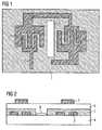
- FIG. 1shows a plan view of a circuit having a patterned semiconducting functional layer.
- An organic circuit constructed on a substrate (concealed)can be seen.
- a plurality of active elementssuch as organic field effect transistors are arranged one beside the other; the source/drain electrodes 2 can be discerned in each case.
- the hatched regionshows the organic semiconductor layer 1 , which is patterned and has partial regions 3 which are free of semiconducting functional material.
- the free region 3(“free” in this case means covered neither with conductive nor with semiconducting material) suppresses a leakage current from the left-hand region into the right-hand region of the circuit.
- FIG. 2shows an OFET having the substrate 4 and the source/drain electrodes 2 .
- the source/drain electrodes 2Situated on the conductive functional layer, the source/drain electrodes 2 , is the patterned semiconducting functional layer 1 , which does not extend over the conductive functional layer 2 in whole-area fashion, but rather is interrupted by the resist 6 , which partially covers the substrate 4 against wetting with semiconducting functional layer 1 , in other words said semiconducting functional layer covers in patterned fashion only the active areas, that is to say the areas above the source/drain electrodes.
- the semiconducting functional layer for its partis covered by the insulating functional layer 5 , on which the gate electrodes 7 are situated.
- the inventionrelates to an organic electronic component such as an organic field effect transistor and a method for producing said component, a thin layer, such as the semiconducting layer of the component being patterned, although the component can be produced-by an inexpensive printing method.
- the lower functional layeris prepared by a treatment such that it has partial regions on which betting takes place in the subsequent process step, and partial regions on which wetting is not effected.
Landscapes
- Engineering & Computer Science (AREA)
- Manufacturing & Machinery (AREA)
- Thin Film Transistor (AREA)
- Liquid Deposition Of Substances Of Which Semiconductor Devices Are Composed (AREA)
- Bipolar Transistors (AREA)
Abstract
Description
- The invention relates to an organic electronic component such as an organic field effect transistor and a method for producing said component, the semiconducting layer of the component being patterned.
- In the case of organic electronic components, the organic semiconducting functional layers are usually applied in large-area fashion by spin-coating, spraying on, squeegeeing or the like as homogeneous large-area but very thin functional layers.
- In an integrated circuit, that may lead to problems since leakage currents arise from one component or from one electrode to the next if the semiconducting functional layers of the components adjoin one another. Said leakage currents disrupt the performance of the circuit in some instances, considerably. Therefore, attempts are made to pattern the semiconducting functional layers and/or to reduce them to the active areas, that is to say the regions where current channels form. This patterning can be achieved by means of corresponding exposure masks in the case of components produced photolithographically. Components produced photolithographically become too expensive, however, for broad application. Therefore, the focus is on inexpensive printing production methods for the development of the elements.
- However, the semiconducting functional layer cannot be applied in patterned fashion by conventional printing method because this layer must be very thin (typically less than 100 nm) in order for it to function. The layer thicknesses required for the semiconducting functional layer, for example, can conventionally be achieved only by means of a coating process such as coating, spraying on, etc.
- It is an object of the present invention to make it possible, in the case of organic electronic components produced in printed fashion, to pattern a thin, in particular the semiconducting functional layer without in this case increasing the layer thickness of the affected functional layer in comparison with a, e.g. semiconducting, functional layer normally produced by a coating process (coating, spraying on, squeegeeing).
- The, invention relates to an organic electronic component comprising a patterned semiconducting functional layer having a thickness of less than 100 nm, the patterning arising by virtue of a lower functional layer being only partially wetted with the organic functional material of the next functional layer. The invention additionally relates to a method for producing an organic electronic component, in which, through targeted treatment of a lower functional layer, an upper functional layer is produced in patterned fashion despite large-area application.
- According to one embodiment of the method, a semiconducting layer is produced in patterned fashion.
- According to one exemplary embodiment, the lower functional layer is partially covered by a resist that can be applied with a very small layer thickness by printing.
- Semiconducting, insulating, and/or conductive organic functional layers, but of course also inorganic functional layers, such as e.g. thin metal layers, can be produced in patterned fashion by the method as upper, patterned functional layers.
- Depending on the construction of the organic electronic component and the upper layer, the lower functional layer is the substrate, a conductive functional layer, etc.
- The term “targeted treatment” denotes the partial coverage and/or the local alteration of the lower functional layer, which has the effect that, in selected regions of the lower functional layer, in the course, of coating with the material, wetting takes place or is avoided (that is to say “partial wetting” takes place), and can be effected by means of a printing method, by laser treatment, thermal treatment, other physical, electrical or chemical treatment, but always partially and with a resolution in the μm range. By way of example, mention shall be made of partial contact-making with acid/base or ocher reactive chemical substances, physical effects such as light, heat, cold, and finally mechanical treatment such as rubbing. The treatment has the consequence in any event that tie next functional layer does not undergo wetting on the treated locations or undergoes wetting only there.
- The term “organic material” and/or “functional polymer” here encompasses all types of organic, organometallic and/o inorganic plastics. It concerns all types of substances with the exception of the semiconductors that form the traditional diodes (germanium, silicon) and the typical metallic conductors. Accordingly, a restriction in the dogmatic sense to organic material as material containing carbon is not envisaged, rather the broad use of e.g. silicones is also conceived of. Furthermore, the term is not intended to be subject to any restriction with regard to the molecular size, in particular to polymeric and/or oligomeric materials, rather the use of “small molecules” is also entirely possible.
- The invention will be explained below with reference to two figures showing a plan view and a cross section through an exemplary embodiment of an organic electronic component according to the invention:
FIG. 1 shows a plan view of a circuit having a patterned semiconducting functional layer. An organic circuit constructed on a substrate (concealed) can be seen. A plurality of active elements such as organic field effect transistors are arranged one beside the other; the source/drain electrodes 2 can be discerned in each case. The hatched region shows the organic semiconductor layer1, which is patterned and has partial regions3 which are free of semiconducting functional material. The free region3 (“free” in this case means covered neither with conductive nor with semiconducting material) suppresses a leakage current from the left-hand region into the right-hand region of the circuit.FIG. 2 shows an OFET having thesubstrate 4 and the source/drain electrodes 2. Situated on the conductive functional layer, the source/drain electrodes 2, is the patterned semiconducting functional layer1, which does not extend over the conductivefunctional layer 2 in whole-area fashion, but rather is interrupted by theresist 6, which partially covers thesubstrate 4 against wetting with semiconducting functional layer1, in other words said semiconducting functional layer covers in patterned fashion only the active areas, that is to say the areas above the source/drain electrodes. The semiconducting functional layer for its part is covered by the insulatingfunctional layer 5, on which the gate electrodes7 are situated.- The invention relates to an organic electronic component such as an organic field effect transistor and a method for producing said component, a thin layer, such as the semiconducting layer of the component being patterned, although the component can be produced-by an inexpensive printing method. In order to achieve this, the lower functional layer is prepared by a treatment such that it has partial regions on which betting takes place in the subsequent process step, and partial regions on which wetting is not effected.
Claims (5)
1. An organic electronic component comprising a patterned functional layer having a thickness of less than 100 nm, the patterning arising by virtue of a lower functional layer being only partially wetted with the organic functional material of the next functional layer.
2. The organic electronic component as claimed inclaim 1 , in which the patterned functional layer is a semiconducting functional layer.
3. A method for producing an organic electronic component, in which, through targeted treatment of a lower functional layer, an upper functional layer is produced in patterned fashion despite large-area application.
4. The method as claimed inclaim 3 , in which a semiconducting functional layer is produced in patterned fashion.
5. Tile method as claimed inclaim 4 , in which the lower functional layer is partially covered by a resist that can be applied with a very small layer thickness by printing.
Applications Claiming Priority (4)
| Application Number | Priority Date | Filing Date | Title |
|---|---|---|---|
| DE10253953 | 2002-11-19 | ||
| DE10253953 | 2002-11-19 | ||
| DE10253953.7 | 2002-11-19 | ||
| PCT/DE2003/003770WO2004047144A2 (en) | 2002-11-19 | 2003-11-13 | Organic electronic component comprising a structured, semi-conductive functional layer and a method for producing said component |
Publications (2)
| Publication Number | Publication Date |
|---|---|
| US20060118779A1true US20060118779A1 (en) | 2006-06-08 |
| US7442954B2 US7442954B2 (en) | 2008-10-28 |
Family
ID=32318542
Family Applications (1)
| Application Number | Title | Priority Date | Filing Date |
|---|---|---|---|
| US10/535,448Expired - Fee RelatedUS7442954B2 (en) | 2002-11-19 | 2003-11-13 | Organic electronic component comprising a patterned, semi-conducting functional layer and a method for producing said component |
Country Status (6)
| Country | Link |
|---|---|
| US (1) | US7442954B2 (en) |
| EP (1) | EP1563553B1 (en) |
| AT (1) | ATE354182T1 (en) |
| DE (1) | DE50306538D1 (en) |
| ES (1) | ES2282708T3 (en) |
| WO (1) | WO2004047144A2 (en) |
Cited By (3)
| Publication number | Priority date | Publication date | Assignee | Title |
|---|---|---|---|---|
| US20090170238A1 (en)* | 2007-12-26 | 2009-07-02 | Weyerhaeuser Co. | Printed organic logic circuits using a floating gate transister as a load device |
| US20100033213A1 (en)* | 2006-10-06 | 2010-02-11 | Andreas Ullmann | Field effect transistor and electric circuit |
| US20100214748A1 (en)* | 2005-09-16 | 2010-08-26 | Polyic Gmbh & Co. Kg | Metal roof truss connector assembly |
Families Citing this family (29)
| Publication number | Priority date | Publication date | Assignee | Title |
|---|---|---|---|---|
| US7875975B2 (en) | 2000-08-18 | 2011-01-25 | Polyic Gmbh & Co. Kg | Organic integrated circuit completely encapsulated by multi-layered barrier and included in RFID tag |
| DE10061299A1 (en) | 2000-12-08 | 2002-06-27 | Siemens Ag | Device for determining and / or forwarding at least one environmental influence, production method and use thereof |
| DE10061297C2 (en) | 2000-12-08 | 2003-05-28 | Siemens Ag | Procedure for structuring an OFET |
| DE10105914C1 (en) | 2001-02-09 | 2002-10-10 | Siemens Ag | Organic field effect transistor with photo-structured gate dielectric and a method for its production |
| DE10151440C1 (en) | 2001-10-18 | 2003-02-06 | Siemens Ag | Organic electronic component for implementing an encapsulated partially organic electronic component has components like a flexible foil as an antenna, a diode or capacitor and an organic transistor. |
| DE10160732A1 (en) | 2001-12-11 | 2003-06-26 | Siemens Ag | OFET used e.g. in RFID tag, comprises an intermediate layer on an active semiconductor layer |
| DE10212640B4 (en) | 2002-03-21 | 2004-02-05 | Siemens Ag | Logical components made of organic field effect transistors |
| DE10226370B4 (en) | 2002-06-13 | 2008-12-11 | Polyic Gmbh & Co. Kg | Substrate for an electronic component, use of the substrate, methods for increasing the charge carrier mobility and organic field effect transistor (OFET) |
| US8044517B2 (en) | 2002-07-29 | 2011-10-25 | Polyic Gmbh & Co. Kg | Electronic component comprising predominantly organic functional materials and a method for the production thereof |
| DE10253154A1 (en) | 2002-11-14 | 2004-05-27 | Siemens Ag | Biosensor, used to identify analyte in liquid sample, has test field with detector, where detector registers field changes as electrical signals for evaluation |
| EP1563553B1 (en) | 2002-11-19 | 2007-02-14 | PolyIC GmbH & Co. KG | Organic electronic circuitcomprising a structured, semi-conductive functional layer and a method for producing said component |
| DE10302149A1 (en) | 2003-01-21 | 2005-08-25 | Siemens Ag | Use of conductive carbon black / graphite blends for the production of low-cost electronics |
| DE10339036A1 (en) | 2003-08-25 | 2005-03-31 | Siemens Ag | Organic electronic component with high-resolution structuring and manufacturing method |
| DE10340644B4 (en) | 2003-09-03 | 2010-10-07 | Polyic Gmbh & Co. Kg | Mechanical controls for organic polymer electronics |
| DE10340643B4 (en) | 2003-09-03 | 2009-04-16 | Polyic Gmbh & Co. Kg | Printing method for producing a double layer for polymer electronics circuits, and thereby produced electronic component with double layer |
| US7244626B2 (en)* | 2004-06-30 | 2007-07-17 | Motorola, Inc. | Semiconductor devices shared element(s) apparatus and method |
| DE102004040831A1 (en) | 2004-08-23 | 2006-03-09 | Polyic Gmbh & Co. Kg | Radio-tag compatible outer packaging |
| DE102004059464A1 (en) | 2004-12-10 | 2006-06-29 | Polyic Gmbh & Co. Kg | Electronic component with modulator |
| DE102004059465A1 (en) | 2004-12-10 | 2006-06-14 | Polyic Gmbh & Co. Kg | recognition system |
| GB0427563D0 (en)* | 2004-12-16 | 2005-01-19 | Plastic Logic Ltd | A method of semiconductor patterning |
| DE102004063435A1 (en) | 2004-12-23 | 2006-07-27 | Polyic Gmbh & Co. Kg | Organic rectifier |
| DE102005009819A1 (en) | 2005-03-01 | 2006-09-07 | Polyic Gmbh & Co. Kg | electronics assembly |
| DE102005009820A1 (en) | 2005-03-01 | 2006-09-07 | Polyic Gmbh & Co. Kg | Electronic assembly with organic logic switching elements |
| GB0506896D0 (en)* | 2005-04-05 | 2005-05-11 | Plastic Logic Ltd | Stack ablation |
| DE102005017655B4 (en) | 2005-04-15 | 2008-12-11 | Polyic Gmbh & Co. Kg | Multilayer composite body with electronic function |
| DE102005031448A1 (en) | 2005-07-04 | 2007-01-11 | Polyic Gmbh & Co. Kg | Activatable optical layer |
| DE102005035589A1 (en) | 2005-07-29 | 2007-02-01 | Polyic Gmbh & Co. Kg | Manufacturing electronic component on surface of substrate where component has two overlapping function layers |
| US7723153B2 (en)* | 2007-12-26 | 2010-05-25 | Organicid, Inc. | Printed organic logic circuits using an organic semiconductor as a resistive load device |
| DE102009009442A1 (en) | 2009-02-18 | 2010-09-09 | Polylc Gmbh & Co. Kg | Organic electronic circuit |
Citations (71)
| Publication number | Priority date | Publication date | Assignee | Title |
|---|---|---|---|---|
| US3512052A (en)* | 1968-01-11 | 1970-05-12 | Gen Motors Corp | Metal-insulator-semiconductor voltage variable capacitor with controlled resistivity dielectric |
| US3769096A (en)* | 1971-03-12 | 1973-10-30 | Bell Telephone Labor Inc | Pyroelectric devices |
| US3955098A (en)* | 1973-10-12 | 1976-05-04 | Hitachi, Ltd. | Switching circuit having floating gate mis load transistors |
| US4302648A (en)* | 1978-01-26 | 1981-11-24 | Shin-Etsu Polymer Co., Ltd. | Key-board switch unit |
| US4442019A (en)* | 1978-05-26 | 1984-04-10 | Marks Alvin M | Electroordered dipole suspension |
| US4865197A (en)* | 1988-03-04 | 1989-09-12 | Unisys Corporation | Electronic component transportation container |
| US4926052A (en)* | 1986-03-03 | 1990-05-15 | Kabushiki Kaisha Toshiba | Radiation detecting device |
| US5173835A (en)* | 1991-10-15 | 1992-12-22 | Motorola, Inc. | Voltage variable capacitor |
| US5206525A (en)* | 1989-12-27 | 1993-04-27 | Nippon Petrochemicals Co., Ltd. | Electric element capable of controlling the electric conductivity of π-conjugated macromolecular materials |
| US5259926A (en)* | 1991-09-24 | 1993-11-09 | Hitachi, Ltd. | Method of manufacturing a thin-film pattern on a substrate |
| US5321240A (en)* | 1992-01-30 | 1994-06-14 | Mitsubishi Denki Kabushiki Kaisha | Non-contact IC card |
| US5347144A (en)* | 1990-07-04 | 1994-09-13 | Centre National De La Recherche Scientifique (Cnrs) | Thin-layer field-effect transistors with MIS structure whose insulator and semiconductor are made of organic materials |
| US5395504A (en)* | 1993-02-04 | 1995-03-07 | Asulab S.A. | Electrochemical measuring system with multizone sensors |
| US5480839A (en)* | 1993-01-15 | 1996-01-02 | Kabushiki Kaisha Toshiba | Semiconductor device manufacturing method |
| US5486851A (en)* | 1991-10-30 | 1996-01-23 | Fraunhofer-Gesellschaft Zur Forderung Der Angewandten Forschung E.V. | Illumination device using a pulsed laser source a Schlieren optical system and a matrix addressable surface light modulator for producing images with undifracted light |
| US5502396A (en)* | 1993-09-21 | 1996-03-26 | Asulab S.A. | Measuring device with connection for a removable sensor |
| US5546889A (en)* | 1993-10-06 | 1996-08-20 | Matsushita Electric Industrial Co., Ltd. | Method of manufacturing organic oriented film and method of manufacturing electronic device |
| US5569879A (en)* | 1991-02-19 | 1996-10-29 | Gemplus Card International | Integrated circuit micromodule obtained by the continuous assembly of patterned strips |
| US5574291A (en)* | 1994-12-09 | 1996-11-12 | Lucent Technologies Inc. | Article comprising a thin film transistor with low conductivity organic layer |
| US5578513A (en)* | 1993-09-17 | 1996-11-26 | Mitsubishi Denki Kabushiki Kaisha | Method of making a semiconductor device having a gate all around type of thin film transistor |
| US5580794A (en)* | 1993-08-24 | 1996-12-03 | Metrika Laboratories, Inc. | Disposable electronic assay device |
| US5629530A (en)* | 1994-05-16 | 1997-05-13 | U.S. Phillips Corporation | Semiconductor device having an organic semiconductor material |
| US5630986A (en)* | 1995-01-13 | 1997-05-20 | Bayer Corporation | Dispensing instrument for fluid monitoring sensors |
| US5652645A (en)* | 1995-07-24 | 1997-07-29 | Anvik Corporation | High-throughput, high-resolution, projection patterning system for large, flexible, roll-fed, electronic-module substrates |
| US5691089A (en)* | 1993-03-25 | 1997-11-25 | Texas Instruments Incorporated | Integrated circuits formed in radiation sensitive material and method of forming same |
| US5729428A (en)* | 1995-04-25 | 1998-03-17 | Nec Corporation | Solid electrolytic capacitor with conductive polymer as solid electrolyte and method for fabricating the same |
| US5854139A (en)* | 1994-06-28 | 1998-12-29 | Hitachi, Ltd. | Organic field-effect transistor and production thereof |
| US5869972A (en)* | 1996-02-26 | 1999-02-09 | Birch; Brian Jeffrey | Testing device using a thermochromic display and method of using same |
| US5892244A (en)* | 1989-01-10 | 1999-04-06 | Mitsubishi Denki Kabushiki Kaisha | Field effect transistor including πconjugate polymer and liquid crystal display including the field effect transistor |
| US5946551A (en)* | 1997-03-25 | 1999-08-31 | Dimitrakopoulos; Christos Dimitrios | Fabrication of thin film effect transistor comprising an organic semiconductor and chemical solution deposited metal oxide gate dielectric |
| US5970318A (en)* | 1997-05-15 | 1999-10-19 | Electronics And Telecommunications Research Institute | Fabrication method of an organic electroluminescent devices |
| US5967048A (en)* | 1998-06-12 | 1999-10-19 | Howard A. Fromson | Method and apparatus for the multiple imaging of a continuous web |
| US5973598A (en)* | 1997-09-11 | 1999-10-26 | Precision Dynamics Corporation | Radio frequency identification tag on flexible substrate |
| US5997817A (en)* | 1997-12-05 | 1999-12-07 | Roche Diagnostics Corporation | Electrochemical biosensor test strip |
| US6036919A (en)* | 1996-07-23 | 2000-03-14 | Roche Diagnostic Gmbh | Diagnostic test carrier with multilayer field |
| US6045977A (en)* | 1998-02-19 | 2000-04-04 | Lucent Technologies Inc. | Process for patterning conductive polyaniline films |
| US6083104A (en)* | 1998-01-16 | 2000-07-04 | Silverlit Toys (U.S.A.), Inc. | Programmable toy with an independent game cartridge |
| US6087196A (en)* | 1998-01-30 | 2000-07-11 | The Trustees Of Princeton University | Fabrication of organic semiconductor devices using ink jet printing |
| US6133835A (en)* | 1997-12-05 | 2000-10-17 | U.S. Philips Corporation | Identification transponder |
| US6207472B1 (en)* | 1999-03-09 | 2001-03-27 | International Business Machines Corporation | Low temperature thin film transistor fabrication |
| US6215130B1 (en)* | 1998-08-20 | 2001-04-10 | Lucent Technologies Inc. | Thin film transistors |
| US6251513B1 (en)* | 1997-11-08 | 2001-06-26 | Littlefuse, Inc. | Polymer composites for overvoltage protection |
| US6284562B1 (en)* | 1999-11-17 | 2001-09-04 | Agere Systems Guardian Corp. | Thin film transistors |
| US6300141B1 (en)* | 1999-03-02 | 2001-10-09 | Helix Biopharma Corporation | Card-based biosensor device |
| US6322736B1 (en)* | 1998-03-27 | 2001-11-27 | Agere Systems Inc. | Method for fabricating molded microstructures on substrates |
| US6321571B1 (en)* | 1998-12-21 | 2001-11-27 | Corning Incorporated | Method of making glass structures for flat panel displays |
| US6335539B1 (en)* | 1999-11-05 | 2002-01-01 | International Business Machines Corporation | Method for improving performance of organic semiconductors in bottom electrode structure |
| US6340822B1 (en)* | 1999-10-05 | 2002-01-22 | Agere Systems Guardian Corp. | Article comprising vertically nano-interconnected circuit devices and method for making the same |
| US6344662B1 (en)* | 1997-03-25 | 2002-02-05 | International Business Machines Corporation | Thin-film field-effect transistor with organic-inorganic hybrid semiconductor requiring low operating voltages |
| US20020018911A1 (en)* | 1999-05-11 | 2002-02-14 | Mark T. Bernius | Electroluminescent or photocell device having protective packaging |
| US20020022284A1 (en)* | 1991-02-27 | 2002-02-21 | Alan J. Heeger | Visible light emitting diodes fabricated from soluble semiconducting polymers |
| US20020025391A1 (en)* | 1989-05-26 | 2002-02-28 | Marie Angelopoulos | Patterns of electrically conducting polymers and their application as electrodes or electrical contacts |
| US20020053320A1 (en)* | 1998-12-15 | 2002-05-09 | Gregg M. Duthaler | Method for printing of transistor arrays on plastic substrates |
| US20020056839A1 (en)* | 2000-11-11 | 2002-05-16 | Pt Plus Co. Ltd. | Method of crystallizing a silicon thin film and semiconductor device fabricated thereby |
| US20020068392A1 (en)* | 2000-12-01 | 2002-06-06 | Pt Plus Co. Ltd. | Method for fabricating thin film transistor including crystalline silicon active layer |
| US6403396B1 (en)* | 1998-01-28 | 2002-06-11 | Thin Film Electronics Asa | Method for generation of electrically conducting or semiconducting structures in three dimensions and methods for erasure of the same structures |
| US6429450B1 (en)* | 1997-08-22 | 2002-08-06 | Koninklijke Philips Electronics N.V. | Method of manufacturing a field-effect transistor substantially consisting of organic materials |
| US20020130042A1 (en)* | 2000-03-02 | 2002-09-19 | Moerman Piet H.C. | Combined lancet and electrochemical analyte-testing apparatus |
| US20020170897A1 (en)* | 2001-05-21 | 2002-11-21 | Hall Frank L. | Methods for preparing ball grid array substrates via use of a laser |
| US20020195644A1 (en)* | 2001-06-08 | 2002-12-26 | Ananth Dodabalapur | Organic polarizable gate transistor apparatus and method |
| US6517955B1 (en)* | 1999-02-22 | 2003-02-11 | Nippon Steel Corporation | High strength galvanized steel plate excellent in adhesion of plated metal and formability in press working and high strength alloy galvanized steel plate and method for production thereof |
| US20030059987A1 (en)* | 1999-12-21 | 2003-03-27 | Plastic Logic Limited | Inkjet-fabricated integrated circuits |
| US20030112576A1 (en)* | 2001-09-28 | 2003-06-19 | Brewer Peter D. | Process for producing high performance interconnects |
| US20040002176A1 (en)* | 2002-06-28 | 2004-01-01 | Xerox Corporation | Organic ferroelectric memory cells |
| US20040013982A1 (en)* | 1999-09-14 | 2004-01-22 | Massachusetts Institute Of Technology | Fabrication of finely featured devices by liquid embossing |
| US20040026689A1 (en)* | 2000-08-18 | 2004-02-12 | Adolf Bernds | Encapsulated organic-electronic component, method for producing the same and use thereof |
| US20040075093A1 (en)* | 2001-06-01 | 2004-04-22 | Semiconductor Energy Laboratory Co., Ltd. | Organic semiconductor device and process of manufacturing the same |
| US20040084670A1 (en)* | 2002-11-04 | 2004-05-06 | Tripsas Nicholas H. | Stacked organic memory devices and methods of operating and fabricating |
| US20040211329A1 (en)* | 2001-09-18 | 2004-10-28 | Katsuyuki Funahata | Pattern forming method and pattern forming device |
| US6852583B2 (en)* | 2000-07-07 | 2005-02-08 | Siemens Aktiengesellschaft | Method for the production and configuration of organic field-effect transistors (OFET) |
| US6903958B2 (en)* | 2000-09-13 | 2005-06-07 | Siemens Aktiengesellschaft | Method of writing to an organic memory |
Family Cites Families (108)
| Publication number | Priority date | Publication date | Assignee | Title |
|---|---|---|---|---|
| GB723598A (en) | 1951-09-07 | 1955-02-09 | Philips Nv | Improvements in or relating to methods of producing electrically conductive mouldings from plastics |
| JPS5638918Y2 (en) | 1977-10-25 | 1981-09-10 | ||
| JPS5641938U (en) | 1979-09-10 | 1981-04-17 | ||
| JPS5846719U (en) | 1981-09-25 | 1983-03-29 | 本州ダンボ−ル工業株式会社 | tray |
| DE3321071A1 (en) | 1983-06-10 | 1984-12-13 | Basf Ag | PRESSURE SWITCH |
| DE3338597A1 (en) | 1983-10-24 | 1985-05-02 | GAO Gesellschaft für Automation und Organisation mbH, 8000 München | DATA CARRIER WITH INTEGRATED CIRCUIT AND METHOD FOR PRODUCING THE SAME |
| JPS60117769U (en) | 1984-01-14 | 1985-08-09 | 菊地 桂一 | Device to prevent the comforter from slipping down |
| JPS61167854U (en) | 1985-04-10 | 1986-10-17 | ||
| DE3751376T2 (en) | 1986-10-13 | 1995-11-16 | Canon Kk | Circuit element. |
| JPH01169942U (en) | 1988-05-06 | 1989-11-30 | ||
| DE68912426T2 (en) | 1988-06-21 | 1994-05-11 | Gec Avery Ltd | Manufacture of portable electronic cards. |
| FI91573C (en) | 1990-01-04 | 1994-07-11 | Neste Oy | Ways of producing electronic and electro-optical components and circuits |
| US5376561A (en) | 1990-12-31 | 1994-12-27 | Kopin Corporation | High density electronic circuit modules |
| EP0501456A3 (en) | 1991-02-26 | 1992-09-09 | Sony Corporation | Video game computer provided with an optical disc drive |
| JP3522771B2 (en) | 1991-03-22 | 2004-04-26 | 三菱電機株式会社 | Inverter |
| US5332315A (en) | 1991-04-27 | 1994-07-26 | Gec Avery Limited | Apparatus and sensor unit for monitoring changes in a physical quantity with time |
| JP3224829B2 (en) | 1991-08-15 | 2001-11-05 | 株式会社東芝 | Organic field effect device |
| JP3150750B2 (en) | 1992-03-13 | 2001-03-26 | 日本写真印刷株式会社 | Organic rectifier |
| JPH05347422A (en) | 1992-06-16 | 1993-12-27 | Fujitsu Ltd | Bistable diode |
| DE4243832A1 (en) | 1992-12-23 | 1994-06-30 | Daimler Benz Ag | Push button arrangement |
| WO1994017556A1 (en) | 1993-01-26 | 1994-08-04 | Fci-Fiberchem, Inc. | Optical sensor with electroluminescent light source and polymer light detector |
| EP0615256B1 (en) | 1993-03-09 | 1998-09-23 | Koninklijke Philips Electronics N.V. | Method of manufacturing a pattern of an electrically conductive polymer on a substrate surface and method of metallizing such a pattern |
| IL111151A (en) | 1994-10-03 | 1998-09-24 | News Datacom Ltd | Secure access systems |
| DE69506215T2 (en) | 1994-05-18 | 1999-06-10 | Koninklijke Philips Electronics N.V., Eindhoven | METHOD FOR PRODUCING A THIN LAYER FROM CONJUGED, SUBSTITUTED OR NON-SUBSTITUTED POLY (P-PHENYLENE VINYLENE) BY GAS PHASE DEPOSITION, AND PRODUCTION METHOD OF AN ELECTROLUMINESCENTING DEVICE |
| US5684884A (en) | 1994-05-31 | 1997-11-04 | Hitachi Metals, Ltd. | Piezoelectric loudspeaker and a method for manufacturing the same |
| WO1996002924A1 (en) | 1994-07-14 | 1996-02-01 | Surgx Corporation | Single and multi-layer variable voltage protection devices and methods of making same |
| US5707745A (en) | 1994-12-13 | 1998-01-13 | The Trustees Of Princeton University | Multicolor organic light emitting devices |
| JPH08197788A (en) | 1995-01-27 | 1996-08-06 | Hitachi Koki Co Ltd | Image data read circuit of printer controller |
| JPH0983040A (en) | 1995-09-12 | 1997-03-28 | Sharp Corp | Thin film transistor and manufacturing method thereof |
| GB9519698D0 (en) | 1995-09-27 | 1995-11-29 | Rivaz Antony C De | Educational toys and games |
| WO1997018944A1 (en) | 1995-11-22 | 1997-05-29 | The Government Of The United States Of America, Represented By The Secretary Of The Navy | Patterned conducting polymer surfaces and process for preparing the same and devices containing the same |
| US5625199A (en) | 1996-01-16 | 1997-04-29 | Lucent Technologies Inc. | Article comprising complementary circuit with inorganic n-channel and organic p-channel thin film transistors |
| JPH09320760A (en) | 1996-05-24 | 1997-12-12 | Matsushita Electric Ind Co Ltd | Patterning method for organic thin film electroluminescent device |
| JPH1026934A (en) | 1996-07-12 | 1998-01-27 | Toshiba Chem Corp | Electronic tag and its manufacturing method |
| AUPO307296A0 (en) | 1996-10-18 | 1996-11-14 | Erico Lightning Technologies Pty Ltd | An improved lightning conductor |
| DE19644254A1 (en) | 1996-10-24 | 1998-05-07 | Steag Micro Tech Gmbh | Device for treating substrates |
| US6181287B1 (en) | 1997-03-10 | 2001-01-30 | Precision Dynamics Corporation | Reactively coupled elements in circuits on flexible substrates |
| GB9715907D0 (en) | 1997-07-29 | 1997-10-01 | Cambridge Consultants | Electroluminescent device production process |
| WO1999010929A2 (en) | 1997-08-22 | 1999-03-04 | Koninklijke Philips Electronics N.V. | A method of providing a vertical interconnect between thin film microelectronic devices |
| EP1029369A4 (en) | 1997-10-17 | 2002-04-03 | Univ California | INK-JET PRINTING METHOD FOR THE PRODUCTION OF ORGANIC SEMICONDUCTOR ARRANGEMENTS |
| JPH11142810A (en) | 1997-11-12 | 1999-05-28 | Nintendo Co Ltd | Portable information processor |
| NO306529B1 (en) | 1998-01-16 | 1999-11-15 | Opticom As | Transistor |
| DE19816860A1 (en) | 1998-03-06 | 1999-11-18 | Deutsche Telekom Ag | Chip card, especially credit card |
| US6518949B2 (en) | 1998-04-10 | 2003-02-11 | E Ink Corporation | Electronic displays using organic-based field effect transistors |
| GB9808061D0 (en)* | 1998-04-16 | 1998-06-17 | Cambridge Display Tech Ltd | Polymer devices |
| GB9808806D0 (en)* | 1998-04-24 | 1998-06-24 | Cambridge Display Tech Ltd | Selective deposition of polymer films |
| TW410478B (en) | 1998-05-29 | 2000-11-01 | Lucent Technologies Inc | Thin-film transistor monolithically integrated with an organic light-emitting diode |
| KR100282393B1 (en) | 1998-06-17 | 2001-02-15 | 구자홍 | method for fabricating Organic Electroluminescent display Device |
| JP3597468B2 (en) | 1998-06-19 | 2004-12-08 | シン フイルム エレクトロニクス エイエスエイ | Integrated inorganic / organic complementary type thin film transistor circuit and method of manufacturing the same |
| DE19836174C2 (en) | 1998-08-10 | 2000-10-12 | Illig Maschinenbau Adolf | Heater for heating thermoplastic sheets and method for adjusting the temperature of this heater |
| JP4493741B2 (en) | 1998-09-04 | 2010-06-30 | 株式会社半導体エネルギー研究所 | Method for manufacturing semiconductor device |
| GB9825992D0 (en) | 1998-11-28 | 1999-01-20 | Moorlodge Biotech Ventures Lim | Electrochemical sensor |
| US6180956B1 (en) | 1999-03-03 | 2001-01-30 | International Business Machine Corp. | Thin film transistors with organic-inorganic hybrid materials as semiconducting channels |
| JP4486261B2 (en) | 1999-03-29 | 2010-06-23 | セイコーエプソン株式会社 | Composition, method for producing film, functional element and method for producing the same |
| FR2793089B3 (en) | 1999-04-28 | 2001-06-08 | Rene Liger | TRANSPONDER WITH INTEGRATED ANTENNA |
| DE19919448A1 (en) | 1999-04-29 | 2000-11-02 | Miele & Cie | Cooling device and method for indicating germs |
| DE19921024C2 (en) | 1999-05-06 | 2001-03-08 | Wolfgang Eichelmann | Video game system |
| EP1052594A1 (en) | 1999-05-14 | 2000-11-15 | Sokymat S.A. | Transponder and molding die, and their method of manufacture |
| WO2000079617A1 (en) | 1999-06-21 | 2000-12-28 | Cambridge University Technical Services Limited | Aligned polymers for an organic tft |
| TW556357B (en) | 1999-06-28 | 2003-10-01 | Semiconductor Energy Lab | Method of manufacturing an electro-optical device |
| IL147119A0 (en) | 1999-07-01 | 2002-08-14 | Univ | High density non-volatile memory device |
| JP2001085272A (en) | 1999-07-14 | 2001-03-30 | Matsushita Electric Ind Co Ltd | Variable capacitor |
| DE19933757A1 (en) | 1999-07-19 | 2001-01-25 | Giesecke & Devrient Gmbh | Manufacturing chip card with integral battery involves applying first conducting track structure, electrolyte and second conducting track structure to form opposite polarity electrodes |
| CN1375112A (en) | 1999-07-20 | 2002-10-16 | 叶伟伦 | Carrier tray for integrated circuits such as microprocessors |
| AU6358000A (en) | 1999-07-21 | 2001-02-13 | E-Ink Corporation | Reactive formation of dielectric layers and protection of organic layers in organic semiconductor device |
| DE19935527A1 (en) | 1999-07-28 | 2001-02-08 | Giesecke & Devrient Gmbh | Active film for chip cards with display |
| DE19937262A1 (en) | 1999-08-06 | 2001-03-01 | Siemens Ag | Arrangement with transistor function |
| EP1129484A1 (en) | 1999-08-24 | 2001-09-05 | Koninklijke Philips Electronics N.V. | Display device |
| WO2001017041A1 (en) | 1999-08-31 | 2001-03-08 | E Ink Corporation | Method for forming a patterned semiconductor film |
| AU7091400A (en) | 1999-08-31 | 2001-03-26 | E-Ink Corporation | Transistor for an electronically driven display |
| WO2001027998A1 (en) | 1999-10-11 | 2001-04-19 | Koninklijke Philips Electronics N.V. | Integrated circuit |
| EP1103916A1 (en) | 1999-11-24 | 2001-05-30 | Infineon Technologies AG | IC-card |
| US6136702A (en) | 1999-11-29 | 2000-10-24 | Lucent Technologies Inc. | Thin film transistors |
| CN100379048C (en) | 1999-12-21 | 2008-04-02 | 造型逻辑有限公司 | form interconnection |
| CN1245769C (en) | 1999-12-21 | 2006-03-15 | 造型逻辑有限公司 | Solution processing |
| DE10012204A1 (en) | 2000-03-13 | 2001-09-20 | Siemens Ag | Electronic postage stamp for identifying postal articles |
| EP1134694A1 (en) | 2000-03-16 | 2001-09-19 | Infineon Technologies AG | Document with integrated electronic circuit |
| WO2001073109A2 (en) | 2000-03-28 | 2001-10-04 | Diabetes Diagnostics, Inc. | Continuous process for manufacture of disposable electro-chemical sensor |
| US6867539B1 (en) | 2000-07-12 | 2005-03-15 | 3M Innovative Properties Company | Encapsulated organic electronic devices and method for making same |
| DE10120687A1 (en) | 2001-04-27 | 2002-10-31 | Siemens Ag | Encapsulated organic-electronic circuit has electronic components especially made of organic material and arranged between at least two layers forming barrier |
| JP2002068324A (en) | 2000-08-30 | 2002-03-08 | Nippon Sanso Corp | Insulated container |
| DE10043204A1 (en) | 2000-09-01 | 2002-04-04 | Siemens Ag | Organic field-effect transistor, method for structuring an OFET and integrated circuit |
| DE10047171A1 (en) | 2000-09-22 | 2002-04-18 | Siemens Ag | Electrode and/or conductor track used for components of OFETs and OLEDs is produced by treating an organic functional polymer with a chemical compound |
| GB0024294D0 (en) | 2000-10-04 | 2000-11-15 | Univ Cambridge Tech | Solid state embossing of polymer devices |
| DE10058559A1 (en) | 2000-11-24 | 2002-05-29 | Interactiva Biotechnologie Gmb | System for distribution of refrigerated goods has communication network connecting supplier to local storage areas and hence to customers |
| NO20005980L (en) | 2000-11-27 | 2002-05-28 | Thin Film Electronics Ab | Ferroelectric memory circuit and method of its manufacture |
| DE10061297C2 (en) | 2000-12-08 | 2003-05-28 | Siemens Ag | Procedure for structuring an OFET |
| JP3761786B2 (en) | 2001-01-17 | 2006-03-29 | 株式会社日立製作所 | Friction stir welding method and apparatus |
| DE10105914C1 (en) | 2001-02-09 | 2002-10-10 | Siemens Ag | Organic field effect transistor with photo-structured gate dielectric and a method for its production |
| US6767807B2 (en) | 2001-03-02 | 2004-07-27 | Fuji Photo Film Co., Ltd. | Method for producing organic thin film device and transfer material used therein |
| SE520339C2 (en) | 2001-03-07 | 2003-06-24 | Acreo Ab | Electrochemical transistor device and its manufacturing method |
| US6642069B2 (en) | 2001-03-07 | 2003-11-04 | Acreo Ab | Electrochemical pixel device |
| EP2295399A3 (en) | 2001-03-26 | 2018-04-04 | Nisshinbo Industries, Inc. | Liquid electrolytes for electrical storage devices |
| DE10117663B4 (en) | 2001-04-09 | 2004-09-02 | Samsung SDI Co., Ltd., Suwon | Process for the production of matrix arrangements based on various types of organic conductive materials |
| WO2002091495A2 (en) | 2001-05-07 | 2002-11-14 | Coatue Corporation | Molecular memory device |
| EP1393389B1 (en) | 2001-05-23 | 2018-12-05 | Flexenable Limited | Laser patterning of devices |
| DE10126860C2 (en) | 2001-06-01 | 2003-05-28 | Siemens Ag | Organic field effect transistor, process for its manufacture and use for the construction of integrated circuits |
| DE10126859A1 (en) | 2001-06-01 | 2002-12-12 | Siemens Ag | Production of conducting structures used in organic FETs, illuminated diodes, organic diodes and integrated circuits comprises directly or indirectly forming conducting pathways |
| DE10156470B4 (en) | 2001-11-16 | 2006-06-08 | Infineon Technologies Ag | RF ID tag with a semiconductor device having organic semiconductor based transistors and non-volatile read / write memory cells |
| JP2003234473A (en) | 2002-02-06 | 2003-08-22 | Canon Inc | Manufacturing method of organic semiconductor element |
| FI20020296A7 (en) | 2002-02-14 | 2003-08-15 | Rafsec Oy | Smart sticker |
| DE10212640B4 (en) | 2002-03-21 | 2004-02-05 | Siemens Ag | Logical components made of organic field effect transistors |
| DE10219905B4 (en) | 2002-05-03 | 2011-06-22 | OSRAM Opto Semiconductors GmbH, 93055 | Optoelectronic component with organic functional layers and two carriers and method for producing such an optoelectronic component |
| EP1362682A1 (en) | 2002-05-13 | 2003-11-19 | ZBD Displays Ltd, | Method and apparatus for liquid crystal alignment |
| ES2439446T3 (en) | 2002-10-02 | 2014-01-23 | Leonhard Kurz Stiftung & Co. Kg | Sheet with organic semiconductors |
| JP2006505927A (en) | 2002-11-05 | 2006-02-16 | ポリアイシー ゲーエムベーハー ウント コー、 カーゲー | Organic electronic element having high resolution structure and method of manufacturing the same |
| EP1563553B1 (en) | 2002-11-19 | 2007-02-14 | PolyIC GmbH & Co. KG | Organic electronic circuitcomprising a structured, semi-conductive functional layer and a method for producing said component |
| GB0306098D0 (en) | 2003-03-18 | 2003-04-23 | Platform Diagnostics Group Ltd | Sample testing device |
- 2003
- 2003-11-13EPEP03785505Apatent/EP1563553B1/ennot_activeExpired - Lifetime
- 2003-11-13USUS10/535,448patent/US7442954B2/ennot_activeExpired - Fee Related
- 2003-11-13ATAT03785505Tpatent/ATE354182T1/enactive
- 2003-11-13ESES03785505Tpatent/ES2282708T3/ennot_activeExpired - Lifetime
- 2003-11-13WOPCT/DE2003/003770patent/WO2004047144A2/enactiveIP Right Grant
- 2003-11-13DEDE50306538Tpatent/DE50306538D1/ennot_activeExpired - Lifetime
Patent Citations (72)
| Publication number | Priority date | Publication date | Assignee | Title |
|---|---|---|---|---|
| US3512052A (en)* | 1968-01-11 | 1970-05-12 | Gen Motors Corp | Metal-insulator-semiconductor voltage variable capacitor with controlled resistivity dielectric |
| US3769096A (en)* | 1971-03-12 | 1973-10-30 | Bell Telephone Labor Inc | Pyroelectric devices |
| US3955098A (en)* | 1973-10-12 | 1976-05-04 | Hitachi, Ltd. | Switching circuit having floating gate mis load transistors |
| US4302648A (en)* | 1978-01-26 | 1981-11-24 | Shin-Etsu Polymer Co., Ltd. | Key-board switch unit |
| US4442019A (en)* | 1978-05-26 | 1984-04-10 | Marks Alvin M | Electroordered dipole suspension |
| US4926052A (en)* | 1986-03-03 | 1990-05-15 | Kabushiki Kaisha Toshiba | Radiation detecting device |
| US4865197A (en)* | 1988-03-04 | 1989-09-12 | Unisys Corporation | Electronic component transportation container |
| US5892244A (en)* | 1989-01-10 | 1999-04-06 | Mitsubishi Denki Kabushiki Kaisha | Field effect transistor including πconjugate polymer and liquid crystal display including the field effect transistor |
| US6060338A (en)* | 1989-01-10 | 2000-05-09 | Mitsubishi Denki Kabushiki Kaisha | Method of making a field effect transistor |
| US20020025391A1 (en)* | 1989-05-26 | 2002-02-28 | Marie Angelopoulos | Patterns of electrically conducting polymers and their application as electrodes or electrical contacts |
| US5206525A (en)* | 1989-12-27 | 1993-04-27 | Nippon Petrochemicals Co., Ltd. | Electric element capable of controlling the electric conductivity of π-conjugated macromolecular materials |
| US5347144A (en)* | 1990-07-04 | 1994-09-13 | Centre National De La Recherche Scientifique (Cnrs) | Thin-layer field-effect transistors with MIS structure whose insulator and semiconductor are made of organic materials |
| US5569879A (en)* | 1991-02-19 | 1996-10-29 | Gemplus Card International | Integrated circuit micromodule obtained by the continuous assembly of patterned strips |
| US20020022284A1 (en)* | 1991-02-27 | 2002-02-21 | Alan J. Heeger | Visible light emitting diodes fabricated from soluble semiconducting polymers |
| US5259926A (en)* | 1991-09-24 | 1993-11-09 | Hitachi, Ltd. | Method of manufacturing a thin-film pattern on a substrate |
| US5173835A (en)* | 1991-10-15 | 1992-12-22 | Motorola, Inc. | Voltage variable capacitor |
| US5486851A (en)* | 1991-10-30 | 1996-01-23 | Fraunhofer-Gesellschaft Zur Forderung Der Angewandten Forschung E.V. | Illumination device using a pulsed laser source a Schlieren optical system and a matrix addressable surface light modulator for producing images with undifracted light |
| US5321240A (en)* | 1992-01-30 | 1994-06-14 | Mitsubishi Denki Kabushiki Kaisha | Non-contact IC card |
| US5480839A (en)* | 1993-01-15 | 1996-01-02 | Kabushiki Kaisha Toshiba | Semiconductor device manufacturing method |
| US5395504A (en)* | 1993-02-04 | 1995-03-07 | Asulab S.A. | Electrochemical measuring system with multizone sensors |
| US5691089A (en)* | 1993-03-25 | 1997-11-25 | Texas Instruments Incorporated | Integrated circuits formed in radiation sensitive material and method of forming same |
| US5580794A (en)* | 1993-08-24 | 1996-12-03 | Metrika Laboratories, Inc. | Disposable electronic assay device |
| US5578513A (en)* | 1993-09-17 | 1996-11-26 | Mitsubishi Denki Kabushiki Kaisha | Method of making a semiconductor device having a gate all around type of thin film transistor |
| US5502396A (en)* | 1993-09-21 | 1996-03-26 | Asulab S.A. | Measuring device with connection for a removable sensor |
| US5546889A (en)* | 1993-10-06 | 1996-08-20 | Matsushita Electric Industrial Co., Ltd. | Method of manufacturing organic oriented film and method of manufacturing electronic device |
| US5629530A (en)* | 1994-05-16 | 1997-05-13 | U.S. Phillips Corporation | Semiconductor device having an organic semiconductor material |
| US5854139A (en)* | 1994-06-28 | 1998-12-29 | Hitachi, Ltd. | Organic field-effect transistor and production thereof |
| US5574291A (en)* | 1994-12-09 | 1996-11-12 | Lucent Technologies Inc. | Article comprising a thin film transistor with low conductivity organic layer |
| US5630986A (en)* | 1995-01-13 | 1997-05-20 | Bayer Corporation | Dispensing instrument for fluid monitoring sensors |
| US5729428A (en)* | 1995-04-25 | 1998-03-17 | Nec Corporation | Solid electrolytic capacitor with conductive polymer as solid electrolyte and method for fabricating the same |
| US5652645A (en)* | 1995-07-24 | 1997-07-29 | Anvik Corporation | High-throughput, high-resolution, projection patterning system for large, flexible, roll-fed, electronic-module substrates |
| US5869972A (en)* | 1996-02-26 | 1999-02-09 | Birch; Brian Jeffrey | Testing device using a thermochromic display and method of using same |
| US6036919A (en)* | 1996-07-23 | 2000-03-14 | Roche Diagnostic Gmbh | Diagnostic test carrier with multilayer field |
| US5946551A (en)* | 1997-03-25 | 1999-08-31 | Dimitrakopoulos; Christos Dimitrios | Fabrication of thin film effect transistor comprising an organic semiconductor and chemical solution deposited metal oxide gate dielectric |
| US6344662B1 (en)* | 1997-03-25 | 2002-02-05 | International Business Machines Corporation | Thin-film field-effect transistor with organic-inorganic hybrid semiconductor requiring low operating voltages |
| US5970318A (en)* | 1997-05-15 | 1999-10-19 | Electronics And Telecommunications Research Institute | Fabrication method of an organic electroluminescent devices |
| US6429450B1 (en)* | 1997-08-22 | 2002-08-06 | Koninklijke Philips Electronics N.V. | Method of manufacturing a field-effect transistor substantially consisting of organic materials |
| US5973598A (en)* | 1997-09-11 | 1999-10-26 | Precision Dynamics Corporation | Radio frequency identification tag on flexible substrate |
| US6251513B1 (en)* | 1997-11-08 | 2001-06-26 | Littlefuse, Inc. | Polymer composites for overvoltage protection |
| US5997817A (en)* | 1997-12-05 | 1999-12-07 | Roche Diagnostics Corporation | Electrochemical biosensor test strip |
| US6133835A (en)* | 1997-12-05 | 2000-10-17 | U.S. Philips Corporation | Identification transponder |
| US6083104A (en)* | 1998-01-16 | 2000-07-04 | Silverlit Toys (U.S.A.), Inc. | Programmable toy with an independent game cartridge |
| US6403396B1 (en)* | 1998-01-28 | 2002-06-11 | Thin Film Electronics Asa | Method for generation of electrically conducting or semiconducting structures in three dimensions and methods for erasure of the same structures |
| US6087196A (en)* | 1998-01-30 | 2000-07-11 | The Trustees Of Princeton University | Fabrication of organic semiconductor devices using ink jet printing |
| US6045977A (en)* | 1998-02-19 | 2000-04-04 | Lucent Technologies Inc. | Process for patterning conductive polyaniline films |
| US6322736B1 (en)* | 1998-03-27 | 2001-11-27 | Agere Systems Inc. | Method for fabricating molded microstructures on substrates |
| US5967048A (en)* | 1998-06-12 | 1999-10-19 | Howard A. Fromson | Method and apparatus for the multiple imaging of a continuous web |
| US6215130B1 (en)* | 1998-08-20 | 2001-04-10 | Lucent Technologies Inc. | Thin film transistors |
| US20020053320A1 (en)* | 1998-12-15 | 2002-05-09 | Gregg M. Duthaler | Method for printing of transistor arrays on plastic substrates |
| US6321571B1 (en)* | 1998-12-21 | 2001-11-27 | Corning Incorporated | Method of making glass structures for flat panel displays |
| US6517955B1 (en)* | 1999-02-22 | 2003-02-11 | Nippon Steel Corporation | High strength galvanized steel plate excellent in adhesion of plated metal and formability in press working and high strength alloy galvanized steel plate and method for production thereof |
| US6300141B1 (en)* | 1999-03-02 | 2001-10-09 | Helix Biopharma Corporation | Card-based biosensor device |
| US6207472B1 (en)* | 1999-03-09 | 2001-03-27 | International Business Machines Corporation | Low temperature thin film transistor fabrication |
| US20020018911A1 (en)* | 1999-05-11 | 2002-02-14 | Mark T. Bernius | Electroluminescent or photocell device having protective packaging |
| US20040013982A1 (en)* | 1999-09-14 | 2004-01-22 | Massachusetts Institute Of Technology | Fabrication of finely featured devices by liquid embossing |
| US6340822B1 (en)* | 1999-10-05 | 2002-01-22 | Agere Systems Guardian Corp. | Article comprising vertically nano-interconnected circuit devices and method for making the same |
| US6335539B1 (en)* | 1999-11-05 | 2002-01-01 | International Business Machines Corporation | Method for improving performance of organic semiconductors in bottom electrode structure |
| US6284562B1 (en)* | 1999-11-17 | 2001-09-04 | Agere Systems Guardian Corp. | Thin film transistors |
| US20030059987A1 (en)* | 1999-12-21 | 2003-03-27 | Plastic Logic Limited | Inkjet-fabricated integrated circuits |
| US20020130042A1 (en)* | 2000-03-02 | 2002-09-19 | Moerman Piet H.C. | Combined lancet and electrochemical analyte-testing apparatus |
| US6852583B2 (en)* | 2000-07-07 | 2005-02-08 | Siemens Aktiengesellschaft | Method for the production and configuration of organic field-effect transistors (OFET) |
| US20040026689A1 (en)* | 2000-08-18 | 2004-02-12 | Adolf Bernds | Encapsulated organic-electronic component, method for producing the same and use thereof |
| US6903958B2 (en)* | 2000-09-13 | 2005-06-07 | Siemens Aktiengesellschaft | Method of writing to an organic memory |
| US20020056839A1 (en)* | 2000-11-11 | 2002-05-16 | Pt Plus Co. Ltd. | Method of crystallizing a silicon thin film and semiconductor device fabricated thereby |
| US20020068392A1 (en)* | 2000-12-01 | 2002-06-06 | Pt Plus Co. Ltd. | Method for fabricating thin film transistor including crystalline silicon active layer |
| US20020170897A1 (en)* | 2001-05-21 | 2002-11-21 | Hall Frank L. | Methods for preparing ball grid array substrates via use of a laser |
| US20040075093A1 (en)* | 2001-06-01 | 2004-04-22 | Semiconductor Energy Laboratory Co., Ltd. | Organic semiconductor device and process of manufacturing the same |
| US20020195644A1 (en)* | 2001-06-08 | 2002-12-26 | Ananth Dodabalapur | Organic polarizable gate transistor apparatus and method |
| US20040211329A1 (en)* | 2001-09-18 | 2004-10-28 | Katsuyuki Funahata | Pattern forming method and pattern forming device |
| US20030112576A1 (en)* | 2001-09-28 | 2003-06-19 | Brewer Peter D. | Process for producing high performance interconnects |
| US20040002176A1 (en)* | 2002-06-28 | 2004-01-01 | Xerox Corporation | Organic ferroelectric memory cells |
| US20040084670A1 (en)* | 2002-11-04 | 2004-05-06 | Tripsas Nicholas H. | Stacked organic memory devices and methods of operating and fabricating |
Cited By (6)
| Publication number | Priority date | Publication date | Assignee | Title |
|---|---|---|---|---|
| US20100214748A1 (en)* | 2005-09-16 | 2010-08-26 | Polyic Gmbh & Co. Kg | Metal roof truss connector assembly |
| US8315061B2 (en)* | 2005-09-16 | 2012-11-20 | Polyic Gmbh & Co. Kg | Electronic circuit with elongated strip layer and method for the manufacture of the same |
| US20100033213A1 (en)* | 2006-10-06 | 2010-02-11 | Andreas Ullmann | Field effect transistor and electric circuit |
| US8217432B2 (en) | 2006-10-06 | 2012-07-10 | Polyic Gmbh & Co. Kg | Field effect transistor and electric circuit |
| US20090170238A1 (en)* | 2007-12-26 | 2009-07-02 | Weyerhaeuser Co. | Printed organic logic circuits using a floating gate transister as a load device |
| US7704786B2 (en)* | 2007-12-26 | 2010-04-27 | Organicid Inc. | Printed organic logic circuits using a floating gate transistor as a load device |
Also Published As
| Publication number | Publication date |
|---|---|
| DE50306538D1 (en) | 2007-03-29 |
| EP1563553A2 (en) | 2005-08-17 |
| WO2004047144A3 (en) | 2004-09-02 |
| US7442954B2 (en) | 2008-10-28 |
| ATE354182T1 (en) | 2007-03-15 |
| ES2282708T3 (en) | 2007-10-16 |
| EP1563553B1 (en) | 2007-02-14 |
| WO2004047144A2 (en) | 2004-06-03 |
Similar Documents
| Publication | Publication Date | Title |
|---|---|---|
| US7442954B2 (en) | Organic electronic component comprising a patterned, semi-conducting functional layer and a method for producing said component | |
| US7384814B2 (en) | Field effect transistor including an organic semiconductor and a dielectric layer having a substantially same pattern | |
| JP4389962B2 (en) | SEMICONDUCTOR DEVICE, ELECTRONIC DEVICE, AND SEMICONDUCTOR DEVICE MANUFACTURING METHOD | |
| US7238961B2 (en) | Organic field effect transistor with a photostructured gate dielectric, method for the production and use thereof in organic electronics | |
| JP5114406B2 (en) | Laser ablation method for manufacturing high performance organic devices | |
| JP5638565B2 (en) | Formation of self-aligned via holes in polymer thin films | |
| KR20100015664A (en) | Organic thin film transistors | |
| JP2000068523A (en) | Thin film transistor | |
| KR100606947B1 (en) | Method for forming contact hole, manufacturing method of wiring formation substrate, manufacturing method of semiconductor apparatus, and manufacturing method of electronic device | |
| US8981377B2 (en) | Semiconductor device and method of making the same | |
| KR20040078548A (en) | The organic semiconductor field effect transistor having protection layer and manufacturing method thereof | |
| US9023683B2 (en) | Organic semiconductor transistor with epoxy-based organic resin planarization layer | |
| US7405134B2 (en) | Method of manufacturing a semiconductor device and electronic equipment | |
| KR100647690B1 (en) | Thin film transistor and flat panel display device having same | |
| KR100647704B1 (en) | Organic thin film transistor, flat panel display device having same, manufacturing method of organic thin film transistor and manufacturing method of flat panel display device | |
| US20210217783A1 (en) | Transistor arrays | |
| US20090189147A1 (en) | Organic transistor comprising a self-aligning gate electrode, and method for the production thereof | |
| KR20070069057A (en) | Method for manufacturing semiconductor device, semiconductor device and electronic device | |
| KR101438038B1 (en) | Organic thin film transistor and manufacturing method thereof | |
| KR100637250B1 (en) | OLED display device and manufacturing method thereof | |
| KR100637251B1 (en) | OLED display device and manufacturing method thereof | |
| US20070057252A1 (en) | Organic thin film transistor with contact hole and method for fabricating the same | |
| KR20070041129A (en) | Thin Film Transistor Manufacturing Method | |
| US20100159635A1 (en) | Method of patterning conductive layer and devices made thereby | |
| KR970077141A (en) | Metal Film Manufacturing Method of Semiconductor Device |
Legal Events
| Date | Code | Title | Description |
|---|---|---|---|
| AS | Assignment | Owner name:POLYIC GMBH & CO. KG, GERMANY Free format text:ASSIGNMENT OF ASSIGNORS INTEREST;ASSIGNORS:CLEMENS, WOLFGANG;FIX, WALTER;ULLMANN, ANDREAS;REEL/FRAME:016471/0131;SIGNING DATES FROM 20050718 TO 20050725 | |
| FEPP | Fee payment procedure | Free format text:PAYOR NUMBER ASSIGNED (ORIGINAL EVENT CODE: ASPN); ENTITY STATUS OF PATENT OWNER: LARGE ENTITY | |
| FPAY | Fee payment | Year of fee payment:4 | |
| REMI | Maintenance fee reminder mailed | ||
| LAPS | Lapse for failure to pay maintenance fees | ||
| STCH | Information on status: patent discontinuation | Free format text:PATENT EXPIRED DUE TO NONPAYMENT OF MAINTENANCE FEES UNDER 37 CFR 1.362 | |
| FP | Lapsed due to failure to pay maintenance fee | Effective date:20161028 |