US20060118778A1 - Organic electronic component with high-resolution structuring and method for the production thereof - Google Patents
Organic electronic component with high-resolution structuring and method for the production thereofDownload PDFInfo
- Publication number
- US20060118778A1 US20060118778A1US10/533,756US53375603AUS2006118778A1US 20060118778 A1US20060118778 A1US 20060118778A1US 53375603 AUS53375603 AUS 53375603AUS 2006118778 A1US2006118778 A1US 2006118778A1
- Authority
- US
- United States
- Prior art keywords
- recess
- lower layer
- top surface
- laser
- set forth
- Prior art date
- Legal status (The legal status is an assumption and is not a legal conclusion. Google has not performed a legal analysis and makes no representation as to the accuracy of the status listed.)
- Abandoned
Links
Images

Classifications
- H—ELECTRICITY
- H10—SEMICONDUCTOR DEVICES; ELECTRIC SOLID-STATE DEVICES NOT OTHERWISE PROVIDED FOR
- H10K—ORGANIC ELECTRIC SOLID-STATE DEVICES
- H10K71/00—Manufacture or treatment specially adapted for the organic devices covered by this subclass
- H10K71/60—Forming conductive regions or layers, e.g. electrodes
- H10K71/611—Forming conductive regions or layers, e.g. electrodes using printing deposition, e.g. ink jet printing
- H—ELECTRICITY
- H10—SEMICONDUCTOR DEVICES; ELECTRIC SOLID-STATE DEVICES NOT OTHERWISE PROVIDED FOR
- H10K—ORGANIC ELECTRIC SOLID-STATE DEVICES
- H10K10/00—Organic devices specially adapted for rectifying, amplifying, oscillating or switching; Organic capacitors or resistors having potential barriers
- H10K10/40—Organic transistors
- H10K10/46—Field-effect transistors, e.g. organic thin-film transistors [OTFT]
- H—ELECTRICITY
- H10—SEMICONDUCTOR DEVICES; ELECTRIC SOLID-STATE DEVICES NOT OTHERWISE PROVIDED FOR
- H10K—ORGANIC ELECTRIC SOLID-STATE DEVICES
- H10K85/00—Organic materials used in the body or electrodes of devices covered by this subclass
- H10K85/10—Organic polymers or oligomers
- H10K85/111—Organic polymers or oligomers comprising aromatic, heteroaromatic, or aryl chains, e.g. polyaniline, polyphenylene or polyphenylene vinylene
- H10K85/113—Heteroaromatic compounds comprising sulfur or selene, e.g. polythiophene
- H10K85/1135—Polyethylene dioxythiophene [PEDOT]; Derivatives thereof
Definitions
- the inventionconcerns an organic electronic component with high-resolution structuring, in particular an organic field effect transistor (OFET) with a small source-drain spacing, and a process for the production thereof.
- OFETorganic field effect transistor
- Organic electronic componentsare known, in particular OFETs with high-resolution structuring and a small source-drain spacing ‘I’; but they are produced using expensive process steps which entail high cost levels. Those process steps are uneconomical and usually include photolithography, wherein recesses are produced in a lower layer or in the substrate by photolithographic means so that a conductor track with the required capacitance can be formed. Those recesses are trough-shaped and do not involve sharp contours. The bottom of the recesses remains unchanged.
- a conductor track and/or an electrodeneeds a certain mass in order to have a low resistance, which is best disposed in a 1-2 ⁇ m recess. Hitherto however there is no process which, in a quick and inexpensive production procedure, produces the conductor tracks/electrodes of an OFET in that way.
- DE 10061297.0discloses a high-resolution printing process which can be used on a large technological scale and in which the conductor tracks are recessed, but it suffers from the disadvantage that the recesses which are produced by impressing thereon with an embossing stamp do not have steep wall surfaces and sharply defined edges but are more trough-shaped and do not have sharp contours. As a consequence of those gentle transitions, the material introduced into the recess does not accurately fill only the recess, but it smears and smudges around the recess and thus leads to leakage currents. The smeared material also cannot be subsequently wiped off, without wiping a large part of the material out of the recess again.
- the object of the inventionis to provide an organic electronic component which can be produced on a large technological scale and favourably, in particular an OFET with a high-resolution structure and a small source-drain spacing.
- the way in which that object is attained and the subject-matter of the inventionis an organic electronic component with a spacing I between two conductor tracks, electrodes and/or between a conductor track and an electrode of less than 10 ⁇ m, which has a substantially flat surface, that is to say the conductor track or tracks and/or the electrode or electrodes are raised less than 300 nm above the surface of a lower layer or the substrate.
- the subject-matter of the inventionis also an organic electronic component with a spacing I between two conductor tracks, electrodes and/or between a conductor track and an electrode of less than 10 ⁇ m, wherein at least one conductor track and/or electrode is arranged in a recess of a lower layer, wherein the recess was produced by means of a layer, that is to say it has steep walls, sharp contours and a relatively rough bottom surface.
- the subject-matter of the inventionis a process for the production of an organic electronic component in which to produce a conductor track and/or an electrode at least one recess is burnt into a lower layer or the substrate by means of laser and mask, wherein said recess has steep walls, sharp contours and a rough surface at the bottom, and in a subsequent process step is filled with conductive, predominantly organic material.
- the recessescan be filled using various procedures: the material can be sprayed, scraped in by a blade, injected, applied by coating, applied by printing or introduced into the recesses in any other manner according to the invention.
- the recessesare burnt into the lower layer and/or the substrate with a pulsed layer, for example with pulse lengths of some 10 ns. In that case a few pulses can already suffice to produce recesses in the region of between 0.5 and 3 82 m.
- the recesses produced by laser structuringare distinguished in that the walls are very steep and in the extreme case directly perpendicular.
- the vaporisation effectproduces a very rough surface at the bottom of the recesses, which has the consequence that the organic conductor introduced has very good adhesion there and is not sucked out of and/or removed from the recesses to any extent worth mentioning, by virtue of the operation of removing the excess conductive material between the recesses.
- the recesses which are burnt in with laserare also clearly distinguished from the recesses which are produced for example by embossing, where the excess organic material which is distributed around the recess cannot be wiped away without involving serious losses.
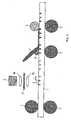
- FIGUREshows by way of example a diagrammatic view of a process sequence for the production of a conductor track and/or an electrode.
- the substrate 1is drawn through between a plurality of rollers for example in a roll-to-roll process. Shown from left to right are firstly the pressing and/or guide rollers 2 which promote a uniform travel movement of the strip.
- recesses 5are then produced in the substrate with a laser 3 , for example an excimer laser, through a mask 4 .
- the excimer laser 3is possibly provided with optical lens systems 3 a, 3 b so that the recesses 5 are not necessarily imaged in the same size as predetermined by the mask 4 .
- the laser pulselasts for example only a few 10 ns, the strip 1 has advanced only insignificantly in time.
- the recesses 5 produced in that wayhave sharp edges, steep walls and a rough bottom surface to which the organic conductors particularly firmly adhere.
- organic electrically conductive material 6such as for example PANI (polyaniline) or PEDOT in solution or in the form of a paste is scraped into the recesses.
- Any conductive material 6 which may be present between the recessesis then removed with an absorbent roller 8 .
- the roller 8rotates for example more slowly than the other rollers so that the material is effectively wiped off.
- the spacing between two recesses 5is identified by the double-headed arrow and is denoted by I.
- organic polymeror ‘functional material’ or ‘(functional) polymer’ here embraces all kinds of organic, metallorganic and/or organic-inorganic plastic materials (hybrids), in particular those which are identified in English for example by ‘plastics’. This involves all kinds of substances with the exception of the semiconductors which form the conventional diodes (germanium, silicon) and the typical metallic conductors. Restriction in a dogmatic sense to organic material as carbon-bearing material is accordingly not intended, but rather the broad use of for example silicones is also envisaged. In addition the term is not to be subjected to any restriction in regard to the molecule size, in particular to polymeric and/or oligomeric materials, but the use of small molecules is certainly also possible.
- the word component ‘polymer’ in the expression functional polymeris historically governed and in that respect does not make any statement about the presence of an actually polymeric bond.
- the inventionfor the first time provides a process with which an organic electronic component such as an OFET with a high switching speed and a high level of reliability can be economically produced. It has been found that recesses which are burnt in with a laser hold the filling with conductive organic material differently from the conventional recesses and that therefore organic conductor tracks can be produced more quickly and better with this method than with other methods.
Landscapes
- Engineering & Computer Science (AREA)
- Manufacturing & Machinery (AREA)
- Electrodes Of Semiconductors (AREA)
- Thin Film Transistor (AREA)
- Liquid Deposition Of Substances Of Which Semiconductor Devices Are Composed (AREA)
- Internal Circuitry In Semiconductor Integrated Circuit Devices (AREA)
Abstract
Description
- The invention concerns an organic electronic component with high-resolution structuring, in particular an organic field effect transistor (OFET) with a small source-drain spacing, and a process for the production thereof.
- Organic electronic components are known, in particular OFETs with high-resolution structuring and a small source-drain spacing ‘I’; but they are produced using expensive process steps which entail high cost levels. Those process steps are uneconomical and usually include photolithography, wherein recesses are produced in a lower layer or in the substrate by photolithographic means so that a conductor track with the required capacitance can be formed. Those recesses are trough-shaped and do not involve sharp contours. The bottom of the recesses remains unchanged.
- A conductor track and/or an electrode needs a certain mass in order to have a low resistance, which is best disposed in a 1-2 μm recess. Hitherto however there is no process which, in a quick and inexpensive production procedure, produces the conductor tracks/electrodes of an OFET in that way.
- The known processes for producing organic electronic components, which are quick and suitable for mass production, make use of the technology of applying the conductor track to the lower layer, generally therefore to the substrate, in which case the problem which arises is that those ‘superposed’ conductor tracks are either so thick that they cause defect locations in the subsequent insulating layer or layers, or they are so wide that a large part of the overall surface area of the integrated circuit is used for same.
- Admittedly, DE 10061297.0 discloses a high-resolution printing process which can be used on a large technological scale and in which the conductor tracks are recessed, but it suffers from the disadvantage that the recesses which are produced by impressing thereon with an embossing stamp do not have steep wall surfaces and sharply defined edges but are more trough-shaped and do not have sharp contours. As a consequence of those gentle transitions, the material introduced into the recess does not accurately fill only the recess, but it smears and smudges around the recess and thus leads to leakage currents. The smeared material also cannot be subsequently wiped off, without wiping a large part of the material out of the recess again.
- The object of the invention is to provide an organic electronic component which can be produced on a large technological scale and favourably, in particular an OFET with a high-resolution structure and a small source-drain spacing.
- The way in which that object is attained and the subject-matter of the invention is an organic electronic component with a spacing I between two conductor tracks, electrodes and/or between a conductor track and an electrode of less than 10 μm, which has a substantially flat surface, that is to say the conductor track or tracks and/or the electrode or electrodes are raised less than 300 nm above the surface of a lower layer or the substrate. The subject-matter of the invention is also an organic electronic component with a spacing I between two conductor tracks, electrodes and/or between a conductor track and an electrode of less than 10 μm, wherein at least one conductor track and/or electrode is arranged in a recess of a lower layer, wherein the recess was produced by means of a layer, that is to say it has steep walls, sharp contours and a relatively rough bottom surface.
- Finally the subject-matter of the invention is a process for the production of an organic electronic component in which to produce a conductor track and/or an electrode at least one recess is burnt into a lower layer or the substrate by means of laser and mask, wherein said recess has steep walls, sharp contours and a rough surface at the bottom, and in a subsequent process step is filled with conductive, predominantly organic material.
- In accordance with an embodiment of the process, in a process step following the step of filling the recesses with said conductive organic material, excess conductive organic material is wiped away without in that case conductive material being removed from the recess to a noticeable extent again.
- The recesses can be filled using various procedures: the material can be sprayed, scraped in by a blade, injected, applied by coating, applied by printing or introduced into the recesses in any other manner according to the invention.
- In accordance with an embodiment of the process the recesses are burnt into the lower layer and/or the substrate with a pulsed layer, for example with pulse lengths of some 10 ns. In that case a few pulses can already suffice to produce recesses in the region of between 0.5 and 382 m.
- The recesses produced by laser structuring are distinguished in that the walls are very steep and in the extreme case directly perpendicular. In addition the vaporisation effect produces a very rough surface at the bottom of the recesses, which has the consequence that the organic conductor introduced has very good adhesion there and is not sucked out of and/or removed from the recesses to any extent worth mentioning, by virtue of the operation of removing the excess conductive material between the recesses. In that way, the recesses which are burnt in with laser are also clearly distinguished from the recesses which are produced for example by embossing, where the excess organic material which is distributed around the recess cannot be wiped away without involving serious losses.
- The invention is described in greater detail hereinafter with reference to a FIGURE which shows by way of example a diagrammatic view of a process sequence for the production of a conductor track and/or an electrode.
- The
substrate 1 is drawn through between a plurality of rollers for example in a roll-to-roll process. Shown from left to right are firstly the pressing and/orguide rollers 2 which promote a uniform travel movement of the strip. In the first working operation illustrated,recesses 5 are then produced in the substrate with alaser 3, for example an excimer laser, through amask 4. Theexcimer laser 3 is possibly provided withoptical lens systems recesses 5 are not necessarily imaged in the same size as predetermined by themask 4. As the laser pulse lasts for example only a few 10 ns, thestrip 1 has advanced only insignificantly in time. As described above, therecesses 5 produced in that way have sharp edges, steep walls and a rough bottom surface to which the organic conductors particularly firmly adhere. Then, using a doctor blade7, organic electricallyconductive material 6 such as for example PANI (polyaniline) or PEDOT in solution or in the form of a paste is scraped into the recesses. Anyconductive material 6 which may be present between the recesses is then removed with anabsorbent roller 8. Theroller 8 rotates for example more slowly than the other rollers so that the material is effectively wiped off. The spacing between tworecesses 5 is identified by the double-headed arrow and is denoted by I. - The term ‘organic polymer’ or ‘functional material’ or ‘(functional) polymer’ here embraces all kinds of organic, metallorganic and/or organic-inorganic plastic materials (hybrids), in particular those which are identified in English for example by ‘plastics’. This involves all kinds of substances with the exception of the semiconductors which form the conventional diodes (germanium, silicon) and the typical metallic conductors. Restriction in a dogmatic sense to organic material as carbon-bearing material is accordingly not intended, but rather the broad use of for example silicones is also envisaged. In addition the term is not to be subjected to any restriction in regard to the molecule size, in particular to polymeric and/or oligomeric materials, but the use of small molecules is certainly also possible. The word component ‘polymer’ in the expression functional polymer is historically governed and in that respect does not make any statement about the presence of an actually polymeric bond.
- The invention for the first time provides a process with which an organic electronic component such as an OFET with a high switching speed and a high level of reliability can be economically produced. It has been found that recesses which are burnt in with a laser hold the filling with conductive organic material differently from the conventional recesses and that therefore organic conductor tracks can be produced more quickly and better with this method than with other methods.
Claims (8)
1. An organic electronic component including a lower layer having a top surface with a spacing I between two adjacent conductor tracks, two adjacent electrodes and/or between a conductor track and an electrode of less than 10 μm in the lower layer, wherein at least one conductor track and/or electrode is arranged in a recess of the lower layer, wherein the recess is produced by a laser, the recess having relatively steep side walls generally perpendicular to the top surface and a bottom surface, the recess exhibiting relatively sharp contours at the junction of the side walls with the bottom recess surface and with the lower layer top surface and a relatively rough bottom surface as compared to the top surface of the lower layer.
2. A process for the production of an organic electronic component including a substrate or lower layer having a top surface, the process for producing a conductor track and/or an electrode in the substrate or lower layer by burning at least one recess into the lower layer or into the substrate by emitting a laser beam through a mask, wherein said recess has a bottom surface and relatively steep walls relative to the top surface, the recess exhibiting relatively sharp contours between the side walls and bottom surface and between the side walls and the top surface and a rough surface at the bottom surface as compared to the top surface, and then filling the recess in a subsequent process step with conductive, predominantly organic material.
3. A process as set for the inclaim 2 wherein the conductive material is scraped into the recess.
4. A process as set forth in one of claims2 and3 wherein excess conductive organic material is wiped away in a process step following the step of filling the recess with said material.
5. A process as set forth in one of claims2 through3 wherein the laser is pulsed.
6. A process as set forth in one of claims2 through3 which is performed in a continuous roll-to-roll procedure.
7. A process as set forth inclaim 6 wherein the roll-to-roll procedure including pressing or guiding the substrate or lower layer with pressing or guide rollers and wiping off the excess organic material from the top surface with a wiping roller, the wiping roller rotating more slowly than the pressing or guide rollers.
8. The process as set forth in one of claims2 and3 wherein the laser is an excimer laser.
Applications Claiming Priority (3)
| Application Number | Priority Date | Filing Date | Title |
|---|---|---|---|
| DE10251475 | 2002-11-05 | ||
| DE10251475.5 | 2002-11-05 | ||
| PCT/DE2003/003667WO2004042837A2 (en) | 2002-11-05 | 2003-11-05 | Organic electronic component with high-resolution structuring and method for the production thereof |
Publications (1)
| Publication Number | Publication Date |
|---|---|
| US20060118778A1true US20060118778A1 (en) | 2006-06-08 |
Family
ID=32308476
Family Applications (1)
| Application Number | Title | Priority Date | Filing Date |
|---|---|---|---|
| US10/533,756AbandonedUS20060118778A1 (en) | 2002-11-05 | 2003-11-05 | Organic electronic component with high-resolution structuring and method for the production thereof |
Country Status (5)
| Country | Link |
|---|---|
| US (1) | US20060118778A1 (en) |
| EP (1) | EP1559148A2 (en) |
| JP (1) | JP2006505927A (en) |
| CN (1) | CN1726604A (en) |
| WO (1) | WO2004042837A2 (en) |
Cited By (1)
| Publication number | Priority date | Publication date | Assignee | Title |
|---|---|---|---|---|
| US20080175996A1 (en)* | 2007-01-23 | 2008-07-24 | Commissariat A L'energie Atomique | Method for depositing a polymer layer on a surface of a support comprising at least a recessed zone |
Families Citing this family (27)
| Publication number | Priority date | Publication date | Assignee | Title |
|---|---|---|---|---|
| US7875975B2 (en) | 2000-08-18 | 2011-01-25 | Polyic Gmbh & Co. Kg | Organic integrated circuit completely encapsulated by multi-layered barrier and included in RFID tag |
| DE10043204A1 (en) | 2000-09-01 | 2002-04-04 | Siemens Ag | Organic field-effect transistor, method for structuring an OFET and integrated circuit |
| DE10061299A1 (en) | 2000-12-08 | 2002-06-27 | Siemens Ag | Device for determining and / or forwarding at least one environmental influence, production method and use thereof |
| DE10061297C2 (en) | 2000-12-08 | 2003-05-28 | Siemens Ag | Procedure for structuring an OFET |
| DE10105914C1 (en) | 2001-02-09 | 2002-10-10 | Siemens Ag | Organic field effect transistor with photo-structured gate dielectric and a method for its production |
| DE10151036A1 (en) | 2001-10-16 | 2003-05-08 | Siemens Ag | Isolator for an organic electronic component |
| DE10151440C1 (en) | 2001-10-18 | 2003-02-06 | Siemens Ag | Organic electronic component for implementing an encapsulated partially organic electronic component has components like a flexible foil as an antenna, a diode or capacitor and an organic transistor. |
| DE10160732A1 (en) | 2001-12-11 | 2003-06-26 | Siemens Ag | OFET used e.g. in RFID tag, comprises an intermediate layer on an active semiconductor layer |
| DE10212640B4 (en) | 2002-03-21 | 2004-02-05 | Siemens Ag | Logical components made of organic field effect transistors |
| US8044517B2 (en) | 2002-07-29 | 2011-10-25 | Polyic Gmbh & Co. Kg | Electronic component comprising predominantly organic functional materials and a method for the production thereof |
| DE50306683D1 (en) | 2002-08-23 | 2007-04-12 | Polyic Gmbh & Co Kg | ORGANIC COMPONENT FOR OVERVOLTAGE PROTECTION AND ASSOCIATED CIRCUIT |
| DE10253154A1 (en) | 2002-11-14 | 2004-05-27 | Siemens Ag | Biosensor, used to identify analyte in liquid sample, has test field with detector, where detector registers field changes as electrical signals for evaluation |
| EP1563553B1 (en) | 2002-11-19 | 2007-02-14 | PolyIC GmbH & Co. KG | Organic electronic circuitcomprising a structured, semi-conductive functional layer and a method for producing said component |
| DE10302149A1 (en) | 2003-01-21 | 2005-08-25 | Siemens Ag | Use of conductive carbon black / graphite blends for the production of low-cost electronics |
| DE10339036A1 (en) | 2003-08-25 | 2005-03-31 | Siemens Ag | Organic electronic component with high-resolution structuring and manufacturing method |
| DE10340643B4 (en) | 2003-09-03 | 2009-04-16 | Polyic Gmbh & Co. Kg | Printing method for producing a double layer for polymer electronics circuits, and thereby produced electronic component with double layer |
| DE10340644B4 (en) | 2003-09-03 | 2010-10-07 | Polyic Gmbh & Co. Kg | Mechanical controls for organic polymer electronics |
| DE102004040831A1 (en) | 2004-08-23 | 2006-03-09 | Polyic Gmbh & Co. Kg | Radio-tag compatible outer packaging |
| DE102004059465A1 (en) | 2004-12-10 | 2006-06-14 | Polyic Gmbh & Co. Kg | recognition system |
| DE102004059464A1 (en) | 2004-12-10 | 2006-06-29 | Polyic Gmbh & Co. Kg | Electronic component with modulator |
| DE102004063435A1 (en) | 2004-12-23 | 2006-07-27 | Polyic Gmbh & Co. Kg | Organic rectifier |
| DE102005009819A1 (en) | 2005-03-01 | 2006-09-07 | Polyic Gmbh & Co. Kg | electronics assembly |
| DE102005009820A1 (en) | 2005-03-01 | 2006-09-07 | Polyic Gmbh & Co. Kg | Electronic assembly with organic logic switching elements |
| DE102005017655B4 (en) | 2005-04-15 | 2008-12-11 | Polyic Gmbh & Co. Kg | Multilayer composite body with electronic function |
| DE102005031448A1 (en) | 2005-07-04 | 2007-01-11 | Polyic Gmbh & Co. Kg | Activatable optical layer |
| DE102005035589A1 (en) | 2005-07-29 | 2007-02-01 | Polyic Gmbh & Co. Kg | Manufacturing electronic component on surface of substrate where component has two overlapping function layers |
| US8134233B2 (en) | 2007-07-30 | 2012-03-13 | Motorola Solutions, Inc. | Method and apparatus for providing electrically isolated closely spaced features on a printed circuit board |
Citations (91)
| Publication number | Priority date | Publication date | Assignee | Title |
|---|---|---|---|---|
| US3512052A (en)* | 1968-01-11 | 1970-05-12 | Gen Motors Corp | Metal-insulator-semiconductor voltage variable capacitor with controlled resistivity dielectric |
| US3769096A (en)* | 1971-03-12 | 1973-10-30 | Bell Telephone Labor Inc | Pyroelectric devices |
| US3955098A (en)* | 1973-10-12 | 1976-05-04 | Hitachi, Ltd. | Switching circuit having floating gate mis load transistors |
| US4302648A (en)* | 1978-01-26 | 1981-11-24 | Shin-Etsu Polymer Co., Ltd. | Key-board switch unit |
| US4340657A (en)* | 1980-02-19 | 1982-07-20 | Polychrome Corporation | Novel radiation-sensitive articles |
| US4442019A (en)* | 1978-05-26 | 1984-04-10 | Marks Alvin M | Electroordered dipole suspension |
| US4865197A (en)* | 1988-03-04 | 1989-09-12 | Unisys Corporation | Electronic component transportation container |
| US4926052A (en)* | 1986-03-03 | 1990-05-15 | Kabushiki Kaisha Toshiba | Radiation detecting device |
| US4937119A (en)* | 1988-12-15 | 1990-06-26 | Hoechst Celanese Corp. | Textured organic optical data storage media and methods of preparation |
| US5173835A (en)* | 1991-10-15 | 1992-12-22 | Motorola, Inc. | Voltage variable capacitor |
| US5206525A (en)* | 1989-12-27 | 1993-04-27 | Nippon Petrochemicals Co., Ltd. | Electric element capable of controlling the electric conductivity of π-conjugated macromolecular materials |
| US5259926A (en)* | 1991-09-24 | 1993-11-09 | Hitachi, Ltd. | Method of manufacturing a thin-film pattern on a substrate |
| US5321240A (en)* | 1992-01-30 | 1994-06-14 | Mitsubishi Denki Kabushiki Kaisha | Non-contact IC card |
| US5347144A (en)* | 1990-07-04 | 1994-09-13 | Centre National De La Recherche Scientifique (Cnrs) | Thin-layer field-effect transistors with MIS structure whose insulator and semiconductor are made of organic materials |
| US5364735A (en)* | 1988-07-01 | 1994-11-15 | Sony Corporation | Multiple layer optical record medium with protective layers and method for producing same |
| US5395504A (en)* | 1993-02-04 | 1995-03-07 | Asulab S.A. | Electrochemical measuring system with multizone sensors |
| US5480839A (en)* | 1993-01-15 | 1996-01-02 | Kabushiki Kaisha Toshiba | Semiconductor device manufacturing method |
| US5486851A (en)* | 1991-10-30 | 1996-01-23 | Fraunhofer-Gesellschaft Zur Forderung Der Angewandten Forschung E.V. | Illumination device using a pulsed laser source a Schlieren optical system and a matrix addressable surface light modulator for producing images with undifracted light |
| US5494781A (en)* | 1993-08-26 | 1996-02-27 | Matsushita Electric Works, Ltd. | Method for manufacturing printed circuit board |
| US5502396A (en)* | 1993-09-21 | 1996-03-26 | Asulab S.A. | Measuring device with connection for a removable sensor |
| US5546889A (en)* | 1993-10-06 | 1996-08-20 | Matsushita Electric Industrial Co., Ltd. | Method of manufacturing organic oriented film and method of manufacturing electronic device |
| US5569879A (en)* | 1991-02-19 | 1996-10-29 | Gemplus Card International | Integrated circuit micromodule obtained by the continuous assembly of patterned strips |
| US5574291A (en)* | 1994-12-09 | 1996-11-12 | Lucent Technologies Inc. | Article comprising a thin film transistor with low conductivity organic layer |
| US5578513A (en)* | 1993-09-17 | 1996-11-26 | Mitsubishi Denki Kabushiki Kaisha | Method of making a semiconductor device having a gate all around type of thin film transistor |
| US5580794A (en)* | 1993-08-24 | 1996-12-03 | Metrika Laboratories, Inc. | Disposable electronic assay device |
| US5625199A (en)* | 1996-01-16 | 1997-04-29 | Lucent Technologies Inc. | Article comprising complementary circuit with inorganic n-channel and organic p-channel thin film transistors |
| US5629530A (en)* | 1994-05-16 | 1997-05-13 | U.S. Phillips Corporation | Semiconductor device having an organic semiconductor material |
| US5630986A (en)* | 1995-01-13 | 1997-05-20 | Bayer Corporation | Dispensing instrument for fluid monitoring sensors |
| US5652645A (en)* | 1995-07-24 | 1997-07-29 | Anvik Corporation | High-throughput, high-resolution, projection patterning system for large, flexible, roll-fed, electronic-module substrates |
| US5691089A (en)* | 1993-03-25 | 1997-11-25 | Texas Instruments Incorporated | Integrated circuits formed in radiation sensitive material and method of forming same |
| US5705826A (en)* | 1994-06-28 | 1998-01-06 | Hitachi, Ltd. | Field-effect transistor having a semiconductor layer made of an organic compound |
| US5729428A (en)* | 1995-04-25 | 1998-03-17 | Nec Corporation | Solid electrolytic capacitor with conductive polymer as solid electrolyte and method for fabricating the same |
| US5869972A (en)* | 1996-02-26 | 1999-02-09 | Birch; Brian Jeffrey | Testing device using a thermochromic display and method of using same |
| US5883397A (en)* | 1993-07-01 | 1999-03-16 | Mitsubishi Denki Kabushiki Kaisha | Plastic functional element |
| US5892244A (en)* | 1989-01-10 | 1999-04-06 | Mitsubishi Denki Kabushiki Kaisha | Field effect transistor including πconjugate polymer and liquid crystal display including the field effect transistor |
| US5946551A (en)* | 1997-03-25 | 1999-08-31 | Dimitrakopoulos; Christos Dimitrios | Fabrication of thin film effect transistor comprising an organic semiconductor and chemical solution deposited metal oxide gate dielectric |
| US5970318A (en)* | 1997-05-15 | 1999-10-19 | Electronics And Telecommunications Research Institute | Fabrication method of an organic electroluminescent devices |
| US5967048A (en)* | 1998-06-12 | 1999-10-19 | Howard A. Fromson | Method and apparatus for the multiple imaging of a continuous web |
| US5973598A (en)* | 1997-09-11 | 1999-10-26 | Precision Dynamics Corporation | Radio frequency identification tag on flexible substrate |
| US5997817A (en)* | 1997-12-05 | 1999-12-07 | Roche Diagnostics Corporation | Electrochemical biosensor test strip |
| US5998805A (en)* | 1997-12-11 | 1999-12-07 | Motorola, Inc. | Active matrix OED array with improved OED cathode |
| US6036919A (en)* | 1996-07-23 | 2000-03-14 | Roche Diagnostic Gmbh | Diagnostic test carrier with multilayer field |
| US6045977A (en)* | 1998-02-19 | 2000-04-04 | Lucent Technologies Inc. | Process for patterning conductive polyaniline films |
| US6087196A (en)* | 1998-01-30 | 2000-07-11 | The Trustees Of Princeton University | Fabrication of organic semiconductor devices using ink jet printing |
| US6133835A (en)* | 1997-12-05 | 2000-10-17 | U.S. Philips Corporation | Identification transponder |
| US6150668A (en)* | 1998-05-29 | 2000-11-21 | Lucent Technologies Inc. | Thin-film transistor monolithically integrated with an organic light-emitting diode |
| US6197663B1 (en)* | 1999-12-07 | 2001-03-06 | Lucent Technologies Inc. | Process for fabricating integrated circuit devices having thin film transistors |
| US6207472B1 (en)* | 1999-03-09 | 2001-03-27 | International Business Machines Corporation | Low temperature thin film transistor fabrication |
| US6215130B1 (en)* | 1998-08-20 | 2001-04-10 | Lucent Technologies Inc. | Thin film transistors |
| US6221553B1 (en)* | 1999-01-15 | 2001-04-24 | 3M Innovative Properties Company | Thermal transfer element for forming multilayer devices |
| US6251513B1 (en)* | 1997-11-08 | 2001-06-26 | Littlefuse, Inc. | Polymer composites for overvoltage protection |
| US6284562B1 (en)* | 1999-11-17 | 2001-09-04 | Agere Systems Guardian Corp. | Thin film transistors |
| US6300141B1 (en)* | 1999-03-02 | 2001-10-09 | Helix Biopharma Corporation | Card-based biosensor device |
| US6322736B1 (en)* | 1998-03-27 | 2001-11-27 | Agere Systems Inc. | Method for fabricating molded microstructures on substrates |
| US6321571B1 (en)* | 1998-12-21 | 2001-11-27 | Corning Incorporated | Method of making glass structures for flat panel displays |
| US6330464B1 (en)* | 1998-08-26 | 2001-12-11 | Sensors For Medicine & Science | Optical-based sensing devices |
| US6329226B1 (en)* | 2000-06-01 | 2001-12-11 | Agere Systems Guardian Corp. | Method for fabricating a thin-film transistor |
| US6335539B1 (en)* | 1999-11-05 | 2002-01-01 | International Business Machines Corporation | Method for improving performance of organic semiconductors in bottom electrode structure |
| US6340822B1 (en)* | 1999-10-05 | 2002-01-22 | Agere Systems Guardian Corp. | Article comprising vertically nano-interconnected circuit devices and method for making the same |
| US6344662B1 (en)* | 1997-03-25 | 2002-02-05 | International Business Machines Corporation | Thin-film field-effect transistor with organic-inorganic hybrid semiconductor requiring low operating voltages |
| US20020018911A1 (en)* | 1999-05-11 | 2002-02-14 | Mark T. Bernius | Electroluminescent or photocell device having protective packaging |
| US20020022284A1 (en)* | 1991-02-27 | 2002-02-21 | Alan J. Heeger | Visible light emitting diodes fabricated from soluble semiconducting polymers |
| US20020025391A1 (en)* | 1989-05-26 | 2002-02-28 | Marie Angelopoulos | Patterns of electrically conducting polymers and their application as electrodes or electrical contacts |
| US6362509B1 (en)* | 1999-10-11 | 2002-03-26 | U.S. Philips Electronics | Field effect transistor with organic semiconductor layer |
| US6384804B1 (en)* | 1998-11-25 | 2002-05-07 | Lucent Techonologies Inc. | Display comprising organic smart pixels |
| US20020053320A1 (en)* | 1998-12-15 | 2002-05-09 | Gregg M. Duthaler | Method for printing of transistor arrays on plastic substrates |
| US20020056839A1 (en)* | 2000-11-11 | 2002-05-16 | Pt Plus Co. Ltd. | Method of crystallizing a silicon thin film and semiconductor device fabricated thereby |
| US20020068392A1 (en)* | 2000-12-01 | 2002-06-06 | Pt Plus Co. Ltd. | Method for fabricating thin film transistor including crystalline silicon active layer |
| US6403396B1 (en)* | 1998-01-28 | 2002-06-11 | Thin Film Electronics Asa | Method for generation of electrically conducting or semiconducting structures in three dimensions and methods for erasure of the same structures |
| US6429450B1 (en)* | 1997-08-22 | 2002-08-06 | Koninklijke Philips Electronics N.V. | Method of manufacturing a field-effect transistor substantially consisting of organic materials |
| US20020130042A1 (en)* | 2000-03-02 | 2002-09-19 | Moerman Piet H.C. | Combined lancet and electrochemical analyte-testing apparatus |
| US20020170897A1 (en)* | 2001-05-21 | 2002-11-21 | Hall Frank L. | Methods for preparing ball grid array substrates via use of a laser |
| US6498114B1 (en)* | 1999-04-09 | 2002-12-24 | E Ink Corporation | Method for forming a patterned semiconductor film |
| US20020195644A1 (en)* | 2001-06-08 | 2002-12-26 | Ananth Dodabalapur | Organic polarizable gate transistor apparatus and method |
| US6517955B1 (en)* | 1999-02-22 | 2003-02-11 | Nippon Steel Corporation | High strength galvanized steel plate excellent in adhesion of plated metal and formability in press working and high strength alloy galvanized steel plate and method for production thereof |
| US20030059987A1 (en)* | 1999-12-21 | 2003-03-27 | Plastic Logic Limited | Inkjet-fabricated integrated circuits |
| US6555840B1 (en)* | 1999-02-16 | 2003-04-29 | Sharp Kabushiki Kaisha | Charge-transport structures |
| US20030112576A1 (en)* | 2001-09-28 | 2003-06-19 | Brewer Peter D. | Process for producing high performance interconnects |
| US6593690B1 (en)* | 1999-09-03 | 2003-07-15 | 3M Innovative Properties Company | Large area organic electronic devices having conducting polymer buffer layers and methods of making same |
| US20030141807A1 (en)* | 2001-01-31 | 2003-07-31 | Takeo Kawase | Display device |
| US6603139B1 (en)* | 1998-04-16 | 2003-08-05 | Cambridge Display Technology Limited | Polymer devices |
| US6621098B1 (en)* | 1999-11-29 | 2003-09-16 | The Penn State Research Foundation | Thin-film transistor and methods of manufacturing and incorporating a semiconducting organic material |
| US20030175427A1 (en)* | 2002-03-15 | 2003-09-18 | Yeuh-Lin Loo | Forming nanoscale patterned thin film metal layers |
| US20040002176A1 (en)* | 2002-06-28 | 2004-01-01 | Xerox Corporation | Organic ferroelectric memory cells |
| US20040013982A1 (en)* | 1999-09-14 | 2004-01-22 | Massachusetts Institute Of Technology | Fabrication of finely featured devices by liquid embossing |
| US20040026689A1 (en)* | 2000-08-18 | 2004-02-12 | Adolf Bernds | Encapsulated organic-electronic component, method for producing the same and use thereof |
| US20040084670A1 (en)* | 2002-11-04 | 2004-05-06 | Tripsas Nicholas H. | Stacked organic memory devices and methods of operating and fabricating |
| US20040211329A1 (en)* | 2001-09-18 | 2004-10-28 | Katsuyuki Funahata | Pattern forming method and pattern forming device |
| US6852583B2 (en)* | 2000-07-07 | 2005-02-08 | Siemens Aktiengesellschaft | Method for the production and configuration of organic field-effect transistors (OFET) |
| US6903958B2 (en)* | 2000-09-13 | 2005-06-07 | Siemens Aktiengesellschaft | Method of writing to an organic memory |
| US7229868B2 (en)* | 2000-12-08 | 2007-06-12 | Polyic Gmbh & Co. Kg | Organic field-effect transistor, method for structuring an OFET and integrated circuit |
Family Cites Families (4)
| Publication number | Priority date | Publication date | Assignee | Title |
|---|---|---|---|---|
| KR100282393B1 (en)* | 1998-06-17 | 2001-02-15 | 구자홍 | method for fabricating Organic Electroluminescent display Device |
| US6867539B1 (en)* | 2000-07-12 | 2005-03-15 | 3M Innovative Properties Company | Encapsulated organic electronic devices and method for making same |
| US6767807B2 (en)* | 2001-03-02 | 2004-07-27 | Fuji Photo Film Co., Ltd. | Method for producing organic thin film device and transfer material used therein |
| DE10219905B4 (en)* | 2002-05-03 | 2011-06-22 | OSRAM Opto Semiconductors GmbH, 93055 | Optoelectronic component with organic functional layers and two carriers and method for producing such an optoelectronic component |
- 2003
- 2003-11-05JPJP2004549084Apatent/JP2006505927A/enactivePending
- 2003-11-05CNCNA2003801059676Apatent/CN1726604A/enactivePending
- 2003-11-05USUS10/533,756patent/US20060118778A1/ennot_activeAbandoned
- 2003-11-05WOPCT/DE2003/003667patent/WO2004042837A2/enactiveApplication Filing
- 2003-11-05EPEP03785493Apatent/EP1559148A2/ennot_activeWithdrawn
Patent Citations (93)
| Publication number | Priority date | Publication date | Assignee | Title |
|---|---|---|---|---|
| US3512052A (en)* | 1968-01-11 | 1970-05-12 | Gen Motors Corp | Metal-insulator-semiconductor voltage variable capacitor with controlled resistivity dielectric |
| US3769096A (en)* | 1971-03-12 | 1973-10-30 | Bell Telephone Labor Inc | Pyroelectric devices |
| US3955098A (en)* | 1973-10-12 | 1976-05-04 | Hitachi, Ltd. | Switching circuit having floating gate mis load transistors |
| US4302648A (en)* | 1978-01-26 | 1981-11-24 | Shin-Etsu Polymer Co., Ltd. | Key-board switch unit |
| US4442019A (en)* | 1978-05-26 | 1984-04-10 | Marks Alvin M | Electroordered dipole suspension |
| US4340657A (en)* | 1980-02-19 | 1982-07-20 | Polychrome Corporation | Novel radiation-sensitive articles |
| US4926052A (en)* | 1986-03-03 | 1990-05-15 | Kabushiki Kaisha Toshiba | Radiation detecting device |
| US4865197A (en)* | 1988-03-04 | 1989-09-12 | Unisys Corporation | Electronic component transportation container |
| US5364735A (en)* | 1988-07-01 | 1994-11-15 | Sony Corporation | Multiple layer optical record medium with protective layers and method for producing same |
| US4937119A (en)* | 1988-12-15 | 1990-06-26 | Hoechst Celanese Corp. | Textured organic optical data storage media and methods of preparation |
| US6060338A (en)* | 1989-01-10 | 2000-05-09 | Mitsubishi Denki Kabushiki Kaisha | Method of making a field effect transistor |
| US5892244A (en)* | 1989-01-10 | 1999-04-06 | Mitsubishi Denki Kabushiki Kaisha | Field effect transistor including πconjugate polymer and liquid crystal display including the field effect transistor |
| US20020025391A1 (en)* | 1989-05-26 | 2002-02-28 | Marie Angelopoulos | Patterns of electrically conducting polymers and their application as electrodes or electrical contacts |
| US5206525A (en)* | 1989-12-27 | 1993-04-27 | Nippon Petrochemicals Co., Ltd. | Electric element capable of controlling the electric conductivity of π-conjugated macromolecular materials |
| US5347144A (en)* | 1990-07-04 | 1994-09-13 | Centre National De La Recherche Scientifique (Cnrs) | Thin-layer field-effect transistors with MIS structure whose insulator and semiconductor are made of organic materials |
| US5569879A (en)* | 1991-02-19 | 1996-10-29 | Gemplus Card International | Integrated circuit micromodule obtained by the continuous assembly of patterned strips |
| US20020022284A1 (en)* | 1991-02-27 | 2002-02-21 | Alan J. Heeger | Visible light emitting diodes fabricated from soluble semiconducting polymers |
| US5259926A (en)* | 1991-09-24 | 1993-11-09 | Hitachi, Ltd. | Method of manufacturing a thin-film pattern on a substrate |
| US5173835A (en)* | 1991-10-15 | 1992-12-22 | Motorola, Inc. | Voltage variable capacitor |
| US5486851A (en)* | 1991-10-30 | 1996-01-23 | Fraunhofer-Gesellschaft Zur Forderung Der Angewandten Forschung E.V. | Illumination device using a pulsed laser source a Schlieren optical system and a matrix addressable surface light modulator for producing images with undifracted light |
| US5321240A (en)* | 1992-01-30 | 1994-06-14 | Mitsubishi Denki Kabushiki Kaisha | Non-contact IC card |
| US5480839A (en)* | 1993-01-15 | 1996-01-02 | Kabushiki Kaisha Toshiba | Semiconductor device manufacturing method |
| US5395504A (en)* | 1993-02-04 | 1995-03-07 | Asulab S.A. | Electrochemical measuring system with multizone sensors |
| US5691089A (en)* | 1993-03-25 | 1997-11-25 | Texas Instruments Incorporated | Integrated circuits formed in radiation sensitive material and method of forming same |
| US5883397A (en)* | 1993-07-01 | 1999-03-16 | Mitsubishi Denki Kabushiki Kaisha | Plastic functional element |
| US5580794A (en)* | 1993-08-24 | 1996-12-03 | Metrika Laboratories, Inc. | Disposable electronic assay device |
| US5494781A (en)* | 1993-08-26 | 1996-02-27 | Matsushita Electric Works, Ltd. | Method for manufacturing printed circuit board |
| US5578513A (en)* | 1993-09-17 | 1996-11-26 | Mitsubishi Denki Kabushiki Kaisha | Method of making a semiconductor device having a gate all around type of thin film transistor |
| US5502396A (en)* | 1993-09-21 | 1996-03-26 | Asulab S.A. | Measuring device with connection for a removable sensor |
| US5546889A (en)* | 1993-10-06 | 1996-08-20 | Matsushita Electric Industrial Co., Ltd. | Method of manufacturing organic oriented film and method of manufacturing electronic device |
| US5629530A (en)* | 1994-05-16 | 1997-05-13 | U.S. Phillips Corporation | Semiconductor device having an organic semiconductor material |
| US5705826A (en)* | 1994-06-28 | 1998-01-06 | Hitachi, Ltd. | Field-effect transistor having a semiconductor layer made of an organic compound |
| US5854139A (en)* | 1994-06-28 | 1998-12-29 | Hitachi, Ltd. | Organic field-effect transistor and production thereof |
| US5574291A (en)* | 1994-12-09 | 1996-11-12 | Lucent Technologies Inc. | Article comprising a thin film transistor with low conductivity organic layer |
| US5630986A (en)* | 1995-01-13 | 1997-05-20 | Bayer Corporation | Dispensing instrument for fluid monitoring sensors |
| US5729428A (en)* | 1995-04-25 | 1998-03-17 | Nec Corporation | Solid electrolytic capacitor with conductive polymer as solid electrolyte and method for fabricating the same |
| US5652645A (en)* | 1995-07-24 | 1997-07-29 | Anvik Corporation | High-throughput, high-resolution, projection patterning system for large, flexible, roll-fed, electronic-module substrates |
| US5625199A (en)* | 1996-01-16 | 1997-04-29 | Lucent Technologies Inc. | Article comprising complementary circuit with inorganic n-channel and organic p-channel thin film transistors |
| US5869972A (en)* | 1996-02-26 | 1999-02-09 | Birch; Brian Jeffrey | Testing device using a thermochromic display and method of using same |
| US6036919A (en)* | 1996-07-23 | 2000-03-14 | Roche Diagnostic Gmbh | Diagnostic test carrier with multilayer field |
| US5946551A (en)* | 1997-03-25 | 1999-08-31 | Dimitrakopoulos; Christos Dimitrios | Fabrication of thin film effect transistor comprising an organic semiconductor and chemical solution deposited metal oxide gate dielectric |
| US6344662B1 (en)* | 1997-03-25 | 2002-02-05 | International Business Machines Corporation | Thin-film field-effect transistor with organic-inorganic hybrid semiconductor requiring low operating voltages |
| US5970318A (en)* | 1997-05-15 | 1999-10-19 | Electronics And Telecommunications Research Institute | Fabrication method of an organic electroluminescent devices |
| US6429450B1 (en)* | 1997-08-22 | 2002-08-06 | Koninklijke Philips Electronics N.V. | Method of manufacturing a field-effect transistor substantially consisting of organic materials |
| US5973598A (en)* | 1997-09-11 | 1999-10-26 | Precision Dynamics Corporation | Radio frequency identification tag on flexible substrate |
| US6251513B1 (en)* | 1997-11-08 | 2001-06-26 | Littlefuse, Inc. | Polymer composites for overvoltage protection |
| US6133835A (en)* | 1997-12-05 | 2000-10-17 | U.S. Philips Corporation | Identification transponder |
| US5997817A (en)* | 1997-12-05 | 1999-12-07 | Roche Diagnostics Corporation | Electrochemical biosensor test strip |
| US5998805A (en)* | 1997-12-11 | 1999-12-07 | Motorola, Inc. | Active matrix OED array with improved OED cathode |
| US6403396B1 (en)* | 1998-01-28 | 2002-06-11 | Thin Film Electronics Asa | Method for generation of electrically conducting or semiconducting structures in three dimensions and methods for erasure of the same structures |
| US6087196A (en)* | 1998-01-30 | 2000-07-11 | The Trustees Of Princeton University | Fabrication of organic semiconductor devices using ink jet printing |
| US6045977A (en)* | 1998-02-19 | 2000-04-04 | Lucent Technologies Inc. | Process for patterning conductive polyaniline films |
| US6322736B1 (en)* | 1998-03-27 | 2001-11-27 | Agere Systems Inc. | Method for fabricating molded microstructures on substrates |
| US6603139B1 (en)* | 1998-04-16 | 2003-08-05 | Cambridge Display Technology Limited | Polymer devices |
| US6150668A (en)* | 1998-05-29 | 2000-11-21 | Lucent Technologies Inc. | Thin-film transistor monolithically integrated with an organic light-emitting diode |
| US5967048A (en)* | 1998-06-12 | 1999-10-19 | Howard A. Fromson | Method and apparatus for the multiple imaging of a continuous web |
| US6215130B1 (en)* | 1998-08-20 | 2001-04-10 | Lucent Technologies Inc. | Thin film transistors |
| US6330464B1 (en)* | 1998-08-26 | 2001-12-11 | Sensors For Medicine & Science | Optical-based sensing devices |
| US6384804B1 (en)* | 1998-11-25 | 2002-05-07 | Lucent Techonologies Inc. | Display comprising organic smart pixels |
| US20020053320A1 (en)* | 1998-12-15 | 2002-05-09 | Gregg M. Duthaler | Method for printing of transistor arrays on plastic substrates |
| US6321571B1 (en)* | 1998-12-21 | 2001-11-27 | Corning Incorporated | Method of making glass structures for flat panel displays |
| US6221553B1 (en)* | 1999-01-15 | 2001-04-24 | 3M Innovative Properties Company | Thermal transfer element for forming multilayer devices |
| US6555840B1 (en)* | 1999-02-16 | 2003-04-29 | Sharp Kabushiki Kaisha | Charge-transport structures |
| US6517955B1 (en)* | 1999-02-22 | 2003-02-11 | Nippon Steel Corporation | High strength galvanized steel plate excellent in adhesion of plated metal and formability in press working and high strength alloy galvanized steel plate and method for production thereof |
| US6300141B1 (en)* | 1999-03-02 | 2001-10-09 | Helix Biopharma Corporation | Card-based biosensor device |
| US6207472B1 (en)* | 1999-03-09 | 2001-03-27 | International Business Machines Corporation | Low temperature thin film transistor fabrication |
| US6498114B1 (en)* | 1999-04-09 | 2002-12-24 | E Ink Corporation | Method for forming a patterned semiconductor film |
| US20020018911A1 (en)* | 1999-05-11 | 2002-02-14 | Mark T. Bernius | Electroluminescent or photocell device having protective packaging |
| US6593690B1 (en)* | 1999-09-03 | 2003-07-15 | 3M Innovative Properties Company | Large area organic electronic devices having conducting polymer buffer layers and methods of making same |
| US20040013982A1 (en)* | 1999-09-14 | 2004-01-22 | Massachusetts Institute Of Technology | Fabrication of finely featured devices by liquid embossing |
| US6340822B1 (en)* | 1999-10-05 | 2002-01-22 | Agere Systems Guardian Corp. | Article comprising vertically nano-interconnected circuit devices and method for making the same |
| US6362509B1 (en)* | 1999-10-11 | 2002-03-26 | U.S. Philips Electronics | Field effect transistor with organic semiconductor layer |
| US6335539B1 (en)* | 1999-11-05 | 2002-01-01 | International Business Machines Corporation | Method for improving performance of organic semiconductors in bottom electrode structure |
| US6284562B1 (en)* | 1999-11-17 | 2001-09-04 | Agere Systems Guardian Corp. | Thin film transistors |
| US6621098B1 (en)* | 1999-11-29 | 2003-09-16 | The Penn State Research Foundation | Thin-film transistor and methods of manufacturing and incorporating a semiconducting organic material |
| US6197663B1 (en)* | 1999-12-07 | 2001-03-06 | Lucent Technologies Inc. | Process for fabricating integrated circuit devices having thin film transistors |
| US20030059987A1 (en)* | 1999-12-21 | 2003-03-27 | Plastic Logic Limited | Inkjet-fabricated integrated circuits |
| US20020130042A1 (en)* | 2000-03-02 | 2002-09-19 | Moerman Piet H.C. | Combined lancet and electrochemical analyte-testing apparatus |
| US6329226B1 (en)* | 2000-06-01 | 2001-12-11 | Agere Systems Guardian Corp. | Method for fabricating a thin-film transistor |
| US6852583B2 (en)* | 2000-07-07 | 2005-02-08 | Siemens Aktiengesellschaft | Method for the production and configuration of organic field-effect transistors (OFET) |
| US20040026689A1 (en)* | 2000-08-18 | 2004-02-12 | Adolf Bernds | Encapsulated organic-electronic component, method for producing the same and use thereof |
| US6903958B2 (en)* | 2000-09-13 | 2005-06-07 | Siemens Aktiengesellschaft | Method of writing to an organic memory |
| US20020056839A1 (en)* | 2000-11-11 | 2002-05-16 | Pt Plus Co. Ltd. | Method of crystallizing a silicon thin film and semiconductor device fabricated thereby |
| US20020068392A1 (en)* | 2000-12-01 | 2002-06-06 | Pt Plus Co. Ltd. | Method for fabricating thin film transistor including crystalline silicon active layer |
| US7229868B2 (en)* | 2000-12-08 | 2007-06-12 | Polyic Gmbh & Co. Kg | Organic field-effect transistor, method for structuring an OFET and integrated circuit |
| US20030141807A1 (en)* | 2001-01-31 | 2003-07-31 | Takeo Kawase | Display device |
| US20020170897A1 (en)* | 2001-05-21 | 2002-11-21 | Hall Frank L. | Methods for preparing ball grid array substrates via use of a laser |
| US20020195644A1 (en)* | 2001-06-08 | 2002-12-26 | Ananth Dodabalapur | Organic polarizable gate transistor apparatus and method |
| US20040211329A1 (en)* | 2001-09-18 | 2004-10-28 | Katsuyuki Funahata | Pattern forming method and pattern forming device |
| US20030112576A1 (en)* | 2001-09-28 | 2003-06-19 | Brewer Peter D. | Process for producing high performance interconnects |
| US20030175427A1 (en)* | 2002-03-15 | 2003-09-18 | Yeuh-Lin Loo | Forming nanoscale patterned thin film metal layers |
| US20040002176A1 (en)* | 2002-06-28 | 2004-01-01 | Xerox Corporation | Organic ferroelectric memory cells |
| US20040084670A1 (en)* | 2002-11-04 | 2004-05-06 | Tripsas Nicholas H. | Stacked organic memory devices and methods of operating and fabricating |
Cited By (2)
| Publication number | Priority date | Publication date | Assignee | Title |
|---|---|---|---|---|
| US20080175996A1 (en)* | 2007-01-23 | 2008-07-24 | Commissariat A L'energie Atomique | Method for depositing a polymer layer on a surface of a support comprising at least a recessed zone |
| US8067060B2 (en)* | 2007-01-23 | 2011-11-29 | Commissariat A L'energie Atomique | Method for depositing a polymer layer on a surface of a support comprising at least a recessed zone |
Also Published As
| Publication number | Publication date |
|---|---|
| WO2004042837A3 (en) | 2004-10-07 |
| WO2004042837A2 (en) | 2004-05-21 |
| EP1559148A2 (en) | 2005-08-03 |
| CN1726604A (en) | 2006-01-25 |
| JP2006505927A (en) | 2006-02-16 |
Similar Documents
| Publication | Publication Date | Title |
|---|---|---|
| US20060118778A1 (en) | Organic electronic component with high-resolution structuring and method for the production thereof | |
| KR100804544B1 (en) | Microembossing manufacturing method of electronic device | |
| US7935565B2 (en) | Electronic devices | |
| US8372731B2 (en) | Device fabrication by ink-jet printing materials into bank structures, and embossing tool | |
| DE10140666C2 (en) | Process for producing a conductive structured polymer film and use of the process | |
| KR101392781B1 (en) | METHOD AND APPARATUS FOR FORMING A PATTERNED COATING FILM | |
| EP1487605B1 (en) | Device and method for laser structuring functional polymers and the uses thereof | |
| DE10229118A1 (en) | Process for the inexpensive structuring of conductive polymers by definition of hydrophilic and hydrophobic areas | |
| US7947612B2 (en) | Electronic device array | |
| US6709705B2 (en) | Method of producing a track on a substrate | |
| US7479670B2 (en) | Organic electronic component with high resolution structuring, and method of the production thereof | |
| EP1563720A1 (en) | Method for controlled ink-jet spreading of polymers for the insulation and/or protection of printed circuits | |
| Kang | Gravure-printed Highly-scaled Organic Thin-film Transistors for Low-cost and Large-area Electronics |
Legal Events
| Date | Code | Title | Description |
|---|---|---|---|
| AS | Assignment | Owner name:POLYIC GMBH & CO. KG, GERMANY Free format text:ASSIGNMENT OF ASSIGNORS INTEREST;ASSIGNORS:CLEMENS, WOLFGANG;FIX, WALTER;MANUELLI, ALESSANDRO;AND OTHERS;REEL/FRAME:016551/0190;SIGNING DATES FROM 20050725 TO 20050817 | |
| STCB | Information on status: application discontinuation | Free format text:ABANDONED -- FAILURE TO RESPOND TO AN OFFICE ACTION |