US20060118331A1 - Printed circuit boards for use in optical transceivers - Google Patents
Printed circuit boards for use in optical transceiversDownload PDFInfo
- Publication number
- US20060118331A1 US20060118331A1US11/298,139US29813905AUS2006118331A1US 20060118331 A1US20060118331 A1US 20060118331A1US 29813905 AUS29813905 AUS 29813905AUS 2006118331 A1US2006118331 A1US 2006118331A1
- Authority
- US
- United States
- Prior art keywords
- pcb
- trace
- traces
- optical transceiver
- plated
- Prior art date
- Legal status (The legal status is an assumption and is not a legal conclusion. Google has not performed a legal analysis and makes no representation as to the accuracy of the status listed.)
- Granted
Links
Images


Classifications
- H—ELECTRICITY
- H05—ELECTRIC TECHNIQUES NOT OTHERWISE PROVIDED FOR
- H05K—PRINTED CIRCUITS; CASINGS OR CONSTRUCTIONAL DETAILS OF ELECTRIC APPARATUS; MANUFACTURE OF ASSEMBLAGES OF ELECTRICAL COMPONENTS
- H05K3/00—Apparatus or processes for manufacturing printed circuits
- H05K3/22—Secondary treatment of printed circuits
- H05K3/24—Reinforcing the conductive pattern
- H05K3/241—Reinforcing the conductive pattern characterised by the electroplating method; means therefor, e.g. baths or apparatus
- H05K3/242—Reinforcing the conductive pattern characterised by the electroplating method; means therefor, e.g. baths or apparatus characterised by using temporary conductors on the printed circuit for electrically connecting areas which are to be electroplated
- H—ELECTRICITY
- H05—ELECTRIC TECHNIQUES NOT OTHERWISE PROVIDED FOR
- H05K—PRINTED CIRCUITS; CASINGS OR CONSTRUCTIONAL DETAILS OF ELECTRIC APPARATUS; MANUFACTURE OF ASSEMBLAGES OF ELECTRICAL COMPONENTS
- H05K1/00—Printed circuits
- H05K1/02—Details
- H05K1/0296—Conductive pattern lay-out details not covered by sub groups H05K1/02 - H05K1/0295
- H05K1/0298—Multilayer circuits
- H—ELECTRICITY
- H05—ELECTRIC TECHNIQUES NOT OTHERWISE PROVIDED FOR
- H05K—PRINTED CIRCUITS; CASINGS OR CONSTRUCTIONAL DETAILS OF ELECTRIC APPARATUS; MANUFACTURE OF ASSEMBLAGES OF ELECTRICAL COMPONENTS
- H05K1/00—Printed circuits
- H05K1/02—Details
- H05K1/11—Printed elements for providing electric connections to or between printed circuits
- H05K1/117—Pads along the edge of rigid circuit boards, e.g. for pluggable connectors
- H—ELECTRICITY
- H05—ELECTRIC TECHNIQUES NOT OTHERWISE PROVIDED FOR
- H05K—PRINTED CIRCUITS; CASINGS OR CONSTRUCTIONAL DETAILS OF ELECTRIC APPARATUS; MANUFACTURE OF ASSEMBLAGES OF ELECTRICAL COMPONENTS
- H05K2201/00—Indexing scheme relating to printed circuits covered by H05K1/00
- H05K2201/09—Shape and layout
- H05K2201/09209—Shape and layout details of conductors
- H05K2201/09372—Pads and lands
- H05K2201/0949—Pad close to a hole, not surrounding the hole
- H—ELECTRICITY
- H05—ELECTRIC TECHNIQUES NOT OTHERWISE PROVIDED FOR
- H05K—PRINTED CIRCUITS; CASINGS OR CONSTRUCTIONAL DETAILS OF ELECTRIC APPARATUS; MANUFACTURE OF ASSEMBLAGES OF ELECTRICAL COMPONENTS
- H05K2203/00—Indexing scheme relating to apparatus or processes for manufacturing printed circuits covered by H05K3/00
- H05K2203/02—Details related to mechanical or acoustic processing, e.g. drilling, punching, cutting, using ultrasound
- H05K2203/0228—Cutting, sawing, milling or shearing
- H—ELECTRICITY
- H05—ELECTRIC TECHNIQUES NOT OTHERWISE PROVIDED FOR
- H05K—PRINTED CIRCUITS; CASINGS OR CONSTRUCTIONAL DETAILS OF ELECTRIC APPARATUS; MANUFACTURE OF ASSEMBLAGES OF ELECTRICAL COMPONENTS
- H05K3/00—Apparatus or processes for manufacturing printed circuits
- H05K3/0011—Working of insulating substrates or insulating layers
- H05K3/0044—Mechanical working of the substrate, e.g. drilling or punching
- H05K3/0047—Drilling of holes
- H—ELECTRICITY
- H05—ELECTRIC TECHNIQUES NOT OTHERWISE PROVIDED FOR
- H05K—PRINTED CIRCUITS; CASINGS OR CONSTRUCTIONAL DETAILS OF ELECTRIC APPARATUS; MANUFACTURE OF ASSEMBLAGES OF ELECTRICAL COMPONENTS
- H05K3/00—Apparatus or processes for manufacturing printed circuits
- H05K3/0011—Working of insulating substrates or insulating layers
- H05K3/0044—Mechanical working of the substrate, e.g. drilling or punching
- H05K3/0052—Depaneling, i.e. dividing a panel into circuit boards; Working of the edges of circuit boards
- Y—GENERAL TAGGING OF NEW TECHNOLOGICAL DEVELOPMENTS; GENERAL TAGGING OF CROSS-SECTIONAL TECHNOLOGIES SPANNING OVER SEVERAL SECTIONS OF THE IPC; TECHNICAL SUBJECTS COVERED BY FORMER USPC CROSS-REFERENCE ART COLLECTIONS [XRACs] AND DIGESTS
- Y10—TECHNICAL SUBJECTS COVERED BY FORMER USPC
- Y10T—TECHNICAL SUBJECTS COVERED BY FORMER US CLASSIFICATION
- Y10T29/00—Metal working
- Y10T29/49—Method of mechanical manufacture
- Y10T29/49002—Electrical device making
- Y10T29/49117—Conductor or circuit manufacturing
- Y10T29/49124—On flat or curved insulated base, e.g., printed circuit, etc.
- Y10T29/49155—Manufacturing circuit on or in base
- Y10T29/49165—Manufacturing circuit on or in base by forming conductive walled aperture in base
Definitions
- the present inventiongenerally relates to printed circuit boards (PCBs). More particularly, the present invention relates to systems and methods for fabricating printed circuit boards and more specifically to systems and methods for plating traces on PCBs.
- PCBprinted circuit board
- traces, vias, pads, etc.are plated with hard gold.
- Platingensures that the PCB can make a solid electrical connection and strengthens the electrical integrity of the PCB.
- all features of the PCB requiring platingare plated at the same time.
- the typical plating processinvolves shorting all the contact pads by connecting them to small traces, which extend off the front edge of the PCB.
- the small tracesthen connect to a plating bar and a voltage is applied.
- all of the tracesBy connecting all of the traces to a plating bar, all of the signal paths requiring plating in the PCB form a single conductive path.
- the resulting currentelectronically plates the gold on to the contact pads. In other words, all necessary signal paths are plated with hard gold at the same time.
- the traces used to plate the appropriate portions of the PCBare cut at the front edge of the PCB, thus eliminating the short between the contact pads.
- One of the problems with this processis that small traces that extend from the contact pads to the front edge of the PCB remain on the PCB.
- FIG. 1illustrates the traces used to plate the contact pads (and other traces, signals, vias, etc. of the PCB) remain after the PCB has been routed to a final form factor.
- the contact pads 102provide electrical access to the signal or conductive paths of the PCB 100 .
- the traces 104were formed and connected to a plating bar (not shown).
- the PCB 100illustrates the traces 104 that were used to plate the contact pads 102 and other conductive paths of the PCB 100 .
- FIG. 1illustrates the contact pads of the PCB 100 , but it is understood that the other conductive paths that are connected with the contact pads are also plated.
- the traces 104are in the area 106 between a front edge 103 of the PCB and the contact pads 102 .
- the presence of the small traces 104 in the area 106 of the PCB 100may violate certain standards.
- the traces 104may violate the GBIC/MSA standard. This standard requires that the contact pads within a GBIC/MSA device be set back from the PCB edge.
- Other small form factor pluggable standards(GBIC, SFP, XFP) may have similar requirements.
- Another problem produced by the typical plating processis that it may interfere with high-speed traces, which are connected to certain contact pads.
- the purpose of the high-speed tracesis to send high-speed data through the PCB.
- high-speed tracesinvolve careful balancing of impedances.
- the small traces that extend from the contact pads to the edge of the PCBdisrupt this balance and reduce the ability of the high speed traces to effectively transfer data at high speeds.
- Cutting the small tracesproduces large stubs at the edge of the PCB, which do not affect performance of low speed traces but create interference among the high-speed traces and adversely affect the performance of these high-speed lines.
- etchinga technique employed to remove the small traces 104 from the area 106 of the PCB after the plating process, is expensive for use in low-cost transceiver modules.
- an optical transceiverincludes a housing and an optical transmitter and optical receiver disposed within the housing.
- a PCBis also disposed in the housing.
- the PCBhas front and side edges, as well as circuitry in communication with the optical transmitter and the optical receiver.
- the PCBalso includes a group of plated contact pads, each of which includes a front-most extremity that terminates short of the front edge.
- the PCBincludes a group of traces, one of which leads from one of the side edges of the PCB to a via that is connected with the circuitry, and another of which leads from the via to one of the plated contact pads.
- FIG. 1illustrates a top view of a PCB having traces that extend from a front edge of the PCB to the contact pads of the PCB;
- FIG. 2illustrates a view of the top external layer of a PCB that is plated without leaving traces between the edge of the PCB and the contact pads;
- FIG. 3illustrates a top view of a PCB where a high speed transmission line is plated
- FIG. 4is a magnified view of a portion of the PCB in FIG. 3 and illustrates plated transmission lines
- FIG. 5illustrates a board that includes multiple PCBs that are all plated at the same time.
- the present inventionrelates to systems and methods for fabricating printed circuit boards (PCBs) and more particularly to plating conductive paths including contact pads of PCBs.
- the present inventionhas the advantage of eliminating the small plated traces that extend to the front edge of a PCB from the contact pads and also of minimizing the stub length on high speed transmission lines on the PCB that are formed during the conventional plating process.
- the contact pads on the external layerare connected to traces on an internal layer(s) of the PCB.
- the external contact padsare connected to the internal traces through vias, small pathways running between the layers of the PCB.
- the viasare formed through the multi-layer PCB by a drilling operation performed before the plating process.
- the traceslead to the sides of the PCB instead of to the front edge of the PCB.
- metalis deposited through the vias onto each layer of the PCB.
- the traces on the internal layer(s)are routed to the sides of the PCB where are attached to an external plating bar.
- the external plating barserves to short all the connections from the traces together at one central point.
- the PCBincludes a single conductive path.
- Plating the high speed traces or transmission lines on a PCBcan result in problems as the traces used to plate the high speed traces may form long stubs that interfere with the impedance of the high speed traces.
- thin tracesconnect the high-speed traces to ground pins located on the PCB near the high-speed traces and thus create a short during the plating process between the ground pins and the high-speed traces. After completion of the plating process, a hole is drilled through the thin trace, thus removing the short. The hole leaves a very short stub that will not adversely affect performance of the high-speed trace, unlike the large stubs created when a connecting trace is routed to the side of the PCB.
- the present inventionis described in terms of a PCB used, for example, in Gigabit Interface Converters (“GBIC”) devices such as GBIC optical transceivers.
- GBICGigabit Interface Converters
- FIG. 1illustrates a PCB fabricated in accordance with one embodiment of the present invention that eliminates the traces 104 as illustrated in FIG. 1 .
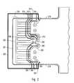
- FIG. 2illustrates a PCB 200 that is defined by the outline 218 .
- the area 224 between the contacts 220 and a front edge 221 of the PCB 200does not include any traces such as the traces 104 illustrated in FIG. 1 .
- the contact pads 220 along with other conductive paths within and/or on the PCB 200are typically plated with hard gold (or other suitable material). In this example, traces are used to form a single conductive path between the contact pads 220 and other conductive paths and a plating bar 202 .
- the tracesillustrated as traces 210 , 212 , 214 , 216 , 204 , 206 , and 208 , lead from a conductive path on the PCB 200 to a side edge of the PCB 200 .
- the tracesare on an internal layer of the PCB 200 .
- the traces 210 , 212 , 214 , 216 , 204 , 206 , and 208do not lead to the front edge 221 of the PCB 200 .
- the trace 206leads from a side edge of the PCB 200 to a via 252 .
- This portion of the trace 206is likely on an internal layer of the PCB 200 .
- a trace from the via 252 to one of the contact pads 220completes the trace.
- This portion of the trace 206 from the via 252 to the contactmay be on an external layer or on another internal layer of the PCB 200 .
- Other contact pads 220have a trace that can be followed to a side edge of the PCB 200 .
- the portion of the trace from the contact pad to a viamay be on an external layer of the PCB 200 while the remaining portion of the trace from the via to the side edge of the PCB is on an internal layer of the PCB.
- the viasare used to provide a connection from the external layer of the PCB to the internal layers of the PCB.
- the traces 210 , 212 , 214 , 216 , 204 , 206 , and 208can exist on different layers of the PCB 200 . This often occurs in order to insure that the various conductive paths are electrically isolated when the PCB 200 is routed to the outline 218 .
- the traces 210 , 212 , 214 , 216 , 204 , 206 , and 208when connected with the plating bar 202 , cause the contact pads, vias, signal paths, etc. on the PCB 200 to form a single conductive path in one embodiment. A current or voltage can then be used to plate all of the conductive paths at the same time. After the conductive paths such as the contact pads are plated, the PCB is cut or routed to a final outline (indicated by the outline 218 ). By cutting the PCB 200 to the outline 218 the connections between the traces 210 , 212 , 214 , 216 , 204 , 206 , and 208 is removed and the various conductive paths of the PCB 200 are electrically isolated.
- FIG. 3illustrates another embodiment of the present invention that also relates to plating transmission lines or high speed traces.
- the PCB 300 in this exampleincludes transmission lines 320 , 322 , 324 , and 326 . Because transmission lines may be sensitive to impedances, it is undesirable to have long stubs. For example, if a trace is formed from the transmission line 322 over to a side edge of the PCB 300 , then the trace would form a long stub and would remain attached to the transmission line 322 after the PCB was routed to a final form factor. This trace would be similar to the traces 210 , 212 , 214 , 216 , 204 , 206 , and 208 illustrated in FIG. 2 .
- a trace 370is formed from a transmission line 320 to a nearby contact 321 that is not affected by longer stubs.
- the trace 370may connect to another signal such as a ground plane and the like.
- FIG. 4is an expanded view of a particular portion 350 of FIG. 3 .
- the process for plating the high speed transmission lines 320 and 322begins by forming a trace to a nearby conductive path or signal.
- the transmission line 320is connected with the contact 321 using a trace 370 and the transmission line 322 connects with a contact 323 using a trace 372 , as shown in FIG. 3 .
- the particular contacts 323 and 321may be connected to a plating bar using another trace.
- the trace 370 A of trace 370is formed from the transmission line 320 to a via 376 either on a top layer of the PCB or on an internal layer of the PCB.
- the trace 370 Bconnects to the trace 370 A through the via 376 and the trace 370 B connects to the contact 321 .
- the trace 372 A of trace 372is formed from the transmission line 322 to a via 374 either on a top layer of the PCB or on an internal layer of the PCB.
- the trace 372 Bconnects to the trace 372 A through the via 374 and the trace 372 B connects to the contact 323 .
- the traces illustrated in FIG. 2are not shown for clarity although they are present in order to plate all conductive paths of the PCB as previously described. Using the traces 372 and 370 , the high speed transmission lines are plated during the plating process.
- a drilling processcreates small holes 356 and 358 in the traces 370 A and 372 A respectively to disconnect the traces 370 and 372 , respectively, from the high speed transmission lines.
- short stubs 352 and 354remain, but these short stubs do not adversely affect the integrity of the high-speed traces to which they are attached. By controlling the drilling process, the length of the short stubs 352 and 354 can be negligible.
- plating the transmission lines using a trace as described with reference to FIG. 2leaves a long stub from the transmission line to the edge of the PCB. This long stub may have an adverse effect on the transmission line.
- the transmission linesmay be plated using traces as described with FIG. 2 in combination with a drilling process that results in a short stub as described.
- a short stubis left.
- the length of the stubcan be controlled by drilling holes that are close to the transmission lines.
- FIG. 5illustrates a plurality of PCB boards 500 that are all connected during the fabrication of the PCBs including the plating process.
- the PCB boards 500are cut into separate PCB boards 502 , 504 , 506 , and 508 by separating the individual PCB boards along the dashed lines 510 , 512 , and 514 .
- a drilling processthen forms holes such that the high speed transmission lines are not connected to long stubs that may adversely affect the transmission ability of the transmission lines. The drilling process may occur before the individual PCB are routed.
Landscapes
- Engineering & Computer Science (AREA)
- Manufacturing & Machinery (AREA)
- Microelectronics & Electronic Packaging (AREA)
- Printing Elements For Providing Electric Connections Between Printed Circuits (AREA)
- Optical Couplings Of Light Guides (AREA)
Abstract
Description
- This application is a continuation, and claims the benefit, of U.S. patent application Ser. No. 10/762,860, entitled SYSTEMS AND METHODS FOR FABRICATING PRINTED CIRCUIT BOARDS, filed Jan. 22, 2004, which, in turn, claims the benefit of U.S. Provisional Patent Application No. 60/483,702, entitled SYSTEMS AND METHODS FOR FABRICATING PRINTED CIRCUIT BOARDS, filed Jun. 30, 2003. All of the aforementioned applications are incorporated herein by this reference.
- 1. The Field of the Invention
- The present invention generally relates to printed circuit boards (PCBs). More particularly, the present invention relates to systems and methods for fabricating printed circuit boards and more specifically to systems and methods for plating traces on PCBs.
- 2. Related Technology
- An integral component of many electrical and optical devices is a multi-layer printed circuit board (PCB). PCBs are used, for example, to route signals and provide connections to various electrical and/or optical components. During plating, which is one of the steps that occurs during the fabrication of a PCB for example, some or all of the traces, vias, pads, etc., are plated with hard gold. Plating ensures that the PCB can make a solid electrical connection and strengthens the electrical integrity of the PCB. Usually, all features of the PCB requiring plating are plated at the same time.
- The typical plating process involves shorting all the contact pads by connecting them to small traces, which extend off the front edge of the PCB. The small traces then connect to a plating bar and a voltage is applied. By connecting all of the traces to a plating bar, all of the signal paths requiring plating in the PCB form a single conductive path. By applying a voltage, the resulting current electronically plates the gold on to the contact pads. In other words, all necessary signal paths are plated with hard gold at the same time. After the plating process is complete, the traces used to plate the appropriate portions of the PCB are cut at the front edge of the PCB, thus eliminating the short between the contact pads. One of the problems with this process is that small traces that extend from the contact pads to the front edge of the PCB remain on the PCB.
- This problem is illustrated in
FIG. 1 where the traces used to plate the contact pads (and other traces, signals, vias, etc. of the PCB) remain after the PCB has been routed to a final form factor. InFIG. 1 , thecontact pads 102 provide electrical access to the signal or conductive paths of thePCB 100. As previously described during the plating process, thetraces 104 were formed and connected to a plating bar (not shown). Thus, thePCB 100 illustrates thetraces 104 that were used to plate thecontact pads 102 and other conductive paths of thePCB 100. Note thatFIG. 1 illustrates the contact pads of thePCB 100, but it is understood that the other conductive paths that are connected with the contact pads are also plated. - Unfortunately, the
traces 104 are in thearea 106 between afront edge 103 of the PCB and thecontact pads 102. The presence of thesmall traces 104 in thearea 106 of the PCB100 may violate certain standards. In particular, thetraces 104 may violate the GBIC/MSA standard. This standard requires that the contact pads within a GBIC/MSA device be set back from the PCB edge. Other small form factor pluggable standards (GBIC, SFP, XFP) may have similar requirements. - Another problem produced by the typical plating process is that it may interfere with high-speed traces, which are connected to certain contact pads. The purpose of the high-speed traces is to send high-speed data through the PCB. To achieve this purpose, high-speed traces involve careful balancing of impedances. The small traces that extend from the contact pads to the edge of the PCB disrupt this balance and reduce the ability of the high speed traces to effectively transfer data at high speeds. Cutting the small traces produces large stubs at the edge of the PCB, which do not affect performance of low speed traces but create interference among the high-speed traces and adversely affect the performance of these high-speed lines.
- Previous attempts to improve the plating process and eliminate the extension of small traces to the front edge of the PCB have been unsatisfactory. For example, etching, a technique employed to remove the
small traces 104 from thearea 106 of the PCB after the plating process, is expensive for use in low-cost transceiver modules. - Exemplary embodiments of the present invention relate to printed circuit boards and optical transceivers in which such printed circuit boards may be employed. In one example, an optical transceiver includes a housing and an optical transmitter and optical receiver disposed within the housing. A PCB is also disposed in the housing. The PCB has front and side edges, as well as circuitry in communication with the optical transmitter and the optical receiver. The PCB also includes a group of plated contact pads, each of which includes a front-most extremity that terminates short of the front edge. Finally, the PCB includes a group of traces, one of which leads from one of the side edges of the PCB to a via that is connected with the circuitry, and another of which leads from the via to one of the plated contact pads.
- These and other aspects of the present invention will become more fully apparent from the following description and appended claims.
- To further clarify the above and other advantages and features of the present invention, a more particular description of the invention will be rendered by reference to specific embodiments thereof which are illustrated in the appended drawings. It is appreciated that these drawings depict only typical embodiments of the invention and are therefore not to be considered limiting of its scope. The invention will be described and explained with additional specificity and detail through the use of the accompanying drawings in which:
FIG. 1 illustrates a top view of a PCB having traces that extend from a front edge of the PCB to the contact pads of the PCB;FIG. 2 illustrates a view of the top external layer of a PCB that is plated without leaving traces between the edge of the PCB and the contact pads;FIG. 3 illustrates a top view of a PCB where a high speed transmission line is plated;FIG. 4 is a magnified view of a portion of the PCB inFIG. 3 and illustrates plated transmission lines; andFIG. 5 illustrates a board that includes multiple PCBs that are all plated at the same time.- The present invention relates to systems and methods for fabricating printed circuit boards (PCBs) and more particularly to plating conductive paths including contact pads of PCBs. The present invention has the advantage of eliminating the small plated traces that extend to the front edge of a PCB from the contact pads and also of minimizing the stub length on high speed transmission lines on the PCB that are formed during the conventional plating process.
- To eliminate the small traces extending to the front edge of the PCB, the contact pads on the external layer are connected to traces on an internal layer(s) of the PCB. The external contact pads are connected to the internal traces through vias, small pathways running between the layers of the PCB. The vias are formed through the multi-layer PCB by a drilling operation performed before the plating process. The traces lead to the sides of the PCB instead of to the front edge of the PCB. During the plating process metal is deposited through the vias onto each layer of the PCB.
- As indicated, the traces on the internal layer(s) are routed to the sides of the PCB where are attached to an external plating bar. The external plating bar serves to short all the connections from the traces together at one central point. In this example, the PCB includes a single conductive path. Once the traces are attached to the plating bar, a current or voltage is used to deposit the gold onto the contact pads, conductive paths, vias, traces, and the like.
- Plating the high speed traces or transmission lines on a PCB can result in problems as the traces used to plate the high speed traces may form long stubs that interfere with the impedance of the high speed traces. In one embodiment, thin traces connect the high-speed traces to ground pins located on the PCB near the high-speed traces and thus create a short during the plating process between the ground pins and the high-speed traces. After completion of the plating process, a hole is drilled through the thin trace, thus removing the short. The hole leaves a very short stub that will not adversely affect performance of the high-speed trace, unlike the large stubs created when a connecting trace is routed to the side of the PCB.
- The present invention is described in terms of a PCB used, for example, in Gigabit Interface Converters (“GBIC”) devices such as GBIC optical transceivers. One of skill in the art, however, can appreciate that the present invention relates generally to PCBs and is not limited to PCBs used in specific devices. Embodiments of the present invention thus extend to PCBs that can be implemented, for example, in SFP, XFP devices, and the like.
- As illustrated in
FIG. 1 , current plating technologies leavetraces 104 that are undesirable in some instances. Specifically, the plated traces104 may violate the specifications of some standards such as the GBIC/MSA standard.FIG. 2 illustrates a PCB fabricated in accordance with one embodiment of the present invention that eliminates thetraces 104 as illustrated inFIG. 1 . FIG. 2 illustrates a PCB200 that is defined by theoutline 218. As illustrated, thearea 224 between thecontacts 220 and afront edge 221 of the PCB200 does not include any traces such as thetraces 104 illustrated inFIG. 1 . Thecontact pads 220 along with other conductive paths within and/or on the PCB200 are typically plated with hard gold (or other suitable material). In this example, traces are used to form a single conductive path between thecontact pads 220 and other conductive paths and aplating bar 202. The traces, illustrated astraces - The
traces front edge 221 of the PCB200. For example, thetrace 206 leads from a side edge of the PCB200 to a via252. This portion of thetrace 206 is likely on an internal layer of the PCB200. A trace from the via252 to one of thecontact pads 220 completes the trace. This portion of thetrace 206 from the via252 to the contact, however, may be on an external layer or on another internal layer of the PCB200.Other contact pads 220 have a trace that can be followed to a side edge of the PCB200. As previously stated, the portion of the trace from the contact pad to a via may be on an external layer of the PCB200 while the remaining portion of the trace from the via to the side edge of the PCB is on an internal layer of the PCB. The vias are used to provide a connection from the external layer of the PCB to the internal layers of the PCB. In one embodiment, thetraces outline 218. - The
traces plating bar 202, cause the contact pads, vias, signal paths, etc. on the PCB200 to form a single conductive path in one embodiment. A current or voltage can then be used to plate all of the conductive paths at the same time. After the conductive paths such as the contact pads are plated, the PCB is cut or routed to a final outline (indicated by the outline218). By cutting the PCB200 to theoutline 218 the connections between thetraces FIG. 3 illustrates another embodiment of the present invention that also relates to plating transmission lines or high speed traces. The PCB300 in this example, includestransmission lines transmission line 322 over to a side edge of the PCB300, then the trace would form a long stub and would remain attached to thetransmission line 322 after the PCB was routed to a final form factor. This trace would be similar to thetraces FIG. 2 .- As illustrated in
FIG. 3 , atrace 370 is formed from atransmission line 320 to anearby contact 321 that is not affected by longer stubs. In one embodiment, thetrace 370 may connect to another signal such as a ground plane and the like. This is more clearly illustrated inFIG. 4 , which is an expanded view of aparticular portion 350 ofFIG. 3 . The process for plating the highspeed transmission lines transmission line 320 is connected with thecontact 321 using atrace 370 and thetransmission line 322 connects with acontact 323 using atrace 372, as shown inFIG. 3 . As illustrated and described inFIG. 2 , theparticular contacts - In this example, the
trace 370A oftrace 370 is formed from thetransmission line 320 to a via376 either on a top layer of the PCB or on an internal layer of the PCB. Thetrace 370B connects to thetrace 370A through the via376 and thetrace 370B connects to thecontact 321. In a similar fashion, thetrace 372A oftrace 372 is formed from thetransmission line 322 to a via374 either on a top layer of the PCB or on an internal layer of the PCB. Thetrace 372B connects to thetrace 372A through the via374 and thetrace 372B connects to thecontact 323. For this example, the traces illustrated inFIG. 2 are not shown for clarity although they are present in order to plate all conductive paths of the PCB as previously described. Using thetraces - After the plating process has been completed and the transmission lines are plated, a drilling process creates
small holes traces traces short stubs short stubs - In contrast, plating the transmission lines using a trace as described with reference to
FIG. 2 leaves a long stub from the transmission line to the edge of the PCB. This long stub may have an adverse effect on the transmission line. - In another embodiment, the transmission lines may be plated using traces as described with
FIG. 2 in combination with a drilling process that results in a short stub as described. In each embodiment, a short stub is left. The length of the stub, however can be controlled by drilling holes that are close to the transmission lines. - In another embodiment, more that one PCB can be plated at the same time.
FIG. 5 , for example, illustrates a plurality ofPCB boards 500 that are all connected during the fabrication of the PCBs including the plating process. At a later stage of PCB fabrication, thePCB boards 500 are cut intoseparate PCB boards lines - The present invention may be embodied in other specific forms without departing from its spirit or essential characteristics. The described embodiments are to be considered in all respects only as illustrative and not restrictive. The scope of the invention is, therefore, indicated by the appended claims rather than by the foregoing description. All changes which come within the meaning and range of equivalency of the claims are to be embraced within their scope.
Claims (21)
Priority Applications (1)
| Application Number | Priority Date | Filing Date | Title |
|---|---|---|---|
| US11/298,139US7663890B2 (en) | 2003-06-30 | 2005-12-09 | Printed circuit boards for use in optical transceivers |
Applications Claiming Priority (3)
| Application Number | Priority Date | Filing Date | Title |
|---|---|---|---|
| US48370203P | 2003-06-30 | 2003-06-30 | |
| US10/762,860US7020960B2 (en) | 2003-06-30 | 2004-01-22 | Systems and methods for fabricating printed circuit boards |
| US11/298,139US7663890B2 (en) | 2003-06-30 | 2005-12-09 | Printed circuit boards for use in optical transceivers |
Related Parent Applications (1)
| Application Number | Title | Priority Date | Filing Date |
|---|---|---|---|
| US10/762,860ContinuationUS7020960B2 (en) | 2003-06-30 | 2004-01-22 | Systems and methods for fabricating printed circuit boards |
Publications (2)
| Publication Number | Publication Date |
|---|---|
| US20060118331A1true US20060118331A1 (en) | 2006-06-08 |
| US7663890B2 US7663890B2 (en) | 2010-02-16 |
Family
ID=33544691
Family Applications (2)
| Application Number | Title | Priority Date | Filing Date |
|---|---|---|---|
| US10/762,860Expired - Fee RelatedUS7020960B2 (en) | 2003-06-30 | 2004-01-22 | Systems and methods for fabricating printed circuit boards |
| US11/298,139Expired - LifetimeUS7663890B2 (en) | 2003-06-30 | 2005-12-09 | Printed circuit boards for use in optical transceivers |
Family Applications Before (1)
| Application Number | Title | Priority Date | Filing Date |
|---|---|---|---|
| US10/762,860Expired - Fee RelatedUS7020960B2 (en) | 2003-06-30 | 2004-01-22 | Systems and methods for fabricating printed circuit boards |
Country Status (1)
| Country | Link |
|---|---|
| US (2) | US7020960B2 (en) |
Cited By (6)
| Publication number | Priority date | Publication date | Assignee | Title |
|---|---|---|---|---|
| US20090142939A1 (en)* | 2007-12-03 | 2009-06-04 | Hon Hai Precision Ind. Co., Ltd. | Adapter for card connector |
| US20090229859A1 (en)* | 2008-03-11 | 2009-09-17 | Alcatel Lucent | 10G XFP compliant PCB |
| US20110132648A1 (en)* | 2009-12-08 | 2011-06-09 | International Business Machines Corporation | Channel performance of electrical lines |
| WO2013003472A3 (en)* | 2011-06-29 | 2013-02-28 | Finisar Corporation | Multichannel rf feedthroughs |
| US20130121636A1 (en)* | 2011-11-14 | 2013-05-16 | Aci Communications, Inc. | Optical node configuration apparatus |
| US10512155B2 (en)* | 2016-01-27 | 2019-12-17 | Kyocera Corporation | Wiring board, optical semiconductor element package, and optical semiconductor device |
Families Citing this family (13)
| Publication number | Priority date | Publication date | Assignee | Title |
|---|---|---|---|---|
| TWI290015B (en)* | 2005-07-01 | 2007-11-11 | Via Tech Inc | Circuit board with plating bar |
| JP4669338B2 (en)* | 2005-07-22 | 2011-04-13 | 富士通コンポーネント株式会社 | Printed wiring board and manufacturing method thereof |
| US7427719B2 (en)* | 2006-03-21 | 2008-09-23 | Intel Corporation | Shifted segment layout for differential signal traces to mitigate bundle weave effect |
| US8168891B1 (en)* | 2007-10-26 | 2012-05-01 | Force10 Networks, Inc. | Differential trace profile for printed circuit boards |
| US8764464B2 (en)* | 2008-02-29 | 2014-07-01 | Fci Americas Technology Llc | Cross talk reduction for high speed electrical connectors |
| US9277649B2 (en)* | 2009-02-26 | 2016-03-01 | Fci Americas Technology Llc | Cross talk reduction for high-speed electrical connectors |
| KR101356472B1 (en)* | 2011-07-01 | 2014-02-03 | 샘텍, 인코포레이티드 | Transceiver and interface for ic package |
| CN107548530A (en) | 2016-04-29 | 2018-01-05 | 慧与发展有限责任合伙企业 | Press-fit pin converter |
| US10288825B2 (en)* | 2016-12-23 | 2019-05-14 | Hisense Broadband Multimedia Technologies Co., Ltd. | Optical module |
| CN109980400B (en)* | 2017-12-28 | 2021-07-23 | 泰科电子(上海)有限公司 | Connector |
| CN109982504B (en)* | 2017-12-28 | 2021-06-25 | 泰科电子(上海)有限公司 | Circuit boards and boards |
| CN112004323B (en)* | 2020-08-20 | 2021-08-03 | 之江实验室 | A design method of equal-length wiring between MCU and SDRAM in BGA package |
| US11924964B2 (en)* | 2022-04-07 | 2024-03-05 | Western Digital Technologies, Inc. | Printed circuit board for galvanic effect reduction |
Citations (13)
| Publication number | Priority date | Publication date | Assignee | Title |
|---|---|---|---|---|
| US3128332A (en)* | 1960-03-30 | 1964-04-07 | Hughes Aircraft Co | Electrical interconnection grid and method of making same |
| US3142112A (en)* | 1960-03-30 | 1964-07-28 | Hughes Aircraft Co | Method of making an electrical interconnection grid |
| US3718936A (en)* | 1971-06-16 | 1973-02-27 | American Express Invest | Electrostatic matrix head construction |
| US4560962A (en)* | 1983-08-30 | 1985-12-24 | Burroughs Corporation | Multilayered printed circuit board with controlled 100 ohm impedance |
| US4764806A (en)* | 1986-10-27 | 1988-08-16 | Tds Patent Management, Inc. | Aplanatic image combiner for use in projection television systems with reduced spherical and coma aberration |
| US4859806A (en)* | 1988-05-17 | 1989-08-22 | Microelectronics And Computer Technology Corporation | Discretionary interconnect |
| US4890157A (en)* | 1986-01-31 | 1989-12-26 | Texas Instruments Incorporated | Integrated circuit product having a polyimide film interconnection structure |
| US6250820B1 (en)* | 1997-02-28 | 2001-06-26 | Infineon Technologies Ag | Electrooptical coupling component |
| US6479765B2 (en)* | 2000-06-26 | 2002-11-12 | Robinson Nugent, Inc. | Vialess printed circuit board |
| US6486549B1 (en)* | 2001-11-10 | 2002-11-26 | Bridge Semiconductor Corporation | Semiconductor module with encapsulant base |
| US6788546B1 (en)* | 1999-03-19 | 2004-09-07 | Elmicron Ag | Multi-chip module |
| US6794741B1 (en)* | 2001-07-27 | 2004-09-21 | Bridge Semiconductor Corporation | Three-dimensional stacked semiconductor package with pillars in pillar cavities |
| US6812803B2 (en)* | 2002-02-05 | 2004-11-02 | Force10 Networks, Inc. | Passive transmission line equalization using circuit-board thru-holes |
- 2004
- 2004-01-22USUS10/762,860patent/US7020960B2/ennot_activeExpired - Fee Related
- 2005
- 2005-12-09USUS11/298,139patent/US7663890B2/ennot_activeExpired - Lifetime
Patent Citations (13)
| Publication number | Priority date | Publication date | Assignee | Title |
|---|---|---|---|---|
| US3128332A (en)* | 1960-03-30 | 1964-04-07 | Hughes Aircraft Co | Electrical interconnection grid and method of making same |
| US3142112A (en)* | 1960-03-30 | 1964-07-28 | Hughes Aircraft Co | Method of making an electrical interconnection grid |
| US3718936A (en)* | 1971-06-16 | 1973-02-27 | American Express Invest | Electrostatic matrix head construction |
| US4560962A (en)* | 1983-08-30 | 1985-12-24 | Burroughs Corporation | Multilayered printed circuit board with controlled 100 ohm impedance |
| US4890157A (en)* | 1986-01-31 | 1989-12-26 | Texas Instruments Incorporated | Integrated circuit product having a polyimide film interconnection structure |
| US4764806A (en)* | 1986-10-27 | 1988-08-16 | Tds Patent Management, Inc. | Aplanatic image combiner for use in projection television systems with reduced spherical and coma aberration |
| US4859806A (en)* | 1988-05-17 | 1989-08-22 | Microelectronics And Computer Technology Corporation | Discretionary interconnect |
| US6250820B1 (en)* | 1997-02-28 | 2001-06-26 | Infineon Technologies Ag | Electrooptical coupling component |
| US6788546B1 (en)* | 1999-03-19 | 2004-09-07 | Elmicron Ag | Multi-chip module |
| US6479765B2 (en)* | 2000-06-26 | 2002-11-12 | Robinson Nugent, Inc. | Vialess printed circuit board |
| US6794741B1 (en)* | 2001-07-27 | 2004-09-21 | Bridge Semiconductor Corporation | Three-dimensional stacked semiconductor package with pillars in pillar cavities |
| US6486549B1 (en)* | 2001-11-10 | 2002-11-26 | Bridge Semiconductor Corporation | Semiconductor module with encapsulant base |
| US6812803B2 (en)* | 2002-02-05 | 2004-11-02 | Force10 Networks, Inc. | Passive transmission line equalization using circuit-board thru-holes |
Cited By (12)
| Publication number | Priority date | Publication date | Assignee | Title |
|---|---|---|---|---|
| US20090142939A1 (en)* | 2007-12-03 | 2009-06-04 | Hon Hai Precision Ind. Co., Ltd. | Adapter for card connector |
| US20090229859A1 (en)* | 2008-03-11 | 2009-09-17 | Alcatel Lucent | 10G XFP compliant PCB |
| US7746657B2 (en)* | 2008-03-11 | 2010-06-29 | Alcatel Lucent | 10G XFP compliant PCB |
| US20110132648A1 (en)* | 2009-12-08 | 2011-06-09 | International Business Machines Corporation | Channel performance of electrical lines |
| US8325459B2 (en)* | 2009-12-08 | 2012-12-04 | International Business Machines Corporation | Channel performance of electrical lines |
| WO2013003472A3 (en)* | 2011-06-29 | 2013-02-28 | Finisar Corporation | Multichannel rf feedthroughs |
| CN103703396A (en)* | 2011-06-29 | 2014-04-02 | 菲尼萨公司 | Multichannel rf feedthroughs |
| US9538637B2 (en) | 2011-06-29 | 2017-01-03 | Finisar Corporation | Multichannel RF feedthroughs |
| US20130121636A1 (en)* | 2011-11-14 | 2013-05-16 | Aci Communications, Inc. | Optical node configuration apparatus |
| US20130202296A1 (en)* | 2011-11-14 | 2013-08-08 | Aci Communications, Inc. | Optical node configuration apparatus |
| US9231703B2 (en)* | 2011-11-14 | 2016-01-05 | Aci Communications, Inc. | Optical node configuration apparatus |
| US10512155B2 (en)* | 2016-01-27 | 2019-12-17 | Kyocera Corporation | Wiring board, optical semiconductor element package, and optical semiconductor device |
Also Published As
| Publication number | Publication date |
|---|---|
| US7020960B2 (en) | 2006-04-04 |
| US7663890B2 (en) | 2010-02-16 |
| US20040261263A1 (en) | 2004-12-30 |
Similar Documents
| Publication | Publication Date | Title |
|---|---|---|
| US7663890B2 (en) | Printed circuit boards for use in optical transceivers | |
| US10194524B1 (en) | Anti-pad for signal and power vias in printed circuit board | |
| US9560774B2 (en) | Method of fabricating a circuit board | |
| US7200010B2 (en) | Impedance qualization module | |
| US7013452B2 (en) | Method and apparatus for intra-layer transitions and connector launch in multilayer circuit boards | |
| US11490504B2 (en) | High-speed trace breakout methods and systems | |
| CN108075261A (en) | The connection method of the connection structure of substrate and connector, substrate and substrate and connector | |
| US10455690B1 (en) | Grid array pattern for crosstalk reduction | |
| US20240164018A1 (en) | Non-uniform surface mount pads | |
| US8525611B2 (en) | Enhanced electromagnetic coupling between a transmission line pair with reduced electromagnetic coupling to ground | |
| US20140167886A1 (en) | Plating Stub Resonance Shift with Filter Stub Design Methodology | |
| US20070132527A1 (en) | Suppression method and structure for reducing a via stub effect of a substrate | |
| US20080087460A1 (en) | Apparatus and method for a printed circuit board that reduces capacitance loading of through-holes | |
| JP5561428B2 (en) | Transmission system and backplane system construction method | |
| CN110637399B (en) | Optical module and its manufacturing method | |
| US5880657A (en) | Printed wiring board modified gull wing signal lead connection | |
| EP0204004A1 (en) | Wiring structure of a terminal circuit | |
| JP2013065657A (en) | Printed wiring board, and method for wiring printed wiring board | |
| US11477890B2 (en) | Plated pads and leads for surface mount technology connections | |
| CN103025082B (en) | A method of manufacturing a printed circuit board and a printed circuit board structure | |
| CN223093962U (en) | PCB structure for optimizing return loss of through hole connector | |
| US11617265B1 (en) | Electronic device | |
| CN114501850B (en) | Via hole design method, via hole, PCB board, PCB design and production method | |
| JP2009123958A (en) | Method for manufacturing printed circuit board | |
| CN221448651U (en) | PCB structure of high-speed connector bonding pad and circuit board mounted with high-speed connector |
Legal Events
| Date | Code | Title | Description |
|---|---|---|---|
| STCF | Information on status: patent grant | Free format text:PATENTED CASE | |
| FPAY | Fee payment | Year of fee payment:4 | |
| FPAY | Fee payment | Year of fee payment:8 | |
| AS | Assignment | Owner name:FINISAR CORPORATION, CALIFORNIA Free format text:ASSIGNMENT OF ASSIGNORS INTEREST;ASSIGNORS:NELSON, STEPHEN;WHITE, DONALD;REEL/FRAME:049258/0990 Effective date:20031215 | |
| AS | Assignment | Owner name:BANK OF AMERICA, N.A., AS ADMINISTRATIVE AGENT, NO Free format text:NOTICE OF GRANT OF SECURITY INTEREST IN PATENTS;ASSIGNORS:II-VI INCORPORATED;MARLOW INDUSTRIES, INC.;EPIWORKS, INC.;AND OTHERS;REEL/FRAME:050484/0204 Effective date:20190924 Owner name:BANK OF AMERICA, N.A., AS ADMINISTRATIVE AGENT, NORTH CAROLINA Free format text:NOTICE OF GRANT OF SECURITY INTEREST IN PATENTS;ASSIGNORS:II-VI INCORPORATED;MARLOW INDUSTRIES, INC.;EPIWORKS, INC.;AND OTHERS;REEL/FRAME:050484/0204 Effective date:20190924 | |
| AS | Assignment | Owner name:II-VI DELAWARE, INC., DELAWARE Free format text:ASSIGNMENT OF ASSIGNORS INTEREST;ASSIGNOR:FINISAR CORPORATION;REEL/FRAME:052286/0001 Effective date:20190924 | |
| MAFP | Maintenance fee payment | Free format text:PAYMENT OF MAINTENANCE FEE, 12TH YEAR, LARGE ENTITY (ORIGINAL EVENT CODE: M1553); ENTITY STATUS OF PATENT OWNER: LARGE ENTITY Year of fee payment:12 | |
| AS | Assignment | Owner name:JPMORGAN CHASE BANK, N.A., AS COLLATERAL AGENT, NEW YORK Free format text:SECURITY INTEREST;ASSIGNORS:II-VI INCORPORATED;II-VI DELAWARE, INC.;M CUBED TECHNOLOGIES, INC.;AND OTHERS;REEL/FRAME:060562/0254 Effective date:20220701 | |
| AS | Assignment | Owner name:PHOTOP TECHNOLOGIES, INC., CALIFORNIA Free format text:PATENT RELEASE AND REASSIGNMENT;ASSIGNOR:BANK OF AMERICA, N.A., AS ADMINISTRATIVE AGENT;REEL/FRAME:060574/0001 Effective date:20220701 Owner name:II-VI OPTOELECTRONIC DEVICES, INC., NEW JERSEY Free format text:PATENT RELEASE AND REASSIGNMENT;ASSIGNOR:BANK OF AMERICA, N.A., AS ADMINISTRATIVE AGENT;REEL/FRAME:060574/0001 Effective date:20220701 Owner name:II-VI DELAWARE, INC., PENNSYLVANIA Free format text:PATENT RELEASE AND REASSIGNMENT;ASSIGNOR:BANK OF AMERICA, N.A., AS ADMINISTRATIVE AGENT;REEL/FRAME:060574/0001 Effective date:20220701 Owner name:II-VI PHOTONICS (US), INC., MASSACHUSETTS Free format text:PATENT RELEASE AND REASSIGNMENT;ASSIGNOR:BANK OF AMERICA, N.A., AS ADMINISTRATIVE AGENT;REEL/FRAME:060574/0001 Effective date:20220701 Owner name:M CUBED TECHNOLOGIES, INC., CONNECTICUT Free format text:PATENT RELEASE AND REASSIGNMENT;ASSIGNOR:BANK OF AMERICA, N.A., AS ADMINISTRATIVE AGENT;REEL/FRAME:060574/0001 Effective date:20220701 Owner name:II-VI OPTICAL SYSTEMS, INC., CALIFORNIA Free format text:PATENT RELEASE AND REASSIGNMENT;ASSIGNOR:BANK OF AMERICA, N.A., AS ADMINISTRATIVE AGENT;REEL/FRAME:060574/0001 Effective date:20220701 Owner name:FINISAR CORPORATION, CALIFORNIA Free format text:PATENT RELEASE AND REASSIGNMENT;ASSIGNOR:BANK OF AMERICA, N.A., AS ADMINISTRATIVE AGENT;REEL/FRAME:060574/0001 Effective date:20220701 Owner name:OPTIUM CORPORATION, CALIFORNIA Free format text:PATENT RELEASE AND REASSIGNMENT;ASSIGNOR:BANK OF AMERICA, N.A., AS ADMINISTRATIVE AGENT;REEL/FRAME:060574/0001 Effective date:20220701 Owner name:COADNA PHOTONICS, INC., PENNSYLVANIA Free format text:PATENT RELEASE AND REASSIGNMENT;ASSIGNOR:BANK OF AMERICA, N.A., AS ADMINISTRATIVE AGENT;REEL/FRAME:060574/0001 Effective date:20220701 Owner name:KAILIGHT PHOTONICS, INC., CALIFORNIA Free format text:PATENT RELEASE AND REASSIGNMENT;ASSIGNOR:BANK OF AMERICA, N.A., AS ADMINISTRATIVE AGENT;REEL/FRAME:060574/0001 Effective date:20220701 Owner name:LIGHTSMYTH TECHNOLOGIES, INC., OREGON Free format text:PATENT RELEASE AND REASSIGNMENT;ASSIGNOR:BANK OF AMERICA, N.A., AS ADMINISTRATIVE AGENT;REEL/FRAME:060574/0001 Effective date:20220701 Owner name:EPIWORKS, INC., ILLINOIS Free format text:PATENT RELEASE AND REASSIGNMENT;ASSIGNOR:BANK OF AMERICA, N.A., AS ADMINISTRATIVE AGENT;REEL/FRAME:060574/0001 Effective date:20220701 Owner name:MARLOW INDUSTRIES, INC., TEXAS Free format text:PATENT RELEASE AND REASSIGNMENT;ASSIGNOR:BANK OF AMERICA, N.A., AS ADMINISTRATIVE AGENT;REEL/FRAME:060574/0001 Effective date:20220701 Owner name:II-VI INCORPORATED, PENNSYLVANIA Free format text:PATENT RELEASE AND REASSIGNMENT;ASSIGNOR:BANK OF AMERICA, N.A., AS ADMINISTRATIVE AGENT;REEL/FRAME:060574/0001 Effective date:20220701 |