US20060115978A1 - Charge-trapping memory cell and method for production - Google Patents
Charge-trapping memory cell and method for productionDownload PDFInfo
- Publication number
- US20060115978A1 US20060115978A1US11/000,350US35004AUS2006115978A1US 20060115978 A1US20060115978 A1US 20060115978A1US 35004 AUS35004 AUS 35004AUS 2006115978 A1US2006115978 A1US 2006115978A1
- Authority
- US
- United States
- Prior art keywords
- fins
- layer
- charge
- select transistors
- wordlines
- Prior art date
- Legal status (The legal status is an assumption and is not a legal conclusion. Google has not performed a legal analysis and makes no representation as to the accuracy of the status listed.)
- Granted
Links
Images


Classifications
- H—ELECTRICITY
- H01—ELECTRIC ELEMENTS
- H01L—SEMICONDUCTOR DEVICES NOT COVERED BY CLASS H10
- H01L21/00—Processes or apparatus adapted for the manufacture or treatment of semiconductor or solid state devices or of parts thereof
- H01L21/70—Manufacture or treatment of devices consisting of a plurality of solid state components formed in or on a common substrate or of parts thereof; Manufacture of integrated circuit devices or of parts thereof
- H01L21/71—Manufacture of specific parts of devices defined in group H01L21/70
- H01L21/768—Applying interconnections to be used for carrying current between separate components within a device comprising conductors and dielectrics
- H01L21/76838—Applying interconnections to be used for carrying current between separate components within a device comprising conductors and dielectrics characterised by the formation and the after-treatment of the conductors
- H01L21/76895—Local interconnects; Local pads, as exemplified by patent document EP0896365
- H—ELECTRICITY
- H01—ELECTRIC ELEMENTS
- H01L—SEMICONDUCTOR DEVICES NOT COVERED BY CLASS H10
- H01L21/00—Processes or apparatus adapted for the manufacture or treatment of semiconductor or solid state devices or of parts thereof
- H01L21/70—Manufacture or treatment of devices consisting of a plurality of solid state components formed in or on a common substrate or of parts thereof; Manufacture of integrated circuit devices or of parts thereof
- H01L21/71—Manufacture of specific parts of devices defined in group H01L21/70
- H01L21/768—Applying interconnections to be used for carrying current between separate components within a device comprising conductors and dielectrics
- H01L21/76897—Formation of self-aligned vias or contact plugs, i.e. involving a lithographically uncritical step
- H—ELECTRICITY
- H10—SEMICONDUCTOR DEVICES; ELECTRIC SOLID-STATE DEVICES NOT OTHERWISE PROVIDED FOR
- H10B—ELECTRONIC MEMORY DEVICES
- H10B43/00—EEPROM devices comprising charge-trapping gate insulators
- H10B43/30—EEPROM devices comprising charge-trapping gate insulators characterised by the memory core region
- H—ELECTRICITY
- H10—SEMICONDUCTOR DEVICES; ELECTRIC SOLID-STATE DEVICES NOT OTHERWISE PROVIDED FOR
- H10D—INORGANIC ELECTRIC SEMICONDUCTOR DEVICES
- H10D30/00—Field-effect transistors [FET]
- H10D30/01—Manufacture or treatment
- H10D30/021—Manufacture or treatment of FETs having insulated gates [IGFET]
- H10D30/0413—Manufacture or treatment of FETs having insulated gates [IGFET] of FETs having charge-trapping gate insulators, e.g. MNOS transistors
- H—ELECTRICITY
- H10—SEMICONDUCTOR DEVICES; ELECTRIC SOLID-STATE DEVICES NOT OTHERWISE PROVIDED FOR
- H10D—INORGANIC ELECTRIC SEMICONDUCTOR DEVICES
- H10D30/00—Field-effect transistors [FET]
- H10D30/60—Insulated-gate field-effect transistors [IGFET]
- H10D30/69—IGFETs having charge trapping gate insulators, e.g. MNOS transistors
- H—ELECTRICITY
- H10—SEMICONDUCTOR DEVICES; ELECTRIC SOLID-STATE DEVICES NOT OTHERWISE PROVIDED FOR
- H10D—INORGANIC ELECTRIC SEMICONDUCTOR DEVICES
- H10D64/00—Electrodes of devices having potential barriers
- H10D64/01—Manufacture or treatment
- H10D64/031—Manufacture or treatment of data-storage electrodes
- H10D64/037—Manufacture or treatment of data-storage electrodes comprising charge-trapping insulators
- H—ELECTRICITY
- H10—SEMICONDUCTOR DEVICES; ELECTRIC SOLID-STATE DEVICES NOT OTHERWISE PROVIDED FOR
- H10D—INORGANIC ELECTRIC SEMICONDUCTOR DEVICES
- H10D30/00—Field-effect transistors [FET]
- H10D30/60—Insulated-gate field-effect transistors [IGFET]
- H10D30/62—Fin field-effect transistors [FinFET]
- H10D30/6211—Fin field-effect transistors [FinFET] having fin-shaped semiconductor bodies integral with the bulk semiconductor substrates
Definitions
- the present inventionconcerns nonvolatile charge-trapping memory devices with increased cell density and preferred production methods of such devices.
- Nonvolatile memory cellsthat are electrically programmable and erasable can be realized as charge-trapping memory cells, which comprise a memory layer sequence of dielectric materials with a memory layer between confinement layers of dielectric material having a larger energy band gap than the memory layer.
- the memory layer sequenceis arranged between a channel region within a semiconductor body and a gate electrode provided to control the channel by means of an applied electric voltage. Charge carriers moving from source to a drain through the channel region are accelerated and gain enough energy to be able to penetrate the lower confinement layer and to be trapped within the memory layer. Alternatively, the application of a high gate voltage enables charge carriers to tunnel through the lower confinement layer and to be trapped in the memory layer. The trapped charge carriers change the threshold voltage of the cell transistor structure. Different programming states can be read by applying the appropriate reading voltages. Examples of charge-trapping memory cells are the SONOS memory cells, in which each confinement layer is an oxide and the memory layer is a nitride of the semiconductor material, usually silicon.
- Typical applications of memory productsrequire a steady miniaturization of the memory cells.
- a reduction of the area that is required by an individual memory cellcan be obtained by shrinking the cell structure or by an increase of the number of bits that can be stored within one memory cell transistor structure.
- the nitrideis removed, and the remaining spacer is used as a mask to structure the silicon dioxide layer.
- the silicon dioxide structureis then used to etch the pattern into the silicon layer.
- This process sequenceis applied to fabricate SONOS memory devices on SOI substrates.
- a narrow silicon channel with 30 nm widthwas defined using the sidewall patterning technique.
- a memory layer sequence of oxide, nitride, and oxidewas applied, on which a 100 nm thick polysilicon layer was deposited as gate material.
- the gate electrodewas also patterned by means of the sidewalls patterning technique.
- the present inventionprovides a nonvolatile memory device with increased cell density comprising charge-trapping memory cells.
- the inventionprovides means to integrate two memory transistors within the minimal lithography dimension.
- this inventionprovides a special production method for the inventive device structures.
- the charge-trapping memory cellcomprises a semiconductor substrate with a main surface carrying a plurality of parallel fins provided as bitlines and arranged at a distance of down to about 40 nm from one another, the fins having a lateral dimension with respect to the main surface of less than about 30 nm and being subdivided into a plurality of disjointed pairs of adjacent first and second fins.
- a memory layer sequenceis provided for charge-trapping and arranged on surfaces of the fins.
- a plurality of parallel wordlinesare arranged at a distance from one another across the fins, and source/drain regions are located in the fins between the wordlines and at the ends of the fins.
- a first plurality of select transistorsis located in the first fins between the plurality of wordlines and the contact areas, and a second plurality of select transistors is located in the second fins between the plurality of wordlines and the contact areas. Select lines are provided that connect the first plurality of select transistors, and further select lines are provided that connect the second plurality of select transistors.
- Preferred embodimentscomprise first and second pluralities of select transistors at both ends of the fins, at least some of the select transistors being normally-on transistors. It is advantageous that the fins can be formed in bulk substrate material.
- the contact areasare preferably located in self-aligned fashion between the first and second fin of the respective pair of fins and laterally limited by the fins.
- the method for production of a charge-trapping memory cellcomprises the following steps: a hard mask layer and a sacrificial layer are applied onto a main surface of a semiconductor substrate; a resist mask that covers parallel strips on the sacrificial layer is formed; the sacrificial layer is etched by means of the resist mask, leaving sacrificial strips, after which the resist mask is removed; a layer of a spacer material is conformally deposited and etched back to form sidewall spacers at lateral sides of the sacrificial strips; a further resist mask is applied to cover striplike areas of the main surface running transversely across the sacrificial strips; the sacrificial strips are removed except for parts that are covered by the further resist mask, which is then removed; the hard mask layer is etched using the spacers and remaining parts of the sacrificial strips as a mask; the substrate is then etched by means of the hard mask layer as a mask to form parallel fins; a dielectric material is deposited in spaces
- FIG. 1shows a diagrammatic plan view on a memory cell array according to the invention
- FIG. 2shows a cross-section through an intermediate product of an especially preferred production method
- FIG. 3shows a plan view of the structure of the resist mask used in the corresponding production step
- FIG. 4shows the cross-section according to FIG. 2 after the application of a layer of spacer material
- FIG. 5shows the cross-section according to FIG. 4 after the formation of spacers
- FIG. 6shows the plan view according to FIG. 1 after the formation of a further resist mask
- FIG. 7shows a diagrammatic plan view of the structure of the fins and contact areas
- FIG. 8shows the plan view according to FIG. 7 after the application of a further mask having openings in the areas of the select transistors.
- FIG. 9shows the cross-section according to FIG. 5 after the production of the wordlines.
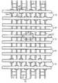
- FIG. 1shows a plan view onto the arrangement of wordlines and bitlines and the locations of the memory cells.
- the memory cellsare situated in fins 10 , which are arranged in parallel at a distance from one another. In the preferred embodiment, the distance is down to about 40 nm so that two cell transistors occupy the area of only 4F 2 .
- the finsare provided as bitlines and each comprise select transistors so that every memory cell can be addressed individually.
- FIG. 1shows the select lines 13 leading to the select transistors 14 , 14 ′ that are arranged at the ends of the fins 10 .
- the contact areas 11 of the fins 10are preferably arranged self-aligned to the fins 10 .
- the extremely reduced dimension of the finsis achieved by means of the spacer technology according to the publications mentioned above.
- charge-trapping memory cellswill be further explained by the description of an especially adapted production method.
- This processis integrated in the standard CMOS process, including the preparation of the substrate with n-doped and p-doped wells. Shallow trench isolations are formed where necessary.
- FIG. 2shows a substrate 1 , which is a semiconductor bulk, having a main surface on which a hard mask layer 2 , preferably of silicon nitride, and a sacrificial layer 3 , for example amorphous silicon or polysilicon having very small grain diameters, are applied.
- a resist mask 4is formed on the sacrificial layer 3 and may be trimmed into the shape shown by dashed lines.
- FIG. 3shows the structure of the resist mask 4 in a plan view.
- the dashed linesshow the limits of the mask openings after an optional trimming of the resist to obtain smaller resist strips.
- the (trimmed) resist mask. 4is used to structure the sacrificial layer 3 .
- the remaining parts of the sacrificial layer 3are strips having the lateral dimensions indicated by the vertical dashed lines in FIG. 2 .
- FIG. 4shows a cross-section according to FIG. 2 after the application of a layer 50 of spacer material.
- This layeris conformally deposited on the whole surface so that its thickness is essentially uniform.
- the dotted lines in FIG. 4show the limits of the intended sidewall spacers.
- These spacersare produced in the way which is known per se by an anisotropic etching in the vertical direction. This anisotropic etching reduces the thickness of the layer 50 uniformly in the direction perpendicular to the main surface of the substrate 1 .
- the sections of the layer 50 which are adjacent to the strips of the sacrificial layer 3have comparatively larger vertical dimensions so that after the etching, which is performed down to the surface of the hard mask layer 2 , only sidewall spacers of the indicated shape remain.
- FIG. 5shows the cross-section according to FIG. 4 after the anisotropic etching of the spacers 5 .
- the spacers 5have a width, which is much smaller than a corresponding dimension, which is obtained by standard lithography.
- the spacers 5are then used as a mask to etch trenches into the hard mask layer 2 and the substrate 1 , which are indicated with dashed lines in the cross-section of FIG. 5 .
- the remaining semiconductor material between the trenchesforms the fins in the substrate 1 .
- the spacer materialis preferably silicon oxide. If the hard mask layer is nitride, the hard mask layer and the semiconductor substrate can be etched selectively to the oxide of the spacers 5 .
- FIG. 6shows a diagrammatical plan view onto an intermediate product, before the remaining parts of the sacrificial layer 3 are removed.
- a further resist mask 6is applied to the surface, which covers the regions provided for the contact areas of the fins. Therefore, when the sacrificial layer 3 is removed between the spacers 5 , it is left in the areas that are provided for the contact areas.
- the surface of the substrate 1is structured into fins running parallel to one another and being arranged at a distance from one another, disjointed pairs of two neighboring fins being connected by the semiconductor material of the contact areas. The trenches between the fins are thus limited to the regions outside the contact areas.
- the semiconductor material of the substrate 1has been doped to a suitable depth to form separate electrically conductive bitlines along the fins. Therefore, each pair of fins can be addressed via the contact area at the end of the two fins belonging to the respective pair. In order to enable an address of each bitline separately, select transistors are provided that switch each bitline individually.
- FIG. 7shows the diagrammatic plan view according to FIG. 6 after the etching of the trenches to form the fins 10 and the removal of the further resist mask 6 to lay bare the contact areas 11 that limit the trenches in the longitudinal direction. Another mask is applied which is provided for the production of the normally-on select transistors.
- FIG. 8shows the diagrammatic plan view according to FIG. 7 after the application of a further resist mask having openings 7 in the areas of the intended normally-on select transistors 14 .
- This maskis used to perform an implantation intended for normally-on transistors in the areas provided for the select transistors.
- FIG. 9shows a cross-section according to FIG. 5 after the production of wordlines.
- a dielectric material 8for instance an oxide layer
- a memory layer sequence 9is applied all over the surface and is intended as a storage means. It can be partly removed, but is at least provided over the fins.
- This memory layer sequencecomprises a memory layer of a dielectric material that is suitable for charge-trapping. The memory layer is arranged between upper and lower boundary layers or confinement layers having a larger energy bandwidth.
- the memory layer sequencemay be an oxide-nitride-oxide layer sequence.
- a metal layer 15is deposited to form low-resistivity gatelines, which can be TaN. Then the material of the wordlines 12 is deposited,. which may be polysilicon. The wordline 12 may be provided with a silicide layer 16 to reduce the electric resistivity.
- Both the metal layer 15 and the memory layer sequence 9can be only 10 nm thick. If the fins are also 10 nm thick, the memory cell array can be realized to have a pitch of 40 nm. In this embodiment, the distance of the neighboring fins is 30 nm.
Landscapes
- Engineering & Computer Science (AREA)
- Physics & Mathematics (AREA)
- Condensed Matter Physics & Semiconductors (AREA)
- General Physics & Mathematics (AREA)
- Manufacturing & Machinery (AREA)
- Computer Hardware Design (AREA)
- Microelectronics & Electronic Packaging (AREA)
- Power Engineering (AREA)
- Semiconductor Memories (AREA)
- Non-Volatile Memory (AREA)
Abstract
Description
- The present invention concerns nonvolatile charge-trapping memory devices with increased cell density and preferred production methods of such devices.
- Nonvolatile memory cells that are electrically programmable and erasable can be realized as charge-trapping memory cells, which comprise a memory layer sequence of dielectric materials with a memory layer between confinement layers of dielectric material having a larger energy band gap than the memory layer. The memory layer sequence is arranged between a channel region within a semiconductor body and a gate electrode provided to control the channel by means of an applied electric voltage. Charge carriers moving from source to a drain through the channel region are accelerated and gain enough energy to be able to penetrate the lower confinement layer and to be trapped within the memory layer. Alternatively, the application of a high gate voltage enables charge carriers to tunnel through the lower confinement layer and to be trapped in the memory layer. The trapped charge carriers change the threshold voltage of the cell transistor structure. Different programming states can be read by applying the appropriate reading voltages. Examples of charge-trapping memory cells are the SONOS memory cells, in which each confinement layer is an oxide and the memory layer is a nitride of the semiconductor material, usually silicon.
- Typical applications of memory products require a steady miniaturization of the memory cells. A reduction of the area that is required by an individual memory cell can be obtained by shrinking the cell structure or by an increase of the number of bits that can be stored within one memory cell transistor structure.
- In the publication of Suk-Kang Sung et al.: “Fabrication and Program/Erase Characteristics of 30-nm SONOS Nonvolatile Memory Devices” in IEEE Transactions of Nanotechnology 2, 258-264 (2003), which is incorporated herein by reference, the fabrication of SONOS nonvolatile memory devices is described, which comprises a process sequence of a sidewall patterning technique. A layer sequence of silicon, silicon dioxide, and silicon nitride is provided, and the silicon nitride is laterally confined by an etching step. A layer of amorphous silicon is applied conformally all over the surface. An anisotropic etching produces a sidewall spacer adjacent to the silicon nitride layer. The nitride is removed, and the remaining spacer is used as a mask to structure the silicon dioxide layer. The silicon dioxide structure is then used to etch the pattern into the silicon layer. This process sequence is applied to fabricate SONOS memory devices on SOI substrates. A narrow silicon channel with 30 nm width was defined using the sidewall patterning technique. A memory layer sequence of oxide, nitride, and oxide was applied, on which a 100 nm thick polysilicon layer was deposited as gate material. The gate electrode was also patterned by means of the sidewalls patterning technique.
- The publication of K. G. Anil et al.: “Layout Density Analysis of FinFETs” in Proceedings of the 33rd European Solid-State Device Research, pp. 139-142, which is incorporated herein by reference, describes FinFETs with either direct patterning or spacer patterning of the active area. The spacer lithography is especially applied to increase the effective device width of the FinFETs. An optimization of the aspect ratio is also discussed.
- The publication of M. Specht et al.: “Sub-40 nm tri-gate charge trapping nonvolatile memory cells for high-density applications” in VLSI, 2004 Symposium on VLSI Technology, pp. 244-245, which is incorporated herein by reference, describes tri-gate charge-trapping nonvolatile memory cells in a NAND-type array. The channel region is located on three sides of a silicon fin, which is bridged by a wordline to form the triple gate having a length in the range from 30 nm to 80 nm.
- In one aspect, the present invention provides a nonvolatile memory device with increased cell density comprising charge-trapping memory cells.
- In a further aspect, the invention provides means to integrate two memory transistors within the minimal lithography dimension.
- In still a further aspect, this invention provides a special production method for the inventive device structures.
- The charge-trapping memory cell according to a preferred embodiment of this invention comprises a semiconductor substrate with a main surface carrying a plurality of parallel fins provided as bitlines and arranged at a distance of down to about 40 nm from one another, the fins having a lateral dimension with respect to the main surface of less than about 30 nm and being subdivided into a plurality of disjointed pairs of adjacent first and second fins. A memory layer sequence is provided for charge-trapping and arranged on surfaces of the fins. A plurality of parallel wordlines are arranged at a distance from one another across the fins, and source/drain regions are located in the fins between the wordlines and at the ends of the fins. There are contact areas of the source/drain regions at the ends of the fins, each contact area being common to the fins of one of the pairs. A first plurality of select transistors is located in the first fins between the plurality of wordlines and the contact areas, and a second plurality of select transistors is located in the second fins between the plurality of wordlines and the contact areas. Select lines are provided that connect the first plurality of select transistors, and further select lines are provided that connect the second plurality of select transistors.
- Preferred embodiments comprise first and second pluralities of select transistors at both ends of the fins, at least some of the select transistors being normally-on transistors. It is advantageous that the fins can be formed in bulk substrate material. The contact areas are preferably located in self-aligned fashion between the first and second fin of the respective pair of fins and laterally limited by the fins.
- The method for production of a charge-trapping memory cell according to the invention comprises the following steps: a hard mask layer and a sacrificial layer are applied onto a main surface of a semiconductor substrate; a resist mask that covers parallel strips on the sacrificial layer is formed; the sacrificial layer is etched by means of the resist mask, leaving sacrificial strips, after which the resist mask is removed; a layer of a spacer material is conformally deposited and etched back to form sidewall spacers at lateral sides of the sacrificial strips; a further resist mask is applied to cover striplike areas of the main surface running transversely across the sacrificial strips; the sacrificial strips are removed except for parts that are covered by the further resist mask, which is then removed; the hard mask layer is etched using the spacers and remaining parts of the sacrificial strips as a mask; the substrate is then etched by means of the hard mask layer as a mask to form parallel fins; a dielectric material is deposited in spaces between the fins and removed as well as the hard mask layer from the fins; a further resist mask comprising openings in areas of intended select transistors is formed; an implantation of a dopant is performed in these areas according to a desired threshold voltage of the select transistors; a memory layer sequence of dielectric materials provided for charge-trapping is deposited; and an electrically conductive material is deposited and structured, which is provided for wordlines running transversely over the fins and for select lines across the areas of the select transistors.
- These and other features and advantages of the invention will become apparent from the following brief description of the drawings, detailed description and appended claims and drawings.
- The following detailed description refers to examples of the invention, which are shown in the figures.
FIG. 1 shows a diagrammatic plan view on a memory cell array according to the invention;FIG. 2 shows a cross-section through an intermediate product of an especially preferred production method;FIG. 3 shows a plan view of the structure of the resist mask used in the corresponding production step;FIG. 4 shows the cross-section according toFIG. 2 after the application of a layer of spacer material;FIG. 5 shows the cross-section according toFIG. 4 after the formation of spacers;FIG. 6 shows the plan view according toFIG. 1 after the formation of a further resist mask;FIG. 7 shows a diagrammatic plan view of the structure of the fins and contact areas;FIG. 8 shows the plan view according toFIG. 7 after the application of a further mask having openings in the areas of the select transistors; andFIG. 9 shows the cross-section according toFIG. 5 after the production of the wordlines.- The following list of reference symbols can be used in conjunction with the figures:
- 1 substrate
- 2 hard mask layer
- 3 sacrificial layer
- 4 resist mask
- 5 spacer
- 6 further resist mask
- 7 opening
- 8 dielectric material
- 9 memory layer sequence
- 10 fin
- 11 contact area
- 12 wordline
- 13 select line
- 14 normally-on select transistor
- 14′ standard select transistor
- 15 metal layer
- 16 silicide layer
- 50 layer of spacer material
FIG. 1 shows a plan view onto the arrangement of wordlines and bitlines and the locations of the memory cells. The memory cells are situated infins 10, which are arranged in parallel at a distance from one another. In the preferred embodiment, the distance is down to about 40 nm so that two cell transistors occupy the area of only 4F2. The fins are provided as bitlines and each comprise select transistors so that every memory cell can be addressed individually.FIG. 1 shows theselect lines 13 leading to theselect transistors fins 10.Transistors 14 are normally-on select transistors enabling a current flow through the channel even if the gate voltage Vg=0.Transistors 14′ are standard select transistors with no current if Vg=0.- Between the
select lines 13, there is a plurality ofwordlines 12 parallel to the select lines and to one another, which are provided to address the individual memory transistors. Thecontact areas 11 of thefins 10 are preferably arranged self-aligned to thefins 10. The extremely reduced dimension of the fins is achieved by means of the spacer technology according to the publications mentioned above. - The features of the charge-trapping memory cells will be further explained by the description of an especially adapted production method. This process is integrated in the standard CMOS process, including the preparation of the substrate with n-doped and p-doped wells. Shallow trench isolations are formed where necessary.
FIG. 2 shows asubstrate 1, which is a semiconductor bulk, having a main surface on which ahard mask layer 2, preferably of silicon nitride, and a sacrificial layer3, for example amorphous silicon or polysilicon having very small grain diameters, are applied. A resist mask4 is formed on the sacrificial layer3 and may be trimmed into the shape shown by dashed lines.FIG. 3 shows the structure of the resist mask4 in a plan view. The dashed lines show the limits of the mask openings after an optional trimming of the resist to obtain smaller resist strips. The (trimmed) resist mask.4 is used to structure the sacrificial layer3. The remaining parts of the sacrificial layer3 are strips having the lateral dimensions indicated by the vertical dashed lines inFIG. 2 .FIG. 4 shows a cross-section according toFIG. 2 after the application of alayer 50 of spacer material. This layer is conformally deposited on the whole surface so that its thickness is essentially uniform. The dotted lines inFIG. 4 show the limits of the intended sidewall spacers. These spacers are produced in the way which is known per se by an anisotropic etching in the vertical direction. This anisotropic etching reduces the thickness of thelayer 50 uniformly in the direction perpendicular to the main surface of thesubstrate 1. The sections of thelayer 50 which are adjacent to the strips of the sacrificial layer3 have comparatively larger vertical dimensions so that after the etching, which is performed down to the surface of thehard mask layer 2, only sidewall spacers of the indicated shape remain.FIG. 5 shows the cross-section according toFIG. 4 after the anisotropic etching of thespacers 5. Thespacers 5 have a width, which is much smaller than a corresponding dimension, which is obtained by standard lithography. Thespacers 5 are then used as a mask to etch trenches into thehard mask layer 2 and thesubstrate 1, which are indicated with dashed lines in the cross-section ofFIG. 5 . The remaining semiconductor material between the trenches forms the fins in thesubstrate 1. The spacer material is preferably silicon oxide. If the hard mask layer is nitride, the hard mask layer and the semiconductor substrate can be etched selectively to the oxide of thespacers 5.FIG. 6 shows a diagrammatical plan view onto an intermediate product, before the remaining parts of the sacrificial layer3 are removed. A further resist mask6 is applied to the surface, which covers the regions provided for the contact areas of the fins. Therefore, when the sacrificial layer3 is removed between thespacers 5, it is left in the areas that are provided for the contact areas. After the removal of the rest of the sacrificial layer3 and thehard mask layer 2, the surface of thesubstrate 1 is structured into fins running parallel to one another and being arranged at a distance from one another, disjointed pairs of two neighboring fins being connected by the semiconductor material of the contact areas. The trenches between the fins are thus limited to the regions outside the contact areas. The semiconductor material of thesubstrate 1 has been doped to a suitable depth to form separate electrically conductive bitlines along the fins. Therefore, each pair of fins can be addressed via the contact area at the end of the two fins belonging to the respective pair. In order to enable an address of each bitline separately, select transistors are provided that switch each bitline individually.FIG. 7 shows the diagrammatic plan view according toFIG. 6 after the etching of the trenches to form thefins 10 and the removal of the further resist mask6 to lay bare thecontact areas 11 that limit the trenches in the longitudinal direction. Another mask is applied which is provided for the production of the normally-on select transistors.- This is seen in
FIG. 8 , which shows the diagrammatic plan view according toFIG. 7 after the application of a further resist mask having openings7 in the areas of the intended normally-onselect transistors 14. The rest of the fins and the contact areas are covered by this mask; therefore, the contours of the fins have been represented as hidden contours with dashed lines inFIG. 8 . This further mask is used to perform an implantation intended for normally-on transistors in the areas provided for the select transistors. FIG. 9 shows a cross-section according toFIG. 5 after the production of wordlines. After the etching of the trenches and the application of the further resist mask to implant the select transistors, adielectric material 8, for instance an oxide layer, can be deposited into the trenches and partially removed by chemical mechanical polishing so that only bottom parts of the trenches are filled with the dielectric material. Amemory layer sequence 9 is applied all over the surface and is intended as a storage means. It can be partly removed, but is at least provided over the fins. This memory layer sequence comprises a memory layer of a dielectric material that is suitable for charge-trapping. The memory layer is arranged between upper and lower boundary layers or confinement layers having a larger energy bandwidth. The memory layer sequence may be an oxide-nitride-oxide layer sequence.- Preferably, but optionally, a
metal layer 15 is deposited to form low-resistivity gatelines, which can be TaN. Then the material of thewordlines 12 is deposited,. which may be polysilicon. Thewordline 12 may be provided with asilicide layer 16 to reduce the electric resistivity. Both themetal layer 15 and thememory layer sequence 9 can be only 10 nm thick. If the fins are also 10 nm thick, the memory cell array can be realized to have a pitch of 40 nm. In this embodiment, the distance of the neighboring fins is 30 nm. - Although the present invention and its advantages have been described in detail, it should be understood that various changes, substitutions and alterations can be made herein without departing from the spirit and scope of the invention as defined by the appended claims.
Claims (9)
Priority Applications (2)
| Application Number | Priority Date | Filing Date | Title |
|---|---|---|---|
| US11/000,350US7298004B2 (en) | 2004-11-30 | 2004-11-30 | Charge-trapping memory cell and method for production |
| DE102004060171ADE102004060171B4 (en) | 2004-11-30 | 2004-12-14 | Charge-trapping memory cell and its manufacturing process |
Applications Claiming Priority (1)
| Application Number | Priority Date | Filing Date | Title |
|---|---|---|---|
| US11/000,350US7298004B2 (en) | 2004-11-30 | 2004-11-30 | Charge-trapping memory cell and method for production |
Publications (2)
| Publication Number | Publication Date |
|---|---|
| US20060115978A1true US20060115978A1 (en) | 2006-06-01 |
| US7298004B2 US7298004B2 (en) | 2007-11-20 |
Family
ID=36500278
Family Applications (1)
| Application Number | Title | Priority Date | Filing Date |
|---|---|---|---|
| US11/000,350Expired - Fee RelatedUS7298004B2 (en) | 2004-11-30 | 2004-11-30 | Charge-trapping memory cell and method for production |
Country Status (2)
| Country | Link |
|---|---|
| US (1) | US7298004B2 (en) |
| DE (1) | DE102004060171B4 (en) |
Cited By (57)
| Publication number | Priority date | Publication date | Assignee | Title |
|---|---|---|---|---|
| US20050139893A1 (en)* | 2002-05-10 | 2005-06-30 | Infineon Technologies Ag | Non-volatile flash semiconductor memory and fabrication method |
| US20060046200A1 (en)* | 2004-09-01 | 2006-03-02 | Abatchev Mirzafer K | Mask material conversion |
| US7091551B1 (en)* | 2005-04-13 | 2006-08-15 | International Business Machines Corporation | Four-bit FinFET NVRAM memory device |
| US20060194439A1 (en)* | 2005-03-08 | 2006-08-31 | Lam Research Corporation | Etch with striation control |
| US20060205220A1 (en)* | 2005-03-08 | 2006-09-14 | Lam Research Corporation | Stabilized photoresist structure for etching process |
| US20060267139A1 (en)* | 2005-05-31 | 2006-11-30 | Infineon Technologies Ag | Method of manufacturing a semiconductor device |
| US20070072437A1 (en)* | 2005-09-27 | 2007-03-29 | Michael Brennan | Method for forming narrow structures in a semiconductor device |
| US20070292996A1 (en)* | 2004-05-25 | 2007-12-20 | Abadeer Wagdi W | Method and structure to process thick and thin fins and variable fin to fin spacing |
| EP1939934A2 (en) | 2006-12-28 | 2008-07-02 | Samsung Electronics Co., Ltd. | Nonvolatile memory device and method of fabricating the same |
| US20080157182A1 (en)* | 2006-12-27 | 2008-07-03 | Samsung Electronics Co., Ltd. | Semiconductor device and method of fabricating the same |
| US20080290527A1 (en)* | 2005-05-23 | 2008-11-27 | Micron Technology, Inc. | Methods for forming arrays of small, closely spaced features |
| US20090035665A1 (en)* | 2007-07-31 | 2009-02-05 | Micron Technology, Inc. | Process of semiconductor fabrication with mask overlay on pitch multiplied features and associated structures |
| US20090130852A1 (en)* | 2006-04-25 | 2009-05-21 | Micron Technology, Inc. | Process for improving critical dimension uniformity of integrated circuit arrays |
| US20090258492A1 (en)* | 2005-06-02 | 2009-10-15 | Micron Technology, Inc. | Multiple spacer steps for pitch multiplication |
| US20090271758A1 (en)* | 2005-09-01 | 2009-10-29 | Micron Technology, Inc. | Methods for forming arrays of small, closely spaced features |
| US20090291397A1 (en)* | 2008-05-22 | 2009-11-26 | Devilliers Anton | Methods Of Forming Structures Supported By Semiconductor Substrates |
| US20100003797A1 (en)* | 2008-07-03 | 2010-01-07 | Micron Technology, Inc. | Method for forming transistor with high breakdown voltage |
| US20100092890A1 (en)* | 2004-09-02 | 2010-04-15 | Micron Technology, Inc. | Method to align mask patterns |
| US20100112818A1 (en)* | 2007-12-06 | 2010-05-06 | Micron Technology, Inc. | Method for forming high density patterns |
| US20100112489A1 (en)* | 2006-09-14 | 2010-05-06 | Micron Technology, Inc. | Efficient pitch multiplication process |
| US20100144153A1 (en)* | 2008-12-04 | 2010-06-10 | Scott Sills | Methods of Fabricating Substrates |
| US20100144150A1 (en)* | 2008-12-04 | 2010-06-10 | Micron Technology, Inc. | Methods of Fabricating Substrates |
| US20100216307A1 (en)* | 2006-04-07 | 2010-08-26 | Micron Technology, Inc. | Simplified pitch doubling process flow |
| US20100221920A1 (en)* | 2007-11-01 | 2010-09-02 | Micron Technology, Inc. | Spacer process for on pitch contacts and related structures |
| US20100239983A1 (en)* | 2009-03-23 | 2010-09-23 | Scott Sills | Methods Of Forming Patterns On Substrates |
| US20100243161A1 (en)* | 2005-09-01 | 2010-09-30 | Micron Technology, Inc. | Pitch multiplied mask patterns for isolated features |
| US20100267240A1 (en)* | 2005-09-01 | 2010-10-21 | Micron Technology, Inc. | Pitch multiplication spacers and methods of forming the same |
| US20100289070A1 (en)* | 2007-12-18 | 2010-11-18 | Micron Technology, Inc. | Methods for isolating portions of a loop of pitch-multiplied material and related structures |
| US20100317193A1 (en)* | 2005-03-28 | 2010-12-16 | Micron Technology, Inc. | Integrated circuit fabrication |
| US20110003469A1 (en)* | 2009-07-02 | 2011-01-06 | Kewley David A | Methods Of Forming Memory Cells; And Methods Of Forming Vertical Structures |
| US20110014574A1 (en)* | 2005-08-31 | 2011-01-20 | Micron Technology, Inc. | Method of forming pitch multipled contacts |
| US20110033786A1 (en)* | 2007-06-04 | 2011-02-10 | Micron Technology, Inc. | Pitch multiplication using self-assembling materials |
| US20110129991A1 (en)* | 2009-12-02 | 2011-06-02 | Kyle Armstrong | Methods Of Patterning Materials, And Methods Of Forming Memory Cells |
| US8003310B2 (en) | 2006-04-24 | 2011-08-23 | Micron Technology, Inc. | Masking techniques and templates for dense semiconductor fabrication |
| US8148247B2 (en) | 2005-08-30 | 2012-04-03 | Micron Technology, Inc. | Method and algorithm for random half pitched interconnect layout with constant spacing |
| US8207583B2 (en) | 2006-03-02 | 2012-06-26 | Micron Technology, Inc. | Memory device comprising an array portion and a logic portion |
| US8449805B2 (en) | 2006-06-01 | 2013-05-28 | Micron Technology, Inc. | Masking techniques and contact imprint reticles for dense semiconductor fabrication |
| US8455341B2 (en) | 2010-09-02 | 2013-06-04 | Micron Technology, Inc. | Methods of forming features of integrated circuitry |
| US8479384B2 (en) | 2005-09-01 | 2013-07-09 | Micron Technology, Inc. | Methods for integrated circuit fabrication with protective coating for planarization |
| US8492282B2 (en) | 2008-11-24 | 2013-07-23 | Micron Technology, Inc. | Methods of forming a masking pattern for integrated circuits |
| US8507384B2 (en) | 2008-03-21 | 2013-08-13 | Micron Technology, Inc. | Method for selectively modifying spacing between pitch multiplied structures |
| US8557704B2 (en) | 2006-08-30 | 2013-10-15 | Micron Technology, Inc. | Single spacer process for multiplying pitch by a factor greater than two and related intermediate IC structures |
| US8575032B2 (en) | 2011-05-05 | 2013-11-05 | Micron Technology, Inc. | Methods of forming a pattern on a substrate |
| US8592940B2 (en) | 2006-06-02 | 2013-11-26 | Micron Technology, Inc. | Topography based patterning |
| US8629527B2 (en) | 2008-05-05 | 2014-01-14 | Micron Technology, Inc. | Semiconductor structures |
| US8629048B1 (en) | 2012-07-06 | 2014-01-14 | Micron Technology, Inc. | Methods of forming a pattern on a substrate |
| US20140183619A1 (en)* | 2012-12-28 | 2014-07-03 | Macronix International Co., Ltd. | Method for manufacturing semiconductor device using thin hard mask and structure manufactured by the same |
| US8772858B2 (en)* | 2006-10-11 | 2014-07-08 | Macronix International Co., Ltd. | Vertical channel memory and manufacturing method thereof and operating method using the same |
| US8796155B2 (en) | 2008-12-04 | 2014-08-05 | Micron Technology, Inc. | Methods of fabricating substrates |
| US8852851B2 (en) | 2006-07-10 | 2014-10-07 | Micron Technology, Inc. | Pitch reduction technology using alternating spacer depositions during the formation of a semiconductor device and systems including same |
| CN104350603A (en)* | 2012-03-31 | 2015-02-11 | 赛普拉斯半导体公司 | Integration of non-volatile charge trap memory devices and logic CMOS devices |
| US9012975B2 (en)* | 2012-06-14 | 2015-04-21 | United Microelectronics Corp. | Field effect transistor and manufacturing method thereof |
| US9177794B2 (en) | 2012-01-13 | 2015-11-03 | Micron Technology, Inc. | Methods of patterning substrates |
| EP2831918A4 (en)* | 2012-03-29 | 2015-11-18 | Cypress Semiconductor Corp | ONO INTEGRATION METHOD IN LOGICAL CMOS FLOW |
| US9246015B2 (en) | 2006-10-11 | 2016-01-26 | Macronix International Co., Ltd. | Vertical channel transistor structure and manufacturing method thereof |
| US9330934B2 (en) | 2009-05-18 | 2016-05-03 | Micron Technology, Inc. | Methods of forming patterns on substrates |
| CN109427815A (en)* | 2017-08-28 | 2019-03-05 | 日升存储公司 | For reducing the staggered wordline architecture of the interference in three-dimensional NOR memory array |
Families Citing this family (5)
| Publication number | Priority date | Publication date | Assignee | Title |
|---|---|---|---|---|
| EP1892765A1 (en)* | 2006-08-23 | 2008-02-27 | INTERUNIVERSITAIR MICROELEKTRONICA CENTRUM vzw (IMEC) | Method for doping a fin-based semiconductor device |
| US7851848B2 (en)* | 2006-11-01 | 2010-12-14 | Macronix International Co., Ltd. | Cylindrical channel charge trapping devices with effectively high coupling ratios |
| US7855411B2 (en)* | 2007-05-25 | 2010-12-21 | Macronix International Co., Ltd. | Memory cell |
| US7795088B2 (en)* | 2007-05-25 | 2010-09-14 | Macronix International Co., Ltd. | Method for manufacturing memory cell |
| US8860124B2 (en)* | 2009-01-15 | 2014-10-14 | Macronix International Co., Ltd. | Depletion-mode charge-trapping flash device |
Citations (4)
| Publication number | Priority date | Publication date | Assignee | Title |
|---|---|---|---|---|
| US6137132A (en)* | 1998-06-30 | 2000-10-24 | Acer Semiconductor Manufacturing Inc. | High density buried bit line flash EEPROM memory cell with a shallow trench floating gate |
| US20040036126A1 (en)* | 2002-08-23 | 2004-02-26 | Chau Robert S. | Tri-gate devices and methods of fabrication |
| US20050035393A1 (en)* | 2003-08-11 | 2005-02-17 | Hsiang-Lan Lung | Split-gate non-volatile memory |
| US20050139893A1 (en)* | 2002-05-10 | 2005-06-30 | Infineon Technologies Ag | Non-volatile flash semiconductor memory and fabrication method |
- 2004
- 2004-11-30USUS11/000,350patent/US7298004B2/ennot_activeExpired - Fee Related
- 2004-12-14DEDE102004060171Apatent/DE102004060171B4/ennot_activeExpired - Fee Related
Patent Citations (4)
| Publication number | Priority date | Publication date | Assignee | Title |
|---|---|---|---|---|
| US6137132A (en)* | 1998-06-30 | 2000-10-24 | Acer Semiconductor Manufacturing Inc. | High density buried bit line flash EEPROM memory cell with a shallow trench floating gate |
| US20050139893A1 (en)* | 2002-05-10 | 2005-06-30 | Infineon Technologies Ag | Non-volatile flash semiconductor memory and fabrication method |
| US20040036126A1 (en)* | 2002-08-23 | 2004-02-26 | Chau Robert S. | Tri-gate devices and methods of fabrication |
| US20050035393A1 (en)* | 2003-08-11 | 2005-02-17 | Hsiang-Lan Lung | Split-gate non-volatile memory |
Cited By (156)
| Publication number | Priority date | Publication date | Assignee | Title |
|---|---|---|---|---|
| US7157768B2 (en)* | 2002-05-10 | 2007-01-02 | Infineon Technologies Ag | Non-volatile flash semiconductor memory and fabrication method |
| US20050139893A1 (en)* | 2002-05-10 | 2005-06-30 | Infineon Technologies Ag | Non-volatile flash semiconductor memory and fabrication method |
| US20070292996A1 (en)* | 2004-05-25 | 2007-12-20 | Abadeer Wagdi W | Method and structure to process thick and thin fins and variable fin to fin spacing |
| US7763531B2 (en)* | 2004-05-25 | 2010-07-27 | International Business Machines Corporation | Method and structure to process thick and thin fins and variable fin to fin spacing |
| US8895232B2 (en) | 2004-09-01 | 2014-11-25 | Micron Technology, Inc. | Mask material conversion |
| US8486610B2 (en) | 2004-09-01 | 2013-07-16 | Micron Technology, Inc. | Mask material conversion |
| US20060046200A1 (en)* | 2004-09-01 | 2006-03-02 | Abatchev Mirzafer K | Mask material conversion |
| US20100092890A1 (en)* | 2004-09-02 | 2010-04-15 | Micron Technology, Inc. | Method to align mask patterns |
| US8338085B2 (en) | 2004-09-02 | 2012-12-25 | Micron Technology, Inc. | Method to align mask patterns |
| US8674512B2 (en) | 2004-09-02 | 2014-03-18 | Micron Technology, Inc. | Method to align mask patterns |
| US20060194439A1 (en)* | 2005-03-08 | 2006-08-31 | Lam Research Corporation | Etch with striation control |
| US20060205220A1 (en)* | 2005-03-08 | 2006-09-14 | Lam Research Corporation | Stabilized photoresist structure for etching process |
| US7241683B2 (en)* | 2005-03-08 | 2007-07-10 | Lam Research Corporation | Stabilized photoresist structure for etching process |
| US7491647B2 (en) | 2005-03-08 | 2009-02-17 | Lam Research Corporation | Etch with striation control |
| US20090121324A1 (en)* | 2005-03-08 | 2009-05-14 | Lam Research Corporation | Etch with striation control |
| US9412594B2 (en) | 2005-03-28 | 2016-08-09 | Micron Technology, Inc. | Integrated circuit fabrication |
| US8507341B2 (en) | 2005-03-28 | 2013-08-13 | Micron Technology, Inc. | Integrated circuit fabrication |
| US8158476B2 (en) | 2005-03-28 | 2012-04-17 | Micron Technology, Inc. | Integrated circuit fabrication |
| US9147608B2 (en) | 2005-03-28 | 2015-09-29 | Micron Technology, Inc. | Integrated circuit fabrication |
| US20100317193A1 (en)* | 2005-03-28 | 2010-12-16 | Micron Technology, Inc. | Integrated circuit fabrication |
| US8859362B2 (en) | 2005-03-28 | 2014-10-14 | Micron Technology, Inc. | Integrated circuit fabrication |
| US7091551B1 (en)* | 2005-04-13 | 2006-08-15 | International Business Machines Corporation | Four-bit FinFET NVRAM memory device |
| US8207614B2 (en) | 2005-05-23 | 2012-06-26 | Micron Technology, Inc. | Methods for forming arrays of small, closely spaced features |
| US20080290527A1 (en)* | 2005-05-23 | 2008-11-27 | Micron Technology, Inc. | Methods for forming arrays of small, closely spaced features |
| US9099402B2 (en) | 2005-05-23 | 2015-08-04 | Micron Technology, Inc. | Integrated circuit structure having arrays of small, closely spaced features |
| US7468306B2 (en)* | 2005-05-31 | 2008-12-23 | Qimonds Ag | Method of manufacturing a semiconductor device |
| US20060267139A1 (en)* | 2005-05-31 | 2006-11-30 | Infineon Technologies Ag | Method of manufacturing a semiconductor device |
| US8173550B2 (en) | 2005-06-02 | 2012-05-08 | Micron Technology, Inc. | Method for positioning spacers for pitch multiplication |
| US8598041B2 (en) | 2005-06-02 | 2013-12-03 | Micron Technology, Inc. | Method for positioning spacers in pitch multiplication |
| US20090258492A1 (en)* | 2005-06-02 | 2009-10-15 | Micron Technology, Inc. | Multiple spacer steps for pitch multiplication |
| US8003542B2 (en) | 2005-06-02 | 2011-08-23 | Micron Technology, Inc. | Multiple spacer steps for pitch multiplication |
| US8865598B2 (en) | 2005-06-02 | 2014-10-21 | Micron Technology, Inc. | Method for positioning spacers in pitch multiplication |
| US9117766B2 (en) | 2005-06-02 | 2015-08-25 | Micron Technology, Inc. | Method for positioning spacers in pitch multiplication |
| US8877639B2 (en) | 2005-08-30 | 2014-11-04 | Micron Technology, Inc. | Method and algorithm for random half pitched interconnect layout with constant spacing |
| US8148247B2 (en) | 2005-08-30 | 2012-04-03 | Micron Technology, Inc. | Method and algorithm for random half pitched interconnect layout with constant spacing |
| US20110014574A1 (en)* | 2005-08-31 | 2011-01-20 | Micron Technology, Inc. | Method of forming pitch multipled contacts |
| US8426118B2 (en) | 2005-08-31 | 2013-04-23 | Micron Technology, Inc. | Method of forming pitch multiplied contacts |
| US8609324B2 (en) | 2005-08-31 | 2013-12-17 | Micron Technology, Inc. | Method of forming pitch multiplied contacts |
| US8043915B2 (en) | 2005-09-01 | 2011-10-25 | Micron Technology, Inc. | Pitch multiplied mask patterns for isolated features |
| US8601410B2 (en) | 2005-09-01 | 2013-12-03 | Micron Technology, Inc. | Methods for forming arrays of small, closely spaced features |
| US10396281B2 (en) | 2005-09-01 | 2019-08-27 | Micron Technology, Inc. | Methods for forming arrays of small, closely spaced features |
| US8479384B2 (en) | 2005-09-01 | 2013-07-09 | Micron Technology, Inc. | Methods for integrated circuit fabrication with protective coating for planarization |
| US9099314B2 (en) | 2005-09-01 | 2015-08-04 | Micron Technology, Inc. | Pitch multiplication spacers and methods of forming the same |
| US9082829B2 (en) | 2005-09-01 | 2015-07-14 | Micron Technology, Inc. | Methods for forming arrays of small, closely spaced features |
| US8431971B2 (en) | 2005-09-01 | 2013-04-30 | Micron Technology, Inc. | Pitch multiplied mask patterns for isolated features |
| US20100267240A1 (en)* | 2005-09-01 | 2010-10-21 | Micron Technology, Inc. | Pitch multiplication spacers and methods of forming the same |
| US8266558B2 (en) | 2005-09-01 | 2012-09-11 | Micron Technology, Inc. | Methods for forming arrays of small, closely spaced features |
| US9003651B2 (en) | 2005-09-01 | 2015-04-14 | Micron Technology, Inc. | Methods for integrated circuit fabrication with protective coating for planarization |
| US20100243161A1 (en)* | 2005-09-01 | 2010-09-30 | Micron Technology, Inc. | Pitch multiplied mask patterns for isolated features |
| US9679781B2 (en) | 2005-09-01 | 2017-06-13 | Micron Technology, Inc. | Methods for integrated circuit fabrication with protective coating for planarization |
| US20090271758A1 (en)* | 2005-09-01 | 2009-10-29 | Micron Technology, Inc. | Methods for forming arrays of small, closely spaced features |
| US20110156130A1 (en)* | 2005-09-27 | 2011-06-30 | Advanced Micro Devices, Inc. | Method for forming narrow structures in a semiconductor device |
| US7928005B2 (en)* | 2005-09-27 | 2011-04-19 | Advanced Micro Devices, Inc. | Method for forming narrow structures in a semiconductor device |
| US20070072437A1 (en)* | 2005-09-27 | 2007-03-29 | Michael Brennan | Method for forming narrow structures in a semiconductor device |
| US8901720B2 (en) | 2005-09-27 | 2014-12-02 | Advanced Micro Devices, Inc. | Method for forming narrow structures in a semiconductor device |
| US8772840B2 (en) | 2006-03-02 | 2014-07-08 | Micron Technology, Inc. | Memory device comprising an array portion and a logic portion |
| US8207583B2 (en) | 2006-03-02 | 2012-06-26 | Micron Technology, Inc. | Memory device comprising an array portion and a logic portion |
| US8030217B2 (en) | 2006-04-07 | 2011-10-04 | Micron Technology, Inc. | Simplified pitch doubling process flow |
| US9184159B2 (en) | 2006-04-07 | 2015-11-10 | Micron Technology, Inc. | Simplified pitch doubling process flow |
| US20100216307A1 (en)* | 2006-04-07 | 2010-08-26 | Micron Technology, Inc. | Simplified pitch doubling process flow |
| US8338959B2 (en) | 2006-04-07 | 2012-12-25 | Micron Technology, Inc. | Simplified pitch doubling process flow |
| US8003310B2 (en) | 2006-04-24 | 2011-08-23 | Micron Technology, Inc. | Masking techniques and templates for dense semiconductor fabrication |
| US20090130852A1 (en)* | 2006-04-25 | 2009-05-21 | Micron Technology, Inc. | Process for improving critical dimension uniformity of integrated circuit arrays |
| US8334211B2 (en) | 2006-04-25 | 2012-12-18 | Micron Technology, Inc. | Process for improving critical dimension uniformity of integrated circuit arrays |
| US8889020B2 (en) | 2006-04-25 | 2014-11-18 | Micron Technology, Inc. | Process for improving critical dimension uniformity of integrated circuit arrays |
| US9553082B2 (en) | 2006-04-25 | 2017-01-24 | Micron Technology, Inc. | Process for improving critical dimension uniformity of integrated circuit arrays |
| US8449805B2 (en) | 2006-06-01 | 2013-05-28 | Micron Technology, Inc. | Masking techniques and contact imprint reticles for dense semiconductor fabrication |
| US8663532B2 (en) | 2006-06-01 | 2014-03-04 | Micron Technology, Inc. | Masking techniques and contact imprint reticles for dense semiconductor fabrication |
| US8592940B2 (en) | 2006-06-02 | 2013-11-26 | Micron Technology, Inc. | Topography based patterning |
| US8852851B2 (en) | 2006-07-10 | 2014-10-07 | Micron Technology, Inc. | Pitch reduction technology using alternating spacer depositions during the formation of a semiconductor device and systems including same |
| US9761457B2 (en) | 2006-07-10 | 2017-09-12 | Micron Technology, Inc. | Pitch reduction technology using alternating spacer depositions during the formation of a semiconductor device and systems including same |
| US11335563B2 (en) | 2006-07-10 | 2022-05-17 | Micron Technology, Inc. | Pitch reduction technology using alternating spacer depositions during the formation of a semiconductor device and systems including same |
| US10607844B2 (en) | 2006-07-10 | 2020-03-31 | Micron Technology, Inc. | Pitch reduction technology using alternating spacer depositions during the formation of a semiconductor device and systems including same |
| US11935756B2 (en) | 2006-07-10 | 2024-03-19 | Lodestar Licensing Group Llc | Pitch reduction technology using alternating spacer depositions during the formation of a semiconductor device and systems including same |
| US9305782B2 (en) | 2006-07-10 | 2016-04-05 | Micron Technology, Inc. | Pitch reduction technology using alternating spacer depositions during the formation of a semiconductor device and systems including same |
| US8557704B2 (en) | 2006-08-30 | 2013-10-15 | Micron Technology, Inc. | Single spacer process for multiplying pitch by a factor greater than two and related intermediate IC structures |
| US9478497B2 (en) | 2006-08-30 | 2016-10-25 | Micron Technology, Inc. | Single spacer process for multiplying pitch by a factor greater than two and related intermediate IC structures |
| US8883644B2 (en) | 2006-08-30 | 2014-11-11 | Micron Technology, Inc. | Single spacer process for multiplying pitch by a factor greater than two and related intermediate IC structures |
| US20100112489A1 (en)* | 2006-09-14 | 2010-05-06 | Micron Technology, Inc. | Efficient pitch multiplication process |
| US8450829B2 (en) | 2006-09-14 | 2013-05-28 | Micron Technology, Inc. | Efficient pitch multiplication process |
| US9035416B2 (en) | 2006-09-14 | 2015-05-19 | Micron Technology, Inc. | Efficient pitch multiplication process |
| US8012674B2 (en) | 2006-09-14 | 2011-09-06 | Micron Technology, Inc. | Efficient pitch multiplication process |
| US9246015B2 (en) | 2006-10-11 | 2016-01-26 | Macronix International Co., Ltd. | Vertical channel transistor structure and manufacturing method thereof |
| US8772858B2 (en)* | 2006-10-11 | 2014-07-08 | Macronix International Co., Ltd. | Vertical channel memory and manufacturing method thereof and operating method using the same |
| US20080157182A1 (en)* | 2006-12-27 | 2008-07-03 | Samsung Electronics Co., Ltd. | Semiconductor device and method of fabricating the same |
| EP1939942A3 (en)* | 2006-12-27 | 2010-06-23 | Samsung Electronics Co., Ltd. | Semiconductor device and method of fabricating the same |
| US7829932B2 (en) | 2006-12-27 | 2010-11-09 | Samsung Electronics Co., Ltd. | Semiconductor device |
| US20080157176A1 (en)* | 2006-12-28 | 2008-07-03 | Kim Won-Joo | Nonvolatile memory device and method of fabricating the same |
| US7932551B2 (en) | 2006-12-28 | 2011-04-26 | Samsung Electronics Co., Ltd. | Nonvolatile memory device and method of fabricating the same comprising a dual fin structure |
| EP1939934A2 (en) | 2006-12-28 | 2008-07-02 | Samsung Electronics Co., Ltd. | Nonvolatile memory device and method of fabricating the same |
| EP1939934A3 (en)* | 2006-12-28 | 2010-01-13 | Samsung Electronics Co., Ltd. | Nonvolatile memory device and method of fabricating the same |
| US10515801B2 (en) | 2007-06-04 | 2019-12-24 | Micron Technology, Inc. | Pitch multiplication using self-assembling materials |
| US20110033786A1 (en)* | 2007-06-04 | 2011-02-10 | Micron Technology, Inc. | Pitch multiplication using self-assembling materials |
| US9412591B2 (en) | 2007-07-31 | 2016-08-09 | Micron Technology, Inc. | Process of semiconductor fabrication with mask overlay on pitch multiplied features and associated structures |
| US8563229B2 (en) | 2007-07-31 | 2013-10-22 | Micron Technology, Inc. | Process of semiconductor fabrication with mask overlay on pitch multiplied features and associated structures |
| US20090035665A1 (en)* | 2007-07-31 | 2009-02-05 | Micron Technology, Inc. | Process of semiconductor fabrication with mask overlay on pitch multiplied features and associated structures |
| US8772166B2 (en) | 2007-11-01 | 2014-07-08 | Micron Technology, Inc. | Spacer process for on pitch contacts and related structures |
| US20100221920A1 (en)* | 2007-11-01 | 2010-09-02 | Micron Technology, Inc. | Spacer process for on pitch contacts and related structures |
| US8211803B2 (en) | 2007-11-01 | 2012-07-03 | Micron Technology, Inc. | Spacer process for on pitch contacts and related structures |
| US8324107B2 (en) | 2007-12-06 | 2012-12-04 | Micron Technology, Inc. | Method for forming high density patterns |
| US8871648B2 (en) | 2007-12-06 | 2014-10-28 | Micron Technology, Inc. | Method for forming high density patterns |
| US20100112818A1 (en)* | 2007-12-06 | 2010-05-06 | Micron Technology, Inc. | Method for forming high density patterns |
| US9666695B2 (en) | 2007-12-18 | 2017-05-30 | Micron Technology, Inc. | Methods for isolating portions of a loop of pitch-multiplied material and related structures |
| US10497611B2 (en) | 2007-12-18 | 2019-12-03 | Micron Technology, Inc. | Methods for isolating portions of a loop of pitch-multiplied material and related structures |
| US20100289070A1 (en)* | 2007-12-18 | 2010-11-18 | Micron Technology, Inc. | Methods for isolating portions of a loop of pitch-multiplied material and related structures |
| EP2232539A4 (en)* | 2007-12-18 | 2011-03-09 | Micron Technology Inc | METHOD FOR ISOLATING PARTS OF A LOOP FROM RASTER DISTANCE, MULTIPLE MATERIAL, AND THE SAME STRUCTURES |
| US9941155B2 (en) | 2007-12-18 | 2018-04-10 | Micron Technology, Inc. | Methods for isolating portions of a loop of pitch-multiplied material and related structures |
| TWI503924B (en)* | 2007-12-18 | 2015-10-11 | Micron Technology Inc | Method and related structure for isolating a portion of a pitch multiplication material loop |
| US8390034B2 (en) | 2007-12-18 | 2013-03-05 | Micron Technology, Inc. | Methods for isolating portions of a loop of pitch-multiplied material and related structures |
| US8507384B2 (en) | 2008-03-21 | 2013-08-13 | Micron Technology, Inc. | Method for selectively modifying spacing between pitch multiplied structures |
| US9048194B2 (en) | 2008-03-21 | 2015-06-02 | Micron Technology, Inc. | Method for selectively modifying spacing between pitch multiplied structures |
| US8901700B2 (en) | 2008-05-05 | 2014-12-02 | Micron Technology, Inc. | Semiconductor structures |
| US8629527B2 (en) | 2008-05-05 | 2014-01-14 | Micron Technology, Inc. | Semiconductor structures |
| US20090291397A1 (en)* | 2008-05-22 | 2009-11-26 | Devilliers Anton | Methods Of Forming Structures Supported By Semiconductor Substrates |
| US10151981B2 (en) | 2008-05-22 | 2018-12-11 | Micron Technology, Inc. | Methods of forming structures supported by semiconductor substrates |
| US8928111B2 (en) | 2008-07-03 | 2015-01-06 | Micron Technology, Inc. | Transistor with high breakdown voltage having separated drain extensions |
| US20100003797A1 (en)* | 2008-07-03 | 2010-01-07 | Micron Technology, Inc. | Method for forming transistor with high breakdown voltage |
| US8076208B2 (en) | 2008-07-03 | 2011-12-13 | Micron Technology, Inc. | Method for forming transistor with high breakdown voltage using pitch multiplication technique |
| US8871646B2 (en) | 2008-11-24 | 2014-10-28 | Micron Technology, Inc. | Methods of forming a masking pattern for integrated circuits |
| US8492282B2 (en) | 2008-11-24 | 2013-07-23 | Micron Technology, Inc. | Methods of forming a masking pattern for integrated circuits |
| US8703570B2 (en) | 2008-12-04 | 2014-04-22 | Micron Technology, Inc. | Methods of fabricating substrates |
| US8796155B2 (en) | 2008-12-04 | 2014-08-05 | Micron Technology, Inc. | Methods of fabricating substrates |
| US20100144153A1 (en)* | 2008-12-04 | 2010-06-10 | Scott Sills | Methods of Fabricating Substrates |
| US8273634B2 (en) | 2008-12-04 | 2012-09-25 | Micron Technology, Inc. | Methods of fabricating substrates |
| US20100144150A1 (en)* | 2008-12-04 | 2010-06-10 | Micron Technology, Inc. | Methods of Fabricating Substrates |
| US8603884B2 (en) | 2008-12-04 | 2013-12-10 | Micron Technology, Inc. | Methods of fabricating substrates |
| US9653315B2 (en) | 2008-12-04 | 2017-05-16 | Micron Technology, Inc. | Methods of fabricating substrates |
| US8247302B2 (en) | 2008-12-04 | 2012-08-21 | Micron Technology, Inc. | Methods of fabricating substrates |
| US8268543B2 (en) | 2009-03-23 | 2012-09-18 | Micron Technology, Inc. | Methods of forming patterns on substrates |
| US20100239983A1 (en)* | 2009-03-23 | 2010-09-23 | Scott Sills | Methods Of Forming Patterns On Substrates |
| US8563228B2 (en) | 2009-03-23 | 2013-10-22 | Micron Technology, Inc. | Methods of forming patterns on substrates |
| US9330934B2 (en) | 2009-05-18 | 2016-05-03 | Micron Technology, Inc. | Methods of forming patterns on substrates |
| US20110237081A1 (en)* | 2009-07-02 | 2011-09-29 | Micron Technology, Inc. | Methods of Forming Memory; and Methods of Forming Vertical Structures |
| US7972926B2 (en)* | 2009-07-02 | 2011-07-05 | Micron Technology, Inc. | Methods of forming memory cells; and methods of forming vertical structures |
| US20110003469A1 (en)* | 2009-07-02 | 2011-01-06 | Kewley David A | Methods Of Forming Memory Cells; And Methods Of Forming Vertical Structures |
| US8609489B2 (en) | 2009-07-02 | 2013-12-17 | Micron Technology, Inc. | Methods of forming memory; and methods of forming vertical structures |
| US9059115B2 (en) | 2009-07-02 | 2015-06-16 | Micron Technology, Inc. | Methods of forming memory cells; and methods of forming vertical structures |
| US20110129991A1 (en)* | 2009-12-02 | 2011-06-02 | Kyle Armstrong | Methods Of Patterning Materials, And Methods Of Forming Memory Cells |
| US8455341B2 (en) | 2010-09-02 | 2013-06-04 | Micron Technology, Inc. | Methods of forming features of integrated circuitry |
| US9153458B2 (en) | 2011-05-05 | 2015-10-06 | Micron Technology, Inc. | Methods of forming a pattern on a substrate |
| US8575032B2 (en) | 2011-05-05 | 2013-11-05 | Micron Technology, Inc. | Methods of forming a pattern on a substrate |
| US9177794B2 (en) | 2012-01-13 | 2015-11-03 | Micron Technology, Inc. | Methods of patterning substrates |
| CN108899273A (en)* | 2012-03-29 | 2018-11-27 | 赛普拉斯半导体公司 | ONO is integrated into the method in logic CMOS process |
| EP2831918A4 (en)* | 2012-03-29 | 2015-11-18 | Cypress Semiconductor Corp | ONO INTEGRATION METHOD IN LOGICAL CMOS FLOW |
| CN104350603B (en)* | 2012-03-31 | 2017-09-15 | 赛普拉斯半导体公司 | Integration of Nonvolatile Charge Trap Memory Devices and Logic CMOS Devices |
| EP3229276A1 (en)* | 2012-03-31 | 2017-10-11 | Cypress Semiconductor Corporation | Integration of non-volatile charge trap memory devices and logic cmos devices |
| EP2831919A4 (en)* | 2012-03-31 | 2016-03-23 | Cypress Semiconductor Corp | INTEGRATION OF NON-VOLATILE MEMORY DEVICES WITH CHARGE TRAPPING AND LOGIC CMOS DEVICES |
| CN104350603A (en)* | 2012-03-31 | 2015-02-11 | 赛普拉斯半导体公司 | Integration of non-volatile charge trap memory devices and logic CMOS devices |
| US9871123B2 (en) | 2012-06-14 | 2018-01-16 | United Microelectronics Corp. | Field effect transistor and manufacturing method thereof |
| US9012975B2 (en)* | 2012-06-14 | 2015-04-21 | United Microelectronics Corp. | Field effect transistor and manufacturing method thereof |
| US8846517B2 (en) | 2012-07-06 | 2014-09-30 | Micron Technology, Inc. | Methods of forming a pattern on a substrate |
| US8629048B1 (en) | 2012-07-06 | 2014-01-14 | Micron Technology, Inc. | Methods of forming a pattern on a substrate |
| US20140183619A1 (en)* | 2012-12-28 | 2014-07-03 | Macronix International Co., Ltd. | Method for manufacturing semiconductor device using thin hard mask and structure manufactured by the same |
| US8916924B2 (en)* | 2012-12-28 | 2014-12-23 | Macronix International Co., Ltd. | Method for manufacturing semiconductor device using thin hard mask and structure manufactured by the same |
| CN109427815A (en)* | 2017-08-28 | 2019-03-05 | 日升存储公司 | For reducing the staggered wordline architecture of the interference in three-dimensional NOR memory array |
| US11968837B2 (en) | 2017-08-28 | 2024-04-23 | Sunrise Memory Corporation | Staggered word line architecture for reduced disturb in 3-dimensional nor memory arrays |
Also Published As
| Publication number | Publication date |
|---|---|
| US7298004B2 (en) | 2007-11-20 |
| DE102004060171B4 (en) | 2006-09-28 |
| DE102004060171A1 (en) | 2006-06-14 |
Similar Documents
| Publication | Publication Date | Title |
|---|---|---|
| US7298004B2 (en) | Charge-trapping memory cell and method for production | |
| US11610909B2 (en) | Processes for forming 3-dimensional horizontal NOR memory arrays | |
| CN110400807B (en) | Three-dimensional semiconductor memory device | |
| KR100788078B1 (en) | Semiconductor memory having charge trapping memory cells and fabrication method thereof | |
| US7602010B2 (en) | Multi-bit multi-level non-volatile memory device and methods of operating and fabricating the same | |
| US6952034B2 (en) | Semiconductor memory array of floating gate memory cells with buried source line and floating gate | |
| KR100777016B1 (en) | NAND flash memory array with columnar structure and manufacturing method | |
| US6906379B2 (en) | Semiconductor memory array of floating gate memory cells with buried floating gate | |
| US7211858B2 (en) | Split gate storage device including a horizontal first gate and a vertical second gate in a trench | |
| US8138524B2 (en) | Self-aligned method of forming a semiconductor memory array of floating memory cells with source side erase, and a memory array made thereby | |
| US20070264779A1 (en) | Methods for forming floating gate memory structures | |
| US6873006B2 (en) | Semiconductor memory array of floating gate memory cells with burried floating gate and pointed channel region | |
| US20030198106A1 (en) | Floating trap type nonvolatile memory device and method of fabricating the same | |
| TWI752727B (en) | Method of forming a device with split gate non-volatile memory cells, hv devices having planar channel regions and finfet logic devices | |
| EP3891802B1 (en) | Finfet-based split gate non-volatile flash memory with extended source line finfet, and method of fabrication | |
| US11362100B2 (en) | FinFET split gate non-volatile memory cells with enhanced floating gate to floating gate capacitive coupling | |
| JP2007517386A (en) | BRIDGE FIELD EFFECT TRANSISTOR MEMORY CELL, DEVICE HAVING THE CELL, AND METHOD FOR MANUFACTURING BRIDGE FIELD EFFECT TRANSISTOR MEMORY CELL | |
| JP4093965B2 (en) | Method for manufacturing a memory cell | |
| JP2009212399A (en) | Nonvolatile semiconductor storage device and manufacturing method thereof | |
| EP3994731A1 (en) | Method of forming split-gate flash memory cell with spacer defined floating gate and discretely formed polysilicon gates | |
| US7358559B2 (en) | Bi-directional read/program non-volatile floating gate memory array, and method of formation | |
| US8633079B2 (en) | Method for fabricating a SONOS memory | |
| KR20240130790A (en) | Method for forming a device having a planar split-gate nonvolatile memory cell, a planar HV device and a FinFET logic device on a substrate | |
| CN1691336A (en) | Buried bit line nonvolatile floating gate memory cell, its array and its manufacturing method | |
| US20070004153A1 (en) | Method for producing charge-trapping memory cell arrays |
Legal Events
| Date | Code | Title | Description |
|---|---|---|---|
| AS | Assignment | Owner name:INFINEON TECHNOLOGIES AG, GERMANY Free format text:ASSIGNMENT OF ASSIGNORS INTEREST;ASSIGNORS:SPECHT, MICHAEL;ROESNER, WOLFGANG;HOFMANN, FRANZ;REEL/FRAME:015805/0974 Effective date:20041210 | |
| STCF | Information on status: patent grant | Free format text:PATENTED CASE | |
| CC | Certificate of correction | ||
| AS | Assignment | Owner name:QIMONDA AG, GERMANY Free format text:ASSIGNMENT OF ASSIGNORS INTEREST;ASSIGNOR:INFINEON TECHNOLOGIES AG;REEL/FRAME:023806/0001 Effective date:20060425 Owner name:QIMONDA AG,GERMANY Free format text:ASSIGNMENT OF ASSIGNORS INTEREST;ASSIGNOR:INFINEON TECHNOLOGIES AG;REEL/FRAME:023806/0001 Effective date:20060425 | |
| FPAY | Fee payment | Year of fee payment:4 | |
| AS | Assignment | Owner name:INFINEON TECHNOLOGIES AG, GERMANY Free format text:ASSIGNMENT OF ASSIGNORS INTEREST;ASSIGNOR:QIMONDA AG;REEL/FRAME:035623/0001 Effective date:20141009 | |
| FPAY | Fee payment | Year of fee payment:8 | |
| AS | Assignment | Owner name:POLARIS INNOVATIONS LIMITED, IRELAND Free format text:ASSIGNMENT OF ASSIGNORS INTEREST;ASSIGNOR:INFINEON TECHNOLOGIES AG;REEL/FRAME:036908/0923 Effective date:20150708 | |
| FEPP | Fee payment procedure | Free format text:MAINTENANCE FEE REMINDER MAILED (ORIGINAL EVENT CODE: REM.); ENTITY STATUS OF PATENT OWNER: LARGE ENTITY | |
| LAPS | Lapse for failure to pay maintenance fees | Free format text:PATENT EXPIRED FOR FAILURE TO PAY MAINTENANCE FEES (ORIGINAL EVENT CODE: EXP.); ENTITY STATUS OF PATENT OWNER: LARGE ENTITY | |
| STCH | Information on status: patent discontinuation | Free format text:PATENT EXPIRED DUE TO NONPAYMENT OF MAINTENANCE FEES UNDER 37 CFR 1.362 | |
| FP | Lapsed due to failure to pay maintenance fee | Effective date:20191120 |