US20060115925A1 - Methods of fabricating a microlens including selectively curing flowable, uncured optically trasmissive material - Google Patents
Methods of fabricating a microlens including selectively curing flowable, uncured optically trasmissive materialDownload PDFInfo
- Publication number
- US20060115925A1 US20060115925A1US11/336,228US33622806AUS2006115925A1US 20060115925 A1US20060115925 A1US 20060115925A1US 33622806 AUS33622806 AUS 33622806AUS 2006115925 A1US2006115925 A1US 2006115925A1
- Authority
- US
- United States
- Prior art keywords
- transmissive material
- optically transmissive
- layer
- uncured
- flowable
- Prior art date
- Legal status (The legal status is an assumption and is not a legal conclusion. Google has not performed a legal analysis and makes no representation as to the accuracy of the status listed.)
- Granted
Links
- 239000000463materialSubstances0.000titleclaimsabstractdescription176
- 230000009969flowable effectEffects0.000titleclaimsabstractdescription24
- 238000000034methodMethods0.000titleclaimsdescription87
- 239000000758substrateSubstances0.000claimsabstractdescription85
- 238000003384imaging methodMethods0.000claimsabstractdescription6
- 238000000151depositionMethods0.000claimsdescription23
- 229920001169thermoplasticPolymers0.000claimsdescription18
- 239000004416thermosoftening plasticSubstances0.000claimsdescription18
- 230000008021depositionEffects0.000claimsdescription16
- 238000010438heat treatmentMethods0.000claimsdescription13
- 238000007639printingMethods0.000claimsdescription10
- 238000004519manufacturing processMethods0.000claimsdescription7
- 230000009477glass transitionEffects0.000claimsdescription6
- 238000005459micromachiningMethods0.000claimsdescription6
- 238000004528spin coatingMethods0.000claimsdescription5
- 238000005507sprayingMethods0.000claimsdescription4
- WHRVRSCEWKLAHX-LQDWTQKMSA-Nbenzylpenicillin procaineChemical compound[H+].CCN(CC)CCOC(=O)C1=CC=C(N)C=C1.N([C@H]1[C@H]2SC([C@@H](N2C1=O)C([O-])=O)(C)C)C(=O)CC1=CC=CC=C1WHRVRSCEWKLAHX-LQDWTQKMSA-N0.000claimsdescription3
- 238000007598dipping methodMethods0.000claimsdescription3
- 239000004065semiconductorSubstances0.000description143
- 239000010410layerSubstances0.000description99
- 230000008569processEffects0.000description40
- 125000002524organometallic groupChemical group0.000description34
- 238000001723curingMethods0.000description31
- 230000036961partial effectEffects0.000description21
- 230000004888barrier functionEffects0.000description16
- 230000015572biosynthetic processEffects0.000description16
- 229910052751metalInorganic materials0.000description15
- 239000002184metalSubstances0.000description15
- 239000008393encapsulating agentSubstances0.000description11
- 238000005538encapsulationMethods0.000description10
- 229920005989resinPolymers0.000description10
- 239000011347resinSubstances0.000description10
- 239000004642PolyimideSubstances0.000description9
- 239000007788liquidSubstances0.000description9
- 229920001721polyimidePolymers0.000description9
- 238000005516engineering processMethods0.000description8
- 238000005530etchingMethods0.000description8
- 239000002245particleSubstances0.000description8
- 238000001721transfer mouldingMethods0.000description8
- 238000004806packaging method and processMethods0.000description7
- KFZMGEQAYNKOFK-UHFFFAOYSA-NIsopropanolChemical compoundCC(C)OKFZMGEQAYNKOFK-UHFFFAOYSA-N0.000description6
- KDLHZDBZIXYQEI-UHFFFAOYSA-NPalladiumChemical compound[Pd]KDLHZDBZIXYQEI-UHFFFAOYSA-N0.000description6
- 229920001971elastomerPolymers0.000description6
- 239000005022packaging materialSubstances0.000description6
- 238000000059patterningMethods0.000description6
- BASFCYQUMIYNBI-UHFFFAOYSA-NplatinumChemical compound[Pt]BASFCYQUMIYNBI-UHFFFAOYSA-N0.000description6
- 238000012545processingMethods0.000description6
- 230000005855radiationEffects0.000description6
- 229910000679solderInorganic materials0.000description6
- 239000002904solventSubstances0.000description6
- VYPSYNLAJGMNEJ-UHFFFAOYSA-NSilicium dioxideChemical compoundO=[Si]=OVYPSYNLAJGMNEJ-UHFFFAOYSA-N0.000description5
- 229920002120photoresistant polymerPolymers0.000description5
- 239000002243precursorSubstances0.000description5
- 230000004044responseEffects0.000description5
- RYGMFSIKBFXOCR-UHFFFAOYSA-NCopperChemical compound[Cu]RYGMFSIKBFXOCR-UHFFFAOYSA-N0.000description4
- 239000000853adhesiveSubstances0.000description4
- 230000001070adhesive effectEffects0.000description4
- 238000004891communicationMethods0.000description4
- 238000004320controlled atmosphereMethods0.000description4
- 229910052802copperInorganic materials0.000description4
- 239000010949copperSubstances0.000description4
- 238000013461designMethods0.000description4
- 239000000945fillerSubstances0.000description4
- 230000003287optical effectEffects0.000description4
- 238000007747platingMethods0.000description4
- 238000003491arrayMethods0.000description3
- 150000001875compoundsChemical class0.000description3
- 239000004020conductorSubstances0.000description3
- 239000000470constituentSubstances0.000description3
- 239000003989dielectric materialSubstances0.000description3
- 239000000806elastomerSubstances0.000description3
- 239000007789gasSubstances0.000description3
- 230000000873masking effectEffects0.000description3
- 238000012986modificationMethods0.000description3
- 230000004048modificationEffects0.000description3
- 229910052763palladiumInorganic materials0.000description3
- 229910052697platinumInorganic materials0.000description3
- 229920000642polymerPolymers0.000description3
- 239000000843powderSubstances0.000description3
- 239000011241protective layerSubstances0.000description3
- 238000007789sealingMethods0.000description3
- 238000012546transferMethods0.000description3
- NIXOWILDQLNWCW-UHFFFAOYSA-MAcrylateChemical compound[O-]C(=O)C=CNIXOWILDQLNWCW-UHFFFAOYSA-M0.000description2
- IJGRMHOSHXDMSA-UHFFFAOYSA-NAtomic nitrogenChemical compoundN#NIJGRMHOSHXDMSA-UHFFFAOYSA-N0.000description2
- 239000000654additiveSubstances0.000description2
- 230000000996additive effectEffects0.000description2
- 239000000443aerosolSubstances0.000description2
- 230000000712assemblyEffects0.000description2
- 238000000429assemblyMethods0.000description2
- 230000000903blocking effectEffects0.000description2
- 229910010293ceramic materialInorganic materials0.000description2
- 239000012141concentrateSubstances0.000description2
- 239000000356contaminantSubstances0.000description2
- 238000005137deposition processMethods0.000description2
- 238000010586diagramMethods0.000description2
- 230000000694effectsEffects0.000description2
- 230000001747exhibiting effectEffects0.000description2
- 239000004973liquid crystal related substanceSubstances0.000description2
- 230000014759maintenance of locationEffects0.000description2
- 238000001465metallisationMethods0.000description2
- 238000011415microwave curingMethods0.000description2
- 238000000465mouldingMethods0.000description2
- 230000035515penetrationEffects0.000description2
- 238000007650screen-printingMethods0.000description2
- 239000000377silicon dioxideSubstances0.000description2
- 239000007787solidSubstances0.000description2
- 239000000126substanceSubstances0.000description2
- 229920001187thermosetting polymerPolymers0.000description2
- 239000004593EpoxySubstances0.000description1
- 108010010803GelatinProteins0.000description1
- UFHFLCQGNIYNRP-UHFFFAOYSA-NHydrogenChemical compound[H][H]UFHFLCQGNIYNRP-UHFFFAOYSA-N0.000description1
- CERQOIWHTDAKMF-UHFFFAOYSA-MMethacrylateChemical compoundCC(=C)C([O-])=OCERQOIWHTDAKMF-UHFFFAOYSA-M0.000description1
- 239000004793PolystyreneSubstances0.000description1
- 241000220010RhodeSpecies0.000description1
- 229910052581Si3N4Inorganic materials0.000description1
- XUIMIQQOPSSXEZ-UHFFFAOYSA-NSiliconChemical compound[Si]XUIMIQQOPSSXEZ-UHFFFAOYSA-N0.000description1
- 238000002679ablationMethods0.000description1
- 238000007792additionMethods0.000description1
- 238000013459approachMethods0.000description1
- 229920006217cellulose acetate butyratePolymers0.000description1
- 239000000919ceramicSubstances0.000description1
- 239000007795chemical reaction productSubstances0.000description1
- 238000011960computer-aided designMethods0.000description1
- 230000008878couplingEffects0.000description1
- 238000010168coupling processMethods0.000description1
- 238000005859coupling reactionMethods0.000description1
- 238000005336crackingMethods0.000description1
- 238000004132cross linkingMethods0.000description1
- 230000007812deficiencyEffects0.000description1
- 238000012217deletionMethods0.000description1
- 230000037430deletionEffects0.000description1
- 230000001627detrimental effectEffects0.000description1
- 238000001035dryingMethods0.000description1
- 230000007613environmental effectEffects0.000description1
- 239000003822epoxy resinSubstances0.000description1
- UHESRSKEBRADOO-UHFFFAOYSA-Nethyl carbamate;prop-2-enoic acidChemical compoundOC(=O)C=C.CCOC(N)=OUHESRSKEBRADOO-UHFFFAOYSA-N0.000description1
- 229920000159gelatinPolymers0.000description1
- 239000008273gelatinSubstances0.000description1
- 235000019322gelatineNutrition0.000description1
- 235000011852gelatine dessertsNutrition0.000description1
- 239000001257hydrogenSubstances0.000description1
- 229910052739hydrogenInorganic materials0.000description1
- 230000002706hydrostatic effectEffects0.000description1
- 230000002401inhibitory effectEffects0.000description1
- 238000009434installationMethods0.000description1
- 239000011810insulating materialSubstances0.000description1
- 238000009413insulationMethods0.000description1
- 230000000670limiting effectEffects0.000description1
- 238000002844meltingMethods0.000description1
- 230000008018meltingEffects0.000description1
- 239000007769metal materialSubstances0.000description1
- 239000002923metal particleSubstances0.000description1
- 239000013528metallic particleSubstances0.000description1
- 238000000813microcontact printingMethods0.000description1
- 239000000203mixtureSubstances0.000description1
- 239000006199nebulizerSubstances0.000description1
- 229910052757nitrogenInorganic materials0.000description1
- 239000013307optical fiberSubstances0.000description1
- 150000002894organic compoundsChemical class0.000description1
- 239000011368organic materialSubstances0.000description1
- 230000003647oxidationEffects0.000description1
- 238000007254oxidation reactionMethods0.000description1
- 238000012856packingMethods0.000description1
- 238000000206photolithographyMethods0.000description1
- 229920003229poly(methyl methacrylate)Polymers0.000description1
- 229920000515polycarbonatePolymers0.000description1
- 239000004417polycarbonateSubstances0.000description1
- 229920000647polyepoxidePolymers0.000description1
- 229920000728polyesterPolymers0.000description1
- 239000004926polymethyl methacrylateSubstances0.000description1
- 229920000098polyolefinPolymers0.000description1
- 229920002223polystyrenePolymers0.000description1
- 238000012805post-processingMethods0.000description1
- KCTAWXVAICEBSD-UHFFFAOYSA-Nprop-2-enoyloxy prop-2-eneperoxoateChemical compoundC=CC(=O)OOOC(=O)C=CKCTAWXVAICEBSD-UHFFFAOYSA-N0.000description1
- 230000002829reductive effectEffects0.000description1
- 238000009419refurbishmentMethods0.000description1
- 230000003252repetitive effectEffects0.000description1
- 229910052710siliconInorganic materials0.000description1
- 239000010703siliconSubstances0.000description1
- HQVNEWCFYHHQES-UHFFFAOYSA-Nsilicon nitrideChemical compoundN12[Si]34N5[Si]62N3[Si]51N64HQVNEWCFYHHQES-UHFFFAOYSA-N0.000description1
- 229910052814silicon oxideInorganic materials0.000description1
- 229910052709silverInorganic materials0.000description1
- 239000004332silverSubstances0.000description1
- 239000002002slurrySubstances0.000description1
- 125000006850spacer groupChemical group0.000description1
- 239000007921spraySubstances0.000description1
- 238000009718spray depositionMethods0.000description1
- 239000012815thermoplastic materialSubstances0.000description1
- 239000004634thermosetting polymerSubstances0.000description1
- 239000012780transparent materialSubstances0.000description1
- 229920006352transparent thermoplasticPolymers0.000description1
- 239000002699waste materialSubstances0.000description1
Images


Classifications
- H—ELECTRICITY
- H10—SEMICONDUCTOR DEVICES; ELECTRIC SOLID-STATE DEVICES NOT OTHERWISE PROVIDED FOR
- H10F—INORGANIC SEMICONDUCTOR DEVICES SENSITIVE TO INFRARED RADIATION, LIGHT, ELECTROMAGNETIC RADIATION OF SHORTER WAVELENGTH OR CORPUSCULAR RADIATION
- H10F39/00—Integrated devices, or assemblies of multiple devices, comprising at least one element covered by group H10F30/00, e.g. radiation detectors comprising photodiode arrays
- H10F39/011—Manufacture or treatment of image sensors covered by group H10F39/12
- H10F39/024—Manufacture or treatment of image sensors covered by group H10F39/12 of coatings or optical elements
- B—PERFORMING OPERATIONS; TRANSPORTING
- B33—ADDITIVE MANUFACTURING TECHNOLOGY
- B33Y—ADDITIVE MANUFACTURING, i.e. MANUFACTURING OF THREE-DIMENSIONAL [3-D] OBJECTS BY ADDITIVE DEPOSITION, ADDITIVE AGGLOMERATION OR ADDITIVE LAYERING, e.g. BY 3-D PRINTING, STEREOLITHOGRAPHY OR SELECTIVE LASER SINTERING
- B33Y10/00—Processes of additive manufacturing
- B—PERFORMING OPERATIONS; TRANSPORTING
- B33—ADDITIVE MANUFACTURING TECHNOLOGY
- B33Y—ADDITIVE MANUFACTURING, i.e. MANUFACTURING OF THREE-DIMENSIONAL [3-D] OBJECTS BY ADDITIVE DEPOSITION, ADDITIVE AGGLOMERATION OR ADDITIVE LAYERING, e.g. BY 3-D PRINTING, STEREOLITHOGRAPHY OR SELECTIVE LASER SINTERING
- B33Y80/00—Products made by additive manufacturing
- H—ELECTRICITY
- H01—ELECTRIC ELEMENTS
- H01L—SEMICONDUCTOR DEVICES NOT COVERED BY CLASS H10
- H01L21/00—Processes or apparatus adapted for the manufacture or treatment of semiconductor or solid state devices or of parts thereof
- H01L21/02—Manufacture or treatment of semiconductor devices or of parts thereof
- H01L21/04—Manufacture or treatment of semiconductor devices or of parts thereof the devices having potential barriers, e.g. a PN junction, depletion layer or carrier concentration layer
- H01L21/50—Assembly of semiconductor devices using processes or apparatus not provided for in a single one of the groups H01L21/18 - H01L21/326 or H10D48/04 - H10D48/07 e.g. sealing of a cap to a base of a container
- H01L21/56—Encapsulations, e.g. encapsulation layers, coatings
- H—ELECTRICITY
- H01—ELECTRIC ELEMENTS
- H01L—SEMICONDUCTOR DEVICES NOT COVERED BY CLASS H10
- H01L23/00—Details of semiconductor or other solid state devices
- H01L23/28—Encapsulations, e.g. encapsulating layers, coatings, e.g. for protection
- H01L23/31—Encapsulations, e.g. encapsulating layers, coatings, e.g. for protection characterised by the arrangement or shape
- H01L23/3107—Encapsulations, e.g. encapsulating layers, coatings, e.g. for protection characterised by the arrangement or shape the device being completely enclosed
- H01L23/3121—Encapsulations, e.g. encapsulating layers, coatings, e.g. for protection characterised by the arrangement or shape the device being completely enclosed a substrate forming part of the encapsulation
- H01L23/3128—Encapsulations, e.g. encapsulating layers, coatings, e.g. for protection characterised by the arrangement or shape the device being completely enclosed a substrate forming part of the encapsulation the substrate having spherical bumps for external connection
- H—ELECTRICITY
- H10—SEMICONDUCTOR DEVICES; ELECTRIC SOLID-STATE DEVICES NOT OTHERWISE PROVIDED FOR
- H10F—INORGANIC SEMICONDUCTOR DEVICES SENSITIVE TO INFRARED RADIATION, LIGHT, ELECTROMAGNETIC RADIATION OF SHORTER WAVELENGTH OR CORPUSCULAR RADIATION
- H10F39/00—Integrated devices, or assemblies of multiple devices, comprising at least one element covered by group H10F30/00, e.g. radiation detectors comprising photodiode arrays
- H10F39/80—Constructional details of image sensors
- H10F39/804—Containers or encapsulations
- H—ELECTRICITY
- H10—SEMICONDUCTOR DEVICES; ELECTRIC SOLID-STATE DEVICES NOT OTHERWISE PROVIDED FOR
- H10F—INORGANIC SEMICONDUCTOR DEVICES SENSITIVE TO INFRARED RADIATION, LIGHT, ELECTROMAGNETIC RADIATION OF SHORTER WAVELENGTH OR CORPUSCULAR RADIATION
- H10F39/00—Integrated devices, or assemblies of multiple devices, comprising at least one element covered by group H10F30/00, e.g. radiation detectors comprising photodiode arrays
- H10F39/80—Constructional details of image sensors
- H10F39/806—Optical elements or arrangements associated with the image sensors
- H10F39/8063—Microlenses
- H—ELECTRICITY
- H01—ELECTRIC ELEMENTS
- H01L—SEMICONDUCTOR DEVICES NOT COVERED BY CLASS H10
- H01L2224/00—Indexing scheme for arrangements for connecting or disconnecting semiconductor or solid-state bodies and methods related thereto as covered by H01L24/00
- H01L2224/01—Means for bonding being attached to, or being formed on, the surface to be connected, e.g. chip-to-package, die-attach, "first-level" interconnects; Manufacturing methods related thereto
- H01L2224/02—Bonding areas; Manufacturing methods related thereto
- H01L2224/04—Structure, shape, material or disposition of the bonding areas prior to the connecting process
- H01L2224/04105—Bonding areas formed on an encapsulation of the semiconductor or solid-state body, e.g. bonding areas on chip-scale packages
- H—ELECTRICITY
- H01—ELECTRIC ELEMENTS
- H01L—SEMICONDUCTOR DEVICES NOT COVERED BY CLASS H10
- H01L2224/00—Indexing scheme for arrangements for connecting or disconnecting semiconductor or solid-state bodies and methods related thereto as covered by H01L24/00
- H01L2224/01—Means for bonding being attached to, or being formed on, the surface to be connected, e.g. chip-to-package, die-attach, "first-level" interconnects; Manufacturing methods related thereto
- H01L2224/18—High density interconnect [HDI] connectors; Manufacturing methods related thereto
- H01L2224/20—Structure, shape, material or disposition of high density interconnect preforms
- H—ELECTRICITY
- H01—ELECTRIC ELEMENTS
- H01L—SEMICONDUCTOR DEVICES NOT COVERED BY CLASS H10
- H01L2924/00—Indexing scheme for arrangements or methods for connecting or disconnecting semiconductor or solid-state bodies as covered by H01L24/00
- H01L2924/01—Chemical elements
- H01L2924/01005—Boron [B]
- H—ELECTRICITY
- H01—ELECTRIC ELEMENTS
- H01L—SEMICONDUCTOR DEVICES NOT COVERED BY CLASS H10
- H01L2924/00—Indexing scheme for arrangements or methods for connecting or disconnecting semiconductor or solid-state bodies as covered by H01L24/00
- H01L2924/01—Chemical elements
- H01L2924/01027—Cobalt [Co]
- H—ELECTRICITY
- H01—ELECTRIC ELEMENTS
- H01L—SEMICONDUCTOR DEVICES NOT COVERED BY CLASS H10
- H01L2924/00—Indexing scheme for arrangements or methods for connecting or disconnecting semiconductor or solid-state bodies as covered by H01L24/00
- H01L2924/01—Chemical elements
- H01L2924/01046—Palladium [Pd]
- H—ELECTRICITY
- H01—ELECTRIC ELEMENTS
- H01L—SEMICONDUCTOR DEVICES NOT COVERED BY CLASS H10
- H01L2924/00—Indexing scheme for arrangements or methods for connecting or disconnecting semiconductor or solid-state bodies as covered by H01L24/00
- H01L2924/10—Details of semiconductor or other solid state devices to be connected
- H01L2924/11—Device type
- H01L2924/12—Passive devices, e.g. 2 terminal devices
- H01L2924/1204—Optical Diode
- H01L2924/12041—LED
Definitions
- the present inventionrelates to semiconductor devices and components. Particularly, the present invention relates to at least partially packaging a semiconductor die or dice. The present invention also relates to forming conductive elements such as traces, vias, and bond pads. In addition, the present invention relates to a microlens for directing light toward a photosensor, methods of forming same, and systems so equipped.
- the inventionpertains to a method for sealing and protecting at least the periphery of one or more semiconductor dice.
- a semiconductor dieis conductively attached to a carrier substrate
- conventionally encapsulating the assemblyis very desirable to enhance the mechanical bond between the die and the substrate and to mutually laterally electrically isolate adjacent electrical connections therebetween.
- one common configuration for electrically connecting a semiconductor dieis a so-called flip-chip package, wherein an array or pattern of external conductive elements, such as solder bumps or conductive or conductor-filled epoxy pillars, protrude from the active surface of the semiconductor die for use in mechanically and electrically connecting the semiconductor die to like-patterned ends of conductive traces of higher level packaging, such as a carrier substrate.
- Other semiconductor die configurationsmay include a die mounted to a lead frame (having a die mounting paddle configuration, or in a paddle-less leads-over-chip (LOC) configuration, or in a leads-under-chip (LUC) configuration) and, optionally, mounted to a carrier substrate in a chip-on-board (COB) or board-on-chip (BOC) arrangement, or in other packaging designs, as desired.
- a lead framehaving a die mounting paddle configuration, or in a paddle-less leads-over-chip (LOC) configuration, or in a leads-under-chip (LUC) configuration
- COBchip-on-board
- BOCboard-on-chip
- Transfer moldstypically comprise a bottom mold and an upper mold, wherein the mold halves may be mated to one another to form a plurality of predefined cavities, wherein usually one predefined cavity receives one of a plurality of semiconductor dice.
- Each semiconductor diemay be placed within the cavity and encapsulant may be forced into each of the plurality of cavities to form an encapsulation structure that encapsulates the semiconductor chip and portions of the lead frame or carrier substrate.
- a heated, silica-filled resin mold compoundusually a thermoset
- a heated, silica-filled resin mold compoundis heated to a molten state, forced under pressure through runners into and through the mold cavities, wherein semiconductor die assemblies comprising semiconductor dice with attached lead frames or substrates are disposed (usually in strips or other groups, so that a group of six semiconductor dice, for example, would be placed in and across six cavities formed by the molds).
- the encapsulated semiconductor die assembliesmay be ejected from the cavities by ejector pins, after which they may be post-cured at an elevated temperature to complete cross-linking of the resin mold compound, followed by other operations as known in the art. It will be appreciated that other transfer molding apparatus configurations, as well as variations in the details of the described method, are known in the art.
- encapsulant flow during conventional transfer molding within mold cavitiesis demonstrably nonuniform. Therefore, encapsulant filler particles may become lodged between lead ends and the underlying die surfaces because the flow characteristics of the viscous encapsulant flow may cause particles to be forcefully driven between the lead ends and the additional surfaces of the semiconductor die and wedged or jammed in place in low-clearance areas. As the encapsulant flow front advances and the mold operation is completed by packing the cavities, pressure in substantially all portions of the mold cavities may be substantially hydrostatic.
- transfer moldingIn addition to damage by filler particles, transfer molding also results in the problem of bond wire sweep, wherein bond wires may be damaged, broken, or loosened from their connections to bond pads or lead ends, or swept into shorting contact with an adjacent bond wire under the impetus of the flow front of molten resin encapsulant as it flows through a mold cavity. Also, due to increased pressures exerted on the encapsulant, a small amount of the encapsulation material often may flash between the mold halves, which may interfere with handling or require removal.
- U.S. Pat. No. 6,537,482 to Farnworthassigned to the assignee of the present invention and the disclosure of which is incorporated in its entirety by reference thereto, discloses a method for underfilling and encapsulating flip-chip configured semiconductor devices mounted on a carrier substrate using stereolithography to form at least semisolid dam structures of photopolymeric material to entrap unpolymerized resin between the devices and substrate.
- conventional conductive tracesmay be formed by CVD processes, cold-metal deposition processes, plating processes, or other conventional additive techniques in combination with resist and etching processes, by way of solder paste deposited through a stencil, or by way of selective removal of copper from a copper dielectric laminate, as by masking and etching or other conventional subtractive techniques.
- a TAB tapeincludes a flexible film, such as polyimide, having circuit traces formed thereon.
- the circuit tracesmay include bumps that are adapted for electrical connection to the bond pads on a die.
- the bumps and the circuit traces on the TAB tapeprovide an electrical path from the bond pads of the semiconductor die to external circuitry.
- circuit boardsare often assembled with semiconductor devices to electrically connect different semiconductor devices to one another or to other components of an electronic device.
- circuit boardstypically have one or more layers of metal circuitry carried by the insulating, or dielectric, substrates thereof.
- the circuitsmay be electrically connected by way of through holes or blind holes that are metal plated or filled, which are known as conductive “vias.”
- U.S. Pat. Nos. 6,500,746 and 6,632,732 to Williamseach assigned to the assignee of the present invention and the disclosure of each of which is incorporated herein in its entirety, each discloses stereolithographically fabricated conductive elements that may be formed onto circuit boards or chip scale packages.
- the patentsalso disclose that conductive traces, bond pads, and conductive vias may be formed stereolithographically.
- U.S. Pat. No. 6,251,488 to Miller et al.discloses a precision spray process wherein metal particles are propelled toward a surface and heated while in flight toward the surface by a laser beam.
- a microlens arrayin combination with an imager array, such as a CMOS imager array, wherein the microlens array comprises a convex microlens associated with each pixel or the CMOS imager.
- Each microlensis configured to refract incident radiation from the circuitry region of the pixel to the photosensor region of the CMOS imager, thereby increasing the amount of light reaching the photosensor and increasing the fill factor of the pixels.
- microlens arraysmay include intensifying illuminating light on the pixels of a nonluminescent display device, such as a liquid crystal display device to increase the brightness of the display, forming an image to be printed in a liquid crystal or light emitting diode printer and as a focusing structure for coupling a luminescent device or a receptive device to an optical fiber.
- a nonluminescent display devicesuch as a liquid crystal display device to increase the brightness of the display, forming an image to be printed in a liquid crystal or light emitting diode printer and as a focusing structure for coupling a luminescent device or a receptive device to an optical fiber.
- a microlens or microlens arraymay be formed by depositing a microlens material layer by spin coating onto a surface of a semiconductor structure, in general alignment with a photosensor region thereof.
- the microlens areasmay be patterned by a conventional photolithographic method, such as, for instance, a resist and etch process, and then may be subjected to increased temperature by a reflow process, for instance, at a temperature of about 160° Celsius. More specifically, the temperature may exceed the glass transition temperature of the microlens material, so that the upper surface area thereof forms an arcuate or domed surface, according to the surface tension or cohesive forces in the microlens material.
- a microlensmay be formed of a transparent material exhibiting a suitable refractive index.
- a microlensmay comprise an optical thermoplastic, such as polymethylmethacrylate, polycarbonate, polyolefin, cellulose acetate butyrate, polystyrene, or polyimide; a thermoset resin such as an epoxy resin; a photosensitive gelatin; or a radiation curable resin, such as acrylate, methacrylate, urethane acrylate, epoxy acrylate, or polyester acrylate.
- an optical thermoplasticsuch as polymethylmethacrylate, polycarbonate, polyolefin, cellulose acetate butyrate, polystyrene, or polyimide
- a thermoset resinsuch as an epoxy resin
- a photosensitive gelatinsuch as a radiation curable resin, such as acrylate, methacrylate, urethane acrylate, epoxy acrylate, or polyester acrylate.
- U.S. Pat. No. 6,307,243 to Rhodesassigned to the assignee of the present invention and the disclosure of which is incorporated in its entirety by reference thereto, discloses a microlens array for use in a solid-state imager having an improved fill factor. More specifically, an insulation layer is formed of transparent insulating material, such as silicon oxide, silicon nitride, or silicon oxynitride, above each microlens in order to capture more light at the pixel edges and transmit such light to the photosensor, thereby improving the fill factor of the microlens array.
- transparent insulating materialsuch as silicon oxide, silicon nitride, or silicon oxynitride
- a plurality of semiconductor dicemay be at least partially encapsulated or packaged by application of a flowable dielectric material thereabout and subsequent bulk or en masse hardening or curing thereof. More particularly, a plurality of semiconductor dice may be disposed upon a carrier and a package material, such as, for instance, a photopolymer, may be disposed about the periphery of the semiconductor dice and at least partially cured substantially en masse. The uncured material may be prevented from at least partially curing proximate to the contact or bond pads of the at least one semiconductor die. Alternatively, at least partially cured material may be removed to expose the contact pads of the at least one semiconductor die.
- a package materialsuch as, for instance, a photopolymer
- conductive tracesmay be formed on the package material, applied as TAB, or otherwise formed to facilitate electrically connecting the at least one semiconductor die to other, higher-level electrical components.
- a plurality of semiconductor dicemay each be affixed to a carrier, at least partially encapsulated, and subsequently diced or singulated through the cured dielectric material to form a plurality of respective, individually-packaged semiconductor dice.
- a method for forming a substrate that carries one or more conductive tracesis disclosed.
- the conductive traces, bond pads, or vias of a substratemay be formed by depositing a layer of organometallic material, such as, for instance, Emulsitone palladium or platinum.
- the organometallic layermay be deposited in an uncured form, such as a liquid, with the metallic material or precursors dispersed therein.
- the organometallic layermay be dried, and then at least portions of the organometallic layer selectively heated, as by a laser beam, to consolidate the metallic particles and at least partially remove the organic compounds remaining in the organometallic layer.
- the substratemay, subsequent to selective heating, be rinsed with a solvent of suitable compatibility with an underlying substrate (e.g., isopropyl alcohol) to remove the uncured organometallic layer or organic material remaining in the exposed portion of the organometallic layer.
- a solvent of suitable compatibilitye.g., isopropyl alcohol
- a conductive elementmay be formed onto a substrate by depositing an uncured material onto a surface of a substrate, selectively at least partially curing the uncured material over at least a portion of the surface thereof, and removing a portion of the at least partially cured material.
- a conductive photopolymermay be deposited over at least a portion of a substrate surface, at least partially cured, and then selectively removed to form conductive elements.
- Substrates upon or within which conductive elements are formed according to the present inventionmay be relatively rigid, such as printed circuit board substrates; relatively flexible, such as those used in TAB; or intermediate in flexibility, without limitation. Accordingly, substrates, including conductive elements of the present invention, may comprise a polyimide, FR4, or ceramic material.
- the present inventionalso contemplates a method of fabrication of a microlens for use in an imaging device.
- a flowable, uncured optically transmissive materialmay be disposed onto a surface of a substrate and at least a portion thereof may be selectively at least partially cured. Further, the uncured optically transmissive material may be removed from the surface of the substrate.
- the uncured optically transmissive materialmay comprise a material with suitable optical characteristics, such as at least one of a photopolymer and a thermoplastic.
- the microlensmay comprise one or more superimposed, mutually adhered layers. Also, an exterior surface of the microlens may exhibit stair-stepping. Alternatively, an exterior surface of the microlens may be formed to be relatively smooth by way of at least one of heating the microlens to a temperature exceeding a glass transition temperature thereof, micromachining with a laser beam, and exposing the microlens to a solvent.
- the present inventionalso contemplates a microlens for directing radiation toward a sensor of an imaging device comprising a plurality of mutually adhered layers of cured optically transmissive material.
- FIG. 1Ais a perspective schematic representation of an array of individual, or singulated, semiconductor dice disposed on a carrier;
- FIG. 1Bis a partial side cross-sectional view of the array shown in FIG. 1A , the cross-section taken along line 3 - 3 and viewed generally from direction 1 ;
- FIG. 1Cis a partial side cross-sectional view of the array shown in FIG. 1B , wherein the semiconductor dice are partially encapsulated into an assembly and the encapsulating material is substantially coplanar with the active surfaces of the semiconductor dice;
- FIG. 1Dis an exploded partial side cross-sectional view of the assembly shown in FIG. 1C , including a laminate structure for assembly therewith;
- FIG. 1Eis a side cross-sectional view of a singulated die of the assembly shown in FIG. 1D after application of the laminate structure;
- FIG. 1Fis a partial side cross-sectional view of the array shown in FIG. 1B , wherein the semiconductor dice are partially encapsulated into an assembly and the encapsulating material covers at least a portion of the active surfaces of the semiconductor dice;
- FIG. 1Gis a side cross-sectional view of the assembly shown in FIG. 1F , after a photoresist, mask, and etch process is used to expose the contact pads of the semiconductor dice;
- FIG. 1His a side cross-sectional view of the assembly shown in FIG. 1G , including conductive traces formed thereon;
- FIG. 1Iis a partial cross-sectional view of a singulated die of the assembly shown in FIG. 1G ;
- FIG. 2Ais a side cross-sectional view of an array of semiconductor dice including cover elements positioned over the contact pads thereof;
- FIG. 2Bis a side cross-sectional view of the array shown in FIG. 2A , including encapsulating material disposed about the semiconductor dice to form an assembly;
- FIG. 2Cis a side cross-sectional view of the assembly shown in FIG. 2B , but without cover elements;
- FIG. 3Ais a side cross-sectional view of an array of semiconductor dice including barrier structures disposed on the active surfaces thereof;
- FIG. 3Bis a side cross-sectional view of the array shown in FIG. 3A , including encapsulating material disposed about the semiconductor dice to form an assembly;
- FIG. 3Cis a partial side cross-sectional view of an array of semiconductor dice including encapsulating material disposed about the semiconductor dice to form an assembly;
- FIG. 3Dis a perspective view of a packaged die of the present invention.
- FIG. 3Eis a perspective view of another packaged die of the present invention.
- FIG. 4Ais a top elevation of a substrate of the present invention including an organometallic layer
- FIG. 4Bis a partial side cross-sectional view of the substrate shown in FIG. 4A ;
- FIG. 4Cis a top elevation of the substrate shown in FIGS. 4A and 4B , wherein the organometallic layer has been patterned;
- FIG. 4Dis a partial side cross-sectional view of the substrate shown in FIG. 4C ;
- FIG. 4Eis an enlarged partial side cross-sectional view of a conductive via of the present invention extending through a substrate;
- FIG. 4Fis an enlarged partial side cross-sectional view of a conductive via of the present invention extending through a substrate;
- FIG. 5Ais a top elevation of a substrate of the present invention including a metallic layer disposed substantially over the upper surface of a substrate;
- FIG. 5Bis a partial side cross-sectional view of the substrate shown in FIG. 5A ;
- FIG. 5Cis a top elevation of the substrate shown in FIGS. 5A and 5B , wherein the metallic layer has been patterned;
- FIG. 5Dis a partial side cross-sectional view of the substrate shown in FIG. 5C ;
- FIG. 5Eis an enlarged partial side cross-sectional view of a conductive via of the present invention extending through a substrate;
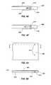
- FIG. 6Ais a partial side cross-sectional view of a microlens according to the present invention.
- FIG. 6Bis a partial side cross-sectional view of a microlens according to the present invention.
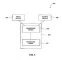
- FIG. 7shows a schematic block diagram of a system including a microlens array, including at least one microlens of the present invention.
- one or more semiconductor dicemay be at least partially encapsulated by application of a curable material thereabout and subsequent bulk or en masse hardening or curing thereof. More particularly, one or more semiconductor dice may be disposed upon a carrier and a package material (also termed an encapsulant), such as, for instance, a photopolymer, may be disposed about the periphery of the semiconductor dice and cured substantially in bulk or en masse. Subsequent to hardening or curing, the package material may be patterned, if necessary, to expose contact or bond pads of the semiconductor dice. Conductive traces and surface mount components may be disposed or formed as desired during or after the hardening of the package material. Such a configuration may eliminate the need for expensive transfer molding equipment and may provide increased flexibility in manufacturing.
- FIG. 1Ashows, in a perspective view, array 10 , which includes a plurality of semiconductor dice 12 disposed on a carrier 14 and arranged on the upper surface 16 thereof.
- Semiconductor dice 12may comprise known good dice, which have been tested to indicate at least a selected level of functionality. However, the use of known good dice is not limiting of the present invention.
- Carrier 14may comprise a solid substrate, such as a wafer or other bulk substrate blank, a tape or film, or a printed circuit board (PCB) substrate.
- PCBprinted circuit board
- semiconductor dice 12may be placed onto the upper surface 16 of carrier 14 by way of precision pick and place machinery, as known in the art.
- recessesmay be formed into the upper surface 16 of carrier 14 to facilitate placement, retention, or placement and retention of semiconductor dice 12 .
- a wafermay be diced to form semiconductor dice 12 , each of which may be affixed to a flexible film (not shown) and then the flexible film may be stretched to form gaps between semiconductor dice 12 and then encapsulated as described in more detail hereinbelow.
- the flexible filmmay be affixed to the wafer prior to dicing, and dicing may extend through the wafer but not through the flexible film.
- each of semiconductor dice 12may include, on the active surface 19 thereof, contact or bond pads 18 for electrical connection and communication to other, higher-level components.
- FIG. 1Cdepicts a partial side cross-sectional view of the array 10 shown in FIG. 1B , including package material 20 disposed about semiconductor dice 12 . More particularly, package material 20 may comprise a photopolymer that is initially disposed about semiconductor dice 12 by way of immersing, dipping, spin-coating, printing (stencil or screen printing, or other printing deposition process as known in the art), or spraying.
- uncured package material 20 disposed about semiconductor dice 12may exhibit an upper surface that is free, meaning substantially free to deform or be shaped according to the internal cohesive forces thereof.
- a retaining wall 25 that extends vertically along the outer periphery of carrier 14 , at least to the upper surface 21 of package material 20may be desirable to capture or retain uncured package material 20 disposed interstitially between semiconductor dice 12 .
- the package material 20may fill between and around the lateral peripheries of semiconductor dice 12 of array 10 as shown in FIG. 1C .
- package material 20comprises a photo-curable polymer, or “photopolymer,” curing or hardening may occur in response to exposure to light in the ultraviolet (“UV”) wavelength range.
- package material 20may comprise a photopolymer as known in the art, such as, for instance, commercially available photopolymers for use in stereolithography systems are available from Ciba Specialty Chemicals Inc. In addition, commercially available photopolymers for use in stereolithography systems are available from RPC, Ltd. of Marly, Switzerland, a wholly owned subsidiary of 3D Systems Corporation.
- package material 20may be preferably dielectric, so as to electrically insulate the semiconductor die as well as any conductive traces that may communicate therewith.
- package material 20may initially be uncured, i.e., a liquid, which may be at least partially cured subsequent to disposing about the periphery of each of semiconductor dice 12 .
- Package material 20 extending between semiconductor dice 12may be hardened or cured substantially en masse or substantially as a whole in response to exposure to a UV light or heat.
- curing of package material 20may be effected substantially en masse or substantially as a whole subsequent to deposition thereof by broad-source UV light in a chamber, thermal cure in an oven, microwave cure, or a combination thereof. In this manner, relatively thick, or deep, sections of package material 20 may be formed in a minimal amount of time.
- the formation of relatively thick sections or regions of hardened or cured package material 20 substantially en masse or substantially as a wholemay be advantageous in reducing, if not eliminating repeated scanning, of layer by layer regions of uncured package material dispersed between and around semiconductor dice 12 by way of traversing a focused laser beam to at least partially cure the same as may be required by conventional stereolithographic methods of encapsulation.
- curing the uncured package materialmay be performed selectively, i.e., excluding portions of uncured package material, or may occur in sequential steps, e.g., curing by UV light to form an initial structure, followed by oven heating or microwave curing to cure additional uncured package material.
- each of semiconductor dice 12may be at least partially surrounded or encapsulated by package material 20 to form packaged assembly 11 .
- Package material 20in combination with carrier 14 , may effect substantially complete semihermetic sealing of semiconductor dice 12 in relation to the areas surrounded therewith and may be formed thereabout in several ways, depending on the semiconductor dice 12 configurations and how semiconductor dice 12 are to be connected to higher-level packaging.
- upper surface 21 of package material 20may be substantially coplanar with active surfaces 19 of semiconductor dice 12 , as shown in FIG. 1C .
- Such a configurationmay allow for ease in forming electrically conductive traces extending from contact or bond pads 18 and may facilitate bulk curing of package material 20 , without additional apparatus and processes to prevent package material 20 from covering contact or bond pads 18 or to remove package material 20 therefrom, as explained in more detail hereinbelow.
- connection recesses 36may be formed by applying laminate structure 30 to the upper surface of packaged assembly 11 .
- Laminate structure 30may comprise dielectric upper layer 32 , dielectric lower layer 34 , and conductive traces 40 disposed therebetween.
- Laminate structure 30may preferably comprise a flex tape or TAB configuration, as known in the art, without limitation.
- Dielectric upper layer 32which is optional, may include apertures formed therein to expose a portion of conductive traces 40 that comprise connection recesses 36 .
- dielectric lower layer 34may include apertures formed therein to expose a portion of conductive traces 40 to form connection recesses 38 , by which, conductive traces 40 may be electrically connected to contact or bond pads 18 . Therefore, conductive traces 40 may extend from connection recesses 38 laterally outwardly to connection recesses 36 . Accordingly, connection recesses 38 may be sized and configured to align and electrically connect to contact or bond pads 18 of semiconductor dice 12 .
- laminate structure 30may be configured for communicating electrical signals between outer lead bonds (OLBs), i.e., connection recesses 36 and inner lead bonds (ILBs), i.e., the portion of conductive trace 40 connected to contact or bond pads 18 at connection recesses 38 .
- Dielectric lower layer 34may include an adhesive (not shown) for affixing laminate structure 30 to packaged assembly 11 . Further, such a configuration may inhibit moisture or contaminants from contacting contact or bond pads 18 of semiconductor dice 12 or the electrical connections thereto.
- a protective layer(not shown), instead of laminate structure 30 , may be disposed and adhesively affixed onto the active surfaces 19 of semiconductor dice 12 and the upper surface 21 of package material 20 .
- the protective layermay comprise a dielectric having apertures formed therein configured for depositing conductive material, such as, for instance, solder paste.
- Solder pastemay be deposited through a stencil mask (e.g., screen-printing or other printing technology as known in the art), or as otherwise known in the art and may be subsequently heated via a reflow oven or the like to form conductive traces 40 .
- semiconductor dice 12may be singulated to form packaged die 50 as shown in FIG. 1E .
- Solder balls 37as shown in broken lines, may be disposed or formed on connection recesses 36 , as desired, for connection with other devices or components.
- connection recesses 36as desired, for connection with other devices or components.
- packaged assembly 13may include package material 20 that extends over the active surfaces 19 of semiconductor dice 12 .
- package material 20may initially be uncured or flowable (i.e., a liquid) and may be at least partially cured or solidified substantially concurrently, substantially as a whole or en masse, subsequent to being disposed about the periphery of each of semiconductor dice 12 . Accordingly, package material 20 may be cured in response to exposure to a UV light or exposure to heat, e.g., curing of package material 20 by broad-source UV light, thermal cure, microwave cure, or combinations thereof. Accordingly, package material 20 covering semiconductor dice 12 may be cured in minimal time.
- contact or bond pads 18may be surrounded or covered by cured package material 20 , a photoresist resist application followed by a mask and etch process may be performed to remove the hardened material 20 disposed thereabove. Accordingly, in order to pattern the package material 20 , a photoresist resist layer (not shown) may be formed and patterned over the package material 20 surrounding or otherwise laterally adjacent to the contact or bond pads 18 , to protect the package material thereunder while the exposed package material 20 superimposed above the contact or bond pads 18 may be removed by, for instance, an etching process. Subsequently, photoresist resist layer (not shown) may be removed (stripped), as known in the art, leaving the remaining patterned package material 20 with contact or bond pads 18 exposed through apertures 23 ( FIG. 1G ).
- FIG. 1Hshows the packaged assembly 13 of FIG. 1G , but also including conductive traces 60 , wherein conductive traces 60 may be formed by CVD processes, cold-metal deposition processes, plating processes, or other conventional additive techniques in combination with photoresist application, masking, and etching processes for forming metal conductive circuit elements. Also, it should be noted that the conductive traces 60 might be formed by way of conductive paste deposited through a stencil mask, as described above.
- conductive traces 60may be formed by way of selective removal of copper (as by masking and etching) from a copper/dielectric laminate or by other conventional subtractive techniques. Conductive traces may be formed onto the active surfaces 19 of semiconductor dice 12 , over a portion of the vertical sidewall of packaging material 20 , and extending onto the upper surface 21 thereof.
- wire bondsmay extend from the contact or bond pads 18 of semiconductor dice 12 to conductive traces (not shown) formed on the upper surface 21 of package material 20 .
- Such a configurationmay be analogous to a lead-over-chip (LOC) type configuration.
- LOClead-over-chip
- conductive photopolymer materialsmay be used to form conductive traces 60 extending from contact or bond pads 18 of semiconductor dice 12 .
- conductive traces 60may be formed stereolithographically.
- a known photopolymermay be mixed with a conductive particle or a conductive precursor.
- conductive traces 60may initially comprise an uncured state, such as a liquid photopolymer having electrically conductive (e.g., a metal or a metal precursor) therein, where exposure to ultraviolet light or other subsequent processing may produce an at least partially cured conductive film.
- known photopolymersmay be mixed with silver. particles and at least partially cured to form conductive traces 60 .
- Commercially available photopolymers for use in stereolithography systemsare available from Ciba Specialty Chemicals Inc.
- Such conductive traces 60may be particularly suited to be used in combination with package material 20 , since both may be hardened by exposure to UV light or heat.
- the upper surface of package material 20may be cured, substantially as a whole, meaning across substantially the entire upper surface.
- conductive traces 60may be formed of conductive photopolymer materials and then the remaining uncured package material 20 , as well as the uncured conductive traces 60 , may be cured substantially as a whole.
- conductive traces 60may be formed according to a precision spray deposition process as disclosed in U.S. Pat. No. 6,251,488, as mentioned above.
- conductive traces 60may first be formed upon at least a portion of the upper surface 19 of semiconductor dice 12 , which has a substantially robust dielectric layer thereon, such as a spin-coated polymer. Then, packaging material 20 , such as a photopolymer, may be deposited in and around the conductive traces 60 and may be subsequently at least partially cured. The package material 20 may be selectively cured, substantially as a whole, to leave portions of conductive traces 60 exposed. Alternatively, package material 20 , which is cured and encapsulates conductive traces 60 , may be etched to expose a portion of conductive traces 60 therethrough.
- packaging material 20such as a photopolymer
- the packaging material 20may first be deposited and at least partially cured to form an arrangement that is suited for forming conductive traces 60 . Then, after conductive traces 60 are formed, the process for depositing and at least partially curing packaging material 20 may continue, including subsequent suitable processes for exposing at least a portion of conductive traces 60 to form connection recesses 36 . Such a configuration and process may form a substantially homogeneous packaging material 20 , with interstitial conductive traces 60 disposed therein and having connection recesses 36 . As yet a further alternative, conductive elements may be formed according to any of the methods of the present invention, which are disclosed hereinbelow.
- a packaged assembly 13 including conductive traces 60 fabricated according to the processes described in relation to any of the above-mentioned processesmay also be singulated between semiconductor dice 12 through package material 20 disposed therebetween to form a packaged die 80 , as shown in FIG. 11 .
- a dielectric layer 58comprising additional package material 20 or other dielectric material, may be deposited over the conductive traces 60 by processes known in the art. Such a configuration may seal against moisture or contaminants from contacting the electrical connections between conductive traces and contact or bond pads 18 of semiconductor dice 12 .
- Solder balls 37as shown in broken lines, may be formed onto connection recesses 36 , as desired, for connection with other devices or components.
- the package material 20may be formed to a suitable size and configuration to allow for such electrical components to be mounted to semiconductor dice 12 or package material 20 as so-called “surface mount” components.
- One or more surface mount componentsmay be installed after curing at least a portion of package material 20 about semiconductor dice 12 and, optionally, conductive traces may be formed before or after installation of surface mount components.
- Additional package material 20may be disposed about the one or more surface mount components and become cured thereafter.
- placement of surface mount componentsmay be performed via “pick and place” machinery, as known in the art.
- pick and place machinerymay be configured to install or position surface mount components suitably for operation with semiconductor dice 12 . It may be desirable to rinse the semiconductor dice 12 to remove any uncured package material therefrom, install any surface mount components, and return the semiconductor die 12 to the package material deposition equipment for continued application and at least partial curing of package material 20 .
- package material 20may include features configured for forming conductive vias, conductive traces, bond pads, or combinations thereof. Therefore, after disposal of uncured package material 20 about semiconductor dice 12 , UV light may be passed through an exposure mask, as known in photolithography, wherein the exposure mask is configured to selectively block or allow passage of the light therethrough.
- the exposure maskmay be configured so as to prevent UV light from interacting with uncured package 20 material proximate to the contact or bond pads 18 of the semiconductor dice 12 , and thus, not cure the same. Such a configuration may allow for increased flexibility in design of semiconductor dice 12 .
- geometrical featuresmay be formed by curing, en masse, a volume of uncured package material 20 , as through an exposure mask, and then changing the position of the free surface (upper surface) of the uncured package material, hardening a different area of uncured package material 20 , or a combination of both.
- Such a configurationmay provide for formation of repetitive topographical features in minimal time.
- subsequent heating or microwave curingmay be performed to effectively cure remaining uncured package material under a partially cured “skin” of photopolymer.
- the uncured package material proximate the contact or bond pads of the semiconductor dicemay preferably be removed, as by rinsing with a solvent or otherwise, prior to curing by heating.
- cover elementsmay be disposed adjacent to contact or bond pads and affixed to the active surfaces of semiconductor dice 12 prior to disposing uncured package material 20 about the periphery of semiconductor dice 12 .
- cover elementsmay be affixed to the active surfaces 19 of semiconductor dice 12 so as to seal against entry of the uncured package material 20 .
- barrier structuresmay be formed or applied so as to extend vertically from the active surfaces 19 of a semiconductor dice 12 about a periphery beyond the contact or bond pads 18 . The barrier structures may be formed so as to prevent uncured package material 20 from covering the contact or bond pads 18 of the semiconductor dice 12 so long as the uncured package material 20 height does not exceed the height of the barrier structures.
- FIG. 2Ashows cover elements 110 disposed upon semiconductor dice 12 of array 100 of the present invention, wherein cover elements 110 engage against the active surfaces 19 of semiconductor dice 12 so as to prevent package material 20 from covering contact or bond pads 18 .
- Cover elements 110may be preformed and pressed against active surfaces 19 , so as to seal thereagainst, or may be adhesively affixed thereto, so as to seal thereto.
- cover elements 110may be hardened substantially as a whole, formed onto the active surfaces 19 of semiconductor dice 12 , by way of selective exposure of package material 20 through an exposure mask.
- cover elements 110may be formed onto the active surfaces 19 of semiconductor dice 12 , as by, for instance, stereolithography.
- Cover elements 110may comprise polyimide, a cured photopolymer, a rubber, or an elastomer. Such materials may provide the ability to seal against the active surfaces 19 of semiconductor dice 12 .
- Uncured package material 20may be disposed about semiconductor dice 12 , as shown in FIG. 2B , showing array 101 .
- Uncured package material 20may extend vertically along the sidewall of cover elements 110 , or may be substantially coplanar with the active surface 19 of semiconductor dice 12 , without limitation.
- package material 20may be cured substantially in response to exposure to a UV light or heat, e.g., curing of package material 20 by broad-source UV light in a chamber, thermal cure in an oven, microwave cure, or a combination thereof, as described above. If UV light is used, the cover elements 110 may prevent curing of any package material 20 that, although unintended, becomes disposed between the cover element 110 and the contact or bond pads 18 by way of physically blocking the UV light.
- cover elements 110may be removed from engagement with active surfaces 19 of semiconductor dice 12 to form assembly 103 , as shown in FIG. 2C , so that the volumes or spaces previously occupied by cover elements 110 form apertures 116 , which may be configured to allow formation of conductive traces (not shown) as described above in relation to FIGS. 1D and 1H .
- FIG. 3Ashows barrier structures 130 disposed upon semiconductor dice 12 of assembly 10 of the present invention, wherein barrier structures 130 engage against the active surfaces 19 of semiconductor dice 12 so as to prevent package material 20 from covering contact or bond pads 18 .
- Barrier structures 130may form a continuous wall that forms an aperture 131 along its interior and may comprise polyimide, a cured photopolymer, a rubber, or an elastomer. Also, barrier structures 130 may be preformed and pressed against active surfaces 19 , so as to seal thereagainst, or may be adhesively affixed thereto, so as to seal thereagainst. Alternatively, barrier structures 130 may be formed onto the active surfaces 19 of semiconductor dice 12 , cured substantially as a whole or as by stereolithography techniques.
- package material 20may be disposed about semiconductor dice 12 , as shown in FIG. 3B .
- Uncured package material 20may extend vertically along the sidewall of barrier structures 130 , but may be prevented from contact with contact or bond pads 18 , so long as the vertical level of package material 20 does not exceed the upper surface of barrier structures 130 .
- uncured package material 20may be disposed substantially coplanar with or even vertically lower than the active surface 19 of semiconductor dice 12 so that the barrier structures 130 are merely to make certain that uncured package material 20 does not cover contact or bond pads 18 of semiconductor dice 12 , without limitation.
- Package material 20may be at least partially cured in response to exposure to a UV light, heat, microwave e.g., at least partially curing package material 20 by broad-source UV light in a chamber, thermal cure in an oven, microwave cure, or combinations thereof, as described above.
- barrier structures 130may be removed from active surfaces 19 of semiconductor dice 12 , or, alternatively, may remain on the active surfaces 19 of semiconductor dice 12 and may be reduced in height to be substantially coplanar with the upper surface 122 of package material 20 , by way of, for instance, planarizing the barrier structures 130 .
- encapsulation of a semiconductor die according to the present inventionmay form recesses for conductive traces.
- cover elements 29 A and 29 Bmay be positioned in an alternating fashion, extending from a respective contact or bond pad 18 of each of the semiconductor dice 12 laterally outwardly therefrom (in different directions as shown in FIG. 3C ) and engaging against the active surfaces 19 of semiconductor dice 12 , so as to prevent package material 20 from covering contact or bond pads 18 .
- Cover elements 29 A and 29 Bmay comprise polyimide, a cured photopolymer, a rubber, an elastomer, or another material exhibiting the ability to seal against the active surfaces 19 of semiconductor dice 12 .
- a forcemay be applied to the cover elements 29 A and 29 B generally toward the active surfaces 19 of each of semiconductor dice 12 to facilitate forming or maintaining a seal thereagainst.
- uncured package material 20may be disposed about semiconductor dice 12 and package material 20 may be cured en masse as described above. If UV light is used, the cover elements 29 A and 29 B may prevent curing of any package material 20 that may unintentionally become disposed between the cover elements 29 A or 29 B and the contact or bond pads 18 by physically blocking the UV light. Accordingly, referring to FIG.
- cover elements 29 A and 29 Bmay be removed from engagement with active surfaces 19 of semiconductor dice 12 and semiconductor dice 12 may be singulated to form a packaged die 111 , shown in a perspective view, wherein the spaces previously occupied by cover elements 29 A and 29 B, respectively, form recesses 33 A and 33 B, which may be structured for formation of conductive traces, bond pads, or both therein for providing electrical communication with bond or contact pads 18 of each of semiconductor dice 12 .
- package material 20may be formed about each of a plurality of semiconductor dice 12 ( FIG. 1 ) in two portions, 20 A and 20 B.
- portion 20 A of package material 20may be formed by the process described above, with respect to FIGS. 1B and 1C for forming encapsulation substantially to the active surface 19 of semiconductor dice 12 , or surrounding a portion of semiconductor dice 12 as otherwise desired.
- Portion 20 A of package materialmay be cured substantially en masse.
- Portion 20 B of package material 20may be formed stereolithographically (i.e., layer by layer), as described in U.S. Pat. No.
- portion 20 Bmay be formed as described with respect to FIGS. 3C and 3D , to provide relative flexibility in modifying or selecting the configuration of recesses 33 A and 33 B.
- Each of semiconductor dice 12may be diced or singulated after forming portion 20 A, after forming portion 20 B, or after forming both portion 20 A and portion 20 B, to form a package 113 as shown in FIG. 3E .
- each of the plurality of singulated semiconductor dicemay be positioned within a tray or upon another substrate for forming the other portion ( 20 A or 20 B) as desired.
- the present inventioncontemplates performing or causing substantially en masse curing of uncured package material about one or more semiconductor dice. Curing the package material substantially as a whole may occur so as to leave the contact or bond pads of the one or more semiconductor dice exposed, or may occur so that subsequent removal of a portion of cured package material may be required to expose the contact or bond pads of the semiconductor dice.
- packaging method of the present inventionmay be applied, by way of example and not limitation, to an unpackaged die, a die mounted to a lead frame (having a die mounting paddle or in a paddle-less leads-over-chip (LOC) or in a leads-under-chip (LUC) configuration), mounted to a carrier substrate in a chip-on-board (COB) or board-on-chip (BOC) arrangement, or in other packaging designs, as desired.
- a lead framehaving a die mounting paddle or in a paddle-less leads-over-chip (LOC) or in a leads-under-chip (LUC) configuration
- LOCleads-under-chip
- COBchip-on-board
- BOCboard-on-chip
- conductive elementsmay be formed upon a substrate or chip-scale package (CSP) by forming an organometallic layer over substantially an entire surface, as by application of a liquid and drying, if necessary, and then selectively processing the applied organometallic layer to form conductive traces. More particularly, in one embodiment, selectively exposing at least a portion of the organometallic layer to a heat source, such as a laser beam, may concentrate or form the metallic constituents therein sufficiently to form a conductive element. Alternatively, selective exposure of the organometallic layer to a laser beam may form a seed layer for forming a metal trace thereon by electrolytic processes, electroless processes, or other plating processes.
- CSPchip-scale package
- conductive traces 218 , conductive via 214 , and terminal pads 216may be formed by first applying an organometallic layer 220 to substantially the upper surface 217 of substrate 222 followed by selective patterning thereof.
- Organometallic layer 220may initially comprise a powder or a liquid, such as a polymer having metal, metallic compounds, or metal precursors therein, which may be subsequently dried and exposed to heat, a controlled atmosphere, or both heat and a controlled atmosphere may produce a metallic film or metallic seed layer.
- Emulsitone palladiumpalladiumfilm
- Emulsitone platinumplatinum
- an organometallic layer 220may be applied to at least a portion of the surface of substrate 222 by spin-coating, spraying, immersing, dipping, printing, or as otherwise known in the art.
- Portions of the organometallic layer 220may be selectively exposed to a laser beam, under a controlled atmosphere, such as forming gas (e.g., a mixture of about 90-95% nitrogen and 5-10% hydrogen), if necessary, to cause the organometallic layer 220 to chemically convert, concentrate, or otherwise remove organic constituents therefrom and to form a metallic film or seed layer.
- a controlled atmospheresuch as forming gas (e.g., a mixture of about 90-95% nitrogen and 5-10% hydrogen)
- forming gase.g., a mixture of about 90-95% nitrogen and 5-10% hydrogen
- platinum or palladiummay oxidize at elevated temperatures
- use of a forming gas or other oxidation inhibiting atmospheremay facilitate formation of a suitable metallic film or metallic seed layer.
- beam power, pulse rate, melting temperature of the organo-metallic layer 220as well as other process influencing parameters may be desirable or necessary for causing the organo-metallic layer 220 to form a metallic film or metallic seed layer.
- organometallic layer 220may comprise a particulate that is disposed over substantially the surface onto which conductive traces 218 , terminal pads 216 , or both are desired to be formed. Such a configuration may eliminate the need for a solvent to be used to remove an initial liquid or semiliquid layer that is dried upon a surface. If the exposed organometallic layer 220 forms a seed layer, electrolytic processes, electroless processes, or other plating processes may be used to deposit metal thereon to form conductive traces 218 and terminal pads 216 .
- portions thereofmay be selectively exposed to a laser beam to form a metallic film.
- the remaining unexposed or partially exposed organometallic layer 220may be dissolved or washed away by a solvent, such as isopropyl alcohol.
- a solventsuch as isopropyl alcohol.
- the exposed metallic filmmay be used directly as conductive traces 218 or terminal pads 216 .
- the exposed metallic filmmay be used as a seed layer for forming subsequent electroless or electroplated metal layers thereon to form conductive traces 218 or terminal pads 216 .
- via holes 215may be filled by repeated formation of sequentially stacked organometallic layers 225 therein, if necessary, with associated repeated exposure to a laser beam or other heat source, under a controlled atmosphere or independent thereof.
- the conductive via 214may comprise an organometallic material that may be selectively heated to form a conductive film 231 therein having a bore therethrough, as shown in FIG. 4F . Selective heating may be generated by a laser beam impinging upon organometallic material proximate via hole 215 .
- conductive via 214may comprise a conductive film formed on the boundary or side wall of the via holes 215 by way of selectively heating the organometallic material within via hole 215 .
- at least one subsequently formed electroless or electroplated metal layermay be formed upon a conductive film 231 .
- the conductive via 214may extend entirely through substrate 222 or may be a so-called “blind hole” (i.e., only partially through substrate 222 ), as known in the art.
- conductive via 214may be formed conventionally.
- FIGS. 4E and 4Falso show that an additional organometallic layer 220 may be applied to the opposing surface of the substrate 222 .
- Such a configurationmay be suited for forming different terminal pad 216 configurations (i.e., redistributing the electrical contacts) on the opposing sides of a substrate 222 .
- additional conductive traces(not shown) may be formed on the backside 219 of substrate 222 as well, by selective heating and removal of at least a portion of the organometallic layer 220 , as described hereinabove.
- substrate 222may comprise a rigid or flexible substrate.
- substrate 222may comprise a polyimide dielectric layer.
- the thickness of a substrate 222 comprising a polyimide dielectric layermay determine its flexibility. Accordingly, the present invention contemplates that the method for forming a conductive element of the present invention may encompass substrates that are relatively rigid, such as printed circuit board substrates, as well as relatively flexible substrates, such as those used in TAB, or substrates that are intermediate in flexibility, without limitation.
- conductive elementsmay be formed upon a substrate 322 by applying a conductive photopolymer or metal powder in a metallic layer 320 to substantially the upper surface 317 of a substrate 322 and then selectively processing the applied metallic layer 320 to form conductive traces 318 , terminal pads 316 , or combinations thereof.
- metallic layer 320may be selectively patterned by performing a resist and etch process in relation thereto to form conductive traces 318 , terminal pads 316 , or combinations thereof.
- conductive traces 318 , conductive vias 314 , and terminal pads 316may be formed by first applying an uncured metallic layer 320 to substantially the upper surface 317 of substrate 322 followed by selective patterning thereof.
- substrate 322may comprise a rigid or flexible substrate.
- substrate 222may comprise a polyimide, FR4, or ceramic material, without limitation.
- Metallic layer 320may initially comprise an uncured state, such as a liquid photopolymer having electrically conductive (e.g., metal or metal precursors) constituents therein, where exposure to ultraviolet light or other subsequent processing may produce an at least partially cured conductive film.
- metallic layer 320may comprise an initially uncured metal powder or metallic paste that may be at least partially cured responsive to exposure to ultraviolet light or heat.
- U.S. patent application No. 20020176793 of Moussa et al.discloses a metallic paste for use in stereolithography equipment.
- other commercially available photopolymer resinsmay be obtained from 3D Systems Inc. of Valencia, Calif.
- Metallic layer 320may be applied to substantially the surface of substrate 322 by spin-coating, spraying, or as otherwise known in the art.
- a resist layer(not shown) may be formed thereover and an etching process may be used to remove the portion of the cured metallic layer 320 that resist layer is not formed over. Then, resist layer may be removed (stripped), which leaves remaining patterned metallic layer 320 or, more specifically, conductive traces 318 and terminal pads 316 .
- resist layermay be removed (stripped), which leaves remaining patterned metallic layer 320 or, more specifically, conductive traces 318 and terminal pads 316 .
- conductive traces 318 and terminal pads 316may be formed upon the upper surface 317 of substrate 322 .
- via holes 315which may be formed by laser beam ablation, may be filled by repeated formation of sequentially stacked metallic layers 325 therein, as shown in FIG. 5E , if necessary, with associated repeated exposure to a UV light.
- the conductive vias 314may be substantially filled with an electrically conductive photopolymer and at least partially cured. Selective heating may be generated by a UV light impinging upon the upper surface 327 of conductive vias 314 , on the lower surface 329 of conductive vias 314 , or both.
- additional conductive tracesmay be formed on the backside 319 of substrate 322 in addition to conductive traces 318 formed on the upper surface 317 of substrate 322 by forming an additional metallic layer 320 on the opposing side surface of substrate 322 , as shown in FIG. 5E and patterning the additional metallic layer 320 as described hereinabove.
- At least one microlensmay be formed over or in proximity to a photosensor by stereolithography.
- stereolithography apparatusis known in the art and those of ordinary skill in the art will understand and appreciate that apparatus of other designs and manufacture, as well as modifications thereto, may be employed in practicing the method of the present invention.
- Stereolithographic apparatus and the operation thereofare described in great detail in United States Patents assigned to 3D Systems, Inc. of Valencia, Calif., such patents including, without limitation, U.S. Pat. Nos.
- stereolithography resinsthat exhibit suitable optical transparency (after formation) may be employed for forming a microlens according to the present invention.
- one particular stereolithography resin or photopolymer that may be used in accordance with the present inventionincludes Somos® 10120 WaterClearTM from DSM Desotech of the Netherlands.
- thermal stereolithography apparatusesAdditional apparatuses that may be useful in implementing the methods of the present invention, referred to as thermal stereolithography apparatuses, are described in great detail in United States Patents assigned to 3D Systems, Inc. of Valencia, Calif., such patents including, without limitation, U.S. Pat. Nos. 5,141,680; 5,344,298; 5,501,824; 5,569,349; 5,672,312; 5,695,707; 5,776,409; 5,855,836. The disclosure of each of the foregoing patents is hereby incorporated in its entirety herein by this reference.
- Exemplary commercially available thermal stereolithography apparatusoperating generally in the manner as that described above may include, but are not limited to, the THERMOJET® printer offered by 3D Systems, Inc., of Valencia, Calif.
- THERMOJET® printeroffered by 3D Systems, Inc., of Valencia, Calif.
- optically transparent thermoplastic materials, or “thermopolymers,”may be suitable for use in practicing the method of the present invention.
- the present inventionalso encompasses formation of a microlens comprising a photopolymer or thermopolymer material that exhibits suitable optical transparency (after formation) in combination with stereolighography apparatuses or according to other methods and processes.
- a suitable optically transparent photopolymer or thermoplasticmay be deposited for forming a microlens by way of so-called “maskless mesoscale materials deposition” (M3D). Such deposition may be selectively controlled, so that the optically transparent photopolymer or thermoplastic forms a desired shape or occupies a desired position.
- a materialmay be aerosolized by using an ultrasonic transducer or a pneumatic nebulizer. Then, the aerosol stream may be focused using a flow guidance deposition head, which forms an annular, co axial flow between the aerosol stream and a sheath gas stream. Further, patterning may be accomplished by moving the substrate or deposition head relative to one another. The optically transparent photopolymer or thermoplastic may be subsequently heated or selectively cured to consolidate the optically transparent photopolymer or thermoplastic, if necessary or desired.
- Commercially available maskless mesoscale materials deposition apparatusare produced by Optomec of Albuquerque, N.M.
- micropen deposition technologyor similar type deposition technologies, as known in the art, may be used for forming a microlens according to the present invention.
- a suitable optically transparent photopolymer or thermoplasticmay be deposited for forming a microlens by way of so-called micropen.
- Such depositionmay be selectively controlled, so that the optically transparent photopolymer or thermoplastic forms a desired shape occupies a desired position, or both.
- the optically transparent photopolymer or thermoplasticmay be subsequently heated or selectively cured to consolidate the optically transparent photopolymer or thermoplastic, if necessary or desired.
- MicroPenTM technologyis a direct writing method for patterning flowable materials with high precision through a controlled dispensing system.
- Commercially available MicroPenTM deposition apparatusare produced by OHMCRAFT, Inc. of Honeoye Falls, N.Y.
- a suitable optically transparent photopolymer or thermoplasticmay be deposited for forming a microlens by way of stamping technologies (which may also be known as microcontact printing technology), as known in the art, without limitation.
- a transfer diemay be provided and may have a surface thereof including optically transparent photopolymer or thermoplastic. Further, the surface of the transfer die may directly contact a substrate so as to deposit at least a portion of the optically transparent photopolymer or thermoplastic onto the surface of the substrate.
- the optically transparent photopolymer or thermoplasticmay be subsequently heated or selectively cured to consolidate the optically transparent photopolymer or thermoplastic, if necessary or desired.
- a suitable optically transparent photopolymer or thermoplasticmay be deposited by way of so-called 3-D printing technology, as known in the art, without limitation.
- 3-D printing technologycommercially available from Objet Geometries Ltd. of Rehovot, Israel, is the Eden 330®.
- the Eden 330®deposits photopolymer material via inkjet-type printer heads onto a support or other desired surface.
- photopolymeras thin as 16 ⁇ m and at a 600 ⁇ 300 dpi (dot per inch) resolution may be deposited in a selected location using the printer heads currently available.
- an ultraviolet (UV) lightmay be used to cure and harden each layer.
- the deposition processis repeated by selectively depositing additional photopolymer, followed by subsequent curing until a desired, three-dimensional structure (e.g., a computer-generated solid model or computer-aided design) is formed.
- 3-D printing systems and methodsare described in detail in U.S. Pat. Nos. 6,658,314; 6,644,763; 6,569,373; and 6,259,962 assigned to Objet Geometries Ltd., the disclosure of each of which is hereby incorporated, in its entirety, by reference herein. Further methods and apparatus related to 3-D printing technology are described in detail in U.S. Patent Applications 20020171177 A1 to Kritchman et al. and 20030151167 A1 to Kritchman et al., the disclosure of each of which are incorporated, in their entirety, by reference herein.
- FIG. 6Ashows a schematic partial side cross-sectional view of a portion of an array 410 of pixel sensors 428 , particularly depicting one pixel sensor 428 of the array 410 .
- each pixel sensor cell 428may include a photosensor 434 , which may be a photodiode, photogate, or the like, as known in the art.
- photosensormay comprise a photogate semitransparent conductor 466 , which is patterned.
- Source region 436 , drain region 440 , doped region 452 , gate stack 442 formed onto insulating layer 456 , gate stack 454 formed onto insulating layer 456 , and gate oxide layer 457may be configured to form one or more transistors, which may be controllable by electrical signals, as known in the art, wherein the signals may be used to operate the pixel sensor cell 428 .
- an applied control signalmay be communicated to the photosensor 434 so that when incident radiation 500 in the form of photons strikes the photosensor 434 , the photo-generated electrons accumulate in the source region 436 under the photosensor 434 .
- Field oxide regions 464may isolate the pixel cell 428 shown in FIG. 6A from other pixel sensors 428 in the array 410 .
- Protective layer 424may be formed over the supporting electrical elements and circuits mentioned above as well as photosensor 434 .
- Spacer layer 425may be formed prior to formation of microlens 422 and its thickness may be selected such that the photosensor 434 element may be preferably disposed generally proximate a focal point of radiation 500 traveling through microlens 422 .
- microlens 422may be fabricated by stereolithography techniques and apparatus. In one embodiment, microlens 422 may be fabricated directly. Specifically, as shown in FIG. 6B microlens 422 may be formed of a plurality of superimposed, mutually adhered layers 412 of material. As noted above suitable materials for stereolithography may include photopolymers and thermoplastics, without limitation. Although layers 412 of microlens 422 are shown in FIG. 6B as being separate, such representation is merely for facilitating understanding for the reader. It should be understood that layers 412 of microlens 422 may form a suitably optically transparent volume that may be used to refractively direct or focus radiation (not shown) toward photosensor 434 .
- microlens 422may be relatively small, for instance, about 1 or 2 ⁇ m, conventional stereolithography apparatus and methods may require modification, such as miniaturization of the laser beam focal spot size and layer material deposition techniques to perform suitable stereolithographic processes for forming microlens 422 .
- each of layers 412includes a substantially vertical side wall 413 , the existence of which, depending on the layer thickness in relation to the overall thickness of the structure being fabricated, causes the outer side surfaces of microlens 422 to be rough or stepped.
- This phenomenonis well-known in the art, the overall effect of mutually adjacent layers with differing positioned substantially vertical walls being termed “stair-stepping.” As the ability to form thinner layers increases, stair-stepping may be mitigated. Extrapolating even further, if the ability to form thin layers is advanced so that microlens 422 may comprise hundreds or thousands of mutually superimposed layers, the domed or arcuate surface thereof may be sufficiently smooth after stereolithographic formation of same.
- microlens 422may adequately focus or direct light toward the photosensor 434 despite the presence of stair-stepping, or at some magnitude of stair-stepping or layer thickness.
- stereolithographically formed microlens 422may be reflowed to cause the material thereof to form an arcuate upper surface.
- microlens 422may be chemically or mechanically processed to smooth the outer surface thereof. Particularly, brief exposure to a solvent or etching environment may tend to round the sharp corners of layers 412 .
- micromachining, as with a laser beam,may be used to round the comers of layers 412 . Any of such processes or combinations thereof may be used to smooth stair-stepped features of microlens 422 .
- FIG. 7shows a schematic block diagram of system 530 according to the present invention.
- Microlens array 510may be included in imaging device 520 , such as a CMOS imager, the imaging device including a processor device 532 , such as a central processing unit or other logic device, operably coupled thereto.
- Microlens array 510may include at least one microlens according to the present invention as described above.
- processor device 532may also be coupled with one or more appropriate input devices 534 (e.g., mouse, push-button, touch screen, communication interface, hard drive, etc.) and one or more output devices 536 (e.g., a display, printer, communication interface, hard drive, etc.) within system 530 .
- input devices 534e.g., mouse, push-button, touch screen, communication interface, hard drive, etc.
- output devices 536e.g., a display, printer, communication interface, hard drive, etc.
- the microlens array 510maybe utilized in various computing environments, systems, and devices, such as, for example, cell phones, personal data assistants (PDAs), and other similar electronic devices.
Landscapes
- Engineering & Computer Science (AREA)
- Manufacturing & Machinery (AREA)
- Microelectronics & Electronic Packaging (AREA)
- Chemical & Material Sciences (AREA)
- Materials Engineering (AREA)
- Physics & Mathematics (AREA)
- Condensed Matter Physics & Semiconductors (AREA)
- General Physics & Mathematics (AREA)
- Computer Hardware Design (AREA)
- Power Engineering (AREA)
- Encapsulation Of And Coatings For Semiconductor Or Solid State Devices (AREA)
Abstract
Description
- This application is a divisional of application Ser. No. 10/934,109, filed Sep. 2, 2004, pending.
- 1. Field of the Invention
- The present invention relates to semiconductor devices and components. Particularly, the present invention relates to at least partially packaging a semiconductor die or dice. The present invention also relates to forming conductive elements such as traces, vias, and bond pads. In addition, the present invention relates to a microlens for directing light toward a photosensor, methods of forming same, and systems so equipped.
- 2. Background of Related Art
- The invention pertains to a method for sealing and protecting at least the periphery of one or more semiconductor dice. When a semiconductor die is conductively attached to a carrier substrate, conventionally encapsulating the assembly is very desirable to enhance the mechanical bond between the die and the substrate and to mutually laterally electrically isolate adjacent electrical connections therebetween. More specifically, one common configuration for electrically connecting a semiconductor die is a so-called flip-chip package, wherein an array or pattern of external conductive elements, such as solder bumps or conductive or conductor-filled epoxy pillars, protrude from the active surface of the semiconductor die for use in mechanically and electrically connecting the semiconductor die to like-patterned ends of conductive traces of higher level packaging, such as a carrier substrate. Other semiconductor die configurations may include a die mounted to a lead frame (having a die mounting paddle configuration, or in a paddle-less leads-over-chip (LOC) configuration, or in a leads-under-chip (LUC) configuration) and, optionally, mounted to a carrier substrate in a chip-on-board (COB) or board-on-chip (BOC) arrangement, or in other packaging designs, as desired.
- Conventional encapsulation typically involves transfer molding an encapsulant, usually a particulate silica filled thermoset, to substantially surround a semiconductor die electrically connected and mechanically affixed to a carrier substrate. Transfer molds typically comprise a bottom mold and an upper mold, wherein the mold halves may be mated to one another to form a plurality of predefined cavities, wherein usually one predefined cavity receives one of a plurality of semiconductor dice. Each semiconductor die may be placed within the cavity and encapsulant may be forced into each of the plurality of cavities to form an encapsulation structure that encapsulates the semiconductor chip and portions of the lead frame or carrier substrate.
- In operation, a heated, silica-filled resin mold compound, usually a thermoset, is heated to a molten state, forced under pressure through runners into and through the mold cavities, wherein semiconductor die assemblies comprising semiconductor dice with attached lead frames or substrates are disposed (usually in strips or other groups, so that a group of six semiconductor dice, for example, would be placed in and across six cavities formed by the molds). After molding, the encapsulated semiconductor die assemblies may be ejected from the cavities by ejector pins, after which they may be post-cured at an elevated temperature to complete cross-linking of the resin mold compound, followed by other operations as known in the art. It will be appreciated that other transfer molding apparatus configurations, as well as variations in the details of the described method, are known in the art.
- Undesirably, encapsulant flow during conventional transfer molding within mold cavities is demonstrably nonuniform. Therefore, encapsulant filler particles may become lodged between lead ends and the underlying die surfaces because the flow characteristics of the viscous encapsulant flow may cause particles to be forcefully driven between the lead ends and the additional surfaces of the semiconductor die and wedged or jammed in place in low-clearance areas. As the encapsulant flow front advances and the mold operation is completed by packing the cavities, pressure in substantially all portions of the mold cavities may be substantially hydrostatic. With LOC arrangements, where lead ends extending over the active surface of a die are bonded thereto by adhesive-coated tape segments or an adhesive material patterned on the active surface, the relative inflexibility of the tightly-constrained (adhered) lead ends maintains the point stresses of any particles trapped under the lead ends. These residual stresses are carried forward in the fabrication process to post-cure and beyond. When mechanical, thermal or electrical stresses attendant to post-encapsulation processing are added to the residual stresses associated with the lodged filler particles, cracking or perforation of the die coat may occur. It has been observed that filler particle-induced damage may occur more frequently in close proximity to the adhesive, where lead flexibility is relatively low. In addition to damage by filler particles, transfer molding also results in the problem of bond wire sweep, wherein bond wires may be damaged, broken, or loosened from their connections to bond pads or lead ends, or swept into shorting contact with an adjacent bond wire under the impetus of the flow front of molten resin encapsulant as it flows through a mold cavity. Also, due to increased pressures exerted on the encapsulant, a small amount of the encapsulation material often may flash between the mold halves, which may interfere with handling or require removal.
- In addition to end-product deficiencies as noted above due to the phenomena of particulate die coat penetration, flash formation, and bond wire sweep, the capital-intensive nature of the transfer molding apparatus, including the requirement for different, relatively expensive molds for each die and lead frame or other substrate arrangement, as well as the high cost of the encapsulant resin and waste of same that is not used in the mold cavities, renders the transfer molding process an extremely expensive one. Mold damage and refurbishment is an additional, ongoing cost. Further, the elevated temperatures used in the molding process, as well as in the post cure of the resin encapsulant, are detrimental to the circuitry of the die as well as to the electrical connections to the lead ends.
- Accordingly, the prior art has developed nonmolding encapsulation techniques for surrounding and at least partially sealing semiconductor dice. For instance, U.S. Pat. No. 6,549,821 to Farnworth et al., assigned to the assignee of the present invention and the disclosure of which is incorporated in its entirety by reference thereto, discloses a method and apparatus for applying packaging material to workpieces, particularly electronic components including semiconductor dice.
- In addition, U.S. Pat. No. 6,537,482 to Farnworth, assigned to the assignee of the present invention and the disclosure of which is incorporated in its entirety by reference thereto, discloses a method for underfilling and encapsulating flip-chip configured semiconductor devices mounted on a carrier substrate using stereolithography to form at least semisolid dam structures of photopolymeric material to entrap unpolymerized resin between the devices and substrate.
- However, in either of the above-mentioned conventional stereolithography approaches to encapsulation of semiconductor dice, the need for forming a multitude of relatively thin layers stereolithographically may be time consuming and may also depend on precise placement of the semiconductor dice, or, alternatively, a vision system for detecting the position thereof. Thus, there remains a need for improved apparatus and methods for at least partially encapsulating semiconductor dice without performing transfer molding.
- Turning to another facet of conventional electronic fabrication techniques, conventional conductive traces may be formed by CVD processes, cold-metal deposition processes, plating processes, or other conventional additive techniques in combination with resist and etching processes, by way of solder paste deposited through a stencil, or by way of selective removal of copper from a copper dielectric laminate, as by masking and etching or other conventional subtractive techniques.
- In relation to semiconductor dice, tape automated bonding (TAB) is sometimes used to form an electrical connection between the unpackaged die and external circuitry on a circuit board or other substrate. A TAB tape includes a flexible film, such as polyimide, having circuit traces formed thereon. The circuit traces may include bumps that are adapted for electrical connection to the bond pads on a die. The bumps and the circuit traces on the TAB tape provide an electrical path from the bond pads of the semiconductor die to external circuitry.
- Also, circuit boards are often assembled with semiconductor devices to electrically connect different semiconductor devices to one another or to other components of an electronic device. Typically, circuit boards have one or more layers of metal circuitry carried by the insulating, or dielectric, substrates thereof. When circuit boards have conductive circuits extending across more than one plane thereof, the circuits may be electrically connected by way of through holes or blind holes that are metal plated or filled, which are known as conductive “vias.”
- U.S. Pat. Nos. 6,500,746 and 6,632,732 to Williams, each assigned to the assignee of the present invention and the disclosure of each of which is incorporated herein in its entirety, each discloses stereolithographically fabricated conductive elements that may be formed onto circuit boards or chip scale packages. The patents also disclose that conductive traces, bond pads, and conductive vias may be formed stereolithographically. Further, U.S. Pat. No. 6,251,488 to Miller et al. discloses a precision spray process wherein metal particles are propelled toward a surface and heated while in flight toward the surface by a laser beam.
- However, while the prior art methods may function as intended for forming conductive elements, there is a need for improved apparatus and methods for forming conductive elements, such as traces, bond pads, and conductive vias that are associated with electronic devices, such as circuit boards, or upon other substrates.
- Moving to a further aspect of the prior art, it is known in the art to use a microlens array in combination with an imager array, such as a CMOS imager array, wherein the microlens array comprises a convex microlens associated with each pixel or the CMOS imager. Each microlens is configured to refract incident radiation from the circuitry region of the pixel to the photosensor region of the CMOS imager, thereby increasing the amount of light reaching the photosensor and increasing the fill factor of the pixels. Other uses of microlens arrays may include intensifying illuminating light on the pixels of a nonluminescent display device, such as a liquid crystal display device to increase the brightness of the display, forming an image to be printed in a liquid crystal or light emitting diode printer and as a focusing structure for coupling a luminescent device or a receptive device to an optical fiber.
- Conventionally, a microlens or microlens array may be formed by depositing a microlens material layer by spin coating onto a surface of a semiconductor structure, in general alignment with a photosensor region thereof. The microlens areas may be patterned by a conventional photolithographic method, such as, for instance, a resist and etch process, and then may be subjected to increased temperature by a reflow process, for instance, at a temperature of about 160° Celsius. More specifically, the temperature may exceed the glass transition temperature of the microlens material, so that the upper surface area thereof forms an arcuate or domed surface, according to the surface tension or cohesive forces in the microlens material. A microlens may be formed of a transparent material exhibiting a suitable refractive index. For instance, a microlens may comprise an optical thermoplastic, such as polymethylmethacrylate, polycarbonate, polyolefin, cellulose acetate butyrate, polystyrene, or polyimide; a thermoset resin such as an epoxy resin; a photosensitive gelatin; or a radiation curable resin, such as acrylate, methacrylate, urethane acrylate, epoxy acrylate, or polyester acrylate.
- U.S. Pat. No. 6,307,243 to Rhodes, assigned to the assignee of the present invention and the disclosure of which is incorporated in its entirety by reference thereto, discloses a microlens array for use in a solid-state imager having an improved fill factor. More specifically, an insulation layer is formed of transparent insulating material, such as silicon oxide, silicon nitride, or silicon oxynitride, above each microlens in order to capture more light at the pixel edges and transmit such light to the photosensor, thereby improving the fill factor of the microlens array.
- However, there is a need for improved apparatus and methods for forming one or more microlens structures. Particularly, there is a need for improved apparatus and methods for forming one or more microlens structures that are associated with image arrays, such as CMOS imagers.
- In one aspect of the present invention, a plurality of semiconductor dice may be at least partially encapsulated or packaged by application of a flowable dielectric material thereabout and subsequent bulk or en masse hardening or curing thereof. More particularly, a plurality of semiconductor dice may be disposed upon a carrier and a package material, such as, for instance, a photopolymer, may be disposed about the periphery of the semiconductor dice and at least partially cured substantially en masse. The uncured material may be prevented from at least partially curing proximate to the contact or bond pads of the at least one semiconductor die. Alternatively, at least partially cured material may be removed to expose the contact pads of the at least one semiconductor die. Further, conductive traces may be formed on the package material, applied as TAB, or otherwise formed to facilitate electrically connecting the at least one semiconductor die to other, higher-level electrical components. Of course, a plurality of semiconductor dice may each be affixed to a carrier, at least partially encapsulated, and subsequently diced or singulated through the cured dielectric material to form a plurality of respective, individually-packaged semiconductor dice.
- In another aspect of the present invention, a method for forming a substrate that carries one or more conductive traces is disclosed. The conductive traces, bond pads, or vias of a substrate may be formed by depositing a layer of organometallic material, such as, for instance, Emulsitone palladium or platinum. The organometallic layer may be deposited in an uncured form, such as a liquid, with the metallic material or precursors dispersed therein. The organometallic layer may be dried, and then at least portions of the organometallic layer selectively heated, as by a laser beam, to consolidate the metallic particles and at least partially remove the organic compounds remaining in the organometallic layer. The substrate may, subsequent to selective heating, be rinsed with a solvent of suitable compatibility with an underlying substrate (e.g., isopropyl alcohol) to remove the uncured organometallic layer or organic material remaining in the exposed portion of the organometallic layer.
- Further, in another aspect of the present invention , a conductive element may be formed onto a substrate by depositing an uncured material onto a surface of a substrate, selectively at least partially curing the uncured material over at least a portion of the surface thereof, and removing a portion of the at least partially cured material. Particularly, a conductive photopolymer may be deposited over at least a portion of a substrate surface, at least partially cured, and then selectively removed to form conductive elements.
- Substrates upon or within which conductive elements are formed according to the present invention may be relatively rigid, such as printed circuit board substrates; relatively flexible, such as those used in TAB; or intermediate in flexibility, without limitation. Accordingly, substrates, including conductive elements of the present invention, may comprise a polyimide, FR4, or ceramic material.
- The present invention also contemplates a method of fabrication of a microlens for use in an imaging device. Specifically, a flowable, uncured optically transmissive material may be disposed onto a surface of a substrate and at least a portion thereof may be selectively at least partially cured. Further, the uncured optically transmissive material may be removed from the surface of the substrate. The uncured optically transmissive material may comprise a material with suitable optical characteristics, such as at least one of a photopolymer and a thermoplastic.
- The microlens may comprise one or more superimposed, mutually adhered layers. Also, an exterior surface of the microlens may exhibit stair-stepping. Alternatively, an exterior surface of the microlens may be formed to be relatively smooth by way of at least one of heating the microlens to a temperature exceeding a glass transition temperature thereof, micromachining with a laser beam, and exposing the microlens to a solvent.
- The present invention also contemplates a microlens for directing radiation toward a sensor of an imaging device comprising a plurality of mutually adhered layers of cured optically transmissive material.
- Other features and advantages of the present invention will become apparent to those of skill in the art through consideration of the ensuing description, the accompanying drawings, and the appended claims.
FIG. 1A is a perspective schematic representation of an array of individual, or singulated, semiconductor dice disposed on a carrier;FIG. 1B is a partial side cross-sectional view of the array shown inFIG. 1A , the cross-section taken along line3-3 and viewed generally from direction1;FIG. 1C is a partial side cross-sectional view of the array shown inFIG. 1B , wherein the semiconductor dice are partially encapsulated into an assembly and the encapsulating material is substantially coplanar with the active surfaces of the semiconductor dice;FIG. 1D is an exploded partial side cross-sectional view of the assembly shown inFIG. 1C , including a laminate structure for assembly therewith;FIG. 1E is a side cross-sectional view of a singulated die of the assembly shown inFIG. 1D after application of the laminate structure;FIG. 1F is a partial side cross-sectional view of the array shown inFIG. 1B , wherein the semiconductor dice are partially encapsulated into an assembly and the encapsulating material covers at least a portion of the active surfaces of the semiconductor dice;FIG. 1G is a side cross-sectional view of the assembly shown inFIG. 1F , after a photoresist, mask, and etch process is used to expose the contact pads of the semiconductor dice;FIG. 1H is a side cross-sectional view of the assembly shown inFIG. 1G , including conductive traces formed thereon;FIG. 1I is a partial cross-sectional view of a singulated die of the assembly shown inFIG. 1G ;FIG. 2A is a side cross-sectional view of an array of semiconductor dice including cover elements positioned over the contact pads thereof;FIG. 2B is a side cross-sectional view of the array shown inFIG. 2A , including encapsulating material disposed about the semiconductor dice to form an assembly;FIG. 2C is a side cross-sectional view of the assembly shown inFIG. 2B , but without cover elements;FIG. 3A is a side cross-sectional view of an array of semiconductor dice including barrier structures disposed on the active surfaces thereof;FIG. 3B is a side cross-sectional view of the array shown inFIG. 3A , including encapsulating material disposed about the semiconductor dice to form an assembly;FIG. 3C is a partial side cross-sectional view of an array of semiconductor dice including encapsulating material disposed about the semiconductor dice to form an assembly;FIG. 3D is a perspective view of a packaged die of the present invention;FIG. 3E is a perspective view of another packaged die of the present invention;FIG. 4A is a top elevation of a substrate of the present invention including an organometallic layer;FIG. 4B is a partial side cross-sectional view of the substrate shown inFIG. 4A ;FIG. 4C is a top elevation of the substrate shown inFIGS. 4A and 4B , wherein the organometallic layer has been patterned;FIG. 4D is a partial side cross-sectional view of the substrate shown inFIG. 4C ;FIG. 4E is an enlarged partial side cross-sectional view of a conductive via of the present invention extending through a substrate;FIG. 4F is an enlarged partial side cross-sectional view of a conductive via of the present invention extending through a substrate;FIG. 5A is a top elevation of a substrate of the present invention including a metallic layer disposed substantially over the upper surface of a substrate;FIG. 5B is a partial side cross-sectional view of the substrate shown inFIG. 5A ;FIG. 5C is a top elevation of the substrate shown inFIGS. 5A and 5B , wherein the metallic layer has been patterned;FIG. 5D is a partial side cross-sectional view of the substrate shown inFIG. 5C ;FIG. 5E is an enlarged partial side cross-sectional view of a conductive via of the present invention extending through a substrate;FIG. 6A is a partial side cross-sectional view of a microlens according to the present invention;FIG. 6B is a partial side cross-sectional view of a microlens according to the present invention; andFIG. 7 shows a schematic block diagram of a system including a microlens array, including at least one microlens of the present invention.- In one aspect of the present invention, one or more semiconductor dice may be at least partially encapsulated by application of a curable material thereabout and subsequent bulk or en masse hardening or curing thereof. More particularly, one or more semiconductor dice may be disposed upon a carrier and a package material (also termed an encapsulant), such as, for instance, a photopolymer, may be disposed about the periphery of the semiconductor dice and cured substantially in bulk or en masse. Subsequent to hardening or curing, the package material may be patterned, if necessary, to expose contact or bond pads of the semiconductor dice. Conductive traces and surface mount components may be disposed or formed as desired during or after the hardening of the package material. Such a configuration may eliminate the need for expensive transfer molding equipment and may provide increased flexibility in manufacturing.
FIG. 1A shows, in a perspective view,array 10, which includes a plurality ofsemiconductor dice 12 disposed on acarrier 14 and arranged on theupper surface 16 thereof.Semiconductor dice 12 may comprise known good dice, which have been tested to indicate at least a selected level of functionality. However, the use of known good dice is not limiting of the present invention.Carrier 14 may comprise a solid substrate, such as a wafer or other bulk substrate blank, a tape or film, or a printed circuit board (PCB) substrate. Each of the plurality ofsemiconductor dice 12 may be adhesively affixed tocarrier 14 in order to maintain the position of each ofsemiconductor dice 12 in relation toother semiconductor dice 12. For instance,semiconductor dice 12 may be placed onto theupper surface 16 ofcarrier 14 by way of precision pick and place machinery, as known in the art. Alternatively, or additionally, recesses (not shown) may be formed into theupper surface 16 ofcarrier 14 to facilitate placement, retention, or placement and retention ofsemiconductor dice 12.- In a further alternative, a wafer may be diced to form
semiconductor dice 12, each of which may be affixed to a flexible film (not shown) and then the flexible film may be stretched to form gaps betweensemiconductor dice 12 and then encapsulated as described in more detail hereinbelow. Optionally, the flexible film may be affixed to the wafer prior to dicing, and dicing may extend through the wafer but not through the flexible film. - As shown in
FIG. 1B , which depicts a partial side cross-sectional view of thearray 10 shown inFIG. 1A along reference line3-3, each ofsemiconductor dice 12 may include, on theactive surface 19 thereof, contact orbond pads 18 for electrical connection and communication to other, higher-level components.FIG. 1C depicts a partial side cross-sectional view of thearray 10 shown inFIG. 1B , includingpackage material 20 disposed aboutsemiconductor dice 12. More particularly,package material 20 may comprise a photopolymer that is initially disposed aboutsemiconductor dice 12 by way of immersing, dipping, spin-coating, printing (stencil or screen printing, or other printing deposition process as known in the art), or spraying. Thus,uncured package material 20 disposed aboutsemiconductor dice 12 may exhibit an upper surface that is free, meaning substantially free to deform or be shaped according to the internal cohesive forces thereof. As may be appreciated, a retainingwall 25 that extends vertically along the outer periphery ofcarrier 14, at least to theupper surface 21 ofpackage material 20, may be desirable to capture or retainuncured package material 20 disposed interstitially betweensemiconductor dice 12. Accordingly, thepackage material 20 may fill between and around the lateral peripheries ofsemiconductor dice 12 ofarray 10 as shown inFIG. 1C . - If
package material 20 comprises a photo-curable polymer, or “photopolymer,” curing or hardening may occur in response to exposure to light in the ultraviolet (“UV”) wavelength range. For instance,package material 20 may comprise a photopolymer as known in the art, such as, for instance, commercially available photopolymers for use in stereolithography systems are available from Ciba Specialty Chemicals Inc. In addition, commercially available photopolymers for use in stereolithography systems are available from RPC, Ltd. of Marly, Switzerland, a wholly owned subsidiary of 3D Systems Corporation. As one may appreciate,package material 20 may be preferably dielectric, so as to electrically insulate the semiconductor die as well as any conductive traces that may communicate therewith. - Accordingly,
package material 20 may initially be uncured, i.e., a liquid, which may be at least partially cured subsequent to disposing about the periphery of each ofsemiconductor dice 12.Package material 20 extending betweensemiconductor dice 12 may be hardened or cured substantially en masse or substantially as a whole in response to exposure to a UV light or heat. Put another way, curing ofpackage material 20 may be effected substantially en masse or substantially as a whole subsequent to deposition thereof by broad-source UV light in a chamber, thermal cure in an oven, microwave cure, or a combination thereof. In this manner, relatively thick, or deep, sections ofpackage material 20 may be formed in a minimal amount of time. - The formation of relatively thick sections or regions of hardened or cured
package material 20 substantially en masse or substantially as a whole may be advantageous in reducing, if not eliminating repeated scanning, of layer by layer regions of uncured package material dispersed between and aroundsemiconductor dice 12 by way of traversing a focused laser beam to at least partially cure the same as may be required by conventional stereolithographic methods of encapsulation. - It should be understood, however, that hardening or curing uncured package material, when described herein as occurring substantially as a whole, substantially en masse, or substantially in bulk, does not imply “instant” curing of the entire volume of uncured package material. Rather, the above-listed references refer to a condition, wherein the environmental condition that causes curing of the uncured package material applies to or influences a substantial portion or volume of the uncured package material at substantially the same time. Such a configuration may decrease the amount of time that is required to complete the desired curing. However, curing the uncured package material may be performed selectively, i.e., excluding portions of uncured package material, or may occur in sequential steps, e.g., curing by UV light to form an initial structure, followed by oven heating or microwave curing to cure additional uncured package material.
- Thus, as shown in
FIG. 1C , each ofsemiconductor dice 12 may be at least partially surrounded or encapsulated bypackage material 20 to form packagedassembly 11.Package material 20, in combination withcarrier 14, may effect substantially complete semihermetic sealing ofsemiconductor dice 12 in relation to the areas surrounded therewith and may be formed thereabout in several ways, depending on thesemiconductor dice 12 configurations and howsemiconductor dice 12 are to be connected to higher-level packaging. In particular,upper surface 21 ofpackage material 20 may be substantially coplanar withactive surfaces 19 ofsemiconductor dice 12, as shown inFIG. 1C . Such a configuration may allow for ease in forming electrically conductive traces extending from contact orbond pads 18 and may facilitate bulk curing ofpackage material 20, without additional apparatus and processes to preventpackage material 20 from covering contact orbond pads 18 or to removepackage material 20 therefrom, as explained in more detail hereinbelow. - Regarding the formation of conductive traces, as shown in
FIG. 1D , which depicts a partial side cross-sectional view ofassembly 31, connection recesses36 may be formed by applyinglaminate structure 30 to the upper surface of packagedassembly 11.Laminate structure 30 may comprise dielectricupper layer 32, dielectriclower layer 34, andconductive traces 40 disposed therebetween.Laminate structure 30 may preferably comprise a flex tape or TAB configuration, as known in the art, without limitation. Dielectricupper layer 32, which is optional, may include apertures formed therein to expose a portion ofconductive traces 40 that comprise connection recesses36. Likewise, dielectriclower layer 34 may include apertures formed therein to expose a portion ofconductive traces 40 to form connection recesses38, by which, conductive traces40 may be electrically connected to contact orbond pads 18. Therefore, conductive traces40 may extend from connection recesses38 laterally outwardly to connection recesses36. Accordingly, connection recesses38 may be sized and configured to align and electrically connect to contact orbond pads 18 ofsemiconductor dice 12. As may be appreciated,laminate structure 30 may be configured for communicating electrical signals between outer lead bonds (OLBs), i.e., connection recesses36 and inner lead bonds (ILBs), i.e., the portion ofconductive trace 40 connected to contact orbond pads 18 at connection recesses38. Dielectriclower layer 34 may include an adhesive (not shown) for affixinglaminate structure 30 to packagedassembly 11. Further, such a configuration may inhibit moisture or contaminants from contacting contact orbond pads 18 ofsemiconductor dice 12 or the electrical connections thereto. - Alternatively, a protective layer (not shown), instead of
laminate structure 30, may be disposed and adhesively affixed onto theactive surfaces 19 ofsemiconductor dice 12 and theupper surface 21 ofpackage material 20. The protective layer may comprise a dielectric having apertures formed therein configured for depositing conductive material, such as, for instance, solder paste. Solder paste may be deposited through a stencil mask (e.g., screen-printing or other printing technology as known in the art), or as otherwise known in the art and may be subsequently heated via a reflow oven or the like to form conductive traces40. - Additionally,
semiconductor dice 12 may be singulated to form packaged die50 as shown inFIG. 1E .Solder balls 37, as shown in broken lines, may be disposed or formed on connection recesses36, as desired, for connection with other devices or components. As may be appreciated by one of ordinary skill in the art, there are many alternative configurations for at least partially packaging one or more semiconductor dice according to the present invention. Also, there are many alternative configurations for exposing contact or bond pads covered by cured package material or preventing such coverage thereof and subsequent formation of conductive traces extending therefrom, according to the present invention. - For instance, in one alternative, as shown in
FIG. 1F , packagedassembly 13 may includepackage material 20 that extends over theactive surfaces 19 ofsemiconductor dice 12. As described above,package material 20 may initially be uncured or flowable (i.e., a liquid) and may be at least partially cured or solidified substantially concurrently, substantially as a whole or en masse, subsequent to being disposed about the periphery of each ofsemiconductor dice 12. Accordingly,package material 20 may be cured in response to exposure to a UV light or exposure to heat, e.g., curing ofpackage material 20 by broad-source UV light, thermal cure, microwave cure, or combinations thereof. Accordingly,package material 20 coveringsemiconductor dice 12 may be cured in minimal time. - Further, since contact or
bond pads 18 may be surrounded or covered by curedpackage material 20, a photoresist resist application followed by a mask and etch process may be performed to remove thehardened material 20 disposed thereabove. Accordingly, in order to pattern thepackage material 20, a photoresist resist layer (not shown) may be formed and patterned over thepackage material 20 surrounding or otherwise laterally adjacent to the contact orbond pads 18, to protect the package material thereunder while the exposedpackage material 20 superimposed above the contact orbond pads 18 may be removed by, for instance, an etching process. Subsequently, photoresist resist layer (not shown) may be removed (stripped), as known in the art, leaving the remaining patternedpackage material 20 with contact orbond pads 18 exposed through apertures23 (FIG. 1G ). - Thus, the contact or
bond pads 18 ofsemiconductor dice 12 may be exposed, throughapertures 23 to enable formation of associated conductive traces and bond pads. More particularly,FIG. 1H shows the packagedassembly 13 ofFIG. 1G , but also including conductive traces60, wherein conductive traces60 may be formed by CVD processes, cold-metal deposition processes, plating processes, or other conventional additive techniques in combination with photoresist application, masking, and etching processes for forming metal conductive circuit elements. Also, it should be noted that the conductive traces60 might be formed by way of conductive paste deposited through a stencil mask, as described above. Alternatively, conductive traces60 may be formed by way of selective removal of copper (as by masking and etching) from a copper/dielectric laminate or by other conventional subtractive techniques. Conductive traces may be formed onto theactive surfaces 19 ofsemiconductor dice 12, over a portion of the vertical sidewall ofpackaging material 20, and extending onto theupper surface 21 thereof. - Of course, wire bonds (not shown) may extend from the contact or
bond pads 18 ofsemiconductor dice 12 to conductive traces (not shown) formed on theupper surface 21 ofpackage material 20. Such a configuration may be analogous to a lead-over-chip (LOC) type configuration. - In another embodiment, conductive photopolymer materials may be used to form
conductive traces 60 extending from contact orbond pads 18 ofsemiconductor dice 12. Particularly, conductive traces60 may be formed stereolithographically. In one embodiment, a known photopolymer may be mixed with a conductive particle or a conductive precursor. For instance, conductive traces60 may initially comprise an uncured state, such as a liquid photopolymer having electrically conductive (e.g., a metal or a metal precursor) therein, where exposure to ultraviolet light or other subsequent processing may produce an at least partially cured conductive film. In a particular example, known photopolymers may be mixed with silver. particles and at least partially cured to form conductive traces60. Commercially available photopolymers for use in stereolithography systems are available from Ciba Specialty Chemicals Inc - Such conductive traces60 may be particularly suited to be used in combination with
package material 20, since both may be hardened by exposure to UV light or heat. For instance, the upper surface ofpackage material 20 may be cured, substantially as a whole, meaning across substantially the entire upper surface. Then,conductive traces 60 may be formed of conductive photopolymer materials and then the remaininguncured package material 20, as well as the uncured conductive traces60, may be cured substantially as a whole. As a further alternative,conductive traces 60 may be formed according to a precision spray deposition process as disclosed in U.S. Pat. No. 6,251,488, as mentioned above. - In yet another embodiment, conductive traces60 may first be formed upon at least a portion of the
upper surface 19 ofsemiconductor dice 12, which has a substantially robust dielectric layer thereon, such as a spin-coated polymer. Then, packagingmaterial 20, such as a photopolymer, may be deposited in and around the conductive traces60 and may be subsequently at least partially cured. Thepackage material 20 may be selectively cured, substantially as a whole, to leave portions ofconductive traces 60 exposed. Alternatively,package material 20, which is cured and encapsulatesconductive traces 60, may be etched to expose a portion ofconductive traces 60 therethrough. In other words, thepackaging material 20 may first be deposited and at least partially cured to form an arrangement that is suited for forming conductive traces60. Then, after conductive traces60 are formed, the process for depositing and at least partially curingpackaging material 20 may continue, including subsequent suitable processes for exposing at least a portion ofconductive traces 60 to form connection recesses36. Such a configuration and process may form a substantiallyhomogeneous packaging material 20, with interstitial conductive traces60 disposed therein and having connection recesses36. As yet a further alternative, conductive elements may be formed according to any of the methods of the present invention, which are disclosed hereinbelow. - Consequently, a packaged
assembly 13 including conductive traces60 fabricated according to the processes described in relation to any of the above-mentioned processes may also be singulated betweensemiconductor dice 12 throughpackage material 20 disposed therebetween to form a packageddie 80, as shown inFIG. 11 . Further, adielectric layer 58, comprisingadditional package material 20 or other dielectric material, may be deposited over the conductive traces60 by processes known in the art. Such a configuration may seal against moisture or contaminants from contacting the electrical connections between conductive traces and contact orbond pads 18 ofsemiconductor dice 12.Solder balls 37, as shown in broken lines, may be formed onto connection recesses36, as desired, for connection with other devices or components. - Additionally, it may be desirable for discrete electrical components to be included within or as a part of
semiconductor dice 12 during encapsulation thereof. For instance, it may be advantageous to form thepackage material 20 to a suitable size and configuration to allow for such electrical components to be mounted tosemiconductor dice 12 orpackage material 20 as so-called “surface mount” components. One or more surface mount components may be installed after curing at least a portion ofpackage material 20 aboutsemiconductor dice 12 and, optionally, conductive traces may be formed before or after installation of surface mount components.Additional package material 20 may be disposed about the one or more surface mount components and become cured thereafter. - It is further contemplated that placement of surface mount components may be performed via “pick and place” machinery, as known in the art. Such pick and place machinery may be configured to install or position surface mount components suitably for operation with
semiconductor dice 12. It may be desirable to rinse thesemiconductor dice 12 to remove any uncured package material therefrom, install any surface mount components, and return the semiconductor die12 to the package material deposition equipment for continued application and at least partial curing ofpackage material 20. - Of course,
package material 20 may include features configured for forming conductive vias, conductive traces, bond pads, or combinations thereof. Therefore, after disposal ofuncured package material 20 aboutsemiconductor dice 12, UV light may be passed through an exposure mask, as known in photolithography, wherein the exposure mask is configured to selectively block or allow passage of the light therethrough. The exposure mask may be configured so as to prevent UV light from interacting withuncured package 20 material proximate to the contact orbond pads 18 of thesemiconductor dice 12, and thus, not cure the same. Such a configuration may allow for increased flexibility in design ofsemiconductor dice 12. - Thus, geometrical features may be formed by curing, en masse, a volume of
uncured package material 20, as through an exposure mask, and then changing the position of the free surface (upper surface) of the uncured package material, hardening a different area ofuncured package material 20, or a combination of both. Such a configuration may provide for formation of repetitive topographical features in minimal time. However, if penetration of UV light is only effective for curing the package material to a limited depth from the surface initially encountered by the UV light, subsequent heating or microwave curing may be performed to effectively cure remaining uncured package material under a partially cured “skin” of photopolymer. Further, it would be apparent that the uncured package material proximate the contact or bond pads of the semiconductor dice may preferably be removed, as by rinsing with a solvent or otherwise, prior to curing by heating. - Additionally, generally, it may be advantageous to form or place structures for preventing uncured package material from covering contact or bond pads of semiconductor dice. Accordingly, in one embodiment, cover elements may be disposed adjacent to contact or bond pads and affixed to the active surfaces of
semiconductor dice 12 prior to disposinguncured package material 20 about the periphery ofsemiconductor dice 12. Explaining further, cover elements may be affixed to theactive surfaces 19 ofsemiconductor dice 12 so as to seal against entry of theuncured package material 20. In another embodiment, barrier structures may be formed or applied so as to extend vertically from theactive surfaces 19 of asemiconductor dice 12 about a periphery beyond the contact orbond pads 18. The barrier structures may be formed so as to preventuncured package material 20 from covering the contact orbond pads 18 of thesemiconductor dice 12 so long as theuncured package material 20 height does not exceed the height of the barrier structures. - In further detail,
FIG. 2A showscover elements 110 disposed uponsemiconductor dice 12 ofarray 100 of the present invention, whereincover elements 110 engage against theactive surfaces 19 ofsemiconductor dice 12 so as to preventpackage material 20 from covering contact orbond pads 18. Coverelements 110 may be preformed and pressed againstactive surfaces 19, so as to seal thereagainst, or may be adhesively affixed thereto, so as to seal thereto. Further, coverelements 110 may be hardened substantially as a whole, formed onto theactive surfaces 19 ofsemiconductor dice 12, by way of selective exposure ofpackage material 20 through an exposure mask. Alternatively, coverelements 110 may be formed onto theactive surfaces 19 ofsemiconductor dice 12, as by, for instance, stereolithography. Coverelements 110 may comprise polyimide, a cured photopolymer, a rubber, or an elastomer. Such materials may provide the ability to seal against theactive surfaces 19 ofsemiconductor dice 12. Uncured package material 20 may be disposed aboutsemiconductor dice 12, as shown inFIG. 2B , showingarray 101.Uncured package material 20 may extend vertically along the sidewall ofcover elements 110, or may be substantially coplanar with theactive surface 19 ofsemiconductor dice 12, without limitation. Further,package material 20 may be cured substantially in response to exposure to a UV light or heat, e.g., curing ofpackage material 20 by broad-source UV light in a chamber, thermal cure in an oven, microwave cure, or a combination thereof, as described above. If UV light is used, thecover elements 110 may prevent curing of anypackage material 20 that, although unintended, becomes disposed between thecover element 110 and the contact orbond pads 18 by way of physically blocking the UV light. Thus, after curing ofpackage material 20, coverelements 110 may be removed from engagement withactive surfaces 19 ofsemiconductor dice 12 to formassembly 103, as shown inFIG. 2C , so that the volumes or spaces previously occupied bycover elements 110form apertures 116, which may be configured to allow formation of conductive traces (not shown) as described above in relation toFIGS. 1D and 1H .- As to barrier structures,
FIG. 3A showsbarrier structures 130 disposed uponsemiconductor dice 12 ofassembly 10 of the present invention, whereinbarrier structures 130 engage against theactive surfaces 19 ofsemiconductor dice 12 so as to preventpackage material 20 from covering contact orbond pads 18.Barrier structures 130 may form a continuous wall that forms anaperture 131 along its interior and may comprise polyimide, a cured photopolymer, a rubber, or an elastomer. Also,barrier structures 130 may be preformed and pressed againstactive surfaces 19, so as to seal thereagainst, or may be adhesively affixed thereto, so as to seal thereagainst. Alternatively,barrier structures 130 may be formed onto theactive surfaces 19 ofsemiconductor dice 12, cured substantially as a whole or as by stereolithography techniques. - After positioning of
barrier structures 130 upon theactive surfaces 19 ofsemiconductor dice 12,package material 20 may be disposed aboutsemiconductor dice 12, as shown inFIG. 3B .Uncured package material 20 may extend vertically along the sidewall ofbarrier structures 130, but may be prevented from contact with contact orbond pads 18, so long as the vertical level ofpackage material 20 does not exceed the upper surface ofbarrier structures 130. Alternatively,uncured package material 20 may be disposed substantially coplanar with or even vertically lower than theactive surface 19 ofsemiconductor dice 12 so that thebarrier structures 130 are merely to make certain thatuncured package material 20 does not cover contact orbond pads 18 ofsemiconductor dice 12, without limitation.Package material 20 may be at least partially cured in response to exposure to a UV light, heat, microwave e.g., at least partially curingpackage material 20 by broad-source UV light in a chamber, thermal cure in an oven, microwave cure, or combinations thereof, as described above. Thus, after curing ofpackage material 20,barrier structures 130 may be removed fromactive surfaces 19 ofsemiconductor dice 12, or, alternatively, may remain on theactive surfaces 19 ofsemiconductor dice 12 and may be reduced in height to be substantially coplanar with theupper surface 122 ofpackage material 20, by way of, for instance, planarizing thebarrier structures 130. - In yet a further embodiment contemplated by the present invention, encapsulation of a semiconductor die according to the present invention may form recesses for conductive traces. Explaining further, referring to
FIG. 3C , which shows a partial side cross-sectional view of anarray 75 ofsemiconductor dice 12,cover elements bond pad 18 of each of thesemiconductor dice 12 laterally outwardly therefrom (in different directions as shown inFIG. 3C ) and engaging against theactive surfaces 19 ofsemiconductor dice 12, so as to preventpackage material 20 from covering contact orbond pads 18.Cover elements active surfaces 19 ofsemiconductor dice 12. Of course, a force may be applied to thecover elements active surfaces 19 of each ofsemiconductor dice 12 to facilitate forming or maintaining a seal thereagainst. Further,uncured package material 20 may be disposed aboutsemiconductor dice 12 andpackage material 20 may be cured en masse as described above. If UV light is used, thecover elements package material 20 that may unintentionally become disposed between thecover elements bond pads 18 by physically blocking the UV light. Accordingly, referring toFIG. 3D , after curing ofpackage material 20,cover elements active surfaces 19 ofsemiconductor dice 12 andsemiconductor dice 12 may be singulated to form a packageddie 111, shown in a perspective view, wherein the spaces previously occupied bycover elements contact pads 18 of each ofsemiconductor dice 12. - As a further alternative, referring to
FIG. 3E , which shows a perspective view of a packageddie 113,package material 20 may be formed about each of a plurality of semiconductor dice12 (FIG. 1 ) in two portions,20A and20B. For example,portion 20A ofpackage material 20 may be formed by the process described above, with respect toFIGS. 1B and 1C for forming encapsulation substantially to theactive surface 19 ofsemiconductor dice 12, or surrounding a portion ofsemiconductor dice 12 as otherwise desired.Portion 20A of package material may be cured substantially en masse.Portion 20B ofpackage material 20 may be formed stereolithographically (i.e., layer by layer), as described in U.S. Pat. No. 6,549,821 to Farnworth et al., as referenced hereinabove. Optionally,portion 20B may be formed as described with respect toFIGS. 3C and 3D , to provide relative flexibility in modifying or selecting the configuration ofrecesses semiconductor dice 12 may be diced or singulated after formingportion 20A, after formingportion 20B, or after forming bothportion 20A andportion 20B, to form apackage 113 as shown inFIG. 3E . Of course, if a plurality ofsemiconductor dice 12 are partially encapsulated (i.e., by forming eitherportion - Summarizing, generally, the present invention contemplates performing or causing substantially en masse curing of uncured package material about one or more semiconductor dice. Curing the package material substantially as a whole may occur so as to leave the contact or bond pads of the one or more semiconductor dice exposed, or may occur so that subsequent removal of a portion of cured package material may be required to expose the contact or bond pads of the semiconductor dice. In addition, the packaging method of the present invention may be applied, by way of example and not limitation, to an unpackaged die, a die mounted to a lead frame (having a die mounting paddle or in a paddle-less leads-over-chip (LOC) or in a leads-under-chip (LUC) configuration), mounted to a carrier substrate in a chip-on-board (COB) or board-on-chip (BOC) arrangement, or in other packaging designs, as desired.
- Turning to another aspect of the present invention, conductive elements may be formed upon a substrate or chip-scale package (CSP) by forming an organometallic layer over substantially an entire surface, as by application of a liquid and drying, if necessary, and then selectively processing the applied organometallic layer to form conductive traces. More particularly, in one embodiment, selectively exposing at least a portion of the organometallic layer to a heat source, such as a laser beam, may concentrate or form the metallic constituents therein sufficiently to form a conductive element. Alternatively, selective exposure of the organometallic layer to a laser beam may form a seed layer for forming a metal trace thereon by electrolytic processes, electroless processes, or other plating processes.
- More specifically, as shown in
FIGS. 4A-4F ,conductive traces 218, conductive via214, andterminal pads 216 may be formed by first applying anorganometallic layer 220 to substantially theupper surface 217 ofsubstrate 222 followed by selective patterning thereof.Organometallic layer 220 may initially comprise a powder or a liquid, such as a polymer having metal, metallic compounds, or metal precursors therein, which may be subsequently dried and exposed to heat, a controlled atmosphere, or both heat and a controlled atmosphere may produce a metallic film or metallic seed layer. For instance, Emulsitone palladium (palladiumfilm) or Emulsitone platinum (platinumfilm), among others, commercially available from Emulsitone Company of Whippany, N.J., may be used to form anorganometallic layer 220. Explaining further, anorganometallic layer 220 may be applied to at least a portion of the surface ofsubstrate 222 by spin-coating, spraying, immersing, dipping, printing, or as otherwise known in the art. Portions of theorganometallic layer 220 may be selectively exposed to a laser beam, under a controlled atmosphere, such as forming gas (e.g., a mixture of about 90-95% nitrogen and 5-10% hydrogen), if necessary, to cause theorganometallic layer 220 to chemically convert, concentrate, or otherwise remove organic constituents therefrom and to form a metallic film or seed layer. Explaining further, because platinum or palladium may oxidize at elevated temperatures, use of a forming gas or other oxidation inhibiting atmosphere may facilitate formation of a suitable metallic film or metallic seed layer. Of course, beam power, pulse rate, melting temperature of the organo-metallic layer 220, as well as other process influencing parameters may be desirable or necessary for causing the organo-metallic layer 220 to form a metallic film or metallic seed layer. - Alternatively,
organometallic layer 220 may comprise a particulate that is disposed over substantially the surface onto which conductive traces218,terminal pads 216, or both are desired to be formed. Such a configuration may eliminate the need for a solvent to be used to remove an initial liquid or semiliquid layer that is dried upon a surface. If the exposedorganometallic layer 220 forms a seed layer, electrolytic processes, electroless processes, or other plating processes may be used to deposit metal thereon to formconductive traces 218 andterminal pads 216. - Assuming that a liquid or slurry is dried to form an
organometallic layer 220, in order to pattern theorganometallic layer 220, portions thereof may be selectively exposed to a laser beam to form a metallic film. The remaining unexposed or partially exposedorganometallic layer 220 may be dissolved or washed away by a solvent, such as isopropyl alcohol. Such a configuration and process may eliminate the need for conventional patterning processes, such as resist and etching processes, to patternorganometallic layer 220. Thus, the exposed metallic film may be used directly asconductive traces 218 orterminal pads 216. Alternatively, the exposed metallic film may be used as a seed layer for forming subsequent electroless or electroplated metal layers thereon to formconductive traces 218 orterminal pads 216. - Moreover, in the case of conductive via214, as shown in
FIG. 4E , viaholes 215 may be filled by repeated formation of sequentially stackedorganometallic layers 225 therein, if necessary, with associated repeated exposure to a laser beam or other heat source, under a controlled atmosphere or independent thereof. Alternatively, the conductive via214 may comprise an organometallic material that may be selectively heated to form aconductive film 231 therein having a bore therethrough, as shown inFIG. 4F . Selective heating may be generated by a laser beam impinging upon organometallic material proximate viahole 215. Thus, conductive via214 may comprise a conductive film formed on the boundary or side wall of the via holes215 by way of selectively heating the organometallic material within viahole 215. Optionally, at least one subsequently formed electroless or electroplated metal layer may be formed upon aconductive film 231. The conductive via214 may extend entirely throughsubstrate 222 or may be a so-called “blind hole” (i.e., only partially through substrate222), as known in the art. Alternatively, conductive via214 may be formed conventionally. FIGS. 4E and 4F also show that an additionalorganometallic layer 220 may be applied to the opposing surface of thesubstrate 222. Such a configuration may be suited for forming differentterminal pad 216 configurations (i.e., redistributing the electrical contacts) on the opposing sides of asubstrate 222. Thus, additional conductive traces (not shown) may be formed on thebackside 219 ofsubstrate 222 as well, by selective heating and removal of at least a portion of theorganometallic layer 220, as described hereinabove.- The use of at least one
organometallic layer 220 is not limited to disposition upon rigid substrates such as ceramic or FR4 materials. Rather,substrate 222 may comprise a rigid or flexible substrate. For instance,substrate 222 may comprise a polyimide dielectric layer. Of course, the thickness of asubstrate 222 comprising a polyimide dielectric layer may determine its flexibility. Accordingly, the present invention contemplates that the method for forming a conductive element of the present invention may encompass substrates that are relatively rigid, such as printed circuit board substrates, as well as relatively flexible substrates, such as those used in TAB, or substrates that are intermediate in flexibility, without limitation. - In a further aspect of the present invention, referring to
FIGS. 5A-5E , conductive elements may be formed upon asubstrate 322 by applying a conductive photopolymer or metal powder in ametallic layer 320 to substantially theupper surface 317 of asubstrate 322 and then selectively processing the appliedmetallic layer 320 to formconductive traces 318,terminal pads 316, or combinations thereof. Specifically,metallic layer 320 may be selectively patterned by performing a resist and etch process in relation thereto to formconductive traces 318,terminal pads 316, or combinations thereof. - More specifically, as shown in
FIGS. 5A-5E ,conductive traces 318,conductive vias 314, andterminal pads 316 may be formed by first applying an uncuredmetallic layer 320 to substantially theupper surface 317 ofsubstrate 322 followed by selective patterning thereof.Substrate 322 may comprise a rigid or flexible substrate. For instance,substrate 222 may comprise a polyimide, FR4, or ceramic material, without limitation. Metallic layer 320 may initially comprise an uncured state, such as a liquid photopolymer having electrically conductive (e.g., metal or metal precursors) constituents therein, where exposure to ultraviolet light or other subsequent processing may produce an at least partially cured conductive film. Alternatively,metallic layer 320 may comprise an initially uncured metal powder or metallic paste that may be at least partially cured responsive to exposure to ultraviolet light or heat. For instance, U.S. patent application No. 20020176793 of Moussa et al. discloses a metallic paste for use in stereolithography equipment. In addition, other commercially available photopolymer resins may be obtained from 3D Systems Inc. of Valencia, Calif.Metallic layer 320 may be applied to substantially the surface ofsubstrate 322 by spin-coating, spraying, or as otherwise known in the art.- Further, to pattern the
metallic layer 320, a resist layer (not shown) may be formed thereover and an etching process may be used to remove the portion of the curedmetallic layer 320 that resist layer is not formed over. Then, resist layer may be removed (stripped), which leaves remaining patternedmetallic layer 320 or, more specifically,conductive traces 318 andterminal pads 316. Thus, as shown inFIGS. 5C and 5D ,conductive traces 318 andterminal pads 316 may be formed upon theupper surface 317 ofsubstrate 322. - Furthermore, in the case of
conductive vias 314, viaholes 315, which may be formed by laser beam ablation, may be filled by repeated formation of sequentially stackedmetallic layers 325 therein, as shown inFIG. 5E , if necessary, with associated repeated exposure to a UV light. Alternatively, theconductive vias 314 may be substantially filled with an electrically conductive photopolymer and at least partially cured. Selective heating may be generated by a UV light impinging upon theupper surface 327 ofconductive vias 314, on thelower surface 329 ofconductive vias 314, or both. Further, additional conductive traces (not shown) may be formed on thebackside 319 ofsubstrate 322 in addition toconductive traces 318 formed on theupper surface 317 ofsubstrate 322 by forming an additionalmetallic layer 320 on the opposing side surface ofsubstrate 322, as shown inFIG. 5E and patterning the additionalmetallic layer 320 as described hereinabove. - In yet a further aspect of the present invention, at least one microlens may be formed over or in proximity to a photosensor by stereolithography. Such a configuration may be useful in the fabrication of microlens arrays employed in CMOS imagers, as well as other devices. Stereolithography apparatus is known in the art and those of ordinary skill in the art will understand and appreciate that apparatus of other designs and manufacture, as well as modifications thereto, may be employed in practicing the method of the present invention. Stereolithographic apparatus and the operation thereof are described in great detail in United States Patents assigned to 3D Systems, Inc. of Valencia, Calif., such patents including, without limitation, U.S. Pat. Nos. 4,575,330; 4,929,402; 4,996,010; 4,999,143; 5,015,424; 5,058,988; 5,059,021; 5,059,359; 5,076,974; 5,096,530; 5,104,592; 5,123,734; 5,130,064; 5,133,987; 5,143,663; 5,164,128; 5,174,931; 5,174,943; 5,182,055; 5,182,056; 5,182,715; 5,184,307; 5,192,469; 5,192,559; 5,209,878; 5,234,636; 5,236,637; 5,238,639; 5,248,456; 5,256,340; 5,258,146; 5,267,013; 5,273,691; 5,321,622; 5,345,391; 5,358,673; 5,447,822; 5,481,470; 5,495,328; 5,554,336; 5,556,590; 5,569,431; 5,571,471; 5,573,722; 5,609,812; 5,609,813; 5,610,824; 5,630,981; 5,637,169; 5,651,934; 5,667,820; 5,676,904; 5,688,464; 5,693,144; 5,711,911; 5,779,967; 5,814,265; 5,854,748; 5,855,718; 5,885,511; 5,897,825; 5,902,537; 5,902,538; 5,904,889; 5,943,235; and 5,945,058. The disclosure of each of the foregoing patents is hereby incorporated herein in its entirety by this reference.
- In accordance with the present invention, stereolithography resins that exhibit suitable optical transparency (after formation) may be employed for forming a microlens according to the present invention. For instance, one particular stereolithography resin or photopolymer that may be used in accordance with the present invention includes Somos® 10120 WaterClear™ from DSM Desotech of the Netherlands.
- Additional apparatuses that may be useful in implementing the methods of the present invention, referred to as thermal stereolithography apparatuses, are described in great detail in United States Patents assigned to 3D Systems, Inc. of Valencia, Calif., such patents including, without limitation, U.S. Pat. Nos. 5,141,680; 5,344,298; 5,501,824; 5,569,349; 5,672,312; 5,695,707; 5,776,409; 5,855,836. The disclosure of each of the foregoing patents is hereby incorporated in its entirety herein by this reference. Exemplary commercially available thermal stereolithography apparatus operating generally in the manner as that described above may include, but are not limited to, the THERMOJET® printer offered by 3D Systems, Inc., of Valencia, Calif. Suitably optically transparent thermoplastic materials, or “thermopolymers,” may be suitable for use in practicing the method of the present invention.
- The present invention also encompasses formation of a microlens comprising a photopolymer or thermopolymer material that exhibits suitable optical transparency (after formation) in combination with stereolighography apparatuses or according to other methods and processes. For instance, a suitable optically transparent photopolymer or thermoplastic may be deposited for forming a microlens by way of so-called “maskless mesoscale materials deposition” (M3D). Such deposition may be selectively controlled, so that the optically transparent photopolymer or thermoplastic forms a desired shape or occupies a desired position.
- Explaining further, during a maskless mesoscale materials deposition, a material may be aerosolized by using an ultrasonic transducer or a pneumatic nebulizer. Then, the aerosol stream may be focused using a flow guidance deposition head, which forms an annular, co axial flow between the aerosol stream and a sheath gas stream. Further, patterning may be accomplished by moving the substrate or deposition head relative to one another. The optically transparent photopolymer or thermoplastic may be subsequently heated or selectively cured to consolidate the optically transparent photopolymer or thermoplastic, if necessary or desired. Commercially available maskless mesoscale materials deposition apparatus are produced by Optomec of Albuquerque, N.M.
- In a further alternative, “micropen” deposition technology or similar type deposition technologies, as known in the art, may be used for forming a microlens according to the present invention. For instance, a suitable optically transparent photopolymer or thermoplastic may be deposited for forming a microlens by way of so-called micropen. Such deposition may be selectively controlled, so that the optically transparent photopolymer or thermoplastic forms a desired shape occupies a desired position, or both. The optically transparent photopolymer or thermoplastic may be subsequently heated or selectively cured to consolidate the optically transparent photopolymer or thermoplastic, if necessary or desired.
- For instance, MicroPen™ technology is a direct writing method for patterning flowable materials with high precision through a controlled dispensing system. Commercially available MicroPen™ deposition apparatus are produced by OHMCRAFT, Inc. of Honeoye Falls, N.Y.
- Alternatively, a suitable optically transparent photopolymer or thermoplastic may be deposited for forming a microlens by way of stamping technologies (which may also be known as microcontact printing technology), as known in the art, without limitation. In one example, a transfer die may be provided and may have a surface thereof including optically transparent photopolymer or thermoplastic. Further, the surface of the transfer die may directly contact a substrate so as to deposit at least a portion of the optically transparent photopolymer or thermoplastic onto the surface of the substrate. The optically transparent photopolymer or thermoplastic may be subsequently heated or selectively cured to consolidate the optically transparent photopolymer or thermoplastic, if necessary or desired.
- As yet a further alternative for forming a microlens according to the present invention, a suitable optically transparent photopolymer or thermoplastic may be deposited by way of so-called 3-D printing technology, as known in the art, without limitation. One exemplary 3-D printing system, commercially available from Objet Geometries Ltd. of Rehovot, Israel, is the Eden 330®. In operation, the Eden 330® deposits photopolymer material via inkjet-type printer heads onto a support or other desired surface. For example, photopolymer as thin as 16 μm and at a 600×300 dpi (dot per inch) resolution may be deposited in a selected location using the printer heads currently available. After each deposition of a layer of photopolymer, an ultraviolet (UV) light may be used to cure and harden each layer. The deposition process is repeated by selectively depositing additional photopolymer, followed by subsequent curing until a desired, three-dimensional structure (e.g., a computer-generated solid model or computer-aided design) is formed. 3-D printing systems and methods are described in detail in U.S. Pat. Nos. 6,658,314; 6,644,763; 6,569,373; and 6,259,962 assigned to Objet Geometries Ltd., the disclosure of each of which is hereby incorporated, in its entirety, by reference herein. Further methods and apparatus related to 3-D printing technology are described in detail in U.S. Patent Applications 20020171177 A1 to Kritchman et al. and 20030151167 A1 to Kritchman et al., the disclosure of each of which are incorporated, in their entirety, by reference herein.
FIG. 6A shows a schematic partial side cross-sectional view of a portion of anarray 410 ofpixel sensors 428, particularly depicting onepixel sensor 428 of thearray 410. Generally, as seen inFIG. 6A , eachpixel sensor cell 428 may include aphotosensor 434, which may be a photodiode, photogate, or the like, as known in the art. For instance, photosensor may comprise a photogatesemitransparent conductor 466, which is patterned.Source region 436,drain region 440, dopedregion 452,gate stack 442 formed onto insulatinglayer 456,gate stack 454 formed onto insulatinglayer 456, andgate oxide layer 457, may be configured to form one or more transistors, which may be controllable by electrical signals, as known in the art, wherein the signals may be used to operate thepixel sensor cell 428. Thus, an applied control signal may be communicated to the photosensor434 so that whenincident radiation 500 in the form of photons strikes thephotosensor 434, the photo-generated electrons accumulate in thesource region 436 under thephotosensor 434.Field oxide regions 464 may isolate thepixel cell 428 shown inFIG. 6A fromother pixel sensors 428 in thearray 410.Protective layer 424 may be formed over the supporting electrical elements and circuits mentioned above as well asphotosensor 434.Spacer layer 425 may be formed prior to formation ofmicrolens 422 and its thickness may be selected such that the photosensor434 element may be preferably disposed generally proximate a focal point ofradiation 500 traveling throughmicrolens 422.- According to the present invention,
microlens 422 may be fabricated by stereolithography techniques and apparatus. In one embodiment,microlens 422 may be fabricated directly. Specifically, as shown inFIG. 6B microlens 422 may be formed of a plurality of superimposed, mutually adheredlayers 412 of material. As noted above suitable materials for stereolithography may include photopolymers and thermoplastics, without limitation. Althoughlayers 412 ofmicrolens 422 are shown inFIG. 6B as being separate, such representation is merely for facilitating understanding for the reader. It should be understood thatlayers 412 ofmicrolens 422 may form a suitably optically transparent volume that may be used to refractively direct or focus radiation (not shown) towardphotosensor 434. However, since the overall thickness ofmicrolens 422 may be relatively small, for instance, about 1 or 2 μm, conventional stereolithography apparatus and methods may require modification, such as miniaturization of the laser beam focal spot size and layer material deposition techniques to perform suitable stereolithographic processes for formingmicrolens 422. - Further, it may be noted that each of
layers 412 includes a substantiallyvertical side wall 413, the existence of which, depending on the layer thickness in relation to the overall thickness of the structure being fabricated, causes the outer side surfaces ofmicrolens 422 to be rough or stepped. This phenomenon is well-known in the art, the overall effect of mutually adjacent layers with differing positioned substantially vertical walls being termed “stair-stepping.” As the ability to form thinner layers increases, stair-stepping may be mitigated. Extrapolating even further, if the ability to form thin layers is advanced so thatmicrolens 422 may comprise hundreds or thousands of mutually superimposed layers, the domed or arcuate surface thereof may be sufficiently smooth after stereolithographic formation of same. On the other hand,microlens 422 may adequately focus or direct light toward thephotosensor 434 despite the presence of stair-stepping, or at some magnitude of stair-stepping or layer thickness. - Alternatively, the present invention contemplates that post-processing may be performed to a stereolithographically formed
microlens 422 to mitigate or remove stair-stepping. For instance, stereolithographically formedmicrolens 422 may be reflowed to cause the material thereof to form an arcuate upper surface. Alternatively,microlens 422 may be chemically or mechanically processed to smooth the outer surface thereof. Particularly, brief exposure to a solvent or etching environment may tend to round the sharp corners oflayers 412. Alternatively, micromachining, as with a laser beam, may be used to round the comers oflayers 412. Any of such processes or combinations thereof may be used to smooth stair-stepped features ofmicrolens 422. - It is further noted that the above-described embodiments of a microlens or a microlens array according to the present invention may be utilized in a computer or electronic environment. For example,
FIG. 7 shows a schematic block diagram ofsystem 530 according to the present invention.Microlens array 510 may be included inimaging device 520, such as a CMOS imager, the imaging device including aprocessor device 532, such as a central processing unit or other logic device, operably coupled thereto.Microlens array 510 may include at least one microlens according to the present invention as described above. Further,processor device 532 may also be coupled with one or more appropriate input devices534 (e.g., mouse, push-button, touch screen, communication interface, hard drive, etc.) and one or more output devices536 (e.g., a display, printer, communication interface, hard drive, etc.) withinsystem 530. It is also noted that themicrolens array 510 maybe utilized in various computing environments, systems, and devices, such as, for example, cell phones, personal data assistants (PDAs), and other similar electronic devices. - While the present invention has been disclosed in terms of certain preferred embodiments, those of ordinary skill in the art will recognize and appreciate that the invention is not so limited. Additions, deletions and modifications to the disclosed embodiments may be effected without departing from the scope of the invention as claimed herein. Similarly, features from one embodiment may be combined with those of another while remaining within the scope of the invention.
Claims (15)
Priority Applications (1)
| Application Number | Priority Date | Filing Date | Title |
|---|---|---|---|
| US11/336,228US7521296B2 (en) | 2004-09-02 | 2006-01-20 | Methods of fabricating a microlens including selectively curing flowable, uncured optically trasmissive material |
Applications Claiming Priority (2)
| Application Number | Priority Date | Filing Date | Title |
|---|---|---|---|
| US10/934,109US7235431B2 (en) | 2004-09-02 | 2004-09-02 | Methods for packaging a plurality of semiconductor dice using a flowable dielectric material |
| US11/336,228US7521296B2 (en) | 2004-09-02 | 2006-01-20 | Methods of fabricating a microlens including selectively curing flowable, uncured optically trasmissive material |
Related Parent Applications (1)
| Application Number | Title | Priority Date | Filing Date |
|---|---|---|---|
| US10/934,109DivisionUS7235431B2 (en) | 2004-09-02 | 2004-09-02 | Methods for packaging a plurality of semiconductor dice using a flowable dielectric material |
Publications (2)
| Publication Number | Publication Date |
|---|---|
| US20060115925A1true US20060115925A1 (en) | 2006-06-01 |
| US7521296B2 US7521296B2 (en) | 2009-04-21 |
Family
ID=35943801
Family Applications (4)
| Application Number | Title | Priority Date | Filing Date |
|---|---|---|---|
| US10/934,109Expired - LifetimeUS7235431B2 (en) | 2004-09-02 | 2004-09-02 | Methods for packaging a plurality of semiconductor dice using a flowable dielectric material |
| US11/336,228Expired - LifetimeUS7521296B2 (en) | 2004-09-02 | 2006-01-20 | Methods of fabricating a microlens including selectively curing flowable, uncured optically trasmissive material |
| US11/336,540Expired - LifetimeUS7442643B2 (en) | 2004-09-02 | 2006-01-20 | Methods of forming conductive elements using organometallic layers and flowable, curable conductive materials |
| US11/336,567Expired - LifetimeUS7488618B2 (en) | 2004-09-02 | 2006-01-20 | Microlenses including a plurality of mutually adhered layers of optically transmissive material and systems including the same |
Family Applications Before (1)
| Application Number | Title | Priority Date | Filing Date |
|---|---|---|---|
| US10/934,109Expired - LifetimeUS7235431B2 (en) | 2004-09-02 | 2004-09-02 | Methods for packaging a plurality of semiconductor dice using a flowable dielectric material |
Family Applications After (2)
| Application Number | Title | Priority Date | Filing Date |
|---|---|---|---|
| US11/336,540Expired - LifetimeUS7442643B2 (en) | 2004-09-02 | 2006-01-20 | Methods of forming conductive elements using organometallic layers and flowable, curable conductive materials |
| US11/336,567Expired - LifetimeUS7488618B2 (en) | 2004-09-02 | 2006-01-20 | Microlenses including a plurality of mutually adhered layers of optically transmissive material and systems including the same |
Country Status (1)
| Country | Link |
|---|---|
| US (4) | US7235431B2 (en) |
Cited By (3)
| Publication number | Priority date | Publication date | Assignee | Title |
|---|---|---|---|---|
| US20090127601A1 (en)* | 2007-11-19 | 2009-05-21 | Il Ho Song | Image Sensor and Method for Manufacturing the Same |
| US20090224343A1 (en)* | 2008-03-06 | 2009-09-10 | Micron Technology, Inc. | Methods of forming imager devices, imager devices configured for back side illumination, and systems including the same |
| DE102022131934A1 (en) | 2022-12-02 | 2024-06-13 | Infineon Technologies Ag | Encapsulation of spaced chips using locally curable material |
Families Citing this family (67)
| Publication number | Priority date | Publication date | Assignee | Title |
|---|---|---|---|---|
| US7674671B2 (en)* | 2004-12-13 | 2010-03-09 | Optomec Design Company | Aerodynamic jetting of aerosolized fluids for fabrication of passive structures |
| US7273767B2 (en)* | 2004-12-31 | 2007-09-25 | Carsem (M) Sdn. Bhd. | Method of manufacturing a cavity package |
| KR100693927B1 (en)* | 2005-02-03 | 2007-03-12 | 삼성전자주식회사 | Micro lens manufacturing method, micro lens array manufacturing method and image sensor manufacturing method |
| US20060202317A1 (en)* | 2005-03-14 | 2006-09-14 | Farid Barakat | Method for MCP packaging for balanced performance |
| US7807505B2 (en)* | 2005-08-30 | 2010-10-05 | Micron Technology, Inc. | Methods for wafer-level packaging of microfeature devices and microfeature devices formed using such methods |
| US7910385B2 (en)* | 2006-05-12 | 2011-03-22 | Micron Technology, Inc. | Method of fabricating microelectronic devices |
| US7632698B2 (en) | 2006-05-16 | 2009-12-15 | Freescale Semiconductor, Inc. | Integrated circuit encapsulation and method therefor |
| US7589395B2 (en)* | 2006-06-30 | 2009-09-15 | Intel Corporation | Multiple-dice packages using elements between dice to control application of underfill material to reduce void formation |
| TWI350409B (en)* | 2006-07-06 | 2011-10-11 | Nat Univ Chung Hsing | Flexible and could be rolling-up area lights module and the method of producing thereof |
| US7498646B2 (en)* | 2006-07-19 | 2009-03-03 | Advanced Chip Engineering Technology Inc. | Structure of image sensor module and a method for manufacturing of wafer level package |
| SG139594A1 (en)* | 2006-08-04 | 2008-02-29 | Micron Technology Inc | Microelectronic devices and methods for manufacturing microelectronic devices |
| US7701042B2 (en)* | 2006-09-18 | 2010-04-20 | Stats Chippac Ltd. | Integrated circuit package system for chip on lead |
| JP5039058B2 (en)* | 2006-12-26 | 2012-10-03 | パナソニック株式会社 | Semiconductor device mounting structure |
| US20080205816A1 (en)* | 2007-02-26 | 2008-08-28 | Lu Daoqiang Daniel | Integrating electrical layer on optical sub-assembly for optical interconnects |
| TWI482662B (en) | 2007-08-30 | 2015-05-01 | Optomec Inc | Mechanically integrated and tightly coupled print heads and spray sources |
| TWI538737B (en) | 2007-08-31 | 2016-06-21 | 阿普托麥克股份有限公司 | Material deposition assembly |
| US9318441B2 (en)* | 2007-12-14 | 2016-04-19 | Stats Chippac, Ltd. | Semiconductor device and method of forming sacrificial adhesive over contact pads of semiconductor die |
| US8456002B2 (en) | 2007-12-14 | 2013-06-04 | Stats Chippac Ltd. | Semiconductor device and method of forming insulating layer disposed over the semiconductor die for stress relief |
| US8183095B2 (en) | 2010-03-12 | 2012-05-22 | Stats Chippac, Ltd. | Semiconductor device and method of forming sacrificial protective layer to protect semiconductor die edge during singulation |
| US8343809B2 (en) | 2010-03-15 | 2013-01-01 | Stats Chippac, Ltd. | Semiconductor device and method of forming repassivation layer with reduced opening to contact pad of semiconductor die |
| US7767496B2 (en) | 2007-12-14 | 2010-08-03 | Stats Chippac, Ltd. | Semiconductor device and method of forming interconnect structure for encapsulated die having pre-applied protective layer |
| DE102007062708A1 (en)* | 2007-12-27 | 2009-07-02 | Robert Bosch Gmbh | Image recorder, as well as method and use |
| US7888758B2 (en)* | 2008-03-12 | 2011-02-15 | Aptina Imaging Corporation | Method of forming a permanent carrier and spacer wafer for wafer level optics and associated structure |
| US7863096B2 (en)* | 2008-07-17 | 2011-01-04 | Fairchild Semiconductor Corporation | Embedded die package and process flow using a pre-molded carrier |
| US20100260940A1 (en)* | 2009-04-08 | 2010-10-14 | Mccown James Charles | System and method for depositing metallic coatings on substrates using removable masking materials |
| US8518749B2 (en) | 2009-06-22 | 2013-08-27 | Stats Chippac, Ltd. | Semiconductor device and method of forming prefabricated heat spreader frame with embedded semiconductor die |
| JP5468404B2 (en)* | 2010-02-02 | 2014-04-09 | パナソニック株式会社 | Imaging apparatus and imaging method, and image processing method for the imaging apparatus |
| US9548240B2 (en) | 2010-03-15 | 2017-01-17 | STATS ChipPAC Pte. Ltd. | Semiconductor device and method of forming repassivation layer for robust low cost fan-out semiconductor package |
| US8692358B2 (en)* | 2010-08-26 | 2014-04-08 | Yu-Lung Huang | Image sensor chip package and method for forming the same |
| WO2013010108A1 (en) | 2011-07-13 | 2013-01-17 | Nuvotronics, Llc | Methods of fabricating electronic and mechanical structures |
| CN107954393B (en)* | 2011-08-24 | 2021-06-22 | 大陆-特韦斯贸易合伙股份公司及两合公司 | Sensor with single electric support |
| US20130049214A1 (en)* | 2011-08-29 | 2013-02-28 | Infineon Technologies Ag | Method of processing at least one die and die arrangement |
| US9837303B2 (en) | 2012-03-23 | 2017-12-05 | STATS ChipPAC Pte. Ltd. | Semiconductor method and device of forming a fan-out device with PWB vertical interconnect units |
| US8810024B2 (en)* | 2012-03-23 | 2014-08-19 | Stats Chippac Ltd. | Semiconductor method and device of forming a fan-out PoP device with PWB vertical interconnect units |
| US9842798B2 (en) | 2012-03-23 | 2017-12-12 | STATS ChipPAC Pte. Ltd. | Semiconductor device and method of forming a PoP device with embedded vertical interconnect units |
| US10049964B2 (en) | 2012-03-23 | 2018-08-14 | STATS ChipPAC Pte. Ltd. | Semiconductor device and method of forming a fan-out PoP device with PWB vertical interconnect units |
| WO2014008207A1 (en) | 2012-07-02 | 2014-01-09 | Boston Scientific Scimed, Inc. | Prosthetic heart valve formation |
| US8785299B2 (en)* | 2012-11-30 | 2014-07-22 | Taiwan Semiconductor Manufacturing Company, Ltd. | Package with a fan-out structure and method of forming the same |
| US9832428B2 (en) | 2012-12-27 | 2017-11-28 | Kateeva, Inc. | Fast measurement of droplet parameters in industrial printing system |
| US11673155B2 (en) | 2012-12-27 | 2023-06-13 | Kateeva, Inc. | Techniques for arrayed printing of a permanent layer with improved speed and accuracy |
| US12330178B2 (en) | 2012-12-27 | 2025-06-17 | Kateeva, Inc. | Techniques for arrayed printing of a permanent layer with improved speed and accuracy |
| US9700908B2 (en) | 2012-12-27 | 2017-07-11 | Kateeva, Inc. | Techniques for arrayed printing of a permanent layer with improved speed and accuracy |
| US11141752B2 (en) | 2012-12-27 | 2021-10-12 | Kateeva, Inc. | Techniques for arrayed printing of a permanent layer with improved speed and accuracy |
| US9352561B2 (en) | 2012-12-27 | 2016-05-31 | Kateeva, Inc. | Techniques for print ink droplet measurement and control to deposit fluids within precise tolerances |
| CN105073434B (en) | 2012-12-27 | 2017-12-26 | 科迪华公司 | Method and system for printing ink volume control to deposit fluid within precise tolerances |
| US9099575B2 (en)* | 2013-07-16 | 2015-08-04 | Cree, Inc. | Solid state lighting devices and fabrication methods including deposited light-affecting elements |
| CN107825886B (en) | 2013-12-12 | 2020-04-14 | 科迪华公司 | Method of manufacturing electronic device |
| US20150201500A1 (en)* | 2014-01-12 | 2015-07-16 | Zohar SHINAR | System, device, and method of three-dimensional printing |
| US20150197062A1 (en)* | 2014-01-12 | 2015-07-16 | Zohar SHINAR | Method, device, and system of three-dimensional printing |
| US10833054B2 (en)* | 2014-02-08 | 2020-11-10 | Cree Huizhou Solid State Lighting Company Limited | Smart pixel surface mount device package |
| JP6547283B2 (en)* | 2014-12-02 | 2019-07-24 | ウシオ電機株式会社 | Method of manufacturing structure on substrate |
| KR102444204B1 (en) | 2015-02-10 | 2022-09-19 | 옵토멕 인코포레이티드 | Method for manufacturing three-dimensional structures by in-flight curing of aerosols |
| US9786623B2 (en) | 2015-03-17 | 2017-10-10 | STATS ChipPAC Pte. Ltd. | Semiconductor device and method of forming PoP semiconductor device with RDL over top package |
| US10299915B2 (en) | 2015-04-09 | 2019-05-28 | Boston Scientific Scimed, Inc. | Synthetic heart valves composed of zwitterionic polymers |
| US10314696B2 (en) | 2015-04-09 | 2019-06-11 | Boston Scientific Scimed, Inc. | Prosthetic heart valves having fiber reinforced leaflets |
| US10426609B2 (en) | 2015-04-09 | 2019-10-01 | Boston Scientific Scimed, Inc. | Fiber reinforced prosthetic heart valve having undulating fibers |
| US10716671B2 (en) | 2015-07-02 | 2020-07-21 | Boston Scientific Scimed, Inc. | Prosthetic heart valve composed of composite fibers |
| US10413403B2 (en) | 2015-07-14 | 2019-09-17 | Boston Scientific Scimed, Inc. | Prosthetic heart valve including self-reinforced composite leaflets |
| US10195023B2 (en) | 2015-09-15 | 2019-02-05 | Boston Scientific Scimed, Inc. | Prosthetic heart valves including pre-stressed fibers |
| US10666841B2 (en)* | 2015-11-11 | 2020-05-26 | Boston Scientific Scimed, Inc. | Visualization device and related systems and methods |
| EP3457989B1 (en) | 2016-05-19 | 2021-09-29 | Boston Scientific Scimed, Inc. | Prosthetic valves, valve leaflets and related methods |
| US10925998B2 (en) | 2017-04-25 | 2021-02-23 | Boston Scientific Scimed, Inc. | Method of manufacturing a biocompatible composite material |
| CN107946429A (en)* | 2017-10-27 | 2018-04-20 | 佛山市国星光电股份有限公司 | A kind of device packaging method and corresponding device encapsulation structure |
| WO2019089344A1 (en)* | 2017-11-03 | 2019-05-09 | Applied Materials, Inc. | Apparatus and methods for packaging semiconductor dies |
| CN111655382B (en) | 2017-11-13 | 2022-05-31 | 奥普托美克公司 | Blocking of aerosol flow |
| US12245935B2 (en) | 2019-11-26 | 2025-03-11 | Boston Scientific Limited | Composite web-polymer heart valve |
| TW202247905A (en) | 2021-04-29 | 2022-12-16 | 美商阿普托麥克股份有限公司 | High reliability sheathed transport path for aerosol jet devices |
Citations (68)
| Publication number | Priority date | Publication date | Assignee | Title |
|---|---|---|---|---|
| US4100141A (en)* | 1976-07-02 | 1978-07-11 | Loctite (Ireland) Limited | Stabilized adhesive and curing compositions |
| US4575330A (en)* | 1984-08-08 | 1986-03-11 | Uvp, Inc. | Apparatus for production of three-dimensional objects by stereolithography |
| US4752498A (en)* | 1987-03-02 | 1988-06-21 | Fudim Efrem V | Method and apparatus for production of three-dimensional objects by photosolidification |
| US4929402A (en)* | 1984-08-08 | 1990-05-29 | 3D Systems, Inc. | Method for production of three-dimensional objects by stereolithography |
| US4996010A (en)* | 1988-04-18 | 1991-02-26 | 3D Systems, Inc. | Methods and apparatus for production of three-dimensional objects by stereolithography |
| US4999143A (en)* | 1988-04-18 | 1991-03-12 | 3D Systems, Inc. | Methods and apparatus for production of three-dimensional objects by stereolithography |
| US5015424A (en)* | 1988-04-18 | 1991-05-14 | 3D Systems, Inc. | Methods and apparatus for production of three-dimensional objects by stereolithography |
| US5058988A (en)* | 1988-04-18 | 1991-10-22 | 3D Systems, Inc. | Apparatus and method for profiling a beam |
| US5096530A (en)* | 1990-06-28 | 1992-03-17 | 3D Systems, Inc. | Resin film recoating method and apparatus |
| US5104592A (en)* | 1988-04-18 | 1992-04-14 | 3D Systems, Inc. | Method of and apparatus for production of three-dimensional objects by stereolithography with reduced curl |
| US5130064A (en)* | 1988-04-18 | 1992-07-14 | 3D Systems, Inc. | Method of making a three dimensional object by stereolithography |
| US5133987A (en)* | 1989-10-27 | 1992-07-28 | 3D Systems, Inc. | Stereolithographic apparatus and method |
| US5141680A (en)* | 1988-04-18 | 1992-08-25 | 3D Systems, Inc. | Thermal stereolighography |
| US5143663A (en)* | 1989-06-12 | 1992-09-01 | 3D Systems, Inc. | Stereolithography method and apparatus |
| US5164128A (en)* | 1988-04-18 | 1992-11-17 | 3D Systems, Inc. | Methods for curing partially polymerized parts |
| US5182715A (en)* | 1989-10-27 | 1993-01-26 | 3D Systems, Inc. | Rapid and accurate production of stereolighographic parts |
| US5182056A (en)* | 1988-04-18 | 1993-01-26 | 3D Systems, Inc. | Stereolithography method and apparatus employing various penetration depths |
| US5182055A (en)* | 1988-04-18 | 1993-01-26 | 3D Systems, Inc. | Method of making a three-dimensional object by stereolithography |
| US5184307A (en)* | 1988-04-18 | 1993-02-02 | 3D Systems, Inc. | Method and apparatus for production of high resolution three-dimensional objects by stereolithography |
| US5192559A (en)* | 1990-09-27 | 1993-03-09 | 3D Systems, Inc. | Apparatus for building three-dimensional objects with sheets |
| US5192469A (en)* | 1990-10-30 | 1993-03-09 | 3D Systems, Inc. | Simultaneous multiple layer curing in stereolithography |
| US5209878A (en)* | 1990-10-30 | 1993-05-11 | 3D Systems, Inc. | Surface resolution in three-dimensional objects by inclusion of thin fill layers |
| US5234636A (en)* | 1989-09-29 | 1993-08-10 | 3D Systems, Inc. | Methods of coating stereolithographic parts |
| US5236637A (en)* | 1984-08-08 | 1993-08-17 | 3D Systems, Inc. | Method of and apparatus for production of three dimensional objects by stereolithography |
| US5238639A (en)* | 1990-10-31 | 1993-08-24 | 3D Systems, Inc. | Method and apparatus for stereolithographic curl balancing |
| US5248456A (en)* | 1989-06-12 | 1993-09-28 | 3D Systems, Inc. | Method and apparatus for cleaning stereolithographically produced objects |
| US5256340A (en)* | 1988-04-18 | 1993-10-26 | 3D Systems, Inc. | Method of making a three-dimensional object by stereolithography |
| US5258146A (en)* | 1988-09-26 | 1993-11-02 | 3D Systems, Inc. | Method of and apparatus for measuring and controlling fluid level in stereolithography |
| US5264061A (en)* | 1992-10-22 | 1993-11-23 | Motorola, Inc. | Method of forming a three-dimensional printed circuit assembly |
| US5267013A (en)* | 1988-04-18 | 1993-11-30 | 3D Systems, Inc. | Apparatus and method for profiling a beam |
| US5321622A (en)* | 1988-04-18 | 1994-06-14 | 3D Systems, Inc. | Boolean layer comparison slice |
| US5344298A (en)* | 1984-08-08 | 1994-09-06 | 3D Systems, Inc. | Apparatus for making three-dimensional objects by stereolithography |
| US5358673A (en)* | 1990-02-15 | 1994-10-25 | 3D Systems, Inc. | Applicator device and method for dispensing a liquid medium in a laser modeling machine |
| US5378508A (en)* | 1992-04-01 | 1995-01-03 | Akzo Nobel N.V. | Laser direct writing |
| US5447822A (en)* | 1989-09-28 | 1995-09-05 | 3D Systems, Inc. | Apparatus and related method for forming a substantially flat stereolithographic working surface |
| US5495328A (en)* | 1988-04-18 | 1996-02-27 | 3D Systems, Inc. | Apparatus and method for calibrating and normalizing a stereolithographic apparatus |
| US5554336A (en)* | 1984-08-08 | 1996-09-10 | 3D Systems, Inc. | Method and apparatus for production of three-dimensional objects by stereolithography |
| US5569349A (en)* | 1990-10-04 | 1996-10-29 | 3D Systems, Inc. | Thermal stereolithography |
| US5609813A (en)* | 1988-04-18 | 1997-03-11 | 3D Systems, Inc. | Method of making a three-dimensional object by stereolithography |
| US5688464A (en)* | 1990-03-19 | 1997-11-18 | 3D Systems, Inc. | Vibrationally enhanced stereolithographic recoating |
| US5776409A (en)* | 1988-04-18 | 1998-07-07 | 3D Systems, Inc. | Thermal stereolithograp using slice techniques |
| US5855718A (en)* | 1996-10-07 | 1999-01-05 | 3D Systems, Inc. | Method of and apparatus for making partially solidified three-dimensional objects on a layer-by-layer basis from a solidifiable medium |
| US5855836A (en)* | 1995-09-27 | 1999-01-05 | 3D Systems, Inc. | Method for selective deposition modeling |
| US5897825A (en)* | 1994-10-13 | 1999-04-27 | 3D Systems, Inc. | Method for producing a three-dimensional object |
| US5902537A (en)* | 1995-02-01 | 1999-05-11 | 3D Systems, Inc. | Rapid recoating of three-dimensional objects formed on a cross-sectional basis |
| US5902538A (en)* | 1997-08-29 | 1999-05-11 | 3D Systems, Inc. | Simplified stereolithographic object formation methods of overcoming minimum recoating depth limitations |
| US5904889A (en)* | 1995-04-25 | 1999-05-18 | 3D Systems, Inc. | Apparatus and method for producing an object using stereolithography |
| US5933190A (en)* | 1995-04-18 | 1999-08-03 | Imec Vzw | Pixel structure, image sensor using such pixel structure and corresponding peripheral circuitry |
| US5943235A (en)* | 1995-09-27 | 1999-08-24 | 3D Systems, Inc. | Rapid prototyping system and method with support region data processing |
| US5945058A (en)* | 1997-05-13 | 1999-08-31 | 3D Systems, Inc. | Method and apparatus for identifying surface features associated with selected lamina of a three-dimensional object being stereolithographically formed |
| US5969424A (en)* | 1997-03-19 | 1999-10-19 | Fujitsu Limited | Semiconductor device with pad structure |
| US6251488B1 (en)* | 1999-05-05 | 2001-06-26 | Optomec Design Company | Precision spray processes for direct write electronic components |
| US6259962B1 (en)* | 1999-03-01 | 2001-07-10 | Objet Geometries Ltd. | Apparatus and method for three dimensional model printing |
| US6266874B1 (en)* | 1994-07-19 | 2001-07-31 | Tessera, Inc. | Methods of making microelectronic components having electrophoretically deposited layers |
| US6297138B1 (en)* | 1998-01-12 | 2001-10-02 | Ford Global Technologies, Inc. | Method of depositing a metal film onto MOS sensors |
| US6307243B1 (en)* | 1999-07-19 | 2001-10-23 | Micron Technology, Inc. | Microlens array with improved fill factor |
| US20010036718A1 (en)* | 2000-02-24 | 2001-11-01 | Williams Vernon M. | Stereolithographically fabricated conductive elements, semiconductor device components and assemblies including such conductive elements, and methods |
| US20020008335A1 (en)* | 1995-09-27 | 2002-01-24 | 3D Systems, Inc. | Selective deposition modeling method and apparatus for forming three-dimensional objects and supports |
| US6417022B1 (en)* | 2000-04-12 | 2002-07-09 | Taiwan Semiconductor Manufacturing Co., Ltd. | Method for making long focal length micro-lens for color filters |
| US20020171177A1 (en)* | 2001-03-21 | 2002-11-21 | Kritchman Elisha M. | System and method for printing and supporting three dimensional objects |
| US20020176793A1 (en)* | 2000-07-20 | 2002-11-28 | 3D Systems, Inc. | Metallic filled pastes |
| US6521844B1 (en)* | 1999-10-29 | 2003-02-18 | International Business Machines Corporation | Through hole in a photoimageable dielectric structure with wired and uncured dielectric |
| US6529027B1 (en)* | 2000-03-23 | 2003-03-04 | Micron Technology, Inc. | Interposer and methods for fabricating same |
| US6537482B1 (en)* | 2000-08-08 | 2003-03-25 | Micron Technology, Inc. | Underfill and encapsulation of carrier substrate-mounted flip-chip components using stereolithography |
| US6549821B1 (en)* | 1999-02-26 | 2003-04-15 | Micron Technology, Inc. | Stereolithographic method and apparatus for packaging electronic components and resulting structures |
| US6569373B2 (en)* | 2000-03-13 | 2003-05-27 | Object Geometries Ltd. | Compositions and methods for use in three dimensional model printing |
| US20030151167A1 (en)* | 2002-01-03 | 2003-08-14 | Kritchman Eliahu M. | Device, system and method for accurate printing of three dimensional objects |
| US6911173B2 (en)* | 2001-08-30 | 2005-06-28 | Micron Technology, Inc. | Methods for stereolithographic processing of components and assemblies |
Family Cites Families (112)
| Publication number | Priority date | Publication date | Assignee | Title |
|---|---|---|---|---|
| US556590A (en)* | 1896-03-17 | Apparatus for treating vegetable fiber | ||
| US3976288A (en) | 1975-11-24 | 1976-08-24 | Ibm Corporation | Semiconductor wafer dicing fixture |
| JPS586127A (en) | 1981-07-03 | 1983-01-13 | Hitachi Ltd | Photomask defect repair method and device |
| US5174943A (en)* | 1984-08-08 | 1992-12-29 | 3D Systems, Inc. | Method for production of three-dimensional objects by stereolithography |
| DE3882981T2 (en) | 1987-03-02 | 1994-03-31 | Efrem V Fudim | DEVICE AND METHOD FOR PRODUCING THREE-DIMENSIONAL OBJECTS BY PHOTO FASTENING. |
| JPH01143211A (en) | 1987-11-27 | 1989-06-05 | Takatori Haitetsuku:Kk | Sticking and cutting of protective tape for wafer and device therefor |
| US5076974A (en)* | 1988-04-18 | 1991-12-31 | 3 D Systems, Inc. | Methods of curing partially polymerized parts |
| EP0362982B1 (en) | 1988-04-18 | 1997-03-26 | 3D Systems, Inc. | Stereolithographic curl reduction |
| US5354695A (en) | 1992-04-08 | 1994-10-11 | Leedy Glenn J | Membrane dielectric isolation IC fabrication |
| US5174931A (en)* | 1988-09-26 | 1992-12-29 | 3D Systems, Inc. | Method of and apparatus for making a three-dimensional product by stereolithography |
| JPH0732208B2 (en) | 1989-10-31 | 1995-04-10 | 三菱電機株式会社 | Semiconductor device |
| US5173220A (en) | 1991-04-26 | 1992-12-22 | Motorola, Inc. | Method of manufacturing a three-dimensional plastic article |
| ATE200593T1 (en) | 1992-09-14 | 2001-04-15 | Shellcase Ltd | METHOD FOR PRODUCING INTEGRATED CIRCUIT ARRANGEMENTS |
| KR100279763B1 (en) | 1992-11-12 | 2001-03-02 | 조셉 제이. 스위니 | Low thermal expansion clamp device and clamping method |
| US5510824A (en)* | 1993-07-26 | 1996-04-23 | Texas Instruments, Inc. | Spatial light modulator array |
| US5555476A (en) | 1993-08-30 | 1996-09-10 | Toray Industries, Inc. | Microlens array sheet for a liquid crystal display, method for attaching the same and liquid crystal display equipped with the same |
| US5439622A (en) | 1993-09-07 | 1995-08-08 | Motorola, Inc. | Method and apparatus for producing molded parts |
| EP0658924B1 (en)* | 1993-12-17 | 2000-07-12 | Canon Kabushiki Kaisha | Method of manufacturing electron-emitting device, electron source and image-forming apparatus |
| JP3590999B2 (en) | 1994-09-07 | 2004-11-17 | マツダ株式会社 | Method for producing polymer composite |
| US6221440B1 (en)* | 1994-10-18 | 2001-04-24 | Atotech Deutschland Gmbh | Process for plating metal coating |
| KR0145147B1 (en) | 1994-10-21 | 1998-08-17 | 김주용 | Light blocking means of the exposure machine |
| JP3521099B2 (en) | 1994-11-29 | 2004-04-19 | リンテック株式会社 | Adhesive sheet for preventing adhesion of adhesive to dicing ring frame and wafer processing sheet provided with the adhesive sheet |
| TW492983B (en) | 1995-02-09 | 2002-07-01 | Ciba Sc Holding Ag | Polymerizable composition, process for producing cross-linked polymers and crosslinkable polymers |
| US5659478A (en) | 1995-02-21 | 1997-08-19 | Motorola, Inc. | Rapid product realization process |
| US5600181A (en) | 1995-05-24 | 1997-02-04 | Lockheed Martin Corporation | Hermetically sealed high density multi-chip package |
| US5650075A (en) | 1995-05-30 | 1997-07-22 | Motorola, Inc. | Method for etching photolithographically produced quartz crystal blanks for singulation |
| US6099783A (en) | 1995-06-06 | 2000-08-08 | Board Of Trustees Operating Michigan State University | Photopolymerizable compositions for encapsulating microelectronic devices |
| US5998867A (en) | 1996-02-23 | 1999-12-07 | Honeywell Inc. | Radiation enhanced chip encapsulant |
| US5827394A (en) | 1996-07-15 | 1998-10-27 | Vanguard International Semiconductor Corporation | Step and repeat exposure method for loosening integrated circuit dice from a radiation sensitive adhesive tape backing |
| US5985523A (en) | 1996-09-09 | 1999-11-16 | The United States Of America As Represented By The Secretary Of The Navy | Method for irradiating patterns in optical waveguides containing radiation sensitive constituents |
| US6498074B2 (en) | 1996-10-29 | 2002-12-24 | Tru-Si Technologies, Inc. | Thinning and dicing of semiconductor wafers using dry etch, and obtaining semiconductor chips with rounded bottom edges and corners |
| GB9623185D0 (en) | 1996-11-09 | 1997-01-08 | Epigem Limited | Improved micro relief element and preparation thereof |
| US5803797A (en) | 1996-11-26 | 1998-09-08 | Micron Technology, Inc. | Method and apparatus to hold intergrated circuit chips onto a chuck and to simultaneously remove multiple intergrated circuit chips from a cutting chuck |
| US6130116A (en) | 1996-12-13 | 2000-10-10 | Tessera, Inc. | Method of encapsulating a microelectronic assembly utilizing a barrier |
| US6323436B1 (en) | 1997-04-08 | 2001-11-27 | International Business Machines Corporation | High density printed wiring board possessing controlled coefficient of thermal expansion with thin film redistribution layer |
| US5818005A (en) | 1997-04-24 | 1998-10-06 | Motorola, Inc. | Electrical discharge machining electrode and rapid method for fabricating same |
| US5937265A (en) | 1997-04-24 | 1999-08-10 | Motorola, Inc. | Tooling die insert and rapid method for fabricating same |
| JP4322328B2 (en) | 1997-06-05 | 2009-08-26 | テキサス インスツルメンツ インコーポレイテツド | Method and apparatus for bonding wafer to wafer tape |
| KR100249313B1 (en) | 1997-07-25 | 2000-03-15 | 윤종용 | Tape laminating system for semiconductor device and its driving method |
| US5993554A (en) | 1998-01-22 | 1999-11-30 | Optemec Design Company | Multiple beams and nozzles to increase deposition rate |
| US6162703A (en) | 1998-02-23 | 2000-12-19 | Micron Technology, Inc. | Packaging die preparation |
| US6140151A (en) | 1998-05-22 | 2000-10-31 | Micron Technology, Inc. | Semiconductor wafer processing method |
| US6150240A (en) | 1998-07-27 | 2000-11-21 | Motorola, Inc. | Method and apparatus for singulating semiconductor devices |
| EP0977240A1 (en) | 1998-07-30 | 2000-02-02 | IMEC vzw | System, method and apparatus for processing semiconductors |
| US6283997B1 (en) | 1998-11-13 | 2001-09-04 | The Trustees Of Princeton University | Controlled architecture ceramic composites by stereolithography |
| US6465329B1 (en) | 1999-01-20 | 2002-10-15 | Amkor Technology, Inc. | Microcircuit die-sawing protector and method |
| US6524346B1 (en) | 1999-02-26 | 2003-02-25 | Micron Technology, Inc. | Stereolithographic method for applying materials to electronic component substrates and resulting structures |
| US6544902B1 (en) | 1999-02-26 | 2003-04-08 | Micron Technology, Inc. | Energy beam patterning of protective layers for semiconductor devices |
| US6321739B1 (en) | 1999-04-16 | 2001-11-27 | Micron Technology, Inc. | Film frame substrate fixture |
| JP2000332237A (en)* | 1999-05-17 | 2000-11-30 | Mitsubishi Electric Corp | Method for manufacturing semiconductor device |
| US6644763B1 (en)* | 1999-06-10 | 2003-11-11 | Object Geometries Ltd. | Apparatus and method for raised and special effects printing using inkjet technology |
| US6391251B1 (en) | 1999-07-07 | 2002-05-21 | Optomec Design Company | Forming structures from CAD solid models |
| US6344402B1 (en) | 1999-07-28 | 2002-02-05 | Disco Corporation | Method of dicing workpiece |
| US6658314B1 (en) | 1999-10-06 | 2003-12-02 | Objet Geometries Ltd. | System and method for three dimensional model printing |
| US6337122B1 (en) | 2000-01-11 | 2002-01-08 | Micron Technology, Inc. | Stereolithographically marked semiconductors devices and methods |
| US6740962B1 (en) | 2000-02-24 | 2004-05-25 | Micron Technology, Inc. | Tape stiffener, semiconductor device component assemblies including same, and stereolithographic methods for fabricating same |
| TW569424B (en) | 2000-03-17 | 2004-01-01 | Matsushita Electric Industrial Co Ltd | Module with embedded electric elements and the manufacturing method thereof |
| US6483719B1 (en) | 2000-03-21 | 2002-11-19 | Spraylat Corporation | Conforming shielded form for electronic component assemblies |
| JP3646784B2 (en) | 2000-03-31 | 2005-05-11 | セイコーエプソン株式会社 | Thin film pattern manufacturing method and microstructure |
| US6531335B1 (en) | 2000-04-28 | 2003-03-11 | Micron Technology, Inc. | Interposers including upwardly protruding dams, semiconductor device assemblies including the interposers, and methods |
| US6353257B1 (en) | 2000-05-19 | 2002-03-05 | Siliconware Precision Industries Co., Ltd. | Semiconductor package configuration based on lead frame having recessed and shouldered portions for flash prevention |
| TW466720B (en) | 2000-05-22 | 2001-12-01 | Siliconware Precision Industries Co Ltd | Semiconductor package with flash-prevention structure and manufacture method |
| DE10026955A1 (en) | 2000-05-30 | 2001-12-13 | Daimler Chrysler Ag | Material system for use in 3D printing |
| US6696363B2 (en) | 2000-06-06 | 2004-02-24 | Ekc Technology, Inc. | Method of and apparatus for substrate pre-treatment |
| US6303469B1 (en) | 2000-06-07 | 2001-10-16 | Micron Technology, Inc. | Thin microelectronic substrates and methods of manufacture |
| US6569753B1 (en) | 2000-06-08 | 2003-05-27 | Micron Technology, Inc. | Collar positionable about a periphery of a contact pad and around a conductive structure secured to the contact pads, semiconductor device components including same, and methods for fabricating same |
| US6326698B1 (en) | 2000-06-08 | 2001-12-04 | Micron Technology, Inc. | Semiconductor devices having protective layers thereon through which contact pads are exposed and stereolithographic methods of fabricating such semiconductor devices |
| US6611053B2 (en) | 2000-06-08 | 2003-08-26 | Micron Technology, Inc. | Protective structure for bond wires |
| US6875640B1 (en) | 2000-06-08 | 2005-04-05 | Micron Technology, Inc. | Stereolithographic methods for forming a protective layer on a semiconductor device substrate and substrates including protective layers so formed |
| EP1299770A2 (en) | 2000-06-09 | 2003-04-09 | Dsm N.V. | Resin composition and three-dimensional object |
| JP3485525B2 (en) | 2000-07-06 | 2004-01-13 | 沖電気工業株式会社 | Method for manufacturing semiconductor device |
| US6482576B1 (en) | 2000-08-08 | 2002-11-19 | Micron Technology, Inc. | Surface smoothing of stereolithographically formed 3-D objects |
| US6432752B1 (en) | 2000-08-17 | 2002-08-13 | Micron Technology, Inc. | Stereolithographic methods for fabricating hermetic semiconductor device packages and semiconductor devices including stereolithographically fabricated hermetic packages |
| US6544465B1 (en) | 2000-08-18 | 2003-04-08 | Micron Technology, Inc. | Method for forming three dimensional structures from liquid with improved surface finish |
| US6524881B1 (en) | 2000-08-25 | 2003-02-25 | Micron Technology, Inc. | Method and apparatus for marking a bare semiconductor die |
| US6607689B1 (en) | 2000-08-29 | 2003-08-19 | Micron Technology, Inc. | Layer thickness control for stereolithography utilizing variable liquid elevation and laser focal length |
| US6562278B1 (en) | 2000-08-29 | 2003-05-13 | Micron Technology, Inc. | Methods of fabricating housing structures and micromachines incorporating such structures |
| US6762502B1 (en) | 2000-08-31 | 2004-07-13 | Micron Technology, Inc. | Semiconductor device packages including a plurality of layers substantially encapsulating leads thereof |
| US6407334B1 (en) | 2000-11-30 | 2002-06-18 | International Business Machines Corporation | I/C chip assembly |
| ATE408850T1 (en)* | 2001-04-10 | 2008-10-15 | Harvard College | MICRO LENS FOR PROJECTION LITHOGRAPHY AND ITS PRODUCTION PROCESS |
| KR100410946B1 (en) | 2001-05-16 | 2003-12-18 | 삼성전기주식회사 | Image sensor module and manufacturing method for the same |
| US6686225B2 (en) | 2001-07-27 | 2004-02-03 | Texas Instruments Incorporated | Method of separating semiconductor dies from a wafer |
| US6569709B2 (en) | 2001-10-15 | 2003-05-27 | Micron Technology, Inc. | Assemblies including stacked semiconductor devices separated a distance defined by adhesive material interposed therebetween, packages including the assemblies, and methods |
| TW521410B (en) | 2001-11-15 | 2003-02-21 | Siliconware Precision Industries Co Ltd | Semiconductor package article |
| US6908784B1 (en) | 2002-03-06 | 2005-06-21 | Micron Technology, Inc. | Method for fabricating encapsulated semiconductor components |
| CN100343417C (en) | 2002-03-19 | 2007-10-17 | 株式会社液晶先端技术开发中心 | Method for forming interconnection metal layer, method for selectively forming metal, apparatus for selectively forming metal, and substrate apparatus |
| US6906403B2 (en) | 2002-06-04 | 2005-06-14 | Micron Technology, Inc. | Sealed electronic device packages with transparent coverings |
| US7573136B2 (en) | 2002-06-27 | 2009-08-11 | Micron Technology, Inc. | Semiconductor device assemblies and packages including multiple semiconductor device components |
| US6791168B1 (en) | 2002-07-10 | 2004-09-14 | Micron Technology, Inc. | Semiconductor package with circuit side polymer layer and wafer level fabrication method |
| US6582983B1 (en) | 2002-07-12 | 2003-06-24 | Keteca Singapore Singapore | Method and wafer for maintaining ultra clean bonding pads on a wafer |
| US6965160B2 (en) | 2002-08-15 | 2005-11-15 | Micron Technology, Inc. | Semiconductor dice packages employing at least one redistribution layer |
| US7274094B2 (en) | 2002-08-28 | 2007-09-25 | Micron Technology, Inc. | Leadless packaging for image sensor devices |
| US6885107B2 (en) | 2002-08-29 | 2005-04-26 | Micron Technology, Inc. | Flip-chip image sensor packages and methods of fabrication |
| US6713857B1 (en) | 2002-12-05 | 2004-03-30 | Ultra Tera Corporation | Low profile stacked multi-chip semiconductor package with chip carrier having opening and fabrication method of the semiconductor package |
| US7043830B2 (en) | 2003-02-20 | 2006-05-16 | Micron Technology, Inc. | Method of forming conductive bumps |
| JP3920802B2 (en) | 2003-03-28 | 2007-05-30 | Jsr株式会社 | Wiring, electrode and method for forming them |
| US6917090B2 (en) | 2003-04-07 | 2005-07-12 | Micron Technology, Inc. | Chip scale image sensor package |
| US20040229002A1 (en) | 2003-05-15 | 2004-11-18 | 3D Systems, Inc. | Stereolithographic seal and support structure for semiconductor wafer |
| US6849915B1 (en) | 2003-08-26 | 2005-02-01 | Ultra Tera Corporation | Light sensitive semiconductor package and fabrication method thereof |
| US6995462B2 (en) | 2003-09-17 | 2006-02-07 | Micron Technology, Inc. | Image sensor packages |
| US20050064683A1 (en) | 2003-09-19 | 2005-03-24 | Farnworth Warren M. | Method and apparatus for supporting wafers for die singulation and subsequent handling |
| US7713841B2 (en) | 2003-09-19 | 2010-05-11 | Micron Technology, Inc. | Methods for thinning semiconductor substrates that employ support structures formed on the substrates |
| US7064010B2 (en) | 2003-10-20 | 2006-06-20 | Micron Technology, Inc. | Methods of coating and singulating wafers |
| US6940181B2 (en) | 2003-10-21 | 2005-09-06 | Micron Technology, Inc. | Thinned, strengthened semiconductor substrates and packages including same |
| US20060261458A1 (en) | 2003-11-12 | 2006-11-23 | Amkor Technology, Inc. | Semiconductor package and manufacturing method thereof |
| US7583862B2 (en) | 2003-11-26 | 2009-09-01 | Aptina Imaging Corporation | Packaged microelectronic imagers and methods of packaging microelectronic imagers |
| TWI244174B (en) | 2003-12-31 | 2005-11-21 | Siliconware Precision Industries Co Ltd | Photosensitive semiconductor package and method for fabricating the same |
| US7547978B2 (en) | 2004-06-14 | 2009-06-16 | Micron Technology, Inc. | Underfill and encapsulation of semiconductor assemblies with materials having differing properties |
| US7645635B2 (en) | 2004-08-16 | 2010-01-12 | Micron Technology, Inc. | Frame structure and semiconductor attach process for use therewith for fabrication of image sensor packages and the like, and resulting packages |
| US7646075B2 (en) | 2004-08-31 | 2010-01-12 | Micron Technology, Inc. | Microelectronic imagers having front side contacts |
| US7300857B2 (en) | 2004-09-02 | 2007-11-27 | Micron Technology, Inc. | Through-wafer interconnects for photoimager and memory wafers |
| WO2008109536A1 (en) | 2007-03-02 | 2008-09-12 | Marvell International Ltd. | Device and method for servicing an inkjet print head on a hand held printer |
- 2004
- 2004-09-02USUS10/934,109patent/US7235431B2/ennot_activeExpired - Lifetime
- 2006
- 2006-01-20USUS11/336,228patent/US7521296B2/ennot_activeExpired - Lifetime
- 2006-01-20USUS11/336,540patent/US7442643B2/ennot_activeExpired - Lifetime
- 2006-01-20USUS11/336,567patent/US7488618B2/ennot_activeExpired - Lifetime
Patent Citations (100)
| Publication number | Priority date | Publication date | Assignee | Title |
|---|---|---|---|---|
| US4100141A (en)* | 1976-07-02 | 1978-07-11 | Loctite (Ireland) Limited | Stabilized adhesive and curing compositions |
| US5573722A (en)* | 1984-08-08 | 1996-11-12 | 3D Systems, Inc. | Method and apparatus for production of three-dimensional objects by stereolithography |
| US5569431A (en)* | 1984-08-08 | 1996-10-29 | 3D Systems, Inc. | Method and apparatus for production of three-dimensional objects by stereolithography |
| US4575330B1 (en)* | 1984-08-08 | 1989-12-19 | ||
| US4929402A (en)* | 1984-08-08 | 1990-05-29 | 3D Systems, Inc. | Method for production of three-dimensional objects by stereolithography |
| US5630981A (en)* | 1984-08-08 | 1997-05-20 | 3D Systems, Inc. | Method for production of three-dimensional objects by stereolithography |
| US4575330A (en)* | 1984-08-08 | 1986-03-11 | Uvp, Inc. | Apparatus for production of three-dimensional objects by stereolithography |
| US5571471A (en)* | 1984-08-08 | 1996-11-05 | 3D Systems, Inc. | Method of production of three-dimensional objects by stereolithography |
| US5236637A (en)* | 1984-08-08 | 1993-08-17 | 3D Systems, Inc. | Method of and apparatus for production of three dimensional objects by stereolithography |
| US5556590A (en)* | 1984-08-08 | 1996-09-17 | 3D Systems, Inc. | Apparatus for production of three-dimensional objects by stereolithography |
| US5554336A (en)* | 1984-08-08 | 1996-09-10 | 3D Systems, Inc. | Method and apparatus for production of three-dimensional objects by stereolithography |
| US5344298A (en)* | 1984-08-08 | 1994-09-06 | 3D Systems, Inc. | Apparatus for making three-dimensional objects by stereolithography |
| US5779967A (en)* | 1984-08-08 | 1998-07-14 | 3D Systems, Inc. | Method and apparatus for production of three-dimensional objects by stereolithography |
| US5814265A (en)* | 1984-08-08 | 1998-09-29 | 3D Systems, Inc. | Method and apparatus for production of three-dimensional objects by stereolithography |
| US4752498A (en)* | 1987-03-02 | 1988-06-21 | Fudim Efrem V | Method and apparatus for production of three-dimensional objects by photosolidification |
| US5130064A (en)* | 1988-04-18 | 1992-07-14 | 3D Systems, Inc. | Method of making a three dimensional object by stereolithography |
| US5256340A (en)* | 1988-04-18 | 1993-10-26 | 3D Systems, Inc. | Method of making a three-dimensional object by stereolithography |
| US5059021A (en)* | 1988-04-18 | 1991-10-22 | 3D Systems, Inc. | Apparatus and method for correcting for drift in production of objects by stereolithography |
| US5164128A (en)* | 1988-04-18 | 1992-11-17 | 3D Systems, Inc. | Methods for curing partially polymerized parts |
| US5672312A (en)* | 1988-04-18 | 1997-09-30 | 3D Systems, Inc. | Thermal stereolithography |
| US5182056A (en)* | 1988-04-18 | 1993-01-26 | 3D Systems, Inc. | Stereolithography method and apparatus employing various penetration depths |
| US5182055A (en)* | 1988-04-18 | 1993-01-26 | 3D Systems, Inc. | Method of making a three-dimensional object by stereolithography |
| US5184307A (en)* | 1988-04-18 | 1993-02-02 | 3D Systems, Inc. | Method and apparatus for production of high resolution three-dimensional objects by stereolithography |
| US4996010A (en)* | 1988-04-18 | 1991-02-26 | 3D Systems, Inc. | Methods and apparatus for production of three-dimensional objects by stereolithography |
| US5609813A (en)* | 1988-04-18 | 1997-03-11 | 3D Systems, Inc. | Method of making a three-dimensional object by stereolithography |
| US5609812A (en)* | 1988-04-18 | 1997-03-11 | 3D Systems, Inc. | Method of making a three-dimensional object by stereolithography |
| US4999143A (en)* | 1988-04-18 | 1991-03-12 | 3D Systems, Inc. | Methods and apparatus for production of three-dimensional objects by stereolithography |
| US5711911A (en)* | 1988-04-18 | 1998-01-27 | 3D Systems, Inc. | Method of and apparatus for making a three-dimensional object by stereolithography |
| US5123734A (en)* | 1988-04-18 | 1992-06-23 | 3D Systems, Inc. | Apparatus and method for calibrating and normalizing a stereolithographic apparatus |
| US5321622A (en)* | 1988-04-18 | 1994-06-14 | 3D Systems, Inc. | Boolean layer comparison slice |
| US5059359A (en)* | 1988-04-18 | 1991-10-22 | 3 D Systems, Inc. | Methods and apparatus for production of three-dimensional objects by stereolithography |
| US5501824A (en)* | 1988-04-18 | 1996-03-26 | 3D Systems, Inc. | Thermal stereolithography |
| US5104592A (en)* | 1988-04-18 | 1992-04-14 | 3D Systems, Inc. | Method of and apparatus for production of three-dimensional objects by stereolithography with reduced curl |
| US5015424A (en)* | 1988-04-18 | 1991-05-14 | 3D Systems, Inc. | Methods and apparatus for production of three-dimensional objects by stereolithography |
| US5267013A (en)* | 1988-04-18 | 1993-11-30 | 3D Systems, Inc. | Apparatus and method for profiling a beam |
| US5481470A (en)* | 1988-04-18 | 1996-01-02 | 3D Systems, Inc. | Boolean layer comparison slice |
| US5141680A (en)* | 1988-04-18 | 1992-08-25 | 3D Systems, Inc. | Thermal stereolighography |
| US5676904A (en)* | 1988-04-18 | 1997-10-14 | 3D Systems, Inc. | Thermal stereolithography |
| US5776409A (en)* | 1988-04-18 | 1998-07-07 | 3D Systems, Inc. | Thermal stereolithograp using slice techniques |
| US5058988A (en)* | 1988-04-18 | 1991-10-22 | 3D Systems, Inc. | Apparatus and method for profiling a beam |
| US5345391A (en)* | 1988-04-18 | 1994-09-06 | 3D Systems, Inc. | Method and apparatus for production of high resolution three-dimensional objects by stereolithography |
| US5495328A (en)* | 1988-04-18 | 1996-02-27 | 3D Systems, Inc. | Apparatus and method for calibrating and normalizing a stereolithographic apparatus |
| US5258146A (en)* | 1988-09-26 | 1993-11-02 | 3D Systems, Inc. | Method of and apparatus for measuring and controlling fluid level in stereolithography |
| US5651934A (en)* | 1988-09-26 | 1997-07-29 | 3D Systems, Inc. | Recoating of stereolithographic layers |
| US5248456A (en)* | 1989-06-12 | 1993-09-28 | 3D Systems, Inc. | Method and apparatus for cleaning stereolithographically produced objects |
| US5143663A (en)* | 1989-06-12 | 1992-09-01 | 3D Systems, Inc. | Stereolithography method and apparatus |
| US5447822A (en)* | 1989-09-28 | 1995-09-05 | 3D Systems, Inc. | Apparatus and related method for forming a substantially flat stereolithographic working surface |
| US5234636A (en)* | 1989-09-29 | 1993-08-10 | 3D Systems, Inc. | Methods of coating stereolithographic parts |
| US5133987A (en)* | 1989-10-27 | 1992-07-28 | 3D Systems, Inc. | Stereolithographic apparatus and method |
| US5610824A (en)* | 1989-10-27 | 1997-03-11 | 3D Systems, Inc. | Rapid and accurate production of stereolithographic parts |
| US5182715A (en)* | 1989-10-27 | 1993-01-26 | 3D Systems, Inc. | Rapid and accurate production of stereolighographic parts |
| US5358673A (en)* | 1990-02-15 | 1994-10-25 | 3D Systems, Inc. | Applicator device and method for dispensing a liquid medium in a laser modeling machine |
| US5667820A (en)* | 1990-02-15 | 1997-09-16 | 3D Systems, Inc. | Apparatus for making a solid three-dimensional article from a liquid medium |
| US5885511A (en)* | 1990-02-15 | 1999-03-23 | 3D Systems, Inc. | Method of making a solid three-dimensional article from a liquid medium |
| US5688464A (en)* | 1990-03-19 | 1997-11-18 | 3D Systems, Inc. | Vibrationally enhanced stereolithographic recoating |
| US5096530A (en)* | 1990-06-28 | 1992-03-17 | 3D Systems, Inc. | Resin film recoating method and apparatus |
| US5637169A (en)* | 1990-09-27 | 1997-06-10 | 3D Systems, Inc. | Method of building three dimensional objects with sheets |
| US5192559A (en)* | 1990-09-27 | 1993-03-09 | 3D Systems, Inc. | Apparatus for building three-dimensional objects with sheets |
| US5569349A (en)* | 1990-10-04 | 1996-10-29 | 3D Systems, Inc. | Thermal stereolithography |
| US5192469A (en)* | 1990-10-30 | 1993-03-09 | 3D Systems, Inc. | Simultaneous multiple layer curing in stereolithography |
| US5209878A (en)* | 1990-10-30 | 1993-05-11 | 3D Systems, Inc. | Surface resolution in three-dimensional objects by inclusion of thin fill layers |
| US5238639A (en)* | 1990-10-31 | 1993-08-24 | 3D Systems, Inc. | Method and apparatus for stereolithographic curl balancing |
| US5378508A (en)* | 1992-04-01 | 1995-01-03 | Akzo Nobel N.V. | Laser direct writing |
| US5264061A (en)* | 1992-10-22 | 1993-11-23 | Motorola, Inc. | Method of forming a three-dimensional printed circuit assembly |
| US6266874B1 (en)* | 1994-07-19 | 2001-07-31 | Tessera, Inc. | Methods of making microelectronic components having electrophoretically deposited layers |
| US5897825A (en)* | 1994-10-13 | 1999-04-27 | 3D Systems, Inc. | Method for producing a three-dimensional object |
| US5902537A (en)* | 1995-02-01 | 1999-05-11 | 3D Systems, Inc. | Rapid recoating of three-dimensional objects formed on a cross-sectional basis |
| US5933190A (en)* | 1995-04-18 | 1999-08-03 | Imec Vzw | Pixel structure, image sensor using such pixel structure and corresponding peripheral circuitry |
| US5904889A (en)* | 1995-04-25 | 1999-05-18 | 3D Systems, Inc. | Apparatus and method for producing an object using stereolithography |
| US20020008335A1 (en)* | 1995-09-27 | 2002-01-24 | 3D Systems, Inc. | Selective deposition modeling method and apparatus for forming three-dimensional objects and supports |
| US5943235A (en)* | 1995-09-27 | 1999-08-24 | 3D Systems, Inc. | Rapid prototyping system and method with support region data processing |
| US5855836A (en)* | 1995-09-27 | 1999-01-05 | 3D Systems, Inc. | Method for selective deposition modeling |
| US5855718A (en)* | 1996-10-07 | 1999-01-05 | 3D Systems, Inc. | Method of and apparatus for making partially solidified three-dimensional objects on a layer-by-layer basis from a solidifiable medium |
| US5969424A (en)* | 1997-03-19 | 1999-10-19 | Fujitsu Limited | Semiconductor device with pad structure |
| US5945058A (en)* | 1997-05-13 | 1999-08-31 | 3D Systems, Inc. | Method and apparatus for identifying surface features associated with selected lamina of a three-dimensional object being stereolithographically formed |
| US5902538A (en)* | 1997-08-29 | 1999-05-11 | 3D Systems, Inc. | Simplified stereolithographic object formation methods of overcoming minimum recoating depth limitations |
| US6297138B1 (en)* | 1998-01-12 | 2001-10-02 | Ford Global Technologies, Inc. | Method of depositing a metal film onto MOS sensors |
| US6549821B1 (en)* | 1999-02-26 | 2003-04-15 | Micron Technology, Inc. | Stereolithographic method and apparatus for packaging electronic components and resulting structures |
| US6259962B1 (en)* | 1999-03-01 | 2001-07-10 | Objet Geometries Ltd. | Apparatus and method for three dimensional model printing |
| US6251488B1 (en)* | 1999-05-05 | 2001-06-26 | Optomec Design Company | Precision spray processes for direct write electronic components |
| US6307243B1 (en)* | 1999-07-19 | 2001-10-23 | Micron Technology, Inc. | Microlens array with improved fill factor |
| US6521844B1 (en)* | 1999-10-29 | 2003-02-18 | International Business Machines Corporation | Through hole in a photoimageable dielectric structure with wired and uncured dielectric |
| US6764935B2 (en)* | 2000-02-24 | 2004-07-20 | Micron Technology, Inc. | Stereolithographic methods for fabricating conductive elements |
| US6468891B2 (en)* | 2000-02-24 | 2002-10-22 | Micron Technology, Inc. | Stereolithographically fabricated conductive elements, semiconductor device components and assemblies including such conductive elements, and methods |
| US6767815B2 (en)* | 2000-02-24 | 2004-07-27 | Micron Technology, Inc. | Stereolithographically fabricated conductive elements, semiconductor device components and assemblies including such conductive elements, and methods |
| US20010036718A1 (en)* | 2000-02-24 | 2001-11-01 | Williams Vernon M. | Stereolithographically fabricated conductive elements, semiconductor device components and assemblies including such conductive elements, and methods |
| US20020123213A1 (en)* | 2000-02-24 | 2002-09-05 | Williams Vernon M. | Stereolithographically fabricated conductive elements, semiconductor device components and assemblies including such conductive elements, and methods |
| US6764933B2 (en)* | 2000-02-24 | 2004-07-20 | Micron Technology, Inc. | Stereolithographically fabricated conductive elements, semiconductor device components and assemblies including such conductive elements, and methods |
| US20030045047A1 (en)* | 2000-02-24 | 2003-03-06 | Williams Vernon M. | Stereolithographically fabricated conductive elements, semiconductor device components and assemblies including such conductive elements, and methods |
| US20040018709A1 (en)* | 2000-02-24 | 2004-01-29 | Williams Vernon M. | Stereolithographic methods for securing conductive elements to contacts of semiconductor device components |
| US6632732B2 (en)* | 2000-02-24 | 2003-10-14 | Micron Technology, Inc. | Stereolithographically fabricated conductive elements, semiconductor device components and assemblies including such conductive elements, and methods |
| US6780744B2 (en)* | 2000-02-24 | 2004-08-24 | Micron Technology, Inc. | Stereolithographic methods for securing conductive elements to contacts of semiconductor device components |
| US6569373B2 (en)* | 2000-03-13 | 2003-05-27 | Object Geometries Ltd. | Compositions and methods for use in three dimensional model printing |
| US6529027B1 (en)* | 2000-03-23 | 2003-03-04 | Micron Technology, Inc. | Interposer and methods for fabricating same |
| US6417022B1 (en)* | 2000-04-12 | 2002-07-09 | Taiwan Semiconductor Manufacturing Co., Ltd. | Method for making long focal length micro-lens for color filters |
| US20020176793A1 (en)* | 2000-07-20 | 2002-11-28 | 3D Systems, Inc. | Metallic filled pastes |
| US6537482B1 (en)* | 2000-08-08 | 2003-03-25 | Micron Technology, Inc. | Underfill and encapsulation of carrier substrate-mounted flip-chip components using stereolithography |
| US20020171177A1 (en)* | 2001-03-21 | 2002-11-21 | Kritchman Elisha M. | System and method for printing and supporting three dimensional objects |
| US6911173B2 (en)* | 2001-08-30 | 2005-06-28 | Micron Technology, Inc. | Methods for stereolithographic processing of components and assemblies |
| US20030151167A1 (en)* | 2002-01-03 | 2003-08-14 | Kritchman Eliahu M. | Device, system and method for accurate printing of three dimensional objects |
Cited By (3)
| Publication number | Priority date | Publication date | Assignee | Title |
|---|---|---|---|---|
| US20090127601A1 (en)* | 2007-11-19 | 2009-05-21 | Il Ho Song | Image Sensor and Method for Manufacturing the Same |
| US20090224343A1 (en)* | 2008-03-06 | 2009-09-10 | Micron Technology, Inc. | Methods of forming imager devices, imager devices configured for back side illumination, and systems including the same |
| DE102022131934A1 (en) | 2022-12-02 | 2024-06-13 | Infineon Technologies Ag | Encapsulation of spaced chips using locally curable material |
Also Published As
| Publication number | Publication date |
|---|---|
| US7521296B2 (en) | 2009-04-21 |
| US7442643B2 (en) | 2008-10-28 |
| US20060115926A1 (en) | 2006-06-01 |
| US7488618B2 (en) | 2009-02-10 |
| US20060046347A1 (en) | 2006-03-02 |
| US20060134827A1 (en) | 2006-06-22 |
| US7235431B2 (en) | 2007-06-26 |
Similar Documents
| Publication | Publication Date | Title |
|---|---|---|
| US7521296B2 (en) | Methods of fabricating a microlens including selectively curing flowable, uncured optically trasmissive material | |
| TWI700753B (en) | Chip package and method for forming the same | |
| US8012776B2 (en) | Methods of manufacturing imaging device packages | |
| US20100052087A1 (en) | Image Sensor | |
| US20080251872A1 (en) | Image sensor package, method of manufacturing the same, and image sensor module including the image sensor package | |
| US8017436B1 (en) | Thin substrate fabrication method and structure | |
| US20100117224A1 (en) | Sensor | |
| US20090127690A1 (en) | Package and Manufacturing Method for a Microelectronic Component | |
| US10566369B2 (en) | Image sensor with processor package | |
| US8148811B2 (en) | Semiconductor device and manufacturing method thereof | |
| US10727260B2 (en) | Image sensor packaging method, image sensor package and lens module | |
| CN101304015B (en) | Semiconductor device and manufacturing method thereof | |
| US20130026523A1 (en) | Chip package and method for forming the same | |
| US8900913B2 (en) | Chip package and method for forming the same | |
| KR101870421B1 (en) | Ems antenna module and method of manufacturing the same and semiconductor package including the same | |
| US20250151447A1 (en) | Semiconductor Device and Method of Making a Semiconductor Package with a Glass Cover | |
| JP2004363279A (en) | Manufacturing method of electro-optical transducer device and manufacturing method of false wafer used for manufacturing the electro-optical transducer device | |
| TWI501359B (en) | Package structure for electronic device and method of forming the same | |
| CN111370332B (en) | Packaging method of camera shooting assembly | |
| CN101425523A (en) | CMOS sensor package assembly and method of manufacturing the same | |
| US20240038608A1 (en) | Semiconductor packages with cavities and methods of making thereof | |
| JP2007150038A (en) | Optical semiconductor device and method for fabrication thereof | |
| US20250204083A1 (en) | Optical sensor package | |
| US20240363466A1 (en) | Semiconductor device package with open sensor cavity | |
| US20240162260A1 (en) | Image sensor and manufacturing method thereof |
Legal Events
| Date | Code | Title | Description |
|---|---|---|---|
| FEPP | Fee payment procedure | Free format text:PAYOR NUMBER ASSIGNED (ORIGINAL EVENT CODE: ASPN); ENTITY STATUS OF PATENT OWNER: LARGE ENTITY | |
| STCF | Information on status: patent grant | Free format text:PATENTED CASE | |
| CC | Certificate of correction | ||
| FPAY | Fee payment | Year of fee payment:4 | |
| AS | Assignment | Owner name:U.S. BANK NATIONAL ASSOCIATION, AS COLLATERAL AGENT, CALIFORNIA Free format text:SECURITY INTEREST;ASSIGNOR:MICRON TECHNOLOGY, INC.;REEL/FRAME:038669/0001 Effective date:20160426 Owner name:U.S. BANK NATIONAL ASSOCIATION, AS COLLATERAL AGEN Free format text:SECURITY INTEREST;ASSIGNOR:MICRON TECHNOLOGY, INC.;REEL/FRAME:038669/0001 Effective date:20160426 | |
| AS | Assignment | Owner name:MORGAN STANLEY SENIOR FUNDING, INC., AS COLLATERAL AGENT, MARYLAND Free format text:PATENT SECURITY AGREEMENT;ASSIGNOR:MICRON TECHNOLOGY, INC.;REEL/FRAME:038954/0001 Effective date:20160426 Owner name:MORGAN STANLEY SENIOR FUNDING, INC., AS COLLATERAL Free format text:PATENT SECURITY AGREEMENT;ASSIGNOR:MICRON TECHNOLOGY, INC.;REEL/FRAME:038954/0001 Effective date:20160426 | |
| FPAY | Fee payment | Year of fee payment:8 | |
| AS | Assignment | Owner name:U.S. BANK NATIONAL ASSOCIATION, AS COLLATERAL AGENT, CALIFORNIA Free format text:CORRECTIVE ASSIGNMENT TO CORRECT THE REPLACE ERRONEOUSLY FILED PATENT #7358718 WITH THE CORRECT PATENT #7358178 PREVIOUSLY RECORDED ON REEL 038669 FRAME 0001. ASSIGNOR(S) HEREBY CONFIRMS THE SECURITY INTEREST;ASSIGNOR:MICRON TECHNOLOGY, INC.;REEL/FRAME:043079/0001 Effective date:20160426 Owner name:U.S. BANK NATIONAL ASSOCIATION, AS COLLATERAL AGEN Free format text:CORRECTIVE ASSIGNMENT TO CORRECT THE REPLACE ERRONEOUSLY FILED PATENT #7358718 WITH THE CORRECT PATENT #7358178 PREVIOUSLY RECORDED ON REEL 038669 FRAME 0001. ASSIGNOR(S) HEREBY CONFIRMS THE SECURITY INTEREST;ASSIGNOR:MICRON TECHNOLOGY, INC.;REEL/FRAME:043079/0001 Effective date:20160426 | |
| AS | Assignment | Owner name:JPMORGAN CHASE BANK, N.A., AS COLLATERAL AGENT, ILLINOIS Free format text:SECURITY INTEREST;ASSIGNORS:MICRON TECHNOLOGY, INC.;MICRON SEMICONDUCTOR PRODUCTS, INC.;REEL/FRAME:047540/0001 Effective date:20180703 Owner name:JPMORGAN CHASE BANK, N.A., AS COLLATERAL AGENT, IL Free format text:SECURITY INTEREST;ASSIGNORS:MICRON TECHNOLOGY, INC.;MICRON SEMICONDUCTOR PRODUCTS, INC.;REEL/FRAME:047540/0001 Effective date:20180703 | |
| AS | Assignment | Owner name:MICRON TECHNOLOGY, INC., IDAHO Free format text:RELEASE BY SECURED PARTY;ASSIGNOR:U.S. BANK NATIONAL ASSOCIATION, AS COLLATERAL AGENT;REEL/FRAME:047243/0001 Effective date:20180629 | |
| AS | Assignment | Owner name:MICRON TECHNOLOGY, INC., IDAHO Free format text:RELEASE BY SECURED PARTY;ASSIGNOR:MORGAN STANLEY SENIOR FUNDING, INC., AS COLLATERAL AGENT;REEL/FRAME:050937/0001 Effective date:20190731 | |
| AS | Assignment | Owner name:MICRON TECHNOLOGY, INC., IDAHO Free format text:RELEASE BY SECURED PARTY;ASSIGNOR:JPMORGAN CHASE BANK, N.A., AS COLLATERAL AGENT;REEL/FRAME:051028/0001 Effective date:20190731 Owner name:MICRON SEMICONDUCTOR PRODUCTS, INC., IDAHO Free format text:RELEASE BY SECURED PARTY;ASSIGNOR:JPMORGAN CHASE BANK, N.A., AS COLLATERAL AGENT;REEL/FRAME:051028/0001 Effective date:20190731 | |
| MAFP | Maintenance fee payment | Free format text:PAYMENT OF MAINTENANCE FEE, 12TH YEAR, LARGE ENTITY (ORIGINAL EVENT CODE: M1553); ENTITY STATUS OF PATENT OWNER: LARGE ENTITY Year of fee payment:12 |