US20060113655A1 - Semiconductor die attachment for high vacuum tubes - Google Patents
Semiconductor die attachment for high vacuum tubesDownload PDFInfo
- Publication number
- US20060113655A1 US20060113655A1US11/324,074US32407406AUS2006113655A1US 20060113655 A1US20060113655 A1US 20060113655A1US 32407406 AUS32407406 AUS 32407406AUS 2006113655 A1US2006113655 A1US 2006113655A1
- Authority
- US
- United States
- Prior art keywords
- canceled
- package
- bonding
- bonding pads
- semiconductor die
- Prior art date
- Legal status (The legal status is an assumption and is not a legal conclusion. Google has not performed a legal analysis and makes no representation as to the accuracy of the status listed.)
- Granted
Links
Images


Classifications
- H—ELECTRICITY
- H01—ELECTRIC ELEMENTS
- H01J—ELECTRIC DISCHARGE TUBES OR DISCHARGE LAMPS
- H01J31/00—Cathode ray tubes; Electron beam tubes
- H01J31/08—Cathode ray tubes; Electron beam tubes having a screen on or from which an image or pattern is formed, picked up, converted, or stored
- H01J31/26—Image pick-up tubes having an input of visible light and electric output
- H—ELECTRICITY
- H01—ELECTRIC ELEMENTS
- H01L—SEMICONDUCTOR DEVICES NOT COVERED BY CLASS H10
- H01L24/00—Arrangements for connecting or disconnecting semiconductor or solid-state bodies; Methods or apparatus related thereto
- H01L24/01—Means for bonding being attached to, or being formed on, the surface to be connected, e.g. chip-to-package, die-attach, "first-level" interconnects; Manufacturing methods related thereto
- H01L24/02—Bonding areas ; Manufacturing methods related thereto
- H01L24/04—Structure, shape, material or disposition of the bonding areas prior to the connecting process
- H01L24/05—Structure, shape, material or disposition of the bonding areas prior to the connecting process of an individual bonding area
- H—ELECTRICITY
- H01—ELECTRIC ELEMENTS
- H01L—SEMICONDUCTOR DEVICES NOT COVERED BY CLASS H10
- H01L24/00—Arrangements for connecting or disconnecting semiconductor or solid-state bodies; Methods or apparatus related thereto
- H01L24/80—Methods for connecting semiconductor or other solid state bodies using means for bonding being attached to, or being formed on, the surface to be connected
- H01L24/81—Methods for connecting semiconductor or other solid state bodies using means for bonding being attached to, or being formed on, the surface to be connected using a bump connector
- H—ELECTRICITY
- H01—ELECTRIC ELEMENTS
- H01L—SEMICONDUCTOR DEVICES NOT COVERED BY CLASS H10
- H01L2224/00—Indexing scheme for arrangements for connecting or disconnecting semiconductor or solid-state bodies and methods related thereto as covered by H01L24/00
- H01L2224/01—Means for bonding being attached to, or being formed on, the surface to be connected, e.g. chip-to-package, die-attach, "first-level" interconnects; Manufacturing methods related thereto
- H01L2224/02—Bonding areas; Manufacturing methods related thereto
- H01L2224/04—Structure, shape, material or disposition of the bonding areas prior to the connecting process
- H01L2224/05—Structure, shape, material or disposition of the bonding areas prior to the connecting process of an individual bonding area
- H01L2224/05001—Internal layers
- H01L2224/05005—Structure
- H01L2224/05008—Bonding area integrally formed with a redistribution layer on the semiconductor or solid-state body, e.g.
- H—ELECTRICITY
- H01—ELECTRIC ELEMENTS
- H01L—SEMICONDUCTOR DEVICES NOT COVERED BY CLASS H10
- H01L2224/00—Indexing scheme for arrangements for connecting or disconnecting semiconductor or solid-state bodies and methods related thereto as covered by H01L24/00
- H01L2224/01—Means for bonding being attached to, or being formed on, the surface to be connected, e.g. chip-to-package, die-attach, "first-level" interconnects; Manufacturing methods related thereto
- H01L2224/02—Bonding areas; Manufacturing methods related thereto
- H01L2224/04—Structure, shape, material or disposition of the bonding areas prior to the connecting process
- H01L2224/05—Structure, shape, material or disposition of the bonding areas prior to the connecting process of an individual bonding area
- H01L2224/05001—Internal layers
- H01L2224/05099—Material
- H01L2224/051—Material with a principal constituent of the material being a metal or a metalloid, e.g. boron [B], silicon [Si], germanium [Ge], arsenic [As], antimony [Sb], tellurium [Te] and polonium [Po], and alloys thereof
- H01L2224/05117—Material with a principal constituent of the material being a metal or a metalloid, e.g. boron [B], silicon [Si], germanium [Ge], arsenic [As], antimony [Sb], tellurium [Te] and polonium [Po], and alloys thereof the principal constituent melting at a temperature of greater than or equal to 400°C and less than 950°C
- H01L2224/05124—Aluminium [Al] as principal constituent
- H—ELECTRICITY
- H01—ELECTRIC ELEMENTS
- H01L—SEMICONDUCTOR DEVICES NOT COVERED BY CLASS H10
- H01L2224/00—Indexing scheme for arrangements for connecting or disconnecting semiconductor or solid-state bodies and methods related thereto as covered by H01L24/00
- H01L2224/01—Means for bonding being attached to, or being formed on, the surface to be connected, e.g. chip-to-package, die-attach, "first-level" interconnects; Manufacturing methods related thereto
- H01L2224/02—Bonding areas; Manufacturing methods related thereto
- H01L2224/04—Structure, shape, material or disposition of the bonding areas prior to the connecting process
- H01L2224/05—Structure, shape, material or disposition of the bonding areas prior to the connecting process of an individual bonding area
- H01L2224/05001—Internal layers
- H01L2224/05099—Material
- H01L2224/051—Material with a principal constituent of the material being a metal or a metalloid, e.g. boron [B], silicon [Si], germanium [Ge], arsenic [As], antimony [Sb], tellurium [Te] and polonium [Po], and alloys thereof
- H01L2224/05163—Material with a principal constituent of the material being a metal or a metalloid, e.g. boron [B], silicon [Si], germanium [Ge], arsenic [As], antimony [Sb], tellurium [Te] and polonium [Po], and alloys thereof the principal constituent melting at a temperature of greater than 1550°C
- H01L2224/05166—Titanium [Ti] as principal constituent
- H—ELECTRICITY
- H01—ELECTRIC ELEMENTS
- H01L—SEMICONDUCTOR DEVICES NOT COVERED BY CLASS H10
- H01L2224/00—Indexing scheme for arrangements for connecting or disconnecting semiconductor or solid-state bodies and methods related thereto as covered by H01L24/00
- H01L2224/01—Means for bonding being attached to, or being formed on, the surface to be connected, e.g. chip-to-package, die-attach, "first-level" interconnects; Manufacturing methods related thereto
- H01L2224/02—Bonding areas; Manufacturing methods related thereto
- H01L2224/04—Structure, shape, material or disposition of the bonding areas prior to the connecting process
- H01L2224/05—Structure, shape, material or disposition of the bonding areas prior to the connecting process of an individual bonding area
- H01L2224/05001—Internal layers
- H01L2224/05099—Material
- H01L2224/051—Material with a principal constituent of the material being a metal or a metalloid, e.g. boron [B], silicon [Si], germanium [Ge], arsenic [As], antimony [Sb], tellurium [Te] and polonium [Po], and alloys thereof
- H01L2224/05163—Material with a principal constituent of the material being a metal or a metalloid, e.g. boron [B], silicon [Si], germanium [Ge], arsenic [As], antimony [Sb], tellurium [Te] and polonium [Po], and alloys thereof the principal constituent melting at a temperature of greater than 1550°C
- H01L2224/05171—Chromium [Cr] as principal constituent
- H—ELECTRICITY
- H01—ELECTRIC ELEMENTS
- H01L—SEMICONDUCTOR DEVICES NOT COVERED BY CLASS H10
- H01L2224/00—Indexing scheme for arrangements for connecting or disconnecting semiconductor or solid-state bodies and methods related thereto as covered by H01L24/00
- H01L2224/01—Means for bonding being attached to, or being formed on, the surface to be connected, e.g. chip-to-package, die-attach, "first-level" interconnects; Manufacturing methods related thereto
- H01L2224/02—Bonding areas; Manufacturing methods related thereto
- H01L2224/04—Structure, shape, material or disposition of the bonding areas prior to the connecting process
- H01L2224/05—Structure, shape, material or disposition of the bonding areas prior to the connecting process of an individual bonding area
- H01L2224/0554—External layer
- H01L2224/0556—Disposition
- H01L2224/05568—Disposition the whole external layer protruding from the surface
- H—ELECTRICITY
- H01—ELECTRIC ELEMENTS
- H01L—SEMICONDUCTOR DEVICES NOT COVERED BY CLASS H10
- H01L2224/00—Indexing scheme for arrangements for connecting or disconnecting semiconductor or solid-state bodies and methods related thereto as covered by H01L24/00
- H01L2224/01—Means for bonding being attached to, or being formed on, the surface to be connected, e.g. chip-to-package, die-attach, "first-level" interconnects; Manufacturing methods related thereto
- H01L2224/02—Bonding areas; Manufacturing methods related thereto
- H01L2224/04—Structure, shape, material or disposition of the bonding areas prior to the connecting process
- H01L2224/05—Structure, shape, material or disposition of the bonding areas prior to the connecting process of an individual bonding area
- H01L2224/0554—External layer
- H01L2224/05599—Material
- H01L2224/056—Material with a principal constituent of the material being a metal or a metalloid, e.g. boron [B], silicon [Si], germanium [Ge], arsenic [As], antimony [Sb], tellurium [Te] and polonium [Po], and alloys thereof
- H01L2224/05638—Material with a principal constituent of the material being a metal or a metalloid, e.g. boron [B], silicon [Si], germanium [Ge], arsenic [As], antimony [Sb], tellurium [Te] and polonium [Po], and alloys thereof the principal constituent melting at a temperature of greater than or equal to 950°C and less than 1550°C
- H01L2224/05644—Gold [Au] as principal constituent
- H—ELECTRICITY
- H01—ELECTRIC ELEMENTS
- H01L—SEMICONDUCTOR DEVICES NOT COVERED BY CLASS H10
- H01L2224/00—Indexing scheme for arrangements for connecting or disconnecting semiconductor or solid-state bodies and methods related thereto as covered by H01L24/00
- H01L2224/01—Means for bonding being attached to, or being formed on, the surface to be connected, e.g. chip-to-package, die-attach, "first-level" interconnects; Manufacturing methods related thereto
- H01L2224/10—Bump connectors; Manufacturing methods related thereto
- H01L2224/12—Structure, shape, material or disposition of the bump connectors prior to the connecting process
- H01L2224/13—Structure, shape, material or disposition of the bump connectors prior to the connecting process of an individual bump connector
- H01L2224/13001—Core members of the bump connector
- H01L2224/13099—Material
- H01L2224/131—Material with a principal constituent of the material being a metal or a metalloid, e.g. boron [B], silicon [Si], germanium [Ge], arsenic [As], antimony [Sb], tellurium [Te] and polonium [Po], and alloys thereof
- H01L2224/13101—Material with a principal constituent of the material being a metal or a metalloid, e.g. boron [B], silicon [Si], germanium [Ge], arsenic [As], antimony [Sb], tellurium [Te] and polonium [Po], and alloys thereof the principal constituent melting at a temperature of less than 400°C
- H01L2224/13109—Indium [In] as principal constituent
- H—ELECTRICITY
- H01—ELECTRIC ELEMENTS
- H01L—SEMICONDUCTOR DEVICES NOT COVERED BY CLASS H10
- H01L2224/00—Indexing scheme for arrangements for connecting or disconnecting semiconductor or solid-state bodies and methods related thereto as covered by H01L24/00
- H01L2224/01—Means for bonding being attached to, or being formed on, the surface to be connected, e.g. chip-to-package, die-attach, "first-level" interconnects; Manufacturing methods related thereto
- H01L2224/10—Bump connectors; Manufacturing methods related thereto
- H01L2224/15—Structure, shape, material or disposition of the bump connectors after the connecting process
- H01L2224/16—Structure, shape, material or disposition of the bump connectors after the connecting process of an individual bump connector
- H—ELECTRICITY
- H01—ELECTRIC ELEMENTS
- H01L—SEMICONDUCTOR DEVICES NOT COVERED BY CLASS H10
- H01L2224/00—Indexing scheme for arrangements for connecting or disconnecting semiconductor or solid-state bodies and methods related thereto as covered by H01L24/00
- H01L2224/80—Methods for connecting semiconductor or other solid state bodies using means for bonding being attached to, or being formed on, the surface to be connected
- H01L2224/81—Methods for connecting semiconductor or other solid state bodies using means for bonding being attached to, or being formed on, the surface to be connected using a bump connector
- H01L2224/812—Applying energy for connecting
- H01L2224/81201—Compression bonding
- H01L2224/81203—Thermocompression bonding, e.g. diffusion bonding, pressure joining, thermocompression welding or solid-state welding
- H—ELECTRICITY
- H01—ELECTRIC ELEMENTS
- H01L—SEMICONDUCTOR DEVICES NOT COVERED BY CLASS H10
- H01L2224/00—Indexing scheme for arrangements for connecting or disconnecting semiconductor or solid-state bodies and methods related thereto as covered by H01L24/00
- H01L2224/80—Methods for connecting semiconductor or other solid state bodies using means for bonding being attached to, or being formed on, the surface to be connected
- H01L2224/81—Methods for connecting semiconductor or other solid state bodies using means for bonding being attached to, or being formed on, the surface to be connected using a bump connector
- H01L2224/818—Bonding techniques
- H01L2224/81801—Soldering or alloying
- H—ELECTRICITY
- H01—ELECTRIC ELEMENTS
- H01L—SEMICONDUCTOR DEVICES NOT COVERED BY CLASS H10
- H01L2924/00—Indexing scheme for arrangements or methods for connecting or disconnecting semiconductor or solid-state bodies as covered by H01L24/00
- H01L2924/01—Chemical elements
- H01L2924/01005—Boron [B]
- H—ELECTRICITY
- H01—ELECTRIC ELEMENTS
- H01L—SEMICONDUCTOR DEVICES NOT COVERED BY CLASS H10
- H01L2924/00—Indexing scheme for arrangements or methods for connecting or disconnecting semiconductor or solid-state bodies as covered by H01L24/00
- H01L2924/01—Chemical elements
- H01L2924/01006—Carbon [C]
- H—ELECTRICITY
- H01—ELECTRIC ELEMENTS
- H01L—SEMICONDUCTOR DEVICES NOT COVERED BY CLASS H10
- H01L2924/00—Indexing scheme for arrangements or methods for connecting or disconnecting semiconductor or solid-state bodies as covered by H01L24/00
- H01L2924/01—Chemical elements
- H01L2924/01013—Aluminum [Al]
- H—ELECTRICITY
- H01—ELECTRIC ELEMENTS
- H01L—SEMICONDUCTOR DEVICES NOT COVERED BY CLASS H10
- H01L2924/00—Indexing scheme for arrangements or methods for connecting or disconnecting semiconductor or solid-state bodies as covered by H01L24/00
- H01L2924/01—Chemical elements
- H01L2924/01023—Vanadium [V]
- H—ELECTRICITY
- H01—ELECTRIC ELEMENTS
- H01L—SEMICONDUCTOR DEVICES NOT COVERED BY CLASS H10
- H01L2924/00—Indexing scheme for arrangements or methods for connecting or disconnecting semiconductor or solid-state bodies as covered by H01L24/00
- H01L2924/01—Chemical elements
- H01L2924/01047—Silver [Ag]
- H—ELECTRICITY
- H01—ELECTRIC ELEMENTS
- H01L—SEMICONDUCTOR DEVICES NOT COVERED BY CLASS H10
- H01L2924/00—Indexing scheme for arrangements or methods for connecting or disconnecting semiconductor or solid-state bodies as covered by H01L24/00
- H01L2924/01—Chemical elements
- H01L2924/01049—Indium [In]
- H—ELECTRICITY
- H01—ELECTRIC ELEMENTS
- H01L—SEMICONDUCTOR DEVICES NOT COVERED BY CLASS H10
- H01L2924/00—Indexing scheme for arrangements or methods for connecting or disconnecting semiconductor or solid-state bodies as covered by H01L24/00
- H01L2924/01—Chemical elements
- H01L2924/0105—Tin [Sn]
- H—ELECTRICITY
- H01—ELECTRIC ELEMENTS
- H01L—SEMICONDUCTOR DEVICES NOT COVERED BY CLASS H10
- H01L2924/00—Indexing scheme for arrangements or methods for connecting or disconnecting semiconductor or solid-state bodies as covered by H01L24/00
- H01L2924/01—Chemical elements
- H01L2924/01075—Rhenium [Re]
- H—ELECTRICITY
- H01—ELECTRIC ELEMENTS
- H01L—SEMICONDUCTOR DEVICES NOT COVERED BY CLASS H10
- H01L2924/00—Indexing scheme for arrangements or methods for connecting or disconnecting semiconductor or solid-state bodies as covered by H01L24/00
- H01L2924/01—Chemical elements
- H01L2924/01078—Platinum [Pt]
- H—ELECTRICITY
- H01—ELECTRIC ELEMENTS
- H01L—SEMICONDUCTOR DEVICES NOT COVERED BY CLASS H10
- H01L2924/00—Indexing scheme for arrangements or methods for connecting or disconnecting semiconductor or solid-state bodies as covered by H01L24/00
- H01L2924/01—Chemical elements
- H01L2924/01079—Gold [Au]
- H—ELECTRICITY
- H01—ELECTRIC ELEMENTS
- H01L—SEMICONDUCTOR DEVICES NOT COVERED BY CLASS H10
- H01L2924/00—Indexing scheme for arrangements or methods for connecting or disconnecting semiconductor or solid-state bodies as covered by H01L24/00
- H01L2924/01—Chemical elements
- H01L2924/01082—Lead [Pb]
- H—ELECTRICITY
- H01—ELECTRIC ELEMENTS
- H01L—SEMICONDUCTOR DEVICES NOT COVERED BY CLASS H10
- H01L2924/00—Indexing scheme for arrangements or methods for connecting or disconnecting semiconductor or solid-state bodies as covered by H01L24/00
- H01L2924/013—Alloys
- H01L2924/014—Solder alloys
- H—ELECTRICITY
- H01—ELECTRIC ELEMENTS
- H01L—SEMICONDUCTOR DEVICES NOT COVERED BY CLASS H10
- H01L2924/00—Indexing scheme for arrangements or methods for connecting or disconnecting semiconductor or solid-state bodies as covered by H01L24/00
- H01L2924/10—Details of semiconductor or other solid state devices to be connected
- H01L2924/102—Material of the semiconductor or solid state bodies
- H01L2924/1025—Semiconducting materials
- H01L2924/10251—Elemental semiconductors, i.e. Group IV
- H01L2924/10253—Silicon [Si]
- H—ELECTRICITY
- H01—ELECTRIC ELEMENTS
- H01L—SEMICONDUCTOR DEVICES NOT COVERED BY CLASS H10
- H01L2924/00—Indexing scheme for arrangements or methods for connecting or disconnecting semiconductor or solid-state bodies as covered by H01L24/00
- H01L2924/10—Details of semiconductor or other solid state devices to be connected
- H01L2924/11—Device type
- H01L2924/14—Integrated circuits
- H—ELECTRICITY
- H01—ELECTRIC ELEMENTS
- H01L—SEMICONDUCTOR DEVICES NOT COVERED BY CLASS H10
- H01L2924/00—Indexing scheme for arrangements or methods for connecting or disconnecting semiconductor or solid-state bodies as covered by H01L24/00
- H01L2924/15—Details of package parts other than the semiconductor or other solid state devices to be connected
- H01L2924/151—Die mounting substrate
- H01L2924/1515—Shape
- H01L2924/15153—Shape the die mounting substrate comprising a recess for hosting the device
- H—ELECTRICITY
- H01—ELECTRIC ELEMENTS
- H01L—SEMICONDUCTOR DEVICES NOT COVERED BY CLASS H10
- H01L2924/00—Indexing scheme for arrangements or methods for connecting or disconnecting semiconductor or solid-state bodies as covered by H01L24/00
- H01L2924/15—Details of package parts other than the semiconductor or other solid state devices to be connected
- H01L2924/151—Die mounting substrate
- H01L2924/15165—Monolayer substrate
- H—ELECTRICITY
- H01—ELECTRIC ELEMENTS
- H01L—SEMICONDUCTOR DEVICES NOT COVERED BY CLASS H10
- H01L2924/00—Indexing scheme for arrangements or methods for connecting or disconnecting semiconductor or solid-state bodies as covered by H01L24/00
- H01L2924/15—Details of package parts other than the semiconductor or other solid state devices to be connected
- H01L2924/151—Die mounting substrate
- H01L2924/153—Connection portion
- H01L2924/1531—Connection portion the connection portion being formed only on the surface of the substrate opposite to the die mounting surface
- H01L2924/15312—Connection portion the connection portion being formed only on the surface of the substrate opposite to the die mounting surface being a pin array, e.g. PGA
Definitions
- the present inventionis directed to the efficient and physically compliant attachment and interconnect of semiconductor die or semiconductor die assemblies in ultra high vacuum tubes.
- the present inventionteaches a vacuum-compatible die bonding technique suitable for mounting die within a vacuum housing for use in a ultra high vacuum (UHV) tube.
- An application where this invention is particularly valuableis when used with charge coupled devices (CCDs) or CMOS in a vacuum environment in which the semiconductor die (CCD or CMOS) is directly electron bombarded in an imaging system as, for example, as is disclosed in U.S. Pat. No. 4,687,922 (CCDs) or as disclosed in U.S. Pat. No. 6,285,018 B1 (CMOS).
- CCDscharge coupled devices
- CMOScomplementary metal-sensitive memory
- This inventionis also applicable for attaching hybrid read out integrated circuit devices (ROIC) to thermally mismatched substrates such as ceramics within photocathode based vacuum tubes.
- ROIChybrid read out integrated circuit devices
- an intermediate pedestalis used between mismatched materials.
- the pedestalmakes use of both an intermediate thermal coefficient of expansion (TCE) and a restricted area in order to limit the TCE mismatch induced strain in the finished device.
- TCEintermediate thermal coefficient of expansion
- the induced strain in the finished deviceis roughly proportional to the TCE mismatch times the change in temperature from the point at which the braze material solidified times the linear dimension of the braze.
- a braze materialwas chosen that remained in it's solid form throughout the tube vacuum process cycle.
- Typical braze materials and melting temperaturesincluded AuSn ( ⁇ 280° C.) and AuGe ( ⁇ 361° C.) alloys.
- Modern photocathode based sensors including semiconductor devicesare typically sealed under ultra-high vacuum (UHV) conditions.
- tube componentsare typically baked at temperatures in excess of 200° C. in vacuum to eliminate residual gasses from tube components.
- the brazesare aligned using fixtures in order to accurately set the position of the semiconductor device within the tube. The fixtures are later removed and the tube is run through a UHV seal cycle.
- the high temperature of the braze alloysis required in the prior art to insure that the semiconductor does not move during the vacuum sealing step.
- the downside of the high temperature brazeis that it locks in a high degree of strain in the finished assembly when it is cooled to room temperature.
- the present inventionminimizes or does away with the drawbacks of the prior art and in those instances in which a pedestal would have been used, eliminates this costly element.
- the present inventionmakes use of indium (melting point ⁇ 156° C.) or other low melting point (less than about 200° C.) metals or alloys of metals, that remain ductile over the anticipated useful temperature range, to bond the semiconductor device to the underlying substrate.
- the choice of a low melting point bonding materialmeans that the material will re-melt during vacuum processing of the tube.
- Padsare typically used as an intermediate between the semiconductor device or other substrate and the braze material, in order to specify the braze geometry and control the metallurgy of the braze. The re-melt issue is addressed in one of two ways.
- the first approachis to use a small centrally located pad ( ⁇ 0.050′′ max. linear dimension) on which a conventional braze material is used surrounded by a pad or pads on which a low melting point braze material is used.
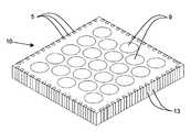
- the second, and the preferred approachis to generate an array of small, preferably round pads in a matching pattern on the semiconductor device and the underlying substrate.
- the diewill remain suitably aligned within the tube when the vacuum processes cause the braze material to melt, by virtue of the aligning force generated by the surface tension of the braze material.
- the described approachhas lead to better reproducibility in the positioning of semiconductor devices and better flatness than that achieved by prior techniques used in this field.
- the surface tension generated forcehas been shown to be sufficient to support the die, without significant position shift, in an inverted position while in a fully molten state.
- experiencehas shown that larger linear dimensions can be used with an indium braze as described than would be predicted by simple scaling of AuSn braze results. This may be explained by the fact that the indium remains ductile and thereby may relieve some of the residual strain induced by the TCE mismatch.
- the use of multiple small padscan also be used to address heat transfer issues between the die and underlying substrate. Although each individual braze may be small, the brazes can be tightly packed so as to cover a large fraction of the full die area thereby facilitating efficient heat transfer. This approach has been shown to be effective for die of about 1 cm square with no indication that this technique would not scale to larger die.
- Tube gapsare typically limited by the peak electric field present between the two biased planes of the tube, typically a photocathode or micro-channel plate (MCP) on the negative polarity side and the semiconductor device on the positive side.
- the design gapcan be estimated by adding the gap that creates the maximal design electric field to the height of any projections above the plane of the semiconductor device plus the parallelism tolerance of the package including that of the anode braze. For example, if one were to design for a maximum electric field of 200 V/mil and a 1000 V potential drop, the maximal electric field design gap would be 5 mils.
- Typical wire bondsextend above the plane of the anode by approximately 3 mils.
- Typical parallelism tolerances for fixtured brazesare ⁇ 2 mils.
- Multiple die bond padsare used to secure the semiconductor anode to the underlying substrate. In the preferred embodiment at least three distinct pads are used.
- the dieis secured via brazing.
- a low melting point, low vapor pressure, malleable materialis used for the braze. Indium and alloys thereof are good braze materials.
- Padsare typically deposited on the semiconductor device in a pattern that matches that of the intended substrate, typically a ceramic package. The following stack of materials has been demonstrated to generate a suitable braze pad:
- the SiO x N y layeracts as an insulator and a secondary barrier layer that is particularly useful when depositing on a silicon substrate.
- the chrome and platinum layersact as a barrier layer for the braze material.
- the final gold layeracts as a wetting agent for indium based brazes. This allows organic-free, flux free brazing to be performed with high yield. It should be noted that excessively thick gold layers can interfere with the reliability of the bond.
- the binary phase diagramreveals that a brittle inter-metallic compound, presumably AuIn 2 , is formed between indium and gold when they are allowed to mix in a molten state during the described braze and then solidify. This phase appears as brittle, roughly cubic crystals, in a matrix of relatively pure malleable indium.
- brazeswill no longer be malleable and substrate failure may occur.
- the braze between the semiconductor device and the packageis typically designed to be roughly columnar. Consequently, the fraction of gold in the indium braze, assuming a fixed deposition thickness on both surfaces and equilibrium braze conditions, is roughly inversely proportional to both indium mass/unit-area and bond thickness.
- Optimal semiconductor die positioning performanceis obtained when the braze pad diameter is greater than or equal to the braze thickness. Currently, 10 mil or larger pads are used to achieve a 6 mil braze thickness.
- FIG. 1is a schematic illustration of a semiconductor device showing the location and distribution of bond pads on a bottom surface.
- FIG. 2is a schematic illustration of the mating pattern of bond pads within a ceramic vacuum tube body.
- FIG. 3is a schematic cross section of a malleable braze showing the semiconductor device and its package.
- FIG. 4is a schematic of a cross sectional view of a bonded die in a packaged vacuum tube.
- FIG. 1illustrates a semiconductor device 10 suitable for use in the invention.
- This deviceis envisioned to be but not limited to an imaging sensor such as an electron bombarded CCD (EBCCD) or an electron bombarded CMOS or electron bombarded active pixel sensor (EBAPS), or an electron sensitive ROIC.
- the semiconductor devicemay lie in a thin layer on the side opposite that shown in FIG. 1 .
- the semiconductor deviceis typically bonded to a support structure of silicon or glass. This facilitates backthinning of the semiconductor device as for example is explained in U.S. Pat. No. 4,687,922 or in pending application Ser. No. 10/795,040 for improved electron bombarded imaging of such devices.
- U.S. Pat. No. 6,020,646describes one method of making a UHV compatible integrated circuit die assembly. Items 5 and 9 both represent braze pads of different sizes. Braze pad 5 overlies interconnect trace 13 thereby electrically connecting a bond pad on the opposite side of the die with interconnect braze pad 5 . Braze pad 9 , is electrically isolated from interconnect traces 13 and interconnect braze pads 5 . In the case of a silicon substrate, the pads and interconnects are typically deposited over a SiO x N y layer, ⁇ 3000 Angstroms in thickness.
- the SiO x N y layers extentmay be limited to where the trace 13 overlies the silicon present on the front and side of the device.
- Electrical traces 13are typically comprised of a 500 Angstroms thick titanium layer followed by 20,000 Angstroms of aluminum, followed by 500 Angstroms of chrome.
- Bond pads 5 and 9are typically comprised of Chrome—2000 Angstroms and Gold—500 Angstroms.
- Semiconductor device 1is approximately one cm square.
- indiumis the preferred braze material.
- materials including tin, silver, aluminum and galliumare useful in conjunction with each other or in conjunction with indium to form low melting point, low vapor pressure malleable braze joints.
- Other materials common in braze or solder materialssuch as bismuth, cadmium and lead exhibit somewhat higher vapor pressures and consequentially should be used with great caution in UHV applications.
- Braze pad geometrycan be varied over a fairly wide latitude. Generally though, there are a few guidelines that have resulted in reliable bonds.
- indiumas the braze material and standard Kyocera pad metallizations
- a nominal braze thickness of 5-8 milsis targeted. This is a functionally useful range in that indium volume can be adjusted to compensate for package tolerances.
- the braze thicknesscan be used to shim the gaps to meet manufacturing gap targets thereby allowing package tolerances to be relaxed. This results in a less expensive package. It should be noted that both average gap and parallelism may be shimmed in this manner.
- the minimum braze pad sizeis therefore specified by the upper range of the targeted braze thickness.
- Interconnect pads 5are approximately 10 mils in diameter. In practice, a minimum pad size of 10 mils diameter has been used with the 5-8 mil target braze thickness. Mixed pad sizes have been used on individual die without any apparent problems. Generally, pad arrays have been symmetrical so as to attempt to balance the TCE induced strain evenly amongst the pads.
- the pads, 9are electrically isolated, they primarily serve in a physical and heat transfer role. The pads, 9 , are typically larger than the electrical interconnect pads 5 .
- An array of pads, 9sized in the 50 to 100 mil range appear to work well to locate and transfer heat away from the semiconductor die assembly 10 .
- the targeted braze thickness of >5 milshas an additional vacuum processing benefit.
- the larger the gap between the base of the semiconductor die and the packagefacilitates more effective pumping of these surfaces during the vacuum bake cycle required in UHV tube processing.
- Electrical connection to the braze padsis made via a separate metal trace 13 .
- This traceis deposited between the SiO x N y layer and the first pad metal layer.
- Electrical tracesare typically comprised of a 500 Angstrom thick titanium layer followed by 20,000 Angstroms of aluminum, followed by 500 Angstroms of chrome.
- the electrical tracesare typically routed from the bond pad, around the sides of the die to the back bonding surface.
- indiumis used as the braze material, no wetting of the braze material to the traces is observed, no additional masking layer is required.
- this same metallization depositioncan be used within a generic ceramic package to redistribute the physical locations of bond pads so as to reflect the bond pad layout of a specific die. Referring now to FIG.
- the preferred shape of the die bond and interconnect padsis round, though non-round pads have been successfully used.
- the die bond pads 25are packed fairly densely in order to efficiently transfer heat from the semiconductor device to the package's back wall.
- the outline traced by interconnect pads 21is approximately 1 cm square, roughly matching the semiconductor die size.
- the semiconductor die 10is assembled with package 17 by placing braze material between each of the mating pads and running the physically stacked parts through a braze cycle.
- braze materialWhen indium is used as the braze material, the assembly will stick together when the parts are physically aligned and pressed together. No additional alignment or fixturing is required. Once a few of the sights bond, the surface tension of the braze material will both align in X and Y directions and pull the parts together in the Z dimension.
- an indium preformis positioned over metallized pad 27 . This causes the indium to melt and wet to pad 27 . This indium layer will subsequently be used to seal the vacuum tube to the photocathode.
- FIG. 3represents an un-scaled schematic cross section of the bonded die including an interconnect braze.
- semiconductor device 10is brazed to package 17 via a malleable braze 29 .
- the volume of braze materialis chosen in order to achieve a braze thickness of at least 4 mils.
- Layer 33represents the SiO x N y layer, which is typically approximately 3000 Angstroms thick and serves to electrically isolate interconnect traces.
- SiO x N ywas chosen because it is easy to deposit with a minimum of pinholes, a minimum of stress and it is easily etched from regions that need to be accessed.
- Layer 37represents that portion of the semiconductor device that contains active circuitry and interconnects.
- the sensorAfter the sensor has been run through the braze process, it is subjected to a vacuum bake-out and sealed to an activated photocathode 41 .
- the sealis accomplished by pressing photocathode 41 into the indium layer 45 that was previously wet to surface 27 .
- the proximity of photocathode 41 to semiconductor device 1illustrates the benefit of this approach over one that requires wire bonds off the top surface of 10 .
- the advantage of being able to shim the gap between 10 and 41 by measuring package depth and adjusting the volume of braze material used in braze 29becomes apparent.
- FIG. 4is a cross-sectional view of a semiconductor die assembly, 10 , attached via a low melting temperature braze material, 29 , to the surface of a ceramic package 17 .
- the brazeis formed between package pad 21 and semiconductor die assembly electrical interconnect pad 5 .
- Electrical interconnect pad 5is connected to the semiconductor circuit indicated by layer 37 via trace 13 . Electrical isolation of pad 5 and trace 13 is assured via SiO x N y layer 33 .
- FIG. 4is not drawn to scale, the thin films are expanded for clarity.
Landscapes
- Engineering & Computer Science (AREA)
- Computer Hardware Design (AREA)
- Microelectronics & Electronic Packaging (AREA)
- Power Engineering (AREA)
- Solid State Image Pick-Up Elements (AREA)
- Wire Bonding (AREA)
Abstract
Description
- The present invention is directed to the efficient and physically compliant attachment and interconnect of semiconductor die or semiconductor die assemblies in ultra high vacuum tubes.
- The present invention teaches a vacuum-compatible die bonding technique suitable for mounting die within a vacuum housing for use in a ultra high vacuum (UHV) tube. An application where this invention is particularly valuable is when used with charge coupled devices (CCDs) or CMOS in a vacuum environment in which the semiconductor die (CCD or CMOS) is directly electron bombarded in an imaging system as, for example, as is disclosed in U.S. Pat. No. 4,687,922 (CCDs) or as disclosed in U.S. Pat. No. 6,285,018 B1 (CMOS). This invention is also applicable for attaching hybrid read out integrated circuit devices (ROIC) to thermally mismatched substrates such as ceramics within photocathode based vacuum tubes.
- In the prior art, as described for example in U.S. Pat. 6,281,572, an intermediate pedestal is used between mismatched materials. The pedestal makes use of both an intermediate thermal coefficient of expansion (TCE) and a restricted area in order to limit the TCE mismatch induced strain in the finished device. The induced strain in the finished device is roughly proportional to the TCE mismatch times the change in temperature from the point at which the braze material solidified times the linear dimension of the braze. In the prior art, a braze material was chosen that remained in it's solid form throughout the tube vacuum process cycle. Typical braze materials and melting temperatures included AuSn (˜280° C.) and AuGe (˜361° C.) alloys. Modern photocathode based sensors including semiconductor devices are typically sealed under ultra-high vacuum (UHV) conditions. In order to achieve these conditions, tube components are typically baked at temperatures in excess of 200° C. in vacuum to eliminate residual gasses from tube components. Typically, the brazes are aligned using fixtures in order to accurately set the position of the semiconductor device within the tube. The fixtures are later removed and the tube is run through a UHV seal cycle. The high temperature of the braze alloys is required in the prior art to insure that the semiconductor does not move during the vacuum sealing step. The downside of the high temperature braze is that it locks in a high degree of strain in the finished assembly when it is cooled to room temperature. Another approach used in the prior art is to simply minimize the maximum linear dimension of the braze pad in order to minimize strain. A 0.050″ braze pad has been shown to work reasonably well with an AuSn braze. U.S. Pat. No. 6,507,147 describes a prior art package suitable for UHV applications that makes use of a small area braze. There is however a downside to this approach too. The use of a small pad limits the heat transfer area between the semiconductor device and the underlying substrate. In the case of electron bombarded CMOS image sensors or ROIC based CMOS anodes, heating of the sensor resulting from dissipation in the chip can and generally will result in degraded sensor performance. These difficulties in the prior art are avoided and/or considerably reduced through the use of physically compliant vacuum-compatible die bonding techniques enabling the efficient mounting of die within the vacuum area in a UHV tube.
- In prior art UHV tubes such as the one described in U.S. Pat. No. 6,281,572, electrical connection between the semiconductor device and the inside of the vacuum envelope has been made through the use of wire-bonds that extend from the exposed surface of the semiconductor die to the underlying surface of the vacuum package. The use of wire-bonds is a well-established, reliable way to make multiple electrical connections between a semiconductor device and a thermal coefficient of expansion mismatched package. The down side of this approach is the additional package volume dedicated to the annular ring of pads that lie outside the projected outline of the overlying semiconductor die. Through the use of low melting point physically compliant braze materials, the connection pads can be moved below the semiconductor die, thereby conserving package volume and projected area.
- The present invention minimizes or does away with the drawbacks of the prior art and in those instances in which a pedestal would have been used, eliminates this costly element. The present invention makes use of indium (melting point ˜156° C.) or other low melting point (less than about 200° C.) metals or alloys of metals, that remain ductile over the anticipated useful temperature range, to bond the semiconductor device to the underlying substrate. The choice of a low melting point bonding material means that the material will re-melt during vacuum processing of the tube. Pads are typically used as an intermediate between the semiconductor device or other substrate and the braze material, in order to specify the braze geometry and control the metallurgy of the braze. The re-melt issue is addressed in one of two ways. The first approach is to use a small centrally located pad (˜0.050″ max. linear dimension) on which a conventional braze material is used surrounded by a pad or pads on which a low melting point braze material is used. The second, and the preferred approach, is to generate an array of small, preferably round pads in a matching pattern on the semiconductor device and the underlying substrate. Through a suitable choice of pad, metallurgy, geometry, number, and braze material volume, the die will remain suitably aligned within the tube when the vacuum processes cause the braze material to melt, by virtue of the aligning force generated by the surface tension of the braze material. In fact, the described approach has lead to better reproducibility in the positioning of semiconductor devices and better flatness than that achieved by prior techniques used in this field. The surface tension generated force has been shown to be sufficient to support the die, without significant position shift, in an inverted position while in a fully molten state. Furthermore, experience has shown that larger linear dimensions can be used with an indium braze as described than would be predicted by simple scaling of AuSn braze results. This may be explained by the fact that the indium remains ductile and thereby may relieve some of the residual strain induced by the TCE mismatch. The use of multiple small pads can also be used to address heat transfer issues between the die and underlying substrate. Although each individual braze may be small, the brazes can be tightly packed so as to cover a large fraction of the full die area thereby facilitating efficient heat transfer. This approach has been shown to be effective for die of about 1 cm square with no indication that this technique would not scale to larger die.
- Electrical connections to semiconductor devices can also be achieved through the use of suitable metallurgy. The technique accommodates significant thermal coefficient of expansion mismatch and has been demonstrated to be reliable through multiple thermal cycles between room temperature and that of atmospheric pressure liquid nitrogen. The technique has the further major benefit for proximity-focused tubes that, unlike wire bonding, the new contacting scheme is effectively planar on the exposed surface. This allows the overlying tube wall to be moved closer to the semiconductor device surface without excessive yield losses. This in turn results in higher performance image sensors. This is particularly true for proximity focused vacuum image sensors where the semiconductor device is a CCD or CMOS imager. In this case, cathode-semiconductor gap or MCP-semiconductor gap directly affects imager resolution and a performance parameter called “Halo”. Tube gaps are typically limited by the peak electric field present between the two biased planes of the tube, typically a photocathode or micro-channel plate (MCP) on the negative polarity side and the semiconductor device on the positive side. The design gap can be estimated by adding the gap that creates the maximal design electric field to the height of any projections above the plane of the semiconductor device plus the parallelism tolerance of the package including that of the anode braze. For example, if one were to design for a maximum electric field of 200 V/mil and a 1000 V potential drop, the maximal electric field design gap would be 5 mils. Typical wire bonds extend above the plane of the anode by approximately 3 mils. Typical parallelism tolerances for fixtured brazes are ˜2 mils. Consequently, a ˜10 mil design gap is required in order to achieve a high production yield. Now if we take the case of semiconductor die bonded down as taught by this invention, the maximal field remains the same so we start with a 5 mil gap. Protrusion above the plane of the anode is <<1 mil. Parallelism tolerances have been demonstrated to be <0.5 mils. Consequently, the design gap for high yield production drops to ˜5.5. mils. This is a first order change that results in greatly improved resolution and Halo. Thus the present invention contributes to higher performance proximity focused tubes with the likelihood of improved resolution for such tubes.
- Similar electrical interconnect approaches have been investigated by the integrated circuit industry for use with flip-chip packaging and ball grid arrays (BGAs); however, the techniques developed for use with BGAs make use of organic materials. U.S. Pat. No. 6,656,768 describes a BGA packing approach. Organics make their way into the process in a number of ways: as a solder paste binder, as a soldering flux and finally as an under-fill material to enhance the mechanical and thermal performance of the finished device. However, organics cannot be used in a UHV processing environment since the photocathode of the vacuum tube for which this invention is intended suffers as a result of the use of organics in these roles. Organics have a tendency to break down and out-gas at the elevated temperatures required for UHV processing. Consequently, the elimination of the need to use organic compounds in these roles is another advantage of this invention.
- It is a further goal of this invention to be able to employ commercially available ceramic packages that are designed using standard processes and design rules. This includes making use of standard multi-layer ceramic packages as, for example, are described in Kyocera's “Multilayer Ceramics Design Guidelines”, 1995 CAT/2T9504THA/1244E. Other techniques for the manufacture of ceramic packages exist and may be used in this invention.
- Multiple die bond pads are used to secure the semiconductor anode to the underlying substrate. In the preferred embodiment at least three distinct pads are used. The die is secured via brazing. A low melting point, low vapor pressure, malleable material is used for the braze. Indium and alloys thereof are good braze materials. Pads are typically deposited on the semiconductor device in a pattern that matches that of the intended substrate, typically a ceramic package. The following stack of materials has been demonstrated to generate a suitable braze pad:
- SiOxNy—3000 Angstroms (The thickness and x/y ratio of this layer are not critical)
- Chrome—2000 Angstroms
- Gold—500 Angstroms
- An alternate stack of materials has also been demonstrated to generate a suitable braze pad:
- SiOxNy—3000 Angstroms (The thickness and x/y ratio of this layer are not critical)
- Titanium—200 Angstroms
- Platinum—5000 Angstroms
- Gold—500 Angstroms
- The SiOxNylayer acts as an insulator and a secondary barrier layer that is particularly useful when depositing on a silicon substrate. The chrome and platinum layers act as a barrier layer for the braze material. The final gold layer acts as a wetting agent for indium based brazes. This allows organic-free, flux free brazing to be performed with high yield. It should be noted that excessively thick gold layers can interfere with the reliability of the bond. The binary phase diagram reveals that a brittle inter-metallic compound, presumably AuIn2, is formed between indium and gold when they are allowed to mix in a molten state during the described braze and then solidify. This phase appears as brittle, roughly cubic crystals, in a matrix of relatively pure malleable indium. If the crystal fraction exceeds a critical value, the brazes will no longer be malleable and substrate failure may occur. Gold enters the braze from both the semiconductor braze pads and the package die bond pads. The braze between the semiconductor device and the package is typically designed to be roughly columnar. Consequently, the fraction of gold in the indium braze, assuming a fixed deposition thickness on both surfaces and equilibrium braze conditions, is roughly inversely proportional to both indium mass/unit-area and bond thickness. In practice using standard gold coated Kyocera die bond pads and the described semiconductor bond pads, braze thicknesses below 4 mils have proven to be unreliable, while brazes >=6 mils thick have proven to be quite robust. Optimal semiconductor die positioning performance is obtained when the braze pad diameter is greater than or equal to the braze thickness. Currently, 10 mil or larger pads are used to achieve a 6 mil braze thickness.
FIG. 1 is a schematic illustration of a semiconductor device showing the location and distribution of bond pads on a bottom surface.FIG. 2 is a schematic illustration of the mating pattern of bond pads within a ceramic vacuum tube body.FIG. 3 is a schematic cross section of a malleable braze showing the semiconductor device and its package.FIG. 4 is a schematic of a cross sectional view of a bonded die in a packaged vacuum tube.FIG. 1 illustrates asemiconductor device 10 suitable for use in the invention. This device is envisioned to be but not limited to an imaging sensor such as an electron bombarded CCD (EBCCD) or an electron bombarded CMOS or electron bombarded active pixel sensor (EBAPS), or an electron sensitive ROIC. In the case of the EBCCD and EBAPS devices, the semiconductor device may lie in a thin layer on the side opposite that shown inFIG. 1 . In these devices, the semiconductor device is typically bonded to a support structure of silicon or glass. This facilitates backthinning of the semiconductor device as for example is explained in U.S. Pat. No. 4,687,922 or in pending application Ser. No. 10/795,040 for improved electron bombarded imaging of such devices. In these cases,10 represents this bonded structure or semiconductor device. U.S. Pat. No. 6,020,646 describes one method of making a UHV compatible integrated circuit die assembly.Items Braze pad 5 overliesinterconnect trace 13 thereby electrically connecting a bond pad on the opposite side of the die withinterconnect braze pad 5.Braze pad 9, is electrically isolated from interconnect traces13 andinterconnect braze pads 5. In the case of a silicon substrate, the pads and interconnects are typically deposited over a SiOxNylayer, ˜3000 Angstroms in thickness. In the case of an EBCCD or EBAPS device mounted on Pyrex, the SiOxNylayers extent may be limited to where thetrace 13 overlies the silicon present on the front and side of the device. Electrical traces13 are typically comprised of a 500 Angstroms thick titanium layer followed by 20,000 Angstroms of aluminum, followed by 500 Angstroms of chrome.Bond pads - Pure indium is the preferred braze material. However, materials including tin, silver, aluminum and gallium are useful in conjunction with each other or in conjunction with indium to form low melting point, low vapor pressure malleable braze joints. Other materials common in braze or solder materials such as bismuth, cadmium and lead exhibit somewhat higher vapor pressures and consequentially should be used with great caution in UHV applications.
- Braze pad geometry can be varied over a fairly wide latitude. Generally though, there are a few guidelines that have resulted in reliable bonds. First, minimum pad size should be >=the braze thickness. When using indium as the braze material and standard Kyocera pad metallizations, a nominal braze thickness of 5-8 mils is targeted. This is a functionally useful range in that indium volume can be adjusted to compensate for package tolerances. In other words, the braze thickness can be used to shim the gaps to meet manufacturing gap targets thereby allowing package tolerances to be relaxed. This results in a less expensive package. It should be noted that both average gap and parallelism may be shimmed in this manner. The minimum braze pad size is therefore specified by the upper range of the targeted braze thickness.
Interconnect pads 5 are approximately 10 mils in diameter. In practice, a minimum pad size of 10 mils diameter has been used with the 5-8 mil target braze thickness. Mixed pad sizes have been used on individual die without any apparent problems. Generally, pad arrays have been symmetrical so as to attempt to balance the TCE induced strain evenly amongst the pads. The pads,9, are electrically isolated, they primarily serve in a physical and heat transfer role. The pads,9, are typically larger than theelectrical interconnect pads 5. An array of pads,9, sized in the 50 to 100 mil range appear to work well to locate and transfer heat away from the semiconductor dieassembly 10. - The targeted braze thickness of >5 mils has an additional vacuum processing benefit. The larger the gap between the base of the semiconductor die and the package facilitates more effective pumping of these surfaces during the vacuum bake cycle required in UHV tube processing.
- Electrical connection to the braze pads is made via a
separate metal trace 13. This trace is deposited between the SiOxNylayer and the first pad metal layer. Electrical traces are typically comprised of a 500 Angstrom thick titanium layer followed by 20,000 Angstroms of aluminum, followed by 500 Angstroms of chrome. The electrical traces are typically routed from the bond pad, around the sides of the die to the back bonding surface. When indium is used as the braze material, no wetting of the braze material to the traces is observed, no additional masking layer is required. Alternatively, this same metallization deposition can be used within a generic ceramic package to redistribute the physical locations of bond pads so as to reflect the bond pad layout of a specific die. Referring now toFIG. 2 the tube body of the preferred embodiment,17, is described, in great detail in U.S. Pat. No. 6,507,147. This patent does not describe the die and interconnect approach disclosed herein. Although a unitary ceramic body represents the preferred approach, the die and interconnect technique herein described is compatible with more traditional metal/ceramic brazed ultra high vacuum tube assemblies such as described in Publication US 2003/0066951 A1 for an intensified hybrid solid-state sensor.Interconnect pads 21 and diebond pads 25 are generated per standard multilayer ceramic package manufacturing methods as described in Kyocera's “Multilayer Ceramics Design Guidelines”, 1995 CAT/2T9504THA/1244E and similar design guides from other multilayer ceramic supplies. Diebond pads 25 are typically electrically connected together internally and brought out on a single pin from the opposite side of the package.Interconnect pads 21 are individually routed to separate pins on the opposite side of thepackage 27 designates a metallized pad. - The preferred shape of the die bond and interconnect pads is round, though non-round pads have been successfully used. The
die bond pads 25 are packed fairly densely in order to efficiently transfer heat from the semiconductor device to the package's back wall. InFIG. 2 , the outline traced byinterconnect pads 21 is approximately 1 cm square, roughly matching the semiconductor die size. - The semiconductor die10 is assembled with
package 17 by placing braze material between each of the mating pads and running the physically stacked parts through a braze cycle. When indium is used as the braze material, the assembly will stick together when the parts are physically aligned and pressed together. No additional alignment or fixturing is required. Once a few of the sights bond, the surface tension of the braze material will both align in X and Y directions and pull the parts together in the Z dimension. - During the braze process an indium preform is positioned over metallized
pad 27. This causes the indium to melt and wet to pad27. This indium layer will subsequently be used to seal the vacuum tube to the photocathode. FIG. 3 represents an un-scaled schematic cross section of the bonded die including an interconnect braze. In this Figure,semiconductor device 10 is brazed to package17 via amalleable braze 29. When using the metallization recipes listed forpad 5 and a Kyocera standard interconnect pad metallization for pad21 (seeFIG. 2 ), the volume of braze material is chosen in order to achieve a braze thickness of at least 4 mils. Layer33 (seeFIG. 4 ) represents the SiOxNylayer, which is typically approximately 3000 Angstroms thick and serves to electrically isolate interconnect traces. Almost any insulator can be used for this purpose, SiOxNywas chosen because it is easy to deposit with a minimum of pinholes, a minimum of stress and it is easily etched from regions that need to be accessed.Layer 37 represents that portion of the semiconductor device that contains active circuitry and interconnects.- After the sensor has been run through the braze process, it is subjected to a vacuum bake-out and sealed to an activated
photocathode 41. The seal is accomplished by pressingphotocathode 41 into theindium layer 45 that was previously wet to surface27. The proximity ofphotocathode 41 to semiconductor device1 illustrates the benefit of this approach over one that requires wire bonds off the top surface of10. Similarly, with standard flatness tolerances onpackage 17 on the order of 3 mils, the advantage of being able to shim the gap between10 and41 by measuring package depth and adjusting the volume of braze material used inbraze 29 becomes apparent. FIG. 4 is a cross-sectional view of a semiconductor die assembly,10, attached via a low melting temperature braze material,29, to the surface of aceramic package 17. The braze is formed betweenpackage pad 21 and semiconductor die assemblyelectrical interconnect pad 5.Electrical interconnect pad 5 is connected to the semiconductor circuit indicated bylayer 37 viatrace 13. Electrical isolation ofpad 5 and trace13 is assured via SiOxNylayer33.FIG. 4 is not drawn to scale, the thin films are expanded for clarity.- While there has been shown and discussed what are presently considered a preferred embodiment, it will be obvious to those skilled in the art that various changes and modifications may be made without departing from the scope of this invention and the coverage of the appended claims.
Claims (36)
Priority Applications (1)
| Application Number | Priority Date | Filing Date | Title |
|---|---|---|---|
| US11/324,074US7608533B2 (en) | 2004-05-14 | 2006-01-03 | Semiconductor die attachment for high vacuum tubes |
Applications Claiming Priority (2)
| Application Number | Priority Date | Filing Date | Title |
|---|---|---|---|
| US10/846,060US7012328B2 (en) | 2004-05-14 | 2004-05-14 | Semiconductor die attachment for high vacuum tubes |
| US11/324,074US7608533B2 (en) | 2004-05-14 | 2006-01-03 | Semiconductor die attachment for high vacuum tubes |
Related Parent Applications (1)
| Application Number | Title | Priority Date | Filing Date |
|---|---|---|---|
| US10/846,060DivisionUS7012328B2 (en) | 2004-05-14 | 2004-05-14 | Semiconductor die attachment for high vacuum tubes |
Publications (2)
| Publication Number | Publication Date |
|---|---|
| US20060113655A1true US20060113655A1 (en) | 2006-06-01 |
| US7608533B2 US7608533B2 (en) | 2009-10-27 |
Family
ID=35308623
Family Applications (2)
| Application Number | Title | Priority Date | Filing Date |
|---|---|---|---|
| US10/846,060Expired - LifetimeUS7012328B2 (en) | 2004-05-14 | 2004-05-14 | Semiconductor die attachment for high vacuum tubes |
| US11/324,074Active2025-12-31US7608533B2 (en) | 2004-05-14 | 2006-01-03 | Semiconductor die attachment for high vacuum tubes |
Family Applications Before (1)
| Application Number | Title | Priority Date | Filing Date |
|---|---|---|---|
| US10/846,060Expired - LifetimeUS7012328B2 (en) | 2004-05-14 | 2004-05-14 | Semiconductor die attachment for high vacuum tubes |
Country Status (4)
| Country | Link |
|---|---|
| US (2) | US7012328B2 (en) |
| EP (2) | EP3089208B1 (en) |
| JP (1) | JP5539618B2 (en) |
| WO (1) | WO2005114727A2 (en) |
Cited By (2)
| Publication number | Priority date | Publication date | Assignee | Title |
|---|---|---|---|---|
| US20050258212A1 (en)* | 2004-05-14 | 2005-11-24 | Intevac, Inc. | Semiconductor die attachment for high vacuum tubes |
| US7608533B2 (en) | 2004-05-14 | 2009-10-27 | Intevac, Inc. | Semiconductor die attachment for high vacuum tubes |
Families Citing this family (30)
| Publication number | Priority date | Publication date | Assignee | Title |
|---|---|---|---|---|
| US8816369B2 (en) | 2004-10-29 | 2014-08-26 | Led Engin, Inc. | LED packages with mushroom shaped lenses and methods of manufacturing LED light-emitting devices |
| US8324641B2 (en)* | 2007-06-29 | 2012-12-04 | Ledengin, Inc. | Matrix material including an embedded dispersion of beads for a light-emitting device |
| US9929326B2 (en) | 2004-10-29 | 2018-03-27 | Ledengin, Inc. | LED package having mushroom-shaped lens with volume diffuser |
| US8134292B2 (en)* | 2004-10-29 | 2012-03-13 | Ledengin, Inc. | Light emitting device with a thermal insulating and refractive index matching material |
| US7670872B2 (en)* | 2004-10-29 | 2010-03-02 | LED Engin, Inc. (Cayman) | Method of manufacturing ceramic LED packages |
| US7772609B2 (en)* | 2004-10-29 | 2010-08-10 | Ledengin, Inc. (Cayman) | LED package with structure and materials for high heat dissipation |
| US8283756B2 (en)* | 2007-08-20 | 2012-10-09 | Infineon Technologies Ag | Electronic component with buffer layer |
| US7972885B1 (en)* | 2008-09-25 | 2011-07-05 | Banpil Photonics, Inc. | Broadband imaging device and manufacturing thereof |
| US8075165B2 (en)* | 2008-10-14 | 2011-12-13 | Ledengin, Inc. | Total internal reflection lens and mechanical retention and locating device |
| US20100117106A1 (en)* | 2008-11-07 | 2010-05-13 | Ledengin, Inc. | Led with light-conversion layer |
| US8507300B2 (en)* | 2008-12-24 | 2013-08-13 | Ledengin, Inc. | Light-emitting diode with light-conversion layer |
| US8598793B2 (en) | 2011-05-12 | 2013-12-03 | Ledengin, Inc. | Tuning of emitter with multiple LEDs to a single color bin |
| US7985000B2 (en)* | 2009-04-08 | 2011-07-26 | Ledengin, Inc. | Lighting apparatus having multiple light-emitting diodes with individual light-conversion layers |
| CN101894901B (en) | 2009-04-08 | 2013-11-20 | 硅谷光擎 | Package for multiple light emitting diodes |
| US8303141B2 (en)* | 2009-12-17 | 2012-11-06 | Ledengin, Inc. | Total internal reflection lens with integrated lamp cover |
| US9345095B2 (en) | 2010-04-08 | 2016-05-17 | Ledengin, Inc. | Tunable multi-LED emitter module |
| US9080729B2 (en) | 2010-04-08 | 2015-07-14 | Ledengin, Inc. | Multiple-LED emitter for A-19 lamps |
| US8858022B2 (en) | 2011-05-05 | 2014-10-14 | Ledengin, Inc. | Spot TIR lens system for small high-power emitter |
| US8513900B2 (en) | 2011-05-12 | 2013-08-20 | Ledengin, Inc. | Apparatus for tuning of emitter with multiple LEDs to a single color bin |
| US11032884B2 (en) | 2012-03-02 | 2021-06-08 | Ledengin, Inc. | Method for making tunable multi-led emitter module |
| US9897284B2 (en) | 2012-03-28 | 2018-02-20 | Ledengin, Inc. | LED-based MR16 replacement lamp |
| US9234801B2 (en) | 2013-03-15 | 2016-01-12 | Ledengin, Inc. | Manufacturing method for LED emitter with high color consistency |
| US9406654B2 (en) | 2014-01-27 | 2016-08-02 | Ledengin, Inc. | Package for high-power LED devices |
| CN107004677B (en) | 2014-11-26 | 2020-08-25 | 硅谷光擎 | Compact transmitter for warm dimming and color-tunable lamps |
| US9530943B2 (en) | 2015-02-27 | 2016-12-27 | Ledengin, Inc. | LED emitter packages with high CRI |
| US10219345B2 (en) | 2016-11-10 | 2019-02-26 | Ledengin, Inc. | Tunable LED emitter with continuous spectrum |
| US10575374B2 (en) | 2018-03-09 | 2020-02-25 | Ledengin, Inc. | Package for flip-chip LEDs with close spacing of LED chips |
| CN112872720A (en)* | 2021-01-07 | 2021-06-01 | 南京精准传感科技有限公司 | Manufacturing process of brazed sensor sintering base |
| US11428531B1 (en) | 2021-03-22 | 2022-08-30 | Northrop Grumman Systems Corporation | Diffusion block for an evacuated instrument system |
| JP7610666B1 (en)* | 2023-09-07 | 2025-01-08 | 浜松ホトニクス株式会社 | Photodetector |
Citations (23)
| Publication number | Priority date | Publication date | Assignee | Title |
|---|---|---|---|---|
| US4437077A (en)* | 1980-08-08 | 1984-03-13 | Thomson-Csf | Semiconductor device usable at very high frequencies and its production process |
| US4687922A (en)* | 1984-11-30 | 1987-08-18 | U.S. Philips Corporation | Image detector operable in day or night modes |
| US5090609A (en)* | 1989-04-28 | 1992-02-25 | Hitachi, Ltd. | Method of bonding metals, and method and apparatus for producing semiconductor integrated circuit device using said method of bonding metals |
| US5760470A (en)* | 1995-02-10 | 1998-06-02 | Micron Display Technology, Inc. | Multi-layer electrical interconnection structures |
| US5800726A (en)* | 1995-07-26 | 1998-09-01 | International Business Machines Corporation | Selective chemical etching in microelectronics fabrication |
| US6020646A (en)* | 1997-12-05 | 2000-02-01 | The Charles Stark Draper Laboratory, Inc. | Intergrated circuit die assembly |
| US6194251B1 (en)* | 1997-12-18 | 2001-02-27 | Micron Technology, Inc. | Die positioning in integrated circuit packaging |
| US6238951B1 (en)* | 1993-05-28 | 2001-05-29 | Commissariat A L'energie Atomique | Process for producing a sealing and mechanical strength ring between a substrate and a chip hybridized by bumps on the substrate |
| US6281572B1 (en)* | 1997-12-05 | 2001-08-28 | The Charles Stark Draper Laboratory, Inc. | Integrated circuit header assembly |
| US6285018B1 (en)* | 1999-07-20 | 2001-09-04 | Intevac, Inc. | Electron bombarded active pixel sensor |
| US6507147B1 (en)* | 2000-08-31 | 2003-01-14 | Intevac, Inc. | Unitary vacuum tube incorporating high voltage isolation |
| US20030030149A1 (en)* | 2000-06-12 | 2003-02-13 | Kazuma Miura | Semiconductor device having solder bumps reliably reflow solderable |
| US6614110B1 (en)* | 1994-12-22 | 2003-09-02 | Benedict G Pace | Module with bumps for connection and support |
| US20030178476A1 (en)* | 2002-03-19 | 2003-09-25 | Kazuhisa Kanai | Solder paste, electronic -component assembly and soldering method |
| US20030186072A1 (en)* | 2000-06-12 | 2003-10-02 | Tasao Soga | Electron device and semiconductor device |
| US6656768B2 (en)* | 2001-02-08 | 2003-12-02 | Texas Instruments Incorporated | Flip-chip assembly of protected micromechanical devices |
| US6747258B2 (en)* | 2001-10-09 | 2004-06-08 | Itt Manufacturing Enterprises, Inc. | Intensified hybrid solid-state sensor with an insulating layer |
| US6764872B2 (en)* | 1999-12-27 | 2004-07-20 | Texas Instruments Incorporated | Microelectromechanical switch |
| US6847027B2 (en)* | 1999-03-18 | 2005-01-25 | Litton Systems, Inc. | Image intensifier tube |
| US7012328B2 (en)* | 2004-05-14 | 2006-03-14 | Intevac, Inc. | Semiconductor die attachment for high vacuum tubes |
| US7017795B2 (en)* | 2003-11-03 | 2006-03-28 | Indium Corporation Of America | Solder pastes for providing high elasticity, low rigidity solder joints |
| US20060220226A1 (en)* | 2005-03-30 | 2006-10-05 | Intel Corporation | Integrated heat spreader with intermetallic layer and method for making |
| US20070080451A1 (en)* | 2005-09-15 | 2007-04-12 | Intel Corporation | Intermetallic solder with low melting point |
Family Cites Families (15)
| Publication number | Priority date | Publication date | Assignee | Title |
|---|---|---|---|---|
| US4350886A (en)* | 1980-02-25 | 1982-09-21 | Rockwell International Corporation | Multi-element imager device |
| US4379218A (en)* | 1981-06-30 | 1983-04-05 | International Business Machines Corporation | Fluxless ion beam soldering process |
| US4921157A (en)* | 1989-03-15 | 1990-05-01 | Microelectronics Center Of North Carolina | Fluxless soldering process |
| JPH02303676A (en)* | 1989-05-17 | 1990-12-17 | Hitachi Ltd | Joining method by brazing material and treating device as well as semiconductor device |
| JPH06333987A (en)* | 1993-05-18 | 1994-12-02 | Hitachi Ltd | Electric circuit junction device and electric circuit junction method |
| US5370301A (en)* | 1994-01-04 | 1994-12-06 | Texas Instruments Incorporated | Apparatus and method for flip-chip bonding |
| JPH08139096A (en)* | 1994-11-07 | 1996-05-31 | Sony Corp | Electronic component, mounting of electronic component and electronic component mounting device |
| JPH09129680A (en)* | 1995-10-26 | 1997-05-16 | Hitachi Ltd | Semiconductor pellet and semiconductor device using the same |
| JPH1070153A (en)* | 1996-08-26 | 1998-03-10 | Hitachi Ltd | How to connect electronic components |
| CA2213034C (en)* | 1996-09-02 | 2002-12-17 | Murata Manufacturing Co., Ltd. | A semiconductor device with a passivation film |
| JP4098852B2 (en)* | 1997-07-24 | 2008-06-11 | 浜松ホトニクス株式会社 | Electron tube |
| US6303986B1 (en) | 1998-07-29 | 2001-10-16 | Silicon Light Machines | Method of and apparatus for sealing an hermetic lid to a semiconductor die |
| AU1983199A (en)* | 1999-01-21 | 2000-08-07 | Hamamatsu Photonics K.K. | Electron tube |
| JP2001053074A (en)* | 1999-08-05 | 2001-02-23 | Seiko Epson Corp | Semiconductor device and manufacturing method thereof |
| US6581640B1 (en)* | 2000-08-16 | 2003-06-24 | Kelsey-Hayes Company | Laminated manifold for microvalve |
- 2004
- 2004-05-14USUS10/846,060patent/US7012328B2/ennot_activeExpired - Lifetime
- 2005
- 2005-05-02WOPCT/US2005/015086patent/WO2005114727A2/ennot_activeApplication Discontinuation
- 2005-05-02JPJP2007513190Apatent/JP5539618B2/ennot_activeExpired - Fee Related
- 2005-05-02EPEP16171775.6Apatent/EP3089208B1/ennot_activeExpired - Lifetime
- 2005-05-02EPEP05742093.7Apatent/EP1745506B1/ennot_activeExpired - Lifetime
- 2006
- 2006-01-03USUS11/324,074patent/US7608533B2/enactiveActive
Patent Citations (24)
| Publication number | Priority date | Publication date | Assignee | Title |
|---|---|---|---|---|
| US4437077A (en)* | 1980-08-08 | 1984-03-13 | Thomson-Csf | Semiconductor device usable at very high frequencies and its production process |
| US4687922A (en)* | 1984-11-30 | 1987-08-18 | U.S. Philips Corporation | Image detector operable in day or night modes |
| US5090609A (en)* | 1989-04-28 | 1992-02-25 | Hitachi, Ltd. | Method of bonding metals, and method and apparatus for producing semiconductor integrated circuit device using said method of bonding metals |
| US6238951B1 (en)* | 1993-05-28 | 2001-05-29 | Commissariat A L'energie Atomique | Process for producing a sealing and mechanical strength ring between a substrate and a chip hybridized by bumps on the substrate |
| US6614110B1 (en)* | 1994-12-22 | 2003-09-02 | Benedict G Pace | Module with bumps for connection and support |
| US5760470A (en)* | 1995-02-10 | 1998-06-02 | Micron Display Technology, Inc. | Multi-layer electrical interconnection structures |
| US5800726A (en)* | 1995-07-26 | 1998-09-01 | International Business Machines Corporation | Selective chemical etching in microelectronics fabrication |
| US6020646A (en)* | 1997-12-05 | 2000-02-01 | The Charles Stark Draper Laboratory, Inc. | Intergrated circuit die assembly |
| US6281572B1 (en)* | 1997-12-05 | 2001-08-28 | The Charles Stark Draper Laboratory, Inc. | Integrated circuit header assembly |
| US6194251B1 (en)* | 1997-12-18 | 2001-02-27 | Micron Technology, Inc. | Die positioning in integrated circuit packaging |
| US6847027B2 (en)* | 1999-03-18 | 2005-01-25 | Litton Systems, Inc. | Image intensifier tube |
| US6285018B1 (en)* | 1999-07-20 | 2001-09-04 | Intevac, Inc. | Electron bombarded active pixel sensor |
| US6764872B2 (en)* | 1999-12-27 | 2004-07-20 | Texas Instruments Incorporated | Microelectromechanical switch |
| US20030030149A1 (en)* | 2000-06-12 | 2003-02-13 | Kazuma Miura | Semiconductor device having solder bumps reliably reflow solderable |
| US20030186072A1 (en)* | 2000-06-12 | 2003-10-02 | Tasao Soga | Electron device and semiconductor device |
| US6837766B2 (en)* | 2000-08-31 | 2005-01-04 | Intevac, Inc. | Unitary vacuum tube incorporating high voltage isolation |
| US6507147B1 (en)* | 2000-08-31 | 2003-01-14 | Intevac, Inc. | Unitary vacuum tube incorporating high voltage isolation |
| US6656768B2 (en)* | 2001-02-08 | 2003-12-02 | Texas Instruments Incorporated | Flip-chip assembly of protected micromechanical devices |
| US6747258B2 (en)* | 2001-10-09 | 2004-06-08 | Itt Manufacturing Enterprises, Inc. | Intensified hybrid solid-state sensor with an insulating layer |
| US20030178476A1 (en)* | 2002-03-19 | 2003-09-25 | Kazuhisa Kanai | Solder paste, electronic -component assembly and soldering method |
| US7017795B2 (en)* | 2003-11-03 | 2006-03-28 | Indium Corporation Of America | Solder pastes for providing high elasticity, low rigidity solder joints |
| US7012328B2 (en)* | 2004-05-14 | 2006-03-14 | Intevac, Inc. | Semiconductor die attachment for high vacuum tubes |
| US20060220226A1 (en)* | 2005-03-30 | 2006-10-05 | Intel Corporation | Integrated heat spreader with intermetallic layer and method for making |
| US20070080451A1 (en)* | 2005-09-15 | 2007-04-12 | Intel Corporation | Intermetallic solder with low melting point |
Cited By (4)
| Publication number | Priority date | Publication date | Assignee | Title |
|---|---|---|---|---|
| US20050258212A1 (en)* | 2004-05-14 | 2005-11-24 | Intevac, Inc. | Semiconductor die attachment for high vacuum tubes |
| US7608533B2 (en) | 2004-05-14 | 2009-10-27 | Intevac, Inc. | Semiconductor die attachment for high vacuum tubes |
| US7607560B2 (en) | 2004-05-14 | 2009-10-27 | Intevac, Inc. | Semiconductor die attachment for high vacuum tubes |
| WO2007015965A3 (en)* | 2005-07-28 | 2008-07-24 | Intevac Inc | Semiconductor die attachment for high vacuum tubes |
Also Published As
| Publication number | Publication date |
|---|---|
| JP5539618B2 (en) | 2014-07-02 |
| WO2005114727A2 (en) | 2005-12-01 |
| US20050253242A1 (en) | 2005-11-17 |
| EP1745506A2 (en) | 2007-01-24 |
| JP2007537598A (en) | 2007-12-20 |
| EP3089208A1 (en) | 2016-11-02 |
| US7608533B2 (en) | 2009-10-27 |
| US7012328B2 (en) | 2006-03-14 |
| WO2005114727A3 (en) | 2006-02-02 |
| EP1745506A4 (en) | 2008-09-17 |
| EP1745506B1 (en) | 2016-07-13 |
| EP3089208B1 (en) | 2018-01-24 |
Similar Documents
| Publication | Publication Date | Title |
|---|---|---|
| US7608533B2 (en) | Semiconductor die attachment for high vacuum tubes | |
| EP1907159B1 (en) | Semiconductor die attachment for high vacuum tubes | |
| US7750462B1 (en) | Microelectromechanical systems using thermocompression bonding | |
| US5185613A (en) | Hybrid structures | |
| US7429724B1 (en) | Low profile wire bond for an electron sensing device in an image intensifier tube | |
| US4168630A (en) | Semiconductor pressure converter | |
| US5273940A (en) | Multiple chip package with thinned semiconductor chips | |
| US6204090B1 (en) | Method for attaching a die to a carrier utilizing an electrically nonconductive layer | |
| JPH06244231A (en) | Airtight semiconductor device and manufacture thereof | |
| CN111403376B (en) | A kind of hermetic packaging structure of integrated thermoelectric refrigerator and preparation method thereof | |
| US20110253430A1 (en) | Micro pin hybrid interconnect array and method of manufacturing same | |
| US6281572B1 (en) | Integrated circuit header assembly | |
| JP2000100869A (en) | Semiconductor device and method of manufacturing the same | |
| US20060156737A1 (en) | Cooling structure of solid state and formation thereof with integrated package | |
| JP6445109B2 (en) | Photoelectric device package structure and method for packaging photoelectric chip | |
| JPH08107164A (en) | Semiconductor device | |
| Soucy et al. | An approach to MEM sensor array packaging | |
| JPS6197932A (en) | Crimp type semiconductor package | |
| JP2003209314A (en) | Package for storing optical semiconductor elements | |
| KR100359790B1 (en) | semiconductor package and manufacturing method the same | |
| JPH0513506A (en) | Semiconductor integrated circuit device | |
| JPS6334962A (en) | Structure for package | |
| JPH04207056A (en) | Manufacture of multi-chip module device and frame body with cap used for the same | |
| JPH03138966A (en) | Semiconductor integrated circuit device | |
| JP2001119059A (en) | Superconducting radioaction detecting device |
Legal Events
| Date | Code | Title | Description |
|---|---|---|---|
| AS | Assignment | Owner name:INTEVAC, INC., CALIFORNIA Free format text:ASSIGNMENT OF ASSIGNORS INTEREST;ASSIGNORS:COSTELLO, KENNETH A.;RODERICK, KEVIN JAMES;REEL/FRAME:019665/0080 Effective date:20070801 | |
| STCF | Information on status: patent grant | Free format text:PATENTED CASE | |
| REMI | Maintenance fee reminder mailed | ||
| FPAY | Fee payment | Year of fee payment:4 | |
| SULP | Surcharge for late payment | ||
| FPAY | Fee payment | Year of fee payment:8 | |
| FEPP | Fee payment procedure | Free format text:ENTITY STATUS SET TO SMALL (ORIGINAL EVENT CODE: SMAL); ENTITY STATUS OF PATENT OWNER: SMALL ENTITY | |
| MAFP | Maintenance fee payment | Free format text:PAYMENT OF MAINTENANCE FEE, 12TH YR, SMALL ENTITY (ORIGINAL EVENT CODE: M2553); ENTITY STATUS OF PATENT OWNER: SMALL ENTITY Year of fee payment:12 | |
| AS | Assignment | Owner name:BLUE TORCH FINANCE LLC, NEW YORK Free format text:PATENT SECURITY AGREEMENT;ASSIGNORS:EOTECH, LLC;HEL TECHNOLOGIES, LLC;REEL/FRAME:058600/0351 Effective date:20211230 | |
| AS | Assignment | Owner name:EOTECH, LLC, MICHIGAN Free format text:ASSIGNMENT OF ASSIGNORS INTEREST;ASSIGNOR:INTEVAC, INC;REEL/FRAME:058589/0494 Effective date:20211230 | |
| AS | Assignment | Owner name:BLUE TORCH FINANCE LLC, AS ADMINISTRATIVE AGENT, NEW YORK Free format text:PATENT SECURITY AGREEMENT;ASSIGNOR:EOTECH, LLC;REEL/FRAME:059725/0564 Effective date:20211230 | |
| AS | Assignment | Owner name:HEL TECHNOLOGIES, LLC, MICHIGAN Free format text:NOTICE OF RELEASE OF SECURITY INTEREST IN PATENT COLLATERAL;ASSIGNOR:BLUE TORCH FINANCE LLC, AS COLLATERAL AGENT;REEL/FRAME:064356/0155 Effective date:20230721 Owner name:EOTECH, LLC, MICHIGAN Free format text:NOTICE OF RELEASE OF SECURITY INTEREST IN PATENT COLLATERAL;ASSIGNOR:BLUE TORCH FINANCE LLC, AS COLLATERAL AGENT;REEL/FRAME:064356/0155 Effective date:20230721 | |
| AS | Assignment | Owner name:KEYBANK NATIONAL ASSOCIATION, AS ADMINISTRATIVE AGENT, OHIO Free format text:SECURITY INTEREST;ASSIGNOR:EOTECH, LLC;REEL/FRAME:064571/0724 Effective date:20230721 | |
| AS | Assignment | Owner name:PHOTONICS WEST, LLC, MICHIGAN Free format text:ASSIGNMENT OF ASSIGNORS INTEREST;ASSIGNOR:EOTECH, LLC;REEL/FRAME:068644/0238 Effective date:20240827 | |
| AS | Assignment | Owner name:PHOTONICS WEST, LLC, MICHIGAN Free format text:CORRECTIVE ASSIGNMENT TO CORRECT THE THE APPLICATION NUMBER INCORRECTLY LISTED AS PATENT NUMBER PREVIOUSLY RECORDED AT REEL: 68644 FRAME: 238. ASSIGNOR(S) HEREBY CONFIRMS THE ASSIGNMENT;ASSIGNOR:EOTECH, LLC;REEL/FRAME:069057/0092 Effective date:20240827 | |
| AS | Assignment | Owner name:KEYBANK NATIONAL ASSOCIATION, AS ADMINISTRATIVE AGENT, OHIO Free format text:SECURITY INTEREST;ASSIGNOR:PHOTONICS WEST, LLC;REEL/FRAME:069110/0610 Effective date:20241001 |