US20060110880A1 - Self-aligned trench filling with high coupling ratio - Google Patents
Self-aligned trench filling with high coupling ratioDownload PDFInfo
- Publication number
- US20060110880A1 US20060110880A1US10/996,030US99603004AUS2006110880A1US 20060110880 A1US20060110880 A1US 20060110880A1US 99603004 AUS99603004 AUS 99603004AUS 2006110880 A1US2006110880 A1US 2006110880A1
- Authority
- US
- United States
- Prior art keywords
- conductive layer
- layer
- trench
- nand string
- forming
- Prior art date
- Legal status (The legal status is an assumption and is not a legal conclusion. Google has not performed a legal analysis and makes no representation as to the accuracy of the status listed.)
- Granted
Links
Images


Classifications
- H—ELECTRICITY
- H10—SEMICONDUCTOR DEVICES; ELECTRIC SOLID-STATE DEVICES NOT OTHERWISE PROVIDED FOR
- H10B—ELECTRONIC MEMORY DEVICES
- H10B41/00—Electrically erasable-and-programmable ROM [EEPROM] devices comprising floating gates
- H10B41/30—Electrically erasable-and-programmable ROM [EEPROM] devices comprising floating gates characterised by the memory core region
- H—ELECTRICITY
- H01—ELECTRIC ELEMENTS
- H01L—SEMICONDUCTOR DEVICES NOT COVERED BY CLASS H10
- H01L21/00—Processes or apparatus adapted for the manufacture or treatment of semiconductor or solid state devices or of parts thereof
- H01L21/02—Manufacture or treatment of semiconductor devices or of parts thereof
- H01L21/04—Manufacture or treatment of semiconductor devices or of parts thereof the devices having potential barriers, e.g. a PN junction, depletion layer or carrier concentration layer
- H01L21/18—Manufacture or treatment of semiconductor devices or of parts thereof the devices having potential barriers, e.g. a PN junction, depletion layer or carrier concentration layer the devices having semiconductor bodies comprising elements of Group IV of the Periodic Table or AIIIBV compounds with or without impurities, e.g. doping materials
- H01L21/28—Manufacture of electrodes on semiconductor bodies using processes or apparatus not provided for in groups H01L21/20 - H01L21/268
- H01L21/28008—Making conductor-insulator-semiconductor electrodes
- H01L21/28017—Making conductor-insulator-semiconductor electrodes the insulator being formed after the semiconductor body, the semiconductor being silicon
- H01L21/28026—Making conductor-insulator-semiconductor electrodes the insulator being formed after the semiconductor body, the semiconductor being silicon characterised by the conductor
- H01L21/28123—Lithography-related aspects, e.g. sub-lithography lengths; Isolation-related aspects, e.g. to solve problems arising at the crossing with the side of the device isolation; Planarisation aspects
- H01L21/28141—Lithography-related aspects, e.g. sub-lithography lengths; Isolation-related aspects, e.g. to solve problems arising at the crossing with the side of the device isolation; Planarisation aspects insulating part of the electrode is defined by a sidewall spacer, e.g. dummy spacer, or a similar technique, e.g. oxidation under mask, plating
- H—ELECTRICITY
- H01—ELECTRIC ELEMENTS
- H01L—SEMICONDUCTOR DEVICES NOT COVERED BY CLASS H10
- H01L21/00—Processes or apparatus adapted for the manufacture or treatment of semiconductor or solid state devices or of parts thereof
- H01L21/70—Manufacture or treatment of devices consisting of a plurality of solid state components formed in or on a common substrate or of parts thereof; Manufacture of integrated circuit devices or of parts thereof
- H01L21/71—Manufacture of specific parts of devices defined in group H01L21/70
- H01L21/76—Making of isolation regions between components
- H01L21/762—Dielectric regions, e.g. EPIC dielectric isolation, LOCOS; Trench refilling techniques, SOI technology, use of channel stoppers
- H01L21/76224—Dielectric regions, e.g. EPIC dielectric isolation, LOCOS; Trench refilling techniques, SOI technology, use of channel stoppers using trench refilling with dielectric materials
- H—ELECTRICITY
- H01—ELECTRIC ELEMENTS
- H01L—SEMICONDUCTOR DEVICES NOT COVERED BY CLASS H10
- H01L21/00—Processes or apparatus adapted for the manufacture or treatment of semiconductor or solid state devices or of parts thereof
- H01L21/70—Manufacture or treatment of devices consisting of a plurality of solid state components formed in or on a common substrate or of parts thereof; Manufacture of integrated circuit devices or of parts thereof
- H01L21/71—Manufacture of specific parts of devices defined in group H01L21/70
- H01L21/768—Applying interconnections to be used for carrying current between separate components within a device comprising conductors and dielectrics
- H01L21/76838—Applying interconnections to be used for carrying current between separate components within a device comprising conductors and dielectrics characterised by the formation and the after-treatment of the conductors
- H—ELECTRICITY
- H10—SEMICONDUCTOR DEVICES; ELECTRIC SOLID-STATE DEVICES NOT OTHERWISE PROVIDED FOR
- H10B—ELECTRONIC MEMORY DEVICES
- H10B69/00—Erasable-and-programmable ROM [EPROM] devices not provided for in groups H10B41/00 - H10B63/00, e.g. ultraviolet erasable-and-programmable ROM [UVEPROM] devices
Definitions
- Embodiments of the present inventionare directed to high density semiconductor devices, such as nonvolatile memory, and systems and methods for isolating active regions and components in high density semiconductor devices.
- Integrated circuitsare constructed by electrically connecting multiple isolated devices that share a common substrate. When multiple devices are formed on or in a common substrate, it is necessary to isolate the individual devices using isolation technology. As the density of integrated circuits continues to increase, the space available for isolating devices tends to decrease. With decreased device dimensions, inter-device parasitic currents and charges can become more problematic, making isolation technology a critical component of integrated circuit fabrication.
- nonvolatile semiconductor memory devicessuch as flash memory
- many individual storage elementsare constructed from a common substrate to form a memory array. These individual storage elements must be isolated from one another using isolation technology.
- the NAND structureis used.
- the NAND structureincludes multiple transistors arranged in series, sandwiched between two select gates. The transistors in series and the select gates are referred to as a NAND string. Isolation technologies are typically employed during the device fabrication process to provide electrical isolation between adjacent NAND strings sharing a common substrate.
- LOCOSLocal Oxidation of Silicon
- an oxideis grown or deposited on the surface of a substrate, followed by the deposition of a nitride layer over the oxide layer. After patterning these layers to expose the desired isolation areas and cover the desired active areas, a trench is etched into these layers and a portion of the substrate. An oxide is then grown on the exposed regions. The grown oxide typically grows under the deposited nitride causing the encroachment of oxide into the active regions (often referred to as a bird's beak). This encroachment can cause stresses and ultimately defects in the silicon.
- LOCLocal Oxidation of Silicon
- the encroachmentdecreases the available active area for constructing devices which limits the density that can be achieved in the integrated circuit.
- the LOCOS techniquecan cause alignment issues since the trench is formed prior to forming layers such as the conductive layer used to fabricate the floating gate of a device. For example, the subsequently formed floating gate material may not properly align between two predefined trenches.
- SWAMIsidewall-masked isolation
- a nitrideis formed on the trench walls prior to forming the oxide to decrease the oxide's encroachment and formation of bird's beaks. While this process provides an improvement to conventional LOCOS, the nitride in the trench rises during oxidation, causing encroachment into the active areas. This technique also yields excessive stress in the corners of the trench since oxide growth in that region is restrained. Moreover, the trenches are formed prior to device fabrication leading to the aforementioned alignment issues.
- a deep, narrow trenchis etched into a substrate between active regions.
- the deep, narrow trenchcan form an effective isolation region between active regions without occupying as much lateral substrate area as required by other techniques such as shallow trench isolation.
- the trenchis filled by growing a suitable dielectric such as silicon dioxide.
- the dielectricgrows from the substrate to fill the trench and into the substrate to provide a dielectric of greater width and depth than the trench.
- Storage elements for a NAND type flash memory systemfor example, can be fabricated by etching the substrate to form the trench after or as part of etching to form NAND string active areas.
- This techniquestands in contrast to prior art techniques (e.g., LOCOS) where the trench is formed prior to device active areas such as a NAND string active area. This can ensure alignment of the NAND string active areas between isolation trenches. Because the dielectric growth process is self-limiting, an open area resulting from the etching process can be maintained between the stacks. A subsequently formed inter-gate dielectric layer and control gate layer can fill the open area to provide sidewall coupling between control gates and floating gates. In prior art techniques that employ deposition to fill trenches, the area between NAND string active areas is filled with the dielectric that is deposited for the trench such that the control gate only overlies the floating gate in a vertical direction. There can be no sidewall coupling in such prior art configurations.
- a method of fabricating a nonvolatile memory deviceincludes forming a first dielectric layer above a substrate and forming a first conductive layer above the first dielectric layer. After forming these layers, the method continues by etching through the first conductive layer, the first dielectric layer, and at least a portion of the substrate to define a trench in the substrate between a first portion of the first conductive layer and a second portion of the conductive layer. The trench is filled by growing a dielectric material. The method then continues by forming a second dielectric layer above the first conductive layer and forming a second conductive layer above the second dielectric layer.
- a nonvolatile memory devicein another embodiment, includes a substrate, a first dielectric layer formed above the substrate, a first conductive layer having a first portion that is subdivided to form floating gates for a first group of storage elements of the integrated circuit and a second portion that is subdivided to form floating gates for a second group of storage elements of the integrated circuit, and a trench etched in the substrate between the first portion and the second portion of the first conductive layer. The trench is filled with a grown dielectric.
- the circuitfurther includes a second dielectric layer formed above the first portion and the second portion of the first conductive layer, and a second conductive layer formed above the second dielectric layer.
- the second conductive layerforms control gates for the first group of storage elements and the second group of storage elements.
- the second layeris subdivided to form word lines of the integrated circuit.
- a method of fabricating a nonvolatile memoryincludes forming an isolation trench in a substrate between a first NAND string active area and a second NAND string active area.
- the first NAND string active area and second NAND string active areaeach include a first dielectric portion and a first conductive portion.
- the first dielectric portion and the first conductive portion of the first NAND string active area and the second NAND string active areaare formed prior to the isolation trench.
- the methodfurther includes filling the trench with a grown dielectric material to isolate the first NAND string active area from the second NAND string active area.
- FIG. 1is a top view of a NAND string.
- FIG. 2is an equivalent circuit diagram of the NAND string depicted in FIG. 1 .
- FIG. 3is a circuit diagram depicting three NAND strings.
- FIG. 4is a two-dimensional block diagram of one embodiment of a flash memory cell that can be fabricated in accordance with one embodiment.
- FIG. 5is a three dimensional drawing of a pair of four word line long portions of two NAND strings that can be fabricated in accordance with one embodiment.
- FIGS. 6A-6Hdepict NAND string stacks in accordance with one embodiment at various stages of a fabrication process in accordance with one embodiment.
- FIG. 7is flowchart of a method of fabricating flash memory cells in accordance with one embodiment.
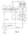
- FIG. 8is a block diagram of one example of a memory system that can be used to implement the present invention.
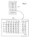
- FIG. 9illustrates an example of an organization of a memory array.
- FIG. 10is a flow chart describing one embodiment of a process for programming non-volatile memory devices.
- FIG. 11is a flow chart describing one embodiment of a process for reading non-volatile memory devices.
- FIG. 1is a top view showing one NAND string.
- FIG. 2is an equivalent circuit thereof.
- Trench isolation techniques in accordance with embodimentsare presented with respect to nonvolatile flash memory and NAND type memory for purposes of explanation. It will be appreciated by those of oridinary skill in the art, however, that the techniques set forth are not so limited and can be utilized in many fabrication processes to fabricate various types of integrated circuits.
- the NAND string depicted in FIGS. 1 and 2includes four transistors 100 , 102 , 104 and 106 in series and sandwiched between a first select gate 120 and a second select gate 122 .
- Select gate 120connects the NAND string to bit line 126 .
- Select gate 122connects the NAND string to source line 128 .
- Each of the transistors 100 , 102 , 104 and 106includes a control gate and a floating gate.
- transistor 100has control gate 100 CG and floating gate 100 FG.
- Transistor 102includes control gate 102 CG and a floating gate 102 FG.
- Transistor 104includes control gate 104 CG and floating gate 104 FG.
- Transistor 106includes a control gate 106 CG and a floating gate 106 FG.
- Control gate 100 CGis connected to word line WL 3
- control gate 102 CGis connected to word line WL 2
- control gate 104 CGis connected to word line WL 1
- control gate 106 CGis connected to word line WL 0 .
- FIGS. 1 and 2show four memory cells in the NAND string, the use of four transistors is only provided as an example.
- a NAND stringcan have less than four memory cells or more than four memory cells.
- some NAND stringswill include eight memory cells, 16 memory cells, 32 memory cells, etc.
- FIG. 3shows three NAND strings 202 , 204 and 206 of a memory array having many more NAND strings.
- Each of the NAND strings of FIG. 3includes two select transistors and four memory cells.
- Each stringis connected to the source line by its select transistor (e.g. select transistor 230 and select transistor 250 ).
- a selection line SGSis used to control the source side select gates.
- the various NAND stringsare connected to respective bit lines by select transistors 220 , 240 , etc., which are controlled by select line SGD.
- Each word line(WL 3 , WL 2 , WL 1 and WL 0 ) is connected to the control gate of one memory cell on each NAND string forming a row of cells.
- word line WL 2is connected to the control gates for memory cell 224 , 244 , and 252 .
- each bit line and the respective NAND stringcomprise the columns of the array of memory cells. In NAND structures, it is necessary to isolate the individual NAND strings and associated storage elements from one another using isolation technology.
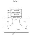
- FIG. 4is a two-dimensional block diagram of one embodiment of a flash memory cell such as those depicted in FIGS. 1-3 that can be fabricated in accordance with embodiments.
- the memory cell of FIG. 4includes a triple well comprising a P-substrate, an N-well, and a P-well. The P-substrate and the N-well are not depicted in FIG. 4 in order to simplify the drawing.
- Within P-well 320are N+ doped regions 324 , which serve as source/drain regions for the memory cell. Whether N+ doped regions 324 are labeled as source regions or drain regions is somewhat arbitrary. Therefore, the N+ doped source/drain regions 324 can be thought of as source regions, drain regions, or both.
- a channel 322Between N+ doped regions 324 is a channel 322 .
- a first dielectric area or layer 330Above channel 322 is a first dielectric area or layer 330 .
- dielectric layer 330Above dielectric layer 330 is a conductive area or layer 332 that forms a floating gate of the memory cell.
- the floating gateunder low-voltage operating conditions associated with read or bypass operations, is electrically insulated/isolated from channel 322 by the first dielectric layer 330 .
- Above floating gate 332is a second dielectric area or layer 334 .
- Above dielectric layer 334Above dielectric layer 334 is a second conductive layer 336 that forms a control gate of the memory cell.
- various layersmay be interspersed within or added to the illustrated layers. For example, additional layers can be placed above control gate 336 , such as a hard mask.
- dielectric 330 , floating gate 332 , dielectric 332 , and control gate 336comprise a stack. An array of memory cells
- EEPROMelectrically erasable programmable read-only memory
- a program voltageis typically applied to the control gate and the bit line is grounded. Electrons from the channel are injected into the floating gate as electrons tunnel across dielectric 330 . Dielectric 330 is often referred to as a tunnel dielectric or tunnel oxide.
- the program voltage applied to the control gateis applied as a series of pulses. The magnitude of the pulses is increased with each successive pulse by a pre-determined step size.
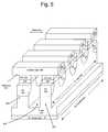
- FIG. 5is a three-dimensional block diagram of two typical NAND strings 302 and 304 that may be fabricated as part of a larger flash memory array.
- FIG. 5depicts four memory cells on strings 302 and 304 . However, more or less than four memory cells can be used.
- Each of the memory cells of the NAND stringhas a stack as described above with respect to FIG. 4 .
- N-well 326below P-well 320 , the bit line direction along the NAND string, and the word line direction perpendicular to the NAND string.
- the P-type substrate below N-well 336is not shown in FIG. 5 .
- the control gatesform the word lines.
- a continuous layer of conductive layer 336is formed which is consistent across a word line in order to provide a common word line or control gate for each device on that word line.
- NAND string 302When fabricating a NAND-based non-volatile memory system, including NAND strings as depicted in FIG. 5 , it is necessary to provide electrical isolation between adjacent strings.
- NAND string 302must be electrically isolated from NAND string 304 in order to provide discreet devices with independent electrical characteristics. Isolation of the memory cells on NAND string 302 from the memory cells on NAND string 304 is typically accomplished by providing an electrical barrier between the strings in order to inhibit or prevent parasitic currents and charges between adjacent memory cells.
- NAND string 302is separated from NAND string 304 by an open area or void 306 .
- a dielectric materialis formed between adjacent NAND strings and would be present at the position of open area 306 .
- many prior art techniquesinclude forming a dielectric isolation region prior to forming the stacks for each memory cell using a LOCOS process, for example.
- the ability to provide electrical isolationis often measured in terms of a field threshold.
- the field thresholdrepresents the amount of charge or current that a particular isolation technique can withstand.
- an isolation regionmay provide a 10 volt field threshold such that it can withstand a charge of 10 volts placed across it.
- the charge levels within the circuitare continuing to increase.
- the influence of a floating gate over the channel regioncan decrease.
- high program voltagesare applied to the control gates. For example, in many non-volatile flash memory devices, a program voltage of 20 volts or more can be applied.
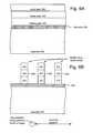
- FIGS. 6A through 6Hdepict a sequential process for forming isolation regions between active areas in an integrated circuit in accordance with one embodiment.
- FIG. 7is a flow chart depicting a process for forming isolation regions during the fabrication of non-volatile memory devices such as that depicted in FIGS. 6A-6H .
- FIGS. 6A-6H and FIG. 7depict a specific example with respect to a NAND flash memory device.
- FIGS. 6A-6Hdepict a specific example with respect to a NAND flash memory device.
- the bit line direction, relative to the pageruns in and out of the page while the word line direction runs left to right relative to the page.
- FIG. 6Adepicts a substrate 300 on and in which multiple non-volatile NAND-type flash memory devices are to be fabricated.
- Substrate 300is used generically to represent a substrate, but can also include P-wells and/or N-wells formed therein, as appropriate for various implementations.
- a P-well and N-wellmay be formed in substrate 300 as depicted in FIGS. 4 and 5 .
- Dielectric 330can form the tunnel oxide of storage elements.
- Dielectric layer 330can include an oxide or other suitable dielectric material in various embodiments.
- Dielectric layer 330can be deposited using known chemical vapor deposition (CVD) processes, metal organic CVD processes, physical vapor deposition (PVD) processes, atomic layer deposition (ALD) processes, grown using a thermal oxidation process, or formed using another suitable process.
- CVDchemical vapor deposition
- PVDphysical vapor deposition
- ALDatomic layer deposition
- dielectric 330is about 70-100 angstroms in thickness. However, thicker or thinner layers can be used in accordance with various embodiments. Additionally (and optionally), other materials may be deposited on, deposited under, or incorporated within the dielectric to form dielectric layer 330 .
- a first conductive layer 332(e.g., polysilicon) is deposited on top of the tunnel oxide layer.
- First conductive layer 332will comprise the floating gates for the memory devices of the strings being fabricated.
- conductive layer 332is polysilicon deposited using known processes as described above. In other embodiments, other conductive materials can be used.
- conductive layer 332is about 500 angstroms in thickness. However, conductive layers thicker or thinner than 500 angstroms can be used in accordance with embodiments.
- a nitride layer 340is deposited at step 408 and an oxide layer 342 deposited at step 410 .
- These oxide and nitride layersserve as sacrificial layers for various later-performed steps.
- Both the oxide and nitride layerscan be formed using known processes, and each layer can be about 400 angstroms in thickness. However the thickness of each of these layers can be more or less than 400 angstroms in accordance with various embodiments.
- Layers 330 , 332 , 340 , and 342are preliminary NAND string active area layers that are used to form a plurality of devices. Multiple NAND strings will be constructed using these layers as starting layers.
- a hard maskcan be deposited (step 412 ) over oxide layer 342 to begin the process of defining the individual NAND strings of the device.
- photolithographycan be used to form strips of photoresist over the areas to become the NAND strings.
- the exposed mask layerscan be etched using anisotropic plasma etching, for example.
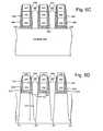
- the oxide layer, nitride layer, and floating gate layerare etched using the photoresist and mask to form the individual NAND string active areas 380 , 382 , and 384 .
- the result of such a processis depicted in FIG. 6B .
- FIG. 6Bdepicts floating gate layer 332 , nitride layer 340 , and oxide layer 342 , after etching to form three distinct preliminary NAND string active areas that will become individual NAND strings for the memory device.
- the three NAND string active areasare adjacent to one another in the word line direction.
- a layer of oxideis deposited on the exposed surfaces (step 416 ) to begin formation of sidewall spacers for each defined string. After depositing the oxide, it is etched back from substrate 300 to form first sidewall spacer layers 344 for each NAND string. Dielectric 330 is also etched to expose those areas of substrate 300 outside the spacer and in between the preliminary active areas.
- FIG. 6Cdepicts oxide spacer layers 344 after having been deposited and etched.
- FIG. 6Cfurther illustrates the stacks after deposition and etching to form nitride spacer layers 346 .
- layers 344 and 346form a sidewall spacer on each sidewall of each NAND string stack.
- the sidewall spacersserve as a mask for the trench etching steps to follow in order to narrow the width of the trenches that will be formed between adjacent NAND strings in the memory device.
- the sidewall spacer on NAND string active area 380 and the adjacent sidewall spacer on NAND string active area 382will be used to define a trench between active areas 380 and 382 .
- a narrow deep trenchis etched (step 420 ) into substrate 300 to begin the formation of isolation regions between adjacent NAND strings.
- FIG. 6Ddepicts the substrate after etching to form trenches 350 .
- Trenches 350are etched between adjacent NAND string active areas. The trench has slanted walls which become narrower towards the bottom of the trench. Because of the formation of sidewall spacers (layers 344 and 346 ) prior to etching, the width of the trench can be narrow in comparison to trenches formed using prior art techniques.
- trenches 230are about 2,000 angstroms deep and about 300 angstroms in width at the top.
- oxide layer 342serves as a sacrificial layer for the etching process.
- the thickness of oxide layer 342is decreased during the etching process.
- narrow trenchescan enable decreases in overall device dimension sizes by facilitating closer spacing of NAND strings. Because a very deep trench is used, a high field threshold can be obtained, while still maintaining a narrow trench width.
- the amount of field threshold accomplished by an isolation region using a trench, as depicted in FIGS. 6A through 6His dependant upon the aspect ratio defined by the width/height ratio of the trench.
- a deep, narrow trenchis used in order to decrease device dimension size, while also maintaining a suitable aspect ratio.
- a high field thresholdcan be maintained while decreasing device dimensions.
- sidewall spacerslayers 344 and 346 ) enables a narrow trench to be formed, while also serving as a mask, as previously described.
- the oxide and nitride layerswill serve to constrict the etching to between the adjacent nitride spacer layers.
- the top of the trenchwill be narrower than the space between adjacent NAND-strings by an amount equal to twice the width of each oxide spacer layer and each nitride spacer layer.
- floating gate layer 332 prior to etching trenches 350avoids mis-alignment issues that may exist in prior art techniques that form an isolation region prior to forming a floating gate layer. Because the floating gate layer is formed first and etched along with the substrate to form a trench, the trench will be properly aligned between the floating gates of memory cells on adjacent NAND strings. In prior art techniques where the trench is formed first, care must be taken to properly form the floating gate layer between predefined isolation regions. The imprecision of growth and deposition processes may cause the floating gate to not be properly positioned between the isolation regions. Such is not the case in accordance with embodiments herein because the floating gate is accurately positioned in between the trenches due to etching after forming the floating gate.
- the trenchesare filled by thermally growing (and/or depositing) an oxide or other suitable dielectric material (e.g., nitride) from the bottom and sides of the trench to substantially fill the trench with a grown oxide (step 422 ).
- the trenchcan be filled using known thermal growth techniques for growing oxides from a silicon substrate. For example, exposing the silicon substrate to an oxygen containing mixture will cause oxidation of the silicon, and the formation of silicon-dioxide within the trench. The silicon-dioxide will grow from both the bottom of the trench and each of the sidewalls of the trench. This growth process is self-limiting.
- step 422can include a combination of chemical vapor deposition and oxide growth. For example, a small thin layer of oxide can be deposited along the sidewalls and bottom of the trench in order to form a cushion between the silicon substrate and subsequently grown oxide. After forming this thin layer along the walls and bottom of the trench, an oxide can be grown to completely fill the trench as previously described.
- FIG. 6Eillustrates the result of thermally growing oxide 352 in trenches 350 .
- Oxide 352has filled each of trenches 350 and extends beyond the top of the trench, to about the level of the bottom of the first conductive layer 330 .
- the resulting width and depth of the silicon dioxideis wider and deeper than the originally etched trenches 350 .
- the resulting width and depthis due to the silicon dioxide not only growing from the sidewalls and the bottom of the trench into the trench, but also from the silicon dioxide growing from the sidewalls and the bottom of the trench into substrate 300 itself. As illustrated, this results in an oxide that is wider and deeper than the initial trench etched into the substrate.
- the width of oxide at the top of each trenchextends to encompass substantially all of the space between adjacent NAND string active areas.
- the effective oxide width at the top of the trenchcan reach about 600 angstroms after growing an oxide.
- the 2000 angstrom depth of the trenchcan be extended by oxide growth to about 2200 angstroms.
- Step 424exposes the tops and sides of the floating gate layers of each NAND string active area, as depicted in FIG. 6F .
- a second dielectric layeris formed above and in between the etched portions of floating gate layer 332 at step 426 .
- the second dielectric layerforms the inter-gate dielectric for the individual storage devices of each string.
- the second dielectric layeris formed of multiple individual layers of dielectric material. As depicted in FIG.
- the dielectric layercan be formed of a first layer of oxide 362 , a second layer of nitride 360 , and a third layer of oxide 364 (oxide layer 364 is depicted on the outside of nitride layer 364 , but without any substantial thickness shown in the figure.)
- a dielectric comprised of oxygen/nitrogen/oxygen layersis often referred to as an ONO dielectric.
- the total depth of the second dielectric layercan be about 290 angstroms.
- oxide layer 362can be about 120 angstroms
- nitride layer 360about 120 angstroms
- the second oxide layer 364about 50 angstroms.
- the second dielectric layercan be greater or less than 290 angstroms and the individual layers can be greater than or less than the specified dimensions and be formed of alternate materials.
- the dielectric layeris formed by depositing each of the oxide and nitride layers using processes such as chemical vapor deposition. The dielectric layer can be densified using known densification techniques. The combination of a 120 angstrom oxide, a 120 angstrom nitride, and a 50 angstrom oxide layer has an effective ONO thickness of about 140 angstroms.
- a second conductive layer 370is deposited over the exposed regions of the structure at step 428 .
- conductive layer 370is poly-silicon and forms the control gates for multiple non-volatile memory cells.
- poly-silicon layer 370is deposited to a depth of about 2000 angstroms from the top of the second dielectric layer. As illustrated in FIG. 6H , poly-silicon layer 370 is not only deposited above dielectric layer 370 , but also in between adjacent NAND string active areas to fill the areas 366 between the floating gates of each NAND string. For example, poly-silicon layer 370 will fill the area between NAND string active area 380 and NAND string active area 382 .
- the control gate layerwill surround the floating gate layer (and be separated from the control gate layer by the second dielectric layer) on three sides—the top and both sidewalls of the floating gate.
- the resulting coupling force from the control gate to the floating gatewill include three coupling components.
- a first componentresults from coupling between a bottom portion of the control gate layer and the top portion of floating gate layer.
- a second and third componentresult from coupling between sidewall portions of the control gate layer and the two sidewalls of the floating gate of the stack.
- the floating gateswill be aligned between two trenches as previously described.
- the second dielectric layeris self-aligned over each floating gate and thus provides consistent coupling at each formed cell. Since etching occurs through the floating gate layer and into the substrate to form the trench, consistent spacing and alignment of floating gates is achieved. Accordingly, the control gate layer will be consistently formed around each floating gate which leads to consistent coupling characteristics for each device. In prior art techniques where the floating gate layers are mis-aligned, the subsequently formed control gate layer may not be consistenly formed around each floating gate. This can lead to different coupling characteristics between cells.
- a gap 366exists between each of the NAND string active areas after formation of the second dielectric layer.
- the oxidewill not only be deposited into the trench, but will also be deposited over any other exposed layers.
- the oxidewill not only fill the trench as depicted in FIGS. 6E and 6F , but will also extend above the top of the trench and over each of the floating gate layers 332 .
- the oxidewill fill the gap areas such as areas 366 depicted in FIG. 6G .
- CMPchemical mechanical polishing
- Chemical mechanical polishing processesare not capable of selectively etching between the stacks. Accordingly, the top of the oxide will be commensurate and level with the top of the floating gate layer 332 . Accordingly, no gap is able to be created between the NAND strings, as depicted in FIG. 6G .
- the subsequent deposition of a second dielectric layere.g., layers 360 , 362 , and 364 ), will only deposit such a dielectric layer on top of the floating gate layers.
- the subsequently deposited control gate layerwill only extend above the floating gates, and not in between the floating gates, as depicted in FIG. 6H . Since the influence of a control gate over a respective floating gate is governed by the opposing surface areas of each of the layers, this limits the achievable coupling ratio.
- the coupling forces from the control gate to the floating gatewill only extend in one direction—from the bottom of the control gate layer to the top of the floating gate layer.
- the coupling ratio in such scenariosis only proportional to the bottom surface area of the control gate and top surface area of the floating gate. The coupling ratio will not be effected by or benefit from the thickness (top to bottom relative to paper) of the floating gate layer.
- the poly-silicon layeris deposited both above the floating gate layer, as well as in between adjacent portions of the floating gate layer.
- the control of the control gate over the floating gateis governed by the top surface area of the top of the floating gate due to top to bottom coupling and also by the thickness of poly-silicon layer 370 due to sidewall coupling.
- the coupling achieved in prior art techniques where the control gate only overlies the floating gate in a vertical directionis equal to some constant multiplied by ⁇ .
- the couplingis enhanced by sidewall coupling.
- the sidewall couplingis also equal to the same constant multiplied by the thickness T. Since there will be coupling from two sides, the total sidewall coupling is equal to the constant multiplied by 2T. Since the overall coupling is equal to the sidewall and top coupling values, the overall coupling ratio is equal to the constant multiplied by ⁇ +2T, rather than just ⁇ as in prior art techniques.
- control gate layer 370After depositing control gate layer 370 , the active areas can be subdivided to form word lines that are isolated from one another.
- a mask layercan be deposited on control gate layer 370 and photolithography used to form strips of photoresist perpendicular to the NAND string (formed in the word line direction).
- the exposed portions of the mask and underlying layerscan be etched using plasma etching, ion milling, ion etching that is purely physical etching, or another suitable process to etch the various layers and form the individual word lines by subdividing the control gate layer, the inter-gate dielectric layer, and the floating gate layers.
- the etched portions of the control gate layerform the individual word lines. In one embodiment, etching is performed until the tunnel dielectric layer is reached. In another embodiment, etching continues through the tunnel dielectric until the substrate is reached.
- FIG. 8is a block diagram of one embodiment of a flash memory system that can be used to implement the present invention.
- Memory cell array 502is controlled by column control circuit 504 , row control circuit 506 , c-source control circuit 510 and p-well control circuit 508 .
- Array 502can include one or more memory cells fabricated according to embodiments set forth in FIGS. 6 and 7 .
- Column control circuit 504is connected to the bit lines of memory cell array 502 for reading data stored in the memory cells, for determining a state of the memory cells during a program operation, and for controlling potential levels of the bit lines to promote or inhibit programming and erasing.
- Row control circuit 506is connected to the word lines to select one of the word lines, to apply read voltages, to apply program voltages combined with the bit line potential levels controlled by column control circuit 504 , and to apply an erase voltage.
- C-source control circuit 510controls a common source line (labeled as “C-source” in FIG. 6 ) connected to the memory cells.
- P-well control circuit 508controls the p-well voltage.
- the data stored in the memory cellsare read out by the column control circuit 504 and are output to external I/O lines via data input/output buffer 512 .
- Program data to be stored in the memory cellsare input to the data input/output buffer 512 via the external I/O lines, and transferred to the column control circuit 504 .
- the external I/O linesare connected to controller 518 .
- Command data for controlling the flash memory deviceare input to controller 518 .
- the command datainforms the flash memory of what operation is requested.
- the input commandis transferred to state machine 516 that controls column control circuit 504 , row control circuit 506 , c-source control 510 , p-well control circuit 508 and data input/output buffer 512 .
- State machine 516can also output status data of the flash memory such as READY/BUSY or PASS/FAIL.
- Controller 518is connected to or connectable with a host system such as a personal computer, a digital camera, or personal digital assistant, etc. It communicates with the host that initiates commands, such as to store or read data to or from the memory array 502 , and provides or receives such data. Controller 518 converts such commands into command signals that can be interpreted and executed by command circuits 514 , which is in communication with state machine 516 . Controller 518 typically contains buffer memory for the user data being written to or read from the memory array.
- One exemplary memory systemcomprises one integrated circuit that includes controller 518 , and one or more integrated circuit chips that each contain a memory array and associated control, input/output and state machine circuits.
- the memory systemmay be embedded as part of the host system, or may be included in a memory card (or other package) that is removably inserted into the host systems.
- a memory cardmay include the entire memory system (e.g. including the controller) or just the memory array(s) with associated peripheral circuits (with the controller or control function being embedded in the host).
- the controllercan be embedded in the host or included within the removable memory system.
- FIG. 9an exemplary structure of memory cell array 502 is described.
- a NAND flash EEPROMis described that is partitioned into 1,024 blocks.
- the data stored in each blockcan be simultaneously erased.
- the blockis the minimum unit of cells that are simultaneously erased.
- the bit linesare also divided into even bit lines (BLe) and odd bit lines (BLo).
- FIG. 9shows four memory cells connected in series to form a NAND string. Although four cells are shown to be included in each NAND string, more or less than four can be used (e.g., 16, 32, or another number).
- One terminal of the NAND stringis connected to a corresponding bit line via a first select transistor (also referred to as a select gate) SGD, and another terminal is connected to c-source via a second select transistor SGS.
- a first select transistoralso referred to as a select gate
- 4,256 memory cellsare simultaneously selected.
- the memory cells selectedhave the same word line (e.g. WL2-i), and the same kind of bit line (e.g. even bit lines). Therefore, 532 bytes of data can be read or programmed simultaneously. These 532 bytes of data that are simultaneously read or programmed form a logical page. Therefore, in this example, one block can store at least eight pages. When each memory cell stores two bits of data (e.g. a multi-level cell), one block stores 16 pages.
- the select gates (SGD and SGS) of a selected blockare raised to one or more select voltages and the unselected word lines (e.g., WL 0 , WL 1 and WL 3 ) of the selected block are raised to a read pass voltage (e.g. 4.5 volts) to make the transistors operate as pass gates.
- the selected word line of the selected blocke.g., WL 2
- a reference voltagea level of which is specified for each read and verify operation in order to determine whether a threshold voltage of the concerned memory cell is above or below such level.
- the selected word line WL 2is grounded, so that it is detected whether the threshold voltage is higher than 0V.
- the selected word line WL 2is connected to 2.4V, for example, so that as programming progresses it is verified whether or not the threshold voltage has reached 2.4V.
- the source and p-wellare at zero volts during read and verify.
- the selected bit lines (BLe)are pre-charged to a level of, for example, 0.7V. If the threshold voltage is higher than the read or verify level, the potential level of the concerned bit line (BLe) maintains the high level, because of the associated non-conductive memory cell.
- the threshold voltageis lower than the read or verify level, the potential level of the concerned bit line (BLe) decreases to a low level, for example less than 0.5V, because of the conductive memory cell.
- the state of the memory cellis detected by a sense amplifier that is connected to the bit line and senses the resulting bit line voltage.
- the difference between whether the memory cell is programmed or eraseddepends on whether or not net negative charge is stored in the floating gate. For example, if negative charge is stored in the floating gate, the threshold voltage becomes higher and the transistor can be in enhancement mode of operation.
- the drain and the p-wellreceive 0 volts while the control gate receives a series of programming pulses with increasing magnitudes.
- the magnitudes of the pulses in the seriesrange from 7 volts to 20 volts. In other embodiments, the range of pulses in the series can be different, for example, having a starting level of higher than 7 volts.
- verify operationsare carried out in the periods between the programming pulses. That is, the programming level of each cell of a group of cells being programmed in parallel is read between each programming pulse to determine whether or not it has reached or exceeded a verify level to which it is being programmed.
- One means of verifying the programmingis to test conduction at a specific compare point.
- the cells that are verified to be sufficiently programmedare locked out, for example in NAND cells, by raising the bit line voltage from 0 to Vdd (e.g., 2.5 volts) for all subsequent programming pulses to terminate the programming process for those cells.
- Vdde.g. 2.5 volts
- the number of pulseswill be limited (e.g. 20 pulses) and if a given memory cell is not sufficiently programmed by the last pulse, an error is assumed.
- memory cellsare erased (in blocks or other units) prior to programming.
- FIG. 10is a flowchart describing a method for programming a non-volatile memory system. As will be apparent to those of ordinary skill in the art, various steps can be modified, added, or removed depending on a specific application or implementation while still remaining within the scope and spirit of the present disclosure. In various implementations, memory cells are erased (in blocks or other units) prior to programming.
- a data load commandis issued by controller 518 and input to command circuit 514 , allowing data to be input to data input/output buffer 512 .
- the input datais recognized as a command and latched by state machine 516 via a command latch signal, not illustrated, input to command circuits 514 .
- step 652address data designating the page address is input to row controller 506 from controller 518 .
- the input datais recognized as the page address and latched via state machine 516 , effected by the address latch signal input to command circuits 514 .
- step 654532 bytes of program data are input to data input/output buffer 512 . It should be noted that 532 bytes of program data are specific to the particular implementation described, and other implementations will require or utilize various other sizes of program data. That data can be latched in a register for the selected bit lines. In some embodiments, the data is also latched in a second register for the selected bit lines to be used for verify operations.
- a program commandis issued by controller 318 and input to data input/output buffer 512 . The command is latched by state machine 316 via the command latch signal input to command circuits 514
- Vpgmthe programming pulse voltage level applied to the selected word line
- the starting pulsee.g. 12 volts
- a program counter PCmaintained by state machine 516
- Vpgma program voltage (Vpgm) pulse is applied to the selected word line.
- the bit lines that include a memory cell to be programmedare grounded to enable programming, while the other bit lines are connected to Vdd to inhibit programming during application of the programming pulse.
- the states of the selected memory cellsare verified. If it is detected that the target threshold voltage of a selected cell has reached the appropriate level (for example, the programmed level for logic 0 or a particular state of a multi-state cell), then the selected cell is verified as programmed to its target state. If it is detected that the threshold voltage has not reached the appropriate level, the selected cell is not verified as programmed to its target state. Those cells verified as programmed to their target state at step 362 will be excluded from further programming.
- it is determined whether all cells to be programmed have been verified to have programmed to their corresponding statessuch as by checking an appropriate data storage register designed to detect and signal such a status.
- the programming processis complete and successful because all selected memory cells were programmed and verified to their target states. A status of pass is reported in step 666 . If at step 664 , it is determined that not all of the memory cells have been so verified, then the programming process continues.
- the program counter PCis checked against a program limit value. One example of a program limit value is 20. If the program counter PC is not less than 20, then the program process is flagged as failed and a status of fail is reported at step 670 . If the program counter PC is less than 20, then the Vpgm level is increased by the step size and the program counter PC is incremented at step 672 . After step 672 , the process loops back to step 660 to apply the next Vpgm program pulse. At the end of a successful program process, the threshold voltages of the memory cells should be within one or more distributions of threshold voltages for programmed memory cells or within a distribution of threshold voltages for erased memory cells.
- the flowchart of FIG. 10depicts a single-pass programming method as can be applied for binary storage.
- a two-pass programming methodas can be applied for multi-level storage, for example, multiple programming or verification steps may be used in a single iteration of the flowchart.
- Steps 360 - 372may be performed for each pass of the programming operation.
- one or more program pulsesmay be applied and the results thereof verified to determine if a cell is in the appropriate intermediate state.
- one or more program pulsesmay be applied and the results thereof verified to determine if the cell is in the appropriate final state.
- FIG. 11is a flow chart describing one embodiment of a process for reading a memory cell in array 502 .
- a read commandis received from the host and stored in the state machine.
- an addressis received and stored.
- the process of FIG. 11assumes a four state memory cell, with an erased state and three programmed states. Therefore, in one embodiment, three read operations are performed in order to read the data stored in the memory cell. If the memory has eight states, then seven read operations are performed; if the memory has sixteen states, then fifteen read operations are performed, etc.
- the first read operationis performed.
- a first read compare pointequivalent to a threshold voltage between state 0 and state 1 is applied to the selected word line, and the sense amplifier on each bit line makes a binary decision as to whether the cell at the intersection of the selected word line and the corresponding bit line is on or off. If the cell is detected to be on, then it is read as being in state 0, otherwise the cell is in state 1, 2 or 3. In other words, if the threshold voltage of the memory cell is greater than the first read compare point, the memory cell is assumed to be in the erased state 0.
- step 708the second read operation is performed.
- a second read compare pointequivalent to a threshold voltage between state 2 and state 1 is applied to the selected word line, and the sense amplifier on each bit line makes a binary decision as to whether the cell at the intersection of the selected word line and the corresponding bit line is on or off.
- An “off” bit lineindicate that the corresponding memory cell is either in state 0 or in state 1.
- An “on” bit lineindicates that the corresponding memory cell is in either state 2 or state 3.
- step 710the third read operation is performed.
- a third read compare pointequivalent to a threshold voltage between state 3 and state 2 is applied to the selected word line, and the sense amplifier on each bit line makes a binary decision as to whether the cell at the intersection of the selected word line and the corresponding bit line is on or off.
- An “off” bit linewill indicate that the corresponding cell is either in state 0, in state 1, or in state 2.
- An “on” bit linewill indicate that the corresponding memory cell is in state 3.
- the information obtained during the three sequential steps explained aboveis stored in latches.
- a decoderis used to combine the results of the three read operations in order to find the state of each cell.
- state 1would be a result of the following three read results: on in step 706 , off in step 708 , and off in step 710 .
- the above sequence of the read operationscan be reversed, corresponding to the verify waveform sequence depicted in FIG. 5 . Note that other read processes can also be used with the present invention.
Landscapes
- Engineering & Computer Science (AREA)
- Physics & Mathematics (AREA)
- Condensed Matter Physics & Semiconductors (AREA)
- General Physics & Mathematics (AREA)
- Manufacturing & Machinery (AREA)
- Computer Hardware Design (AREA)
- Microelectronics & Electronic Packaging (AREA)
- Power Engineering (AREA)
- Semiconductor Memories (AREA)
- Non-Volatile Memory (AREA)
Abstract
Description
- 1. Field of the Invention
- Embodiments of the present invention are directed to high density semiconductor devices, such as nonvolatile memory, and systems and methods for isolating active regions and components in high density semiconductor devices.
- 2. Description of the Related Art
- Integrated circuits are constructed by electrically connecting multiple isolated devices that share a common substrate. When multiple devices are formed on or in a common substrate, it is necessary to isolate the individual devices using isolation technology. As the density of integrated circuits continues to increase, the space available for isolating devices tends to decrease. With decreased device dimensions, inter-device parasitic currents and charges can become more problematic, making isolation technology a critical component of integrated circuit fabrication.
- For example, in nonvolatile semiconductor memory devices such as flash memory, many individual storage elements are constructed from a common substrate to form a memory array. These individual storage elements must be isolated from one another using isolation technology. In one example of a flash memory system, the NAND structure is used. The NAND structure includes multiple transistors arranged in series, sandwiched between two select gates. The transistors in series and the select gates are referred to as a NAND string. Isolation technologies are typically employed during the device fabrication process to provide electrical isolation between adjacent NAND strings sharing a common substrate.
- Numerous techniques exist for isolating devices in NAND flash memory and other types of semiconductor devices. In Local Oxidation of Silicon (LOCOS) techniques, an oxide is grown or deposited on the surface of a substrate, followed by the deposition of a nitride layer over the oxide layer. After patterning these layers to expose the desired isolation areas and cover the desired active areas, a trench is etched into these layers and a portion of the substrate. An oxide is then grown on the exposed regions. The grown oxide typically grows under the deposited nitride causing the encroachment of oxide into the active regions (often referred to as a bird's beak). This encroachment can cause stresses and ultimately defects in the silicon. Furthermore, the encroachment decreases the available active area for constructing devices which limits the density that can be achieved in the integrated circuit. Additionally, the LOCOS technique can cause alignment issues since the trench is formed prior to forming layers such as the conductive layer used to fabricate the floating gate of a device. For example, the subsequently formed floating gate material may not properly align between two predefined trenches.
- Improvements to these processes have been made by employing such techniques as sidewall-masked isolation (SWAMI) to decrease encroachment into active areas. In SWAMI, a nitride is formed on the trench walls prior to forming the oxide to decrease the oxide's encroachment and formation of bird's beaks. While this process provides an improvement to conventional LOCOS, the nitride in the trench rises during oxidation, causing encroachment into the active areas. This technique also yields excessive stress in the corners of the trench since oxide growth in that region is restrained. Moreover, the trenches are formed prior to device fabrication leading to the aforementioned alignment issues.
- Accordingly, there is a need for isolation technology that can effectively isolate devices in high density semiconductor integrated circuits while addressing the shortcomings of the prior art identified above.
- Self-aligned trench filling to isolate active regions in high-density integrated circuits is provided. A deep, narrow trench is etched into a substrate between active regions. The deep, narrow trench can form an effective isolation region between active regions without occupying as much lateral substrate area as required by other techniques such as shallow trench isolation. The trench is filled by growing a suitable dielectric such as silicon dioxide. The dielectric grows from the substrate to fill the trench and into the substrate to provide a dielectric of greater width and depth than the trench. Storage elements for a NAND type flash memory system, for example, can be fabricated by etching the substrate to form the trench after or as part of etching to form NAND string active areas. This technique stands in contrast to prior art techniques (e.g., LOCOS) where the trench is formed prior to device active areas such as a NAND string active area. This can ensure alignment of the NAND string active areas between isolation trenches. Because the dielectric growth process is self-limiting, an open area resulting from the etching process can be maintained between the stacks. A subsequently formed inter-gate dielectric layer and control gate layer can fill the open area to provide sidewall coupling between control gates and floating gates. In prior art techniques that employ deposition to fill trenches, the area between NAND string active areas is filled with the dielectric that is deposited for the trench such that the control gate only overlies the floating gate in a vertical direction. There can be no sidewall coupling in such prior art configurations.
- In one embodiment, a method of fabricating a nonvolatile memory device is provided that includes forming a first dielectric layer above a substrate and forming a first conductive layer above the first dielectric layer. After forming these layers, the method continues by etching through the first conductive layer, the first dielectric layer, and at least a portion of the substrate to define a trench in the substrate between a first portion of the first conductive layer and a second portion of the conductive layer. The trench is filled by growing a dielectric material. The method then continues by forming a second dielectric layer above the first conductive layer and forming a second conductive layer above the second dielectric layer.
- In another embodiment, a nonvolatile memory device is provided that includes a substrate, a first dielectric layer formed above the substrate, a first conductive layer having a first portion that is subdivided to form floating gates for a first group of storage elements of the integrated circuit and a second portion that is subdivided to form floating gates for a second group of storage elements of the integrated circuit, and a trench etched in the substrate between the first portion and the second portion of the first conductive layer. The trench is filled with a grown dielectric. The circuit further includes a second dielectric layer formed above the first portion and the second portion of the first conductive layer, and a second conductive layer formed above the second dielectric layer. The second conductive layer forms control gates for the first group of storage elements and the second group of storage elements. The second layer is subdivided to form word lines of the integrated circuit.
- In another embodiment, a method of fabricating a nonvolatile memory is provided that includes forming an isolation trench in a substrate between a first NAND string active area and a second NAND string active area. The first NAND string active area and second NAND string active area each include a first dielectric portion and a first conductive portion. The first dielectric portion and the first conductive portion of the first NAND string active area and the second NAND string active area are formed prior to the isolation trench. The method further includes filling the trench with a grown dielectric material to isolate the first NAND string active area from the second NAND string active area.
- Other features, aspects, and objects of the invention can be obtained from a review of the specification, the figures, and the claims.
FIG. 1 is a top view of a NAND string.FIG. 2 is an equivalent circuit diagram of the NAND string depicted inFIG. 1 .FIG. 3 is a circuit diagram depicting three NAND strings.FIG. 4 is a two-dimensional block diagram of one embodiment of a flash memory cell that can be fabricated in accordance with one embodiment.FIG. 5 is a three dimensional drawing of a pair of four word line long portions of two NAND strings that can be fabricated in accordance with one embodiment.FIGS. 6A-6H depict NAND string stacks in accordance with one embodiment at various stages of a fabrication process in accordance with one embodiment.FIG. 7 is flowchart of a method of fabricating flash memory cells in accordance with one embodiment.FIG. 8 is a block diagram of one example of a memory system that can be used to implement the present invention.FIG. 9 illustrates an example of an organization of a memory array.FIG. 10 is a flow chart describing one embodiment of a process for programming non-volatile memory devices.FIG. 11 is a flow chart describing one embodiment of a process for reading non-volatile memory devices.FIG. 1 is a top view showing one NAND string.FIG. 2 is an equivalent circuit thereof. Trench isolation techniques in accordance with embodiments are presented with respect to nonvolatile flash memory and NAND type memory for purposes of explanation. It will be appreciated by those of oridinary skill in the art, however, that the techniques set forth are not so limited and can be utilized in many fabrication processes to fabricate various types of integrated circuits.- The NAND string depicted in
FIGS. 1 and 2 includes fourtransistors select gate 120 and a secondselect gate 122.Select gate 120 connects the NAND string tobit line 126.Select gate 122 connects the NAND string to sourceline 128. Each of thetransistors transistor 100 has control gate100CG and floating gate100FG.Transistor 102 includes control gate102CG and a floating gate102FG.Transistor 104 includes control gate104CG and floating gate104FG.Transistor 106 includes a control gate106CG and a floating gate106FG. Control gate100CG is connected to word line WL3, control gate102CG is connected to word line WL2, control gate104CG is connected to word line WL1, and control gate106CG is connected to word line WL0. - Note that although
FIGS. 1 and 2 show four memory cells in the NAND string, the use of four transistors is only provided as an example. A NAND string can have less than four memory cells or more than four memory cells. For example, some NAND strings will include eight memory cells, 16 memory cells, 32 memory cells, etc. - A typical architecture for a flash memory system using a NAND structure will include several NAND strings. For example,
FIG. 3 shows threeNAND strings FIG. 3 includes two select transistors and four memory cells. Each string is connected to the source line by its select transistor (e.g.select transistor 230 and select transistor250). A selection line SGS is used to control the source side select gates. The various NAND strings are connected to respective bit lines byselect transistors memory cell FIG. 4 is a two-dimensional block diagram of one embodiment of a flash memory cell such as those depicted inFIGS. 1-3 that can be fabricated in accordance with embodiments. The memory cell ofFIG. 4 includes a triple well comprising a P-substrate, an N-well, and a P-well. The P-substrate and the N-well are not depicted inFIG. 4 in order to simplify the drawing. Within P-well320, are N+doped regions 324, which serve as source/drain regions for the memory cell. Whether N+ dopedregions 324 are labeled as source regions or drain regions is somewhat arbitrary. Therefore, the N+ doped source/drain regions 324 can be thought of as source regions, drain regions, or both.- Between N+ doped
regions 324 is a channel322. Above channel322 is a first dielectric area orlayer 330. Abovedielectric layer 330 is a conductive area orlayer 332 that forms a floating gate of the memory cell. The floating gate, under low-voltage operating conditions associated with read or bypass operations, is electrically insulated/isolated from channel322 by thefirst dielectric layer 330. Above floatinggate 332 is a second dielectric area orlayer 334. Abovedielectric layer 334 is a secondconductive layer 336 that forms a control gate of the memory cell. In other embodiments, various layers may be interspersed within or added to the illustrated layers. For example, additional layers can be placed abovecontrol gate 336, such as a hard mask. Together, dielectric330, floatinggate 332, dielectric332, andcontrol gate 336 comprise a stack. An array of memory cells will have many such stacks. - When programming in tunneling-based, electrically erasable programmable read-only memory (EEPROM) or flash memory devices, a program voltage is typically applied to the control gate and the bit line is grounded. Electrons from the channel are injected into the floating gate as electrons tunnel across
dielectric 330.Dielectric 330 is often referred to as a tunnel dielectric or tunnel oxide. When electrons accumulate in floatinggate 332, the floating gate becomes negatively charged, and the threshold voltage of the memory cell is raised to one of the threshold voltage distributions pre-defined to represent the storage of one or more bits of data. Typically, the program voltage applied to the control gate is applied as a series of pulses. The magnitude of the pulses is increased with each successive pulse by a pre-determined step size. - As previously described, when constructing semiconductor-based integrated circuits, it is necessary to provide isolation between individual devices. In the example of flash memory, it is necessary to electrically isolate select memory cells, such as that depicted in
FIG. 4 , from other memory cells of the storage array.FIG. 5 is a three-dimensional block diagram of twotypical NAND strings FIG. 5 depicts four memory cells onstrings FIG. 4 .FIG. 5 further depicts N-well326 below P-well320, the bit line direction along the NAND string, and the word line direction perpendicular to the NAND string. The P-type substrate below N-well336 is not shown inFIG. 5 . In one embodiment, the control gates form the word lines. A continuous layer ofconductive layer 336 is formed which is consistent across a word line in order to provide a common word line or control gate for each device on that word line. - When fabricating a NAND-based non-volatile memory system, including NAND strings as depicted in
FIG. 5 , it is necessary to provide electrical isolation between adjacent strings. For example,NAND string 302 must be electrically isolated fromNAND string 304 in order to provide discreet devices with independent electrical characteristics. Isolation of the memory cells onNAND string 302 from the memory cells onNAND string 304 is typically accomplished by providing an electrical barrier between the strings in order to inhibit or prevent parasitic currents and charges between adjacent memory cells. - In the embodiment depicted in
FIG. 5 ,NAND string 302 is separated fromNAND string 304 by an open area or void306. In typical NAND configurations, a dielectric material is formed between adjacent NAND strings and would be present at the position ofopen area 306. As previously described, many prior art techniques include forming a dielectric isolation region prior to forming the stacks for each memory cell using a LOCOS process, for example. - The ability to provide electrical isolation is often measured in terms of a field threshold. The field threshold represents the amount of charge or current that a particular isolation technique can withstand. For example, an isolation region may provide a 10 volt field threshold such that it can withstand a charge of 10 volts placed across it. In many modern non-volatile flash memory devices, the charge levels within the circuit are continuing to increase. As device dimensions decrease, the influence of a floating gate over the channel region can decrease. To properly program non-volatile flash memory devices having such small dimensions, high program voltages are applied to the control gates. For example, in many non-volatile flash memory devices, a program voltage of 20 volts or more can be applied. Accordingly, it necessary to provide a field threshold level between NAND strings, equal to or greater than the maximum expected voltage level present in the device. In addition to higher charge levels within devices, the decrease in device dimensions makes it more difficult to provide electrical isolation between devices, given the smaller amount of area within which to isolate the devices. Looking at
FIG. 5 , as NAND strings302 and304 are progressively fabricated closer and closer together, it is more difficult to provide an effective isolation therebetween. FIGS. 6A through 6H depict a sequential process for forming isolation regions between active areas in an integrated circuit in accordance with one embodiment.FIG. 7 is a flow chart depicting a process for forming isolation regions during the fabrication of non-volatile memory devices such as that depicted inFIGS. 6A-6H .FIGS. 6A-6H andFIG. 7 depict a specific example with respect to a NAND flash memory device. However, it will be appreciated by those of ordinary skill in the art that the techniques described herein are easily extendible to many types of semiconductor devices and can be incorporated with many numerous types of fabrication processes. InFIGS. 6A-6H , the bit line direction, relative to the page, runs in and out of the page while the word line direction runs left to right relative to the page.FIG. 6A depicts asubstrate 300 on and in which multiple non-volatile NAND-type flash memory devices are to be fabricated.Substrate 300 is used generically to represent a substrate, but can also include P-wells and/or N-wells formed therein, as appropriate for various implementations. For example, a P-well and N-well may be formed insubstrate 300 as depicted inFIGS. 4 and 5 .- At
step 402 ofFIG. 7 , implanting and associated annealing of a triplewell including substrate 300 is performed. After implanting and annealing the triple well, adielectric layer 330 is formed abovesubstrate 300 atstep 404. Dielectric330 can form the tunnel oxide of storage elements.Dielectric layer 330 can include an oxide or other suitable dielectric material in various embodiments.Dielectric layer 330 can be deposited using known chemical vapor deposition (CVD) processes, metal organic CVD processes, physical vapor deposition (PVD) processes, atomic layer deposition (ALD) processes, grown using a thermal oxidation process, or formed using another suitable process. In one embodiment, dielectric330 is about 70-100 angstroms in thickness. However, thicker or thinner layers can be used in accordance with various embodiments. Additionally (and optionally), other materials may be deposited on, deposited under, or incorporated within the dielectric to formdielectric layer 330. - At
step 406, a first conductive layer332 (e.g., polysilicon) is deposited on top of the tunnel oxide layer. Firstconductive layer 332 will comprise the floating gates for the memory devices of the strings being fabricated. In one embodiment,conductive layer 332 is polysilicon deposited using known processes as described above. In other embodiments, other conductive materials can be used. In one embodiment,conductive layer 332 is about 500 angstroms in thickness. However, conductive layers thicker or thinner than 500 angstroms can be used in accordance with embodiments. - After depositing the floating gate layer, a
nitride layer 340 is deposited atstep 408 and anoxide layer 342 deposited atstep 410. These oxide and nitride layers serve as sacrificial layers for various later-performed steps. Both the oxide and nitride layers can be formed using known processes, and each layer can be about 400 angstroms in thickness. However the thickness of each of these layers can be more or less than 400 angstroms in accordance with various embodiments.Layers - After
layers oxide layer 342 to begin the process of defining the individual NAND strings of the device. After depositing a hard mask over the oxide layer, photolithography can be used to form strips of photoresist over the areas to become the NAND strings. After forming the strips of photoresist, the exposed mask layers can be etched using anisotropic plasma etching, for example. - At
step 414, the oxide layer, nitride layer, and floating gate layer are etched using the photoresist and mask to form the individual NAND stringactive areas FIG. 6B .FIG. 6B depicts floatinggate layer 332,nitride layer 340, andoxide layer 342, after etching to form three distinct preliminary NAND string active areas that will become individual NAND strings for the memory device. The three NAND string active areas are adjacent to one another in the word line direction. - After defining the NAND string active areas, a layer of oxide is deposited on the exposed surfaces (step416) to begin formation of sidewall spacers for each defined string. After depositing the oxide, it is etched back from
substrate 300 to form first sidewall spacer layers344 for each NAND string.Dielectric 330 is also etched to expose those areas ofsubstrate 300 outside the spacer and in between the preliminary active areas.FIG. 6C depicts oxide spacer layers344 after having been deposited and etched. - After depositing and etching oxide spacer layers344, a layer of nitride is similarly deposited and etched (step418) to form second sidewall spacer layers346.
FIG. 6C further illustrates the stacks after deposition and etching to form nitride spacer layers346. Together, layers344 and346 form a sidewall spacer on each sidewall of each NAND string stack. The sidewall spacers serve as a mask for the trench etching steps to follow in order to narrow the width of the trenches that will be formed between adjacent NAND strings in the memory device. For example, the sidewall spacer on NAND stringactive area 380 and the adjacent sidewall spacer on NAND stringactive area 382 will be used to define a trench betweenactive areas - After forming the sidewall spacers, a narrow deep trench is etched (step420) into
substrate 300 to begin the formation of isolation regions between adjacent NAND strings.FIG. 6D depicts the substrate after etching to formtrenches 350.Trenches 350 are etched between adjacent NAND string active areas. The trench has slanted walls which become narrower towards the bottom of the trench. Because of the formation of sidewall spacers (layers 344 and346) prior to etching, the width of the trench can be narrow in comparison to trenches formed using prior art techniques. In one embodiment,trenches 230 are about 2,000 angstroms deep and about 300 angstroms in width at the top. However, it will be understood by those of ordinary skill in the art, that devices of other dimensions can also be constructed in accordance with various embodiments. As illustrated inFIG. 6D ,oxide layer 342 serves as a sacrificial layer for the etching process. The thickness ofoxide layer 342 is decreased during the etching process. - The formation of narrow trenches can enable decreases in overall device dimension sizes by facilitating closer spacing of NAND strings. Because a very deep trench is used, a high field threshold can be obtained, while still maintaining a narrow trench width. The amount of field threshold accomplished by an isolation region using a trench, as depicted in
FIGS. 6A through 6H , is dependant upon the aspect ratio defined by the width/height ratio of the trench. In accordance with embodiments, a deep, narrow trench is used in order to decrease device dimension size, while also maintaining a suitable aspect ratio. Thus, a high field threshold can be maintained while decreasing device dimensions. The use of sidewall spacers (layers 344 and346) enables a narrow trench to be formed, while also serving as a mask, as previously described. The oxide and nitride layers will serve to constrict the etching to between the adjacent nitride spacer layers. The top of the trench will be narrower than the space between adjacent NAND-strings by an amount equal to twice the width of each oxide spacer layer and each nitride spacer layer. - It should be noted that the formation of floating
gate layer 332 prior toetching trenches 350 avoids mis-alignment issues that may exist in prior art techniques that form an isolation region prior to forming a floating gate layer. Because the floating gate layer is formed first and etched along with the substrate to form a trench, the trench will be properly aligned between the floating gates of memory cells on adjacent NAND strings. In prior art techniques where the trench is formed first, care must be taken to properly form the floating gate layer between predefined isolation regions. The imprecision of growth and deposition processes may cause the floating gate to not be properly positioned between the isolation regions. Such is not the case in accordance with embodiments herein because the floating gate is accurately positioned in between the trenches due to etching after forming the floating gate. - After forming
trenches 350, the trenches are filled by thermally growing (and/or depositing) an oxide or other suitable dielectric material (e.g., nitride) from the bottom and sides of the trench to substantially fill the trench with a grown oxide (step422). The trench can be filled using known thermal growth techniques for growing oxides from a silicon substrate. For example, exposing the silicon substrate to an oxygen containing mixture will cause oxidation of the silicon, and the formation of silicon-dioxide within the trench. The silicon-dioxide will grow from both the bottom of the trench and each of the sidewalls of the trench. This growth process is self-limiting. The trench will initially fill from the bottom due to its narrower width at that portion, and gradually fill from the bottom and the sides as the oxide is grown. This allows the process to be self-limiting. As the trench is filled from the bottom and sides, the subsequent growth will be concentrated and fastest at the unfilled exposed areas. Accordingly, uniform growth of the trench filling oxide can be expected. In one embodiment, step422 can include a combination of chemical vapor deposition and oxide growth. For example, a small thin layer of oxide can be deposited along the sidewalls and bottom of the trench in order to form a cushion between the silicon substrate and subsequently grown oxide. After forming this thin layer along the walls and bottom of the trench, an oxide can be grown to completely fill the trench as previously described. - Because of the shape of the trench and the use of a self-limiting growth process, there will be no keyhole void (hole in the oxide) near the bottom of the trench as is common when trenches are filled using deposition processes. Because the oxide will grow and fill the trench from the bottom first, no void will be created due to disproportionate oxide deposition at the top of the trench, as in prior art process.
FIG. 6E illustrates the result of thermally growingoxide 352 intrenches 350.Oxide 352 has filled each oftrenches 350 and extends beyond the top of the trench, to about the level of the bottom of the firstconductive layer 330. It is noted that the resulting width and depth of the silicon dioxide is wider and deeper than the originally etchedtrenches 350. The resulting width and depth is due to the silicon dioxide not only growing from the sidewalls and the bottom of the trench into the trench, but also from the silicon dioxide growing from the sidewalls and the bottom of the trench intosubstrate 300 itself. As illustrated, this results in an oxide that is wider and deeper than the initial trench etched into the substrate. For example, the width of oxide at the top of each trench extends to encompass substantially all of the space between adjacent NAND string active areas. In one embodiment where a 300 angstrom width is etched to define the top of the trench as depicted inFIG. 6D , the effective oxide width at the top of the trench can reach about 600 angstroms after growing an oxide. Additionally, the 2000 angstrom depth of the trench can be extended by oxide growth to about 2200 angstroms.- After forming and filling
isolation trenches 350 with a grown oxide, a wet etch process is used (step424) to removenitride layer 340, any remaining portion ofoxide layer 342, and the side wall spacers formed ofoxide layer 344 andnitride layer 346. Step424 exposes the tops and sides of the floating gate layers of each NAND string active area, as depicted inFIG. 6F . - After exposing floating
gate layer 332, a second dielectric layer is formed above and in between the etched portions of floatinggate layer 332 atstep 426. The second dielectric layer forms the inter-gate dielectric for the individual storage devices of each string. In accordance with one embodiment, the second dielectric layer is formed of multiple individual layers of dielectric material. As depicted inFIG. 6G for example, the dielectric layer can be formed of a first layer ofoxide 362, a second layer ofnitride 360, and a third layer of oxide364 (oxide layer 364 is depicted on the outside ofnitride layer 364, but without any substantial thickness shown in the figure.) A dielectric comprised of oxygen/nitrogen/oxygen layers is often referred to as an ONO dielectric. The total depth of the second dielectric layer can be about 290 angstroms. For example,oxide layer 362 can be about 120 angstroms,nitride layer 360 about 120 angstroms, and thesecond oxide layer 364 about 50 angstroms. In other embodiments the second dielectric layer can be greater or less than 290 angstroms and the individual layers can be greater than or less than the specified dimensions and be formed of alternate materials. In one embodiment, the dielectric layer is formed by depositing each of the oxide and nitride layers using processes such as chemical vapor deposition. The dielectric layer can be densified using known densification techniques. The combination of a 120 angstrom oxide, a 120 angstrom nitride, and a 50 angstrom oxide layer has an effective ONO thickness of about 140 angstroms. - After forming the second dielectric layer, a second
conductive layer 370 is deposited over the exposed regions of the structure atstep 428. In one embodiment,conductive layer 370 is poly-silicon and forms the control gates for multiple non-volatile memory cells. In one embodiment, poly-silicon layer 370 is deposited to a depth of about 2000 angstroms from the top of the second dielectric layer. As illustrated inFIG. 6H , poly-silicon layer 370 is not only deposited abovedielectric layer 370, but also in between adjacent NAND string active areas to fill theareas 366 between the floating gates of each NAND string. For example, poly-silicon layer 370 will fill the area between NAND stringactive area 380 and NAND stringactive area 382. The control gate layer will surround the floating gate layer (and be separated from the control gate layer by the second dielectric layer) on three sides—the top and both sidewalls of the floating gate. The resulting coupling force from the control gate to the floating gate will include three coupling components. A first component results from coupling between a bottom portion of the control gate layer and the top portion of floating gate layer. A second and third component result from coupling between sidewall portions of the control gate layer and the two sidewalls of the floating gate of the stack. - Because the first floating gate layer is deposited prior to forming the trench, the floating gates will be aligned between two trenches as previously described. By virtue of this, the second dielectric layer is self-aligned over each floating gate and thus provides consistent coupling at each formed cell. Since etching occurs through the floating gate layer and into the substrate to form the trench, consistent spacing and alignment of floating gates is achieved. Accordingly, the control gate layer will be consistently formed around each floating gate which leads to consistent coupling characteristics for each device. In prior art techniques where the floating gate layers are mis-aligned, the subsequently formed control gate layer may not be consistenly formed around each floating gate. This can lead to different coupling characteristics between cells.
- At this point, it is useful to note a few additional characteristics accomplished by using the trench isolation technique in accordance with embodiments. As illustrated in
FIG. 6G , agap 366 exists between each of the NAND string active areas after formation of the second dielectric layer. In prior art processes using chemical vapor deposition to fill trenches, the oxide will not only be deposited into the trench, but will also be deposited over any other exposed layers. For example, if floatinggate layer 332 is deposited prior to filling the trenches with a chemically deposited oxide into the trench, the oxide will not only fill the trench as depicted inFIGS. 6E and 6F , but will also extend above the top of the trench and over each of the floating gate layers332. The oxide will fill the gap areas such asareas 366 depicted inFIG. 6G . These processes use a chemical mechanical polishing (CMP) process to planarize the deposited oxide and etch it (and any other materials) back to at least the height of the floatinggate layer 332. Chemical mechanical polishing processes are not capable of selectively etching between the stacks. Accordingly, the top of the oxide will be commensurate and level with the top of the floatinggate layer 332. Accordingly, no gap is able to be created between the NAND strings, as depicted inFIG. 6G . The subsequent deposition of a second dielectric layer (e.g., layers360,362, and364), will only deposit such a dielectric layer on top of the floating gate layers. Accordingly, the subsequently deposited control gate layer will only extend above the floating gates, and not in between the floating gates, as depicted inFIG. 6H . Since the influence of a control gate over a respective floating gate is governed by the opposing surface areas of each of the layers, this limits the achievable coupling ratio. The coupling forces from the control gate to the floating gate will only extend in one direction—from the bottom of the control gate layer to the top of the floating gate layer. Thus, the coupling ratio in such scenarios is only proportional to the bottom surface area of the control gate and top surface area of the floating gate. The coupling ratio will not be effected by or benefit from the thickness (top to bottom relative to paper) of the floating gate layer. - However, in embodiments as depicted in
FIG. 6H , the poly-silicon layer is deposited both above the floating gate layer, as well as in between adjacent portions of the floating gate layer. Thus, the control of the control gate over the floating gate is governed by the top surface area of the top of the floating gate due to top to bottom coupling and also by the thickness of poly-silicon layer 370 due to sidewall coupling. - For example, if each portion of floating
gate layer 332 after etching has a width of λ and thickness T, the coupling achieved in prior art techniques where the control gate only overlies the floating gate in a vertical direction is equal to some constant multiplied by λ. If, however, techniques in accordance with embodiments are used such that the control gate layer is not only formed above the floating gate layer, but also between individual NAND string active areas as depicted inFIG. 6H , the coupling is enhanced by sidewall coupling. The sidewall coupling is also equal to the same constant multiplied by the thickness T. Since there will be coupling from two sides, the total sidewall coupling is equal to the constant multiplied by 2T. Since the overall coupling is equal to the sidewall and top coupling values, the overall coupling ratio is equal to the constant multiplied by λ+2T, rather than just λ as in prior art techniques. - After depositing
control gate layer 370, the active areas can be subdivided to form word lines that are isolated from one another. Atstep 430, a mask layer can be deposited oncontrol gate layer 370 and photolithography used to form strips of photoresist perpendicular to the NAND string (formed in the word line direction). Atstep 432, the exposed portions of the mask and underlying layers can be etched using plasma etching, ion milling, ion etching that is purely physical etching, or another suitable process to etch the various layers and form the individual word lines by subdividing the control gate layer, the inter-gate dielectric layer, and the floating gate layers. The etched portions of the control gate layer form the individual word lines. In one embodiment, etching is performed until the tunnel dielectric layer is reached. In another embodiment, etching continues through the tunnel dielectric until the substrate is reached. FIG. 8 is a block diagram of one embodiment of a flash memory system that can be used to implement the present invention.Memory cell array 502 is controlled bycolumn control circuit 504,row control circuit 506, c-source control circuit 510 and p-well control circuit 508.Array 502 can include one or more memory cells fabricated according to embodiments set forth inFIGS. 6 and 7 .Column control circuit 504 is connected to the bit lines ofmemory cell array 502 for reading data stored in the memory cells, for determining a state of the memory cells during a program operation, and for controlling potential levels of the bit lines to promote or inhibit programming and erasing.Row control circuit 506 is connected to the word lines to select one of the word lines, to apply read voltages, to apply program voltages combined with the bit line potential levels controlled bycolumn control circuit 504, and to apply an erase voltage. C-source control circuit 510 controls a common source line (labeled as “C-source” inFIG. 6 ) connected to the memory cells. P-well control circuit 508 controls the p-well voltage.- The data stored in the memory cells are read out by the
column control circuit 504 and are output to external I/O lines via data input/output buffer 512. Program data to be stored in the memory cells are input to the data input/output buffer 512 via the external I/O lines, and transferred to thecolumn control circuit 504. The external I/O lines are connected tocontroller 518. - Command data for controlling the flash memory device are input to
controller 518. The command data informs the flash memory of what operation is requested. The input command is transferred tostate machine 516 that controlscolumn control circuit 504,row control circuit 506, c-source control 510, p-well control circuit 508 and data input/output buffer 512.State machine 516 can also output status data of the flash memory such as READY/BUSY or PASS/FAIL. Controller 518 is connected to or connectable with a host system such as a personal computer, a digital camera, or personal digital assistant, etc. It communicates with the host that initiates commands, such as to store or read data to or from thememory array 502, and provides or receives such data.Controller 518 converts such commands into command signals that can be interpreted and executed bycommand circuits 514, which is in communication withstate machine 516.Controller 518 typically contains buffer memory for the user data being written to or read from the memory array.- One exemplary memory system comprises one integrated circuit that includes
controller 518, and one or more integrated circuit chips that each contain a memory array and associated control, input/output and state machine circuits. There is a trend to integrate the memory arrays and controller circuits of a system together on one or more integrated circuit chips. The memory system may be embedded as part of the host system, or may be included in a memory card (or other package) that is removably inserted into the host systems. Such a card may include the entire memory system (e.g. including the controller) or just the memory array(s) with associated peripheral circuits (with the controller or control function being embedded in the host). Thus, the controller can be embedded in the host or included within the removable memory system. - With reference to
FIG. 9 , an exemplary structure ofmemory cell array 502 is described. As one example, a NAND flash EEPROM is described that is partitioned into 1,024 blocks. The data stored in each block can be simultaneously erased. In one embodiment, the block is the minimum unit of cells that are simultaneously erased. In each block, in this example, there are 8,512 columns that are divided into even columns and odd columns. The bit lines are also divided into even bit lines (BLe) and odd bit lines (BLo).FIG. 9 shows four memory cells connected in series to form a NAND string. Although four cells are shown to be included in each NAND string, more or less than four can be used (e.g., 16, 32, or another number). One terminal of the NAND string is connected to a corresponding bit line via a first select transistor (also referred to as a select gate) SGD, and another terminal is connected to c-source via a second select transistor SGS. - During read and programming operations of one embodiment, 4,256 memory cells are simultaneously selected. The memory cells selected have the same word line (e.g. WL2-i), and the same kind of bit line (e.g. even bit lines). Therefore, 532 bytes of data can be read or programmed simultaneously. These 532 bytes of data that are simultaneously read or programmed form a logical page. Therefore, in this example, one block can store at least eight pages. When each memory cell stores two bits of data (e.g. a multi-level cell), one block stores 16 pages.
- In the read and verify operations, the select gates (SGD and SGS) of a selected block are raised to one or more select voltages and the unselected word lines (e.g., WL0, WL1 and WL3) of the selected block are raised to a read pass voltage (e.g. 4.5 volts) to make the transistors operate as pass gates. The selected word line of the selected block (e.g., WL2) is connected to a reference voltage, a level of which is specified for each read and verify operation in order to determine whether a threshold voltage of the concerned memory cell is above or below such level. For example, in a read operation of a one bit memory cell, the selected word line WL2 is grounded, so that it is detected whether the threshold voltage is higher than 0V. In a verify operation of a one bit memory cell, the selected word line WL2 is connected to 2.4V, for example, so that as programming progresses it is verified whether or not the threshold voltage has reached 2.4V. The source and p-well are at zero volts during read and verify. The selected bit lines (BLe) are pre-charged to a level of, for example, 0.7V. If the threshold voltage is higher than the read or verify level, the potential level of the concerned bit line (BLe) maintains the high level, because of the associated non-conductive memory cell. On the other hand, if the threshold voltage is lower than the read or verify level, the potential level of the concerned bit line (BLe) decreases to a low level, for example less than 0.5V, because of the conductive memory cell. The state of the memory cell is detected by a sense amplifier that is connected to the bit line and senses the resulting bit line voltage. The difference between whether the memory cell is programmed or erased depends on whether or not net negative charge is stored in the floating gate. For example, if negative charge is stored in the floating gate, the threshold voltage becomes higher and the transistor can be in enhancement mode of operation.
- When programming a memory cell in one example, the drain and the p-well receive 0 volts while the control gate receives a series of programming pulses with increasing magnitudes. In one embodiment, the magnitudes of the pulses in the series range from 7 volts to 20 volts. In other embodiments, the range of pulses in the series can be different, for example, having a starting level of higher than 7 volts. During programming of memory cells, verify operations are carried out in the periods between the programming pulses. That is, the programming level of each cell of a group of cells being programmed in parallel is read between each programming pulse to determine whether or not it has reached or exceeded a verify level to which it is being programmed. One means of verifying the programming is to test conduction at a specific compare point. The cells that are verified to be sufficiently programmed are locked out, for example in NAND cells, by raising the bit line voltage from 0 to Vdd (e.g., 2.5 volts) for all subsequent programming pulses to terminate the programming process for those cells. In some cases, the number of pulses will be limited (e.g. 20 pulses) and if a given memory cell is not sufficiently programmed by the last pulse, an error is assumed. In some implementations, memory cells are erased (in blocks or other units) prior to programming.
FIG. 10 is a flowchart describing a method for programming a non-volatile memory system. As will be apparent to those of ordinary skill in the art, various steps can be modified, added, or removed depending on a specific application or implementation while still remaining within the scope and spirit of the present disclosure. In various implementations, memory cells are erased (in blocks or other units) prior to programming. Atstep 650 ofFIG. 10 (and in reference toFIG. 8 ), a data load command is issued bycontroller 518 and input to commandcircuit 514, allowing data to be input to data input/output buffer 512. The input data is recognized as a command and latched bystate machine 516 via a command latch signal, not illustrated, input to commandcircuits 514. Instep 652, address data designating the page address is input to rowcontroller 506 fromcontroller 518. The input data is recognized as the page address and latched viastate machine 516, effected by the address latch signal input to commandcircuits 514. Atstep 654, 532 bytes of program data are input to data input/output buffer 512. It should be noted that 532 bytes of program data are specific to the particular implementation described, and other implementations will require or utilize various other sizes of program data. That data can be latched in a register for the selected bit lines. In some embodiments, the data is also latched in a second register for the selected bit lines to be used for verify operations. Atstep 656, a program command is issued by controller318 and input to data input/output buffer 512. The command is latched by state machine316 via the command latch signal input to commandcircuits 514- At
step 658, Vpgm, the programming pulse voltage level applied to the selected word line, is initialized to the starting pulse (e.g. 12 volts), and a program counter PC maintained bystate machine 516, is initialized at 0. Atstep 660, a program voltage (Vpgm) pulse is applied to the selected word line. The bit lines that include a memory cell to be programmed are grounded to enable programming, while the other bit lines are connected to Vdd to inhibit programming during application of the programming pulse. - At
step 662, the states of the selected memory cells are verified. If it is detected that the target threshold voltage of a selected cell has reached the appropriate level (for example, the programmed level forlogic 0 or a particular state of a multi-state cell), then the selected cell is verified as programmed to its target state. If it is detected that the threshold voltage has not reached the appropriate level, the selected cell is not verified as programmed to its target state. Those cells verified as programmed to their target state atstep 362 will be excluded from further programming. Atstep 664, it is determined whether all cells to be programmed have been verified to have programmed to their corresponding states, such as by checking an appropriate data storage register designed to detect and signal such a status. If so, the programming process is complete and successful because all selected memory cells were programmed and verified to their target states. A status of pass is reported instep 666. If atstep 664, it is determined that not all of the memory cells have been so verified, then the programming process continues. Atstep 668, the program counter PC is checked against a program limit value. One example of a program limit value is 20. If the program counter PC is not less than 20, then the program process is flagged as failed and a status of fail is reported atstep 670. If the program counter PC is less than 20, then the Vpgm level is increased by the step size and the program counter PC is incremented atstep 672. Afterstep 672, the process loops back to step660 to apply the next Vpgm program pulse. At the end of a successful program process, the threshold voltages of the memory cells should be within one or more distributions of threshold voltages for programmed memory cells or within a distribution of threshold voltages for erased memory cells. - The flowchart of
FIG. 10 depicts a single-pass programming method as can be applied for binary storage. In a two-pass programming method as can be applied for multi-level storage, for example, multiple programming or verification steps may be used in a single iteration of the flowchart. Steps360-372 may be performed for each pass of the programming operation. In a first pass, one or more program pulses may be applied and the results thereof verified to determine if a cell is in the appropriate intermediate state. In a second pass, one or more program pulses may be applied and the results thereof verified to determine if the cell is in the appropriate final state. FIG. 11 is a flow chart describing one embodiment of a process for reading a memory cell inarray 502. Instep 702, a read command is received from the host and stored in the state machine. Instep 704, an address is received and stored. The process ofFIG. 11 assumes a four state memory cell, with an erased state and three programmed states. Therefore, in one embodiment, three read operations are performed in order to read the data stored in the memory cell. If the memory has eight states, then seven read operations are performed; if the memory has sixteen states, then fifteen read operations are performed, etc. Instep 706, the first read operation is performed. A first read compare point, equivalent to a threshold voltage betweenstate 0 andstate 1 is applied to the selected word line, and the sense amplifier on each bit line makes a binary decision as to whether the cell at the intersection of the selected word line and the corresponding bit line is on or off. If the cell is detected to be on, then it is read as being instate 0, otherwise the cell is instate state 0.- In
step 708, the second read operation is performed. A second read compare point, equivalent to a threshold voltage betweenstate 2 andstate 1 is applied to the selected word line, and the sense amplifier on each bit line makes a binary decision as to whether the cell at the intersection of the selected word line and the corresponding bit line is on or off. An “off” bit line indicate that the corresponding memory cell is either instate 0 or instate 1. An “on” bit line indicates that the corresponding memory cell is in eitherstate 2 orstate 3. - In
step 710, the third read operation is performed. A third read compare point, equivalent to a threshold voltage betweenstate 3 andstate 2 is applied to the selected word line, and the sense amplifier on each bit line makes a binary decision as to whether the cell at the intersection of the selected word line and the corresponding bit line is on or off. An “off” bit line will indicate that the corresponding cell is either instate 0, instate 1, or instate 2. An “on” bit line will indicate that the corresponding memory cell is instate 3. The information obtained during the three sequential steps explained above is stored in latches. A decoder is used to combine the results of the three read operations in order to find the state of each cell. For example,state 1 would be a result of the following three read results: on instep 706, off instep 708, and off instep 710. The above sequence of the read operations can be reversed, corresponding to the verify waveform sequence depicted inFIG. 5 . Note that other read processes can also be used with the present invention. - The foregoing detailed description of the invention has been presented for purposes of illustration and description. It is not intended to be exhaustive or to limit the invention to the precise form disclosed. Many modifications and variations are possible in light of the above teaching. The described embodiments were chosen in order to best explain the principles of the invention and its practical application to thereby enable others skilled in the art to best utilize the invention in various embodiments and with various modifications as are suited to the particular use contemplated. It is intended that the scope of the invention be defined by the claims appended hereto.
Claims (31)
Priority Applications (10)
| Application Number | Priority Date | Filing Date | Title |
|---|---|---|---|
| US10/996,030US7381615B2 (en) | 2004-11-23 | 2004-11-23 | Methods for self-aligned trench filling with grown dielectric for high coupling ratio in semiconductor devices |
| US11/251,386US7416956B2 (en) | 2004-11-23 | 2005-10-14 | Self-aligned trench filling for narrow gap isolation regions |
| US11/251,400US7402886B2 (en) | 2004-11-23 | 2005-10-14 | Memory with self-aligned trenches for narrow gap isolation regions |
| EP05824716AEP1815519A1 (en) | 2004-11-23 | 2005-11-03 | Self-aligned trench filling with high coupling ratio |
| PCT/US2005/039797WO2006057787A1 (en) | 2004-11-23 | 2005-11-03 | Self-aligned trench filling with high coupling ratio |
| CNA2005800397710ACN101095234A (en) | 2004-11-23 | 2005-11-03 | Self-aligned trench filling with high coupling ratio |
| JP2007543095AJP2008521250A (en) | 2004-11-23 | 2005-11-03 | Self-aligned trench filling method with high coupling ratio |
| KR1020077011763AKR100892404B1 (en) | 2004-11-23 | 2005-11-03 | Self-aligned trench filling with high coupling ratio |
| TW094140087ATWI300259B (en) | 2004-11-23 | 2005-11-15 | Self-aligned trench filling with high coupling ratio |
| US12/120,134US7615820B2 (en) | 2004-11-23 | 2008-05-13 | Self-aligned trenches with grown dielectric for high coupling ratio in semiconductor devices |
Applications Claiming Priority (1)
| Application Number | Priority Date | Filing Date | Title |
|---|---|---|---|
| US10/996,030US7381615B2 (en) | 2004-11-23 | 2004-11-23 | Methods for self-aligned trench filling with grown dielectric for high coupling ratio in semiconductor devices |
Related Child Applications (3)
| Application Number | Title | Priority Date | Filing Date |
|---|---|---|---|
| US11/251,386Continuation-In-PartUS7416956B2 (en) | 2004-11-23 | 2005-10-14 | Self-aligned trench filling for narrow gap isolation regions |
| US11/251,400Continuation-In-PartUS7402886B2 (en) | 2004-11-23 | 2005-10-14 | Memory with self-aligned trenches for narrow gap isolation regions |
| US12/120,134DivisionUS7615820B2 (en) | 2004-11-23 | 2008-05-13 | Self-aligned trenches with grown dielectric for high coupling ratio in semiconductor devices |
Publications (2)
| Publication Number | Publication Date |
|---|---|
| US20060110880A1true US20060110880A1 (en) | 2006-05-25 |
| US7381615B2 US7381615B2 (en) | 2008-06-03 |
Family
ID=36027658
Family Applications (2)
| Application Number | Title | Priority Date | Filing Date |
|---|---|---|---|
| US10/996,030Expired - LifetimeUS7381615B2 (en) | 2004-11-23 | 2004-11-23 | Methods for self-aligned trench filling with grown dielectric for high coupling ratio in semiconductor devices |
| US12/120,134Expired - Fee RelatedUS7615820B2 (en) | 2004-11-23 | 2008-05-13 | Self-aligned trenches with grown dielectric for high coupling ratio in semiconductor devices |
Family Applications After (1)
| Application Number | Title | Priority Date | Filing Date |
|---|---|---|---|
| US12/120,134Expired - Fee RelatedUS7615820B2 (en) | 2004-11-23 | 2008-05-13 | Self-aligned trenches with grown dielectric for high coupling ratio in semiconductor devices |
Country Status (7)
| Country | Link |
|---|---|
| US (2) | US7381615B2 (en) |
| EP (1) | EP1815519A1 (en) |
| JP (1) | JP2008521250A (en) |
| KR (1) | KR100892404B1 (en) |
| CN (1) | CN101095234A (en) |
| TW (1) | TWI300259B (en) |
| WO (1) | WO2006057787A1 (en) |
Cited By (16)
| Publication number | Priority date | Publication date | Assignee | Title |
|---|---|---|---|---|
| US20060108647A1 (en)* | 2004-11-23 | 2006-05-25 | Yuan Jack H | Self-aligned trench filling for narrow gap isolation regions |
| US20060141800A1 (en)* | 2004-12-28 | 2006-06-29 | Hynix Semiconductor Inc. | Method for forming step channel of semiconductor device |
| US20070004148A1 (en)* | 2005-06-30 | 2007-01-04 | Hynix Semiconductor, Inc. | Multi-level cell of flash memory device |
| US20070298568A1 (en)* | 2006-06-26 | 2007-12-27 | Nima Mokhlesi | Scaled dielectric enabled by stack sidewall process |
| US20100289070A1 (en)* | 2007-12-18 | 2010-11-18 | Micron Technology, Inc. | Methods for isolating portions of a loop of pitch-multiplied material and related structures |
| US8741714B2 (en)* | 2012-10-03 | 2014-06-03 | Sandisk 3D Llc | Support lines to prevent line collapse in arrays |
| US9412749B1 (en)* | 2014-09-19 | 2016-08-09 | Sandisk Technologies Llc | Three dimensional memory device having well contact pillar and method of making thereof |
| US9853038B1 (en) | 2017-01-20 | 2017-12-26 | Sandisk Technologies Llc | Three-dimensional memory device having integrated support and contact structures and method of making thereof |
| USRE47311E1 (en)* | 2005-01-03 | 2019-03-19 | Macronix International Co., Ltd. | Silicon on insulator and thin film transistor bandgap engineered split gate memory |
| US10304852B1 (en) | 2018-02-15 | 2019-05-28 | Sandisk Technologies Llc | Three-dimensional memory device containing through-memory-level contact via structures |
| US10515801B2 (en) | 2007-06-04 | 2019-12-24 | Micron Technology, Inc. | Pitch multiplication using self-assembling materials |
| US10727248B2 (en) | 2018-02-15 | 2020-07-28 | Sandisk Technologies Llc | Three-dimensional memory device containing through-memory-level contact via structures |
| US10903230B2 (en) | 2018-02-15 | 2021-01-26 | Sandisk Technologies Llc | Three-dimensional memory device containing through-memory-level contact via structures and method of making the same |
| US10971507B2 (en) | 2018-02-15 | 2021-04-06 | Sandisk Technologies Llc | Three-dimensional memory device containing through-memory-level contact via structures |
| TWI871755B (en)* | 2023-05-12 | 2025-02-01 | 立鴻半導體股份有限公司 | Self-aligned floating gate formation in nonvolatile memory device fabrication |
| US20250081449A1 (en)* | 2023-08-31 | 2025-03-06 | Texas Instruments Incorporated | Asymmetrical channel floating gate three-state one-time programmable nonvolatile memory |
Families Citing this family (12)
| Publication number | Priority date | Publication date | Assignee | Title |
|---|---|---|---|---|
| US7586157B2 (en)* | 2006-10-17 | 2009-09-08 | Sandisk Corporation | Non-volatile memory with dual voltage select gate structure |
| US7616490B2 (en)* | 2006-10-17 | 2009-11-10 | Sandisk Corporation | Programming non-volatile memory with dual voltage select gate structure |
| TWI340474B (en)* | 2007-08-24 | 2011-04-11 | Nanya Technology Corp | Method of forming semiconductor structure |
| US8692310B2 (en) | 2009-02-09 | 2014-04-08 | Spansion Llc | Gate fringing effect based channel formation for semiconductor device |
| US8021897B2 (en) | 2009-02-19 | 2011-09-20 | Micron Technology, Inc. | Methods of fabricating a cross point memory array |
| US8254173B2 (en)* | 2010-08-31 | 2012-08-28 | Micron Technology, Inc. | NAND memory constructions |
| US9397113B2 (en)* | 2014-12-23 | 2016-07-19 | Macronix International Co., Ltd. | Memory architecture of array with single gate memory devices |
| US20170025179A1 (en)* | 2015-07-24 | 2017-01-26 | Macronix International Co., Ltd. | Non-volatile memory device for reducing bit line recovery time |
| US9559192B1 (en) | 2015-11-18 | 2017-01-31 | Samsung Electronics Co., Ltd. | Method of fabricating semiconductor device |
| US10580492B2 (en)* | 2017-09-15 | 2020-03-03 | Silicon Storage Technology, Inc. | System and method for implementing configurable convoluted neural networks with flash memories |
| KR102613856B1 (en)* | 2019-06-21 | 2023-12-14 | 에프이아이 컴파니 | Perimeter trench formation and delineation etch delayering |
| US11659709B2 (en)* | 2020-08-21 | 2023-05-23 | Globalfoundries Singapore Pte. Ltd. | Single well one transistor and one capacitor nonvolatile memory device and integration schemes |
Citations (50)
| Publication number | Priority date | Publication date | Assignee | Title |
|---|---|---|---|---|
| US5043940A (en)* | 1988-06-08 | 1991-08-27 | Eliyahou Harari | Flash EEPROM memory systems having multistate storage cells |
| US5070032A (en)* | 1989-03-15 | 1991-12-03 | Sundisk Corporation | Method of making dense flash eeprom semiconductor memory structures |
| US5095344A (en)* | 1988-06-08 | 1992-03-10 | Eliyahou Harari | Highly compact eprom and flash eeprom devices |
| US5168465A (en)* | 1988-06-08 | 1992-12-01 | Eliyahou Harari | Highly compact EPROM and flash EEPROM devices |
| US5172338A (en)* | 1989-04-13 | 1992-12-15 | Sundisk Corporation | Multi-state EEprom read and write circuits and techniques |
| US5198380A (en)* | 1988-06-08 | 1993-03-30 | Sundisk Corporation | Method of highly compact EPROM and flash EEPROM devices |
| US5268319A (en)* | 1988-06-08 | 1993-12-07 | Eliyahou Harari | Highly compact EPROM and flash EEPROM devices |
| US5268318A (en)* | 1988-06-08 | 1993-12-07 | Eliyahou Harari | Highly compact EPROM and flash EEPROM devices |
| US5313421A (en)* | 1992-01-14 | 1994-05-17 | Sundisk Corporation | EEPROM with split gate source side injection |
| US5343063A (en)* | 1990-12-18 | 1994-08-30 | Sundisk Corporation | Dense vertical programmable read only memory cell structure and processes for making them |
| US5346842A (en)* | 1992-02-04 | 1994-09-13 | National Semiconductor Corporation | Method of making alternate metal/source virtual ground flash EPROM cell array |
| US5512505A (en)* | 1990-12-18 | 1996-04-30 | Sandisk Corporation | Method of making dense vertical programmable read only memory cell structure |
| US5534456A (en)* | 1994-05-25 | 1996-07-09 | Sandisk Corporation | Method of making dense flash EEPROM cell array and peripheral supporting circuits formed in deposited field oxide with sidewall spacers |
| US5579259A (en)* | 1995-05-31 | 1996-11-26 | Sandisk Corporation | Low voltage erase of a flash EEPROM system having a common erase electrode for two individually erasable sectors |
| US5661055A (en)* | 1995-06-06 | 1997-08-26 | Advanced Micro Devices, Inc. | Method of making nonvolatile memory cell with vertical gate overlap and zero birds' beaks |
| US5712179A (en)* | 1995-10-31 | 1998-01-27 | Sandisk Corporation | Method of making triple polysilicon flash EEPROM arrays having a separate erase gate for each row of floating gates |
| US5895253A (en)* | 1997-08-22 | 1999-04-20 | Micron Technology, Inc. | Trench isolation for CMOS devices |
| US5976950A (en)* | 1997-11-13 | 1999-11-02 | National Semiconductor Corporation | Polysilicon coated swami (sidewall masked isolation) |
| US6008526A (en)* | 1995-05-30 | 1999-12-28 | Samsung Electronics Co., Ltd. | Device isolation layer for a semiconductor device |
| US6033970A (en)* | 1997-11-06 | 2000-03-07 | Lg Semicon Co., Ltd. | Method for forming device-isolating layer in semiconductor device |
| US6057580A (en)* | 1997-07-08 | 2000-05-02 | Kabushiki Kaisha Toshiba | Semiconductor memory device having shallow trench isolation structure |
| US6166409A (en)* | 1996-09-13 | 2000-12-26 | Alliance Semiconductor Corporation | Flash EPROM memory cell having increased capacitive coupling |
| US6177317B1 (en)* | 1999-04-14 | 2001-01-23 | Macronix International Co., Ltd. | Method of making nonvolatile memory devices having reduced resistance diffusion regions |
| US6177333B1 (en)* | 1999-01-14 | 2001-01-23 | Micron Technology, Inc. | Method for making a trench isolation for semiconductor devices |
| US6204122B1 (en)* | 1996-10-05 | 2001-03-20 | Samsung Electronics Co., Ltd. | Methods of forming nonvolatile integrated circuit memory devices having high capacitive coupling ratios |
| US6232646B1 (en)* | 1998-05-20 | 2001-05-15 | Advanced Micro Devices, Inc. | Shallow trench isolation filled with thermal oxide |
| US6239003B1 (en)* | 1998-06-16 | 2001-05-29 | Texas Instruments Incorporated | Method of simultaneous fabrication of isolation and gate regions in a semiconductor device |
| US6251750B1 (en)* | 1999-09-15 | 2001-06-26 | United Microelectronics Corp. | Method for manufacturing shallow trench isolation |
| US6268249B1 (en)* | 1998-09-14 | 2001-07-31 | Hyundai Electronics Industries Co., Ltd. | Semiconductor device and method of fabricating the same |
| US6274419B1 (en)* | 1996-06-12 | 2001-08-14 | Advanced Micro Devices, Inc. | Trench isolation of field effect transistors |
| US6294423B1 (en)* | 2000-11-21 | 2001-09-25 | Infineon Technologies North America Corp. | Method for forming and filling isolation trenches |
| US6440817B2 (en)* | 2000-03-01 | 2002-08-27 | Micron Technology, Inc. | Methods of forming integrated circuitry |
| US20020190312A1 (en)* | 2001-06-14 | 2002-12-19 | Lee Woon-Kyung | Semiconductor device and method of fabricating the same |
| US20030030089A1 (en)* | 2001-08-13 | 2003-02-13 | Mitsubishi Denki Kabushiki Kaisha | Method of fabricating a semiconductor device with a trench isolation structure and semiconductor device |
| US20030080370A1 (en)* | 2001-10-31 | 2003-05-01 | Eliyahou Harari | Multi-state non-volatile integrated circuit memory systems that employ dielectric storage elements |
| US20030143815A1 (en)* | 2002-01-31 | 2003-07-31 | Mitsubishi Denki Kabushiki Kaisha | Semiconductor device and method of fabricating the same |
| US6620681B1 (en)* | 2000-09-08 | 2003-09-16 | Samsung Electronics Co., Ltd. | Semiconductor device having desired gate profile and method of making the same |
| US6657251B1 (en)* | 1999-03-15 | 2003-12-02 | Kabushiki Kaisha Toshiba | Semiconductor memory device having memory transistors with gate electrodes of a double-layer stacked structure and method of fabricating the same |
| US6700159B2 (en)* | 2001-06-27 | 2004-03-02 | Renesas Technology Corp. | Semiconductor device comprising trench-isolated transistors |
| US20040099900A1 (en)* | 2002-11-21 | 2004-05-27 | Tadashi Iguchi | Semiconductor device and method of manufacturing the same |
| US6762092B2 (en)* | 2001-08-08 | 2004-07-13 | Sandisk Corporation | Scalable self-aligned dual floating gate memory cell array and methods of forming the array |
| US20040212006A1 (en)* | 2001-05-18 | 2004-10-28 | Eliyahou Harari | Non-volatile memory cells utilizing substrate trenches |
| US20050072999A1 (en)* | 2003-10-06 | 2005-04-07 | George Matamis | Bitline direction shielding to avoid cross coupling between adjacent cells for NAND flash memory |
| US6888755B2 (en)* | 2002-10-28 | 2005-05-03 | Sandisk Corporation | Flash memory cell arrays having dual control gates per memory cell charge storage element |
| US6894930B2 (en)* | 2002-06-19 | 2005-05-17 | Sandisk Corporation | Deep wordline trench to shield cross coupling between adjacent cells for scaled NAND |
| US6903434B2 (en)* | 1999-05-20 | 2005-06-07 | Alliance Semiconductors | Method and apparatus for integrating flash EPROM and SRAM cells on a common substrate |
| US20050162927A1 (en)* | 2002-06-19 | 2005-07-28 | Henry Chien | Deep wordline trench to shield cross coupling between adjacent cells for scaled NAND |
| US6925007B2 (en)* | 2001-10-31 | 2005-08-02 | Sandisk Corporation | Multi-state non-volatile integrated circuit memory systems that employ dielectric storage elements |
| US20050180186A1 (en)* | 2004-02-13 | 2005-08-18 | Lutze Jeffrey W. | Shield plate for limiting cross coupling between floating gates |
| US20050218445A1 (en)* | 2002-05-08 | 2005-10-06 | Koninklijke Philips Electronics N.V. | Floating gate memory cells with increased coupling radio |
Family Cites Families (32)
| Publication number | Priority date | Publication date | Assignee | Title |
|---|---|---|---|---|
| EP0935255A2 (en) | 1989-04-13 | 1999-08-11 | SanDisk Corporation | Flash EEPROM system |
| JP3099887B2 (en) | 1990-04-12 | 2000-10-16 | 株式会社東芝 | Nonvolatile semiconductor memory device |
| EP0509697B1 (en) | 1991-04-18 | 1999-06-09 | National Semiconductor Corporation | Stacked etch fabrication of cross-point EPROM arrays |
| US5712180A (en) | 1992-01-14 | 1998-01-27 | Sundisk Corporation | EEPROM with split gate source side injection |
| US6222762B1 (en) | 1992-01-14 | 2001-04-24 | Sandisk Corporation | Multi-state memory |
| US5315541A (en) | 1992-07-24 | 1994-05-24 | Sundisk Corporation | Segmented column memory array |
| US5756385A (en) | 1994-03-30 | 1998-05-26 | Sandisk Corporation | Dense flash EEPROM cell array and peripheral supporting circuits formed in deposited field oxide with the use of spacers |
| US5640032A (en) | 1994-09-09 | 1997-06-17 | Nippon Steel Corporation | Non-volatile semiconductor memory device with improved rewrite speed |
| US5650345A (en) | 1995-06-07 | 1997-07-22 | International Business Machines Corporation | Method of making self-aligned stacked gate EEPROM with improved coupling ratio |
| KR0179163B1 (en) | 1995-12-26 | 1999-03-20 | 문정환 | Method of manufacturing non-volatile memory cell |
| US6579777B1 (en) | 1996-01-16 | 2003-06-17 | Cypress Semiconductor Corp. | Method of forming local oxidation with sloped silicon recess |
| US5903495A (en) | 1996-03-18 | 1999-05-11 | Kabushiki Kaisha Toshiba | Semiconductor device and memory system |
| KR100192551B1 (en) | 1996-05-16 | 1999-06-15 | 구본준 | Semiconductor memory device and fabrication method of the same |
| US5786988A (en) | 1996-07-02 | 1998-07-28 | Sandisk Corporation | Integrated circuit chips made bendable by forming indentations in their back surfaces flexible packages thereof and methods of manufacture |
| JP3512976B2 (en) | 1997-03-21 | 2004-03-31 | 株式会社東芝 | Nonvolatile semiconductor memory device and method of manufacturing the same |
| US5915167A (en) | 1997-04-04 | 1999-06-22 | Elm Technology Corporation | Three dimensional structure memory |
| JP3583579B2 (en) | 1997-06-06 | 2004-11-04 | 株式会社東芝 | Nonvolatile semiconductor memory device and method of manufacturing the same |
| JP3540579B2 (en) | 1997-11-07 | 2004-07-07 | 株式会社東芝 | Semiconductor storage device and method of manufacturing the same |
| US5867429A (en) | 1997-11-19 | 1999-02-02 | Sandisk Corporation | High density non-volatile flash memory without adverse effects of electric field coupling between adjacent floating gates |
| US5981335A (en) | 1997-11-20 | 1999-11-09 | Vanguard International Semiconductor Corporation | Method of making stacked gate memory cell structure |
| JP4056611B2 (en) | 1998-03-17 | 2008-03-05 | 富士通株式会社 | Nonvolatile semiconductor memory device and method for reproducing memory data of nonvolatile semiconductor memory device |
| KR100297712B1 (en) | 1998-07-23 | 2001-08-07 | 윤종용 | Nonvolatile memory for high integration & fabricating method the same |
| JP4237344B2 (en) | 1998-09-29 | 2009-03-11 | 株式会社東芝 | Semiconductor device and manufacturing method thereof |
| JP2000200841A (en) | 1999-01-07 | 2000-07-18 | Mitsubishi Electric Corp | Nonvolatile semiconductor memory device and method of manufacturing the same |
| US6281075B1 (en) | 1999-01-27 | 2001-08-28 | Sandisk Corporation | Method of controlling of floating gate oxide growth by use of an oxygen barrier |
| US6103573A (en) | 1999-06-30 | 2000-08-15 | Sandisk Corporation | Processing techniques for making a dual floating gate EEPROM cell array |
| US6151248A (en) | 1999-06-30 | 2000-11-21 | Sandisk Corporation | Dual floating gate EEPROM cell array with steering gates shared by adjacent cells |
| US6235586B1 (en) | 1999-07-13 | 2001-05-22 | Advanced Micro Devices, Inc. | Thin floating gate and conductive select gate in situ doped amorphous silicon material for NAND type flash memory device applications |
| KR100821456B1 (en) | 2000-08-14 | 2008-04-11 | 샌디스크 쓰리디 엘엘씨 | Dense array and charge storage device and manufacturing method thereof |
| US6512263B1 (en) | 2000-09-22 | 2003-01-28 | Sandisk Corporation | Non-volatile memory cell array having discontinuous source and drain diffusions contacted by continuous bit line conductors and methods of forming |
| JP3984020B2 (en) | 2000-10-30 | 2007-09-26 | 株式会社東芝 | Nonvolatile semiconductor memory device |
| US6689658B2 (en) | 2002-01-28 | 2004-02-10 | Silicon Based Technology Corp. | Methods of fabricating a stack-gate flash memory array |
- 2004
- 2004-11-23USUS10/996,030patent/US7381615B2/ennot_activeExpired - Lifetime
- 2005
- 2005-11-03EPEP05824716Apatent/EP1815519A1/ennot_activeWithdrawn
- 2005-11-03CNCNA2005800397710Apatent/CN101095234A/enactivePending
- 2005-11-03KRKR1020077011763Apatent/KR100892404B1/ennot_activeExpired - Fee Related
- 2005-11-03JPJP2007543095Apatent/JP2008521250A/ennot_activeWithdrawn
- 2005-11-03WOPCT/US2005/039797patent/WO2006057787A1/enactiveApplication Filing
- 2005-11-15TWTW094140087Apatent/TWI300259B/ennot_activeIP Right Cessation
- 2008
- 2008-05-13USUS12/120,134patent/US7615820B2/ennot_activeExpired - Fee Related
Patent Citations (64)
| Publication number | Priority date | Publication date | Assignee | Title |
|---|---|---|---|---|
| US5554553A (en)* | 1988-06-08 | 1996-09-10 | Harari; Eliyahou | Highly compact EPROM and flash EEPROM devices |
| US5095344A (en)* | 1988-06-08 | 1992-03-10 | Eliyahou Harari | Highly compact eprom and flash eeprom devices |
| US5168465A (en)* | 1988-06-08 | 1992-12-01 | Eliyahou Harari | Highly compact EPROM and flash EEPROM devices |
| US5198380A (en)* | 1988-06-08 | 1993-03-30 | Sundisk Corporation | Method of highly compact EPROM and flash EEPROM devices |
| US5268319A (en)* | 1988-06-08 | 1993-12-07 | Eliyahou Harari | Highly compact EPROM and flash EEPROM devices |
| US5268318A (en)* | 1988-06-08 | 1993-12-07 | Eliyahou Harari | Highly compact EPROM and flash EEPROM devices |
| US5043940A (en)* | 1988-06-08 | 1991-08-27 | Eliyahou Harari | Flash EEPROM memory systems having multistate storage cells |
| US5070032A (en)* | 1989-03-15 | 1991-12-03 | Sundisk Corporation | Method of making dense flash eeprom semiconductor memory structures |
| US5172338A (en)* | 1989-04-13 | 1992-12-15 | Sundisk Corporation | Multi-state EEprom read and write circuits and techniques |
| US5172338B1 (en)* | 1989-04-13 | 1997-07-08 | Sandisk Corp | Multi-state eeprom read and write circuits and techniques |
| US5343063A (en)* | 1990-12-18 | 1994-08-30 | Sundisk Corporation | Dense vertical programmable read only memory cell structure and processes for making them |
| US5380672A (en)* | 1990-12-18 | 1995-01-10 | Sundisk Corporation | Dense vertical programmable read only memory cell structures and processes for making them |
| US5512505A (en)* | 1990-12-18 | 1996-04-30 | Sandisk Corporation | Method of making dense vertical programmable read only memory cell structure |
| US5313421A (en)* | 1992-01-14 | 1994-05-17 | Sundisk Corporation | EEPROM with split gate source side injection |
| US5464999A (en)* | 1992-02-04 | 1995-11-07 | National Semiconductor Corporation | Method for programming an alternate metal/source virtual ground flash EPROM cell array |
| US5346842A (en)* | 1992-02-04 | 1994-09-13 | National Semiconductor Corporation | Method of making alternate metal/source virtual ground flash EPROM cell array |
| US5534456A (en)* | 1994-05-25 | 1996-07-09 | Sandisk Corporation | Method of making dense flash EEPROM cell array and peripheral supporting circuits formed in deposited field oxide with sidewall spacers |
| US5595924A (en)* | 1994-05-25 | 1997-01-21 | Sandisk Corporation | Technique of forming over an irregular surface a polysilicon layer with a smooth surface |
| US5654217A (en)* | 1994-05-25 | 1997-08-05 | Sandisk Corporation | Dense flash EEPROM cell array and peripheral supporting circuits formed in deposited field oxide with the use of spacers |
| US5661053A (en)* | 1994-05-25 | 1997-08-26 | Sandisk Corporation | Method of making dense flash EEPROM cell array and peripheral supporting circuits formed in deposited field oxide with the use of spacers |
| US6008526A (en)* | 1995-05-30 | 1999-12-28 | Samsung Electronics Co., Ltd. | Device isolation layer for a semiconductor device |
| US5579259A (en)* | 1995-05-31 | 1996-11-26 | Sandisk Corporation | Low voltage erase of a flash EEPROM system having a common erase electrode for two individually erasable sectors |
| US5677872A (en)* | 1995-05-31 | 1997-10-14 | Sandisk Corporation | Low voltage erase of a flash EEPROM system having a common erase electrode for two individual erasable sectors |
| US5680345A (en)* | 1995-06-06 | 1997-10-21 | Advanced Micro Devices, Inc. | Nonvolatile memory cell with vertical gate overlap and zero birds beaks |
| US5661055A (en)* | 1995-06-06 | 1997-08-26 | Advanced Micro Devices, Inc. | Method of making nonvolatile memory cell with vertical gate overlap and zero birds' beaks |
| US5712179A (en)* | 1995-10-31 | 1998-01-27 | Sandisk Corporation | Method of making triple polysilicon flash EEPROM arrays having a separate erase gate for each row of floating gates |
| US6274419B1 (en)* | 1996-06-12 | 2001-08-14 | Advanced Micro Devices, Inc. | Trench isolation of field effect transistors |
| US6166409A (en)* | 1996-09-13 | 2000-12-26 | Alliance Semiconductor Corporation | Flash EPROM memory cell having increased capacitive coupling |
| US6429076B2 (en)* | 1996-09-13 | 2002-08-06 | Alliance Semiconductor Corporation | Flash EPROM memory cell having increased capacitive coupling and method of manufacture thereof |
| US6204122B1 (en)* | 1996-10-05 | 2001-03-20 | Samsung Electronics Co., Ltd. | Methods of forming nonvolatile integrated circuit memory devices having high capacitive coupling ratios |
| US6057580A (en)* | 1997-07-08 | 2000-05-02 | Kabushiki Kaisha Toshiba | Semiconductor memory device having shallow trench isolation structure |
| US5895253A (en)* | 1997-08-22 | 1999-04-20 | Micron Technology, Inc. | Trench isolation for CMOS devices |
| US6033970A (en)* | 1997-11-06 | 2000-03-07 | Lg Semicon Co., Ltd. | Method for forming device-isolating layer in semiconductor device |
| US5976950A (en)* | 1997-11-13 | 1999-11-02 | National Semiconductor Corporation | Polysilicon coated swami (sidewall masked isolation) |
| US6232646B1 (en)* | 1998-05-20 | 2001-05-15 | Advanced Micro Devices, Inc. | Shallow trench isolation filled with thermal oxide |
| US6239003B1 (en)* | 1998-06-16 | 2001-05-29 | Texas Instruments Incorporated | Method of simultaneous fabrication of isolation and gate regions in a semiconductor device |
| US6268249B1 (en)* | 1998-09-14 | 2001-07-31 | Hyundai Electronics Industries Co., Ltd. | Semiconductor device and method of fabricating the same |
| US6177333B1 (en)* | 1999-01-14 | 2001-01-23 | Micron Technology, Inc. | Method for making a trench isolation for semiconductor devices |
| US6856001B2 (en)* | 1999-01-14 | 2005-02-15 | Micron Technology, Inc. | Trench isolation for semiconductor devices |
| US6657251B1 (en)* | 1999-03-15 | 2003-12-02 | Kabushiki Kaisha Toshiba | Semiconductor memory device having memory transistors with gate electrodes of a double-layer stacked structure and method of fabricating the same |
| US6177317B1 (en)* | 1999-04-14 | 2001-01-23 | Macronix International Co., Ltd. | Method of making nonvolatile memory devices having reduced resistance diffusion regions |
| US6903434B2 (en)* | 1999-05-20 | 2005-06-07 | Alliance Semiconductors | Method and apparatus for integrating flash EPROM and SRAM cells on a common substrate |
| US6921688B2 (en)* | 1999-05-20 | 2005-07-26 | Alliance Semiconductor | Method of and apparatus for integrating flash EPROM and SRAM cells on a common substrate |
| US6251750B1 (en)* | 1999-09-15 | 2001-06-26 | United Microelectronics Corp. | Method for manufacturing shallow trench isolation |
| US6440817B2 (en)* | 2000-03-01 | 2002-08-27 | Micron Technology, Inc. | Methods of forming integrated circuitry |
| US6620681B1 (en)* | 2000-09-08 | 2003-09-16 | Samsung Electronics Co., Ltd. | Semiconductor device having desired gate profile and method of making the same |
| US6294423B1 (en)* | 2000-11-21 | 2001-09-25 | Infineon Technologies North America Corp. | Method for forming and filling isolation trenches |
| US6936887B2 (en)* | 2001-05-18 | 2005-08-30 | Sandisk Corporation | Non-volatile memory cells utilizing substrate trenches |
| US20040212006A1 (en)* | 2001-05-18 | 2004-10-28 | Eliyahou Harari | Non-volatile memory cells utilizing substrate trenches |
| US20020190312A1 (en)* | 2001-06-14 | 2002-12-19 | Lee Woon-Kyung | Semiconductor device and method of fabricating the same |
| US6700159B2 (en)* | 2001-06-27 | 2004-03-02 | Renesas Technology Corp. | Semiconductor device comprising trench-isolated transistors |
| US6762092B2 (en)* | 2001-08-08 | 2004-07-13 | Sandisk Corporation | Scalable self-aligned dual floating gate memory cell array and methods of forming the array |
| US20030030089A1 (en)* | 2001-08-13 | 2003-02-13 | Mitsubishi Denki Kabushiki Kaisha | Method of fabricating a semiconductor device with a trench isolation structure and semiconductor device |
| US20030080370A1 (en)* | 2001-10-31 | 2003-05-01 | Eliyahou Harari | Multi-state non-volatile integrated circuit memory systems that employ dielectric storage elements |
| US6897522B2 (en)* | 2001-10-31 | 2005-05-24 | Sandisk Corporation | Multi-state non-volatile integrated circuit memory systems that employ dielectric storage elements |
| US6925007B2 (en)* | 2001-10-31 | 2005-08-02 | Sandisk Corporation | Multi-state non-volatile integrated circuit memory systems that employ dielectric storage elements |
| US20030143815A1 (en)* | 2002-01-31 | 2003-07-31 | Mitsubishi Denki Kabushiki Kaisha | Semiconductor device and method of fabricating the same |
| US20050218445A1 (en)* | 2002-05-08 | 2005-10-06 | Koninklijke Philips Electronics N.V. | Floating gate memory cells with increased coupling radio |
| US6894930B2 (en)* | 2002-06-19 | 2005-05-17 | Sandisk Corporation | Deep wordline trench to shield cross coupling between adjacent cells for scaled NAND |
| US20050162927A1 (en)* | 2002-06-19 | 2005-07-28 | Henry Chien | Deep wordline trench to shield cross coupling between adjacent cells for scaled NAND |
| US6888755B2 (en)* | 2002-10-28 | 2005-05-03 | Sandisk Corporation | Flash memory cell arrays having dual control gates per memory cell charge storage element |
| US20040099900A1 (en)* | 2002-11-21 | 2004-05-27 | Tadashi Iguchi | Semiconductor device and method of manufacturing the same |
| US20050072999A1 (en)* | 2003-10-06 | 2005-04-07 | George Matamis | Bitline direction shielding to avoid cross coupling between adjacent cells for NAND flash memory |
| US20050180186A1 (en)* | 2004-02-13 | 2005-08-18 | Lutze Jeffrey W. | Shield plate for limiting cross coupling between floating gates |
Cited By (29)
| Publication number | Priority date | Publication date | Assignee | Title |
|---|---|---|---|---|
| US20060108648A1 (en)* | 2004-11-23 | 2006-05-25 | Yuan Jack H | Memory with self-aligned trenches for narrow gap isolation regions |
| US7402886B2 (en) | 2004-11-23 | 2008-07-22 | Sandisk Corporation | Memory with self-aligned trenches for narrow gap isolation regions |
| US7416956B2 (en) | 2004-11-23 | 2008-08-26 | Sandisk Corporation | Self-aligned trench filling for narrow gap isolation regions |
| US20060108647A1 (en)* | 2004-11-23 | 2006-05-25 | Yuan Jack H | Self-aligned trench filling for narrow gap isolation regions |
| US20060141800A1 (en)* | 2004-12-28 | 2006-06-29 | Hynix Semiconductor Inc. | Method for forming step channel of semiconductor device |
| US7309656B2 (en)* | 2004-12-28 | 2007-12-18 | Hynix Semiconductors, Inc. | Method for forming step channel of semiconductor device |
| USRE47311E1 (en)* | 2005-01-03 | 2019-03-19 | Macronix International Co., Ltd. | Silicon on insulator and thin film transistor bandgap engineered split gate memory |
| US20070004148A1 (en)* | 2005-06-30 | 2007-01-04 | Hynix Semiconductor, Inc. | Multi-level cell of flash memory device |
| US20070298568A1 (en)* | 2006-06-26 | 2007-12-27 | Nima Mokhlesi | Scaled dielectric enabled by stack sidewall process |
| US7799637B2 (en) | 2006-06-26 | 2010-09-21 | Sandisk Corporation | Scaled dielectric enabled by stack sidewall process |
| US10515801B2 (en) | 2007-06-04 | 2019-12-24 | Micron Technology, Inc. | Pitch multiplication using self-assembling materials |
| US20100289070A1 (en)* | 2007-12-18 | 2010-11-18 | Micron Technology, Inc. | Methods for isolating portions of a loop of pitch-multiplied material and related structures |
| US8932960B2 (en) | 2007-12-18 | 2015-01-13 | Micron Technology, Inc. | Methods for isolating portions of a loop of pitch-multiplied material and related structures |
| US9666695B2 (en) | 2007-12-18 | 2017-05-30 | Micron Technology, Inc. | Methods for isolating portions of a loop of pitch-multiplied material and related structures |
| US9941155B2 (en) | 2007-12-18 | 2018-04-10 | Micron Technology, Inc. | Methods for isolating portions of a loop of pitch-multiplied material and related structures |
| US8390034B2 (en) | 2007-12-18 | 2013-03-05 | Micron Technology, Inc. | Methods for isolating portions of a loop of pitch-multiplied material and related structures |
| US10497611B2 (en) | 2007-12-18 | 2019-12-03 | Micron Technology, Inc. | Methods for isolating portions of a loop of pitch-multiplied material and related structures |
| US8741714B2 (en)* | 2012-10-03 | 2014-06-03 | Sandisk 3D Llc | Support lines to prevent line collapse in arrays |
| US9412749B1 (en)* | 2014-09-19 | 2016-08-09 | Sandisk Technologies Llc | Three dimensional memory device having well contact pillar and method of making thereof |
| US9768186B2 (en) | 2014-09-19 | 2017-09-19 | Sandisk Technologies Llc | Three dimensional memory device having well contact pillar and method of making thereof |
| US9853038B1 (en) | 2017-01-20 | 2017-12-26 | Sandisk Technologies Llc | Three-dimensional memory device having integrated support and contact structures and method of making thereof |
| US10304852B1 (en) | 2018-02-15 | 2019-05-28 | Sandisk Technologies Llc | Three-dimensional memory device containing through-memory-level contact via structures |
| US10727248B2 (en) | 2018-02-15 | 2020-07-28 | Sandisk Technologies Llc | Three-dimensional memory device containing through-memory-level contact via structures |
| US10892267B2 (en) | 2018-02-15 | 2021-01-12 | Sandisk Technologies Llc | Three-dimensional memory device containing through-memory-level contact via structures and method of making the same |
| US10903230B2 (en) | 2018-02-15 | 2021-01-26 | Sandisk Technologies Llc | Three-dimensional memory device containing through-memory-level contact via structures and method of making the same |
| US10971507B2 (en) | 2018-02-15 | 2021-04-06 | Sandisk Technologies Llc | Three-dimensional memory device containing through-memory-level contact via structures |
| US11049876B2 (en) | 2018-02-15 | 2021-06-29 | Sandisk Technologies Llc | Three-dimensional memory device containing through-memory-level contact via structures |
| TWI871755B (en)* | 2023-05-12 | 2025-02-01 | 立鴻半導體股份有限公司 | Self-aligned floating gate formation in nonvolatile memory device fabrication |
| US20250081449A1 (en)* | 2023-08-31 | 2025-03-06 | Texas Instruments Incorporated | Asymmetrical channel floating gate three-state one-time programmable nonvolatile memory |
Also Published As
| Publication number | Publication date |
|---|---|
| TW200625554A (en) | 2006-07-16 |
| JP2008521250A (en) | 2008-06-19 |
| US7615820B2 (en) | 2009-11-10 |
| EP1815519A1 (en) | 2007-08-08 |
| US20080211007A1 (en) | 2008-09-04 |
| CN101095234A (en) | 2007-12-26 |
| KR100892404B1 (en) | 2009-04-10 |
| US7381615B2 (en) | 2008-06-03 |
| WO2006057787A1 (en) | 2006-06-01 |
| KR20070099549A (en) | 2007-10-09 |
| TWI300259B (en) | 2008-08-21 |
Similar Documents
| Publication | Publication Date | Title |
|---|---|---|
| US7615820B2 (en) | Self-aligned trenches with grown dielectric for high coupling ratio in semiconductor devices | |
| US7402886B2 (en) | Memory with self-aligned trenches for narrow gap isolation regions | |
| US7807533B2 (en) | Method for forming non-volatile memory with shield plate for limiting cross coupling between floating gates | |
| US7704832B2 (en) | Integrated non-volatile memory and peripheral circuitry fabrication | |
| US20080160680A1 (en) | Methods of fabricating shield plates for reduced field coupling in nonvolatile memory | |
| US20080157169A1 (en) | Shield plates for reduced field coupling in nonvolatile memory | |
| KR20110031491A (en) | Dielectric Caps on Floating Gates | |
| US8765552B2 (en) | Non-volatile storage having a connected source and well | |
| JP2010515271A (en) | Shield plate manufacturing method for reducing field coupling in non-volatile memory | |
| KR100751580B1 (en) | Shield plate to limit cross coupling between floating gates |
Legal Events
| Date | Code | Title | Description |
|---|---|---|---|
| AS | Assignment | Owner name:SANDISK CORPORATION, CALIFORNIA Free format text:ASSIGNMENT OF ASSIGNORS INTEREST;ASSIGNOR:YUAN, JACK H.;REEL/FRAME:015696/0077 Effective date:20041122 | |
| STCF | Information on status: patent grant | Free format text:PATENTED CASE | |
| AS | Assignment | Owner name:SANDISK TECHNOLOGIES INC., TEXAS Free format text:ASSIGNMENT OF ASSIGNORS INTEREST;ASSIGNOR:SANDISK CORPORATION;REEL/FRAME:026349/0499 Effective date:20110404 | |
| FPAY | Fee payment | Year of fee payment:4 | |
| FPAY | Fee payment | Year of fee payment:8 | |
| AS | Assignment | Owner name:SANDISK TECHNOLOGIES LLC, TEXAS Free format text:CHANGE OF NAME;ASSIGNOR:SANDISK TECHNOLOGIES INC;REEL/FRAME:038813/0004 Effective date:20160516 | |
| MAFP | Maintenance fee payment | Free format text:PAYMENT OF MAINTENANCE FEE, 12TH YEAR, LARGE ENTITY (ORIGINAL EVENT CODE: M1553); ENTITY STATUS OF PATENT OWNER: LARGE ENTITY Year of fee payment:12 | |
| AS | Assignment | Owner name:SANDISK TECHNOLOGIES, INC., CALIFORNIA Free format text:ASSIGNMENT OF ASSIGNORS INTEREST;ASSIGNOR:SANDISK TECHNOLOGIES LLC;REEL/FRAME:069796/0423 Effective date:20241227 | |
| AS | Assignment | Owner name:SANDISK TECHNOLOGIES, INC., CALIFORNIA Free format text:PARTIAL RELEASE OF SECURITY INTERESTS;ASSIGNOR:JPMORGAN CHASE BANK, N.A., AS AGENT;REEL/FRAME:071382/0001 Effective date:20250424 Owner name:JPMORGAN CHASE BANK, N.A., AS COLLATERAL AGENT, ILLINOIS Free format text:SECURITY AGREEMENT;ASSIGNOR:SANDISK TECHNOLOGIES, INC.;REEL/FRAME:071050/0001 Effective date:20250424 |