US20060102936A1 - Lead frame for a semiconductor device - Google Patents
Lead frame for a semiconductor deviceDownload PDFInfo
- Publication number
- US20060102936A1 US20060102936A1US10/542,419US54241905AUS2006102936A1US 20060102936 A1US20060102936 A1US 20060102936A1US 54241905 AUS54241905 AUS 54241905AUS 2006102936 A1US2006102936 A1US 2006102936A1
- Authority
- US
- United States
- Prior art keywords
- lead frame
- alloy coating
- silver
- palladium
- nickel
- Prior art date
- Legal status (The legal status is an assumption and is not a legal conclusion. Google has not performed a legal analysis and makes no representation as to the accuracy of the status listed.)
- Granted
Links
- 239000004065semiconductorSubstances0.000titleclaimsabstractdescription39
- KDLHZDBZIXYQEI-UHFFFAOYSA-NPalladiumChemical compound[Pd]KDLHZDBZIXYQEI-UHFFFAOYSA-N0.000claimsabstractdescription48
- PXHVJJICTQNCMI-UHFFFAOYSA-NNickelChemical compound[Ni]PXHVJJICTQNCMI-UHFFFAOYSA-N0.000claimsabstractdescription42
- 229910052709silverInorganic materials0.000claimsabstractdescription36
- 239000004332silverSubstances0.000claimsabstractdescription36
- 229910052763palladiumInorganic materials0.000claimsabstractdescription24
- PCHJSUWPFVWCPO-UHFFFAOYSA-NgoldChemical compound[Au]PCHJSUWPFVWCPO-UHFFFAOYSA-N0.000claimsabstractdescription22
- 229910052737goldInorganic materials0.000claimsabstractdescription22
- 239000010931goldSubstances0.000claimsabstractdescription22
- 229910052759nickelInorganic materials0.000claimsabstractdescription21
- 238000000576coating methodMethods0.000claimsdescription75
- 239000011248coating agentSubstances0.000claimsdescription61
- 229910001316Ag alloyInorganic materials0.000claimsdescription21
- 229910052751metalInorganic materials0.000claimsdescription17
- 239000002184metalSubstances0.000claimsdescription17
- 229910001252Pd alloyInorganic materials0.000claimsdescription15
- 229910000990Ni alloyInorganic materials0.000claimsdescription13
- 229910001020Au alloyInorganic materials0.000claimsdescription12
- 239000003353gold alloySubstances0.000claimsdescription12
- 238000007747platingMethods0.000abstractdescription63
- BQCADISMDOOEFD-UHFFFAOYSA-NSilverChemical compound[Ag]BQCADISMDOOEFD-UHFFFAOYSA-N0.000abstractdescription29
- 238000005260corrosionMethods0.000abstractdescription7
- 230000007797corrosionEffects0.000abstractdescription7
- 238000005476solderingMethods0.000abstractdescription5
- RYGMFSIKBFXOCR-UHFFFAOYSA-NCopperChemical compound[Cu]RYGMFSIKBFXOCR-UHFFFAOYSA-N0.000abstractdescription2
- 229910052802copperInorganic materials0.000abstractdescription2
- 239000010949copperSubstances0.000abstractdescription2
- 238000010276constructionMethods0.000description16
- 229920005989resinPolymers0.000description11
- 239000011347resinSubstances0.000description11
- 239000000853adhesiveSubstances0.000description6
- 230000001070adhesive effectEffects0.000description6
- 239000010410layerSubstances0.000description6
- 229910000881Cu alloyInorganic materials0.000description3
- 230000000052comparative effectEffects0.000description3
- TZCXTZWJZNENPQ-UHFFFAOYSA-Lbarium sulfateChemical compound[Ba+2].[O-]S([O-])(=O)=OTZCXTZWJZNENPQ-UHFFFAOYSA-L0.000description2
- PQTCMBYFWMFIGM-UHFFFAOYSA-Ngold silverChemical compound[Ag].[Au]PQTCMBYFWMFIGM-UHFFFAOYSA-N0.000description2
- 238000000034methodMethods0.000description2
- 239000000126substanceSubstances0.000description2
- 229910000640Fe alloyInorganic materials0.000description1
- 239000004954PolyphthalamideSubstances0.000description1
- 229910045601alloyInorganic materials0.000description1
- 239000000956alloySubstances0.000description1
- 238000005422blastingMethods0.000description1
- 238000004891communicationMethods0.000description1
- 238000007796conventional methodMethods0.000description1
- 238000005034decorationMethods0.000description1
- 238000009792diffusion processMethods0.000description1
- 238000009713electroplatingMethods0.000description1
- 239000003822epoxy resinSubstances0.000description1
- 238000005530etchingMethods0.000description1
- 230000008020evaporationEffects0.000description1
- 238000001704evaporationMethods0.000description1
- 238000002474experimental methodMethods0.000description1
- 230000002349favourable effectEffects0.000description1
- 238000004519manufacturing processMethods0.000description1
- 230000000873masking effectEffects0.000description1
- 229920000647polyepoxidePolymers0.000description1
- 229920006375polyphtalamidePolymers0.000description1
- 238000003825pressingMethods0.000description1
- 238000007789sealingMethods0.000description1
- 239000002356single layerSubstances0.000description1
- 238000002791soakingMethods0.000description1
- 239000007921spraySubstances0.000description1
- 238000004544sputter depositionMethods0.000description1
- 238000012360testing methodMethods0.000description1
Images


Classifications
- H—ELECTRICITY
- H10—SEMICONDUCTOR DEVICES; ELECTRIC SOLID-STATE DEVICES NOT OTHERWISE PROVIDED FOR
- H10H—INORGANIC LIGHT-EMITTING SEMICONDUCTOR DEVICES HAVING POTENTIAL BARRIERS
- H10H20/00—Individual inorganic light-emitting semiconductor devices having potential barriers, e.g. light-emitting diodes [LED]
- H10H20/80—Constructional details
- H10H20/85—Packages
- H10H20/857—Interconnections, e.g. lead-frames, bond wires or solder balls
- H—ELECTRICITY
- H01—ELECTRIC ELEMENTS
- H01L—SEMICONDUCTOR DEVICES NOT COVERED BY CLASS H10
- H01L23/00—Details of semiconductor or other solid state devices
- H01L23/48—Arrangements for conducting electric current to or from the solid state body in operation, e.g. leads, terminal arrangements ; Selection of materials therefor
- H01L23/488—Arrangements for conducting electric current to or from the solid state body in operation, e.g. leads, terminal arrangements ; Selection of materials therefor consisting of soldered or bonded constructions
- H01L23/495—Lead-frames or other flat leads
- H01L23/49579—Lead-frames or other flat leads characterised by the materials of the lead frames or layers thereon
- H01L23/49582—Metallic layers on lead frames
- H—ELECTRICITY
- H01—ELECTRIC ELEMENTS
- H01L—SEMICONDUCTOR DEVICES NOT COVERED BY CLASS H10
- H01L2224/00—Indexing scheme for arrangements for connecting or disconnecting semiconductor or solid-state bodies and methods related thereto as covered by H01L24/00
- H01L2224/01—Means for bonding being attached to, or being formed on, the surface to be connected, e.g. chip-to-package, die-attach, "first-level" interconnects; Manufacturing methods related thereto
- H01L2224/42—Wire connectors; Manufacturing methods related thereto
- H01L2224/47—Structure, shape, material or disposition of the wire connectors after the connecting process
- H01L2224/48—Structure, shape, material or disposition of the wire connectors after the connecting process of an individual wire connector
- H01L2224/4805—Shape
- H01L2224/4809—Loop shape
- H01L2224/48091—Arched
- H—ELECTRICITY
- H01—ELECTRIC ELEMENTS
- H01L—SEMICONDUCTOR DEVICES NOT COVERED BY CLASS H10
- H01L2224/00—Indexing scheme for arrangements for connecting or disconnecting semiconductor or solid-state bodies and methods related thereto as covered by H01L24/00
- H01L2224/01—Means for bonding being attached to, or being formed on, the surface to be connected, e.g. chip-to-package, die-attach, "first-level" interconnects; Manufacturing methods related thereto
- H01L2224/42—Wire connectors; Manufacturing methods related thereto
- H01L2224/47—Structure, shape, material or disposition of the wire connectors after the connecting process
- H01L2224/48—Structure, shape, material or disposition of the wire connectors after the connecting process of an individual wire connector
- H01L2224/481—Disposition
- H01L2224/48151—Connecting between a semiconductor or solid-state body and an item not being a semiconductor or solid-state body, e.g. chip-to-substrate, chip-to-passive
- H01L2224/48221—Connecting between a semiconductor or solid-state body and an item not being a semiconductor or solid-state body, e.g. chip-to-substrate, chip-to-passive the body and the item being stacked
- H01L2224/48245—Connecting between a semiconductor or solid-state body and an item not being a semiconductor or solid-state body, e.g. chip-to-substrate, chip-to-passive the body and the item being stacked the item being metallic
- H01L2224/48247—Connecting between a semiconductor or solid-state body and an item not being a semiconductor or solid-state body, e.g. chip-to-substrate, chip-to-passive the body and the item being stacked the item being metallic connecting the wire to a bond pad of the item
- H—ELECTRICITY
- H01—ELECTRIC ELEMENTS
- H01L—SEMICONDUCTOR DEVICES NOT COVERED BY CLASS H10
- H01L2224/00—Indexing scheme for arrangements for connecting or disconnecting semiconductor or solid-state bodies and methods related thereto as covered by H01L24/00
- H01L2224/80—Methods for connecting semiconductor or other solid state bodies using means for bonding being attached to, or being formed on, the surface to be connected
- H01L2224/85—Methods for connecting semiconductor or other solid state bodies using means for bonding being attached to, or being formed on, the surface to be connected using a wire connector
- H01L2224/8538—Bonding interfaces outside the semiconductor or solid-state body
- H01L2224/85399—Material
- H01L2224/854—Material with a principal constituent of the material being a metal or a metalloid, e.g. boron (B), silicon (Si), germanium (Ge), arsenic (As), antimony (Sb), tellurium (Te) and polonium (Po), and alloys thereof
- H01L2224/85438—Material with a principal constituent of the material being a metal or a metalloid, e.g. boron (B), silicon (Si), germanium (Ge), arsenic (As), antimony (Sb), tellurium (Te) and polonium (Po), and alloys thereof the principal constituent melting at a temperature of greater than or equal to 950°C and less than 1550°C
- H01L2224/85439—Silver (Ag) as principal constituent
- H—ELECTRICITY
- H01—ELECTRIC ELEMENTS
- H01L—SEMICONDUCTOR DEVICES NOT COVERED BY CLASS H10
- H01L2224/00—Indexing scheme for arrangements for connecting or disconnecting semiconductor or solid-state bodies and methods related thereto as covered by H01L24/00
- H01L2224/80—Methods for connecting semiconductor or other solid state bodies using means for bonding being attached to, or being formed on, the surface to be connected
- H01L2224/85—Methods for connecting semiconductor or other solid state bodies using means for bonding being attached to, or being formed on, the surface to be connected using a wire connector
- H01L2224/8538—Bonding interfaces outside the semiconductor or solid-state body
- H01L2224/85399—Material
- H01L2224/854—Material with a principal constituent of the material being a metal or a metalloid, e.g. boron (B), silicon (Si), germanium (Ge), arsenic (As), antimony (Sb), tellurium (Te) and polonium (Po), and alloys thereof
- H01L2224/85463—Material with a principal constituent of the material being a metal or a metalloid, e.g. boron (B), silicon (Si), germanium (Ge), arsenic (As), antimony (Sb), tellurium (Te) and polonium (Po), and alloys thereof the principal constituent melting at a temperature of greater than 1550°C
- H01L2224/85464—Palladium (Pd) as principal constituent
- H—ELECTRICITY
- H01—ELECTRIC ELEMENTS
- H01L—SEMICONDUCTOR DEVICES NOT COVERED BY CLASS H10
- H01L24/00—Arrangements for connecting or disconnecting semiconductor or solid-state bodies; Methods or apparatus related thereto
- H01L24/01—Means for bonding being attached to, or being formed on, the surface to be connected, e.g. chip-to-package, die-attach, "first-level" interconnects; Manufacturing methods related thereto
- H01L24/42—Wire connectors; Manufacturing methods related thereto
- H01L24/47—Structure, shape, material or disposition of the wire connectors after the connecting process
- H01L24/48—Structure, shape, material or disposition of the wire connectors after the connecting process of an individual wire connector
- H—ELECTRICITY
- H01—ELECTRIC ELEMENTS
- H01L—SEMICONDUCTOR DEVICES NOT COVERED BY CLASS H10
- H01L2924/00—Indexing scheme for arrangements or methods for connecting or disconnecting semiconductor or solid-state bodies as covered by H01L24/00
- H01L2924/0001—Technical content checked by a classifier
- H01L2924/00014—Technical content checked by a classifier the subject-matter covered by the group, the symbol of which is combined with the symbol of this group, being disclosed without further technical details
- H—ELECTRICITY
- H01—ELECTRIC ELEMENTS
- H01L—SEMICONDUCTOR DEVICES NOT COVERED BY CLASS H10
- H01L2924/00—Indexing scheme for arrangements or methods for connecting or disconnecting semiconductor or solid-state bodies as covered by H01L24/00
- H01L2924/01—Chemical elements
- H01L2924/01046—Palladium [Pd]
- H—ELECTRICITY
- H01—ELECTRIC ELEMENTS
- H01L—SEMICONDUCTOR DEVICES NOT COVERED BY CLASS H10
- H01L2924/00—Indexing scheme for arrangements or methods for connecting or disconnecting semiconductor or solid-state bodies as covered by H01L24/00
- H01L2924/01—Chemical elements
- H01L2924/01078—Platinum [Pt]
- H—ELECTRICITY
- H01—ELECTRIC ELEMENTS
- H01L—SEMICONDUCTOR DEVICES NOT COVERED BY CLASS H10
- H01L2924/00—Indexing scheme for arrangements or methods for connecting or disconnecting semiconductor or solid-state bodies as covered by H01L24/00
- H01L2924/01—Chemical elements
- H01L2924/01079—Gold [Au]
- H—ELECTRICITY
- H01—ELECTRIC ELEMENTS
- H01L—SEMICONDUCTOR DEVICES NOT COVERED BY CLASS H10
- H01L2924/00—Indexing scheme for arrangements or methods for connecting or disconnecting semiconductor or solid-state bodies as covered by H01L24/00
- H01L2924/10—Details of semiconductor or other solid state devices to be connected
- H01L2924/11—Device type
- H01L2924/12—Passive devices, e.g. 2 terminal devices
- H01L2924/1204—Optical Diode
- H01L2924/12041—LED
Definitions
- the present inventionrelates to a lead frame for a semiconductor device, and in particular relates to techniques of improving a light reflectance of a lead frame.
- gold-silver alloy flash platingis formed at an outermost layer of a lead frame for a semiconductor device, to ensure a high resistance to corrosion.
- An example of such techniquesis disclosed in Unexamined Japanese Patent Application Publication No. H11-008341.
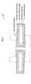
- FIG. 6is a representation of a construction of a lead frame described in the above document.
- a lead frame 900is formed by applying nickel plating 902 , palladium plating 903 , and gold-silver alloy flash plating 904 to a lead frame body 901 in this order.
- the lead frame 900 having this constructionexhibited an excellent corrosion resistance in a salt-spray test.
- this constructioncertainly has a high corrosion resistance, it has only a low light reflectance. This being so, especially when a semiconductor light-emitting element such as an LED is mounted on the lead frame to form a semiconductor light-emitting device, the lead frame cannot sufficiently reflect rear light of the light-emitting element, which impairs the luminous efficiency of the entire device.
- the present inventionwas conceived in view of the problem described above, and aims to provide a lead frame for a semiconductor device with an improved light reflectance.
- the present inventionespecially aims to provide a lead frame for a semiconductor light-emitting device.
- a lead frame for a semiconductor light-emitting deviceincluding: a lead frame body; and a plurality of metal coatings which are applied to the lead frame body, the lead frame being characterized in that: a predetermined part of the lead frame is formed by extending one pair of inner leads, which are separated by a gap, toward each other in a state where extended portions of the pair of inner leads are flat and flush with each other, the predetermined part being to be enclosed with a package of the semiconductor light-emitting device; and the plurality of metal coatings include a silver or silver-alloy coating which is an outermost metal coating of the pair of inner leads.
- the silver or silver-alloy coatingmay have a thickness of 0.1 ⁇ m or more.
- a base that is a part of the packagemay be inserted to the lead frame with a portion of the predetermined part being enclosed with the base.
- the silver or silver-alloy coatingdelivers an excellent light reflectance and wire bonding efficiency of the predetermined part which is enclosed with the package.
- the lead frameexhibits a high light reflectance in the predetermined part. Accordingly, when used in a semiconductor light-emitting device, the lead frame efficiently reflects rear light of a semiconductor light-emitting element, with it being possible to enhance the luminous efficiency of the entire device.
- the plurality of metal coatingsmay further include a gold or gold-alloy coating, a nickel or nickel-alloy coating, and a palladium or palladium-alloy coating, wherein the nickel or nickel-alloy coating, the palladium or palladium-alloy coating, the gold or gold-alloy coating, and the silver or silver-alloy coating are applied in the stated order, with the nickel or nickel-alloy coating and the palladium or palladium-alloy coating substantially entirely covering the lead frame body.
- the palladium or palladium-alloy coatinghas a high high-temperature stability, which makes the lead frame suitable for high-temperature leadless soldering.
- the plurality of metal coatingsmay further include a gold or gold-alloy coating, wherein the silver or silver-alloy coating substantially entirely covers the lead frame body, and the gold or gold-alloy coating is applied over the silver or silver-alloy coating only in a part of the lead frame other than the predetermined part.
- the gold or gold-alloy coatingpartially covers the lead frame body, whereas the silver or silver-alloy coating entirely covers the lead frame body. This simplifies the manufacturing process of the lead frame.
- the plurality of metal coatingsmay further include a nickel or nickel-alloy coating and a palladium or palladium-alloy coating, wherein the nickel or nickel-alloy coating, the palladium or palladium-alloy coating, the silver or silver-alloy coating, and the gold or gold-alloy coating are applied in the stated order, with the nickel or nickel-alloy coating and the palladium or palladium-alloy coating substantially-entirely covering the lead frame body.
- the palladium or palladium-alloy coatinghas a high high-temperature stability, which makes the lead frame suitable for high-temperature leadless soldering.
- the silver or silver-alloy coatingmay be applied except at least one part of the portion enclosed with the base.
- the adhesion between the lead frame and a resin that forms the packageis strong in the area where the silver or silver-alloy coating is absent in the predetermined part. This maintains the seal of the package and improves the resistance to corrosion in the predetermined part.
- a semiconductor light-emitting elementmay be mounted on the lead frame to form the semiconductor light-emitting device.
- the semiconductor light-emitting deviceis formed using the lead frame that has an excellent light reflectance in the predetermined part. This makes it possible to efficiently reflect rear light of the semiconductor light-emitting element, which contributes to a high luminous efficiency of the entire device.
- FIG. 1is a top view of a lead frame to which an embodiment of the invention relates.
- FIG. 2is a representation of a plating construction of the lead frame shown in FIG. 1 .
- FIG. 3is a perspective view of the lead frame after a package is formed.
- FIG. 4is a representation of a cross section of a semiconductor light-emitting device that uses the lead frame.
- FIG. 5is a graph for comparing reflectances of lead frames.
- FIG. 6is a representation of a plating construction of a conventional lead frame.
- FIG. 1is a top view of a lead frame to which the embodiment of the present invention relates.
- a lead frame 100is formed by pressing or etching a lead frame body in the illustrated pattern and then plating the lead frame body as described later.
- the lead frame bodyis a thin plate of an iron alloy or a copper alloy.
- a package for enclosing part of the lead frame 100 and housing a semiconductor element such as a semiconductor light-emitting elementis provided in each of the areas indicated by the dashed line boxes.
- the packageincludes a base and a cover.
- the basehas a depression for mounting the semiconductor light-emitting element.
- the coverseals the depression on which the semiconductor light-emitting element is mounted.
- the inner partincludes inner leads.
- reference numerals 101 a , 101 b , 101 c , 101 d , 101 e , 101 f , 101 g , and 101 hrepresent inner leads.
- the pair of inner leads 101 a and 101 bare separated by a gap and extended in a direction toward each other.
- the pair of inner leads 101 c and 101 d , the pair of inner leads 101 e and 101 f , and the pair of inner leads 101 g and 101 hare also separated by a gap and extended toward each other.
- the extended ends of the inner leads 101 a , 101 b , 101 c , 101 d , 101 e , 101 f , 101 g , and 101 hare widened as shown in the drawing. These extended ends serve as element mounting units (see FIG. 4 ). Which is to say, one semiconductor light-emitting element is to be mounted either on one of the extended ends of the pair of inner leads 101 a and 101 b or over the extended ends of the pair of inner leads 101 a and 101 b .
- the upper surfaces of the pair of inner leads 101 a and 101 bare flat and flush with each other, as illustrated.
- FIG. 2is a representation of a plating construction of the lead frame 100 , taken along the lines A-A′ in FIG. 1 .
- the lead frame 100is formed by applying nickel plating 102 , palladium plating 103 , and gold flash plating 104 to a lead frame body 101 in this order, and further applying silver plating 105 to part of the inner part.
- the nickel plating 102has a thickness of 0.5 to 2.0 ⁇ m
- the palladium plating 103has a thickness of 0.005 to 0.07 ⁇ m
- the gold flash plating 104has a thickness of 0.003 to 0.01 ⁇ m
- the silver plating 105has a thickness of 0.1 ⁇ m or more.
- these plating layersmay instead be made of alloys.
- the nickel plating 102may be nickel-alloy plating
- the palladium plating 103may be palladium-alloy plating
- the gold flash plating 104may be gold-alloy flash plating
- the silver plating 105may be silver-alloy plating.
- the base of the packageis inserted to the area indicated by the dashed lines.
- the baseis made of a white-colored or light-colored insulating resin, such as polyphthalamide.
- the basehas a depression as shown in the drawing, and releases light of the semiconductor light-emitting element placed in the depression in an upward direction. After the semiconductor light-emitting element is placed in the depression, the depression is filled with a sealing transparent resin (e.g. an epoxy resin) to form the cover.
- a sealing transparent resine.g. an epoxy resin
- the silver plating 105only partially covers the inner part, i.e., the part of the inner part enclosed with the base is partially not plated with silver.
- FIG. 3is a perspective view of the lead frame 100 after a base 200 is formed.
- FIG. 4is a representation of a cross section of a semiconductor light-emitting device 700 which uses the lead frame 100 .
- the semiconductor light-emitting device 700is formed by mounting a semiconductor light-emitting element 400 on part of the inner part exposed to the depression of the base 200 , connecting the semiconductor light-emitting element 400 with the inner part using bonding wires 500 , and then enclosing a transparent resin 300 in the depression to form a cover.
- Light 601 of the semiconductor light-emitting element 400is directly released upward, whereas other light 602 of the semiconductor light-emitting element 400 is reflected off the inner part and the base 200 and then released.
- the inventors of the present inventionconfirmed that such a constructed lead frame has the following excellent properties.
- FIG. 5is a graph for comparing light reflectances of lead frames.
- a light reflectance of a lead frame of each of sample 1 (the silver-plated lead frame part of the present invention), sample 2 (a comparative example), and sample 3 (a conventional example)was measured using a visible-ultraviolet spectrophotometer, where a light reflectance of barium sulfate is 100.
- Sample 1has the construction described above.
- Sample 2is formed by applying copper strike plating and silver plating that has a thickness of 3 ⁇ m to a copper alloy thin plate as a lead frame body, in this order. Sample 2 is used as a comparative example that can deliver a light reflectance similar to the present invention, by single-layer silver plating.
- Sample 3is a conventional lead frame. Sample 3 is formed by applying nickel plating of 1.0 to 1.2 ⁇ m in thickness, palladium plating of 0.03 ⁇ m in thickness, and gold flash plating of 0.008 ⁇ m in thickness to a copper alloy thin plate as a lead frame body, in this order.
- the silver-plated lead frame part of the present inventionhas a light reflectance that is at least 25% higher than that of the conventional example and a little higher than that of the comparative example, for visible light of 400 to 700 nm in wavelength.
- the inventors of the present inventionmeasured a shear adhesive strength of the contact surfaces of a resin which forms the base and a palladium-plated lead frame part and a shear adhesive strength of the contact surfaces of the resin and a silver-plated lead frame part. As a result, the inventors found that the shear adhesive strength of the resin and the palladium-plated lead frame part is greater than that of the resin and the silver-plated lead frame part.
- silver platingis provided only partially in the inner part, that is, silver plating is provided in the inner part except a part of the area that is enclosed with the base.
- the resinadheres to the palladium plating layer through the gold flash plating layer, in the portion of the inner part which is not plated with silver. This produces a greater shear adhesive strength than in the portion of the inner part which is plated with silver. Since the gold flash plating layer is extremely thin, it does not significantly affect the shear adhesive strength.
- the inventors of the present inventionconducted an experiment of soaking samples 1 and 2 in red ink under the same conditions. As a result, red ink did not seep into sample 1 which is not plated with silver in part of the area enclosed with the base, whilst red ink seeped into sample 2 which is entirely plated with silver.
- each of the plating layers of the lead framehas the following excellent properties.
- the silver platingnot only achieves an excellent light reflectance as described above, but also has excellent connectivity with the semiconductor light-emitting element mounted thereon and a high wire bonding efficiency.
- the gold flash platinghas a high thermal stability, which enhances the soldering efficiency of the outer part.
- the palladium platinghas a high chemical stability, and so exhibits an excellent resistance to corrosion under high-temperature environments.
- the nickel platingserves as base plating, and contributes to a high wire bonding efficiency, a high leadless soldering efficiency, a high corrosion resistance, and a high adhesive strength with the resin that forms the package.
- the lead frame of the present inventionhas a characteristic construction in which silver or silver-alloy plating is applied as the outermost coating of the inner part, to achieve a favorable light reflectance.
- this characteristic constructionis realized by coating the lead frame body substantially entirely with nickel plating, palladium plating, and gold flash plating in this order, and further coating the inner part of the lead frame with silver plating.
- the construction of the present inventioncan equally be realized by coating the lead frame body substantially entirely with nickel plating, palladium plating, and silver plating, and further coating the outer part of the lead frame with gold flash plating.
- this lead frameis included in the present invention, too.
- each of the metal coatings applied to the lead frame bodyis referred to as plating for the sake of simplicity.
- the metal coating method of the present inventionis not limited to plating.
- the metal coatingsmay be formed using a known metal coating method such as electroplating, chemical plating, evaporation, sputtering, or diffusion.
- a conventional methodsuch as masking or blasting is applicable.
- the present inventioncan be used for a semiconductor light-emitting device that requires a high luminous efficiency, such as an LED device employed in lighting, indication, decoration, communication, and the like.
Landscapes
- Physics & Mathematics (AREA)
- Condensed Matter Physics & Semiconductors (AREA)
- General Physics & Mathematics (AREA)
- Engineering & Computer Science (AREA)
- Computer Hardware Design (AREA)
- Microelectronics & Electronic Packaging (AREA)
- Power Engineering (AREA)
- Led Device Packages (AREA)
- Lead Frames For Integrated Circuits (AREA)
Abstract
Description
- The present invention relates to a lead frame for a semiconductor device, and in particular relates to techniques of improving a light reflectance of a lead frame.
- Conventionally, gold-silver alloy flash plating is formed at an outermost layer of a lead frame for a semiconductor device, to ensure a high resistance to corrosion. An example of such techniques is disclosed in Unexamined Japanese Patent Application Publication No. H11-008341.
FIG. 6 is a representation of a construction of a lead frame described in the above document. In the drawing, alead frame 900 is formed by applying nickel plating902,palladium plating 903, and gold-silveralloy flash plating 904 to alead frame body 901 in this order. According to the document, thelead frame 900 having this construction exhibited an excellent corrosion resistance in a salt-spray test.- However, though this construction certainly has a high corrosion resistance, it has only a low light reflectance. This being so, especially when a semiconductor light-emitting element such as an LED is mounted on the lead frame to form a semiconductor light-emitting device, the lead frame cannot sufficiently reflect rear light of the light-emitting element, which impairs the luminous efficiency of the entire device.
- The present invention was conceived in view of the problem described above, and aims to provide a lead frame for a semiconductor device with an improved light reflectance. The present invention especially aims to provide a lead frame for a semiconductor light-emitting device.
- The stated object can be achieved by a lead frame for a semiconductor light-emitting device, including: a lead frame body; and a plurality of metal coatings which are applied to the lead frame body, the lead frame being characterized in that: a predetermined part of the lead frame is formed by extending one pair of inner leads, which are separated by a gap, toward each other in a state where extended portions of the pair of inner leads are flat and flush with each other, the predetermined part being to be enclosed with a package of the semiconductor light-emitting device; and the plurality of metal coatings include a silver or silver-alloy coating which is an outermost metal coating of the pair of inner leads.
- Here, the silver or silver-alloy coating may have a thickness of 0.1 μm or more.
- Here, a base that is a part of the package may be inserted to the lead frame with a portion of the predetermined part being enclosed with the base.
- According to these constructions, the silver or silver-alloy coating delivers an excellent light reflectance and wire bonding efficiency of the predetermined part which is enclosed with the package.
- Thus, the lead frame exhibits a high light reflectance in the predetermined part. Accordingly, when used in a semiconductor light-emitting device, the lead frame efficiently reflects rear light of a semiconductor light-emitting element, with it being possible to enhance the luminous efficiency of the entire device.
- Here, the plurality of metal coatings may further include a gold or gold-alloy coating, a nickel or nickel-alloy coating, and a palladium or palladium-alloy coating, wherein the nickel or nickel-alloy coating, the palladium or palladium-alloy coating, the gold or gold-alloy coating, and the silver or silver-alloy coating are applied in the stated order, with the nickel or nickel-alloy coating and the palladium or palladium-alloy coating substantially entirely covering the lead frame body.
- According to this construction, the palladium or palladium-alloy coating has a high high-temperature stability, which makes the lead frame suitable for high-temperature leadless soldering.
- Here, the plurality of metal coatings may further include a gold or gold-alloy coating, wherein the silver or silver-alloy coating substantially entirely covers the lead frame body, and the gold or gold-alloy coating is applied over the silver or silver-alloy coating only in a part of the lead frame other than the predetermined part.
- According to this construction, the gold or gold-alloy coating partially covers the lead frame body, whereas the silver or silver-alloy coating entirely covers the lead frame body. This simplifies the manufacturing process of the lead frame.
- Here, the plurality of metal coatings may further include a nickel or nickel-alloy coating and a palladium or palladium-alloy coating, wherein the nickel or nickel-alloy coating, the palladium or palladium-alloy coating, the silver or silver-alloy coating, and the gold or gold-alloy coating are applied in the stated order, with the nickel or nickel-alloy coating and the palladium or palladium-alloy coating substantially-entirely covering the lead frame body.
- According to this construction, the palladium or palladium-alloy coating has a high high-temperature stability, which makes the lead frame suitable for high-temperature leadless soldering.
- Here, the silver or silver-alloy coating may be applied except at least one part of the portion enclosed with the base.
- According to this construction, the adhesion between the lead frame and a resin that forms the package is strong in the area where the silver or silver-alloy coating is absent in the predetermined part. This maintains the seal of the package and improves the resistance to corrosion in the predetermined part.
- Here, a semiconductor light-emitting element may be mounted on the lead frame to form the semiconductor light-emitting device.
- According to this construction, the semiconductor light-emitting device is formed using the lead frame that has an excellent light reflectance in the predetermined part. This makes it possible to efficiently reflect rear light of the semiconductor light-emitting element, which contributes to a high luminous efficiency of the entire device.
FIG. 1 is a top view of a lead frame to which an embodiment of the invention relates.FIG. 2 is a representation of a plating construction of the lead frame shown inFIG. 1 .FIG. 3 is a perspective view of the lead frame after a package is formed.FIG. 4 is a representation of a cross section of a semiconductor light-emitting device that uses the lead frame.FIG. 5 is a graph for comparing reflectances of lead frames.FIG. 6 is a representation of a plating construction of a conventional lead frame.- An embodiment of the present invention is described in detail below, by referring to the drawings.
- (Pattern of a Lead Frame)
FIG. 1 is a top view of a lead frame to which the embodiment of the present invention relates.- In the drawing, a
lead frame 100 is formed by pressing or etching a lead frame body in the illustrated pattern and then plating the lead frame body as described later. For example, the lead frame body is a thin plate of an iron alloy or a copper alloy. - A package for enclosing part of the
lead frame 100 and housing a semiconductor element such as a semiconductor light-emitting element is provided in each of the areas indicated by the dashed line boxes. The package includes a base and a cover. The base has a depression for mounting the semiconductor light-emitting element. The cover seals the depression on which the semiconductor light-emitting element is mounted. - In this specification, a part of the
lead frame 100 which is inside each of the areas indicated by the dashed line boxes, i.e. which is enclosed with the package, is called an inner part, whereas a part of thelead frame 100 which is outside the package is called an outer part. The inner part includes inner leads. InFIG. 1 ,reference numerals inner leads inner leads inner leads inner leads inner leads FIG. 4 ). Which is to say, one semiconductor light-emitting element is to be mounted either on one of the extended ends of the pair ofinner leads inner leads inner leads inner leads inner leads inner leads - (Plating)
FIG. 2 is a representation of a plating construction of thelead frame 100, taken along the lines A-A′ inFIG. 1 .- The
lead frame 100 is formed by applying nickel plating102, palladium plating103, and gold flash plating104 to alead frame body 101 in this order, and further applyingsilver plating 105 to part of the inner part. - For example, the
nickel plating 102 has a thickness of 0.5 to 2.0 μm, thepalladium plating 103 has a thickness of 0.005 to 0.07 μm, thegold flash plating 104 has a thickness of 0.003 to 0.01 μm, and thesilver plating 105 has a thickness of 0.1 μm or more. - Here, these plating layers may instead be made of alloys. Which is to say, the nickel plating102 may be nickel-alloy plating, the palladium plating103 may be palladium-alloy plating, the gold flash plating104 may be gold-alloy flash plating, and the
silver plating 105 may be silver-alloy plating. - After plating, the base of the package is inserted to the area indicated by the dashed lines. The base is made of a white-colored or light-colored insulating resin, such as polyphthalamide. The base has a depression as shown in the drawing, and releases light of the semiconductor light-emitting element placed in the depression in an upward direction. After the semiconductor light-emitting element is placed in the depression, the depression is filled with a sealing transparent resin (e.g. an epoxy resin) to form the cover. The base and the cover together constitute the package.
- It should be noted here that the silver plating105 only partially covers the inner part, i.e., the part of the inner part enclosed with the base is partially not plated with silver.
- (Semiconductor Device Using the Lead Frame100)
FIG. 3 is a perspective view of thelead frame 100 after abase 200 is formed.FIG. 4 is a representation of a cross section of a semiconductor light-emittingdevice 700 which uses thelead frame 100.- The semiconductor light-emitting
device 700 is formed by mounting a semiconductor light-emittingelement 400 on part of the inner part exposed to the depression of thebase 200, connecting the semiconductor light-emittingelement 400 with the inner part usingbonding wires 500, and then enclosing atransparent resin 300 in the depression to form a cover. Light 601 of the semiconductor light-emittingelement 400 is directly released upward, whereasother light 602 of the semiconductor light-emittingelement 400 is reflected off the inner part and thebase 200 and then released.- The inventors of the present invention confirmed that such a constructed lead frame has the following excellent properties.
- (Light Reflectance)
FIG. 5 is a graph for comparing light reflectances of lead frames. A light reflectance of a lead frame of each of sample 1 (the silver-plated lead frame part of the present invention), sample 2 (a comparative example), and sample 3 (a conventional example) was measured using a visible-ultraviolet spectrophotometer, where a light reflectance of barium sulfate is 100.Sample 1 has the construction described above.Sample 2 is formed by applying copper strike plating and silver plating that has a thickness of 3 μm to a copper alloy thin plate as a lead frame body, in this order.Sample 2 is used as a comparative example that can deliver a light reflectance similar to the present invention, by single-layer silver plating.Sample 3 is a conventional lead frame.Sample 3 is formed by applying nickel plating of 1.0 to 1.2 μm in thickness, palladium plating of 0.03 μm in thickness, and gold flash plating of 0.008 μm in thickness to a copper alloy thin plate as a lead frame body, in this order.- As shown in the graph, the silver-plated lead frame part of the present invention has a light reflectance that is at least 25% higher than that of the conventional example and a little higher than that of the comparative example, for visible light of 400 to 700 nm in wavelength.
- (Resin Adhesiveness)
- Also, the inventors of the present invention measured a shear adhesive strength of the contact surfaces of a resin which forms the base and a palladium-plated lead frame part and a shear adhesive strength of the contact surfaces of the resin and a silver-plated lead frame part. As a result, the inventors found that the shear adhesive strength of the resin and the palladium-plated lead frame part is greater than that of the resin and the silver-plated lead frame part. In view of this, silver plating is provided only partially in the inner part, that is, silver plating is provided in the inner part except a part of the area that is enclosed with the base.
- As a result, the resin adheres to the palladium plating layer through the gold flash plating layer, in the portion of the inner part which is not plated with silver. This produces a greater shear adhesive strength than in the portion of the inner part which is plated with silver. Since the gold flash plating layer is extremely thin, it does not significantly affect the shear adhesive strength.
- The inventors of the present invention conducted an experiment of soaking
samples sample 1 which is not plated with silver in part of the area enclosed with the base, whilst red ink seeped intosample 2 which is entirely plated with silver. - (Other Properties)
- In addition, each of the plating layers of the lead frame has the following excellent properties.
- The silver plating not only achieves an excellent light reflectance as described above, but also has excellent connectivity with the semiconductor light-emitting element mounted thereon and a high wire bonding efficiency.
- The gold flash plating has a high thermal stability, which enhances the soldering efficiency of the outer part.
- The palladium plating has a high chemical stability, and so exhibits an excellent resistance to corrosion under high-temperature environments.
- The nickel plating serves as base plating, and contributes to a high wire bonding efficiency, a high leadless soldering efficiency, a high corrosion resistance, and a high adhesive strength with the resin that forms the package.
- As described above, the lead frame of the present invention has a characteristic construction in which silver or silver-alloy plating is applied as the outermost coating of the inner part, to achieve a favorable light reflectance.
- In the above embodiment, this characteristic construction is realized by coating the lead frame body substantially entirely with nickel plating, palladium plating, and gold flash plating in this order, and further coating the inner part of the lead frame with silver plating. However, the construction of the present invention can equally be realized by coating the lead frame body substantially entirely with nickel plating, palladium plating, and silver plating, and further coating the outer part of the lead frame with gold flash plating. Hence this lead frame is included in the present invention, too.
- In the above embodiment, each of the metal coatings applied to the lead frame body is referred to as plating for the sake of simplicity. However, the metal coating method of the present invention is not limited to plating. For example, the metal coatings may be formed using a known metal coating method such as electroplating, chemical plating, evaporation, sputtering, or diffusion.
- Here, to coat a desired area with a metal, a conventional method such as masking or blasting is applicable.
- The present invention can be used for a semiconductor light-emitting device that requires a high luminous efficiency, such as an LED device employed in lighting, indication, decoration, communication, and the like.
Claims (10)
Priority Applications (2)
| Application Number | Priority Date | Filing Date | Title |
|---|---|---|---|
| US12/509,065US7994616B2 (en) | 2003-01-16 | 2009-07-24 | Multilayered lead frame for a semiconductor light-emitting device |
| US12/716,938US8541871B2 (en) | 2003-01-16 | 2010-03-03 | Multilayered lead frame for a semiconductor light-emitting device |
Applications Claiming Priority (3)
| Application Number | Priority Date | Filing Date | Title |
|---|---|---|---|
| JP2003007988 | 2003-01-16 | ||
| JP2003-007988 | 2003-01-16 | ||
| PCT/JP2004/000152WO2004064154A1 (en) | 2003-01-16 | 2004-01-13 | Lead frame for a semiconductor device |
Related Child Applications (2)
| Application Number | Title | Priority Date | Filing Date |
|---|---|---|---|
| US12/509,065DivisionUS7994616B2 (en) | 2003-01-16 | 2009-07-24 | Multilayered lead frame for a semiconductor light-emitting device |
| US12/716,938DivisionUS8541871B2 (en) | 2003-01-16 | 2010-03-03 | Multilayered lead frame for a semiconductor light-emitting device |
Publications (2)
| Publication Number | Publication Date |
|---|---|
| US20060102936A1true US20060102936A1 (en) | 2006-05-18 |
| US7692277B2 US7692277B2 (en) | 2010-04-06 |
Family
ID=32709142
Family Applications (3)
| Application Number | Title | Priority Date | Filing Date |
|---|---|---|---|
| US10/542,419Expired - LifetimeUS7692277B2 (en) | 2003-01-16 | 2004-01-13 | Multilayered lead frame for a semiconductor light-emitting device |
| US12/509,065Expired - LifetimeUS7994616B2 (en) | 2003-01-16 | 2009-07-24 | Multilayered lead frame for a semiconductor light-emitting device |
| US12/716,938Expired - LifetimeUS8541871B2 (en) | 2003-01-16 | 2010-03-03 | Multilayered lead frame for a semiconductor light-emitting device |
Family Applications After (2)
| Application Number | Title | Priority Date | Filing Date |
|---|---|---|---|
| US12/509,065Expired - LifetimeUS7994616B2 (en) | 2003-01-16 | 2009-07-24 | Multilayered lead frame for a semiconductor light-emitting device |
| US12/716,938Expired - LifetimeUS8541871B2 (en) | 2003-01-16 | 2010-03-03 | Multilayered lead frame for a semiconductor light-emitting device |
Country Status (7)
| Country | Link |
|---|---|
| US (3) | US7692277B2 (en) |
| KR (1) | KR101059361B1 (en) |
| CN (2) | CN101546803B (en) |
| DE (1) | DE112004000155B4 (en) |
| MY (1) | MY144642A (en) |
| TW (1) | TWI264105B (en) |
| WO (1) | WO2004064154A1 (en) |
Cited By (8)
| Publication number | Priority date | Publication date | Assignee | Title |
|---|---|---|---|---|
| US20060147746A1 (en)* | 2004-12-03 | 2006-07-06 | Ngk Spark Plug Co., Ltd. | Ceramic substrate, ceramic package for housing light emitting element |
| US20060255357A1 (en)* | 2005-05-11 | 2006-11-16 | Sharp Kabushiki Kaisha | Light emitting element mounting frame and light emitting device |
| US20080194048A1 (en)* | 2007-02-13 | 2008-08-14 | Bily Wang | Method for manufacturing a light-emitting diode having high heat-dissipating efficiency |
| US20120175657A1 (en)* | 2011-01-11 | 2012-07-12 | Lextar Electronics Corporation | Light-emitting diode lamp with an improved leadframe |
| US20120299172A1 (en)* | 2011-05-27 | 2012-11-29 | Joon Su Kim | Lead frame for semiconductor device |
| US20130099270A1 (en)* | 2010-06-15 | 2013-04-25 | Furukawa Electric Co., Ltd. | Lead frame for optical semiconductor device, method of producing the same, and optical semiconductor device |
| TWI479704B (en)* | 2008-12-26 | 2015-04-01 | Furukawa Electric Co Ltd | A lead frame for an optical semiconductor device, a method for manufacturing the same, and an optical semiconductor device |
| TWI891100B (en)* | 2023-08-31 | 2025-07-21 | 南韓商麥肯化工科技股份有限公司 | Semiconductor package substrate and semiconductor package including the same |
Families Citing this family (26)
| Publication number | Priority date | Publication date | Assignee | Title |
|---|---|---|---|---|
| JP4820616B2 (en)* | 2005-10-20 | 2011-11-24 | パナソニック株式会社 | Lead frame |
| JP2008091818A (en)* | 2006-10-05 | 2008-04-17 | Matsushita Electric Ind Co Ltd | Lead frame for optical semiconductor device, optical semiconductor device using the same, and manufacturing method thereof |
| JP4834022B2 (en)* | 2007-03-27 | 2011-12-07 | 古河電気工業株式会社 | Silver coating material for movable contact parts and manufacturing method thereof |
| KR101485319B1 (en)* | 2008-06-30 | 2015-01-22 | 서울반도체 주식회사 | Light emitting device |
| JP2010045140A (en)* | 2008-08-11 | 2010-02-25 | Nec Electronics Corp | Lead frame, method of manufacturing the same, and method of manufacturing semiconductor device |
| KR101509228B1 (en)* | 2008-09-17 | 2015-04-10 | 서울반도체 주식회사 | Side-view led package having thinner outer lead than inner lead and method of fabrication the same |
| WO2010035944A2 (en)* | 2008-09-29 | 2010-04-01 | 서울반도체 주식회사 | Light-emitting device |
| WO2010071182A1 (en)* | 2008-12-19 | 2010-06-24 | 古河電気工業株式会社 | Optical semiconductor device lead frame and manufacturing method thereof |
| KR101081920B1 (en)* | 2009-07-07 | 2011-11-10 | 서울반도체 주식회사 | Light emitting device |
| CN101867009B (en)* | 2010-05-07 | 2014-10-15 | 厦门永红科技有限公司 | LED lead frame and electroplating method and electroplating equipment thereof |
| KR101802850B1 (en) | 2011-01-11 | 2017-11-29 | 해성디에스 주식회사 | Semiconductor package |
| JP5682341B2 (en)* | 2011-02-01 | 2015-03-11 | 日亜化学工業株式会社 | Light emitting device and manufacturing method thereof |
| US8846421B2 (en)* | 2011-03-10 | 2014-09-30 | Mds Co. Ltd. | Method of manufacturing lead frame for light-emitting device package and light-emitting device package |
| DE102011083691B4 (en)* | 2011-09-29 | 2020-03-12 | Osram Gmbh | OPTOELECTRONIC SEMICONDUCTOR COMPONENT |
| US20130098659A1 (en)* | 2011-10-25 | 2013-04-25 | Yiu Fai KWAN | Pre-plated lead frame for copper wire bonding |
| TWI483437B (en)* | 2012-03-27 | 2015-05-01 | Lextar Electronics Corp | Light emitting diode package and method for fabricating the same |
| TWI447961B (en)* | 2012-04-16 | 2014-08-01 | Lextar Electronics Corp | Light-emitting diode package |
| CN102956795A (en)* | 2012-07-17 | 2013-03-06 | 孙百贵 | TOP LED (Light Emitting Diode) metal support and manufacturing method thereof |
| CN102903823A (en)* | 2012-07-17 | 2013-01-30 | 孙百贵 | Novel TOP LED (Light-Emitting Diode) metal bracket and manufacturing method thereof |
| KR101802851B1 (en) | 2013-03-11 | 2017-11-29 | 해성디에스 주식회사 | Lead frame, semiconductor package including the lead frame, and method of manufacturing the lead frame |
| KR101511032B1 (en)* | 2013-09-25 | 2015-04-10 | 앰코 테크놀로지 코리아 주식회사 | Leadframe for manufacturing LED package and LED package using the same |
| DE102014101155A1 (en)* | 2014-01-30 | 2015-07-30 | Osram Opto Semiconductors Gmbh | Optoelectronic component |
| DE102014101154A1 (en)* | 2014-01-30 | 2015-07-30 | Osram Opto Semiconductors Gmbh | Optoelectronic arrangement |
| CN110265376A (en) | 2018-03-12 | 2019-09-20 | 意法半导体股份有限公司 | Lead frame surface finishing |
| US11735512B2 (en) | 2018-12-31 | 2023-08-22 | Stmicroelectronics International N.V. | Leadframe with a metal oxide coating and method of forming the same |
| US12351936B2 (en) | 2022-05-19 | 2025-07-08 | Te Connectivity Solutions Gmbh | Layered plating stack for improved contact resistance in corrosive environments |
Citations (8)
| Publication number | Priority date | Publication date | Assignee | Title |
|---|---|---|---|---|
| US4979017A (en)* | 1989-02-23 | 1990-12-18 | Adam Mii | Semiconductor element string structure |
| US5424578A (en)* | 1993-01-29 | 1995-06-13 | Sharp Kabushiki Kaisha | Lead frame for use in a semiconductor device and a semiconductor device using the same |
| US5670797A (en)* | 1994-12-06 | 1997-09-23 | Sharp Kabushiki Kaisha | Compact light-emitting device with sealing member and light-transmitting resin seal |
| US5936264A (en)* | 1996-11-15 | 1999-08-10 | Rohm Co., Ltd. | Mounting technique for a chip light emitting device |
| US20010022390A1 (en)* | 1998-06-30 | 2001-09-20 | Gunther Waitl | Diode housing |
| US6352634B1 (en)* | 1998-06-10 | 2002-03-05 | W. C. Heraeus Gmbh & Co. Kg | Method for producing a lead-free substrate |
| US20020047186A1 (en)* | 2000-07-13 | 2002-04-25 | Tellkamp John P. | Semiconductor leadframes comprising silver plating |
| US20040089898A1 (en)* | 2002-06-28 | 2004-05-13 | Osram Opto Semiconductors Gmbh | Optoelectronic component and method for producing it |
Family Cites Families (20)
| Publication number | Priority date | Publication date | Assignee | Title |
|---|---|---|---|---|
| JPS6178150A (en)* | 1984-09-25 | 1986-04-21 | Sumitomo Electric Ind Ltd | Lead frame for resin-sealed semiconductor devices |
| JPS61148883A (en) | 1984-12-22 | 1986-07-07 | Toshiba Corp | Lead frame for optical semiconductor devices |
| JP2596542B2 (en)* | 1986-05-12 | 1997-04-02 | 株式会社日立製作所 | Lead frame and semiconductor device using the same |
| JPH01305551A (en)* | 1988-06-03 | 1989-12-08 | Kobe Steel Ltd | Lead frame for semiconductor device and semiconductor device |
| US5227662A (en)* | 1990-05-24 | 1993-07-13 | Nippon Steel Corporation | Composite lead frame and semiconductor device using the same |
| US5384155A (en)* | 1992-06-04 | 1995-01-24 | Texas Instruments Incorporated | Silver spot/palladium plate lead frame finish |
| JPH0714962A (en)* | 1993-04-28 | 1995-01-17 | Mitsubishi Shindoh Co Ltd | Lead frame material and lead frame |
| KR100231828B1 (en) | 1997-02-20 | 1999-12-01 | 유무성 | Multi-layer plated lead frame |
| TW448204B (en)* | 1997-04-09 | 2001-08-01 | Jeng Wu Shuen | A method for catalytic depolymerization of polyethylene terephthalate |
| JPH118341A (en)* | 1997-06-18 | 1999-01-12 | Mitsui High Tec Inc | Lead frame for semiconductor device |
| JP3908383B2 (en)* | 1998-05-29 | 2007-04-25 | ローム株式会社 | Semiconductor device |
| DE19850526C2 (en)* | 1998-11-03 | 2002-11-28 | Heraeus Gmbh W C | Metallic coating substrate and its use |
| JP2002335012A (en) | 1999-02-25 | 2002-11-22 | Nichia Chem Ind Ltd | Light emitting diode and dot matrix display using the same |
| WO2000062341A1 (en)* | 1999-04-08 | 2000-10-19 | Shinko Electric Industries Co., Ltd. | Lead frame for semiconductor device |
| JP2001127229A (en)* | 1999-11-01 | 2001-05-11 | Nec Corp | Lead frame and resin-sealed semiconductor device provided therewith |
| JP4432275B2 (en)* | 2000-07-13 | 2010-03-17 | パナソニック電工株式会社 | Light source device |
| JP2002060122A (en) | 2000-08-15 | 2002-02-26 | Canon Aptex Inc | Sheet sheaf binder and image forming device provided therewith |
| DE60137972D1 (en) | 2001-04-12 | 2009-04-23 | Matsushita Electric Works Ltd | LIGHT SOURCE ELEMENT WITH LED AND METHOD FOR THE PRODUCTION THEREOF |
| TWI302758B (en)* | 2006-04-21 | 2008-11-01 | Silicon Base Dev Inc | Package base structure of photo diode and manufacturing method of the same |
| KR100854328B1 (en)* | 2006-07-07 | 2008-08-28 | 엘지전자 주식회사 | Light emitting device package and its manufacturing method |
- 2004
- 2004-01-13CNCN2009101347600Apatent/CN101546803B/ennot_activeExpired - Lifetime
- 2004-01-13CNCNB2004800021943Apatent/CN100499099C/ennot_activeExpired - Lifetime
- 2004-01-13WOPCT/JP2004/000152patent/WO2004064154A1/ennot_activeCeased
- 2004-01-13USUS10/542,419patent/US7692277B2/ennot_activeExpired - Lifetime
- 2004-01-13DEDE112004000155.2Tpatent/DE112004000155B4/ennot_activeExpired - Lifetime
- 2004-01-13KRKR1020057012373Apatent/KR101059361B1/ennot_activeExpired - Lifetime
- 2004-01-15MYMYPI20040108Apatent/MY144642A/enunknown
- 2004-01-15TWTW093101058Apatent/TWI264105B/ennot_activeIP Right Cessation
- 2009
- 2009-07-24USUS12/509,065patent/US7994616B2/ennot_activeExpired - Lifetime
- 2010
- 2010-03-03USUS12/716,938patent/US8541871B2/ennot_activeExpired - Lifetime
Patent Citations (8)
| Publication number | Priority date | Publication date | Assignee | Title |
|---|---|---|---|---|
| US4979017A (en)* | 1989-02-23 | 1990-12-18 | Adam Mii | Semiconductor element string structure |
| US5424578A (en)* | 1993-01-29 | 1995-06-13 | Sharp Kabushiki Kaisha | Lead frame for use in a semiconductor device and a semiconductor device using the same |
| US5670797A (en)* | 1994-12-06 | 1997-09-23 | Sharp Kabushiki Kaisha | Compact light-emitting device with sealing member and light-transmitting resin seal |
| US5936264A (en)* | 1996-11-15 | 1999-08-10 | Rohm Co., Ltd. | Mounting technique for a chip light emitting device |
| US6352634B1 (en)* | 1998-06-10 | 2002-03-05 | W. C. Heraeus Gmbh & Co. Kg | Method for producing a lead-free substrate |
| US20010022390A1 (en)* | 1998-06-30 | 2001-09-20 | Gunther Waitl | Diode housing |
| US20020047186A1 (en)* | 2000-07-13 | 2002-04-25 | Tellkamp John P. | Semiconductor leadframes comprising silver plating |
| US20040089898A1 (en)* | 2002-06-28 | 2004-05-13 | Osram Opto Semiconductors Gmbh | Optoelectronic component and method for producing it |
Cited By (13)
| Publication number | Priority date | Publication date | Assignee | Title |
|---|---|---|---|---|
| US7648775B2 (en) | 2004-12-03 | 2010-01-19 | Ngk Spark Plug Co., Ltd. | Ceramic substrate, ceramic package for housing light emitting element |
| US20060147746A1 (en)* | 2004-12-03 | 2006-07-06 | Ngk Spark Plug Co., Ltd. | Ceramic substrate, ceramic package for housing light emitting element |
| US20060255357A1 (en)* | 2005-05-11 | 2006-11-16 | Sharp Kabushiki Kaisha | Light emitting element mounting frame and light emitting device |
| US20080194048A1 (en)* | 2007-02-13 | 2008-08-14 | Bily Wang | Method for manufacturing a light-emitting diode having high heat-dissipating efficiency |
| US7749781B2 (en)* | 2007-02-13 | 2010-07-06 | Harvatek Corporation | Method for manufacturing a light-emitting diode having high heat-dissipating efficiency |
| TWI479704B (en)* | 2008-12-26 | 2015-04-01 | Furukawa Electric Co Ltd | A lead frame for an optical semiconductor device, a method for manufacturing the same, and an optical semiconductor device |
| US20130099270A1 (en)* | 2010-06-15 | 2013-04-25 | Furukawa Electric Co., Ltd. | Lead frame for optical semiconductor device, method of producing the same, and optical semiconductor device |
| CN102593334A (en)* | 2011-01-11 | 2012-07-18 | 隆达电子股份有限公司 | Lead frame, packaging cup with lead frame and light-emitting diode lamp |
| US8610150B2 (en)* | 2011-01-11 | 2013-12-17 | Lextar Electronics Corporation | Light-emitting diode lamp with an improved leadframe |
| US20120175657A1 (en)* | 2011-01-11 | 2012-07-12 | Lextar Electronics Corporation | Light-emitting diode lamp with an improved leadframe |
| US20120299172A1 (en)* | 2011-05-27 | 2012-11-29 | Joon Su Kim | Lead frame for semiconductor device |
| US9472494B2 (en)* | 2011-05-27 | 2016-10-18 | Amkor Technology, Inc. | Lead frame for semiconductor device |
| TWI891100B (en)* | 2023-08-31 | 2025-07-21 | 南韓商麥肯化工科技股份有限公司 | Semiconductor package substrate and semiconductor package including the same |
Also Published As
| Publication number | Publication date |
|---|---|
| DE112004000155T5 (en) | 2008-03-20 |
| MY144642A (en) | 2011-10-31 |
| KR20050097926A (en) | 2005-10-10 |
| US7692277B2 (en) | 2010-04-06 |
| CN101546803B (en) | 2010-12-08 |
| CN101546803A (en) | 2009-09-30 |
| DE112004000155B4 (en) | 2019-06-19 |
| US8541871B2 (en) | 2013-09-24 |
| TW200416993A (en) | 2004-09-01 |
| US7994616B2 (en) | 2011-08-09 |
| US20090283791A1 (en) | 2009-11-19 |
| KR101059361B1 (en) | 2011-08-24 |
| WO2004064154A1 (en) | 2004-07-29 |
| CN100499099C (en) | 2009-06-10 |
| US20100155770A1 (en) | 2010-06-24 |
| TWI264105B (en) | 2006-10-11 |
| CN1795554A (en) | 2006-06-28 |
Similar Documents
| Publication | Publication Date | Title |
|---|---|---|
| US8541871B2 (en) | Multilayered lead frame for a semiconductor light-emitting device | |
| US10263166B2 (en) | Light emitting device | |
| CN102804428B (en) | Lead frame or substrate for LED, semiconductor device, and method for manufacturing lead frame or substrate for LED | |
| US7956469B2 (en) | Light emitting device and method of manufacturing the same | |
| CN102318090B (en) | Encapsulated optoelectronic semiconductor device with solder stop layer and corresponding method | |
| US20080098594A1 (en) | Leadframes for Improved Moisture Reliability of Semiconductor Devices | |
| JP3940124B2 (en) | apparatus | |
| JP7148792B2 (en) | METAL MATERIAL FOR OPTO-SEMICONDUCTOR DEVICE, MANUFACTURING METHOD THEREOF, AND OPTO-SEMICONDUCTOR DEVICE USING THE SAME | |
| US9755123B2 (en) | Light emitting device and method of manufacturing the light emitting device | |
| JP2004207672A (en) | Light emitting element storage package and light emitting device | |
| JP2011228687A (en) | Led lead frame or substrate, semiconductor device, and method of manufacturing led lead frame or substrate | |
| US20230002637A1 (en) | Method of manufacturing metal structure for optical semiconductor device, package, and solution containing polyallylamine polymer | |
| JP2010206034A (en) | Lead frame for optical semiconductor device, package for the optical semiconductor device, the optical semiconductor device, production method of lead frame for optical semiconductor device, production method of package for the optical semiconductor device, and production method of the optical semiconductor device | |
| US20040251828A1 (en) | LED lamp and method for manufacturing the same | |
| JPH08330497A (en) | Lead frame and semiconductor device using the same | |
| KR101863545B1 (en) | Semiconductor light emitting device | |
| JP2020053601A (en) | Metal material for optical semiconductor device, method of manufacturing the same, and optical semiconductor device using the same | |
| JP2011129658A (en) | Lead frame for optical semiconductor device, method for manufacturing the same, and optical semiconductor device | |
| JP7148793B2 (en) | METAL MATERIAL FOR OPTO-SEMICONDUCTOR DEVICE, MANUFACTURING METHOD THEREOF, AND OPTO-SEMICONDUCTOR DEVICE USING THE SAME | |
| JP3088421U (en) | Optical semiconductor | |
| JP2019044261A (en) | Lead frame, package for light-emitting device, light-emitting device, and method of manufacturing light-emitting device | |
| TW201919855A (en) | Light-emitting device |
Legal Events
| Date | Code | Title | Description |
|---|---|---|---|
| AS | Assignment | Owner name:MATSUSHITA ELECTRIC INDUSTRIAL CO., LTD.,JAPAN Free format text:ASSIGNMENT OF ASSIGNORS INTEREST;ASSIGNORS:TOMOHIRO, HIDEKAZU;FUJII, MASAYUKI;SATOU, NORIO;AND OTHERS;SIGNING DATES FROM 20050830 TO 20050907;REEL/FRAME:017485/0021 Owner name:MATSUSHITA ELECTRIC INDUSTRIAL CO., LTD., JAPAN Free format text:ASSIGNMENT OF ASSIGNORS INTEREST;ASSIGNORS:TOMOHIRO, HIDEKAZU;FUJII, MASAYUKI;SATOU, NORIO;AND OTHERS;REEL/FRAME:017485/0021;SIGNING DATES FROM 20050830 TO 20050907 | |
| AS | Assignment | Owner name:PANASONIC CORPORATION,JAPAN Free format text:CHANGE OF NAME;ASSIGNOR:MATSUSHITA ELECTRIC INDUSTRIAL CO., LTD.;REEL/FRAME:021897/0570 Effective date:20081001 Owner name:PANASONIC CORPORATION, JAPAN Free format text:CHANGE OF NAME;ASSIGNOR:MATSUSHITA ELECTRIC INDUSTRIAL CO., LTD.;REEL/FRAME:021897/0570 Effective date:20081001 | |
| STCF | Information on status: patent grant | Free format text:PATENTED CASE | |
| FEPP | Fee payment procedure | Free format text:PAYOR NUMBER ASSIGNED (ORIGINAL EVENT CODE: ASPN); ENTITY STATUS OF PATENT OWNER: LARGE ENTITY | |
| FPAY | Fee payment | Year of fee payment:4 | |
| MAFP | Maintenance fee payment | Free format text:PAYMENT OF MAINTENANCE FEE, 8TH YEAR, LARGE ENTITY (ORIGINAL EVENT CODE: M1552) Year of fee payment:8 | |
| MAFP | Maintenance fee payment | Free format text:PAYMENT OF MAINTENANCE FEE, 12TH YEAR, LARGE ENTITY (ORIGINAL EVENT CODE: M1553); ENTITY STATUS OF PATENT OWNER: LARGE ENTITY Year of fee payment:12 | |
| AS | Assignment | Owner name:PANASONIC HOLDINGS CORPORATION, JAPAN Free format text:CHANGE OF NAME;ASSIGNOR:PANASONIC CORPORATION;REEL/FRAME:061362/0441 Effective date:20220401 |