US20060101370A1 - Method for improving optical proximity correction - Google Patents
Method for improving optical proximity correctionDownload PDFInfo
- Publication number
- US20060101370A1 US20060101370A1US10/904,355US90435504AUS2006101370A1US 20060101370 A1US20060101370 A1US 20060101370A1US 90435504 AUS90435504 AUS 90435504AUS 2006101370 A1US2006101370 A1US 2006101370A1
- Authority
- US
- United States
- Prior art keywords
- pattern
- model
- computer
- wafer
- mask
- Prior art date
- Legal status (The legal status is an assumption and is not a legal conclusion. Google has not performed a legal analysis and makes no representation as to the accuracy of the status listed.)
- Granted
Links
- 238000000034methodMethods0.000titleclaimsabstractdescription205
- 238000012937correctionMethods0.000titleclaimsabstractdescription25
- 230000003287optical effectEffects0.000titleclaimsabstractdescription23
- 230000008569processEffects0.000claimsabstractdescription155
- 238000013461designMethods0.000claimsabstractdescription83
- 238000004088simulationMethods0.000claimsabstractdescription40
- 230000001419dependent effectEffects0.000claimsabstractdescription32
- 238000012360testing methodMethods0.000claimsdescription25
- 238000004590computer programMethods0.000claims12
- 235000012431wafersNutrition0.000description46
- 238000001459lithographyMethods0.000description14
- 239000004065semiconductorSubstances0.000description12
- 239000010410layerSubstances0.000description9
- 230000000694effectsEffects0.000description8
- 238000004519manufacturing processMethods0.000description7
- 238000012545processingMethods0.000description6
- 238000009826distributionMethods0.000description4
- 238000007639printingMethods0.000description4
- 238000010586diagramMethods0.000description3
- 239000011295pitchSubstances0.000description3
- XUIMIQQOPSSXEZ-UHFFFAOYSA-NSiliconChemical compound[Si]XUIMIQQOPSSXEZ-UHFFFAOYSA-N0.000description2
- 238000000354decomposition reactionMethods0.000description2
- 238000011161developmentMethods0.000description2
- 230000018109developmental processEffects0.000description2
- 230000006872improvementEffects0.000description2
- 239000000463materialSubstances0.000description2
- 229920002120photoresistant polymerPolymers0.000description2
- 229910021420polycrystalline siliconInorganic materials0.000description2
- 229920005591polysiliconPolymers0.000description2
- 238000000926separation methodMethods0.000description2
- 229910052710siliconInorganic materials0.000description2
- 239000010703siliconSubstances0.000description2
- 230000009466transformationEffects0.000description2
- VYZAMTAEIAYCRO-UHFFFAOYSA-NChromiumChemical compound[Cr]VYZAMTAEIAYCRO-UHFFFAOYSA-N0.000description1
- 230000004075alterationEffects0.000description1
- 230000015572biosynthetic processEffects0.000description1
- 230000002925chemical effectEffects0.000description1
- 238000007796conventional methodMethods0.000description1
- 230000007547defectEffects0.000description1
- 238000012938design processMethods0.000description1
- 238000005516engineering processMethods0.000description1
- 238000003384imaging methodMethods0.000description1
- 238000012804iterative processMethods0.000description1
- 230000001151other effectEffects0.000description1
- 230000010363phase shiftEffects0.000description1
- 238000000206photolithographyMethods0.000description1
- 230000000704physical effectEffects0.000description1
- 238000005498polishingMethods0.000description1
- 238000002360preparation methodMethods0.000description1
- 230000011218segmentationEffects0.000description1
- 239000002356single layerSubstances0.000description1
- 238000006467substitution reactionMethods0.000description1
Images


Classifications
- G—PHYSICS
- G03—PHOTOGRAPHY; CINEMATOGRAPHY; ANALOGOUS TECHNIQUES USING WAVES OTHER THAN OPTICAL WAVES; ELECTROGRAPHY; HOLOGRAPHY
- G03F—PHOTOMECHANICAL PRODUCTION OF TEXTURED OR PATTERNED SURFACES, e.g. FOR PRINTING, FOR PROCESSING OF SEMICONDUCTOR DEVICES; MATERIALS THEREFOR; ORIGINALS THEREFOR; APPARATUS SPECIALLY ADAPTED THEREFOR
- G03F7/00—Photomechanical, e.g. photolithographic, production of textured or patterned surfaces, e.g. printing surfaces; Materials therefor, e.g. comprising photoresists; Apparatus specially adapted therefor
- G03F7/70—Microphotolithographic exposure; Apparatus therefor
- G03F7/70425—Imaging strategies, e.g. for increasing throughput or resolution, printing product fields larger than the image field or compensating lithography- or non-lithography errors, e.g. proximity correction, mix-and-match, stitching or double patterning
- G03F7/70433—Layout for increasing efficiency or for compensating imaging errors, e.g. layout of exposure fields for reducing focus errors; Use of mask features for increasing efficiency or for compensating imaging errors
- G03F7/70441—Optical proximity correction [OPC]
- G—PHYSICS
- G03—PHOTOGRAPHY; CINEMATOGRAPHY; ANALOGOUS TECHNIQUES USING WAVES OTHER THAN OPTICAL WAVES; ELECTROGRAPHY; HOLOGRAPHY
- G03F—PHOTOMECHANICAL PRODUCTION OF TEXTURED OR PATTERNED SURFACES, e.g. FOR PRINTING, FOR PROCESSING OF SEMICONDUCTOR DEVICES; MATERIALS THEREFOR; ORIGINALS THEREFOR; APPARATUS SPECIALLY ADAPTED THEREFOR
- G03F1/00—Originals for photomechanical production of textured or patterned surfaces, e.g., masks, photo-masks, reticles; Mask blanks or pellicles therefor; Containers specially adapted therefor; Preparation thereof
- G03F1/36—Masks having proximity correction features; Preparation thereof, e.g. optical proximity correction [OPC] design processes
- G—PHYSICS
- G03—PHOTOGRAPHY; CINEMATOGRAPHY; ANALOGOUS TECHNIQUES USING WAVES OTHER THAN OPTICAL WAVES; ELECTROGRAPHY; HOLOGRAPHY
- G03F—PHOTOMECHANICAL PRODUCTION OF TEXTURED OR PATTERNED SURFACES, e.g. FOR PRINTING, FOR PROCESSING OF SEMICONDUCTOR DEVICES; MATERIALS THEREFOR; ORIGINALS THEREFOR; APPARATUS SPECIALLY ADAPTED THEREFOR
- G03F7/00—Photomechanical, e.g. photolithographic, production of textured or patterned surfaces, e.g. printing surfaces; Materials therefor, e.g. comprising photoresists; Apparatus specially adapted therefor
- G03F7/70—Microphotolithographic exposure; Apparatus therefor
- G03F7/70425—Imaging strategies, e.g. for increasing throughput or resolution, printing product fields larger than the image field or compensating lithography- or non-lithography errors, e.g. proximity correction, mix-and-match, stitching or double patterning
- G03F7/70433—Layout for increasing efficiency or for compensating imaging errors, e.g. layout of exposure fields for reducing focus errors; Use of mask features for increasing efficiency or for compensating imaging errors
Definitions
- the present inventionrelates in general to semiconductor integrated circuit (IC) process technology, particularly, photolithography used in fabrication of semiconductor ICs, and more particularly to optical proximity correction.
- ICsemiconductor integrated circuit
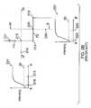
- FIGS. 1A-1BFor example, rectangles 101 on a mask, illustrated in FIG. 1A , are foreshortened into elliptical 102 on the resist, right angles are rounded, and the width of the shapes shrinks, as illustrated in FIG. 1B .
- the process of developing after exposing the wafer and the photoactive materiali.e. photoresist, equivalently referred to as resist
- the process of developing after exposing the wafer and the photoactive materiali.e. photoresist, equivalently referred to as resist
- resistalso adds to the uncertainty associated with the critical dimensions of the features.
- Other effects mainly related to the exposure and development effect associated with the resistexist that contribute to the distortions.
- the wafer shapesget deformed due the diffraction and scattering of light and other related optical and chemical effects of photo-resist materials.
- the combination of these lithographic processing effectsare known as optical proximity effects.
- OPCoptical proximity corrections
- MOPCmodel-based OPC
- MOPCmodel-based OPC
- RETresolution enhancement techniques
- altPSMalternating phase shift mask
- SRAFssub-resolution assist features
- CDcritical dimensions
- RET processesmay require heavy overexposure and large etch trim, which can pose a significant challenge to the OPC algorithm, since large discrepancies exist between mask size and actual on-wafer target size. For example, given an initial designed target CD on the mask, the final wafer polysilicon dimension may be shrunk by about 50%.
- the OPC algorithmcorrects the mask shapes based on simulated target shapes
- the fixed corrections applied to the mask shapesmay result in over-correction or under-correction which may converge to a solution only with difficulty, or may not converge at all.
- ACLVacross-chip line width variation
- model-based OPCdepends on a very accurate simulator that would predict the lithographic processing effects.
- the simulation of the image at points on the maskis computationally very expensive, and is typically limited to selected points.
- the simulatorpredicts the lithographic effect corresponding to selected points on the mask.
- a conventional OPC algorithmcompares the simulation to the target at the selected points, and if the difference exceeds a predefined threshold, the mask shape will be modified, typically by modifying the edge segments on the mask by a fixed amount. This process can be better understood by reference to FIGS. 2A-2F .
- FIG. 2Aillustrates a prior art target shape 307 that corresponds to the desired shape and size of the final pattern on the wafer.
- the corresponding mask shape 700initially is set equal to the target shape.
- the target shape 307is assumed to be a dark feature within the boundary of the shape 307 .
- the segmentation of the mask shape 700is shown in the expanded view 201 of a portion of the target and mask shape.
- a first segment F 1is defined by points 211 and 212 , and is connected to a second segment F 2 defined by points 212 and 213 .
- the OPC softwarewill typically segment the mask shape 700 and allow each segment to be moved independently in order to create the final corrected mask shape.
- cut A-A′is the simulation site across the first segment F 1 which intersects the segment at point 215 .
- Cut line B-B′is the simulation site along second segment F 2 , intersecting the segment F 2 at point 225 .
- a first step in creating the corrected mask shapeis to determine the initial error where the edge of each segment will be printed (based on a simulation) compared to where it is desired to be printed (based on the target layer 307 ).
- the mask shape 700is assumed to be equivalent to the desired target layer shape 307 and the edge placement error is computed along the simulation sites.
- the simulated image intensity along the simulation site A-A′is illustrated in the plot 251 , and the plot 252 illustrates the intensity along simulation site B-B′.
- the printed edge of the featureis the location where the image intensity crosses a threshold intensity 50 .
- the location along line A-A′ where the intensity crosses the threshold 50is indicated as 216 , and similarly, the location where the intensity crosses the threshold 50 is indicated as 226 .
- the printed edge 216 , 226 for both simulation sitesfall far inside the target edge 215 , 225 , respectively, for those sites. This indicates that the mask shape 700 for both segments F 1 , F 2 needs to be moved outward, or to the right for segment F 1 and up for segment F 2 . Since the printed edges 216 , 226 fall a large distance from the target edge 215 , 225 , respectively, the mask edge segments F 1 , F 2 are moved a large distance to try to compensate.
- the next step in creating the corrected mask shapeis to move the mask edge segments according to the computed errors and then resimulate the edge placements at the simulation sites.
- the mask edge segment F 2has moved outward past the location of simulation site A-A′.
- the resimulated image intensity along site A-A′is illustrated in the plot 251 ′ and along site B-B′ in the plot 252 ′.
- the computed edge 216 ′ for segment F 1now appears to move far beyond the edge target location 215 . This signifies to the OPC algorithm that segment F 1 needs to be moved inward or to the left.
- the edge 226 ′ for segment F 2is found to be converging on the target edge 225 .
- FIG. 2Dillustrates the mask edges 700 ′′ after the next iteration of moving segments F 1 and F 2 .
- a notch 705is beginning to appear at segment F 1 .
- the intensities at the simulation sites A-A′ (plot 251 ′′) and B-B′ (plot 252 ′′)are then resimulated and the edge placement errors computed.
- the edge 226 ′′ for segment F 2has now fully converged on the target edge 225 along simulation site B-B′.
- the placement of the mask edge along the segment F 2remains beyond simulation site A-A′ which is encompassed within the mask shape 700 ′′. Because of that, the printed edge 216 ′′ along simulation site A-A′ is still beyond the target edge 215 . This indicates to the OPC algorithm that the mask edge for segment F 1 still needs to be moved further to the left.
- the OPC algorithmwill move the segment F 1 again, as illustrated in FIG. 2E . Again the mask edge 700 ′′′ is moved and now a deep notch 705 ′ is visible at segment F 1 . Segment F 2 has not moved, as its edge 226 ′′′ has converged to the target edge 225 along simulation site B-B′ as illustrated in plot 252 ′′′. After simulation, the computed edge placement errors according to the OPC algorithm continue to indicate that, despite the large notch 705 ′ created at segment F 1 , the printed edge 216 ′′′ is still far beyond the target edge 215 . This is a consequence of the mask edge segment F 2 being placed beyond simulation site A-A′.
- the root cause of these errorslies in the large separation D in mask edge 700 ′′′ from target edge 307 .
- This separation Dcauses some simulation sites to be overrun by the mask edge, resulting in the simulation site not accurately predicting the behavior along the segment.
- MOPCmodel-based optical proximity correction
- the present inventionis directed to a method of designing a mask for forming a pattern on a wafer, the method including the steps of providing a process model describing a process for forming a pattern on a wafer, wherein the process includes the use of a mask; decomposing the process model into a pattern dependent model process and a constant term; providing a desired wafer target pattern; biasing the desired wafer target pattern with the constant term to form a simulation target pattern; providing an initial mask design; and modifying the initial mask design to form a final mask design, so that when the final mask is used as the mask in the pattern dependent model process, a simulated wafer pattern is obtained that matches the simulation target pattern within an acceptance criterion.
- the inventionprovides for modifying the target design used in the MBOPC algorithm by a constant bias from the decomposed process model, and the modified target design is then the target that the MBOPC uses to determine when the sufficiency of mask correction is achieved.
- the inventionprovides that the simulation is performed using the decomposed pattern dependent portion of the process model.
- the inventive mask design processis applicable to multiple process models including a lithographic image model, a resist model, an etch model or a combination thereof.
- a modelmay be provided for each subprocess, and each subprocess model is individually decomposed into a pattern dependent process model and a constant term.
- the bias applied to the target designincludes the constant terms from each of the decomposed subprocess models, and the simulation is performed using the decomposed pattern dependent models, according to the sequence of the subprocesses.
- FIG. 1A-1Billustrates a pattern on a mask ( 1 A) and the corresponding pattern of the wafer resist image ( 1 B) as simulated an optical and resist model used in OPC.
- FIGS. 2A-2Fillustrate steps of a conventional OPC procedure wherein corrections to the mask are made by adjusting segment positions.
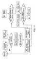
- FIG. 3illustrates a flow diagram of method steps of a conventional OPC algorithm.
- FIG. 4illustrates a flow diagram of method steps of a conventional OPC algorithm including optical rule checking (ORC) of the mask design.
- ORCoptical rule checking
- FIG. 5illustrates a flow chart of an embodiment of an OPC process according to the present invention.
- FIG. 6illustrates typical variations in feature dimensions as a function of pattern spacing (pitch) across a wafer.
- FIG. 7illustrates a decomposition of variations in feature dimensions into a pattern dependent and constant terms.
- FIG. 8illustrates a flow chart of an embodiment of an OPC process including ORC according to the present invention.
- FIG. 9Aillustrates a prior art adjusted target used for OPC overlain for comparison with an target adjusted in accordance with the present invention.
- FIG. 9Billustrates a mask design resulting from OPC using a prior art adjusted target.
- FIG. 9Cillustrates a mask design resulting from OPC using a target adjusted in accordance with the invention.
- FIG. 10plots edge placement error (EPE) distributions obtained using prior art OPC models compared to EPE distributions obtained when performing OPC according to the present invention.
- EPEedge placement error
- FIG. 11illustrates a flow chart for an embodiment of the present invention using multiple process models.
- Model Build 60a model based optical proximity correction
- Data Prep 30the use of that model to create a photomask design based on the design of the semiconductor integrated circuit to be formed on a wafer.
- the model build process 60is generally carried out one time for each semiconductor printing process that is used in the overall semiconductor manufacturing process.
- the data prep process 30is repeated on every semiconductor design that will be run through the semiconductor manufacturing process. In a typical semiconductor foundry business, there may be hundreds of different designs that will be run through the same data prep process.
- Model Build 60typically requires that process data (Block 301 ) be collected that represents the manufacturing process that will be used to print patterns on the wafer.
- the process data collectedis based on a set of test patterns (Block 302 ) that represent typical types of patterns that will exist in semiconductor designs that will be built using the manufacturing process.
- a process modeldescribes the relationship between the process data and the test pattern designs that were used to create the process data.
- the modelis calibrated (Block 303 ) by fitting this relationship to predetermined model forms. This can be accomplished using various numerical techniques.
- the result of the calibration step 303is an OPC model, or process model ( 304 ), that provides a mathematical means to describe the changes introduced when an ideal photomask pattern is transferred onto a wafer through a printing process.
- the data preparation step (Data Prep 30 ) of a MBOPC flowis also well known in the art.
- a desired target to be printed on the wafer 307is provided as input.
- the initial wafer target 307is derived from the design for a specific semiconductor chip or IC.
- the IC designis also typically used as a starting point for deriving the initial mask shape that will be corrected by the MBOPC process, and is also provided as input (Block 307 ).
- Block 307Generally, single layers of the design are processed individually and that is the process that is described in this example. It is understood that multiple layers could be processed simultaneously.
- a biasis typically applied to the design shapes on the wafer target so that the shape sizes will be equivalent to the final dimensions that are desired on the semiconductor wafer.
- the MBOPC softwaredetermines corrections that will be applied to the initial mask design to ensure that the printed result approximates the wafer target ( 307 ).
- a set of control parameters ( 308 )are used to control the movement of the mask edges and these control parameters also impact the corrections that are applied to the mask design.
- This correction step 309is generally called model based optical proximity correction (MBOPC), although it is understood that many more effects, in addition to optical proximity effects, may typically be corrected through the MBOPC process.
- a mask design ( 310 )that may or may not look similar to the IC design, but should result in a final wafer pattern that looks similar to the wafer target ( 307 ), at least in terms of the desired critical dimensions (CDs).
- FIG. 4is a straightforward extension of FIG. 3 , showing the addition of a results checking step 401 that is performed on the final mask design 310 .
- the model build process 60(comprising Blocks 301 - 304 ) is the same as shown in FIG. 3 .
- the Data Prep process 31includes the same data prep process (Blocks 307 - 310 ) as in FIG. 3 , and delivers the same final mask design 310 for each semiconductor IC layer design. However, in this example, Data Prep 31 includes the additional step of checking (Block 401 ) the mask design 310 to ensure that the design 310 resulting from the MBOPC was correct, within a set of design rules.
- This design check step (Block 401 )is often called optical rules checking, or ORC, and entails applying the process model ( 304 ) to the mask design ( 310 ) and obtaining (e.g. simulating or computing) contours that represent the final wafer shapes that will be printed.
- the process model 304may include the optical image, the resist image process as well as the etch process. These contours are then compared to the wafer target ( 307 ) and checked to make sure they satisfy various rules such as manufacturability rules. The results of these checks ( 402 ) are used to determine whether the MBOPC process was successful and whether the mask 310 should be built.
- FIG. 5is a flowchart representing the preferred embodiment of the invention.
- the inventive MBOPC processis divided into 2 main sections: Model Build 61 , comprising Blocks 301 - 304 and additional Blocks 701 - 703 ; and Data Prep 70 , comprising Blocks 307 and 704 - 708 .
- the process modelis calibrated in a manner similar to the conventional Model Build process flow 60 , to result in a process model 304 .
- an additional stepis taken to decompose the model (Block 701 ) into two components.
- the first model componentis a constant term that 702 is independent of pattern type.
- this global bias term 702has a negative value, meaning that the patterns are made globally smaller during the Data Prep section 70 , to be discussed below.
- the second model componentis a pattern dependent portion of the process model or component 703 (which may comprise one or more terms or functions) that describes the non-constant relationship between the mask patterns and the final wafer patterns. Together, the constant term ( 702 ) and the pattern dependent process model portion ( 703 ) add up to make the process model ( 304 ).
- FIG. 6is a plot of variations in critical dimension (CD) as a function of across-chip pattern variations, specifically over the range of pitches of various patterns in the IC layer.
- FIG. 6illustrates an example of across-chip CD or line-width variation after development of the resist (curve 501 ) and after etch (curve 503 ). Both the after-develop CD curve 501 and the final CD (after etch) curve 503 show very similar behavior, suggesting that the etch process line-width variation 503 follows the line-width variation trend 501 introduced by the resist process.
- FIG. 7illustrates a plot of a net etch process variation 504 through pitch, illustrating how the etch process model 304 can be decomposed into a constant offset 702 plus a non-linear pattern-dependent component 703 during modeling, in accordance with the present invention.
- the Data Prep 70 section of the preferred embodimentcomprises a wafer target 307 and initial mask design (e.g. based on the chip or IC design) that is the input to this flow (similar to the prior flows of FIGS. 3 and 4 ) and this flow is repeated for all chip or IC designs that will be run through the specified manufacturing process.
- initial mask designe.g. based on the chip or IC design
- the formation of the inventive target layer 705includes biasing the wafer target 307 with the constant term 702 to obtain a simulation wafer target 705 which will be used by the MBOPC algorithm to evaluate the results of the simulated wafer pattern resulting from the mask design, rather than comparing the simulated wafer pattern to the desired wafer target 307 , as in the conventional method.
- the biasing of the wafer target 307 with the constant term 702will typically result in shapes on the simulation wafer target 705 that are larger than the corresponding shapes on the desired wafer target 307 in the conventional process, as illustrated in FIG. 9A .
- the mask layer(which initially is typically set equal to the design layer) is then modified by the MBOPC software in the MBOPC (Block 707 ) until the simulated wafer pattern (which could be any pattern such as an image or an etched pattern) matches the simulation target 705 within an acceptance criterion.
- the pattern dependent component 703 of the process model 304are used as the simulation process model in MBOPC and the control parameters 706 for the corrections are likely to be different than those used in the conventional flow.
- the output of the MBOPC step 707is a corrected mask design 708 where the corrections applied may be different than those applied in the prior art process.
- FIG. 9Cillustrates the improvement in the final mask design 708 compared to the simulation target dimensions 705 .
- the target dimensions 705are larger than the final etch target by an amount equal to the constant bias 702 .
- cornersare less of a problem compared to prior art methods, since the simulation sites are placed closer to the final mask dimension.
- the resulting mask 310may have a narrow notch of dimension 319 .
- the final mask 708has a contour, for example width 719 near the corner, that more closely conforms to the shape of the simulation target 705 , as illustrated in FIG. 9C .
- FIG. 8A second embodiment of the invention is shown in FIG. 8 .
- This caseis nearly identical with the embodiment illustrated in FIG. 5 , except that a results checking step 801 is performed on the final mask design 708 in the Data Prep section 71 .
- the ORC step 801has been included into the preferred embodiment of the invention.
- the ORC step 801applies the pattern dependent component of the model 703 to the mask design 708 .
- the resulting contoursare compared to the simulation target 705 and checked to make sure they satisfy the design and manufacturability rules. Again, the results of these checks 802 are used to determine whether the MBOPC process was successful and whether the mask should be built.
- FIG. 10illustrates the improved across chip line-width variation (ACLV) obtained when MBOPC is performed in accordance with the present invention.
- the edge placement error distributions (EPE) at all edges 1010 and at gate edges 1011 for the prior art MBOPCwere compared to EPE at all edges 1020 and at gate edges 1021 using MBOPC according to the present invention.
- the 3 ⁇ EPE distributionis improved for gate edges and all edges when the MBOPC of the present invention is used.
- a process model 904 ( i ) for a given step i in the overall processis calibrated using process data 901 ( i ) taken after that process step i has been completed.
- the model 904 ( i )is calibrated (Block 903 ) resulting in a calibrated process model 904 ( i ) for the given process step i.
- This process model 904 ( i )is then decomposed (Block 905 ) into a constant term 906 ( i ) and a pattern dependent process model portion or component 907 ( i ) for the process step i.
- This calibration procedurecan be repeated ( 908 ) for each step i of n processes that need to be modeled.
- the difference between these methodsis represented by the dotted arrow ( 909 ) that flows into the calibration step 903 for a given process i that depends on the results of the decomposed process model 906 ( i ⁇ 1), 907 ( i ⁇ 1) of the previous process i ⁇ 1.
- this arrowshould not exist and each process model i can be built without knowledge of the previous process model i ⁇ 1.
- the more typical situationis where a given process is dependent on a previous process step and the data collected for that process has also passed through the previous process step.
- the arrow ( 909 )is required, as the calibration step for the current process i must use the previous step's model (i ⁇ 1) in order to pre-process the test patterns ( 902 ) before calibrating for the current step i.
- the etch processshould be modeled as the transformation of the post-lithography photoresist pattern to a final etched pattern. It should not be modeled as the transformation of a photomask pattern to a final etch pattern. So, the lithography process model must be known in order to build the etch model based on the etch data and the designed test patterns.
- the data prep flowis very similar to the data prep flow 70 of FIG. 5 .
- the constant term 906is now the sum of all of the individual constant terms for all of the process models i through n.
- the resulting simulation target ( 911 ) and the control parameters ( 912 )are then input into the MBOPC step ( 913 ).
- the MBOPC step 913may apply the models in various ways, but the most common method would be to apply each model in succession to the design data. The order of the succession would match the order of the process steps that are being modeled.
- the pattern dependent portion 907 ( i ) of a given process model 904 ( i )will operate on the combination of the pattern dependent component and constant term of the previous model (i ⁇ 1).
Landscapes
- Physics & Mathematics (AREA)
- General Physics & Mathematics (AREA)
- Preparing Plates And Mask In Photomechanical Process (AREA)
- Exposure And Positioning Against Photoresist Photosensitive Materials (AREA)
Abstract
Description
- The present invention relates in general to semiconductor integrated circuit (IC) process technology, particularly, photolithography used in fabrication of semiconductor ICs, and more particularly to optical proximity correction.
- The advent of advanced lithographic techniques and the attempt of chip manufacturers to closely follow Moore's law predicting an exponential growth of number of components on a chip and their shrinkage on the wafer is making the process of designing tools for automating the chip design extremely challenging. The chip is imprinted by means of optical lithographic techniques on the silicon wafer by way of chrome on glassmasks. As the components on the chip become smaller, they are now in the verge of reaching the limits of capacity of the lithographic process.
- One of the most common problem of printing integrated circuits on silicon wafers from the mask using lithographic processing is the loss of fidelity of the mask shapes. The dimensions of the wafer shapes are usually much smaller than the wavelength of light that is used in the lithographic processing. The non-linearities associated with this lithographic process of imprinting and the laws of physics associated with light (including diffraction of light waves) makes impressing highly unpredictable. Referring to
FIGS. 1A-1B , for example,rectangles 101 on a mask, illustrated inFIG. 1A , are foreshortened into elliptical102 on the resist, right angles are rounded, and the width of the shapes shrinks, as illustrated inFIG. 1B . In addition to the non-linearity associated with the optical effects, the process of developing after exposing the wafer and the photoactive material (i.e. photoresist, equivalently referred to as resist) thereon also adds to the uncertainty associated with the critical dimensions of the features. Other effects mainly related to the exposure and development effect associated with the resist exist that contribute to the distortions. The wafer shapes get deformed due the diffraction and scattering of light and other related optical and chemical effects of photo-resist materials. The combination of these lithographic processing effects are known as optical proximity effects. - To counter the problem of optical proximity, and increase the fidelity of the wafer printing, mask designers take into account the deformities introduced by the aforementioned lithographic processing effects by intentionally and systematically distorting the original shapes on the mask. The net result of these distortions is that the imprinted shape on the wafer ultimately looks like the target or intended images, satisfying the design rules that were created to achieve the desired yield in chip manufacturing. These methods are generally referred to as optical proximity corrections (OPC). OPC may be performed by simulating the imaging and on-wafer processes, such as etch processes, comparing the simulated image to the target image, and adjusting the mask design so that the simulated image will more closely resemble the target image. This method, also known as model-based OPC (MBOPC), emulates the physical and optical effects that are mostly responsible for shape deformations. At the heart of these methods is a computer simulation program that, given the appropriate optical and physical parameters and the original dimension of the object on the mask, predicts, with a certain degree of accuracy, the printed dimension of the object on the wafer. In the correction phase of the model-based optical proximity correction (MBOPC), the shape on the mask is iteratively modified so that the resulting output closely approximates, within an acceptance criterion, what is desired for the image or imprinted shape on the wafer. This method automatically deforms existing mask shapes to achieve the target dimensions on the wafer.
- As target feature size continues to shrink, resolution enhancement techniques (RET) such as alternating phase shift mask (altPSM) or sub-resolution assist features (SRAFs) may be used to print the desired critical dimensions (CD) and provide sufficient lithographic process latitude. RET processes may require heavy overexposure and large etch trim, which can pose a significant challenge to the OPC algorithm, since large discrepancies exist between mask size and actual on-wafer target size. For example, given an initial designed target CD on the mask, the final wafer polysilicon dimension may be shrunk by about 50%. Since the OPC algorithm corrects the mask shapes based on simulated target shapes, the fixed corrections applied to the mask shapes may result in over-correction or under-correction which may converge to a solution only with difficulty, or may not converge at all. In addition, even if a solution is found, there may be large across-chip line width variation (ACLV), and in particular, problems in controlling the gate and polysilicon line widths.
- The success of model-based OPC depends on a very accurate simulator that would predict the lithographic processing effects. The simulation of the image at points on the mask is computationally very expensive, and is typically limited to selected points. The simulator predicts the lithographic effect corresponding to selected points on the mask. A conventional OPC algorithm compares the simulation to the target at the selected points, and if the difference exceeds a predefined threshold, the mask shape will be modified, typically by modifying the edge segments on the mask by a fixed amount. This process can be better understood by reference to
FIGS. 2A-2F . - For example,
FIG. 2A illustrates a priorart target shape 307 that corresponds to the desired shape and size of the final pattern on the wafer. Thecorresponding mask shape 700 initially is set equal to the target shape. In this example, thetarget shape 307 is assumed to be a dark feature within the boundary of theshape 307. In the expandedview 201 of a portion of the target and mask shape, the segmentation of themask shape 700 is shown. A first segment F1 is defined bypoints points mask shape 700 and allow each segment to be moved independently in order to create the final corrected mask shape. To determine how to move each segment, the lithography process is simulated along a single cut across the segment. These cuts are called the simulation sites. Here, cut A-A′ is the simulation site across the first segment F1 which intersects the segment atpoint 215. Cut line B-B′ is the simulation site along second segment F2, intersecting the segment F2 atpoint 225. By only simulating along a single simulation site per segment, the OPC software is able to simulate the lithography behavior across an entire chip in a reasonable amount of time. - Referring to
FIG. 2B , a first step in creating the corrected mask shape is to determine the initial error where the edge of each segment will be printed (based on a simulation) compared to where it is desired to be printed (based on the target layer307). Initially, themask shape 700 is assumed to be equivalent to the desiredtarget layer shape 307 and the edge placement error is computed along the simulation sites. The simulated image intensity along the simulation site A-A′ is illustrated in theplot 251, and theplot 252 illustrates the intensity along simulation site B-B′. The printed edge of the feature is the location where the image intensity crosses athreshold intensity 50. The location along line A-A′ where the intensity crosses thethreshold 50 is indicated as216, and similarly, the location where the intensity crosses thethreshold 50 is indicated as226. Initially, the printededge target edge mask shape 700 for both segments F1, F2 needs to be moved outward, or to the right for segment F1 and up for segment F2. Since theprinted edges target edge - The next step in creating the corrected mask shape is to move the mask edge segments according to the computed errors and then resimulate the edge placements at the simulation sites. Referring to
FIG. 2C , the mask edge segment F2 has moved outward past the location of simulation site A-A′. The resimulated image intensity along site A-A′ is illustrated in theplot 251′ and along site B-B′ in theplot 252′. It can be seen that the computededge 216′ for segment F1 now appears to move far beyond theedge target location 215. This signifies to the OPC algorithm that segment F1 needs to be moved inward or to the left. On the other hand, theedge 226′ for segment F2 is found to be converging on thetarget edge 225. FIG. 2D illustrates themask edges 700″ after the next iteration of moving segments F1 and F2. Anotch 705 is beginning to appear at segment F1. The intensities at the simulation sites A-A′ (plot 251″) and B-B′ (plot 252″) are then resimulated and the edge placement errors computed. Theedge 226″ for segment F2 has now fully converged on thetarget edge 225 along simulation site B-B′. However, the placement of the mask edge along the segment F2 remains beyond simulation site A-A′ which is encompassed within themask shape 700″. Because of that, the printededge 216″ along simulation site A-A′ is still beyond thetarget edge 215. This indicates to the OPC algorithm that the mask edge for segment F1 still needs to be moved further to the left.- Thus, the OPC algorithm will move the segment F1 again, as illustrated in
FIG. 2E . Again themask edge 700′″ is moved and now adeep notch 705′ is visible at segment F1. Segment F2 has not moved, as itsedge 226′″ has converged to thetarget edge 225 along simulation site B-B′ as illustrated inplot 252′″. After simulation, the computed edge placement errors according to the OPC algorithm continue to indicate that, despite thelarge notch 705′ created at segment F1, the printededge 216′″ is still far beyond thetarget edge 215. This is a consequence of the mask edge segment F2 being placed beyond simulation site A-A′. - This iterative process will continue without any real progress in reducing the edge placement error at site A-A′. At some point, the OPC software will give up trying to fix this point and will leave the
large notch 705″ in place, as inFIG. 2F . The main problem with this solution is that thelarge notch 705″ at segment F1 can cause a very narrow feature to be printed. By comparing the simulated contour along a cut C-C′ (that was not used for the OPC correction) to the simulated contour along the site A-A′ that was used for the OPC correction, it is apparent that the printededge 216′″ may fall deep inside thetarget edge 215, causing a risk of failure. Asimulated contour 250 shows the ringing that can occur close to the notch. - The root cause of these errors lies in the large separation D in
mask edge 700′″ fromtarget edge 307. This separation D causes some simulation sites to be overrun by the mask edge, resulting in the simulation site not accurately predicting the behavior along the segment. - There is, therefore, a need for a method that can improve the robustness of the OPC correction algorithm, that can improve the OPC algorithm for RET methods such as over exposure and etch trim, and to provide improvements to lithography process robustness and improve ACLV.
- It is therefore an objective of the present invention to provide a method and system for designing masks, for example, by performing model-based optical proximity correction (MBOPC), that improves across-chip line-width variations.
- It is a further objective of the present invention to provide an MBOPC method and system that is compatible with existing MBOPC software.
- It is yet a further objective of the present invention to provide an MBOPC method and system that is robust and will converge to a final mask design that minimizes defects.
- It is still a further objective of the present invention to provide an mask design method, such as MBOPC method and system, that can incorporate multiple processes.
- Accordingly, the present invention is directed to a method of designing a mask for forming a pattern on a wafer, the method including the steps of providing a process model describing a process for forming a pattern on a wafer, wherein the process includes the use of a mask; decomposing the process model into a pattern dependent model process and a constant term; providing a desired wafer target pattern; biasing the desired wafer target pattern with the constant term to form a simulation target pattern; providing an initial mask design; and modifying the initial mask design to form a final mask design, so that when the final mask is used as the mask in the pattern dependent model process, a simulated wafer pattern is obtained that matches the simulation target pattern within an acceptance criterion.
- Stated another way, the invention provides for modifying the target design used in the MBOPC algorithm by a constant bias from the decomposed process model, and the modified target design is then the target that the MBOPC uses to determine when the sufficiency of mask correction is achieved. However, the invention provides that the simulation is performed using the decomposed pattern dependent portion of the process model.
- The inventive mask design process is applicable to multiple process models including a lithographic image model, a resist model, an etch model or a combination thereof. In the case where the process includes a plurality of subprocesses, a model may be provided for each subprocess, and each subprocess model is individually decomposed into a pattern dependent process model and a constant term. The bias applied to the target design includes the constant terms from each of the decomposed subprocess models, and the simulation is performed using the decomposed pattern dependent models, according to the sequence of the subprocesses.
- The foregoing has outlined rather broadly the features and technical advantages of the present invention in order that the detailed description of the invention that follows may be better understood. Additional features and advantages of the invention will be described hereinafter which form the subject of the claims of the invention.
- For a more complete understanding of the present invention, and the advantages thereof, reference is now made to the following descriptions taken in conjunction with the accompanying drawings, which are not necessarily drawn to scale.
FIG. 1A-1B illustrates a pattern on a mask (1A) and the corresponding pattern of the wafer resist image (1B) as simulated an optical and resist model used in OPC.FIGS. 2A-2F illustrate steps of a conventional OPC procedure wherein corrections to the mask are made by adjusting segment positions.FIG. 3 illustrates a flow diagram of method steps of a conventional OPC algorithm.FIG. 4 illustrates a flow diagram of method steps of a conventional OPC algorithm including optical rule checking (ORC) of the mask design.FIG. 5 illustrates a flow chart of an embodiment of an OPC process according to the present invention.FIG. 6 illustrates typical variations in feature dimensions as a function of pattern spacing (pitch) across a wafer.FIG. 7 illustrates a decomposition of variations in feature dimensions into a pattern dependent and constant terms.FIG. 8 illustrates a flow chart of an embodiment of an OPC process including ORC according to the present invention.FIG. 9A illustrates a prior art adjusted target used for OPC overlain for comparison with an target adjusted in accordance with the present invention.FIG. 9B illustrates a mask design resulting from OPC using a prior art adjusted target.FIG. 9C illustrates a mask design resulting from OPC using a target adjusted in accordance with the invention.FIG. 10 plots edge placement error (EPE) distributions obtained using prior art OPC models compared to EPE distributions obtained when performing OPC according to the present invention.FIG. 11 illustrates a flow chart for an embodiment of the present invention using multiple process models.- In the following description, numerous specific details may be set forth to provide a thorough understanding of the present invention. However, it will be obvious to those skilled in the art that the present invention may be practiced without such specific details.
- Refer now to the drawings wherein depicted elements are not necessarily shown to scale and wherein like or similar elements are designated by the same reference numeral through the several views.
- Referring to
FIG. 3 , a flow diagram of a conventional model based optical proximity correction (MBOPC) process is illustrated. The MBOPC process consists of two major sections: the creation of a model, referred to asModel Build 60, including Blocks301-304, and the use of that model to create a photomask design based on the design of the semiconductor integrated circuit to be formed on a wafer, referred to asData Prep 30, including Blocks307-310. Themodel build process 60 is generally carried out one time for each semiconductor printing process that is used in the overall semiconductor manufacturing process. On the other hand, thedata prep process 30 is repeated on every semiconductor design that will be run through the semiconductor manufacturing process. In a typical semiconductor foundry business, there may be hundreds of different designs that will be run through the same data prep process. - Building OPC models (Model Build60) is well known in the art and only an overview will be described here to aid in understanding the present invention.
Model Build 60 typically requires that process data (Block301) be collected that represents the manufacturing process that will be used to print patterns on the wafer. The process data collected is based on a set of test patterns (Block302) that represent typical types of patterns that will exist in semiconductor designs that will be built using the manufacturing process. A process model describes the relationship between the process data and the test pattern designs that were used to create the process data. The model is calibrated (Block303) by fitting this relationship to predetermined model forms. This can be accomplished using various numerical techniques. The result of thecalibration step 303 is an OPC model, or process model (304), that provides a mathematical means to describe the changes introduced when an ideal photomask pattern is transferred onto a wafer through a printing process. - The data preparation step (Data Prep30) of a MBOPC flow is also well known in the art. A desired target to be printed on the
wafer 307 is provided as input. In a typical example, theinitial wafer target 307 is derived from the design for a specific semiconductor chip or IC. The IC design is also typically used as a starting point for deriving the initial mask shape that will be corrected by the MBOPC process, and is also provided as input (Block307). Generally, single layers of the design are processed individually and that is the process that is described in this example. It is understood that multiple layers could be processed simultaneously. A bias is typically applied to the design shapes on the wafer target so that the shape sizes will be equivalent to the final dimensions that are desired on the semiconductor wafer. This creates a wafer target layer (Block307) that will be used by the MBOPC software as the desired result. For example, if a CD of 87 nm is specified in the IC design, and the desired target CD is 42 nm, then a bias of 45 nm may be applied to the IC design to form thewafer target layer 307 as input to the MBOPC. - Using the
process model 304 created previously, the MBOPC software then determines corrections that will be applied to the initial mask design to ensure that the printed result approximates the wafer target (307). A set of control parameters (308) are used to control the movement of the mask edges and these control parameters also impact the corrections that are applied to the mask design. Thiscorrection step 309 is generally called model based optical proximity correction (MBOPC), although it is understood that many more effects, in addition to optical proximity effects, may typically be corrected through the MBOPC process. The end result of this is a mask design (310) that may or may not look similar to the IC design, but should result in a final wafer pattern that looks similar to the wafer target (307), at least in terms of the desired critical dimensions (CDs). FIG. 4 is a straightforward extension ofFIG. 3 , showing the addition of aresults checking step 401 that is performed on thefinal mask design 310. In this case, the model build process60 (comprising Blocks301-304) is the same as shown inFIG. 3 . TheData Prep process 31 includes the same data prep process (Blocks307-310) as inFIG. 3 , and delivers the samefinal mask design 310 for each semiconductor IC layer design. However, in this example,Data Prep 31 includes the additional step of checking (Block401) themask design 310 to ensure that thedesign 310 resulting from the MBOPC was correct, within a set of design rules. This design check step (Block401) is often called optical rules checking, or ORC, and entails applying the process model (304) to the mask design (310) and obtaining (e.g. simulating or computing) contours that represent the final wafer shapes that will be printed. As discussed above, theprocess model 304 may include the optical image, the resist image process as well as the etch process. These contours are then compared to the wafer target (307) and checked to make sure they satisfy various rules such as manufacturability rules. The results of these checks (402) are used to determine whether the MBOPC process was successful and whether themask 310 should be built.FIG. 5 is a flowchart representing the preferred embodiment of the invention. As inFIG. 3 , the inventive MBOPC process is divided into 2 main sections:Model Build 61, comprising Blocks301-304 and additional Blocks701-703; andData Prep 70, comprisingBlocks 307 and704-708. In accordance with the present invention, the process model is calibrated in a manner similar to the conventional ModelBuild process flow 60, to result in aprocess model 304. At this point, an additional step is taken to decompose the model (Block701) into two components. The first model component is a constant term that702 is independent of pattern type. Typically, thisglobal bias term 702 has a negative value, meaning that the patterns are made globally smaller during theData Prep section 70, to be discussed below. The second model component is a pattern dependent portion of the process model or component703 (which may comprise one or more terms or functions) that describes the non-constant relationship between the mask patterns and the final wafer patterns. Together, the constant term (702) and the pattern dependent process model portion (703) add up to make the process model (304).- The decomposition (Block701) of the
process model 304 intoconstant term 702 and pattern dependentprocess model portion 703 is illustrated by reference toFIGS. 6 and 7 .FIG. 6 is a plot of variations in critical dimension (CD) as a function of across-chip pattern variations, specifically over the range of pitches of various patterns in the IC layer.FIG. 6 illustrates an example of across-chip CD or line-width variation after development of the resist (curve501) and after etch (curve503). Both the after-develop CD curve 501 and the final CD (after etch)curve 503 show very similar behavior, suggesting that the etch process line-width variation 503 follows the line-width variation trend 501 introduced by the resist process. FIG. 7 illustrates a plot of a netetch process variation 504 through pitch, illustrating how theetch process model 304 can be decomposed into a constant offset702 plus a non-linear pattern-dependent component 703 during modeling, in accordance with the present invention.- Referring again to
FIG. 5 , theData Prep 70 section of the preferred embodiment comprises awafer target 307 and initial mask design (e.g. based on the chip or IC design) that is the input to this flow (similar to the prior flows ofFIGS. 3 and 4 ) and this flow is repeated for all chip or IC designs that will be run through the specified manufacturing process. In accordance with the present invention, the formation of the inventive target layer705 (Block704) includes biasing thewafer target 307 with theconstant term 702 to obtain asimulation wafer target 705 which will be used by the MBOPC algorithm to evaluate the results of the simulated wafer pattern resulting from the mask design, rather than comparing the simulated wafer pattern to the desiredwafer target 307, as in the conventional method. The biasing of thewafer target 307 with theconstant term 702 will typically result in shapes on thesimulation wafer target 705 that are larger than the corresponding shapes on the desiredwafer target 307 in the conventional process, as illustrated inFIG. 9A . In a similar manner to the prior art method, the mask layer (which initially is typically set equal to the design layer) is then modified by the MBOPC software in the MBOPC (Block707) until the simulated wafer pattern (which could be any pattern such as an image or an etched pattern) matches thesimulation target 705 within an acceptance criterion. In this case, however, only the patterndependent component 703 of theprocess model 304 are used as the simulation process model in MBOPC and thecontrol parameters 706 for the corrections are likely to be different than those used in the conventional flow. The output of theMBOPC step 707 is a correctedmask design 708 where the corrections applied may be different than those applied in the prior art process. FIG. 9C illustrates the improvement in thefinal mask design 708 compared to thesimulation target dimensions 705. In this case, thetarget dimensions 705 are larger than the final etch target by an amount equal to theconstant bias 702. In this case, corners are less of a problem compared to prior art methods, since the simulation sites are placed closer to the final mask dimension. For example, referring toFIG. 9B , in a conventional MBOPC method, the resultingmask 310 may have a narrow notch ofdimension 319. However, thefinal mask 708 has a contour, for example width719 near the corner, that more closely conforms to the shape of thesimulation target 705, as illustrated inFIG. 9C .- A second embodiment of the invention is shown in
FIG. 8 . This case is nearly identical with the embodiment illustrated inFIG. 5 , except that aresults checking step 801 is performed on thefinal mask design 708 in the Data Prep section71. In a manner analogous to the addition of an ORC step into the standard OPC flow (seeFIG. 4 ), theORC step 801 has been included into the preferred embodiment of the invention. Here theORC step 801 applies the pattern dependent component of themodel 703 to themask design 708. The resulting contours are compared to thesimulation target 705 and checked to make sure they satisfy the design and manufacturability rules. Again, the results of thesechecks 802 are used to determine whether the MBOPC process was successful and whether the mask should be built. FIG. 10 illustrates the improved across chip line-width variation (ACLV) obtained when MBOPC is performed in accordance with the present invention. The edge placement error distributions (EPE) at alledges 1010 and atgate edges 1011 for the prior art MBOPC were compared to EPE at alledges 1020 and atgate edges 1021 using MBOPC according to the present invention. The 3σ EPE distribution is improved for gate edges and all edges when the MBOPC of the present invention is used.- Other embodiments of the present invention are possible. For example, referring to
FIG. 11 , multiple process steps may be accounted for by using separate process models or subprocesses. For example, the separate process models could include, but are not limited to, a mask process model, a lithographic image model, a resist model, an etch model, a chemical-mechanical polishing (CMP) process model or a combination thereof. In this case, a process model904(i) for a given step i in the overall process is calibrated using process data901(i) taken after that process step i has been completed. Using this data and the test pattern designs902, the model904(i) is calibrated (Block903) resulting in a calibrated process model904(i) for the given process step i. This process model904(i) is then decomposed (Block905) into a constant term906(i) and a pattern dependent process model portion or component907(i) for the process step i. This calibration procedure can be repeated (908) for each step i of n processes that need to be modeled. Here there are two slightly different methods that can be used, depending on the process being modeled and how the data is collected. The difference between these methods is represented by the dotted arrow (909) that flows into thecalibration step 903 for a given process i that depends on the results of the decomposed process model906(i−1),907(i−1) of the previous process i−1. In the case where data for a given process can be collected completely independently from the other processes being modeled, then this arrow should not exist and each process model i can be built without knowledge of the previous process model i−1. However, the more typical situation is where a given process is dependent on a previous process step and the data collected for that process has also passed through the previous process step. In this case, the arrow (909) is required, as the calibration step for the current process i must use the previous step's model (i−1) in order to pre-process the test patterns (902) before calibrating for the current step i. For example, to model an etch process following a lithography process, the etch process should be modeled as the transformation of the post-lithography photoresist pattern to a final etched pattern. It should not be modeled as the transformation of a photomask pattern to a final etch pattern. So, the lithography process model must be known in order to build the etch model based on the etch data and the designed test patterns. - In this embodiment, the data prep flow is very similar to the
data prep flow 70 ofFIG. 5 . The desiredwafer target 307 is again biased (Block910) to asimulation target 911 by the constant portions of the process model (906, i=1, . . . , n). In this case, theconstant term 906 is now the sum of all of the individual constant terms for all of the process models i through n. The resulting simulation target (911) and the control parameters (912) are then input into the MBOPC step (913). This step will then apply the pattern dependent components907(i), i=1, . . . , n of the various process models to create the correctedmask design 914. TheMBOPC step 913 may apply the models in various ways, but the most common method would be to apply each model in succession to the design data. The order of the succession would match the order of the process steps that are being modeled. - It is recognized that because of the sequential processing of the models, that the pattern dependent portion907(i) of a given process model904(i) will operate on the combination of the pattern dependent component and constant term of the previous model (i−1). For example, when modeling a lithography process, the lithographically patterned dimension of a feature may be represented as D′=PL(D)+CL, where D′ is the post-lithography dimension of the feature, D is the pre-lithography (mask) dimension of the feature, PL is the pattern dependent lithography model portion and CL is the constant term of the lithography model. If the lithography process is then followed by an etch process, the post-etch dimension for the same pattern will be given by D″=PE(D′)+CE, where D″ is the post-etch dimension, D′ is the post-lithography dimension, PE is the pattern dependent etch model and CE is the constant term of the etch model. So, the final dimension can be found from the mask dimension using D″=PE(PL(D)+CL)+CE, which indicates that the pattern dependent etch model is applied to the true post-lithography pattern, not just the pattern dependent process model component.
- Although the present invention and its advantages have been described in detail, it should be understood that various changes, substitutions and alterations can be made herein without departing from the spirit and scope of the invention as defined by the appended claims.
Claims (31)
Priority Applications (2)
| Application Number | Priority Date | Filing Date | Title |
|---|---|---|---|
| US10/904,355US7350183B2 (en) | 2004-11-05 | 2004-11-05 | Method for improving optical proximity correction |
| CNB2005101175593ACN100465971C (en) | 2004-11-05 | 2005-11-04 | Method for improving optical proximity correction |
Applications Claiming Priority (1)
| Application Number | Priority Date | Filing Date | Title |
|---|---|---|---|
| US10/904,355US7350183B2 (en) | 2004-11-05 | 2004-11-05 | Method for improving optical proximity correction |
Publications (2)
| Publication Number | Publication Date |
|---|---|
| US20060101370A1true US20060101370A1 (en) | 2006-05-11 |
| US7350183B2 US7350183B2 (en) | 2008-03-25 |
Family
ID=36317792
Family Applications (1)
| Application Number | Title | Priority Date | Filing Date |
|---|---|---|---|
| US10/904,355Active2025-12-10US7350183B2 (en) | 2004-11-05 | 2004-11-05 | Method for improving optical proximity correction |
Country Status (2)
| Country | Link |
|---|---|
| US (1) | US7350183B2 (en) |
| CN (1) | CN100465971C (en) |
Cited By (47)
| Publication number | Priority date | Publication date | Assignee | Title |
|---|---|---|---|---|
| US20050125764A1 (en)* | 2003-11-13 | 2005-06-09 | Armin Semmler | Method for producing a mask layout avoiding imaging errors for a mask |
| US20060070018A1 (en)* | 2004-09-24 | 2006-03-30 | Armin Semmler | Method for producing a mask layout avoiding imaging errors for a mask |
| US20070226674A1 (en)* | 2006-03-27 | 2007-09-27 | Henning Haffner | System and method for semiconductor device fabrication using modeling |
| US20080054392A1 (en)* | 2006-08-29 | 2008-03-06 | International Business Machines Corporation | Bridge for semiconductor internal node |
| US20080069432A1 (en)* | 2006-09-13 | 2008-03-20 | Hsu Duan-Fu S | Method and apparatus for performing model-based OPC for pattern decomposed features |
| US20090014811A1 (en)* | 2006-03-09 | 2009-01-15 | Tela Innovations, Inc. | Dynamic Array Architecture |
| US20090032898A1 (en)* | 2007-08-02 | 2009-02-05 | Tela Innovations, Inc. | Methods for Defining Dynamic Array Section with Manufacturing Assurance Halo and Apparatus Implementing the Same |
| US20090121357A1 (en)* | 2007-11-08 | 2009-05-14 | International Business Machines Corporation | Design structure for bridge of a seminconductor internal node |
| US7730432B1 (en) | 2005-03-30 | 2010-06-01 | Tela Innovations, Inc. | Method and system for reshaping a transistor gate in an integrated circuit to achieve a target objective |
| US20100169847A1 (en)* | 2005-05-06 | 2010-07-01 | Tela Innovations. Inc., A Delaware Corporation | Standard cells having transistors annotated for gate-length biasing |
| US20100171036A1 (en)* | 2009-01-06 | 2010-07-08 | International Business Machines Corporation | Opc model calibration process |
| US20100175043A1 (en)* | 2009-01-06 | 2010-07-08 | International Business Machines Corporation | Fast and accurate method to simulate intermediate range flare effects |
| US20110061030A1 (en)* | 2009-09-08 | 2011-03-10 | International Business Machines Corporation | Photomask design verification |
| US7932545B2 (en) | 2006-03-09 | 2011-04-26 | Tela Innovations, Inc. | Semiconductor device and associated layouts including gate electrode level region having arrangement of six linear conductive segments with side-to-side spacing less than 360 nanometers |
| US7939443B2 (en) | 2008-03-27 | 2011-05-10 | Tela Innovations, Inc. | Methods for multi-wire routing and apparatus implementing same |
| US7943967B2 (en) | 2006-03-09 | 2011-05-17 | Tela Innovations, Inc. | Semiconductor device and associated layouts including diffusion contact placement restriction based on relation to linear conductive segments |
| US7956421B2 (en) | 2008-03-13 | 2011-06-07 | Tela Innovations, Inc. | Cross-coupled transistor layouts in restricted gate level layout architecture |
| US7979829B2 (en) | 2007-02-20 | 2011-07-12 | Tela Innovations, Inc. | Integrated circuit cell library with cell-level process compensation technique (PCT) application and associated methods |
| US7994545B2 (en) | 2007-10-26 | 2011-08-09 | Tela Innovations, Inc. | Methods, structures, and designs for self-aligning local interconnects used in integrated circuits |
| US8103981B2 (en) | 2003-02-25 | 2012-01-24 | The Regents Of The University Of California | Tool for modifying mask design layout |
| US8127266B1 (en) | 2005-05-06 | 2012-02-28 | Tela Innovations, Inc. | Gate-length biasing for digital circuit optimization |
| US8214778B2 (en) | 2007-08-02 | 2012-07-03 | Tela Innovations, Inc. | Methods for cell phasing and placement in dynamic array architecture and implementation of the same |
| US20120180006A1 (en)* | 2011-01-06 | 2012-07-12 | International Business Machines Corporation | Generating cut mask for double-patterning process |
| US8225239B2 (en) | 2006-03-09 | 2012-07-17 | Tela Innovations, Inc. | Methods for defining and utilizing sub-resolution features in linear topology |
| US8225261B2 (en) | 2006-03-09 | 2012-07-17 | Tela Innovations, Inc. | Methods for defining contact grid in dynamic array architecture |
| US8245180B2 (en) | 2006-03-09 | 2012-08-14 | Tela Innovations, Inc. | Methods for defining and using co-optimized nanopatterns for integrated circuit design and apparatus implementing same |
| US8247846B2 (en) | 2006-03-09 | 2012-08-21 | Tela Innovations, Inc. | Oversized contacts and vias in semiconductor chip defined by linearly constrained topology |
| US8286107B2 (en) | 2007-02-20 | 2012-10-09 | Tela Innovations, Inc. | Methods and systems for process compensation technique acceleration |
| US8448102B2 (en) | 2006-03-09 | 2013-05-21 | Tela Innovations, Inc. | Optimizing layout of irregular structures in regular layout context |
| US8453094B2 (en) | 2008-01-31 | 2013-05-28 | Tela Innovations, Inc. | Enforcement of semiconductor structure regularity for localized transistors and interconnect |
| US20130223723A1 (en)* | 2010-06-02 | 2013-08-29 | Hitachi High-Technologies Corporation | Pattern measuring apparatus, and pattern measuring method and program |
| US8541879B2 (en) | 2007-12-13 | 2013-09-24 | Tela Innovations, Inc. | Super-self-aligned contacts and method for making the same |
| US8653857B2 (en) | 2006-03-09 | 2014-02-18 | Tela Innovations, Inc. | Circuitry and layouts for XOR and XNOR logic |
| US8661392B2 (en) | 2009-10-13 | 2014-02-25 | Tela Innovations, Inc. | Methods for cell boundary encroachment and layouts implementing the Same |
| US8658542B2 (en) | 2006-03-09 | 2014-02-25 | Tela Innovations, Inc. | Coarse grid design methods and structures |
| US8667443B2 (en) | 2007-03-05 | 2014-03-04 | Tela Innovations, Inc. | Integrated circuit cell library for multiple patterning |
| TWI447527B (en)* | 2007-02-27 | 2014-08-01 | Canon Kk | Method for predicting resist pattern shape, computer readable medium storing program for predicting resist pattern shape, and computer for predicting resist pattern shape |
| US8839175B2 (en) | 2006-03-09 | 2014-09-16 | Tela Innovations, Inc. | Scalable meta-data objects |
| US20140282299A1 (en)* | 2013-03-15 | 2014-09-18 | Globalfoundries Singapore Pte. Ltd. | Method and apparatus for performing optical proximity and photomask correction |
| US8863063B2 (en) | 2009-05-06 | 2014-10-14 | Tela Innovations, Inc. | Finfet transistor circuit |
| US9035359B2 (en) | 2006-03-09 | 2015-05-19 | Tela Innovations, Inc. | Semiconductor chip including region including linear-shaped conductive structures forming gate electrodes and having electrical connection areas arranged relative to inner region between transistors of different types and associated methods |
| US9122832B2 (en) | 2008-08-01 | 2015-09-01 | Tela Innovations, Inc. | Methods for controlling microloading variation in semiconductor wafer layout and fabrication |
| US9159627B2 (en) | 2010-11-12 | 2015-10-13 | Tela Innovations, Inc. | Methods for linewidth modification and apparatus implementing the same |
| US9230910B2 (en) | 2006-03-09 | 2016-01-05 | Tela Innovations, Inc. | Oversized contacts and vias in layout defined by linearly constrained topology |
| US9563733B2 (en) | 2009-05-06 | 2017-02-07 | Tela Innovations, Inc. | Cell circuit and layout with linear finfet structures |
| CN110398879A (en)* | 2019-07-25 | 2019-11-01 | 上海华力微电子有限公司 | The MRC obtaining value method of OPC revision program |
| CN119439602A (en)* | 2024-10-11 | 2025-02-14 | 重庆芯联微电子有限公司 | OPC model building method and device, computer-readable storage medium and terminal |
Families Citing this family (18)
| Publication number | Priority date | Publication date | Assignee | Title |
|---|---|---|---|---|
| US7512927B2 (en)* | 2006-11-02 | 2009-03-31 | International Business Machines Corporation | Printability verification by progressive modeling accuracy |
| US7650587B2 (en)* | 2006-11-30 | 2010-01-19 | International Business Machines Corporation | Local coloring for hierarchical OPC |
| US7562337B2 (en)* | 2006-12-11 | 2009-07-14 | International Business Machines Corporation | OPC verification using auto-windowed regions |
| CN101266402B (en)* | 2007-03-16 | 2010-11-17 | 联华电子股份有限公司 | Mask pattern and method for forming the same |
| KR100826655B1 (en)* | 2007-05-21 | 2008-05-06 | 주식회사 하이닉스반도체 | Optical proximity effect correction method |
| CN101329506B (en)* | 2007-06-18 | 2011-03-23 | 中芯国际集成电路制造(上海)有限公司 | Optical close distance correcting method, photo mask making method and graphic method |
| CN101398859B (en)* | 2007-09-29 | 2010-09-08 | 上海华虹Nec电子有限公司 | Method for introducing light shield partial increment magnification coefficient into optical proximity effect model building |
| CN101452499B (en)* | 2007-11-30 | 2011-01-05 | 鸿富锦精密工业(深圳)有限公司 | Element structure graph intelligent correcting system and method |
| CN101571669B (en)* | 2008-04-28 | 2012-12-12 | 中芯国际集成电路制造(北京)有限公司 | Method for checking optical proximity correction on the basis of model |
| CN101738848B (en)* | 2008-11-24 | 2011-11-02 | 上海华虹Nec电子有限公司 | Method for establishing OPC model based on variable light acid diffusion length |
| US9507250B2 (en)* | 2009-12-17 | 2016-11-29 | International Business Machines Corporation | Optical proximity correction for improved electrical characteristics |
| US8619236B2 (en) | 2010-11-24 | 2013-12-31 | International Business Machines Corporation | Determining lithographic set point using optical proximity correction verification simulation |
| US8499260B2 (en) | 2011-01-26 | 2013-07-30 | International Business Machines Corporation | Optical proximity correction verification accounting for mask deviations |
| US8577489B2 (en)* | 2011-01-26 | 2013-11-05 | International Business Machines Corporation | Diagnosing in-line critical dimension control adjustments using optical proximity correction verification |
| US8515715B2 (en) | 2011-06-17 | 2013-08-20 | International Business Machines Corporation | Method, system and program storage device for simulating electronic device performance as a function of process variations |
| KR102227127B1 (en)* | 2014-02-12 | 2021-03-12 | 삼성전자주식회사 | Design rule generating apparatus and method using lithography simulation |
| CN105573048B (en)* | 2014-10-13 | 2019-12-17 | 中芯国际集成电路制造(上海)有限公司 | Optimization method of optical proximity correction model |
| US10496780B1 (en)* | 2016-10-19 | 2019-12-03 | Mentor Graphics Corporation | Dynamic model generation for lithographic simulation |
Citations (21)
| Publication number | Priority date | Publication date | Assignee | Title |
|---|---|---|---|---|
| US6289499B1 (en)* | 1997-12-31 | 2001-09-11 | Avant! Corporation | Proximity correction software for wafer lithography |
| US20030229881A1 (en)* | 2002-06-07 | 2003-12-11 | David White | Adjustment of masks for integrated circuit fabrication |
| US20050076322A1 (en)* | 2003-10-07 | 2005-04-07 | Jun Ye | System and method for lithography simulation |
| US20050089768A1 (en)* | 2003-08-28 | 2005-04-28 | Satoshi Tanaka | Method of creating predictive model, method of managing process steps, method of manufacturing semiconductor device, method of manufacturing photo mask, and computer program product |
| US6899982B2 (en)* | 2001-01-05 | 2005-05-31 | Litel Instruments | Method and apparatus for proper ordering of registration data |
| US20050132306A1 (en)* | 2002-06-07 | 2005-06-16 | Praesagus, Inc., A Massachusetts Corporation | Characterization and reduction of variation for integrated circuits |
| US20050149902A1 (en)* | 2003-11-05 | 2005-07-07 | Xuelong Shi | Eigen decomposition based OPC model |
| US20050257178A1 (en)* | 2004-05-14 | 2005-11-17 | Daems Walter Pol M | Method and apparatus for designing electronic circuits |
| US20050273753A1 (en)* | 2004-06-04 | 2005-12-08 | Invarium, Inc. | Method and system for designing manufacturable patterns that account for the pattern- and position-dependent nature of patterning processes |
| US20060085772A1 (en)* | 2004-10-15 | 2006-04-20 | Youping Zhang | Model-based pattern characterization to generate rules for rule-model-based hybrid optical proximity correction |
| US20060143590A1 (en)* | 2004-09-29 | 2006-06-29 | Beale Daniel F | Method and apparatus for determining a proximity correction using a visible area model |
| US20060161452A1 (en)* | 2004-01-29 | 2006-07-20 | Kla-Tencor Technologies Corp. | Computer-implemented methods, processors, and systems for creating a wafer fabrication process |
| US20060190850A1 (en)* | 2005-02-07 | 2006-08-24 | Roderick Kohle | Method for optimizing the geometry of structural elements of a circuit design pattern and method for producing a photomask |
| US7131101B2 (en)* | 2000-12-01 | 2006-10-31 | Synopsys Inc. | Displacing edge segments on a fabrication layout based on proximity effects model amplitudes for correcting proximity effects |
| US7137092B2 (en)* | 2003-08-21 | 2006-11-14 | Kawasaki Microelectronics, Inc. | Layout method of semiconductor integrated circuit, layout structure thereof, and photomask for forming the layout structure |
| US7138212B2 (en)* | 2002-11-12 | 2006-11-21 | Asml Masktools B.V. | Method and apparatus for performing model-based layout conversion for use with dipole illumination |
| US20060266243A1 (en)* | 2005-05-31 | 2006-11-30 | Invarium Inc. | Calibration on wafer sweet spots |
| US7155689B2 (en)* | 2003-10-07 | 2006-12-26 | Magma Design Automation, Inc. | Design-manufacturing interface via a unified model |
| US20070009808A1 (en)* | 2003-04-06 | 2007-01-11 | Abrams Daniel S | Systems, masks, and methods for manufacturable masks |
| US20070061772A1 (en)* | 2005-09-09 | 2007-03-15 | Brion Technologies, Inc. | System and method for mask verification using an individual mask error model |
| US7197722B2 (en)* | 2004-09-30 | 2007-03-27 | Intel Corporation | Optimization of sample plan for overlay |
Family Cites Families (1)
| Publication number | Priority date | Publication date | Assignee | Title |
|---|---|---|---|---|
| JP4460794B2 (en)* | 2001-04-23 | 2010-05-12 | 株式会社東芝 | Exposure mask pattern correction method, pattern formation method, and program |
- 2004
- 2004-11-05USUS10/904,355patent/US7350183B2/enactiveActive
- 2005
- 2005-11-04CNCNB2005101175593Apatent/CN100465971C/ennot_activeExpired - Fee Related
Patent Citations (24)
| Publication number | Priority date | Publication date | Assignee | Title |
|---|---|---|---|---|
| US6289499B1 (en)* | 1997-12-31 | 2001-09-11 | Avant! Corporation | Proximity correction software for wafer lithography |
| US7131101B2 (en)* | 2000-12-01 | 2006-10-31 | Synopsys Inc. | Displacing edge segments on a fabrication layout based on proximity effects model amplitudes for correcting proximity effects |
| US6899982B2 (en)* | 2001-01-05 | 2005-05-31 | Litel Instruments | Method and apparatus for proper ordering of registration data |
| US20050132306A1 (en)* | 2002-06-07 | 2005-06-16 | Praesagus, Inc., A Massachusetts Corporation | Characterization and reduction of variation for integrated circuits |
| US7174520B2 (en)* | 2002-06-07 | 2007-02-06 | Praesagus, Inc. | Characterization and verification for integrated circuit designs |
| US20030229881A1 (en)* | 2002-06-07 | 2003-12-11 | David White | Adjustment of masks for integrated circuit fabrication |
| US7138212B2 (en)* | 2002-11-12 | 2006-11-21 | Asml Masktools B.V. | Method and apparatus for performing model-based layout conversion for use with dipole illumination |
| US20070009808A1 (en)* | 2003-04-06 | 2007-01-11 | Abrams Daniel S | Systems, masks, and methods for manufacturable masks |
| US7137092B2 (en)* | 2003-08-21 | 2006-11-14 | Kawasaki Microelectronics, Inc. | Layout method of semiconductor integrated circuit, layout structure thereof, and photomask for forming the layout structure |
| US20050089768A1 (en)* | 2003-08-28 | 2005-04-28 | Satoshi Tanaka | Method of creating predictive model, method of managing process steps, method of manufacturing semiconductor device, method of manufacturing photo mask, and computer program product |
| US20050076322A1 (en)* | 2003-10-07 | 2005-04-07 | Jun Ye | System and method for lithography simulation |
| US7120895B2 (en)* | 2003-10-07 | 2006-10-10 | Brion Technologies, Inc. | System and method for lithography simulation |
| US7155689B2 (en)* | 2003-10-07 | 2006-12-26 | Magma Design Automation, Inc. | Design-manufacturing interface via a unified model |
| US20050149902A1 (en)* | 2003-11-05 | 2005-07-07 | Xuelong Shi | Eigen decomposition based OPC model |
| US20060161452A1 (en)* | 2004-01-29 | 2006-07-20 | Kla-Tencor Technologies Corp. | Computer-implemented methods, processors, and systems for creating a wafer fabrication process |
| US20060236294A1 (en)* | 2004-01-29 | 2006-10-19 | Saidin Zain K | Computer-implemented methods for detecting defects in reticle design data |
| US20050257178A1 (en)* | 2004-05-14 | 2005-11-17 | Daems Walter Pol M | Method and apparatus for designing electronic circuits |
| US20050273753A1 (en)* | 2004-06-04 | 2005-12-08 | Invarium, Inc. | Method and system for designing manufacturable patterns that account for the pattern- and position-dependent nature of patterning processes |
| US20060143590A1 (en)* | 2004-09-29 | 2006-06-29 | Beale Daniel F | Method and apparatus for determining a proximity correction using a visible area model |
| US7197722B2 (en)* | 2004-09-30 | 2007-03-27 | Intel Corporation | Optimization of sample plan for overlay |
| US20060085772A1 (en)* | 2004-10-15 | 2006-04-20 | Youping Zhang | Model-based pattern characterization to generate rules for rule-model-based hybrid optical proximity correction |
| US20060190850A1 (en)* | 2005-02-07 | 2006-08-24 | Roderick Kohle | Method for optimizing the geometry of structural elements of a circuit design pattern and method for producing a photomask |
| US20060266243A1 (en)* | 2005-05-31 | 2006-11-30 | Invarium Inc. | Calibration on wafer sweet spots |
| US20070061772A1 (en)* | 2005-09-09 | 2007-03-15 | Brion Technologies, Inc. | System and method for mask verification using an individual mask error model |
Cited By (239)
| Publication number | Priority date | Publication date | Assignee | Title |
|---|---|---|---|---|
| US8103981B2 (en) | 2003-02-25 | 2012-01-24 | The Regents Of The University Of California | Tool for modifying mask design layout |
| US20050125764A1 (en)* | 2003-11-13 | 2005-06-09 | Armin Semmler | Method for producing a mask layout avoiding imaging errors for a mask |
| US20060070018A1 (en)* | 2004-09-24 | 2006-03-30 | Armin Semmler | Method for producing a mask layout avoiding imaging errors for a mask |
| US7346885B2 (en)* | 2004-09-24 | 2008-03-18 | Qimonda Ag | Method for producing a mask layout avoiding imaging errors for a mask |
| US7730432B1 (en) | 2005-03-30 | 2010-06-01 | Tela Innovations, Inc. | Method and system for reshaping a transistor gate in an integrated circuit to achieve a target objective |
| US9069926B2 (en) | 2005-05-06 | 2015-06-30 | Tela Innovations, Inc. | Standard cells having transistors annotated for gate-length biasing |
| US8949768B2 (en) | 2005-05-06 | 2015-02-03 | Tela Innovations, Inc. | Standard cells having transistors annotated for gate-length biasing |
| US8869094B2 (en) | 2005-05-06 | 2014-10-21 | Tela Innovations, Inc. | Standard cells having transistors annotated for gate-length biasing |
| US8756555B2 (en) | 2005-05-06 | 2014-06-17 | Tela Innovations, Inc. | Standard cells having transistors annotated for gate-length biasing |
| US8635583B2 (en) | 2005-05-06 | 2014-01-21 | Tela Innovations, Inc. | Standard cells having transistors annotated for gate-length biasing |
| US8490043B2 (en) | 2005-05-06 | 2013-07-16 | Tela Innovations, Inc. | Standard cells having transistors annotated for gate-length biasing |
| US8127266B1 (en) | 2005-05-06 | 2012-02-28 | Tela Innovations, Inc. | Gate-length biasing for digital circuit optimization |
| US9202003B2 (en) | 2005-05-06 | 2015-12-01 | Tela Innovations, Inc. | Gate-length biasing for digital circuit optimization |
| US20100169847A1 (en)* | 2005-05-06 | 2010-07-01 | Tela Innovations. Inc., A Delaware Corporation | Standard cells having transistors annotated for gate-length biasing |
| US8946781B2 (en) | 2006-03-09 | 2015-02-03 | Tela Innovations, Inc. | Integrated circuit including gate electrode conductive structures with different extension distances beyond contact |
| US9917056B2 (en) | 2006-03-09 | 2018-03-13 | Tela Innovations, Inc. | Coarse grid design methods and structures |
| US10230377B2 (en) | 2006-03-09 | 2019-03-12 | Tela Innovations, Inc. | Circuitry and layouts for XOR and XNOR logic |
| US20100096671A1 (en)* | 2006-03-09 | 2010-04-22 | Tela Innovations, Inc. | Cell of Semiconductor Device Having Gate Electrode Conductive Structures Formed from Rectangular Shaped Gate Electrode Layout Features and At Least Eight Transistors |
| US20100019280A1 (en)* | 2006-03-09 | 2010-01-28 | Tela Innovations, Inc. | Cell of Semiconductor Device Having Gate Electrode Conductive Structures Formed from Rectangular Shaped Gate Electrode Layout Features Defined Along At Least Four Gate Electrode Tracks |
| US20100012981A1 (en)* | 2006-03-09 | 2010-01-21 | Tela Innovations, Inc. | Semiconductor Device Portion Having Gate Electrode Conductive Structures Formed from Linear Shaped Gate Electrode Layout Features Defined Along At Least Four Gate Electrode Tracks with Minimum End-to-End Spacing and Having Corresponding Non-Symmetric Diffusion Regions |
| US10217763B2 (en) | 2006-03-09 | 2019-02-26 | Tela Innovations, Inc. | Semiconductor chip having region including gate electrode features of rectangular shape on gate horizontal grid and first-metal structures of rectangular shape on at least eight first-metal gridlines of first-metal vertical grid |
| US10186523B2 (en) | 2006-03-09 | 2019-01-22 | Tela Innovations, Inc. | Semiconductor chip having region including gate electrode features formed in part from rectangular layout shapes on gate horizontal grid and first-metal structures formed in part from rectangular layout shapes on at least eight first-metal gridlines of first-metal vertical grid |
| US7842975B2 (en) | 2006-03-09 | 2010-11-30 | Tela Innovations, Inc. | Dynamic array architecture |
| US10141334B2 (en) | 2006-03-09 | 2018-11-27 | Tela Innovations, Inc. | Semiconductor chip including region having rectangular-shaped gate structures and first-metal structures |
| US10141335B2 (en) | 2006-03-09 | 2018-11-27 | Tela Innovations, Inc. | Semiconductor CIP including region having rectangular-shaped gate structures and first metal structures |
| US9905576B2 (en) | 2006-03-09 | 2018-02-27 | Tela Innovations, Inc. | Semiconductor chip including region having rectangular-shaped gate structures and first metal structures |
| US9859277B2 (en) | 2006-03-09 | 2018-01-02 | Tela Innovations, Inc. | Methods, structures, and designs for self-aligning local interconnects used in integrated circuits |
| US7906801B2 (en) | 2006-03-09 | 2011-03-15 | Tela Innovations, Inc. | Semiconductor device and associated layouts having transistors formed from six linear conductive segments with intervening diffusion contact restrictions |
| US7910959B2 (en) | 2006-03-09 | 2011-03-22 | Tela Innovations, Inc. | Semiconductor device and associated layouts having transistors formed from six linear conductive segments with gate electrode connection through single interconnect level |
| US7910958B2 (en) | 2006-03-09 | 2011-03-22 | Tela Innovations, Inc. | Semiconductor device and associated layouts having transistors formed from linear conductive segment with non-active neighboring linear conductive segment |
| US9754878B2 (en) | 2006-03-09 | 2017-09-05 | Tela Innovations, Inc. | Semiconductor chip including a chip level based on a layout that includes both regular and irregular wires |
| US7923757B2 (en) | 2006-03-09 | 2011-04-12 | Tela Innovations, Inc. | Semiconductor device and associated layouts having linear shaped gate electrodes defined along at least five adjacent gate electrode tracks of equal pitch with gate electrode connection through single interconnect level |
| US7932545B2 (en) | 2006-03-09 | 2011-04-26 | Tela Innovations, Inc. | Semiconductor device and associated layouts including gate electrode level region having arrangement of six linear conductive segments with side-to-side spacing less than 360 nanometers |
| US7932544B2 (en) | 2006-03-09 | 2011-04-26 | Tela Innovations, Inc. | Semiconductor device and associated layouts including linear conductive segments having non-gate extension portions |
| US9741719B2 (en) | 2006-03-09 | 2017-08-22 | Tela Innovations, Inc. | Methods, structures, and designs for self-aligning local interconnects used in integrated circuits |
| US7943967B2 (en) | 2006-03-09 | 2011-05-17 | Tela Innovations, Inc. | Semiconductor device and associated layouts including diffusion contact placement restriction based on relation to linear conductive segments |
| US7943966B2 (en) | 2006-03-09 | 2011-05-17 | Tela Innovations, Inc. | Integrated circuit and associated layout with gate electrode level portion including at least two complimentary transistor forming linear conductive segments and at least one non-gate linear conductive segment |
| US7948012B2 (en) | 2006-03-09 | 2011-05-24 | Tela Innovations, Inc. | Semiconductor device having 1965 nm gate electrode level region including at least four active linear conductive segments and at least one non-gate linear conductive segment |
| US7948013B2 (en) | 2006-03-09 | 2011-05-24 | Tela Innovations, Inc. | Semiconductor device and associated layouts having linear shaped gate electrodes defined along at least five adjacent gate electrode tracks of equal pitch |
| US7952119B2 (en) | 2006-03-09 | 2011-05-31 | Tela Innovations, Inc. | Semiconductor device and associated layout having three or more linear-shaped gate electrode level conductive segments of both equal length and equal pitch |
| US9711495B2 (en) | 2006-03-09 | 2017-07-18 | Tela Innovations, Inc. | Oversized contacts and vias in layout defined by linearly constrained topology |
| US9673825B2 (en) | 2006-03-09 | 2017-06-06 | Tela Innovations, Inc. | Circuitry and layouts for XOR and XNOR logic |
| US7989848B2 (en) | 2006-03-09 | 2011-08-02 | Tela Innovations, Inc. | Semiconductor device having at least four side-by-side electrodes of equal length and equal pitch with at least two transistor connections to power or ground |
| US7989847B2 (en) | 2006-03-09 | 2011-08-02 | Tela Innovations, Inc. | Semiconductor device having linear-shaped gate electrodes of different transistor types with uniformity extending portions of different lengths |
| US9589091B2 (en) | 2006-03-09 | 2017-03-07 | Tela Innovations, Inc. | Scalable meta-data objects |
| US8022441B2 (en) | 2006-03-09 | 2011-09-20 | Tela Innovations, Inc. | Semiconductor device and associated layouts having transistors formed from six linear conductive segments with gate electrode-to-gate electrode connection through single interconnect level and common node connection through different interconnect level |
| US8030689B2 (en) | 2006-03-09 | 2011-10-04 | Tela Innovations, Inc. | Integrated circuit device and associated layout including separated diffusion regions of different type each having four gate electrodes with each of two complementary gate electrode pairs formed from respective linear conductive segment |
| US8035133B2 (en) | 2006-03-09 | 2011-10-11 | Tela Innovations, Inc. | Semiconductor device having two pairs of transistors of different types formed from shared linear-shaped conductive features with intervening transistors of common type on equal pitch |
| US9443947B2 (en) | 2006-03-09 | 2016-09-13 | Tela Innovations, Inc. | Semiconductor chip including region having integrated circuit transistor gate electrodes formed by various conductive structures of specified shape and position and method for manufacturing the same |
| US8058671B2 (en) | 2006-03-09 | 2011-11-15 | Tela Innovations, Inc. | Semiconductor device having at least three linear-shaped electrode level conductive features of equal length positioned side-by-side at equal pitch |
| US8072003B2 (en) | 2006-03-09 | 2011-12-06 | Tela Innovations, Inc. | Integrated circuit device and associated layout including two pairs of co-aligned complementary gate electrodes with offset gate contact structures |
| US8088681B2 (en) | 2006-03-09 | 2012-01-03 | Tela Innovations, Inc. | Method for fabricating integrated circuit including separated diffusion regions of different type each having four gate electrodes with each of two complementary gate electrode pairs formed from respective linear condcutive segment |
| US8089100B2 (en) | 2006-03-09 | 2012-01-03 | Tela Innovations, Inc. | Integrated circuit with gate electrode level region including at least four linear-shaped conductive structures forming gate electrodes of transistors and including extending portions of at least two different sizes |
| US8089103B2 (en) | 2006-03-09 | 2012-01-03 | Tela Innovations, Inc. | Integrated circuit device with gate level region including at least three linear-shaped conductive segments having offset line ends and forming three transistors of first type and one transistor of second type |
| US8089099B2 (en) | 2006-03-09 | 2012-01-03 | Tela Innovations, Inc, | Integrated circuit device and associated layout including gate electrode level region of 965 NM radius with linear-shaped conductive segments on fixed pitch |
| US8088679B2 (en) | 2006-03-09 | 2012-01-03 | Tela Innovations, Inc. | Method for fabricating integrated circuit with gate electrode level portion including at least two complementary transistor forming linear conductive segments and at least one non-gate linear conductive segment |
| US8089104B2 (en) | 2006-03-09 | 2012-01-03 | Tela Innovations, Inc. | Integrated circuit with gate electrode level region including multiple linear-shaped conductive structures forming gate electrodes of transistors and including uniformity extending portions of different size |
| US8089102B2 (en) | 2006-03-09 | 2012-01-03 | Tela Innovations, Inc. | Method for fabricating integrated circuit having three or more linear-shaped gate electrode level conductive segments of both equal length and equal pitch |
| US8089101B2 (en) | 2006-03-09 | 2012-01-03 | Tela Innovations, Inc. | Integrated circuit device with gate electrode level region including two side-by-side ones of at least three linear-shaped conductive structures electrically connected to each other through non-gate level |
| US8088680B2 (en) | 2006-03-09 | 2012-01-03 | Tela Innovations, Inc. | Method for fabricating integrated circuit having at least three linear-shaped gate electrode level conductive features of equal length positioned side-by-side at equal pitch |
| US8089098B2 (en) | 2006-03-09 | 2012-01-03 | Tela Innovations, Inc. | Integrated circuit device and associated layout including linear gate electrodes of different transistor types next to linear-shaped non-gate conductive segment |
| US8088682B2 (en) | 2006-03-09 | 2012-01-03 | Tela Innovations, Inc. | Method for fabricating integrated circuit with gate electrode level region including two side-by-side ones of at least three linear-shaped conductive structures electrically connected to each other through non-gate level |
| US8101975B2 (en) | 2006-03-09 | 2012-01-24 | Tela Innovations, Inc. | Integrated circuit device with gate level region including non-gate linear conductive segment positioned within 965 nanometers of four transistors of first type and four transistors of second type |
| US20100011331A1 (en)* | 2006-03-09 | 2010-01-14 | Tela Innovations, Inc. | Semiconductor Device Layout Including Cell Layout Having Restricted Gate Electrode Level Layout with Linear Shaped Gate Electrode Layout Features Defined Along At Least Four Gate Electrode Tracks with Minimum End-to-End Spacing with Corresponding Non-Symmetric Diffusion Regions |
| US8110854B2 (en) | 2006-03-09 | 2012-02-07 | Tela Innovations, Inc. | Integrated circuit device with linearly defined gate electrode level region and shared diffusion region of first type connected to shared diffusion region of second type through at least two interconnect levels |
| US9425272B2 (en) | 2006-03-09 | 2016-08-23 | Tela Innovations, Inc. | Semiconductor chip including integrated circuit including four transistors of first transistor type and four transistors of second transistor type with electrical connections between various transistors and methods for manufacturing the same |
| US20100006897A1 (en)* | 2006-03-09 | 2010-01-14 | Tela Innovations. Inc. | Semiconductor Device Layout Having Restricted Layout Region Including Rectangular Shaped Gate Electrode Layout Features and Equal Number of PMOS and NMOS Transistors |
| US8129752B2 (en) | 2006-03-09 | 2012-03-06 | Tela Innovations, Inc. | Integrated circuit including a linear-shaped conductive structure forming one gate electrode and having length greater than or equal to one-half the length of linear-shaped conductive structure forming two gate electrodes |
| US8129753B2 (en) | 2006-03-09 | 2012-03-06 | Tela Innovations, Inc. | Integrated circuit including gate electrode level region including at least seven linear-shaped conductive structures of equal length positioned at equal pitch with at least two linear-shaped conductive structures each forming one transistor and having extending portion sized greater than gate portion |
| US8129819B2 (en) | 2006-03-09 | 2012-03-06 | Tela Innovations, Inc. | Method of fabricating integrated circuit including at least six linear-shaped conductive structures at equal pitch including at least two linear-shaped conductive structures having non-gate portions of different length |
| US8129751B2 (en) | 2006-03-09 | 2012-03-06 | Tela Innovations, Inc. | Integrated circuit including at least six linear-shaped conductive structures forming gate electrodes and including four conductive contacting structures having at least two different connection distances |
| US8129755B2 (en) | 2006-03-09 | 2012-03-06 | Tela Innovations, Inc. | Integrated circuit with gate electrode level including at least four linear-shaped conductive structures of equal length and equal pitch with linear-shaped conductive structure forming one transistor |
| US8129757B2 (en) | 2006-03-09 | 2012-03-06 | Tela Innovations, Inc. | Integrated circuit including at least six linear-shaped conductive structive structures at equal pitch including at least two linear-shaped conductive structures having non-gate portions of different length |
| US8129754B2 (en) | 2006-03-09 | 2012-03-06 | Tela Innovations, Inc. | Integrated circuit with gate electrode level including at least six linear-shaped conductive structures forming gate electrodes of transisters with at least one pair of linear-shaped conductive structures having offset ends |
| US8129750B2 (en) | 2006-03-09 | 2012-03-06 | Tela Innovations, Inc. | Integrated circuit including at least six linear-shaped conductive structures forming gate electrodes of transistors with at least two linear-shaped conductive structures of different length |
| US8129756B2 (en) | 2006-03-09 | 2012-03-06 | Tela Innovations, Inc. | Integrated circuit including at least six linear-shaped conductive structures forming gate electrodes of transistors with at least two different extension distances beyond conductive contacting structures |
| US8134184B2 (en) | 2006-03-09 | 2012-03-13 | Tela Innovations, Inc. | Integrated circuit having gate electrode level region including at least four linear-shaped conductive structures with some outer-contacted linear-shaped conductive structures having larger outer extending portion than inner extending portion |
| US8134183B2 (en) | 2006-03-09 | 2012-03-13 | Tela Innovations, Inc. | Integrated circuit including linear-shaped conductive structures that have gate portions and extending portions of different size |
| US8134186B2 (en) | 2006-03-09 | 2012-03-13 | Tela Innovations, Inc. | Integrated circuit including at least three linear-shaped conductive structures at equal pitch including linear-shaped conductive structure having non-gate portion length greater than gate portion length |
| US8134185B2 (en) | 2006-03-09 | 2012-03-13 | Tela Innovations, Inc. | Integrated circuit having gate electrode level region including at least seven linear-shaped conductive structures at equal pitch including linear-shaped conductive structure forming transistors of two different types and at least three linear-shaped conductive structures having aligned ends |
| US8138525B2 (en) | 2006-03-09 | 2012-03-20 | Tela Innovations, Inc. | Integrated circuit including at least three linear-shaped conductive structures of different length each forming gate of different transistor |
| US9425273B2 (en) | 2006-03-09 | 2016-08-23 | Tela Innovations, Inc. | Semiconductor chip including integrated circuit including at least five gate level conductive structures having particular spatial and electrical relationship and method for manufacturing the same |
| US9425145B2 (en) | 2006-03-09 | 2016-08-23 | Tela Innovations, Inc. | Oversized contacts and vias in layout defined by linearly constrained topology |
| US9336344B2 (en) | 2006-03-09 | 2016-05-10 | Tela Innovations, Inc. | Coarse grid design methods and structures |
| US8198656B2 (en) | 2006-03-09 | 2012-06-12 | Tela Innovations, Inc. | Integrated circuit including gate electrode level region including at least four linear-shaped conductive structures of equal length having aligned ends and positioned at equal pitch and forming multiple gate electrodes of transistors of different type |
| US8207053B2 (en) | 2006-03-09 | 2012-06-26 | Tela Innovations, Inc. | Electrodes of transistors with at least two linear-shaped conductive structures of different length |
| US9240413B2 (en) | 2006-03-09 | 2016-01-19 | Tela Innovations, Inc. | Methods, structures, and designs for self-aligning local interconnects used in integrated circuits |
| US8217428B2 (en) | 2006-03-09 | 2012-07-10 | Tela Innovations, Inc. | Integrated circuit including gate electrode level region including at least three linear-shaped conductive structures of equal length having aligned ends and positioned at equal pitch and forming multiple gate electrodes of transistors of different type |
| US9230910B2 (en) | 2006-03-09 | 2016-01-05 | Tela Innovations, Inc. | Oversized contacts and vias in layout defined by linearly constrained topology |
| US8225239B2 (en) | 2006-03-09 | 2012-07-17 | Tela Innovations, Inc. | Methods for defining and utilizing sub-resolution features in linear topology |
| US8225261B2 (en) | 2006-03-09 | 2012-07-17 | Tela Innovations, Inc. | Methods for defining contact grid in dynamic array architecture |
| US8245180B2 (en) | 2006-03-09 | 2012-08-14 | Tela Innovations, Inc. | Methods for defining and using co-optimized nanopatterns for integrated circuit design and apparatus implementing same |
| US8247846B2 (en) | 2006-03-09 | 2012-08-21 | Tela Innovations, Inc. | Oversized contacts and vias in semiconductor chip defined by linearly constrained topology |
| US8253172B2 (en) | 2006-03-09 | 2012-08-28 | Tela Innovations, Inc. | Semiconductor device with linearly restricted gate level region including four serially connected transistors of first type and four serially connected transistors of second type separated by non-diffusion region |
| US8253173B2 (en) | 2006-03-09 | 2012-08-28 | Tela Innovations, Inc. | Semiconductor device with gate level including four transistors of first type and four transistors of second type separated by non-diffusion region and having at least two gate contacts positioned outside separating non-diffusion region |
| US8258551B2 (en) | 2006-03-09 | 2012-09-04 | Tela Innovations, Inc. | Semiconductor device with gate level including transistors of first type and transistors of second type with corresponding gate contact placement restriction |
| US9035359B2 (en) | 2006-03-09 | 2015-05-19 | Tela Innovations, Inc. | Semiconductor chip including region including linear-shaped conductive structures forming gate electrodes and having electrical connection areas arranged relative to inner region between transistors of different types and associated methods |
| US8258548B2 (en) | 2006-03-09 | 2012-09-04 | Tela Innovations, Inc. | Semiconductor device with gate level including four transistors of first type and four transistors of second type separated by non-diffusion region with restricted gate contact placement over separating non-diffusion region |
| US8258547B2 (en) | 2006-03-09 | 2012-09-04 | Tela Innovations, Inc. | Semiconductor device with linearly restricted gate level region including two transistors of first type and two transistors of second type with offset gate contacts |
| US8258552B2 (en) | 2006-03-09 | 2012-09-04 | Tela Innovations, Inc. | Semiconductor device including at least six transistor forming linear shapes with at least two transistor forming linear shapes having offset ends |
| US8258549B2 (en) | 2006-03-09 | 2012-09-04 | Tela Innovations, Inc. | Semiconductor device including two transistors of first type having gates formed by conductors of different length respectively aligned with two transistors of second type having gates formed by conductors of different length |
| US8258550B2 (en) | 2006-03-09 | 2012-09-04 | Tela Innovations, Inc. | Semiconductor device including at least six transistor forming linear shapes including at least two transistor forming linear shapes having different extension distances beyond gate contact |
| US8264009B2 (en) | 2006-03-09 | 2012-09-11 | Tela Innovations, Inc. | Semiconductor device with linearly restricted gate level region including four transistors of first type and four transistors of second type with gate defining shapes of different length |
| US8264007B2 (en) | 2006-03-09 | 2012-09-11 | Tela Innovations, Inc. | Semiconductor device including at least six transistor forming linear shapes including at least two different gate contact connection distances |
| US9009641B2 (en) | 2006-03-09 | 2015-04-14 | Tela Innovations, Inc. | Circuits with linear finfet structures |
| US8952425B2 (en) | 2006-03-09 | 2015-02-10 | Tela Innovations, Inc. | Integrated circuit including at least four linear-shaped conductive structures having extending portions of different length |
| US8264008B2 (en) | 2006-03-09 | 2012-09-11 | Tela Innovations, Inc. | Semiconductor device including transistor forming linear shapes including gate portions and extending portions of different size |
| US20090014811A1 (en)* | 2006-03-09 | 2009-01-15 | Tela Innovations, Inc. | Dynamic Array Architecture |
| US8921897B2 (en) | 2006-03-09 | 2014-12-30 | Tela Innovations, Inc. | Integrated circuit with gate electrode conductive structures having offset ends |
| US8921896B2 (en) | 2006-03-09 | 2014-12-30 | Tela Innovations, Inc. | Integrated circuit including linear gate electrode structures having different extension distances beyond contact |
| US8839175B2 (en) | 2006-03-09 | 2014-09-16 | Tela Innovations, Inc. | Scalable meta-data objects |
| US8823062B2 (en) | 2006-03-09 | 2014-09-02 | Tela Innovations, Inc. | Integrated circuit with offset line end spacings in linear gate electrode level |
| US8658542B2 (en) | 2006-03-09 | 2014-02-25 | Tela Innovations, Inc. | Coarse grid design methods and structures |
| US8653857B2 (en) | 2006-03-09 | 2014-02-18 | Tela Innovations, Inc. | Circuitry and layouts for XOR and XNOR logic |
| US20100023907A1 (en)* | 2006-03-09 | 2010-01-28 | Tela Innovations, Inc. | Layout of Cell of Semiconductor Device Having Linear Shaped Gate Electrode Layout Features Defined Along At Least Four Gate Electrode Tracks with Minimum End-to-End Spacing and Having Corresponding p-type and n-type Diffusion Regions Separated by Central Inactive Region |
| US20100025734A1 (en)* | 2006-03-09 | 2010-02-04 | Tela Innovations, Inc. | Cell of Semiconductor Device Having Sub-Wavelength-Sized Gate Electrode Conductive Structures Formed from Linear Shaped Gate Electrode Layout Features Defined with Minimum End-to-End Spacing and Equal Number of PMOS and NMOS Transistors |
| US8436400B2 (en) | 2006-03-09 | 2013-05-07 | Tela Innovations, Inc. | Semiconductor device with gate level including gate electrode conductors for transistors of first type and transistors of second type with some gate electrode conductors of different length |
| US8448102B2 (en) | 2006-03-09 | 2013-05-21 | Tela Innovations, Inc. | Optimizing layout of irregular structures in regular layout context |
| US20070226674A1 (en)* | 2006-03-27 | 2007-09-27 | Henning Haffner | System and method for semiconductor device fabrication using modeling |
| US8178931B2 (en) | 2006-08-29 | 2012-05-15 | International Business Machines Corporation | Bridge for semiconductor internal node |
| US7510960B2 (en) | 2006-08-29 | 2009-03-31 | International Business Machines Corporation | Bridge for semiconductor internal node |
| US20080054392A1 (en)* | 2006-08-29 | 2008-03-06 | International Business Machines Corporation | Bridge for semiconductor internal node |
| US20090096101A1 (en)* | 2006-08-29 | 2009-04-16 | International Business Machines Corporation | Bridge for semiconductor internal node |
| US8391605B2 (en) | 2006-09-13 | 2013-03-05 | Asml Masktools B.V. | Method and apparatus for performing model-based OPC for pattern decomposed features |
| US20080069432A1 (en)* | 2006-09-13 | 2008-03-20 | Hsu Duan-Fu S | Method and apparatus for performing model-based OPC for pattern decomposed features |
| US8644589B2 (en) | 2006-09-13 | 2014-02-04 | Asml Masktools B.V. | Method and apparatus for performing model-based OPC for pattern decomposed features |
| US8111921B2 (en) | 2006-09-13 | 2012-02-07 | Asml Masktools B.V. | Method and apparatus for performing model-based OPC for pattern decomposed features |
| US8286107B2 (en) | 2007-02-20 | 2012-10-09 | Tela Innovations, Inc. | Methods and systems for process compensation technique acceleration |
| US7979829B2 (en) | 2007-02-20 | 2011-07-12 | Tela Innovations, Inc. | Integrated circuit cell library with cell-level process compensation technique (PCT) application and associated methods |
| TWI447527B (en)* | 2007-02-27 | 2014-08-01 | Canon Kk | Method for predicting resist pattern shape, computer readable medium storing program for predicting resist pattern shape, and computer for predicting resist pattern shape |
| US10074640B2 (en) | 2007-03-05 | 2018-09-11 | Tela Innovations, Inc. | Integrated circuit cell library for multiple patterning |
| US8667443B2 (en) | 2007-03-05 | 2014-03-04 | Tela Innovations, Inc. | Integrated circuit cell library for multiple patterning |
| US9633987B2 (en) | 2007-03-05 | 2017-04-25 | Tela Innovations, Inc. | Integrated circuit cell library for multiple patterning |
| US9910950B2 (en) | 2007-03-07 | 2018-03-06 | Tela Innovations, Inc. | Methods for cell phasing and placement in dynamic array architecture and implementation of the same |
| US9424387B2 (en) | 2007-03-07 | 2016-08-23 | Tela Innovations, Inc. | Methods for cell phasing and placement in dynamic array architecture and implementation of the same |
| US8966424B2 (en) | 2007-03-07 | 2015-02-24 | Tela Innovations, Inc. | Methods for cell phasing and placement in dynamic array architecture and implementation of the same |
| US9595515B2 (en) | 2007-03-07 | 2017-03-14 | Tela Innovations, Inc. | Semiconductor chip including integrated circuit defined within dynamic array section |
| US8214778B2 (en) | 2007-08-02 | 2012-07-03 | Tela Innovations, Inc. | Methods for cell phasing and placement in dynamic array architecture and implementation of the same |
| US8549455B2 (en) | 2007-08-02 | 2013-10-01 | Tela Innovations, Inc. | Methods for cell phasing and placement in dynamic array architecture and implementation of the same |
| US8356268B2 (en) | 2007-08-02 | 2013-01-15 | Tela Innovations, Inc. | Integrated circuit device including dynamic array section with gate level having linear conductive features on at least three side-by-side lines and uniform line end spacings |
| US7908578B2 (en) | 2007-08-02 | 2011-03-15 | Tela Innovations, Inc. | Methods for designing semiconductor device with dynamic array section |
| US7888705B2 (en) | 2007-08-02 | 2011-02-15 | Tela Innovations, Inc. | Methods for defining dynamic array section with manufacturing assurance halo and apparatus implementing the same |
| US8283701B2 (en) | 2007-08-02 | 2012-10-09 | Tela Innovations, Inc. | Semiconductor device with dynamic array sections defined and placed according to manufacturing assurance halos |
| US8756551B2 (en) | 2007-08-02 | 2014-06-17 | Tela Innovations, Inc. | Methods for designing semiconductor device with dynamic array section |
| US7917879B2 (en) | 2007-08-02 | 2011-03-29 | Tela Innovations, Inc. | Semiconductor device with dynamic array section |
| US8759882B2 (en) | 2007-08-02 | 2014-06-24 | Tela Innovations, Inc. | Semiconductor device with dynamic array sections defined and placed according to manufacturing assurance halos |
| US20090032898A1 (en)* | 2007-08-02 | 2009-02-05 | Tela Innovations, Inc. | Methods for Defining Dynamic Array Section with Manufacturing Assurance Halo and Apparatus Implementing the Same |
| US8680626B2 (en) | 2007-10-26 | 2014-03-25 | Tela Innovations, Inc. | Methods, structures, and designs for self-aligning local interconnects used in integrated circuits |
| US7994545B2 (en) | 2007-10-26 | 2011-08-09 | Tela Innovations, Inc. | Methods, structures, and designs for self-aligning local interconnects used in integrated circuits |
| US10734383B2 (en) | 2007-10-26 | 2020-08-04 | Tela Innovations, Inc. | Methods, structures, and designs for self-aligning local interconnects used in integrated circuits |
| US20090121357A1 (en)* | 2007-11-08 | 2009-05-14 | International Business Machines Corporation | Design structure for bridge of a seminconductor internal node |
| US9818747B2 (en) | 2007-12-13 | 2017-11-14 | Tela Innovations, Inc. | Super-self-aligned contacts and method for making the same |
| US9281371B2 (en) | 2007-12-13 | 2016-03-08 | Tela Innovations, Inc. | Super-self-aligned contacts and method for making the same |
| US8951916B2 (en) | 2007-12-13 | 2015-02-10 | Tela Innovations, Inc. | Super-self-aligned contacts and method for making the same |
| US8541879B2 (en) | 2007-12-13 | 2013-09-24 | Tela Innovations, Inc. | Super-self-aligned contacts and method for making the same |
| US10461081B2 (en) | 2007-12-13 | 2019-10-29 | Tel Innovations, Inc. | Super-self-aligned contacts and method for making the same |
| US8453094B2 (en) | 2008-01-31 | 2013-05-28 | Tela Innovations, Inc. | Enforcement of semiconductor structure regularity for localized transistors and interconnect |
| US9202779B2 (en) | 2008-01-31 | 2015-12-01 | Tela Innovations, Inc. | Enforcement of semiconductor structure regularity for localized transistors and interconnect |
| US8701071B2 (en) | 2008-01-31 | 2014-04-15 | Tela Innovations, Inc. | Enforcement of semiconductor structure regularity for localized transistors and interconnect |
| US9530734B2 (en) | 2008-01-31 | 2016-12-27 | Tela Innovations, Inc. | Enforcement of semiconductor structure regularity for localized transistors and interconnect |
| US8735944B2 (en) | 2008-03-13 | 2014-05-27 | Tela Innovations, Inc. | Integrated circuit including cross-coupled transistors having gate electrodes formed within gate level feature layout channels with serially connected transistors |
| US9117050B2 (en) | 2008-03-13 | 2015-08-25 | Tela Innovations, Inc. | Integrated circuit including cross-coupled transistors having gate electrodes formed within gate level feature layout channels with gate contact position and offset specifications |
| US10727252B2 (en) | 2008-03-13 | 2020-07-28 | Tela Innovations, Inc. | Semiconductor chip including integrated circuit having cross-coupled transistor configuration and method for manufacturing the same |
| US8835989B2 (en) | 2008-03-13 | 2014-09-16 | Tela Innovations, Inc. | Integrated circuit including cross-coupled transistors having gate electrodes formed within gate level feature layout channels with gate electrode placement specifications |
| US10658385B2 (en) | 2008-03-13 | 2020-05-19 | Tela Innovations, Inc. | Cross-coupled transistor circuit defined on four gate electrode tracks |
| US8847329B2 (en) | 2008-03-13 | 2014-09-30 | Tela Innovations, Inc. | Cross-coupled transistor circuit defined having diffusion regions of common node on opposing sides of same gate electrode track with at least two non-inner positioned gate contacts |
| US8847331B2 (en) | 2008-03-13 | 2014-09-30 | Tela Innovations, Inc. | Semiconductor chip including region having cross-coupled transistor configuration with offset electrical connection areas on gate electrode forming conductive structures and at least two different inner extension distances of gate electrode forming conductive structures |
| US8853794B2 (en) | 2008-03-13 | 2014-10-07 | Tela Innovations, Inc. | Integrated circuit within semiconductor chip including cross-coupled transistor configuration |
| US8853793B2 (en) | 2008-03-13 | 2014-10-07 | Tela Innovations, Inc. | Integrated circuit including gate electrode level region including cross-coupled transistors having gate contacts located over inner portion of gate electrode level region and offset gate level feature line ends |
| US10651200B2 (en) | 2008-03-13 | 2020-05-12 | Tela Innovations, Inc. | Cross-coupled transistor circuit defined on three gate electrode tracks |
| US8816402B2 (en) | 2008-03-13 | 2014-08-26 | Tela Innovations, Inc. | Integrated circuit including cross-coupled transistors having gate electrodes formed within gate level feature layout channels with gate level feature layout channel including single transistor |
| US8866197B2 (en) | 2008-03-13 | 2014-10-21 | Tela Innovations, Inc. | Integrated circuit including cross-coupled transistors having gate electrodes formed within gate level feature layout channels with at least two gate electrodes electrically connected to each other through another transistor forming gate level feature |
| US8872283B2 (en) | 2008-03-13 | 2014-10-28 | Tela Innovations, Inc. | Integrated circuit including cross-coupled transistors having gate electrodes formed within gate level feature layout channels with shared diffusion regions on opposite sides of two-transistor-forming gate level feature |
| US8785978B2 (en) | 2008-03-13 | 2014-07-22 | Tela Innovations, Inc. | Integrated circuit including cross-coupled transistors having gate electrodes formed within gate level feature layout channels with electrical connection of cross-coupled transistors through same interconnect layer |
| US8785979B2 (en) | 2008-03-13 | 2014-07-22 | Tela Innovations, Inc. | Integrated circuit including cross-coupled transistors having gate electrodes formed within gate level feature layout channels with two inside positioned gate contacts and two outside positioned gate contacts and electrical connection of cross-coupled transistors through same interconnect layer |
| US8772839B2 (en) | 2008-03-13 | 2014-07-08 | Tela Innovations, Inc. | Integrated circuit including cross-coupled transistors having gate electrodes formed within gate level feature layout channels with four inside positioned gate contacts having offset and aligned relationships and electrical connection of transistor gates through linear interconnect conductors in single interconnect layer |
| US8274099B2 (en) | 2008-03-13 | 2012-09-25 | Tela Innovations, Inc. | Integrated circuit including cross-coupled transistors having gate electrodes formed within gate level feature layout channels with gate contact position and offset specifications |
| US8558322B2 (en) | 2008-03-13 | 2013-10-15 | Tela Innovations, Inc. | Integrated circuit including cross-coupled transistors having gate electrodes formed within gate level feature layout channels with at least two gate electrodes electrically connected to each other through gate level feature |
| US8552508B2 (en) | 2008-03-13 | 2013-10-08 | Tela Innovations, Inc. | Integrated circuit including cross-coupled transistors having gate electrodes formed within gate level feature layout channels with shared diffusion regions on opposite sides of two-transistor-forming gate level feature and electrical connection of transistor gates through linear interconnect conductors in single interconnect layer |
| US8742462B2 (en) | 2008-03-13 | 2014-06-03 | Tela Innovations, Inc. | Integrated circuit including cross-coupled transistors having gate electrodes formed within gate level feature layout channels with gate contact position specifications |
| US8742463B2 (en) | 2008-03-13 | 2014-06-03 | Tela Innovations, Inc. | Integrated circuit including cross-coupled transistors having gate electrodes formed within gate level feature layout channels with outer positioned gate contacts |
| US8264044B2 (en) | 2008-03-13 | 2012-09-11 | Tela Innovations, Inc. | Integrated circuit including cross-coupled transistors having two complementary pairs of co-aligned gate electrodes with offset contacting structures positioned between transistors of different type |
| US8258581B2 (en) | 2008-03-13 | 2012-09-04 | Tela Innovations, Inc. | Integrated circuit including cross-coupled transistors with two transistors of different type formed by same gate level structure and two transistors of different type formed by separate gate level structures |
| US8735995B2 (en) | 2008-03-13 | 2014-05-27 | Tela Innovations, Inc. | Cross-coupled transistor circuit defined on three gate electrode tracks with diffusion regions of common node on opposing sides of same gate electrode track |
| US9081931B2 (en) | 2008-03-13 | 2015-07-14 | Tela Innovations, Inc. | Cross-coupled transistor circuit having diffusion regions of common node on opposing sides of same gate electrode track and gate node connection through single interconnect layer |
| US8581304B2 (en) | 2008-03-13 | 2013-11-12 | Tela Innovations, Inc. | Integrated circuit including cross-coupled transistors having gate electrodes formed within gate level feature layout channels with four inside positioned gate contacts having offset and aligned relationships |
| US8569841B2 (en) | 2008-03-13 | 2013-10-29 | Tela Innovations, Inc. | Integrated circuit including cross-coupled transistors having gate electrodes formed within gate level feature layout channels with at least one gate level feature extending into adjacent gate level feature layout channel |
| US8552509B2 (en) | 2008-03-13 | 2013-10-08 | Tela Innovations, Inc. | Integrated circuit including cross-coupled transistors having gate electrodes formed within gate level feature layout channels with other transistors positioned between cross-coupled transistors |
| US10020321B2 (en) | 2008-03-13 | 2018-07-10 | Tela Innovations, Inc. | Cross-coupled transistor circuit defined on two gate electrode tracks |
| US8729643B2 (en) | 2008-03-13 | 2014-05-20 | Tela Innovations, Inc. | Cross-coupled transistor circuit including offset inner gate contacts |
| US8729606B2 (en) | 2008-03-13 | 2014-05-20 | Tela Innovations, Inc. | Integrated circuit including cross-coupled transistors having gate electrodes formed within gate level feature layout channels |
| US9208279B2 (en) | 2008-03-13 | 2015-12-08 | Tela Innovations, Inc. | Semiconductor chip including digital logic circuit including linear-shaped conductive structures having electrical connection areas located within inner region between transistors of different type and associated methods |
| US9213792B2 (en) | 2008-03-13 | 2015-12-15 | Tela Innovations, Inc. | Semiconductor chip including digital logic circuit including at least six transistors with some transistors forming cross-coupled transistor configuration and associated methods |
| US8564071B2 (en) | 2008-03-13 | 2013-10-22 | Tela Innovations, Inc. | Integrated circuit including cross-coupled transistors having gate electrodes formed within gate level feature layout channels with at least two different gate level feature extensions beyond contact |
| US8680583B2 (en) | 2008-03-13 | 2014-03-25 | Tela Innovations, Inc. | Integrated circuit including cross-coupled transistors having gate electrodes formed within at least nine gate level feature layout channels |
| US9245081B2 (en) | 2008-03-13 | 2016-01-26 | Tela Innovations, Inc. | Semiconductor chip including digital logic circuit including at least nine linear-shaped conductive structures collectively forming gate electrodes of at least six transistors with some transistors forming cross-coupled transistor configuration and associated methods |
| US8405163B2 (en) | 2008-03-13 | 2013-03-26 | Tela Innovations, Inc. | Integrated circuit including cross-coupled transistors having gate electrodes formed within gate level feature layout channels with shared diffusion regions on opposite sides of two-transistor-forming gate level feature |
| US8669594B2 (en) | 2008-03-13 | 2014-03-11 | Tela Innovations, Inc. | Integrated circuit including cross-coupled transistors having gate electrodes formed within at least twelve gate level feature layout channels |
| US8669595B2 (en) | 2008-03-13 | 2014-03-11 | Tela Innovations, Inc. | Integrated circuit including cross-coupled transistors having gate electrodes formed within gate level feature layout channels with gate contact position, alignment, and offset specifications |
| US8836045B2 (en) | 2008-03-13 | 2014-09-16 | Tela Innovations, Inc. | Cross-coupled transistor circuit having diffusion regions of common node on opposing sides of same gate electrode track |
| US9871056B2 (en) | 2008-03-13 | 2018-01-16 | Tela Innovations, Inc. | Semiconductor chip including integrated circuit having cross-coupled transistor configuration and method for manufacturing the same |
| US8405162B2 (en) | 2008-03-13 | 2013-03-26 | Tela Innovations, Inc. | Integrated circuit including gate electrode level region including cross-coupled transistors having at least one gate contact located over outer portion of gate electrode level region |
| US8575706B2 (en) | 2008-03-13 | 2013-11-05 | Tela Innovations, Inc. | Integrated circuit including cross-coupled transistors having gate electrodes formed within gate level feature layout channels with at least two different gate level features inner extensions beyond gate electrode |
| US8395224B2 (en) | 2008-03-13 | 2013-03-12 | Tela Innovations, Inc. | Linear gate level cross-coupled transistor device with non-overlapping PMOS transistors and non-overlapping NMOS transistors relative to directions of gate electrodes |
| US8058691B2 (en) | 2008-03-13 | 2011-11-15 | Tela Innovations, Inc. | Semiconductor device including cross-coupled transistors formed from linear-shaped gate level features |
| US8264049B2 (en) | 2008-03-13 | 2012-09-11 | Tela Innovations, Inc. | Integrated circuit including cross-coupled transistors with two transistors of different type having gate electrodes formed by common gate level feature with shared diffusion regions on opposite sides of common gate level feature |
| US7956421B2 (en) | 2008-03-13 | 2011-06-07 | Tela Innovations, Inc. | Cross-coupled transistor layouts in restricted gate level layout architecture |
| US9536899B2 (en) | 2008-03-13 | 2017-01-03 | Tela Innovations, Inc. | Semiconductor chip including integrated circuit having cross-coupled transistor configuration and method for manufacturing the same |
| US8581303B2 (en) | 2008-03-13 | 2013-11-12 | Tela Innovations, Inc. | Integrated circuit including cross-coupled trasistors having gate electrodes formed within gate level feature layout channels with four inside positioned gate contacts having offset relationships and electrical connection of cross-coupled transistors through same interconnect layer |
| US8592872B2 (en) | 2008-03-13 | 2013-11-26 | Tela Innovations, Inc. | Integrated circuit including cross-coupled transistors with two transistors of different type having gate electrodes formed by common gate level feature with shared diffusion regions on opposite sides of common gate level feature |
| US8587034B2 (en) | 2008-03-13 | 2013-11-19 | Tela Innovations, Inc. | Integrated circuit including cross-coupled transistors having gate electrodes formed within gate level feature layout channels with four inside positioned gate contacts and electrical connection of transistor gates through linear interconnect conductors in single interconnect layer |
| US9390215B2 (en) | 2008-03-27 | 2016-07-12 | Tela Innovations, Inc. | Methods for multi-wire routing and apparatus implementing same |
| US8471391B2 (en) | 2008-03-27 | 2013-06-25 | Tela Innovations, Inc. | Methods for multi-wire routing and apparatus implementing same |
| US7939443B2 (en) | 2008-03-27 | 2011-05-10 | Tela Innovations, Inc. | Methods for multi-wire routing and apparatus implementing same |
| US9779200B2 (en) | 2008-03-27 | 2017-10-03 | Tela Innovations, Inc. | Methods for multi-wire routing and apparatus implementing same |
| US8759985B2 (en) | 2008-03-27 | 2014-06-24 | Tela Innovations, Inc. | Methods for multi-wire routing and apparatus implementing same |
| US9122832B2 (en) | 2008-08-01 | 2015-09-01 | Tela Innovations, Inc. | Methods for controlling microloading variation in semiconductor wafer layout and fabrication |
| US20100171036A1 (en)* | 2009-01-06 | 2010-07-08 | International Business Machines Corporation | Opc model calibration process |
| US20100175043A1 (en)* | 2009-01-06 | 2010-07-08 | International Business Machines Corporation | Fast and accurate method to simulate intermediate range flare effects |
| US8161422B2 (en) | 2009-01-06 | 2012-04-17 | International Business Machines Corporation | Fast and accurate method to simulate intermediate range flare effects |
| US7900169B2 (en) | 2009-01-06 | 2011-03-01 | International Business Machines Corporation | OPC model calibration process |
| US10446536B2 (en) | 2009-05-06 | 2019-10-15 | Tela Innovations, Inc. | Cell circuit and layout with linear finfet structures |
| US8863063B2 (en) | 2009-05-06 | 2014-10-14 | Tela Innovations, Inc. | Finfet transistor circuit |
| US9563733B2 (en) | 2009-05-06 | 2017-02-07 | Tela Innovations, Inc. | Cell circuit and layout with linear finfet structures |
| US20110061030A1 (en)* | 2009-09-08 | 2011-03-10 | International Business Machines Corporation | Photomask design verification |
| US8166423B2 (en)* | 2009-09-08 | 2012-04-24 | International Business Machines Corporation | Photomask design verification |
| US9269702B2 (en) | 2009-10-13 | 2016-02-23 | Tela Innovations, Inc. | Methods for cell boundary encroachment and layouts implementing the same |
| US8661392B2 (en) | 2009-10-13 | 2014-02-25 | Tela Innovations, Inc. | Methods for cell boundary encroachment and layouts implementing the Same |
| US9530795B2 (en) | 2009-10-13 | 2016-12-27 | Tela Innovations, Inc. | Methods for cell boundary encroachment and semiconductor devices implementing the same |
| US8942464B2 (en)* | 2010-06-02 | 2015-01-27 | Hitachi High-Technologies Corporation | Pattern measuring apparatus, and pattern measuring method and program |
| US20130223723A1 (en)* | 2010-06-02 | 2013-08-29 | Hitachi High-Technologies Corporation | Pattern measuring apparatus, and pattern measuring method and program |
| US9159627B2 (en) | 2010-11-12 | 2015-10-13 | Tela Innovations, Inc. | Methods for linewidth modification and apparatus implementing the same |
| US9704845B2 (en) | 2010-11-12 | 2017-07-11 | Tela Innovations, Inc. | Methods for linewidth modification and apparatus implementing the same |
| US20120180006A1 (en)* | 2011-01-06 | 2012-07-12 | International Business Machines Corporation | Generating cut mask for double-patterning process |
| US8365108B2 (en)* | 2011-01-06 | 2013-01-29 | International Business Machines Corporation | Generating cut mask for double-patterning process |
| US9122160B2 (en)* | 2013-03-15 | 2015-09-01 | Globalfoundries Singapore Pte. Ltd. | Method and apparatus for performing optical proximity and photomask correction |
| US20140282299A1 (en)* | 2013-03-15 | 2014-09-18 | Globalfoundries Singapore Pte. Ltd. | Method and apparatus for performing optical proximity and photomask correction |
| CN110398879A (en)* | 2019-07-25 | 2019-11-01 | 上海华力微电子有限公司 | The MRC obtaining value method of OPC revision program |
| CN119439602A (en)* | 2024-10-11 | 2025-02-14 | 重庆芯联微电子有限公司 | OPC model building method and device, computer-readable storage medium and terminal |
Also Published As
| Publication number | Publication date |
|---|---|
| US7350183B2 (en) | 2008-03-25 |
| CN100465971C (en) | 2009-03-04 |
| CN1804848A (en) | 2006-07-19 |
Similar Documents
| Publication | Publication Date | Title |
|---|---|---|
| US7350183B2 (en) | Method for improving optical proximity correction | |
| US7043712B2 (en) | Method for adaptive segment refinement in optical proximity correction | |
| US7694267B1 (en) | Method for process window optimized optical proximity correction | |
| US7765515B2 (en) | Pattern match based optical proximity correction and verification of integrated circuit layout | |
| US7065738B1 (en) | Method of verifying an optical proximity correction (OPC) model | |
| US8504959B2 (en) | Analysis optimizer | |
| US8572517B2 (en) | System and method for modifying a data set of a photomask | |
| CN108828896B (en) | A method for adding sub-resolution auxiliary graphics and its application | |
| KR100673014B1 (en) | Manufacturing method of photo mask | |
| US20040060034A1 (en) | Accelerated layout processing using OPC pre-processing | |
| JP2008033277A (en) | Design data or mask data correction method and correction system, design data or mask data verification method and verification system, semiconductor integrated circuit yield prediction method, design rule improvement method, mask manufacturing method, and semiconductor integrated circuit manufacturing Method | |
| US7080349B1 (en) | Method of developing optimized optical proximity correction (OPC) fragmentation script for photolithographic processing | |
| US7281222B1 (en) | System and method for automatic generation of optical proximity correction (OPC) rule sets | |
| US20160162626A1 (en) | Lithography process window prediction based on design data | |
| US20040044984A1 (en) | Considering mask writer properties during the optical proximity correction process | |
| US20070111112A1 (en) | Systems and methods for fabricating photo masks | |
| JP5395340B2 (en) | Process model creation method, process model creation program, and pattern correction method | |
| US6782525B2 (en) | Wafer process critical dimension, alignment, and registration analysis simulation tool | |
| US20080022240A1 (en) | Pattern data verification method for semiconductor device, computer-readable recording medium having pattern data verification program for semiconductor device recorded, and semiconductor device manufacturing method | |
| US20090281778A1 (en) | Method and system for identifying weak points in an integrated circuit design | |
| US8443309B2 (en) | Multifeature test pattern for optical proximity correction model verification | |
| US7082596B2 (en) | Simulation-based selection of evaluation points for model-based optical proximity correction | |
| US6261724B1 (en) | Method of modifying a microchip layout data set to generate a predicted mask printed data set | |
| US6413685B1 (en) | Method of reducing optical proximity effect | |
| JP2004341157A (en) | Exposure mask, optical proximity correction device, optical proximity correction method, semiconductor device manufacturing method, and optical proximity correction program |
Legal Events
| Date | Code | Title | Description |
|---|---|---|---|
| AS | Assignment | Owner name:INTERNATIONAL BUSINESS MACHINES CORPORATION, NEW Y Free format text:ASSIGNMENT OF ASSIGNORS INTEREST;ASSIGNORS:CUI, YUPING;MANSFIELD, SCOTT M.;REEL/FRAME:015336/0982 Effective date:20041029 | |
| STCF | Information on status: patent grant | Free format text:PATENTED CASE | |
| FPAY | Fee payment | Year of fee payment:4 | |
| AS | Assignment | Owner name:GLOBALFOUNDRIES U.S. 2 LLC, NEW YORK Free format text:ASSIGNMENT OF ASSIGNORS INTEREST;ASSIGNOR:INTERNATIONAL BUSINESS MACHINES CORPORATION;REEL/FRAME:036550/0001 Effective date:20150629 | |
| FPAY | Fee payment | Year of fee payment:8 | |
| AS | Assignment | Owner name:GLOBALFOUNDRIES INC., CAYMAN ISLANDS Free format text:ASSIGNMENT OF ASSIGNORS INTEREST;ASSIGNORS:GLOBALFOUNDRIES U.S. 2 LLC;GLOBALFOUNDRIES U.S. INC.;REEL/FRAME:036779/0001 Effective date:20150910 | |
| AS | Assignment | Owner name:WILMINGTON TRUST, NATIONAL ASSOCIATION, DELAWARE Free format text:SECURITY AGREEMENT;ASSIGNOR:GLOBALFOUNDRIES INC.;REEL/FRAME:049490/0001 Effective date:20181127 | |
| MAFP | Maintenance fee payment | Free format text:PAYMENT OF MAINTENANCE FEE, 12TH YEAR, LARGE ENTITY (ORIGINAL EVENT CODE: M1553); ENTITY STATUS OF PATENT OWNER: LARGE ENTITY Year of fee payment:12 | |
| AS | Assignment | Owner name:GLOBALFOUNDRIES U.S. INC., CALIFORNIA Free format text:ASSIGNMENT OF ASSIGNORS INTEREST;ASSIGNOR:GLOBALFOUNDRIES INC.;REEL/FRAME:054633/0001 Effective date:20201022 | |
| AS | Assignment | Owner name:GLOBALFOUNDRIES INC., CAYMAN ISLANDS Free format text:RELEASE BY SECURED PARTY;ASSIGNOR:WILMINGTON TRUST, NATIONAL ASSOCIATION;REEL/FRAME:054636/0001 Effective date:20201117 | |
| AS | Assignment | Owner name:GLOBALFOUNDRIES U.S. INC., NEW YORK Free format text:RELEASE BY SECURED PARTY;ASSIGNOR:WILMINGTON TRUST, NATIONAL ASSOCIATION;REEL/FRAME:056987/0001 Effective date:20201117 |