US20060097242A1 - Semiconductor light-emitting device - Google Patents
Semiconductor light-emitting deviceDownload PDFInfo
- Publication number
- US20060097242A1 US20060097242A1US11/269,626US26962605AUS2006097242A1US 20060097242 A1US20060097242 A1US 20060097242A1US 26962605 AUS26962605 AUS 26962605AUS 2006097242 A1US2006097242 A1US 2006097242A1
- Authority
- US
- United States
- Prior art keywords
- layer
- barrier layer
- emitting device
- semiconductor light
- barrier
- Prior art date
- Legal status (The legal status is an assumption and is not a legal conclusion. Google has not performed a legal analysis and makes no representation as to the accuracy of the status listed.)
- Granted
Links
Images


Classifications
- H—ELECTRICITY
- H01—ELECTRIC ELEMENTS
- H01S—DEVICES USING THE PROCESS OF LIGHT AMPLIFICATION BY STIMULATED EMISSION OF RADIATION [LASER] TO AMPLIFY OR GENERATE LIGHT; DEVICES USING STIMULATED EMISSION OF ELECTROMAGNETIC RADIATION IN WAVE RANGES OTHER THAN OPTICAL
- H01S5/00—Semiconductor lasers
- H01S5/20—Structure or shape of the semiconductor body to guide the optical wave ; Confining structures perpendicular to the optical axis, e.g. index or gain guiding, stripe geometry, broad area lasers, gain tailoring, transverse or lateral reflectors, special cladding structures, MQW barrier reflection layers
- H01S5/22—Structure or shape of the semiconductor body to guide the optical wave ; Confining structures perpendicular to the optical axis, e.g. index or gain guiding, stripe geometry, broad area lasers, gain tailoring, transverse or lateral reflectors, special cladding structures, MQW barrier reflection layers having a ridge or stripe structure
- B—PERFORMING OPERATIONS; TRANSPORTING
- B82—NANOTECHNOLOGY
- B82Y—SPECIFIC USES OR APPLICATIONS OF NANOSTRUCTURES; MEASUREMENT OR ANALYSIS OF NANOSTRUCTURES; MANUFACTURE OR TREATMENT OF NANOSTRUCTURES
- B82Y20/00—Nanooptics, e.g. quantum optics or photonic crystals
- H—ELECTRICITY
- H01—ELECTRIC ELEMENTS
- H01S—DEVICES USING THE PROCESS OF LIGHT AMPLIFICATION BY STIMULATED EMISSION OF RADIATION [LASER] TO AMPLIFY OR GENERATE LIGHT; DEVICES USING STIMULATED EMISSION OF ELECTROMAGNETIC RADIATION IN WAVE RANGES OTHER THAN OPTICAL
- H01S5/00—Semiconductor lasers
- H01S5/30—Structure or shape of the active region; Materials used for the active region
- H01S5/34—Structure or shape of the active region; Materials used for the active region comprising quantum well or superlattice structures, e.g. single quantum well [SQW] lasers, multiple quantum well [MQW] lasers or graded index separate confinement heterostructure [GRINSCH] lasers
- H01S5/343—Structure or shape of the active region; Materials used for the active region comprising quantum well or superlattice structures, e.g. single quantum well [SQW] lasers, multiple quantum well [MQW] lasers or graded index separate confinement heterostructure [GRINSCH] lasers in AIIIBV compounds, e.g. AlGaAs-laser, InP-based laser
- H01S5/34333—Structure or shape of the active region; Materials used for the active region comprising quantum well or superlattice structures, e.g. single quantum well [SQW] lasers, multiple quantum well [MQW] lasers or graded index separate confinement heterostructure [GRINSCH] lasers in AIIIBV compounds, e.g. AlGaAs-laser, InP-based laser with a well layer based on Ga(In)N or Ga(In)P, e.g. blue laser
- H—ELECTRICITY
- H01—ELECTRIC ELEMENTS
- H01S—DEVICES USING THE PROCESS OF LIGHT AMPLIFICATION BY STIMULATED EMISSION OF RADIATION [LASER] TO AMPLIFY OR GENERATE LIGHT; DEVICES USING STIMULATED EMISSION OF ELECTROMAGNETIC RADIATION IN WAVE RANGES OTHER THAN OPTICAL
- H01S5/00—Semiconductor lasers
- H01S5/20—Structure or shape of the semiconductor body to guide the optical wave ; Confining structures perpendicular to the optical axis, e.g. index or gain guiding, stripe geometry, broad area lasers, gain tailoring, transverse or lateral reflectors, special cladding structures, MQW barrier reflection layers
- H01S5/2004—Confining in the direction perpendicular to the layer structure
- H01S5/2009—Confining in the direction perpendicular to the layer structure by using electron barrier layers
- H—ELECTRICITY
- H01—ELECTRIC ELEMENTS
- H01S—DEVICES USING THE PROCESS OF LIGHT AMPLIFICATION BY STIMULATED EMISSION OF RADIATION [LASER] TO AMPLIFY OR GENERATE LIGHT; DEVICES USING STIMULATED EMISSION OF ELECTROMAGNETIC RADIATION IN WAVE RANGES OTHER THAN OPTICAL
- H01S5/00—Semiconductor lasers
- H01S5/30—Structure or shape of the active region; Materials used for the active region
- H01S5/34—Structure or shape of the active region; Materials used for the active region comprising quantum well or superlattice structures, e.g. single quantum well [SQW] lasers, multiple quantum well [MQW] lasers or graded index separate confinement heterostructure [GRINSCH] lasers
- H01S5/3407—Structure or shape of the active region; Materials used for the active region comprising quantum well or superlattice structures, e.g. single quantum well [SQW] lasers, multiple quantum well [MQW] lasers or graded index separate confinement heterostructure [GRINSCH] lasers characterised by special barrier layers
- H—ELECTRICITY
- H01—ELECTRIC ELEMENTS
- H01S—DEVICES USING THE PROCESS OF LIGHT AMPLIFICATION BY STIMULATED EMISSION OF RADIATION [LASER] TO AMPLIFY OR GENERATE LIGHT; DEVICES USING STIMULATED EMISSION OF ELECTROMAGNETIC RADIATION IN WAVE RANGES OTHER THAN OPTICAL
- H01S5/00—Semiconductor lasers
- H01S5/30—Structure or shape of the active region; Materials used for the active region
- H01S5/34—Structure or shape of the active region; Materials used for the active region comprising quantum well or superlattice structures, e.g. single quantum well [SQW] lasers, multiple quantum well [MQW] lasers or graded index separate confinement heterostructure [GRINSCH] lasers
- H01S5/3415—Structure or shape of the active region; Materials used for the active region comprising quantum well or superlattice structures, e.g. single quantum well [SQW] lasers, multiple quantum well [MQW] lasers or graded index separate confinement heterostructure [GRINSCH] lasers containing details related to carrier capture times into wells or barriers
- H—ELECTRICITY
- H10—SEMICONDUCTOR DEVICES; ELECTRIC SOLID-STATE DEVICES NOT OTHERWISE PROVIDED FOR
- H10H—INORGANIC LIGHT-EMITTING SEMICONDUCTOR DEVICES HAVING POTENTIAL BARRIERS
- H10H20/00—Individual inorganic light-emitting semiconductor devices having potential barriers, e.g. light-emitting diodes [LED]
- H10H20/80—Constructional details
- H10H20/81—Bodies
- H10H20/811—Bodies having quantum effect structures or superlattices, e.g. tunnel junctions
- H10H20/812—Bodies having quantum effect structures or superlattices, e.g. tunnel junctions within the light-emitting regions, e.g. having quantum confinement structures
Definitions
- the present inventionrelates to a semiconductor light-emitting device using a nitride-based III-V group compound semiconductor.
- a nitride-based semiconductor laser using a nitride-based III-V group compound semiconductorhas been intensively researched and developed, and has been already put in use.
- a ratio of a band discontinuous amount of a conduction band and a band discontinuous amount of a valence band when hetero junction is formedis about 2.5:7.5, and it is known that the band discontinuous amount of conduction band is very small (see Applied Physics Letter vol. 70 (1997), p. 2577). Accordingly, electrons are likely to overflow from the well layer beyond the barrier layer, which often leads to problems such as increase in threshold current, and deterioration of differential efficiency and temperature characteristic.
- InGaN having smaller In composition ratiomay be used as the barrier layer, or a material (substance) having larger band gap than that of InGaN may be used, such as GaN, AlGaN or InAlGaN.
- the band discontinuous amount of the valence bandis increased.
- barrier layerwhen InGaN having smallest In composition ratio is used or when GaN or AlGaN is used, these materials are smaller in lattice constant at wider band gap, and are exposed to greater tensile distortion. According to the band properties of semiconductor receiving this distortion, the band discontinuous amount of the valence band is not increased so much as compared with increase of the band discontinuous amount of the conduction band.
- the present inventorhas confirmed by simulation that a new problem arises when a barrier layer is made of a material having larger band gap, electrons are likely to overflow beyond the electron blocking layer from a final barrier layer which is closest to the p-side. It is considered that this problem is caused due to the following reason: the barrier layer is made of a material having larger band gap, so that a band discontinuous amount (electron barrier) between the final barrier layer and the electron blocking layer becomes small.
- rate of electrons overflowing the electron barrier from the final barrier layeris not zero, which may lead to deterioration of threshold current of semiconductor light-emitting device, differential efficiency, and temperature characteristics.
- a film forming temperature of an electron blocking layeris higher than that of a well layer by about 200° C. Therefore, if attempted to form an electron blocking layer directly on the well layer, after forming the well layer, the film forming temperature must be raised without protecting the surface of the well layer. In this process, crystallinity of the well layer surface deteriorates.
- a semiconductor light-emitting devicehas a structure that an active layer is interposed between an n-type clad layer and a p-type clad layer and uses a nitride-based III-V group compound semiconductor.
- the active layerhas a plurality of barrier layers, and a well layer formed so as to be interposed between the barrier layers.
- a final barrier layer closest to the p-type clad layer sidehas a smaller band gap than that a barrier layer other than the final barrier layer.
- the band gap of the final barrier layeris made smaller than the band gap of the barrier layer other than the final barrier layer. Accordingly, an electron barrier formed between the barrier layer and the p-type clad layer is set larger than a case where the barrier layer other than final barrier layer is used as a final barrier layer. As a result, electrons overflowing the electron barrier from the active layer can be reduced.
- the final barrier layeris formed on the well layer, it is free from problem of deterioration in crystallinity of the well layer.
- a semiconductor light-emitting devicehas a structure that an active layer is interposed between an n-type clad layer and a p-type clad layer and uses a nitride-based III-V group compound semiconductor.
- the active layerhas a plurality of barrier layers, and a well layer formed alternately to the barrier layers.
- the semiconductor light-emitting deviceincludes a first layer which is provided between the plurality of barrier layers and the p-type clad layer and has a band gap smaller than those of the plurality of barrier layers and larger than that of the well layer.
- the band gap of the first layeris smaller than those of the plurality of barrier layers.
- the electron barrier formed between the first layer and the p-type clad layercan be formed larger; therefore, electrons overflowing the electron barrier from the active layer can be reduced.
- FIG. 1is a sectional view showing a configuration of a nitride-based semiconductor laser according to a first embodiment
- FIG. 2is a sectional view showing a configuration of a partial active layer of the nitride-based semiconductor laser according to the first embodiment
- FIG. 3is a band diagram of the nitride-based semiconductor laser according to the first embodiment
- FIG. 4is a sectional view showing a configuration of a semiconductor light-emitting device used in simulation according to the first embodiment
- FIG. 5shows simulation results of optical an output-current characteristic in the nitride-based semiconductor laser according to the first embodiment
- FIG. 6shows simulation results of an electron overflow rate in the nitride-based semiconductor laser according to the first embodiment
- FIG. 7is a band diagram of a nitride-based semiconductor laser according to a second embodiment.
- FIG. 8is a band diagram of a nitride-based semiconductor laser according to a third embodiment.
- FIG. 1is a sectional view showing a configuration of a nitride-based semiconductor laser (semiconductor light-emitting device) according to a first embodiment.
- This nitride-based semiconductor laserhas a ridge structure and an SCH structure.
- the nitride-based semiconductor laser according to this embodimenthas an n-type GaN buffer layer 5 formed on a Ga surface which is a main surface of a GaN substrate 4 .
- This layeris formed for the purpose of reducing surface undulations on the GaN substrate 4 and laminating the upper layers flatly as much as possible.
- the p-type GaN optical guide layer 9is selected so as to make a band gap larger than those of a final barrier layer 1 and a barrier layer 2 which will be described later.
- the p-type GaN optical guide layer 9is provided in contact with the active layer 20 side of the p-type clad layer 10 .
- the n-type GaN buffer layer 5has a thickness of, for example, 1 ⁇ m, and silicon (Si) doped as n-type impurity.
- the n-type AlGaN clad layer 6has a thickness of, for example, 1 ⁇ m, Si doped as n-type impurity, and an Al composition ratio of, for example, 0.07.
- the active layer 20includes a plurality of barrier layers, and a plurality of well layers formed so as to be interposed between the plurality of barrier layers, and constitute a multiple quantum well structure.
- the barrier layer which is closest to the p-type clad layer 10 sidecorresponds to the final barrier layer 1 .
- FIG. 2is a sectional view of a partial active layer 8 configuring the active layer 20 .
- a thickness of the barrier layer 2is, for example, 7 nm
- a thickness of the well layer 18is, for example, 3.5 nm.
- the final barrier layer 1is formed of undoped In z Ga 1-z N having a thickness of 20 nm.
- An In composition ratio zis, for example, 0.04.
- the In composition ratios x, y, zsatisfy the relation of 0 ⁇ x ⁇ z ⁇ y ⁇ 1. Also the In composition ratios x, y, z satisfy the relation of (y ⁇ z)>(z ⁇ x).
- the final barrier layer 1is selected to be different in thickness and large in thickness of the barrier layer 2 and the well layer 18 .
- the number of wells of the active layer 20is three.
- the p-type AlGaN electron blocking layer 3has a thickness of, for example, 10 nm, and an In composition ratio of, for example, 0.18.
- the p-type GaN optical guide layer 9has a thickness of, for example, 100 nm.
- the p-type AlGaN clad layer 10has a thickness of, for example, 400 nm, Mg doped as p-type impurity, and an Al composition ratio of, for example, 0.07.
- the p-type GaN contact layer 11has a thickness of, for example, 100 nm, and Mg doped as p-type impurity.
- Ridges 12are formed in the p-type AlGaN clad layer 10 and the p-type contact layer 11 by etching, for example, in a direction of (1-100).
- the ridge 12has a width of, for example, 2.2 ⁇ m.
- the ridge 12is formed on the GaN substrate 4 at a position corresponding to a low defect region located between high dislocation regions of several microns to tens of microns in width formed in a stripe.
- an insulating film 14such as an SiO 2 film having a thickness of, for example, 200 nm is formed so as to cover the ridge 12 .
- the portion formed on the ridge 12has an opening 15 .
- electrical contact between the p-type electrode 16 and the p-type contact layer 11is established.
- the p-type electrode 16has a structure, for example, that Pd and Au films are sequentially laminated.
- an n-type electrode 17is formed on the N surface at the opposite side of the Ga surface, that is, the main surface of the GaN substrate 4 .
- the n-type electrode 17has a structure that, for example, Ti and Au films are sequentially laminated.
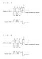
- FIG. 3is a band diagram in the vicinity of the active layer 20 of the nitride-based semiconductor laser according to this embodiment.
- the band diagram in FIG. 3indicates same reference numerals as the structure, at the position corresponding to the composition of the nitride-based semiconductor laser according to this embodiment. It is clear from FIG. 3 that the band discontinuous amount between the final barrier layer 1 and the electron blocking layer 3 is larger than the band discontinuous amount between the barrier layer 2 and the electron blocking layer 3 .
- the barrier layers 1 and 2are located adjacent to and have larger band gaps than the well layers 18 .
- the final barrier layer 1is the one that is closest to the p-side.
- the final barrier layer 1is made to have a smaller band gap than the barrier layers 2 other than the final barrier layer 1 .
- This final barrier layer 1may be configured of a plurality of layers 13 and 19 having larger band gaps than the well layers 18 , as shown in FIG. 7 which will be described later in a second preferred embodiment.
- the final barrier layer 1a layer which has a larger band gap than the well layer 18 closest to the p-side is provided between and in contact with the well layer 18 closest to the p-side and the electron blocking layer 3 .
- the band gap of this final barrier layer 1is smaller than that of the barrier layers 2 other than the final barrier layer 1 .
- a final barrier layer whose band gap is larger than that of the well layers 18 and smaller than that of the barrier layers 2may be provided between the well layer 18 closest to the p-side and an optical waveguide layer.
- a final barrier layer whose band gap is larger than that of the well layers 18 and smaller than that of the barrier layers 2may be provided between the well layer 18 closest to the p-side and a clad layer 10 .
- the surface of the GaN substrate 4is cleaned preliminarily by thermal cleaning or the like, and the n-type GaN buffer layer 5 is grown on the surface at a growth temperature of, for example, 1000° C. by a metal organic chemical vapor deposition (MOCVD) method.
- MOCVDmetal organic chemical vapor deposition
- growth temperatures of these layersare, for example, 1000° C. for the n-type AlGaN clad layer 6 and the n-type GaN optical guide layer 7 , 740° C. from the partial active layer 8 to the undoped InGaN final barrier layer 1 , and 1000° C. from the p-type AlGaN electron blocking layer 3 to the p-type GaN contact layer 11 .
- Resistis applied on the whole surface of the wafer finishing the crystal growth process, and a resist pattern (not shown) having a predetermined shape corresponding to the shape of the ridge 12 is formed by lithography.
- a resist pattern(not shown) having a predetermined shape corresponding to the shape of the ridge 12 is formed by lithography.
- the waferis etched into the layer of the p-type AlGaN clad layer 10 by, for example, an RIE (reactive ion etching) method.
- RIEreactive ion etching
- the ridge 12is manufactured as a optical waveguide structure.
- RIE etching gasfor example, chlorine gas is used.
- the SiO 2 film 14 having a thickness of, for example, 0.2 ⁇ mis formed on the entire surface of the substrate by a CVD method, a vacuum deposition method, or a sputtering method. Then, the resist pattern is removed, and the SiO 2 film on the ridge 12 is removed at the same time. After this lift-off, the opening 15 is formed on the ridge 12 .
- Pt and Au filmsare formed sequentially by, for example, a vacuum deposition method.
- a resist patternis formed for forming the p-type electrode 16 by lithography.
- the p-type electrode 16is formed by wet etching or dry etching.
- Ti and Al filmsare formed sequentially by a vacuum deposition method. Alloy is formed for ohmic contact with the n-type electrode 17 .
- This substrateis processed into a bar shape by cleavage or the like, and both resonator ends are formed, and the resonator ends are coated, and the bar is formed into a chip by cleavage. Finally, the nitride-based semiconductor laser shown in FIG. 1 is manufactured.
- LASTIPLaser Technology Integrated Program
- Crosslight Software Inc.which is a simulator operating on the principles of Maxwell equation, Poisson equation, rate equation, and the like.
- FIG. 4is a sectional view showing a configuration of a nitride-based semiconductor laser used in simulation. As shown in FIG. 4 , on the GaN substrate 4 , the GaN buffer layer 5 , the n-type AlGaN clad layer 6 , and the n-type GaN optical guide 7 having a thickness of 100 nm are formed sequentially.
- a partial active layer 8having a multiple quantum well structure consisting of three well layers of 3.5 nm in thickness and a barrier layer of 7.0 nm in thickness is formed.
- the final barrier layer 1having a thickness of 20 nm, the p-type AlGaN electron blocking layer 3 having a thickness of 20 nm and an Al composition ratio of 0.20, the p-type GaN optical guide layer 9 having a thickness of 100 nm, the p-type AlGaN clad layer 10 having a thickness of 400 nm, and the p-type GaN contact layer 11 having a thickness of 100 nm are sequentially laminated.
- the ridge 12has a width of 2.2 ⁇ m.
- the performanceis simulated in the following conditions, using InGaN having an In composition ratio of 0.02 as a material of the final barrier layer 1 and the all barrier layers 2 , using GaN having a larger band gap than that of InGaN having an In composition ratio of 0.02, and using InGaN having an In composition ratio of 0.02 only as the final barrier layer 1 while using GaN as all barrier layers 2 .
- FIGS. 5 and 6show calculation results by simulation in the above conditions.
- FIG. 5shows the rate of electrons becoming reactive current by overflow of injected electrons from the electron blocking layer 3 .
- FIG. 6shows optical output-current characteristic.
- FIGS. 5 and 6“a” shows the case of using InGaN having an In composition ratio of 0.02 as a material of the final barrier layer 1 and the all barrier layers 2 , “b” shows the case of using GaN as a material of the final barrier layer 1 and the all barrier layers 2 , and “c” shows the case of using InGaN having an In composition ratio of 0.02 as a material of only the final barrier layer 1 while using GaN as a material of the all barrier layers 2 .
- the simulation resultsuggests that the rate of overflow of electrons from the electron blocking layer 3 to the p-side is mostly determined by the band discontinuous amount of a conduction band between the final barrier layer 1 and the electron blocking layer 3 . Accordingly, when the band gap of the final barrier layer 1 is further reduced, the rate of overflow of electrons from the electron blocking layer 3 can be further decreased.
- the band gap of the final barrier layer 1is set to be smaller than the band gap of the barrier layers 2 .
- the band discontinuous amount (electron barrier) of a conduction band between the final barrier layer 1 and the electron blocking layer 3is larger, and hence electrons overflowing the electron barrier can be suppressed.
- a material of the barrier layers 2is InGaN or GaN
- a material of the final barrier layer 1is InGaN.
- the material of the barrier layers 2is InGaN or GaN
- the material of the final barrier layer 1has a smaller band gap than the band gap of the barrier layers 2 , it is possible to lower the overflow rate of electrons from the electron blocking layer 3 .
- the layer at the p-side contacting with the final barrier layer 1is AlGaN electron blocking layer 3 , but the same effects are obtained by using the optical waveguide layer 9 or the p-type clad layer 10 made of AlGaN or GaN having a smaller Al composition ratio.
- the same effectsare obtained in the nitride-based semiconductor laser of the structure not having the AlGaN electron blocking layer 3 or the optical waveguide layer 9 .
- the nitride-based semiconductor laser according to first embodimenthas the final barrier layer 1 disposed in contact with the well layer 18 .
- the final barrier layer 1is formed on the well layer 18 , deterioration in crystallinity of the well layer 18 can be prevented.
- a thickness of the final barrier layer 1is different from and thicker than those of the barrier layers 2 and well layer 18 , and the overflow rate of electrons from the electron blocking layer 3 can be further lowered.
- a nitride-based semiconductor laser according to a second embodimentis similar to the first embodiment, except that the final barrier layer 1 is formed of a plurality of partial final barrier layers 13 , 19 (not shown in FIG. 1 ).
- the partial final barrier layer 13is called a first final barrier layer disposed at the n-type clad layer 6 side
- the partial final barrier layer 19is called a second final barrier layer disposed at the p-type clad layer 6 side.
- the partial final barrier layer 13has a thickness of, for example, 10 nm, is made of InGaN having an In composition ratio of 0.02, and is formed on the partial active layer 8 .
- the partial final barrier layer 19having a thickness of 10 nm and made of InGaN having an In composition ratio of 0.04 is formed.
- FIG. 7is a band diagram in the vicinity of the active layer 20 of the nitride-based semiconductor laser according to this embodiment.
- the band diagram in FIG. 7indicates same reference numerals as the structure, at the position corresponding to the configuration of nitride-based semiconductor laser of the embodiment.
- the invention according to this embodimentis increased in the band discontinuous amount in a conduction band between the partial final barrier layer 19 and the electron blocking layer 3 .
- the band discontinuous amount in a conduction band between the partial final barrier layer 19 and the electron blocking layer 3is increased.
- a rate of electrons overflowing from electron blocking layer 3 to p-sideis mostly determined by the band discontinuous amount in a conduction band between the partial final barrier layer 19 and the electron blocking layer 3 .
- the barrier layers 2if a material having a large band gap is used for the barrier layers 2 , electrons overflowing the electron blocking layer 3 can be suppressed.
- the band gap of the partial final barrier layer 19is smaller than the band gap of the partial final barrier layer 13 adjacent to the partial final barrier layer 19 .
- the band discontinuous amount in a conduction band between the partial final barrier layer 19 and the electron blocking layer 3can be increased as compared with the case of bonding the partial final barrier layer 13 to the electron blocking layer 3 .
- a material of the partial final barrier layer 19is InGaN
- a material of the partial final barrier layer 13 adjacent to the partial final barrier layer 19is InGaN or GaN having a band gap larger than the band gap of the partial final barrier layer 19 .
- the band discontinuous amount in a conduction band between the partial final barrier layer 19 and the electron blocking layer 3can be increased as compared with the case of bonding the partial final barrier layer 13 to the electron blocking layer 3 .
- the band gap of the partial final barrier layer 13may be the same or almost same as the band gap of the barrier layer 2 other than the final barrier layer 1 .
- band gaps of the partial final barrier layer 13is the same or almost same as the band gap of the barrier layer 2 , band shapes are almost same in all of the well layers 18 , and quantum levels formed in the well layers 18 may be almost the same. As a result, the threshold current is decreased and differential efficiency is enhanced.
- the final barrier layer 1approaches the electron blocking layer 3 from the side closer to the well layer 18 , and is made of InGaN of which In composition ratio increases continuously from 0.02 to 0.04.
- FIG. 8is a band diagram in the vicinity of the active layer 20 of the nitride-based semiconductor laser according to this embodiment. As shown in FIG. 8 , the band gap of the final barrier layer 1 decreases continuously as approaching the electron blocking layer 3 , and at the position contacting with the electron blocking layer 3 , the band gap is smaller than the band gap of barrier layer 2 .
- a rate of electrons overflowing from electron blocking layer 3is mostly determined by the band discontinuous amount in a conduction band at the contacting position of the final barrier layer 1 and the electron blocking layer 3 , and therefore, in this embodiment, same effects as in the first embodiment can be obtained.
- the material of the final barrier layer 1is not limited to InGaN, but any material may be used as far as the band gap is smaller than the band gap of the barrier layer 2 at the position contacting with the electron blocking layer 3 .
- barrier layers 2are made of In x Al y Ga 1-x-y N (0 ⁇ x ⁇ 1 0 ⁇ y ⁇ 1, x+y ⁇ 1). Other configuration is same as in the first to third embodiments, and duplicate explanation is omitted.
- the band gap of the barrier layers 2is set larger than the case where InGaN is used.
- overflow of electrons from a well layer 18can be further suppressed.
- the nitride-based semiconductor light-emitting device of further excellent differential characteristiccan be obtained.
- a nitride-based semiconductor laser according to a fifth embodimentis similar to the nitride-based semiconductor lasers according to the first to third embodiments, except that the barrier layers 2 are made of GaN.
- the band gap of the barrier layers 2is larger than when InGaN is used, and the barrier layers of excellent crystalline quality can be obtained. Hence, the nitride-based semiconductor laser having excellent differential characteristic can be obtained.
Landscapes
- Physics & Mathematics (AREA)
- Optics & Photonics (AREA)
- Engineering & Computer Science (AREA)
- General Physics & Mathematics (AREA)
- Electromagnetism (AREA)
- Condensed Matter Physics & Semiconductors (AREA)
- Chemical & Material Sciences (AREA)
- Nanotechnology (AREA)
- Life Sciences & Earth Sciences (AREA)
- Biophysics (AREA)
- Geometry (AREA)
- Crystallography & Structural Chemistry (AREA)
- Semiconductor Lasers (AREA)
- Electrodes Of Semiconductors (AREA)
- Led Devices (AREA)
Abstract
Description
- 1. Field of the Invention
- The present invention relates to a semiconductor light-emitting device using a nitride-based III-V group compound semiconductor.
- 2. Description of the Background Art
- Recently, as a semiconductor laser which enables light emission in a range from a blue region to an ultraviolet region, which is required for making the density of an optical disc high, a nitride-based semiconductor laser using a nitride-based III-V group compound semiconductor has been intensively researched and developed, and has been already put in use.
- In the nitride-based semiconductor laser reported so far, as its active layer structure, there has been frequently adopted a multiple quantum well structure that two or more well layers made of InGaN and three or more barrier layers made of InGaN having smaller In composition ratio than that of the above InGaN (usually about 0.02) are laminated alternately.
- In the nitride-based III-V group compound semiconductor, a ratio of a band discontinuous amount of a conduction band and a band discontinuous amount of a valence band when hetero junction is formed is about 2.5:7.5, and it is known that the band discontinuous amount of conduction band is very small (see Applied Physics Letter vol. 70 (1997), p. 2577). Accordingly, electrons are likely to overflow from the well layer beyond the barrier layer, which often leads to problems such as increase in threshold current, and deterioration of differential efficiency and temperature characteristic.
- In order to solve these problems, it may be considered to increase the band discontinuous amount of the conduction band by widening the band gap of the barrier layer as much as possible. For this purpose, InGaN having smaller In composition ratio may be used as the barrier layer, or a material (substance) having larger band gap than that of InGaN may be used, such as GaN, AlGaN or InAlGaN.
- When the band gap of the barrier layer is widened, the band discontinuous amount of the valence band is increased. However, as barrier layer, when InGaN having smallest In composition ratio is used or when GaN or AlGaN is used, these materials are smaller in lattice constant at wider band gap, and are exposed to greater tensile distortion. According to the band properties of semiconductor receiving this distortion, the band discontinuous amount of the valence band is not increased so much as compared with increase of the band discontinuous amount of the conduction band.
- As a result, it is considered that the problem of overflow of electrons can be solved without causing a problem of difficulty in uniform injection of holes in the wells of two layers or more.
- The conventional art related to the present invention is disclosed in Japanese Patent Application Laid-Open No. 07-170022 (1995).
- However, the present inventor has confirmed by simulation that a new problem arises when a barrier layer is made of a material having larger band gap, electrons are likely to overflow beyond the electron blocking layer from a final barrier layer which is closest to the p-side. It is considered that this problem is caused due to the following reason: the barrier layer is made of a material having larger band gap, so that a band discontinuous amount (electron barrier) between the final barrier layer and the electron blocking layer becomes small.
- Further, in the case of barrier layer of InGaN of smaller band gap than GaN or AlGaN, rate of electrons overflowing the electron barrier from the final barrier layer is not zero, which may lead to deterioration of threshold current of semiconductor light-emitting device, differential efficiency, and temperature characteristics.
- Accordingly, omitting the final barrier layer, by bonding the well layer and electron blocking layer directly, it may be considered to reduce the overflowing electrons by increasing the height of electron barrier, than in the case of presence of final barrier layer.
- However, a film forming temperature of an electron blocking layer is higher than that of a well layer by about 200° C. Therefore, if attempted to form an electron blocking layer directly on the well layer, after forming the well layer, the film forming temperature must be raised without protecting the surface of the well layer. In this process, crystallinity of the well layer surface deteriorates.
- When a semiconductor light-emitting device is manufactured by using such a well layer deteriorated in crystallinity, electrons trapped in the well layer do not contribute to laser oscillation, and threshold current or differential efficiency may be worsened.
- It is an object of the present invention to provide a semiconductor light-emitting device which exhibits small threshold current, high differential efficiency and good characteristics, by reducing electrons that overflow an electron barrier for trapping the electrons in an active layer.
- According to a first aspect of the present invention, a semiconductor light-emitting device has a structure that an active layer is interposed between an n-type clad layer and a p-type clad layer and uses a nitride-based III-V group compound semiconductor.
- The active layer has a plurality of barrier layers, and a well layer formed so as to be interposed between the barrier layers.
- Of the plurality of barrier layers, a final barrier layer closest to the p-type clad layer side has a smaller band gap than that a barrier layer other than the final barrier layer.
- According to the present invention, the band gap of the final barrier layer is made smaller than the band gap of the barrier layer other than the final barrier layer. Accordingly, an electron barrier formed between the barrier layer and the p-type clad layer is set larger than a case where the barrier layer other than final barrier layer is used as a final barrier layer. As a result, electrons overflowing the electron barrier from the active layer can be reduced.
- Besides, since the final barrier layer is formed on the well layer, it is free from problem of deterioration in crystallinity of the well layer.
- According to the second aspect of the present invention, a semiconductor light-emitting device has a structure that an active layer is interposed between an n-type clad layer and a p-type clad layer and uses a nitride-based III-V group compound semiconductor.
- The active layer has a plurality of barrier layers, and a well layer formed alternately to the barrier layers.
- The semiconductor light-emitting device includes a first layer which is provided between the plurality of barrier layers and the p-type clad layer and has a band gap smaller than those of the plurality of barrier layers and larger than that of the well layer.
- According to the present invention, the band gap of the first layer is smaller than those of the plurality of barrier layers. As a result, as compared with the electron barrier formed between the barrier layer and the p-type clad layer, the electron barrier formed between the first layer and the p-type clad layer can be formed larger; therefore, electrons overflowing the electron barrier from the active layer can be reduced.
- These and other objects, features, aspects and advantages of the present invention will become more apparent from the following detailed description of the present invention when taken in conjunction with the accompanying drawings.
FIG. 1 is a sectional view showing a configuration of a nitride-based semiconductor laser according to a first embodiment;FIG. 2 is a sectional view showing a configuration of a partial active layer of the nitride-based semiconductor laser according to the first embodiment;FIG. 3 is a band diagram of the nitride-based semiconductor laser according to the first embodiment;FIG. 4 is a sectional view showing a configuration of a semiconductor light-emitting device used in simulation according to the first embodiment;FIG. 5 shows simulation results of optical an output-current characteristic in the nitride-based semiconductor laser according to the first embodiment;FIG. 6 shows simulation results of an electron overflow rate in the nitride-based semiconductor laser according to the first embodiment;FIG. 7 is a band diagram of a nitride-based semiconductor laser according to a second embodiment; andFIG. 8 is a band diagram of a nitride-based semiconductor laser according to a third embodiment.FIG. 1 is a sectional view showing a configuration of a nitride-based semiconductor laser (semiconductor light-emitting device) according to a first embodiment. This nitride-based semiconductor laser has a ridge structure and an SCH structure.- As shown in
FIG. 1 , the nitride-based semiconductor laser according to this embodiment has an n-typeGaN buffer layer 5 formed on a Ga surface which is a main surface of aGaN substrate 4. This layer is formed for the purpose of reducing surface undulations on theGaN substrate 4 and laminating the upper layers flatly as much as possible. - On the n-type
GaN buffer layer 5, an n-type AlGaN clad layer (n-type clad layer)6, an n-type GaNoptical guide layer 7 as an n-side guide layer, anactive layer 20, a p-type AlGaN electron blocking layer3 (electron blocking layer, blocking layer), a p-type GaNoptical guide layer 9 as a p-side guide layer, a p-type AlGaN clad layer (p-type clad layer)10, and a p-type GaN contact layer (p-type contact layer)11 are laminated sequentially. - Herein, the p-type GaN
optical guide layer 9 is selected so as to make a band gap larger than those of afinal barrier layer 1 and abarrier layer 2 which will be described later. The p-type GaNoptical guide layer 9 is provided in contact with theactive layer 20 side of the p-type clad layer 10. - The n-type
GaN buffer layer 5 has a thickness of, for example, 1 μm, and silicon (Si) doped as n-type impurity. The n-typeAlGaN clad layer 6 has a thickness of, for example, 1 μm, Si doped as n-type impurity, and an Al composition ratio of, for example, 0.07. - The
active layer 20 includes a plurality of barrier layers, and a plurality of well layers formed so as to be interposed between the plurality of barrier layers, and constitute a multiple quantum well structure. Of the plurality of barrier layers, the barrier layer which is closest to the p-type clad layer 10 side corresponds to thefinal barrier layer 1. FIG. 2 is a sectional view of a partialactive layer 8 configuring theactive layer 20. The partialactive layer 8 has a configuration in that abarrier layer 2 made of InxGa1-xN (x=0.02) (barrier layer other than the final barrier layer1), and awell layer 18 made of InyGa1-yN (y=0.14) are laminated alternately. A thickness of thebarrier layer 2 is, for example, 7 nm, and a thickness of thewell layer 18 is, for example, 3.5 nm.- The
final barrier layer 1 is formed of undoped InzGa1-zN having a thickness of 20 nm. An In composition ratio z is, for example, 0.04. The In composition ratio z offinal barrier layer 1 is larger than the In composition ratio x (=0.02) of theother barrier layer 2, and the band gap is smaller than the band gap of thebarrier layer 2. - Hence, the In composition ratios x, y, z satisfy the relation of 0<x<z<y<1. Also the In composition ratios x, y, z satisfy the relation of (y−z)>(z−x).
- The
final barrier layer 1 is selected to be different in thickness and large in thickness of thebarrier layer 2 and thewell layer 18. - In this example of this embodiment, the number of wells of the
active layer 20 is three. - The p-type AlGaN
electron blocking layer 3 has a thickness of, for example, 10 nm, and an In composition ratio of, for example, 0.18. The p-type GaNoptical guide layer 9 has a thickness of, for example, 100 nm. The p-type AlGaN cladlayer 10 has a thickness of, for example, 400 nm, Mg doped as p-type impurity, and an Al composition ratio of, for example, 0.07. The p-typeGaN contact layer 11 has a thickness of, for example, 100 nm, and Mg doped as p-type impurity. Ridges 12 are formed in the p-type AlGaN cladlayer 10 and the p-type contact layer 11 by etching, for example, in a direction of (1-100). Theridge 12 has a width of, for example, 2.2 μm.- The
ridge 12 is formed on theGaN substrate 4 at a position corresponding to a low defect region located between high dislocation regions of several microns to tens of microns in width formed in a stripe. To protect the surface or insulate electrically at the side or lateral bottom side of theridge 12, an insulatingfilm 14 such as an SiO2film having a thickness of, for example, 200 nm is formed so as to cover theridge 12. - In the insulating
film 14, the portion formed on theridge 12 has anopening 15. By thisopening 15, electrical contact between the p-type electrode 16 and the p-type contact layer 11 is established. - The p-
type electrode 16 has a structure, for example, that Pd and Au films are sequentially laminated. On the N surface at the opposite side of the Ga surface, that is, the main surface of theGaN substrate 4, an n-type electrode 17 is formed. The n-type electrode 17 has a structure that, for example, Ti and Au films are sequentially laminated. FIG. 3 is a band diagram in the vicinity of theactive layer 20 of the nitride-based semiconductor laser according to this embodiment. The band diagram inFIG. 3 indicates same reference numerals as the structure, at the position corresponding to the composition of the nitride-based semiconductor laser according to this embodiment. It is clear fromFIG. 3 that the band discontinuous amount between thefinal barrier layer 1 and theelectron blocking layer 3 is larger than the band discontinuous amount between thebarrier layer 2 and theelectron blocking layer 3.- In
FIG. 3 , the barrier layers1 and2 are located adjacent to and have larger band gaps than the well layers18. Of those barrier layers, thefinal barrier layer 1 is the one that is closest to the p-side. In the first preferred embodiment, thefinal barrier layer 1 is made to have a smaller band gap than the barrier layers2 other than thefinal barrier layer 1. Thisfinal barrier layer 1 may be configured of a plurality oflayers FIG. 7 which will be described later in a second preferred embodiment. - In
FIG. 3 , as thefinal barrier layer 1, a layer which has a larger band gap than thewell layer 18 closest to the p-side is provided between and in contact with thewell layer 18 closest to the p-side and theelectron blocking layer 3. The band gap of thisfinal barrier layer 1 is smaller than that of the barrier layers2 other than thefinal barrier layer 1. - If there is no
electron blocking layer 3 provided, a final barrier layer whose band gap is larger than that of the well layers18 and smaller than that of the barrier layers2 may be provided between thewell layer 18 closest to the p-side and an optical waveguide layer. Or, if there is noelectron blocking layer 3 and no optical waveguide layer provided, a final barrier layer whose band gap is larger than that of the well layers18 and smaller than that of the barrier layers2 may be provided between thewell layer 18 closest to the p-side and aclad layer 10. - A manufacturing method of the semiconductor light-emitting device according to this embodiment is explained.
- At first, the surface of the
GaN substrate 4 is cleaned preliminarily by thermal cleaning or the like, and the n-typeGaN buffer layer 5 is grown on the surface at a growth temperature of, for example, 1000° C. by a metal organic chemical vapor deposition (MOCVD) method. - Thereafter, by the same MOCVD method, the n-type AlGaN clad
layer 6, the n-type GaNoptical guide layer 7, the partialactive layer 8 having an undoped InxGa1-xN/InyGa1-yN multiple quantum well structure, thefinal barrier layer 1 made of undoped InGaN, the p-type AlGaNelectron blocking layer 3, the p-type GaNoptical guide layer 9, the p-type AlGaN cladlayer 10, and the p-type GaN cladlayer 11 are laminated sequentially. - Herein; growth temperatures of these layers are, for example, 1000° C. for the n-type AlGaN clad
layer 6 and the n-type GaNoptical guide layer 7, 740° C. from the partialactive layer 8 to the undoped InGaNfinal barrier layer 1, and 1000° C. from the p-type AlGaNelectron blocking layer 3 to the p-typeGaN contact layer 11. - Resist is applied on the whole surface of the wafer finishing the crystal growth process, and a resist pattern (not shown) having a predetermined shape corresponding to the shape of the
ridge 12 is formed by lithography. Using this resist pattern as a mask, the wafer is etched into the layer of the p-type AlGaN cladlayer 10 by, for example, an RIE (reactive ion etching) method. By this etching, theridge 12 is manufactured as a optical waveguide structure. As RIE etching gas, for example, chlorine gas is used. - Next, without removing the resist pattern used as mask, the SiO2film14 having a thickness of, for example, 0.2 μm is formed on the entire surface of the substrate by a CVD method, a vacuum deposition method, or a sputtering method. Then, the resist pattern is removed, and the SiO2film on the
ridge 12 is removed at the same time. After this lift-off, theopening 15 is formed on theridge 12. - Next, on the entire surface of substrate, Pt and Au films are formed sequentially by, for example, a vacuum deposition method. In succession, after applying the resist, a resist pattern is formed for forming the p-
type electrode 16 by lithography. Using the resist pattern as a mask, the p-type electrode 16 is formed by wet etching or dry etching. - Thereafter, on the front side of reverse surface of substrate, Ti and Al films are formed sequentially by a vacuum deposition method. Alloy is formed for ohmic contact with the n-
type electrode 17. - This substrate is processed into a bar shape by cleavage or the like, and both resonator ends are formed, and the resonator ends are coated, and the bar is formed into a chip by cleavage. Finally, the nitride-based semiconductor laser shown in
FIG. 1 is manufactured. - The following is the explanation of simulation results about characteristics of the nitride-based semiconductor laser according to this embodiment.
- One example of the semiconductor laser simulator used herein is a LASTIP (Laser Technology Integrated Program) commercially available from Crosslight Software Inc., which is a simulator operating on the principles of Maxwell equation, Poisson equation, rate equation, and the like.
FIG. 4 is a sectional view showing a configuration of a nitride-based semiconductor laser used in simulation. As shown inFIG. 4 , on theGaN substrate 4, theGaN buffer layer 5, the n-type AlGaN cladlayer 6, and the n-type GaNoptical guide 7 having a thickness of 100 nm are formed sequentially.- On the n-type GaN
optical guide layer 7, a partialactive layer 8 having a multiple quantum well structure consisting of three well layers of 3.5 nm in thickness and a barrier layer of 7.0 nm in thickness is formed. - Further, the
final barrier layer 1 having a thickness of 20 nm, the p-type AlGaNelectron blocking layer 3 having a thickness of 20 nm and an Al composition ratio of 0.20, the p-type GaNoptical guide layer 9 having a thickness of 100 nm, the p-type AlGaN cladlayer 10 having a thickness of 400 nm, and the p-typeGaN contact layer 11 having a thickness of 100 nm are sequentially laminated. Theridge 12 has a width of 2.2 μm. - In the nitride-based semiconductor laser having the aforementioned structure, the performance is simulated in the following conditions, using InGaN having an In composition ratio of 0.02 as a material of the
final barrier layer 1 and the allbarrier layers 2, using GaN having a larger band gap than that of InGaN having an In composition ratio of 0.02, and using InGaN having an In composition ratio of 0.02 only as thefinal barrier layer 1 while using GaN as all barrier layers2. FIGS. 5 and 6 show calculation results by simulation in the above conditions.FIG. 5 shows the rate of electrons becoming reactive current by overflow of injected electrons from theelectron blocking layer 3.FIG. 6 shows optical output-current characteristic.- In
FIGS. 5 and 6 , “a” shows the case of using InGaN having an In composition ratio of 0.02 as a material of thefinal barrier layer 1 and the allbarrier layers 2, “b” shows the case of using GaN as a material of thefinal barrier layer 1 and the allbarrier layers 2, and “c” shows the case of using InGaN having an In composition ratio of 0.02 as a material of only thefinal barrier layer 1 while using GaN as a material of the all barrier layers2. - As shown in “b” in
FIG. 5 , when a material of a wide band gap (GaN) is used in all of thefinal barrier 1 andbarrier layers 2, the rate of overflow of electrons from theelectron blocking layer 3 to the p-side is increased. As a result, as shown in “b” inFIG. 6 , elevation of threshold current and drop of differential efficiency are observed. - However, as shown in “c” in
FIG. 5 , when a material having a smaller band gap than that of the barrier layers2 (InGaN: In composition ratio 0.02) is used for thefinal barrier layer 1, the rate of overflow of electrons from theelectron blocking layer 3 is considerably decreased. As a result, as shown in “c” inFIG. 6 , threshold current is decreased, and differential efficiency is increased. - By using GaN having a large band gap for the barrier layers2, electrons overflowing the barrier layers2 from the
well layer 18 can be decreased, and the differential efficiency is further improved as compared with the case “a”. - The simulation result suggests that the rate of overflow of electrons from the
electron blocking layer 3 to the p-side is mostly determined by the band discontinuous amount of a conduction band between thefinal barrier layer 1 and theelectron blocking layer 3. Accordingly, when the band gap of thefinal barrier layer 1 is further reduced, the rate of overflow of electrons from theelectron blocking layer 3 can be further decreased. - As explained herein, in the semiconductor light-emitting device according to this embodiment, the band gap of the
final barrier layer 1 is set to be smaller than the band gap of the barrier layers2. - As compared with the case of using the same material as the barrier layers2 in the
final barrier layer 1, the band discontinuous amount (electron barrier) of a conduction band between thefinal barrier layer 1 and theelectron blocking layer 3 is larger, and hence electrons overflowing the electron barrier can be suppressed. - In
FIGS. 5 and 6 , a material of the barrier layers2 is InGaN or GaN, and a material of thefinal barrier layer 1 is InGaN. However, regardless of the material of the barrier layers2, as far as the material of thefinal barrier layer 1 has a smaller band gap than the band gap of the barrier layers2, it is possible to lower the overflow rate of electrons from theelectron blocking layer 3. - In this embodiment, the layer at the p-side contacting with the
final barrier layer 1 is AlGaNelectron blocking layer 3, but the same effects are obtained by using theoptical waveguide layer 9 or the p-type cladlayer 10 made of AlGaN or GaN having a smaller Al composition ratio. - That is, the same effects are obtained in the nitride-based semiconductor laser of the structure not having the AlGaN
electron blocking layer 3 or theoptical waveguide layer 9. - The nitride-based semiconductor laser according to first embodiment has the
final barrier layer 1 disposed in contact with thewell layer 18. - Since the
final barrier layer 1 is formed on thewell layer 18, deterioration in crystallinity of thewell layer 18 can be prevented. - A thickness of the
final barrier layer 1 is different from and thicker than those of the barrier layers2 andwell layer 18, and the overflow rate of electrons from theelectron blocking layer 3 can be further lowered. - A nitride-based semiconductor laser according to a second embodiment is similar to the first embodiment, except that the
final barrier layer 1 is formed of a plurality of partial final barrier layers13,19 (not shown inFIG. 1 ). - Herein, the partial
final barrier layer 13 is called a first final barrier layer disposed at the n-type cladlayer 6 side, and the partialfinal barrier layer 19 is called a second final barrier layer disposed at the p-type cladlayer 6 side. - The partial
final barrier layer 13 has a thickness of, for example, 10 nm, is made of InGaN having an In composition ratio of 0.02, and is formed on the partialactive layer 8. On the partialfinal barrier layer 13, the partialfinal barrier layer 19 having a thickness of 10 nm and made of InGaN having an In composition ratio of 0.04 is formed. - Other configuration is same as in the nitride-based semiconductor laser according to the first embodiment, and duplicate explanation is omitted.
FIG. 7 is a band diagram in the vicinity of theactive layer 20 of the nitride-based semiconductor laser according to this embodiment. The band diagram inFIG. 7 indicates same reference numerals as the structure, at the position corresponding to the configuration of nitride-based semiconductor laser of the embodiment.- As shown in
FIG. 7 , the invention according to this embodiment is increased in the band discontinuous amount in a conduction band between the partialfinal barrier layer 19 and theelectron blocking layer 3. - That is, by setting the band gap of the partial
final barrier layer 19 smaller than the band gap of thebarrier layer 2 other than thefinal barrier layer 1, the band discontinuous amount in a conduction band between the partialfinal barrier layer 19 and theelectron blocking layer 3 is increased. - A rate of electrons overflowing from
electron blocking layer 3 to p-side is mostly determined by the band discontinuous amount in a conduction band between the partialfinal barrier layer 19 and theelectron blocking layer 3. - Accordingly, as in the first embodiment, if a material having a large band gap is used for the barrier layers2, electrons overflowing the
electron blocking layer 3 can be suppressed. - In the semiconductor light-emitting device according to the second embodiment, the band gap of the partial
final barrier layer 19 is smaller than the band gap of the partialfinal barrier layer 13 adjacent to the partialfinal barrier layer 19. - Accordingly, the band discontinuous amount in a conduction band between the partial
final barrier layer 19 and theelectron blocking layer 3 can be increased as compared with the case of bonding the partialfinal barrier layer 13 to theelectron blocking layer 3. - As a result, electrons overflowing the
electron blocking layer 3 can be suppressed. - In the semiconductor light-emitting device according to the second embodiment, a material of the partial
final barrier layer 19 is InGaN, and a material of the partialfinal barrier layer 13 adjacent to the partialfinal barrier layer 19 is InGaN or GaN having a band gap larger than the band gap of the partialfinal barrier layer 19. - Accordingly, the band discontinuous amount in a conduction band between the partial
final barrier layer 19 and theelectron blocking layer 3 can be increased as compared with the case of bonding the partialfinal barrier layer 13 to theelectron blocking layer 3. - As a result, electrons overflowing the
electron blocking layer 3 can be suppressed. - The band gap of the partial
final barrier layer 13 may be the same or almost same as the band gap of thebarrier layer 2 other than thefinal barrier layer 1. - When the band gap of the partial
final barrier layer 13 is the same or almost same as the band gap of thebarrier layer 2, band shapes are almost same in all of the well layers18, and quantum levels formed in the well layers18 may be almost the same. As a result, the threshold current is decreased and differential efficiency is enhanced. - In a nitride-based semiconductor laser according to a third embodiment, the
final barrier layer 1 approaches theelectron blocking layer 3 from the side closer to thewell layer 18, and is made of InGaN of which In composition ratio increases continuously from 0.02 to 0.04. - Other configuration is same as in the nitride-based semiconductor laser according to the first embodiment, and duplicate explanation is omitted.
FIG. 8 is a band diagram in the vicinity of theactive layer 20 of the nitride-based semiconductor laser according to this embodiment. As shown inFIG. 8 , the band gap of thefinal barrier layer 1 decreases continuously as approaching theelectron blocking layer 3, and at the position contacting with theelectron blocking layer 3, the band gap is smaller than the band gap ofbarrier layer 2.- A rate of electrons overflowing from
electron blocking layer 3 is mostly determined by the band discontinuous amount in a conduction band at the contacting position of thefinal barrier layer 1 and theelectron blocking layer 3, and therefore, in this embodiment, same effects as in the first embodiment can be obtained. - The material of the
final barrier layer 1 is not limited to InGaN, but any material may be used as far as the band gap is smaller than the band gap of thebarrier layer 2 at the position contacting with theelectron blocking layer 3. - In a fourth embodiment, barrier layers2 are made of InxAlyGa1-x-yN (0≦x<1 0≦y≦1, x+y≦1). Other configuration is same as in the first to third embodiments, and duplicate explanation is omitted.
- By using InxAlyGa1-x-yN in the barrier layers2, the band gap of the barrier layers2 is set larger than the case where InGaN is used. As a result, overflow of electrons from a
well layer 18 can be further suppressed. Hence, as compared with the first to third embodiments, the nitride-based semiconductor light-emitting device of further excellent differential characteristic can be obtained. - A nitride-based semiconductor laser according to a fifth embodiment is similar to the nitride-based semiconductor lasers according to the first to third embodiments, except that the barrier layers2 are made of GaN.
- By using GaN in the barrier layers2, the band gap of the barrier layers2 is larger than when InGaN is used, and the barrier layers of excellent crystalline quality can be obtained. Hence, the nitride-based semiconductor laser having excellent differential characteristic can be obtained.
- While the invention has been shown and described in detail, the foregoing description is in all aspects illustrative and not restrictive. It is therefore understood that numerous modifications and variations can be devised without departing from the scope of the invention.
Claims (27)
Applications Claiming Priority (4)
| Application Number | Priority Date | Filing Date | Title |
|---|---|---|---|
| JP2004325924 | 2004-11-10 | ||
| JP2004-325924 | 2004-11-10 | ||
| JP2005311027AJP3857295B2 (en) | 2004-11-10 | 2005-10-26 | Semiconductor light emitting device |
| JP2005-311027 | 2005-10-26 |
Publications (2)
| Publication Number | Publication Date |
|---|---|
| US20060097242A1true US20060097242A1 (en) | 2006-05-11 |
| US7745841B2 US7745841B2 (en) | 2010-06-29 |
Family
ID=36315406
Family Applications (1)
| Application Number | Title | Priority Date | Filing Date |
|---|---|---|---|
| US11/269,626ActiveUS7745841B2 (en) | 2004-11-10 | 2005-11-09 | Semiconductor light-emitting device |
Country Status (4)
| Country | Link |
|---|---|
| US (1) | US7745841B2 (en) |
| JP (1) | JP3857295B2 (en) |
| KR (1) | KR100770438B1 (en) |
| TW (1) | TWI277264B (en) |
Cited By (11)
| Publication number | Priority date | Publication date | Assignee | Title |
|---|---|---|---|---|
| US20070284564A1 (en)* | 2005-09-13 | 2007-12-13 | Sony Corporation | Gan-Based Semiconductor Light-Emitting Device, Light Illuminator, Image Display Planar Light Source Device, and Liquid Crystal Display Assembly |
| DE102009040438A1 (en)* | 2009-07-24 | 2011-01-27 | Osram Opto Semiconductors Gmbh | Optoelectronic semiconductor body with a quantum well structure |
| US20110042713A1 (en)* | 2008-03-26 | 2011-02-24 | Panasonic Electric Works Co., Ltd. | Nitride semi-conductive light emitting device |
| US20120267641A1 (en)* | 2009-12-31 | 2012-10-25 | Huo Dongming | Epitaxial wafer for light emitting diode, light emitting diode chip and methods for manufacturing the same |
| US20160005919A1 (en)* | 2013-02-05 | 2016-01-07 | Tokuyama Corporation | Nitride semiconductor light emitting device |
| US20160118537A1 (en)* | 2014-10-23 | 2016-04-28 | Stanley Electric Co., Ltd. | Semiconductor light-emitting element |
| US20160352077A1 (en)* | 2015-05-26 | 2016-12-01 | Nichia Corporation | Semiconductor laser device |
| CN106207754A (en)* | 2016-09-20 | 2016-12-07 | 山东浪潮华光光电子股份有限公司 | A kind of GaN base laser epitaxial structure and growing method thereof |
| WO2017125505A1 (en)* | 2016-01-21 | 2017-07-27 | Osram Opto Semiconductors Gmbh | Optoelectronic semiconductor chip and method for producing an optoelectronic semiconductor chip |
| DE102016111929A1 (en)* | 2016-06-29 | 2018-01-04 | Osram Opto Semiconductors Gmbh | Optoelectronic semiconductor body and light emitting diode |
| CN115425125A (en)* | 2022-09-28 | 2022-12-02 | 安徽三安光电有限公司 | Light-emitting diodes and light-emitting devices |
Families Citing this family (15)
| Publication number | Priority date | Publication date | Assignee | Title |
|---|---|---|---|---|
| JP2007080896A (en)* | 2005-09-12 | 2007-03-29 | Sanyo Electric Co Ltd | Semiconductor element |
| JP4926565B2 (en)* | 2006-06-29 | 2012-05-09 | ローム株式会社 | Semiconductor light emitting device |
| KR101252556B1 (en)* | 2006-07-26 | 2013-04-08 | 엘지이노텍 주식회사 | Nitride based light emitting diode |
| KR100842288B1 (en)* | 2006-12-08 | 2008-06-30 | 한국전자통신연구원 | Interband Tunneling Subband Transition Semiconductor Laser |
| KR100868205B1 (en)* | 2007-07-30 | 2008-11-12 | 서울옵토디바이스주식회사 | Light Emitting Diodes with Active Region of Multi-quantum Well Structure |
| KR100946034B1 (en) | 2008-02-01 | 2010-03-09 | 삼성전기주식회사 | Nitride Semiconductor Light Emitting Device |
| JP5315899B2 (en)* | 2008-09-30 | 2013-10-16 | 信越半導体株式会社 | Light emitting element |
| KR101025971B1 (en) | 2008-12-10 | 2011-03-30 | 삼성엘이디 주식회사 | Nitride semiconductor light emitting device |
| JP5641173B2 (en)* | 2009-02-27 | 2014-12-17 | 独立行政法人理化学研究所 | Optical semiconductor device and manufacturing method thereof |
| US8143614B2 (en)* | 2009-04-22 | 2012-03-27 | Dr. Samal's Lab LLC | GaN based light emitters with band-edge aligned carrier blocking layers |
| EP2408028B1 (en)* | 2010-07-16 | 2015-04-08 | LG Innotek Co., Ltd. | Light emitting device |
| KR101945808B1 (en)* | 2012-08-06 | 2019-02-08 | 엘지이노텍 주식회사 | Light emitting device and light emitting device package |
| JP2015188048A (en)* | 2014-03-10 | 2015-10-29 | 株式会社東芝 | Nitride semiconductor laminate and semiconductor light-emitting element |
| JP2016219587A (en) | 2015-05-20 | 2016-12-22 | ソニー株式会社 | Semiconductor optical device |
| JP6477642B2 (en)* | 2016-09-23 | 2019-03-06 | 日亜化学工業株式会社 | Light emitting element |
Citations (24)
| Publication number | Priority date | Publication date | Assignee | Title |
|---|---|---|---|---|
| US895415A (en)* | 1908-03-06 | 1908-08-11 | Union Steel Casting Company | Annealing-box. |
| US5195969A (en)* | 1991-04-26 | 1993-03-23 | Boston Scientific Corporation | Co-extruded medical balloons and catheter using such balloons |
| US5270086A (en)* | 1989-09-25 | 1993-12-14 | Schneider (Usa) Inc. | Multilayer extrusion of angioplasty balloons |
| US5544188A (en)* | 1993-12-16 | 1996-08-06 | Mitsubishi Denki Kabushiki Kaisha | Semiconductor laser device having a high emission efficiency and a large modulation bandwidth |
| US5674242A (en)* | 1995-06-06 | 1997-10-07 | Quanam Medical Corporation | Endoprosthetic device with therapeutic compound |
| US6018095A (en)* | 1996-06-14 | 2000-01-25 | Bioland | Method for preparing an implantable composite material, resulting material, implant including said material, and kit therefor |
| US6287331B1 (en)* | 1992-03-31 | 2001-09-11 | Boston Scientific Corporation | Tubular medical prosthesis |
| US6364902B1 (en)* | 1998-10-05 | 2002-04-02 | Noble-Met, Ltd. | Metal composite tube for biomedical applications |
| US6387121B1 (en)* | 1996-10-21 | 2002-05-14 | Inflow Dynamics Inc. | Vascular and endoluminal stents with improved coatings |
| US20020144757A1 (en)* | 2000-07-07 | 2002-10-10 | Craig Charles Horace | Stainless steel alloy with improved radiopaque characteristics |
| US20020197178A1 (en)* | 1997-04-15 | 2002-12-26 | Yan John Y. | Medicated porous metal prosthesis |
| US20030018380A1 (en)* | 2000-07-07 | 2003-01-23 | Craig Charles H. | Platinum enhanced alloy and intravascular or implantable medical devices manufactured therefrom |
| US20030060873A1 (en)* | 2001-09-19 | 2003-03-27 | Nanomedical Technologies, Inc. | Metallic structures incorporating bioactive materials and methods for creating the same |
| US20030077200A1 (en)* | 2000-07-07 | 2003-04-24 | Craig Charles H. | Enhanced radiopaque alloy stent |
| US6563850B1 (en)* | 1997-10-06 | 2003-05-13 | Sharp Kabushiki Kaisha | Light-emitting device and fabricating method thereof |
| US20030185895A1 (en)* | 2002-03-29 | 2003-10-02 | Janel Lanphere | Drug delivery particle |
| US20040044397A1 (en)* | 2002-08-28 | 2004-03-04 | Stinson Jonathan S. | Medical devices and methods of making the same |
| US6726712B1 (en)* | 1999-05-14 | 2004-04-27 | Boston Scientific Scimed | Prosthesis deployment device with translucent distal end |
| US20040098089A1 (en)* | 2002-11-19 | 2004-05-20 | Jan Weber | Medical devices |
| US20040143317A1 (en)* | 2003-01-17 | 2004-07-22 | Stinson Jonathan S. | Medical devices |
| US20040237282A1 (en)* | 2003-06-02 | 2004-12-02 | Hines Richard A. | Process for forming a porous drug delivery layer |
| US20050070990A1 (en)* | 2003-09-26 | 2005-03-31 | Stinson Jonathan S. | Medical devices and methods of making same |
| US20050075408A1 (en)* | 1994-05-13 | 2005-04-07 | Ringeisen Timothy A. | Method for making a porous polymeric material |
| US20060153729A1 (en)* | 2005-01-13 | 2006-07-13 | Stinson Jonathan S | Medical devices and methods of making the same |
Family Cites Families (11)
| Publication number | Priority date | Publication date | Assignee | Title |
|---|---|---|---|---|
| JP3505379B2 (en) | 1997-02-21 | 2004-03-08 | シャープ株式会社 | Semiconductor laser device |
| JP3429446B2 (en) | 1998-03-19 | 2003-07-22 | シャープ株式会社 | Semiconductor light emitting device |
| JP3555727B2 (en) | 1997-10-06 | 2004-08-18 | シャープ株式会社 | Semiconductor laser device |
| US6469314B1 (en) | 1999-12-21 | 2002-10-22 | Lumileds Lighting U.S., Llc | Thin multi-well active layer LED with controlled oxygen doping |
| JP3636976B2 (en) | 2000-03-17 | 2005-04-06 | 日本電気株式会社 | Nitride semiconductor device and manufacturing method thereof |
| US6586762B2 (en) | 2000-07-07 | 2003-07-01 | Nichia Corporation | Nitride semiconductor device with improved lifetime and high output power |
| JP3803696B2 (en)* | 2000-11-21 | 2006-08-02 | 日亜化学工業株式会社 | Nitride semiconductor device |
| JP4075324B2 (en) | 2001-05-10 | 2008-04-16 | 日亜化学工業株式会社 | Nitride semiconductor device |
| WO2003041234A1 (en)* | 2001-11-05 | 2003-05-15 | Nichia Corporation | Semiconductor element |
| JP4401610B2 (en)* | 2001-12-28 | 2010-01-20 | 日亜化学工業株式会社 | Nitride semiconductor laser device |
| JP2004087908A (en) | 2002-08-28 | 2004-03-18 | Sharp Corp | Nitride semiconductor light emitting device, method of manufacturing the same, and optical device equipped with the same |
- 2005
- 2005-10-26JPJP2005311027Apatent/JP3857295B2/ennot_activeExpired - Fee Related
- 2005-11-02TWTW094138412Apatent/TWI277264B/ennot_activeIP Right Cessation
- 2005-11-09USUS11/269,626patent/US7745841B2/enactiveActive
- 2005-11-10KRKR1020050107349Apatent/KR100770438B1/ennot_activeExpired - Fee Related
Patent Citations (24)
| Publication number | Priority date | Publication date | Assignee | Title |
|---|---|---|---|---|
| US895415A (en)* | 1908-03-06 | 1908-08-11 | Union Steel Casting Company | Annealing-box. |
| US5270086A (en)* | 1989-09-25 | 1993-12-14 | Schneider (Usa) Inc. | Multilayer extrusion of angioplasty balloons |
| US5195969A (en)* | 1991-04-26 | 1993-03-23 | Boston Scientific Corporation | Co-extruded medical balloons and catheter using such balloons |
| US6287331B1 (en)* | 1992-03-31 | 2001-09-11 | Boston Scientific Corporation | Tubular medical prosthesis |
| US5544188A (en)* | 1993-12-16 | 1996-08-06 | Mitsubishi Denki Kabushiki Kaisha | Semiconductor laser device having a high emission efficiency and a large modulation bandwidth |
| US20050075408A1 (en)* | 1994-05-13 | 2005-04-07 | Ringeisen Timothy A. | Method for making a porous polymeric material |
| US5674242A (en)* | 1995-06-06 | 1997-10-07 | Quanam Medical Corporation | Endoprosthetic device with therapeutic compound |
| US6018095A (en)* | 1996-06-14 | 2000-01-25 | Bioland | Method for preparing an implantable composite material, resulting material, implant including said material, and kit therefor |
| US6387121B1 (en)* | 1996-10-21 | 2002-05-14 | Inflow Dynamics Inc. | Vascular and endoluminal stents with improved coatings |
| US20020197178A1 (en)* | 1997-04-15 | 2002-12-26 | Yan John Y. | Medicated porous metal prosthesis |
| US6563850B1 (en)* | 1997-10-06 | 2003-05-13 | Sharp Kabushiki Kaisha | Light-emitting device and fabricating method thereof |
| US6364902B1 (en)* | 1998-10-05 | 2002-04-02 | Noble-Met, Ltd. | Metal composite tube for biomedical applications |
| US6726712B1 (en)* | 1999-05-14 | 2004-04-27 | Boston Scientific Scimed | Prosthesis deployment device with translucent distal end |
| US20020144757A1 (en)* | 2000-07-07 | 2002-10-10 | Craig Charles Horace | Stainless steel alloy with improved radiopaque characteristics |
| US20030018380A1 (en)* | 2000-07-07 | 2003-01-23 | Craig Charles H. | Platinum enhanced alloy and intravascular or implantable medical devices manufactured therefrom |
| US20030077200A1 (en)* | 2000-07-07 | 2003-04-24 | Craig Charles H. | Enhanced radiopaque alloy stent |
| US20030060873A1 (en)* | 2001-09-19 | 2003-03-27 | Nanomedical Technologies, Inc. | Metallic structures incorporating bioactive materials and methods for creating the same |
| US20030185895A1 (en)* | 2002-03-29 | 2003-10-02 | Janel Lanphere | Drug delivery particle |
| US20040044397A1 (en)* | 2002-08-28 | 2004-03-04 | Stinson Jonathan S. | Medical devices and methods of making the same |
| US20040098089A1 (en)* | 2002-11-19 | 2004-05-20 | Jan Weber | Medical devices |
| US20040143317A1 (en)* | 2003-01-17 | 2004-07-22 | Stinson Jonathan S. | Medical devices |
| US20040237282A1 (en)* | 2003-06-02 | 2004-12-02 | Hines Richard A. | Process for forming a porous drug delivery layer |
| US20050070990A1 (en)* | 2003-09-26 | 2005-03-31 | Stinson Jonathan S. | Medical devices and methods of making same |
| US20060153729A1 (en)* | 2005-01-13 | 2006-07-13 | Stinson Jonathan S | Medical devices and methods of making the same |
Cited By (20)
| Publication number | Priority date | Publication date | Assignee | Title |
|---|---|---|---|---|
| US20070284564A1 (en)* | 2005-09-13 | 2007-12-13 | Sony Corporation | Gan-Based Semiconductor Light-Emitting Device, Light Illuminator, Image Display Planar Light Source Device, and Liquid Crystal Display Assembly |
| US8168966B2 (en)* | 2005-09-13 | 2012-05-01 | Sony Corporation | GaN-based semiconductor light-emitting device, light illuminator, image display planar light source device, and liquid crystal display assembly |
| US20110042713A1 (en)* | 2008-03-26 | 2011-02-24 | Panasonic Electric Works Co., Ltd. | Nitride semi-conductive light emitting device |
| US8445938B2 (en)* | 2008-03-26 | 2013-05-21 | Panasonic Corporation | Nitride semi-conductive light emitting device |
| DE102009040438A1 (en)* | 2009-07-24 | 2011-01-27 | Osram Opto Semiconductors Gmbh | Optoelectronic semiconductor body with a quantum well structure |
| US20120267641A1 (en)* | 2009-12-31 | 2012-10-25 | Huo Dongming | Epitaxial wafer for light emitting diode, light emitting diode chip and methods for manufacturing the same |
| US9093596B2 (en)* | 2009-12-31 | 2015-07-28 | Byd Company Limited | Epitaxial wafer for light emitting diode, light emitting diode chip and methods for manufacturing the same |
| US20160005919A1 (en)* | 2013-02-05 | 2016-01-07 | Tokuyama Corporation | Nitride semiconductor light emitting device |
| EP2955763A4 (en)* | 2013-02-05 | 2016-08-24 | Tokuyama Corp | LIGHT-EMITTING NITRIDE-SEMICONDUCTOR ELEMENT |
| US20160118537A1 (en)* | 2014-10-23 | 2016-04-28 | Stanley Electric Co., Ltd. | Semiconductor light-emitting element |
| US20160352077A1 (en)* | 2015-05-26 | 2016-12-01 | Nichia Corporation | Semiconductor laser device |
| US10305257B2 (en)* | 2015-05-26 | 2019-05-28 | Nichia Corporation | Semiconductor laser device |
| US10686298B2 (en) | 2015-05-26 | 2020-06-16 | Nichia Corporation | Method of manufacturing semiconductor laser device |
| WO2017125505A1 (en)* | 2016-01-21 | 2017-07-27 | Osram Opto Semiconductors Gmbh | Optoelectronic semiconductor chip and method for producing an optoelectronic semiconductor chip |
| DE102016101046B4 (en) | 2016-01-21 | 2024-09-26 | OSRAM Opto Semiconductors Gesellschaft mit beschränkter Haftung | Optoelectronic semiconductor chip and method for producing an optoelectronic semiconductor chip |
| DE102016111929A1 (en)* | 2016-06-29 | 2018-01-04 | Osram Opto Semiconductors Gmbh | Optoelectronic semiconductor body and light emitting diode |
| US11018281B2 (en) | 2016-06-29 | 2021-05-25 | Osram Oled Gmbh | Optoelectronic semiconductor body and light emitting diode |
| US11677045B2 (en) | 2016-06-29 | 2023-06-13 | Osram Oled Gmbh | Optoelectronic semiconductor body and light-emitting diode |
| CN106207754A (en)* | 2016-09-20 | 2016-12-07 | 山东浪潮华光光电子股份有限公司 | A kind of GaN base laser epitaxial structure and growing method thereof |
| CN115425125A (en)* | 2022-09-28 | 2022-12-02 | 安徽三安光电有限公司 | Light-emitting diodes and light-emitting devices |
Also Published As
| Publication number | Publication date |
|---|---|
| KR100770438B1 (en) | 2007-10-26 |
| JP2006165519A (en) | 2006-06-22 |
| US7745841B2 (en) | 2010-06-29 |
| JP3857295B2 (en) | 2006-12-13 |
| TWI277264B (en) | 2007-03-21 |
| TW200629679A (en) | 2006-08-16 |
| KR20060052578A (en) | 2006-05-19 |
Similar Documents
| Publication | Publication Date | Title |
|---|---|---|
| US7745841B2 (en) | Semiconductor light-emitting device | |
| CN100539334C (en) | Semiconductor light-emitting elements | |
| US7755101B2 (en) | Semiconductor light emitting device | |
| JP4083866B2 (en) | Semiconductor laser element | |
| US7518162B2 (en) | Semiconductor light emitting device | |
| KR100303963B1 (en) | Gallium nitride group compound semiconductor light-emitting device and method for producing the same | |
| US7585688B2 (en) | Method for manufacturing semiconductor optical device | |
| US7456039B1 (en) | Method for manufacturing semiconductor optical device | |
| US6620641B2 (en) | Semiconductor light emitting device and its manufacturing method | |
| JP2004063537A (en) | Semiconductor light emitting element, its manufacturing method, semiconductor device, and its manufacturing method | |
| JP2000058981A (en) | Gallium nitride based semiconductor light emitting element and fabrication thereof | |
| US7512168B2 (en) | Nitride semiconductor laser device and manufacturing method thereof | |
| JP2003086903A (en) | Semiconductor light emitting device and its manufacturing method | |
| JP4178807B2 (en) | Semiconductor light emitting device and manufacturing method thereof | |
| JP5507792B2 (en) | Group III nitride semiconductor optical device | |
| JP4449296B2 (en) | GaN-based semiconductor light emitting device | |
| JPH11204882A (en) | Nitride semiconductor laser device and method of manufacturing the same | |
| JP4179280B2 (en) | Manufacturing method of semiconductor light emitting device | |
| JP5874689B2 (en) | Semiconductor light emitting device and manufacturing method thereof | |
| JP3439161B2 (en) | Nitride light emitting device | |
| CN100592589C (en) | Semiconductor light emitting element | |
| JP2004119702A (en) | GaN-based semiconductor laser device and method of manufacturing the same | |
| JP3938207B2 (en) | Manufacturing method of semiconductor light emitting device | |
| JP4969210B2 (en) | Semiconductor laser and manufacturing method thereof | |
| JP2006013476A (en) | Group 3-5 compound semiconductor, manufacturing method thereof, and semiconductor device |
Legal Events
| Date | Code | Title | Description |
|---|---|---|---|
| AS | Assignment | Owner name:MITSUBISHI DENKI KABUSHIKI KAISHA,JAPAN Free format text:ASSIGNMENT OF ASSIGNORS INTEREST;ASSIGNOR:KURAMOTO, KYOSUKE;REEL/FRAME:017214/0882 Effective date:20051107 Owner name:MITSUBISHI DENKI KABUSHIKI KAISHA, JAPAN Free format text:ASSIGNMENT OF ASSIGNORS INTEREST;ASSIGNOR:KURAMOTO, KYOSUKE;REEL/FRAME:017214/0882 Effective date:20051107 | |
| FEPP | Fee payment procedure | Free format text:PAYOR NUMBER ASSIGNED (ORIGINAL EVENT CODE: ASPN); ENTITY STATUS OF PATENT OWNER: LARGE ENTITY | |
| STCF | Information on status: patent grant | Free format text:PATENTED CASE | |
| FPAY | Fee payment | Year of fee payment:4 | |
| MAFP | Maintenance fee payment | Free format text:PAYMENT OF MAINTENANCE FEE, 8TH YEAR, LARGE ENTITY (ORIGINAL EVENT CODE: M1552) Year of fee payment:8 | |
| MAFP | Maintenance fee payment | Free format text:PAYMENT OF MAINTENANCE FEE, 12TH YEAR, LARGE ENTITY (ORIGINAL EVENT CODE: M1553); ENTITY STATUS OF PATENT OWNER: LARGE ENTITY Year of fee payment:12 |