US20060090706A1 - Support ring assembly - Google Patents
Support ring assemblyDownload PDFInfo
- Publication number
- US20060090706A1 US20060090706A1US10/981,261US98126104AUS2006090706A1US 20060090706 A1US20060090706 A1US 20060090706A1US 98126104 AUS98126104 AUS 98126104AUS 2006090706 A1US2006090706 A1US 2006090706A1
- Authority
- US
- United States
- Prior art keywords
- annular band
- support
- substrate
- peripheral edge
- band
- Prior art date
- Legal status (The legal status is an assumption and is not a legal conclusion. Google has not performed a legal analysis and makes no representation as to the accuracy of the status listed.)
- Granted
Links
- 239000000758substrateSubstances0.000claimsabstractdescription129
- 230000002093peripheral effectEffects0.000claimsabstractdescription53
- 238000000034methodMethods0.000claimsdescription43
- 230000008569processEffects0.000claimsdescription41
- 230000008021depositionEffects0.000claimsdescription27
- 238000012545processingMethods0.000claimsdescription15
- RTAQQCXQSZGOHL-UHFFFAOYSA-NTitaniumChemical compound[Ti]RTAQQCXQSZGOHL-UHFFFAOYSA-N0.000claimsdescription4
- 239000010936titaniumSubstances0.000claimsdescription4
- 229910052719titaniumInorganic materials0.000claimsdescription4
- 229910052782aluminiumInorganic materials0.000claimsdescription3
- XAGFODPZIPBFFR-UHFFFAOYSA-NaluminiumChemical compound[Al]XAGFODPZIPBFFR-UHFFFAOYSA-N0.000claimsdescription3
- 229910001220stainless steelInorganic materials0.000claimsdescription3
- 239000010935stainless steelSubstances0.000claimsdescription3
- 230000001939inductive effectEffects0.000claimsdescription2
- 239000007789gasSubstances0.000description51
- 238000000151depositionMethods0.000description24
- 239000010909process residueSubstances0.000description14
- 239000000463materialSubstances0.000description11
- 238000004544sputter depositionMethods0.000description11
- 238000004140cleaningMethods0.000description7
- 239000012530fluidSubstances0.000description7
- 230000035882stressEffects0.000description7
- 238000001816coolingMethods0.000description5
- 230000003628erosive effectEffects0.000description5
- 238000005240physical vapour depositionMethods0.000description5
- 230000005012migrationEffects0.000description4
- 238000013508migrationMethods0.000description4
- 229910052715tantalumInorganic materials0.000description4
- GUVRBAGPIYLISA-UHFFFAOYSA-Ntantalum atomChemical compound[Ta]GUVRBAGPIYLISA-UHFFFAOYSA-N0.000description4
- 238000005336crackingMethods0.000description3
- 238000010438heat treatmentMethods0.000description3
- TWNQGVIAIRXVLR-UHFFFAOYSA-Noxo(oxoalumanyloxy)alumaneChemical compoundO=[Al]O[Al]=OTWNQGVIAIRXVLR-UHFFFAOYSA-N0.000description3
- XKRFYHLGVUSROY-UHFFFAOYSA-NArgonChemical compound[Ar]XKRFYHLGVUSROY-UHFFFAOYSA-N0.000description2
- 230000006835compressionEffects0.000description2
- 238000007906compressionMethods0.000description2
- 238000011109contaminationMethods0.000description2
- 238000005530etchingMethods0.000description2
- -1for exampleSubstances0.000description2
- 229910052751metalInorganic materials0.000description2
- 239000002184metalSubstances0.000description2
- 239000007769metal materialSubstances0.000description2
- 238000002156mixingMethods0.000description2
- MZLGASXMSKOWSE-UHFFFAOYSA-Ntantalum nitrideChemical compound[Ta]#NMZLGASXMSKOWSE-UHFFFAOYSA-N0.000description2
- 229910052721tungstenInorganic materials0.000description2
- 239000010937tungstenSubstances0.000description2
- PNEYBMLMFCGWSK-UHFFFAOYSA-NAluminaChemical group[O-2].[O-2].[O-2].[Al+3].[Al+3]PNEYBMLMFCGWSK-UHFFFAOYSA-N0.000description1
- RYGMFSIKBFXOCR-UHFFFAOYSA-NCopperChemical compound[Cu]RYGMFSIKBFXOCR-UHFFFAOYSA-N0.000description1
- GRYLNZFGIOXLOG-UHFFFAOYSA-NNitric acidChemical compoundO[N+]([O-])=OGRYLNZFGIOXLOG-UHFFFAOYSA-N0.000description1
- NRTOMJZYCJJWKI-UHFFFAOYSA-NTitanium nitrideChemical compound[Ti]#NNRTOMJZYCJJWKI-UHFFFAOYSA-N0.000description1
- 238000009825accumulationMethods0.000description1
- 229910052786argonInorganic materials0.000description1
- QVGXLLKOCUKJST-UHFFFAOYSA-Natomic oxygenChemical compound[O]QVGXLLKOCUKJST-UHFFFAOYSA-N0.000description1
- 230000015572biosynthetic processEffects0.000description1
- 239000006227byproductSubstances0.000description1
- 229910010293ceramic materialInorganic materials0.000description1
- 230000008859changeEffects0.000description1
- 230000008602contractionEffects0.000description1
- 229910052802copperInorganic materials0.000description1
- 239000010949copperSubstances0.000description1
- 230000000994depressogenic effectEffects0.000description1
- 230000001627detrimental effectEffects0.000description1
- 230000005684electric fieldEffects0.000description1
- 239000012212insulatorSubstances0.000description1
- 238000003754machiningMethods0.000description1
- 238000004519manufacturing processMethods0.000description1
- 230000007246mechanismEffects0.000description1
- 239000000203mixtureSubstances0.000description1
- 238000012544monitoring processMethods0.000description1
- 229910017604nitric acidInorganic materials0.000description1
- QJGQUHMNIGDVPM-UHFFFAOYSA-Nnitrogen groupChemical group[N]QJGQUHMNIGDVPM-UHFFFAOYSA-N0.000description1
- 239000001301oxygenSubstances0.000description1
- 229910052760oxygenInorganic materials0.000description1
- 239000002245particleSubstances0.000description1
- 238000003825pressingMethods0.000description1
- 238000009419refurbishmentMethods0.000description1
- 239000004065semiconductorSubstances0.000description1
- 238000010008shearingMethods0.000description1
- 238000004901spallingMethods0.000description1
- 238000005477sputtering targetMethods0.000description1
- 230000008646thermal stressEffects0.000description1
- WFKWXMTUELFFGS-UHFFFAOYSA-NtungstenChemical compound[W]WFKWXMTUELFFGS-UHFFFAOYSA-N0.000description1
- 235000012431wafersNutrition0.000description1
- XLYOFNOQVPJJNP-UHFFFAOYSA-NwaterSubstancesOXLYOFNOQVPJJNP-UHFFFAOYSA-N0.000description1
- 229910052724xenonInorganic materials0.000description1
- FHNFHKCVQCLJFQ-UHFFFAOYSA-Nxenon atomChemical compound[Xe]FHNFHKCVQCLJFQ-UHFFFAOYSA-N0.000description1
Images


Classifications
- H—ELECTRICITY
- H01—ELECTRIC ELEMENTS
- H01L—SEMICONDUCTOR DEVICES NOT COVERED BY CLASS H10
- H01L21/00—Processes or apparatus adapted for the manufacture or treatment of semiconductor or solid state devices or of parts thereof
- H01L21/67—Apparatus specially adapted for handling semiconductor or electric solid state devices during manufacture or treatment thereof; Apparatus specially adapted for handling wafers during manufacture or treatment of semiconductor or electric solid state devices or components ; Apparatus not specifically provided for elsewhere
- H01L21/68—Apparatus specially adapted for handling semiconductor or electric solid state devices during manufacture or treatment thereof; Apparatus specially adapted for handling wafers during manufacture or treatment of semiconductor or electric solid state devices or components ; Apparatus not specifically provided for elsewhere for positioning, orientation or alignment
- H—ELECTRICITY
- H01—ELECTRIC ELEMENTS
- H01L—SEMICONDUCTOR DEVICES NOT COVERED BY CLASS H10
- H01L21/00—Processes or apparatus adapted for the manufacture or treatment of semiconductor or solid state devices or of parts thereof
- H01L21/67—Apparatus specially adapted for handling semiconductor or electric solid state devices during manufacture or treatment thereof; Apparatus specially adapted for handling wafers during manufacture or treatment of semiconductor or electric solid state devices or components ; Apparatus not specifically provided for elsewhere
- H01L21/683—Apparatus specially adapted for handling semiconductor or electric solid state devices during manufacture or treatment thereof; Apparatus specially adapted for handling wafers during manufacture or treatment of semiconductor or electric solid state devices or components ; Apparatus not specifically provided for elsewhere for supporting or gripping
- H01L21/687—Apparatus specially adapted for handling semiconductor or electric solid state devices during manufacture or treatment thereof; Apparatus specially adapted for handling wafers during manufacture or treatment of semiconductor or electric solid state devices or components ; Apparatus not specifically provided for elsewhere for supporting or gripping using mechanical means, e.g. chucks, clamps or pinches
- H01L21/68714—Apparatus specially adapted for handling semiconductor or electric solid state devices during manufacture or treatment thereof; Apparatus specially adapted for handling wafers during manufacture or treatment of semiconductor or electric solid state devices or components ; Apparatus not specifically provided for elsewhere for supporting or gripping using mechanical means, e.g. chucks, clamps or pinches the wafers being placed on a susceptor, stage or support
- H01L21/68735—Apparatus specially adapted for handling semiconductor or electric solid state devices during manufacture or treatment thereof; Apparatus specially adapted for handling wafers during manufacture or treatment of semiconductor or electric solid state devices or components ; Apparatus not specifically provided for elsewhere for supporting or gripping using mechanical means, e.g. chucks, clamps or pinches the wafers being placed on a susceptor, stage or support characterised by edge profile or support profile
- C—CHEMISTRY; METALLURGY
- C23—COATING METALLIC MATERIAL; COATING MATERIAL WITH METALLIC MATERIAL; CHEMICAL SURFACE TREATMENT; DIFFUSION TREATMENT OF METALLIC MATERIAL; COATING BY VACUUM EVAPORATION, BY SPUTTERING, BY ION IMPLANTATION OR BY CHEMICAL VAPOUR DEPOSITION, IN GENERAL; INHIBITING CORROSION OF METALLIC MATERIAL OR INCRUSTATION IN GENERAL
- C23C—COATING METALLIC MATERIAL; COATING MATERIAL WITH METALLIC MATERIAL; SURFACE TREATMENT OF METALLIC MATERIAL BY DIFFUSION INTO THE SURFACE, BY CHEMICAL CONVERSION OR SUBSTITUTION; COATING BY VACUUM EVAPORATION, BY SPUTTERING, BY ION IMPLANTATION OR BY CHEMICAL VAPOUR DEPOSITION, IN GENERAL
- C23C14/00—Coating by vacuum evaporation, by sputtering or by ion implantation of the coating forming material
- C23C14/22—Coating by vacuum evaporation, by sputtering or by ion implantation of the coating forming material characterised by the process of coating
- C23C14/50—Substrate holders
- H—ELECTRICITY
- H01—ELECTRIC ELEMENTS
- H01J—ELECTRIC DISCHARGE TUBES OR DISCHARGE LAMPS
- H01J37/00—Discharge tubes with provision for introducing objects or material to be exposed to the discharge, e.g. for the purpose of examination or processing thereof
- H01J37/32—Gas-filled discharge tubes
- H01J37/32431—Constructional details of the reactor
- H01J37/32623—Mechanical discharge control means
- H01J37/32642—Focus rings
- H—ELECTRICITY
- H01—ELECTRIC ELEMENTS
- H01L—SEMICONDUCTOR DEVICES NOT COVERED BY CLASS H10
- H01L21/00—Processes or apparatus adapted for the manufacture or treatment of semiconductor or solid state devices or of parts thereof
- H01L21/67—Apparatus specially adapted for handling semiconductor or electric solid state devices during manufacture or treatment thereof; Apparatus specially adapted for handling wafers during manufacture or treatment of semiconductor or electric solid state devices or components ; Apparatus not specifically provided for elsewhere
- H01L21/683—Apparatus specially adapted for handling semiconductor or electric solid state devices during manufacture or treatment thereof; Apparatus specially adapted for handling wafers during manufacture or treatment of semiconductor or electric solid state devices or components ; Apparatus not specifically provided for elsewhere for supporting or gripping
- H01L21/687—Apparatus specially adapted for handling semiconductor or electric solid state devices during manufacture or treatment thereof; Apparatus specially adapted for handling wafers during manufacture or treatment of semiconductor or electric solid state devices or components ; Apparatus not specifically provided for elsewhere for supporting or gripping using mechanical means, e.g. chucks, clamps or pinches
- H01L21/68714—Apparatus specially adapted for handling semiconductor or electric solid state devices during manufacture or treatment thereof; Apparatus specially adapted for handling wafers during manufacture or treatment of semiconductor or electric solid state devices or components ; Apparatus not specifically provided for elsewhere for supporting or gripping using mechanical means, e.g. chucks, clamps or pinches the wafers being placed on a susceptor, stage or support
- H01L21/68721—Apparatus specially adapted for handling semiconductor or electric solid state devices during manufacture or treatment thereof; Apparatus specially adapted for handling wafers during manufacture or treatment of semiconductor or electric solid state devices or components ; Apparatus not specifically provided for elsewhere for supporting or gripping using mechanical means, e.g. chucks, clamps or pinches the wafers being placed on a susceptor, stage or support characterised by edge clamping, e.g. clamping ring
- Y—GENERAL TAGGING OF NEW TECHNOLOGICAL DEVELOPMENTS; GENERAL TAGGING OF CROSS-SECTIONAL TECHNOLOGIES SPANNING OVER SEVERAL SECTIONS OF THE IPC; TECHNICAL SUBJECTS COVERED BY FORMER USPC CROSS-REFERENCE ART COLLECTIONS [XRACs] AND DIGESTS
- Y10—TECHNICAL SUBJECTS COVERED BY FORMER USPC
- Y10S—TECHNICAL SUBJECTS COVERED BY FORMER USPC CROSS-REFERENCE ART COLLECTIONS [XRACs] AND DIGESTS
- Y10S156/00—Adhesive bonding and miscellaneous chemical manufacture
- Y10S156/915—Differential etching apparatus including focus ring surrounding a wafer for plasma apparatus
Definitions
- Embodiments of the present inventionrelate to a support ring assembly to support a substrate in a process chamber.
- a substrateis placed in a process chamber and exposed to an energized gas to deposit or etch material on the substrate.
- a typical process chambercomprises process components that include an enclosure wall that encloses a process zone, a gas supply to provide a gas in the chamber, a gas energizer to energize the process gas to process the substrate, a substrate support, and a gas exhaust.
- the process chamber componentscan also comprise a process kit, which typically includes one or more parts that can assist in securing and protecting the substrate during processing, such as for example, substrate rings which are rings that are located about the periphery of the substrate, such as deposition rings, cover rings and shadow rings.
- a substrate ringcomprising a deposition ring is provided about the periphery of the substrate.
- the deposition ringtypically surrounds the substrate and has a lip or ledge that rests on the substrate support.
- the ringshields the sidewall surfaces and peripheral edge of the substrate support that would otherwise be exposed to the energized gas in the chamber, from deposition of process residues.
- the deposition ringreduces the accumulation of process residues on the support, which would eventually flake off and contaminate the substrate.
- the deposition ringcan also reduce erosion of the support structure by the energized gas.
- Providing a deposition ringalso lowers the frequency with which the support assembly requires cleaning, because deposition ring itself can be periodically removed from the chamber and cleaned, for example, with HF and HNO 3 , to remove process residues that accumulate on the ring during substrate process cycles.
- the deposition ringssuch as for example aluminum oxide deposition rings do not exchange a sufficient amount of heat with their surroundings in the vacuum environment to lower the temperature of the rings to acceptable levels. Excessive heating of the deposition ring is detrimental, because thermal stresses between the deposition ring and process residues accumulated on the ring, result in the peeling or spalling of the process residues from the deposition ring, and resultant contamination of the substrate.
- the hot deposition ringcan create temperature gradients emanating from the periphery of the substrate, which change the temperature of the substrate or energized gas during processing.
- a substrate ringsuch as a deposition ring, that does not excessively increase in temperature during the processing of substrates. It is furthermore desirable to have a substrate ring that is not excessively eroded during cleaning of the ring. It is furthermore desirable to have a substrate ring that can reduce the formation of excessively high temperature gradients during substrate processing.
- a substrate ring assemblyfor a substrate support having a peripheral edge.
- the assemblyhas an annular band having an inner perimeter that surrounds and at least partially covers the peripheral edge of the substrate support.
- the assemblyalso has a clamp to secure the annular band to the peripheral edge of the substrate support.
- the substrate ring assemblyhas an annular band having an inner perimeter that at least partially surrounds and at least partially covers the peripheral edge of the substrate support.
- the annular bandhas at least one protrusion on a top surface of the annular band that is adapted to inhibit a flow of process gas over the top surface.
- a footextends downwardly from the annular band, and is adapted to press against a surface of the substrate support.
- the substrate ring assemblyhas an annular band having an inner perimeter that surrounds and at least partially covers a peripheral edge of the substrate support, and a foot extending downwardly from the annular band.
- the footis shaped, sized and positioned to allow the band, when the band is held against the substrate support, to exert substantially a compressive stress on the substrate support.
- FIG. 1 ais a partial sectional side view of an embodiment of a substrate ring assembly having a clamped annular band
- FIG. 1 bis a partial top view of an embodiment of a substrate support having the substrate ring assembly of FIG. 1 a;
- FIG. 1 cis a partial sectional side view of an embodiment of the substrate ring assembly of FIG. 1 a having a swiveling fastener;
- FIG. 2 ais a partial sectional side view of an embodiment of a substrate ring assembly having a clamp comprising a radial spring;
- FIG. 2 bis a partial sectional side view of an embodiment of a substrate ring assembly having a clamp comprising an extended spring
- FIG. 3is a partial sectional side view of an embodiment of process chamber having a substrate ring assembly.
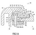
- FIGS. 1 a and 1 bAn exemplary version of a substrate ring assembly 20 that can be used to cover or protect at least a portion of a substrate support 22 in a substrate processing environment, is shown in FIGS. 1 a and 1 b .
- the substrate support 22which may comprise for example an electrostatic chuck 23 , has a substrate receiving surface 24 that receives and supports a substrate 104 during processing.
- the substrate ring assembly 20is provided to protect at least a portion of the support 22 by covering at least a portion of the support 22 .
- the substrate ring assembly 20comprises an annular band 26 having an inner perimeter 28 that is adapted to surround a periphery of the substrate 104 and the substrate receiving surface 24 .
- the inner perimeter 28also surrounds the substrate receiving surface 24 of the support 22 , and the annular band 26 protects regions of the support 22 that are not covered by the substrate 104 during processing.
- the annular band 26may surround and at least partially cover a peripheral edge 30 of the support 22 that would otherwise be exposed to the processing environment.
- the substrate ring assembly 20comprises an annular band 26 having a top portion 32 that extends over the peripheral edge 30 of the support 22 to protect the peripheral edge 30 , and a bottom portion 35 that extends downwardly and adjacent to the side of the peripheral edge 30 .
- the annular band 26can protect the covered surfaces of the support from, for example, erosion by energized process gases or the excessive deposition of process residues on these surfaces.
- the substrate ring assembly 20comprises a clamp 34 that clamps a portion of the annular band 26 to the substrate support 22 .
- Clamping of the annular band 26 to the support 22provides improved processing results at least in part because better heat exchange can occur between the clamped band 26 and the support 22 .
- Portions of the annular band 26can become excessively heated during substrate processing, such as for example the top surface 36 of the annular band 26 that is exposed to energized plasma of process gas. Excessive heating of the top surface 36 can lead to a thermal expansion mismatch between the annular band 26 and any process residues deposited on the top surface 36 of the band 26 , which can cause the process residues to flake away from the top surface 36 and potentially contaminate the substrate 104 .
- Clamping of the annular band 26 to the support 22also allows better heat exchange between the band 26 and the support 22 , to improve the temperature control of the annular band 26 .
- the support 22may be temperature controlled, for example, by providing a temperature controlled cooling plate 127 comprising cooling conduits 123 in the support 22 , as shown for example in FIG. 3 , allowing for good cooling of the clamped annular band 26 .
- Clamping of the annular band 26 against the support 22can also provide more secure coverage and protection of the support 22 .
- the improved temperature control of the band 26also allows for fabrication of the band out of more erosion resistant metal materials, such as for example, stainless steel, titanium or aluminum.
- FIGS. 1 a and 1 bOne embodiment of a substrate ring assembly 20 comprising a clamp 34 is shown in FIGS. 1 a and 1 b .
- the annular band 26comprises at least one opening 38 that extends therethrough, such as for example a substantially vertical opening extending from the top surface 36 of the annular band 26 to a bottom surface 42 of the band.
- the clamp 34comprises a fastener 40 that is shaped and sized to pass through the opening 38 to fasten the annular band to the support 22 .
- the clamp 34further comprises a bracket 44 that is adapted to receive the fastener 40 and secure the annular band 26 to the support 22 .
- the bracket 44can be braced against or otherwise connected to the substrate support 22 to clamp the annular band 26 against the support 22 .
- the bracket 44may comprise a clamping surface 46 that is pressed against a surface of the support 22 , such as the bottom surface 48 of the peripheral edge 30 , to clamp the annular band 26 against the support 22 , as shown for example in FIGS. 1 a and 1 b .
- the clamping surface 46may also press against the bottom surface 42 of the annular band 26 .
- the fastener 40comprises a structure suitable for passing through the opening 38 in the annular band 26 and connecting to the bracket 44 , such as for example at least one of a screw, clip, spring or other connector structure.
- the fastener 40can comprise a threaded screw that fits through the opening 38 in the annular band 26 and at least partially through an opening 39 in the bracket 44 , and where the opening 39 of the bracket 44 comprises complimentary threading that allows the bracket 44 to be tightened against the support 22 upon turning the screw.
- a desired number of openings 38 and fasteners 40can be provided to secure the annular band 26 to the support 22 .
- the support ring assembly 20can comprise from about 3 to about 24 openings 38 , such as about 8 openings 38 , that are placed in a desired configuration about the annular band 26 .
- the openings 38are positioned towards a periphery 50 of the annular band 26 .
- the openings 38extend through the top and bottom portions 32 , 42 of the annular band 26 to clamp the band 26 to the substrate support 22 .
- the bracket 44may comprise features that enable the bracket to “lock” on to the annular band 26 to better secure the band 26 .
- the bracket 44can comprise a raised wall 59 that is adapted to press against a peripheral sidewall 63 of the annular band, to lock the annular band into a desired clamped position.
- the clamp 34comprises a swiveling fastener 41 that is adapted to rotate the bracket 44 into a desired position to clamp the annular band 26 against the support 22 , as shown for example in FIG. 1 c .
- the swiveling fastener 41can comprise a swivel nut 43 that allows the bracket 44 to be rotated into place against the support 22 .
- the swiveling fastener 41may allow the bracket 44 to rotate about the axis 45 of the fastener 41 by turning the swiveling fastener 41 , such that for example the bracket can be rotated into or away from the clamping position by simply rotating the fastener 41 , for example by turning the top 47 of the fastener 41 .
- the swiveling fastener 41allows ready removal of the substrate ring assembly 20 , for example for cleaning of the assembly, substantially without requiring removal of the fastener 41 from the bracket 44 , and even substantially without requiring access to a portion of the ring assembly 20 or other element below the peripheral edge 30 of the support 22 .
- the top surface 36 of the annular bandcomprises a textured surface that is adapted to reduce the deposition of process deposits on undesired areas of the support 22 and support assembly 20 .
- the top surface 36desirably comprises features 52 that are shaped, sized and positioned to reduce the deposition of process residues on at least a portion of the surface 36 .
- the top surface 36may inhibit a flow or migration of process residues towards one or more openings 38 in the annular band at a periphery 50 of the annular band.
- the top surface 36may collect process residues in depressions in the surface 36 , and inhibit the migration of these residues towards the substrate 104 to reduce contamination of the substrate 104 .
- the top surface 36comprises at least one feature 52 comprising a protrusion 51 that is sized and shaped, as well as positioned on the top surface 36 , to reduce the flow or migration of process residues towards the substrate.
- the protrusion 51may comprise, for example, a raised ring or other feature 52 , that may be formed on the surface 36 .
- Textured features 52 on the surface 36can also comprise, for example, one or more grooves 53 or other depressions in the surface 36 .
- the textured features 52can be formed by methods know to those of ordinary skill in the art, such as for example by at least one of machining, knurling, or etching the features 52 into the top surface 36 .
- Embodiments of surfaces having textured featuresare described in, for example, U.S. patent application Ser. No. 10,880,235 to Tsai et al, assigned to Applied Materials, Inc, and filed on Jun. 28, 2004, which is herein incorporated by reference in its entirety.
- the ring assembly 20comprises a foot 54 that extends downwardly from the annular band 26 to press against the substrate support 22 .
- the foot 54is desirably shaped and sized to press against the substrate support 20 substantially without inducing cracks or fractures in the support 20 , and thus provides an improved structure for bracing the band 26 against the support.
- the foot 54may comprise a substantially vertical post that extend downwardly from the top portion 32 of the annular band 26 to press against a top surface 56 of the peripheral edge 30 .
- the foot 54desirably exerts substantially only a compressive stress on the peripheral edge 30 of the support 20 , and substantially no shearing or other horizontally directed stress that could induce cracking or fracturing of the peripheral ledge.
- the foot 54is also desirably positioned such that it substantially does not press against a top corner 58 a on the peripheral edge 30 or other part of the edge 30 that may be susceptible to cracking or chipping.
- the foot 54contacts substantially only the top surface 56 of the peripheral edge 30 , and does not cover more than about 70% of this peripheral edge surface 56 .
- the annular band 26desirably also comprises recessed surface regions 60 about the downwardly extending foot 54 that substantially do not contact the peripheral edge 30 of the support 22 , to reduce the stress of the band 26 on the peripheral edge 30 of the support 22 .
- one or more of the recessed regions 60may be about a top corner 58 a of the peripheral edge 30 , to reduce the amount of stress exerted on the top corner 58 a .
- Other parts of the substrate ring assembly 20may also be adapted to reduce the amount of pressure and/or stress exerted on the peripheral edge 30 of the support 22 .
- the bracket 44may comprise a raised lip 62 that presses against the peripheral edge 30 with substantially only a compressive force, and an adjacent recess 64 about a bottom corner 58 b of the peripheral edge to reduce pressure on the bottom corner 58 b .
- the bracket 44 and annular band foot 54may also be complementarily positioned such that the clamping force of one against the peripheral edge 30 is at least partially counteracted by the other.
- the bracket 44may press against the peripheral edge 30 substantially directly below where the foot 54 presses, so the force on the peripheral edge 30 is substantially equal above and below the peripheral edge 30 .
- the substrate ring assembly 20is adapted to reduce cracking or fracturing of the substrate support 22 by exerting substantially only a vertical, compressive stress on the peripheral edge 30 of the support, and substantially without pressing against portions of the support 22 that are readily cracked or chipped, such as corners 58 a,b of the peripheral edge 30 .
- the substrate ring assembly 20comprises a cover ring 70 that at least partially surrounds and at least partially covers a periphery 50 of the annular band 26 , as shown for example in FIGS. 1 a,b and c .
- the cover ring 70comprises a radially inwardly extending ledge 72 that extends across at least a portion of the annular band 26 to cover and protect portions of the band 26 .
- the cover ring 70comprises a downwardly extending protrusion 74 that is sized and shaped to inhibit the deposition of process deposits on at least a portion of the top surface 36 of the annular band 26 , for example to inhibit the flow of at least one of process gas and process deposits over the surface 36 .
- the protrusion 74may comprise, for example, an annular lip 78 at the inner diameter 79 of the inwardly extending ledge 72 , that extends downwards about 2 mm to about 5 mm from a bottom surface 76 of the cover ring 70 .
- the protrusion 74is sized, shaped, and positioned such that the protrusion 74 complements a textured top surface 36 of the annular band 26 .
- the protrusion 74may extend downwardly and adjacent to a raised protrusion 51 arising from the top surface 36 of the annular band 26 , to form a convoluted and constricted flow path 75 between the cover ring 70 and annular band 26 that inhibits the flow of process deposits past the protrusion 74 .
- the protrusion 74may even extend into a depressed feature such as a groove 53 in the top surface 36 of the band 26 , to further block a flow or migration of process deposits across the surface 26 .
- the cover ring 70is preferably fabricated of an erosion resistant material, which may be a metallic material such as for example at least one of stainless steel and titanium.
- the cover ring 70may also be fabricated of a ceramic material, such as for example aluminum oxide.
- the cover ring 70may also comprise a textured top surface to which process residues may adhere.
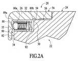
- the substrate ring assembly 20comprises a clamp 34 having a spring 80 to hold the annular band 26 against the substrate support 22 , as shown for example in FIGS. 2 a and 2 b .
- the clamp 34comprises a radial spring 80 a that is adapted to be compressed between the annular band 26 and the support 22 , such as for example a coil spring.
- the radial spring 80 acan be compressed between an interior surface 82 of the bottom portion 35 of the annular band 26 , and a sidewall 84 of the peripheral edge 30 of the support 22 .
- the radial spring 80 ais also supported underneath by a support ledge 86 that extends past the peripheral edge 30 .
- the compressed radial spring 80 aexerts a force on the annular band 26 and support 22 that resists slipping and other movements of the annular band 26 to secure the band 26 in place.
- the clamp 34can also comprise a ball bearing 88 at one or more ends 89 a,b of the radial spring 80 a,b to exert a compressional force to secure the annular band 26 .
- the ball bearingmay be at a first end 89 a of the spring 80 a that contacts the annular band 26 , to increase the clamp surface area that contacts the band 26 .
- the ball bearing 88can also ease removal of the annular band 26 , for example to allow cleaning of the band 26 , by allowing the band to “roll” off of the support 22 when a steady force is exerted upwardly on the band 26 .
- a second end 89 b of the radial spring 80 amay comprise a compression plate 92 having a surface area that is adapted to press against the peripheral edge 30 of the support 22 , to provide a greater surface area for the compression clamping.
- the annular band 26may also comprise a raised ridge 90 or bump on the interior surface 82 that is positioned below the radial spring 80 a when the annular band 26 is secured on the support 22 .
- the raised ridge 90increases the force required to move the band 26 upwardly by increasing the spring contraction distance that is necessary to roll the ball-bearing over the ridge 90 .
- the raised ridge 90 and radial spring clamp 34secure the annular band 26 to the support 22 during processing, while also allowing for efficient removal of the band 26 by applying a sufficient lift-off pressure.
- the clamp 34comprises a spring 80 b that is adapted to be extended between the annular band 26 and a portion of the support 22 to hold the band 26 on the support 22 , as shown for example in FIG. 2 b .
- the spring 80 bmay be vertically, radially, or otherwise extended according to the desired support configuration.
- the spring 80 bcomprises a first end 94 a that attaches to a portion of the annular band 26 , such as for example a cleft 96 in the bottom portion 35 of the annular band 26 .
- the cleft 96may be shaped and sized to provide a hook 98 on the annular band 26 that secures the first end 94 a of the spring 80 b .
- the first end 94 a of the spring 80 bcan also be attached to the annular band 26 by other means that are known to those of ordinary skill in the art.
- the support 22may comprise a support ledge 86 that extends past the peripheral edge 30 to support the annular band 26 from underneath.
- a second end 94 b of the spring 80 bis extended to attach to a clamping portion 99 of the support 22 .
- the spring 80 bis stretched between the annular band 26 and the clamping portion 99 of the support 22 to pull the annular band 26 against the support 22 .
- the second end 94 b of the spring 80 bcan be attached by hooking onto the clamping portion 99 of the support 22 .
- the second end 94 b of the spring 80 bis attached by means that substantially fixes the second end 94 b to the support 22 , for example by wrapping the second end 94 b about an attachment rod 97 on the support 22 , and the first end 94 a is detachably secured to the band 26 , as shown in FIG. 2 b .
- the second end 94 bmay be fixed onto the support 22 such that the first end 94 a of the spring 80 b can be rotated into place and stretched over the hook 98 on the annular band 26 to secure the annular band 26 onto the support 22 .
- the spring 80 bmay be substantially fixed onto the annular band 26 , and may be detachably secured to the support 22 during substrate processing.
- the spring 80 b that is extended between the annular band 26 and support 22comprises a latch clip, which may comprise a bent strip of metal with high spring constant that is sufficiently high to resist straightening of the strip, and thus exerts a force on the band 26 towards the support 22 .
- the spring 80 bcomprises a coil spring that is extended between the band 26 and support 22 .
- FIG. 3An example of a suitable process chamber 106 having the substrate ring assembly with the annular band 26 on the support 22 is shown in FIG. 3 .
- the chamber 106can be a part of a multi-chamber platform (not shown) having a cluster of interconnected chambers connected by a robot arm mechanism that transfers substrates 104 between the chambers 106 .
- the process chamber 106comprises a sputter deposition chamber, also called a physical vapor deposition or PVD chamber, which is capable of sputter depositing material on a substrate 104 , such as one or more of tantalum, tantalum nitride, titanium, titanium nitride, copper, tungsten, tungsten nitride and aluminum.
- the chamber 106comprises enclosure walls 118 that enclose a process zone 109 , and that include sidewalls 164 , a bottom wall 166 , and a ceiling 168 .
- a support ring 130can be arranged between the sidewalls 164 and ceiling 168 to support the ceiling 168 .
- Other chamber wallscan include one or more shields 120 that shield the enclosure walls 118 from the sputtering environment.
- the chamber 106comprises a substrate support 22 to support the substrate 104 in the sputter deposition chamber 106 .
- the substrate support 22may be electrically floating or may comprise an electrode 170 that is biased by a power supply 172 , such as an RF power supply.
- the substrate support 22can also comprise a moveable shutter disk 133 that can protect the upper surface 134 of the support 22 when the substrate 104 is not present.
- the substrate 104is introduced into the chamber 106 through a substrate loading inlet (not shown) in a sidewall 164 of the chamber 106 and placed on the support 22 .
- the support 22can be lifted or lowered by support lift bellows and a lift finger assembly (not shown) can be used to lift and lower the substrate onto the support 22 during transport of the substrate 104 into and out of the chamber 106 .
- the chamber 106can further comprise a temperature control system 119 to control one or more temperatures in the chamber 106 , such as a temperature of the support 22 .
- the temperature control system 119comprises a fluid supply adapted to provide heat exchange fluid to the support 22 from a fluid source 121 .
- One or more conduits 123deliver the heat exchange fluid from the fluid source 121 to the support 22 .
- the support 22can comprise one or more channels 125 therein, such as for example channels 125 in a metal cooling plate 127 , through which the heat exchange fluid is flowed to exchange heat with the support 22 and control the temperature of the support 22 , for example by heating or cooling the support 22 .
- a suitable heat exchange fluidmay be, for example, water.
- Controlling the temperature of the support 22can also provide good temperature of elements that are in good thermal contact with the support 22 , such as for example a substrate 104 on the surface 134 of the support 22 , and also a clamped portion of a substrate ring assembly 20 .
- the support 22may also comprise the substrate ring assembly 20 comprising one or more rings, such as the cover ring 70 and the annular band 26 , which may be called a deposition ring, and which cover at least a portion of the upper surface 134 of the support 22 , and such as a portion of the peripheral edge 30 of the support 22 , to inhibit erosion of the support 22 .
- the annular band 26at least partially surrounds the substrate 104 to protect portions of the support 22 not covered by the substrate 104 .
- the cover ring 70encircles and covers at least a portion of the annular band 26 , and reduces the deposition of particles onto both the annular band 26 and the underlying support 22 .
- the substrate ring assembly 20further comprises a clamp 34 to clamp the annular band 26 onto the substrate support 22 .
- a process gassuch as a sputtering gas
- a gas delivery system 112that includes a process gas supply comprising one or more gas sources 174 that each feed a conduit 176 having a gas flow control valve 178 , such as a mass flow controller, to pass a set flow rate of the gas therethrough.
- the conduits 176can feed the gases to a mixing manifold (not shown) in which the gases are mixed to from a desired process gas composition.
- the mixing manifoldfeeds a gas distributor 180 having one or more gas outlets 182 in the chamber 106 .
- the process gasmay comprise a non-reactive gas, such as argon or xenon, which is capable of energetically impinging upon and sputtering material from a target.
- the process gasmay also comprise a reactive gas, such as one or more of an oxygen-containing gas and a nitrogen-containing gas, that are capable of reacting with the sputtered material to form a layer on the substrate 104 .
- Spent process gas and byproductsare exhausted from the chamber 106 through an exhaust 122 which includes one or more exhaust ports 184 that receive spent process gas and pass the spent gas to an exhaust conduit 186 in which there is a throttle valve 188 to control the pressure of the gas in the chamber 106 .
- the exhaust conduit 186feeds one or more exhaust pumps 190 .
- the pressure of the sputtering gas in the chamber 106is set to sub-atmospheric levels.
- the sputtering chamber 106further comprises a sputtering target 124 facing a surface 105 of the substrate 104 , and comprising material to be sputtered onto the substrate 104 , such as for example at least one of tantalum and tantalum nitride.
- the target 124is electrically isolated from the chamber 106 by an annular insulator ring 132 , and is connected to a power supply 192 .
- the sputtering chamber 106also has a shield 120 to protect a wall 118 of the chamber 106 from sputtered material.
- the shield 120can comprise a wall-like cylindrical shape having upper and lower shield sections 120 a , 120 b that shield the upper and lower regions of the chamber 106 . In the version shown in FIG.
- the shield 120has an upper section 120 a mounted to the support ring 130 and a lower section 120 b that is fitted to the cover ring 70 .
- a clamp shield 141comprising a clamping ring can also be provided to clamp the upper and lower shield sections 120 a,b together.
- Alternative shield configurationssuch as inner and outer shields, can also be provided.
- one or more of the power supply 192 , target 124 , and shield 120operate as a gas energizer 116 that is capable of energizing the sputtering gas to sputter material from the target 124 .
- the power supply 192applies a bias voltage to the target 124 with respect to the shield 120 .
- the electric field generated in the chamber 106 from the applied voltageenergizes the sputtering gas to form a plasma that energetically impinges upon and bombards the target 124 to sputter material off the target 124 and onto the substrate 104 .
- the support 22 having the electrode 170 and support electrode power supply 172may also operate as part of the gas energizer 116 by energizing and accelerating ionized material sputtered from the target 124 towards the substrate 104 .
- a gas energizing coil 135can be provided that is powered by a power supply 192 and that is positioned within the chamber 106 to provide enhanced energized gas characteristics, such as improved energized gas density.
- the gas energizing coil 135can be supported by a coil support 137 that is attached to a shield 120 or other wall in the chamber 106 .
- the chamber 106can be controlled by a controller 194 that comprises program code having instruction sets to operate components of the chamber 106 to process substrates 104 in the chamber 106 .
- the controller 194can comprise a substrate positioning instruction set to operate one or more of the substrate support 22 and substrate transport to position a substrate 104 in the chamber 106 ; a gas flow control instruction set to operate the flow control valves 178 to set a flow of sputtering gas to the chamber 106 ; a gas pressure control instruction set to operate the exhaust throttle valve 188 to maintain a pressure in the chamber 106 ; a gas energizer control instruction set to operate the gas energizer 116 to set a gas energizing power level; a temperature control instruction set to control a temperature control system 119 to control temperatures in the chamber 106 ; and a process monitoring instruction set to monitor the process in the chamber 106 .
- the substrate ring assembly 20comprising the clamp 34 and annular band 26 can be used in other types of applications, as would be apparent to one of ordinary skill, for example, etching, CVD and cleaning processed.
- Other configurations of the substrate ring assembly 20 and clamp 34can also be used.
- other methods and configurations for clamping and annular band 26 to a support 22can be provided. Therefore, the spirit and scope of the appended claims should not be limited to the description of the preferred versions contained herein.
Landscapes
- Engineering & Computer Science (AREA)
- Chemical & Material Sciences (AREA)
- Physics & Mathematics (AREA)
- Condensed Matter Physics & Semiconductors (AREA)
- General Physics & Mathematics (AREA)
- Manufacturing & Machinery (AREA)
- Computer Hardware Design (AREA)
- Microelectronics & Electronic Packaging (AREA)
- Power Engineering (AREA)
- Plasma & Fusion (AREA)
- Analytical Chemistry (AREA)
- Chemical Kinetics & Catalysis (AREA)
- Materials Engineering (AREA)
- Mechanical Engineering (AREA)
- Metallurgy (AREA)
- Organic Chemistry (AREA)
- Container, Conveyance, Adherence, Positioning, Of Wafer (AREA)
- Physical Vapour Deposition (AREA)
Abstract
Description
- Embodiments of the present invention relate to a support ring assembly to support a substrate in a process chamber.
- In the processing of substrates, such as semiconductor wafers and displays, a substrate is placed in a process chamber and exposed to an energized gas to deposit or etch material on the substrate. A typical process chamber comprises process components that include an enclosure wall that encloses a process zone, a gas supply to provide a gas in the chamber, a gas energizer to energize the process gas to process the substrate, a substrate support, and a gas exhaust. The process chamber components can also comprise a process kit, which typically includes one or more parts that can assist in securing and protecting the substrate during processing, such as for example, substrate rings which are rings that are located about the periphery of the substrate, such as deposition rings, cover rings and shadow rings.
- In physical vapor deposition (PVD) processes, a substrate ring comprising a deposition ring is provided about the periphery of the substrate. The deposition ring typically surrounds the substrate and has a lip or ledge that rests on the substrate support. The ring shields the sidewall surfaces and peripheral edge of the substrate support that would otherwise be exposed to the energized gas in the chamber, from deposition of process residues. Thus, the deposition ring reduces the accumulation of process residues on the support, which would eventually flake off and contaminate the substrate. The deposition ring can also reduce erosion of the support structure by the energized gas. Providing a deposition ring also lowers the frequency with which the support assembly requires cleaning, because deposition ring itself can be periodically removed from the chamber and cleaned, for example, with HF and HNO3, to remove process residues that accumulate on the ring during substrate process cycles.
- However, certain processes, such as for example, tantalum PVD processes with their exposure to the energized gas in the chamber during processing, heats up the deposition ring. Typically, the deposition rings, such as for example aluminum oxide deposition rings do not exchange a sufficient amount of heat with their surroundings in the vacuum environment to lower the temperature of the rings to acceptable levels. Excessive heating of the deposition ring is detrimental, because thermal stresses between the deposition ring and process residues accumulated on the ring, result in the peeling or spalling of the process residues from the deposition ring, and resultant contamination of the substrate. Also, the hot deposition ring can create temperature gradients emanating from the periphery of the substrate, which change the temperature of the substrate or energized gas during processing. Yet another problem with conventional rings, such as aluminum oxide deposition rings, is that they erode during cleaning and refurbishment processes, reducing their lifetime. This is especially true when cleaning process residues that are chemically difficult to remove, such as for example, tantalum deposits formed on aluminum oxide rings.
- Accordingly, it is desirable to have a substrate ring, such as a deposition ring, that does not excessively increase in temperature during the processing of substrates. It is furthermore desirable to have a substrate ring that is not excessively eroded during cleaning of the ring. It is furthermore desirable to have a substrate ring that can reduce the formation of excessively high temperature gradients during substrate processing.
- In one version, a substrate ring assembly is provided for a substrate support having a peripheral edge. The assembly has an annular band having an inner perimeter that surrounds and at least partially covers the peripheral edge of the substrate support. The assembly also has a clamp to secure the annular band to the peripheral edge of the substrate support.
- In another version, the substrate ring assembly has an annular band having an inner perimeter that at least partially surrounds and at least partially covers the peripheral edge of the substrate support. The annular band has at least one protrusion on a top surface of the annular band that is adapted to inhibit a flow of process gas over the top surface. A foot extends downwardly from the annular band, and is adapted to press against a surface of the substrate support.
- In another version, the substrate ring assembly has an annular band having an inner perimeter that surrounds and at least partially covers a peripheral edge of the substrate support, and a foot extending downwardly from the annular band. The foot is shaped, sized and positioned to allow the band, when the band is held against the substrate support, to exert substantially a compressive stress on the substrate support.
- These features, aspects and advantages of the present invention will become better understood with regard to the following description, appended claims, and accompanying drawings, which illustrate examples of the invention. However, it is to be understood that each of the features can be used in the invention in general, not merely in the context of the particular drawings, and the invention includes any combination of these features, where:
FIG. 1 ais a partial sectional side view of an embodiment of a substrate ring assembly having a clamped annular band;FIG. 1 bis a partial top view of an embodiment of a substrate support having the substrate ring assembly ofFIG. 1 a;FIG. 1 cis a partial sectional side view of an embodiment of the substrate ring assembly ofFIG. 1 ahaving a swiveling fastener;FIG. 2 ais a partial sectional side view of an embodiment of a substrate ring assembly having a clamp comprising a radial spring;FIG. 2 bis a partial sectional side view of an embodiment of a substrate ring assembly having a clamp comprising an extended spring; andFIG. 3 is a partial sectional side view of an embodiment of process chamber having a substrate ring assembly.- An exemplary version of a
substrate ring assembly 20 that can be used to cover or protect at least a portion of asubstrate support 22 in a substrate processing environment, is shown inFIGS. 1 aand1b. The substrate support22, which may comprise for example anelectrostatic chuck 23, has asubstrate receiving surface 24 that receives and supports asubstrate 104 during processing. Thesubstrate ring assembly 20 is provided to protect at least a portion of thesupport 22 by covering at least a portion of thesupport 22. Thesubstrate ring assembly 20 comprises anannular band 26 having aninner perimeter 28 that is adapted to surround a periphery of thesubstrate 104 and thesubstrate receiving surface 24. Theinner perimeter 28 also surrounds thesubstrate receiving surface 24 of thesupport 22, and theannular band 26 protects regions of thesupport 22 that are not covered by thesubstrate 104 during processing. For example, theannular band 26 may surround and at least partially cover aperipheral edge 30 of thesupport 22 that would otherwise be exposed to the processing environment. In the version shown inFIG. 1 a, thesubstrate ring assembly 20 comprises anannular band 26 having atop portion 32 that extends over theperipheral edge 30 of thesupport 22 to protect theperipheral edge 30, and abottom portion 35 that extends downwardly and adjacent to the side of theperipheral edge 30. Theannular band 26 can protect the covered surfaces of the support from, for example, erosion by energized process gases or the excessive deposition of process residues on these surfaces. - In one version, the
substrate ring assembly 20 comprises aclamp 34 that clamps a portion of theannular band 26 to thesubstrate support 22. Clamping of theannular band 26 to thesupport 22 provides improved processing results at least in part because better heat exchange can occur between theclamped band 26 and thesupport 22. Portions of theannular band 26 can become excessively heated during substrate processing, such as for example thetop surface 36 of theannular band 26 that is exposed to energized plasma of process gas. Excessive heating of thetop surface 36 can lead to a thermal expansion mismatch between theannular band 26 and any process residues deposited on thetop surface 36 of theband 26, which can cause the process residues to flake away from thetop surface 36 and potentially contaminate thesubstrate 104. Clamping of theannular band 26 to thesupport 22 also allows better heat exchange between theband 26 and thesupport 22, to improve the temperature control of theannular band 26. For example, thesupport 22 may be temperature controlled, for example, by providing a temperature controlledcooling plate 127 comprisingcooling conduits 123 in thesupport 22, as shown for example inFIG. 3 , allowing for good cooling of the clampedannular band 26. Clamping of theannular band 26 against thesupport 22 can also provide more secure coverage and protection of thesupport 22. The improved temperature control of theband 26 also allows for fabrication of the band out of more erosion resistant metal materials, such as for example, stainless steel, titanium or aluminum. - One embodiment of a
substrate ring assembly 20 comprising aclamp 34 is shown inFIGS. 1 aand1b. In this version, theannular band 26 comprises at least oneopening 38 that extends therethrough, such as for example a substantially vertical opening extending from thetop surface 36 of theannular band 26 to abottom surface 42 of the band. Theclamp 34 comprises afastener 40 that is shaped and sized to pass through theopening 38 to fasten the annular band to thesupport 22. In the version shown inFIG. 1 a, theclamp 34 further comprises abracket 44 that is adapted to receive thefastener 40 and secure theannular band 26 to thesupport 22. Thebracket 44 can be braced against or otherwise connected to thesubstrate support 22 to clamp theannular band 26 against thesupport 22. For example, thebracket 44 may comprise aclamping surface 46 that is pressed against a surface of thesupport 22, such as thebottom surface 48 of theperipheral edge 30, to clamp theannular band 26 against thesupport 22, as shown for example inFIGS. 1 aand1b. Theclamping surface 46 may also press against thebottom surface 42 of theannular band 26. - The
fastener 40 comprises a structure suitable for passing through theopening 38 in theannular band 26 and connecting to thebracket 44, such as for example at least one of a screw, clip, spring or other connector structure. For example, in one version, thefastener 40 can comprise a threaded screw that fits through theopening 38 in theannular band 26 and at least partially through anopening 39 in thebracket 44, and where theopening 39 of thebracket 44 comprises complimentary threading that allows thebracket 44 to be tightened against thesupport 22 upon turning the screw. Also, a desired number ofopenings 38 andfasteners 40 can be provided to secure theannular band 26 to thesupport 22. For example, thesupport ring assembly 20 can comprise from about 3 to about 24openings 38, such as about 8openings 38, that are placed in a desired configuration about theannular band 26. In the version shown inFIGS. 1 aand1b, theopenings 38 are positioned towards aperiphery 50 of theannular band 26. Theopenings 38 extend through the top andbottom portions annular band 26 to clamp theband 26 to thesubstrate support 22. Also, thebracket 44 may comprise features that enable the bracket to “lock” on to theannular band 26 to better secure theband 26. For example, thebracket 44 can comprise a raisedwall 59 that is adapted to press against aperipheral sidewall 63 of the annular band, to lock the annular band into a desired clamped position. - In yet another embodiment, the
clamp 34 comprises a swivelingfastener 41 that is adapted to rotate thebracket 44 into a desired position to clamp theannular band 26 against thesupport 22, as shown for example inFIG. 1 c. For example, the swivelingfastener 41 can comprise aswivel nut 43 that allows thebracket 44 to be rotated into place against thesupport 22. The swivelingfastener 41 may allow thebracket 44 to rotate about theaxis 45 of thefastener 41 by turning the swivelingfastener 41, such that for example the bracket can be rotated into or away from the clamping position by simply rotating thefastener 41, for example by turning the top47 of thefastener 41. Thus, the swivelingfastener 41 allows ready removal of thesubstrate ring assembly 20, for example for cleaning of the assembly, substantially without requiring removal of thefastener 41 from thebracket 44, and even substantially without requiring access to a portion of thering assembly 20 or other element below theperipheral edge 30 of thesupport 22. - In one version, the
top surface 36 of the annular band comprises a textured surface that is adapted to reduce the deposition of process deposits on undesired areas of thesupport 22 andsupport assembly 20. Thetop surface 36 desirably comprisesfeatures 52 that are shaped, sized and positioned to reduce the deposition of process residues on at least a portion of thesurface 36. For example, thetop surface 36 may inhibit a flow or migration of process residues towards one ormore openings 38 in the annular band at aperiphery 50 of the annular band. Thetop surface 36 may collect process residues in depressions in thesurface 36, and inhibit the migration of these residues towards thesubstrate 104 to reduce contamination of thesubstrate 104. In one version, thetop surface 36 comprises at least onefeature 52 comprising aprotrusion 51 that is sized and shaped, as well as positioned on thetop surface 36, to reduce the flow or migration of process residues towards the substrate. Theprotrusion 51 may comprise, for example, a raised ring orother feature 52, that may be formed on thesurface 36. Textured features52 on thesurface 36 can also comprise, for example, one ormore grooves 53 or other depressions in thesurface 36. The textured features52 can be formed by methods know to those of ordinary skill in the art, such as for example by at least one of machining, knurling, or etching thefeatures 52 into thetop surface 36. Embodiments of surfaces having textured features are described in, for example, U.S. patent application Ser. No. 10,880,235 to Tsai et al, assigned to Applied Materials, Inc, and filed on Jun. 28, 2004, which is herein incorporated by reference in its entirety. - In one embodiment, the
ring assembly 20 comprises afoot 54 that extends downwardly from theannular band 26 to press against thesubstrate support 22. Thefoot 54 is desirably shaped and sized to press against thesubstrate support 20 substantially without inducing cracks or fractures in thesupport 20, and thus provides an improved structure for bracing theband 26 against the support. For example, as shown inFIG. 1 a, thefoot 54 may comprise a substantially vertical post that extend downwardly from thetop portion 32 of theannular band 26 to press against atop surface 56 of theperipheral edge 30. Thefoot 54 desirably exerts substantially only a compressive stress on theperipheral edge 30 of thesupport 20, and substantially no shearing or other horizontally directed stress that could induce cracking or fracturing of the peripheral ledge. Thefoot 54 is also desirably positioned such that it substantially does not press against atop corner 58aon theperipheral edge 30 or other part of theedge 30 that may be susceptible to cracking or chipping. In one version, thefoot 54 contacts substantially only thetop surface 56 of theperipheral edge 30, and does not cover more than about 70% of thisperipheral edge surface 56. - The
annular band 26 desirably also comprises recessedsurface regions 60 about the downwardly extendingfoot 54 that substantially do not contact theperipheral edge 30 of thesupport 22, to reduce the stress of theband 26 on theperipheral edge 30 of thesupport 22. For example, one or more of the recessedregions 60 may be about atop corner 58aof theperipheral edge 30, to reduce the amount of stress exerted on thetop corner 58a. Other parts of thesubstrate ring assembly 20 may also be adapted to reduce the amount of pressure and/or stress exerted on theperipheral edge 30 of thesupport 22. For example, thebracket 44 may comprise a raisedlip 62 that presses against theperipheral edge 30 with substantially only a compressive force, and anadjacent recess 64 about abottom corner 58bof the peripheral edge to reduce pressure on thebottom corner 58b. Thebracket 44 andannular band foot 54 may also be complementarily positioned such that the clamping force of one against theperipheral edge 30 is at least partially counteracted by the other. For example, thebracket 44 may press against theperipheral edge 30 substantially directly below where thefoot 54 presses, so the force on theperipheral edge 30 is substantially equal above and below theperipheral edge 30. Thus, thesubstrate ring assembly 20 is adapted to reduce cracking or fracturing of thesubstrate support 22 by exerting substantially only a vertical, compressive stress on theperipheral edge 30 of the support, and substantially without pressing against portions of thesupport 22 that are readily cracked or chipped, such ascorners 58a,bof theperipheral edge 30. - In one version, the
substrate ring assembly 20 comprises acover ring 70 that at least partially surrounds and at least partially covers aperiphery 50 of theannular band 26, as shown for example inFIGS. 1 a,bandc. Thecover ring 70 comprises a radially inwardly extendingledge 72 that extends across at least a portion of theannular band 26 to cover and protect portions of theband 26. In one version, thecover ring 70 comprises a downwardly extendingprotrusion 74 that is sized and shaped to inhibit the deposition of process deposits on at least a portion of thetop surface 36 of theannular band 26, for example to inhibit the flow of at least one of process gas and process deposits over thesurface 36. Theprotrusion 74 may comprise, for example, anannular lip 78 at theinner diameter 79 of the inwardly extendingledge 72, that extends downwards about 2 mm to about 5 mm from abottom surface 76 of thecover ring 70. In one version, theprotrusion 74 is sized, shaped, and positioned such that theprotrusion 74 complements a texturedtop surface 36 of theannular band 26. For example, theprotrusion 74 may extend downwardly and adjacent to a raisedprotrusion 51 arising from thetop surface 36 of theannular band 26, to form a convoluted andconstricted flow path 75 between thecover ring 70 andannular band 26 that inhibits the flow of process deposits past theprotrusion 74. Theprotrusion 74 may even extend into a depressed feature such as agroove 53 in thetop surface 36 of theband 26, to further block a flow or migration of process deposits across thesurface 26. Thecover ring 70 is preferably fabricated of an erosion resistant material, which may be a metallic material such as for example at least one of stainless steel and titanium. Thecover ring 70 may also be fabricated of a ceramic material, such as for example aluminum oxide. Thecover ring 70 may also comprise a textured top surface to which process residues may adhere. - In yet another version, the
substrate ring assembly 20 comprises aclamp 34 having a spring80 to hold theannular band 26 against thesubstrate support 22, as shown for example inFIGS. 2 aand2b. In the version shown inFIG. 2 a, theclamp 34 comprises aradial spring 80athat is adapted to be compressed between theannular band 26 and thesupport 22, such as for example a coil spring. For example, theradial spring 80acan be compressed between aninterior surface 82 of thebottom portion 35 of theannular band 26, and a sidewall84 of theperipheral edge 30 of thesupport 22. In the version shown inFIG. 2 a, theradial spring 80ais also supported underneath by asupport ledge 86 that extends past theperipheral edge 30. The compressedradial spring 80aexerts a force on theannular band 26 andsupport 22 that resists slipping and other movements of theannular band 26 to secure theband 26 in place. - The
clamp 34 can also comprise aball bearing 88 at one or more ends89a,bof theradial spring 80a,bto exert a compressional force to secure theannular band 26. For example, the ball bearing may be at afirst end 89aof thespring 80athat contacts theannular band 26, to increase the clamp surface area that contacts theband 26. Theball bearing 88 can also ease removal of theannular band 26, for example to allow cleaning of theband 26, by allowing the band to “roll” off of thesupport 22 when a steady force is exerted upwardly on theband 26. Asecond end 89bof theradial spring 80amay comprise acompression plate 92 having a surface area that is adapted to press against theperipheral edge 30 of thesupport 22, to provide a greater surface area for the compression clamping. Theannular band 26 may also comprise a raisedridge 90 or bump on theinterior surface 82 that is positioned below theradial spring 80awhen theannular band 26 is secured on thesupport 22. The raisedridge 90 increases the force required to move theband 26 upwardly by increasing the spring contraction distance that is necessary to roll the ball-bearing over theridge 90. Thus, the raisedridge 90 andradial spring clamp 34 secure theannular band 26 to thesupport 22 during processing, while also allowing for efficient removal of theband 26 by applying a sufficient lift-off pressure. - In yet another version; the
clamp 34 comprises aspring 80bthat is adapted to be extended between theannular band 26 and a portion of thesupport 22 to hold theband 26 on thesupport 22, as shown for example inFIG. 2 b. Thespring 80bmay be vertically, radially, or otherwise extended according to the desired support configuration. In the version shown inFIG. 2 b, thespring 80bcomprises afirst end 94athat attaches to a portion of theannular band 26, such as for example a cleft96 in thebottom portion 35 of theannular band 26. For example, the cleft96 may be shaped and sized to provide ahook 98 on theannular band 26 that secures thefirst end 94aof thespring 80b. Thefirst end 94aof thespring 80bcan also be attached to theannular band 26 by other means that are known to those of ordinary skill in the art. Thesupport 22 may comprise asupport ledge 86 that extends past theperipheral edge 30 to support theannular band 26 from underneath. Asecond end 94bof thespring 80bis extended to attach to a clampingportion 99 of thesupport 22. Thus, thespring 80bis stretched between theannular band 26 and the clampingportion 99 of thesupport 22 to pull theannular band 26 against thesupport 22. Thesecond end 94bof thespring 80bcan be attached by hooking onto the clampingportion 99 of thesupport 22. - In one version, the
second end 94bof thespring 80bis attached by means that substantially fixes thesecond end 94bto thesupport 22, for example by wrapping thesecond end 94babout anattachment rod 97 on thesupport 22, and thefirst end 94ais detachably secured to theband 26, as shown inFIG. 2 b. For example, thesecond end 94bmay be fixed onto thesupport 22 such that thefirst end 94aof thespring 80bcan be rotated into place and stretched over thehook 98 on theannular band 26 to secure theannular band 26 onto thesupport 22. To remove theannular band 26, thefirst end 94ais lifted up and over thehook 98 and pulled away from theband 26 to release theband 26 from thesupport 22. Alternatively, thespring 80bmay be substantially fixed onto theannular band 26, and may be detachably secured to thesupport 22 during substrate processing. In one version, thespring 80bthat is extended between theannular band 26 andsupport 22 comprises a latch clip, which may comprise a bent strip of metal with high spring constant that is sufficiently high to resist straightening of the strip, and thus exerts a force on theband 26 towards thesupport 22. In another version, thespring 80bcomprises a coil spring that is extended between theband 26 andsupport 22. - An example of a
suitable process chamber 106 having the substrate ring assembly with theannular band 26 on thesupport 22 is shown inFIG. 3 . Thechamber 106 can be a part of a multi-chamber platform (not shown) having a cluster of interconnected chambers connected by a robot arm mechanism that transferssubstrates 104 between thechambers 106. In the version shown, theprocess chamber 106 comprises a sputter deposition chamber, also called a physical vapor deposition or PVD chamber, which is capable of sputter depositing material on asubstrate 104, such as one or more of tantalum, tantalum nitride, titanium, titanium nitride, copper, tungsten, tungsten nitride and aluminum. Thechamber 106 comprisesenclosure walls 118 that enclose aprocess zone 109, and that includesidewalls 164, abottom wall 166, and aceiling 168. A support ring130 can be arranged between thesidewalls 164 andceiling 168 to support theceiling 168. Other chamber walls can include one ormore shields 120 that shield theenclosure walls 118 from the sputtering environment. - The
chamber 106 comprises asubstrate support 22 to support thesubstrate 104 in thesputter deposition chamber 106. Thesubstrate support 22 may be electrically floating or may comprise anelectrode 170 that is biased by apower supply 172, such as an RF power supply. Thesubstrate support 22 can also comprise amoveable shutter disk 133 that can protect theupper surface 134 of thesupport 22 when thesubstrate 104 is not present. In operation, thesubstrate 104 is introduced into thechamber 106 through a substrate loading inlet (not shown) in asidewall 164 of thechamber 106 and placed on thesupport 22. Thesupport 22 can be lifted or lowered by support lift bellows and a lift finger assembly (not shown) can be used to lift and lower the substrate onto thesupport 22 during transport of thesubstrate 104 into and out of thechamber 106. - The
chamber 106 can further comprise atemperature control system 119 to control one or more temperatures in thechamber 106, such as a temperature of thesupport 22. In one version, thetemperature control system 119 comprises a fluid supply adapted to provide heat exchange fluid to thesupport 22 from afluid source 121. One ormore conduits 123 deliver the heat exchange fluid from thefluid source 121 to thesupport 22. Thesupport 22 can comprise one ormore channels 125 therein, such as forexample channels 125 in ametal cooling plate 127, through which the heat exchange fluid is flowed to exchange heat with thesupport 22 and control the temperature of thesupport 22, for example by heating or cooling thesupport 22. A suitable heat exchange fluid may be, for example, water. Controlling the temperature of thesupport 22 can also provide good temperature of elements that are in good thermal contact with thesupport 22, such as for example asubstrate 104 on thesurface 134 of thesupport 22, and also a clamped portion of asubstrate ring assembly 20. - The
support 22 may also comprise thesubstrate ring assembly 20 comprising one or more rings, such as thecover ring 70 and theannular band 26, which may be called a deposition ring, and which cover at least a portion of theupper surface 134 of thesupport 22, and such as a portion of theperipheral edge 30 of thesupport 22, to inhibit erosion of thesupport 22. Theannular band 26 at least partially surrounds thesubstrate 104 to protect portions of thesupport 22 not covered by thesubstrate 104. Thecover ring 70 encircles and covers at least a portion of theannular band 26, and reduces the deposition of particles onto both theannular band 26 and theunderlying support 22. Thesubstrate ring assembly 20 further comprises aclamp 34 to clamp theannular band 26 onto thesubstrate support 22. - A process gas, such as a sputtering gas, is introduced into the
chamber 106 through agas delivery system 112 that includes a process gas supply comprising one ormore gas sources 174 that each feed aconduit 176 having a gasflow control valve 178, such as a mass flow controller, to pass a set flow rate of the gas therethrough. Theconduits 176 can feed the gases to a mixing manifold (not shown) in which the gases are mixed to from a desired process gas composition. The mixing manifold feeds agas distributor 180 having one ormore gas outlets 182 in thechamber 106. The process gas may comprise a non-reactive gas, such as argon or xenon, which is capable of energetically impinging upon and sputtering material from a target. The process gas may also comprise a reactive gas, such as one or more of an oxygen-containing gas and a nitrogen-containing gas, that are capable of reacting with the sputtered material to form a layer on thesubstrate 104. Spent process gas and byproducts are exhausted from thechamber 106 through anexhaust 122 which includes one or moreexhaust ports 184 that receive spent process gas and pass the spent gas to anexhaust conduit 186 in which there is athrottle valve 188 to control the pressure of the gas in thechamber 106. Theexhaust conduit 186 feeds one or more exhaust pumps190. Typically, the pressure of the sputtering gas in thechamber 106 is set to sub-atmospheric levels. - The sputtering
chamber 106 further comprises asputtering target 124 facing asurface 105 of thesubstrate 104, and comprising material to be sputtered onto thesubstrate 104, such as for example at least one of tantalum and tantalum nitride. Thetarget 124 is electrically isolated from thechamber 106 by anannular insulator ring 132, and is connected to apower supply 192. The sputteringchamber 106 also has ashield 120 to protect awall 118 of thechamber 106 from sputtered material. Theshield 120 can comprise a wall-like cylindrical shape having upper andlower shield sections chamber 106. In the version shown inFIG. 3 , theshield 120 has anupper section 120amounted to the support ring130 and alower section 120bthat is fitted to thecover ring 70. Aclamp shield 141 comprising a clamping ring can also be provided to clamp the upper andlower shield sections 120a,btogether. Alternative shield configurations, such as inner and outer shields, can also be provided. In one version, one or more of thepower supply 192,target 124, and shield120, operate as agas energizer 116 that is capable of energizing the sputtering gas to sputter material from thetarget 124. Thepower supply 192 applies a bias voltage to thetarget 124 with respect to theshield 120. The electric field generated in thechamber 106 from the applied voltage energizes the sputtering gas to form a plasma that energetically impinges upon and bombards thetarget 124 to sputter material off thetarget 124 and onto thesubstrate 104. Thesupport 22 having theelectrode 170 and supportelectrode power supply 172 may also operate as part of thegas energizer 116 by energizing and accelerating ionized material sputtered from thetarget 124 towards thesubstrate 104. Furthermore, agas energizing coil 135 can be provided that is powered by apower supply 192 and that is positioned within thechamber 106 to provide enhanced energized gas characteristics, such as improved energized gas density. Thegas energizing coil 135 can be supported by acoil support 137 that is attached to ashield 120 or other wall in thechamber 106. - The
chamber 106 can be controlled by acontroller 194 that comprises program code having instruction sets to operate components of thechamber 106 to processsubstrates 104 in thechamber 106. For example, thecontroller 194 can comprise a substrate positioning instruction set to operate one or more of thesubstrate support 22 and substrate transport to position asubstrate 104 in thechamber 106; a gas flow control instruction set to operate theflow control valves 178 to set a flow of sputtering gas to thechamber 106; a gas pressure control instruction set to operate theexhaust throttle valve 188 to maintain a pressure in thechamber 106; a gas energizer control instruction set to operate thegas energizer 116 to set a gas energizing power level; a temperature control instruction set to control atemperature control system 119 to control temperatures in thechamber 106; and a process monitoring instruction set to monitor the process in thechamber 106. - The present invention has been described with reference to certain preferred versions thereof; however, other versions are possible. For example, the
substrate ring assembly 20 comprising theclamp 34 andannular band 26 can be used in other types of applications, as would be apparent to one of ordinary skill, for example, etching, CVD and cleaning processed. Other configurations of thesubstrate ring assembly 20 and clamp34 can also be used. For example, other methods and configurations for clamping andannular band 26 to asupport 22 can be provided. Therefore, the spirit and scope of the appended claims should not be limited to the description of the preferred versions contained herein.
Claims (20)
1. A substrate ring assembly for a substrate support having a peripheral edge, the assembly comprising:
(a) an annular band having an inner perimeter that surrounds and at least partially covers the peripheral edge of the substrate support; and
(b) a clamp to secure the annular band to the peripheral edge of the substrate support.
2. An assembly according toclaim 1 further comprising a foot that extends downwardly from the annular band to press against the substrate support.
3. An assembly according toclaim 1 wherein the annular band comprises a top surface having at least one protrusion that is sized and shaped to reduce the deposition of process deposits on at least a portion of the top surface.
4. An assembly according toclaim 1 wherein the band comprises at least one substantially vertical opening therethrough, and wherein the clamp comprises (i) at least one fastener adapted to pass through the opening in the band, and (ii) a bracket that is adapted receive the fastener and secure the annular band to the support.
5. An assembly according toclaim 4 wherein the fastener comprises a swiveling fastener that is capable of rotating the bracket to brace the bracket against the support.
6. An assembly according toclaim 4 further comprising a cover ring that surrounds a periphery of the annular band and has a ledge that extends inwardly over the annular band periphery, the ledge comprising a downwardly extending protrusion that is sized and shaped to reduce the deposition of process deposits on at least a portion of the top surface.
7. An assembly according toclaim 1 wherein the clamp comprises a radial spring that is compressed between the interior of the annular band and the peripheral edge of the support to hold the annular band against the support.
8. An assembly according toclaim 1 wherein the clamp comprises a spring that is adapted to be extended between the annular band and a portion of the substrate support to hold the annular band against the peripheral edge of the support.
9. An assembly according toclaim 1 wherein the support ring comprises at least one of stainless steel, titanium and aluminum.
10. A substrate processing chamber comprising the support ring assembly ofclaim 1 , and further comprising a substrate support, gas delivery system, gas energizer and gas exhaust.
11. A substrate ring assembly for a substrate support having a peripheral edge, the assembly comprising:
(a) an annular band having an inner perimeter that at least partially surrounds and at least partially covers the peripheral edge of the substrate support, the annular band comprising at least one protrusion on a top surface of the annular band, the protrusion being adapted to inhibit the deposition of process deposit on at least a portion of the top surface; and
(b) a foot extending downwardly from the annular band, the foot being adapted to press against a surface of the substrate support.
12. An assembly according toclaim 11 further comprising a clamp comprising at least one fastener adapted to pass through a vertical opening in the annular band, and further comprising a bracket to receive the fastener and secure the annular band to the support.
13. An assembly according toclaim 12 wherein the fastener comprises a swiveling fastener that is capable of rotating the bracket to brace the bracket against the support.
14. An assembly according toclaim 11 further comprising a cover ring that surrounds a periphery of the annular band and has a ledge that extends inwardly over the annular band periphery, the ledge comprising a downwardly extending protrusion that is sized and shaped to reduce the deposition of process deposits on at least a portion of the top surface of the annular band.
15. An assembly according toclaim 11 wherein the annular band comprises a downwardly extending foot that is shaped and sized to press against the peripheral edge of the substrate support substantially without inducing cracks in the peripheral edge.
16. An assembly according toclaim 15 wherein the annular band comprises recessed surface regions about the downwardly extending foot that substantially do not contact the peripheral edge.
17. A substrate ring assembly for a substrate support having a peripheral edge, the assembly comprising:
(a) an annular band having an inner perimeter that surrounds and at least partially covers a peripheral edge of the substrate support; and
(b) a foot extending downwardly from the annular band, the foot being shaped, sized and position to allow the band, when the band is held against the substrate support, to exert substantially only a compressive stress on the substrate support.
18. An assembly according toclaim 17 wherein the foot is configured such that substantially no horizontal force is exerted on the substrate support when the band is held against the support.
19. An assembly according toclaim 17 wherein the annular band comprises recessed surface regions about the foot that substantially do not contact the peripheral edge of the support.
20. An assembly according toclaim 19 wherein at least one recessed region is shaped, sized and positioned about a top corner of the support peripheral edge, such that the top corner substantially does not contact the annular band.
Priority Applications (5)
| Application Number | Priority Date | Filing Date | Title |
|---|---|---|---|
| US10/981,261US7670436B2 (en) | 2004-11-03 | 2004-11-03 | Support ring assembly |
| TW094137903ATWI328267B (en) | 2004-11-03 | 2005-10-28 | Support ping assembly |
| CNB2005101174961ACN100437969C (en) | 2004-11-03 | 2005-11-02 | Support ring assembly |
| KR1020050104893AKR101267466B1 (en) | 2004-11-03 | 2005-11-03 | Support ring assembly |
| JP2005320823AJP4808467B2 (en) | 2004-11-03 | 2005-11-04 | Substrate ring assembly and substrate processing chamber |
Applications Claiming Priority (1)
| Application Number | Priority Date | Filing Date | Title |
|---|---|---|---|
| US10/981,261US7670436B2 (en) | 2004-11-03 | 2004-11-03 | Support ring assembly |
Publications (2)
| Publication Number | Publication Date |
|---|---|
| US20060090706A1true US20060090706A1 (en) | 2006-05-04 |
| US7670436B2 US7670436B2 (en) | 2010-03-02 |
Family
ID=36260375
Family Applications (1)
| Application Number | Title | Priority Date | Filing Date |
|---|---|---|---|
| US10/981,261Active2025-11-20US7670436B2 (en) | 2004-11-03 | 2004-11-03 | Support ring assembly |
Country Status (5)
| Country | Link |
|---|---|
| US (1) | US7670436B2 (en) |
| JP (1) | JP4808467B2 (en) |
| KR (1) | KR101267466B1 (en) |
| CN (1) | CN100437969C (en) |
| TW (1) | TWI328267B (en) |
Cited By (37)
| Publication number | Priority date | Publication date | Assignee | Title |
|---|---|---|---|---|
| US20060237043A1 (en)* | 2005-04-25 | 2006-10-26 | Applied Materials, Inc. | Method and apparatus for cleaning semiconductor substrates |
| US20070071583A1 (en)* | 2005-09-29 | 2007-03-29 | Stats Chippac Ltd. | Substrate indexing system |
| US20080141942A1 (en)* | 2006-12-19 | 2008-06-19 | Applied Materials, Inc. | Non-contact process kit |
| US20080178801A1 (en)* | 2007-01-29 | 2008-07-31 | Applied Materials, Inc. | Process kit for substrate processing chamber |
| US20090050272A1 (en)* | 2007-08-24 | 2009-02-26 | Applied Materials, Inc. | Deposition ring and cover ring to extend process components life and performance for process chambers |
| WO2008079722A3 (en)* | 2006-12-19 | 2009-04-16 | Applied Materials Inc | Non-contact process kit |
| US20090255901A1 (en)* | 2005-10-12 | 2009-10-15 | Shogo Okita | Plasma processing apparatus, plasma processing method, and tray |
| US20100078899A1 (en)* | 2008-09-26 | 2010-04-01 | Lam Research Corporation | Adjustable thermal contact between an electrostatic chuck and a hot edge ring by clocking a coupling ring |
| US20100122655A1 (en)* | 2008-11-14 | 2010-05-20 | Tiner Robin L | Ball supported shadow frame |
| US7762114B2 (en) | 2005-09-09 | 2010-07-27 | Applied Materials, Inc. | Flow-formed chamber component having a textured surface |
| US7910218B2 (en) | 2003-10-22 | 2011-03-22 | Applied Materials, Inc. | Cleaning and refurbishing chamber components having metal coatings |
| US7942969B2 (en) | 2007-05-30 | 2011-05-17 | Applied Materials, Inc. | Substrate cleaning chamber and components |
| US20110186426A1 (en)* | 2010-01-29 | 2011-08-04 | Applied Materials, Inc. | Adjustable process spacing, centering, and improved gas conductance |
| US20120003388A1 (en)* | 2010-07-02 | 2012-01-05 | Applied Materials, Inc. | Methods and apparatus for thermal based substrate processing with variable temperature capability |
| US20120042825A1 (en)* | 2010-08-20 | 2012-02-23 | Applied Materials, Inc. | Extended life deposition ring |
| US20120103257A1 (en)* | 2010-10-29 | 2012-05-03 | Applied Materials, Inc. | Deposition ring and electrostatic chuck for physical vapor deposition chamber |
| US20130055952A1 (en)* | 2011-03-11 | 2013-03-07 | Applied Materials, Inc. | Reflective deposition rings and substrate processing chambers incorporting same |
| US8617672B2 (en) | 2005-07-13 | 2013-12-31 | Applied Materials, Inc. | Localized surface annealing of components for substrate processing chambers |
| US8696878B2 (en) | 2008-04-16 | 2014-04-15 | Applied Materials, Inc. | Wafer processing deposition shielding components |
| US20140103027A1 (en)* | 2012-10-17 | 2014-04-17 | Applied Materials, Inc. | Heated substrate support ring |
| KR101397124B1 (en)* | 2007-02-28 | 2014-05-19 | 주성엔지니어링(주) | Substrate support frame, and substrate processing apparatus comprising the same, and method of loading and unloading substrate using the same |
| US20150047563A1 (en)* | 2013-08-16 | 2015-02-19 | Taiwan Semiconductor Manufacturing Company Limited | Patterned processing kits for material processing |
| EP3109890A1 (en)* | 2015-06-26 | 2016-12-28 | SPTS Technologies Limited | Plasma etching apparatus |
| US20170002461A1 (en)* | 2015-07-03 | 2017-01-05 | Applied Materials, Inc. | Process kit having tall deposition ring and deposition ring clamp |
| TWI568875B (en)* | 2012-04-06 | 2017-02-01 | 應用材料股份有限公司 | Edge ring for a deposition chamber |
| CN106460147A (en)* | 2014-06-13 | 2017-02-22 | 应用材料公司 | Flat edge design for better uniformity and increased edge lifetime |
| CN109256357A (en)* | 2017-07-13 | 2019-01-22 | 北京北方华创微电子装备有限公司 | High temperature electrostatic chuck |
| US10411448B1 (en)* | 2018-08-20 | 2019-09-10 | Siemens Industry, Inc. | Ring assembly of radially-concentric rings with quick fastening mechanism to detachably connect such rings to one another |
| KR20200000128U (en)* | 2017-06-05 | 2020-01-15 | 어플라이드 머티어리얼스, 인코포레이티드 | Process kit for multi-cathode processing chamber |
| CN113166927A (en)* | 2018-12-17 | 2021-07-23 | 应用材料公司 | Processing accessories with high deposition rings for PVD chambers |
| USD933726S1 (en) | 2020-07-31 | 2021-10-19 | Applied Materials, Inc. | Deposition ring for a semiconductor processing chamber |
| US11342163B2 (en)* | 2016-02-12 | 2022-05-24 | Lam Research Corporation | Variable depth edge ring for etch uniformity control |
| US20220181195A1 (en)* | 2020-12-03 | 2022-06-09 | Sky Tech Inc. | Wafer holder for generating stable bias voltage and thin film deposition equipment using the same |
| US11581166B2 (en) | 2020-07-31 | 2023-02-14 | Applied Materials, Inc. | Low profile deposition ring for enhanced life |
| US11594445B2 (en) | 2018-03-13 | 2023-02-28 | Applied Materials, Inc. | Support ring with plasma spray coating |
| US11773489B2 (en) | 2014-01-30 | 2023-10-03 | Applied Materials, Inc. | Gas confiner assembly for eliminating shadow frame |
| CN118996336A (en)* | 2023-05-19 | 2024-11-22 | 北京北方华创微电子装备有限公司 | Process chamber and semiconductor process equipment |
Families Citing this family (27)
| Publication number | Priority date | Publication date | Assignee | Title |
|---|---|---|---|---|
| US20070283884A1 (en)* | 2006-05-30 | 2007-12-13 | Applied Materials, Inc. | Ring assembly for substrate processing chamber |
| JP4609669B2 (en)* | 2006-06-27 | 2011-01-12 | モメンティブ・パフォーマンス・マテリアルズ・ジャパン合同会社 | Electrostatic chuck module |
| CN101328571B (en)* | 2007-06-22 | 2012-01-25 | 中芯国际集成电路制造(上海)有限公司 | Physical vapor deposition apparatus and maintenance method thereof |
| US9062379B2 (en) | 2008-04-16 | 2015-06-23 | Applied Materials, Inc. | Wafer processing deposition shielding components |
| US9719169B2 (en)* | 2010-12-20 | 2017-08-01 | Novellus Systems, Inc. | System and apparatus for flowable deposition in semiconductor fabrication |
| JP5654939B2 (en)* | 2011-04-20 | 2015-01-14 | 株式会社アルバック | Deposition equipment |
| JP2014080645A (en)* | 2012-10-15 | 2014-05-08 | I Plant:Kk | Substrate holding device |
| WO2014159222A1 (en)* | 2013-03-14 | 2014-10-02 | Applied Materials, Inc. | Methods and apparatus for processing a substrate using a selectively grounded and movable process kit ring |
| WO2015023329A1 (en)* | 2013-08-10 | 2015-02-19 | Applied Materials, Inc. | A method of polishing a new or a refurbished electrostatic chuck |
| US9847222B2 (en) | 2013-10-25 | 2017-12-19 | Lam Research Corporation | Treatment for flowable dielectric deposition on substrate surfaces |
| CN104862660B (en) | 2014-02-24 | 2017-10-13 | 北京北方华创微电子装备有限公司 | Bogey and plasma processing device |
| US10049921B2 (en) | 2014-08-20 | 2018-08-14 | Lam Research Corporation | Method for selectively sealing ultra low-k porous dielectric layer using flowable dielectric film formed from vapor phase dielectric precursor |
| JP2016184610A (en)* | 2015-03-25 | 2016-10-20 | 株式会社東芝 | Upper electrode, edge ring and plasma processing apparatus |
| TWI676357B (en)* | 2015-06-05 | 2019-11-01 | 美商蘭姆研究公司 | Systems and methods for synchronizing execution of recipe sets |
| US9916977B2 (en) | 2015-11-16 | 2018-03-13 | Lam Research Corporation | Low k dielectric deposition via UV driven photopolymerization |
| US10388546B2 (en) | 2015-11-16 | 2019-08-20 | Lam Research Corporation | Apparatus for UV flowable dielectric |
| CN106702342B (en)* | 2015-11-17 | 2019-01-29 | 宁波江丰电子材料股份有限公司 | Compression ring for target as sputter technique |
| CN109023287B (en)* | 2017-06-08 | 2024-05-17 | 北京北方华创微电子装备有限公司 | Deposition ring and chuck assembly |
| CN109837518B (en)* | 2017-11-28 | 2021-06-08 | 北京北方华创微电子装备有限公司 | Deposition ring fixing assembly, bearing device and reaction chamber |
| US20190272983A1 (en)* | 2018-03-01 | 2019-09-05 | Varian Semiconductor Equipment Associates, Inc. | Substrate halo arrangement for improved process uniformity |
| US11551965B2 (en) | 2018-12-07 | 2023-01-10 | Applied Materials, Inc. | Apparatus to reduce polymers deposition |
| KR102726757B1 (en)* | 2019-12-24 | 2024-11-08 | 주식회사 제우스 | Substrate processing apparatus |
| JP7546456B2 (en)* | 2020-11-13 | 2024-09-06 | 東京エレクトロン株式会社 | Edge ring and substrate processing apparatus |
| US11670493B2 (en)* | 2020-11-13 | 2023-06-06 | Applied Materials, Inc. | Isolator ring clamp and physical vapor deposition chamber incorporating same |
| US12112971B2 (en)* | 2021-03-12 | 2024-10-08 | Applied Materials, Inc. | Multi-zone semiconductor substrate supports |
| US12106943B2 (en) | 2021-05-25 | 2024-10-01 | Applied Materials, Inc. | Substrate halo arrangement for improved process uniformity |
| US11915918B2 (en) | 2021-06-29 | 2024-02-27 | Applied Materials, Inc. | Cleaning of sin with CCP plasma or RPS clean |
Citations (12)
| Publication number | Priority date | Publication date | Assignee | Title |
|---|---|---|---|---|
| US5685914A (en)* | 1994-04-05 | 1997-11-11 | Applied Materials, Inc. | Focus ring for semiconductor wafer processing in a plasma reactor |
| US6159299A (en)* | 1999-02-09 | 2000-12-12 | Applied Materials, Inc. | Wafer pedestal with a purge ring |
| US6284093B1 (en)* | 1996-11-29 | 2001-09-04 | Applied Materials, Inc. | Shield or ring surrounding semiconductor workpiece in plasma chamber |
| US20020029745A1 (en)* | 2000-04-25 | 2002-03-14 | Toshifumi Nagaiwa | Worktable device and plasma processing apparatus for semiconductor process |
| US20020076490A1 (en)* | 2000-12-15 | 2002-06-20 | Chiang Tony P. | Variable gas conductance control for a process chamber |
| US6464794B1 (en)* | 1998-09-23 | 2002-10-15 | Samsung Electronics Co., Ltd. | Process chamber used in manufacture of semiconductor device, capable of reducing contamination by particulates |
| US6475336B1 (en)* | 2000-10-06 | 2002-11-05 | Lam Research Corporation | Electrostatically clamped edge ring for plasma processing |
| US6620736B2 (en)* | 2001-07-24 | 2003-09-16 | Tokyo Electron Limited | Electrostatic control of deposition of, and etching by, ionized materials in semiconductor processing |
| US6623597B1 (en)* | 1999-09-29 | 2003-09-23 | Samsung Electronics Co., Ltd. | Focus ring and apparatus for processing a semiconductor wafer comprising the same |
| US6743340B2 (en)* | 2002-02-05 | 2004-06-01 | Applied Materials, Inc. | Sputtering of aligned magnetic materials and magnetic dipole ring used therefor |
| US20040261946A1 (en)* | 2003-04-24 | 2004-12-30 | Tokyo Electron Limited | Plasma processing apparatus, focus ring, and susceptor |
| US20060005767A1 (en)* | 2004-06-28 | 2006-01-12 | Applied Materials, Inc. | Chamber component having knurled surface |
Family Cites Families (189)
| Publication number | Priority date | Publication date | Assignee | Title |
|---|---|---|---|---|
| US3482082A (en) | 1966-03-18 | 1969-12-02 | Techicon Corp | Sample identification apparatus |
| US3679460A (en) | 1970-10-08 | 1972-07-25 | Union Carbide Corp | Composite wear resistant material and method of making same |
| US4384918A (en) | 1980-09-30 | 1983-05-24 | Fujitsu Limited | Method and apparatus for dry etching and electrostatic chucking device used therein |
| US4419201A (en) | 1981-08-24 | 1983-12-06 | Bell Telephone Laboratories, Incorporated | Apparatus and method for plasma-assisted etching of wafers |
| US4412133A (en) | 1982-01-05 | 1983-10-25 | The Perkin-Elmer Corp. | Electrostatic cassette |
| JPS6059104B2 (en) | 1982-02-03 | 1985-12-23 | 株式会社東芝 | electrostatic chuck board |
| FR2538987A1 (en) | 1983-01-05 | 1984-07-06 | Commissariat Energie Atomique | ENCLOSURE FOR THE TREATMENT AND PARTICULARLY THE ETCHING OF SUBSTRATES BY THE REACTIVE PLASMA METHOD |
| GB2147459A (en) | 1983-09-30 | 1985-05-09 | Philips Electronic Associated | Electrostatic chuck for semiconductor wafers |
| US4606802A (en) | 1983-12-21 | 1986-08-19 | Hitachi, Ltd. | Planar magnetron sputtering with modified field configuration |
| JPS6131636U (en) | 1984-07-31 | 1986-02-26 | 株式会社 徳田製作所 | electrostatic chuck |
| US5215639A (en) | 1984-10-09 | 1993-06-01 | Genus, Inc. | Composite sputtering target structures and process for producing such structures |
| DE3523958A1 (en) | 1985-07-04 | 1987-01-08 | Licentia Gmbh | METHOD FOR CHEMICAL TREATMENT OF CERAMIC BODIES WITH FOLLOWING METALIZATION |
| JP2515731B2 (en) | 1985-10-25 | 1996-07-10 | 株式会社日立製作所 | Thin film forming apparatus and thin film forming method |
| US4684447A (en) | 1986-03-24 | 1987-08-04 | Conoco Inc. | Method for applying protective coatings |
| CH670970A5 (en) | 1986-09-18 | 1989-07-31 | Grob Ernst Fa | |
| US4832781A (en) | 1988-01-07 | 1989-05-23 | Varian Associates, Inc. | Methods and apparatus for thermal transfer with a semiconductor wafer in vacuum |
| EP0339903B1 (en) | 1988-04-26 | 1993-10-06 | Toto Ltd. | Method of making dielectric ceramics for electrostatic chucks |
| JP2665242B2 (en) | 1988-09-19 | 1997-10-22 | 東陶機器株式会社 | Electrostatic chuck |
| JP2807675B2 (en)* | 1988-11-30 | 1998-10-08 | 東京エレクトロン株式会社 | Resist processing equipment |
| US5409590A (en) | 1989-04-17 | 1995-04-25 | Materials Research Corporation | Target cooling and support for magnetron sputter coating apparatus |
| JP2779950B2 (en) | 1989-04-25 | 1998-07-23 | 東陶機器株式会社 | Method and apparatus for applying voltage to electrostatic chuck |
| US4995958A (en) | 1989-05-22 | 1991-02-26 | Varian Associates, Inc. | Sputtering apparatus with a rotating magnet array having a geometry for specified target erosion profile |
| IT1235332B (en) | 1989-06-05 | 1992-06-26 | Diaprint S P A | ELECTROCHEMICAL GRANITE OF ALUMINUM OR ALUMINUM ALLOY SURFACES |
| DE69103915T2 (en) | 1990-01-25 | 1995-05-11 | Applied Materials Inc | Electrostatic clamp and method. |
| US5391275A (en) | 1990-03-02 | 1995-02-21 | Applied Materials, Inc. | Method for preparing a shield to reduce particles in a physical vapor deposition chamber |
| US5055964A (en) | 1990-09-07 | 1991-10-08 | International Business Machines Corporation | Electrostatic chuck having tapered electrodes |
| JP3064409B2 (en) | 1990-11-30 | 2000-07-12 | 株式会社日立製作所 | Holding device and semiconductor manufacturing apparatus using the same |
| US5280156A (en) | 1990-12-25 | 1994-01-18 | Ngk Insulators, Ltd. | Wafer heating apparatus and with ceramic substrate and dielectric layer having electrostatic chucking means |
| US5166856A (en) | 1991-01-31 | 1992-11-24 | International Business Machines Corporation | Electrostatic chuck with diamond coating |
| US5191506A (en) | 1991-05-02 | 1993-03-02 | International Business Machines Corporation | Ceramic electrostatic chuck |
| US5325261A (en) | 1991-05-17 | 1994-06-28 | Unisearch Limited | Electrostatic chuck with improved release |
| US5458759A (en) | 1991-08-02 | 1995-10-17 | Anelva Corporation | Magnetron sputtering cathode apparatus |
| US5275683A (en) | 1991-10-24 | 1994-01-04 | Tokyo Electron Limited | Mount for supporting substrates and plasma processing apparatus using the same |
| US5539609A (en) | 1992-12-02 | 1996-07-23 | Applied Materials, Inc. | Electrostatic chuck usable in high density plasma |
| JPH05166757A (en) | 1991-12-13 | 1993-07-02 | Tokyo Electron Ltd | Temperature regulator for material to be pr0cessed |
| US5356723A (en) | 1991-12-18 | 1994-10-18 | Sumitomo Metal Industries, Ltd. | Multilayer plated aluminum sheets |
| US5376223A (en) | 1992-01-09 | 1994-12-27 | Varian Associates, Inc. | Plasma etch process |
| US5315473A (en) | 1992-01-21 | 1994-05-24 | Applied Materials, Inc. | Isolated electrostatic chuck and excitation method |
| JP2865472B2 (en) | 1992-02-20 | 1999-03-08 | 信越化学工業株式会社 | Electrostatic chuck |
| US5314597A (en) | 1992-03-20 | 1994-05-24 | Varian Associates, Inc. | Sputtering apparatus with a magnet array having a geometry for a specified target erosion profile |
| FR2692599B1 (en) | 1992-06-17 | 1994-09-16 | Prod Ind Cfpi Franc | Process for treating aluminum-based substrates with a view to their anodization, bath used in this process and concentrated to prepare the bath. |
| JP2938679B2 (en) | 1992-06-26 | 1999-08-23 | 信越化学工業株式会社 | Ceramic electrostatic chuck |
| US5401319A (en) | 1992-08-27 | 1995-03-28 | Applied Materials, Inc. | Lid and door for a vacuum chamber and pretreatment therefor |
| US6338906B1 (en) | 1992-09-17 | 2002-01-15 | Coorstek, Inc. | Metal-infiltrated ceramic seal |
| JP2839801B2 (en) | 1992-09-18 | 1998-12-16 | 三菱マテリアル株式会社 | Wafer manufacturing method |
| US5684669A (en) | 1995-06-07 | 1997-11-04 | Applied Materials, Inc. | Method for dechucking a workpiece from an electrostatic chuck |
| US5350479A (en) | 1992-12-02 | 1994-09-27 | Applied Materials, Inc. | Electrostatic chuck for high power plasma processing |
| US5542559A (en) | 1993-02-16 | 1996-08-06 | Tokyo Electron Kabushiki Kaisha | Plasma treatment apparatus |
| JPH06326175A (en) | 1993-04-22 | 1994-11-25 | Applied Materials Inc | Wafer support used in integrated circuit processing equipment protective coating on dielectric material and method of forming the same |
| CH690805A5 (en) | 1993-05-04 | 2001-01-15 | Unaxis Balzers Ag | Magnetic-assisted atomization and vacuum treatment system herewith. |
| US5403459A (en) | 1993-05-17 | 1995-04-04 | Applied Materials, Inc. | Cleaning of a PVD chamber containing a collimator |
| US5407551A (en) | 1993-07-13 | 1995-04-18 | The Boc Group, Inc. | Planar magnetron sputtering apparatus |
| US5433835B1 (en) | 1993-11-24 | 1997-05-20 | Applied Materials Inc | Sputtering device and target with cover to hold cooling fluid |
| US5487822A (en) | 1993-11-24 | 1996-01-30 | Applied Materials, Inc. | Integrated sputtering target assembly |
| US6199259B1 (en) | 1993-11-24 | 2001-03-13 | Applied Komatsu Technology, Inc. | Autoclave bonding of sputtering target assembly |
| US5463526A (en) | 1994-01-21 | 1995-10-31 | Lam Research Corporation | Hybrid electrostatic chuck |
| US5474649A (en) | 1994-03-08 | 1995-12-12 | Applied Materials, Inc. | Plasma processing apparatus employing a textured focus ring |
| US5512078A (en) | 1994-03-24 | 1996-04-30 | Griffin; Stephen E. | Apparatus for making linearly tapered bores in quartz tubing with a controlled laser |
| JP2720420B2 (en) | 1994-04-06 | 1998-03-04 | キヤノン販売株式会社 | Film formation / etching equipment |
| DE4446919A1 (en) | 1994-12-28 | 1996-07-04 | Dynamit Nobel Ag | Process for the production of internally toothed parts |
| JP2689931B2 (en) | 1994-12-29 | 1997-12-10 | 日本電気株式会社 | Sputtering method |
| US5792562A (en) | 1995-01-12 | 1998-08-11 | Applied Materials, Inc. | Electrostatic chuck with polymeric impregnation and method of making |
| US6073830A (en) | 1995-04-21 | 2000-06-13 | Praxair S.T. Technology, Inc. | Sputter target/backing plate assembly and method of making same |
| US5886863A (en) | 1995-05-09 | 1999-03-23 | Kyocera Corporation | Wafer support member |
| US5695825A (en) | 1995-05-31 | 1997-12-09 | Amorphous Technologies International | Titanium-containing ferrous hard-facing material source and method for hard facing a substrate |
| GB2318590B (en) | 1995-07-10 | 1999-04-14 | Cvc Products Inc | Magnetron cathode apparatus and method for sputtering |
| US6221217B1 (en) | 1995-07-10 | 2001-04-24 | Cvc, Inc. | Physical vapor deposition system having reduced thickness backing plate |
| KR100227924B1 (en) | 1995-07-28 | 1999-11-01 | 가이데 히사오 | Wafer fabricating method and polishing method therefor and apparatus thereof |
| JP3457477B2 (en) | 1995-09-06 | 2003-10-20 | 日本碍子株式会社 | Electrostatic chuck |
| US5805408A (en)* | 1995-12-22 | 1998-09-08 | Lam Research Corporation | Electrostatic clamp with lip seal for clamping substrates |
| JPH09270400A (en) | 1996-01-31 | 1997-10-14 | Shin Etsu Handotai Co Ltd | Method of manufacturing semiconductor wafer |
| JPH09270401A (en) | 1996-01-31 | 1997-10-14 | Shin Etsu Handotai Co Ltd | Polishing method of semiconductor wafer |
| US5879524A (en) | 1996-02-29 | 1999-03-09 | Sony Corporation | Composite backing plate for a sputtering target |
| JP3620554B2 (en) | 1996-03-25 | 2005-02-16 | 信越半導体株式会社 | Semiconductor wafer manufacturing method |
| US5720818A (en) | 1996-04-26 | 1998-02-24 | Applied Materials, Inc. | Conduits for flow of heat transfer fluid to the surface of an electrostatic chuck |
| US6108189A (en) | 1996-04-26 | 2000-08-22 | Applied Materials, Inc. | Electrostatic chuck having improved gas conduits |
| EP0803900A3 (en) | 1996-04-26 | 1999-12-29 | Applied Materials, Inc. | Surface preparation to enhance the adhesion of a dielectric layer |
| US6440221B2 (en) | 1996-05-13 | 2002-08-27 | Applied Materials, Inc. | Process chamber having improved temperature control |
| US5948288A (en) | 1996-05-28 | 1999-09-07 | Komag, Incorporated | Laser disk texturing apparatus |
| US5824197A (en) | 1996-06-05 | 1998-10-20 | Applied Materials, Inc. | Shield for a physical vapor deposition chamber |
| US5812362A (en) | 1996-06-14 | 1998-09-22 | Applied Materials, Inc. | Method and apparatus for the use of diamond films as dielectric coatings on electrostatic chucks |
| US5914018A (en) | 1996-08-23 | 1999-06-22 | Applied Materials, Inc. | Sputter target for eliminating redeposition on the target sidewall |
| US6143432A (en) | 1998-01-09 | 2000-11-07 | L. Pierre deRochemont | Ceramic composites with improved interfacial properties and methods to make such composites |
| US5916454A (en) | 1996-08-30 | 1999-06-29 | Lam Research Corporation | Methods and apparatus for reducing byproduct particle generation in a plasma processing chamber |
| US5942041A (en) | 1996-09-16 | 1999-08-24 | Mosel-Vitelic, Inc. | Non-sticking semi-conductor wafer clamp and method of making same |
| US6007673A (en) | 1996-10-02 | 1999-12-28 | Matsushita Electronics Corporation | Apparatus and method of producing an electronic device |
| US5830327A (en) | 1996-10-02 | 1998-11-03 | Intevac, Inc. | Methods and apparatus for sputtering with rotating magnet sputter sources |
| US5685959A (en) | 1996-10-25 | 1997-11-11 | Hmt Technology Corporation | Cathode assembly having rotating magnetic-field shunt and method of making magnetic recording media |
| US6152071A (en) | 1996-12-11 | 2000-11-28 | Canon Kabushiki Kaisha | High-frequency introducing means, plasma treatment apparatus, and plasma treatment method |
| US5821166A (en) | 1996-12-12 | 1998-10-13 | Komatsu Electronic Metals Co., Ltd. | Method of manufacturing semiconductor wafers |
| US6120640A (en) | 1996-12-19 | 2000-09-19 | Applied Materials, Inc. | Boron carbide parts and coatings in a plasma reactor |
| US6338781B1 (en) | 1996-12-21 | 2002-01-15 | Singulus Technologies Ag | Magnetron sputtering cathode with magnet disposed between two yoke plates |
| EP0954620A4 (en) | 1997-01-16 | 2002-01-02 | Bottomfield Layne F | Vapor deposition components and corresponding methods |
| US5963778A (en) | 1997-02-13 | 1999-10-05 | Tosoh Smd, Inc. | Method for producing near net shape planar sputtering targets and an intermediate therefor |
| US5808270A (en) | 1997-02-14 | 1998-09-15 | Ford Global Technologies, Inc. | Plasma transferred wire arc thermal spray apparatus and method |
| US5844318A (en) | 1997-02-18 | 1998-12-01 | Micron Technology, Inc. | Aluminum film for semiconductive devices |
| US5916378A (en) | 1997-03-11 | 1999-06-29 | Wj Semiconductor Equipment Group, Inc. | Method of reducing metal contamination during semiconductor processing in a reactor having metal components |
| DE19719133C2 (en) | 1997-05-07 | 1999-09-02 | Heraeus Quarzglas | Quartz glass bell and process for its manufacture |
| US6051114A (en) | 1997-06-23 | 2000-04-18 | Applied Materials, Inc. | Use of pulsed-DC wafer bias for filling vias/trenches with metal in HDP physical vapor deposition |
| US6162297A (en) | 1997-09-05 | 2000-12-19 | Applied Materials, Inc. | Embossed semiconductor fabrication parts |
| US6010583A (en) | 1997-09-09 | 2000-01-04 | Sony Corporation | Method of making unreacted metal/aluminum sputter target |
| US5903428A (en) | 1997-09-25 | 1999-05-11 | Applied Materials, Inc. | Hybrid Johnsen-Rahbek electrostatic chuck having highly resistive mesas separating the chuck from a wafer supported thereupon and method of fabricating same |
| US5879523A (en) | 1997-09-29 | 1999-03-09 | Applied Materials, Inc. | Ceramic coated metallic insulator particularly useful in a plasma sputter reactor |
| US5920764A (en) | 1997-09-30 | 1999-07-06 | International Business Machines Corporation | Process for restoring rejected wafers in line for reuse as new |
| JPH11131254A (en) | 1997-10-24 | 1999-05-18 | Nippon Parkerizing Co Ltd | Surface treatment method for aluminum-containing metal material |
| US5953827A (en) | 1997-11-05 | 1999-09-21 | Applied Materials, Inc. | Magnetron with cooling system for process chamber of processing system |
| US5976327A (en) | 1997-12-12 | 1999-11-02 | Applied Materials, Inc. | Step coverage and overhang improvement by pedestal bias voltage modulation |
| TW412611B (en) | 1997-12-22 | 2000-11-21 | Asahi Chemical Ind | Fibers for electrostatic flocking and electrostatic flocked goods |
| US6340415B1 (en) | 1998-01-05 | 2002-01-22 | Applied Materials, Inc. | Method and apparatus for enhancing a sputtering target's lifetime |
| US6579431B1 (en) | 1998-01-14 | 2003-06-17 | Tosoh Smd, Inc. | Diffusion bonding of high purity metals and metal alloys to aluminum backing plates using nickel or nickel alloy interlayers |
| KR100265289B1 (en) | 1998-01-26 | 2000-09-15 | 윤종용 | Method for manufacturing the cathode of the plasma etching apparatus and the cathode manufactured accordingly |
| JP3271658B2 (en) | 1998-03-23 | 2002-04-02 | 信越半導体株式会社 | Method for lapping or polishing semiconductor silicon single crystal wafer |
| JP3483494B2 (en) | 1998-03-31 | 2004-01-06 | キヤノン株式会社 | Vacuum processing apparatus, vacuum processing method, and electrophotographic photosensitive member produced by the method |
| US6015465A (en) | 1998-04-08 | 2000-01-18 | Applied Materials, Inc. | Temperature control system for semiconductor process chamber |
| JP3500063B2 (en) | 1998-04-23 | 2004-02-23 | 信越半導体株式会社 | Method for recycling peeled wafer and silicon wafer for reuse |
| US6086735A (en) | 1998-06-01 | 2000-07-11 | Praxair S.T. Technology, Inc. | Contoured sputtering target |
| DE19830817B4 (en) | 1998-07-09 | 2011-06-09 | Leifeld Metal Spinning Gmbh | Method for forming a workpiece by spin forming |
| US6183686B1 (en) | 1998-08-04 | 2001-02-06 | Tosoh Smd, Inc. | Sputter target assembly having a metal-matrix-composite backing plate and methods of making same |
| US6071389A (en) | 1998-08-21 | 2000-06-06 | Tosoh Smd, Inc. | Diffusion bonded sputter target assembly and method of making |
| US6749103B1 (en) | 1998-09-11 | 2004-06-15 | Tosoh Smd, Inc. | Low temperature sputter target bonding method and target assemblies produced thereby |
| US6170429B1 (en) | 1998-09-30 | 2001-01-09 | Lam Research Corporation | Chamber liner for semiconductor process chambers |
| US6238528B1 (en) | 1998-10-13 | 2001-05-29 | Applied Materials, Inc. | Plasma density modulator for improved plasma density uniformity and thickness uniformity in an ionized metal plasma source |
| JP2000124092A (en) | 1998-10-16 | 2000-04-28 | Shin Etsu Handotai Co Ltd | Manufacture of soi wafer by hydrogen-ion implantation stripping method and soi wafer manufactured thereby |
| US6365010B1 (en) | 1998-11-06 | 2002-04-02 | Scivac | Sputtering apparatus and process for high rate coatings |
| US6447853B1 (en) | 1998-11-30 | 2002-09-10 | Kawasaki Microelectronics, Inc. | Method and apparatus for processing semiconductor substrates |
| US6276997B1 (en) | 1998-12-23 | 2001-08-21 | Shinhwa Li | Use of chemical mechanical polishing and/or poly-vinyl-acetate scrubbing to restore quality of used semiconductor wafers |
| JP4141560B2 (en) | 1998-12-28 | 2008-08-27 | 日本メクトロン株式会社 | Circuit board plasma processing equipment |
| US6183614B1 (en) | 1999-02-12 | 2001-02-06 | Applied Materials, Inc. | Rotating sputter magnetron assembly |
| KR100343136B1 (en) | 1999-03-18 | 2002-07-05 | 윤종용 | Method for Chemical Mechanical Polishing using a double polishing stopper |
| US6500321B1 (en) | 1999-05-26 | 2002-12-31 | Novellus Systems, Inc. | Control of erosion profile and process characteristics in magnetron sputtering by geometrical shaping of the sputtering target |
| US6146509A (en) | 1999-06-11 | 2000-11-14 | Scivac | Inverted field circular magnetron sputtering device |
| US6352620B2 (en) | 1999-06-28 | 2002-03-05 | Applied Materials, Inc. | Staged aluminum deposition process for filling vias |
| US6423175B1 (en) | 1999-10-06 | 2002-07-23 | Taiwan Semiconductor Manufacturing Co., Ltd | Apparatus and method for reducing particle contamination in an etcher |
| US6190516B1 (en) | 1999-10-06 | 2001-02-20 | Praxair S.T. Technology, Inc. | High magnetic flux sputter targets with varied magnetic permeability in selected regions |
| US6299740B1 (en) | 2000-01-19 | 2001-10-09 | Veeco Instrument, Inc. | Sputtering assembly and target therefor |
| US6780794B2 (en) | 2000-01-20 | 2004-08-24 | Honeywell International Inc. | Methods of bonding physical vapor deposition target materials to backing plate materials |
| US6277249B1 (en) | 2000-01-21 | 2001-08-21 | Applied Materials Inc. | Integrated process for copper via filling using a magnetron and target producing highly energetic ions |
| US6227435B1 (en) | 2000-02-02 | 2001-05-08 | Ford Global Technologies, Inc. | Method to provide a smooth paintable surface after aluminum joining |
| JP2002181050A (en) | 2000-03-16 | 2002-06-26 | Nsk Ltd | Rolling sliding member, manufacturing method thereof, and rolling sliding unit |
| US6416634B1 (en) | 2000-04-05 | 2002-07-09 | Applied Materials, Inc. | Method and apparatus for reducing target arcing during sputter deposition |
| US6287437B1 (en) | 2000-05-05 | 2001-09-11 | Alcatel | Recessed bonding of target for RF diode sputtering |
| US6619537B1 (en) | 2000-06-12 | 2003-09-16 | Tosoh Smd, Inc. | Diffusion bonding of copper sputtering targets to backing plates using nickel alloy interlayers |
| US6627050B2 (en) | 2000-07-28 | 2003-09-30 | Applied Materials, Inc. | Method and apparatus for depositing a tantalum-containing layer on a substrate |
| US6506289B2 (en) | 2000-08-07 | 2003-01-14 | Symmorphix, Inc. | Planar optical devices and methods for their manufacture |
| KR20030024868A (en) | 2000-08-17 | 2003-03-26 | 토소우 에스엠디, 인크 | High purity sputter targets with target end-of-life indication and method of manufacture |
| US6840427B2 (en) | 2000-09-11 | 2005-01-11 | Tosoh Smd, Inc. | Method of manufacturing sputter targets with internal cooling channels |
| KR100631275B1 (en) | 2000-11-17 | 2006-10-02 | 닛코킨조쿠 가부시키가이샤 | Low particle generation sputtering target or backing plate and low particle generation sputtering method |
| WO2002042518A1 (en) | 2000-11-27 | 2002-05-30 | Unaxis Trading Ag | Target comprising thickness profiling for an rf magnetron |
| US20020090464A1 (en) | 2000-11-28 | 2002-07-11 | Mingwei Jiang | Sputter chamber shield |
| US7146703B2 (en) | 2000-12-18 | 2006-12-12 | Tosoh Smd | Low temperature sputter target/backing plate method and assembly |
| US6805952B2 (en) | 2000-12-29 | 2004-10-19 | Lam Research Corporation | Low contamination plasma chamber components and methods for making the same |
| JP2002220661A (en) | 2001-01-29 | 2002-08-09 | Sharp Corp | Backing plate used in sputtering apparatus and sputtering method |
| US6576909B2 (en) | 2001-02-28 | 2003-06-10 | International Business Machines Corp. | Ion generation chamber |
| TWI224626B (en) | 2001-04-24 | 2004-12-01 | Tosoh Smd Inc | Method of optimizing a sputtering target profile for the purpose of extending target utilization life and targets made by such method |
| US6599405B2 (en) | 2001-05-30 | 2003-07-29 | Praxair S.T. Technology, Inc. | Recessed sputter target |
| US6777045B2 (en) | 2001-06-27 | 2004-08-17 | Applied Materials Inc. | Chamber components having textured surfaces and method of manufacture |
| US20030047464A1 (en) | 2001-07-27 | 2003-03-13 | Applied Materials, Inc. | Electrochemically roughened aluminum semiconductor processing apparatus surfaces |
| US6899798B2 (en) | 2001-12-21 | 2005-05-31 | Applied Materials, Inc. | Reusable ceramic-comprising component which includes a scrificial surface layer |
| US6656535B2 (en) | 2001-12-21 | 2003-12-02 | Applied Materials, Inc | Method of fabricating a coated process chamber component |
| KR100446623B1 (en) | 2002-01-30 | 2004-09-04 | 삼성에스디아이 주식회사 | Field emission display and manufacturing method thereof |
| US6623610B1 (en) | 2002-03-02 | 2003-09-23 | Shinzo Onishi | Magnetron sputtering target for magnetic materials |
| KR20030071926A (en) | 2002-03-02 | 2003-09-13 | 엘지.필립스 엘시디 주식회사 | Sputtering target assembly and sputtering apparatus using the same |
| US6730174B2 (en) | 2002-03-06 | 2004-05-04 | Applied Materials, Inc. | Unitary removable shield assembly |
| US6933508B2 (en) | 2002-03-13 | 2005-08-23 | Applied Materials, Inc. | Method of surface texturizing |
| US6812471B2 (en) | 2002-03-13 | 2004-11-02 | Applied Materials, Inc. | Method of surface texturizing |
| US7026009B2 (en) | 2002-03-27 | 2006-04-11 | Applied Materials, Inc. | Evaluation of chamber components having textured coatings |
| TWI269815B (en) | 2002-05-20 | 2007-01-01 | Tosoh Smd Inc | Replaceable target sidewall insert with texturing |
| US6708870B2 (en) | 2002-05-24 | 2004-03-23 | Praxair S.T. Technology, Inc. | Method for forming sputter target assemblies |
| US6652668B1 (en) | 2002-05-31 | 2003-11-25 | Praxair S.T. Technology, Inc. | High-purity ferromagnetic sputter targets and method of manufacture |
| FR2842648B1 (en) | 2002-07-18 | 2005-01-14 | Commissariat Energie Atomique | METHOD FOR TRANSFERRING AN ELECTRICALLY ACTIVE THIN LAYER |
| JP4768266B2 (en) | 2002-10-21 | 2011-09-07 | キャボット コーポレイション | Method for forming sputter target assembly and assembly produced by the method |
| US7025862B2 (en)* | 2002-10-22 | 2006-04-11 | Applied Materials | Plating uniformity control by contact ring shaping |
| US6902628B2 (en) | 2002-11-25 | 2005-06-07 | Applied Materials, Inc. | Method of cleaning a coated process chamber component |
| JP2007523993A (en) | 2003-06-20 | 2007-08-23 | キャボット コーポレイション | Method and design for bonding a sputter target to a backing plate |
| US6992261B2 (en) | 2003-07-15 | 2006-01-31 | Cabot Corporation | Sputtering target assemblies using resistance welding |
| US7425093B2 (en) | 2003-07-16 | 2008-09-16 | Cabot Corporation | Thermography test method and apparatus for bonding evaluation in sputtering targets |
| US20050061857A1 (en) | 2003-09-24 | 2005-03-24 | Hunt Thomas J. | Method for bonding a sputter target to a backing plate and the assembly thereof |
| US7431195B2 (en) | 2003-09-26 | 2008-10-07 | Praxair S.T. Technology, Inc. | Method for centering a sputter target onto a backing plate and the assembly thereof |
| CN1910304A (en) | 2004-02-03 | 2007-02-07 | 霍尼韦尔国际公司 | Physical Vapor Deposition Target Construction |
| US20050178653A1 (en) | 2004-02-17 | 2005-08-18 | Charles Fisher | Method for elimination of sputtering into the backing plate of a target/backing plate assembly |
| US7018515B2 (en) | 2004-03-24 | 2006-03-28 | Applied Materials, Inc. | Selectable dual position magnetron |
| US20060188742A1 (en) | 2005-01-18 | 2006-08-24 | Applied Materials, Inc. | Chamber component having grooved surface |
| EP1659193A1 (en) | 2004-11-19 | 2006-05-24 | Applied Films GmbH & Co. KG | Cooled backing plate for a sputter target and sputter target made with several backing plates |
| US7644745B2 (en) | 2005-06-06 | 2010-01-12 | Applied Materials, Inc. | Bonding of target tiles to backing plate with patterned bonding agent |
| US9127362B2 (en) | 2005-10-31 | 2015-09-08 | Applied Materials, Inc. | Process kit and target for substrate processing chamber |
| US8647484B2 (en) | 2005-11-25 | 2014-02-11 | Applied Materials, Inc. | Target for sputtering chamber |
| TW200741022A (en) | 2006-03-14 | 2007-11-01 | Applied Materials Inc | Pre-conditioning a sputtering target prior to sputtering |
| US7981262B2 (en) | 2007-01-29 | 2011-07-19 | Applied Materials, Inc. | Process kit for substrate processing chamber |
| US20080257263A1 (en) | 2007-04-23 | 2008-10-23 | Applied Materials, Inc. | Cooling shield for substrate processing chamber |
- 2004
- 2004-11-03USUS10/981,261patent/US7670436B2/enactiveActive
- 2005
- 2005-10-28TWTW094137903Apatent/TWI328267B/enactive
- 2005-11-02CNCNB2005101174961Apatent/CN100437969C/enactiveActive
- 2005-11-03KRKR1020050104893Apatent/KR101267466B1/enactiveActive
- 2005-11-04JPJP2005320823Apatent/JP4808467B2/enactiveActive
Patent Citations (12)
| Publication number | Priority date | Publication date | Assignee | Title |
|---|---|---|---|---|
| US5685914A (en)* | 1994-04-05 | 1997-11-11 | Applied Materials, Inc. | Focus ring for semiconductor wafer processing in a plasma reactor |
| US6284093B1 (en)* | 1996-11-29 | 2001-09-04 | Applied Materials, Inc. | Shield or ring surrounding semiconductor workpiece in plasma chamber |
| US6464794B1 (en)* | 1998-09-23 | 2002-10-15 | Samsung Electronics Co., Ltd. | Process chamber used in manufacture of semiconductor device, capable of reducing contamination by particulates |
| US6159299A (en)* | 1999-02-09 | 2000-12-12 | Applied Materials, Inc. | Wafer pedestal with a purge ring |
| US6623597B1 (en)* | 1999-09-29 | 2003-09-23 | Samsung Electronics Co., Ltd. | Focus ring and apparatus for processing a semiconductor wafer comprising the same |
| US20020029745A1 (en)* | 2000-04-25 | 2002-03-14 | Toshifumi Nagaiwa | Worktable device and plasma processing apparatus for semiconductor process |
| US6475336B1 (en)* | 2000-10-06 | 2002-11-05 | Lam Research Corporation | Electrostatically clamped edge ring for plasma processing |
| US20020076490A1 (en)* | 2000-12-15 | 2002-06-20 | Chiang Tony P. | Variable gas conductance control for a process chamber |
| US6620736B2 (en)* | 2001-07-24 | 2003-09-16 | Tokyo Electron Limited | Electrostatic control of deposition of, and etching by, ionized materials in semiconductor processing |
| US6743340B2 (en)* | 2002-02-05 | 2004-06-01 | Applied Materials, Inc. | Sputtering of aligned magnetic materials and magnetic dipole ring used therefor |
| US20040261946A1 (en)* | 2003-04-24 | 2004-12-30 | Tokyo Electron Limited | Plasma processing apparatus, focus ring, and susceptor |
| US20060005767A1 (en)* | 2004-06-28 | 2006-01-12 | Applied Materials, Inc. | Chamber component having knurled surface |
Cited By (68)
| Publication number | Priority date | Publication date | Assignee | Title |
|---|---|---|---|---|
| US7910218B2 (en) | 2003-10-22 | 2011-03-22 | Applied Materials, Inc. | Cleaning and refurbishing chamber components having metal coatings |
| US20060237043A1 (en)* | 2005-04-25 | 2006-10-26 | Applied Materials, Inc. | Method and apparatus for cleaning semiconductor substrates |
| US9481608B2 (en) | 2005-07-13 | 2016-11-01 | Applied Materials, Inc. | Surface annealing of components for substrate processing chambers |
| US8617672B2 (en) | 2005-07-13 | 2013-12-31 | Applied Materials, Inc. | Localized surface annealing of components for substrate processing chambers |
| US7762114B2 (en) | 2005-09-09 | 2010-07-27 | Applied Materials, Inc. | Flow-formed chamber component having a textured surface |
| US20070071583A1 (en)* | 2005-09-29 | 2007-03-29 | Stats Chippac Ltd. | Substrate indexing system |
| US20090255901A1 (en)* | 2005-10-12 | 2009-10-15 | Shogo Okita | Plasma processing apparatus, plasma processing method, and tray |
| US7736528B2 (en)* | 2005-10-12 | 2010-06-15 | Panasonic Corporation | Plasma processing apparatus and plasma processing method |
| WO2008079722A3 (en)* | 2006-12-19 | 2009-04-16 | Applied Materials Inc | Non-contact process kit |
| US8221602B2 (en) | 2006-12-19 | 2012-07-17 | Applied Materials, Inc. | Non-contact process kit |
| KR101504085B1 (en) | 2006-12-19 | 2015-03-19 | 어플라이드 머티어리얼스, 인코포레이티드 | non-contact process kit |
| US20080141942A1 (en)* | 2006-12-19 | 2008-06-19 | Applied Materials, Inc. | Non-contact process kit |
| US20080178801A1 (en)* | 2007-01-29 | 2008-07-31 | Applied Materials, Inc. | Process kit for substrate processing chamber |
| EP1953798A3 (en)* | 2007-01-29 | 2010-07-21 | Applied Materials, Inc. | Process kit for substrate processing chamber |
| US7981262B2 (en) | 2007-01-29 | 2011-07-19 | Applied Materials, Inc. | Process kit for substrate processing chamber |
| KR101397124B1 (en)* | 2007-02-28 | 2014-05-19 | 주성엔지니어링(주) | Substrate support frame, and substrate processing apparatus comprising the same, and method of loading and unloading substrate using the same |
| US8980045B2 (en) | 2007-05-30 | 2015-03-17 | Applied Materials, Inc. | Substrate cleaning chamber and components |
| US7942969B2 (en) | 2007-05-30 | 2011-05-17 | Applied Materials, Inc. | Substrate cleaning chamber and components |
| US20090050272A1 (en)* | 2007-08-24 | 2009-02-26 | Applied Materials, Inc. | Deposition ring and cover ring to extend process components life and performance for process chambers |
| KR20160105989A (en)* | 2008-04-16 | 2016-09-08 | 어플라이드 머티어리얼스, 인코포레이티드 | Wafer processing deposition shielding components |
| US9476122B2 (en) | 2008-04-16 | 2016-10-25 | Applied Materials, Inc. | Wafer processing deposition shielding components |
| KR101939640B1 (en) | 2008-04-16 | 2019-01-17 | 어플라이드 머티어리얼스, 인코포레이티드 | Wafer processing deposition shielding components |
| US8696878B2 (en) | 2008-04-16 | 2014-04-15 | Applied Materials, Inc. | Wafer processing deposition shielding components |
| WO2010036707A3 (en)* | 2008-09-26 | 2010-07-01 | Lam Research Corporation | Adjustable thermal contact between an electrostatic chuck and a hot edge ring by clocking a coupling ring |
| US8454027B2 (en) | 2008-09-26 | 2013-06-04 | Lam Research Corporation | Adjustable thermal contact between an electrostatic chuck and a hot edge ring by clocking a coupling ring |
| TWI416658B (en)* | 2008-09-26 | 2013-11-21 | Lam Res Corp | Adjustable thermal contact between an electrostatic chuck and a hot edge ring by providing a rotationally-selectable relative positioning of a coupling ring |
| US20100078899A1 (en)* | 2008-09-26 | 2010-04-01 | Lam Research Corporation | Adjustable thermal contact between an electrostatic chuck and a hot edge ring by clocking a coupling ring |
| US20100122655A1 (en)* | 2008-11-14 | 2010-05-20 | Tiner Robin L | Ball supported shadow frame |
| US9978569B2 (en) | 2010-01-29 | 2018-05-22 | Applied Materials, Inc. | Adjustable process spacing, centering, and improved gas conductance |
| US20110186426A1 (en)* | 2010-01-29 | 2011-08-04 | Applied Materials, Inc. | Adjustable process spacing, centering, and improved gas conductance |
| US8580092B2 (en)* | 2010-01-29 | 2013-11-12 | Applied Materials, Inc. | Adjustable process spacing, centering, and improved gas conductance |
| US9096926B2 (en) | 2010-01-29 | 2015-08-04 | Applied Materials, Inc. | Adjustable process spacing, centering, and improved gas conductance |
| US9464349B2 (en) | 2010-01-29 | 2016-10-11 | Applied Materials, Inc. | Adjustable process spacing, centering, and improved gas conductance |
| US8920564B2 (en)* | 2010-07-02 | 2014-12-30 | Applied Materials, Inc. | Methods and apparatus for thermal based substrate processing with variable temperature capability |
| US20120003388A1 (en)* | 2010-07-02 | 2012-01-05 | Applied Materials, Inc. | Methods and apparatus for thermal based substrate processing with variable temperature capability |
| CN103069542A (en)* | 2010-08-20 | 2013-04-24 | 应用材料公司 | Extended life deposition ring |
| US20150190835A1 (en)* | 2010-08-20 | 2015-07-09 | Applied Materials, Inc. | Extended life deposition ring |
| US20120042825A1 (en)* | 2010-08-20 | 2012-02-23 | Applied Materials, Inc. | Extended life deposition ring |
| US9689070B2 (en) | 2010-10-29 | 2017-06-27 | Applied Materials, Inc. | Deposition ring and electrostatic chuck for physical vapor deposition chamber |
| US8911601B2 (en)* | 2010-10-29 | 2014-12-16 | Applied Materials, Inc. | Deposition ring and electrostatic chuck for physical vapor deposition chamber |
| US20120103257A1 (en)* | 2010-10-29 | 2012-05-03 | Applied Materials, Inc. | Deposition ring and electrostatic chuck for physical vapor deposition chamber |
| US9905443B2 (en)* | 2011-03-11 | 2018-02-27 | Applied Materials, Inc. | Reflective deposition rings and substrate processing chambers incorporating same |
| US20130055952A1 (en)* | 2011-03-11 | 2013-03-07 | Applied Materials, Inc. | Reflective deposition rings and substrate processing chambers incorporting same |
| TWI568875B (en)* | 2012-04-06 | 2017-02-01 | 應用材料股份有限公司 | Edge ring for a deposition chamber |
| US20140103027A1 (en)* | 2012-10-17 | 2014-04-17 | Applied Materials, Inc. | Heated substrate support ring |
| US10727092B2 (en)* | 2012-10-17 | 2020-07-28 | Applied Materials, Inc. | Heated substrate support ring |
| US9799497B2 (en)* | 2013-08-16 | 2017-10-24 | Taiwan Semiconductor Manufacturing Company Limited | Patterned processing kits for material processing |
| US20150047563A1 (en)* | 2013-08-16 | 2015-02-19 | Taiwan Semiconductor Manufacturing Company Limited | Patterned processing kits for material processing |
| US11773489B2 (en) | 2014-01-30 | 2023-10-03 | Applied Materials, Inc. | Gas confiner assembly for eliminating shadow frame |
| CN106460147A (en)* | 2014-06-13 | 2017-02-22 | 应用材料公司 | Flat edge design for better uniformity and increased edge lifetime |
| EP3109890A1 (en)* | 2015-06-26 | 2016-12-28 | SPTS Technologies Limited | Plasma etching apparatus |
| US10153135B2 (en) | 2015-06-26 | 2018-12-11 | Spts Technologies Limited | Plasma etching apparatus |
| US20170002461A1 (en)* | 2015-07-03 | 2017-01-05 | Applied Materials, Inc. | Process kit having tall deposition ring and deposition ring clamp |
| CN107787377A (en)* | 2015-07-03 | 2018-03-09 | 应用材料公司 | Handling accessories with high deposition rings and deposition ring holders |
| US9909206B2 (en)* | 2015-07-03 | 2018-03-06 | Applied Materials, Inc. | Process kit having tall deposition ring and deposition ring clamp |
| US11342163B2 (en)* | 2016-02-12 | 2022-05-24 | Lam Research Corporation | Variable depth edge ring for etch uniformity control |
| KR20200000128U (en)* | 2017-06-05 | 2020-01-15 | 어플라이드 머티어리얼스, 인코포레이티드 | Process kit for multi-cathode processing chamber |
| KR200497559Y1 (en)* | 2017-06-05 | 2023-12-15 | 어플라이드 머티어리얼스, 인코포레이티드 | Process kit for multi-cathode processing chambers |
| CN109256357A (en)* | 2017-07-13 | 2019-01-22 | 北京北方华创微电子装备有限公司 | High temperature electrostatic chuck |
| US11594445B2 (en) | 2018-03-13 | 2023-02-28 | Applied Materials, Inc. | Support ring with plasma spray coating |
| US10411448B1 (en)* | 2018-08-20 | 2019-09-10 | Siemens Industry, Inc. | Ring assembly of radially-concentric rings with quick fastening mechanism to detachably connect such rings to one another |
| CN113166927A (en)* | 2018-12-17 | 2021-07-23 | 应用材料公司 | Processing accessories with high deposition rings for PVD chambers |
| US11961723B2 (en) | 2018-12-17 | 2024-04-16 | Applied Materials, Inc. | Process kit having tall deposition ring for PVD chamber |
| USD1040304S1 (en) | 2018-12-17 | 2024-08-27 | Applied Materials, Inc. | Deposition ring for physical vapor deposition chamber |
| US11581166B2 (en) | 2020-07-31 | 2023-02-14 | Applied Materials, Inc. | Low profile deposition ring for enhanced life |
| USD933726S1 (en) | 2020-07-31 | 2021-10-19 | Applied Materials, Inc. | Deposition ring for a semiconductor processing chamber |
| US20220181195A1 (en)* | 2020-12-03 | 2022-06-09 | Sky Tech Inc. | Wafer holder for generating stable bias voltage and thin film deposition equipment using the same |
| CN118996336A (en)* | 2023-05-19 | 2024-11-22 | 北京北方华创微电子装备有限公司 | Process chamber and semiconductor process equipment |
Also Published As
| Publication number | Publication date |
|---|---|
| JP2006140473A (en) | 2006-06-01 |
| US7670436B2 (en) | 2010-03-02 |
| KR101267466B1 (en) | 2013-05-31 |
| KR20060052443A (en) | 2006-05-19 |
| CN1790659A (en) | 2006-06-21 |
| JP4808467B2 (en) | 2011-11-02 |
| CN100437969C (en) | 2008-11-26 |
| TW200629461A (en) | 2006-08-16 |
| TWI328267B (en) | 2010-08-01 |
Similar Documents
| Publication | Publication Date | Title |
|---|---|---|
| US7670436B2 (en) | Support ring assembly | |
| JP7289890B2 (en) | Process kit with tall deposition ring and deposition ring clamp | |
| KR101702895B1 (en) | The cooling shield for the substrate processing chamber | |
| KR200482327Y1 (en) | Shied for a physical vapor deposition chamber, shied for encircling a sputtering surface of a sputtering target and process kit | |
| US9689070B2 (en) | Deposition ring and electrostatic chuck for physical vapor deposition chamber | |
| JP5849124B2 (en) | Substrate processing chamber processing kit | |
| US20100065216A1 (en) | Ring assembly for substrate processing chamber | |
| JP5762281B2 (en) | RF physical vapor deposition processing kit |
Legal Events
| Date | Code | Title | Description |
|---|---|---|---|
| AS | Assignment | Owner name:APPLIED MATERIALS, INC., CALIFORNIA Free format text:ASSIGNMENT OF ASSIGNORS INTEREST;ASSIGNORS:MILLER, KEITH A.;LAVITSKY, ILYA;REEL/FRAME:015957/0767 Effective date:20041103 Owner name:APPLIED MATERIALS, INC.,CALIFORNIA Free format text:ASSIGNMENT OF ASSIGNORS INTEREST;ASSIGNORS:MILLER, KEITH A.;LAVITSKY, ILYA;REEL/FRAME:015957/0767 Effective date:20041103 | |
| STCF | Information on status: patent grant | Free format text:PATENTED CASE | |
| CC | Certificate of correction | ||
| FPAY | Fee payment | Year of fee payment:4 | |
| MAFP | Maintenance fee payment | Free format text:PAYMENT OF MAINTENANCE FEE, 8TH YEAR, LARGE ENTITY (ORIGINAL EVENT CODE: M1552) Year of fee payment:8 | |
| MAFP | Maintenance fee payment | Free format text:PAYMENT OF MAINTENANCE FEE, 12TH YEAR, LARGE ENTITY (ORIGINAL EVENT CODE: M1553); ENTITY STATUS OF PATENT OWNER: LARGE ENTITY Year of fee payment:12 |