US20060084283A1 - Low temperature sin deposition methods - Google Patents
Low temperature sin deposition methodsDownload PDFInfo
- Publication number
- US20060084283A1 US20060084283A1US10/970,317US97031704AUS2006084283A1US 20060084283 A1US20060084283 A1US 20060084283A1US 97031704 AUS97031704 AUS 97031704AUS 2006084283 A1US2006084283 A1US 2006084283A1
- Authority
- US
- United States
- Prior art keywords
- processing region
- containing precursor
- pressure
- silicon
- introducing
- Prior art date
- Legal status (The legal status is an assumption and is not a legal conclusion. Google has not performed a legal analysis and makes no representation as to the accuracy of the status listed.)
- Abandoned
Links
Images


Classifications
- C—CHEMISTRY; METALLURGY
- C23—COATING METALLIC MATERIAL; COATING MATERIAL WITH METALLIC MATERIAL; CHEMICAL SURFACE TREATMENT; DIFFUSION TREATMENT OF METALLIC MATERIAL; COATING BY VACUUM EVAPORATION, BY SPUTTERING, BY ION IMPLANTATION OR BY CHEMICAL VAPOUR DEPOSITION, IN GENERAL; INHIBITING CORROSION OF METALLIC MATERIAL OR INCRUSTATION IN GENERAL
- C23C—COATING METALLIC MATERIAL; COATING MATERIAL WITH METALLIC MATERIAL; SURFACE TREATMENT OF METALLIC MATERIAL BY DIFFUSION INTO THE SURFACE, BY CHEMICAL CONVERSION OR SUBSTITUTION; COATING BY VACUUM EVAPORATION, BY SPUTTERING, BY ION IMPLANTATION OR BY CHEMICAL VAPOUR DEPOSITION, IN GENERAL
- C23C16/00—Chemical coating by decomposition of gaseous compounds, without leaving reaction products of surface material in the coating, i.e. chemical vapour deposition [CVD] processes
- C23C16/22—Chemical coating by decomposition of gaseous compounds, without leaving reaction products of surface material in the coating, i.e. chemical vapour deposition [CVD] processes characterised by the deposition of inorganic material, other than metallic material
- C23C16/30—Deposition of compounds, mixtures or solid solutions, e.g. borides, carbides, nitrides
- C23C16/301—AIII BV compounds, where A is Al, Ga, In or Tl and B is N, P, As, Sb or Bi
- C23C16/303—Nitrides
- H—ELECTRICITY
- H01—ELECTRIC ELEMENTS
- H01L—SEMICONDUCTOR DEVICES NOT COVERED BY CLASS H10
- H01L21/00—Processes or apparatus adapted for the manufacture or treatment of semiconductor or solid state devices or of parts thereof
- H01L21/02—Manufacture or treatment of semiconductor devices or of parts thereof
- H01L21/02104—Forming layers
- H01L21/02107—Forming insulating materials on a substrate
- H01L21/02109—Forming insulating materials on a substrate characterised by the type of layer, e.g. type of material, porous/non-porous, pre-cursors, mixtures or laminates
- H01L21/02112—Forming insulating materials on a substrate characterised by the type of layer, e.g. type of material, porous/non-porous, pre-cursors, mixtures or laminates characterised by the material of the layer
- H01L21/02123—Forming insulating materials on a substrate characterised by the type of layer, e.g. type of material, porous/non-porous, pre-cursors, mixtures or laminates characterised by the material of the layer the material containing silicon
- H01L21/0217—Forming insulating materials on a substrate characterised by the type of layer, e.g. type of material, porous/non-porous, pre-cursors, mixtures or laminates characterised by the material of the layer the material containing silicon the material being a silicon nitride not containing oxygen, e.g. SixNy or SixByNz
- C—CHEMISTRY; METALLURGY
- C23—COATING METALLIC MATERIAL; COATING MATERIAL WITH METALLIC MATERIAL; CHEMICAL SURFACE TREATMENT; DIFFUSION TREATMENT OF METALLIC MATERIAL; COATING BY VACUUM EVAPORATION, BY SPUTTERING, BY ION IMPLANTATION OR BY CHEMICAL VAPOUR DEPOSITION, IN GENERAL; INHIBITING CORROSION OF METALLIC MATERIAL OR INCRUSTATION IN GENERAL
- C23C—COATING METALLIC MATERIAL; COATING MATERIAL WITH METALLIC MATERIAL; SURFACE TREATMENT OF METALLIC MATERIAL BY DIFFUSION INTO THE SURFACE, BY CHEMICAL CONVERSION OR SUBSTITUTION; COATING BY VACUUM EVAPORATION, BY SPUTTERING, BY ION IMPLANTATION OR BY CHEMICAL VAPOUR DEPOSITION, IN GENERAL
- C23C16/00—Chemical coating by decomposition of gaseous compounds, without leaving reaction products of surface material in the coating, i.e. chemical vapour deposition [CVD] processes
- C23C16/22—Chemical coating by decomposition of gaseous compounds, without leaving reaction products of surface material in the coating, i.e. chemical vapour deposition [CVD] processes characterised by the deposition of inorganic material, other than metallic material
- C23C16/30—Deposition of compounds, mixtures or solid solutions, e.g. borides, carbides, nitrides
- C23C16/34—Nitrides
- C23C16/345—Silicon nitride
- C—CHEMISTRY; METALLURGY
- C23—COATING METALLIC MATERIAL; COATING MATERIAL WITH METALLIC MATERIAL; CHEMICAL SURFACE TREATMENT; DIFFUSION TREATMENT OF METALLIC MATERIAL; COATING BY VACUUM EVAPORATION, BY SPUTTERING, BY ION IMPLANTATION OR BY CHEMICAL VAPOUR DEPOSITION, IN GENERAL; INHIBITING CORROSION OF METALLIC MATERIAL OR INCRUSTATION IN GENERAL
- C23C—COATING METALLIC MATERIAL; COATING MATERIAL WITH METALLIC MATERIAL; SURFACE TREATMENT OF METALLIC MATERIAL BY DIFFUSION INTO THE SURFACE, BY CHEMICAL CONVERSION OR SUBSTITUTION; COATING BY VACUUM EVAPORATION, BY SPUTTERING, BY ION IMPLANTATION OR BY CHEMICAL VAPOUR DEPOSITION, IN GENERAL
- C23C16/00—Chemical coating by decomposition of gaseous compounds, without leaving reaction products of surface material in the coating, i.e. chemical vapour deposition [CVD] processes
- C23C16/44—Chemical coating by decomposition of gaseous compounds, without leaving reaction products of surface material in the coating, i.e. chemical vapour deposition [CVD] processes characterised by the method of coating
- C23C16/4412—Details relating to the exhausts, e.g. pumps, filters, scrubbers, particle traps
- C—CHEMISTRY; METALLURGY
- C23—COATING METALLIC MATERIAL; COATING MATERIAL WITH METALLIC MATERIAL; CHEMICAL SURFACE TREATMENT; DIFFUSION TREATMENT OF METALLIC MATERIAL; COATING BY VACUUM EVAPORATION, BY SPUTTERING, BY ION IMPLANTATION OR BY CHEMICAL VAPOUR DEPOSITION, IN GENERAL; INHIBITING CORROSION OF METALLIC MATERIAL OR INCRUSTATION IN GENERAL
- C23C—COATING METALLIC MATERIAL; COATING MATERIAL WITH METALLIC MATERIAL; SURFACE TREATMENT OF METALLIC MATERIAL BY DIFFUSION INTO THE SURFACE, BY CHEMICAL CONVERSION OR SUBSTITUTION; COATING BY VACUUM EVAPORATION, BY SPUTTERING, BY ION IMPLANTATION OR BY CHEMICAL VAPOUR DEPOSITION, IN GENERAL
- C23C16/00—Chemical coating by decomposition of gaseous compounds, without leaving reaction products of surface material in the coating, i.e. chemical vapour deposition [CVD] processes
- C23C16/44—Chemical coating by decomposition of gaseous compounds, without leaving reaction products of surface material in the coating, i.e. chemical vapour deposition [CVD] processes characterised by the method of coating
- C23C16/448—Chemical coating by decomposition of gaseous compounds, without leaving reaction products of surface material in the coating, i.e. chemical vapour deposition [CVD] processes characterised by the method of coating characterised by the method used for generating reactive gas streams, e.g. by evaporation or sublimation of precursor materials
- C—CHEMISTRY; METALLURGY
- C23—COATING METALLIC MATERIAL; COATING MATERIAL WITH METALLIC MATERIAL; CHEMICAL SURFACE TREATMENT; DIFFUSION TREATMENT OF METALLIC MATERIAL; COATING BY VACUUM EVAPORATION, BY SPUTTERING, BY ION IMPLANTATION OR BY CHEMICAL VAPOUR DEPOSITION, IN GENERAL; INHIBITING CORROSION OF METALLIC MATERIAL OR INCRUSTATION IN GENERAL
- C23C—COATING METALLIC MATERIAL; COATING MATERIAL WITH METALLIC MATERIAL; SURFACE TREATMENT OF METALLIC MATERIAL BY DIFFUSION INTO THE SURFACE, BY CHEMICAL CONVERSION OR SUBSTITUTION; COATING BY VACUUM EVAPORATION, BY SPUTTERING, BY ION IMPLANTATION OR BY CHEMICAL VAPOUR DEPOSITION, IN GENERAL
- C23C16/00—Chemical coating by decomposition of gaseous compounds, without leaving reaction products of surface material in the coating, i.e. chemical vapour deposition [CVD] processes
- C23C16/44—Chemical coating by decomposition of gaseous compounds, without leaving reaction products of surface material in the coating, i.e. chemical vapour deposition [CVD] processes characterised by the method of coating
- C23C16/455—Chemical coating by decomposition of gaseous compounds, without leaving reaction products of surface material in the coating, i.e. chemical vapour deposition [CVD] processes characterised by the method of coating characterised by the method used for introducing gases into reaction chamber or for modifying gas flows in reaction chamber
- C23C16/45523—Pulsed gas flow or change of composition over time
- C23C16/45525—Atomic layer deposition [ALD]
- H—ELECTRICITY
- H01—ELECTRIC ELEMENTS
- H01L—SEMICONDUCTOR DEVICES NOT COVERED BY CLASS H10
- H01L21/00—Processes or apparatus adapted for the manufacture or treatment of semiconductor or solid state devices or of parts thereof
- H01L21/02—Manufacture or treatment of semiconductor devices or of parts thereof
- H01L21/02104—Forming layers
- H01L21/02107—Forming insulating materials on a substrate
- H01L21/02109—Forming insulating materials on a substrate characterised by the type of layer, e.g. type of material, porous/non-porous, pre-cursors, mixtures or laminates
- H01L21/02205—Forming insulating materials on a substrate characterised by the type of layer, e.g. type of material, porous/non-porous, pre-cursors, mixtures or laminates the layer being characterised by the precursor material for deposition
- H01L21/02208—Forming insulating materials on a substrate characterised by the type of layer, e.g. type of material, porous/non-porous, pre-cursors, mixtures or laminates the layer being characterised by the precursor material for deposition the precursor containing a compound comprising Si
- H01L21/02211—Forming insulating materials on a substrate characterised by the type of layer, e.g. type of material, porous/non-porous, pre-cursors, mixtures or laminates the layer being characterised by the precursor material for deposition the precursor containing a compound comprising Si the compound being a silane, e.g. disilane, methylsilane or chlorosilane
- H—ELECTRICITY
- H01—ELECTRIC ELEMENTS
- H01L—SEMICONDUCTOR DEVICES NOT COVERED BY CLASS H10
- H01L21/00—Processes or apparatus adapted for the manufacture or treatment of semiconductor or solid state devices or of parts thereof
- H01L21/02—Manufacture or treatment of semiconductor devices or of parts thereof
- H01L21/02104—Forming layers
- H01L21/02107—Forming insulating materials on a substrate
- H01L21/02225—Forming insulating materials on a substrate characterised by the process for the formation of the insulating layer
- H01L21/0226—Forming insulating materials on a substrate characterised by the process for the formation of the insulating layer formation by a deposition process
- H01L21/02263—Forming insulating materials on a substrate characterised by the process for the formation of the insulating layer formation by a deposition process deposition from the gas or vapour phase
- H01L21/02271—Forming insulating materials on a substrate characterised by the process for the formation of the insulating layer formation by a deposition process deposition from the gas or vapour phase deposition by decomposition or reaction of gaseous or vapour phase compounds, i.e. chemical vapour deposition
- H01L21/0228—Forming insulating materials on a substrate characterised by the process for the formation of the insulating layer formation by a deposition process deposition from the gas or vapour phase deposition by decomposition or reaction of gaseous or vapour phase compounds, i.e. chemical vapour deposition deposition by cyclic CVD, e.g. ALD, ALE, pulsed CVD
- H—ELECTRICITY
- H01—ELECTRIC ELEMENTS
- H01L—SEMICONDUCTOR DEVICES NOT COVERED BY CLASS H10
- H01L21/00—Processes or apparatus adapted for the manufacture or treatment of semiconductor or solid state devices or of parts thereof
- H01L21/02—Manufacture or treatment of semiconductor devices or of parts thereof
- H01L21/02104—Forming layers
- H01L21/02365—Forming inorganic semiconducting materials on a substrate
- H01L21/02612—Formation types
- H01L21/02617—Deposition types
- H01L21/0262—Reduction or decomposition of gaseous compounds, e.g. CVD
Definitions
- Embodiments of the present inventiongenerally relate to substrate processing. More particularly, the invention relates to chemical vapor deposition processes.
- Chemical vapor deposited (CVD) filmsare used to form layers of materials within integrated circuits.
- CVD filmsare used as insulators, diffusion sources, diffusion and implantation masks, spacers, and final passivation layers.
- the filmsare often deposited in chambers that are designed with specific heat and mass transfer properties to optimize the deposition of a physically and chemically uniform film across the surface of a substrate.
- the chambersare often part of a larger integrated tool to manufacture multiple components on the substrate surface.
- the chambersare designed to process one substrate at a time or to process multiple substrates.
- CVDchemical vapor deposition
- Silicon halideshave been used as low temperature silicon sources (see, Skordas, et al., Proc. Mat. Res. Soc. Symp. (2000) 606:109-114).
- silicon tetraiodide or tetraiodosilane (SiI 4 )has been used with ammonia (NH 3 ) to deposit silicon nitride at temperatures below 500° C.
- the silicon nitride deposition rateis roughly independent of precursor exposure once a threshold exposure is exceeded.
- FIG. 1illustrates how the normalized deposition rate as a function of silicon precursor exposure time reaches a maximum asymptotically and thus, the time for precursor exposure may be estimated.
- the temperaturewas 450° C.
- SiI 4was the silicon containing precursor with a partial pressure of 0.5 Torr and ammonia was the nitrogen containing precursor.
- SiI 4is a solid with low volatility making low temperature silicon nitride deposition process difficult.
- these filmsare nitrogen rich, with a silicon to nitrogen content ratio of about 0.66 compared with a silicon to nitrogen content ratio of about 0.75 for stochiometric films.
- the filmsalso contain about 16 to 20 percent hydrogen. The high hydrogen content of these materials can be detrimental to device performance by enhancing boron diffusion through the gate dielectric for positive channel metal oxide semiconductor (PMOS) devices and by deviating from stoichiometric film wet etch rates.
- PMOSpositive channel metal oxide semiconductor
- the wet etch rates using HF or hot phosphoric acid for the low temperature SiI 4 filmis three to five times higher than the wet etch rates for silicon nitride films deposited using dichlorosilane and ammonia at 750° C.
- using ammonia as a nitrogen containing precursor with silicon halides for the deposition of silicon nitride filmsresults in the formation of ammonium salts such as NH 4 Cl, NH 4 BR, NH 4 I, and others.
- FIG. 2illustrates how the deposition rate does not asymptote to a constant value for large exposure doses, but monotonically increases without reaching a saturation value even with large exposure doses.
- Substrate surface saturation with HCDSmay also be improved by maintaining convective gas flow across the wafer to distribute reactants evenly. This is described in U.S. Pat. Nos. 5,551,985 and 6,352,593.
- the present inventiongenerally provides a method for depositing a layer comprising silicon and nitrogen on a substrate within a processing region.
- the methodincludes the steps of introducing a silicon containing precursor into the processing region, exhausting gases in the processing region including the silicon containing precursor while uniformly, gradually reducing a pressure of the processing region, introducing a nitrogen containing precursor into the processing region, and exhausting gases in the processing region including the nitrogen containing precursor while uniformly, gradually reducing a pressure of the processing region.
- the slope of the pressure decrease with respect to time during the steps of exhaustingis substantially constant.
- FIG. 1is a chart of the normalized deposition rate as a function of silicon source exposure time (prior art).
- FIG. 2is a chart of the deposition rate as a function of pressure for two temperatures (prior art).
- FIG. 3is a chart of pressure as a function of time.
- FIG. 4is a flow chart of elements for depositing a silicon nitride film.
- FIG. 5is a chart of the deposition rate and WiW non-uniformity as functions of temperature.
- FIG. 6is a chart of the wafer non-uniformity as a function of pressure.
- the present inventionprovides methods and apparatus for substrate processing including low temperature deposition of silicon nitride films. This detailed description will describe silicon containing precursors, nitrogen containing precursors, and other process gases. Next, process conditions will be described. Finally, experimental results and advantages will be presented. This invention may be performed in a FlexStarTM chamber available from Applied Materials, Inc. of Santa Clara, Calif. or any other chamber configured for substrate processing under conditions specified herein. Detailed hardware information may be found in U.S. Pat. No. 6,352,593, U.S. Pat. No. 6,352,594, U.S. patent application Ser. No. 10/216,079, and U.S. patent application Ser. No. 10/342,151 which are incorporated by reference herein. Carrier gases for the introduction of the precursor gases include argon and nitrogen. Purge gases for the purge steps in the process include argon and nitrogen.
- Silicon containing precursors for low temperature silicon nitride depositionare hexachlorodisilane and dichlorosiline.
- the silicon containing precursormay be selected because it is a liquid or solid at room temperature that easily vaporizes or sublimes at preheat temperatures.
- Other silicon containing precursorsinclude the silicon halides, such as SiI 4 , SiBr 4 , SiH 2 I 2 , SiH 2 Br 2 , SiCl 4 , Si 2 H 2 Cl 2 , SiHCl 3 , Si 2 Cl 6 , and more generally, SiX n Y 4-n or Si 2 X n Y 6-n , where X is hydrogen or an organic ligand and Y is a halogen such as Cl, Br, F, or 1 .
- Organic componentscan be selected for their size, thermal stability, or other properties and include any straight or branched alkyl group such as methyl, ethyl, propyl, butyl, pentyl, hexyl, heptyl, octyl, nonanyl, decyl, undecyl, dodecyl, substituted alkyl groups, and the isomers thereof such as isopropyl, isobutyl, sec-butyl, tert-butyl, isopentane, isohexane, etc.
- Aryl groupsmay also be selected and include pheyl and naphthyl. Allyl groups and substituted allyl groups may be selected.
- Silicon containing precursors that are desirable for low temperature deposition applicationsinclude disilane, silane, trichlorosilane, tetrachlorosilane, and bis(tertiarybutylamino)silane. SiH 2 I 2 may also be desirable as a precursor because it is has an very exergonic and exothermic reaction with nitrogen containing precursors compared to other precursors.
- Ammoniais the most common source of nitrogen for low temperature silicon nitride deposition.
- Alkyl aminessuch may be selected.
- Alternativesinclude dialkylamines and trialkylamines.
- Specific precursorsinclude trimethylamine, t-butylamine, diallylamine, methylamine, ethylamine, propylamine, butylamine, allylamine, cyclopropylamine, and analogous alkylamines.
- Hydrazine, hydrazine based derivatives and azidessuch as alkyl azides, ammonium azide, and others may also be selected.
- atomic nitrogencan be employed. Atomic nitrogen can be formed from diatomic nitrogen gas in plasma. The plasma can be formed in a reactor separate from the deposition reactor and transported to the deposition reactor via electric or magnetic fields.
- the silicon or nitrogen containing precursormay also be selected based on what type of undesirable deposit is formed along the surfaces of the processing region.
- Byproduct residue with low melting pointsis easier to volatilize and exhaust from the chamber than those byproduct residues that have high melting points.
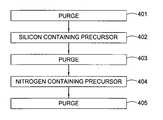
- FIGS. 3 and 4concurrently illustrate how the chamber pressure may be manipulated while introducing and exhausting the precursor, carrier, and purge gases into and out of the chamber.
- the chamber pressureis at P o , the lowest pressure of the chamber during deposition.
- the silicon containing precursor and optional carrier gasare introduced into the chamber and the chamber pressure rises quickly to P 1 .
- the supply of the silicon containing precursor and optional carrier gascontinues at chamber pressure of P 1 until t 2 .
- a gradual decrease in chamber pressure to P ois achieved by controlling the decrease in the precursor gas and optional gas introduced into the chamber and controlling the purge gas introduced into the chamber, and controlling the opening of the exhaust valve.
- the nitrogen containing precursor and optional carrier gasare introduced into the chamber and the chamber pressure rises quickly to P 1 .
- the supply of the nitrogen containing precursor and optional carrier gascontinues at chamber pressure of P 1 until t 4 .
- a gradual decrease in chamber pressure to P ois achieved by controlling the decrease in the precursor gas and optional gas introduced into the chamber and controlling the purge gas introduced into the chamber, and controlling the opening of the exhaust valve.
- the slope of the pressure decrease with respect to timeis substantially constant during the purge steps 403 and 405 .
- the slopes for steps 403 and 405may be similar or different depending on the selection of the precursors, the temperature of the substrate support, or other design conditions.
- the initial high concentration of precursors upon introduction to the processing regionallows a rapid saturation of the substrate surface including the open sites on the substrate surface. If the high concentration of precursor is left in the chamber for too long, more than one layer of the precursor constituent will adhere to the surface of the substrate. For example, if too much silicon containing precursor remains along the surface of the substrate after it is purged from the system, the resulting film will have an unacceptably high silicon concentration.
- the controlled, gradual reduction in processing region pressurehelps maintain an even distribution of chemicals along the substrate surface while forcing the extraneous precursor and carrier gases out of the region while simultaneously purging the system with additional purge gas such as nitrogen or argon.
- the controlled, gradual reduction in the processing region pressurealso prevents the temperature decrease that is common with a rapid decrease in pressure.
- the precursor steps 402 and 404include the introduction of the precursor into the chamber.
- the precursor stepsmay also include introduction of carrier gases, such as nitrogen or argon.
- carrier gasessuch as nitrogen or argon.
- a fixed volume of precursormay be heated in a preheat region, and introduced into the processing region to provide a evenly distributed, saturated layer of the precursor gas along the surface of the substrate.
- the time for the introduction of precursor gases and for purging the gasesmay be selected based on a variety of factors.
- the substrate supportmay be heated to a temperature that requires precursor exposure time tailored to prevent chemical deposition along the chamber surfaces.
- the processing region pressure at the introduction of the gases and at the end of the purgemay influence time selection.
- the precursorsneed various amounts of time to fully chemisorb along the surface of the substrate but not overly coat the surface with an excess of chemicals that could distort the chemical composition of the resulting film.
- the chemical properties of the precursorssuch as their chemical mass, heat of formation, or other properties may influence how much time is needed to move the chemicals through the system or how long the chemical reaction along the surface of the substrate may require.
- the chemical properties of the deposits along the surfaces of the chambermay require additional time to purge the system.
- the time period for the introduction of precursor and optional carrier gasesranges from 1 to 5 seconds and the time period for the purge steps ranges from 2 to 10 seconds.
- HCDS or DCSare the preferred silicon containing precursors.
- the partial pressure HCDSis limited by the byproduct formation and the cost of the precursor.
- the preferred mole fraction of the introduction of the precursor0.05 to 0.3.
- Ammoniais the preferred nitrogen containing precursor which also has a preferred inlet gas mole fraction of 0.05 to 0.3.
- the pressure of the processing regionmay be controlled by manipulating the process hardware such as inlet and exhaust valves under the control of software. Pressure of the system as illustrated by FIG. 3 may range from 0.1 Torr to 30 Torr for this process. Purge pressure in the processing region of a chamber at its lowest point in the deposition process is about 0.2 to 2 Torr while the precursor and carrier gases may be introduced into the deposition chamber at about 2 to about 10 Torr. The temperature of the substrate support may be adjusted to about 400 to 650° C.
- the introduction of gases into the chambermay include preheating the precursors and/or carrier gas, especially when precursors that are unlikely to be gas at room temperature are selected for the process.
- the gasesmay be preheated to about 100 to 250° C. to achieve sufficient vapor pressure and vaporization rate for delivery to a processing region. Heating SiI 4 above about 180° C. may be needed. Preheating the precursor delivery system helps avoid condensation of the precursor in the delivery line, the processing region, and the exhaust assembly of a chamber.
- Five mechanismsmay be employed to reduce ammonium salt formation and contamination of the processing region. Generally, the mechanisms minimize the formation of ammonium salts by removing hydrogen halogen compounds from the processing region or removing the salts after formation by contacting the salts with a gaseous alkene or alkyne species.
- an HY acceptorsuch as acetylene or ethylene can be employed as an additive.
- Including an HY acceptor in deposition precursor mixturesallows the salts to be efficiently removed from the reactor and can facilitate the removal of halogen atoms dissociated from the silicon or nitrogen containing precursors.
- Other HY acceptor additivesinclude alkenes which can be halogenated or unhalogenated, strained ring systems such as norborene and methylene cyclopentene, and silyl hydrides such as SiH 4 .
- Using organic additivesmay also be a benefit to the deposition process because the additives may be selected to tailor carbon addition to the film.
- Controlling the carbon addition to the filmis desirable because tailored carbon content reduces the wet etch rate, improves dry etch selectivity for SiO 2 , lowers the dielectric constant and refractive index, provides improved insulation characteristics, and may also reduce electrical leakage. High corner etch selectivity may also be obtained with tailored carbon addition.
- silyl hydride additivessuch as silane may be employed as HI acceptors. Including HI acceptors reduces the negative effects of ammonium salt in the processing region by trapping out the NH 41 that does form.
- silicon containing precursorsinclude those with formulas SiX n Y 4-n or Si 2 X n Y 6-n .
- a nitrogen source other than ammonia as the nitrogen containing precursormay be employed, thus eliminating a raw material for the formation of the ammonium salts.
- a nitrogen sourceother than ammonia as the nitrogen containing precursor
- less HYis produced than when ammonia is employed.
- Tralkyl aminesare thermodynamically more desirable and produce no HY when used as a nitrogen containing precursor.
- an HY accepting moietysuch as a cyclopropyl group or an allyl group can be incorporated into a nitrogen source such as an amine to make a resulting bifunctional compound such as cyclopropylamine or allylamine.
- a nitrogen sourcesuch as an amine
- This methodreduces the need to add a third component to the precursor gas inlet. It also increases the likelihood that an HI acceptor combines with an HY acceptor. This method also may be especially desirable at temperatures below 500° C.
- FIG. 5illustrates how the wafer to wafer nonuniformity (in percent) and the deposition rate (in ⁇ /cycle) are related to the temperature of deposition from 450 to 550° C. using HCDS and ammonia as the precursors.
- FIG. 6illustrates how pressure from 0.2 to 7 Torr during the introduction of the precursor gases effects the wafer to wafer nonuniformity.
- the filmswere deposited using HCDS and ammonia at 550° C. Fourier transform infrared spectroscopy analysis revealed that the film was Si 3 N 4 .
- the step coverage for the filmexceeded 95 percent.
- the processalso yielded chlorine content of less than 1 percent.
- Deposition ratesincreased to 2 ⁇ /cycle at 590° C. and decreased to 0.8 ⁇ /cycle at 470° C. Boron diffusion through the resulting film is also reduced at lower temperatures.
- Table 1summarizes additional experimental results at 550° C. TABLE 1 Testing results for silicon nitride film deposited at 550° C.
- Ais the silicon precursor (HCDS)
- Bis the nitrogen precursor (ammonia)
- Cis the additive (t-butylamine).
- Rate Refractive WER Recipe ⁇ /cycle Index ⁇ /min A ⁇ B1.9 1.95 13 A ⁇ C 1.0 1.93 1 A ⁇ B ⁇ C 1.65 1.93 3 A ⁇ C ⁇ B 1.85 1.94 4 A ⁇ B ⁇ A ⁇ C 1.70 1.92 4 A ⁇ 33% B + 67% C 1.80 1.93 4 A ⁇ 67% B + 33% C 2.0 1.94 9 A ⁇ 50% B + 50% C 2 H 4 1.9 2.0 7
- Films deposited with the A ⁇ C ⁇ A ⁇ C sequencecontain up to 20 percent carbon while the A ⁇ B ⁇ A ⁇ B sequence film contained no carbon. Other recipes led to intermediate values of carbon in the film. If C 2 H 4 is substituted for t-butylamine in the sequence A ⁇ 50% B+50% C, the wet etch rate of the film is reduced appreciably while the deposition rate and refractive index are almost unaffected. In addition, the carbon content is at detection limits (less than 1 atomic percentage).
- the precursors described hereinmay also be employed in low temperature deposition of silicon oxides.
- the processcan employ O 2 , O 3 , H 2 O, H 2 O 2 , N 2 O, or Ar and O 2 with remote plasma as the oxidant.
- the precursorscan also be employed in the low temperature deposition of oxynitrides wherein N 2 O 2 is employed as both a nitrogen and an oxygen source.
Landscapes
- Chemical & Material Sciences (AREA)
- Engineering & Computer Science (AREA)
- Chemical Kinetics & Catalysis (AREA)
- Materials Engineering (AREA)
- General Chemical & Material Sciences (AREA)
- Organic Chemistry (AREA)
- Metallurgy (AREA)
- Mechanical Engineering (AREA)
- Power Engineering (AREA)
- Condensed Matter Physics & Semiconductors (AREA)
- General Physics & Mathematics (AREA)
- Physics & Mathematics (AREA)
- Manufacturing & Machinery (AREA)
- Microelectronics & Electronic Packaging (AREA)
- Computer Hardware Design (AREA)
- Inorganic Chemistry (AREA)
- Chemical Vapour Deposition (AREA)
- Formation Of Insulating Films (AREA)
Abstract
Description
- 1. Field of the Invention
- Embodiments of the present invention generally relate to substrate processing. More particularly, the invention relates to chemical vapor deposition processes.
- 2. Description of the Related Art
- Chemical vapor deposited (CVD) films are used to form layers of materials within integrated circuits. CVD films are used as insulators, diffusion sources, diffusion and implantation masks, spacers, and final passivation layers. The films are often deposited in chambers that are designed with specific heat and mass transfer properties to optimize the deposition of a physically and chemically uniform film across the surface of a substrate. The chambers are often part of a larger integrated tool to manufacture multiple components on the substrate surface. The chambers are designed to process one substrate at a time or to process multiple substrates.
- As device geometries shrink to enable faster integrated circuits, it is desirable to reduce thermal budgets of deposited films while satisfying increasing demands for high productivity, novel film properties, and low foreign matter. Historically, CVD was performed at temperatures of 700° C. or higher in a batch furnace where deposition occurs in low pressure conditions over a period of a few hours. Lower thermal budget can be achieved by lowering deposition temperature. Low deposition temperature requires the use of low temperature precursors or reducing deposition time.
- Silicon halides have been used as low temperature silicon sources (see, Skordas, et al., Proc. Mat. Res. Soc. Symp. (2000) 606:109-114). In particular, silicon tetraiodide or tetraiodosilane (SiI4) has been used with ammonia (NH3) to deposit silicon nitride at temperatures below 500° C. The silicon nitride deposition rate is roughly independent of precursor exposure once a threshold exposure is exceeded.
FIG. 1 illustrates how the normalized deposition rate as a function of silicon precursor exposure time reaches a maximum asymptotically and thus, the time for precursor exposure may be estimated. The temperature was 450° C. SiI4was the silicon containing precursor with a partial pressure of 0.5 Torr and ammonia was the nitrogen containing precursor. - However, SiI4is a solid with low volatility making low temperature silicon nitride deposition process difficult. Also, these films are nitrogen rich, with a silicon to nitrogen content ratio of about 0.66 compared with a silicon to nitrogen content ratio of about 0.75 for stochiometric films. The films also contain about 16 to 20 percent hydrogen. The high hydrogen content of these materials can be detrimental to device performance by enhancing boron diffusion through the gate dielectric for positive channel metal oxide semiconductor (PMOS) devices and by deviating from stoichiometric film wet etch rates. That is, the wet etch rates using HF or hot phosphoric acid for the low temperature SiI4film is three to five times higher than the wet etch rates for silicon nitride films deposited using dichlorosilane and ammonia at 750° C. Also, using ammonia as a nitrogen containing precursor with silicon halides for the deposition of silicon nitride films results in the formation of ammonium salts such as NH4Cl, NH4BR, NH4I, and others.
- Another method of depositing silicon nitride film at low temperature uses hexachlorodisilane (HCDS) (Si2Cl6) with ammonia (see Tanaka, et al., J. Electrochem. Soc. 147: 2284-2289, U.S. Patent Application Publication 2002/0164890, and U.S. Patent Application Publication 2002/0024119).
FIG. 2 illustrates how the deposition rate does not asymptote to a constant value for large exposure doses, but monotonically increases without reaching a saturation value even with large exposure doses. This is the gradual decomposition of the surface chemisorbed HCDS when it is exposed to additional HCDS in the gas phase to form a S1—Cl2layer on the surface with the possible creation of SiCl4. Introducing SiCl4with HCDS was found to slightly reduce the decomposition of the HCDS in the chamber. The nitrogen containing precursor for this experiment was ammonia. - When HCDS decomposes, the thickness of the deposited film may not occur uniformly across the substrate. Wafer to wafer film thickness variations may also occur. The film stochiometry is degraded. The films are silicon rich and contain substantial amounts of chlorine. These deviations may lead to electrical leakage in the final product. To prevent HCDS decomposition, limiting the partial pressure and exposure time of HCDS has been tested. U.S. Patent Application 20020164890 describes controlling chamber pressure to 2 Torr and using a large flow rate of carrier gas to reduce the HCDS partial pressure. However, to achieve adequate saturation of the surface for deposition rates exceeding 2 Å per cycle, long exposure times such as 30 seconds are necessary. If the exposure time is reduced, the deposition rate can drop below 1.5 Å per cycle.
- Substrate surface saturation with HCDS may also be improved by maintaining convective gas flow across the wafer to distribute reactants evenly. This is described in U.S. Pat. Nos. 5,551,985 and 6,352,593.
- An additional problem with low temperature silicon nitride deposition is the condensation of precursors and the reaction byproducts on the chamber surfaces. As these deposits release from the chamber surfaces and become friable, they may contaminate the substrate. Ammonium salt formation is more likely to occur at low temperature silicon nitride deposition because of the evaporation and sublimation temperatures of the salts. For example, NH4Cl evaporates at 150° C.
- Thus, a need exists for low temperature silicon nitride deposition that discourages the formation of ammonium salts and utilizes effective precursors and efficient process conditions.
- The present invention generally provides a method for depositing a layer comprising silicon and nitrogen on a substrate within a processing region. According to an embodiment of the present invention, the method includes the steps of introducing a silicon containing precursor into the processing region, exhausting gases in the processing region including the silicon containing precursor while uniformly, gradually reducing a pressure of the processing region, introducing a nitrogen containing precursor into the processing region, and exhausting gases in the processing region including the nitrogen containing precursor while uniformly, gradually reducing a pressure of the processing region. According to an aspect of the invention, the slope of the pressure decrease with respect to time during the steps of exhausting is substantially constant.
- So that the manner in which the above recited features of the present invention can be understood in detail, a more particular description of the invention, briefly summarized above, may be had by reference to embodiments, some of which are illustrated in the appended drawings. It is to be noted, however, that the appended drawings illustrate only typical embodiments of this invention and are therefore not to be considered limiting of its scope, for the invention may admit to other equally effective embodiments.
FIG. 1 is a chart of the normalized deposition rate as a function of silicon source exposure time (prior art).FIG. 2 is a chart of the deposition rate as a function of pressure for two temperatures (prior art).FIG. 3 is a chart of pressure as a function of time.FIG. 4 is a flow chart of elements for depositing a silicon nitride film.FIG. 5 is a chart of the deposition rate and WiW non-uniformity as functions of temperature.FIG. 6 is a chart of the wafer non-uniformity as a function of pressure.- The present invention provides methods and apparatus for substrate processing including low temperature deposition of silicon nitride films. This detailed description will describe silicon containing precursors, nitrogen containing precursors, and other process gases. Next, process conditions will be described. Finally, experimental results and advantages will be presented. This invention may be performed in a FlexStar™ chamber available from Applied Materials, Inc. of Santa Clara, Calif. or any other chamber configured for substrate processing under conditions specified herein. Detailed hardware information may be found in U.S. Pat. No. 6,352,593, U.S. Pat. No. 6,352,594, U.S. patent application Ser. No. 10/216,079, and U.S. patent application Ser. No. 10/342,151 which are incorporated by reference herein. Carrier gases for the introduction of the precursor gases include argon and nitrogen. Purge gases for the purge steps in the process include argon and nitrogen.
- Silicon Containing Precursors
- Silicon containing precursors for low temperature silicon nitride deposition are hexachlorodisilane and dichlorosiline. The silicon containing precursor may be selected because it is a liquid or solid at room temperature that easily vaporizes or sublimes at preheat temperatures. Other silicon containing precursors include the silicon halides, such as SiI4, SiBr4, SiH2I2, SiH2Br2, SiCl4, Si2H2Cl2, SiHCl3, Si2Cl6, and more generally, SiXnY4-nor Si2XnY6-n, where X is hydrogen or an organic ligand and Y is a halogen such as Cl, Br, F, or1. Higher order halosilanes are also possible, but typically precursor volatility decreases and thermal stability decreases as the number of silicon atoms in the molecule increases. Organic components can be selected for their size, thermal stability, or other properties and include any straight or branched alkyl group such as methyl, ethyl, propyl, butyl, pentyl, hexyl, heptyl, octyl, nonanyl, decyl, undecyl, dodecyl, substituted alkyl groups, and the isomers thereof such as isopropyl, isobutyl, sec-butyl, tert-butyl, isopentane, isohexane, etc. Aryl groups may also be selected and include pheyl and naphthyl. Allyl groups and substituted allyl groups may be selected. Silicon containing precursors that are desirable for low temperature deposition applications include disilane, silane, trichlorosilane, tetrachlorosilane, and bis(tertiarybutylamino)silane. SiH2I2may also be desirable as a precursor because it is has an very exergonic and exothermic reaction with nitrogen containing precursors compared to other precursors.
- Nitrogen Containing Precursors
- Ammonia is the most common source of nitrogen for low temperature silicon nitride deposition. Alkyl amines such may be selected. Alternatives include dialkylamines and trialkylamines. Specific precursors include trimethylamine, t-butylamine, diallylamine, methylamine, ethylamine, propylamine, butylamine, allylamine, cyclopropylamine, and analogous alkylamines. Hydrazine, hydrazine based derivatives and azides such as alkyl azides, ammonium azide, and others may also be selected. Alternatively, atomic nitrogen can be employed. Atomic nitrogen can be formed from diatomic nitrogen gas in plasma. The plasma can be formed in a reactor separate from the deposition reactor and transported to the deposition reactor via electric or magnetic fields.
- The silicon or nitrogen containing precursor may also be selected based on what type of undesirable deposit is formed along the surfaces of the processing region. Byproduct residue with low melting points is easier to volatilize and exhaust from the chamber than those byproduct residues that have high melting points.
- Process Conditions for Deposition
FIGS. 3 and 4 concurrently illustrate how the chamber pressure may be manipulated while introducing and exhausting the precursor, carrier, and purge gases into and out of the chamber. At time to which is thepurge step 401, the chamber pressure is at Po, the lowest pressure of the chamber during deposition. At time t1which is silicon containingprecursor step 402, the silicon containing precursor and optional carrier gas are introduced into the chamber and the chamber pressure rises quickly to P1. The supply of the silicon containing precursor and optional carrier gas continues at chamber pressure of P1until t2. During thepurge step 403 which occurs from t2to t3, a gradual decrease in chamber pressure to Pois achieved by controlling the decrease in the precursor gas and optional gas introduced into the chamber and controlling the purge gas introduced into the chamber, and controlling the opening of the exhaust valve. At time t3which is nitrogen containingprecursor step 404, the nitrogen containing precursor and optional carrier gas are introduced into the chamber and the chamber pressure rises quickly to P1. The supply of the nitrogen containing precursor and optional carrier gas continues at chamber pressure of P1until t4. During thepurge step 405 which occurs from t4to t5, a gradual decrease in chamber pressure to Pois achieved by controlling the decrease in the precursor gas and optional gas introduced into the chamber and controlling the purge gas introduced into the chamber, and controlling the opening of the exhaust valve. The slope of the pressure decrease with respect to time is substantially constant during the purge steps403 and405. The slopes forsteps - The initial high concentration of precursors upon introduction to the processing region allows a rapid saturation of the substrate surface including the open sites on the substrate surface. If the high concentration of precursor is left in the chamber for too long, more than one layer of the precursor constituent will adhere to the surface of the substrate. For example, if too much silicon containing precursor remains along the surface of the substrate after it is purged from the system, the resulting film will have an unacceptably high silicon concentration. The controlled, gradual reduction in processing region pressure helps maintain an even distribution of chemicals along the substrate surface while forcing the extraneous precursor and carrier gases out of the region while simultaneously purging the system with additional purge gas such as nitrogen or argon. The controlled, gradual reduction in the processing region pressure also prevents the temperature decrease that is common with a rapid decrease in pressure.
- The precursor steps402 and404 include the introduction of the precursor into the chamber. The precursor steps may also include introduction of carrier gases, such as nitrogen or argon. Further, a fixed volume of precursor may be heated in a preheat region, and introduced into the processing region to provide a evenly distributed, saturated layer of the precursor gas along the surface of the substrate.
- The time for the introduction of precursor gases and for purging the gases may be selected based on a variety of factors. The substrate support may be heated to a temperature that requires precursor exposure time tailored to prevent chemical deposition along the chamber surfaces. The processing region pressure at the introduction of the gases and at the end of the purge may influence time selection. The precursors need various amounts of time to fully chemisorb along the surface of the substrate but not overly coat the surface with an excess of chemicals that could distort the chemical composition of the resulting film. The chemical properties of the precursors, such as their chemical mass, heat of formation, or other properties may influence how much time is needed to move the chemicals through the system or how long the chemical reaction along the surface of the substrate may require. The chemical properties of the deposits along the surfaces of the chamber may require additional time to purge the system. In the illustrated embodiment, the time period for the introduction of precursor and optional carrier gases ranges from 1 to 5 seconds and the time period for the purge steps ranges from 2 to 10 seconds.
- HCDS or DCS are the preferred silicon containing precursors. The partial pressure HCDS is limited by the byproduct formation and the cost of the precursor. The preferred mole fraction of the introduction of the precursor 0.05 to 0.3. Ammonia is the preferred nitrogen containing precursor which also has a preferred inlet gas mole fraction of 0.05 to 0.3.
- The pressure of the processing region may be controlled by manipulating the process hardware such as inlet and exhaust valves under the control of software. Pressure of the system as illustrated by
FIG. 3 may range from 0.1 Torr to 30 Torr for this process. Purge pressure in the processing region of a chamber at its lowest point in the deposition process is about 0.2 to 2 Torr while the precursor and carrier gases may be introduced into the deposition chamber at about 2 to about 10 Torr. The temperature of the substrate support may be adjusted to about 400 to 650° C. - The introduction of gases into the chamber may include preheating the precursors and/or carrier gas, especially when precursors that are unlikely to be gas at room temperature are selected for the process. The gases may be preheated to about 100 to 250° C. to achieve sufficient vapor pressure and vaporization rate for delivery to a processing region. Heating SiI4above about 180° C. may be needed. Preheating the precursor delivery system helps avoid condensation of the precursor in the delivery line, the processing region, and the exhaust assembly of a chamber.
- Process for Reducing Ammonium Salt Formation
- Five mechanisms may be employed to reduce ammonium salt formation and contamination of the processing region. Generally, the mechanisms minimize the formation of ammonium salts by removing hydrogen halogen compounds from the processing region or removing the salts after formation by contacting the salts with a gaseous alkene or alkyne species.
- First, an HY acceptor such as acetylene or ethylene can be employed as an additive. Including an HY acceptor in deposition precursor mixtures allows the salts to be efficiently removed from the reactor and can facilitate the removal of halogen atoms dissociated from the silicon or nitrogen containing precursors. Other HY acceptor additives include alkenes which can be halogenated or unhalogenated, strained ring systems such as norborene and methylene cyclopentene, and silyl hydrides such as SiH4. Using organic additives may also be a benefit to the deposition process because the additives may be selected to tailor carbon addition to the film. Controlling the carbon addition to the film is desirable because tailored carbon content reduces the wet etch rate, improves dry etch selectivity for SiO2, lowers the dielectric constant and refractive index, provides improved insulation characteristics, and may also reduce electrical leakage. High corner etch selectivity may also be obtained with tailored carbon addition.
- Second, silyl hydride additives such as silane may be employed as HI acceptors. Including HI acceptors reduces the negative effects of ammonium salt in the processing region by trapping out the NH41that does form.
- Third, compounds that act as both silicon containing precursors and HI acceptors may be employed to both provide silicon to the process and to effectively remove the salts from the chamber. Acceptable silicon containing precursors include those with formulas SiXnY4-nor Si2XnY6-n.
- Fourth, a nitrogen source other than ammonia as the nitrogen containing precursor may be employed, thus eliminating a raw material for the formation of the ammonium salts. For example, when an alkyl amine is employed as a nitrogen source, less HY is produced than when ammonia is employed. Tralkyl amines are thermodynamically more desirable and produce no HY when used as a nitrogen containing precursor.
- Finally, an HY accepting moiety such as a cyclopropyl group or an allyl group can be incorporated into a nitrogen source such as an amine to make a resulting bifunctional compound such as cyclopropylamine or allylamine. This method reduces the need to add a third component to the precursor gas inlet. It also increases the likelihood that an HI acceptor combines with an HY acceptor. This method also may be especially desirable at temperatures below 500° C.
- These five methods may be individually employed or combined in any fashion to help reduce ammonium salt formation.
- Experimental Results
- Modifying the traditional purge system to have a gradual and uniform reduction in processing region pressure as described in
FIGS. 3 and 4 results in a higher level of precursor surface saturation without partial decomposition of the precursor.FIG. 5 illustrates how the wafer to wafer nonuniformity (in percent) and the deposition rate (in Å/cycle) are related to the temperature of deposition from 450 to 550° C. using HCDS and ammonia as the precursors.FIG. 6 illustrates how pressure from 0.2 to 7 Torr during the introduction of the precursor gases effects the wafer to wafer nonuniformity. The films were deposited using HCDS and ammonia at 550° C. Fourier transform infrared spectroscopy analysis revealed that the film was Si3N4. The step coverage for the film exceeded 95 percent. The process also yielded chlorine content of less than 1 percent. Deposition rates increased to 2 Å/cycle at 590° C. and decreased to 0.8 Å/cycle at 470° C. Boron diffusion through the resulting film is also reduced at lower temperatures. Table 1 below summarizes additional experimental results at 550° C.TABLE 1 Testing results for silicon nitride film deposited at 550° C. Parameter Value Comment Deposition rate 1.5-1.6 A/cycle Below saturation value WiWNU <±1.5% R/2M Refractive index 1.99 >300 Å film Stoichiometry Si:N˜0.74 Stoichiometric Impurities H˜8% Cl˜0.9% Atomic % Surface roughness Ra˜3.7 Å ˜417 Å film Wet etch rates 31.5 Å/min 100:1 HF, 2 min. 222 Å/min Hot H3PO4, 0.5 min. Shrinkage ˜4.3% 850° C., 60 min N2anneal Stress 450 MPa tensile 1620 MPa after anneal Step coverage ˜100% 40:1 AR deep trench Microloading 0-5% Limited by SEM resolution Metal contamination TXRF detection limits Including Ti In-film Particles <50 (>0.2 μm) 100 Å film, SP-1 - Introducing a carrier gas or an additive such as hydrogen or disilane also modifies the resulting film properties. Table 2 illustrates the observed deposition rates, refractive index, silicon to nitrogen ratio, and hydrogen percentage observed in films created by using different split recipes. By utilizing a carrier gas that does not comprise nitrogen or a carrier gas and comprises an additive, the hydrogen content and silicon to nitrogen ratio of the film can be improved.
TABLE 2 Properties of films deposited under baseline conditions and with additives. Rate [H] Split Å/min R.I. Si:N At. % Baseline (w/N2) 14.5 1.800 0.65 20.2 Baseline (w/Ar) 13.5 1.799 0.72 20.5 Low pressure (0.5 Torr) 6.76 1.811 0.65 19.1 NH3:Si source˜20:1 17.9 1.807 0.65 19.7 NH3:Si source˜4:1 12.0 1.795 0.72 20.1 Hydrogen Additive 14.3 1.804 0.65 19.4 Disilane Additive 20.6 2.386 1.0 11.3 - There are a variety of ways to control the addition of carbon. In Table 3, A is the silicon precursor (HCDS), B is the nitrogen precursor (ammonia), and C is the additive (t-butylamine).
TABLE 3 Deposition rates, refractive index, and wet etch rate for varied deposition processes. Rate Refractive WER Recipe Å/cycle Index Å/min A → B 1.9 1.95 13 A → C 1.0 1.93 1 A → B → C 1.65 1.93 3 A → C → B 1.85 1.94 4 A → B → A → C 1.70 1.92 4 A → 33% B + 67% C 1.80 1.93 4 A → 67% B + 33% C 2.0 1.94 9 A → 50% B + 50% C2H4 1.9 2.0 7 - Films deposited with the A→C→A→C sequence contain up to 20 percent carbon while the A→B→A→B sequence film contained no carbon. Other recipes led to intermediate values of carbon in the film. If C2H4is substituted for t-butylamine in the sequence A→50% B+50% C, the wet etch rate of the film is reduced appreciably while the deposition rate and refractive index are almost unaffected. In addition, the carbon content is at detection limits (less than 1 atomic percentage).
- Introducing carbon in controlled amounts improves wet etch rates in 100:1 HF by a factor of 1.5 to 10. The reduction in dry etch rates with the addition of carbon were by a factor of 1.25 to 1.5. This improved wet etch rate was observed by using ethylene, t-butylamine and diallylamine as HY acceptors in conjunction with Si2CL6and ammonia.
- Introducing SiCl4with HCDS was found to reduce the likelihood of decomposition of HCDS to form SiCl2.
- The precursors described herein may also be employed in low temperature deposition of silicon oxides. The process can employ O2, O3, H2O, H2O2, N2O, or Ar and O2with remote plasma as the oxidant. The precursors can also be employed in the low temperature deposition of oxynitrides wherein N2O2is employed as both a nitrogen and an oxygen source.
- While the foregoing is directed to embodiments of the present invention, other and further embodiments of the invention may be devised without departing from the basic scope thereof, and the scope thereof is determined by the claims that follow.
Claims (20)
1. A method for depositing a layer comprising silicon and nitrogen on a substrate within a processing region, comprising:
introducing a silicon containing precursor into the processing region;
exhausting gases in the processing region including the silicon containing precursor while uniformly, gradually reducing a pressure of the processing region;
introducing a nitrogen containing precursor into the processing region; and
exhausting gases in the processing region including the nitrogen containing precursor while uniformly, gradually reducing a pressure of the processing region.
2. The method ofclaim 1 , further comprising maintaining a support for the substrate at a temperature of 400 to 650° C.
3. The method ofclaim 1 , wherein the pressure of the processing region is 0.2 to 10 Torr.
4. The method ofclaim 1 , wherein a slope of pressure decrease with respect to time during each step of exhausting is substantially constant.
5. The method ofclaim 4 , wherein the slopes of the pressure decrease with respect to time during the steps of exhausting are substantially the same.
6. The method ofclaim 4 , wherein a time period for introducing the silicon containing precursor and a time period for introducing the nitrogen containing precursor is 1 to 5 seconds.
7. The method ofclaim 4 , wherein a time period for exhausting gases in the processing region including the silicon containing precursor and the nitrogen containing precursor is 2 to 20 seconds.
8. The method ofclaim 1 , wherein a pressure in the processing region while introducing the silicon containing precursor is 0.2 to 10 Torr and a pressure in the processing region while introducing the nitrogen containing precursor is 0.2 to 10 Torr.
9. The method ofclaim 1 , wherein a pressure in the processing region before introducing the silicon containing precursor is 0.2 Torr and a pressure in the processing region before introducing the nitrogen containing precursor is 0.2 Torr.
10. The method ofclaim 1 , wherein the nitrogen containing precursor is selected from the group comprising ammonia, trimethylamine, t-butylamine, diallylamine, methylamine, ethylamine, propylamine, butylamine, allylamine, and cyclopropylamine.
11. The method ofclaim 1 , wherein the silicon containing precursor is selected from the group comprising disilane, silane, trichlorosilane, tetrachlorosilane, and bis(tertiarybutylamino)silane.
12. A method for depositing a layer comprising silicon and nitrogen on a substrate within a processing region, comprising:
preheating a silicon containing precursor and a nitrogen containing precursor;
introducing a silicon containing precursor into the processing region;
exhausting gases in the processing region including the silicon containing precursor while uniformly, gradually reducing a pressure of the processing region;
introducing a nitrogen containing precursor into the processing region; and
exhausting gases in the processing region including the nitrogen containing precursor while uniformly, gradually reducing a pressure of the processing region.
13. The method ofclaim 12 , wherein the silicon containing precursor and the nitrogen containing precursor are preheated to 100 to 250° C.
14. The method ofclaim 12 , wherein the pressure of the processing region is reduced during the steps of exhausting by controlling an amount of purge gas introduced into the processing region and by controlling an exhaust valve in communication with the processing region.
15. The method ofclaim 12 , wherein the nitrogen containing precursor is selected from the group comprising ammonia, trimethylamine, t-butylamine, diallylamine, methylamine, ethylamine, propylamine, butylamine, allylamine, and cyclopropylamine and the silicon containing precursor is selected from the group comprising disilane, silane, trichlorosilane, tetrachlorosilane, and bis(tertiarybutylamino)silane.
16. The method ofclaim 12 , wherein a support for the substrate in the processing region is maintained at a temperature of 400 to 650° C.
17. The method ofclaim 12 , wherein a pressure of the processing region is 0.2 to 10 Torr.
18. A method for depositing a layer comprising silicon and nitrogen on a substrate in a processing region, comprising:
introducing a silicon containing precursor into the processing region;
exhausting gases in the processing region including the silicon containing precursor while reducing a pressure of the processing region such that a slope of pressure decrease with respect to time is substantially constant;
introducing a nitrogen containing precursor into the processing region; and
exhausting gases in the processing region including the nitrogen containing precursor while reducing a pressure of the processing region such that a slope of pressure decrease with respect to time is substantially constant.
19. The method ofclaim 18 , wherein a time period for introducing the silicon and nitrogen containing precursors is 1-5 seconds and a time period for exhausting gases including the silicon and nitrogen containing precursors is 2-20 seconds.
20. The method ofclaim 18 , wherein a pressure of the processing region is 0.2 to 10 Torr.
Priority Applications (6)
| Application Number | Priority Date | Filing Date | Title |
|---|---|---|---|
| US10/970,317US20060084283A1 (en) | 2004-10-20 | 2004-10-20 | Low temperature sin deposition methods |
| PCT/US2005/029037WO2006044019A2 (en) | 2004-10-20 | 2005-08-15 | Low temperature sin deposition methods |
| KR1020077010723AKR20070061593A (en) | 2004-10-20 | 2005-08-15 | Low Temperature SIN Deposition Method |
| EP05806517AEP1825019A2 (en) | 2004-10-20 | 2005-08-15 | Low temperature sin deposition methods |
| JP2007537880AJP2008517479A (en) | 2004-10-20 | 2005-08-15 | SiN low temperature deposition method |
| CNA2005800393940ACN101061255A (en) | 2004-10-20 | 2005-08-15 | Low temperature SiN deposition methods |
Applications Claiming Priority (1)
| Application Number | Priority Date | Filing Date | Title |
|---|---|---|---|
| US10/970,317US20060084283A1 (en) | 2004-10-20 | 2004-10-20 | Low temperature sin deposition methods |
Publications (1)
| Publication Number | Publication Date |
|---|---|
| US20060084283A1true US20060084283A1 (en) | 2006-04-20 |
Family
ID=36088362
Family Applications (1)
| Application Number | Title | Priority Date | Filing Date |
|---|---|---|---|
| US10/970,317AbandonedUS20060084283A1 (en) | 2004-10-20 | 2004-10-20 | Low temperature sin deposition methods |
Country Status (6)
| Country | Link |
|---|---|
| US (1) | US20060084283A1 (en) |
| EP (1) | EP1825019A2 (en) |
| JP (1) | JP2008517479A (en) |
| KR (1) | KR20070061593A (en) |
| CN (1) | CN101061255A (en) |
| WO (1) | WO2006044019A2 (en) |
Cited By (87)
| Publication number | Priority date | Publication date | Assignee | Title |
|---|---|---|---|---|
| US20050118837A1 (en)* | 2002-07-19 | 2005-06-02 | Todd Michael A. | Method to form ultra high quality silicon-containing compound layers |
| US20060060137A1 (en)* | 2004-09-22 | 2006-03-23 | Albert Hasper | Deposition of TiN films in a batch reactor |
| US20060088985A1 (en)* | 2002-07-19 | 2006-04-27 | Ruben Haverkort | Low temperature silicon compound deposition |
| US20060199357A1 (en)* | 2005-03-07 | 2006-09-07 | Wan Yuet M | High stress nitride film and method for formation thereof |
| US20060286818A1 (en)* | 2005-06-17 | 2006-12-21 | Yaxin Wang | Method for silicon based dielectric chemical vapor deposition |
| US20070141812A1 (en)* | 2005-12-16 | 2007-06-21 | Zagwijn Peter M | Low temperature doped silicon layer formation |
| US20070224830A1 (en)* | 2005-01-31 | 2007-09-27 | Samoilov Arkadii V | Low temperature etchant for treatment of silicon-containing surfaces |
| US20080014761A1 (en)* | 2006-06-29 | 2008-01-17 | Ritwik Bhatia | Decreasing the etch rate of silicon nitride by carbon addition |
| US20080145536A1 (en)* | 2006-12-13 | 2008-06-19 | Applied Materials, Inc. | METHOD AND APPARATUS FOR LOW TEMPERATURE AND LOW K SiBN DEPOSITION |
| US20080274605A1 (en)* | 2004-07-29 | 2008-11-06 | Semiconductor Leading Edge Technologies, Inc. | Method of manufacturing silicon nitride film, method of manufacturing semiconductor device, and semiconductor device |
| US7659158B2 (en) | 2008-03-31 | 2010-02-09 | Applied Materials, Inc. | Atomic layer deposition processes for non-volatile memory devices |
| US7691757B2 (en) | 2006-06-22 | 2010-04-06 | Asm International N.V. | Deposition of complex nitride films |
| US7794544B2 (en) | 2004-05-12 | 2010-09-14 | Applied Materials, Inc. | Control of gas flow and delivery to suppress the formation of particles in an MOCVD/ALD system |
| US7798096B2 (en) | 2006-05-05 | 2010-09-21 | Applied Materials, Inc. | Plasma, UV and ion/neutral assisted ALD or CVD in a batch tool |
| US7833906B2 (en) | 2008-12-11 | 2010-11-16 | Asm International N.V. | Titanium silicon nitride deposition |
| US20110256734A1 (en)* | 2010-04-15 | 2011-10-20 | Hausmann Dennis M | Silicon nitride films and methods |
| JP2013153164A (en)* | 2012-01-20 | 2013-08-08 | Novellus Systems Incorporated | METHOD FOR DEPOSITING A CHLORINE-FREE CONFORMAL SiN FILM |
| US8637411B2 (en) | 2010-04-15 | 2014-01-28 | Novellus Systems, Inc. | Plasma activated conformal dielectric film deposition |
| US8647993B2 (en) | 2011-04-11 | 2014-02-11 | Novellus Systems, Inc. | Methods for UV-assisted conformal film deposition |
| US20140273531A1 (en)* | 2013-03-14 | 2014-09-18 | Asm Ip Holding B.V. | Si PRECURSORS FOR DEPOSITION OF SiN AT LOW TEMPERATURES |
| US20140273477A1 (en)* | 2013-03-14 | 2014-09-18 | Asm Ip Holding B.V. | Si PRECURSORS FOR DEPOSITION OF SiN AT LOW TEMPERATURES |
| US20140273528A1 (en)* | 2013-03-14 | 2014-09-18 | Asm Ip Holding B.V. | Si PRECURSORS FOR DEPOSITION OF SiN AT LOW TEMPERATURES |
| US8956983B2 (en) | 2010-04-15 | 2015-02-17 | Novellus Systems, Inc. | Conformal doping via plasma activated atomic layer deposition and conformal film deposition |
| US9076646B2 (en) | 2010-04-15 | 2015-07-07 | Lam Research Corporation | Plasma enhanced atomic layer deposition with pulsed plasma exposure |
| US9214334B2 (en) | 2014-02-18 | 2015-12-15 | Lam Research Corporation | High growth rate process for conformal aluminum nitride |
| US9214333B1 (en) | 2014-09-24 | 2015-12-15 | Lam Research Corporation | Methods and apparatuses for uniform reduction of the in-feature wet etch rate of a silicon nitride film formed by ALD |
| US9257274B2 (en) | 2010-04-15 | 2016-02-09 | Lam Research Corporation | Gapfill of variable aspect ratio features with a composite PEALD and PECVD method |
| US9287113B2 (en) | 2012-11-08 | 2016-03-15 | Novellus Systems, Inc. | Methods for depositing films on sensitive substrates |
| US9355886B2 (en) | 2010-04-15 | 2016-05-31 | Novellus Systems, Inc. | Conformal film deposition for gapfill |
| US9355839B2 (en) | 2012-10-23 | 2016-05-31 | Lam Research Corporation | Sub-saturated atomic layer deposition and conformal film deposition |
| US9362109B2 (en) | 2013-10-16 | 2016-06-07 | Asm Ip Holding B.V. | Deposition of boron and carbon containing materials |
| US9373500B2 (en) | 2014-02-21 | 2016-06-21 | Lam Research Corporation | Plasma assisted atomic layer deposition titanium oxide for conformal encapsulation and gapfill applications |
| US9390909B2 (en) | 2013-11-07 | 2016-07-12 | Novellus Systems, Inc. | Soft landing nanolaminates for advanced patterning |
| US9401273B2 (en) | 2013-12-11 | 2016-07-26 | Asm Ip Holding B.V. | Atomic layer deposition of silicon carbon nitride based materials |
| US9478411B2 (en) | 2014-08-20 | 2016-10-25 | Lam Research Corporation | Method to tune TiOx stoichiometry using atomic layer deposited Ti film to minimize contact resistance for TiOx/Ti based MIS contact scheme for CMOS |
| US9478438B2 (en) | 2014-08-20 | 2016-10-25 | Lam Research Corporation | Method and apparatus to deposit pure titanium thin film at low temperature using titanium tetraiodide precursor |
| US9502238B2 (en) | 2015-04-03 | 2016-11-22 | Lam Research Corporation | Deposition of conformal films by atomic layer deposition and atomic layer etch |
| US9564312B2 (en) | 2014-11-24 | 2017-02-07 | Lam Research Corporation | Selective inhibition in atomic layer deposition of silicon-containing films |
| US9576792B2 (en) | 2014-09-17 | 2017-02-21 | Asm Ip Holding B.V. | Deposition of SiN |
| US9576790B2 (en) | 2013-10-16 | 2017-02-21 | Asm Ip Holding B.V. | Deposition of boron and carbon containing materials |
| US9589790B2 (en) | 2014-11-24 | 2017-03-07 | Lam Research Corporation | Method of depositing ammonia free and chlorine free conformal silicon nitride film |
| US9601693B1 (en) | 2015-09-24 | 2017-03-21 | Lam Research Corporation | Method for encapsulating a chalcogenide material |
| US9611544B2 (en) | 2010-04-15 | 2017-04-04 | Novellus Systems, Inc. | Plasma activated conformal dielectric film deposition |
| US9685320B2 (en) | 2010-09-23 | 2017-06-20 | Lam Research Corporation | Methods for depositing silicon oxide |
| US9691972B1 (en) | 2015-12-21 | 2017-06-27 | International Business Machines Corporation | Low temperature encapsulation for magnetic tunnel junction |
| US9773643B1 (en) | 2016-06-30 | 2017-09-26 | Lam Research Corporation | Apparatus and method for deposition and etch in gap fill |
| WO2017201456A1 (en)* | 2016-05-19 | 2017-11-23 | L'air Liquide, Societe Anonyme Pour L'etude Et L'exploitation Des Procedes Georges Claude | Preparation of si-h containing iodosilanes via halide exchange reaction |
| US9837261B2 (en) | 2011-12-09 | 2017-12-05 | Hitachi Kokusai Electric Inc. | Method of manufacturing semiconductor device and substrate processing method |
| US9865455B1 (en) | 2016-09-07 | 2018-01-09 | Lam Research Corporation | Nitride film formed by plasma-enhanced and thermal atomic layer deposition process |
| US9892917B2 (en) | 2010-04-15 | 2018-02-13 | Lam Research Corporation | Plasma assisted atomic layer deposition of multi-layer films for patterning applications |
| US9991112B2 (en)* | 2016-09-28 | 2018-06-05 | Samsung Electronics Co., Ltd. | Method for forming dielectric film and method for fabricating semiconductor device |
| US9997357B2 (en) | 2010-04-15 | 2018-06-12 | Lam Research Corporation | Capped ALD films for doping fin-shaped channel regions of 3-D IC transistors |
| WO2018132568A1 (en)* | 2017-01-13 | 2018-07-19 | Applied Materials, Inc. | Methods and apparatus for low temperature silicon nitride films |
| US10037884B2 (en) | 2016-08-31 | 2018-07-31 | Lam Research Corporation | Selective atomic layer deposition for gapfill using sacrificial underlayer |
| US10062563B2 (en) | 2016-07-01 | 2018-08-28 | Lam Research Corporation | Selective atomic layer deposition with post-dose treatment |
| US10074543B2 (en) | 2016-08-31 | 2018-09-11 | Lam Research Corporation | High dry etch rate materials for semiconductor patterning applications |
| US10134579B2 (en) | 2016-11-14 | 2018-11-20 | Lam Research Corporation | Method for high modulus ALD SiO2 spacer |
| US10269559B2 (en) | 2017-09-13 | 2019-04-23 | Lam Research Corporation | Dielectric gapfill of high aspect ratio features utilizing a sacrificial etch cap layer |
| US10410857B2 (en) | 2015-08-24 | 2019-09-10 | Asm Ip Holding B.V. | Formation of SiN thin films |
| US10454029B2 (en) | 2016-11-11 | 2019-10-22 | Lam Research Corporation | Method for reducing the wet etch rate of a sin film without damaging the underlying substrate |
| US10526701B2 (en) | 2015-07-09 | 2020-01-07 | Lam Research Corporation | Multi-cycle ALD process for film uniformity and thickness profile modulation |
| US10566251B2 (en) | 2018-07-17 | 2020-02-18 | International Business Machines Corporation | Techniques for forming vertical transport FET |
| US10580645B2 (en) | 2018-04-30 | 2020-03-03 | Asm Ip Holding B.V. | Plasma enhanced atomic layer deposition (PEALD) of SiN using silicon-hydrohalide precursors |
| US10629435B2 (en) | 2016-07-29 | 2020-04-21 | Lam Research Corporation | Doped ALD films for semiconductor patterning applications |
| US10832908B2 (en) | 2016-11-11 | 2020-11-10 | Lam Research Corporation | Self-aligned multi-patterning process flow with ALD gapfill spacer mask |
| US20200407228A1 (en)* | 2016-05-19 | 2020-12-31 | L'Air Liquide, Société Anonyme pour l'Etude et l'Exploitation des Procédés Georges Claude | Preparation of si-h containing iodosilanes via halide exchange reaction |
| US11009339B2 (en) | 2018-08-23 | 2021-05-18 | Applied Materials, Inc. | Measurement of thickness of thermal barrier coatings using 3D imaging and surface subtraction methods for objects with complex geometries |
| US11015252B2 (en) | 2018-04-27 | 2021-05-25 | Applied Materials, Inc. | Protection of components from corrosion |
| US11028480B2 (en) | 2018-03-19 | 2021-06-08 | Applied Materials, Inc. | Methods of protecting metallic components against corrosion using chromium-containing thin films |
| US11056353B2 (en) | 2017-06-01 | 2021-07-06 | Asm Ip Holding B.V. | Method and structure for wet etch utilizing etch protection layer comprising boron and carbon |
| US11404275B2 (en) | 2018-03-02 | 2022-08-02 | Lam Research Corporation | Selective deposition using hydrolysis |
| US11466364B2 (en) | 2019-09-06 | 2022-10-11 | Applied Materials, Inc. | Methods for forming protective coatings containing crystallized aluminum oxide |
| US11519066B2 (en) | 2020-05-21 | 2022-12-06 | Applied Materials, Inc. | Nitride protective coatings on aerospace components and methods for making the same |
| US20230034561A1 (en)* | 2020-01-10 | 2023-02-02 | Lam Research Corporation | Ammonia abatement for improved roughing pump performance |
| US11646198B2 (en) | 2015-03-20 | 2023-05-09 | Lam Research Corporation | Ultrathin atomic layer deposition film accuracy thickness control |
| US11694912B2 (en) | 2017-08-18 | 2023-07-04 | Applied Materials, Inc. | High pressure and high temperature anneal chamber |
| US11697879B2 (en) | 2019-06-14 | 2023-07-11 | Applied Materials, Inc. | Methods for depositing sacrificial coatings on aerospace components |
| US11705312B2 (en) | 2020-12-26 | 2023-07-18 | Applied Materials, Inc. | Vertically adjustable plasma source |
| US11732353B2 (en) | 2019-04-26 | 2023-08-22 | Applied Materials, Inc. | Methods of protecting aerospace components against corrosion and oxidation |
| US11739429B2 (en) | 2020-07-03 | 2023-08-29 | Applied Materials, Inc. | Methods for refurbishing aerospace components |
| US11794382B2 (en) | 2019-05-16 | 2023-10-24 | Applied Materials, Inc. | Methods for depositing anti-coking protective coatings on aerospace components |
| US11996286B2 (en) | 2020-12-09 | 2024-05-28 | Asm Ip Holding B.V. | Silicon precursors for silicon nitride deposition |
| US12040181B2 (en) | 2019-05-01 | 2024-07-16 | Lam Research Corporation | Modulated atomic layer deposition |
| US12157945B2 (en) | 2019-08-06 | 2024-12-03 | Lam Research Corporation | Thermal atomic layer deposition of silicon-containing films |
| US12237175B2 (en) | 2019-06-04 | 2025-02-25 | Lam Research Corporation | Polymerization protective liner for reactive ion etch in patterning |
| US12412742B2 (en) | 2020-07-28 | 2025-09-09 | Lam Research Corporation | Impurity reduction in silicon-containing films |
| US12431349B2 (en) | 2019-06-07 | 2025-09-30 | Lam Research Corporation | In-situ control of film properties during atomic layer deposition |
Families Citing this family (10)
| Publication number | Priority date | Publication date | Assignee | Title |
|---|---|---|---|---|
| US7943531B2 (en)* | 2007-10-22 | 2011-05-17 | Applied Materials, Inc. | Methods for forming a silicon oxide layer over a substrate |
| JP2012015344A (en)* | 2010-07-01 | 2012-01-19 | Hitachi Kokusai Electric Inc | Method of manufacturing semiconductor device |
| JP6239079B2 (en)* | 2011-12-09 | 2017-11-29 | 株式会社日立国際電気 | Semiconductor device manufacturing method, substrate processing method, substrate processing apparatus, and program |
| JP6049395B2 (en)* | 2011-12-09 | 2016-12-21 | 株式会社日立国際電気 | Semiconductor device manufacturing method, substrate processing method, substrate processing apparatus, and program |
| CN103928647B (en)* | 2013-01-16 | 2016-02-17 | 海洋王照明科技股份有限公司 | Silicon nitride composite diaphragm and preparation method thereof |
| US10106425B2 (en) | 2016-05-19 | 2018-10-23 | L'Air Liquide, Société Anonyme pour l'Etude et l'Exploitation des Procédés Georges Claude | Synthesis methods for halosilanes |
| US10640523B2 (en)* | 2018-01-12 | 2020-05-05 | Entegris, Inc. | Aminoiodosilanes and methods of synthesizing these aminoiodosilanes |
| JP6789257B2 (en)* | 2018-02-28 | 2020-11-25 | 株式会社Kokusai Electric | Semiconductor device manufacturing methods, substrate processing devices, and programs |
| US10483407B2 (en)* | 2018-04-19 | 2019-11-19 | Micron Technology, Inc. | Methods of forming si3nX, methods of forming insulator material between a control gate and charge-storage material of a programmable charge-storage transistor, and methods of forming an array of elevationally-extending strings of memory cells and a programmable charge-storage transistor manufactured in accordance with methods |
| US11538677B2 (en) | 2020-09-01 | 2022-12-27 | Applied Materials, Inc. | Systems and methods for depositing high density and high tensile stress films |
Citations (75)
| Publication number | Priority date | Publication date | Assignee | Title |
|---|---|---|---|---|
| US5221556A (en)* | 1987-06-24 | 1993-06-22 | Epsilon Technology, Inc. | Gas injectors for reaction chambers in CVD systems |
| US5298287A (en)* | 1993-02-05 | 1994-03-29 | United Technologies Corporation | Method of making CVD Si3 N4 |
| US5300322A (en)* | 1992-03-10 | 1994-04-05 | Martin Marietta Energy Systems, Inc. | Molybdenum enhanced low-temperature deposition of crystalline silicon nitride |
| US5503875A (en)* | 1993-03-18 | 1996-04-02 | Tokyo Electron Limited | Film forming method wherein a partial pressure of a reaction byproduct in a processing container is reduced temporarily |
| US5551985A (en)* | 1995-08-18 | 1996-09-03 | Torrex Equipment Corporation | Method and apparatus for cold wall chemical vapor deposition |
| US5772773A (en)* | 1996-05-20 | 1998-06-30 | Applied Materials, Inc. | Co-axial motorized wafer lift |
| US5910342A (en)* | 1983-08-16 | 1999-06-08 | Canon Kabushiki Kaisha | Process for forming deposition film |
| US5916365A (en)* | 1996-08-16 | 1999-06-29 | Sherman; Arthur | Sequential chemical vapor deposition |
| US6079356A (en)* | 1997-12-02 | 2000-06-27 | Applied Materials, Inc. | Reactor optimized for chemical vapor deposition of titanium |
| US6090442A (en)* | 1997-04-14 | 2000-07-18 | University Technology Corporation | Method of growing films on substrates at room temperatures using catalyzed binary reaction sequence chemistry |
| US6093252A (en)* | 1995-08-03 | 2000-07-25 | Asm America, Inc. | Process chamber with inner support |
| US6103014A (en)* | 1993-04-05 | 2000-08-15 | Applied Materials, Inc. | Chemical vapor deposition chamber |
| US6153261A (en)* | 1999-05-28 | 2000-11-28 | Applied Materials, Inc. | Dielectric film deposition employing a bistertiarybutylaminesilane precursor |
| US6200893B1 (en)* | 1999-03-11 | 2001-03-13 | Genus, Inc | Radical-assisted sequential CVD |
| US6207487B1 (en)* | 1998-10-13 | 2001-03-27 | Samsung Electronics Co., Ltd. | Method for forming dielectric film of capacitor having different thicknesses partly |
| US20010000866A1 (en)* | 1999-03-11 | 2001-05-10 | Ofer Sneh | Apparatus and concept for minimizing parasitic chemical vapor deposition during atomic layer deposition |
| US6270572B1 (en)* | 1998-08-07 | 2001-08-07 | Samsung Electronics Co., Ltd. | Method for manufacturing thin film using atomic layer deposition |
| US6271054B1 (en)* | 2000-06-02 | 2001-08-07 | International Business Machines Corporation | Method for reducing dark current effects in a charge couple device |
| US6284646B1 (en)* | 1997-08-19 | 2001-09-04 | Samsung Electronics Co., Ltd | Methods of forming smooth conductive layers for integrated circuit devices |
| US6287965B1 (en)* | 1997-07-28 | 2001-09-11 | Samsung Electronics Co, Ltd. | Method of forming metal layer using atomic layer deposition and semiconductor device having the metal layer as barrier metal layer or upper or lower electrode of capacitor |
| US20010024871A1 (en)* | 1998-04-24 | 2001-09-27 | Fuji Xerox Co. | Semiconductor device and method and apparatus for manufacturing semiconductor device |
| US20010028924A1 (en)* | 1996-08-16 | 2001-10-11 | Arthur Sherman | Sequential chemical vapor deposition |
| US20010034123A1 (en)* | 2000-04-20 | 2001-10-25 | In-Sang Jeon | Method of manufacturing a barrier metal layer using atomic layer deposition |
| US20010041250A1 (en)* | 2000-03-07 | 2001-11-15 | Werkhoven Christian J. | Graded thin films |
| US20020000598A1 (en)* | 1999-12-08 | 2002-01-03 | Sang-Bom Kang | Semiconductor devices having metal layers as barrier layers on upper or lower electrodes of capacitors |
| US20020016084A1 (en)* | 2000-04-28 | 2002-02-07 | Todd Michael A. | CVD syntheses of silicon nitride materials |
| US20020024119A1 (en)* | 1999-01-08 | 2002-02-28 | Kabushiki Kaisha Toshiba | Semiconductor device and method of manufacturing the same |
| US6352594B2 (en)* | 1997-08-11 | 2002-03-05 | Torrex | Method and apparatus for improved chemical vapor deposition processes using tunable temperature controlled gas injectors |
| US6352593B1 (en)* | 1997-08-11 | 2002-03-05 | Torrex Equipment Corp. | Mini-batch process chamber |
| US20020047151A1 (en)* | 2000-10-19 | 2002-04-25 | Kim Yeong-Kwan | Semiconductor device having thin film formed by atomic layer deposition and method for fabricating the same |
| US6391803B1 (en)* | 2001-06-20 | 2002-05-21 | Samsung Electronics Co., Ltd. | Method of forming silicon containing thin films by atomic layer deposition utilizing trisdimethylaminosilane |
| US6391785B1 (en)* | 1999-08-24 | 2002-05-21 | Interuniversitair Microelektronica Centrum (Imec) | Method for bottomless deposition of barrier layers in integrated circuit metallization schemes |
| US20020060363A1 (en)* | 1997-05-14 | 2002-05-23 | Applied Materials, Inc. | Reliability barrier integration for Cu application |
| US20020117399A1 (en)* | 2001-02-23 | 2002-08-29 | Applied Materials, Inc. | Atomically thin highly resistive barrier layer in a copper via |
| US6468924B2 (en)* | 2000-12-06 | 2002-10-22 | Samsung Electronics Co., Ltd. | Methods of forming thin films by atomic layer deposition |
| US20030013320A1 (en)* | 2001-05-31 | 2003-01-16 | Samsung Electronics Co., Ltd. | Method of forming a thin film using atomic layer deposition |
| US6511539B1 (en)* | 1999-09-08 | 2003-01-28 | Asm America, Inc. | Apparatus and method for growth of a thin film |
| US6528430B2 (en)* | 2001-05-01 | 2003-03-04 | Samsung Electronics Co., Ltd. | Method of forming silicon containing thin films by atomic layer deposition utilizing Si2C16 and NH3 |
| US20030049372A1 (en)* | 1997-08-11 | 2003-03-13 | Cook Robert C. | High rate deposition at low pressures in a small batch reactor |
| US20030068851A1 (en)* | 2001-02-12 | 2003-04-10 | Todd Michael A. | Dopant precursors and processes |
| US20030072975A1 (en)* | 2001-10-02 | 2003-04-17 | Shero Eric J. | Incorporation of nitrogen into high k dielectric film |
| US20030072884A1 (en)* | 2001-10-15 | 2003-04-17 | Applied Materials, Inc. | Method of titanium and titanium nitride layer deposition |
| US6559074B1 (en)* | 2001-12-12 | 2003-05-06 | Applied Materials, Inc. | Method of forming a silicon nitride layer on a substrate |
| US20030089942A1 (en)* | 2001-11-09 | 2003-05-15 | Micron Technology, Inc. | Scalable gate and storage dielectric |
| US6566246B1 (en)* | 2001-05-21 | 2003-05-20 | Novellus Systems, Inc. | Deposition of conformal copper seed layers by control of barrier layer morphology |
| US20030108674A1 (en)* | 2001-12-07 | 2003-06-12 | Applied Materials, Inc. | Cyclical deposition of refractory metal silicon nitride |
| US20030106490A1 (en)* | 2001-12-06 | 2003-06-12 | Applied Materials, Inc. | Apparatus and method for fast-cycle atomic layer deposition |
| US6582522B2 (en)* | 2000-07-21 | 2003-06-24 | Applied Materials, Inc. | Emissivity-change-free pumping plate kit in a single wafer chamber |
| US20030116804A1 (en)* | 2001-12-26 | 2003-06-26 | Visokay Mark Robert | Bilayer deposition to avoid unwanted interfacial reactions during high K gate dielectric processing |
| US6586343B1 (en)* | 1999-07-09 | 2003-07-01 | Applied Materials, Inc. | Method and apparatus for directing constituents through a processing chamber |
| US20030124262A1 (en)* | 2001-10-26 | 2003-07-03 | Ling Chen | Integration of ALD tantalum nitride and alpha-phase tantalum for copper metallization application |
| US20030134038A1 (en)* | 1997-08-11 | 2003-07-17 | Paranjpe Ajit P. | Method and apparatus for layer by layer deposition of thin films |
| US20030143841A1 (en)* | 2002-01-26 | 2003-07-31 | Yang Michael X. | Integration of titanium and titanium nitride layers |
| US20030166318A1 (en)* | 2001-11-27 | 2003-09-04 | Zheng Lingyi A. | Atomic layer deposition of capacitor dielectric |
| US6620670B2 (en)* | 2002-01-18 | 2003-09-16 | Applied Materials, Inc. | Process conditions and precursors for atomic layer deposition (ALD) of AL2O3 |
| US20030172872A1 (en)* | 2002-01-25 | 2003-09-18 | Applied Materials, Inc. | Apparatus for cyclical deposition of thin films |
| US6624088B2 (en)* | 2000-02-22 | 2003-09-23 | Micron Technology, Inc. | Method of forming low dielectric silicon oxynitride spacer films highly selective to etchants |
| US20030185980A1 (en)* | 2002-04-01 | 2003-10-02 | Nec Corporation | Thin film forming method and a semiconductor device manufacturing method |
| US20030186561A1 (en)* | 2002-03-26 | 2003-10-02 | Applied Materials, Inc. | Deposition of film layers |
| US20030190423A1 (en)* | 2002-04-08 | 2003-10-09 | Applied Materials, Inc. | Multiple precursor cyclical deposition system |
| US20030189232A1 (en)* | 2002-04-09 | 2003-10-09 | Applied Materials, Inc. | Deposition of passivation layers for active matrix liquid crystal display (AMLCD) applications |
| US20030190497A1 (en)* | 2002-04-08 | 2003-10-09 | Applied Materials, Inc. | Cyclical deposition of a variable content titanium silicon nitride layer |
| US20030194853A1 (en)* | 2001-12-27 | 2003-10-16 | Joong Jeon | Preparation of stack high-K gate dielectrics with nitrided layer |
| US20030198754A1 (en)* | 2001-07-16 | 2003-10-23 | Ming Xi | Aluminum oxide chamber and process |
| US20040033674A1 (en)* | 2002-08-14 | 2004-02-19 | Todd Michael A. | Deposition of amorphous silicon-containing films |
| US20040097100A1 (en)* | 2001-05-15 | 2004-05-20 | Hidenori Sato | Semiconductor integrated circuit device and production method thereof |
| US6777352B2 (en)* | 2002-02-11 | 2004-08-17 | Applied Materials, Inc. | Variable flow deposition apparatus and method in semiconductor substrate processing |
| US6794215B2 (en)* | 1999-12-28 | 2004-09-21 | Hyundai Electronics Industries Co., Ltd. | Method for reducing dark current in image sensor |
| US20040203255A1 (en)* | 2003-02-13 | 2004-10-14 | Mitsubishi Materials Corporation | Method of forming Si-containing thin film |
| US20040213907A1 (en)* | 2003-04-24 | 2004-10-28 | Todd Michael A. | Methods for depositing polycrystalline films with engineered grain structures |
| US20050032339A1 (en)* | 1997-03-18 | 2005-02-10 | Semiconductor Energy Laboratory Co., Ltd., A Japan Corporation | Substrate of semiconductor device and fabrication method thereof as well as semiconductor device and fabrication method thereof |
| US20050118837A1 (en)* | 2002-07-19 | 2005-06-02 | Todd Michael A. | Method to form ultra high quality silicon-containing compound layers |
| US20050184397A1 (en)* | 2004-02-19 | 2005-08-25 | International Business Machines Corporation | Structures and methods for intergration of ultralow-k dielectrics with improved reliability |
| US20050233529A1 (en)* | 2001-02-12 | 2005-10-20 | Pomarede Christophe F | Integration of high k gate dielectric |
| US20060088985A1 (en)* | 2002-07-19 | 2006-04-27 | Ruben Haverkort | Low temperature silicon compound deposition |
Family Cites Families (1)
| Publication number | Priority date | Publication date | Assignee | Title |
|---|---|---|---|---|
| US20030215570A1 (en)* | 2002-05-16 | 2003-11-20 | Applied Materials, Inc. | Deposition of silicon nitride |
- 2004
- 2004-10-20USUS10/970,317patent/US20060084283A1/ennot_activeAbandoned
- 2005
- 2005-08-15CNCNA2005800393940Apatent/CN101061255A/enactivePending
- 2005-08-15KRKR1020077010723Apatent/KR20070061593A/ennot_activeCeased
- 2005-08-15EPEP05806517Apatent/EP1825019A2/ennot_activeWithdrawn
- 2005-08-15JPJP2007537880Apatent/JP2008517479A/ennot_activeWithdrawn
- 2005-08-15WOPCT/US2005/029037patent/WO2006044019A2/enactiveApplication Filing
Patent Citations (99)
| Publication number | Priority date | Publication date | Assignee | Title |
|---|---|---|---|---|
| US5910342A (en)* | 1983-08-16 | 1999-06-08 | Canon Kabushiki Kaisha | Process for forming deposition film |
| US5221556A (en)* | 1987-06-24 | 1993-06-22 | Epsilon Technology, Inc. | Gas injectors for reaction chambers in CVD systems |
| US5300322A (en)* | 1992-03-10 | 1994-04-05 | Martin Marietta Energy Systems, Inc. | Molybdenum enhanced low-temperature deposition of crystalline silicon nitride |
| US5298287A (en)* | 1993-02-05 | 1994-03-29 | United Technologies Corporation | Method of making CVD Si3 N4 |
| US5503875A (en)* | 1993-03-18 | 1996-04-02 | Tokyo Electron Limited | Film forming method wherein a partial pressure of a reaction byproduct in a processing container is reduced temporarily |
| US6103014A (en)* | 1993-04-05 | 2000-08-15 | Applied Materials, Inc. | Chemical vapor deposition chamber |
| US6093252A (en)* | 1995-08-03 | 2000-07-25 | Asm America, Inc. | Process chamber with inner support |
| US5551985A (en)* | 1995-08-18 | 1996-09-03 | Torrex Equipment Corporation | Method and apparatus for cold wall chemical vapor deposition |
| US5772773A (en)* | 1996-05-20 | 1998-06-30 | Applied Materials, Inc. | Co-axial motorized wafer lift |
| US5916365A (en)* | 1996-08-16 | 1999-06-29 | Sherman; Arthur | Sequential chemical vapor deposition |
| US20020031618A1 (en)* | 1996-08-16 | 2002-03-14 | Arthur Sherman | Sequential chemical vapor deposition |
| US20010028924A1 (en)* | 1996-08-16 | 2001-10-11 | Arthur Sherman | Sequential chemical vapor deposition |
| US6342277B1 (en)* | 1996-08-16 | 2002-01-29 | Licensee For Microelectronics: Asm America, Inc. | Sequential chemical vapor deposition |
| US20050032339A1 (en)* | 1997-03-18 | 2005-02-10 | Semiconductor Energy Laboratory Co., Ltd., A Japan Corporation | Substrate of semiconductor device and fabrication method thereof as well as semiconductor device and fabrication method thereof |
| US6090442A (en)* | 1997-04-14 | 2000-07-18 | University Technology Corporation | Method of growing films on substrates at room temperatures using catalyzed binary reaction sequence chemistry |
| US20020060363A1 (en)* | 1997-05-14 | 2002-05-23 | Applied Materials, Inc. | Reliability barrier integration for Cu application |
| US6287965B1 (en)* | 1997-07-28 | 2001-09-11 | Samsung Electronics Co, Ltd. | Method of forming metal layer using atomic layer deposition and semiconductor device having the metal layer as barrier metal layer or upper or lower electrode of capacitor |
| US20030134038A1 (en)* | 1997-08-11 | 2003-07-17 | Paranjpe Ajit P. | Method and apparatus for layer by layer deposition of thin films |
| US20030049372A1 (en)* | 1997-08-11 | 2003-03-13 | Cook Robert C. | High rate deposition at low pressures in a small batch reactor |
| US6352593B1 (en)* | 1997-08-11 | 2002-03-05 | Torrex Equipment Corp. | Mini-batch process chamber |
| US6352594B2 (en)* | 1997-08-11 | 2002-03-05 | Torrex | Method and apparatus for improved chemical vapor deposition processes using tunable temperature controlled gas injectors |
| US6284646B1 (en)* | 1997-08-19 | 2001-09-04 | Samsung Electronics Co., Ltd | Methods of forming smooth conductive layers for integrated circuit devices |
| US6079356A (en)* | 1997-12-02 | 2000-06-27 | Applied Materials, Inc. | Reactor optimized for chemical vapor deposition of titanium |
| US20010024871A1 (en)* | 1998-04-24 | 2001-09-27 | Fuji Xerox Co. | Semiconductor device and method and apparatus for manufacturing semiconductor device |
| US6270572B1 (en)* | 1998-08-07 | 2001-08-07 | Samsung Electronics Co., Ltd. | Method for manufacturing thin film using atomic layer deposition |
| US6207487B1 (en)* | 1998-10-13 | 2001-03-27 | Samsung Electronics Co., Ltd. | Method for forming dielectric film of capacitor having different thicknesses partly |
| US20020024119A1 (en)* | 1999-01-08 | 2002-02-28 | Kabushiki Kaisha Toshiba | Semiconductor device and method of manufacturing the same |
| US6200893B1 (en)* | 1999-03-11 | 2001-03-13 | Genus, Inc | Radical-assisted sequential CVD |
| US20010000866A1 (en)* | 1999-03-11 | 2001-05-10 | Ofer Sneh | Apparatus and concept for minimizing parasitic chemical vapor deposition during atomic layer deposition |
| US6451119B2 (en)* | 1999-03-11 | 2002-09-17 | Genus, Inc. | Apparatus and concept for minimizing parasitic chemical vapor deposition during atomic layer deposition |
| US6305314B1 (en)* | 1999-03-11 | 2001-10-23 | Genvs, Inc. | Apparatus and concept for minimizing parasitic chemical vapor deposition during atomic layer deposition |
| US6153261A (en)* | 1999-05-28 | 2000-11-28 | Applied Materials, Inc. | Dielectric film deposition employing a bistertiarybutylaminesilane precursor |
| US6277200B2 (en)* | 1999-05-28 | 2001-08-21 | Applied Materials, Inc. | Dielectric film deposition employing a bistertiarybutylaminesilane precursor |
| US6586343B1 (en)* | 1999-07-09 | 2003-07-01 | Applied Materials, Inc. | Method and apparatus for directing constituents through a processing chamber |
| US6391785B1 (en)* | 1999-08-24 | 2002-05-21 | Interuniversitair Microelektronica Centrum (Imec) | Method for bottomless deposition of barrier layers in integrated circuit metallization schemes |
| US20020155722A1 (en)* | 1999-08-24 | 2002-10-24 | Alessandra Satta | Method for bottomless deposition of barrier layers in integrated circuit metallization schemes |
| US20030089308A1 (en)* | 1999-09-08 | 2003-05-15 | Ivo Raaijmakers | Apparatus and method for growth of a thin film |
| US20030101927A1 (en)* | 1999-09-08 | 2003-06-05 | Ivo Raaijmakers | Apparatus and method for growth of a thin film |
| US6511539B1 (en)* | 1999-09-08 | 2003-01-28 | Asm America, Inc. | Apparatus and method for growth of a thin film |
| US20020000598A1 (en)* | 1999-12-08 | 2002-01-03 | Sang-Bom Kang | Semiconductor devices having metal layers as barrier layers on upper or lower electrodes of capacitors |
| US6794215B2 (en)* | 1999-12-28 | 2004-09-21 | Hyundai Electronics Industries Co., Ltd. | Method for reducing dark current in image sensor |
| US6624088B2 (en)* | 2000-02-22 | 2003-09-23 | Micron Technology, Inc. | Method of forming low dielectric silicon oxynitride spacer films highly selective to etchants |
| US6534395B2 (en)* | 2000-03-07 | 2003-03-18 | Asm Microchemistry Oy | Method of forming graded thin films using alternating pulses of vapor phase reactants |
| US20030129826A1 (en)* | 2000-03-07 | 2003-07-10 | Werkhoven Christiaan J. | Graded thin films |
| US20010041250A1 (en)* | 2000-03-07 | 2001-11-15 | Werkhoven Christian J. | Graded thin films |
| US20030032281A1 (en)* | 2000-03-07 | 2003-02-13 | Werkhoven Christiaan J. | Graded thin films |
| US6399491B2 (en)* | 2000-04-20 | 2002-06-04 | Samsung Electronics Co., Ltd. | Method of manufacturing a barrier metal layer using atomic layer deposition |
| US20010034123A1 (en)* | 2000-04-20 | 2001-10-25 | In-Sang Jeon | Method of manufacturing a barrier metal layer using atomic layer deposition |
| US20020016084A1 (en)* | 2000-04-28 | 2002-02-07 | Todd Michael A. | CVD syntheses of silicon nitride materials |
| US6630413B2 (en)* | 2000-04-28 | 2003-10-07 | Asm Japan K.K. | CVD syntheses of silicon nitride materials |
| US6271054B1 (en)* | 2000-06-02 | 2001-08-07 | International Business Machines Corporation | Method for reducing dark current effects in a charge couple device |
| US6582522B2 (en)* | 2000-07-21 | 2003-06-24 | Applied Materials, Inc. | Emissivity-change-free pumping plate kit in a single wafer chamber |
| US20020047151A1 (en)* | 2000-10-19 | 2002-04-25 | Kim Yeong-Kwan | Semiconductor device having thin film formed by atomic layer deposition and method for fabricating the same |
| US6468924B2 (en)* | 2000-12-06 | 2002-10-22 | Samsung Electronics Co., Ltd. | Methods of forming thin films by atomic layer deposition |
| US20030068851A1 (en)* | 2001-02-12 | 2003-04-10 | Todd Michael A. | Dopant precursors and processes |
| US20030068869A1 (en)* | 2001-02-12 | 2003-04-10 | Todd Michael A. | Dopant precursors and processes |
| US7026219B2 (en)* | 2001-02-12 | 2006-04-11 | Asm America, Inc. | Integration of high k gate dielectric |
| US20050048745A1 (en)* | 2001-02-12 | 2005-03-03 | Todd Michael A. | Deposition over mixed substrates |
| US20050064684A1 (en)* | 2001-02-12 | 2005-03-24 | Todd Michael A. | Process for deposition of semiconductor films |
| US20050233529A1 (en)* | 2001-02-12 | 2005-10-20 | Pomarede Christophe F | Integration of high k gate dielectric |
| US20030082300A1 (en)* | 2001-02-12 | 2003-05-01 | Todd Michael A. | Improved Process for Deposition of Semiconductor Films |
| US6743738B2 (en)* | 2001-02-12 | 2004-06-01 | Asm America, Inc. | Dopant precursors and processes |
| US6900115B2 (en)* | 2001-02-12 | 2005-05-31 | Asm America, Inc. | Deposition over mixed substrates |
| US6716713B2 (en)* | 2001-02-12 | 2004-04-06 | Asm America, Inc. | Dopant precursors and ion implantation processes |
| US6716751B2 (en)* | 2001-02-12 | 2004-04-06 | Asm America, Inc. | Dopant precursors and processes |
| US20020117399A1 (en)* | 2001-02-23 | 2002-08-29 | Applied Materials, Inc. | Atomically thin highly resistive barrier layer in a copper via |
| US6528430B2 (en)* | 2001-05-01 | 2003-03-04 | Samsung Electronics Co., Ltd. | Method of forming silicon containing thin films by atomic layer deposition utilizing Si2C16 and NH3 |
| US20040097100A1 (en)* | 2001-05-15 | 2004-05-20 | Hidenori Sato | Semiconductor integrated circuit device and production method thereof |
| US6566246B1 (en)* | 2001-05-21 | 2003-05-20 | Novellus Systems, Inc. | Deposition of conformal copper seed layers by control of barrier layer morphology |
| US20030013320A1 (en)* | 2001-05-31 | 2003-01-16 | Samsung Electronics Co., Ltd. | Method of forming a thin film using atomic layer deposition |
| US6391803B1 (en)* | 2001-06-20 | 2002-05-21 | Samsung Electronics Co., Ltd. | Method of forming silicon containing thin films by atomic layer deposition utilizing trisdimethylaminosilane |
| US20030198754A1 (en)* | 2001-07-16 | 2003-10-23 | Ming Xi | Aluminum oxide chamber and process |
| US20030072975A1 (en)* | 2001-10-02 | 2003-04-17 | Shero Eric J. | Incorporation of nitrogen into high k dielectric film |
| US20030072884A1 (en)* | 2001-10-15 | 2003-04-17 | Applied Materials, Inc. | Method of titanium and titanium nitride layer deposition |
| US20030124262A1 (en)* | 2001-10-26 | 2003-07-03 | Ling Chen | Integration of ALD tantalum nitride and alpha-phase tantalum for copper metallization application |
| US20030089942A1 (en)* | 2001-11-09 | 2003-05-15 | Micron Technology, Inc. | Scalable gate and storage dielectric |
| US20030160277A1 (en)* | 2001-11-09 | 2003-08-28 | Micron Technology, Inc. | Scalable gate and storage dielectric |
| US20030166318A1 (en)* | 2001-11-27 | 2003-09-04 | Zheng Lingyi A. | Atomic layer deposition of capacitor dielectric |
| US20030106490A1 (en)* | 2001-12-06 | 2003-06-12 | Applied Materials, Inc. | Apparatus and method for fast-cycle atomic layer deposition |
| US20030108674A1 (en)* | 2001-12-07 | 2003-06-12 | Applied Materials, Inc. | Cyclical deposition of refractory metal silicon nitride |
| US6559074B1 (en)* | 2001-12-12 | 2003-05-06 | Applied Materials, Inc. | Method of forming a silicon nitride layer on a substrate |
| US20030116804A1 (en)* | 2001-12-26 | 2003-06-26 | Visokay Mark Robert | Bilayer deposition to avoid unwanted interfacial reactions during high K gate dielectric processing |
| US20030194853A1 (en)* | 2001-12-27 | 2003-10-16 | Joong Jeon | Preparation of stack high-K gate dielectrics with nitrided layer |
| US6620670B2 (en)* | 2002-01-18 | 2003-09-16 | Applied Materials, Inc. | Process conditions and precursors for atomic layer deposition (ALD) of AL2O3 |
| US20030172872A1 (en)* | 2002-01-25 | 2003-09-18 | Applied Materials, Inc. | Apparatus for cyclical deposition of thin films |
| US20030143841A1 (en)* | 2002-01-26 | 2003-07-31 | Yang Michael X. | Integration of titanium and titanium nitride layers |
| US6777352B2 (en)* | 2002-02-11 | 2004-08-17 | Applied Materials, Inc. | Variable flow deposition apparatus and method in semiconductor substrate processing |
| US20030186561A1 (en)* | 2002-03-26 | 2003-10-02 | Applied Materials, Inc. | Deposition of film layers |
| US20030185980A1 (en)* | 2002-04-01 | 2003-10-02 | Nec Corporation | Thin film forming method and a semiconductor device manufacturing method |
| US20030190497A1 (en)* | 2002-04-08 | 2003-10-09 | Applied Materials, Inc. | Cyclical deposition of a variable content titanium silicon nitride layer |
| US20030190423A1 (en)* | 2002-04-08 | 2003-10-09 | Applied Materials, Inc. | Multiple precursor cyclical deposition system |
| US20030189232A1 (en)* | 2002-04-09 | 2003-10-09 | Applied Materials, Inc. | Deposition of passivation layers for active matrix liquid crystal display (AMLCD) applications |
| US20050118837A1 (en)* | 2002-07-19 | 2005-06-02 | Todd Michael A. | Method to form ultra high quality silicon-containing compound layers |
| US20060088985A1 (en)* | 2002-07-19 | 2006-04-27 | Ruben Haverkort | Low temperature silicon compound deposition |
| US20040033674A1 (en)* | 2002-08-14 | 2004-02-19 | Todd Michael A. | Deposition of amorphous silicon-containing films |
| US20040203255A1 (en)* | 2003-02-13 | 2004-10-14 | Mitsubishi Materials Corporation | Method of forming Si-containing thin film |
| US20040213907A1 (en)* | 2003-04-24 | 2004-10-28 | Todd Michael A. | Methods for depositing polycrystalline films with engineered grain structures |
| US7005160B2 (en)* | 2003-04-24 | 2006-02-28 | Asm America, Inc. | Methods for depositing polycrystalline films with engineered grain structures |
| US20050184397A1 (en)* | 2004-02-19 | 2005-08-25 | International Business Machines Corporation | Structures and methods for intergration of ultralow-k dielectrics with improved reliability |
Cited By (171)
| Publication number | Priority date | Publication date | Assignee | Title |
|---|---|---|---|---|
| US7294582B2 (en) | 2002-07-19 | 2007-11-13 | Asm International, N.V. | Low temperature silicon compound deposition |
| US20080038936A1 (en)* | 2002-07-19 | 2008-02-14 | Asm America, Inc. | Method to form ultra high quality silicon-containing compound layers |
| US20060088985A1 (en)* | 2002-07-19 | 2006-04-27 | Ruben Haverkort | Low temperature silicon compound deposition |
| US7297641B2 (en) | 2002-07-19 | 2007-11-20 | Asm America, Inc. | Method to form ultra high quality silicon-containing compound layers |
| US20050118837A1 (en)* | 2002-07-19 | 2005-06-02 | Todd Michael A. | Method to form ultra high quality silicon-containing compound layers |
| US7651953B2 (en) | 2002-07-19 | 2010-01-26 | Asm America, Inc. | Method to form ultra high quality silicon-containing compound layers |
| US7964513B2 (en) | 2002-07-19 | 2011-06-21 | Asm America, Inc. | Method to form ultra high quality silicon-containing compound layers |
| US20090311857A1 (en)* | 2002-07-19 | 2009-12-17 | Asm America, Inc. | Method to form ultra high quality silicon-containing compound layers |
| US8343279B2 (en) | 2004-05-12 | 2013-01-01 | Applied Materials, Inc. | Apparatuses for atomic layer deposition |
| US7794544B2 (en) | 2004-05-12 | 2010-09-14 | Applied Materials, Inc. | Control of gas flow and delivery to suppress the formation of particles in an MOCVD/ALD system |
| US8282992B2 (en) | 2004-05-12 | 2012-10-09 | Applied Materials, Inc. | Methods for atomic layer deposition of hafnium-containing high-K dielectric materials |
| US20080274605A1 (en)* | 2004-07-29 | 2008-11-06 | Semiconductor Leading Edge Technologies, Inc. | Method of manufacturing silicon nitride film, method of manufacturing semiconductor device, and semiconductor device |
| US7966969B2 (en) | 2004-09-22 | 2011-06-28 | Asm International N.V. | Deposition of TiN films in a batch reactor |
| US20060060137A1 (en)* | 2004-09-22 | 2006-03-23 | Albert Hasper | Deposition of TiN films in a batch reactor |
| US7732350B2 (en) | 2004-09-22 | 2010-06-08 | Asm International N.V. | Chemical vapor deposition of TiN films in a batch reactor |
| US20070077775A1 (en)* | 2004-09-22 | 2007-04-05 | Albert Hasper | Deposition of TiN films in a batch reactor |
| US20070224830A1 (en)* | 2005-01-31 | 2007-09-27 | Samoilov Arkadii V | Low temperature etchant for treatment of silicon-containing surfaces |
| US20060199357A1 (en)* | 2005-03-07 | 2006-09-07 | Wan Yuet M | High stress nitride film and method for formation thereof |
| US7629267B2 (en) | 2005-03-07 | 2009-12-08 | Asm International N.V. | High stress nitride film and method for formation thereof |
| US20090111284A1 (en)* | 2005-06-17 | 2009-04-30 | Yaxin Wang | Method for silicon based dielectric chemical vapor deposition |
| US20060286818A1 (en)* | 2005-06-17 | 2006-12-21 | Yaxin Wang | Method for silicon based dielectric chemical vapor deposition |
| US7473655B2 (en)* | 2005-06-17 | 2009-01-06 | Applied Materials, Inc. | Method for silicon based dielectric chemical vapor deposition |
| US7718518B2 (en) | 2005-12-16 | 2010-05-18 | Asm International N.V. | Low temperature doped silicon layer formation |
| US20070141812A1 (en)* | 2005-12-16 | 2007-06-21 | Zagwijn Peter M | Low temperature doped silicon layer formation |
| US7798096B2 (en) | 2006-05-05 | 2010-09-21 | Applied Materials, Inc. | Plasma, UV and ion/neutral assisted ALD or CVD in a batch tool |
| US7691757B2 (en) | 2006-06-22 | 2010-04-06 | Asm International N.V. | Deposition of complex nitride films |
| US7501355B2 (en)* | 2006-06-29 | 2009-03-10 | Applied Materials, Inc. | Decreasing the etch rate of silicon nitride by carbon addition |
| US7951730B2 (en) | 2006-06-29 | 2011-05-31 | Applied Materials, Inc. | Decreasing the etch rate of silicon nitride by carbon addition |
| US20090137132A1 (en)* | 2006-06-29 | 2009-05-28 | Ritwik Bhatia | Decreasing the etch rate of silicon nitride by carbon addition |
| US20080014761A1 (en)* | 2006-06-29 | 2008-01-17 | Ritwik Bhatia | Decreasing the etch rate of silicon nitride by carbon addition |
| US20080145536A1 (en)* | 2006-12-13 | 2008-06-19 | Applied Materials, Inc. | METHOD AND APPARATUS FOR LOW TEMPERATURE AND LOW K SiBN DEPOSITION |
| US7659158B2 (en) | 2008-03-31 | 2010-02-09 | Applied Materials, Inc. | Atomic layer deposition processes for non-volatile memory devices |
| US8043907B2 (en) | 2008-03-31 | 2011-10-25 | Applied Materials, Inc. | Atomic layer deposition processes for non-volatile memory devices |
| US7833906B2 (en) | 2008-12-11 | 2010-11-16 | Asm International N.V. | Titanium silicon nitride deposition |
| US8999859B2 (en) | 2010-04-15 | 2015-04-07 | Novellus Systems, Inc. | Plasma activated conformal dielectric film deposition |
| US9611544B2 (en) | 2010-04-15 | 2017-04-04 | Novellus Systems, Inc. | Plasma activated conformal dielectric film deposition |
| US9673041B2 (en) | 2010-04-15 | 2017-06-06 | Lam Research Corporation | Plasma assisted atomic layer deposition titanium oxide for patterning applications |
| US8637411B2 (en) | 2010-04-15 | 2014-01-28 | Novellus Systems, Inc. | Plasma activated conformal dielectric film deposition |
| US9570274B2 (en) | 2010-04-15 | 2017-02-14 | Novellus Systems, Inc. | Plasma activated conformal dielectric film deposition |
| US8728956B2 (en) | 2010-04-15 | 2014-05-20 | Novellus Systems, Inc. | Plasma activated conformal film deposition |
| US10559468B2 (en) | 2010-04-15 | 2020-02-11 | Lam Research Corporation | Capped ALD films for doping fin-shaped channel regions of 3-D IC transistors |
| US10361076B2 (en) | 2010-04-15 | 2019-07-23 | Lam Research Corporation | Gapfill of variable aspect ratio features with a composite PEALD and PECVD method |
| US11011379B2 (en) | 2010-04-15 | 2021-05-18 | Lam Research Corporation | Capped ALD films for doping fin-shaped channel regions of 3-D IC transistors |
| US8956983B2 (en) | 2010-04-15 | 2015-02-17 | Novellus Systems, Inc. | Conformal doping via plasma activated atomic layer deposition and conformal film deposition |
| US20110256734A1 (en)* | 2010-04-15 | 2011-10-20 | Hausmann Dennis M | Silicon nitride films and methods |
| US9570290B2 (en) | 2010-04-15 | 2017-02-14 | Lam Research Corporation | Plasma assisted atomic layer deposition titanium oxide for conformal encapsulation and gapfill applications |
| US9076646B2 (en) | 2010-04-15 | 2015-07-07 | Lam Research Corporation | Plasma enhanced atomic layer deposition with pulsed plasma exposure |
| US11133180B2 (en) | 2010-04-15 | 2021-09-28 | Lam Research Corporation | Gapfill of variable aspect ratio features with a composite PEALD and PECVD method |
| US10043657B2 (en) | 2010-04-15 | 2018-08-07 | Lam Research Corporation | Plasma assisted atomic layer deposition metal oxide for patterning applications |
| US9230800B2 (en) | 2010-04-15 | 2016-01-05 | Novellus Systems, Inc. | Plasma activated conformal film deposition |
| US9257274B2 (en) | 2010-04-15 | 2016-02-09 | Lam Research Corporation | Gapfill of variable aspect ratio features with a composite PEALD and PECVD method |
| US12261038B2 (en) | 2010-04-15 | 2025-03-25 | Lam Research Corporation | Gapfill of variable aspect ratio features with a composite PEALD and PECVD method |
| US9355886B2 (en) | 2010-04-15 | 2016-05-31 | Novellus Systems, Inc. | Conformal film deposition for gapfill |
| US9793110B2 (en) | 2010-04-15 | 2017-10-17 | Lam Research Corporation | Gapfill of variable aspect ratio features with a composite PEALD and PECVD method |
| US10043655B2 (en) | 2010-04-15 | 2018-08-07 | Novellus Systems, Inc. | Plasma activated conformal dielectric film deposition |
| US9892917B2 (en) | 2010-04-15 | 2018-02-13 | Lam Research Corporation | Plasma assisted atomic layer deposition of multi-layer films for patterning applications |
| US9997357B2 (en) | 2010-04-15 | 2018-06-12 | Lam Research Corporation | Capped ALD films for doping fin-shaped channel regions of 3-D IC transistors |
| US9685320B2 (en) | 2010-09-23 | 2017-06-20 | Lam Research Corporation | Methods for depositing silicon oxide |
| US8647993B2 (en) | 2011-04-11 | 2014-02-11 | Novellus Systems, Inc. | Methods for UV-assisted conformal film deposition |
| US9837261B2 (en) | 2011-12-09 | 2017-12-05 | Hitachi Kokusai Electric Inc. | Method of manufacturing semiconductor device and substrate processing method |
| JP2013153164A (en)* | 2012-01-20 | 2013-08-08 | Novellus Systems Incorporated | METHOD FOR DEPOSITING A CHLORINE-FREE CONFORMAL SiN FILM |
| US9070555B2 (en) | 2012-01-20 | 2015-06-30 | Novellus Systems, Inc. | Method for depositing a chlorine-free conformal sin film |
| US8592328B2 (en) | 2012-01-20 | 2013-11-26 | Novellus Systems, Inc. | Method for depositing a chlorine-free conformal sin film |
| US9670579B2 (en) | 2012-01-20 | 2017-06-06 | Novellus Systems, Inc. | Method for depositing a chlorine-free conformal SiN film |
| US9355839B2 (en) | 2012-10-23 | 2016-05-31 | Lam Research Corporation | Sub-saturated atomic layer deposition and conformal film deposition |
| US10741458B2 (en) | 2012-11-08 | 2020-08-11 | Novellus Systems, Inc. | Methods for depositing films on sensitive substrates |
| US10008428B2 (en) | 2012-11-08 | 2018-06-26 | Novellus Systems, Inc. | Methods for depositing films on sensitive substrates |
| US9786570B2 (en) | 2012-11-08 | 2017-10-10 | Novellus Systems, Inc. | Methods for depositing films on sensitive substrates |
| US9287113B2 (en) | 2012-11-08 | 2016-03-15 | Novellus Systems, Inc. | Methods for depositing films on sensitive substrates |
| US9905416B2 (en)* | 2013-03-14 | 2018-02-27 | Asm Ip Holding B.V. | Si precursors for deposition of SiN at low temperatures |
| US10395917B2 (en) | 2013-03-14 | 2019-08-27 | Asm Ip Holding B.V. | Si precursors for deposition of SiN at low temperatures |
| US20170133216A1 (en)* | 2013-03-14 | 2017-05-11 | Asm Ip Holding B.V. | Si PRECURSORS FOR DEPOSITION OF SiN AT LOW TEMPERATURES |
| US20140273531A1 (en)* | 2013-03-14 | 2014-09-18 | Asm Ip Holding B.V. | Si PRECURSORS FOR DEPOSITION OF SiN AT LOW TEMPERATURES |
| US20180151344A1 (en)* | 2013-03-14 | 2018-05-31 | Asm Ip Holding B.V. | Si PRECURSORS FOR DEPOSITION OF SiN AT LOW TEMPERATURES |
| US11289327B2 (en) | 2013-03-14 | 2022-03-29 | Asm Ip Holding B.V. | Si precursors for deposition of SiN at low temperatures |
| US10424477B2 (en)* | 2013-03-14 | 2019-09-24 | Asm Ip Holding B.V. | Si precursors for deposition of SiN at low temperatures |
| US11069522B2 (en) | 2013-03-14 | 2021-07-20 | Asm Ip Holding B.V. | Si precursors for deposition of SiN at low temperatures |
| US9564309B2 (en)* | 2013-03-14 | 2017-02-07 | Asm Ip Holding B.V. | Si precursors for deposition of SiN at low temperatures |
| US11587783B2 (en) | 2013-03-14 | 2023-02-21 | Asm Ip Holding B.V. | Si precursors for deposition of SiN at low temperatures |
| US9824881B2 (en)* | 2013-03-14 | 2017-11-21 | Asm Ip Holding B.V. | Si precursors for deposition of SiN at low temperatures |
| US20140273528A1 (en)* | 2013-03-14 | 2014-09-18 | Asm Ip Holding B.V. | Si PRECURSORS FOR DEPOSITION OF SiN AT LOW TEMPERATURES |
| US20140273477A1 (en)* | 2013-03-14 | 2014-09-18 | Asm Ip Holding B.V. | Si PRECURSORS FOR DEPOSITION OF SiN AT LOW TEMPERATURES |
| US9543140B2 (en) | 2013-10-16 | 2017-01-10 | Asm Ip Holding B.V. | Deposition of boron and carbon containing materials |
| US10410856B2 (en) | 2013-10-16 | 2019-09-10 | Asm Ip Holding B.V. | Deposition of boron and carbon containing materials |
| US9362109B2 (en) | 2013-10-16 | 2016-06-07 | Asm Ip Holding B.V. | Deposition of boron and carbon containing materials |
| US10790137B2 (en) | 2013-10-16 | 2020-09-29 | Asm Ip Holding B.V. | Deposition of boron and carbon containing materials |
| US9922817B2 (en) | 2013-10-16 | 2018-03-20 | Asm Ip Holding B.V. | Deposition of boron and carbon containing materials |
| US9576790B2 (en) | 2013-10-16 | 2017-02-21 | Asm Ip Holding B.V. | Deposition of boron and carbon containing materials |
| US10192742B2 (en) | 2013-11-07 | 2019-01-29 | Novellus Systems, Inc. | Soft landing nanolaminates for advanced patterning |
| US9390909B2 (en) | 2013-11-07 | 2016-07-12 | Novellus Systems, Inc. | Soft landing nanolaminates for advanced patterning |
| US9905423B2 (en) | 2013-11-07 | 2018-02-27 | Novellus Systems, Inc. | Soft landing nanolaminates for advanced patterning |
| US9837263B2 (en) | 2013-12-11 | 2017-12-05 | Asm Ip Holding B.V. | Atomic layer deposition of silicon carbon nitride based materials |
| US10515794B2 (en) | 2013-12-11 | 2019-12-24 | Asm Ip Holding B.V. | Atomic layer deposition of silicon carbon nitride based materials |
| US10199211B2 (en) | 2013-12-11 | 2019-02-05 | Asm Ip Holding B.V. | Atomic layer deposition of silicon carbon nitride based materials |
| US10818489B2 (en) | 2013-12-11 | 2020-10-27 | Asm Ip Holding B.V. | Atomic layer deposition of silicon carbon nitride based material |
| US9401273B2 (en) | 2013-12-11 | 2016-07-26 | Asm Ip Holding B.V. | Atomic layer deposition of silicon carbon nitride based materials |
| US9214334B2 (en) | 2014-02-18 | 2015-12-15 | Lam Research Corporation | High growth rate process for conformal aluminum nitride |
| US9373500B2 (en) | 2014-02-21 | 2016-06-21 | Lam Research Corporation | Plasma assisted atomic layer deposition titanium oxide for conformal encapsulation and gapfill applications |
| US9478411B2 (en) | 2014-08-20 | 2016-10-25 | Lam Research Corporation | Method to tune TiOx stoichiometry using atomic layer deposited Ti film to minimize contact resistance for TiOx/Ti based MIS contact scheme for CMOS |
| US9478438B2 (en) | 2014-08-20 | 2016-10-25 | Lam Research Corporation | Method and apparatus to deposit pure titanium thin film at low temperature using titanium tetraiodide precursor |
| US11367613B2 (en) | 2014-09-17 | 2022-06-21 | Asm Ip Holding B.V. | Deposition of SiN |
| US9576792B2 (en) | 2014-09-17 | 2017-02-21 | Asm Ip Holding B.V. | Deposition of SiN |
| US10741386B2 (en) | 2014-09-17 | 2020-08-11 | Asm Ip Holding B.V. | Deposition of SiN |
| US10262854B2 (en) | 2014-09-17 | 2019-04-16 | Asm Ip Holding B.V. | Deposition of SiN |
| US9214333B1 (en) | 2014-09-24 | 2015-12-15 | Lam Research Corporation | Methods and apparatuses for uniform reduction of the in-feature wet etch rate of a silicon nitride film formed by ALD |
| US10804099B2 (en) | 2014-11-24 | 2020-10-13 | Lam Research Corporation | Selective inhibition in atomic layer deposition of silicon-containing films |
| US9589790B2 (en) | 2014-11-24 | 2017-03-07 | Lam Research Corporation | Method of depositing ammonia free and chlorine free conformal silicon nitride film |
| US9564312B2 (en) | 2014-11-24 | 2017-02-07 | Lam Research Corporation | Selective inhibition in atomic layer deposition of silicon-containing films |
| US9875891B2 (en) | 2014-11-24 | 2018-01-23 | Lam Research Corporation | Selective inhibition in atomic layer deposition of silicon-containing films |
| US12354871B2 (en) | 2015-03-20 | 2025-07-08 | Lam Research Corporation | Ultrathin atomic layer deposition film accuracy thickness control |
| US11646198B2 (en) | 2015-03-20 | 2023-05-09 | Lam Research Corporation | Ultrathin atomic layer deposition film accuracy thickness control |
| US9502238B2 (en) | 2015-04-03 | 2016-11-22 | Lam Research Corporation | Deposition of conformal films by atomic layer deposition and atomic layer etch |
| US10526701B2 (en) | 2015-07-09 | 2020-01-07 | Lam Research Corporation | Multi-cycle ALD process for film uniformity and thickness profile modulation |
| US11479856B2 (en) | 2015-07-09 | 2022-10-25 | Lam Research Corporation | Multi-cycle ALD process for film uniformity and thickness profile modulation |
| US11133181B2 (en) | 2015-08-24 | 2021-09-28 | Asm Ip Holding B.V. | Formation of SiN thin films |
| US11784043B2 (en) | 2015-08-24 | 2023-10-10 | ASM IP Holding, B.V. | Formation of SiN thin films |
| US10410857B2 (en) | 2015-08-24 | 2019-09-10 | Asm Ip Holding B.V. | Formation of SiN thin films |
| US9865815B2 (en) | 2015-09-24 | 2018-01-09 | Lam Research Coporation | Bromine containing silicon precursors for encapsulation layers |
| US9601693B1 (en) | 2015-09-24 | 2017-03-21 | Lam Research Corporation | Method for encapsulating a chalcogenide material |
| US10141505B2 (en) | 2015-09-24 | 2018-11-27 | Lam Research Corporation | Bromine containing silicon precursors for encapsulation layers |
| US9691972B1 (en) | 2015-12-21 | 2017-06-27 | International Business Machines Corporation | Low temperature encapsulation for magnetic tunnel junction |
| US20200407228A1 (en)* | 2016-05-19 | 2020-12-31 | L'Air Liquide, Société Anonyme pour l'Etude et l'Exploitation des Procédés Georges Claude | Preparation of si-h containing iodosilanes via halide exchange reaction |
| WO2017201456A1 (en)* | 2016-05-19 | 2017-11-23 | L'air Liquide, Societe Anonyme Pour L'etude Et L'exploitation Des Procedes Georges Claude | Preparation of si-h containing iodosilanes via halide exchange reaction |
| US9773643B1 (en) | 2016-06-30 | 2017-09-26 | Lam Research Corporation | Apparatus and method for deposition and etch in gap fill |
| US10373806B2 (en) | 2016-06-30 | 2019-08-06 | Lam Research Corporation | Apparatus and method for deposition and etch in gap fill |
| US10957514B2 (en) | 2016-06-30 | 2021-03-23 | Lam Research Corporation | Apparatus and method for deposition and etch in gap fill |
| US10679848B2 (en) | 2016-07-01 | 2020-06-09 | Lam Research Corporation | Selective atomic layer deposition with post-dose treatment |
| US10062563B2 (en) | 2016-07-01 | 2018-08-28 | Lam Research Corporation | Selective atomic layer deposition with post-dose treatment |
| US10629435B2 (en) | 2016-07-29 | 2020-04-21 | Lam Research Corporation | Doped ALD films for semiconductor patterning applications |
| US10037884B2 (en) | 2016-08-31 | 2018-07-31 | Lam Research Corporation | Selective atomic layer deposition for gapfill using sacrificial underlayer |
| US10074543B2 (en) | 2016-08-31 | 2018-09-11 | Lam Research Corporation | High dry etch rate materials for semiconductor patterning applications |
| US9865455B1 (en) | 2016-09-07 | 2018-01-09 | Lam Research Corporation | Nitride film formed by plasma-enhanced and thermal atomic layer deposition process |
| US9991112B2 (en)* | 2016-09-28 | 2018-06-05 | Samsung Electronics Co., Ltd. | Method for forming dielectric film and method for fabricating semiconductor device |
| US10832908B2 (en) | 2016-11-11 | 2020-11-10 | Lam Research Corporation | Self-aligned multi-patterning process flow with ALD gapfill spacer mask |
| US10454029B2 (en) | 2016-11-11 | 2019-10-22 | Lam Research Corporation | Method for reducing the wet etch rate of a sin film without damaging the underlying substrate |
| US10134579B2 (en) | 2016-11-14 | 2018-11-20 | Lam Research Corporation | Method for high modulus ALD SiO2 spacer |
| US11017997B2 (en) | 2017-01-13 | 2021-05-25 | Applied Materials, Inc. | Methods and apparatus for low temperature silicon nitride films |
| WO2018132568A1 (en)* | 2017-01-13 | 2018-07-19 | Applied Materials, Inc. | Methods and apparatus for low temperature silicon nitride films |
| US12362169B2 (en) | 2017-01-13 | 2025-07-15 | Applied Materials, Inc. | Methods and apparatus for low temperature silicon nitride films |
| US11056353B2 (en) | 2017-06-01 | 2021-07-06 | Asm Ip Holding B.V. | Method and structure for wet etch utilizing etch protection layer comprising boron and carbon |
| US11694912B2 (en) | 2017-08-18 | 2023-07-04 | Applied Materials, Inc. | High pressure and high temperature anneal chamber |
| US10269559B2 (en) | 2017-09-13 | 2019-04-23 | Lam Research Corporation | Dielectric gapfill of high aspect ratio features utilizing a sacrificial etch cap layer |
| US10658172B2 (en) | 2017-09-13 | 2020-05-19 | Lam Research Corporation | Dielectric gapfill of high aspect ratio features utilizing a sacrificial etch cap layer |
| US11404275B2 (en) | 2018-03-02 | 2022-08-02 | Lam Research Corporation | Selective deposition using hydrolysis |
| US11028480B2 (en) | 2018-03-19 | 2021-06-08 | Applied Materials, Inc. | Methods of protecting metallic components against corrosion using chromium-containing thin films |
| US11384648B2 (en) | 2018-03-19 | 2022-07-12 | Applied Materials, Inc. | Methods for depositing coatings on aerospace components |
| US11560804B2 (en) | 2018-03-19 | 2023-01-24 | Applied Materials, Inc. | Methods for depositing coatings on aerospace components |
| US11603767B2 (en) | 2018-03-19 | 2023-03-14 | Applied Materials, Inc. | Methods of protecting metallic components against corrosion using chromium-containing thin films |
| US11753726B2 (en) | 2018-04-27 | 2023-09-12 | Applied Materials, Inc. | Protection of components from corrosion |
| US11753727B2 (en) | 2018-04-27 | 2023-09-12 | Applied Materials, Inc. | Protection of components from corrosion |
| US11761094B2 (en) | 2018-04-27 | 2023-09-19 | Applied Materials, Inc. | Protection of components from corrosion |
| US11015252B2 (en) | 2018-04-27 | 2021-05-25 | Applied Materials, Inc. | Protection of components from corrosion |
| US10580645B2 (en) | 2018-04-30 | 2020-03-03 | Asm Ip Holding B.V. | Plasma enhanced atomic layer deposition (PEALD) of SiN using silicon-hydrohalide precursors |
| US10566251B2 (en) | 2018-07-17 | 2020-02-18 | International Business Machines Corporation | Techniques for forming vertical transport FET |
| US10833200B2 (en) | 2018-07-17 | 2020-11-10 | International Business Machines Corporation | Techniques for forming vertical transport FET having gate stacks with a combination of work function metals |
| US11009339B2 (en) | 2018-08-23 | 2021-05-18 | Applied Materials, Inc. | Measurement of thickness of thermal barrier coatings using 3D imaging and surface subtraction methods for objects with complex geometries |
| US11732353B2 (en) | 2019-04-26 | 2023-08-22 | Applied Materials, Inc. | Methods of protecting aerospace components against corrosion and oxidation |
| US12040181B2 (en) | 2019-05-01 | 2024-07-16 | Lam Research Corporation | Modulated atomic layer deposition |
| US11794382B2 (en) | 2019-05-16 | 2023-10-24 | Applied Materials, Inc. | Methods for depositing anti-coking protective coatings on aerospace components |
| US12237175B2 (en) | 2019-06-04 | 2025-02-25 | Lam Research Corporation | Polymerization protective liner for reactive ion etch in patterning |
| US12431349B2 (en) | 2019-06-07 | 2025-09-30 | Lam Research Corporation | In-situ control of film properties during atomic layer deposition |
| US11697879B2 (en) | 2019-06-14 | 2023-07-11 | Applied Materials, Inc. | Methods for depositing sacrificial coatings on aerospace components |
| US12157945B2 (en) | 2019-08-06 | 2024-12-03 | Lam Research Corporation | Thermal atomic layer deposition of silicon-containing films |
| US11466364B2 (en) | 2019-09-06 | 2022-10-11 | Applied Materials, Inc. | Methods for forming protective coatings containing crystallized aluminum oxide |
| US20230034561A1 (en)* | 2020-01-10 | 2023-02-02 | Lam Research Corporation | Ammonia abatement for improved roughing pump performance |
| US11519066B2 (en) | 2020-05-21 | 2022-12-06 | Applied Materials, Inc. | Nitride protective coatings on aerospace components and methods for making the same |
| US11739429B2 (en) | 2020-07-03 | 2023-08-29 | Applied Materials, Inc. | Methods for refurbishing aerospace components |
| US12412742B2 (en) | 2020-07-28 | 2025-09-09 | Lam Research Corporation | Impurity reduction in silicon-containing films |
| US11996286B2 (en) | 2020-12-09 | 2024-05-28 | Asm Ip Holding B.V. | Silicon precursors for silicon nitride deposition |
| US11705312B2 (en) | 2020-12-26 | 2023-07-18 | Applied Materials, Inc. | Vertically adjustable plasma source |
| US12288677B2 (en) | 2020-12-26 | 2025-04-29 | Applied Materials, Inc. | Vertically adjustable plasma source |
Also Published As
| Publication number | Publication date |
|---|---|
| WO2006044019A2 (en) | 2006-04-27 |
| KR20070061593A (en) | 2007-06-13 |
| JP2008517479A (en) | 2008-05-22 |
| CN101061255A (en) | 2007-10-24 |
| EP1825019A2 (en) | 2007-08-29 |
| WO2006044019A3 (en) | 2006-08-03 |
Similar Documents
| Publication | Publication Date | Title |
|---|---|---|
| US20060084283A1 (en) | Low temperature sin deposition methods | |
| JP7087031B2 (en) | Selective deposition of thin film dielectrics using surface blocking chemistry | |
| JP7320544B2 (en) | Si-containing film-forming composition and method of use thereof | |
| US11515149B2 (en) | Deposition of flowable silicon-containing films | |
| US20040146644A1 (en) | Precursors for depositing silicon containing films and processes thereof | |
| JP6526562B2 (en) | Method for producing silicon-containing thin film | |
| EP3307744B1 (en) | Vapor deposition processes for forming silicon- and oxygen-containing thin films | |
| JP7156999B2 (en) | Silicon-containing compound for forming silicon-containing thin film, and method for forming silicon-containing thin film | |
| JP7541466B2 (en) | Composition for forming silicon-containing thin film and method for forming silicon-containing thin film | |
| US20250285858A1 (en) | Single wafer reactor, low temperature, thermal silicon nitride deposition | |
| EP3307745B1 (en) | Vapor deposition processes for forming silicon- and nitrogen-containing thin films | |
| CN120584213A (en) | Low-temperature silicon-containing films deposited by the reaction of chlorosilanes and aminosilanes | |
| CN119604963A (en) | Hybrid Atomic Layer Deposition |
Legal Events
| Date | Code | Title | Description |
|---|---|---|---|
| AS | Assignment | Owner name:APPLIED MATERIALS, INC., CALIFORNIA Free format text:ASSIGNMENT OF ASSIGNORS INTEREST;ASSIGNORS:PARANJPE, AJIT P.;ZHANG, KANGZHAN;MCDOUGALL, BRENDAN;AND OTHERS;REEL/FRAME:016219/0001;SIGNING DATES FROM 20050314 TO 20050422 | |
| STCB | Information on status: application discontinuation | Free format text:ABANDONED -- AFTER EXAMINER'S ANSWER OR BOARD OF APPEALS DECISION |