US20060083055A1 - Providing a reference voltage to a cross point memory array - Google Patents
Providing a reference voltage to a cross point memory arrayDownload PDFInfo
- Publication number
- US20060083055A1 US20060083055A1US11/288,472US28847205AUS2006083055A1US 20060083055 A1US20060083055 A1US 20060083055A1US 28847205 AUS28847205 AUS 28847205AUS 2006083055 A1US2006083055 A1US 2006083055A1
- Authority
- US
- United States
- Prior art keywords
- conductive array
- array lines
- voltage
- reference voltage
- lines
- Prior art date
- Legal status (The legal status is an assumption and is not a legal conclusion. Google has not performed a legal analysis and makes no representation as to the accuracy of the status listed.)
- Granted
Links
Images


Classifications
- G—PHYSICS
- G11—INFORMATION STORAGE
- G11C—STATIC STORES
- G11C13/00—Digital stores characterised by the use of storage elements not covered by groups G11C11/00, G11C23/00, or G11C25/00
- G11C13/0002—Digital stores characterised by the use of storage elements not covered by groups G11C11/00, G11C23/00, or G11C25/00 using resistive RAM [RRAM] elements
- G11C13/0007—Digital stores characterised by the use of storage elements not covered by groups G11C11/00, G11C23/00, or G11C25/00 using resistive RAM [RRAM] elements comprising metal oxide memory material, e.g. perovskites
- G—PHYSICS
- G11—INFORMATION STORAGE
- G11C—STATIC STORES
- G11C11/00—Digital stores characterised by the use of particular electric or magnetic storage elements; Storage elements therefor
- G11C11/02—Digital stores characterised by the use of particular electric or magnetic storage elements; Storage elements therefor using magnetic elements
- G11C11/14—Digital stores characterised by the use of particular electric or magnetic storage elements; Storage elements therefor using magnetic elements using thin-film elements
- G11C11/15—Digital stores characterised by the use of particular electric or magnetic storage elements; Storage elements therefor using magnetic elements using thin-film elements using multiple magnetic layers
- G—PHYSICS
- G11—INFORMATION STORAGE
- G11C—STATIC STORES
- G11C5/00—Details of stores covered by group G11C11/00
- G11C5/14—Power supply arrangements, e.g. power down, chip selection or deselection, layout of wirings or power grids, or multiple supply levels
- G11C5/147—Voltage reference generators, voltage or current regulators; Internally lowered supply levels; Compensation for voltage drops
- G—PHYSICS
- G11—INFORMATION STORAGE
- G11C—STATIC STORES
- G11C13/00—Digital stores characterised by the use of storage elements not covered by groups G11C11/00, G11C23/00, or G11C25/00
- G11C13/0002—Digital stores characterised by the use of storage elements not covered by groups G11C11/00, G11C23/00, or G11C25/00 using resistive RAM [RRAM] elements
- G11C13/0004—Digital stores characterised by the use of storage elements not covered by groups G11C11/00, G11C23/00, or G11C25/00 using resistive RAM [RRAM] elements comprising amorphous/crystalline phase transition cells
- G—PHYSICS
- G11—INFORMATION STORAGE
- G11C—STATIC STORES
- G11C2213/00—Indexing scheme relating to G11C13/00 for features not covered by this group
- G11C2213/30—Resistive cell, memory material aspects
- G11C2213/31—Material having complex metal oxide, e.g. perovskite structure
Definitions
- the present inventionrelates generally to memory, and more specifically to memory employing a cross point array.
- Nonvolatile memoryrequires three terminal MOSFET-based devices.
- the layout of such devicesare not ideal, usually requiring feature sizes of 8 f 2 for each memory cell, where f is the minimum feature size.
- CMOscomplex metal oxides
- U.S. Pat. No. 6,204,139issued Mar. 20, 2001 to Liu et al., incorporated herein by reference for all purposes, describes some perovskite materials that exhibit such characteristics. The perovskite materials are also described by the same researchers in “Electric-pulse-induced reversible resistance change effect in magnetoresistive films,” Applied Physics Letters, Vol. 76, No.
- MRAMmagnetic RAM
- Ovonic Unified MemoryOFC Unified Memory
- ferroelectric memoryWith only two terminals, it has been theorized that memory can be arranged in a cross point architecture.
- FIG. 1depicts an exemplary cross point memory array in a perspective view
- FIG. 2depicts an exemplary memory plug in contact with two conductive array lines in a side view
- FIG. 3depicts the exemplary cross point memory array in a plan view
- FIG. 4is a graph illustrating exemplary IV characteristics of a memory plug
- FIG. 5Ais a block diagram depicting the logical connections of various systems that contribute to selecting a memory plug
- FIG. 5Bis a block diagram depicting the physical connections of the various systems that contribute to selecting a memory plug
- FIG. 6Ais a block diagram depicting one mechanism for preventing the unselected conductive array lines from floating to an undesired voltage
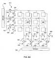
- FIG. 6Bis a block diagram depicting another mechanism for preventing the unselected conductive array lines from floating to an undesired voltage
- FIG. 6Cis a block diagram depicting an improvement on the mechanism for preventing the unselected conductive array lines from floating to an undesired voltage depicted in FIG. 6B ;
- FIG. 6Dis a block diagram depicting an improvement on the mechanism for preventing the unselected conductive array lines from floating to an undesired voltage depicted in FIG. 6C ;
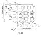
- FIG. 6Eis a block diagram depicting yet another mechanism for preventing the unselected conductive array lines from floating to an undesired voltage by using a 3-output driver;
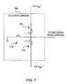
- FIG. 7is a block diagram depicting one possible configuration of a 3-output driver
- FIG. 8Ais a graph illustrating exemplary RV characteristics of a memory element initially biased in one direction
- FIG. 8Bis a graph illustrating exemplary RV characteristics of a memory element initially biased in the other direction
- FIG. 9is an exemplary flow chart of various processing steps that could be involved in a cross point array.
- FIG. 10is an exemplary memory cell that is formed using the processing steps in a side view.
- FIG. 1depicts an exemplary cross point array 100 .
- a bottom layer of x-direction conductive array lines 105 and a top layer of y-direction conductive array lines 110sandwiches a plurality of memory plugs 115 .
- the conductive array lines 105 and 110are arranged in the cross point array 100 so that each individual memory plug is capable of being uniquely identified and, therefore, uniquely selected by a single x-direction conductive array line and a single y-direction conductive array line.
- Conductive array lines 105 and 110can be constructed of any conductive material, such as aluminum, copper, tungsten or certain ceramics. Ideally, the material will withstand a high-temperature fabrication process, have a low inherent resistance, and have a low cost. Often, however, compromises will have to be made.
- the memory elementis a CMO
- very high temperaturesmight be required to form a polycrystalline or a single crystalline structure.
- the fabrication temperaturemight require that refractory metals be used for conductive array lines.
- refractive array lineshave higher resistances, which means that a given x-direction conductive array line would not be able to timely access as many y-direction conductive array lines as a lower resistance conductive array line, reducing the number of memory cells on the cross-point array 100 .
- a conductive array linewould cross between 64 and 8192 perpendicular conductive array lines.
- the x-direction and y-direction conductive array linescan be of equal lengths (forming a square cross point array) they can also be of unequal lengths (forming a rectangular cross point array).
- Each memory plug in the plurality of memory plugs 115contains a memory element along with any other materials that may be necessary, such as an insulating layer in an MRAM or a seed layer in a CMO.
- a CMO memory plugwould preferably include a non-ohmic device, as is described in co-pending application “High Density NVRAM,” U.S. application Ser. No. 10/360,005, filed Feb. 7, 2003.
- the non-ohmic deviceexhibits a very high resistance regime for a certain range of voltages (VNO ⁇ to VNO+) and a very low resistance regime for voltages above and below that range.
- FIG. 2depicts a side view of an exemplary memory plug 205 with seven separate thin-film layers and sandwiched between two conductive array lines 210 and 215 .
- the seven layersare: an electrode layer 220 , a layer of CMO material 225 (providing the memory element), another optional electrode layer 230 , three layers that make up a metal-insulator-metal (MIM) structure 235 , 240 and 245 (providing the non-ohmic device), and an optional final electrode 250 .
- MIMmetal-insulator-metal
- electrode layers 220 , 230 and 250are only necessary to the extent fabrication methods require them. Therefore, electrode layers 220 , 230 and 250 would ideally be as thin as possible while still preventing metal inter-diffusion and, if necessary, being useful as a seed layer.
- Typical electrode layers 220 , 230 and 250 commonly used in fabricationinclude Pt, Au, Ag and Al. If the electrode layers 220 , 230 and 250 are used only as a barrier to prevent metal inter-diffusion, then a thin layer of metal, e.g. TiN, could be used. Any number of electrically conductive materials can be used for CMO material's 225 seed layer 220 .
- the seed layer 220could be a conductive perovskite, such as LaNiO 3 or SrRuO 3 on Pt, a conductive metal oxide, such as IrO 2 on Ir or RuO 2 on Ru, a noble metal such as Pt on TiN.
- the other electrode layers 230 and 250could use the same conductive layer that was used on the seed layer 220 .
- the CMO material 225 thicknessis dictated by the desired resistive states of the CMO material 225 and the write threshold voltage (V Wth ). Although very dramatic differences (e.g., 1000 times difference) between a low resistance state (R 1 ) and a high resistive state (R 0 ) could be sensed very easily, the voltage that drives such resistances would be less than ideal. Since large currents can be destructive to semiconductors fabricated to small dimensions, no more than 10 ⁇ A would be desired for a memory circuit in most cases. Therefore, a modest difference between R 0 and R 1 would typically be a better choice.
- V Rread voltage
- R 1might be about 100 k ⁇ and R 0 might be about 1M ⁇ , making the current either 10 ⁇ A or 1 ⁇ A, depending on the resistive state.
- V Wa desired write voltage
- V Wshould be greater than V Wth for the same reason.
- a typical V Wmight be about 2 volts, and V Wth might be about 1.5 volts.
- a CMO material 225 with a V Wth of 1.5 voltsmight be between 1000 ⁇ and 3000 ⁇ thick.
- the CMO material 225will generally be a crystalline or polycrystalline perovskite structure.
- the CMO material 225includes two or more metals, the metals being selected from the group consisting of transition metals, alkaline earth metals and rare earth metals.
- the CMO material 225can be any number of compositions, including manganites (e.g., Pr 0.7 Ca 0.3 MnO 3 , Pr 0.5 Ca 0.5 MnO 3 and other PCMOs, LCMOs, etc.), titanites (e.g., STO:Cr), zirconates (e.g., SZO:Cr, Ca 2 Nb 2 O 7 :Cr, and Ta 2 O 5 :Cr), and high Tc superconductors (e.g., YBCO).
- manganitese.g., Pr 0.7 Ca 0.3 MnO 3 , Pr 0.5 Ca 0.5 MnO 3 and other PCMOs, LCMOs, etc.
- titanitese.g., STO:Cr
- zirconatese.g., SZO:Cr, Ca 2 Nb 2 O 7 :Cr, and Ta 2 O 5 :Cr
- high Tc superconductorse.g., YBCO
- MnO 3when combined with the rare earth metals La, Pr or some combination thereof and the alkaline earth metals Ca, Sr or some combination thereof have been found to produce a particularly effective CMO material 225 for use in a memory plug 205 .
- FIG. 3illustrates selection of a cell in the cross point array 100 .
- the point of intersection between a single x-direction conductive array line 305 and a single y-direction conductive array line 310uniquely identifies a single memory plug 315 .
- the selected conductive array lines 305 and 310deliver a voltage to every memory plug associated with those conductive array lines. Therefore, the non-ohmic device must be able to block current of the maximum voltage that will be seen on a single conductive array line but pass current from the minimum voltage seen on a selected memory plug.
- V W ′is V W plus all other voltage drops in the memory plug 315 (e.g., V NO+ ) and V R ′ is V R plus all other voltage drops in the memory plug 315 .
- a V NO+ of 2Vwould cause V W ′ to be 4V and V R ′ to be 3V.
- the thickness of the non-ohmic devicee.g., MIM 235 , 240 and 245 ) can be calculated.
- FIG. 4illustrates exemplary IV characteristics of a memory plug.
- the metal portion 235 and 245 of the MIMcan be made of any conductive material. However, to make fabrication more efficient, the metal portion 235 and 245 of the MIM could use the same conductive layer that was used with the seed layer 220 . Therefore, metal layers 235 and 245 of the MIM could also serve as the electrode layers 230 and 250 , removing the need to have a separate electrode layers 230 and 250 .
- the insulator layer 240 of the MIMcan be realized with Ta 2 O 5 , an amorphous SiC layer, or other such materials.
- Non-ohmic deviceincludes at least two oppositely oriented diodes.
- the oppositely oriented diodescan be connected either in series or in parallel.
- multiple diodescould be used in a diode ring formation in order to have an appropriate forward bias voltage drop. For example, if each diode where to have a forward bias voltage drop of 0.7V, placing two diodes in series oriented in the same direction would produce a total forward bias voltage drop of 1.4V. Similarly, a chain of two diodes in parallel with and oppositely oriented to the previous two diodes would cause the entire non-ohmic device to exhibit a high resistance from ⁇ 1.4V to +1.4V.
- the above-described voltagesare voltages seen by the memory plug 315 , and not necessarily the absolute values of the voltages from ground. For example, placing 10 volts on the selected x-direction conductive array line 305 and 6 volts on the selected y-direction conductive array line 310 would still attain a 4-volt drop. If the voltage drop across any single unselected memory plug was to be no more than 3 volts, then unselected conductive array lines 320 , 325 , 330 , 335 and 340 would need to be held somewhere between 7 volts and 9 volts in the above example.
- the unselected conductive array lines 320 , 325 , 330 , 335 and 340would be held at a constant voltage, regardless of whether a read or write operation was being performed. Therefore, if the selected x-direction conductive array line 310 were placed at 12 volts, then the y-direction unselected conductive array lines 320 and 325 would need to be held at 9 volts in the above example in order to keep the maximum voltage drop to 3 volts.
- a write operationmight require the x-direction conductive array line 310 be held to 11 volts, the y-direction conductive array line 305 be held to 5 volts and all the unselected conductive array lines 320 , 325 , 330 , 335 and 340 be held to 8 volts (halfway between the voltages of the two conductive array lines 305 and 310 for both read and write operations).
- each conductive array line 305 , 310 , 320 , 325 , 330 , 335 and 340is associated with a pass device 505 , 510 , 515 , 520 , 525 , 530 and 535 (one n-type and one p-type transistor).
- the gate voltages of each transistorare adjusted such that the selected conductive array lines 305 and 310 are allowed to pass a voltage from the drivers 540 .
- the voltage that is passedcan either be the full voltage from the drivers 540 during a write operation (a magnitude of 3 volts in the above example) in a first select mode, a partial voltage during a read operation (a magnitude of 2 volts in the above example) in a second select mode, or no voltage for the unselected lines in an unselect mode. Therefore, the pass devices 505 can act as part of the decoding circuitry as a type of modulating circuit, allowing one conductive array line to be on (“selected”) at either a read or write voltage and the other conductive array lines to be off (“unselected”).
- FIG. 5Aillustrates the logical connections and FIG. 5B illustrates the same connections, but with a different physical layout (the pass devices alternating on each end of the conductive array lines).
- a single transistorin place of the pass device 505 , 510 , 515 , 520 , 525 , 530 and 535 , a single transistor can be used.
- the transistor's gate voltagewould need to be such that it could pass large magnitude voltages.
- an n-channel transistorwould pass the full 3V if its gate were held to 3V plus the n-channel transistor's threshold voltage.
- a single transistorcould still act as a modulating circuit by only partially turning on the transistor.
- the modulationis performed upstream of the gate circuit. Regardless of whether the gate circuit is a pass device or a single transistor, the input to the gate circuit would already be at an appropriate read or write voltage. In this embodiment, the gate circuit would only have a first select mode (passing substantially the full input voltage) and an unselect mode (passing substantially no voltage).
- the unselected conductive array lines 320 , 325 , 330 , 335 and 340were not held to a certain voltage, they would be considered floating, which is generally discouraged in circuit design. Specifically, a problem would arise if, for example, an unselected y-direction conductive array line 340 were floating at ⁇ 3 volts. If the selected x-direction conductive array line 305 was at 3 volts and the selected y-direction conductive array line 310 was at ⁇ 3 volts, two cells 315 and 545 would see a 6-volt drop, potentially disturbing the resistive states of both cells.
- FIG. 6Aillustrates one mechanism for preventing the unselected conductive array lines 320 , 325 , 330 , 335 and 340 from floating to an undesired voltage.
- each pass device 505 , 510 , 515 , 520 , 525 , 530 and 535would have both of their transistors turned on, the drivers 540 would be deactivated, and voltage reference generators 605 would be at some reference voltage (presumed to be ground for the remainder of this document). Therefore, all the conductive array lines 305 , 310 , 320 , 325 , 330 , 335 and 340 would be pulled to the reference voltage.
- the voltage reference generator 605would be deactivated, the driver 540 would be activated, and only the appropriate pass devices 505 and 510 would be on, bringing the selected conductive array lines 305 and 310 to the driver voltage.
- the unselected conductive array lines 320 , 325 , 330 , 335 and 340would be floating during a read or write operation, their parasitic capacitance might keep them at the reference voltage for the time it takes to do a normal read or write cycle. However, lateral coupling capacitance will work against the parasitic capacitance, raising the voltage on the unselected conductive array lines 320 , 325 , 330 and 335 adjacent to the selected conductive array lines 305 and 310 .
- FIG. 6Billustrates another mechanism for preventing the unselected conductive array lines 320 , 325 , 330 , 335 and 340 from floating to an undesired voltage.
- Each conductive array line 305 , 310 320 , 325 , 330 , 335 and 340would have an associated grounding pass device 610 , 615 , 620 , 625 , 630 , 635 and 640 that allows the conductive array lines 305 , 310 320 , 325 , 330 , 335 and 340 to be pulled to ground when activated.
- the grounding pass devices 610 , 615 , 620 , 625 , 630 , 635 and 640could be activated prior to a read or write operation (similar to the operation described in connection with FIG. 6A ), could be triggered by the selection of a conductive array line, or could always be kept on. If the grounding pass devices 610 , 615 , 620 , 625 , 630 , 635 and 640 were always on, their relative size would need to be small in relation to the decoding pass devices 505 , 510 , 515 , 520 , 525 , 530 and 535 so that the leakage to ground would have a small effect.
- grounding pass devices 610 , 615 , 620 , 625 , 630 , 635 and 640were triggered by the selection of a conductive array line, the process of selecting the x-direction conductive array line 305 , would activate the decoding pass device 505 and deactivate the grounding pass device 610 associated with the selected conductive array line 305 while deactivating the decoding pass devices 515 and 520 and activating the grounding pass devices 635 and 640 associated with the unselected conductive array lines 320 and 325 .
- selecting the y-direction conductive array line 310would activate the decoding pass device 510 and deactivate the grounding pass device 615 associated with the selected conductive array line 310 while deactivating the decoding pass devices 525 , 530 and 535 and activating the grounding pass devices 620 , 625 and 630 associated with the unselected conductive array lines 330 , 335 and 340 .
- FIG. 6Cis an improvement on FIG. 6B .
- a single transistor 645 , 650 , 655 , 660 , 665 , 670 and 675is used instead of pass devices 610 , 615 , 620 , 625 , 630 , 635 and 640 .
- the transistors 645 , 650 , 655 , 660 , 665 , 670 and 675were n-channel devices, they would be on only if the gate voltage were held to at least the threshold voltages of the transistors.
- the transistorswere p-channel devices, they would be on if the gate voltages were held to at least the negative threshold voltages. Therefore, an appropriate gate voltage can fully discharge the conductive array lines.
- the single n-channel (or p-channel) transistor embodimentcan be used either at the beginning of a cycle or by using the inverse of the signal that activates the n-channel (or p-channel) portion of the decoding pass devices 505 , 510 , 515 , 520 , 525 , 530 and 535 .
- the inverse signalmight simply be the p-channel (or n-channel) portion of the decoding pass devices 505 , 510 , 515 , 520 , 525 , 530 and 535 .
- FIG. 6Eillustrates yet another mechanism for preventing the unselected conductive array lines 320 , 325 , 330 , 335 and 340 from floating to an undesired voltage by using a 3-output driver 680 .
- the 3-output driver 680would deliver a voltage to all of the decoding pass devices 505 , 510 , 515 , 520 , 525 , 530 and 535 , such a mechanism could not be used while a specific conductive array line was being selected. Therefore, the 3-output driver 680 could either be used to discharge the floating voltages prior to a read or write operation. Alternatively, the 3-output driver 680 could be used during a read or write operation if it were only used in connection with unselected banks, assuming multiple 3-output drivers 680 are used for multiple banks.
- FIG. 7illustrates one possible configuration of a 3-output driver 680 .
- a p-channel transistor 705 and an n-channel transistor 710are arranged in series.
- the n-channel transistormay be in a separate well from the CMOS logic because the substrate is tied to a negative voltage.
- the source of the p-channel transistor 705is connected to a voltage source of +1 ⁇ 2 V W ′ and the source of the n-channel transistor 710 is connected to a voltage source of ⁇ 1 ⁇ 2 V W ′.
- the drains of both transistorsare connected to both the decoding pass devices 505 , 510 , 515 , 520 , 525 , 530 and 535 and transistor to ground 815 .
- the transistor to ground 715would need to have an appropriate gate voltage, as described in connection with FIG. 6C , or be a pass device.
- the 3-output driver 680would function when only one transistor 705 , 710 or 715 was on, while the other two transistors were off.
- the driver 540 or the 3-output driver 680must be able to supply either +1 ⁇ 2 V W ′ or ⁇ 1 ⁇ 2 V W ′ to the decoding pass devices 505 , 510 , 515 , 520 , 525 , 530 and 535 .
- the polarity of the voltage dropis not important during a read.
- the resistive state of the memory elementcan be detected regardless of whether the x-direction conductive array line 305 is V R ′ higher or V R ′ lower than the y-direction conductive array line 310 . However, it is probably desirable to alternate polarities of reads so the memory elements will not be subjected to any long-term read disturbs.
- a write operationwould usually be preceded by a read operation in order to ensure a write is necessary.
- +V W ′should only be applied to a memory plug in its R 0 resistive state and ⁇ V W ′ should only be applied to a memory plug in its R 1 resistive state.
- the CMO material 225would not either be placed in a resistive state lower than R 1 or higher than R 0 or suffer any degradation that occurs with certain CMO materials.
- avoiding a write operationwill reduce disturbing the unselected cells and improve the endurance of the selected cell, avoiding unnecessarily stressing the cross point memory array 100 .
- the polarity of the readshould be the same as the polarity of the write operation that would follow, if required. For example, if the data to be written is “0” then the selected x-direction conductive array line 305 would be 3V and the selected y-direction conductive array line 310 would be ⁇ 3V. If the read operation preceding the write used +2V on the selected x-direction conductive array line 305 and ⁇ 2V on the selected y-direction conductive array line 310 , then the circuitry would only need to switch 1V for both conductive array lines 305 and 310 . This can be preferable to the alternative ( ⁇ 2V on the selected x-direction conductive array line 305 and +2V on the selected y-direction conductive array line 310 ), which would require the voltage to switch a total of 5V.
- the ability of the CMO material 225 to be placed into several different resistive statescan be exploited to store more than one bit of information per memory plug 205 .
- multiple resistive statescan be used.
- the CMO material 225might have a high resistive state of R 00 , a medium-high resistive state of R 01 , a medium-low resistive state of R 10 and a low resistive state of R 11 .
- a sensitive reading mechanismmight be able to distinguish between three or more bits of information contained in the CMO material 225 .
- a benefit of some CMO materialsis that the characteristic hysteresis allows non-destructive reads. As shown in FIG. 8A any voltages between ⁇ V R ( ⁇ 1 volt) and +V R (1 volt) will have no effect on the resistive state of the memory element (i.e., it will remain at either 100 k ⁇ or 1M ⁇ ). Therefore, a write operation is not necessary after a read operation for such materials.
- the hysteresishas two write threshold voltages, one for when the CMO material 225 is in the low resistive state and one for when the CMO material 225 is in the high resistive state.
- the first write threshold voltageis the point above which any voltages applied across the CMO material 225 have substantially no effect on the resistive state of the CMO material 225 and below which a voltage pulse will alter the resistance of the CMO material 225 .
- the second write threshold voltageis the point below which any voltages applied across the CMO material 225 have substantially no effect on the resistive state of the CMO material 225 and above which a voltage pulse will alter the resistance of the CMO material 225 .
- the CMO material 225When initially fabricated, the CMO material 225 may be in a high resistive state. The CMO material 225 then transitions from its high resistive state to a low resistive state in response to a voltage pulse. Whether the x-direction conductive array line 305 is at +3V and the y-direction conductive array line 310 is at ⁇ 3V in order to lower the resistive state or vice-versa depends upon the specific properties of the material that is used.
- FIG. 8Ais an example of the CMO material 225 that requires a +2V pulse to lower its resistive state
- FIG. 8Ba mirror image of FIG. 8A , is an example of the CMO material 225 that requires a ⁇ 2V pulse to lower its resistive state.
- the actual write voltage that is used on the CMO material 225is greater in magnitude than the write threshold voltage.
- the actual write voltageis a voltage pulse that would place the CMO material 225 into the desired resistive state, which may be lower than the highest physically attainable resistive state and higher than the lowest attainable resistive state.
- the appropriate write voltage for the previously described exemplary CMO material 225is ⁇ 2V when it is in its low resistive state and 2V when it is in its high resistive state.
- the CMO material 225should switch very quickly from one resistive state to another. For current applications, anything less than 50 nanoseconds would be an appropriate switching speed. Additionally, once the CMO material 225 is placed in a resistive state, it should be able to retain that state for long periods of time. Ideally, the material should retain its resistive state for over ten years. Since the read voltage should not affect the resistive state, repeated application of the read voltage over ten years should not change the resistive state of the CMO material 225 .
- the chemical and materials properties of the memory elementare selected to meet the electrical specifications set forth above.
- the materialpreferably has a resistivity of not greater than about 1 ohm-cm, exhibits a change in resistance of at least about 10 ⁇ , and has this resistance change triggered by the application of a voltage pulse of not longer than about 100 ns duration and not greater than about than 3V in magnitude.
- the memory element materialshould be compatible with the requirements imposed by the general fabrication process of the entire high density RAM. Of course, there is some flexibility in the process constraints. Thus, process and design engineers will have certain ranges of chemical, materials, and process parameters available to tailor for the specific goals at hand. Among these parameters are the annealing conditions, the deposition temperature and method, and the material stoichiometry and the thickness.
- the memory element materialshould have a resistivity of not more than about 1 ohm-cm. It is known that the resistivity of the complex metal oxides depends upon various factors, often including some of the following: film thickness, oxygen content of the film, stoichiometry, elemental composition, deposition method and conditions, degree of crystallinity, crystallite size, crystalline orientation, and doping level and choice of dopant. Current research indicates that suitably low resistivity (less than or equal to 1 ohm-cm) CMO materials can be achieved by judicious choice of these parameters.
- One example of a suitable film thickness for the memory applications of this inventionis approximately 100 ⁇ to 3000 ⁇ . Thinner films sometimes have higher strains, usually resulting from a slight misalignment with the seed layer, which can result in higher resistivity. Film thickness has been discussed by S. I. Khartsev, et al. in “Colossal magnetoresistance in ultrathin epitaxial La 0.75 Sr 0.25 MnO 3 films,” Journal of Applied Physics, Vol. 87, No. 5, 1 Mar. 2000, which is hereby incorporated by reference for all purposes.
- some specific CMO materials suitable for use with this inventionwill have the following properties: (1) the thickness of the deposited complex metal oxide film is between 1000 ⁇ and 3000 ⁇ ; (2) the deposition and cool down and post deposition annealing (if any) is performed in an oxygen rich ambient; (3) the ratio of the rare earth and alkaline earth metals is adjusted for lowest resistivity, e.g., about 0.5; (4) the material is deposited or annealed to give a polycrystalline structure; (5) the material is deposited or annealed to increase the percentage of crystallites in a preferred orientation; and (6) the CMO material is doped with a material that has the effect of pinning the oxygen vacancies. Regarding the last property, it has been found that a small percentage of chrome doping also has a beneficial effect on reliability and endurance of some CMO films.
- the seed layer or other “substrate” on which the CMO depositsimpacts the resistivity of the CMO and other properties.
- the underlying crystrallographic orientation of the substratewill epitaxially propagate to the upper levels the CMO element. So, for example, if the underlying substrate has a 100 orientation, then the CMO may preferentially deposit in a 100 orientation.
- the underlying substrateis a conductive electrode such a noble metal (e.g., platinum) or relatively conductive CMO such as LaNiO 3 .
- suitable crystallite sizesmay range from about 100 ⁇ to about 500 ⁇ .
- the general process operations for creating a complex metal oxide memory elementinclude (1) providing a substrate on which to directly form the memory element, (2) depositing the memory element material on the substrate, and optionally (3) post-processing the deposited material to impart a desired property.
- the substrate materialshould be polycrystalline or single crystalline, be conductive, and serve as an electrode.
- PVDphysical vapor deposition
- CVDchemical vapor deposition
- thin-film processessuch as facing target sputtering and laser annealing after deposition might allow for the formation of a crystalline memory element at temperatures low enough to use copper or aluminum conductive array lines
- most thin-film processeswould require temperatures of about 600° C. to form crystalline memory elements. Therefore, any layers of conductive array lines underneath the memory elements would need to withstand those temperatures.
- FIG. 9is an exemplary flow chart of various processing steps that could be involved in a W cross point array.
- FIG. 10is an elevation view of a cell 1000 formed with the processing steps.
- FEOLfront end of line
- FEOL processesare generally defined as operations performed on a semiconductor wafer in the course of device manufacturing up to first metallization, and might end with chemical-mechanical polishing (CMP) of an inter-layer dielectric (ILD) 1002 , such as SiO 2 .
- CMPchemical-mechanical polishing
- ILDinter-layer dielectric
- the next processing step at 910is formation of contact holes through the ILD 1002 to appropriate positions in the circuitry followed by W plug 1005 formation at 915 .
- a barrier/adhesion layer 1010 of 100 ⁇ of Ti followed by 200 ⁇ of TiNcould be sputtered on the wafer, followed by 5000 ⁇ of W deposited using CVD, followed by etchback or CMP to remove W on the ILD surface 1002 , leaving W plugs 1005 in the contact holes.
- the W conductive array lines 1020are patterned on the wafer at 920 . Since W has a relatively high resistivity, the maximum length and minimum cross-sectional area may be limited in comparison to aluminum or copper. Specifically, the maximum length and cross-sectional area of the conductive array lines 1020 can be determined using Error! Objects cannot be created from editing field codes and setting a maximum resistance to about 10 k ⁇ in order to maintain fast access times. Assuming 5000 ⁇ thick metallization layers and a feature size of 0.25 cm, the length of the conductive array lines 1020 would be a maximum of about 2000 ⁇ m long.
- the W conductive array lines 1020can be achieved through a barrier/adhesion layer 1015 of 100 ⁇ of Ti plus 200 ⁇ of TiN, followed by 5000 ⁇ of W deposition through CVD, followed by mask, etch, and resist strip steps.
- the dielectric layer 1025can be a thick layer of SiO 2 , deposited over the W conductive array lines 1020 by plasma-enhanced chemical vapor deposition (PECVD) and then planarized by CMP to expose the top surfaces of the W lines 1020 .
- PECVDplasma-enhanced chemical vapor deposition
- the bottom electrodes 1030are deposited.
- a 500 ⁇ thick barrier layer of TiNis deposited to prevent metal inter-diffusion, followed by a 200 ⁇ seed layer of LaNiO 3 (LNO) or SrRuO 3 (SRO). These layers can be deposited by sputtering.
- LNOLaNiO 3
- SROSrRuO 3
- step 935approximately 2000 ⁇ of memory material 1035 having a stoichiometry of Pr 0.7 Ca 0.3 MnO 3 is deposited at about 600° C. by a physical vapor deposition technique such as sputtering. As previously explained, the memory element 1035 would have a low resistance of 100 k Ohm and a high resistance of 1M Ohm, and would change state with a less than 50 ns flat pulse at 2V. At 940 another electrode 1040 (200 ⁇ of LNO or SRO and another 500 ⁇ of TiN are deposited via sputtering) is deposited on top of the memory element 1035 .
- the non-ohmic device 1045is formed.
- the device 1045can be formed by first sputtering 250 ⁇ of Al, followed by 50 ⁇ of Al 2 O 3 , and another 250 ⁇ of sputtered Al.
- the Al 2 O 3could be formed by atomic layer deposition (ALD) or oxidization of Al.
- ALDatomic layer deposition
- the Al 2 O 3 thicknesswould be chosen to achieve a V NO+ of 4V.
- another 500 ⁇ barrier layer 1050 of sputtered TiNis optionally deposited in step 955 to prevent metal inter-diffusion.
- via holesare formed. Via holes with W plugs could be formed to provide connections between metal interconnect layers. Standard photolithography and via etch could be used to make via holes. These via holes could be filled by depositing 100 ⁇ of Ti, followed by 200 ⁇ of TiN, followed by a 5000 ⁇ W layer. CMP could then be used to remove W on the ILD surface 1060 , leaving the W plugs in the via holes.
- the final layer of conductive array linesmay comprise aluminum, copper or other high conductivity metal.
- a top layer of conductive array linescould then be formed at 980 by depositing, in order, another barrier/adhesion layer 1065 of 100 ⁇ of Ti and 200 ⁇ of TiN, then the conductive array line 1070 comprising 5000 ⁇ of an Al/Cu mixture, and then a final barrier/adhesion layer 1075 of 100 ⁇ of Ti, 200 ⁇ of TiN.
- An anti-reflective coating (ARC) 1080such as SiON could also be deposited.
- a final mask, etch and resist stripwould then be performed.
- the final cross-point memory arraycould then be 16384 W conductive array lines by 4096 Al/Cu conductive array lines to create a 64Mbit array. 16 of these arrays could be laid side-by-side to create a 1 Gbit memory.
- memory elementsare formed by a high temperature process that could be incompatible with conventional aluminum and copper deposition processes.
- Other processes for forming memory elements at low temperaturesexist. These include facing target sputtering and laser annealing.
Landscapes
- Engineering & Computer Science (AREA)
- Power Engineering (AREA)
- Chemical & Material Sciences (AREA)
- Materials Engineering (AREA)
- Computer Hardware Design (AREA)
- Semiconductor Memories (AREA)
Abstract
Description
- This application is a continuation of U.S. patent application Ser. No. 10/330,170, filed on Dec. 26, 2002, now U.S. Pat. No. 6,970,375, which claims the benefit of U.S. Provisional Application No. 60/400,849, filed Aug. 02, 2002, the U.S. Provisional Application No. 60/422,922, filed Oct. 31, 2002, and the U.S. Provisional Application 60/424,083, filed Nov. 5, 2002, all of which are incorporated herein by reference in their entireties and for all purposes.
- 1. Field of the Invention
- The present invention relates generally to memory, and more specifically to memory employing a cross point array.
- 2. Description of the Related Art
- Conventional nonvolatile memory requires three terminal MOSFET-based devices. The layout of such devices are not ideal, usually requiring feature sizes of 8 f2for each memory cell, where f is the minimum feature size.
- However, not all memory elements require three terminals. Certain complex metal oxides (CMOs), for example, can retain a resistive state after being exposed to an electronic pulse, which can be generated from two terminals. U.S. Pat. No. 6,204,139, issued Mar. 20, 2001 to Liu et al., incorporated herein by reference for all purposes, describes some perovskite materials that exhibit such characteristics. The perovskite materials are also described by the same researchers in “Electric-pulse-induced reversible resistance change effect in magnetoresistive films,” Applied Physics Letters, Vol. 76, No. 19, 8 May 2000, and “A New Concept for Non-Volatile Memory: The Electric-Pulse Induced Resistive Change Effect in Colossal Magnetoresistive Thin Films,” in materials for the 2001 Non-Volatile Memory Technology Symposium, all of which are hereby incorporated by reference for all purposes.
- Similarly, the IBM Zurich Research Center has also published three technical papers that also discuss the use of metal oxide material for memory applications: “Reproducible switching effect in thin oxide films for memory applications,” Applied Physics Letters, Vol. 77, No. 1, 3 Jul. 2000, “Current-driven insulator-conductor transition and nonvolatile memory in chromium-doped SrTiO3single crystals,” Applied Physics Letters, Vol. 78, No. 23, 4 Jun. 2001, and “Electric current distribution across a metal-insulator-metal structure during bistable switching,” Journal of Applied Physics, Vol. 90, No. 6, 15 Sep. 2001, all of which are hereby incorporated by reference for all purposes.
- Similarly, magnetic RAM (MRAM) requires only two terminals to deliver a magnetic field to the memory element. Other two terminal devices include Ovonic Unified Memory (OUM), which uses chalcogenic layers of material, and various types of ferroelectric memory. With only two terminals, it has been theorized that memory can be arranged in a cross point architecture.
- However, mere recognition that a two terminal memory element is theoretically capable of being placed in a cross point array does not solve many of the non-trivial problems associated with actually creating such a device.
- The invention may best be understood by reference to the following description taken in conjunction with the accompanying drawings, in which:
FIG. 1 depicts an exemplary cross point memory array in a perspective view;FIG. 2 depicts an exemplary memory plug in contact with two conductive array lines in a side view;FIG. 3 depicts the exemplary cross point memory array in a plan view;FIG. 4 is a graph illustrating exemplary IV characteristics of a memory plug;FIG. 5A is a block diagram depicting the logical connections of various systems that contribute to selecting a memory plug;FIG. 5B is a block diagram depicting the physical connections of the various systems that contribute to selecting a memory plug;FIG. 6A is a block diagram depicting one mechanism for preventing the unselected conductive array lines from floating to an undesired voltage;FIG. 6B is a block diagram depicting another mechanism for preventing the unselected conductive array lines from floating to an undesired voltage;FIG. 6C is a block diagram depicting an improvement on the mechanism for preventing the unselected conductive array lines from floating to an undesired voltage depicted inFIG. 6B ;FIG. 6D is a block diagram depicting an improvement on the mechanism for preventing the unselected conductive array lines from floating to an undesired voltage depicted inFIG. 6C ;FIG. 6E is a block diagram depicting yet another mechanism for preventing the unselected conductive array lines from floating to an undesired voltage by using a 3-output driver;FIG. 7 is a block diagram depicting one possible configuration of a 3-output driver;FIG. 8A is a graph illustrating exemplary RV characteristics of a memory element initially biased in one directionFIG. 8B is a graph illustrating exemplary RV characteristics of a memory element initially biased in the other direction;FIG. 9 is an exemplary flow chart of various processing steps that could be involved in a cross point array; andFIG. 10 is an exemplary memory cell that is formed using the processing steps in a side view.- It is to be understood that, in the drawings, like reference numerals designate like structural elements. Also, it is understood that the depictions in the figures are not necessarily to scale.
FIG. 1 depicts an exemplarycross point array 100. A bottom layer of x-directionconductive array lines 105 and a top layer of y-directionconductive array lines 110 sandwiches a plurality ofmemory plugs 115. Theconductive array lines cross point array 100 so that each individual memory plug is capable of being uniquely identified and, therefore, uniquely selected by a single x-direction conductive array line and a single y-direction conductive array line.Conductive array lines - For example, if the memory element is a CMO, very high temperatures might be required to form a polycrystalline or a single crystalline structure. Depending upon the fabrication process (e.g., solution based spin on followed by high temperature anneal, pulsed laser deposition, sputtering, and metalorganic chemical vapor deposition) the fabrication temperature might require that refractory metals be used for conductive array lines. However, refractive array lines have higher resistances, which means that a given x-direction conductive array line would not be able to timely access as many y-direction conductive array lines as a lower resistance conductive array line, reducing the number of memory cells on the
cross-point array 100. Therefore, compromises must be made in order to balance cost, size, resistivity and preferred fabrication techniques. Typically, a conductive array line would cross between 64 and 8192 perpendicular conductive array lines. Although the x-direction and y-direction conductive array lines can be of equal lengths (forming a square cross point array) they can also be of unequal lengths (forming a rectangular cross point array). - Each memory plug in the plurality of memory plugs115 contains a memory element along with any other materials that may be necessary, such as an insulating layer in an MRAM or a seed layer in a CMO. Additionally, a CMO memory plug would preferably include a non-ohmic device, as is described in co-pending application “High Density NVRAM,” U.S. application Ser. No. 10/360,005, filed Feb. 7, 2003. The non-ohmic device exhibits a very high resistance regime for a certain range of voltages (VNO− to VNO+) and a very low resistance regime for voltages above and below that range.
FIG. 2 depicts a side view of anexemplary memory plug 205 with seven separate thin-film layers and sandwiched between twoconductive array lines electrode layer 220, a layer of CMO material225 (providing the memory element), anotheroptional electrode layer 230, three layers that make up a metal-insulator-metal (MIM)structure final electrode 250.- The electrode layers220,230 and250 are only necessary to the extent fabrication methods require them. Therefore, electrode layers220,230 and250 would ideally be as thin as possible while still preventing metal inter-diffusion and, if necessary, being useful as a seed layer. Typical electrode layers220,230 and250 commonly used in fabrication include Pt, Au, Ag and Al. If the electrode layers220,230 and250 are used only as a barrier to prevent metal inter-diffusion, then a thin layer of metal, e.g. TiN, could be used. Any number of electrically conductive materials can be used for CMO material's225
seed layer 220. For example, theseed layer 220 could be a conductive perovskite, such as LaNiO3or SrRuO3on Pt, a conductive metal oxide, such as IrO2on Ir or RuO2on Ru, a noble metal such as Pt on TiN. To make fabrication more efficient, theother electrode layers seed layer 220. - The
CMO material 225 thickness is dictated by the desired resistive states of theCMO material 225 and the write threshold voltage (VWth). Although very dramatic differences (e.g., 1000 times difference) between a low resistance state (R1) and a high resistive state (R0) could be sensed very easily, the voltage that drives such resistances would be less than ideal. Since large currents can be destructive to semiconductors fabricated to small dimensions, no more than 10 μA would be desired for a memory circuit in most cases. Therefore, a modest difference between R0and R1would typically be a better choice. For example, if 1 volt were used as a read voltage (VR), R1might be about 100 kΩ and R0might be about 1MΩ, making the current either 10 μA or 1 μA, depending on the resistive state. Once a VRis identified, a desired write voltage (VW) can be determined. Not only should VWbe greater than VR, but it should also be far enough away from VRto allow minor voltage fluctuations (e.g., due to fabrication imperfections) to have a negligible effect on theCMO material 225. Similarly, VWshould be greater than VWthfor the same reason. A typical VWmight be about 2 volts, and VWthmight be about 1.5 volts. ACMO material 225 with a VWthof 1.5 volts might be between 1000 Å and 3000 Å thick. - The
CMO material 225 will generally be a crystalline or polycrystalline perovskite structure. Generally, theCMO material 225 includes two or more metals, the metals being selected from the group consisting of transition metals, alkaline earth metals and rare earth metals. TheCMO material 225 can be any number of compositions, including manganites (e.g., Pr0.7Ca0.3MnO3, Pr0.5Ca0.5MnO3and other PCMOs, LCMOs, etc.), titanites (e.g., STO:Cr), zirconates (e.g., SZO:Cr, Ca2Nb2O7:Cr, and Ta2O5:Cr), and high Tc superconductors (e.g., YBCO). Specifically, MnO3, when combined with the rare earth metals La, Pr or some combination thereof and the alkaline earth metals Ca, Sr or some combination thereof have been found to produce a particularlyeffective CMO material 225 for use in amemory plug 205. - The properties of the
MIM structure FIG. 3 illustrates selection of a cell in thecross point array 100. The point of intersection between a single x-directionconductive array line 305 and a single y-directionconductive array line 310 uniquely identifies asingle memory plug 315. However, the selectedconductive array lines conductive array line memory plug 315. - If the non-ohmic device is the only other element that causes a voltage drop, the minimum VNO+ can be calculated from VNO+=½ VW′=½ (VNO++VW)=VW). A VNO+ of 2V would cause VW′ to be 4V and VR′ to be 3V. However, a higher VNO+ might be appropriate to allow for some fabrication inconsistencies and other additional elements in the memory plug that provides a voltage drop. For example, with a VW=2V, a VNO+ of 4V would cause VW′ to be at least 6V and VR′ to be at least 4V. Once a VNO+ is selected, then the thickness of the non-ohmic device (e.g.,
MIM FIG. 4 illustrates exemplary IV characteristics of a memory plug. - The
metal portion metal portion seed layer 220. Therefore,metal layers separate electrode layers insulator layer 240 of the MIM can be realized with Ta2O5, an amorphous SiC layer, or other such materials. - Other structures that might be used for the non-ohmic device include at least two oppositely oriented diodes. The oppositely oriented diodes can be connected either in series or in parallel.
- When two diodes are in series, one diode's forward current is blocked by the other diode at low voltages. However, at the breakdown voltage of each diode, the resistance to current flow diminishes greatly. Hence, in this embodiment, it is the diodes' breakdown voltages that define VNO+ and VNO−.
- When the diodes are in parallel, multiple diodes could be used in a diode ring formation in order to have an appropriate forward bias voltage drop. For example, if each diode where to have a forward bias voltage drop of 0.7V, placing two diodes in series oriented in the same direction would produce a total forward bias voltage drop of 1.4V. Similarly, a chain of two diodes in parallel with and oppositely oriented to the previous two diodes would cause the entire non-ohmic device to exhibit a high resistance from −1.4V to +1.4V.
- Yet another structure that might be used was described in a paper called “A switching Device based on a-Si:H N-i-dp-i-n stacked structure: Modeling and characterization,” by Domenico Caputo and Giampiero de Cesare (IEEE Transactions on Electron Devices, Vol 43, No 12, December 1996), incorporated herein by reference for all purposes. The five layer structure described in the paper consists of an n-type silicon layer, an intrinsic silicon layer, a very thin p-type silicon layer, an intrinsic silicon layer and an n-type layer.
- Those skilled in the art will appreciate that the above-described voltages are voltages seen by the
memory plug 315, and not necessarily the absolute values of the voltages from ground. For example, placing 10 volts on the selected x-directionconductive array line 305 and 6 volts on the selected y-directionconductive array line 310 would still attain a 4-volt drop. If the voltage drop across any single unselected memory plug was to be no more than 3 volts, then unselectedconductive array lines - Preferably, the unselected
conductive array lines conductive array line 310 were placed at 12 volts, then the y-direction unselectedconductive array lines conductive array line 310 be held to 11 volts, the y-directionconductive array line 305 be held to 5 volts and all the unselectedconductive array lines conductive array lines - As illustrated in the preferred embodiment of
FIGS. 5A and 5B , eachconductive array line pass device conductive array lines drivers 540. The voltage that is passed can either be the full voltage from thedrivers 540 during a write operation (a magnitude of 3 volts in the above example) in a first select mode, a partial voltage during a read operation (a magnitude of 2 volts in the above example) in a second select mode, or no voltage for the unselected lines in an unselect mode. Therefore, thepass devices 505 can act as part of the decoding circuitry as a type of modulating circuit, allowing one conductive array line to be on (“selected”) at either a read or write voltage and the other conductive array lines to be off (“unselected”).FIG. 5A illustrates the logical connections andFIG. 5B illustrates the same connections, but with a different physical layout (the pass devices alternating on each end of the conductive array lines). - Alternatively, in place of the
pass device - In another embodiment, the modulation is performed upstream of the gate circuit. Regardless of whether the gate circuit is a pass device or a single transistor, the input to the gate circuit would already be at an appropriate read or write voltage. In this embodiment, the gate circuit would only have a first select mode (passing substantially the full input voltage) and an unselect mode (passing substantially no voltage).
- It should be noted that if the unselected
conductive array lines conductive array line 340 were floating at −3 volts. If the selected x-directionconductive array line 305 was at 3 volts and the selected y-directionconductive array line 310 was at −3 volts, twocells FIG. 6A illustrates one mechanism for preventing the unselectedconductive array lines pass device drivers 540 would be deactivated, andvoltage reference generators 605 would be at some reference voltage (presumed to be ground for the remainder of this document). Therefore, all theconductive array lines voltage reference generator 605 would be deactivated, thedriver 540 would be activated, and only theappropriate pass devices conductive array lines conductive array lines conductive array lines conductive array lines FIG. 6B illustrates another mechanism for preventing the unselectedconductive array lines conductive array line grounding pass device conductive array lines - The
grounding pass devices FIG. 6A ), could be triggered by the selection of a conductive array line, or could always be kept on. If thegrounding pass devices decoding pass devices - If the
grounding pass devices conductive array line 305, would activate thedecoding pass device 505 and deactivate thegrounding pass device 610 associated with the selectedconductive array line 305 while deactivating thedecoding pass devices grounding pass devices conductive array lines conductive array line 310 would activate thedecoding pass device 510 and deactivate thegrounding pass device 615 associated with the selectedconductive array line 310 while deactivating thedecoding pass devices grounding pass devices conductive array lines FIG. 6C is an improvement onFIG. 6B . However, instead ofpass devices single transistor transistors - The single n-channel (or p-channel) transistor embodiment can be used either at the beginning of a cycle or by using the inverse of the signal that activates the n-channel (or p-channel) portion of the
decoding pass devices FIG. 6D , in some embodiments, the inverse signal might simply be the p-channel (or n-channel) portion of thedecoding pass devices FIG. 6E illustrates yet another mechanism for preventing the unselectedconductive array lines output driver 680. Since the 3-output driver 680 would deliver a voltage to all of thedecoding pass devices output driver 680 could either be used to discharge the floating voltages prior to a read or write operation. Alternatively, the 3-output driver 680 could be used during a read or write operation if it were only used in connection with unselected banks, assuming multiple 3-output drivers 680 are used for multiple banks.FIG. 7 illustrates one possible configuration of a 3-output driver 680. A p-channel transistor 705 and an n-channel transistor 710 are arranged in series. The n-channel transistor may be in a separate well from the CMOS logic because the substrate is tied to a negative voltage. The source of the p-channel transistor 705 is connected to a voltage source of +½ VW′ and the source of the n-channel transistor 710 is connected to a voltage source of −½ VW′. The drains of both transistors are connected to both thedecoding pass devices FIG. 6C , or be a pass device. The 3-output driver 680 would function when only onetransistor - Depending on the embodiment, the
driver 540 or the 3-output driver 680, must be able to supply either +½ VW′ or −½ VW′ to thedecoding pass devices CMO material 225 from R0to R1and applying a pulse of VW′ in the opposite direction (−VW′) will increase the resistive state from R1to R0. - The polarity of the voltage drop is not important during a read. The resistive state of the memory element can be detected regardless of whether the x-direction
conductive array line 305 is VR′ higher or VR′ lower than the y-directionconductive array line 310. However, it is probably desirable to alternate polarities of reads so the memory elements will not be subjected to any long-term read disturbs. - Additionally, a write operation would usually be preceded by a read operation in order to ensure a write is necessary. In other words, +VW′ should only be applied to a memory plug in its R0resistive state and −VW′ should only be applied to a memory plug in its R1resistive state. By ensuring that a voltage pulse is only used when the
CMO material 225 needs to change state, theCMO material 225 would not either be placed in a resistive state lower than R1or higher than R0or suffer any degradation that occurs with certain CMO materials. Additionally, avoiding a write operation will reduce disturbing the unselected cells and improve the endurance of the selected cell, avoiding unnecessarily stressing the crosspoint memory array 100. - If a read operation is used prior to a write operation, the polarity of the read should be the same as the polarity of the write operation that would follow, if required. For example, if the data to be written is “0” then the selected x-direction
conductive array line 305 would be 3V and the selected y-directionconductive array line 310 would be −3V. If the read operation preceding the write used +2V on the selected x-directionconductive array line 305 and −2V on the selected y-directionconductive array line 310, then the circuitry would only need to switch 1V for bothconductive array lines conductive array line 305 and +2V on the selected y-direction conductive array line310), which would require the voltage to switch a total of 5V. - The ability of the
CMO material 225 to be placed into several different resistive states can be exploited to store more than one bit of information permemory plug 205. By adjusting the pulse width and voltage height of the voltage pulses that change the resistive states of theCMO material 225, multiple resistive states can be used. For example, theCMO material 225 might have a high resistive state of R00, a medium-high resistive state of R01, a medium-low resistive state of R10and a low resistive state of R11. A sensitive reading mechanism might be able to distinguish between three or more bits of information contained in theCMO material 225. - A benefit of some CMO materials is that the characteristic hysteresis allows non-destructive reads. As shown in
FIG. 8A any voltages between −VR(−1 volt) and +VR(1 volt) will have no effect on the resistive state of the memory element (i.e., it will remain at either 100 kΩ or 1MΩ). Therefore, a write operation is not necessary after a read operation for such materials. - As shown in
FIG. 8A , the hysteresis has two write threshold voltages, one for when theCMO material 225 is in the low resistive state and one for when theCMO material 225 is in the high resistive state. In the low resistive state, the first write threshold voltage is the point above which any voltages applied across theCMO material 225 have substantially no effect on the resistive state of theCMO material 225 and below which a voltage pulse will alter the resistance of theCMO material 225. Similarly, in the high resistive state, the second write threshold voltage is the point below which any voltages applied across theCMO material 225 have substantially no effect on the resistive state of theCMO material 225 and above which a voltage pulse will alter the resistance of theCMO material 225. - When initially fabricated, the
CMO material 225 may be in a high resistive state. TheCMO material 225 then transitions from its high resistive state to a low resistive state in response to a voltage pulse. Whether the x-directionconductive array line 305 is at +3V and the y-directionconductive array line 310 is at −3V in order to lower the resistive state or vice-versa depends upon the specific properties of the material that is used.FIG. 8A is an example of theCMO material 225 that requires a +2V pulse to lower its resistive state andFIG. 8B , a mirror image ofFIG. 8A , is an example of theCMO material 225 that requires a −2V pulse to lower its resistive state. - It should be noted that the actual write voltage that is used on the
CMO material 225 is greater in magnitude than the write threshold voltage. The actual write voltage is a voltage pulse that would place theCMO material 225 into the desired resistive state, which may be lower than the highest physically attainable resistive state and higher than the lowest attainable resistive state. However, inFIG. 8A the appropriate write voltage for the previously describedexemplary CMO material 225 is −2V when it is in its low resistive state and 2V when it is in its high resistive state. - Ideally, the
CMO material 225 should switch very quickly from one resistive state to another. For current applications, anything less than 50 nanoseconds would be an appropriate switching speed. Additionally, once theCMO material 225 is placed in a resistive state, it should be able to retain that state for long periods of time. Ideally, the material should retain its resistive state for over ten years. Since the read voltage should not affect the resistive state, repeated application of the read voltage over ten years should not change the resistive state of theCMO material 225. - Generally, the chemical and materials properties of the memory element are selected to meet the electrical specifications set forth above. For example, the material preferably has a resistivity of not greater than about 1 ohm-cm, exhibits a change in resistance of at least about 10×, and has this resistance change triggered by the application of a voltage pulse of not longer than about 100 ns duration and not greater than about than 3V in magnitude. In addition, the memory element material should be compatible with the requirements imposed by the general fabrication process of the entire high density RAM. Of course, there is some flexibility in the process constraints. Thus, process and design engineers will have certain ranges of chemical, materials, and process parameters available to tailor for the specific goals at hand. Among these parameters are the annealing conditions, the deposition temperature and method, and the material stoichiometry and the thickness.
- To allow rapid access times (on the order of tens of nanoseconds) in small dimension devices (on the order of hundreds of nanometers), the memory element material should have a resistivity of not more than about 1 ohm-cm. It is known that the resistivity of the complex metal oxides depends upon various factors, often including some of the following: film thickness, oxygen content of the film, stoichiometry, elemental composition, deposition method and conditions, degree of crystallinity, crystallite size, crystalline orientation, and doping level and choice of dopant. Current research indicates that suitably low resistivity (less than or equal to 1 ohm-cm) CMO materials can be achieved by judicious choice of these parameters.
- One example of a suitable film thickness for the memory applications of this invention is approximately 100 Å to 3000 Å. Thinner films sometimes have higher strains, usually resulting from a slight misalignment with the seed layer, which can result in higher resistivity. Film thickness has been discussed by S. I. Khartsev, et al. in “Colossal magnetoresistance in ultrathin epitaxial La0.75Sr0.25MnO3films,” Journal of Applied Physics, Vol. 87, No. 5, 1 Mar. 2000, which is hereby incorporated by reference for all purposes.
- Another factor that affects resistivity is the oxygen content of the film. By properly controlling the exposure to oxygen during deposition and annealing (if any) the resistivity can be controlled. It has been observed that 1500 Å lanthanum manganese oxide (LMO) films deposited by pulsed laser deposition in oxygen environments have a lower resistivity than films deposited in vacuum (but otherwise identical conditions). See Y. G. Zhao, et al., “Effect of oxygen content on the structural, transport, and magnetic properties of La1-δMn1-δO3thin films,” Journal of Applied Physics, Vol. 86, No. 11, 1 Dec. 1999, which is hereby incorporated by reference for all purposes. Cooling down the freshly deposited film in an oxygen-containing atmosphere further decreases film resistivity.
- It has been further observed that adjusting the relative amounts of the rare earths and the alkaline earth metals can modify resistivity. Higher ratios of alkaline earth to rare earth metals can, to a degree (e.g., up to about 50:50 in lanthanum calcium manganese oxides), lower resistivity. See Guo-Qiang Gong, et al., “Colossal magnetoresistance of 1000000-fold magnitude achieved in the antiferromagnetic phase of La1-xCaxMnO3,” Applied Physics Letters, Vol. 67, No. 12, 18 Sep. 1995, which is hereby incorporated by reference for all purposes.
- Further, it has been found that some polycrystalline materials may have lower resistivities than their amorphous and single crystal counterparts. It has also been observed that magnitude of the resistance changes in single crystal CMO films exceeds that of the polycrystalline films. Large changes (i.e., greater than about 10×), are, however, not typically necessary for making a practical memory chip.
- In light of the above, some specific CMO materials suitable for use with this invention will have the following properties: (1) the thickness of the deposited complex metal oxide film is between 1000 Å and 3000 Å; (2) the deposition and cool down and post deposition annealing (if any) is performed in an oxygen rich ambient; (3) the ratio of the rare earth and alkaline earth metals is adjusted for lowest resistivity, e.g., about 0.5; (4) the material is deposited or annealed to give a polycrystalline structure; (5) the material is deposited or annealed to increase the percentage of crystallites in a preferred orientation; and (6) the CMO material is doped with a material that has the effect of pinning the oxygen vacancies. Regarding the last property, it has been found that a small percentage of chrome doping also has a beneficial effect on reliability and endurance of some CMO films.
- In addition to the above properties, certain process and design features are important. First, the seed layer or other “substrate” on which the CMO deposits impacts the resistivity of the CMO and other properties. Often the underlying crystrallographic orientation of the substrate will epitaxially propagate to the upper levels the CMO element. So, for example, if the underlying substrate has a 100 orientation, then the CMO may preferentially deposit in a 100 orientation. Preferably, the underlying substrate is a conductive electrode such a noble metal (e.g., platinum) or relatively conductive CMO such as LaNiO3. In polycrystalline structures, suitable crystallite sizes may range from about 100 Å to about 500 Å.
- The general process operations for creating a complex metal oxide memory element include (1) providing a substrate on which to directly form the memory element, (2) depositing the memory element material on the substrate, and optionally (3) post-processing the deposited material to impart a desired property. As indicated above, the substrate material should be polycrystalline or single crystalline, be conductive, and serve as an electrode.
- Various physical vapor deposition (PVD) and chemical vapor deposition (CVD) techniques may be employed. Many forms of PVD and CVD can be employed, assuming that they operate at temperatures compatible with the overall device fabrication technology. Post-processing operations must also meet the temperature strictures of the technology. Often, this means that the deposition process should operate at temperatures below 600° C.
- Although thin-film processes such as facing target sputtering and laser annealing after deposition might allow for the formation of a crystalline memory element at temperatures low enough to use copper or aluminum conductive array lines, most thin-film processes would require temperatures of about 600° C. to form crystalline memory elements. Therefore, any layers of conductive array lines underneath the memory elements would need to withstand those temperatures.
- As an example, conductive array lines of tungsten (W) will withstand high temperature processes.
FIG. 9 is an exemplary flow chart of various processing steps that could be involved in a W cross point array.FIG. 10 is an elevation view of acell 1000 formed with the processing steps. At905, standard front end of line (FEOL) processes can be used to form the active circuitry that drives the cross point memory array. FEOL processes are generally defined as operations performed on a semiconductor wafer in the course of device manufacturing up to first metallization, and might end with chemical-mechanical polishing (CMP) of an inter-layer dielectric (ILD)1002, such as SiO2. - Regardless of the FEOL process, the next processing step at910 is formation of contact holes through the
ILD 1002 to appropriate positions in the circuitry followed byW plug 1005 formation at915. A barrier/adhesion layer 1010 of 100 Å of Ti followed by 200 Å of TiN could be sputtered on the wafer, followed by 5000 Å of W deposited using CVD, followed by etchback or CMP to remove W on theILD surface 1002, leaving W plugs1005 in the contact holes. - Once the plugs are formed, the W
conductive array lines 1020 are patterned on the wafer at920. Since W has a relatively high resistivity, the maximum length and minimum cross-sectional area may be limited in comparison to aluminum or copper. Specifically, the maximum length and cross-sectional area of theconductive array lines 1020 can be determined using Error! Objects cannot be created from editing field codes and setting a maximum resistance to about 10 kΩ in order to maintain fast access times. Assuming 5000 Å thick metallization layers and a feature size of 0.25 cm, the length of theconductive array lines 1020 would be a maximum of about 2000 μm long. The Wconductive array lines 1020 can be achieved through a barrier/adhesion layer 1015 of 100 Å of Ti plus 200 Å of TiN, followed by 5000 Å of W deposition through CVD, followed by mask, etch, and resist strip steps. - Another
ILD layer 1025 could be deposited over the first layer of conductive array lines at925. Thedielectric layer 1025 can be a thick layer of SiO2, deposited over the Wconductive array lines 1020 by plasma-enhanced chemical vapor deposition (PECVD) and then planarized by CMP to expose the top surfaces of the W lines1020. - At
step 930 thebottom electrodes 1030 are deposited. First, a 500 Å thick barrier layer of TiN is deposited to prevent metal inter-diffusion, followed by a 200 Å seed layer of LaNiO3(LNO) or SrRuO3(SRO). These layers can be deposited by sputtering. - At
step 935 approximately 2000 Å ofmemory material 1035 having a stoichiometry of Pr0.7Ca0.3MnO3is deposited at about 600° C. by a physical vapor deposition technique such as sputtering. As previously explained, thememory element 1035 would have a low resistance of 100 k Ohm and a high resistance of 1M Ohm, and would change state with a less than 50 ns flat pulse at 2V. At940 another electrode1040 (200 Å of LNO or SRO and another 500 Å of TiN are deposited via sputtering) is deposited on top of thememory element 1035. - At945 through955 the
non-ohmic device 1045 is formed. Thedevice 1045 can be formed byfirst sputtering 250 Å of Al, followed by 50 Å of Al2O3, and another 250 Å of sputtered Al. The Al2O3could be formed by atomic layer deposition (ALD) or oxidization of Al. The Al2O3thickness would be chosen to achieve a VNO+ of 4V. After thenon-ohmic device 1045, another 500Å barrier layer 1050 of sputtered TiN is optionally deposited instep 955 to prevent metal inter-diffusion. - At960 standard photolithography and appropriate multi-step etch processes could be used to pattern the memory/non-ohmic film stack into memory cell plug. At965 the spaces between the plugs could then be filled in by depositing a 250 Å etch stop/
diffusion barrier 1055 of Si3N4, followed by a thick SiO2interlayer dielectric (ILD)1060, which is planarized by CMP. - At970 via holes are formed. Via holes with W plugs could be formed to provide connections between metal interconnect layers. Standard photolithography and via etch could be used to make via holes. These via holes could be filled by depositing 100 Å of Ti, followed by 200 Å of TiN, followed by a 5000 Å W layer. CMP could then be used to remove W on the
ILD surface 1060, leaving the W plugs in the via holes. - If there are no more memory elements to form at high temperature, the final layer of conductive array lines may comprise aluminum, copper or other high conductivity metal. A top layer of conductive array lines could then be formed at980 by depositing, in order, another barrier/
adhesion layer 1065 of 100 Å of Ti and 200 Å of TiN, then theconductive array line 1070 comprising 5000 Å of an Al/Cu mixture, and then a final barrier/adhesion layer 1075 of 100 Å of Ti, 200 Å of TiN. An anti-reflective coating (ARC)1080, such as SiON could also be deposited. A final mask, etch and resist strip would then be performed. The final cross-point memory array could then be 16384 W conductive array lines by 4096 Al/Cu conductive array lines to create a 64Mbit array. 16 of these arrays could be laid side-by-side to create a 1 Gbit memory. - Note that the above example assumes that memory elements are formed by a high temperature process that could be incompatible with conventional aluminum and copper deposition processes. Other processes for forming memory elements at low temperatures exist. These include facing target sputtering and laser annealing.
- Although the invention has been described in its presently contemplated best mode, it is clear that it is susceptible to numerous modifications, modes of operation and embodiments, all within the ability and skill of those familiar with the art and without exercise of further inventive activity. Accordingly, that which is intended to be protected by Letters Patent is set forth in the claims and includes all variations and modifications that fall within the spirit and scope of the claim.
Claims (15)
Priority Applications (2)
| Application Number | Priority Date | Filing Date | Title |
|---|---|---|---|
| US11/288,472US7149107B2 (en) | 2002-08-02 | 2005-11-28 | Providing a reference voltage to a cross point memory array |
| US11/636,735US7327601B2 (en) | 2002-08-02 | 2006-12-11 | Providing a reference voltage to a cross point memory array |
Applications Claiming Priority (5)
| Application Number | Priority Date | Filing Date | Title |
|---|---|---|---|
| US40084902P | 2002-08-02 | 2002-08-02 | |
| US42292202P | 2002-10-31 | 2002-10-31 | |
| US42408302P | 2002-11-05 | 2002-11-05 | |
| US10/330,170US6970375B2 (en) | 2002-08-02 | 2002-12-26 | Providing a reference voltage to a cross point memory array |
| US11/288,472US7149107B2 (en) | 2002-08-02 | 2005-11-28 | Providing a reference voltage to a cross point memory array |
Related Parent Applications (1)
| Application Number | Title | Priority Date | Filing Date |
|---|---|---|---|
| US10/330,170ContinuationUS6970375B2 (en) | 2002-08-02 | 2002-12-26 | Providing a reference voltage to a cross point memory array |
Related Child Applications (1)
| Application Number | Title | Priority Date | Filing Date |
|---|---|---|---|
| US11/636,735ContinuationUS7327601B2 (en) | 2002-08-02 | 2006-12-11 | Providing a reference voltage to a cross point memory array |
Publications (2)
| Publication Number | Publication Date |
|---|---|
| US20060083055A1true US20060083055A1 (en) | 2006-04-20 |
| US7149107B2 US7149107B2 (en) | 2006-12-12 |
Family
ID=32854471
Family Applications (3)
| Application Number | Title | Priority Date | Filing Date |
|---|---|---|---|
| US10/330,170Expired - LifetimeUS6970375B2 (en) | 2002-08-02 | 2002-12-26 | Providing a reference voltage to a cross point memory array |
| US11/288,472Expired - LifetimeUS7149107B2 (en) | 2002-08-02 | 2005-11-28 | Providing a reference voltage to a cross point memory array |
| US11/636,735ActiveUS7327601B2 (en) | 2002-08-02 | 2006-12-11 | Providing a reference voltage to a cross point memory array |
Family Applications Before (1)
| Application Number | Title | Priority Date | Filing Date |
|---|---|---|---|
| US10/330,170Expired - LifetimeUS6970375B2 (en) | 2002-08-02 | 2002-12-26 | Providing a reference voltage to a cross point memory array |
Family Applications After (1)
| Application Number | Title | Priority Date | Filing Date |
|---|---|---|---|
| US11/636,735ActiveUS7327601B2 (en) | 2002-08-02 | 2006-12-11 | Providing a reference voltage to a cross point memory array |
Country Status (1)
| Country | Link |
|---|---|
| US (3) | US6970375B2 (en) |
Cited By (11)
| Publication number | Priority date | Publication date | Assignee | Title |
|---|---|---|---|---|
| US20050258027A1 (en)* | 2003-09-15 | 2005-11-24 | Makoto Nagashima | Back-biased face target sputtering based programmable logic device |
| US20060081467A1 (en)* | 2004-10-15 | 2006-04-20 | Makoto Nagashima | Systems and methods for magnetron deposition |
| US20060081466A1 (en)* | 2004-10-15 | 2006-04-20 | Makoto Nagashima | High uniformity 1-D multiple magnet magnetron source |
| US20060276036A1 (en)* | 2004-10-15 | 2006-12-07 | Makoto Nagashima | Systems and methods for plasma etching |
| US20070084717A1 (en)* | 2005-10-16 | 2007-04-19 | Makoto Nagashima | Back-biased face target sputtering based high density non-volatile caching data storage |
| US20070084716A1 (en)* | 2005-10-16 | 2007-04-19 | Makoto Nagashima | Back-biased face target sputtering based high density non-volatile data storage |
| US20070224770A1 (en)* | 2006-03-25 | 2007-09-27 | Makoto Nagashima | Systems and methods for fabricating self-aligned memory cell |
| US20080014750A1 (en)* | 2006-07-14 | 2008-01-17 | Makoto Nagashima | Systems and methods for fabricating self-aligned memory cell |
| US20080011600A1 (en)* | 2006-07-14 | 2008-01-17 | Makoto Nagashima | Dual hexagonal shaped plasma source |
| US20080011603A1 (en)* | 2006-07-14 | 2008-01-17 | Makoto Nagashima | Ultra high vacuum deposition of PCMO material |
| US8308915B2 (en) | 2006-09-14 | 2012-11-13 | 4D-S Pty Ltd. | Systems and methods for magnetron deposition |
Families Citing this family (55)
| Publication number | Priority date | Publication date | Assignee | Title |
|---|---|---|---|---|
| US6970375B2 (en)* | 2002-08-02 | 2005-11-29 | Unity Semiconductor Corporation | Providing a reference voltage to a cross point memory array |
| US7082052B2 (en) | 2004-02-06 | 2006-07-25 | Unity Semiconductor Corporation | Multi-resistive state element with reactive metal |
| US20060171200A1 (en) | 2004-02-06 | 2006-08-03 | Unity Semiconductor Corporation | Memory using mixed valence conductive oxides |
| US8937292B2 (en) | 2011-08-15 | 2015-01-20 | Unity Semiconductor Corporation | Vertical cross point arrays for ultra high density memory applications |
| US20130082232A1 (en) | 2011-09-30 | 2013-04-04 | Unity Semiconductor Corporation | Multi Layered Conductive Metal Oxide Structures And Methods For Facilitating Enhanced Performance Characteristics Of Two Terminal Memory Cells |
| US8270193B2 (en) | 2010-01-29 | 2012-09-18 | Unity Semiconductor Corporation | Local bit lines and methods of selecting the same to access memory elements in cross-point arrays |
| US8565003B2 (en) | 2011-06-28 | 2013-10-22 | Unity Semiconductor Corporation | Multilayer cross-point memory array having reduced disturb susceptibility |
| US8559209B2 (en) | 2011-06-10 | 2013-10-15 | Unity Semiconductor Corporation | Array voltage regulating technique to enable data operations on large cross-point memory arrays with resistive memory elements |
| US7812404B2 (en)* | 2005-05-09 | 2010-10-12 | Sandisk 3D Llc | Nonvolatile memory cell comprising a diode and a resistance-switching material |
| US20060250836A1 (en)* | 2005-05-09 | 2006-11-09 | Matrix Semiconductor, Inc. | Rewriteable memory cell comprising a diode and a resistance-switching material |
| US20060273298A1 (en)* | 2005-06-02 | 2006-12-07 | Matrix Semiconductor, Inc. | Rewriteable memory cell comprising a transistor and resistance-switching material in series |
| US7521705B2 (en)* | 2005-08-15 | 2009-04-21 | Micron Technology, Inc. | Reproducible resistance variable insulating memory devices having a shaped bottom electrode |
| US7834338B2 (en)* | 2005-11-23 | 2010-11-16 | Sandisk 3D Llc | Memory cell comprising nickel-cobalt oxide switching element |
| US7816659B2 (en)* | 2005-11-23 | 2010-10-19 | Sandisk 3D Llc | Devices having reversible resistivity-switching metal oxide or nitride layer with added metal |
| US7875871B2 (en)* | 2006-03-31 | 2011-01-25 | Sandisk 3D Llc | Heterojunction device comprising a semiconductor and a resistivity-switching oxide or nitride |
| US7808810B2 (en)* | 2006-03-31 | 2010-10-05 | Sandisk 3D Llc | Multilevel nonvolatile memory cell comprising a resistivity-switching oxide or nitride and an antifuse |
| US7829875B2 (en) | 2006-03-31 | 2010-11-09 | Sandisk 3D Llc | Nonvolatile rewritable memory cell comprising a resistivity-switching oxide or nitride and an antifuse |
| KR100852206B1 (en)* | 2007-04-04 | 2008-08-13 | 삼성전자주식회사 | Resistive memory device and manufacturing method thereof. |
| US7824956B2 (en) | 2007-06-29 | 2010-11-02 | Sandisk 3D Llc | Memory cell that employs a selectively grown reversible resistance-switching element and methods of forming the same |
| US7902537B2 (en) | 2007-06-29 | 2011-03-08 | Sandisk 3D Llc | Memory cell that employs a selectively grown reversible resistance-switching element and methods of forming the same |
| US8233308B2 (en)* | 2007-06-29 | 2012-07-31 | Sandisk 3D Llc | Memory cell that employs a selectively deposited reversible resistance-switching element and methods of forming the same |
| US7846785B2 (en)* | 2007-06-29 | 2010-12-07 | Sandisk 3D Llc | Memory cell that employs a selectively deposited reversible resistance-switching element and methods of forming the same |
| US7768812B2 (en) | 2008-01-15 | 2010-08-03 | Micron Technology, Inc. | Memory cells, memory cell programming methods, memory cell reading methods, memory cell operating methods, and memory devices |
| US8034655B2 (en)* | 2008-04-08 | 2011-10-11 | Micron Technology, Inc. | Non-volatile resistive oxide memory cells, non-volatile resistive oxide memory arrays, and methods of forming non-volatile resistive oxide memory cells and memory arrays |
| US8211743B2 (en) | 2008-05-02 | 2012-07-03 | Micron Technology, Inc. | Methods of forming non-volatile memory cells having multi-resistive state material between conductive electrodes |
| US8134137B2 (en) | 2008-06-18 | 2012-03-13 | Micron Technology, Inc. | Memory device constructions, memory cell forming methods, and semiconductor construction forming methods |
| US9343665B2 (en) | 2008-07-02 | 2016-05-17 | Micron Technology, Inc. | Methods of forming a non-volatile resistive oxide memory cell and methods of forming a non-volatile resistive oxide memory array |
| US8159858B2 (en)* | 2008-12-19 | 2012-04-17 | Unity Semiconductor Corporation | Signal margin improvement for read operations in a cross-point memory array |
| US8139391B2 (en) | 2009-04-03 | 2012-03-20 | Sandisk 3D Llc | Multi-bit resistance-switching memory cell |
| US8270199B2 (en) | 2009-04-03 | 2012-09-18 | Sandisk 3D Llc | Cross point non-volatile memory cell |
| US7978498B2 (en)* | 2009-04-03 | 2011-07-12 | Sandisk 3D, Llc | Programming non-volatile storage element using current from other element |
| JP5284225B2 (en)* | 2009-09-01 | 2013-09-11 | 株式会社東芝 | Nonvolatile semiconductor memory device and reading method thereof |
| KR20110040461A (en)* | 2009-10-14 | 2011-04-20 | 삼성전자주식회사 | Nonvolatile Memory Device and Manufacturing Method Thereof |
| US8363443B2 (en)* | 2010-02-01 | 2013-01-29 | Unity Semiconductor Corporation | Circuits and techniques to compensate data signals for variations of parameters affecting memory cells in cross-point arrays |
| US8638584B2 (en)* | 2010-02-02 | 2014-01-28 | Unity Semiconductor Corporation | Memory architectures and techniques to enhance throughput for cross-point arrays |
| US8427859B2 (en) | 2010-04-22 | 2013-04-23 | Micron Technology, Inc. | Arrays of vertically stacked tiers of non-volatile cross point memory cells, methods of forming arrays of vertically stacked tiers of non-volatile cross point memory cells, and methods of reading a data value stored by an array of vertically stacked tiers of non-volatile cross point memory cells |
| US8411477B2 (en) | 2010-04-22 | 2013-04-02 | Micron Technology, Inc. | Arrays of vertically stacked tiers of non-volatile cross point memory cells, methods of forming arrays of vertically stacked tiers of non-volatile cross point memory cells, and methods of reading a data value stored by an array of vertically stacked tiers of non-volatile cross point memory cells |
| US8289763B2 (en) | 2010-06-07 | 2012-10-16 | Micron Technology, Inc. | Memory arrays |
| US8351242B2 (en) | 2010-09-29 | 2013-01-08 | Micron Technology, Inc. | Electronic devices, memory devices and memory arrays |
| US8759809B2 (en) | 2010-10-21 | 2014-06-24 | Micron Technology, Inc. | Integrated circuitry comprising nonvolatile memory cells having platelike electrode and ion conductive material layer |
| US8526213B2 (en) | 2010-11-01 | 2013-09-03 | Micron Technology, Inc. | Memory cells, methods of programming memory cells, and methods of forming memory cells |
| US8796661B2 (en) | 2010-11-01 | 2014-08-05 | Micron Technology, Inc. | Nonvolatile memory cells and methods of forming nonvolatile memory cell |
| US9454997B2 (en) | 2010-12-02 | 2016-09-27 | Micron Technology, Inc. | Array of nonvolatile memory cells having at least five memory cells per unit cell, having a plurality of the unit cells which individually comprise three elevational regions of programmable material, and/or having a continuous volume having a combination of a plurality of vertically oriented memory cells and a plurality of horizontally oriented memory cells; array of vertically stacked tiers of nonvolatile memory cells |
| US8431458B2 (en) | 2010-12-27 | 2013-04-30 | Micron Technology, Inc. | Methods of forming a nonvolatile memory cell and methods of forming an array of nonvolatile memory cells |
| US8791447B2 (en) | 2011-01-20 | 2014-07-29 | Micron Technology, Inc. | Arrays of nonvolatile memory cells and methods of forming arrays of nonvolatile memory cells |
| US8488365B2 (en) | 2011-02-24 | 2013-07-16 | Micron Technology, Inc. | Memory cells |
| US8537592B2 (en) | 2011-04-15 | 2013-09-17 | Micron Technology, Inc. | Arrays of nonvolatile memory cells and methods of forming arrays of nonvolatile memory cells |
| US10566056B2 (en) | 2011-06-10 | 2020-02-18 | Unity Semiconductor Corporation | Global bit line pre-charge circuit that compensates for process, operating voltage, and temperature variations |
| US8891276B2 (en) | 2011-06-10 | 2014-11-18 | Unity Semiconductor Corporation | Memory array with local bitlines and local-to-global bitline pass gates and gain stages |
| US9117495B2 (en) | 2011-06-10 | 2015-08-25 | Unity Semiconductor Corporation | Global bit line pre-charge circuit that compensates for process, operating voltage, and temperature variations |
| US8576651B2 (en) | 2012-01-20 | 2013-11-05 | Sandisk 3D Llc | Temperature compensation of conductive bridge memory arrays |
| KR20170075741A (en)* | 2014-10-29 | 2017-07-03 | 휴렛 팩커드 엔터프라이즈 디벨롭먼트 엘피 | Memristive dot product engine for vector processing |
| JP6281024B2 (en)* | 2014-10-30 | 2018-02-14 | ヒューレット パッカード エンタープライズ デベロップメント エル ピーHewlett Packard Enterprise Development LP | Double bias memristive dot product engine for vector processing |
| US10833262B2 (en)* | 2018-03-16 | 2020-11-10 | 4D-S, Ltd. | Resistive memory device having a conductive barrier layer |
| US11145337B1 (en) | 2020-04-13 | 2021-10-12 | Nantero, Inc. | Sense amplifiers |
Citations (15)
| Publication number | Priority date | Publication date | Assignee | Title |
|---|---|---|---|---|
| US3886577A (en)* | 1973-09-12 | 1975-05-27 | Energy Conversion Devices Inc | Filament-type memory semiconductor device and method of making the same |
| US5296716A (en)* | 1991-01-18 | 1994-03-22 | Energy Conversion Devices, Inc. | Electrically erasable, directly overwritable, multibit single cell memory elements and arrays fabricated therefrom |
| US6487106B1 (en)* | 1999-01-12 | 2002-11-26 | Arizona Board Of Regents | Programmable microelectronic devices and method of forming and programming same |
| US20030132456A1 (en)* | 1998-09-08 | 2003-07-17 | Yoichi Miyai | Method of forming cross point type DRAM cell |
| US6657888B1 (en)* | 2001-05-11 | 2003-12-02 | Board Of Regents Of The University Of Nebraska | Application of high spin polarization materials in two terminal non-volatile bistable memory devices |
| US6731528B2 (en)* | 2002-05-03 | 2004-05-04 | Micron Technology, Inc. | Dual write cycle programmable conductor memory system and method of operation |
| US6753561B1 (en)* | 2002-08-02 | 2004-06-22 | Unity Semiconductor Corporation | Cross point memory array using multiple thin films |
| US20040141369A1 (en)* | 2003-01-20 | 2004-07-22 | Oki Electric Industry Co., Ltd. | Semiconductor integrated circuit |
| US6807088B2 (en)* | 2003-02-17 | 2004-10-19 | Kabushiki Kaisha Toshiba | Magnetic random access memory and reading method thereof |
| US6825489B2 (en)* | 2001-04-06 | 2004-11-30 | Axon Technologies Corporation | Microelectronic device, structure, and system, including a memory structure having a variable programmable property and method of forming the same |
| US6836421B2 (en)* | 2002-08-02 | 2004-12-28 | Unity Semiconductor Corporation | Line drivers that fit within a specified line pitch |
| US6856536B2 (en)* | 2002-08-02 | 2005-02-15 | Unity Semiconductor Corporation | Non-volatile memory with a single transistor and resistive memory element |
| US20050135148A1 (en)* | 2003-12-22 | 2005-06-23 | Unity Semiconductor Corporation | Conductive memory array having page mode and burst mode read capability |
| US20050151156A1 (en)* | 2004-01-13 | 2005-07-14 | Wu Naijuan | Switchable resistive perovskite microelectronic device with multi-layer thin film structure |
| US7002197B2 (en)* | 2004-01-23 | 2006-02-21 | Hewlett-Packard Development Company, L.P. | Cross point resistive memory array |
Family Cites Families (29)
| Publication number | Priority date | Publication date | Assignee | Title |
|---|---|---|---|---|
| US5496759A (en) | 1994-12-29 | 1996-03-05 | Honeywell Inc. | Highly producible magnetoresistive RAM process |
| US5640343A (en) | 1996-03-18 | 1997-06-17 | International Business Machines Corporation | Magnetic memory array using magnetic tunnel junction devices in the memory cells |
| US5792569A (en) | 1996-03-19 | 1998-08-11 | International Business Machines Corporation | Magnetic devices and sensors based on perovskite manganese oxide materials |
| US5920500A (en) | 1996-08-23 | 1999-07-06 | Motorola, Inc. | Magnetic random access memory having stacked memory cells and fabrication method therefor |
| US5838608A (en) | 1997-06-16 | 1998-11-17 | Motorola, Inc. | Multi-layer magnetic random access memory and method for fabricating thereof |
| US5946227A (en)* | 1998-07-20 | 1999-08-31 | Motorola, Inc. | Magnetoresistive random access memory with shared word and digit lines |
| US6130814A (en) | 1998-07-28 | 2000-10-10 | International Business Machines Corporation | Current-induced magnetic switching device and memory including the same |
| US6111781A (en) | 1998-08-03 | 2000-08-29 | Motorola, Inc. | Magnetic random access memory array divided into a plurality of memory banks |
| US6204139B1 (en) | 1998-08-25 | 2001-03-20 | University Of Houston | Method for switching the properties of perovskite materials used in thin film resistors |
| US6242770B1 (en) | 1998-08-31 | 2001-06-05 | Gary Bela Bronner | Diode connected to a magnetic tunnel junction and self aligned with a metallic conductor and method for forming the same |
| US6055178A (en) | 1998-12-18 | 2000-04-25 | Motorola, Inc. | Magnetic random access memory with a reference memory array |
| US6178131B1 (en)* | 1999-01-11 | 2001-01-23 | Ball Semiconductor, Inc. | Magnetic random access memory |
| US6128214A (en) | 1999-03-29 | 2000-10-03 | Hewlett-Packard | Molecular wire crossbar memory |
| US6226160B1 (en) | 1999-04-15 | 2001-05-01 | International Business Machines Corporation | Small area magnetic tunnel junction devices with low resistance and high magnetoresistance |
| DE10015193A1 (en) | 2000-03-27 | 2001-10-25 | Infineon Technologies Ag | Highly integrated system-on-chip systems with non-volatile memory units |
| US6331944B1 (en) | 2000-04-13 | 2001-12-18 | International Business Machines Corporation | Magnetic random access memory using a series tunnel element select mechanism |
| JP3800925B2 (en) | 2000-05-15 | 2006-07-26 | 日本電気株式会社 | Magnetic random access memory circuit |
| JP2002025245A (en) | 2000-06-30 | 2002-01-25 | Nec Corp | Nonvolatile semiconductor storage device and information recording method |
| DE10032275A1 (en) | 2000-07-03 | 2002-01-24 | Infineon Technologies Ag | Integrated memory with memory cells with a magnetoresistive memory effect and method for operating such a memory |
| US6236590B1 (en) | 2000-07-21 | 2001-05-22 | Hewlett-Packard Company | Optimal write conductors layout for improved performance in MRAM |
| US6331943B1 (en)* | 2000-08-28 | 2001-12-18 | Motorola, Inc. | MTJ MRAM series-parallel architecture |
| KR100451096B1 (en)* | 2000-09-19 | 2004-10-02 | 엔이씨 일렉트로닉스 가부시키가이샤 | Non-volatile semiconductor memory device with magnetic memory cell array |
| US6473332B1 (en) | 2001-04-04 | 2002-10-29 | The University Of Houston System | Electrically variable multi-state resistance computing |
| US6693821B2 (en) | 2001-06-28 | 2004-02-17 | Sharp Laboratories Of America, Inc. | Low cross-talk electrically programmable resistance cross point memory |
| US6925001B2 (en)* | 2001-06-28 | 2005-08-02 | Sharp Laboratories Of America, Inc. | Electrically programmable resistance cross point memory sensing method |
| US6531371B2 (en) | 2001-06-28 | 2003-03-11 | Sharp Laboratories Of America, Inc. | Electrically programmable resistance cross point memory |
| US6569745B2 (en) | 2001-06-28 | 2003-05-27 | Sharp Laboratories Of America, Inc. | Shared bit line cross point memory array |
| US6534326B1 (en) | 2002-03-13 | 2003-03-18 | Sharp Laboratories Of America, Inc. | Method of minimizing leakage current and improving breakdown voltage of polycrystalline memory thin films |
| US6970375B2 (en)* | 2002-08-02 | 2005-11-29 | Unity Semiconductor Corporation | Providing a reference voltage to a cross point memory array |
- 2002
- 2002-12-26USUS10/330,170patent/US6970375B2/ennot_activeExpired - Lifetime
- 2005
- 2005-11-28USUS11/288,472patent/US7149107B2/ennot_activeExpired - Lifetime
- 2006
- 2006-12-11USUS11/636,735patent/US7327601B2/enactiveActive
Patent Citations (15)
| Publication number | Priority date | Publication date | Assignee | Title |
|---|---|---|---|---|
| US3886577A (en)* | 1973-09-12 | 1975-05-27 | Energy Conversion Devices Inc | Filament-type memory semiconductor device and method of making the same |
| US5296716A (en)* | 1991-01-18 | 1994-03-22 | Energy Conversion Devices, Inc. | Electrically erasable, directly overwritable, multibit single cell memory elements and arrays fabricated therefrom |
| US20030132456A1 (en)* | 1998-09-08 | 2003-07-17 | Yoichi Miyai | Method of forming cross point type DRAM cell |
| US6487106B1 (en)* | 1999-01-12 | 2002-11-26 | Arizona Board Of Regents | Programmable microelectronic devices and method of forming and programming same |
| US6825489B2 (en)* | 2001-04-06 | 2004-11-30 | Axon Technologies Corporation | Microelectronic device, structure, and system, including a memory structure having a variable programmable property and method of forming the same |
| US6657888B1 (en)* | 2001-05-11 | 2003-12-02 | Board Of Regents Of The University Of Nebraska | Application of high spin polarization materials in two terminal non-volatile bistable memory devices |
| US6731528B2 (en)* | 2002-05-03 | 2004-05-04 | Micron Technology, Inc. | Dual write cycle programmable conductor memory system and method of operation |
| US6753561B1 (en)* | 2002-08-02 | 2004-06-22 | Unity Semiconductor Corporation | Cross point memory array using multiple thin films |
| US6836421B2 (en)* | 2002-08-02 | 2004-12-28 | Unity Semiconductor Corporation | Line drivers that fit within a specified line pitch |
| US6856536B2 (en)* | 2002-08-02 | 2005-02-15 | Unity Semiconductor Corporation | Non-volatile memory with a single transistor and resistive memory element |
| US20040141369A1 (en)* | 2003-01-20 | 2004-07-22 | Oki Electric Industry Co., Ltd. | Semiconductor integrated circuit |
| US6807088B2 (en)* | 2003-02-17 | 2004-10-19 | Kabushiki Kaisha Toshiba | Magnetic random access memory and reading method thereof |
| US20050135148A1 (en)* | 2003-12-22 | 2005-06-23 | Unity Semiconductor Corporation | Conductive memory array having page mode and burst mode read capability |
| US20050151156A1 (en)* | 2004-01-13 | 2005-07-14 | Wu Naijuan | Switchable resistive perovskite microelectronic device with multi-layer thin film structure |
| US7002197B2 (en)* | 2004-01-23 | 2006-02-21 | Hewlett-Packard Development Company, L.P. | Cross point resistive memory array |
Cited By (17)
| Publication number | Priority date | Publication date | Assignee | Title |
|---|---|---|---|---|
| US20050258027A1 (en)* | 2003-09-15 | 2005-11-24 | Makoto Nagashima | Back-biased face target sputtering based programmable logic device |
| US20070007124A1 (en)* | 2003-09-15 | 2007-01-11 | Makoto Nagashima | Back-biased face target sputtering based memory with low oxygen flow rate |
| US20070119705A1 (en)* | 2003-09-15 | 2007-05-31 | Makoto Nagashima | Back-biased face target sputtering based memory data sensing technique |
| US20060081467A1 (en)* | 2004-10-15 | 2006-04-20 | Makoto Nagashima | Systems and methods for magnetron deposition |
| US20060081466A1 (en)* | 2004-10-15 | 2006-04-20 | Makoto Nagashima | High uniformity 1-D multiple magnet magnetron source |
| US20060276036A1 (en)* | 2004-10-15 | 2006-12-07 | Makoto Nagashima | Systems and methods for plasma etching |
| US20070084717A1 (en)* | 2005-10-16 | 2007-04-19 | Makoto Nagashima | Back-biased face target sputtering based high density non-volatile caching data storage |
| US20070084716A1 (en)* | 2005-10-16 | 2007-04-19 | Makoto Nagashima | Back-biased face target sputtering based high density non-volatile data storage |
| US20070224770A1 (en)* | 2006-03-25 | 2007-09-27 | Makoto Nagashima | Systems and methods for fabricating self-aligned memory cell |
| US8395199B2 (en) | 2006-03-25 | 2013-03-12 | 4D-S Pty Ltd. | Systems and methods for fabricating self-aligned memory cell |
| US20080014750A1 (en)* | 2006-07-14 | 2008-01-17 | Makoto Nagashima | Systems and methods for fabricating self-aligned memory cell |
| US20080011600A1 (en)* | 2006-07-14 | 2008-01-17 | Makoto Nagashima | Dual hexagonal shaped plasma source |
| US20080011603A1 (en)* | 2006-07-14 | 2008-01-17 | Makoto Nagashima | Ultra high vacuum deposition of PCMO material |
| US7932548B2 (en) | 2006-07-14 | 2011-04-26 | 4D-S Pty Ltd. | Systems and methods for fabricating self-aligned memory cell |
| US8367513B2 (en) | 2006-07-14 | 2013-02-05 | 4D-S Pty Ltd. | Systems and methods for fabricating self-aligned memory cell |
| US8454810B2 (en) | 2006-07-14 | 2013-06-04 | 4D-S Pty Ltd. | Dual hexagonal shaped plasma source |
| US8308915B2 (en) | 2006-09-14 | 2012-11-13 | 4D-S Pty Ltd. | Systems and methods for magnetron deposition |
Also Published As
| Publication number | Publication date |
|---|---|
| US20040160806A1 (en) | 2004-08-19 |
| US7149107B2 (en) | 2006-12-12 |
| US6970375B2 (en) | 2005-11-29 |
| US7327601B2 (en) | 2008-02-05 |
| US20070279961A1 (en) | 2007-12-06 |
Similar Documents
| Publication | Publication Date | Title |
|---|---|---|
| US7149107B2 (en) | Providing a reference voltage to a cross point memory array | |
| US6909632B2 (en) | Multiple modes of operation in a cross point array | |
| US6992922B2 (en) | Cross point memory array exhibiting a characteristic hysteresis | |
| US6831854B2 (en) | Cross point memory array using distinct voltages | |
| US6850455B2 (en) | Multiplexor having a reference voltage on unselected lines | |
| US6753561B1 (en) | Cross point memory array using multiple thin films | |
| US6798685B2 (en) | Multi-output multiplexor | |
| US7126841B2 (en) | Non-volatile memory with a single transistor and resistive memory element | |
| US6856536B2 (en) | Non-volatile memory with a single transistor and resistive memory element | |
| US7847330B2 (en) | Four vertically stacked memory layers in a non-volatile re-writeable memory device | |
| US7884349B2 (en) | Selection device for re-writable memory | |
| EP2204813B1 (en) | Non-volatile programmable memory | |
| US7067862B2 (en) | Conductive memory device with conductive oxide electrodes | |
| US7633790B2 (en) | Multi-resistive state memory device with conductive oxide electrodes | |
| US7326979B2 (en) | Resistive memory device with a treated interface |
Legal Events
| Date | Code | Title | Description |
|---|---|---|---|
| STCF | Information on status: patent grant | Free format text:PATENTED CASE | |
| CC | Certificate of correction | ||
| CC | Certificate of correction | ||
| AS | Assignment | Owner name:GOLD HILL CAPITAL, CALIFORNIA Free format text:SECURITY AGREEMENT;ASSIGNOR:UNITY SEMICONDUCTOR CORPORATION;REEL/FRAME:023129/0669 Effective date:20090407 Owner name:GOLD HILL CAPITAL,CALIFORNIA Free format text:SECURITY AGREEMENT;ASSIGNOR:UNITY SEMICONDUCTOR CORPORATION;REEL/FRAME:023129/0669 Effective date:20090407 | |
| FPAY | Fee payment | Year of fee payment:4 | |
| AS | Assignment | Owner name:UNITY SEMICONDUCTOR CORPORATION, CALIFORNIA Free format text:ASSIGNMENT OF ASSIGNORS INTEREST;ASSIGNORS:RINERSON, DARRELL;CHEVALLIER, CHRISTOPHE;LONGCOR, STEVEN W.;AND OTHERS;SIGNING DATES FROM 20021220 TO 20021223;REEL/FRAME:027247/0610 | |
| FEPP | Fee payment procedure | Free format text:PAYOR NUMBER ASSIGNED (ORIGINAL EVENT CODE: ASPN); ENTITY STATUS OF PATENT OWNER: LARGE ENTITY | |
| FEPP | Fee payment procedure | Free format text:PAT HOLDER NO LONGER CLAIMS SMALL ENTITY STATUS, ENTITY STATUS SET TO UNDISCOUNTED (ORIGINAL EVENT CODE: STOL); ENTITY STATUS OF PATENT OWNER: LARGE ENTITY Free format text:PAYOR NUMBER ASSIGNED (ORIGINAL EVENT CODE: ASPN); ENTITY STATUS OF PATENT OWNER: LARGE ENTITY Free format text:PAYER NUMBER DE-ASSIGNED (ORIGINAL EVENT CODE: RMPN); ENTITY STATUS OF PATENT OWNER: LARGE ENTITY | |
| FEPP | Fee payment procedure | Free format text:PAYOR NUMBER ASSIGNED (ORIGINAL EVENT CODE: ASPN); ENTITY STATUS OF PATENT OWNER: LARGE ENTITY Free format text:PAYER NUMBER DE-ASSIGNED (ORIGINAL EVENT CODE: RMPN); ENTITY STATUS OF PATENT OWNER: LARGE ENTITY | |
| AS | Assignment | Owner name:UNITY SEMICONDUCTOR, INC., CALIFORNIA Free format text:RELEASE;ASSIGNORS:SILICON VALLEY BANK;GOLD HILL CAPITAL;REEL/FRAME:028132/0675 Effective date:20120315 | |
| FPAY | Fee payment | Year of fee payment:8 | |
| MAFP | Maintenance fee payment | Free format text:PAYMENT OF MAINTENANCE FEE, 12TH YEAR, LARGE ENTITY (ORIGINAL EVENT CODE: M1553) Year of fee payment:12 |