US20060076679A1 - Non-circular via holes for bumping pads and related structures - Google Patents
Non-circular via holes for bumping pads and related structuresDownload PDFInfo
- Publication number
- US20060076679A1 US20060076679A1US11/270,366US27036605AUS2006076679A1US 20060076679 A1US20060076679 A1US 20060076679A1US 27036605 AUS27036605 AUS 27036605AUS 2006076679 A1US2006076679 A1US 2006076679A1
- Authority
- US
- United States
- Prior art keywords
- conductive
- pad
- integrated circuit
- hole
- circuit device
- Prior art date
- Legal status (The legal status is an assumption and is not a legal conclusion. Google has not performed a legal analysis and makes no representation as to the accuracy of the status listed.)
- Granted
Links
Images


Classifications
- H—ELECTRICITY
- H01—ELECTRIC ELEMENTS
- H01L—SEMICONDUCTOR DEVICES NOT COVERED BY CLASS H10
- H01L24/00—Arrangements for connecting or disconnecting semiconductor or solid-state bodies; Methods or apparatus related thereto
- H01L24/01—Means for bonding being attached to, or being formed on, the surface to be connected, e.g. chip-to-package, die-attach, "first-level" interconnects; Manufacturing methods related thereto
- H01L24/10—Bump connectors ; Manufacturing methods related thereto
- H01L24/12—Structure, shape, material or disposition of the bump connectors prior to the connecting process
- H01L24/13—Structure, shape, material or disposition of the bump connectors prior to the connecting process of an individual bump connector
- H—ELECTRICITY
- H01—ELECTRIC ELEMENTS
- H01L—SEMICONDUCTOR DEVICES NOT COVERED BY CLASS H10
- H01L24/00—Arrangements for connecting or disconnecting semiconductor or solid-state bodies; Methods or apparatus related thereto
- H01L24/01—Means for bonding being attached to, or being formed on, the surface to be connected, e.g. chip-to-package, die-attach, "first-level" interconnects; Manufacturing methods related thereto
- H01L24/02—Bonding areas ; Manufacturing methods related thereto
- H01L24/04—Structure, shape, material or disposition of the bonding areas prior to the connecting process
- H01L24/05—Structure, shape, material or disposition of the bonding areas prior to the connecting process of an individual bonding area
- H—ELECTRICITY
- H01—ELECTRIC ELEMENTS
- H01L—SEMICONDUCTOR DEVICES NOT COVERED BY CLASS H10
- H01L24/00—Arrangements for connecting or disconnecting semiconductor or solid-state bodies; Methods or apparatus related thereto
- H01L24/01—Means for bonding being attached to, or being formed on, the surface to be connected, e.g. chip-to-package, die-attach, "first-level" interconnects; Manufacturing methods related thereto
- H01L24/02—Bonding areas ; Manufacturing methods related thereto
- H01L24/04—Structure, shape, material or disposition of the bonding areas prior to the connecting process
- H01L24/06—Structure, shape, material or disposition of the bonding areas prior to the connecting process of a plurality of bonding areas
- H—ELECTRICITY
- H01—ELECTRIC ELEMENTS
- H01L—SEMICONDUCTOR DEVICES NOT COVERED BY CLASS H10
- H01L24/00—Arrangements for connecting or disconnecting semiconductor or solid-state bodies; Methods or apparatus related thereto
- H01L24/01—Means for bonding being attached to, or being formed on, the surface to be connected, e.g. chip-to-package, die-attach, "first-level" interconnects; Manufacturing methods related thereto
- H01L24/10—Bump connectors ; Manufacturing methods related thereto
- H01L24/12—Structure, shape, material or disposition of the bump connectors prior to the connecting process
- H01L24/14—Structure, shape, material or disposition of the bump connectors prior to the connecting process of a plurality of bump connectors
- H—ELECTRICITY
- H01—ELECTRIC ELEMENTS
- H01L—SEMICONDUCTOR DEVICES NOT COVERED BY CLASS H10
- H01L2224/00—Indexing scheme for arrangements for connecting or disconnecting semiconductor or solid-state bodies and methods related thereto as covered by H01L24/00
- H01L2224/01—Means for bonding being attached to, or being formed on, the surface to be connected, e.g. chip-to-package, die-attach, "first-level" interconnects; Manufacturing methods related thereto
- H01L2224/02—Bonding areas; Manufacturing methods related thereto
- H01L2224/023—Redistribution layers [RDL] for bonding areas
- H01L2224/0237—Disposition of the redistribution layers
- H01L2224/02375—Top view
- H—ELECTRICITY
- H01—ELECTRIC ELEMENTS
- H01L—SEMICONDUCTOR DEVICES NOT COVERED BY CLASS H10
- H01L2224/00—Indexing scheme for arrangements for connecting or disconnecting semiconductor or solid-state bodies and methods related thereto as covered by H01L24/00
- H01L2224/01—Means for bonding being attached to, or being formed on, the surface to be connected, e.g. chip-to-package, die-attach, "first-level" interconnects; Manufacturing methods related thereto
- H01L2224/02—Bonding areas; Manufacturing methods related thereto
- H01L2224/04—Structure, shape, material or disposition of the bonding areas prior to the connecting process
- H01L2224/0401—Bonding areas specifically adapted for bump connectors, e.g. under bump metallisation [UBM]
- H—ELECTRICITY
- H01—ELECTRIC ELEMENTS
- H01L—SEMICONDUCTOR DEVICES NOT COVERED BY CLASS H10
- H01L2224/00—Indexing scheme for arrangements for connecting or disconnecting semiconductor or solid-state bodies and methods related thereto as covered by H01L24/00
- H01L2224/01—Means for bonding being attached to, or being formed on, the surface to be connected, e.g. chip-to-package, die-attach, "first-level" interconnects; Manufacturing methods related thereto
- H01L2224/02—Bonding areas; Manufacturing methods related thereto
- H01L2224/04—Structure, shape, material or disposition of the bonding areas prior to the connecting process
- H01L2224/05—Structure, shape, material or disposition of the bonding areas prior to the connecting process of an individual bonding area
- H01L2224/05001—Internal layers
- H01L2224/05005—Structure
- H01L2224/05008—Bonding area integrally formed with a redistribution layer on the semiconductor or solid-state body, e.g.
- H—ELECTRICITY
- H01—ELECTRIC ELEMENTS
- H01L—SEMICONDUCTOR DEVICES NOT COVERED BY CLASS H10
- H01L2224/00—Indexing scheme for arrangements for connecting or disconnecting semiconductor or solid-state bodies and methods related thereto as covered by H01L24/00
- H01L2224/01—Means for bonding being attached to, or being formed on, the surface to be connected, e.g. chip-to-package, die-attach, "first-level" interconnects; Manufacturing methods related thereto
- H01L2224/02—Bonding areas; Manufacturing methods related thereto
- H01L2224/04—Structure, shape, material or disposition of the bonding areas prior to the connecting process
- H01L2224/05—Structure, shape, material or disposition of the bonding areas prior to the connecting process of an individual bonding area
- H01L2224/0554—External layer
- H01L2224/0556—Disposition
- H01L2224/05569—Disposition the external layer being disposed on a redistribution layer on the semiconductor or solid-state body
- H—ELECTRICITY
- H01—ELECTRIC ELEMENTS
- H01L—SEMICONDUCTOR DEVICES NOT COVERED BY CLASS H10
- H01L2224/00—Indexing scheme for arrangements for connecting or disconnecting semiconductor or solid-state bodies and methods related thereto as covered by H01L24/00
- H01L2224/01—Means for bonding being attached to, or being formed on, the surface to be connected, e.g. chip-to-package, die-attach, "first-level" interconnects; Manufacturing methods related thereto
- H01L2224/10—Bump connectors; Manufacturing methods related thereto
- H01L2224/12—Structure, shape, material or disposition of the bump connectors prior to the connecting process
- H01L2224/13—Structure, shape, material or disposition of the bump connectors prior to the connecting process of an individual bump connector
- H01L2224/13001—Core members of the bump connector
- H01L2224/1302—Disposition
- H01L2224/13024—Disposition the bump connector being disposed on a redistribution layer on the semiconductor or solid-state body
- H—ELECTRICITY
- H01—ELECTRIC ELEMENTS
- H01L—SEMICONDUCTOR DEVICES NOT COVERED BY CLASS H10
- H01L2224/00—Indexing scheme for arrangements for connecting or disconnecting semiconductor or solid-state bodies and methods related thereto as covered by H01L24/00
- H01L2224/01—Means for bonding being attached to, or being formed on, the surface to be connected, e.g. chip-to-package, die-attach, "first-level" interconnects; Manufacturing methods related thereto
- H01L2224/10—Bump connectors; Manufacturing methods related thereto
- H01L2224/12—Structure, shape, material or disposition of the bump connectors prior to the connecting process
- H01L2224/13—Structure, shape, material or disposition of the bump connectors prior to the connecting process of an individual bump connector
- H01L2224/13001—Core members of the bump connector
- H01L2224/13099—Material
- H—ELECTRICITY
- H01—ELECTRIC ELEMENTS
- H01L—SEMICONDUCTOR DEVICES NOT COVERED BY CLASS H10
- H01L2224/00—Indexing scheme for arrangements for connecting or disconnecting semiconductor or solid-state bodies and methods related thereto as covered by H01L24/00
- H01L2224/01—Means for bonding being attached to, or being formed on, the surface to be connected, e.g. chip-to-package, die-attach, "first-level" interconnects; Manufacturing methods related thereto
- H01L2224/10—Bump connectors; Manufacturing methods related thereto
- H01L2224/12—Structure, shape, material or disposition of the bump connectors prior to the connecting process
- H01L2224/14—Structure, shape, material or disposition of the bump connectors prior to the connecting process of a plurality of bump connectors
- H01L2224/141—Disposition
- H01L2224/14104—Disposition relative to the bonding areas, e.g. bond pads, of the semiconductor or solid-state body
- H01L2224/1411—Disposition relative to the bonding areas, e.g. bond pads, of the semiconductor or solid-state body the bump connectors being bonded to at least one common bonding area
- H—ELECTRICITY
- H01—ELECTRIC ELEMENTS
- H01L—SEMICONDUCTOR DEVICES NOT COVERED BY CLASS H10
- H01L2224/00—Indexing scheme for arrangements for connecting or disconnecting semiconductor or solid-state bodies and methods related thereto as covered by H01L24/00
- H01L2224/01—Means for bonding being attached to, or being formed on, the surface to be connected, e.g. chip-to-package, die-attach, "first-level" interconnects; Manufacturing methods related thereto
- H01L2224/10—Bump connectors; Manufacturing methods related thereto
- H01L2224/12—Structure, shape, material or disposition of the bump connectors prior to the connecting process
- H01L2224/14—Structure, shape, material or disposition of the bump connectors prior to the connecting process of a plurality of bump connectors
- H01L2224/141—Disposition
- H01L2224/1412—Layout
- H01L2224/1413—Square or rectangular array
- H01L2224/14133—Square or rectangular array with a staggered arrangement, e.g. depopulated array
- H—ELECTRICITY
- H01—ELECTRIC ELEMENTS
- H01L—SEMICONDUCTOR DEVICES NOT COVERED BY CLASS H10
- H01L24/00—Arrangements for connecting or disconnecting semiconductor or solid-state bodies; Methods or apparatus related thereto
- H01L24/01—Means for bonding being attached to, or being formed on, the surface to be connected, e.g. chip-to-package, die-attach, "first-level" interconnects; Manufacturing methods related thereto
- H01L24/02—Bonding areas ; Manufacturing methods related thereto
- H—ELECTRICITY
- H01—ELECTRIC ELEMENTS
- H01L—SEMICONDUCTOR DEVICES NOT COVERED BY CLASS H10
- H01L2924/00—Indexing scheme for arrangements or methods for connecting or disconnecting semiconductor or solid-state bodies as covered by H01L24/00
- H01L2924/0001—Technical content checked by a classifier
- H—ELECTRICITY
- H01—ELECTRIC ELEMENTS
- H01L—SEMICONDUCTOR DEVICES NOT COVERED BY CLASS H10
- H01L2924/00—Indexing scheme for arrangements or methods for connecting or disconnecting semiconductor or solid-state bodies as covered by H01L24/00
- H01L2924/01—Chemical elements
- H01L2924/01005—Boron [B]
- H—ELECTRICITY
- H01—ELECTRIC ELEMENTS
- H01L—SEMICONDUCTOR DEVICES NOT COVERED BY CLASS H10
- H01L2924/00—Indexing scheme for arrangements or methods for connecting or disconnecting semiconductor or solid-state bodies as covered by H01L24/00
- H01L2924/01—Chemical elements
- H01L2924/01006—Carbon [C]
- H—ELECTRICITY
- H01—ELECTRIC ELEMENTS
- H01L—SEMICONDUCTOR DEVICES NOT COVERED BY CLASS H10
- H01L2924/00—Indexing scheme for arrangements or methods for connecting or disconnecting semiconductor or solid-state bodies as covered by H01L24/00
- H01L2924/01—Chemical elements
- H01L2924/01013—Aluminum [Al]
- H—ELECTRICITY
- H01—ELECTRIC ELEMENTS
- H01L—SEMICONDUCTOR DEVICES NOT COVERED BY CLASS H10
- H01L2924/00—Indexing scheme for arrangements or methods for connecting or disconnecting semiconductor or solid-state bodies as covered by H01L24/00
- H01L2924/01—Chemical elements
- H01L2924/01022—Titanium [Ti]
- H—ELECTRICITY
- H01—ELECTRIC ELEMENTS
- H01L—SEMICONDUCTOR DEVICES NOT COVERED BY CLASS H10
- H01L2924/00—Indexing scheme for arrangements or methods for connecting or disconnecting semiconductor or solid-state bodies as covered by H01L24/00
- H01L2924/01—Chemical elements
- H01L2924/01023—Vanadium [V]
- H—ELECTRICITY
- H01—ELECTRIC ELEMENTS
- H01L—SEMICONDUCTOR DEVICES NOT COVERED BY CLASS H10
- H01L2924/00—Indexing scheme for arrangements or methods for connecting or disconnecting semiconductor or solid-state bodies as covered by H01L24/00
- H01L2924/01—Chemical elements
- H01L2924/01028—Nickel [Ni]
- H—ELECTRICITY
- H01—ELECTRIC ELEMENTS
- H01L—SEMICONDUCTOR DEVICES NOT COVERED BY CLASS H10
- H01L2924/00—Indexing scheme for arrangements or methods for connecting or disconnecting semiconductor or solid-state bodies as covered by H01L24/00
- H01L2924/01—Chemical elements
- H01L2924/01029—Copper [Cu]
- H—ELECTRICITY
- H01—ELECTRIC ELEMENTS
- H01L—SEMICONDUCTOR DEVICES NOT COVERED BY CLASS H10
- H01L2924/00—Indexing scheme for arrangements or methods for connecting or disconnecting semiconductor or solid-state bodies as covered by H01L24/00
- H01L2924/01—Chemical elements
- H01L2924/01033—Arsenic [As]
- H—ELECTRICITY
- H01—ELECTRIC ELEMENTS
- H01L—SEMICONDUCTOR DEVICES NOT COVERED BY CLASS H10
- H01L2924/00—Indexing scheme for arrangements or methods for connecting or disconnecting semiconductor or solid-state bodies as covered by H01L24/00
- H01L2924/01—Chemical elements
- H01L2924/01046—Palladium [Pd]
- H—ELECTRICITY
- H01—ELECTRIC ELEMENTS
- H01L—SEMICONDUCTOR DEVICES NOT COVERED BY CLASS H10
- H01L2924/00—Indexing scheme for arrangements or methods for connecting or disconnecting semiconductor or solid-state bodies as covered by H01L24/00
- H01L2924/01—Chemical elements
- H01L2924/01047—Silver [Ag]
- H—ELECTRICITY
- H01—ELECTRIC ELEMENTS
- H01L—SEMICONDUCTOR DEVICES NOT COVERED BY CLASS H10
- H01L2924/00—Indexing scheme for arrangements or methods for connecting or disconnecting semiconductor or solid-state bodies as covered by H01L24/00
- H01L2924/01—Chemical elements
- H01L2924/01049—Indium [In]
- H—ELECTRICITY
- H01—ELECTRIC ELEMENTS
- H01L—SEMICONDUCTOR DEVICES NOT COVERED BY CLASS H10
- H01L2924/00—Indexing scheme for arrangements or methods for connecting or disconnecting semiconductor or solid-state bodies as covered by H01L24/00
- H01L2924/01—Chemical elements
- H01L2924/0105—Tin [Sn]
- H—ELECTRICITY
- H01—ELECTRIC ELEMENTS
- H01L—SEMICONDUCTOR DEVICES NOT COVERED BY CLASS H10
- H01L2924/00—Indexing scheme for arrangements or methods for connecting or disconnecting semiconductor or solid-state bodies as covered by H01L24/00
- H01L2924/01—Chemical elements
- H01L2924/01074—Tungsten [W]
- H—ELECTRICITY
- H01—ELECTRIC ELEMENTS
- H01L—SEMICONDUCTOR DEVICES NOT COVERED BY CLASS H10
- H01L2924/00—Indexing scheme for arrangements or methods for connecting or disconnecting semiconductor or solid-state bodies as covered by H01L24/00
- H01L2924/01—Chemical elements
- H01L2924/01078—Platinum [Pt]
- H—ELECTRICITY
- H01—ELECTRIC ELEMENTS
- H01L—SEMICONDUCTOR DEVICES NOT COVERED BY CLASS H10
- H01L2924/00—Indexing scheme for arrangements or methods for connecting or disconnecting semiconductor or solid-state bodies as covered by H01L24/00
- H01L2924/01—Chemical elements
- H01L2924/01082—Lead [Pb]
- H—ELECTRICITY
- H01—ELECTRIC ELEMENTS
- H01L—SEMICONDUCTOR DEVICES NOT COVERED BY CLASS H10
- H01L2924/00—Indexing scheme for arrangements or methods for connecting or disconnecting semiconductor or solid-state bodies as covered by H01L24/00
- H01L2924/013—Alloys
- H01L2924/0132—Binary Alloys
- H01L2924/01327—Intermediate phases, i.e. intermetallics compounds
- H—ELECTRICITY
- H01—ELECTRIC ELEMENTS
- H01L—SEMICONDUCTOR DEVICES NOT COVERED BY CLASS H10
- H01L2924/00—Indexing scheme for arrangements or methods for connecting or disconnecting semiconductor or solid-state bodies as covered by H01L24/00
- H01L2924/013—Alloys
- H01L2924/014—Solder alloys
- H—ELECTRICITY
- H01—ELECTRIC ELEMENTS
- H01L—SEMICONDUCTOR DEVICES NOT COVERED BY CLASS H10
- H01L2924/00—Indexing scheme for arrangements or methods for connecting or disconnecting semiconductor or solid-state bodies as covered by H01L24/00
- H01L2924/10—Details of semiconductor or other solid state devices to be connected
- H01L2924/11—Device type
- H01L2924/14—Integrated circuits
- H—ELECTRICITY
- H01—ELECTRIC ELEMENTS
- H01L—SEMICONDUCTOR DEVICES NOT COVERED BY CLASS H10
- H01L2924/00—Indexing scheme for arrangements or methods for connecting or disconnecting semiconductor or solid-state bodies as covered by H01L24/00
- H01L2924/15—Details of package parts other than the semiconductor or other solid state devices to be connected
- H01L2924/151—Die mounting substrate
- H01L2924/156—Material
- H01L2924/15786—Material with a principal constituent of the material being a non metallic, non metalloid inorganic material
- H01L2924/15787—Ceramics, e.g. crystalline carbides, nitrides or oxides
Definitions
- an integrated circuit devicemay include a substrate, a conductive pad on a surface of the substrate, and a conductive line on the surface of the substrate.
- the conductive linemay be connected to the conductive pad, and the conductive line may be narrow relative to the conductive pad.
- An insulating layermay be provided on the substrate, on the conductive line, and on edge portions of the conductive pad, and the insulating layer may have a hole therein exposing a central portion of the conductive pad.
- a first segment of a perimeter of the holemay substantially define an arc of a circle around the central portion of the conductive pad, and a second segment of the perimeter of the hole may substantially deviate from the circle around the central portion of the conductive pad.
- the second segment of the perimeter of the holemay be adjacent a connection between the conductive line and the conductive pad.
- diffusivities of lead and tin in a lead-tin soldermay vary over temperature, with lead diffusing faster than tin at temperatures greater than approximately 100 degrees C. and with tin diffusing faster than lead at temperatures less than approximately 100 degrees C.
- a faster diffusing component of the solder metallurgymay tend to segregate toward a positive terminal (i.e., an anode) of the solder bump, and/or a slower diffusing component of the solder metallurgy may tend to segregate toward a negative terminal (i.e., a cathode) of the solder bump.
- An increased tin concentrationmay damage an under bump metallurgy layer between a lead-tin solder bump and a contact pad of an integrated circuit device.
- a power bumpmay be connected between a power supply conductor (anode) of a printed circuit board and a Vcc pad (cathode) of an integrated circuit device.
- tinmay segregate toward the Vcc pad of the integrated circuit device, and lead may segregate toward the power supply conductor of the printed circuit board.
- leadmay segregate toward the Vcc pad of the integrated circuit device, and tin may segregate toward the power supply conductor of the printed circuit board.
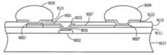
- a plurality of redistribution lines 1111 A-Cmay connect a respective plurality of solder bumps 1115 A-C to a single Vcc pad 1117 of the integrated circuit device, and each redistribution line 1111 A-C may include a respective pad portion 1111 A′, 1111 B′, and 1111 C′.
- the integrated circuit devicemay include a semiconductor substrate 1119 , a first insulating layer 1121 , and a second insulating layer 1123 .
- a conductive line (or trace) 905may be coupled to a circular conductive pad 903 .
- the conductive line 905may provide electrical interconnection between the conductive pad 903 and an input/output pad of an integrated circuit device, and a solder bump may be electrically coupled to the conductive pad 903 .
- FIGS. 1 A-C and 2 A-BParticular embodiments of the present invention including “D” shaped and crescent shaped vias are discussed above with respect to FIGS. 1 A-C and 2 A-B by way of example. Vias having other shapes and/or deviating from the particular shapes of FIGS. 1 A-C and 2 A-B may be provided according to other embodiments of the present invention. For example, sharp transitions of the perimeter of the via may be rounded either intentionally and/or as a result of processing tolerances.
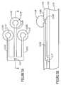
- a relatively short conductive line (or trace) 7001may be provided between input/output pad 7003 and primary solder bump 7005
- a relatively long conductive line (or trace) 7007may be provided between input/output pad 7003 and backup solder bump 7009 .
- the greater length of conductive line 7007 relative to conductive line 7001may provide a lesser resistance between input/output pad 7003 and primary solder bump 7005 than between input/output pad 7003 and secondary solder bump 7009 . Accordingly, current into and out of the input/output pad 7003 may flow primarily through conductive line 7001 and primary bump 7005 providing a path of least resistance. In the event of failure of a joint with the primary bump 7005 , current may then pass through conductive line 7007 and secondary bump 7009 .
- one or both of the via holes through the insulating layer 8115 exposing conductive pads 8001 ′ and/or 8007 ′may have a non-circular perimeter as discussed above with respect to FIGS. 1 A-C. More particularly, one or both of the via holes through the insulating layer 8115 exposing conductive pads 8001 ′ and/or 8007 ′ may have a “D” shaped and/or a crescent shaped perimeter as discussed above with respect to FIGS. 1 A-C.
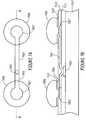
- a relatively thick conductive line (or trace) 9001may be provided between input/output pad 9003 and primary solder bump 9005
- a relatively thin conductive line (or trace) 9007may be provided between input/output pad 9003 and backup solder bump 9009 .
- the greater thickness of conductive line 9007 relative to conductive line 9001may provide a lesser resistance between input/output pad 9003 and primary solder bump 9005 than between input/output pad 9003 and secondary solder bump 9009 . Accordingly, current into and out of the input/output pad 9003 may flow primarily through conductive line 9001 and primary bump 9005 providing a path of least resistance.
- one or both of the via holes through the insulating layer 9115 exposing conductive pads 9001 ′ and/or 9007 ′may have a non-circular perimeter as discussed above with respect to FIGS. 1 A-C. More particularly, one or both of the via holes through the insulating layer 9115 exposing conductive pads 9001 ′ and/or 9007 ′ may have a “D” shaped and/or a crescent shaped perimeter as discussed above with respect to FIGS. 1 A-C.
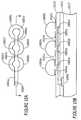
- the different segments 10001 a - c of the conductive linemay have different properties to provided further increases in resistance between solder bumps more distantly located from the input/output pad 10003 .
- a width of the segment 10001 amay be greater than a width of the segment 10001 b
- a width of the segment 10001 bmay be greater than a width of the segment 10001 c
- a thickness of the segment 10001 amay be greater than a thickness of the segment 10001 b
- a thickness of the segment 10001 bmay be greater than a thickness of the segment 10001 c .
- a length of the segment 10001 amay be less than a length of the segment 10001 b
- a length of the segment 10001 bmay be less than a length of the segment 10001 c.
Landscapes
- Engineering & Computer Science (AREA)
- Computer Hardware Design (AREA)
- Microelectronics & Electronic Packaging (AREA)
- Power Engineering (AREA)
- Internal Circuitry In Semiconductor Integrated Circuit Devices (AREA)
- Wire Bonding (AREA)
Abstract
Description
- The present application claims the benefit of priority as a Continuation-In-Part (CIP) application from U.S. Utility application Ser. No. 11/226,569 filed Sep. 14, 2005, which claims the benefit of priority as a Divisional application from U.S. Utility patent application Ser. No. 10/601,938 filed Jun. 23, 2003, which claims the benefit of priority from U.S. Provisional Application No. 60/391,511 filed Jun. 25, 2002. The present application also claims the benefit of priority from U.S. Provisional Application No. 60/626,802 filed Nov. 10, 2004. The disclosures of each of the above referenced utility and provisional applications are hereby incorporated herein in their entirety by reference.
- The present invention relates to the field of electronics, and more particularly to electronic structures including solder layers and related methods.
- Solder layers may be used to provide electrical and mechanical coupling between two electronic substrates, such as in flip-chip bonding. In particular, a solder layer may be provided on a conductive pad of an electronic substrate (such as an input/output pad of an integrated circuit substrate), and the solder layer can be used to bond the electronic substrate to a next level of packaging such as a printed circuit board, a ceramic substrate, and/or another integrated circuit device. Accordingly, the solder layer may provide an electrical interconnection between the electronic substrate and the next level of packaging.
- More particularly, a solder bump may be provided on a portion of a conductive pad exposed through a via in an insulating layer. In addition, a relatively thin underbump metallurgy (UBM) layer may promote adhesion, provide a plating electrode, and/or provide a routing conductor. An insulating layer on the electronic structure may include a via therein exposing a portion of the conductive pad on which the solder layer is provided. As current flowing in a conventional structure reaches an edge of a solder bump via, a lower resistance of the bump may cause most of the current to turn the corner at the via edge. A non-uniform current density may result, and a non-uniform current density may reduce reliability.
- More particularly, a relatively high current density at the via edge may accelerate local electromigration of the solder layer at the via edge. Solder, for example, may be particularly susceptible to electromigration because of its relatively low melting temperature. Diffusion of metal in the solder layer away from the via edge may result in formation of a void in the solder layer adjacent the via edge. The void may block current flow thus forcing the current to travel farther past the via edge before turning toward the solder. Accordingly, a void may grow laterally along an interface between the solder and the conductive pad.
- Solder layers may be relatively sensitive to electromigration as discussed, for example, by W. J. Choi et al. in “Electromigration Of Flip Chip Solder Bump On Cu/Ni(V)/Al Thin Film Under Bump Metallization” (Proceedings of the IEEE Electronic Components Technology Conference, 2002). The disclosure of the Choi et al. reference is hereby incorporated herein in its entirety by reference.
- According to some embodiments of the present invention, an integrated circuit device may include a substrate, a conductive pad on a surface of the substrate, and a conductive line on the surface of the substrate. The conductive line may be connected to the conductive pad, and the conductive line may be narrow relative to the conductive pad. An insulating layer may be provided on the substrate, on the conductive line, and on edge portions of the conductive pad, and the insulating layer may have a hole therein exposing a central portion of the conductive pad. In addition, a first segment of a perimeter of the hole may substantially define an arc of a circle around the central portion of the conductive pad, and a second segment of the perimeter of the hole may substantially deviate from the circle around the central portion of the conductive pad. Moreover, the second segment of the perimeter of the hole may be adjacent a connection between the conductive line and the conductive pad.
- A conductive bump may be provided on the central portion of the conductive pad and on portions of the insulating layer surrounding the hole so that the insulating layer is between the conductive bump and edge portions of the conductive pad. Moreover, the conductive bump may include a solder bump, and/or the conductive bump may have a substantially circular footprint on the insulating layer. In addition, an underbump metallurgy layer may be provided on the central portion of the conductive pad and on portions of the insulating layer surrounding the hole so that the under bump metallurgy layer is between the conductive bump and portions of the insulating layer surrounding the hole, and the underbump metallurgy layer and the conductive bump may comprise different materials.
- An input/output pad may be provided on the substrate, and the conductive line may provide electrical connection between the conductive pad and the input/output pad. In addition, a second conductive line may be connected to the input/output pad, and a second conductive pad may be connected to the second conductive line wherein the insulating layer has a second hole therein exposing a central portion of the second conductive pad. In addition, a first conductive bump may be provided on the central portion of the first conductive pad and on portions of the insulating layer surrounding the first hole, and a second conductive bump may be provided on the central portion of the second conductive pad and on portions of the insulating layer surrounding the second hole.
- According to some embodiments of the present invention, the second segment of the perimeter of the hole may substantially define a line, and a length of the second segment may be at least as great as a width of the conductive line. According to other embodiments of the present invention, the second segment of the perimeter of the hole may curve toward the center of the conductive pad.
- According to additional embodiments of the present invention, an integrated circuit device may include a substrate, a conductive pad on a surface of the substrate, and a conductive line on the surface of the substrate. The conductive line may be connected to the conductive pad, and the conductive line may be narrow relative to the conductive pad. An insulating layer may be provided on the substrate, on the conductive line, and on edge portions of the conductive pad, the insulating layer may have a hole therein exposing a central portion of the conductive pad, and at least a segment of a perimeter of the hole may be non-circular. In addition, a conductive bump may be provided on the central portion of the conductive pad and on portions of the insulating layer surrounding the hole so that the insulating layer is between the conductive bump and edge portions of the conductive pad and so that the conductive bump has a substantially circular footprint on the insulating layer.
- More particularly, the conductive bump may include a solder bump. In addition, an underbump metallurgy layer may be provided on the central portion of the conductive pad and on portions of the insulating layer surrounding the hole so that the under bump metallurgy layer is between the conductive bump and portions of the insulating layer surrounding the hole. Moreover, the underbump metallurgy layer and the conductive bump may include different materials.
- A first segment of a perimeter of the hole may substantially define an arc of a circle around the central portion of the conductive pad, and a second segment of the perimeter of the hole may substantially deviate from the circle around the central portion of the conductive pad. The second segment of the perimeter of the hole may be adjacent a connection between the conductive line and the conductive pad. According to some embodiments of the present invention, the second segment of the perimeter of the hole may substantially define a line, and a length of the second segment may be at least as great as a width of the conductive line. In other embodiments of the present invention, the second segment of the perimeter of the hole may curve toward the center of the conductive pad. Moreover, an input/output pad may be provided on the substrate wherein the conductive line provides electrical connection between the conductive pad and the input/output pad.
- In addition, the integrated circuit device may include a second conductive line connected to the input/output pad, and a second conductive pad connected to the second conductive line wherein the insulating layer has a second hole therein exposing a central portion of the second conductive pad. A first conductive bump may be provided on the central portion of the first conductive pad and on portions of the insulating layer surrounding the first hole, and a second conductive bump may be provided on the central portion of the second conductive pad and on portions of the insulating layer surrounding the second hole.
- According to additional embodiments of the present invention, an integrated circuit device may include a substrate, an input/output pad on the substrate, and first and second conductive lines on the substrate with both of the first and second lines being connected to the input/output pad. First and second conductive pads may be provided on the substrate with the first conductive pad being connected to the first conductive line and with the second conductive pad being connected to the second conductive line. An insulating layer may be provided on the first and second conductive lines and on edge portions of the first and second conductive pads, and the insulating layer may have first and second holes therein exposing central portions of the respective first and second conductive pads. In addition, a first conductive bump may be provided on the central portion of the first conductive bump and on portions of the insulating layer surrounding the first hole, and a second conductive bump may be provided on the central portion of the second conductive pad and on portions of the insulating layer surrounding the second hole.
- The first and second conductive bumps may include respective first and second solder bumps, and each of the first and second conductive bumps may have a substantially circular footprint on the insulating layer. In addition, a first underbump metallurgy layer may be provided on the central portion of the first conductive pad and on portions of the insulating layer surrounding the first hole so that the first under bump metallurgy layer is between the first conductive bump and portions of the insulating layer surrounding the first hole, and the first underbump metallurgy layer and the first conductive bump may include different materials. A second underbump metallurgy layer may be provided on the central portion of the second conductive pad and on portions of the insulating layer surrounding the second hole so that the second under bump metallurgy layer is between the second conductive bump and portions of the insulating layer surrounding the second hole, and the second underbump metallurgy layer and the second conductive bump may include different materials.
- The first conductive line may provide a first electrical resistance between the input/output pad and the first conductive pad, the second conductive line may provide a second electrical resistance between the input/output pad and the second conductive pad, and the first and second electrical resistances may be different. According to some embodiments of the present invention, the first conductive line may have a first length between the input/output pad and the first conductive pad, the second conductive line may have a second length between the input/output pad and the second conductive pad, and the first and second lengths may be different. According to some other embodiments of the present invention, the first conductive line may have a first width, the second conductive line may have a second width, and the first and second widths may be different. According to still other embodiments of the present invention, the first conductive line may have a first thickness, the second conductive line may have a second thickness, and the first and second thicknesses may be different. According to yet other embodiments of the present invention, the first conductive line may include a first material, the second conductive line may include a second material, and the first and second materials may be different.
- The input/output pad may be a ground pad providing a ground connection for the integrated circuit device, or the input/output pad may be a power pad providing a power connection for the integrated circuit device. The first conductive line may be narrow relative to the first conductive pad, a first segment of a perimeter of the first hole may substantially define an arc of a circle around the central portion of the first conductive pad, and a second segment of the perimeter of the first hole may substantially deviate from the circle around the central portion of the conductive pad. Moreover, the second segment of the perimeter of the first hole may be adjacent a connection between the conductive line and the conductive pad. Moreover, at least a segment of a perimeter of the first hole may be non-circular.
FIG. 1A is a top view illustrating a conductive line and pad according to embodiments of the present invention.- FIGS.1B-C are cross sectional views illustrating conductive lines and pads according to embodiments of the present invention.
FIG. 2A is a top view illustrating current concentrations on a conductive line and pad according to embodiments of the present invention.FIG. 2B is a mapping of greyscale shades fromFIG. 2A with respect to current densities.- FIGS.3A-B are cross sectional views illustrating power bumps according to embodiments of the present invention.
- FIGS.4A-B are cross sectional views illustrating ground bumps according to embodiments of the present invention.
- FIGS.5A-B are respective top and cross sectional views illustrating multiple bumps connected to an input/output pad according to some embodiments of the present invention.
- FIGS.6A-B are respective top and cross sectional views illustrating multiple bumps connected to an input/output pad according to some other embodiments of the present invention.
- FIGS.7A-B are respective top and cross sectional views illustrating multiple bumps connected to an input/output pad according to some additional embodiments of the present invention.
- FIGS.8A-B are respective top and cross sectional views illustrating multiple bumps connected to an input/output pad according to some more embodiments of the present invention.
- FIGS.9A-B are respective top and cross sectional views illustrating multiple bumps connected to an input/output pad according to still more embodiments of the present invention.
- FIGS.10A-B are respective top and cross sectional views illustrating multiple bumps connected to an input/output pad according to yet more embodiments of the present invention.
- The present invention now will be described more fully hereinafter with reference to the accompanying drawings, in which embodiments of the invention are shown. This invention may, however, be embodied in many different forms and should not be construed as limited to the embodiments set forth herein. Rather, these embodiments are provided so that this disclosure will be thorough and complete, and will fully convey the scope of the invention to those skilled in the art.
- In the drawings, the thickness of layers and regions are exaggerated for clarity. It will also be understood that when an element such as a layer, region or substrate is referred to as being on another element, it can be directly on the other element or intervening elements may also be present. In contrast, if an element such as a layer, region or substrate is referred to as being directly on another element, then no other intervening elements are present. Similarly, when an element such as a layer, region or substrate is referred to as being coupled or connected to/with another element, it can be directly coupled or connected to/with the other element or intervening elements may also be present. In contrast, if an element such as a layer, region or substrate is referred to as being directly coupled or connected to/with another element, then no other intervening elements are present. As used herein, the term “and/or” includes any and all combinations of one or more of the associated listed items. The symbol “/” is also used as a shorthand notation for “and/or”.
- Embodiments of the invention are described herein with reference to cross-section illustrations that are schematic illustrations of idealized embodiments (and intermediate structures) of the invention. As such, variations from the shapes of the illustrations as a result, for example, of manufacturing techniques and/or tolerances, are to be expected. Thus, embodiments of the invention should not be construed as limited to the particular shapes of regions illustrated herein but are to include deviations in shapes that result, for example, from manufacturing. For example, an implanted region illustrated as a rectangle will, typically, have rounded or curved features and/or a gradient of implant concentration at its edges rather than a binary change from implanted to non-implanted region. Likewise, a buried region formed by implantation may result in some implantation in the region between the buried region and the surface through which the implantation takes place. Moreover, a patterned feature (such as a perimeter of a hole) illustrated having sharp transitions may typically have a rounded or curved transition. Thus, the regions illustrated in the figures are schematic in nature and their shapes are not intended to illustrate the actual shape of a region of a device and are not intended to limit the scope of the invention.
- Furthermore, relative terms, such as beneath, upper, lower, top, and/or bottom may be used herein to describe one element's relationship to another element as illustrated in the figures. It will be understood that relative terms are intended to encompass different orientations of the device in addition to the orientation depicted in the figures. For example, if the device in one of the figures is turned over, elements described as below other elements would then be oriented above the other elements. The exemplary term below, can therefore, encompasses both an orientation of above and below.
- It will be understood that although the terms first and second are used herein to describe various regions, layers and/or sections, these regions, layers and/or sections should not be limited by these terms. These terms are only used to distinguish one region, layer or section from another region, layer or section. Thus, a first region, layer or section discussed below could be termed a second region, layer or section, and similarly, a second region, layer or section could be termed a first region, layer or section without departing from the teachings of the present invention. Like numbers refer to like elements throughout.
- The terminology used herein is for the purpose of describing particular embodiments only and is not intended to be limiting of the invention. As used herein, the singular forms “a”, “an” and “the” are intended to include the plural forms as well, unless the context clearly indicates otherwise. It will be further understood that the terms “comprises,” “comprising,” “includes”, and/or “including,” when used in this specification, specify the presence of stated features, integers, steps, operations, elements, and/or components, but do not preclude the presence or addition of one or more other features, integers, steps, operations, elements, components, and/or groups thereof.
- Unless otherwise defined, all terms (including technical and scientific terms) used herein have the same meaning as commonly understood by one of ordinary skill in the art to which this invention belongs. It will be further understood that terms, such as those defined in commonly used dictionaries, should be interpreted as having a meaning that is consistent with their meaning in the context of the relevant art and the present disclosure and will not be interpreted in an idealized or overly formal sense unless expressly so defined herein.
- Several approaches are discussed to reduce electromigration. According to embodiments of the present invention, effects of electromigration can be reduced by using more power or ground bumps depending on an expected operating temperature of a solder bump interconnection (such as a SnPb solder bump interconnection) because segregation of lead and tin may be a risk at the cathode below 100 degrees C. and at the anode above 100 degrees C. due to the relative diffusivities of the two components.
- More particularly, diffusivities of lead and tin in a lead-tin solder may vary over temperature, with lead diffusing faster than tin at temperatures greater than approximately 100 degrees C. and with tin diffusing faster than lead at temperatures less than approximately 100 degrees C. Moreover, a faster diffusing component of the solder metallurgy may tend to segregate toward a positive terminal (i.e., an anode) of the solder bump, and/or a slower diffusing component of the solder metallurgy may tend to segregate toward a negative terminal (i.e., a cathode) of the solder bump. An increased tin concentration may damage an under bump metallurgy layer between a lead-tin solder bump and a contact pad of an integrated circuit device.
- As shown in FIGS.3A-B, a power bump may be connected between a power supply conductor (anode) of a printed circuit board and a Vcc pad (cathode) of an integrated circuit device. As shown in
FIG. 3A , above approximately 100 degrees C., tin may segregate toward the Vcc pad of the integrated circuit device, and lead may segregate toward the power supply conductor of the printed circuit board. As shown inFIG. 3B , below approximately 100 degrees C., lead may segregate toward the Vcc pad of the integrated circuit device, and tin may segregate toward the power supply conductor of the printed circuit board. According to embodiments of the present invention, a plurality of power bumps may be provided for an integrated circuit device when operating conditions for the integrated circuit device are generally expected to exceed approximately 100 degrees C. For example, a plurality of redistribution lines may connect a respective plurality of solder bumps to a single power pad of the integrated circuit device. - If operating conditions for an integrated circuit device are generally expected to exceed approximately 100 degrees C., a number of power bumps provided for the integrated circuit device may exceed a number of ground bumps provided for the integrated circuit device. While particular embodiments of the present invention have been discussed with respect to binary solid solution solders such as lead-tin solders, other solid solution solders (including higher order solid solution solders) may be used. Moreover, binary and higher order intermetallic compound solders such as tin-silver and tin-silver-copper solders may also be used according to embodiments of the present invention.
- As shown in the top view of
FIG. 5A and in the corresponding cross sectional view ofFIG. 5B , for example, a plurality ofredistribution lines 1111A-C may connect a respective plurality of solder bumps1115A-C to asingle Vcc pad 1117 of the integrated circuit device, and eachredistribution line 1111A-C may include arespective pad portion 1111A′,1111B′, and1111C′. More particularly, the integrated circuit device may include asemiconductor substrate 1119, a first insulatinglayer 1121, and a second insulatinglayer 1123. The redistribution lines1111A-C may be provided between the first and second insulatinglayers layer 1123 may exposepad portions 1111A′,1111B′, and1111C′ of theredistribution lines pad portions 1111A′,1111B′, and1111C′ of the redistribution lines. The underbump metallurgy layer 1125B is shown in the cross sectional view ofFIG. 5B . - In addition or in an alternative, a plurality of solder bumps may be connected to a respective plurality of Vcc pads. By providing a plurality of power bumps, current can be distributed, and segregation can be reduced. Moreover, failure of a single power bump may not be catastrophic.
- While not shown in FIGS.5A-B, one or more of the via holes through the insulating
layer 1123 exposingconductive pads 1111A′,1111B′, and/or1111C′ may have a non-circular perimeter as discussed below with respect to FIGS.1A-C. More particularly, one or more of the via holes through the insulatinglayer 1123 exposing one or more ofconductive pads 1111A′,1111B′, and/or1111C′ may have a “D” shaped and/or a crescent shaped perimeter as discussed below with respect to FIGS.1A-C. - As shown in FIGS.4A-B, a ground bump may be connected between a ground conductor (cathode) of a printed circuit board and a ground pad (anode) of an integrated circuit device. As shown in
FIG. 4A , above approximately 100 degrees C., lead may segregate toward the ground pad of the integrated circuit device, and tin may segregate toward the ground conductor of the printed circuit board. As shown inFIG. 4B , below approximately 100 degrees C., tin may segregate toward the ground pad of the integrated circuit device, and lead may segregate toward the ground conductor of the printed circuit board. According to embodiments of the present invention, a plurality of ground bumps may be provided for an integrated circuit device when operating conditions for the integrated circuit device are generally expected not to exceed approximately 100 degrees C. For example, a plurality of redistribution lines may connect a respective plurality of solder bumps to a single ground pad of the integrated circuit device. - If operating conditions for an integrated circuit device are generally expected not to exceed approximately 100 degrees C., a number of ground bumps provided for the integrated circuit device may exceed a number of power bumps provided for the integrated circuit device. While particular embodiments of the present invention have been discussed with respect to binary solid solution solders such as lead-tin solders, other solid solution solders (including higher order solid solution solders) may be used. Moreover, binary and higher order intermetallic compound solders such as tin-silver and tin-silver-copper solders may also be used according to embodiments of the present invention.
- As shown in the top view of
FIG. 6A and in the corresponding cross sectional view ofFIG. 6B , for example, a plurality ofredistribution lines 2111A-C may connect a respective plurality of solder bumps2115A-C to asingle ground pad 2117 of the integrated circuit device, and eachredistribution line 2111A-C may include arespective pad portion 2111A′,2111B′, and2111C′. More particularly, the integrated circuit device may include asemiconductor substrate 2119, a first insulatinglayer 2121, and a second insulatinglayer 2123. The redistribution lines2111A-C may be provided between the first and second insulatinglayers layer 2123 may exposepad portions 2111A′,2111B′, and2111C′ of theredistribution lines pad portions 2111A′,2111B′, and2111C′ of the redistribution lines. The underbump metallurgy layer 2125B is shown in the cross sectional view ofFIG. 6B . - While not shown in FIGS.6A-B, one or more of the via holes through the insulating
layer 2123 exposingconductive pads 2111A′,2111B′, and/or2111C′ may have a non-circular perimeter as discussed below with respect to FIGS.1A-C. More particularly, one or more of the via holes through the insulatinglayer 2123 exposing one or more ofconductive pads 2111A′,2111B′, and/or2111C′ may have a “D” shaped and/or a crescent shaped perimeter as discussed below with respect to FIGS.1A-C. - In addition or in an alternative, a plurality of solder bumps may be connected to a respective plurality of ground pads. By providing a plurality of ground bumps, current can be distributed, and segregation can be reduced. Moreover, failure of a single ground bump may not be catastrophic.
- Benefits may also be provided according to embodiments of the present invention by connecting a plurality of solder bumps to input/output pads other than ground and/or Vcc pads. As discussed above with respect to ground and Vcc pads, current can be distributed and segregation can be reduced, and failure of a single bump may not be catastrophic. Provision of multiple bumps may be particularly, beneficial with input/output pads carrying currents sufficient to result in accumulation of vacancies at interfaces between a solder bump and its under bump metallurgy. For example, provision of multiple bumps may be beneficial where relatively large DC currents are provided through a pad (such as a ground and/or Vcc pad). Provision of multiple bumps may also be beneficial where intermittent unidirectional currents are provided through a pad (such as a pad providing a Pulse Width Modulation signal) and/or where bi-directional currents which are predominate in one direction are provided through a pad (such as a pad providing a Pulse-Reverse Plating signal). In addition, provision of multiple bumps may be beneficial wherein sufficiently high AC currents are provided through a pad such that vacancies may accumulate at a solder bump interface during half cycles of the signal.
- By providing a plurality of solder bumps connected to a same pad such as a ground pad, a Vcc pad, and/or an input/output pad, a device lifetime may be increased. More particularly, different resistances may be provided between the pad and each of the solder bumps connected to the pad so that, initially, current predominantly flows between the pad and a first solder bump connected through a path of least electrical resistance. Accordingly, vacancies (due to electromigration) may initially accumulate between the first solder bump and the respective under bump metallurgy layer, and vacancies may not substantially accumulate at a second solder bump connected through a path of higher resistance while the first solder bump is operational. The accumulation of vacancies at the first solder bump may eventually result in a void at the first solder bump and then failure of the first solder bump. Because significant current may not flow through the second solder bump until the first solder bump fails (due to the higher electrical resistance between the second solder bump and the pad), vacancies may not begin to significantly accumulate at the second solder bump until after failure of the first solder bump. An initiation of incubation of vacancies and/or voids in the second solder bump may thus be substantially delayed until after failure of the first solder bump. Stated in other words, initiation of a failure mechanism in the second solder bump may be substantially delayed until after failure of the first solder bump.
- According to additional embodiments of the present invention, effects of electromigration can be reduced by providing a ‘D’ shaped via with a flat of the D facing the conductive line or trace (i.e. facing the incoming/outgoing current flow). This structure may reduce current crowding at a short path to a nearest point of a conventional circular via. In an alternative, the via can be concave and/or crescent shaped in the direction of the conductive line or trace (i.e. in the direction of the incoming/outgoing current flow.
- As shown in the top view of
FIG. 1A , a conductive line (or trace)905 (such as a redistribution routing line) may be coupled to a circularconductive pad 903. Theconductive line 905, for example, may provide electrical interconnection between theconductive pad 903 and an input/output pad of an integrated circuit device, and a solder bump may be electrically coupled to theconductive pad 903. Moreover, theconductive line 905 andpad 903 may be covered by a subsequently formed insulating layer, and a viahole 918 may be formed in the insulating layer so that edge (or peripheral) portions903aof thepad 903 remain covered by the insulating layer and central (or interior) portions903bare exposed by the viahole 918. Stated in other words, central (or interior) portions903bof theconductive pad 903 may be free of the insulating layer. - As shown in
FIG. 1A , a perimeter of the viahole 918 may have a “D” shape as illustrated by thesegments linear segment 917′ of the perimeter of the “D” shaped viahole 918 may be adjacent and/or closest to the conductive line (or trace)905. In an alternative, the perimeter of the viahole 918 may have a crescent shape as illustrated by thesegments segment 917″ of the viahole 918 may be adjacent and/or closest to theconductive line 905. - According to some embodiments of the present invention, a
first segment 917 of the perimeter of the viahole 918 may substantially define an arc of a circle around central portions of theconductive pad 903. In addition, asecond segment 917′ or917″ of the perimeter of the viahole 918 may substantially deviate from the circle around the central portion of theconductive pad 903. Moreover, thesecond segment 917′ or917″ of the perimeter of the viahole 918 may be adjacent a connection between theconductive line 905 and theconductive pad 903. More particularly, the second segment of the perimeter of the viahole 918 may define a line as shown by thesegment 917′, and a length of thesecond segment 917′ may be at least as great as a width of the conductive line. In an alternative, thesecond segment 917″ of the perimeter of the viahole 918 may curve toward a center of theconductive pad 903. According to some other embodiments of the present invention, at least a segment of the perimeter of the via hole may be non-circular. - The cross sectional view of
FIG. 1B illustrates theconductive line 905 andpad 903 in an electronic device including asubstrate 901 and an insulatinglayer 907. The viahole 917 may expose a portion of theconductive pad 903B having a “D” shape and/or a crescent shape. Stated in other words, a perimeter of the viahole 918 may have a “D” shape and/or a crescent shape. - The cross sectional view of
FIG. 1C illustrates the structure ofFIG. 1B with the under bump metallurgy (UBM)layer 911 andsolder bump 920 formed thereon. As shown inFIG. 1C , portions of theUBM layer 911 and thesolder bump 920 may extend over portions of the insulatinglayer 907 outside the via hole. Accordingly, portions of theUBM layer 911 and thesolder bump 920 extending on the insulatinglayer 907 may define a circle even though the via hole is not circular. Accordingly, asolder bump 920 having a circular footprint may be provided even though a perimeter of the via hole through the insulatinglayer 907 has a “D” shape and/or a crescent shape. - Elements of structures illustrated in FIGS.1A-C may be formed as discussed, for example, in U.S. patent application Ser. No. 10/601,938 filed Jun. 23, 2003, the disclosure of which is hereby incorporated herein in its entirety by reference. For example, the
conductive line 905 andpad 903 may include a patterned layer(s) of a conductive material(s) such as copper, aluminum, nickel, titanium, and/or combinations and/or alloys thereof. TheUBM layer 911 may include one or more of an adhesion layer (such as a layer(s) of titanium, tungsten, chrome, and/or combinations and/or alloys thereof); a plating conduction layer (such as a layer of copper having a thickness in the range of approximately 0.1 to approximately 0.5 micrometers); a conductive shunt layer (such as a layer of copper having a thickness in the range of approximately 1.0 to approximately 5.0 micrometers); and/or a barrier layer (such as a layer(s) of nickel, platinum, palladium, and/or combinations and/or alloys thereof). Thesolder bump 920 may include lead-tin solder, but other solders may be used. - FIGS.2A-B illustrate current concentrations from a conductive line905 (for example, a redistribution line) to a
conductive pad 903 exposed through a crescent shaped viahole 918 with aconcave segment 917″ of the crescent toward the current carryingconductive line 905. As shown inFIG. 2A , a concentration of current entering/leaving the solder bump through theconductive pad 903 may be reduced. As shown inFIG. 2A , a greatest concentration of current may be provided through theconductive line 905, and least concentrations of current may be provided at portions of theconductive pad 903 opposite theconductive line 905 and at acentral portion 933 of the via hole. Greyscale shading between theconductive line 905 and theconcave segment 917″ of the crescent illustrates a spreading (reduced concentration) of current entering/leaving the solder bump relative to a pad with a via hole having a circular perimeter. - Particular embodiments of the present invention including “D” shaped and crescent shaped vias are discussed above with respect to FIGS.1A-C and2A-B by way of example. Vias having other shapes and/or deviating from the particular shapes of FIGS.1A-C and2A-B may be provided according to other embodiments of the present invention. For example, sharp transitions of the perimeter of the via may be rounded either intentionally and/or as a result of processing tolerances.
- According to additional embodiments of the present invention, increased solder bump life may be provided by reserving backup bumps that pass little current until a respective primary bump fails. Because nucleation of voids proceeds at a rate slower than void growth, relatively little nucleation may occur in a backup bump until the primary bump fails, and void nucleation in the backup bump may not substantially begin until after failure of the first bump when the backup bump begins carrying significant current. More particularly, separate redistribution lines may be provided from an integrated circuit contact pad to primary and backup solder bumps, and the redistribution line to the backup solder bump may provide a higher resistance than the redistribution line to the primary solder bump so that during normal operation, the backup solder bump carries significantly less current than the primary solder bump. For example, the redistribution line to the backup solder bump may be narrower, thinner, and/or longer than the redistribution line to the primary solder bump. Accordingly, the redistribution line to the backup solder bump may provide a resistance sufficiently greater than that of the redistribution line to the primary solder bump so that the primary solder bump carries significantly more current during normal operations. The resistance of the redistribution line to the backup solder bump, however, is sufficiently low so that performance of the integrated circuit device is not significantly diminished on failure of the primary solder bump. A failure mechanism resulting from void nucleation and growth in the backup solder bump may thus not substantially begin until after failure of the primary solder bump.
- While not shown in FIGS.1A-C and2A-B, the
conductive line 905 may be coupled to an input/output pad on thesubstrate 901. Theconductive line 905 may be coupled to an input/output pad as shown, for example, in FIGS.5A-B,6A-B,7A-B,8A-B,9A-B, and/or10A-B. Moreover, theconductive line 905 may be one of a plurality of conductive lines coupled to a same input/output pad so that there is a redundancy of electrical connection between a single input/output pad and a next level of packaging. - As shown in the top view of
FIG. 7A and the cross sectional view ofFIG. 7B , a relatively short conductive line (or trace)7001 may be provided between input/output pad 7003 andprimary solder bump 7005, and a relatively long conductive line (or trace)7007 may be provided between input/output pad 7003 andbackup solder bump 7009. The greater length ofconductive line 7007 relative toconductive line 7001 may provide a lesser resistance between input/output pad 7003 andprimary solder bump 7005 than between input/output pad 7003 andsecondary solder bump 7009. Accordingly, current into and out of the input/output pad 7003 may flow primarily throughconductive line 7001 andprimary bump 7005 providing a path of least resistance. In the event of failure of a joint with theprimary bump 7005, current may then pass throughconductive line 7007 andsecondary bump 7009. - As further shown in
FIG. 7B , theconductive lines layers output pad 7003 may be provided betweensemiconductor substrate 7117 and first insulatinglayer 7111. Moreover, via holes in the second insulatinglayer 7115 may exposeconductive pads 7001′ and7007′ respectively connected toconductive lines bump metallurgy layers solder bumps conductive pads 7001′ and7007′ ofconductive lines - While not shown in FIGS.7A-B, one or both of the via holes through the insulating
layer 7115 exposingconductive pads 7001′ and/or7007′ may have a non-circular perimeter as discussed above with respect to FIGS.1A-C. More particularly, one or both of the via holes through the insulatinglayer 7115 exposingconductive pads 7001′ and/or7007′ may have a “D” shaped and/or a crescent shaped perimeter as discussed above with respect to FIGS.1A-C. - As shown in the top view of
FIG. 8A and the cross sectional view ofFIG. 8B , a relatively wide conductive line (or trace)8001 may be provided between input/output pad 8003 andprimary solder bump 8005, and a relatively narrow conductive line (or trace)8007 may be provided between input/output pad 8003 andbackup solder bump 8009. The greater width ofconductive line 8007 relative toconductive line 8001 may provide a lesser resistance between input/output pad 8003 andprimary solder bump 8005 than between input/output pad 8003 andsecondary solder bump 8009. Accordingly, current into and out of the input/output pad 8003 may flow primarily throughconductive line 8001 andprimary bump 8005 providing a path of least resistance. In the event of failure of a joint with theprimary bump 8005, current may then pass throughconductive line 8007 andsecondary bump 8009. - As further shown in
FIG. 8B , theconductive lines layers output pad 8003 may be provided betweensemiconductor substrate 8117 and first insulatinglayer 8111. Moreover, via holes in the second insulatinglayer 8115 may exposeconductive pads 8001′ and8007′ respectively connected toconductive lines bump metallurgy layers solder bumps conductive pads 8001′ and8007′ ofconductive lines - While not shown in FIGS.8A-B, one or both of the via holes through the insulating
layer 8115 exposingconductive pads 8001′ and/or8007′ may have a non-circular perimeter as discussed above with respect to FIGS.1A-C. More particularly, one or both of the via holes through the insulatinglayer 8115 exposingconductive pads 8001′ and/or8007′ may have a “D” shaped and/or a crescent shaped perimeter as discussed above with respect to FIGS.1A-C. - As shown in the top view of
FIG. 9A and the cross sectional view ofFIG. 9B , a relatively thick conductive line (or trace)9001 may be provided between input/output pad 9003 andprimary solder bump 9005, and a relatively thin conductive line (or trace)9007 may be provided between input/output pad 9003 andbackup solder bump 9009. The greater thickness ofconductive line 9007 relative toconductive line 9001 may provide a lesser resistance between input/output pad 9003 andprimary solder bump 9005 than between input/output pad 9003 andsecondary solder bump 9009. Accordingly, current into and out of the input/output pad 9003 may flow primarily throughconductive line 9001 andprimary bump 9005 providing a path of least resistance. In the event of failure of a joint with theprimary bump 9005, current may then pass throughconductive line 9007 andsecondary bump 9009. The primary and backup conductive lines may include a common conductive layer(s)9031 which may be formed using a same deposition(s), and the primary conductive line may include an additional conductive layer(s)9033 not included in the backup conductive line. In an alternative, layers of the primary and backup conductive lines may be separately formed to have different thicknesses. In yet another alternative, the primary and backup conductive lines may include different conductive materials providing different resistances. - As further shown in
FIG. 9B , theconductive lines layers output pad 9003 may be provided betweensemiconductor substrate 9117 and first insulatinglayer 9111. Moreover, via holes in the second insulatinglayer 9115 may exposeconductive pads 9001′ and9007′ respectively connected toconductive lines bump metallurgy layers solder bumps conductive pads 9001′ and9007′ ofconductive lines - While not shown in FIGS.9A-B, one or both of the via holes through the insulating
layer 9115 exposingconductive pads 9001′ and/or9007′ may have a non-circular perimeter as discussed above with respect to FIGS.1A-C. More particularly, one or both of the via holes through the insulatinglayer 9115 exposingconductive pads 9001′ and/or9007′ may have a “D” shaped and/or a crescent shaped perimeter as discussed above with respect to FIGS.1A-C. - As shown in the top view of
FIG. 10A and the cross sectional view ofFIG. 10B , a plurality of solder bumps10005a-cmay be provided along a same conductive line (or trace) including segments10001a-cconnected to input/output pad 10003. The lesser distance between thesolder bump 10005aand the input/output pad 10003 relative to the solder bumps10005b-cmay provide a lesser resistance between input/output pad 10003 andprimary solder bump 10005athan between input/output pad 10003 and secondary solder bumps10005bor10005c. Accordingly, current into and out of the input/output pad 10003 may flow primarily throughprimary bump 10005aproviding a path of least resistance. In the event of failure of a joint with theprimary bump 10005a, current may then pass through conductive line segments10001a-bandsecondary bump 10005b. In the event of failure of a joint with theprimary bump 10005aand the firstsecondary bump 10005b, current may then pass through conductive line segments10001a-cand secondsecondary bump 10005c. - As further shown in
FIG. 10B , the conductive line segments10001a-cmay be provided between first and second insulatinglayers output pad 10003 may be provided betweensemiconductor substrate 10117 and first insulatinglayer 10111. Moreover, via holes in the second insulatinglayer 10115 may exposeconductive pads 10001a′,10001b′, and10001c′ respectively connected to the conductive line including segments10001a-c, and under bump metallurgy layers10121a-cmay be provided between solder bumps10005a-cand the respectiveconductive pads 10001a′-c′. - Moreover, the different segments10001a-cof the conductive line may have different properties to provided further increases in resistance between solder bumps more distantly located from the input/
output pad 10003. For example, a width of thesegment 10001amay be greater than a width of thesegment 10001b, and/or a width of thesegment 10001bmay be greater than a width of thesegment 10001c. In addition or in an alternative, a thickness of thesegment 10001amay be greater than a thickness of thesegment 10001b, and/or a thickness of thesegment 10001bmay be greater than a thickness of thesegment 10001c. Moreover, a length of thesegment 10001amay be less than a length of thesegment 10001b, and/or a length of thesegment 10001bmay be less than a length of thesegment 10001c. - While not shown in FIGS.10A-B, one or both of the via holes through the insulating
layer 10115 exposingconductive pads 10001a′-c′ may have a non-circular perimeter as discussed above with respect to FIGS.1A-C. More particularly, one or both of the via holes through the insulatinglayer 10115 exposingconductive pads 10001a′-c′ may have a “D” shaped and/or a crescent shaped perimeter as discussed above with respect to FIGS.1A-C. - As used herein, the term under bump metallurgy layer refers to one or more conductive layers provided between a solder bump and a substrate. An under bump metallurgy layer may include an adhesion layer (such as a layer of titanium, tungsten, chrome, and/or combinations thereof), a conduction layer (such as a layer of copper), and/or a barrier layer (such as a layer of nickel, platinum, palladium, and/or combinations thereof). A solder bump may be a bump of one or more different solder materials. For example, a solder bump may include one or more of a single element, binary, ternary, and/or higher order solder; such as a lead-tin solder, a lead-bismuth solder, a lead-indium solder, a lead free solder, a tin-silver solder, a tin-silver-copper solder, an indium-tin solder, an indium-gallium solder, a gallium solder, an indium-bismuth solder, a tin-bismuth solder, an indium-cadmium solder, bismuth-cadmium solder, tin-cadmium, etc. Accordingly, an under bump metallurgy layer may provide a surface that is wettable to a solder bump wherein the solder wettable surface of the under bump metallurgy layer and the solder bump comprise different materials.
- While the present invention has been particularly shown and described with reference to embodiments thereof, it will be understood by those skilled in the art that various changes in form and details may be made therein without departing from the spirit and scope of the invention as defined by the appended claims and their equivalents.
Claims (34)
Priority Applications (1)
| Application Number | Priority Date | Filing Date | Title |
|---|---|---|---|
| US11/270,366US7531898B2 (en) | 2002-06-25 | 2005-11-09 | Non-Circular via holes for bumping pads and related structures |
Applications Claiming Priority (5)
| Application Number | Priority Date | Filing Date | Title |
|---|---|---|---|
| US39151102P | 2002-06-25 | 2002-06-25 | |
| US10/601,938US6960828B2 (en) | 2002-06-25 | 2003-06-23 | Electronic structures including conductive shunt layers |
| US62680204P | 2004-11-10 | 2004-11-10 | |
| US11/226,569US7297631B2 (en) | 2002-06-25 | 2005-09-14 | Methods of forming electronic structures including conductive shunt layers and related structures |
| US11/270,366US7531898B2 (en) | 2002-06-25 | 2005-11-09 | Non-Circular via holes for bumping pads and related structures |
Related Parent Applications (1)
| Application Number | Title | Priority Date | Filing Date |
|---|---|---|---|
| US11/226,569Continuation-In-PartUS7297631B2 (en) | 2002-06-25 | 2005-09-14 | Methods of forming electronic structures including conductive shunt layers and related structures |
Publications (2)
| Publication Number | Publication Date |
|---|---|
| US20060076679A1true US20060076679A1 (en) | 2006-04-13 |
| US7531898B2 US7531898B2 (en) | 2009-05-12 |
Family
ID=36144447
Family Applications (1)
| Application Number | Title | Priority Date | Filing Date |
|---|---|---|---|
| US11/270,366Expired - Fee RelatedUS7531898B2 (en) | 2002-06-25 | 2005-11-09 | Non-Circular via holes for bumping pads and related structures |
Country Status (1)
| Country | Link |
|---|---|
| US (1) | US7531898B2 (en) |
Cited By (23)
| Publication number | Priority date | Publication date | Assignee | Title |
|---|---|---|---|---|
| US20070172981A1 (en)* | 2006-01-20 | 2007-07-26 | Meng-Jen Wang | Method for making flip chip on leadframe package |
| US20070228561A1 (en)* | 2006-03-31 | 2007-10-04 | Fujitsu Limited | Semiconductor device and manufacturing method thereof |
| KR100787892B1 (en) | 2006-10-31 | 2007-12-27 | 삼성전자주식회사 | Semiconductor package and manufacturing method thereof |
| WO2008059433A1 (en)* | 2006-11-13 | 2008-05-22 | Nxp B.V. | Bond pad structure and method for producing same |
| US20090016036A1 (en)* | 2007-07-13 | 2009-01-15 | Wong Shaw Fong | Conductor reinforcement for circuit boards |
| US20090289362A1 (en)* | 2008-05-21 | 2009-11-26 | Texas Instruments Incorporated | Low Inductance Ball Grid Array Device Having Chip Bumps on Substrate Vias |
| US20100155941A1 (en)* | 2007-07-25 | 2010-06-24 | Fujitsu Microelectronics Limited | Semiconductor device |
| US20110204511A1 (en)* | 2007-11-30 | 2011-08-25 | Texas Instruments Incorporated | System and Method for Improving Reliability of Integrated Circuit Packages |
| US20110233766A1 (en)* | 2010-03-25 | 2011-09-29 | Stats Chippac, Ltd. | Semiconductor Device and Method of Forming a Dual UBM Structure for Lead Free Bump Connections |
| US20110283034A1 (en)* | 2010-05-12 | 2011-11-17 | Samsung Electronics Co., Ltd. | Semiconductor chip, and semiconductor package and system each including the semiconductor chip |
| US20120126420A1 (en)* | 2010-11-19 | 2012-05-24 | Advanced Semiconductor Engineering, Inc. | Semiconductor device having conductive vias and semiconductor package having semiconductor device |
| US8298929B2 (en) | 2010-12-03 | 2012-10-30 | International Business Machines Corporation | Offset solder vias, methods of manufacturing and design structures |
| US20130113096A1 (en)* | 2010-07-09 | 2013-05-09 | Rohm Co., Ltd. | Semiconductor device |
| CN103367315A (en)* | 2013-07-08 | 2013-10-23 | 日月光半导体制造股份有限公司 | Wafer Level Package Construction |
| US8836835B2 (en) | 2010-10-04 | 2014-09-16 | International Business Machines Corporation | Pixel sensor cell with hold node for leakage cancellation and methods of manufacture and design structure |
| US20150123267A1 (en)* | 2013-11-06 | 2015-05-07 | Taiwan Semiconductor Manufacturing Company Ltd. | Packaged semiconductor device |
| US9123543B1 (en)* | 2008-05-07 | 2015-09-01 | Amkor Technology, Inc. | Semiconductor device and manufacturing method thereof |
| CN104916617A (en)* | 2014-03-13 | 2015-09-16 | 台湾积体电路制造股份有限公司 | Semiconductor device structure and manufacturing method |
| US20190189592A1 (en)* | 2017-12-20 | 2019-06-20 | Samsung Electronics Co., Ltd. | Semiconductor package and manufacturing method thereof |
| US20220384313A1 (en)* | 2020-07-17 | 2022-12-01 | Taiwan Semiconductor Manufacturing Co., Ltd. | Stacking Via Structures for Stress Reduction |
| US11749644B2 (en) | 2020-04-27 | 2023-09-05 | Taiwan Semiconductor Manufacturing Co., Ltd. | Semiconductor device with curved conductive lines and method of forming the same |
| US12094828B2 (en) | 2020-07-17 | 2024-09-17 | Taiwan Semiconductor Manufacturing Co., Ltd. | Eccentric via structures for stress reduction |
| US12148684B2 (en) | 2020-07-31 | 2024-11-19 | Taiwan Semiconductor Manufacturing Co., Ltd. | Package structure and method |
Families Citing this family (6)
| Publication number | Priority date | Publication date | Assignee | Title |
|---|---|---|---|---|
| TWI232072B (en)* | 2004-04-05 | 2005-05-01 | Wistron Corp | Method and structure for printed circuit board assembly and jig for assembling structure |
| US7547969B2 (en) | 2004-10-29 | 2009-06-16 | Megica Corporation | Semiconductor chip with passivation layer comprising metal interconnect and contact pads |
| US7397121B2 (en)* | 2005-10-28 | 2008-07-08 | Megica Corporation | Semiconductor chip with post-passivation scheme formed over passivation layer |
| KR20120039460A (en)* | 2010-10-15 | 2012-04-25 | 삼성전자주식회사 | Semiconductor package |
| KR101185859B1 (en) | 2010-10-19 | 2012-09-25 | 에스케이하이닉스 주식회사 | Bump for semiconductor package, semiconductor package and stacked semiconductor package having the bump |
| US12021048B2 (en)* | 2021-08-30 | 2024-06-25 | Taiwan Semiconductor Manufacturing Company, Ltd. | Semiconductor device |
Citations (96)
| Publication number | Priority date | Publication date | Assignee | Title |
|---|---|---|---|---|
| US162257A (en)* | 1875-04-20 | Improvement in cider-presses | ||
| US3244947A (en)* | 1962-06-15 | 1966-04-05 | Slater Electric Inc | Semi-conductor diode and manufacture thereof |
| US3259814A (en)* | 1955-05-20 | 1966-07-05 | Rca Corp | Power semiconductor assembly including heat dispersing means |
| US3316465A (en)* | 1961-03-29 | 1967-04-25 | Siemens Ag | Multi-layer junction semiconductor devices such as controlled rectifiers and transistors, containing electro-positive protective coating |
| US3489965A (en)* | 1967-04-04 | 1970-01-13 | Marconi Co Ltd | Insulated gate field effect transistors |
| US3501681A (en)* | 1966-07-19 | 1970-03-17 | Union Carbide Corp | Face bonding of semiconductor devices |
| US3586255A (en)* | 1967-10-27 | 1971-06-22 | Carpano & Pons | Spinning reel with winding drum brake |
| US3663184A (en)* | 1970-01-23 | 1972-05-16 | Fairchild Camera Instr Co | Solder bump metallization system using a titanium-nickel barrier layer |
| US3871014A (en)* | 1969-08-14 | 1975-03-11 | Ibm | Flip chip module with non-uniform solder wettable areas on the substrate |
| US3871015A (en)* | 1969-08-14 | 1975-03-11 | Ibm | Flip chip module with non-uniform connector joints |
| US3942187A (en)* | 1969-01-02 | 1976-03-02 | U.S. Philips Corporation | Semiconductor device with multi-layered metal interconnections |
| US3959577A (en)* | 1974-06-10 | 1976-05-25 | Westinghouse Electric Corporation | Hermetic seals for insulating-casing structures |
| US4074342A (en)* | 1974-12-20 | 1978-02-14 | International Business Machines Corporation | Electrical package for lsi devices and assembly process therefor |
| US4244002A (en)* | 1977-10-19 | 1981-01-06 | Nippon Electric Co., Ltd. | Semiconductor device having bump terminal electrodes |
| US4257905A (en)* | 1977-09-06 | 1981-03-24 | The United States Of America As Represented By The United States Department Of Energy | Gaseous insulators for high voltage electrical equipment |
| US4266282A (en)* | 1979-03-12 | 1981-05-05 | International Business Machines Corporation | Vertical semiconductor integrated circuit chip packaging |
| US4273859A (en)* | 1979-12-31 | 1981-06-16 | Honeywell Information Systems Inc. | Method of forming solder bump terminals on semiconductor elements |
| US4382517A (en)* | 1981-02-20 | 1983-05-10 | Metropolitan Wire Corporation | Panels for holding printed circuit boards |
| US4449580A (en)* | 1981-06-30 | 1984-05-22 | International Business Machines Corporation | Vertical wall elevated pressure heat dissipation system |
| US4505029A (en)* | 1981-03-23 | 1985-03-19 | General Electric Company | Semiconductor device with built-up low resistance contact |
| US4511873A (en)* | 1982-07-19 | 1985-04-16 | Bbc Brown, Boveri & Company, Limited | Current transformer insulated by pressurized gas |
| US4532576A (en)* | 1983-08-29 | 1985-07-30 | Gte Automatic Electric Incorporated | Printed wiring board file and method of utilizing the same |
| US4563697A (en)* | 1982-02-25 | 1986-01-07 | Fuji Electric Company, Ltd. | Semiconductor pressure sensor |
| US4565901A (en)* | 1983-06-14 | 1986-01-21 | Mitsubishi Denki Kabushiki Kaisha | Gas-insulated electric device |
| US4657146A (en)* | 1985-11-06 | 1987-04-14 | Richard Walters | Adjustable printed circuit board rack for supporting printed circuit boards in a horizontal or a vertical position |
| US4661375A (en)* | 1985-04-22 | 1987-04-28 | At&T Technologies, Inc. | Method for increasing the height of solder bumps |
| US4673772A (en)* | 1984-10-05 | 1987-06-16 | Hitachi, Ltd. | Electronic circuit device and method of producing the same |
| US4733813A (en)* | 1985-10-01 | 1988-03-29 | Bull S.A. | Method and apparatus for soldering elements on the corresponding pads of a wafer, in particular a wafer having high-density integrated circuits |
| US4752027A (en)* | 1987-02-20 | 1988-06-21 | Hewlett-Packard Company | Method and apparatus for solder bumping of printed circuit boards |
| US4817850A (en)* | 1988-03-28 | 1989-04-04 | Hughes Aircraft Company | Repairable flip-chip bumping |
| US4830264A (en)* | 1986-10-08 | 1989-05-16 | International Business Machines Corporation | Method of forming solder terminals for a pinless ceramic module |
| US4840302A (en)* | 1988-04-15 | 1989-06-20 | International Business Machines Corporation | Chromium-titanium alloy |
| US4893403A (en)* | 1988-04-15 | 1990-01-16 | Hewlett-Packard Company | Chip alignment method |
| US4897508A (en)* | 1988-02-10 | 1990-01-30 | Olin Corporation | Metal electronic package |
| US4897918A (en)* | 1985-07-16 | 1990-02-06 | Nippon Telegraph And Telephone | Method of manufacturing an interboard connection terminal |
| US4927505A (en)* | 1988-07-05 | 1990-05-22 | Motorola Inc. | Metallization scheme providing adhesion and barrier properties |
| US4931410A (en)* | 1987-08-25 | 1990-06-05 | Hitachi, Ltd. | Process for producing semiconductor integrated circuit device having copper interconnections and/or wirings, and device produced |
| US4940181A (en)* | 1989-04-06 | 1990-07-10 | Motorola, Inc. | Pad grid array for receiving a solder bumped chip carrier |
| US5019943A (en)* | 1990-02-14 | 1991-05-28 | Unisys Corporation | High density chip stack having a zigzag-shaped face which accommodates connections between chips |
| US5022580A (en)* | 1988-03-16 | 1991-06-11 | Plessey Overseas Limited | Vernier structure for flip chip bonded devices |
| US5024372A (en)* | 1989-01-03 | 1991-06-18 | Motorola, Inc. | Method of making high density solder bumps and a substrate socket for high density solder bumps |
| US5113314A (en)* | 1991-01-24 | 1992-05-12 | Hewlett-Packard Company | High-speed, high-density chip mounting |
| US5130275A (en)* | 1990-07-02 | 1992-07-14 | Digital Equipment Corp. | Post fabrication processing of semiconductor chips |
| US5130779A (en)* | 1990-06-19 | 1992-07-14 | International Business Machines Corporation | Solder mass having conductive encapsulating arrangement |
| US5194137A (en)* | 1991-08-05 | 1993-03-16 | Motorola Inc. | Solder plate reflow method for forming solder-bumped terminals |
| US5211807A (en)* | 1991-07-02 | 1993-05-18 | Microelectronics Computer & Technology | Titanium-tungsten etching solutions |
| US5216280A (en)* | 1989-12-02 | 1993-06-01 | Kabushiki Kaisha Toshiba | Semiconductor integrated circuit device having pads at periphery of semiconductor chip |
| US5227664A (en)* | 1988-02-26 | 1993-07-13 | Hitachi, Ltd. | Semiconductor device having particular mounting arrangement |
| US5289925A (en)* | 1992-03-16 | 1994-03-01 | Martin Newmark | Organizational display for compact disc jewel boxes |
| US5293006A (en)* | 1991-09-13 | 1994-03-08 | Mcnc | Solder bump including circular lip |
| US5325265A (en)* | 1988-11-10 | 1994-06-28 | Mcnc | High performance integrated circuit chip package |
| US5327013A (en)* | 1992-04-30 | 1994-07-05 | Motorola, Inc. | Solder bumping of integrated circuit die |
| US5381946A (en)* | 1992-03-04 | 1995-01-17 | Mcnc | Method of forming differing volume solder bumps |
| US5391514A (en)* | 1994-04-19 | 1995-02-21 | International Business Machines Corporation | Low temperature ternary C4 flip chip bonding method |
| US5406701A (en)* | 1992-10-02 | 1995-04-18 | Irvine Sensors Corporation | Fabrication of dense parallel solder bump connections |
| US5409862A (en)* | 1992-03-24 | 1995-04-25 | Kabushiki Kaisha Toshiba | Method for making aluminum single crystal interconnections on insulators |
| US5424920A (en)* | 1992-05-15 | 1995-06-13 | Irvine Sensors Corporation | Non-conductive end layer for integrated stack of IC chips |
| US5492235A (en)* | 1995-12-18 | 1996-02-20 | Intel Corporation | Process for single mask C4 solder bump fabrication |
| US5609287A (en)* | 1991-10-04 | 1997-03-11 | Mitsubishi Denki Kabushiki Kaisha | Solder material, junctioning method, junction material, and semiconductor device |
| US5616962A (en)* | 1992-01-24 | 1997-04-01 | Kabushiki Kaisha Toshiba | Semiconductor integrated circuit devices having particular terminal geometry |
| US5627396A (en)* | 1993-02-01 | 1997-05-06 | Brooktree Corporation | Micromachined relay and method of forming the relay |
| US5634268A (en)* | 1995-06-07 | 1997-06-03 | International Business Machines Corporation | Method for making direct chip attach circuit card |
| US5736456A (en)* | 1996-03-07 | 1998-04-07 | Micron Technology, Inc. | Method of forming conductive bumps on die for flip chip applications |
| US5739053A (en)* | 1992-10-27 | 1998-04-14 | Matsushita Electric Industrial Co., Ltd. | Process for bonding a semiconductor to a circuit substrate including a solder bump transferring step |
| US5744382A (en)* | 1992-05-13 | 1998-04-28 | Matsushita Electric Industrial Co., Ltd. | Method of packaging electronic chip component and method of bonding of electrode thereof |
| US5751556A (en)* | 1996-03-29 | 1998-05-12 | Intel Corporation | Method and apparatus for reducing warpage of an assembly substrate |
| US5759437A (en)* | 1996-10-31 | 1998-06-02 | International Business Machines Corporation | Etching of Ti-W for C4 rework |
| US5773359A (en)* | 1995-12-26 | 1998-06-30 | Motorola, Inc. | Interconnect system and method of fabrication |
| US5859470A (en)* | 1992-11-12 | 1999-01-12 | International Business Machines Corporation | Interconnection of a carrier substrate and a semiconductor device |
| US5886393A (en)* | 1997-11-07 | 1999-03-23 | National Semiconductor Corporation | Bonding wire inductor for use in an integrated circuit package and method |
| US5891756A (en)* | 1997-06-27 | 1999-04-06 | Delco Electronics Corporation | Process for converting a wire bond pad to a flip chip solder bump pad and pad formed thereby |
| US5892179A (en)* | 1995-04-05 | 1999-04-06 | Mcnc | Solder bumps and structures for integrated redistribution routing conductors |
| US5898574A (en)* | 1997-09-02 | 1999-04-27 | Tan; Wiling | Self aligning electrical component |
| US5902686A (en)* | 1996-11-21 | 1999-05-11 | Mcnc | Methods for forming an intermetallic region between a solder bump and an under bump metallurgy layer and related structures |
| US5906312A (en)* | 1994-12-02 | 1999-05-25 | Franunhofer-Gesellschaft Zur Foerde-Rung Der Angwandten Forschung E.V. | Solder bump for flip chip assembly and method of its fabrication |
| US6015505A (en)* | 1997-10-30 | 2000-01-18 | International Business Machines Corporation | Process improvements for titanium-tungsten etching in the presence of electroplated C4's |
| US6027957A (en)* | 1996-06-27 | 2000-02-22 | University Of Maryland | Controlled solder interdiffusion for high power semiconductor laser diode die bonding |
| US6169325B1 (en)* | 1997-12-17 | 2001-01-02 | Hitachi, Ltd. | Semiconductor device |
| US6208018B1 (en)* | 1997-05-29 | 2001-03-27 | Micron Technology, Inc. | Piggyback multiple dice assembly |
| US6221682B1 (en)* | 1999-05-28 | 2001-04-24 | Lockheed Martin Corporation | Method and apparatus for evaluating a known good die using both wire bond and flip-chip interconnects |
| US6222279B1 (en)* | 1995-03-20 | 2001-04-24 | Mcnc | Solder bump fabrication methods and structures including a titanium barrier layer |
| US6224690B1 (en)* | 1995-12-22 | 2001-05-01 | International Business Machines Corporation | Flip-Chip interconnections using lead-free solders |
| US6231743B1 (en)* | 2000-01-03 | 2001-05-15 | Motorola, Inc. | Method for forming a semiconductor device |
| US6238951B1 (en)* | 1993-05-28 | 2001-05-29 | Commissariat A L'energie Atomique | Process for producing a sealing and mechanical strength ring between a substrate and a chip hybridized by bumps on the substrate |
| US6335104B1 (en)* | 2000-02-22 | 2002-01-01 | International Business Machines Corporation | Method for preparing a conductive pad for electrical connection and conductive pad formed |
| US20020000665A1 (en)* | 1999-04-05 | 2002-01-03 | Alexander L. Barr | Semiconductor device conductive bump and interconnect barrier |
| US6346469B1 (en)* | 2000-01-03 | 2002-02-12 | Motorola, Inc. | Semiconductor device and a process for forming the semiconductor device |
| US6388203B1 (en)* | 1995-04-04 | 2002-05-14 | Unitive International Limited | Controlled-shaped solder reservoirs for increasing the volume of solder bumps, and structures formed thereby |
| US20020056742A1 (en)* | 2000-11-10 | 2002-05-16 | Rinne Glenn A. | Methods and systems for attaching substrates to one another using solder structures having portions with different melting points |
| US20020079576A1 (en)* | 2000-06-30 | 2002-06-27 | Krishna Seshan | Ball limiting metallurgy for input/outputs and methods of fabrication |
| US20030027379A1 (en)* | 2001-08-06 | 2003-02-06 | Hermen Liu | Laser repair operation |
| US20030060040A1 (en)* | 1998-07-31 | 2003-03-27 | Industrial Technology Research Institute | Method of electroless plating copper on nitride barrier |
| US20030107137A1 (en)* | 2001-09-24 | 2003-06-12 | Stierman Roger J. | Micromechanical device contact terminals free of particle generation |
| US20040053483A1 (en)* | 2002-06-25 | 2004-03-18 | Nair Krishna K. | Methods of forming electronic structures including conductive shunt layers and related structures |
| US20050012222A1 (en)* | 2003-07-15 | 2005-01-20 | Min-Lung Huang | [chip structure] |
| US6853076B2 (en)* | 2001-09-21 | 2005-02-08 | Intel Corporation | Copper-containing C4 ball-limiting metallurgy stack for enhanced reliability of packaged structures and method of making same |
Family Cites Families (133)
| Publication number | Priority date | Publication date | Assignee | Title |
|---|---|---|---|---|
| US3105869A (en) | 1962-03-23 | 1963-10-01 | Hughes Aircraft Co | Electrical connection of microminiature circuit wafers |
| US3274458A (en) | 1964-04-02 | 1966-09-20 | Int Rectifier Corp | Extremely high voltage silicon device |
| US3458925A (en) | 1966-01-20 | 1969-08-05 | Ibm | Method of forming solder mounds on substrates |
| US3461357A (en) | 1967-09-15 | 1969-08-12 | Ibm | Multilevel terminal metallurgy for semiconductor devices |
| GB1288564A (en) | 1969-01-24 | 1972-09-13 | ||
| US3625837A (en) | 1969-09-18 | 1971-12-07 | Singer Co | Electroplating solder-bump connectors on microcircuits |
| DE2044494B2 (en) | 1970-09-08 | 1972-01-13 | Siemens AG, 1000 Berlin u 8000 München | CONNECTING AREAS FOR SOLDERING SEMI-CONDUCTOR COMPONENTS IN FLIP CHIP TECHNOLOGY |
| US3760238A (en) | 1972-02-28 | 1973-09-18 | Microsystems Int Ltd | Fabrication of beam leads |
| JPS49135749U (en) | 1973-03-24 | 1974-11-21 | ||
| US4113578A (en) | 1973-05-31 | 1978-09-12 | Honeywell Inc. | Microcircuit device metallization |
| US3839727A (en) | 1973-06-25 | 1974-10-01 | Ibm | Semiconductor chip to substrate solder bond using a locally dispersed, ternary intermetallic compound |
| US3897871A (en) | 1973-07-26 | 1975-08-05 | Lilly Co Eli | Print album storage case insert |
| US4113587A (en) | 1974-08-05 | 1978-09-12 | Agency Of Industrial Science And Technology | Method for electrochemical machining |
| US3986255A (en) | 1974-11-29 | 1976-10-19 | Itek Corporation | Process for electrically interconnecting chips with substrates employing gold alloy bumps and magnetic materials therein |
| US3993123A (en) | 1975-10-28 | 1976-11-23 | International Business Machines Corporation | Gas encapsulated cooling module |
| JPS5450269U (en) | 1977-09-14 | 1979-04-07 | ||
| US4168480A (en) | 1978-02-13 | 1979-09-18 | Torr Laboratories, Inc. | Relay assembly |
| JPS54128669U (en) | 1978-02-27 | 1979-09-07 | ||
| JPS6222978Y2 (en) | 1979-01-31 | 1987-06-11 | ||
| JPS5678356U (en) | 1979-11-12 | 1981-06-25 | ||
| JPS5773952U (en) | 1980-09-11 | 1982-05-07 | ||
| US4473263A (en) | 1981-01-21 | 1984-09-25 | Sunstein Drew E | Circuit board mounting device and associated components |
| JPS57197838A (en) | 1981-05-29 | 1982-12-04 | Oki Electric Ind Co Ltd | Semiconductor flip chip element |
| JPS59154041U (en) | 1983-03-31 | 1984-10-16 | 九州積水工業株式会社 | Nori net drying frame |
| US4545610A (en) | 1983-11-25 | 1985-10-08 | International Business Machines Corporation | Method for forming elongated solder connections between a semiconductor device and a supporting substrate |
| JPH0766207B2 (en) | 1986-04-07 | 1995-07-19 | キヤノン株式会社 | Image recorder |
| US4878611A (en) | 1986-05-30 | 1989-11-07 | American Telephone And Telegraph Company, At&T Bell Laboratories | Process for controlling solder joint geometry when surface mounting a leadless integrated circuit package on a substrate |
| US4763829A (en) | 1986-06-04 | 1988-08-16 | American Telephone And Telegraph Company, At&T Bell Laboratories | Soldering of electronic components |
| GB2194387A (en) | 1986-08-20 | 1988-03-02 | Plessey Co Plc | Bonding integrated circuit devices |
| JPS6399558U (en) | 1986-12-18 | 1988-06-28 | ||
| JPH0793304B2 (en) | 1987-03-11 | 1995-10-09 | 富士通株式会社 | Method of forming bump electrode |
| JPS6461934A (en) | 1987-09-02 | 1989-03-08 | Nippon Denso Co | Semiconductor device and manufacture thereof |
| JPH0194696A (en) | 1987-10-06 | 1989-04-13 | Ibiden Co Ltd | Printed wiring board |
| US4855809A (en) | 1987-11-24 | 1989-08-08 | Texas Instruments Incorporated | Orthogonal chip mount system module and method |
| JPH01214141A (en) | 1988-02-23 | 1989-08-28 | Nec Corp | Flip-chip type semiconductor device |
| US4950623A (en) | 1988-08-02 | 1990-08-21 | Microelectronics Center Of North Carolina | Method of building solder bumps |
| US4861425A (en) | 1988-08-22 | 1989-08-29 | International Business Machines Corporation | Lift-off process for terminal metals |
| US4962058A (en) | 1989-04-14 | 1990-10-09 | International Business Machines Corporation | Process for fabricating multi-level integrated circuit wiring structure from a single metal deposit |
| US5048747A (en) | 1989-06-27 | 1991-09-17 | At&T Bell Laboratories | Solder assembly of components |
| JPH0357230A (en) | 1989-07-25 | 1991-03-12 | Mitsubishi Electric Corp | How to braze a semiconductor substrate and a support plate |
| US5135155A (en) | 1989-08-25 | 1992-08-04 | International Business Machines Corporation | Thermocompression bonding in integrated circuit packaging |
| US5251806A (en) | 1990-06-19 | 1993-10-12 | International Business Machines Corporation | Method of forming dual height solder interconnections |
| FR2663784B1 (en) | 1990-06-26 | 1997-01-31 | Commissariat Energie Atomique | PROCESS FOR PRODUCING A STAGE OF AN INTEGRATED CIRCUIT. |
| US5147084A (en) | 1990-07-18 | 1992-09-15 | International Business Machines Corporation | Interconnection structure and test method |
| JPH04150033A (en) | 1990-10-12 | 1992-05-22 | Sharp Corp | Bumps on electronic circuit board and method for forming bumps and circuit patterns on electronic circuit board |
| JPH04155835A (en) | 1990-10-18 | 1992-05-28 | Mitsubishi Electric Corp | Manufacture of integrated circuit device |
| US5154341A (en) | 1990-12-06 | 1992-10-13 | Motorola Inc. | Noncollapsing multisolder interconnection |
| US5250843A (en) | 1991-03-27 | 1993-10-05 | Integrated System Assemblies Corp. | Multichip integrated circuit modules |
| US5152451A (en) | 1991-04-01 | 1992-10-06 | Motorola, Inc. | Controlled solder oxidation process |
| JPH04354398A (en) | 1991-05-31 | 1992-12-08 | Internatl Business Mach Corp <Ibm> | Wiring board and manufacture thereof |
| FR2678773B1 (en) | 1991-07-05 | 1997-03-14 | Thomson Csf | WIRING PROCESS BETWEEN HOUSING OUTLETS AND HYBRID ELEMENTS. |
| US5160409A (en) | 1991-08-05 | 1992-11-03 | Motorola, Inc. | Solder plate reflow method for forming a solder bump on a circuit trace intersection |
| WO1993002831A1 (en) | 1991-08-05 | 1993-02-18 | Motorola, Inc. | Solder plate reflow method for forming a solder bump on a circuit trace |
| CA2050174A1 (en) | 1991-08-28 | 1993-03-01 | Dwight Chizen | Storage rack for cassettes and compact discs |
| US5239447A (en) | 1991-09-13 | 1993-08-24 | International Business Machines Corporation | Stepped electronic device package |
| US5923539A (en) | 1992-01-16 | 1999-07-13 | Hitachi, Ltd. | Multilayer circuit substrate with circuit repairing function, and electronic circuit device |
| US5371431A (en) | 1992-03-04 | 1994-12-06 | Mcnc | Vertical microelectronic field emission devices including elongate vertical pillars having resistive bottom portions |
| FR2688628A1 (en) | 1992-03-13 | 1993-09-17 | Commissariat Energie Atomique | Three-dimensional assembly of electronic components using microwires and blobs of solder, and method of producing this assembly |
| JP2718854B2 (en) | 1992-06-10 | 1998-02-25 | 株式会社東芝 | Semiconductor device |
| JPH0637143A (en) | 1992-07-15 | 1994-02-10 | Toshiba Corp | Semiconductor device and method of manufacturing semiconductor device |
| US5234149A (en) | 1992-08-28 | 1993-08-10 | At&T Bell Laboratories | Debondable metallic bonding method |
| JPH07105586B2 (en) | 1992-09-15 | 1995-11-13 | インターナショナル・ビジネス・マシーンズ・コーポレイション | Semiconductor chip connection structure |
| JPH06116552A (en) | 1992-10-02 | 1994-04-26 | Sekisui Chem Co Ltd | Organic electroluminescent element |
| US5327327A (en) | 1992-10-30 | 1994-07-05 | Texas Instruments Incorporated | Three dimensional assembly of integrated circuit chips |
| US5347428A (en) | 1992-12-03 | 1994-09-13 | Irvine Sensors Corporation | Module comprising IC memory stack dedicated to and structurally combined with an IC microprocessor chip |
| US5539186A (en) | 1992-12-09 | 1996-07-23 | International Business Machines Corporation | Temperature controlled multi-layer module |
| US5448014A (en) | 1993-01-27 | 1995-09-05 | Trw Inc. | Mass simultaneous sealing and electrical connection of electronic devices |
| KR940023325A (en) | 1993-03-11 | 1994-10-22 | 토모마쯔 켕고 | Circuit boards used by precoating the solder layer and circuit boards precoated with the solder layer |
| JP3354937B2 (en) | 1993-04-23 | 2002-12-09 | イルビン センサーズ コーポレーション | An electronic module including a stack of IC chips each interacting with an IC chip fixed to the surface of the stack. |
| US5470787A (en) | 1994-05-02 | 1995-11-28 | Motorola, Inc. | Semiconductor device solder bump having intrinsic potential for forming an extended eutectic region and method for making and using the same |
| US5802699A (en) | 1994-06-07 | 1998-09-08 | Tessera, Inc. | Methods of assembling microelectronic assembly with socket for engaging bump leads |
| US5462638A (en) | 1994-06-15 | 1995-10-31 | International Business Machines Corporation | Selective etching of TiW for C4 fabrication |
| US5542174A (en) | 1994-09-15 | 1996-08-06 | Intel Corporation | Method and apparatus for forming solder balls and solder columns |
| US5551627A (en) | 1994-09-29 | 1996-09-03 | Motorola, Inc. | Alloy solder connect assembly and method of connection |
| US5557502A (en) | 1995-03-02 | 1996-09-17 | Intel Corporation | Structure of a thermally and electrically enhanced plastic ball grid array package |
| US5547740A (en) | 1995-03-23 | 1996-08-20 | Delco Electronics Corporation | Solderable contacts for flip chip integrated circuit devices |
| US5760526A (en) | 1995-04-03 | 1998-06-02 | Motorola, Inc. | Plastic encapsulated SAW device |
| US5796591A (en) | 1995-06-07 | 1998-08-18 | International Business Machines Corporation | Direct chip attach circuit card |
| JP3582014B2 (en) | 1995-07-12 | 2004-10-27 | 株式会社ルネサステクノロジ | Semiconductor pellet mounting method |
| US5872051A (en) | 1995-08-02 | 1999-02-16 | International Business Machines Corporation | Process for transferring material to semiconductor chip conductive pads using a transfer substrate |
| US5680296A (en) | 1995-11-07 | 1997-10-21 | Sun Microsystems, Inc. | Card guide with groove having a base portion and ramped portion which restrains an electronic card |
| JPH09186289A (en) | 1995-12-28 | 1997-07-15 | Lucent Technol Inc | Multilayer stacked integrated circuit chip assembly |
| US5851911A (en) | 1996-03-07 | 1998-12-22 | Micron Technology, Inc. | Mask repattern process |
| US5793116A (en) | 1996-05-29 | 1998-08-11 | Mcnc | Microelectronic packaging using arched solder columns |
| FI962277A0 (en) | 1996-05-31 | 1996-05-31 | Elcoteq Network Oy | Loed- eller tennknoelstruktur Foer oinkapslade microcret |
| US5620611A (en) | 1996-06-06 | 1997-04-15 | International Business Machines Corporation | Method to improve uniformity and reduce excess undercuts during chemical etching in the manufacture of solder pads |
| US6025767A (en) | 1996-08-05 | 2000-02-15 | Mcnc | Encapsulated micro-relay modules and methods of fabricating same |
| TW480636B (en) | 1996-12-04 | 2002-03-21 | Seiko Epson Corp | Electronic component and semiconductor device, method for manufacturing and mounting thereof, and circuit board and electronic equipment |
| US6040618A (en) | 1997-03-06 | 2000-03-21 | Micron Technology, Inc. | Multi-chip module employing a carrier substrate with micromachined alignment structures and method of forming |
| US5953623A (en) | 1997-04-10 | 1999-09-14 | International Business Machines Corporation | Ball limiting metal mask and tin enrichment of high melting point solder for low temperature interconnection |
| US6117299A (en) | 1997-05-09 | 2000-09-12 | Mcnc | Methods of electroplating solder bumps of uniform height on integrated circuit substrates |
| KR100219806B1 (en) | 1997-05-27 | 1999-09-01 | 윤종용 | Method for manufacturing flip chip mounted solder bumps of semiconductor device, solder bumps manufactured accordingly, and analysis method thereof |
| JP3022819B2 (en) | 1997-08-27 | 2000-03-21 | 日本電気アイシーマイコンシステム株式会社 | Semiconductor integrated circuit device |
| US6083773A (en) | 1997-09-16 | 2000-07-04 | Micron Technology, Inc. | Methods of forming flip chip bumps and related flip chip bump constructions |
| DE19741436A1 (en) | 1997-09-19 | 1998-12-17 | Siemens Ag | Semiconductor device suitable for wire bond and flip-chip mounting |
| US5990472A (en) | 1997-09-29 | 1999-11-23 | Mcnc | Microelectronic radiation detectors for detecting and emitting radiation signals |
| US6441487B2 (en) | 1997-10-20 | 2002-08-27 | Flip Chip Technologies, L.L.C. | Chip scale package using large ductile solder balls |
| JP3415010B2 (en) | 1997-12-05 | 2003-06-09 | 株式会社リコー | Semiconductor device |
| US6162652A (en) | 1997-12-31 | 2000-12-19 | Intel Corporation | Process for sort testing C4 bumped wafers |
| US5937320A (en) | 1998-04-08 | 1999-08-10 | International Business Machines Corporation | Barrier layers for electroplated SnPb eutectic solder joints |
| JPH11340265A (en) | 1998-05-22 | 1999-12-10 | Sony Corp | Semiconductor device and its manufacture |
| US6452271B2 (en) | 1998-07-31 | 2002-09-17 | Micron Technology, Inc. | Interconnect component for a semiconductor die including a ruthenium layer and a method for its fabrication |
| US6134120A (en) | 1998-09-04 | 2000-10-17 | American Standard Inc. | Low profile circuit board mounting arrangement |
| JP2000223653A (en) | 1999-02-02 | 2000-08-11 | Rohm Co Ltd | Semiconductor device having chip-on-chip structure and semiconductor chip using the same |
| US6183802B1 (en) | 1999-05-27 | 2001-02-06 | General Mills, Inc. | Dairy products and method of preparation |
| EP2086299A1 (en)* | 1999-06-02 | 2009-08-05 | Ibiden Co., Ltd. | Multi-layer printed circuit board and method of manufacturing multi-layer printed circuit board |
| US6332988B1 (en) | 1999-06-02 | 2001-12-25 | International Business Machines Corporation | Rework process |
| JP2000349111A (en) | 1999-06-03 | 2000-12-15 | Fujitsu Ltd | Electrode for solder joint |
| US6544880B1 (en) | 1999-06-14 | 2003-04-08 | Micron Technology, Inc. | Method of improving copper interconnects of semiconductor devices for bonding |
| US6281106B1 (en) | 1999-11-25 | 2001-08-28 | Delphi Technologies, Inc. | Method of solder bumping a circuit component |
| JP3589930B2 (en) | 2000-02-25 | 2004-11-17 | 株式会社日立製作所 | Friction stir welding method |
| GB0005886D0 (en) | 2000-03-13 | 2000-05-03 | Lowe John M | Elector-plating apparatus and method |
| US6620720B1 (en) | 2000-04-10 | 2003-09-16 | Agere Systems Inc | Interconnections to copper IC's |
| US6638847B1 (en) | 2000-04-19 | 2003-10-28 | Advanced Interconnect Technology Ltd. | Method of forming lead-free bump interconnections |
| US6492197B1 (en) | 2000-05-23 | 2002-12-10 | Unitive Electronics Inc. | Trilayer/bilayer solder bumps and fabrication methods therefor |
| TW459362B (en) | 2000-08-01 | 2001-10-11 | Siliconware Precision Industries Co Ltd | Bump structure to improve the smoothness |
| TW449813B (en) | 2000-10-13 | 2001-08-11 | Advanced Semiconductor Eng | Semiconductor device with bump electrode |
| US6418033B1 (en) | 2000-11-16 | 2002-07-09 | Unitive Electronics, Inc. | Microelectronic packages in which second microelectronic substrates are oriented relative to first microelectronic substrates at acute angles |
| US6440291B1 (en) | 2000-11-30 | 2002-08-27 | Novellus Systems, Inc. | Controlled induction by use of power supply trigger in electrochemical processing |
| JP3682227B2 (en) | 2000-12-27 | 2005-08-10 | 株式会社東芝 | Electrode formation method |
| US20020086520A1 (en) | 2001-01-02 | 2002-07-04 | Advanced Semiconductor Engineering Inc. | Semiconductor device having bump electrode |
| US6793792B2 (en) | 2001-01-12 | 2004-09-21 | Unitive International Limited Curaco | Electroplating methods including maintaining a determined electroplating voltage and related systems |
| US6612977B2 (en) | 2001-01-23 | 2003-09-02 | American Medical Systems Inc. | Sling delivery system and method of use |
| JPWO2002063681A1 (en) | 2001-02-08 | 2004-06-10 | 株式会社ルネサステクノロジ | Semiconductor integrated circuit device and method of manufacturing the same |
| US6620722B2 (en) | 2001-06-21 | 2003-09-16 | Taiwan Semiconductor Manufacturing Co., Ltd | Bumping process |
| US6668449B2 (en) | 2001-06-25 | 2003-12-30 | Micron Technology, Inc. | Method of making a semiconductor device having an opening in a solder mask |
| US6762122B2 (en) | 2001-09-27 | 2004-07-13 | Unitivie International Limited | Methods of forming metallurgy structures for wire and solder bonding |
| TWI243439B (en) | 2001-12-31 | 2005-11-11 | Advanced Semiconductor Eng | Bumping process |
| US6743722B2 (en) | 2002-01-29 | 2004-06-01 | Strasbaugh | Method of spin etching wafers with an alkali solution |
| US6622907B2 (en) | 2002-02-19 | 2003-09-23 | International Business Machines Corporation | Sacrificial seed layer process for forming C4 solder bumps |
| DE50308874D1 (en) | 2002-03-28 | 2008-02-07 | Infineon Technologies Ag | Method for producing a semiconductor wafer |
| US6617655B1 (en) | 2002-04-05 | 2003-09-09 | Fairchild Semiconductor Corporation | MOSFET device with multiple gate contacts offset from gate contact area and over source area |
| US20030218246A1 (en) | 2002-05-22 | 2003-11-27 | Hirofumi Abe | Semiconductor device passing large electric current |
- 2005
- 2005-11-09USUS11/270,366patent/US7531898B2/ennot_activeExpired - Fee Related
Patent Citations (99)
| Publication number | Priority date | Publication date | Assignee | Title |
|---|---|---|---|---|
| US162257A (en)* | 1875-04-20 | Improvement in cider-presses | ||
| US3259814A (en)* | 1955-05-20 | 1966-07-05 | Rca Corp | Power semiconductor assembly including heat dispersing means |
| US3316465A (en)* | 1961-03-29 | 1967-04-25 | Siemens Ag | Multi-layer junction semiconductor devices such as controlled rectifiers and transistors, containing electro-positive protective coating |
| US3244947A (en)* | 1962-06-15 | 1966-04-05 | Slater Electric Inc | Semi-conductor diode and manufacture thereof |
| US3501681A (en)* | 1966-07-19 | 1970-03-17 | Union Carbide Corp | Face bonding of semiconductor devices |
| US3489965A (en)* | 1967-04-04 | 1970-01-13 | Marconi Co Ltd | Insulated gate field effect transistors |
| US3586255A (en)* | 1967-10-27 | 1971-06-22 | Carpano & Pons | Spinning reel with winding drum brake |
| US3942187A (en)* | 1969-01-02 | 1976-03-02 | U.S. Philips Corporation | Semiconductor device with multi-layered metal interconnections |
| US3871014A (en)* | 1969-08-14 | 1975-03-11 | Ibm | Flip chip module with non-uniform solder wettable areas on the substrate |
| US3871015A (en)* | 1969-08-14 | 1975-03-11 | Ibm | Flip chip module with non-uniform connector joints |
| US3663184A (en)* | 1970-01-23 | 1972-05-16 | Fairchild Camera Instr Co | Solder bump metallization system using a titanium-nickel barrier layer |
| US3959577A (en)* | 1974-06-10 | 1976-05-25 | Westinghouse Electric Corporation | Hermetic seals for insulating-casing structures |
| US4074342A (en)* | 1974-12-20 | 1978-02-14 | International Business Machines Corporation | Electrical package for lsi devices and assembly process therefor |
| US4257905A (en)* | 1977-09-06 | 1981-03-24 | The United States Of America As Represented By The United States Department Of Energy | Gaseous insulators for high voltage electrical equipment |
| US4244002A (en)* | 1977-10-19 | 1981-01-06 | Nippon Electric Co., Ltd. | Semiconductor device having bump terminal electrodes |
| US4266282A (en)* | 1979-03-12 | 1981-05-05 | International Business Machines Corporation | Vertical semiconductor integrated circuit chip packaging |
| US4273859A (en)* | 1979-12-31 | 1981-06-16 | Honeywell Information Systems Inc. | Method of forming solder bump terminals on semiconductor elements |
| US4382517A (en)* | 1981-02-20 | 1983-05-10 | Metropolitan Wire Corporation | Panels for holding printed circuit boards |
| US4505029A (en)* | 1981-03-23 | 1985-03-19 | General Electric Company | Semiconductor device with built-up low resistance contact |
| US4449580A (en)* | 1981-06-30 | 1984-05-22 | International Business Machines Corporation | Vertical wall elevated pressure heat dissipation system |
| US4563697A (en)* | 1982-02-25 | 1986-01-07 | Fuji Electric Company, Ltd. | Semiconductor pressure sensor |
| US4511873A (en)* | 1982-07-19 | 1985-04-16 | Bbc Brown, Boveri & Company, Limited | Current transformer insulated by pressurized gas |
| US4565901A (en)* | 1983-06-14 | 1986-01-21 | Mitsubishi Denki Kabushiki Kaisha | Gas-insulated electric device |
| US4532576A (en)* | 1983-08-29 | 1985-07-30 | Gte Automatic Electric Incorporated | Printed wiring board file and method of utilizing the same |
| US4673772A (en)* | 1984-10-05 | 1987-06-16 | Hitachi, Ltd. | Electronic circuit device and method of producing the same |
| US4661375A (en)* | 1985-04-22 | 1987-04-28 | At&T Technologies, Inc. | Method for increasing the height of solder bumps |
| US4897918A (en)* | 1985-07-16 | 1990-02-06 | Nippon Telegraph And Telephone | Method of manufacturing an interboard connection terminal |
| US4733813A (en)* | 1985-10-01 | 1988-03-29 | Bull S.A. | Method and apparatus for soldering elements on the corresponding pads of a wafer, in particular a wafer having high-density integrated circuits |
| US4657146A (en)* | 1985-11-06 | 1987-04-14 | Richard Walters | Adjustable printed circuit board rack for supporting printed circuit boards in a horizontal or a vertical position |
| US4830264A (en)* | 1986-10-08 | 1989-05-16 | International Business Machines Corporation | Method of forming solder terminals for a pinless ceramic module |
| US4752027A (en)* | 1987-02-20 | 1988-06-21 | Hewlett-Packard Company | Method and apparatus for solder bumping of printed circuit boards |
| US4931410A (en)* | 1987-08-25 | 1990-06-05 | Hitachi, Ltd. | Process for producing semiconductor integrated circuit device having copper interconnections and/or wirings, and device produced |
| US4897508A (en)* | 1988-02-10 | 1990-01-30 | Olin Corporation | Metal electronic package |
| US5227664A (en)* | 1988-02-26 | 1993-07-13 | Hitachi, Ltd. | Semiconductor device having particular mounting arrangement |
| US5022580A (en)* | 1988-03-16 | 1991-06-11 | Plessey Overseas Limited | Vernier structure for flip chip bonded devices |
| US4817850A (en)* | 1988-03-28 | 1989-04-04 | Hughes Aircraft Company | Repairable flip-chip bumping |
| US4893403A (en)* | 1988-04-15 | 1990-01-16 | Hewlett-Packard Company | Chip alignment method |
| US4840302A (en)* | 1988-04-15 | 1989-06-20 | International Business Machines Corporation | Chromium-titanium alloy |
| US4927505A (en)* | 1988-07-05 | 1990-05-22 | Motorola Inc. | Metallization scheme providing adhesion and barrier properties |
| US5325265A (en)* | 1988-11-10 | 1994-06-28 | Mcnc | High performance integrated circuit chip package |
| US5024372A (en)* | 1989-01-03 | 1991-06-18 | Motorola, Inc. | Method of making high density solder bumps and a substrate socket for high density solder bumps |
| US4940181A (en)* | 1989-04-06 | 1990-07-10 | Motorola, Inc. | Pad grid array for receiving a solder bumped chip carrier |
| US5216280A (en)* | 1989-12-02 | 1993-06-01 | Kabushiki Kaisha Toshiba | Semiconductor integrated circuit device having pads at periphery of semiconductor chip |
| US5019943A (en)* | 1990-02-14 | 1991-05-28 | Unisys Corporation | High density chip stack having a zigzag-shaped face which accommodates connections between chips |
| US5130779A (en)* | 1990-06-19 | 1992-07-14 | International Business Machines Corporation | Solder mass having conductive encapsulating arrangement |
| US5130275A (en)* | 1990-07-02 | 1992-07-14 | Digital Equipment Corp. | Post fabrication processing of semiconductor chips |
| US5113314A (en)* | 1991-01-24 | 1992-05-12 | Hewlett-Packard Company | High-speed, high-density chip mounting |
| US5211807A (en)* | 1991-07-02 | 1993-05-18 | Microelectronics Computer & Technology | Titanium-tungsten etching solutions |
| US5194137A (en)* | 1991-08-05 | 1993-03-16 | Motorola Inc. | Solder plate reflow method for forming solder-bumped terminals |
| US5293006A (en)* | 1991-09-13 | 1994-03-08 | Mcnc | Solder bump including circular lip |
| US5609287A (en)* | 1991-10-04 | 1997-03-11 | Mitsubishi Denki Kabushiki Kaisha | Solder material, junctioning method, junction material, and semiconductor device |
| US5616962A (en)* | 1992-01-24 | 1997-04-01 | Kabushiki Kaisha Toshiba | Semiconductor integrated circuit devices having particular terminal geometry |
| US5381946A (en)* | 1992-03-04 | 1995-01-17 | Mcnc | Method of forming differing volume solder bumps |
| US5289925A (en)* | 1992-03-16 | 1994-03-01 | Martin Newmark | Organizational display for compact disc jewel boxes |
| US5409862A (en)* | 1992-03-24 | 1995-04-25 | Kabushiki Kaisha Toshiba | Method for making aluminum single crystal interconnections on insulators |
| US5327013A (en)* | 1992-04-30 | 1994-07-05 | Motorola, Inc. | Solder bumping of integrated circuit die |
| US5744382A (en)* | 1992-05-13 | 1998-04-28 | Matsushita Electric Industrial Co., Ltd. | Method of packaging electronic chip component and method of bonding of electrode thereof |
| US5424920A (en)* | 1992-05-15 | 1995-06-13 | Irvine Sensors Corporation | Non-conductive end layer for integrated stack of IC chips |
| US5406701A (en)* | 1992-10-02 | 1995-04-18 | Irvine Sensors Corporation | Fabrication of dense parallel solder bump connections |
| US5739053A (en)* | 1992-10-27 | 1998-04-14 | Matsushita Electric Industrial Co., Ltd. | Process for bonding a semiconductor to a circuit substrate including a solder bump transferring step |
| US5859470A (en)* | 1992-11-12 | 1999-01-12 | International Business Machines Corporation | Interconnection of a carrier substrate and a semiconductor device |
| US5627396A (en)* | 1993-02-01 | 1997-05-06 | Brooktree Corporation | Micromachined relay and method of forming the relay |
| US6238951B1 (en)* | 1993-05-28 | 2001-05-29 | Commissariat A L'energie Atomique | Process for producing a sealing and mechanical strength ring between a substrate and a chip hybridized by bumps on the substrate |
| US5391514A (en)* | 1994-04-19 | 1995-02-21 | International Business Machines Corporation | Low temperature ternary C4 flip chip bonding method |
| US5906312A (en)* | 1994-12-02 | 1999-05-25 | Franunhofer-Gesellschaft Zur Foerde-Rung Der Angwandten Forschung E.V. | Solder bump for flip chip assembly and method of its fabrication |
| US6222279B1 (en)* | 1995-03-20 | 2001-04-24 | Mcnc | Solder bump fabrication methods and structures including a titanium barrier layer |
| US6392163B1 (en)* | 1995-04-04 | 2002-05-21 | Unitive International Limited | Controlled-shaped solder reservoirs for increasing the volume of solder bumps |
| US6388203B1 (en)* | 1995-04-04 | 2002-05-14 | Unitive International Limited | Controlled-shaped solder reservoirs for increasing the volume of solder bumps, and structures formed thereby |
| US6389691B1 (en)* | 1995-04-05 | 2002-05-21 | Unitive International Limited | Methods for forming integrated redistribution routing conductors and solder bumps |
| US5892179A (en)* | 1995-04-05 | 1999-04-06 | Mcnc | Solder bumps and structures for integrated redistribution routing conductors |
| US5634268A (en)* | 1995-06-07 | 1997-06-03 | International Business Machines Corporation | Method for making direct chip attach circuit card |
| US5492235A (en)* | 1995-12-18 | 1996-02-20 | Intel Corporation | Process for single mask C4 solder bump fabrication |
| US6224690B1 (en)* | 1995-12-22 | 2001-05-01 | International Business Machines Corporation | Flip-Chip interconnections using lead-free solders |
| US5773359A (en)* | 1995-12-26 | 1998-06-30 | Motorola, Inc. | Interconnect system and method of fabrication |
| US5736456A (en)* | 1996-03-07 | 1998-04-07 | Micron Technology, Inc. | Method of forming conductive bumps on die for flip chip applications |
| US5751556A (en)* | 1996-03-29 | 1998-05-12 | Intel Corporation | Method and apparatus for reducing warpage of an assembly substrate |
| US6027957A (en)* | 1996-06-27 | 2000-02-22 | University Of Maryland | Controlled solder interdiffusion for high power semiconductor laser diode die bonding |
| US5759437A (en)* | 1996-10-31 | 1998-06-02 | International Business Machines Corporation | Etching of Ti-W for C4 rework |
| US5902686A (en)* | 1996-11-21 | 1999-05-11 | Mcnc | Methods for forming an intermetallic region between a solder bump and an under bump metallurgy layer and related structures |
| US6208018B1 (en)* | 1997-05-29 | 2001-03-27 | Micron Technology, Inc. | Piggyback multiple dice assembly |
| US5891756A (en)* | 1997-06-27 | 1999-04-06 | Delco Electronics Corporation | Process for converting a wire bond pad to a flip chip solder bump pad and pad formed thereby |
| US5898574A (en)* | 1997-09-02 | 1999-04-27 | Tan; Wiling | Self aligning electrical component |
| US6015505A (en)* | 1997-10-30 | 2000-01-18 | International Business Machines Corporation | Process improvements for titanium-tungsten etching in the presence of electroplated C4's |
| US5886393A (en)* | 1997-11-07 | 1999-03-23 | National Semiconductor Corporation | Bonding wire inductor for use in an integrated circuit package and method |
| US6169325B1 (en)* | 1997-12-17 | 2001-01-02 | Hitachi, Ltd. | Semiconductor device |
| US20030060040A1 (en)* | 1998-07-31 | 2003-03-27 | Industrial Technology Research Institute | Method of electroless plating copper on nitride barrier |
| US20020000665A1 (en)* | 1999-04-05 | 2002-01-03 | Alexander L. Barr | Semiconductor device conductive bump and interconnect barrier |
| US6221682B1 (en)* | 1999-05-28 | 2001-04-24 | Lockheed Martin Corporation | Method and apparatus for evaluating a known good die using both wire bond and flip-chip interconnects |
| US6231743B1 (en)* | 2000-01-03 | 2001-05-15 | Motorola, Inc. | Method for forming a semiconductor device |
| US6346469B1 (en)* | 2000-01-03 | 2002-02-12 | Motorola, Inc. | Semiconductor device and a process for forming the semiconductor device |
| US6335104B1 (en)* | 2000-02-22 | 2002-01-01 | International Business Machines Corporation | Method for preparing a conductive pad for electrical connection and conductive pad formed |
| US20020079576A1 (en)* | 2000-06-30 | 2002-06-27 | Krishna Seshan | Ball limiting metallurgy for input/outputs and methods of fabrication |
| US6521996B1 (en)* | 2000-06-30 | 2003-02-18 | Intel Corporation | Ball limiting metallurgy for input/outputs and methods of fabrication |
| US20020056742A1 (en)* | 2000-11-10 | 2002-05-16 | Rinne Glenn A. | Methods and systems for attaching substrates to one another using solder structures having portions with different melting points |
| US20030027379A1 (en)* | 2001-08-06 | 2003-02-06 | Hermen Liu | Laser repair operation |
| US6853076B2 (en)* | 2001-09-21 | 2005-02-08 | Intel Corporation | Copper-containing C4 ball-limiting metallurgy stack for enhanced reliability of packaged structures and method of making same |
| US20030107137A1 (en)* | 2001-09-24 | 2003-06-12 | Stierman Roger J. | Micromechanical device contact terminals free of particle generation |
| US20040053483A1 (en)* | 2002-06-25 | 2004-03-18 | Nair Krishna K. | Methods of forming electronic structures including conductive shunt layers and related structures |
| US20050012222A1 (en)* | 2003-07-15 | 2005-01-20 | Min-Lung Huang | [chip structure] |
Cited By (49)
| Publication number | Priority date | Publication date | Assignee | Title |
|---|---|---|---|---|
| US7425468B2 (en)* | 2006-01-20 | 2008-09-16 | Advanced Semiconductor Engineering, Inc. | Method for making flip chip on leadframe package |
| US20070172981A1 (en)* | 2006-01-20 | 2007-07-26 | Meng-Jen Wang | Method for making flip chip on leadframe package |
| US8084277B2 (en) | 2006-03-31 | 2011-12-27 | Fujitsu Semiconductor Limited | Semiconductor device and manufacturing method thereof |
| US20070228561A1 (en)* | 2006-03-31 | 2007-10-04 | Fujitsu Limited | Semiconductor device and manufacturing method thereof |
| US8395260B2 (en) | 2006-03-31 | 2013-03-12 | Fujitsu Semiconductor Limited | Semiconductor device and manufacturing method thereof |
| US7550844B2 (en)* | 2006-03-31 | 2009-06-23 | Fujitsu Microelectronics Limited | Semiconductor device and manufacturing method thereof |
| US20090230560A1 (en)* | 2006-03-31 | 2009-09-17 | Fujitsu Microelectronics Limited | Semiconductor device and manufacturing method thereof |
| KR100787892B1 (en) | 2006-10-31 | 2007-12-27 | 삼성전자주식회사 | Semiconductor package and manufacturing method thereof |
| US20100032848A1 (en)* | 2006-11-13 | 2010-02-11 | Nxp, B.V. | Bond pad structure and method for producing same |
| WO2008059433A1 (en)* | 2006-11-13 | 2008-05-22 | Nxp B.V. | Bond pad structure and method for producing same |
| US8169084B2 (en)* | 2006-11-13 | 2012-05-01 | Nxp B.V. | Bond pad structure and method for producing same |
| US20090016036A1 (en)* | 2007-07-13 | 2009-01-15 | Wong Shaw Fong | Conductor reinforcement for circuit boards |
| US20100155941A1 (en)* | 2007-07-25 | 2010-06-24 | Fujitsu Microelectronics Limited | Semiconductor device |
| US20110204511A1 (en)* | 2007-11-30 | 2011-08-25 | Texas Instruments Incorporated | System and Method for Improving Reliability of Integrated Circuit Packages |
| US9123543B1 (en)* | 2008-05-07 | 2015-09-01 | Amkor Technology, Inc. | Semiconductor device and manufacturing method thereof |
| US20090289362A1 (en)* | 2008-05-21 | 2009-11-26 | Texas Instruments Incorporated | Low Inductance Ball Grid Array Device Having Chip Bumps on Substrate Vias |
| US8759209B2 (en)* | 2010-03-25 | 2014-06-24 | Stats Chippac, Ltd. | Semiconductor device and method of forming a dual UBM structure for lead free bump connections |
| US20110233766A1 (en)* | 2010-03-25 | 2011-09-29 | Stats Chippac, Ltd. | Semiconductor Device and Method of Forming a Dual UBM Structure for Lead Free Bump Connections |
| US9711438B2 (en) | 2010-03-25 | 2017-07-18 | STATS ChipPAC, Pte. Ltd. | Semiconductor device and method of forming a dual UBM structure for lead free bump connections |
| US20110283034A1 (en)* | 2010-05-12 | 2011-11-17 | Samsung Electronics Co., Ltd. | Semiconductor chip, and semiconductor package and system each including the semiconductor chip |
| US8519470B2 (en)* | 2010-05-12 | 2013-08-27 | Samsung Electronics Co., Ltd | Semiconductor chip, and semiconductor package and system each including the semiconductor chip |
| US10068823B2 (en) | 2010-07-09 | 2018-09-04 | Rohm Co., Ltd. | Semiconductor device |
| US9508672B2 (en)* | 2010-07-09 | 2016-11-29 | Rohm Co., Ltd. | Semiconductor device |
| US20130113096A1 (en)* | 2010-07-09 | 2013-05-09 | Rohm Co., Ltd. | Semiconductor device |
| US20150279807A1 (en)* | 2010-07-09 | 2015-10-01 | Rohm Co., Ltd. | Semiconductor device |
| US9070673B2 (en)* | 2010-07-09 | 2015-06-30 | Rohm Co., Ltd. | Semiconductor device |
| US8836835B2 (en) | 2010-10-04 | 2014-09-16 | International Business Machines Corporation | Pixel sensor cell with hold node for leakage cancellation and methods of manufacture and design structure |
| US9106854B2 (en) | 2010-10-04 | 2015-08-11 | International Business Machines Corporation | Pixel sensor cell with hold node for leakage cancellation and methods of manufacture and design structure |
| US9024445B2 (en)* | 2010-11-19 | 2015-05-05 | Advanced Semiconductor Engineering, Inc. | Semiconductor device having conductive vias and semiconductor package having semiconductor device |
| US20120126420A1 (en)* | 2010-11-19 | 2012-05-24 | Advanced Semiconductor Engineering, Inc. | Semiconductor device having conductive vias and semiconductor package having semiconductor device |
| US8298929B2 (en) | 2010-12-03 | 2012-10-30 | International Business Machines Corporation | Offset solder vias, methods of manufacturing and design structures |
| CN103367315A (en)* | 2013-07-08 | 2013-10-23 | 日月光半导体制造股份有限公司 | Wafer Level Package Construction |
| US20150123267A1 (en)* | 2013-11-06 | 2015-05-07 | Taiwan Semiconductor Manufacturing Company Ltd. | Packaged semiconductor device |
| KR101783083B1 (en)* | 2013-11-06 | 2017-09-28 | 타이완 세미콘덕터 매뉴팩쳐링 컴퍼니 리미티드 | Semiconductor device and method of forming the same |
| US11217548B2 (en) | 2014-03-13 | 2022-01-04 | Taiwan Semiconductor Manufacturing Co., Ltd. | Semiconductor device structure and manufacturing method |
| US20150262955A1 (en)* | 2014-03-13 | 2015-09-17 | Taiwan Semiconductor Manufacturing Co., Ltd | Semiconductor device structure and manufacturing method |
| TWI562291B (en)* | 2014-03-13 | 2016-12-11 | Taiwan Semiconductor Mfg Co Ltd | Semiconductor device structure and manufacturing method |
| US9806046B2 (en)* | 2014-03-13 | 2017-10-31 | Taiwan Semiconductor Manufacturing Co., Ltd | Semiconductor device structure and manufacturing method |
| US10163843B2 (en) | 2014-03-13 | 2018-12-25 | Taiwan Semiconductor Manufacturing Co., Ltd. | Semiconductor device structure and manufacturing method |
| CN104916617A (en)* | 2014-03-13 | 2015-09-16 | 台湾积体电路制造股份有限公司 | Semiconductor device structure and manufacturing method |
| US20190189592A1 (en)* | 2017-12-20 | 2019-06-20 | Samsung Electronics Co., Ltd. | Semiconductor package and manufacturing method thereof |
| US11244926B2 (en)* | 2017-12-20 | 2022-02-08 | Samsung Electronics Co., Ltd. | Semiconductor package and manufacturing method thereof |
| US11749644B2 (en) | 2020-04-27 | 2023-09-05 | Taiwan Semiconductor Manufacturing Co., Ltd. | Semiconductor device with curved conductive lines and method of forming the same |
| US12100664B2 (en) | 2020-04-27 | 2024-09-24 | Taiwan Semiconductor Manufacturing Co., Ltd. | Semiconductor device with curved conductive lines and method of forming the same |
| US20220384313A1 (en)* | 2020-07-17 | 2022-12-01 | Taiwan Semiconductor Manufacturing Co., Ltd. | Stacking Via Structures for Stress Reduction |
| US11855008B2 (en)* | 2020-07-17 | 2023-12-26 | Taiwan Semiconductor Manufacturing Co., Ltd. | Stacking via structures for stress reduction |
| US12094828B2 (en) | 2020-07-17 | 2024-09-17 | Taiwan Semiconductor Manufacturing Co., Ltd. | Eccentric via structures for stress reduction |
| US12322703B2 (en) | 2020-07-17 | 2025-06-03 | Taiwan Semiconductor Manufacturing Co., Ltd. | Eccentric via structures for stress reduction |
| US12148684B2 (en) | 2020-07-31 | 2024-11-19 | Taiwan Semiconductor Manufacturing Co., Ltd. | Package structure and method |
Also Published As
| Publication number | Publication date |
|---|---|
| US7531898B2 (en) | 2009-05-12 |
Similar Documents
| Publication | Publication Date | Title |
|---|---|---|
| US7531898B2 (en) | Non-Circular via holes for bumping pads and related structures | |
| US20220059484A1 (en) | Designs and methods for conductive bumps | |
| WO2006053036A2 (en) | Non-circular via holes for bumping pads and related structures | |
| US8294269B2 (en) | Electronic structures including conductive layers comprising copper and having a thickness of at least 0.5 micrometers | |
| US7547623B2 (en) | Methods of forming lead free solder bumps | |
| US6492197B1 (en) | Trilayer/bilayer solder bumps and fabrication methods therefor | |
| CN100416784C (en) | Method of forming lead-free bump interconnection | |
| EP1297571B1 (en) | Layout and process for a device with segmented ball limited metallurgy for the inputs and outputs | |
| US7391112B2 (en) | Capping copper bumps | |
| US6858941B2 (en) | Multi-chip stack and method of fabrication utilizing self-aligning electrical contact array | |
| KR100213152B1 (en) | Electroplated solder terminal and its fabrication method | |
| KR100339190B1 (en) | Barrier layers for electroplated snpb eutectic solder joints | |
| US7554201B2 (en) | Tin-bismuth (Sn-Bi) family alloy solder and semiconductor device using the same | |
| WO2006074165A2 (en) | HIGH TEMPERATURE, STABLE SiC DEVICE INTERCONNECTS AND PACKAGES HAVING LOW THERMAL RESISTANCE | |
| US12315834B2 (en) | Electroplated indium bump stacks for cryogenic electronics | |
| JP2000349111A (en) | Electrode for solder joint | |
| CN1316581C (en) | Encapsulated pin structure for improved reliability of wafer | |
| US6992389B2 (en) | Barrier for interconnect and method | |
| US6692629B1 (en) | Flip-chip bumbing method for fabricating solder bumps on semiconductor wafer | |
| US20060211167A1 (en) | Methods and systems for improving microelectronic i/o current capabilities | |
| JP2004056020A (en) | Electrode structure and method of forming electrode structure | |
| HK1052081B (en) | Layout and process for a device with segmented ball limited metallurgy for the inputs and outputs |
Legal Events
| Date | Code | Title | Description |
|---|---|---|---|
| AS | Assignment | Owner name:UNITIVE INTERNATIONAL LIMITED, NETHERLANDS ANTILLE Free format text:ASSIGNMENT OF ASSIGNORS INTEREST;ASSIGNORS:BATCHELOR, WILLIAM E.;RINNE, GLENN A.;REEL/FRAME:017137/0952 Effective date:20051114 | |
| STCF | Information on status: patent grant | Free format text:PATENTED CASE | |
| CC | Certificate of correction | ||
| FPAY | Fee payment | Year of fee payment:4 | |
| AS | Assignment | Owner name:AMKOR TECHNOLOGY, INC., ARIZONA Free format text:NUNC PRO TUNC ASSIGNMENT;ASSIGNOR:UNITIVE INTERNATIONAL, LTD.;REEL/FRAME:029597/0452 Effective date:20121219 | |
| AS | Assignment | Owner name:BANK OF AMERICA, N.A., TEXAS Free format text:PATENT SECURITY AGREEMENT;ASSIGNOR:AMKOR TECHNOLOGY, INC.;REEL/FRAME:035613/0592 Effective date:20150409 | |
| FPAY | Fee payment | Year of fee payment:8 | |
| AS | Assignment | Owner name:BANK OF AMERICA, N.A., AS AGENT, CALIFORNIA Free format text:SECURITY INTEREST;ASSIGNOR:AMKOR TECHNOLOGY, INC.;REEL/FRAME:046683/0139 Effective date:20180713 | |
| AS | Assignment | Owner name:AMKOR TECHNOLOGY SINGAPORE HOLDING PTE.LTD., SINGAPORE Free format text:ASSIGNMENT OF ASSIGNORS INTEREST;ASSIGNOR:AMKOR TECHNOLOGY, INC.;REEL/FRAME:054067/0135 Effective date:20191119 | |
| FEPP | Fee payment procedure | Free format text:MAINTENANCE FEE REMINDER MAILED (ORIGINAL EVENT CODE: REM.); ENTITY STATUS OF PATENT OWNER: LARGE ENTITY | |
| LAPS | Lapse for failure to pay maintenance fees | Free format text:PATENT EXPIRED FOR FAILURE TO PAY MAINTENANCE FEES (ORIGINAL EVENT CODE: EXP.); ENTITY STATUS OF PATENT OWNER: LARGE ENTITY | |
| STCH | Information on status: patent discontinuation | Free format text:PATENT EXPIRED DUE TO NONPAYMENT OF MAINTENANCE FEES UNDER 37 CFR 1.362 | |
| FP | Lapsed due to failure to pay maintenance fee | Effective date:20210512 |