US20060070018A1 - Method for producing a mask layout avoiding imaging errors for a mask - Google Patents
Method for producing a mask layout avoiding imaging errors for a maskDownload PDFInfo
- Publication number
- US20060070018A1 US20060070018A1US11/233,927US23392705AUS2006070018A1US 20060070018 A1US20060070018 A1US 20060070018A1US 23392705 AUS23392705 AUS 23392705AUS 2006070018 A1US2006070018 A1US 2006070018A1
- Authority
- US
- United States
- Prior art keywords
- structures
- mask
- opc
- layout
- auxiliary
- Prior art date
- Legal status (The legal status is an assumption and is not a legal conclusion. Google has not performed a legal analysis and makes no representation as to the accuracy of the status listed.)
- Granted
Links
- 238000004519manufacturing processMethods0.000titleclaimsdescription4
- 238000003384imaging methodMethods0.000titledescription22
- 238000000034methodMethods0.000claimsabstractdescription215
- 238000010586diagramMethods0.000claimsabstractdescription16
- 230000001419dependent effectEffects0.000claimsabstractdescription14
- 230000008569processEffects0.000claimsdescription58
- 230000009467reductionEffects0.000claimsdescription8
- 238000007620mathematical functionMethods0.000claimsdescription4
- 239000011159matrix materialSubstances0.000claimsdescription4
- 241000251131SphyrnaSpecies0.000claimsdescription2
- 229920002120photoresistant polymerPolymers0.000description23
- 238000005457optimizationMethods0.000description13
- 238000001459lithographyMethods0.000description10
- 238000009792diffusion processMethods0.000description8
- 230000000694effectsEffects0.000description8
- 238000004088simulationMethods0.000description8
- 238000012937correctionMethods0.000description6
- 230000003287optical effectEffects0.000description6
- 241000283070Equus zebraSpecies0.000description5
- 230000008901benefitEffects0.000description5
- 230000015572biosynthetic processEffects0.000description5
- 230000007547defectEffects0.000description5
- 238000012545processingMethods0.000description5
- 238000011161developmentMethods0.000description3
- 230000018109developmental processEffects0.000description3
- 238000005530etchingMethods0.000description3
- 230000004075alterationEffects0.000description2
- 238000013461designMethods0.000description2
- 238000005259measurementMethods0.000description2
- 238000001465metallisationMethods0.000description2
- 238000012805post-processingMethods0.000description2
- 238000012360testing methodMethods0.000description2
- 230000001133accelerationEffects0.000description1
- 230000006978adaptationEffects0.000description1
- 238000013459approachMethods0.000description1
- 230000007423decreaseEffects0.000description1
- 238000011156evaluationMethods0.000description1
- 230000006872improvementEffects0.000description1
- 238000001393microlithographyMethods0.000description1
- 238000012986modificationMethods0.000description1
- 230000004048modificationEffects0.000description1
- 230000011218segmentationEffects0.000description1
- 238000000926separation methodMethods0.000description1
- 238000001228spectrumMethods0.000description1
- 230000007704transitionEffects0.000description1
Images


Classifications
- G—PHYSICS
- G03—PHOTOGRAPHY; CINEMATOGRAPHY; ANALOGOUS TECHNIQUES USING WAVES OTHER THAN OPTICAL WAVES; ELECTROGRAPHY; HOLOGRAPHY
- G03F—PHOTOMECHANICAL PRODUCTION OF TEXTURED OR PATTERNED SURFACES, e.g. FOR PRINTING, FOR PROCESSING OF SEMICONDUCTOR DEVICES; MATERIALS THEREFOR; ORIGINALS THEREFOR; APPARATUS SPECIALLY ADAPTED THEREFOR
- G03F1/00—Originals for photomechanical production of textured or patterned surfaces, e.g., masks, photo-masks, reticles; Mask blanks or pellicles therefor; Containers specially adapted therefor; Preparation thereof
- G03F1/36—Masks having proximity correction features; Preparation thereof, e.g. optical proximity correction [OPC] design processes
Definitions
- the inventionrelates to a method for producing a mask layout avoiding imaging errors for a mask.
- CDcritical dimension
- imaging errorsmay occur if structures are arranged so closely next to one another that they mutually influence one another during the imaging.
- These imaging errors based on “proximity effects”can be reduced by modifying the mask layout beforehand with regard to the “proximity phenomena” that occur.
- Methods for modifying the mask layout with regard to avoiding proximity effectsare referred to by experts by the term OPC methods (OPC: optical proximity correction).
- FIG. 1illustrates a lithography process without OPC correction.
- the illustrationreveals a mask 10 with a mask layout 20 that is intended to produce a desired photoresist structure 25 on a wafer 30 .
- the mask layout 20 and the desired photoresist structure 25are identical in the example in accordance with FIG. 1 .
- a light beam 40passes through the mask 10 and also a focusing lens 50 arranged downstream and falls onto the wafer 30 , thereby imaging the mask layout 20 on the wafer 30 coated with photoresist.
- imaging errorsoccur in the region of closely adjacent mask structures with the consequence that the resulting photoresist structure 60 on the wafer 30 in part deviates considerably from the mask layout 20 and thus from the desired photoresist structure 25 .
- the photoresist structure that results on the wafer 30is illustrated in enlarged fashion and schematically beneath the wafer 30 for improved illustration in FIGS. 1 and 2 .
- FIG. 2shows a previously known OPC method described in the document “A little light magic” (Frank Schellenberg, IEEE Spectrum, September 2003, pages 34 to 39), which is incorporated herein by reference, in which the mask layout 20 ′ is altered compared with the original mask layout 20 in accordance with FIG. 1 .
- the modified mask layout 20 ′has structure alterations that are smaller than the optical resolution limit and, therefore, cannot be imaged “1:1”. These structure alterations nevertheless influence the imaging behavior of the mask, as can be discerned at the bottom of FIG. 2 . This is because the resulting photoresist structure 60 corresponds distinctly better to the desired photoresist structure 25 than is the case with the mask in accordance with FIG. 1 .
- rule-based OPC methodsthe formation of the final mask layout is carried out using rules, in particular tables, defined beforehand.
- the method disclosed in the two U.S. Pat. Nos. 5,821,014 and 5,242,770may be interpreted as a rule-based OPC method, in the case of which optically non-resolvable auxiliary structures are added to the mask layout according to predetermined fixed rules, in order to achieve a better adaptation of the resulting photoresist structure (reference symbol 60 in accordance with FIGS. 1 and 2 ) to the desired photoresist structure (reference symbols 25 in accordance with FIGS. 1 and 2 ).
- a mask optimizationis carried out according to fixed rules.
- a lithography simulation methodis carried out, in the course of which the exposure operation is simulated.
- the simulated resulting photoresist structureis compared with the desired photoresist structure, and the mask layout is varied or modified iteratively until a “final” mask layout is present, which achieves an optimum correspondence between the simulated photoresist structure and the desired photoresist structure.
- the lithography simulationis carried out with the aid of, for example, a DP-based lithography simulator that is based on a simulation model for the lithography process.
- the simulation modelis determined beforehand by “fitting” or adapting model parameters to experimental data.
- the model parametersmay be determined for example by evaluation of so-called OPC curves for various CD values or structure types.
- OPC curveis shown in FIG. 6 and will be explained in connection with the associated description of the figures.
- Model-based OPC simulators or OPC simulation programsare commercially available.
- a descriptionis given of model-based OPC methods for example in the article “Simulation-based proximity correction in high-volume DRAM production” (Werner Fischer, Ines Anke, Giorgio Schweeger, Jörg Thiele; Optical Microlithography VIII, Christopher J. Progler, Editor, Proceedings of SPIE VOL. 4000 (2000), pages 1002 to 1009) and in the German Patent No. DE 101 33 127 C2, both of which are incorporated herein by reference.
- OPC variantscan also differ with regard to their respective optimization aim.
- so-called “target” OPC methods and so-called process window OPC methodsfor example “defocus” OPC methods, have different optimization aims.
- target OPC methodsare to hit as accurately as possible the predefined target for the individual geometrical dimensions of the mask structures in the case of correctly complying with all the predefined technological and method conditions (e.g., focus, exposure dose, etc.).
- all the predefined process parametersare “hit” or set and complied with in an ideal way.
- targetis understood to mean the structure size of the main structures to be imaged.
- target OPC methodsare used in particular for the gate plane of masks.
- the predefined geometrical dimensions of the mask structuresare actually complied with only when the predefined process parameters are complied with in a quasi exact fashion. If fluctuations in the process parameters occur, it is possible for, in some instances, considerable deviations to occur between the desired mask structures or mask dimensions and the actual resulting mask structures or mask dimensions. This may lead, for example, to a tearing away of lines or to a short circuit between lines.
- the resulting process windowis, therefore, generally relatively small in the case of a target OPC method.
- process window OPC methodsfor example defocus OPC methods
- defocus OPC methodsit is accepted that the geometrical mask target dimensions are not met exactly. Deviations are, therefore, deliberately accepted in order to enlarge the process window and thus the tolerance range during later use of the mask.
- a defocus OPC methodis described for example in the above-mentioned German Patent No. DE 101 33 127.
- This methodinvolves predefining a “fictitious” defocus value, which is taken as a basis for the simulation of the exposure operation.
- This defocus valuespecifies that the resist structure to be exposed with the mask lies somewhat outside the optimum focal plane.
- an attemptis made to achieve an optimum imagining behavior of the mask despite the defocusing purportedly present.
- This “compensation operation”has the effect of changing the form of the mask layout in such a way that the line structures are made wider and as well a larger distance is produced between two adjacent line structures in each case.
- the inventionimproves a method of the type specified in the background to the effect that imaging errors, in particular as a result of proximity effects, are avoided even better than before.
- a modified auxiliary mask layoutis formed by arranging at least one optically non-resolvable auxiliary structure between two mask structures of the provisional auxiliary mask layout, the optically non-resolvable auxiliary structure being positioned between the two mask structures in a manner dependent on the structure size of the two mask structures.
- an eccentric arrangement of the optically non-resolvable auxiliary structure between the two mask structuresbeing effected in the case of differing structure sizes of the two mask structures.
- One advantage of various embodiments of the method according to the inventionis that an overall larger process window than in the case of the methods explained in the background is achieved, to be precise independently of the structure size and the structure geometry of the mask structures.
- the enlargement of the process windowis achieved even when there are very large distances between the mask structures and even when there are very large differences in the structure size of adjacent mask structures. This is because, depending on the distance between the mask structures, the larger or else the smaller mask structure of two different mask structures can limit the process windows. Both effects are minimized according to embodiments of the invention by means of the eccentric positioning of the non-resolvable auxiliary structure.
- a particularly large process windowcan be obtained, in accordance with one advantageous refinement of the method, if the distance between the two mask structures is additionally taken into account when predefining the eccentric offset with respect to a centrally centered arrangement.
- the eccentric offsetis chosen to be all the larger, the larger the distance between the two mask structures and the larger the structure size difference between the two mask structures.
- the structure width of the two mask structurescan be used as the structure size.
- the eccentric offset of the optically non-resolvable auxiliary structureis effected in such a way that the optically non-resolvable auxiliary structure is at a smaller distance from the smaller or narrower of the two mask structures than from the larger or wider of the two mask structures. An offset in the direction of the smaller or narrower mask structure is thus effected.
- two or more optically non-resolvable auxiliary structuresare arranged between the two mask structures.
- the arrangement of the two or more optically non-resolvable auxiliary structuresis effected asymmetrically and eccentrically in a manner dependent on the structure size of the two mask structures if the structure sizes of the two mask structures differ.
- the existence of lithographically effective elements in the vicinity of the two mask structuresis additionally taken into account when predefining the offset.
- the existence of lithographically effective elements in the vicinity of the two mask structuresis left out of consideration if their distance to the two mask structures or the optically non-resolvable auxiliary structures is greater than a predefined limit distance.
- the optically non-resolvable auxiliary structuresmay be positioned, for example, with the aid of a table.
- the tablepredefines the eccentric offset at least in a manner dependent on the structure widths of the respective two mask structures and the distance between the respective two mask structures.
- optically non-resolvable auxiliary structuresare positioned with the aid of a simulation program.
- strips oriented perpendicularly to the respectively assigned mask structuresmay be added as the optically non-resolvable auxiliary structures.
- the perpendicular stripsmay be arranged for example in groups, in particular to form structures like zebra stripes.
- the width of the optically non-resolvable auxiliary structuresis chosen in a manner dependent on the distance between the two mask structures and/or the structure widths of the two mask structures.
- a model-based OPC method or a rule-based OPC methodmay be used as the OPC method.
- a modified arrangement of the optically non-resolvable auxiliary structuresis preferably performed in the case of contact holes in order to achieve an optimum imagining behavior.
- adjacent optically non-resolvable auxiliary structuresmay be connected to one another, for example, to form a communal structure.
- the mask structures of the provisional auxiliary mask layoutare enlarged, in particular widened, or reduced in size to form altered mask structures in accordance with a predefined set of rules. This may be done before or after the non-resolvable auxiliary structures are supplemented. Afterward, the modified auxiliary mask layout is then subjected to the “actual” OPC method, in the course of which the final mask layout is then formed.
- One advantage of this variant of the methodis that an even larger process window for carrying out the lithography method is achieved than is otherwise the case.
- the optically non-resolvable auxiliary structurescan be arranged at a greater distance from the assigned main structures than is the case for example with the rule-based OPC methods with optical auxiliary structures that is disclosed in the U.S. patents mentioned above. Therefore, fewer hard mask specifications are to be complied with with regard to the non-resolvable optical auxiliary structures. Moreover, there is a reduced probability of the auxiliary structures being imaged undesirably under unfavorable conditions. Moreover, the lithography method can also be carried out in “overexposure”, thereby reducing the probability of auxiliary structures being imaged undesirably under unfavorable conditions.
- Thisalso relates, in particular, to the etching process following the photoresist development, since OPC is often employed after the etching step in the gate contact-connection plane.
- the OPC correctionis effected in such a way that the CD corresponds to the design value after etching.
- targetis understood to mean the structure size of the main structures to be imaged.
- a model-based OPC methodis to be carried out as the OPC method—this therefore means the main optimization method is to be carried out after the pre-optimization.
- the advantage of a model-based OPC method (or OPC simulation program) over a rule-based OPC methodis that only relatively few measurement data have to be recorded in order to be able to determine the model parameters required for the method. Afterward, virtually arbitrary structures can then be simulated. In contrast to this, in the case of a rule-based OPC method, comparatively extensive test measurements on the basis of structures that have really been produced are necessary in order to be able to establish the tables or rules required for carrying out the rule-based OPC method.
- this modification stepis referred to hereinafter for short as “pre-bias step”—
- the set of rules to be employedis stored in the form of a table and the extent of enlargement or reduction in size—that is to say the “pre-bias”—is read from the table for each mask structure of the provisional auxiliary mask layout.
- the pre-bias method stepcan be carried out very rapidly.
- the set of rulesmay also be stored in a mathematical function, the extent of enlargement or reduction in size—that is to say the pre-bias—of the mask structures of the provisional auxiliary mask layout being calculated for each of the mask structures with the aid of the mathematical function.
- the set of rulesdefines the extent of the enlargement or reduction in size of the mask structures of the provisional auxiliary mask layout in two-dimensional form, so that actual two-dimensional geometrical design structures can be taken into account.
- the set of rulestakes account of mask structures having dimensions in the CD range separately by defining CD classes with, in each case, a minimum and maximum structure size, and wherein an identical set of rules is employed within each CD class.
- the set of rulesmay provide additional rules to be applied to line ends and contact holes.
- line ends or contact holesare lengthened or shortened or rounded or serif-like structures or so-called hammerheads are added.
- the set of rulesmay deal differently with mask structures that represent wirings and those that define the gate or the gate length of transistors, by virtue of the fact that different sets of rules are employed in each case therefor.
- the set of rulespreferably also takes into account, besides the CD value, the distance between the main structures of the provisional auxiliary mask layout by using a two-dimensional bias matrix, that is to say a bias matrix dependent on the CD value and on the distance.
- the sets of rules usedare determined either experimentally on the basis of test structures or by means of lithography simulation.
- At least two different OPC variantsare used in the context of the OPC method in that the provisional auxiliary mask layout is subdivided into at least two layout regions, and each of the layout regions is processed according to one of the at least two OPC variants.
- each of the layout regionsis optimized with an individually assigned OPC variant that is particularly suitable in each case for the respective layout region. Consequently, according to the invention, there is no “overall”, mask-embracing identical optimization for all layout regions of the layout, but instead an individual optimization relative to layout regions. What is achieved as a result of this procedure is that after the conclusion of the OPC method, a final mask layout is present with which a particularly high process stability is achieved.
- the term “process stability”is understood to mean that, on the one hand, a sufficiently large process window is achieved and, on the other hand, the predefined mask parameters or target parameters are attained in an optimum manner. Moreover, fewer OPC process cycles or OPC passes are regularly required overall until the optimum, final mask layout has been determined than is the case with the previously known “pure” target OPC and “pure” defocus OPC methods. A significant process acceleration is thus additionally achieved on account of the separation of the mask layout into at least two layout regions and the optimization of these layout regions for each of them individually. Furthermore, there is generally no need for a post-processing process.
- a post-processing processis understood to mean that mask defects possibly present in the final mask layout are eliminated manually or by means of further optimization programs using DP systems.
- the method according to embodiments of the inventionin general does not require manual “reworking” of the mask layout, because mask defects occur only seldom enough to be negligible.
- process window OPC methodsin particular defocus OPC methods, and target OPC methods are already tried and tested in practice, it is regarded as advantageous, in the context of one development of the method, if the method comprises at least one process window OPC variant, in particular a defocus OPC variant, and/or at least one target OPC variant.
- gate structures of transistorsare especially critical since with these structures it is particularly important to comply with the predefined geometrical dimensions, in particular the gate length. It is, therefore, regarded as advantageous, in the context of a further development of the method, if the provisional auxiliary mask layout is subdivided into a layout region with active structures and into a layout region with inactive structures, so that particular attention can be given to the specific optimization requirements of the active structures.
- the layout region with the active structuresis subjected to the target OPC variant and the layout region with the inactive structures is subjected to the defocus OPC variant.
- the gate structures of transistorsare preferably treated as the active structures.
- the active layout regionscan be determined particularly simply and thus advantageously if the provisional auxiliary mask layout and the mask layout—describing the active regions and thus the gate structures—of masks prearranged in terms of layout are “made one above the other” by software or manually, and those regions that lie above active zones—for example diffusion zones—are treated as active structures.
- the masks that define the diffusion zonesmay be used for the “process of laying one above the other”.
- buffer zonesare formed between the active and the inactive layout regions and are optimized separately.
- the buffer zonesmay also be assigned to the target OPC variant, for example.
- layout regions that are provided with the optically non-resolvable auxiliary structuresare subjected to a different OPC variant than the layout regions without the optically non-resolvable auxiliary structures.
- the layout regions with the optically non-resolvable auxiliary structuresmay be subjected to a target OPC variant, and the surrounding layout regions may be subjected to a defocus OPC variant.
- layout regions with the active structuresare very critical because the electrical behavior of the later electrical components is generally dependent on these structures, it is regarded as advantageous if firstly the layout regions with the active structures, in particular firstly the layout regions with the gate structures, are supplemented with optically non-resolvable auxiliary structures. It is only if the active structures are provided with the optically non-resolvable auxiliary structures that the remaining layout regions are then also optimized correspondingly.
- wiring regions do not lie above active layout regions if the latter are not intended to be contact-connectedare not intended to be contact-connected.
- pad structurese.g., “landing pads”
- remaining wiring structuresare preferably treated differently, since pad structures, on account of the contact-connecting steps subsequently required, are subject to different requirements than the remaining wiring structures.
- a target OPC variantis preferably used when producing the mask layout for pad structures.
- CD-critical and non-CD-critical structuresmay advantageously be treated with different OPC variants.
- the methodcan be used for DRAM mask layouts.
- cell array structures and cell array edge structuresare then preferably processed with different OPC variants.
- the cell array edgeoften comprises dummy structures that are not required functionally in electrical terms, thus electrically required mask structures and unrequired dummy structures are preferably treated differently.
- the method according to embodiments of the inventioncan be carried out particularly simply and rapidly by means of a DP system or by means of a computer.
- FIG. 1shows an illustration of the lithographic process without OPC
- FIG. 2show an illustration of the lithographic process with OPC
- FIG. 2Ashows an illustration of the dependence of the CD value on the distance between the mask structures among one another (“OPC curve”);
- FIGS. 3A and 3Bshow a first exemplary embodiment of the method according to the invention with large distances between the mask structures
- FIGS. 4A and 4Bshow the first exemplary embodiment of the method according to the invention with small distances between the mask structures
- FIG. 5shows a diagram showing the resulting process window for a structure in accordance with FIGS. 3A to 4 B in the case of a target OPC method
- FIG. 6shows a diagram showing the resulting process window for a structure in accordance with FIGS. 3A to 4 B in the case of a process window OPC method
- FIG. 7shows diagrams showing, by way of example, a comparison between target OPC and process window OPC methods
- FIGS. 8A and 8Bshow, as a second exemplary embodiment of the method according to the invention, the positioning of a plurality of scatterbars or scatterbar groups (comprising 2, 3 or 4 scatterbars) with small and large distances between the mask structures;
- FIGS. 9 and 10show, by way of example, the positioning of non-resolvable auxiliary structures in the vicinity of contact holes (third exemplary embodiment);
- FIG. 11shows, by way of example, a structure with a zebra-stripe-like arrangement of the non-resolvable auxiliary structures (fourth exemplary embodiment);
- FIG. 12shows, by way of example, a table that predefines the eccentric offset for positioning of the non-resolvable auxiliary structures
- FIG. 13shows a provisional auxiliary mask layout that is processed in accordance with a fifth exemplary embodiment of the method according to the invention.
- FIG. 14shows a final mask layout formed from the provisional auxiliary mask layout in accordance with FIG. 13 ;
- FIG. 15shows a sixth exemplary embodiment of the method according to the invention, in which optically non-resolvable structures are firstly positioned in active layout regions;
- FIGS. 16 and 17show a seventh, eighth and ninth exemplary embodiment of the method according to the invention, in which optically non-resolvable structures are positioned exclusively in active layout regions, and contact hole charge regions (landing pads) and wiring structures above diffusion zones are treated separately.
- FIG. 2Aillustrates an OPC curve 70 specifying how the CD values vary in a manner dependent on the distance between the main structures, for example thus in the case of lines.
- the CD valueis largely independent of the distance between the structures.
- the CD valuefalls in the direction of smaller structure distances before it rises significantly again in the case of very dense structures 73 .
- the OPC curve 70describes the CD value profile on the wafer given a constant mask CD value, which is likewise depicted in FIG. 2A for comparison.
- FIGS. 3A and 3Bshow, by way of example, the eccentric arrangement according to the invention of optically non-resolvable auxiliary structures (first exemplary embodiment).
- FIG. 3Areveals a provisional auxiliary mask layout 100 comprising two lines (or bars) 110 and 120 arranged at a distance A.
- the two lineshave different structures widths B 1 and B 2 .
- a scatterbar 130is added as an optically non-resolvable auxiliary structure between the two lines 110 and 120 .
- the scatterbar 130is offset by an offset V relative to the centre M between the two bars 110 and 120 .
- the absolute values of the widthsmay also have an influence in addition.
- the mask structures 110 and 120are widened, to be precise, for example, according to fixedly predefined rules stored in a set of rules table.
- the set of rules tablemay, for example, be integrated in the table illustrated in FIG. 12 , in which the offset values V for the eccentric positioning of the scatterbar 130 are entered.
- the widening valuesare designated by ⁇ B 1 for the “widening” of the width B 1 of the bar 110 and ⁇ B 2 for the for the “widening” of the width B 2 of the line 120 .
- FIG. 3Bshows the resulting modified auxiliary mask layout 100 ′ comprising the lines 110 and 120 modified in their width and the scatterbar 130 . It can be discerned that the distance A′ between the two lines 110 and 120 decreases slightly owing to the line widening.
- the tablecan also be made more comprehensive and take account of the following ranges of values, for example: 300 nm ⁇ A ⁇ 1000 nm, 100 nm ⁇ B 1 , B 2 ⁇ 400 nm.
- FIGS. 4A and 4Bshow the addition of a scatterbar 130 for the case where the distance A between the two lines 110 and 120 is relatively small. It is evident that although the arrangement of the scatterbar 130 is eccentric, the offset V is relatively small. Thus, it is preferred for a small offset value V to be chosen in the case of small distances A and for a large offset value to be chosen in the case of large distances A if the two lines 110 and 120 have different widths—as assumed in the present example.
- FIG. 5shows a diagram specifying the optimum offset V in each case for the two auxiliary mask layouts 100 shown in FIGS. 3A to 4 B.
- the diagram in accordance with FIG. 5takes account of the case where a target OPC is subsequently carried out in order to form the final mask layout.
- the diagram in FIG. 5is based on the following parameters for the structure 100 :
- FIG. 6shows a corresponding diagram for the case where a process window OPC (PW-OPC) for forming the final mask layout is carried after the positioning of the scatterbar 130 and the widening of the two line widths B 1 and B 2 .
- PW-OPCprocess window OPC
- FIGS. 5 and 6do not reveal whether the “useful structure” 100 or the anchor structure that is likewise taken into account as has already been mentioned above limits the process window, because the resulting process window is specified for the overall structure.
- the elements that limit the process windoware additionally plotted in FIG. 7 .
- the narrower line 110limits the process window over the entire offset range ⁇ V 1 ( ⁇ 55 nm ⁇ V ⁇ 20 m).
- the narrower bar 110limits the process window in the offset range ⁇ V 2 ( ⁇ 30 nm ⁇ V ⁇ 20 nm).
- FIGS. 8A and 8Bshow the eccentric arrangement of scatterbars 130 for the case where two or more scatterbars 130 are to be arranged on account of the large distance A between the two lines 110 and 120 (second exemplary embodiment). It is evident in both figures that when there are two or more scatterbars 130 , the resulting scatterbar group 130 ′ is jointly offset; a “group offset” as it were is effected, the offset V of the scatterbar group 130 ′ being determined according to criteria explained above.
- FIG. 8Ashows that the arrangement of the scatterbar group 130 ′ is effected only slightly eccentrically when there are small distances A between the two lines 110 and 120 .
- the offset of the scatterbar group 130 ′is distinctly larger.
- the distance between the two linesis so large that two separate scatterbar groups 130 ′ are formed, which are in each case assigned only to one of the two lines.
- the two bars 110 and 120are thus treated as individual lines.
- FIGS. 9 and 10show the arrangement of scatterbars 130 by way of example for the case of contact holes 140 as useful structure or “provisional auxiliary mask layout” 100 (third exemplary embodiment). Only the scatterbars between the rows of contact holes are illustrated. It is evident that the scatterbars 130 can be arranged separately (see FIG. 9 ) or can be formed by a continuous individual scatterbar 150 .
- FIG. 11shows a relatively complex useful structure 200 that forms a provisional auxiliary mask layout.
- the useful structure 200comprises parallel lines 210 having different widths and at different distances (four exemplary embodiment).
- scatterbars 220 and 230are added as non-resolvable auxiliary structures in order to form a modified auxiliary mask layout from the provisional auxiliary mask layout.
- the scatterbarsmay run parallel to the lines 210 (scatterbars 220 ) or else be arranged perpendicular thereto (scatterbars 230 ).
- the perpendicularly arranged scatterbars 230thus form “zebra structures” 240 that modify the provisional auxiliary mask layout.
- the zebra structures 240are preferably used in the case of medium to large line distances for which, in the case of using parallel scatterbars 220 , it would be necessary to arrange two or more parallel scatterbars.
- the advantage of the zebra structures 240is that they improve the so-called MEEF (Mask Error Enhancement Factor).
- FIGS. 13 and 14A fifth exemplary embodiment of the method according to the invention will now be explained in connection with FIGS. 13 and 14 .
- FIG. 13shows a provisional auxiliary mask layout 400 , which defines metallization structures or interconnect structures 410 .
- the interconnect structures 410are predefined by an electrical circuit diagram.
- the provisional auxiliary mask layout 400has active layout regions 430 ′ for active structures 430 and also inactive or passive layout regions 440 ′ for inactive or passive structures 440 .
- the active layout regions 430 ′are understood to be those layout regions of the provisional auxiliary mask layout 400 that are arranged above the active zones of the electrical circuit. Active zones are formed for example by the diffusion zones of transistors that are contact-connected by means of the active layout regions 430 ′ of the auxiliary mask layout 400 .
- the inactive layout regions 440 ′are understood to be those layout regions that are arranged outside active zones and thus essentially form connections between the active layout regions 430 ′ or to external terminal pads (“landing pads” or contact hole landing points) 450 .
- the provisional auxiliary mask layout 400is subdivided into the active layout regions 430 ′ and into the passive or inactive layout regions 440 ′ in order that these can be treated differently.
- the provisional auxiliary mask layout 400is laid over the mask layouts of the prearranged masks—that is to say over the mask layouts of those masks that are processed prior to the mask with the mask layout 400 in accordance with FIG. 14 .
- the process of laying the mask layouts of different mask planes one on top of the othercan be effected manually or preferably with the aid of an electronic data processing system.
- the regions in which interconnect structures lie above diffusion zonescan be discerned as a result of the masks being laid one on top of the other.
- the zonesare regarded hereinafter as the active layout regions 430 ′.
- Those layout regions of the provisional auxiliary mask layout 400 that lie above active zonesare thus identified as active layout regions 430 ′.
- the remaining layout regionsare identified as inactive layout regions 440 ′.
- FIG. 14shows the mask layout after optically non-resolvable SRAF auxiliary structures have been added to the mask layout, more or less eccentrically depending on the structure.
- the structure segmentation that usually occursis not illustrated in FIG. 14 for reasons of clarity.
- the active layout regions 430 ′ and the passive layout regions 440 ′are treated differently since the active layout regions and the passive layout regions are subject to different tolerance requirements.
- the layout regions 430 ′ with the active structures 430are subjected to a target OPC method (or a target OPC variant), whereas the layout regions 440 ′ with the passive structures 440 are optimized by means of a defocus OPC method (or defocus OPC variant).
- Buffer zones 560may furthermore be formed in the boundary regions between the active layout regions 430 ′ and the inactive layout regions 440 ′, the buffer zones optionally being treated like the active layout regions 430 ′, like the passive layout regions 440 ′ or in accordance with a dedicated optimization method.
- the buffer zones 560serve to take account of, and as far as possible to compensate for, overlay fluctuations or the offset of different lithography planes with respect to one another.
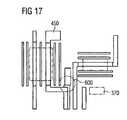
- FIGS. 14-17illustrate the different procedures for the positioning of the scatterbars (SRAF) 550 and the treatment of landing pads.
- optically non-resolvable auxiliary structures 550are not arranged optimally.
- SRAFoptically non-resolvable auxiliary structures
- the region 570optically non-resolvable auxiliary structures 550 are placed in non-parallel fashion along the gate (active structure), as a result of which imaging errors may occur in the case of the CD-critical active structure.
- the wiring structure (passive structure) situated on the right above the gateis, by contrast, erroneously optimally supported by SRAF 550 .
- the “gate first approach” described further below in connection with FIG. 15eliminates this potential defect.
- no SRAF structures 550can be arranged owing to the excessively small distance between the wiring interconnects.
- corrections in accordance with defocus OPCare performed for the structures of the non-active zones.
- the positioning of the optically non-resolvable auxiliary structures 550is performed in another way. This is shown in connection with FIG. 15 .
- the optically non-resolvable auxiliary structures 550are firstly arranged in the region of the active layout regions 430 ′, and only afterward are arranged in the region of the inactive layout regions 440 ′. This ensures that the optically non-resolvable auxiliary structures 550 cannot be arranged defectively in the region of the particularly critical active layout regions 430 ′.
- the problem of effective SRAF positioning in the region 570is eliminated in this way.
- the positioning of the optically non-resolvable auxiliary structures 550 in the region of the active layout region 430 ′may also be referred to as “gate first positioning” since the optically active regions 430 ′ are regularly formed by the gate regions of transistors.
- the SRAF auxiliary structures 550are arranged exclusively in the region of the active layout regions 430 ′ (see FIGS. 16 and 17 ). No SRAF auxiliary structures are positioned in the remaining layout regions 440 ′ (“gate-only” positioning as seventh exemplary embodiment).
- regions 600can be discerned in FIG. 17 that despite the optimization of the mask layout, it is possible for regions 600 to occur in which the inactive layout region 440 ′ make contact with the active layout regions 430 ′ after the OPC method has been carried out.
- These problemsmay occur in isolated fashion since, as explained above, the inactive layout regions 440 ′ are processed by means of a defocus OPC method, so that a certain expanding of lines and/or corners occurs.
- Such regions where contact is mademust be detected, if appropriate in the course of an aftertreatment, for example an automatic or manual aftertreatment, and repaired (eighth exemplary embodiment).
- landing pads 450are preferably likewise subjected to a separate treatment (ninth exemplary embodiment), since customary self-aligned contacts generally cannot be used for landing pads. This is because landing pads regularly have particular overlay requirements since landing pads, on the one hand, must not become too small, in order that contact connection remains possible, and, on the other hand, must not become too large, in order to avoid short circuits (“bridging”) with adjacent wiring structures. Consequently, for landing pads a target OPC method is generally preferable to a defocus OPC method.
- landing padscan be identified by mask layouts being laid one on top of the other; as an alternative, the landing pads can also be identified manually or with the aid of a dead processing system on the basis of their typical geometrical dimensions or on the basis of the specifications of the electrical circuit.
Landscapes
- Physics & Mathematics (AREA)
- General Physics & Mathematics (AREA)
- Preparing Plates And Mask In Photomechanical Process (AREA)
Abstract
Description
- This application claims priority to
German Patent Application 10 2004 047 263.7 which was filed Sep. 24, 2004, and is incorporated herein by reference. - The invention relates to a method for producing a mask layout avoiding imaging errors for a mask.
- It is known that, in lithography methods, imaging errors can occur if the structures to be imaged become very small and have a critical size or a critical distance with respect to one another. The critical size is generally referred to as the “CD” value (CD: critical dimension).
- What is more, imaging errors may occur if structures are arranged so closely next to one another that they mutually influence one another during the imaging. These imaging errors based on “proximity effects” can be reduced by modifying the mask layout beforehand with regard to the “proximity phenomena” that occur. Methods for modifying the mask layout with regard to avoiding proximity effects are referred to by experts by the term OPC methods (OPC: optical proximity correction).
FIG. 1 illustrates a lithography process without OPC correction. The illustration reveals amask 10 with amask layout 20 that is intended to produce a desiredphotoresist structure 25 on awafer 30. Themask layout 20 and the desiredphotoresist structure 25 are identical in the example in accordance withFIG. 1 . Alight beam 40 passes through themask 10 and also a focusinglens 50 arranged downstream and falls onto thewafer 30, thereby imaging themask layout 20 on thewafer 30 coated with photoresist. On account of proximity effects, imaging errors occur in the region of closely adjacent mask structures with the consequence that the resultingphotoresist structure 60 on thewafer 30 in part deviates considerably from themask layout 20 and thus from the desiredphotoresist structure 25. The photoresist structure that results on thewafer 30, the photoresist structure being designated by thereference symbol 60, is illustrated in enlarged fashion and schematically beneath thewafer 30 for improved illustration inFIGS. 1 and 2 .- In order to avoid or to reduce these imaging errors, it is known to use OPC methods that modify the
mask layout 20 beforehand in such a way that the resultingphotoresist structure 60 on thewafer 30 corresponds to the greatest possible extent to the desiredphotoresist structure 25. FIG. 2 shows a previously known OPC method described in the document “A little light magic” (Frank Schellenberg, IEEE Spectrum, September 2003, pages 34 to 39), which is incorporated herein by reference, in which themask layout 20′ is altered compared with theoriginal mask layout 20 in accordance withFIG. 1 . The modifiedmask layout 20′ has structure alterations that are smaller than the optical resolution limit and, therefore, cannot be imaged “1:1”. These structure alterations nevertheless influence the imaging behavior of the mask, as can be discerned at the bottom ofFIG. 2 . This is because the resultingphotoresist structure 60 corresponds distinctly better to the desiredphotoresist structure 25 than is the case with the mask in accordance withFIG. 1 .- In the case of the previously known OPC methods by which a “final” mask layout (see
mask 20′ in accordance withFIG. 2 ) is formed from a provisional auxiliary mask layout (e.g., themask layout 20 in accordance withFIG. 1 ), a distinction is made between so-called “rule-based” and “model-based” OPC methods. - In the case of rule-based OPC methods, the formation of the final mask layout is carried out using rules, in particular tables, defined beforehand. The method disclosed in the two U.S. Pat. Nos. 5,821,014 and 5,242,770 (both of which are incorporated herein by reference), by way of example, may be interpreted as a rule-based OPC method, in the case of which optically non-resolvable auxiliary structures are added to the mask layout according to predetermined fixed rules, in order to achieve a better adaptation of the resulting photoresist structure (
reference symbol 60 in accordance withFIGS. 1 and 2 ) to the desired photoresist structure (reference symbols 25 in accordance withFIGS. 1 and 2 ). In the case of these methods, then, a mask optimization is carried out according to fixed rules. - In model-based OPC methods, a lithography simulation method is carried out, in the course of which the exposure operation is simulated. The simulated resulting photoresist structure is compared with the desired photoresist structure, and the mask layout is varied or modified iteratively until a “final” mask layout is present, which achieves an optimum correspondence between the simulated photoresist structure and the desired photoresist structure. The lithography simulation is carried out with the aid of, for example, a DP-based lithography simulator that is based on a simulation model for the lithography process. For this purpose, the simulation model is determined beforehand by “fitting” or adapting model parameters to experimental data. The model parameters may be determined for example by evaluation of so-called OPC curves for various CD values or structure types. One example of an OPC curve is shown in
FIG. 6 and will be explained in connection with the associated description of the figures. Model-based OPC simulators or OPC simulation programs are commercially available. A description is given of model-based OPC methods for example in the article “Simulation-based proximity correction in high-volume DRAM production” (Werner Fischer, Ines Anke, Giorgio Schweeger, Jörg Thiele; Optical Microlithography VIII, Christopher J. Progler, Editor, Proceedings of SPIE VOL. 4000 (2000), pages 1002 to 1009) and in the German Patent No. DE 101 33 127 C2, both of which are incorporated herein by reference. - Irrespective of whether an OPC method is a model-based or a rule-based OPC method, OPC variants can also differ with regard to their respective optimization aim. By way of example, so-called “target” OPC methods and so-called process window OPC methods, for example “defocus” OPC methods, have different optimization aims.
- The aim of target OPC methods is to hit as accurately as possible the predefined target for the individual geometrical dimensions of the mask structures in the case of correctly complying with all the predefined technological and method conditions (e.g., focus, exposure dose, etc.). Thus, in the case of a target OPC variant it is assumed that all the predefined process parameters are “hit” or set and complied with in an ideal way. In this case, the term “target” is understood to mean the structure size of the main structures to be imaged.
- Since the gate length of transistors is of crucial importance for their electrical behavior, target OPC methods are used in particular for the gate plane of masks. What is disadvantageous in the case of the target OPC variant, however, is that the predefined geometrical dimensions of the mask structures are actually complied with only when the predefined process parameters are complied with in a quasi exact fashion. If fluctuations in the process parameters occur, it is possible for, in some instances, considerable deviations to occur between the desired mask structures or mask dimensions and the actual resulting mask structures or mask dimensions. This may lead, for example, to a tearing away of lines or to a short circuit between lines. The resulting process window is, therefore, generally relatively small in the case of a target OPC method.
- By contrast, process window OPC methods, for example defocus OPC methods, have the aim of making the process window—that is to say the permissible parameter range of the process parameters for the exposure process with the resulting mask—as large as possible in order to ensure that the mask specifications are complied with even in the case of process fluctuations. In this case, with defocus OPC methods it is accepted that the geometrical mask target dimensions are not met exactly. Deviations are, therefore, deliberately accepted in order to enlarge the process window and thus the tolerance range during later use of the mask.
- A defocus OPC method is described for example in the above-mentioned German Patent No. DE 101 33 127. This method involves predefining a “fictitious” defocus value, which is taken as a basis for the simulation of the exposure operation. This defocus value specifies that the resist structure to be exposed with the mask lies somewhat outside the optimum focal plane. In the context of the OPC method, an attempt is made to achieve an optimum imagining behavior of the mask despite the defocusing purportedly present. Thus, an attempt is made to compensate for the imaging error caused by the purported defocusing. This “compensation operation” has the effect of changing the form of the mask layout in such a way that the line structures are made wider and as well a larger distance is produced between two adjacent line structures in each case. As a result, a mask is thus obtained with which, when using a focused exposure, the probability of the formation of wider line structures and the formation of larger distances between respectively adjacent line structures is greater than the probability of the formation of excessively small line structures and the formation of excessively small distances between adjacent line structures.
- In one aspect, the invention improves a method of the type specified in the background to the effect that imaging errors, in particular as a result of proximity effects, are avoided even better than before.
- Accordingly, it is provided according to embodiments of the invention that before carrying out the OPC method, with the provisional auxiliary mask layout, firstly a modified auxiliary mask layout is formed by arranging at least one optically non-resolvable auxiliary structure between two mask structures of the provisional auxiliary mask layout, the optically non-resolvable auxiliary structure being positioned between the two mask structures in a manner dependent on the structure size of the two mask structures. In concrete terms, an eccentric arrangement of the optically non-resolvable auxiliary structure between the two mask structures being effected in the case of differing structure sizes of the two mask structures.
- One advantage of various embodiments of the method according to the invention is that an overall larger process window than in the case of the methods explained in the background is achieved, to be precise independently of the structure size and the structure geometry of the mask structures. In this case, the enlargement of the process window is achieved even when there are very large distances between the mask structures and even when there are very large differences in the structure size of adjacent mask structures. This is because, depending on the distance between the mask structures, the larger or else the smaller mask structure of two different mask structures can limit the process windows. Both effects are minimized according to embodiments of the invention by means of the eccentric positioning of the non-resolvable auxiliary structure.
- A particularly large process window can be obtained, in accordance with one advantageous refinement of the method, if the distance between the two mask structures is additionally taken into account when predefining the eccentric offset with respect to a centrally centered arrangement.
- Preferably, the eccentric offset is chosen to be all the larger, the larger the distance between the two mask structures and the larger the structure size difference between the two mask structures.
- By way of example, the structure width of the two mask structures can be used as the structure size.
- Preferably, the eccentric offset of the optically non-resolvable auxiliary structure is effected in such a way that the optically non-resolvable auxiliary structure is at a smaller distance from the smaller or narrower of the two mask structures than from the larger or wider of the two mask structures. An offset in the direction of the smaller or narrower mask structure is thus effected.
- Moreover, it is regarded as advantageous if, in the case of a distance between the two mask structures above a predefined maximum distance, two or more optically non-resolvable auxiliary structures are arranged between the two mask structures. The arrangement of the two or more optically non-resolvable auxiliary structures is effected asymmetrically and eccentrically in a manner dependent on the structure size of the two mask structures if the structure sizes of the two mask structures differ. Through the use of a plurality of auxiliary structures, imaging errors can be reduced particularly well in the case of large structure spacings.
- Preferably, the existence of lithographically effective elements in the vicinity of the two mask structures is additionally taken into account when predefining the offset. In this case, the existence of lithographically effective elements in the vicinity of the two mask structures is left out of consideration if their distance to the two mask structures or the optically non-resolvable auxiliary structures is greater than a predefined limit distance.
- The optically non-resolvable auxiliary structures may be positioned, for example, with the aid of a table. The table predefines the eccentric offset at least in a manner dependent on the structure widths of the respective two mask structures and the distance between the respective two mask structures.
- As an alternative, the optically non-resolvable auxiliary structures are positioned with the aid of a simulation program.
- Moreover, strips oriented perpendicularly to the respectively assigned mask structures may be added as the optically non-resolvable auxiliary structures. In this case, the perpendicular strips may be arranged for example in groups, in particular to form structures like zebra stripes.
- Preferably, the width of the optically non-resolvable auxiliary structures is chosen in a manner dependent on the distance between the two mask structures and/or the structure widths of the two mask structures.
- As explained in the background, a model-based OPC method or a rule-based OPC method may be used as the OPC method.
- A modified arrangement of the optically non-resolvable auxiliary structures is preferably performed in the case of contact holes in order to achieve an optimum imagining behavior. In this case, adjacent optically non-resolvable auxiliary structures may be connected to one another, for example, to form a communal structure.
- Moreover, it is regarded as advantageous if the mask structures of the provisional auxiliary mask layout are enlarged, in particular widened, or reduced in size to form altered mask structures in accordance with a predefined set of rules. This may be done before or after the non-resolvable auxiliary structures are supplemented. Afterward, the modified auxiliary mask layout is then subjected to the “actual” OPC method, in the course of which the final mask layout is then formed. One advantage of this variant of the method is that an even larger process window for carrying out the lithography method is achieved than is otherwise the case. Moreover, the optically non-resolvable auxiliary structures can be arranged at a greater distance from the assigned main structures than is the case for example with the rule-based OPC methods with optical auxiliary structures that is disclosed in the U.S. patents mentioned above. Therefore, fewer hard mask specifications are to be complied with with regard to the non-resolvable optical auxiliary structures. Moreover, there is a reduced probability of the auxiliary structures being imaged undesirably under unfavorable conditions. Moreover, the lithography method can also be carried out in “overexposure”, thereby reducing the probability of auxiliary structures being imaged undesirably under unfavorable conditions. In particular, fluctuations in the structure widths over the entire mask (CD uniformity) are transferred to the wafer to a lesser extent, which is reflected in a low MEEF (mask error enhancement factor) value. In addition, the auxiliary structures may be wider than in the case of the previously known correction method described in the U.S. patents mentioned above, so that the “process window” is enlarged in this respect, too. The masks thus become easier to produce and less expensive. In addition, on account of the enlargement of the process window, moreover the dependence of the CD value on the main structure, is lower than otherwise, so that photoresist structures that can be produced with the mask react less to process and target fluctuations. This also relates, in particular, to the etching process following the photoresist development, since OPC is often employed after the etching step in the gate contact-connection plane. In other words, the OPC correction is effected in such a way that the CD corresponds to the design value after etching. In this case, the term “target” is understood to mean the structure size of the main structures to be imaged. On account of the enlargement or reduction in size of the mask structures and as a result of the addition of the optical auxiliary structures, already such a distinct improvement in the imaging behavior of the mask is achieved that generally the processing times in the subsequent OPC step are significantly reduced, namely because the deviations between the resulting photoresist structure and the desired photoresist structure are already greatly reduced by the “preoptimization”.
- It is preferably provided that a model-based OPC method is to be carried out as the OPC method—this therefore means the main optimization method is to be carried out after the pre-optimization. The advantage of a model-based OPC method (or OPC simulation program) over a rule-based OPC method is that only relatively few measurement data have to be recorded in order to be able to determine the model parameters required for the method. Afterward, virtually arbitrary structures can then be simulated. In contrast to this, in the case of a rule-based OPC method, comparatively extensive test measurements on the basis of structures that have really been produced are necessary in order to be able to establish the tables or rules required for carrying out the rule-based OPC method.
- With regard to the enlargement or reduction in size of the mask structures—this modification step is referred to hereinafter for short as “pre-bias step”—, it is regarded as advantageous if the set of rules to be employed is stored in the form of a table and the extent of enlargement or reduction in size—that is to say the “pre-bias”—is read from the table for each mask structure of the provisional auxiliary mask layout. On account of the “pre-bias” values being stored in a table, the pre-bias method step can be carried out very rapidly.
- In this case, the discretization of the table values or of the table (=difference between the successive table values) is preferably identical to the discretization of the grid structure (=distance between the grid points) used in the subsequent OPC method, in order to enable an optimum further processing of the structure changes produced in the pre-bias step in the subsequent OPC method. As an alternative, the discretization of the table may also be twice as large as the discretization of the grid structure used in the OPC method, for example when the lines are intended to be “biased” (=enlarged or reduced in size) symmetrically with respect to their line center, since the bias effect respectively always occurs doubly in such a case.
- As an alternative to a set of rules stored in the form of a table, the set of rules may also be stored in a mathematical function, the extent of enlargement or reduction in size—that is to say the pre-bias—of the mask structures of the provisional auxiliary mask layout being calculated for each of the mask structures with the aid of the mathematical function.
- Preferably, the set of rules defines the extent of the enlargement or reduction in size of the mask structures of the provisional auxiliary mask layout in two-dimensional form, so that actual two-dimensional geometrical design structures can be taken into account.
- Moreover, the set of rules takes account of mask structures having dimensions in the CD range separately by defining CD classes with, in each case, a minimum and maximum structure size, and wherein an identical set of rules is employed within each CD class.
- Moreover, the set of rules may provide additional rules to be applied to line ends and contact holes. By way of example, line ends or contact holes are lengthened or shortened or rounded or serif-like structures or so-called hammerheads are added.
- Moreover, the set of rules may deal differently with mask structures that represent wirings and those that define the gate or the gate length of transistors, by virtue of the fact that different sets of rules are employed in each case therefor.
- In addition, the set of rules preferably also takes into account, besides the CD value, the distance between the main structures of the provisional auxiliary mask layout by using a two-dimensional bias matrix, that is to say a bias matrix dependent on the CD value and on the distance.
- The sets of rules used are determined either experimentally on the basis of test structures or by means of lithography simulation.
- In accordance with a further advantageous refinement of the method, it is provided that at least two different OPC variants are used in the context of the OPC method in that the provisional auxiliary mask layout is subdivided into at least two layout regions, and each of the layout regions is processed according to one of the at least two OPC variants. What is thereby achieved is that each of the layout regions is optimized with an individually assigned OPC variant that is particularly suitable in each case for the respective layout region. Consequently, according to the invention, there is no “overall”, mask-embracing identical optimization for all layout regions of the layout, but instead an individual optimization relative to layout regions. What is achieved as a result of this procedure is that after the conclusion of the OPC method, a final mask layout is present with which a particularly high process stability is achieved. In this case, the term “process stability” is understood to mean that, on the one hand, a sufficiently large process window is achieved and, on the other hand, the predefined mask parameters or target parameters are attained in an optimum manner. Moreover, fewer OPC process cycles or OPC passes are regularly required overall until the optimum, final mask layout has been determined than is the case with the previously known “pure” target OPC and “pure” defocus OPC methods. A significant process acceleration is thus additionally achieved on account of the separation of the mask layout into at least two layout regions and the optimization of these layout regions for each of them individually. Furthermore, there is generally no need for a post-processing process. In this case, a post-processing process is understood to mean that mask defects possibly present in the final mask layout are eliminated manually or by means of further optimization programs using DP systems. This is because, on account of the individual optimization in terms of layout regions, the method according to embodiments of the invention in general does not require manual “reworking” of the mask layout, because mask defects occur only seldom enough to be negligible. In addition, it is possible to resort to already known and tried and tested OPC variants. It is necessary merely to carry out a subdivision of layout regions and to select the OPC variant particularly suitable in each case for the respective layout regions of the mask layout.
- Since, as explained above, process window OPC methods, in particular defocus OPC methods, and target OPC methods are already tried and tested in practice, it is regarded as advantageous, in the context of one development of the method, if the method comprises at least one process window OPC variant, in particular a defocus OPC variant, and/or at least one target OPC variant.
- As has already been explained in the background, gate structures of transistors, in particular, are especially critical since with these structures it is particularly important to comply with the predefined geometrical dimensions, in particular the gate length. It is, therefore, regarded as advantageous, in the context of a further development of the method, if the provisional auxiliary mask layout is subdivided into a layout region with active structures and into a layout region with inactive structures, so that particular attention can be given to the specific optimization requirements of the active structures.
- Preferably, the layout region with the active structures is subjected to the target OPC variant and the layout region with the inactive structures is subjected to the defocus OPC variant. In this case, the gate structures of transistors are preferably treated as the active structures.
- The active layout regions can be determined particularly simply and thus advantageously if the provisional auxiliary mask layout and the mask layout—describing the active regions and thus the gate structures—of masks prearranged in terms of layout are “made one above the other” by software or manually, and those regions that lie above active zones—for example diffusion zones—are treated as active structures. The masks that define the diffusion zones, for example, may be used for the “process of laying one above the other”.
- Furthermore, it is regarded as advantageous if transition regions (“buffer zones”) are formed between the active and the inactive layout regions and are optimized separately. The buffer zones may also be assigned to the target OPC variant, for example.
- Both for the defocus OPC variant and for the target OPC variant, it is advantageously possible to select, in each case, either a model-based OPC variant or a rule-based OPC variant; however, model-based variants are preferable in each case.
- Furthermore, it is regarded as advantageous if those layout regions that are provided with the optically non-resolvable auxiliary structures are subjected to a different OPC variant than the layout regions without the optically non-resolvable auxiliary structures. By way of example, the layout regions with the optically non-resolvable auxiliary structures may be subjected to a target OPC variant, and the surrounding layout regions may be subjected to a defocus OPC variant.
- Since the layout regions with the active structures are very critical because the electrical behavior of the later electrical components is generally dependent on these structures, it is regarded as advantageous if firstly the layout regions with the active structures, in particular firstly the layout regions with the gate structures, are supplemented with optically non-resolvable auxiliary structures. It is only if the active structures are provided with the optically non-resolvable auxiliary structures that the remaining layout regions are then also optimized correspondingly.
- Moreover, it is regarded as advantageous if exclusively the active layout regions, in particular exclusively the layout regions with the gate structures, are supplemented with the optically resolvable auxiliary structures. Specifically, this precludes the situation in which optically non-resolvable auxiliary structures for inactive layout regions can impair adjoining active layout regions.
- Furthermore, it is preferably ensured when producing the final mask layout that wiring regions do not lie above active layout regions if the latter are not intended to be contact-connected.
- Moreover, when producing the final mask layout, pad structures (e.g., “landing pads”) and remaining wiring structures are preferably treated differently, since pad structures, on account of the contact-connecting steps subsequently required, are subject to different requirements than the remaining wiring structures. A target OPC variant is preferably used when producing the mask layout for pad structures.
- Furthermore, it is regarded as advantageous if the method is carried out—in particular exclusively—on non-gate planes, for example on RX regions (=diffusion zones in the case of logic chips) and/or on metallization planes.
- Moreover, CD-critical and non-CD-critical structures may advantageously be treated with different OPC variants.
- By way of example, the method can be used for DRAM mask layouts. In this case, cell array structures and cell array edge structures are then preferably processed with different OPC variants. This is because the cell array edge often comprises dummy structures that are not required functionally in electrical terms, thus electrically required mask structures and unrequired dummy structures are preferably treated differently.
- The method according to embodiments of the invention can be carried out particularly simply and rapidly by means of a DP system or by means of a computer.
- For a more complete understanding of the present invention, and the advantages thereof, reference is now made to the following descriptions taken in conjunction with the accompanying drawing, in which:
FIG. 1 shows an illustration of the lithographic process without OPC;FIG. 2 show an illustration of the lithographic process with OPC;FIG. 2A shows an illustration of the dependence of the CD value on the distance between the mask structures among one another (“OPC curve”);FIGS. 3A and 3B show a first exemplary embodiment of the method according to the invention with large distances between the mask structures;FIGS. 4A and 4B show the first exemplary embodiment of the method according to the invention with small distances between the mask structures;FIG. 5 shows a diagram showing the resulting process window for a structure in accordance withFIGS. 3A to4B in the case of a target OPC method;FIG. 6 shows a diagram showing the resulting process window for a structure in accordance withFIGS. 3A to4B in the case of a process window OPC method;FIG. 7 shows diagrams showing, by way of example, a comparison between target OPC and process window OPC methods;FIGS. 8A and 8B show, as a second exemplary embodiment of the method according to the invention, the positioning of a plurality of scatterbars or scatterbar groups (comprising 2, 3 or 4 scatterbars) with small and large distances between the mask structures;FIGS. 9 and 10 show, by way of example, the positioning of non-resolvable auxiliary structures in the vicinity of contact holes (third exemplary embodiment);FIG. 11 shows, by way of example, a structure with a zebra-stripe-like arrangement of the non-resolvable auxiliary structures (fourth exemplary embodiment);FIG. 12 shows, by way of example, a table that predefines the eccentric offset for positioning of the non-resolvable auxiliary structures;FIG. 13 shows a provisional auxiliary mask layout that is processed in accordance with a fifth exemplary embodiment of the method according to the invention;FIG. 14 shows a final mask layout formed from the provisional auxiliary mask layout in accordance withFIG. 13 ;FIG. 15 shows a sixth exemplary embodiment of the method according to the invention, in which optically non-resolvable structures are firstly positioned in active layout regions; andFIGS. 16 and 17 show a seventh, eighth and ninth exemplary embodiment of the method according to the invention, in which optically non-resolvable structures are positioned exclusively in active layout regions, and contact hole charge regions (landing pads) and wiring structures above diffusion zones are treated separately.- The following list of reference symbols can be used in conjunction with the figures:
- 10 Mask
- 20 Mask layout
- 20′ Modified or final mask layout
- 25 Photoresist structure
- 30 Wafer
- 40 Light beam
- 50 Focusing lens
- 60 Resulting photoresist structure
- 70 OPC curve
- 71 Isolated lines
- 72 Semi-dense structures
- 73 Very dense structures
- 100 Provisional auxiliary mask layout
- 100′ Modified auxiliary mask layout
- 110 Narrow structure, “line”
- 120 Wide structure, “line”
- 130 Scatterbar, non-imaging
- 130′Scatterbar group, non-imaging
- 140 Contact holes
- 150 Continuous individual scatterbar
- 200 Useful structure
- 210 Parallel lines, non-imaging
- 220 Perpendicular lines, non-imaging
- 230 Scatterbar, non-imaging
- 240 Zebra structures, non-imaging
- 320 Diffusion zone
- 400 Provisional auxiliary mask layout
- 410 Interconnect structures
- 430 Active structures
- 430′ Active layout regions
- 440 Passive structures
- 440′ Passive layout regions
- 450 Landing pads
- 500 Final mask layout
- 550 SRAF auxiliary structures, non-imaging
- 560 Buffer zone
- 570 Defect region
- 580 Defect region
- 590 External interconnect structure
- 600 Region where contact is made
- V Offset
- ΔB Width difference
- B1, B2 Line width
- A Distance
- M Center
FIG. 2A illustrates anOPC curve 70 specifying how the CD values vary in a manner dependent on the distance between the main structures, for example thus in the case of lines. In the case ofisolated lines 71, the CD value is largely independent of the distance between the structures. In the case of average, semi-densemain structures 72, the CD value falls in the direction of smaller structure distances before it rises significantly again in the case of verydense structures 73.- In this case, the
OPC curve 70 describes the CD value profile on the wafer given a constant mask CD value, which is likewise depicted inFIG. 2A for comparison. FIGS. 3A and 3B show, by way of example, the eccentric arrangement according to the invention of optically non-resolvable auxiliary structures (first exemplary embodiment).FIG. 3A reveals a provisionalauxiliary mask layout 100 comprising two lines (or bars)110 and120 arranged at a distance A. The two lines have different structures widths B1 and B2. Ascatterbar 130 is added as an optically non-resolvable auxiliary structure between the twolines FIG. 3A , thescatterbar 130 is offset by an offset V relative to the centre M between the twobars
ΔB=B1−B2
and the distance A between the lines and can be gathered for example from the table inFIG. 12 . The offset V is thus a function of the following variables:
V=f(ΔB, A)- As an alternative, the absolute values of the widths may also have an influence in addition. In this case, then, the offset V would be a function of the following variables:
V=f(ΔB, B1,B2,A) - After the eccentric positioning of the
scatterbar 130, themask structures FIG. 12 , in which the offset values V for the eccentric positioning of thescatterbar 130 are entered. In the table inFIG. 12 and also inFIG. 3B , the widening values are designated by ΔB1 for the “widening” of the width B1 of thebar 110 and ΔB2 for the for the “widening” of the width B2 of theline 120. FIG. 3B shows the resulting modifiedauxiliary mask layout 100′ comprising thelines scatterbar 130. It can be discerned that the distance A′ between the twolines - In the exemplary table in
FIG. 12 , the width of thescatterbars 130 has been assumed to be constant (width=40 nm); it goes without saying that scatterbar widths other than 40 nm could also be taken into account in the table, so that the table would need to be extended accordingly. Offset values V for 300 nm<A<380 nm, B1=100 nm and B2=200 nm are entered in the table inFIG. 12 . The table can also be made more comprehensive and take account of the following ranges of values, for example: 300 nm<A<1000 nm, 100 nm<B1, B2<400 nm. FIGS. 4A and 4B show the addition of ascatterbar 130 for the case where the distance A between the twolines scatterbar 130 is eccentric, the offset V is relatively small. Thus, it is preferred for a small offset value V to be chosen in the case of small distances A and for a large offset value to be chosen in the case of large distances A if the twolines FIG. 5 shows a diagram specifying the optimum offset V in each case for the twoauxiliary mask layouts 100 shown inFIGS. 3A to4B. The diagram illustrates a defocus value DOF (=depth of focus) in μm for an EDL value (=exposure dose latitude) of 7%; the offset V at which the largest process window (PW) is attained can thus be read from the diagram. The diagram in accordance withFIG. 5 takes account of the case where a target OPC is subsequently carried out in order to form the final mask layout.- The diagram in
FIG. 5 is based on the following parameters for the structure100: - Width B1=100 nm
- Width B2=200 nm
- Width of the scatterbar=40 nm
- Minimum distance Aminbetween the lines=300 nm
- Maximum distance Amaxbetween the lines=400 nm
- OPC grid=2.5 nm
- Moreover, the assumption is made in the diagram that an anchor structure comprising a multiplicity of parallel lines having a line width of 90 nm and a line spacing of 120 nm is present besides the
structure 100 illustrated inFIGS. 3A to4B. - It can be discerned that when there is a small distance of only 300 nm between the
lines scatterbar 130 is optimally positioned near the center M; the offset V is therefore very small (V=approximately −5 nm). When there is a large distance of 400 nm between the twolines scatterbar 130 is highly eccentric, to be precise with an offset of approximately V=−30 nm (offset in the direction of the narrower lines110). FIG. 6 shows a corresponding diagram for the case where a process window OPC (PW-OPC) for forming the final mask layout is carried after the positioning of thescatterbar 130 and the widening of the two line widths B1 and B2.- It is evident that when there is a small distance A=300 nm between the two
lines scatterbar 130 lies distinctly in the eccentric region. An optimum offset V of approximately −40 nm can be read; a maximum process window size is achieved with this offset because the DOF value and thus the maximum permissible defocusing when processing the mask structures assumes its largest value (DOF=0.42 μm). - The diagrams in
FIGS. 5 and 6 do not reveal whether the “useful structure”100 or the anchor structure that is likewise taken into account as has already been mentioned above limits the process window, because the resulting process window is specified for the overall structure. The elements that limit the process window are additionally plotted inFIG. 7 . - The left-hand diagram of
FIG. 7 shows the process window for a target OPC (lower line) and for a process window OPC (upper line) for the case of a maximum bar distance A=400 nm. Thenarrower line 110 limits the process window over the entire offset range ΔV1 (−55 nm<V<20 m). - The right-hand diagram of
FIG. 7 shows the process window for a target OPC (lower line) and a process window OPC (upper line) for the case of a minimum bar distance A=300 nm. Thenarrower bar 110 limits the process window in the offset range ΔV2 (−30 nm<V<−20 nm). Thewider bar 120 limits the process window in the offset range ΔV3 (−20 nm<V<5 nm), both the anchor structure and thewider line 120 equally limiting the process window for the special case V4=−5 nm. FIGS. 8A and 8B show the eccentric arrangement ofscatterbars 130 for the case where two or more scatterbars130 are to be arranged on account of the large distance A between the twolines 110 and120 (second exemplary embodiment). It is evident in both figures that when there are two or more scatterbars130, the resultingscatterbar group 130′ is jointly offset; a “group offset” as it were is effected, the offset V of thescatterbar group 130′ being determined according to criteria explained above.FIG. 8A shows that the arrangement of thescatterbar group 130′ is effected only slightly eccentrically when there are small distances A between the twolines FIG. 8B , the offset of thescatterbar group 130′ is distinctly larger. In the bottommost structure inFIG. 8B , the distance between the two lines is so large that twoseparate scatterbar groups 130′ are formed, which are in each case assigned only to one of the two lines. The twobars FIGS. 9 and 10 show the arrangement ofscatterbars 130 by way of example for the case ofcontact holes 140 as useful structure or “provisional auxiliary mask layout”100 (third exemplary embodiment). Only the scatterbars between the rows of contact holes are illustrated. It is evident that thescatterbars 130 can be arranged separately (seeFIG. 9 ) or can be formed by a continuousindividual scatterbar 150.FIG. 11 shows a relatively complexuseful structure 200 that forms a provisional auxiliary mask layout. Theuseful structure 200 comprisesparallel lines 210 having different widths and at different distances (four exemplary embodiment). Depending on the distance,scatterbars scatterbars 230 thus form “zebra structures”240 that modify the provisional auxiliary mask layout. Thezebra structures 240 are preferably used in the case of medium to large line distances for which, in the case of usingparallel scatterbars 220, it would be necessary to arrange two or more parallel scatterbars. The advantage of thezebra structures 240 is that they improve the so-called MEEF (Mask Error Enhancement Factor).- A fifth exemplary embodiment of the method according to the invention will now be explained in connection with
FIGS. 13 and 14 . FIG. 13 shows a provisionalauxiliary mask layout 400, which defines metallization structures orinterconnect structures 410. Theinterconnect structures 410 are predefined by an electrical circuit diagram.- The provisional
auxiliary mask layout 400 hasactive layout regions 430′ foractive structures 430 and also inactive orpassive layout regions 440′ for inactive orpassive structures 440. In this case, as already explained above, theactive layout regions 430′ are understood to be those layout regions of the provisionalauxiliary mask layout 400 that are arranged above the active zones of the electrical circuit. Active zones are formed for example by the diffusion zones of transistors that are contact-connected by means of theactive layout regions 430′ of theauxiliary mask layout 400. - The
inactive layout regions 440′ are understood to be those layout regions that are arranged outside active zones and thus essentially form connections between theactive layout regions 430′ or to external terminal pads (“landing pads” or contact hole landing points)450. - Prior to carrying out an OPC method, in a first preparatory step, the provisional
auxiliary mask layout 400 is subdivided into theactive layout regions 430′ and into the passive orinactive layout regions 440′ in order that these can be treated differently. - In order to ascertain which layout regions of the provisional
auxiliary mask layout 400 are active layout regions and which are inactive layout regions, the provisionalauxiliary mask layout 400 is laid over the mask layouts of the prearranged masks—that is to say over the mask layouts of those masks that are processed prior to the mask with themask layout 400 in accordance withFIG. 14 . The process of laying the mask layouts of different mask planes one on top of the other can be effected manually or preferably with the aid of an electronic data processing system. The regions in which interconnect structures lie above diffusion zones can be discerned as a result of the masks being laid one on top of the other. The zones are regarded hereinafter as theactive layout regions 430′. - Those layout regions of the provisional
auxiliary mask layout 400 that lie above active zones (transistor zones, in particular diffusion zones or gate regions of transistors, etc.) are thus identified asactive layout regions 430′. The remaining layout regions are identified asinactive layout regions 440′. - With the provisional
auxiliary mask layout 400, afinal mask layout 500 is then formed.FIG. 14 in this case shows the mask layout after optically non-resolvable SRAF auxiliary structures have been added to the mask layout, more or less eccentrically depending on the structure. The structure segmentation that usually occurs is not illustrated inFIG. 14 for reasons of clarity. - When the subsequent OPC method is carried out, the
active layout regions 430′ and thepassive layout regions 440′ are treated differently since the active layout regions and the passive layout regions are subject to different tolerance requirements. In concrete terms, thelayout regions 430′ with theactive structures 430 are subjected to a target OPC method (or a target OPC variant), whereas thelayout regions 440′ with thepassive structures 440 are optimized by means of a defocus OPC method (or defocus OPC variant). Buffer zones 560 may furthermore be formed in the boundary regions between theactive layout regions 430′ and theinactive layout regions 440′, the buffer zones optionally being treated like theactive layout regions 430′, like thepassive layout regions 440′ or in accordance with a dedicated optimization method. Thebuffer zones 560 serve to take account of, and as far as possible to compensate for, overlay fluctuations or the offset of different lithography planes with respect to one another.FIGS. 14-17 illustrate the different procedures for the positioning of the scatterbars (SRAF)550 and the treatment of landing pads.- As can be discerned in
FIG. 14 , in the case of conventional positioning of the optically non-resolvableauxiliary structures 550, it is possible to discern regions in which the optically non-resolvable auxiliary structures (SRAF)550 are not arranged optimally. By way of example, in theregion 570 optically non-resolvableauxiliary structures 550 are placed in non-parallel fashion along the gate (active structure), as a result of which imaging errors may occur in the case of the CD-critical active structure. The wiring structure (passive structure) situated on the right above the gate is, by contrast, erroneously optimally supported bySRAF 550. The “gate first approach” described further below in connection withFIG. 15 eliminates this potential defect. - In a
different region 580 ofFIG. 14 , noSRAF structures 550 can be arranged owing to the excessively small distance between the wiring interconnects. In thisregion 580, corrections in accordance with defocus OPC (or some other process window OPC variant) are performed for the structures of the non-active zones. - In accordance with a sixth exemplary embodiment of the method according to the invention, the positioning of the optically non-resolvable
auxiliary structures 550 is performed in another way. This is shown in connection withFIG. 15 . - It is evident that, in the sixth exemplary embodiment in accordance with
FIG. 15 the optically non-resolvableauxiliary structures 550 are firstly arranged in the region of theactive layout regions 430′, and only afterward are arranged in the region of theinactive layout regions 440′. This ensures that the optically non-resolvableauxiliary structures 550 cannot be arranged defectively in the region of the particularly criticalactive layout regions 430′. By way of example, the problem of effective SRAF positioning in the region570 (seeFIG. 14 ) is eliminated in this way. - The positioning of the optically non-resolvable
auxiliary structures 550 in the region of theactive layout region 430′ may also be referred to as “gate first positioning” since the opticallyactive regions 430′ are regularly formed by the gate regions of transistors. - In a seventh exemplary embodiment of the method, the SRAF
auxiliary structures 550 are arranged exclusively in the region of theactive layout regions 430′ (seeFIGS. 16 and 17 ). No SRAF auxiliary structures are positioned in the remaininglayout regions 440′ (“gate-only” positioning as seventh exemplary embodiment). - It can be discerned in
FIG. 17 that despite the optimization of the mask layout, it is possible forregions 600 to occur in which theinactive layout region 440′ make contact with theactive layout regions 430′ after the OPC method has been carried out. These problems may occur in isolated fashion since, as explained above, theinactive layout regions 440′ are processed by means of a defocus OPC method, so that a certain expanding of lines and/or corners occurs. Such regions where contact is made must be detected, if appropriate in the course of an aftertreatment, for example an automatic or manual aftertreatment, and repaired (eighth exemplary embodiment). - It can additionally be discerned in
FIG. 17 that theselanding pads 450 are preferably likewise subjected to a separate treatment (ninth exemplary embodiment), since customary self-aligned contacts generally cannot be used for landing pads. This is because landing pads regularly have particular overlay requirements since landing pads, on the one hand, must not become too small, in order that contact connection remains possible, and, on the other hand, must not become too large, in order to avoid short circuits (“bridging”) with adjacent wiring structures. Consequently, for landing pads a target OPC method is generally preferable to a defocus OPC method. - Just like the active layout regions, landing pads can be identified by mask layouts being laid one on top of the other; as an alternative, the landing pads can also be identified manually or with the aid of a dead processing system on the basis of their typical geometrical dimensions or on the basis of the specifications of the electrical circuit.
Claims (50)
Applications Claiming Priority (2)
| Application Number | Priority Date | Filing Date | Title |
|---|---|---|---|
| DE102004047263ADE102004047263B4 (en) | 2004-09-24 | 2004-09-24 | A method of generating an aberration avoiding mask layout for a mask |
| DE102004047263.7 | 2004-09-24 |
Publications (2)
| Publication Number | Publication Date |
|---|---|
| US20060070018A1true US20060070018A1 (en) | 2006-03-30 |
| US7346885B2 US7346885B2 (en) | 2008-03-18 |
Family
ID=36011664
Family Applications (1)
| Application Number | Title | Priority Date | Filing Date |
|---|---|---|---|
| US11/233,927Expired - Fee RelatedUS7346885B2 (en) | 2004-09-24 | 2005-09-23 | Method for producing a mask layout avoiding imaging errors for a mask |
Country Status (2)
| Country | Link |
|---|---|
| US (1) | US7346885B2 (en) |
| DE (1) | DE102004047263B4 (en) |
Cited By (33)
| Publication number | Priority date | Publication date | Assignee | Title |
|---|---|---|---|---|
| US20070162887A1 (en)* | 2005-10-28 | 2007-07-12 | Sung-Soo Suh | Method of fabricating photo mask |
| US20070264584A1 (en)* | 2006-02-13 | 2007-11-15 | Samsung Electronics Co., Ltd. | Pattern arrangement method of semiconductor device |
| US20080010628A1 (en)* | 2006-07-10 | 2008-01-10 | Sung-Gon Jung | Method of manufacturing a mask |
| US20080222587A1 (en)* | 2007-03-05 | 2008-09-11 | Tela Innovations, Inc. | Integrated Circuit Cell Library for Multiple Patterning |
| US20090029267A1 (en)* | 2007-07-24 | 2009-01-29 | Cho Kuo-Yao | Photomask layout pattern |
| US20090064084A1 (en)* | 2007-09-05 | 2009-03-05 | United Microelectronics Corp. | Prediction model and prediction method for exposure dose |
| US20100011333A1 (en)* | 2006-03-09 | 2010-01-14 | Tela Innovations, Inc. | Semiconductor Device Layout Having Restricted Layout Region Including Linear Shaped Gate Electrode Layout Features Defined with Minimum End-to-End Spacing and At Least Eight Transistors |
| US20100187633A1 (en)* | 2008-03-13 | 2010-07-29 | Tela Innovations, Inc. | Channelized Gate Level Cross-Coupled Transistor Device with Cross-Coupled Transistors Defined on Two Gate Electrode Tracks with Crossing Gate Electrode Connections |
| US20110179391A1 (en)* | 2010-01-19 | 2011-07-21 | International Business Machines Corporation | Leakage aware design post-processing |
| US20110175144A1 (en)* | 2007-08-02 | 2011-07-21 | Tela Innovations, Inc. | Integrated Circuit Device Including Dynamic Array Section with Gate Level Having Linear Conductive Features on at Least Three Side-by-Side Lines and Uniform Line End Spacings |
| US8214778B2 (en) | 2007-08-02 | 2012-07-03 | Tela Innovations, Inc. | Methods for cell phasing and placement in dynamic array architecture and implementation of the same |
| US8225261B2 (en) | 2006-03-09 | 2012-07-17 | Tela Innovations, Inc. | Methods for defining contact grid in dynamic array architecture |
| US8225239B2 (en) | 2006-03-09 | 2012-07-17 | Tela Innovations, Inc. | Methods for defining and utilizing sub-resolution features in linear topology |
| US8245180B2 (en) | 2006-03-09 | 2012-08-14 | Tela Innovations, Inc. | Methods for defining and using co-optimized nanopatterns for integrated circuit design and apparatus implementing same |
| US8247846B2 (en) | 2006-03-09 | 2012-08-21 | Tela Innovations, Inc. | Oversized contacts and vias in semiconductor chip defined by linearly constrained topology |
| US8286107B2 (en) | 2007-02-20 | 2012-10-09 | Tela Innovations, Inc. | Methods and systems for process compensation technique acceleration |
| US8448102B2 (en) | 2006-03-09 | 2013-05-21 | Tela Innovations, Inc. | Optimizing layout of irregular structures in regular layout context |
| US8453094B2 (en) | 2008-01-31 | 2013-05-28 | Tela Innovations, Inc. | Enforcement of semiconductor structure regularity for localized transistors and interconnect |
| US8471391B2 (en) | 2008-03-27 | 2013-06-25 | Tela Innovations, Inc. | Methods for multi-wire routing and apparatus implementing same |
| US8541879B2 (en) | 2007-12-13 | 2013-09-24 | Tela Innovations, Inc. | Super-self-aligned contacts and method for making the same |
| US8572522B2 (en) | 2011-09-16 | 2013-10-29 | Imec | Illumination-source shape definition in optical lithography |
| US8653857B2 (en) | 2006-03-09 | 2014-02-18 | Tela Innovations, Inc. | Circuitry and layouts for XOR and XNOR logic |
| US8661392B2 (en) | 2009-10-13 | 2014-02-25 | Tela Innovations, Inc. | Methods for cell boundary encroachment and layouts implementing the Same |
| US8658542B2 (en) | 2006-03-09 | 2014-02-25 | Tela Innovations, Inc. | Coarse grid design methods and structures |
| US8680626B2 (en) | 2007-10-26 | 2014-03-25 | Tela Innovations, Inc. | Methods, structures, and designs for self-aligning local interconnects used in integrated circuits |
| US20140215417A1 (en)* | 2012-01-18 | 2014-07-31 | International Business Machines Corporation | Near-neighbor trimming of dummy fill shapes with built-in optical proximity corrections for semiconductor applications |
| US8839175B2 (en) | 2006-03-09 | 2014-09-16 | Tela Innovations, Inc. | Scalable meta-data objects |
| US8863063B2 (en) | 2009-05-06 | 2014-10-14 | Tela Innovations, Inc. | Finfet transistor circuit |
| US9035359B2 (en) | 2006-03-09 | 2015-05-19 | Tela Innovations, Inc. | Semiconductor chip including region including linear-shaped conductive structures forming gate electrodes and having electrical connection areas arranged relative to inner region between transistors of different types and associated methods |
| US9122832B2 (en) | 2008-08-01 | 2015-09-01 | Tela Innovations, Inc. | Methods for controlling microloading variation in semiconductor wafer layout and fabrication |
| US9159627B2 (en) | 2010-11-12 | 2015-10-13 | Tela Innovations, Inc. | Methods for linewidth modification and apparatus implementing the same |
| US9230910B2 (en) | 2006-03-09 | 2016-01-05 | Tela Innovations, Inc. | Oversized contacts and vias in layout defined by linearly constrained topology |
| US9563733B2 (en) | 2009-05-06 | 2017-02-07 | Tela Innovations, Inc. | Cell circuit and layout with linear finfet structures |
Families Citing this family (4)
| Publication number | Priority date | Publication date | Assignee | Title |
|---|---|---|---|---|
| CN102610606B (en)* | 2005-04-26 | 2016-01-27 | 瑞萨电子株式会社 | Semiconductor device and manufacture method, optical proximity processing method |
| US7979815B2 (en)* | 2008-01-08 | 2011-07-12 | International Business Machines Corporation | Compact model methodology for PC landing pad lithographic rounding impact on device performance |
| US7984395B2 (en)* | 2008-01-17 | 2011-07-19 | Synopsys, Inc. | Hierarchical compression for metal one logic layer |
| KR100934865B1 (en)* | 2008-07-17 | 2009-12-31 | 주식회사 하이닉스반도체 | Separation method of design pattern layout and manufacturing method of exposure mask using same |
Citations (18)
| Publication number | Priority date | Publication date | Assignee | Title |
|---|---|---|---|---|
| US5242770A (en)* | 1992-01-16 | 1993-09-07 | Microunity Systems Engineering, Inc. | Mask for photolithography |
| US5821014A (en)* | 1997-02-28 | 1998-10-13 | Microunity Systems Engineering, Inc. | Optical proximity correction method for intermediate-pitch features using sub-resolution scattering bars on a mask |
| US6077310A (en)* | 1995-12-22 | 2000-06-20 | Kabushiki Kaisha Toshiba | Optical proximity correction system |
| US6114071A (en)* | 1997-11-24 | 2000-09-05 | Asml Masktools Netherlands B.V. | Method of fine feature edge tuning with optically-halftoned mask |
| US20020091985A1 (en)* | 2001-01-05 | 2002-07-11 | Liebmann Lars W. | Method to determine optical proximity correction and assist feature rules which account for variations in mask dimensions |
| US6421820B1 (en)* | 1999-12-13 | 2002-07-16 | Infineon Technologies Ag | Semiconductor device fabrication using a photomask with assist features |
| US20020182523A1 (en)* | 2001-06-05 | 2002-12-05 | Beate Frankowsky | Method for carrying out a rule-based optical proximity correction with simultaneous scatter bar insertion |
| US20020192570A1 (en)* | 2001-03-14 | 2002-12-19 | Smith Bruce W. | Optical proximity correction method utilizing ruled ladder bars as sub-resolution assist features |
| US20040023132A1 (en)* | 2002-06-05 | 2004-02-05 | Seiko Epson Corporation | Photomask, pattern production method, and semiconductor device |
| US20040139418A1 (en)* | 2002-07-26 | 2004-07-15 | Xuelong Shi | Automatic optical proximity correction (OPC) rule generation |
| US20040166418A1 (en)* | 2003-02-21 | 2004-08-26 | International Business Machines Corporation | Method of optical proximity correction with sub-resolution assists |
| US20040248016A1 (en)* | 2003-06-06 | 2004-12-09 | Lucas Kevin D. | Method of designing a reticle and forming a semiconductor device therewith |
| US20040256356A1 (en)* | 2001-08-31 | 2004-12-23 | Lothar Bauch | Photolithographic mask |
| US20050044513A1 (en)* | 2002-01-31 | 2005-02-24 | Robles Juan Andres Torres | Contrast based resolution enhancement for photolithographic processing |
| US20050202321A1 (en)* | 2004-03-10 | 2005-09-15 | International Business Machines Corporation | Pliant sraf for improved performance and manufacturability |
| US20060057475A1 (en)* | 2003-02-28 | 2006-03-16 | Liebmann Lars W | Binary OPC for assist feature layout optimization |
| US20060101370A1 (en)* | 2004-11-05 | 2006-05-11 | International Business Machines Corporation | Method for improving optical proximity correction |
| US20060190919A1 (en)* | 2005-02-24 | 2006-08-24 | Texas Instruments Incorporated | Method of locating sub-resolution assist feature(s) |
Family Cites Families (3)
| Publication number | Priority date | Publication date | Assignee | Title |
|---|---|---|---|---|
| JPH06242594A (en)* | 1993-02-15 | 1994-09-02 | Sharp Corp | Mask for deformed illuminating exposure device |
| DE10133127C2 (en) | 2001-07-07 | 2003-06-26 | Infineon Technologies Ag | Process for producing an exposure mask and process for optimizing a simulation process |
| WO2003021353A1 (en) | 2001-08-31 | 2003-03-13 | Infineon Technologies Ag | Photolithographic mask |
- 2004
- 2004-09-24DEDE102004047263Apatent/DE102004047263B4/ennot_activeExpired - Fee Related
- 2005
- 2005-09-23USUS11/233,927patent/US7346885B2/ennot_activeExpired - Fee Related
Patent Citations (18)
| Publication number | Priority date | Publication date | Assignee | Title |
|---|---|---|---|---|
| US5242770A (en)* | 1992-01-16 | 1993-09-07 | Microunity Systems Engineering, Inc. | Mask for photolithography |
| US6077310A (en)* | 1995-12-22 | 2000-06-20 | Kabushiki Kaisha Toshiba | Optical proximity correction system |
| US5821014A (en)* | 1997-02-28 | 1998-10-13 | Microunity Systems Engineering, Inc. | Optical proximity correction method for intermediate-pitch features using sub-resolution scattering bars on a mask |
| US6114071A (en)* | 1997-11-24 | 2000-09-05 | Asml Masktools Netherlands B.V. | Method of fine feature edge tuning with optically-halftoned mask |
| US6421820B1 (en)* | 1999-12-13 | 2002-07-16 | Infineon Technologies Ag | Semiconductor device fabrication using a photomask with assist features |
| US20020091985A1 (en)* | 2001-01-05 | 2002-07-11 | Liebmann Lars W. | Method to determine optical proximity correction and assist feature rules which account for variations in mask dimensions |
| US20020192570A1 (en)* | 2001-03-14 | 2002-12-19 | Smith Bruce W. | Optical proximity correction method utilizing ruled ladder bars as sub-resolution assist features |
| US20020182523A1 (en)* | 2001-06-05 | 2002-12-05 | Beate Frankowsky | Method for carrying out a rule-based optical proximity correction with simultaneous scatter bar insertion |
| US20040256356A1 (en)* | 2001-08-31 | 2004-12-23 | Lothar Bauch | Photolithographic mask |
| US20050044513A1 (en)* | 2002-01-31 | 2005-02-24 | Robles Juan Andres Torres | Contrast based resolution enhancement for photolithographic processing |
| US20040023132A1 (en)* | 2002-06-05 | 2004-02-05 | Seiko Epson Corporation | Photomask, pattern production method, and semiconductor device |
| US20040139418A1 (en)* | 2002-07-26 | 2004-07-15 | Xuelong Shi | Automatic optical proximity correction (OPC) rule generation |
| US20040166418A1 (en)* | 2003-02-21 | 2004-08-26 | International Business Machines Corporation | Method of optical proximity correction with sub-resolution assists |
| US20060057475A1 (en)* | 2003-02-28 | 2006-03-16 | Liebmann Lars W | Binary OPC for assist feature layout optimization |
| US20040248016A1 (en)* | 2003-06-06 | 2004-12-09 | Lucas Kevin D. | Method of designing a reticle and forming a semiconductor device therewith |
| US20050202321A1 (en)* | 2004-03-10 | 2005-09-15 | International Business Machines Corporation | Pliant sraf for improved performance and manufacturability |
| US20060101370A1 (en)* | 2004-11-05 | 2006-05-11 | International Business Machines Corporation | Method for improving optical proximity correction |
| US20060190919A1 (en)* | 2005-02-24 | 2006-08-24 | Texas Instruments Incorporated | Method of locating sub-resolution assist feature(s) |
Cited By (194)
| Publication number | Priority date | Publication date | Assignee | Title |
|---|---|---|---|---|
| US20070162887A1 (en)* | 2005-10-28 | 2007-07-12 | Sung-Soo Suh | Method of fabricating photo mask |
| US7475383B2 (en)* | 2005-10-28 | 2009-01-06 | Samsung Electronics Co. Ltd. | Method of fabricating photo mask |
| US20070264584A1 (en)* | 2006-02-13 | 2007-11-15 | Samsung Electronics Co., Ltd. | Pattern arrangement method of semiconductor device |
| US8253173B2 (en) | 2006-03-09 | 2012-08-28 | Tela Innovations, Inc. | Semiconductor device with gate level including four transistors of first type and four transistors of second type separated by non-diffusion region and having at least two gate contacts positioned outside separating non-diffusion region |
| US10141335B2 (en) | 2006-03-09 | 2018-11-27 | Tela Innovations, Inc. | Semiconductor CIP including region having rectangular-shaped gate structures and first metal structures |
| US20100006950A1 (en)* | 2006-03-09 | 2010-01-14 | Tela Innovations, Inc. | Semiconductor Device Portion Having Gate Electrode Conductive Structures Formed from Rectangular Shaped Gate Electrode Layout Features and Having At Least Eight Transistors |
| US20100017769A1 (en)* | 2006-03-09 | 2010-01-21 | Tela Innovations, Inc. | Layout of Cell of Semiconductor Device Having Rectangular Shaped Gate Electrode Layout Features and Equal Number of PMOS and NMOS Transistors |
| US8823062B2 (en) | 2006-03-09 | 2014-09-02 | Tela Innovations, Inc. | Integrated circuit with offset line end spacings in linear gate electrode level |
| US20100012982A1 (en)* | 2006-03-09 | 2010-01-21 | Tela Innovations, Inc. | Semiconductor Device Portion Having Sub-Wavelength-Sized Gate Electrode Conductive Structures Formed from Linear Shaped Gate Electrode Layout Features Defined Along At Least Four Gate Electrode Tracks with Minimum End-to-End Spacing and Having Corresponding Non-Symmetric Diffusion Regions |
| US20100017771A1 (en)* | 2006-03-09 | 2010-01-21 | Tela Innovations, Inc. | Layout of Cell of Semiconductor Device Having Rectangular Shaped Gate Electrode Layout Features and At Least Eight Transistors |
| US20100032722A1 (en)* | 2006-03-09 | 2010-02-11 | Tela Innovations, Inc. | Semiconductor Device Portion Having Gate Electrode Conductive Structures Formed from Linear Shaped Gate Electrode Layout Features Defined with Minimum End-to-End Spacing and Having At Least Eight Transistors |
| US8921896B2 (en) | 2006-03-09 | 2014-12-30 | Tela Innovations, Inc. | Integrated circuit including linear gate electrode structures having different extension distances beyond contact |
| US8921897B2 (en) | 2006-03-09 | 2014-12-30 | Tela Innovations, Inc. | Integrated circuit with gate electrode conductive structures having offset ends |
| US8946781B2 (en) | 2006-03-09 | 2015-02-03 | Tela Innovations, Inc. | Integrated circuit including gate electrode conductive structures with different extension distances beyond contact |
| US8952425B2 (en) | 2006-03-09 | 2015-02-10 | Tela Innovations, Inc. | Integrated circuit including at least four linear-shaped conductive structures having extending portions of different length |
| US9009641B2 (en) | 2006-03-09 | 2015-04-14 | Tela Innovations, Inc. | Circuits with linear finfet structures |
| US9035359B2 (en) | 2006-03-09 | 2015-05-19 | Tela Innovations, Inc. | Semiconductor chip including region including linear-shaped conductive structures forming gate electrodes and having electrical connection areas arranged relative to inner region between transistors of different types and associated methods |
| US9230910B2 (en) | 2006-03-09 | 2016-01-05 | Tela Innovations, Inc. | Oversized contacts and vias in layout defined by linearly constrained topology |
| US9240413B2 (en) | 2006-03-09 | 2016-01-19 | Tela Innovations, Inc. | Methods, structures, and designs for self-aligning local interconnects used in integrated circuits |
| US9336344B2 (en) | 2006-03-09 | 2016-05-10 | Tela Innovations, Inc. | Coarse grid design methods and structures |
| US9425145B2 (en) | 2006-03-09 | 2016-08-23 | Tela Innovations, Inc. | Oversized contacts and vias in layout defined by linearly constrained topology |
| US10230377B2 (en) | 2006-03-09 | 2019-03-12 | Tela Innovations, Inc. | Circuitry and layouts for XOR and XNOR logic |
| US8658542B2 (en) | 2006-03-09 | 2014-02-25 | Tela Innovations, Inc. | Coarse grid design methods and structures |
| US10217763B2 (en) | 2006-03-09 | 2019-02-26 | Tela Innovations, Inc. | Semiconductor chip having region including gate electrode features of rectangular shape on gate horizontal grid and first-metal structures of rectangular shape on at least eight first-metal gridlines of first-metal vertical grid |
| US8058671B2 (en) | 2006-03-09 | 2011-11-15 | Tela Innovations, Inc. | Semiconductor device having at least three linear-shaped electrode level conductive features of equal length positioned side-by-side at equal pitch |
| US8072003B2 (en) | 2006-03-09 | 2011-12-06 | Tela Innovations, Inc. | Integrated circuit device and associated layout including two pairs of co-aligned complementary gate electrodes with offset gate contact structures |
| US8089098B2 (en) | 2006-03-09 | 2012-01-03 | Tela Innovations, Inc. | Integrated circuit device and associated layout including linear gate electrodes of different transistor types next to linear-shaped non-gate conductive segment |
| US8089104B2 (en) | 2006-03-09 | 2012-01-03 | Tela Innovations, Inc. | Integrated circuit with gate electrode level region including multiple linear-shaped conductive structures forming gate electrodes of transistors and including uniformity extending portions of different size |
| US8089102B2 (en) | 2006-03-09 | 2012-01-03 | Tela Innovations, Inc. | Method for fabricating integrated circuit having three or more linear-shaped gate electrode level conductive segments of both equal length and equal pitch |
| US8088681B2 (en) | 2006-03-09 | 2012-01-03 | Tela Innovations, Inc. | Method for fabricating integrated circuit including separated diffusion regions of different type each having four gate electrodes with each of two complementary gate electrode pairs formed from respective linear condcutive segment |
| US8089099B2 (en) | 2006-03-09 | 2012-01-03 | Tela Innovations, Inc, | Integrated circuit device and associated layout including gate electrode level region of 965 NM radius with linear-shaped conductive segments on fixed pitch |
| US8088682B2 (en) | 2006-03-09 | 2012-01-03 | Tela Innovations, Inc. | Method for fabricating integrated circuit with gate electrode level region including two side-by-side ones of at least three linear-shaped conductive structures electrically connected to each other through non-gate level |
| US8089100B2 (en) | 2006-03-09 | 2012-01-03 | Tela Innovations, Inc. | Integrated circuit with gate electrode level region including at least four linear-shaped conductive structures forming gate electrodes of transistors and including extending portions of at least two different sizes |
| US8088680B2 (en) | 2006-03-09 | 2012-01-03 | Tela Innovations, Inc. | Method for fabricating integrated circuit having at least three linear-shaped gate electrode level conductive features of equal length positioned side-by-side at equal pitch |
| US8089103B2 (en) | 2006-03-09 | 2012-01-03 | Tela Innovations, Inc. | Integrated circuit device with gate level region including at least three linear-shaped conductive segments having offset line ends and forming three transistors of first type and one transistor of second type |
| US8088679B2 (en) | 2006-03-09 | 2012-01-03 | Tela Innovations, Inc. | Method for fabricating integrated circuit with gate electrode level portion including at least two complementary transistor forming linear conductive segments and at least one non-gate linear conductive segment |
| US8089101B2 (en) | 2006-03-09 | 2012-01-03 | Tela Innovations, Inc. | Integrated circuit device with gate electrode level region including two side-by-side ones of at least three linear-shaped conductive structures electrically connected to each other through non-gate level |
| US8101975B2 (en) | 2006-03-09 | 2012-01-24 | Tela Innovations, Inc. | Integrated circuit device with gate level region including non-gate linear conductive segment positioned within 965 nanometers of four transistors of first type and four transistors of second type |
| US8110854B2 (en) | 2006-03-09 | 2012-02-07 | Tela Innovations, Inc. | Integrated circuit device with linearly defined gate electrode level region and shared diffusion region of first type connected to shared diffusion region of second type through at least two interconnect levels |
| US8129754B2 (en) | 2006-03-09 | 2012-03-06 | Tela Innovations, Inc. | Integrated circuit with gate electrode level including at least six linear-shaped conductive structures forming gate electrodes of transisters with at least one pair of linear-shaped conductive structures having offset ends |
| US8129757B2 (en) | 2006-03-09 | 2012-03-06 | Tela Innovations, Inc. | Integrated circuit including at least six linear-shaped conductive structive structures at equal pitch including at least two linear-shaped conductive structures having non-gate portions of different length |
| US8129752B2 (en) | 2006-03-09 | 2012-03-06 | Tela Innovations, Inc. | Integrated circuit including a linear-shaped conductive structure forming one gate electrode and having length greater than or equal to one-half the length of linear-shaped conductive structure forming two gate electrodes |
| US8129819B2 (en) | 2006-03-09 | 2012-03-06 | Tela Innovations, Inc. | Method of fabricating integrated circuit including at least six linear-shaped conductive structures at equal pitch including at least two linear-shaped conductive structures having non-gate portions of different length |
| US8129753B2 (en) | 2006-03-09 | 2012-03-06 | Tela Innovations, Inc. | Integrated circuit including gate electrode level region including at least seven linear-shaped conductive structures of equal length positioned at equal pitch with at least two linear-shaped conductive structures each forming one transistor and having extending portion sized greater than gate portion |
| US8129750B2 (en) | 2006-03-09 | 2012-03-06 | Tela Innovations, Inc. | Integrated circuit including at least six linear-shaped conductive structures forming gate electrodes of transistors with at least two linear-shaped conductive structures of different length |
| US8129756B2 (en) | 2006-03-09 | 2012-03-06 | Tela Innovations, Inc. | Integrated circuit including at least six linear-shaped conductive structures forming gate electrodes of transistors with at least two different extension distances beyond conductive contacting structures |
| US8129751B2 (en) | 2006-03-09 | 2012-03-06 | Tela Innovations, Inc. | Integrated circuit including at least six linear-shaped conductive structures forming gate electrodes and including four conductive contacting structures having at least two different connection distances |
| US8129755B2 (en) | 2006-03-09 | 2012-03-06 | Tela Innovations, Inc. | Integrated circuit with gate electrode level including at least four linear-shaped conductive structures of equal length and equal pitch with linear-shaped conductive structure forming one transistor |
| US8134185B2 (en) | 2006-03-09 | 2012-03-13 | Tela Innovations, Inc. | Integrated circuit having gate electrode level region including at least seven linear-shaped conductive structures at equal pitch including linear-shaped conductive structure forming transistors of two different types and at least three linear-shaped conductive structures having aligned ends |
| US8134183B2 (en) | 2006-03-09 | 2012-03-13 | Tela Innovations, Inc. | Integrated circuit including linear-shaped conductive structures that have gate portions and extending portions of different size |
| US8134186B2 (en) | 2006-03-09 | 2012-03-13 | Tela Innovations, Inc. | Integrated circuit including at least three linear-shaped conductive structures at equal pitch including linear-shaped conductive structure having non-gate portion length greater than gate portion length |
| US8134184B2 (en) | 2006-03-09 | 2012-03-13 | Tela Innovations, Inc. | Integrated circuit having gate electrode level region including at least four linear-shaped conductive structures with some outer-contacted linear-shaped conductive structures having larger outer extending portion than inner extending portion |
| US8138525B2 (en) | 2006-03-09 | 2012-03-20 | Tela Innovations, Inc. | Integrated circuit including at least three linear-shaped conductive structures of different length each forming gate of different transistor |
| US8198656B2 (en) | 2006-03-09 | 2012-06-12 | Tela Innovations, Inc. | Integrated circuit including gate electrode level region including at least four linear-shaped conductive structures of equal length having aligned ends and positioned at equal pitch and forming multiple gate electrodes of transistors of different type |
| US8207053B2 (en) | 2006-03-09 | 2012-06-26 | Tela Innovations, Inc. | Electrodes of transistors with at least two linear-shaped conductive structures of different length |
| US9425272B2 (en) | 2006-03-09 | 2016-08-23 | Tela Innovations, Inc. | Semiconductor chip including integrated circuit including four transistors of first transistor type and four transistors of second transistor type with electrical connections between various transistors and methods for manufacturing the same |
| US8217428B2 (en) | 2006-03-09 | 2012-07-10 | Tela Innovations, Inc. | Integrated circuit including gate electrode level region including at least three linear-shaped conductive structures of equal length having aligned ends and positioned at equal pitch and forming multiple gate electrodes of transistors of different type |
| US8225261B2 (en) | 2006-03-09 | 2012-07-17 | Tela Innovations, Inc. | Methods for defining contact grid in dynamic array architecture |
| US8225239B2 (en) | 2006-03-09 | 2012-07-17 | Tela Innovations, Inc. | Methods for defining and utilizing sub-resolution features in linear topology |
| US8245180B2 (en) | 2006-03-09 | 2012-08-14 | Tela Innovations, Inc. | Methods for defining and using co-optimized nanopatterns for integrated circuit design and apparatus implementing same |
| US8258550B2 (en) | 2006-03-09 | 2012-09-04 | Tela Innovations, Inc. | Semiconductor device including at least six transistor forming linear shapes including at least two transistor forming linear shapes having different extension distances beyond gate contact |
| US8253172B2 (en) | 2006-03-09 | 2012-08-28 | Tela Innovations, Inc. | Semiconductor device with linearly restricted gate level region including four serially connected transistors of first type and four serially connected transistors of second type separated by non-diffusion region |
| US8839175B2 (en) | 2006-03-09 | 2014-09-16 | Tela Innovations, Inc. | Scalable meta-data objects |
| US20100011328A1 (en)* | 2006-03-09 | 2010-01-14 | Tela Innovations, Inc. | Semiconductor Device Layout Including Cell Layout Having Restricted Gate Electrode Level Layout with Linear Shaped Gate Electrode Layout Features Defined with Minimum End-to-End Spacing and Equal Number of PMOS and NMOS Transistors |
| US8258547B2 (en) | 2006-03-09 | 2012-09-04 | Tela Innovations, Inc. | Semiconductor device with linearly restricted gate level region including two transistors of first type and two transistors of second type with offset gate contacts |
| US8247846B2 (en) | 2006-03-09 | 2012-08-21 | Tela Innovations, Inc. | Oversized contacts and vias in semiconductor chip defined by linearly constrained topology |
| US8258549B2 (en) | 2006-03-09 | 2012-09-04 | Tela Innovations, Inc. | Semiconductor device including two transistors of first type having gates formed by conductors of different length respectively aligned with two transistors of second type having gates formed by conductors of different length |
| US8258548B2 (en) | 2006-03-09 | 2012-09-04 | Tela Innovations, Inc. | Semiconductor device with gate level including four transistors of first type and four transistors of second type separated by non-diffusion region with restricted gate contact placement over separating non-diffusion region |
| US8258552B2 (en) | 2006-03-09 | 2012-09-04 | Tela Innovations, Inc. | Semiconductor device including at least six transistor forming linear shapes with at least two transistor forming linear shapes having offset ends |
| US10186523B2 (en) | 2006-03-09 | 2019-01-22 | Tela Innovations, Inc. | Semiconductor chip having region including gate electrode features formed in part from rectangular layout shapes on gate horizontal grid and first-metal structures formed in part from rectangular layout shapes on at least eight first-metal gridlines of first-metal vertical grid |
| US8264009B2 (en) | 2006-03-09 | 2012-09-11 | Tela Innovations, Inc. | Semiconductor device with linearly restricted gate level region including four transistors of first type and four transistors of second type with gate defining shapes of different length |
| US8264007B2 (en) | 2006-03-09 | 2012-09-11 | Tela Innovations, Inc. | Semiconductor device including at least six transistor forming linear shapes including at least two different gate contact connection distances |
| US8258551B2 (en) | 2006-03-09 | 2012-09-04 | Tela Innovations, Inc. | Semiconductor device with gate level including transistors of first type and transistors of second type with corresponding gate contact placement restriction |
| US10141334B2 (en) | 2006-03-09 | 2018-11-27 | Tela Innovations, Inc. | Semiconductor chip including region having rectangular-shaped gate structures and first-metal structures |
| US8264008B2 (en) | 2006-03-09 | 2012-09-11 | Tela Innovations, Inc. | Semiconductor device including transistor forming linear shapes including gate portions and extending portions of different size |
| US8653857B2 (en) | 2006-03-09 | 2014-02-18 | Tela Innovations, Inc. | Circuitry and layouts for XOR and XNOR logic |
| US9425273B2 (en) | 2006-03-09 | 2016-08-23 | Tela Innovations, Inc. | Semiconductor chip including integrated circuit including at least five gate level conductive structures having particular spatial and electrical relationship and method for manufacturing the same |
| US9443947B2 (en) | 2006-03-09 | 2016-09-13 | Tela Innovations, Inc. | Semiconductor chip including region having integrated circuit transistor gate electrodes formed by various conductive structures of specified shape and position and method for manufacturing the same |
| US9917056B2 (en) | 2006-03-09 | 2018-03-13 | Tela Innovations, Inc. | Coarse grid design methods and structures |
| US20100011333A1 (en)* | 2006-03-09 | 2010-01-14 | Tela Innovations, Inc. | Semiconductor Device Layout Having Restricted Layout Region Including Linear Shaped Gate Electrode Layout Features Defined with Minimum End-to-End Spacing and At Least Eight Transistors |
| US9589091B2 (en) | 2006-03-09 | 2017-03-07 | Tela Innovations, Inc. | Scalable meta-data objects |
| US9905576B2 (en) | 2006-03-09 | 2018-02-27 | Tela Innovations, Inc. | Semiconductor chip including region having rectangular-shaped gate structures and first metal structures |
| US9859277B2 (en) | 2006-03-09 | 2018-01-02 | Tela Innovations, Inc. | Methods, structures, and designs for self-aligning local interconnects used in integrated circuits |
| US8436400B2 (en) | 2006-03-09 | 2013-05-07 | Tela Innovations, Inc. | Semiconductor device with gate level including gate electrode conductors for transistors of first type and transistors of second type with some gate electrode conductors of different length |
| US8448102B2 (en) | 2006-03-09 | 2013-05-21 | Tela Innovations, Inc. | Optimizing layout of irregular structures in regular layout context |
| US9673825B2 (en) | 2006-03-09 | 2017-06-06 | Tela Innovations, Inc. | Circuitry and layouts for XOR and XNOR logic |
| US9711495B2 (en) | 2006-03-09 | 2017-07-18 | Tela Innovations, Inc. | Oversized contacts and vias in layout defined by linearly constrained topology |
| US9741719B2 (en) | 2006-03-09 | 2017-08-22 | Tela Innovations, Inc. | Methods, structures, and designs for self-aligning local interconnects used in integrated circuits |
| US9754878B2 (en) | 2006-03-09 | 2017-09-05 | Tela Innovations, Inc. | Semiconductor chip including a chip level based on a layout that includes both regular and irregular wires |
| US20080010628A1 (en)* | 2006-07-10 | 2008-01-10 | Sung-Gon Jung | Method of manufacturing a mask |
| US7873935B2 (en)* | 2006-07-10 | 2011-01-18 | Samsung Electronics Co., Ltd. | Method of manufacturing a mask |
| US8286107B2 (en) | 2007-02-20 | 2012-10-09 | Tela Innovations, Inc. | Methods and systems for process compensation technique acceleration |
| US10074640B2 (en) | 2007-03-05 | 2018-09-11 | Tela Innovations, Inc. | Integrated circuit cell library for multiple patterning |
| US20080222587A1 (en)* | 2007-03-05 | 2008-09-11 | Tela Innovations, Inc. | Integrated Circuit Cell Library for Multiple Patterning |
| US9633987B2 (en) | 2007-03-05 | 2017-04-25 | Tela Innovations, Inc. | Integrated circuit cell library for multiple patterning |
| US8667443B2 (en)* | 2007-03-05 | 2014-03-04 | Tela Innovations, Inc. | Integrated circuit cell library for multiple patterning |
| US9595515B2 (en) | 2007-03-07 | 2017-03-14 | Tela Innovations, Inc. | Semiconductor chip including integrated circuit defined within dynamic array section |
| US9910950B2 (en) | 2007-03-07 | 2018-03-06 | Tela Innovations, Inc. | Methods for cell phasing and placement in dynamic array architecture and implementation of the same |
| US8966424B2 (en) | 2007-03-07 | 2015-02-24 | Tela Innovations, Inc. | Methods for cell phasing and placement in dynamic array architecture and implementation of the same |
| US9424387B2 (en) | 2007-03-07 | 2016-08-23 | Tela Innovations, Inc. | Methods for cell phasing and placement in dynamic array architecture and implementation of the same |
| DE102007049923B4 (en)* | 2007-07-24 | 2010-10-28 | Nanya Technology Corporation, Kueishan | Photomask layout pattern |
| DE102007049923A1 (en)* | 2007-07-24 | 2009-02-05 | Nanya Technology Corporation, Kueishan | Photomask layout pattern |
| US20090029267A1 (en)* | 2007-07-24 | 2009-01-29 | Cho Kuo-Yao | Photomask layout pattern |
| US7776496B2 (en) | 2007-07-24 | 2010-08-17 | Nanya Technology Corp. | Photomask layout pattern |
| US8214778B2 (en) | 2007-08-02 | 2012-07-03 | Tela Innovations, Inc. | Methods for cell phasing and placement in dynamic array architecture and implementation of the same |
| US20110175144A1 (en)* | 2007-08-02 | 2011-07-21 | Tela Innovations, Inc. | Integrated Circuit Device Including Dynamic Array Section with Gate Level Having Linear Conductive Features on at Least Three Side-by-Side Lines and Uniform Line End Spacings |
| US8283701B2 (en) | 2007-08-02 | 2012-10-09 | Tela Innovations, Inc. | Semiconductor device with dynamic array sections defined and placed according to manufacturing assurance halos |
| US8549455B2 (en) | 2007-08-02 | 2013-10-01 | Tela Innovations, Inc. | Methods for cell phasing and placement in dynamic array architecture and implementation of the same |
| US8356268B2 (en) | 2007-08-02 | 2013-01-15 | Tela Innovations, Inc. | Integrated circuit device including dynamic array section with gate level having linear conductive features on at least three side-by-side lines and uniform line end spacings |
| US8759882B2 (en) | 2007-08-02 | 2014-06-24 | Tela Innovations, Inc. | Semiconductor device with dynamic array sections defined and placed according to manufacturing assurance halos |
| US8756551B2 (en) | 2007-08-02 | 2014-06-17 | Tela Innovations, Inc. | Methods for designing semiconductor device with dynamic array section |
| US20090064084A1 (en)* | 2007-09-05 | 2009-03-05 | United Microelectronics Corp. | Prediction model and prediction method for exposure dose |
| US7669171B2 (en)* | 2007-09-05 | 2010-02-23 | United Miceoelectronics Corp. | Prediction model and prediction method for exposure dose |
| US10734383B2 (en) | 2007-10-26 | 2020-08-04 | Tela Innovations, Inc. | Methods, structures, and designs for self-aligning local interconnects used in integrated circuits |
| US8680626B2 (en) | 2007-10-26 | 2014-03-25 | Tela Innovations, Inc. | Methods, structures, and designs for self-aligning local interconnects used in integrated circuits |
| US10461081B2 (en) | 2007-12-13 | 2019-10-29 | Tel Innovations, Inc. | Super-self-aligned contacts and method for making the same |
| US9281371B2 (en) | 2007-12-13 | 2016-03-08 | Tela Innovations, Inc. | Super-self-aligned contacts and method for making the same |
| US8951916B2 (en) | 2007-12-13 | 2015-02-10 | Tela Innovations, Inc. | Super-self-aligned contacts and method for making the same |
| US9818747B2 (en) | 2007-12-13 | 2017-11-14 | Tela Innovations, Inc. | Super-self-aligned contacts and method for making the same |
| US8541879B2 (en) | 2007-12-13 | 2013-09-24 | Tela Innovations, Inc. | Super-self-aligned contacts and method for making the same |
| US9202779B2 (en) | 2008-01-31 | 2015-12-01 | Tela Innovations, Inc. | Enforcement of semiconductor structure regularity for localized transistors and interconnect |
| US8701071B2 (en) | 2008-01-31 | 2014-04-15 | Tela Innovations, Inc. | Enforcement of semiconductor structure regularity for localized transistors and interconnect |
| US9530734B2 (en) | 2008-01-31 | 2016-12-27 | Tela Innovations, Inc. | Enforcement of semiconductor structure regularity for localized transistors and interconnect |
| US8453094B2 (en) | 2008-01-31 | 2013-05-28 | Tela Innovations, Inc. | Enforcement of semiconductor structure regularity for localized transistors and interconnect |
| US8581304B2 (en) | 2008-03-13 | 2013-11-12 | Tela Innovations, Inc. | Integrated circuit including cross-coupled transistors having gate electrodes formed within gate level feature layout channels with four inside positioned gate contacts having offset and aligned relationships |
| US8592872B2 (en) | 2008-03-13 | 2013-11-26 | Tela Innovations, Inc. | Integrated circuit including cross-coupled transistors with two transistors of different type having gate electrodes formed by common gate level feature with shared diffusion regions on opposite sides of common gate level feature |
| US8835989B2 (en) | 2008-03-13 | 2014-09-16 | Tela Innovations, Inc. | Integrated circuit including cross-coupled transistors having gate electrodes formed within gate level feature layout channels with gate electrode placement specifications |
| US8847331B2 (en) | 2008-03-13 | 2014-09-30 | Tela Innovations, Inc. | Semiconductor chip including region having cross-coupled transistor configuration with offset electrical connection areas on gate electrode forming conductive structures and at least two different inner extension distances of gate electrode forming conductive structures |
| US8847329B2 (en) | 2008-03-13 | 2014-09-30 | Tela Innovations, Inc. | Cross-coupled transistor circuit defined having diffusion regions of common node on opposing sides of same gate electrode track with at least two non-inner positioned gate contacts |
| US8853794B2 (en) | 2008-03-13 | 2014-10-07 | Tela Innovations, Inc. | Integrated circuit within semiconductor chip including cross-coupled transistor configuration |
| US8853793B2 (en) | 2008-03-13 | 2014-10-07 | Tela Innovations, Inc. | Integrated circuit including gate electrode level region including cross-coupled transistors having gate contacts located over inner portion of gate electrode level region and offset gate level feature line ends |
| US20100187633A1 (en)* | 2008-03-13 | 2010-07-29 | Tela Innovations, Inc. | Channelized Gate Level Cross-Coupled Transistor Device with Cross-Coupled Transistors Defined on Two Gate Electrode Tracks with Crossing Gate Electrode Connections |
| US8866197B2 (en) | 2008-03-13 | 2014-10-21 | Tela Innovations, Inc. | Integrated circuit including cross-coupled transistors having gate electrodes formed within gate level feature layout channels with at least two gate electrodes electrically connected to each other through another transistor forming gate level feature |
| US8872283B2 (en) | 2008-03-13 | 2014-10-28 | Tela Innovations, Inc. | Integrated circuit including cross-coupled transistors having gate electrodes formed within gate level feature layout channels with shared diffusion regions on opposite sides of two-transistor-forming gate level feature |
| US8816402B2 (en) | 2008-03-13 | 2014-08-26 | Tela Innovations, Inc. | Integrated circuit including cross-coupled transistors having gate electrodes formed within gate level feature layout channels with gate level feature layout channel including single transistor |
| US10727252B2 (en) | 2008-03-13 | 2020-07-28 | Tela Innovations, Inc. | Semiconductor chip including integrated circuit having cross-coupled transistor configuration and method for manufacturing the same |
| US8785979B2 (en) | 2008-03-13 | 2014-07-22 | Tela Innovations, Inc. | Integrated circuit including cross-coupled transistors having gate electrodes formed within gate level feature layout channels with two inside positioned gate contacts and two outside positioned gate contacts and electrical connection of cross-coupled transistors through same interconnect layer |
| US8785978B2 (en) | 2008-03-13 | 2014-07-22 | Tela Innovations, Inc. | Integrated circuit including cross-coupled transistors having gate electrodes formed within gate level feature layout channels with electrical connection of cross-coupled transistors through same interconnect layer |
| US8772839B2 (en) | 2008-03-13 | 2014-07-08 | Tela Innovations, Inc. | Integrated circuit including cross-coupled transistors having gate electrodes formed within gate level feature layout channels with four inside positioned gate contacts having offset and aligned relationships and electrical connection of transistor gates through linear interconnect conductors in single interconnect layer |
| US10658385B2 (en) | 2008-03-13 | 2020-05-19 | Tela Innovations, Inc. | Cross-coupled transistor circuit defined on four gate electrode tracks |
| US8742463B2 (en) | 2008-03-13 | 2014-06-03 | Tela Innovations, Inc. | Integrated circuit including cross-coupled transistors having gate electrodes formed within gate level feature layout channels with outer positioned gate contacts |
| US8742462B2 (en) | 2008-03-13 | 2014-06-03 | Tela Innovations, Inc. | Integrated circuit including cross-coupled transistors having gate electrodes formed within gate level feature layout channels with gate contact position specifications |
| US9081931B2 (en) | 2008-03-13 | 2015-07-14 | Tela Innovations, Inc. | Cross-coupled transistor circuit having diffusion regions of common node on opposing sides of same gate electrode track and gate node connection through single interconnect layer |
| US9117050B2 (en) | 2008-03-13 | 2015-08-25 | Tela Innovations, Inc. | Integrated circuit including cross-coupled transistors having gate electrodes formed within gate level feature layout channels with gate contact position and offset specifications |
| US10651200B2 (en) | 2008-03-13 | 2020-05-12 | Tela Innovations, Inc. | Cross-coupled transistor circuit defined on three gate electrode tracks |
| US20100187621A1 (en)* | 2008-03-13 | 2010-07-29 | Tela Innovations, Inc. | Linear Gate Level Cross-Coupled Transistor Device with Constant Gate Electrode Pitch |
| US8058691B2 (en) | 2008-03-13 | 2011-11-15 | Tela Innovations, Inc. | Semiconductor device including cross-coupled transistors formed from linear-shaped gate level features |
| US8735944B2 (en) | 2008-03-13 | 2014-05-27 | Tela Innovations, Inc. | Integrated circuit including cross-coupled transistors having gate electrodes formed within gate level feature layout channels with serially connected transistors |
| US9208279B2 (en) | 2008-03-13 | 2015-12-08 | Tela Innovations, Inc. | Semiconductor chip including digital logic circuit including linear-shaped conductive structures having electrical connection areas located within inner region between transistors of different type and associated methods |
| US9213792B2 (en) | 2008-03-13 | 2015-12-15 | Tela Innovations, Inc. | Semiconductor chip including digital logic circuit including at least six transistors with some transistors forming cross-coupled transistor configuration and associated methods |
| US8735995B2 (en) | 2008-03-13 | 2014-05-27 | Tela Innovations, Inc. | Cross-coupled transistor circuit defined on three gate electrode tracks with diffusion regions of common node on opposing sides of same gate electrode track |
| US8729643B2 (en) | 2008-03-13 | 2014-05-20 | Tela Innovations, Inc. | Cross-coupled transistor circuit including offset inner gate contacts |
| US9245081B2 (en) | 2008-03-13 | 2016-01-26 | Tela Innovations, Inc. | Semiconductor chip including digital logic circuit including at least nine linear-shaped conductive structures collectively forming gate electrodes of at least six transistors with some transistors forming cross-coupled transistor configuration and associated methods |
| US8258581B2 (en) | 2008-03-13 | 2012-09-04 | Tela Innovations, Inc. | Integrated circuit including cross-coupled transistors with two transistors of different type formed by same gate level structure and two transistors of different type formed by separate gate level structures |
| US8729606B2 (en) | 2008-03-13 | 2014-05-20 | Tela Innovations, Inc. | Integrated circuit including cross-coupled transistors having gate electrodes formed within gate level feature layout channels |
| US8680583B2 (en) | 2008-03-13 | 2014-03-25 | Tela Innovations, Inc. | Integrated circuit including cross-coupled transistors having gate electrodes formed within at least nine gate level feature layout channels |
| US8264044B2 (en) | 2008-03-13 | 2012-09-11 | Tela Innovations, Inc. | Integrated circuit including cross-coupled transistors having two complementary pairs of co-aligned gate electrodes with offset contacting structures positioned between transistors of different type |
| US8669595B2 (en) | 2008-03-13 | 2014-03-11 | Tela Innovations, Inc. | Integrated circuit including cross-coupled transistors having gate electrodes formed within gate level feature layout channels with gate contact position, alignment, and offset specifications |
| US8669594B2 (en) | 2008-03-13 | 2014-03-11 | Tela Innovations, Inc. | Integrated circuit including cross-coupled transistors having gate electrodes formed within at least twelve gate level feature layout channels |
| US8264049B2 (en) | 2008-03-13 | 2012-09-11 | Tela Innovations, Inc. | Integrated circuit including cross-coupled transistors with two transistors of different type having gate electrodes formed by common gate level feature with shared diffusion regions on opposite sides of common gate level feature |
| US8836045B2 (en) | 2008-03-13 | 2014-09-16 | Tela Innovations, Inc. | Cross-coupled transistor circuit having diffusion regions of common node on opposing sides of same gate electrode track |
| US8587034B2 (en) | 2008-03-13 | 2013-11-19 | Tela Innovations, Inc. | Integrated circuit including cross-coupled transistors having gate electrodes formed within gate level feature layout channels with four inside positioned gate contacts and electrical connection of transistor gates through linear interconnect conductors in single interconnect layer |
| US8581303B2 (en) | 2008-03-13 | 2013-11-12 | Tela Innovations, Inc. | Integrated circuit including cross-coupled trasistors having gate electrodes formed within gate level feature layout channels with four inside positioned gate contacts having offset relationships and electrical connection of cross-coupled transistors through same interconnect layer |
| US8274099B2 (en) | 2008-03-13 | 2012-09-25 | Tela Innovations, Inc. | Integrated circuit including cross-coupled transistors having gate electrodes formed within gate level feature layout channels with gate contact position and offset specifications |
| US9536899B2 (en) | 2008-03-13 | 2017-01-03 | Tela Innovations, Inc. | Semiconductor chip including integrated circuit having cross-coupled transistor configuration and method for manufacturing the same |
| US10020321B2 (en) | 2008-03-13 | 2018-07-10 | Tela Innovations, Inc. | Cross-coupled transistor circuit defined on two gate electrode tracks |
| US8575706B2 (en) | 2008-03-13 | 2013-11-05 | Tela Innovations, Inc. | Integrated circuit including cross-coupled transistors having gate electrodes formed within gate level feature layout channels with at least two different gate level features inner extensions beyond gate electrode |
| US8395224B2 (en) | 2008-03-13 | 2013-03-12 | Tela Innovations, Inc. | Linear gate level cross-coupled transistor device with non-overlapping PMOS transistors and non-overlapping NMOS transistors relative to directions of gate electrodes |
| US8569841B2 (en) | 2008-03-13 | 2013-10-29 | Tela Innovations, Inc. | Integrated circuit including cross-coupled transistors having gate electrodes formed within gate level feature layout channels with at least one gate level feature extending into adjacent gate level feature layout channel |
| US8564071B2 (en) | 2008-03-13 | 2013-10-22 | Tela Innovations, Inc. | Integrated circuit including cross-coupled transistors having gate electrodes formed within gate level feature layout channels with at least two different gate level feature extensions beyond contact |
| US8405163B2 (en) | 2008-03-13 | 2013-03-26 | Tela Innovations, Inc. | Integrated circuit including cross-coupled transistors having gate electrodes formed within gate level feature layout channels with shared diffusion regions on opposite sides of two-transistor-forming gate level feature |
| US8558322B2 (en) | 2008-03-13 | 2013-10-15 | Tela Innovations, Inc. | Integrated circuit including cross-coupled transistors having gate electrodes formed within gate level feature layout channels with at least two gate electrodes electrically connected to each other through gate level feature |
| US8552508B2 (en) | 2008-03-13 | 2013-10-08 | Tela Innovations, Inc. | Integrated circuit including cross-coupled transistors having gate electrodes formed within gate level feature layout channels with shared diffusion regions on opposite sides of two-transistor-forming gate level feature and electrical connection of transistor gates through linear interconnect conductors in single interconnect layer |
| US8552509B2 (en) | 2008-03-13 | 2013-10-08 | Tela Innovations, Inc. | Integrated circuit including cross-coupled transistors having gate electrodes formed within gate level feature layout channels with other transistors positioned between cross-coupled transistors |
| US9871056B2 (en) | 2008-03-13 | 2018-01-16 | Tela Innovations, Inc. | Semiconductor chip including integrated circuit having cross-coupled transistor configuration and method for manufacturing the same |
| US8405162B2 (en) | 2008-03-13 | 2013-03-26 | Tela Innovations, Inc. | Integrated circuit including gate electrode level region including cross-coupled transistors having at least one gate contact located over outer portion of gate electrode level region |
| US9390215B2 (en) | 2008-03-27 | 2016-07-12 | Tela Innovations, Inc. | Methods for multi-wire routing and apparatus implementing same |
| US9779200B2 (en) | 2008-03-27 | 2017-10-03 | Tela Innovations, Inc. | Methods for multi-wire routing and apparatus implementing same |
| US8759985B2 (en) | 2008-03-27 | 2014-06-24 | Tela Innovations, Inc. | Methods for multi-wire routing and apparatus implementing same |
| US8471391B2 (en) | 2008-03-27 | 2013-06-25 | Tela Innovations, Inc. | Methods for multi-wire routing and apparatus implementing same |
| US9122832B2 (en) | 2008-08-01 | 2015-09-01 | Tela Innovations, Inc. | Methods for controlling microloading variation in semiconductor wafer layout and fabrication |
| US10446536B2 (en) | 2009-05-06 | 2019-10-15 | Tela Innovations, Inc. | Cell circuit and layout with linear finfet structures |
| US9563733B2 (en) | 2009-05-06 | 2017-02-07 | Tela Innovations, Inc. | Cell circuit and layout with linear finfet structures |
| US8863063B2 (en) | 2009-05-06 | 2014-10-14 | Tela Innovations, Inc. | Finfet transistor circuit |
| US9530795B2 (en) | 2009-10-13 | 2016-12-27 | Tela Innovations, Inc. | Methods for cell boundary encroachment and semiconductor devices implementing the same |
| US8661392B2 (en) | 2009-10-13 | 2014-02-25 | Tela Innovations, Inc. | Methods for cell boundary encroachment and layouts implementing the Same |
| US9269702B2 (en) | 2009-10-13 | 2016-02-23 | Tela Innovations, Inc. | Methods for cell boundary encroachment and layouts implementing the same |
| US20110179391A1 (en)* | 2010-01-19 | 2011-07-21 | International Business Machines Corporation | Leakage aware design post-processing |
| US8302068B2 (en)* | 2010-01-19 | 2012-10-30 | International Business Machines Corporation | Leakage aware design post-processing |
| US9159627B2 (en) | 2010-11-12 | 2015-10-13 | Tela Innovations, Inc. | Methods for linewidth modification and apparatus implementing the same |
| US9704845B2 (en) | 2010-11-12 | 2017-07-11 | Tela Innovations, Inc. | Methods for linewidth modification and apparatus implementing the same |
| US8572522B2 (en) | 2011-09-16 | 2013-10-29 | Imec | Illumination-source shape definition in optical lithography |
| US9170482B2 (en)* | 2012-01-18 | 2015-10-27 | Globalfoundries U.S. 2 Llc | Trimming of dummy fill shapes holes to affect near-neighbor dummy fill shapes with built-in optical proximity corrections for semiconductor applications |
| US20140215417A1 (en)* | 2012-01-18 | 2014-07-31 | International Business Machines Corporation | Near-neighbor trimming of dummy fill shapes with built-in optical proximity corrections for semiconductor applications |
Also Published As
| Publication number | Publication date |
|---|---|
| DE102004047263B4 (en) | 2010-04-22 |
| DE102004047263A1 (en) | 2006-03-30 |
| US7346885B2 (en) | 2008-03-18 |
Similar Documents
| Publication | Publication Date | Title |
|---|---|---|
| US7346885B2 (en) | Method for producing a mask layout avoiding imaging errors for a mask | |
| US20060177744A1 (en) | Method for producing a mask layout avoiding imaging errors for a mask | |
| US8103977B2 (en) | Semiconductor device and its manufacturing method, semiconductor manufacturing mask, and optical proximity processing method | |
| US8415089B1 (en) | Single-mask double-patterning lithography | |
| US8332784B2 (en) | Semiconductor device | |
| US20060228636A1 (en) | Pattern layout for forming integrated circuit | |
| KR100780775B1 (en) | Method for manufacturing semiconductor device using circuit layout with self-assembly dummy pattern | |
| US8302035B2 (en) | Method for verifying optical proximity correction | |
| JP2003017390A (en) | Pattern forming method and mask used for pattern forming | |
| CN111812940A (en) | Method for optimizing exposure auxiliary graph in optical proximity effect correction | |
| US20080203518A1 (en) | Method for positioning sub-resolution assist features | |
| KR20090132290A (en) | Layout correction method including pitch change section | |
| US6571383B1 (en) | Semiconductor device fabrication using a photomask designed using modeling and empirical testing | |
| US20050120326A1 (en) | Method for producing for a mask a mask layout which avoids aberrations | |
| CN110471252B (en) | Method and system for adding auxiliary pattern for reverse exposure | |
| US6519758B2 (en) | Method of checking exposure patterns formed over photo-mask | |
| US6834262B1 (en) | Scheme for improving the simulation accuracy of integrated circuit patterns by simulation of the mask | |
| US8122387B2 (en) | Optimizing integrated circuit chip designs for optical proximity correction | |
| US8143724B2 (en) | Standard cell and semiconductor device including the same | |
| CN116954039B (en) | Method and device for determining photoetching process window, storage medium and electronic equipment | |
| US8092958B2 (en) | Mask and method for patterning a semiconductor wafer | |
| US20060183028A1 (en) | Method for producing a mask layout avoiding imaging errors for a mask | |
| US7774738B2 (en) | Lithography method for forming a circuit pattern | |
| US20050125764A1 (en) | Method for producing a mask layout avoiding imaging errors for a mask | |
| JP2008130897A (en) | Integrated circuit pattern layout |
Legal Events
| Date | Code | Title | Description |
|---|---|---|---|
| AS | Assignment | Owner name:INFINEON TECHNOLOGIES AG, GERMANY Free format text:ASSIGNMENT OF ASSIGNORS INTEREST;ASSIGNOR:SEMMLER, ARMIN;REEL/FRAME:017108/0327 Effective date:20051108 | |
| FEPP | Fee payment procedure | Free format text:PAYOR NUMBER ASSIGNED (ORIGINAL EVENT CODE: ASPN); ENTITY STATUS OF PATENT OWNER: LARGE ENTITY | |
| AS | Assignment | Owner name:QIMONDA AG, GERMANY Free format text:ASSIGNMENT OF ASSIGNORS INTEREST;ASSIGNOR:INFINEON TECHNOLOGIES AG;REEL/FRAME:020213/0729 Effective date:20071119 | |
| STCF | Information on status: patent grant | Free format text:PATENTED CASE | |
| FPAY | Fee payment | Year of fee payment:4 | |
| AS | Assignment | Owner name:INFINEON TECHNOLOGIES AG, GERMANY Free format text:ASSIGNMENT OF ASSIGNORS INTEREST;ASSIGNOR:QIMONDA AG;REEL/FRAME:035623/0001 Effective date:20141009 | |
| AS | Assignment | Owner name:POLARIS INNOVATIONS LIMITED, IRELAND Free format text:ASSIGNMENT OF ASSIGNORS INTEREST;ASSIGNOR:INFINEON TECHNOLOGIES AG;REEL/FRAME:036908/0923 Effective date:20150708 | |
| REMI | Maintenance fee reminder mailed | ||
| FPAY | Fee payment | Year of fee payment:8 | |
| SULP | Surcharge for late payment | Year of fee payment:7 | |
| FEPP | Fee payment procedure | Free format text:MAINTENANCE FEE REMINDER MAILED (ORIGINAL EVENT CODE: REM.); ENTITY STATUS OF PATENT OWNER: LARGE ENTITY | |
| LAPS | Lapse for failure to pay maintenance fees | Free format text:PATENT EXPIRED FOR FAILURE TO PAY MAINTENANCE FEES (ORIGINAL EVENT CODE: EXP.); ENTITY STATUS OF PATENT OWNER: LARGE ENTITY | |
| STCH | Information on status: patent discontinuation | Free format text:PATENT EXPIRED DUE TO NONPAYMENT OF MAINTENANCE FEES UNDER 37 CFR 1.362 | |
| FP | Lapsed due to failure to pay maintenance fee | Effective date:20200318 |