US20060068590A1 - Metal gate transistors with epitaxial source and drain regions - Google Patents
Metal gate transistors with epitaxial source and drain regionsDownload PDFInfo
- Publication number
- US20060068590A1 US20060068590A1US10/955,669US95566904AUS2006068590A1US 20060068590 A1US20060068590 A1US 20060068590A1US 95566904 AUS95566904 AUS 95566904AUS 2006068590 A1US2006068590 A1US 2006068590A1
- Authority
- US
- United States
- Prior art keywords
- source
- drain regions
- metal
- substrate
- silicon
- Prior art date
- Legal status (The legal status is an assumption and is not a legal conclusion. Google has not performed a legal analysis and makes no representation as to the accuracy of the status listed.)
- Granted
Links
- 229910052751metalInorganic materials0.000titleclaimsabstractdescription36
- 239000002184metalSubstances0.000titleclaimsabstractdescription36
- 239000000758substrateSubstances0.000claimsabstractdescription34
- 229910021420polycrystalline siliconInorganic materials0.000claimsdescription25
- 229920005591polysiliconPolymers0.000claimsdescription25
- 238000000034methodMethods0.000claimsdescription23
- XUIMIQQOPSSXEZ-UHFFFAOYSA-NSiliconChemical compound[Si]XUIMIQQOPSSXEZ-UHFFFAOYSA-N0.000claimsdescription18
- 229910052710siliconInorganic materials0.000claimsdescription18
- 239000010703siliconSubstances0.000claimsdescription18
- 125000006850spacer groupChemical group0.000claimsdescription15
- 239000002019doping agentSubstances0.000claimsdescription12
- 238000000151depositionMethods0.000claimsdescription9
- 230000015572biosynthetic processEffects0.000claimsdescription8
- 238000005530etchingMethods0.000claimsdescription7
- 229910000577Silicon-germaniumInorganic materials0.000claimsdescription5
- 239000004065semiconductorSubstances0.000claimsdescription5
- 238000005498polishingMethods0.000claimsdescription3
- 230000000295complement effectEffects0.000claimsdescription2
- 238000009792diffusion processMethods0.000claimsdescription2
- 229910021332silicideInorganic materials0.000claimsdescription2
- FVBUAEGBCNSCDD-UHFFFAOYSA-Nsilicide(4-)Chemical compound[Si-4]FVBUAEGBCNSCDD-UHFFFAOYSA-N0.000claimsdescription2
- LEVVHYCKPQWKOP-UHFFFAOYSA-N[Si].[Ge]Chemical compound[Si].[Ge]LEVVHYCKPQWKOP-UHFFFAOYSA-N0.000claims2
- 239000010410layerSubstances0.000description43
- VYPSYNLAJGMNEJ-UHFFFAOYSA-NSilicium dioxideChemical compoundO=[Si]=OVYPSYNLAJGMNEJ-UHFFFAOYSA-N0.000description7
- 230000008021depositionEffects0.000description6
- MROCJMGDEKINLD-UHFFFAOYSA-NdichlorosilaneChemical compoundCl[SiH2]ClMROCJMGDEKINLD-UHFFFAOYSA-N0.000description4
- 230000006870functionEffects0.000description4
- 238000004519manufacturing processMethods0.000description4
- 239000000377silicon dioxideSubstances0.000description4
- 235000012239silicon dioxideNutrition0.000description4
- 230000008901benefitEffects0.000description3
- 238000005229chemical vapour depositionMethods0.000description3
- 239000003989dielectric materialSubstances0.000description3
- 238000005468ion implantationMethods0.000description3
- ZOXJGFHDIHLPTG-UHFFFAOYSA-NBoronChemical compound[B]ZOXJGFHDIHLPTG-UHFFFAOYSA-N0.000description2
- 229910052581Si3N4Inorganic materials0.000description2
- 229910052796boronInorganic materials0.000description2
- 239000007772electrode materialSubstances0.000description2
- 229910052732germaniumInorganic materials0.000description2
- GNPVGFCGXDBREM-UHFFFAOYSA-Ngermanium atomChemical compound[Ge]GNPVGFCGXDBREM-UHFFFAOYSA-N0.000description2
- BHEPBYXIRTUNPN-UHFFFAOYSA-Nhydridophosphorus(.) (triplet)Chemical compound[PH]BHEPBYXIRTUNPN-UHFFFAOYSA-N0.000description2
- 238000011065in-situ storageMethods0.000description2
- 230000000873masking effectEffects0.000description2
- 229910021421monocrystalline siliconInorganic materials0.000description2
- 229920002120photoresistant polymerPolymers0.000description2
- HQVNEWCFYHHQES-UHFFFAOYSA-Nsilicon nitrideChemical compoundN12[Si]34N5[Si]62N3[Si]51N64HQVNEWCFYHHQES-UHFFFAOYSA-N0.000description2
- 239000000126substanceSubstances0.000description2
- VHUUQVKOLVNVRT-UHFFFAOYSA-NAmmonium hydroxideChemical compound[NH4+].[OH-]VHUUQVKOLVNVRT-UHFFFAOYSA-N0.000description1
- OKTJSMMVPCPJKN-UHFFFAOYSA-NCarbonChemical compound[C]OKTJSMMVPCPJKN-UHFFFAOYSA-N0.000description1
- 229910003818SiH2Cl2Inorganic materials0.000description1
- BLRPTPMANUNPDV-UHFFFAOYSA-NSilaneChemical compound[SiH4]BLRPTPMANUNPDV-UHFFFAOYSA-N0.000description1
- 229910045601alloyInorganic materials0.000description1
- 239000000956alloySubstances0.000description1
- 239000000908ammonium hydroxideSubstances0.000description1
- 229910052799carbonInorganic materials0.000description1
- 238000004140cleaningMethods0.000description1
- 230000002542deteriorative effectEffects0.000description1
- ZOCHARZZJNPSEU-UHFFFAOYSA-NdiboronChemical compoundB#BZOCHARZZJNPSEU-UHFFFAOYSA-N0.000description1
- 238000000407epitaxyMethods0.000description1
- 230000005669field effectEffects0.000description1
- CJNBYAVZURUTKZ-UHFFFAOYSA-Nhafnium(IV) oxideInorganic materialsO=[Hf]=OCJNBYAVZURUTKZ-UHFFFAOYSA-N0.000description1
- XLYOFNOQVPJJNP-UHFFFAOYSA-MhydroxideChemical compound[OH-]XLYOFNOQVPJJNP-UHFFFAOYSA-M0.000description1
- 239000012535impuritySubstances0.000description1
- 239000011229interlayerSubstances0.000description1
- 229910044991metal oxideInorganic materials0.000description1
- 150000004706metal oxidesChemical class0.000description1
- 239000000203mixtureSubstances0.000description1
- 230000008450motivationEffects0.000description1
- 150000004767nitridesChemical class0.000description1
- 229910000077silaneInorganic materials0.000description1
- 238000000527sonicationMethods0.000description1
- 229910052715tantalumInorganic materials0.000description1
- GUVRBAGPIYLISA-UHFFFAOYSA-Ntantalum atomChemical compound[Ta]GUVRBAGPIYLISA-UHFFFAOYSA-N0.000description1
- WFKWXMTUELFFGS-UHFFFAOYSA-NtungstenChemical compound[W]WFKWXMTUELFFGS-UHFFFAOYSA-N0.000description1
- 229910052721tungstenInorganic materials0.000description1
- 239000010937tungstenSubstances0.000description1
Images


Classifications
- H—ELECTRICITY
- H10—SEMICONDUCTOR DEVICES; ELECTRIC SOLID-STATE DEVICES NOT OTHERWISE PROVIDED FOR
- H10D—INORGANIC ELECTRIC SEMICONDUCTOR DEVICES
- H10D64/00—Electrodes of devices having potential barriers
- H10D64/01—Manufacture or treatment
- H10D64/017—Manufacture or treatment using dummy gates in processes wherein at least parts of the final gates are self-aligned to the dummy gates, i.e. replacement gate processes
- H—ELECTRICITY
- H10—SEMICONDUCTOR DEVICES; ELECTRIC SOLID-STATE DEVICES NOT OTHERWISE PROVIDED FOR
- H10D—INORGANIC ELECTRIC SEMICONDUCTOR DEVICES
- H10D30/00—Field-effect transistors [FET]
- H10D30/60—Insulated-gate field-effect transistors [IGFET]
- H10D30/67—Thin-film transistors [TFT]
- H10D30/6729—Thin-film transistors [TFT] characterised by the electrodes
- H10D30/673—Thin-film transistors [TFT] characterised by the electrodes characterised by the shapes, relative sizes or dispositions of the gate electrodes
- H10D30/6735—Thin-film transistors [TFT] characterised by the electrodes characterised by the shapes, relative sizes or dispositions of the gate electrodes having gates fully surrounding the channels, e.g. gate-all-around
- H—ELECTRICITY
- H01—ELECTRIC ELEMENTS
- H01L—SEMICONDUCTOR DEVICES NOT COVERED BY CLASS H10
- H01L21/00—Processes or apparatus adapted for the manufacture or treatment of semiconductor or solid state devices or of parts thereof
- H01L21/02—Manufacture or treatment of semiconductor devices or of parts thereof
- H01L21/04—Manufacture or treatment of semiconductor devices or of parts thereof the devices having potential barriers, e.g. a PN junction, depletion layer or carrier concentration layer
- H01L21/18—Manufacture or treatment of semiconductor devices or of parts thereof the devices having potential barriers, e.g. a PN junction, depletion layer or carrier concentration layer the devices having semiconductor bodies comprising elements of Group IV of the Periodic Table or AIIIBV compounds with or without impurities, e.g. doping materials
- H01L21/28—Manufacture of electrodes on semiconductor bodies using processes or apparatus not provided for in groups H01L21/20 - H01L21/268
- H01L21/28008—Making conductor-insulator-semiconductor electrodes
- H01L21/28017—Making conductor-insulator-semiconductor electrodes the insulator being formed after the semiconductor body, the semiconductor being silicon
- H01L21/28026—Making conductor-insulator-semiconductor electrodes the insulator being formed after the semiconductor body, the semiconductor being silicon characterised by the conductor
- H01L21/28079—Making conductor-insulator-semiconductor electrodes the insulator being formed after the semiconductor body, the semiconductor being silicon characterised by the conductor the final conductor layer next to the insulator being a single metal, e.g. Ta, W, Mo, Al
- H—ELECTRICITY
- H01—ELECTRIC ELEMENTS
- H01L—SEMICONDUCTOR DEVICES NOT COVERED BY CLASS H10
- H01L21/00—Processes or apparatus adapted for the manufacture or treatment of semiconductor or solid state devices or of parts thereof
- H01L21/02—Manufacture or treatment of semiconductor devices or of parts thereof
- H01L21/04—Manufacture or treatment of semiconductor devices or of parts thereof the devices having potential barriers, e.g. a PN junction, depletion layer or carrier concentration layer
- H01L21/18—Manufacture or treatment of semiconductor devices or of parts thereof the devices having potential barriers, e.g. a PN junction, depletion layer or carrier concentration layer the devices having semiconductor bodies comprising elements of Group IV of the Periodic Table or AIIIBV compounds with or without impurities, e.g. doping materials
- H01L21/28—Manufacture of electrodes on semiconductor bodies using processes or apparatus not provided for in groups H01L21/20 - H01L21/268
- H01L21/28008—Making conductor-insulator-semiconductor electrodes
- H01L21/28017—Making conductor-insulator-semiconductor electrodes the insulator being formed after the semiconductor body, the semiconductor being silicon
- H01L21/28158—Making the insulator
- H01L21/28167—Making the insulator on single crystalline silicon, e.g. using a liquid, i.e. chemical oxidation
- H01L21/28194—Making the insulator on single crystalline silicon, e.g. using a liquid, i.e. chemical oxidation by deposition, e.g. evaporation, ALD, CVD, sputtering, laser deposition
- H—ELECTRICITY
- H10—SEMICONDUCTOR DEVICES; ELECTRIC SOLID-STATE DEVICES NOT OTHERWISE PROVIDED FOR
- H10D—INORGANIC ELECTRIC SEMICONDUCTOR DEVICES
- H10D30/00—Field-effect transistors [FET]
- H10D30/01—Manufacture or treatment
- H10D30/021—Manufacture or treatment of FETs having insulated gates [IGFET]
- H10D30/027—Manufacture or treatment of FETs having insulated gates [IGFET] of lateral single-gate IGFETs
- H10D30/0273—Manufacture or treatment of FETs having insulated gates [IGFET] of lateral single-gate IGFETs forming final gates or dummy gates after forming source and drain electrodes, e.g. contact first technology
- H—ELECTRICITY
- H10—SEMICONDUCTOR DEVICES; ELECTRIC SOLID-STATE DEVICES NOT OTHERWISE PROVIDED FOR
- H10D—INORGANIC ELECTRIC SEMICONDUCTOR DEVICES
- H10D30/00—Field-effect transistors [FET]
- H10D30/01—Manufacture or treatment
- H10D30/021—Manufacture or treatment of FETs having insulated gates [IGFET]
- H10D30/027—Manufacture or treatment of FETs having insulated gates [IGFET] of lateral single-gate IGFETs
- H10D30/0275—Manufacture or treatment of FETs having insulated gates [IGFET] of lateral single-gate IGFETs forming single crystalline semiconductor source or drain regions resulting in recessed gates, e.g. forming raised source or drain regions
- H—ELECTRICITY
- H10—SEMICONDUCTOR DEVICES; ELECTRIC SOLID-STATE DEVICES NOT OTHERWISE PROVIDED FOR
- H10D—INORGANIC ELECTRIC SEMICONDUCTOR DEVICES
- H10D30/00—Field-effect transistors [FET]
- H10D30/01—Manufacture or treatment
- H10D30/021—Manufacture or treatment of FETs having insulated gates [IGFET]
- H10D30/031—Manufacture or treatment of FETs having insulated gates [IGFET] of thin-film transistors [TFT]
- H—ELECTRICITY
- H10—SEMICONDUCTOR DEVICES; ELECTRIC SOLID-STATE DEVICES NOT OTHERWISE PROVIDED FOR
- H10D—INORGANIC ELECTRIC SEMICONDUCTOR DEVICES
- H10D30/00—Field-effect transistors [FET]
- H10D30/60—Insulated-gate field-effect transistors [IGFET]
- H10D30/601—Insulated-gate field-effect transistors [IGFET] having lightly-doped drain or source extensions, e.g. LDD IGFETs or DDD IGFETs
- H10D30/608—Insulated-gate field-effect transistors [IGFET] having lightly-doped drain or source extensions, e.g. LDD IGFETs or DDD IGFETs having non-planar bodies, e.g. having recessed gate electrodes
- H—ELECTRICITY
- H10—SEMICONDUCTOR DEVICES; ELECTRIC SOLID-STATE DEVICES NOT OTHERWISE PROVIDED FOR
- H10D—INORGANIC ELECTRIC SEMICONDUCTOR DEVICES
- H10D30/00—Field-effect transistors [FET]
- H10D30/60—Insulated-gate field-effect transistors [IGFET]
- H10D30/67—Thin-film transistors [TFT]
- H10D30/6704—Thin-film transistors [TFT] having supplementary regions or layers in the thin films or in the insulated bulk substrates for controlling properties of the device
- H10D30/6713—Thin-film transistors [TFT] having supplementary regions or layers in the thin films or in the insulated bulk substrates for controlling properties of the device characterised by the properties of the source or drain regions, e.g. compositions or sectional shapes
- H—ELECTRICITY
- H10—SEMICONDUCTOR DEVICES; ELECTRIC SOLID-STATE DEVICES NOT OTHERWISE PROVIDED FOR
- H10D—INORGANIC ELECTRIC SEMICONDUCTOR DEVICES
- H10D30/00—Field-effect transistors [FET]
- H10D30/60—Insulated-gate field-effect transistors [IGFET]
- H10D30/67—Thin-film transistors [TFT]
- H10D30/6757—Thin-film transistors [TFT] characterised by the structure of the channel, e.g. transverse or longitudinal shape or doping profile
- H—ELECTRICITY
- H10—SEMICONDUCTOR DEVICES; ELECTRIC SOLID-STATE DEVICES NOT OTHERWISE PROVIDED FOR
- H10D—INORGANIC ELECTRIC SEMICONDUCTOR DEVICES
- H10D62/00—Semiconductor bodies, or regions thereof, of devices having potential barriers
- H10D62/01—Manufacture or treatment
- H10D62/021—Forming source or drain recesses by etching e.g. recessing by etching and then refilling
- H—ELECTRICITY
- H10—SEMICONDUCTOR DEVICES; ELECTRIC SOLID-STATE DEVICES NOT OTHERWISE PROVIDED FOR
- H10D—INORGANIC ELECTRIC SEMICONDUCTOR DEVICES
- H10D62/00—Semiconductor bodies, or regions thereof, of devices having potential barriers
- H10D62/10—Shapes, relative sizes or dispositions of the regions of the semiconductor bodies; Shapes of the semiconductor bodies
- H10D62/117—Shapes of semiconductor bodies
- H10D62/118—Nanostructure semiconductor bodies
- H10D62/119—Nanowire, nanosheet or nanotube semiconductor bodies
- H10D62/121—Nanowire, nanosheet or nanotube semiconductor bodies oriented parallel to substrates
- H—ELECTRICITY
- H10—SEMICONDUCTOR DEVICES; ELECTRIC SOLID-STATE DEVICES NOT OTHERWISE PROVIDED FOR
- H10D—INORGANIC ELECTRIC SEMICONDUCTOR DEVICES
- H10D64/00—Electrodes of devices having potential barriers
- H10D64/01—Manufacture or treatment
- H10D64/021—Manufacture or treatment using multiple gate spacer layers, e.g. bilayered sidewall spacers
- H—ELECTRICITY
- H10—SEMICONDUCTOR DEVICES; ELECTRIC SOLID-STATE DEVICES NOT OTHERWISE PROVIDED FOR
- H10D—INORGANIC ELECTRIC SEMICONDUCTOR DEVICES
- H10D64/00—Electrodes of devices having potential barriers
- H10D64/20—Electrodes characterised by their shapes, relative sizes or dispositions
- H10D64/23—Electrodes carrying the current to be rectified, amplified, oscillated or switched, e.g. sources, drains, anodes or cathodes
- H10D64/251—Source or drain electrodes for field-effect devices
- H10D64/258—Source or drain electrodes for field-effect devices characterised by the relative positions of the source or drain electrodes with respect to the gate electrode
- H—ELECTRICITY
- H10—SEMICONDUCTOR DEVICES; ELECTRIC SOLID-STATE DEVICES NOT OTHERWISE PROVIDED FOR
- H10D—INORGANIC ELECTRIC SEMICONDUCTOR DEVICES
- H10D64/00—Electrodes of devices having potential barriers
- H10D64/60—Electrodes characterised by their materials
- H10D64/66—Electrodes having a conductor capacitively coupled to a semiconductor by an insulator, e.g. MIS electrodes
- H10D64/665—Electrodes having a conductor capacitively coupled to a semiconductor by an insulator, e.g. MIS electrodes the conductor comprising a layer of elemental metal contacting the insulator, e.g. tungsten or molybdenum
- H—ELECTRICITY
- H10—SEMICONDUCTOR DEVICES; ELECTRIC SOLID-STATE DEVICES NOT OTHERWISE PROVIDED FOR
- H10D—INORGANIC ELECTRIC SEMICONDUCTOR DEVICES
- H10D64/00—Electrodes of devices having potential barriers
- H10D64/60—Electrodes characterised by their materials
- H10D64/66—Electrodes having a conductor capacitively coupled to a semiconductor by an insulator, e.g. MIS electrodes
- H10D64/68—Electrodes having a conductor capacitively coupled to a semiconductor by an insulator, e.g. MIS electrodes characterised by the insulator, e.g. by the gate insulator
- H10D64/691—Electrodes having a conductor capacitively coupled to a semiconductor by an insulator, e.g. MIS electrodes characterised by the insulator, e.g. by the gate insulator comprising metallic compounds, e.g. metal oxides or metal silicates
- H—ELECTRICITY
- H10—SEMICONDUCTOR DEVICES; ELECTRIC SOLID-STATE DEVICES NOT OTHERWISE PROVIDED FOR
- H10D—INORGANIC ELECTRIC SEMICONDUCTOR DEVICES
- H10D64/00—Electrodes of devices having potential barriers
- H10D64/60—Electrodes characterised by their materials
- H10D64/66—Electrodes having a conductor capacitively coupled to a semiconductor by an insulator, e.g. MIS electrodes
- H10D64/68—Electrodes having a conductor capacitively coupled to a semiconductor by an insulator, e.g. MIS electrodes characterised by the insulator, e.g. by the gate insulator
- H10D64/693—Electrodes having a conductor capacitively coupled to a semiconductor by an insulator, e.g. MIS electrodes characterised by the insulator, e.g. by the gate insulator the insulator comprising nitrogen, e.g. nitrides, oxynitrides or nitrogen-doped materials
- Y—GENERAL TAGGING OF NEW TECHNOLOGICAL DEVELOPMENTS; GENERAL TAGGING OF CROSS-SECTIONAL TECHNOLOGIES SPANNING OVER SEVERAL SECTIONS OF THE IPC; TECHNICAL SUBJECTS COVERED BY FORMER USPC CROSS-REFERENCE ART COLLECTIONS [XRACs] AND DIGESTS
- Y10—TECHNICAL SUBJECTS COVERED BY FORMER USPC
- Y10S—TECHNICAL SUBJECTS COVERED BY FORMER USPC CROSS-REFERENCE ART COLLECTIONS [XRACs] AND DIGESTS
- Y10S438/00—Semiconductor device manufacturing: process
- Y10S438/926—Dummy metallization
- Y—GENERAL TAGGING OF NEW TECHNOLOGICAL DEVELOPMENTS; GENERAL TAGGING OF CROSS-SECTIONAL TECHNOLOGIES SPANNING OVER SEVERAL SECTIONS OF THE IPC; TECHNICAL SUBJECTS COVERED BY FORMER USPC CROSS-REFERENCE ART COLLECTIONS [XRACs] AND DIGESTS
- Y10—TECHNICAL SUBJECTS COVERED BY FORMER USPC
- Y10S—TECHNICAL SUBJECTS COVERED BY FORMER USPC CROSS-REFERENCE ART COLLECTIONS [XRACs] AND DIGESTS
- Y10S438/00—Semiconductor device manufacturing: process
- Y10S438/957—Making metal-insulator-metal device
Definitions
- the inventionrelates to the field of MOS transistors, particularly those fabricated with epitaxial source and drain regions.
- Delta-doped transistorsare described in Noda et al. “0.1 ⁇ m Delta-Doped MOSFET Using Post Low Energy Implanting Selective Epitaxy,” VLSI Technology 1994. Digest of Technical Papers .
- the motivation for the Delta-doped transistoris that higher mobility (less impurity scattering) is achieved with an un-doped or lightly doped channel.
- Such devicesare also described in patent application Ser. No. 10/692,696, filed Oct. 24, 2003, titled “Epitaxially Deposited Source/Drain,” assigned to the assignee of the present application.
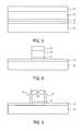
- FIG. 2illustrates the substrate of FIG. 1 , after an un-doped or lightly doped semiconductor layer is grown on the substrate.
- FIG. 3is a cross-sectional, elevation view of the substrate and the semiconductor layer of FIG. 2 , in addition to other layers used to form gates.
- FIG. 4illustrates the substrate of FIG. 3 , after the formation of gates.
- FIG. 5illustrates the substrate of FIG. 4 , after the formation of sidewall spacers on the gates.
- FIG. 6illustrates the substrate of FIG. 5 , after an etching step used to etch the semiconductor layer. This figure shows the undercutting of the gate.
- FIG. 7illustrates the substrate of FIG. 6 following the epitaxial growth of source and drain regions.
- FIG. 8illustrates the structure of FIG. 7 , after the formation of additional spacers and the doping of the exposed portion of the source and drain regions.
- FIG. 9illustrates the structure of FIG. 8 following the formation of a salicide layer.
- FIG. 10illustrates the structure of FIG. 9 where two transistors are shown side-by-side, specifically an n-channel transistor and a p-channel transistor are depicted.
- FIG. 11illustrates the structure of FIG. 10 following the chemical mechanical polishing (CMP) of an interlayer dielectric (ILD).
- CMPchemical mechanical polishing
- ILDinterlayer dielectric
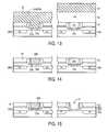
- FIG. 12illustrates the structure of FIG. 11 , after the formation of a photoresist layer over the p-channel transistor region and the removal of the polysilicon gate and its underlying insulative layer from the n-channel gate.
- FIG. 13illustrates the structure of FIG. 12 following the formation of an n-metal layer.
- FIG. 14illustrates the structure of FIG. 13 following a CMP process.
- FIG. 15illustrates the structure of FIG. 14 after the removal of the polysilicon gate and its underlying insulative layer from the p-channel gate.
- FIG. 16illustrates the structure of FIG. 15 following the deposition of a p-metal.
- FIG. 17illustrates the structure of FIG. 16 following a CMP process.
- MOScomplementary metal-oxide-semiconductor
- FIG. 1the upper approximately 200 nanometers (nm) of a monocrystalline silicon substrate 10 is illustrated. As shown, the upper region of this substrate is heavily doped with a dopant such as boron.
- the doping profileillustrates that the doping level has a peak below the surface in excess of 10 19 atoms/cm 3 , or higher. This doping profile may be achieved using ion implantation.
- a epitaxial layershown as a monocrystalline silicon layer 12 , is formed on the upper surface of the substrate 10 .
- the deposition of the epitaxial silicon layer 12is carried out using dichloro-silane based chemistry in a single wafer CVD reactor, such as ASM E3000 reactor.
- the filmis deposited with gas flows of 140-250 sccm of dicholoro silane (SiH 2 Cl 2 ), 100-150 sccm HCl, 20 slm of H 2 at 825° C. and a process pressure of 20 Torr.
- the layer 12may have the thickness of approximately 85 nm, and its doping concentration will be, for example, less than 1/100 of the buried peak doping concentration of the substrate.
- sidewalls 16are then formed on the gate of FIG. 4 .
- Relatively thin silicon nitride sidewall members 16may be formed using ordinary sidewall processing. The purpose of these sidewall spacers is to protect the polysilicon during subsequent processing. Consequently, all sides of the polysilicon gate 14 are covered. Because the sidewall spacers are used for protection of the polysilicon, they may be relatively thin.
- the layer 12is etched to form a channel body 12 a .
- the etchingundercuts the gate structure as shown by the undercuts 20 in FIG. 6 .
- the layer 12may be etched with a variety of hydroxide-based solutions. However, for high selectivity to the heavily doped substrate, relatively mild processing conditions and a wet etchant are employed.
- One methodis treatment with an aqueous ammonium hydroxide solution in the concentration range 2-10% by volume at 25 degrees Celsius with a sonication transducer which dissipates ultra- or mega-sonic energy at a power of 0.5 to 5 W/cm 2 .
- Source and drain regionsare then grown to establish a shallow, highly doped source/drain tip (extension) that laterally extends the distance under the gate edge to the channel body 12 a .
- Separate processingis used for the p-channel and n-channel transistors with each of the source and drain regions being grown in different processing steps, both with in-situ doping. This results in the source and drain regions being highly doped, in one case with a p-type dopant, and in the other case with an n-type dopant.
- the source/drain extension (tip)are raised source/drain regions formed by selectively depositing epitaxial boron (B) doped silicon or SiGe with germanium concentrations up to 30%.
- Bepitaxial boron
- the processing conditions100 sccm of dichlorosilane (DCS), 20 slm H 2 , 750-800° C., 20 Torr, 150-200 sccm HCl, a diborane (B 2 H 6 ) flow of 150-200 sccm and aGeH 4 flow of 150-200 sccm, a highly doped SiGe film with a deposition rate of 20 nm/min, B concentration of 1E20 cm ⁇ 3 and a germanium concentration of 20% is achieved.
- DCSdichlorosilane
- B 2 H 6diborane
- a low resistivity of 0.7-0.9 mOhm-cm resulting from the high B concentration in the filmprovides the benefit of high conductivity in the tip source/drain regions and thereby reduced R external .
- SiGe in the source/drain regionsexerts compressive strain on the channel, which in turn results in enhanced mobility and improved transistor performance.
- the source/drain regionsare formed using in-situ phosphorous doped silicon deposited selectively under processing conditions of 100 sccm of DCS, 25-50 sccm HCl, 200-300 sccm of 1% Ph 3 with a carrier H 2 gas flow of 20 slm at 750° C. and 20 Torr.
- a phosphorous concentration of 2E20 cm ⁇ 3 with a resistivity of 0.4-0.6 mOhm-cmis achieved in the deposited film.
- additional spacers 24are formed using ordinary processing.
- the spacersmay be a silicon nitride or silicon dioxide spacers. Spacers 24 are relatively thick when compared to the thickness of the spacer 16 as shown in FIG. 8 .
- Ion implantationnow occurs to from the source/drain regions 26 in the substrate 10 . Again, separate ion implantation processes are used for the p-type dopant and n-type dopant.
- the regions 26may be implanted to a level of 10 20 atoms/cm 3 .
- an ordinary silicide or salicide processis used to form the salicide layer 28 thereby making the upper surface of the source/drain regions more conductive.
- an n-channel transistoris depicted along side a p-channel transistor.
- the channel regionsare shown as 12 b for the n-channel transistor and 12 c for the p-channel transistor.
- the letter “b”is used below, to denote the layers and regions for the n-channel transistor, and similarly, the letter “c” is used to designate the layers and regions for the p-channel transistor.
- the structure shown in FIG. 10is the same as shown in FIG. 9 except that an ILD 30 is formed over the wafer. Any one of a plurality of dielectrics may be used for the ILD such as silicon dioxide, carbon doped silicon dioxide or other low-k dielectrics.
- CMPis used to provide a planarized surface and to remove the salicide from the top of the gates 14 b and 14 c .
- the resultant structureis illustrated in FIG. 11 .
- a photoresist layer 32is formed over the p-channel transistors, and a wet etchant is used to remove the polysilicon from the n-channel transistors.
- the underlying insulative layeris also removed, forming the opening 34 depicted in FIG. 12 .
- an insulative layer 37 bis formed along with a metal layer 38 , referred to as “n-metal” since it is the metal having the appropriate work function for the n-channel transistors.
- the gate dielectricideally has a high electric constant, such as a metal oxide dielectric, for instance, HfO 2 , ZrO or other high-k dielectrics, such as PZT or BST.
- a high-k dielectric filmcan be formed by any well-known technique such as by chemical vapor deposition (CVD).
- the gate electrode layer 38may be formed by blanket deposition of a suitable gate electrode material.
- a gate electrode materialcomprises a metal film such as tungsten, tantalum and/or nitrides and alloys thereof.
- a work function in the range of 4.0 to 4.6 eVmay be used.
- CMPis next used to planarize the surface, thereby removing the metal layer 38 , except within the region formerly occupied by the polysilicon, gate.
- the resultant gate 38 b and the underlying insulative layer 37 bare illustrated in FIG. 14 .
- a wet etchantis used to remove the polysilicon gate associated with the p-channel transistors. Again, the underlying insulative layer is also removed so that a more appropriate insulative layer may be formed.
- the opening 42 of FIG. 15results after the polysilicon gate and the underlying insulative layer are removed.
- a gate dielectric 37 cis formed on the exposed silicon. This dielectric may be the same as dielectric 37 b.
- a metal layer 44is formed over the structure of FIG. 15 and the gate dielectric 37 b . This is shown as a “p-metal” in FIG. 16 since the work function of this metal is appropriate for p-channel transistors.
- the p-metalmay be of the same composition as the n-metal except that the work function is preferable between 4.6 to 5.2 eV.
- CMPis used to planarize the structure with the resultant structure being shown in FIG. 17 .
- An n-channel transistor with a gate 37 b and a channel region 12 bresults, and similarly, a p-channel transistor with a gate 44 c and a channel region 12 c results.
- the transistors of FIG. 17there are several advantages to the transistors of FIG. 17 and their fabrication when compared to prior art transistors.
- shallow tip (extension) junction depthsare desirable to help support smaller transistor dimensions.
- minimum tip junction depthsare limited by the necessary gate overlap.
- the gate overlap dimension and the junction depthcan be better controlled. For instance, the wet etch can be timed to determine the extent of undercutting under the gate structure.
- the shallow tip junction depthsallow fabrication of shorter gate lengths without increasing off-state leakage current. Tip doping is needed under the gate edge to assure a low risistance path between the inversion layer under the gate and the highly doped source/drain tip region. The low resistance permits higher drive currents which are critical for circuit switching speed.
Landscapes
- Engineering & Computer Science (AREA)
- Microelectronics & Electronic Packaging (AREA)
- Condensed Matter Physics & Semiconductors (AREA)
- General Physics & Mathematics (AREA)
- Manufacturing & Machinery (AREA)
- Computer Hardware Design (AREA)
- Physics & Mathematics (AREA)
- Power Engineering (AREA)
- Chemical & Material Sciences (AREA)
- Chemical Kinetics & Catalysis (AREA)
- Crystallography & Structural Chemistry (AREA)
- General Chemical & Material Sciences (AREA)
- Insulated Gate Type Field-Effect Transistor (AREA)
- Metal-Oxide And Bipolar Metal-Oxide Semiconductor Integrated Circuits (AREA)
- Thin Film Transistor (AREA)
Abstract
Description
- The invention relates to the field of MOS transistors, particularly those fabricated with epitaxial source and drain regions.
- Delta-doped transistors are described in Noda et al. “0.1 μm Delta-Doped MOSFET Using Post Low Energy Implanting Selective Epitaxy,”VLSI Technology1994.Digest of Technical Papers. The motivation for the Delta-doped transistor is that higher mobility (less impurity scattering) is achieved with an un-doped or lightly doped channel. Such devices are also described in patent application Ser. No. 10/692,696, filed Oct. 24, 2003, titled “Epitaxially Deposited Source/Drain,” assigned to the assignee of the present application.
- The fabrication of these transistors relies in large part upon the difference in the doping levels between the heavily doped substrate and the lightly doped or un-doped epitaxially formed surface of the substrate. An etchant is able to discriminate between the surface region and the main body of the substrate because of this difference in doping levels. One problem that occurs, however, is that when the gate structures are formed, relatively high temperature processing is needed to, for instance, activate the doping in a polysilicon gate. This causes the diffusion of the dopant from the substrate into the channel region, thereby deteriorating the performance of the transistors.
FIG. 1 is a cross-sectional, elevation view of the upper portion of a silicon substrate used to illustrate the doping profile in the upper region of the substrate.FIG. 2 illustrates the substrate ofFIG. 1 , after an un-doped or lightly doped semiconductor layer is grown on the substrate.FIG. 3 is a cross-sectional, elevation view of the substrate and the semiconductor layer ofFIG. 2 , in addition to other layers used to form gates.FIG. 4 illustrates the substrate ofFIG. 3 , after the formation of gates.FIG. 5 illustrates the substrate ofFIG. 4 , after the formation of sidewall spacers on the gates.FIG. 6 illustrates the substrate ofFIG. 5 , after an etching step used to etch the semiconductor layer. This figure shows the undercutting of the gate.FIG. 7 illustrates the substrate ofFIG. 6 following the epitaxial growth of source and drain regions.FIG. 8 illustrates the structure ofFIG. 7 , after the formation of additional spacers and the doping of the exposed portion of the source and drain regions.FIG. 9 illustrates the structure ofFIG. 8 following the formation of a salicide layer.FIG. 10 illustrates the structure ofFIG. 9 where two transistors are shown side-by-side, specifically an n-channel transistor and a p-channel transistor are depicted.FIG. 11 illustrates the structure ofFIG. 10 following the chemical mechanical polishing (CMP) of an interlayer dielectric (ILD).FIG. 12 illustrates the structure ofFIG. 11 , after the formation of a photoresist layer over the p-channel transistor region and the removal of the polysilicon gate and its underlying insulative layer from the n-channel gate.FIG. 13 illustrates the structure ofFIG. 12 following the formation of an n-metal layer.FIG. 14 illustrates the structure ofFIG. 13 following a CMP process.FIG. 15 illustrates the structure ofFIG. 14 after the removal of the polysilicon gate and its underlying insulative layer from the p-channel gate.FIG. 16 illustrates the structure ofFIG. 15 following the deposition of a p-metal.FIG. 17 illustrates the structure ofFIG. 16 following a CMP process.- A process for fabricating complementary metal-oxide-semiconductor (MOS) field-effect transistors and the resultant transistors are described. In the following description, numerous specific details are set forth such as specific dopant concentration levels, specific chemicals, etc. in order to provide a thorough understanding of the present invention. It will be apparent to one skilled in the art that these specific details are not required to practice the present invention. In other instances, well-known processing steps, such as cleaning steps, are not described in detail in order not to unnecessarily obscure the following disclosure.
- In
FIG. 1 , the upper approximately 200 nanometers (nm) of amonocrystalline silicon substrate 10 is illustrated. As shown, the upper region of this substrate is heavily doped with a dopant such as boron. The doping profile illustrates that the doping level has a peak below the surface in excess of 1019atoms/cm3, or higher. This doping profile may be achieved using ion implantation. - Following the doping of the substrate, a epitaxial layer, shown as a
monocrystalline silicon layer 12, is formed on the upper surface of thesubstrate 10. For instance, the deposition of theepitaxial silicon layer 12 is carried out using dichloro-silane based chemistry in a single wafer CVD reactor, such as ASM E3000 reactor. The film is deposited with gas flows of 140-250 sccm of dicholoro silane (SiH2Cl2), 100-150 sccm HCl, 20 slm of H2at 825° C. and a process pressure of 20 Torr. Under these processing conditions, a deposition rate of 10-15 nm/min is achieved for silicon on the exposed substrate while achieving an excellent selectivity for spacer and oxide regions. Thelayer 12 may have the thickness of approximately 85 nm, and its doping concentration will be, for example, less than 1/100 of the buried peak doping concentration of the substrate. - Following the formation of the
layer 12, aninsulative layer 13 is formed onlayer 10.Layer 13 may be a thin, thermally grown oxide layer or a deposited silicon dioxide layer. Next, apolysilicon layer 14 is deposited on theinsulative layer 13. As will be seen, gates formed from thelayer 14 are sacrificial. They are subsequently removed and metal is substituted for the regions occupied by these polysilicon gates. Ahard mask 15 is formed on thepolysilicon layer 14. - Next, as shown in
FIG. 4 , a sacrificial gate structure is fabricated by first masking and etching thehard mask layer 15 using ordinary photolithographic processing to define masking members for gates. Now, thepolysilicon layer 14 andinsulative layer 13 are etched in alignment with thehard mask 15 using ordinary etchants. The resultant structure is depicted inFIG. 4 . - As shown in
FIG. 5 ,sidewalls 16 are then formed on the gate ofFIG. 4 . Relatively thin siliconnitride sidewall members 16 may be formed using ordinary sidewall processing. The purpose of these sidewall spacers is to protect the polysilicon during subsequent processing. Consequently, all sides of thepolysilicon gate 14 are covered. Because the sidewall spacers are used for protection of the polysilicon, they may be relatively thin. - Now, the
layer 12 is etched to form achannel body 12a. The etching undercuts the gate structure as shown by theundercuts 20 inFIG. 6 . - The
layer 12 may be etched with a variety of hydroxide-based solutions. However, for high selectivity to the heavily doped substrate, relatively mild processing conditions and a wet etchant are employed. One method is treatment with an aqueous ammonium hydroxide solution in the concentration range 2-10% by volume at 25 degrees Celsius with a sonication transducer which dissipates ultra- or mega-sonic energy at a power of 0.5 to 5 W/cm2. - Source and drain regions are then grown to establish a shallow, highly doped source/drain tip (extension) that laterally extends the distance under the gate edge to the
channel body 12a. Separate processing is used for the p-channel and n-channel transistors with each of the source and drain regions being grown in different processing steps, both with in-situ doping. This results in the source and drain regions being highly doped, in one case with a p-type dopant, and in the other case with an n-type dopant. - In forming a PMOS transistor, the source/drain extension (tip) are raised source/drain regions formed by selectively depositing epitaxial boron (B) doped silicon or SiGe with germanium concentrations up to 30%. Under the processing conditions of 100 sccm of dichlorosilane (DCS), 20 slm H2, 750-800° C., 20 Torr, 150-200 sccm HCl, a diborane (B2H6) flow of 150-200 sccm and aGeH4flow of 150-200 sccm, a highly doped SiGe film with a deposition rate of 20 nm/min, B concentration of 1E20 cm−3and a germanium concentration of 20% is achieved. A low resistivity of 0.7-0.9 mOhm-cm resulting from the high B concentration in the film provides the benefit of high conductivity in the tip source/drain regions and thereby reduced Rexternal. SiGe in the source/drain regions exerts compressive strain on the channel, which in turn results in enhanced mobility and improved transistor performance.
- For an NMOS transistor, the source/drain regions are formed using in-situ phosphorous doped silicon deposited selectively under processing conditions of 100 sccm of DCS, 25-50 sccm HCl, 200-300 sccm of 1% Ph3with a carrier H2gas flow of 20 slm at 750° C. and 20 Torr. A phosphorous concentration of 2E20 cm−3with a resistivity of 0.4-0.6 mOhm-cm is achieved in the deposited film.
- After the source/drain regions are formed as illustrated in
FIG. 7 ,additional spacers 24 are formed using ordinary processing. As an example, the spacers may be a silicon nitride or silicon dioxide spacers.Spacers 24 are relatively thick when compared to the thickness of thespacer 16 as shown inFIG. 8 . - Ion implantation now occurs to from the source/
drain regions 26 in thesubstrate 10. Again, separate ion implantation processes are used for the p-type dopant and n-type dopant. Theregions 26 may be implanted to a level of 1020atoms/cm3. - As shown in
FIG. 9 , an ordinary silicide or salicide process is used to form thesalicide layer 28 thereby making the upper surface of the source/drain regions more conductive. - In
FIG. 10 , an n-channel transistor is depicted along side a p-channel transistor. The channel regions are shown as12bfor the n-channel transistor and12cfor the p-channel transistor. The letter “b” is used below, to denote the layers and regions for the n-channel transistor, and similarly, the letter “c” is used to designate the layers and regions for the p-channel transistor. The structure shown inFIG. 10 is the same as shown inFIG. 9 except that anILD 30 is formed over the wafer. Any one of a plurality of dielectrics may be used for the ILD such as silicon dioxide, carbon doped silicon dioxide or other low-k dielectrics. - Now, CMP is used to provide a planarized surface and to remove the salicide from the top of the
gates FIG. 11 . - Next, a
photoresist layer 32 is formed over the p-channel transistors, and a wet etchant is used to remove the polysilicon from the n-channel transistors. The underlying insulative layer is also removed, forming theopening 34 depicted inFIG. 12 . - Now, as shown in
FIG. 13 , aninsulative layer 37bis formed along with ametal layer 38, referred to as “n-metal” since it is the metal having the appropriate work function for the n-channel transistors. The gate dielectric, ideally has a high electric constant, such as a metal oxide dielectric, for instance, HfO2, ZrO or other high-k dielectrics, such as PZT or BST. A high-k dielectric film can be formed by any well-known technique such as by chemical vapor deposition (CVD). Thegate electrode layer 38 may be formed by blanket deposition of a suitable gate electrode material. In one embodiment, a gate electrode material comprises a metal film such as tungsten, tantalum and/or nitrides and alloys thereof. For the n-channel transistors, a work function in the range of 4.0 to 4.6 eV may be used. - CMP is next used to planarize the surface, thereby removing the
metal layer 38, except within the region formerly occupied by the polysilicon, gate. Theresultant gate 38band theunderlying insulative layer 37bare illustrated inFIG. 14 . - A wet etchant is used to remove the polysilicon gate associated with the p-channel transistors. Again, the underlying insulative layer is also removed so that a more appropriate insulative layer may be formed. The
opening 42 ofFIG. 15 results after the polysilicon gate and the underlying insulative layer are removed. A gate dielectric37cis formed on the exposed silicon. This dielectric may be the same as dielectric37b. - A metal layer44 is formed over the structure of
FIG. 15 and thegate dielectric 37b. This is shown as a “p-metal” inFIG. 16 since the work function of this metal is appropriate for p-channel transistors. The p-metal may be of the same composition as the n-metal except that the work function is preferable between 4.6 to 5.2 eV. - After the deposition of the p-metal, CMP is used to planarize the structure with the resultant structure being shown in
FIG. 17 . An n-channel transistor with agate 37band achannel region 12bresults, and similarly, a p-channel transistor with a gate44cand achannel region 12cresults. - There are several advantages to the transistors of
FIG. 17 and their fabrication when compared to prior art transistors. First, shallow tip (extension) junction depths are desirable to help support smaller transistor dimensions. When using traditional implanted tip techniques, minimum tip junction depths are limited by the necessary gate overlap. With the structure ofFIG. 17 and the described processing, the gate overlap dimension and the junction depth can be better controlled. For instance, the wet etch can be timed to determine the extent of undercutting under the gate structure. - The shallow tip junction depths allow fabrication of shorter gate lengths without increasing off-state leakage current. Tip doping is needed under the gate edge to assure a low risistance path between the inversion layer under the gate and the highly doped source/drain tip region. The low resistance permits higher drive currents which are critical for circuit switching speed.
- An advantage of the metal gate is that the processing can occur at lower temperatures. This is in addition to the better performance achieved with the metal gate when compared to a polysilicon gate. In the processing described above, lower temperature options are used to reduce the total thermal exposure. This as mentioned earlier, prevents the dopant from the substrate from diffusing into the channel region. Thus, a delta-doped transistor with a metal gate and method of fabrication have been described.
Claims (20)
1. A semiconductor process comprising:
growing an un-doped or lightly doped silicon layer on a heavily doped substrate;
forming sacrificial polysilicon gates on the silicon layer;
etching the silicon layer and undercutting the gate structures so as to form silicon bodies under the gate structures;
growing source and drain regions which extend into the undercutting adjacent to the silicon bodies;
removing the polysilicon gates; and
forming metal gates in place of the polysilicon gates.
2. The process ofclaim 1 , wherein the processing is carried out at relatively low temperatures so as to prevent dopant from the substrate to substantially dope the silicon layer or silicon bodies.
3. The process ofclaim 1 , wherein the etching of the silicon layer is done with a wet etchant which discriminates between the silicon layer and the silicon substrate.
4. The process ofclaim 2 , wherein the source and drain regions are selectively grown regions of silicon or silicon-germanium.
5. The process ofclaim 4 , wherein the source and drain regions are heavily doped regions.
6. The process ofclaim 1 , wherein:
first source and drain regions are selectively grown and heavily doped with an n-type dopant, and
second source and drain regions are selectively grown and heavily doped with a p-type dopant.
7. The process ofclaim 6 , wherein:
first metal gates are formed above the first source and drain regions having a work function of between 4.0 to 4.6 eV; and
second metal gates are formed above the second source and drain regions having a work function of between 4.6 to 5.2 eV.
8. The process ofclaim 6 , wherein the forming of the metal gates comprises:
removing the polysilicon gates above the first source and drain regions;
depositing a first metal;
polishing away the first metal above the second source and drain regions;
removing the polysilicon gates above the second source and drain regions;
depositing a second metal;
polishing away the second metal above the first source and drain regions.
9. The process ofclaim 6 , wherein the first metal has a work function of between 4.0 to 4.6 eV, and the second metal has a work function of between 4.6 and 5.2 eV.
10. A process for forming complementary MOS transistors comprising:
forming a highly doped or un-doped monocrystalline layer on a heavily doped monocrystalline substrate;
forming polysilicon members on the layer;
etching the layer to form channel regions for the transistors, undercutting the polysilicon members;
growing first and second monocrystalline source and drain regions doped with an n-type and p-type dopant, respectively extending from opposite side of the channel regions from beneath the polysilicon members; and
replacing the polysilicon members with a first metal and a second metal for the first and second source and drain regions, respectively.
11. The process ofclaim 10 , wherein first side spacers are formed on the polysilicon members before the etching of the layer.
12. The process ofclaim 11 , wherein second side spacers are formed on the first spacers following the formation of the first and second source and drain regions.
13. The process ofclaim 12 , including doping the first and second source and drain regions and the substrate in alignment with the second spacers.
14. The process ofclaim 10 , wherein the first metal has a work function of between 4.0 to 4.6 eV, and the second metal has a work function of between 4.6 to 5.2 eV.
15. An MOS transistor comprising:
a heavily doped substrate;
an un-doped or lightly doped channel region disposed on the substrate;
raised, monocrystalline source and drain regions disposed on the substrate, extending from opposite sides of the channel region, and
a metal gate insulated from and disposed over the channel region and over at least a portion of the source and drain regions.
16. The transistor ofclaim 15 , including first sidewall spacers disposed about the metal gate.
17. The transistor ofclaim 15 , including a silicide layer on portions of the source and drain regions extending beyond the metal gate and first sidewall spacers.
18. The transistor ofclaim 15 , including source and drain diffusions extending into the substrate.
19. The transistor ofclaim 15 , wherein the source and drain regions comprise silicon or silicon-germanium.
20. The transistor ofclaim 15 , wherein the substrate has a peak doping concentration of 1019atoms/cm3or greater.
Priority Applications (11)
| Application Number | Priority Date | Filing Date | Title |
|---|---|---|---|
| US10/955,669US7332439B2 (en) | 2004-09-29 | 2004-09-29 | Metal gate transistors with epitaxial source and drain regions |
| CN201310419494.2ACN103560150B (en) | 2004-09-29 | 2005-09-29 | Metal gate transistors with epitaxial source and drain regions |
| US11/240,440US7915167B2 (en) | 2004-09-29 | 2005-09-29 | Fabrication of channel wraparound gate structure for field-effect transistor |
| PCT/US2005/035377WO2006039597A2 (en) | 2004-09-29 | 2005-09-29 | Metal gate transistors with epitaxial source and drain regions |
| KR1020077007071AKR100867781B1 (en) | 2004-09-29 | 2005-09-29 | Metal gate transistors with epitaxial source and drain regions |
| TW094133997ATWI272681B (en) | 2004-09-29 | 2005-09-29 | Metal gate transistors with epitaxial source and drain regions |
| CNA2005800324531ACN101027763A (en) | 2004-09-29 | 2005-09-29 | Metal Gate Transistor with Epitaxial Source and Drain Regions |
| DE112005002302TDE112005002302B4 (en) | 2004-09-29 | 2005-09-29 | Method for producing metal gate transistors with epitaxial source and drain regions and MOS transistor |
| US12/011,439US8344452B2 (en) | 2004-09-29 | 2008-01-24 | Metal gate transistors with raised source and drain regions formed on heavily doped substrate |
| US13/042,973US20110156145A1 (en) | 2004-09-29 | 2011-03-08 | Fabrication of channel wraparound gate structure for field-effect transistor |
| US15/197,563US20160308014A1 (en) | 2004-09-29 | 2016-06-29 | Fabrication of channel wraparound gate structure for field-effect transistor |
Applications Claiming Priority (1)
| Application Number | Priority Date | Filing Date | Title |
|---|---|---|---|
| US10/955,669US7332439B2 (en) | 2004-09-29 | 2004-09-29 | Metal gate transistors with epitaxial source and drain regions |
Related Child Applications (2)
| Application Number | Title | Priority Date | Filing Date |
|---|---|---|---|
| US11/240,440ContinuationUS7915167B2 (en) | 2004-09-29 | 2005-09-29 | Fabrication of channel wraparound gate structure for field-effect transistor |
| US12/011,439DivisionUS8344452B2 (en) | 2004-09-29 | 2008-01-24 | Metal gate transistors with raised source and drain regions formed on heavily doped substrate |
Publications (2)
| Publication Number | Publication Date |
|---|---|
| US20060068590A1true US20060068590A1 (en) | 2006-03-30 |
| US7332439B2 US7332439B2 (en) | 2008-02-19 |
Family
ID=35788956
Family Applications (5)
| Application Number | Title | Priority Date | Filing Date |
|---|---|---|---|
| US10/955,669Active2025-12-18US7332439B2 (en) | 2004-09-29 | 2004-09-29 | Metal gate transistors with epitaxial source and drain regions |
| US11/240,440Expired - Fee RelatedUS7915167B2 (en) | 2004-09-29 | 2005-09-29 | Fabrication of channel wraparound gate structure for field-effect transistor |
| US12/011,439Expired - Fee RelatedUS8344452B2 (en) | 2004-09-29 | 2008-01-24 | Metal gate transistors with raised source and drain regions formed on heavily doped substrate |
| US13/042,973AbandonedUS20110156145A1 (en) | 2004-09-29 | 2011-03-08 | Fabrication of channel wraparound gate structure for field-effect transistor |
| US15/197,563AbandonedUS20160308014A1 (en) | 2004-09-29 | 2016-06-29 | Fabrication of channel wraparound gate structure for field-effect transistor |
Family Applications After (4)
| Application Number | Title | Priority Date | Filing Date |
|---|---|---|---|
| US11/240,440Expired - Fee RelatedUS7915167B2 (en) | 2004-09-29 | 2005-09-29 | Fabrication of channel wraparound gate structure for field-effect transistor |
| US12/011,439Expired - Fee RelatedUS8344452B2 (en) | 2004-09-29 | 2008-01-24 | Metal gate transistors with raised source and drain regions formed on heavily doped substrate |
| US13/042,973AbandonedUS20110156145A1 (en) | 2004-09-29 | 2011-03-08 | Fabrication of channel wraparound gate structure for field-effect transistor |
| US15/197,563AbandonedUS20160308014A1 (en) | 2004-09-29 | 2016-06-29 | Fabrication of channel wraparound gate structure for field-effect transistor |
Country Status (6)
| Country | Link |
|---|---|
| US (5) | US7332439B2 (en) |
| KR (1) | KR100867781B1 (en) |
| CN (2) | CN101027763A (en) |
| DE (1) | DE112005002302B4 (en) |
| TW (1) | TWI272681B (en) |
| WO (1) | WO2006039597A2 (en) |
Cited By (25)
| Publication number | Priority date | Publication date | Assignee | Title |
|---|---|---|---|---|
| US20060286755A1 (en)* | 2005-06-15 | 2006-12-21 | Brask Justin K | Method for fabricating transistor with thinned channel |
| US20070090408A1 (en)* | 2005-09-29 | 2007-04-26 | Amlan Majumdar | Narrow-body multiple-gate FET with dominant body transistor for high performance |
| US20070138559A1 (en)* | 2005-12-16 | 2007-06-21 | Intel Corporation | Replacement gates to enhance transistor strain |
| US20070231984A1 (en)* | 2006-03-31 | 2007-10-04 | Metz Matthew V | Uniform silicide metal on epitaxially grown source and drain regions of three-dimensional transistors |
| US20070238273A1 (en)* | 2006-03-31 | 2007-10-11 | Doyle Brian S | Method of ion implanting for tri-gate devices |
| US20080188041A1 (en)* | 2005-08-17 | 2008-08-07 | Suman Datta | Lateral undercut of metal gate in SOI device |
| US20090149012A1 (en)* | 2004-09-30 | 2009-06-11 | Brask Justin K | Method of forming a nonplanar transistor with sidewall spacers |
| US20100297838A1 (en)* | 2004-09-29 | 2010-11-25 | Chang Peter L D | Independently accessed double-gate and tri-gate transistors in same process flow |
| US20110062512A1 (en)* | 2004-10-25 | 2011-03-17 | Uday Shah | Nonplanar device with thinned lower body portion and method of fabrication |
| US7960794B2 (en) | 2004-08-10 | 2011-06-14 | Intel Corporation | Non-planar pMOS structure with a strained channel region and an integrated strained CMOS flow |
| DE112006003576B4 (en)* | 2005-12-29 | 2011-06-16 | Intel Corporation, Santa Clara | A method of forming a FET having structure for reducing the external resistance of the three-dimensional transistor by using epitaxial layers and transistor |
| US8084818B2 (en) | 2004-06-30 | 2011-12-27 | Intel Corporation | High mobility tri-gate devices and methods of fabrication |
| US8183646B2 (en) | 2005-02-23 | 2012-05-22 | Intel Corporation | Field effect transistor with narrow bandgap source and drain regions and method of fabrication |
| US20130020613A1 (en)* | 2011-07-19 | 2013-01-24 | Semiconductor Manufacturing International (Beijing) Corporation | Semiconductor device and manufacturing method thereof |
| US8362566B2 (en) | 2008-06-23 | 2013-01-29 | Intel Corporation | Stress in trigate devices using complimentary gate fill materials |
| US8405164B2 (en) | 2003-06-27 | 2013-03-26 | Intel Corporation | Tri-gate transistor device with stress incorporation layer and method of fabrication |
| EP2608264A1 (en)* | 2011-12-23 | 2013-06-26 | Imec | Method for manufacturing a field-effect semiconductor device following a replacement gate process |
| US20140004677A1 (en)* | 2012-06-29 | 2014-01-02 | GlobalFoundries, Inc. | High-k Seal for Protection of Replacement Gates |
| TWI466293B (en)* | 2008-08-28 | 2014-12-21 | Taiwan Semiconductor Mfg Co Ltd | Integrated circuit with metal gate stack and forming method thereof |
| US9059209B2 (en) | 2011-08-01 | 2015-06-16 | International Business Machines Corporation | Replacement gate ETSOI with sharp junction |
| US9263566B2 (en) | 2011-07-19 | 2016-02-16 | Semiconductor Manufacturing International (Beijing) Corporation | Semiconductor device and manufacturing method thereof |
| US9385180B2 (en) | 2005-06-21 | 2016-07-05 | Intel Corporation | Semiconductor device structures and methods of forming semiconductor structures |
| US9502529B2 (en) | 2006-12-11 | 2016-11-22 | Sony Corporation | Metal oxide semiconductor having epitaxial source drain regions and a method of manufacturing same using dummy gate process |
| US11373867B2 (en)* | 2010-11-18 | 2022-06-28 | Taiwan Semiconductor Manufacturing Company, Ltd. | Integrated circuits having source/drain structure and method of making |
| WO2023140840A1 (en)* | 2022-01-20 | 2023-07-27 | Applied Materials, Inc. | Methods for near surface work function engineering |
Families Citing this family (109)
| Publication number | Priority date | Publication date | Assignee | Title |
|---|---|---|---|---|
| AU2002306436A1 (en)* | 2001-02-12 | 2002-10-15 | Asm America, Inc. | Improved process for deposition of semiconductor films |
| US7456476B2 (en) | 2003-06-27 | 2008-11-25 | Intel Corporation | Nonplanar semiconductor device with partially or fully wrapped around gate electrode and methods of fabrication |
| US7268058B2 (en)* | 2004-01-16 | 2007-09-11 | Intel Corporation | Tri-gate transistors and methods to fabricate same |
| US7154118B2 (en)* | 2004-03-31 | 2006-12-26 | Intel Corporation | Bulk non-planar transistor having strained enhanced mobility and methods of fabrication |
| KR20070006852A (en)* | 2004-04-23 | 2007-01-11 | 에이에스엠 아메리카, 인코포레이티드 | In-situ doped epitaxial film |
| US7611943B2 (en)* | 2004-10-20 | 2009-11-03 | Texas Instruments Incorporated | Transistors, integrated circuits, systems, and processes of manufacture with improved work function modulation |
| JP4369359B2 (en) | 2004-12-28 | 2009-11-18 | 富士通マイクロエレクトロニクス株式会社 | Semiconductor device |
| US7816236B2 (en)* | 2005-02-04 | 2010-10-19 | Asm America Inc. | Selective deposition of silicon-containing films |
| US20060202266A1 (en)* | 2005-03-14 | 2006-09-14 | Marko Radosavljevic | Field effect transistor with metal source/drain regions |
| US7279375B2 (en)* | 2005-06-30 | 2007-10-09 | Intel Corporation | Block contact architectures for nanoscale channel transistors |
| US20070090416A1 (en) | 2005-09-28 | 2007-04-26 | Doyle Brian S | CMOS devices with a single work function gate electrode and method of fabrication |
| US7485503B2 (en) | 2005-11-30 | 2009-02-03 | Intel Corporation | Dielectric interface for group III-V semiconductor device |
| WO2007078802A2 (en)* | 2005-12-22 | 2007-07-12 | Asm America, Inc. | Epitaxial deposition of doped semiconductor materials |
| US7422960B2 (en) | 2006-05-17 | 2008-09-09 | Micron Technology, Inc. | Method of forming gate arrays on a partial SOI substrate |
| US8143646B2 (en) | 2006-08-02 | 2012-03-27 | Intel Corporation | Stacking fault and twin blocking barrier for integrating III-V on Si |
| US7537994B2 (en) | 2006-08-28 | 2009-05-26 | Micron Technology, Inc. | Methods of forming semiconductor devices, assemblies and constructions |
| US20080054361A1 (en)* | 2006-08-30 | 2008-03-06 | Infineon Technologies Ag | Method and apparatus for reducing flicker noise in a semiconductor device |
| US7999251B2 (en)* | 2006-09-11 | 2011-08-16 | International Business Machines Corporation | Nanowire MOSFET with doped epitaxial contacts for source and drain |
| US7786518B2 (en)* | 2007-12-27 | 2010-08-31 | Texas Instruments Incorporated | Growth of unfaceted SiGe in MOS transistor fabrication |
| US20090170270A1 (en)* | 2007-12-27 | 2009-07-02 | Texas Instruments Incorporated | Integration schemes to avoid faceted sige |
| US20110079861A1 (en)* | 2009-09-30 | 2011-04-07 | Lucian Shifren | Advanced Transistors with Threshold Voltage Set Dopant Structures |
| US8273617B2 (en) | 2009-09-30 | 2012-09-25 | Suvolta, Inc. | Electronic devices and systems, and methods for making and using the same |
| US8421162B2 (en) | 2009-09-30 | 2013-04-16 | Suvolta, Inc. | Advanced transistors with punch through suppression |
| US8367528B2 (en)* | 2009-11-17 | 2013-02-05 | Asm America, Inc. | Cyclical epitaxial deposition and etch |
| KR101634748B1 (en) | 2009-12-08 | 2016-07-11 | 삼성전자주식회사 | method for manufacturing MOS transistor and forming method of integrated circuit using the sime |
| US8399314B2 (en)* | 2010-03-25 | 2013-03-19 | International Business Machines Corporation | p-FET with a strained nanowire channel and embedded SiGe source and drain stressors |
| US8530286B2 (en) | 2010-04-12 | 2013-09-10 | Suvolta, Inc. | Low power semiconductor transistor structure and method of fabrication thereof |
| CN102222692B (en)* | 2010-04-14 | 2013-06-12 | 中国科学院微电子研究所 | Semiconductor device and method for manufacturing the same |
| US8569128B2 (en) | 2010-06-21 | 2013-10-29 | Suvolta, Inc. | Semiconductor structure and method of fabrication thereof with mixed metal types |
| US8759872B2 (en) | 2010-06-22 | 2014-06-24 | Suvolta, Inc. | Transistor with threshold voltage set notch and method of fabrication thereof |
| CN102376572A (en)* | 2010-08-10 | 2012-03-14 | 中芯国际集成电路制造(上海)有限公司 | Method for producing semiconductor device |
| US8377783B2 (en) | 2010-09-30 | 2013-02-19 | Suvolta, Inc. | Method for reducing punch-through in a transistor device |
| US11469271B2 (en)* | 2010-10-11 | 2022-10-11 | Monolithic 3D Inc. | Method to produce 3D semiconductor devices and structures with memory |
| US11508605B2 (en)* | 2010-11-18 | 2022-11-22 | Monolithic 3D Inc. | 3D semiconductor memory device and structure |
| US8404551B2 (en) | 2010-12-03 | 2013-03-26 | Suvolta, Inc. | Source/drain extension control for advanced transistors |
| DE102011004322B4 (en)* | 2011-02-17 | 2012-12-06 | Globalfoundries Dresden Module One Llc & Co. Kg | A method of manufacturing a semiconductor device having self-aligned contact elements and an exchange gate electrode structure |
| US8461875B1 (en) | 2011-02-18 | 2013-06-11 | Suvolta, Inc. | Digital circuits having improved transistors, and methods therefor |
| US8574990B2 (en) | 2011-02-24 | 2013-11-05 | United Microelectronics Corp. | Method of manufacturing semiconductor device having metal gate |
| US8525271B2 (en) | 2011-03-03 | 2013-09-03 | Suvolta, Inc. | Semiconductor structure with improved channel stack and method for fabrication thereof |
| US8802524B2 (en) | 2011-03-22 | 2014-08-12 | United Microelectronics Corp. | Method of manufacturing semiconductor device having metal gates |
| US8400219B2 (en) | 2011-03-24 | 2013-03-19 | Suvolta, Inc. | Analog circuits having improved transistors, and methods therefor |
| US8748270B1 (en) | 2011-03-30 | 2014-06-10 | Suvolta, Inc. | Process for manufacturing an improved analog transistor |
| US8835266B2 (en) | 2011-04-13 | 2014-09-16 | International Business Machines Corporation | Method and structure for compound semiconductor contact |
| US8796048B1 (en) | 2011-05-11 | 2014-08-05 | Suvolta, Inc. | Monitoring and measurement of thin film layers |
| US8999861B1 (en) | 2011-05-11 | 2015-04-07 | Suvolta, Inc. | Semiconductor structure with substitutional boron and method for fabrication thereof |
| US8811068B1 (en) | 2011-05-13 | 2014-08-19 | Suvolta, Inc. | Integrated circuit devices and methods |
| US8569156B1 (en) | 2011-05-16 | 2013-10-29 | Suvolta, Inc. | Reducing or eliminating pre-amorphization in transistor manufacture |
| US8735987B1 (en) | 2011-06-06 | 2014-05-27 | Suvolta, Inc. | CMOS gate stack structures and processes |
| US8995204B2 (en) | 2011-06-23 | 2015-03-31 | Suvolta, Inc. | Circuit devices and methods having adjustable transistor body bias |
| CN102891175B (en)* | 2011-07-19 | 2016-03-16 | 中芯国际集成电路制造(北京)有限公司 | Semiconductor device and manufacture method thereof |
| CN102891177B (en)* | 2011-07-19 | 2016-03-02 | 中芯国际集成电路制造(北京)有限公司 | Semiconductor device and manufacture method thereof |
| US8629016B1 (en) | 2011-07-26 | 2014-01-14 | Suvolta, Inc. | Multiple transistor types formed in a common epitaxial layer by differential out-diffusion from a doped underlayer |
| KR101891373B1 (en) | 2011-08-05 | 2018-08-24 | 엠아이이 후지쯔 세미컨덕터 리미티드 | Semiconductor devices having fin structures and fabrication methods thereof |
| US8748986B1 (en) | 2011-08-05 | 2014-06-10 | Suvolta, Inc. | Electronic device with controlled threshold voltage |
| US8645878B1 (en) | 2011-08-23 | 2014-02-04 | Suvolta, Inc. | Porting a circuit design from a first semiconductor process to a second semiconductor process |
| US8614128B1 (en) | 2011-08-23 | 2013-12-24 | Suvolta, Inc. | CMOS structures and processes based on selective thinning |
| US8713511B1 (en) | 2011-09-16 | 2014-04-29 | Suvolta, Inc. | Tools and methods for yield-aware semiconductor manufacturing process target generation |
| US9236466B1 (en) | 2011-10-07 | 2016-01-12 | Mie Fujitsu Semiconductor Limited | Analog circuits having improved insulated gate transistors, and methods therefor |
| US9847225B2 (en)* | 2011-11-15 | 2017-12-19 | Taiwan Semiconductor Manufacturing Company, Ltd. | Semiconductor device and method of manufacturing the same |
| US8895327B1 (en) | 2011-12-09 | 2014-11-25 | Suvolta, Inc. | Tipless transistors, short-tip transistors, and methods and circuits therefor |
| US8819603B1 (en) | 2011-12-15 | 2014-08-26 | Suvolta, Inc. | Memory circuits and methods of making and designing the same |
| KR101700213B1 (en) | 2011-12-21 | 2017-01-26 | 인텔 코포레이션 | Methods for forming fins for metal oxide semiconductor device structures |
| US8883600B1 (en) | 2011-12-22 | 2014-11-11 | Suvolta, Inc. | Transistor having reduced junction leakage and methods of forming thereof |
| US8599623B1 (en) | 2011-12-23 | 2013-12-03 | Suvolta, Inc. | Circuits and methods for measuring circuit elements in an integrated circuit device |
| CN103187290B (en)* | 2011-12-31 | 2015-10-21 | 中芯国际集成电路制造(北京)有限公司 | Fin type field-effect transistor and manufacture method thereof |
| US8735258B2 (en)* | 2012-01-05 | 2014-05-27 | Taiwan Semiconductor Manufacturing Company, Ltd. | Integrated circuit resistor fabrication with dummy gate removal |
| US8970289B1 (en) | 2012-01-23 | 2015-03-03 | Suvolta, Inc. | Circuits and devices for generating bi-directional body bias voltages, and methods therefor |
| US8877619B1 (en) | 2012-01-23 | 2014-11-04 | Suvolta, Inc. | Process for manufacture of integrated circuits with different channel doping transistor architectures and devices therefrom |
| US9093550B1 (en) | 2012-01-31 | 2015-07-28 | Mie Fujitsu Semiconductor Limited | Integrated circuits having a plurality of high-K metal gate FETs with various combinations of channel foundation structure and gate stack structure and methods of making same |
| US9406567B1 (en) | 2012-02-28 | 2016-08-02 | Mie Fujitsu Semiconductor Limited | Method for fabricating multiple transistor devices on a substrate with varying threshold voltages |
| US8863064B1 (en) | 2012-03-23 | 2014-10-14 | Suvolta, Inc. | SRAM cell layout structure and devices therefrom |
| US9299698B2 (en) | 2012-06-27 | 2016-03-29 | Mie Fujitsu Semiconductor Limited | Semiconductor structure with multiple transistors having various threshold voltages |
| CN103578987B (en) | 2012-07-19 | 2016-08-24 | 中国科学院微电子研究所 | Semiconductor device and method for manufacturing the same |
| US8637955B1 (en) | 2012-08-31 | 2014-01-28 | Suvolta, Inc. | Semiconductor structure with reduced junction leakage and method of fabrication thereof |
| US9112057B1 (en) | 2012-09-18 | 2015-08-18 | Mie Fujitsu Semiconductor Limited | Semiconductor devices with dopant migration suppression and method of fabrication thereof |
| US9041126B2 (en) | 2012-09-21 | 2015-05-26 | Mie Fujitsu Semiconductor Limited | Deeply depleted MOS transistors having a screening layer and methods thereof |
| US9431068B2 (en) | 2012-10-31 | 2016-08-30 | Mie Fujitsu Semiconductor Limited | Dynamic random access memory (DRAM) with low variation transistor peripheral circuits |
| US8816754B1 (en) | 2012-11-02 | 2014-08-26 | Suvolta, Inc. | Body bias circuits and methods |
| US9093997B1 (en) | 2012-11-15 | 2015-07-28 | Mie Fujitsu Semiconductor Limited | Slew based process and bias monitors and related methods |
| US9070477B1 (en) | 2012-12-12 | 2015-06-30 | Mie Fujitsu Semiconductor Limited | Bit interleaved low voltage static random access memory (SRAM) and related methods |
| US9112484B1 (en) | 2012-12-20 | 2015-08-18 | Mie Fujitsu Semiconductor Limited | Integrated circuit process and bias monitors and related methods |
| US9268885B1 (en) | 2013-02-28 | 2016-02-23 | Mie Fujitsu Semiconductor Limited | Integrated circuit device methods and models with predicted device metric variations |
| US8994415B1 (en) | 2013-03-01 | 2015-03-31 | Suvolta, Inc. | Multiple VDD clock buffer |
| US8988153B1 (en) | 2013-03-09 | 2015-03-24 | Suvolta, Inc. | Ring oscillator with NMOS or PMOS variation insensitivity |
| US9299801B1 (en) | 2013-03-14 | 2016-03-29 | Mie Fujitsu Semiconductor Limited | Method for fabricating a transistor device with a tuned dopant profile |
| US9449967B1 (en) | 2013-03-15 | 2016-09-20 | Fujitsu Semiconductor Limited | Transistor array structure |
| US9112495B1 (en) | 2013-03-15 | 2015-08-18 | Mie Fujitsu Semiconductor Limited | Integrated circuit device body bias circuits and methods |
| US9478571B1 (en) | 2013-05-24 | 2016-10-25 | Mie Fujitsu Semiconductor Limited | Buried channel deeply depleted channel transistor |
| US9412842B2 (en) | 2013-07-03 | 2016-08-09 | Samsung Electronics Co., Ltd. | Method for fabricating semiconductor device |
| US9263455B2 (en) | 2013-07-23 | 2016-02-16 | Micron Technology, Inc. | Methods of forming an array of conductive lines and methods of forming an array of recessed access gate lines |
| US8976575B1 (en) | 2013-08-29 | 2015-03-10 | Suvolta, Inc. | SRAM performance monitor |
| US9543410B2 (en)* | 2014-02-14 | 2017-01-10 | Taiwan Semiconductor Manufacturing Company Limited | Semiconductor device and formation thereof |
| US9112032B1 (en)* | 2014-06-16 | 2015-08-18 | Globalfoundries Inc. | Methods of forming replacement gate structures on semiconductor devices |
| US9710006B2 (en) | 2014-07-25 | 2017-07-18 | Mie Fujitsu Semiconductor Limited | Power up body bias circuits and methods |
| US9319013B2 (en) | 2014-08-19 | 2016-04-19 | Mie Fujitsu Semiconductor Limited | Operational amplifier input offset correction with transistor threshold voltage adjustment |
| JP6631950B2 (en)* | 2014-12-11 | 2020-01-15 | パナソニックIpマネジメント株式会社 | Nitride semiconductor device and method of manufacturing nitride semiconductor device |
| US9496338B2 (en) | 2015-03-17 | 2016-11-15 | International Business Machines Corporation | Wire-last gate-all-around nanowire FET |
| TWI695513B (en)* | 2015-03-27 | 2020-06-01 | 日商半導體能源研究所股份有限公司 | Semiconductor device and electronic device |
| KR102290685B1 (en) | 2015-06-04 | 2021-08-17 | 삼성전자주식회사 | Semiconductor device |
| JP6903446B2 (en)* | 2016-03-07 | 2021-07-14 | 芝浦メカトロニクス株式会社 | Substrate processing equipment and substrate processing method |
| US9972513B2 (en)* | 2016-03-07 | 2018-05-15 | Shibaura Mechatronics Corporation | Device and method for treating a substrate with hydrofluoric and nitric acid |
| US9768278B1 (en)* | 2016-09-06 | 2017-09-19 | Taiwan Semiconductor Manufacturing Company, Ltd. | Reduction of Fin loss in the formation of FinFETS |
| US11127590B2 (en)* | 2016-12-05 | 2021-09-21 | The Regents Of The University Of California | Method for ALD deposition on inert surfaces via Al2O3 nanoparticles |
| DE102017126544B4 (en) | 2017-06-30 | 2023-09-07 | Taiwan Semiconductor Manufacturing Co., Ltd. | PROCESSES FOR MANUFACTURING SEMICONDUCTOR DEVICES |
| US10714598B2 (en)* | 2017-06-30 | 2020-07-14 | Taiwan Semiconductor Manufacturing Co., Ltd. | Method of manufacturing semiconductor device |
| CN108231594B (en)* | 2017-12-21 | 2020-10-02 | 上海集成电路研发中心有限公司 | A kind of manufacturing method of FinFET device |
| JP2021192396A (en)* | 2018-09-14 | 2021-12-16 | キオクシア株式会社 | Integrated circuit device and manufacturing method for integrated circuit device |
| US11165032B2 (en)* | 2019-09-05 | 2021-11-02 | Taiwan Semiconductor Manufacturing Co., Ltd. | Field effect transistor using carbon nanotubes |
| CN110767804B (en)* | 2019-11-19 | 2020-11-06 | 北京元芯碳基集成电路研究院 | Carbon nanotube device and manufacturing method thereof |
Citations (9)
| Publication number | Priority date | Publication date | Assignee | Title |
|---|---|---|---|---|
| US4198250A (en)* | 1979-02-05 | 1980-04-15 | Intel Corporation | Shadow masking process for forming source and drain regions for field-effect transistors and like regions |
| US6214679B1 (en)* | 1999-12-30 | 2001-04-10 | Intel Corporation | Cobalt salicidation method on a silicon germanium film |
| US20030011037A1 (en)* | 2001-06-29 | 2003-01-16 | Chau Robert S. | Novel transistor structure and method of fabrication |
| US6524920B1 (en)* | 2001-02-09 | 2003-02-25 | Advanced Micro Devices, Inc. | Low temperature process for a transistor with elevated source and drain |
| US20030107088A1 (en)* | 1997-06-30 | 2003-06-12 | Kabushiki Kaisha Toshiba | Semiconductor device and manufacturing method therefor |
| US6777761B2 (en)* | 2002-08-06 | 2004-08-17 | International Business Machines Corporation | Semiconductor chip using both polysilicon and metal gate devices |
| US20050087801A1 (en)* | 2003-10-24 | 2005-04-28 | Nick Lindert | Epitaxially deposited source/drain |
| US7078284B2 (en)* | 2002-06-20 | 2006-07-18 | Micron Technology, Inc. | Method for forming a notched gate |
| US7084025B2 (en)* | 2004-07-07 | 2006-08-01 | Chartered Semiconductor Manufacturing Ltd | Selective oxide trimming to improve metal T-gate transistor |
Family Cites Families (285)
| Publication number | Priority date | Publication date | Assignee | Title |
|---|---|---|---|---|
| JPS58201363A (en)* | 1982-05-20 | 1983-11-24 | Sanyo Electric Co Ltd | Formation of gate electrode |
| GB2156149A (en) | 1984-03-14 | 1985-10-02 | Philips Electronic Associated | Dielectrically-isolated integrated circuit manufacture |
| US4487652A (en) | 1984-03-30 | 1984-12-11 | Motorola, Inc. | Slope etch of polyimide |
| US5514885A (en) | 1986-10-09 | 1996-05-07 | Myrick; James J. | SOI methods and apparatus |
| US4818715A (en) | 1987-07-09 | 1989-04-04 | Industrial Technology Research Institute | Method of fabricating a LDDFET with self-aligned silicide |
| US4907048A (en) | 1987-11-23 | 1990-03-06 | Xerox Corporation | Double implanted LDD transistor self-aligned with gate |
| US4905063A (en)* | 1988-06-21 | 1990-02-27 | American Telephone And Telegraph Company, At&T Bell Laboratories | Floating gate memories |
| JPH0214578A (en) | 1988-07-01 | 1990-01-18 | Fujitsu Ltd | semiconductor equipment |
| US4994873A (en) | 1988-10-17 | 1991-02-19 | Motorola, Inc. | Local interconnect for stacked polysilicon device |
| US5346834A (en) | 1988-11-21 | 1994-09-13 | Hitachi, Ltd. | Method for manufacturing a semiconductor device and a semiconductor memory device |
| US4906589A (en) | 1989-02-06 | 1990-03-06 | Industrial Technology Research Institute | Inverse-T LDDFET with self-aligned silicide |
| KR930003790B1 (en) | 1990-07-02 | 1993-05-10 | 삼성전자 주식회사 | Dielectrics for Capacitors in Semiconductor Devices |
| US5278102A (en)* | 1990-08-18 | 1994-01-11 | Fujitsu Limited | SOI device and a fabrication process thereof |
| JP3061406B2 (en) | 1990-09-28 | 2000-07-10 | 株式会社東芝 | Semiconductor device |
| JP3202223B2 (en) | 1990-11-27 | 2001-08-27 | 日本電気株式会社 | Method for manufacturing transistor |
| US5521859A (en) | 1991-03-20 | 1996-05-28 | Fujitsu Limited | Semiconductor memory device having thin film transistor and method of producing the same |
| JPH05152293A (en) | 1991-04-30 | 1993-06-18 | Sgs Thomson Microelectron Inc | Method for manufacturing stepped wall interconnect and gate |
| US5292670A (en) | 1991-06-10 | 1994-03-08 | Texas Instruments Incorporated | Sidewall doping technique for SOI transistors |
| US5179037A (en) | 1991-12-24 | 1993-01-12 | Texas Instruments Incorporated | Integration of lateral and vertical quantum well transistors in the same epitaxial stack |
| US5391506A (en) | 1992-01-31 | 1995-02-21 | Kawasaki Steel Corporation | Manufacturing method for semiconductor devices with source/drain formed in substrate projection. |
| JPH05243572A (en) | 1992-02-27 | 1993-09-21 | Fujitsu Ltd | Semiconductor device |
| US5405454A (en) | 1992-03-19 | 1995-04-11 | Matsushita Electric Industrial Co., Ltd. | Electrically insulated silicon structure and producing method therefor |
| JP2572003B2 (en) | 1992-03-30 | 1997-01-16 | 三星電子株式会社 | Method of manufacturing thin film transistor having three-dimensional multi-channel structure |
| JPH0793441B2 (en) | 1992-04-24 | 1995-10-09 | ヒュンダイ エレクトロニクス インダストリーズ カンパニー リミテッド | Thin film transistor and manufacturing method thereof |
| KR960002088B1 (en) | 1993-02-17 | 1996-02-10 | 삼성전자주식회사 | Method of manufacturing a semiconductor device having a silicon on insulator (SOI) structure |
| JPH06310547A (en) | 1993-02-25 | 1994-11-04 | Mitsubishi Electric Corp | Semiconductor device and manufacture thereof |
| EP0623963A1 (en) | 1993-05-06 | 1994-11-09 | Siemens Aktiengesellschaft | MOSFET on SOI substrate |
| US5739544A (en) | 1993-05-26 | 1998-04-14 | Matsushita Electric Industrial Co., Ltd. | Quantization functional device utilizing a resonance tunneling effect and method for producing the same |
| US6730549B1 (en) | 1993-06-25 | 2004-05-04 | Semiconductor Energy Laboratory Co., Ltd. | Semiconductor device and method for its preparation |
| JPH0750410A (en)* | 1993-08-06 | 1995-02-21 | Hitachi Ltd | Semiconductor crystal laminated body, method for forming the same, and semiconductor device |
| JP3460863B2 (en) | 1993-09-17 | 2003-10-27 | 三菱電機株式会社 | Method for manufacturing semiconductor device |
| US5883564A (en)* | 1994-04-18 | 1999-03-16 | General Motors Corporation | Magnetic field sensor having high mobility thin indium antimonide active layer on thin aluminum indium antimonide buffer layer |
| JP3317582B2 (en)* | 1994-06-01 | 2002-08-26 | 菱電セミコンダクタシステムエンジニアリング株式会社 | Method of forming fine pattern |
| JP3361922B2 (en) | 1994-09-13 | 2003-01-07 | 株式会社東芝 | Semiconductor device |
| JP3378414B2 (en) | 1994-09-14 | 2003-02-17 | 株式会社東芝 | Semiconductor device |
| US5602049A (en) | 1994-10-04 | 1997-02-11 | United Microelectronics Corporation | Method of fabricating a buried structure SRAM cell |
| JPH08125152A (en) | 1994-10-28 | 1996-05-17 | Canon Inc | Semiconductor device, correlation calculation device using the same, AD converter, DA converter, signal processing system |
| US5728594A (en)* | 1994-11-02 | 1998-03-17 | Texas Instruments Incorporated | Method of making a multiple transistor integrated circuit with thick copper interconnect |
| GB2295488B (en) | 1994-11-24 | 1996-11-20 | Toshiba Cambridge Res Center | Semiconductor device |
| US5716879A (en) | 1994-12-15 | 1998-02-10 | Goldstar Electron Company, Ltd. | Method of making a thin film transistor |
| US5710450A (en)* | 1994-12-23 | 1998-01-20 | Intel Corporation | Transistor with ultra shallow tip and method of fabrication |
| JPH08204191A (en) | 1995-01-20 | 1996-08-09 | Sony Corp | Field effect transistor and method of manufacturing the same |
| JP3303601B2 (en) | 1995-05-19 | 2002-07-22 | 日産自動車株式会社 | Groove type semiconductor device |
| KR0165398B1 (en) | 1995-05-26 | 1998-12-15 | 윤종용 | Vertical transistor manufacturing method |
| US5627097A (en)* | 1995-07-03 | 1997-05-06 | Motorola, Inc. | Method for making CMOS device having reduced parasitic capacitance |
| US5658806A (en) | 1995-10-26 | 1997-08-19 | National Science Council | Method for fabricating thin-film transistor with bottom-gate or dual-gate configuration |
| US5814895A (en) | 1995-12-22 | 1998-09-29 | Sony Corporation | Static random access memory having transistor elements formed on side walls of a trench in a semiconductor substrate |
| KR100205442B1 (en) | 1995-12-26 | 1999-07-01 | 구본준 | Thin film transistor and its manufacturing method |
| US5595919A (en)* | 1996-02-20 | 1997-01-21 | Chartered Semiconductor Manufacturing Pte Ltd. | Method of making self-aligned halo process for reducing junction capacitance |
| JPH09293793A (en) | 1996-04-26 | 1997-11-11 | Mitsubishi Electric Corp | Semiconductor device having thin film transistor and manufacturing method thereof |
| JP3710880B2 (en) | 1996-06-28 | 2005-10-26 | 株式会社東芝 | Nonvolatile semiconductor memory device |
| TW556263B (en)* | 1996-07-11 | 2003-10-01 | Semiconductor Energy Lab | Semiconductor device and method of manufacturing the same |
| US5817560A (en) | 1996-09-12 | 1998-10-06 | Advanced Micro Devices, Inc. | Ultra short trench transistors and process for making same |
| US6399970B2 (en)* | 1996-09-17 | 2002-06-04 | Matsushita Electric Industrial Co., Ltd. | FET having a Si/SiGeC heterojunction channel |
| US6163053A (en) | 1996-11-06 | 2000-12-19 | Ricoh Company, Ltd. | Semiconductor device having opposite-polarity region under channel |
| JPH10150185A (en) | 1996-11-20 | 1998-06-02 | Mitsubishi Electric Corp | Semiconductor device and manufacturing method thereof |
| US5827769A (en) | 1996-11-20 | 1998-10-27 | Intel Corporation | Method for fabricating a transistor with increased hot carrier resistance by nitridizing and annealing the sidewall oxide of the gate electrode |
| US5908313A (en) | 1996-12-31 | 1999-06-01 | Intel Corporation | Method of forming a transistor |
| JP4086926B2 (en) | 1997-01-29 | 2008-05-14 | 富士通株式会社 | Semiconductor device and manufacturing method thereof |
| US5929526A (en)* | 1997-06-05 | 1999-07-27 | Micron Technology, Inc. | Removal of metal cusp for improved contact fill |
| JPH118390A (en) | 1997-06-18 | 1999-01-12 | Mitsubishi Electric Corp | Semiconductor device and manufacturing method thereof |
| US6251763B1 (en) | 1997-06-30 | 2001-06-26 | Kabushiki Kaisha Toshiba | Semiconductor device and method for manufacturing same |
| JPH1140811A (en) | 1997-07-22 | 1999-02-12 | Hitachi Ltd | Semiconductor device and manufacturing method thereof |
| US5952701A (en) | 1997-08-18 | 1999-09-14 | National Semiconductor Corporation | Design and fabrication of semiconductor structure having complementary channel-junction insulated-gate field-effect transistors whose gate electrodes have work functions close to mid-gap semiconductor value |
| US6232233B1 (en)* | 1997-09-30 | 2001-05-15 | Siemens Aktiengesellschaft | Methods for performing planarization and recess etches and apparatus therefor |
| US6066869A (en) | 1997-10-06 | 2000-05-23 | Micron Technology, Inc. | Circuit and method for a folded bit line memory cell with vertical transistor and trench capacitor |
| US5976767A (en) | 1997-10-09 | 1999-11-02 | Micron Technology, Inc. | Ammonium hydroxide etch of photoresist masked silicon |
| US5856225A (en)* | 1997-11-24 | 1999-01-05 | Chartered Semiconductor Manufacturing Ltd | Creation of a self-aligned, ion implanted channel region, after source and drain formation |
| US6120846A (en) | 1997-12-23 | 2000-09-19 | Advanced Technology Materials, Inc. | Method for the selective deposition of bismuth based ferroelectric thin films by chemical vapor deposition |
| US5888309A (en) | 1997-12-29 | 1999-03-30 | Taiwan Semiconductor Manufacturing Company, Ltd. | Lateral etch inhibited multiple for forming a via through a microelectronics layer susceptible to etching within a fluorine containing plasma followed by an oxygen containing plasma |
| US6117741A (en) | 1998-01-09 | 2000-09-12 | Texas Instruments Incorporated | Method of forming a transistor having an improved sidewall gate structure |
| US6294416B1 (en) | 1998-01-23 | 2001-09-25 | Texas Instruments-Acer Incorporated | Method of fabricating CMOS transistors with self-aligned planarization twin-well by using fewer mask counts |
| US6097065A (en) | 1998-03-30 | 2000-08-01 | Micron Technology, Inc. | Circuits and methods for dual-gated transistors |
| US6087208A (en) | 1998-03-31 | 2000-07-11 | Advanced Micro Devices, Inc. | Method for increasing gate capacitance by using both high and low dielectric gate material |
| US6215190B1 (en) | 1998-05-12 | 2001-04-10 | International Business Machines Corporation | Borderless contact to diffusion with respect to gate conductor and methods for fabricating |
| US6232641B1 (en) | 1998-05-29 | 2001-05-15 | Kabushiki Kaisha Toshiba | Semiconductor apparatus having elevated source and drain structure and manufacturing method therefor |
| US20010040907A1 (en) | 1998-06-12 | 2001-11-15 | Utpal Kumar Chakrabarti | Optical device including carbon-doped contact layers |
| US6165880A (en) | 1998-06-15 | 2000-12-26 | Taiwan Semiconductor Manufacturing Company | Double spacer technology for making self-aligned contacts (SAC) on semiconductor integrated circuits |
| US6696366B1 (en) | 1998-08-17 | 2004-02-24 | Lam Research Corporation | Technique for etching a low capacitance dielectric layer |
| US6153485A (en) | 1998-11-09 | 2000-11-28 | Chartered Semiconductor Manufacturing Ltd. | Salicide formation on narrow poly lines by pulling back of spacer |
| US6200865B1 (en)* | 1998-12-04 | 2001-03-13 | Advanced Micro Devices, Inc. | Use of sacrificial dielectric structure to form semiconductor device with a self-aligned threshold adjust and overlying low-resistance gate |
| US6362111B1 (en)* | 1998-12-09 | 2002-03-26 | Texas Instruments Incorporated | Tunable gate linewidth reduction process |
| TW449919B (en) | 1998-12-18 | 2001-08-11 | Koninkl Philips Electronics Nv | A method of manufacturing a semiconductor device |
| US6380558B1 (en) | 1998-12-29 | 2002-04-30 | Semiconductor Energy Laboratory Co., Ltd. | Semiconductor device and method of fabricating the same |
| US6174820B1 (en) | 1999-02-16 | 2001-01-16 | Sandia Corporation | Use of silicon oxynitride as a sacrificial material for microelectromechanical devices |
| US6093621A (en) | 1999-04-05 | 2000-07-25 | Vanguard International Semiconductor Corp. | Method of forming shallow trench isolation |
| US7045468B2 (en)* | 1999-04-09 | 2006-05-16 | Intel Corporation | Isolated junction structure and method of manufacture |
| US6459123B1 (en) | 1999-04-30 | 2002-10-01 | Infineon Technologies Richmond, Lp | Double gated transistor |
| DE60001601T2 (en)* | 1999-06-18 | 2003-12-18 | Lucent Technologies Inc., Murray Hill | Manufacturing process for manufacturing a CMOS integrated circuit with vertical transistors |
| JP2001015704A (en) | 1999-06-29 | 2001-01-19 | Hitachi Ltd | Semiconductor integrated circuit |
| US6218309B1 (en) | 1999-06-30 | 2001-04-17 | Lam Research Corporation | Method of achieving top rounding and uniform etch depths while etching shallow trench isolation features |
| US6171910B1 (en) | 1999-07-21 | 2001-01-09 | Motorola Inc. | Method for forming a semiconductor device |
| TW432594B (en) | 1999-07-31 | 2001-05-01 | Taiwan Semiconductor Mfg | Manufacturing method for shallow trench isolation |
| FR2799305B1 (en) | 1999-10-05 | 2004-06-18 | St Microelectronics Sa | METHOD FOR MANUFACTURING A SEMICONDUCTOR DEVICE WITH ENVELOPING GRID AND DEVICE OBTAINED |
| US6252284B1 (en) | 1999-12-09 | 2001-06-26 | International Business Machines Corporation | Planarized silicon fin device |
| US6303479B1 (en) | 1999-12-16 | 2001-10-16 | Spinnaker Semiconductor, Inc. | Method of manufacturing a short-channel FET with Schottky-barrier source and drain contacts |
| JP4194237B2 (en) | 1999-12-28 | 2008-12-10 | 株式会社リコー | Voltage generation circuit and reference voltage source circuit using field effect transistor |
| CN100346926C (en) | 2000-02-23 | 2007-11-07 | 信越半导体株式会社 | Polishing method for peripheral chamfer part of wafer |
| US6483156B1 (en) | 2000-03-16 | 2002-11-19 | International Business Machines Corporation | Double planar gated SOI MOSFET structure |
| FR2806832B1 (en) | 2000-03-22 | 2002-10-25 | Commissariat Energie Atomique | METAL SOURCE AND DRAIN MOS TRANSISTOR, AND METHOD FOR MANUFACTURING SUCH A TRANSISTOR |
| FR2810161B1 (en)* | 2000-06-09 | 2005-03-11 | Commissariat Energie Atomique | ELECTRONIC MEMORY WITH DAMASCENE ARCHITECTURE AND METHOD OF MAKING SAID MEMORY |
| US6526996B1 (en)* | 2000-06-12 | 2003-03-04 | Promos Technologies, Inc. | Dry clean method instead of traditional wet clean after metal etch |
| US6391782B1 (en) | 2000-06-20 | 2002-05-21 | Advanced Micro Devices, Inc. | Process for forming multiple active lines and gate-all-around MOSFET |
| KR100545706B1 (en) | 2000-06-28 | 2006-01-24 | 주식회사 하이닉스반도체 | Semiconductor device manufacturing method |
| EP1299914B1 (en) | 2000-07-04 | 2008-04-02 | Qimonda AG | Field effect transistor |
| JP2002047034A (en)* | 2000-07-31 | 2002-02-12 | Shinetsu Quartz Prod Co Ltd | Quartz glass jig for process equipment using plasma |
| US20020011612A1 (en) | 2000-07-31 | 2002-01-31 | Kabushiki Kaisha Toshiba | Semiconductor device and method for manufacturing the same |
| US6403981B1 (en) | 2000-08-07 | 2002-06-11 | Advanced Micro Devices, Inc. | Double gate transistor having a silicon/germanium channel region |
| US6358800B1 (en)* | 2000-09-18 | 2002-03-19 | Vanguard International Semiconductor Corporation | Method of forming a MOSFET with a recessed-gate having a channel length beyond photolithography limit |
| JP2002100762A (en)* | 2000-09-22 | 2002-04-05 | Mitsubishi Electric Corp | Semiconductor device and method of manufacturing the same |
| JP4044276B2 (en) | 2000-09-28 | 2008-02-06 | 株式会社東芝 | Semiconductor device and manufacturing method thereof |
| US6562665B1 (en) | 2000-10-16 | 2003-05-13 | Advanced Micro Devices, Inc. | Fabrication of a field effect transistor with a recess in a semiconductor pillar in SOI technology |
| US7163864B1 (en) | 2000-10-18 | 2007-01-16 | International Business Machines Corporation | Method of fabricating semiconductor side wall fin |
| US6413802B1 (en) | 2000-10-23 | 2002-07-02 | The Regents Of The University Of California | Finfet transistor structures having a double gate channel extending vertically from a substrate and methods of manufacture |
| US6716684B1 (en) | 2000-11-13 | 2004-04-06 | Advanced Micro Devices, Inc. | Method of making a self-aligned triple gate silicon-on-insulator device |
| US6396108B1 (en) | 2000-11-13 | 2002-05-28 | Advanced Micro Devices, Inc. | Self-aligned double gate silicon-on-insulator (SOI) device |
| US6472258B1 (en) | 2000-11-13 | 2002-10-29 | International Business Machines Corporation | Double gate trench transistor |
| CN1449585A (en) | 2000-11-22 | 2003-10-15 | 株式会社日立制作所 | Semiconductor device and manufacturing method thereof |
| US6552401B1 (en) | 2000-11-27 | 2003-04-22 | Micron Technology | Use of gate electrode workfunction to improve DRAM refresh |
| US6413877B1 (en) | 2000-12-22 | 2002-07-02 | Lam Research Corporation | Method of preventing damage to organo-silicate-glass materials during resist stripping |
| JP2002198368A (en) | 2000-12-26 | 2002-07-12 | Nec Corp | Method for manufacturing semiconductor device |
| US6537901B2 (en) | 2000-12-29 | 2003-03-25 | Hynix Semiconductor Inc. | Method of manufacturing a transistor in a semiconductor device |
| US6359311B1 (en) | 2001-01-17 | 2002-03-19 | Taiwan Semiconductor Manufacturing Co., Ltd. | Quasi-surrounding gate and a method of fabricating a silicon-on-insulator semiconductor device with the same |
| US6475890B1 (en) | 2001-02-12 | 2002-11-05 | Advanced Micro Devices, Inc. | Fabrication of a field effect transistor with an upside down T-shaped semiconductor pillar in SOI technology |
| US6475869B1 (en) | 2001-02-26 | 2002-11-05 | Advanced Micro Devices, Inc. | Method of forming a double gate transistor having an epitaxial silicon/germanium channel region |
| FR2822293B1 (en) | 2001-03-13 | 2007-03-23 | Nat Inst Of Advanced Ind Scien | FIELD EFFECT TRANSISTOR AND DOUBLE GRID, INTEGRATED CIRCUIT COMPRISING THIS TRANSISTOR, AND METHOD OF MANUFACTURING THE SAME |
| US6444513B1 (en)* | 2001-03-19 | 2002-09-03 | Advanced Micro Devices, Inc. | Metal gate stack with etch stop layer having implanted metal species |
| US6787402B1 (en) | 2001-04-27 | 2004-09-07 | Advanced Micro Devices, Inc. | Double-gate vertical MOSFET transistor and fabrication method |
| US6902947B2 (en) | 2001-05-07 | 2005-06-07 | Applied Materials, Inc. | Integrated method for release and passivation of MEMS structures |
| SG112804A1 (en) | 2001-05-10 | 2005-07-28 | Inst Of Microelectronics | Sloped trench etching process |
| KR100363332B1 (en) | 2001-05-23 | 2002-12-05 | Samsung Electronics Co Ltd | Method for forming semiconductor device having gate all-around type transistor |
| US6635923B2 (en)* | 2001-05-24 | 2003-10-21 | International Business Machines Corporation | Damascene double-gate MOSFET with vertical channel regions |
| US6506692B2 (en) | 2001-05-30 | 2003-01-14 | Intel Corporation | Method of making a semiconductor device using a silicon carbide hard mask |
| JP2003017508A (en) | 2001-07-05 | 2003-01-17 | Nec Corp | Field effect transistor |
| US6534807B2 (en) | 2001-08-13 | 2003-03-18 | International Business Machines Corporation | Local interconnect junction on insulator (JOI) structure |
| US6764965B2 (en)* | 2001-08-17 | 2004-07-20 | United Microelectronics Corp. | Method for improving the coating capability of low-k dielectric layer |
| US6689650B2 (en) | 2001-09-27 | 2004-02-10 | International Business Machines Corporation | Fin field effect transistor with self-aligned gate |
| US6492212B1 (en) | 2001-10-05 | 2002-12-10 | International Business Machines Corporation | Variable threshold voltage double gated transistors and method of fabrication |
| JP2003142484A (en)* | 2001-10-31 | 2003-05-16 | Mitsubishi Electric Corp | Method for manufacturing semiconductor device |
| US20030085194A1 (en) | 2001-11-07 | 2003-05-08 | Hopkins Dean A. | Method for fabricating close spaced mirror arrays |
| US6509282B1 (en)* | 2001-11-26 | 2003-01-21 | Advanced Micro Devices, Inc. | Silicon-starved PECVD method for metal gate electrode dielectric spacer |
| US7385262B2 (en) | 2001-11-27 | 2008-06-10 | The Board Of Trustees Of The Leland Stanford Junior University | Band-structure modulation of nano-structures in an electric field |
| US6657259B2 (en) | 2001-12-04 | 2003-12-02 | International Business Machines Corporation | Multiple-plane FinFET CMOS |
| US6967351B2 (en) | 2001-12-04 | 2005-11-22 | International Business Machines Corporation | Finfet SRAM cell using low mobility plane for cell stability and method for forming |
| US6610576B2 (en) | 2001-12-13 | 2003-08-26 | International Business Machines Corporation | Method for forming asymmetric dual gate transistor |
| US6583469B1 (en) | 2002-01-28 | 2003-06-24 | International Business Machines Corporation | Self-aligned dog-bone structure for FinFET applications and methods to fabricate the same |
| KR100442089B1 (en) | 2002-01-29 | 2004-07-27 | 삼성전자주식회사 | Method of forming mos transistor having notched gate |
| KR100458288B1 (en) | 2002-01-30 | 2004-11-26 | 한국과학기술원 | Double-Gate FinFET |
| US20030151077A1 (en) | 2002-02-13 | 2003-08-14 | Leo Mathew | Method of forming a vertical double gate semiconductor device and structure thereof |
| JP3782021B2 (en) | 2002-02-22 | 2006-06-07 | 株式会社東芝 | Semiconductor device, semiconductor device manufacturing method, and semiconductor substrate manufacturing method |
| US6635909B2 (en) | 2002-03-19 | 2003-10-21 | International Business Machines Corporation | Strained fin FETs structure and method |
| US6605498B1 (en) | 2002-03-29 | 2003-08-12 | Intel Corporation | Semiconductor transistor having a backfilled channel material |
| FR2838238B1 (en) | 2002-04-08 | 2005-04-15 | St Microelectronics Sa | SEMICONDUCTOR DEVICE WITH ENVELOPING GRID ENCAPSULATED IN AN INSULATING MEDIUM |
| US6713396B2 (en) | 2002-04-29 | 2004-03-30 | Hewlett-Packard Development Company, L.P. | Method of fabricating high density sub-lithographic features on a substrate |
| US6537885B1 (en) | 2002-05-09 | 2003-03-25 | Infineon Technologies Ag | Transistor and method of manufacturing a transistor having a shallow junction formation using a two step EPI layer |
| KR100410574B1 (en)* | 2002-05-18 | 2003-12-18 | 주식회사 하이닉스반도체 | Method of fabricating semiconductor device with ultra-shallow super-steep-retrograde epi-channel by decaborane doping |
| US6642090B1 (en) | 2002-06-03 | 2003-11-04 | International Business Machines Corporation | Fin FET devices from bulk semiconductor and method for forming |
| US7074623B2 (en) | 2002-06-07 | 2006-07-11 | Amberwave Systems Corporation | Methods of forming strained-semiconductor-on-insulator finFET device structures |
| US6680240B1 (en) | 2002-06-25 | 2004-01-20 | Advanced Micro Devices, Inc. | Silicon-on-insulator device with strained device film and method for making the same with partial replacement of isolation oxide |
| US7105891B2 (en) | 2002-07-15 | 2006-09-12 | Texas Instruments Incorporated | Gate structure and method |
| US6974729B2 (en)* | 2002-07-16 | 2005-12-13 | Interuniversitair Microelektronica Centrum (Imec) | Integrated semiconductor fin device and a method for manufacturing such device |
| US6705571B2 (en)* | 2002-07-22 | 2004-03-16 | Northrop Grumman Corporation | System and method for loading stores on an aircraft |
| KR100477543B1 (en)* | 2002-07-26 | 2005-03-18 | 동부아남반도체 주식회사 | Method for forming short-channel transistor |
| US6919238B2 (en) | 2002-07-29 | 2005-07-19 | Intel Corporation | Silicon on insulator (SOI) transistor and methods of fabrication |
| US6921702B2 (en) | 2002-07-30 | 2005-07-26 | Micron Technology Inc. | Atomic layer deposited nanolaminates of HfO2/ZrO2 films as gate dielectrics |
| EP1387395B1 (en)* | 2002-07-31 | 2016-11-23 | Micron Technology, Inc. | Method for manufacturing semiconductor integrated circuit structures |
| JP2004071996A (en)* | 2002-08-09 | 2004-03-04 | Hitachi Ltd | Manufacturing method for semiconductor integrated circuit device |
| US6833556B2 (en) | 2002-08-12 | 2004-12-21 | Acorn Technologies, Inc. | Insulated gate field effect transistor having passivated schottky barriers to the channel |
| US6984585B2 (en)* | 2002-08-12 | 2006-01-10 | Applied Materials Inc | Method for removal of residue from a magneto-resistive random access memory (MRAM) film stack using a sacrificial mask layer |
| US7358121B2 (en) | 2002-08-23 | 2008-04-15 | Intel Corporation | Tri-gate devices and methods of fabrication |
| US7163851B2 (en) | 2002-08-26 | 2007-01-16 | International Business Machines Corporation | Concurrent Fin-FET and thick-body device fabrication |
| US6812527B2 (en)* | 2002-09-05 | 2004-11-02 | International Business Machines Corporation | Method to control device threshold of SOI MOSFET's |
| US6770516B2 (en) | 2002-09-05 | 2004-08-03 | Taiwan Semiconductor Manufacturing Company | Method of forming an N channel and P channel FINFET device on the same semiconductor substrate |
| US6794313B1 (en) | 2002-09-20 | 2004-09-21 | Taiwan Semiconductor Manufacturing Company, Ltd. | Oxidation process to improve polysilicon sidewall roughness |
| JP3556651B2 (en)* | 2002-09-27 | 2004-08-18 | 沖電気工業株式会社 | Method for manufacturing semiconductor device |
| CN1189923C (en) | 2002-09-27 | 2005-02-16 | 上海华虹(集团)有限公司 | Structure of grid medium with high dielectric and its preparation method |
| US6800910B2 (en) | 2002-09-30 | 2004-10-05 | Advanced Micro Devices, Inc. | FinFET device incorporating strained silicon in the channel region |
| KR100481209B1 (en)* | 2002-10-01 | 2005-04-08 | 삼성전자주식회사 | MOS Transistor having multiple channels and method of manufacturing the same |
| US6833588B2 (en) | 2002-10-22 | 2004-12-21 | Advanced Micro Devices, Inc. | Semiconductor device having a U-shaped gate structure |
| US6706571B1 (en) | 2002-10-22 | 2004-03-16 | Advanced Micro Devices, Inc. | Method for forming multiple structures in a semiconductor device |
| US6706581B1 (en) | 2002-10-29 | 2004-03-16 | Taiwan Semiconductor Manufacturing Company | Dual gate dielectric scheme: SiON for high performance devices and high k for low power devices |
| DE10250902B4 (en)* | 2002-10-31 | 2009-06-18 | Advanced Micro Devices, Inc., Sunnyvale | A method of removing structural elements using an improved ablation process in the manufacture of a semiconductor device |
| US6611029B1 (en) | 2002-11-08 | 2003-08-26 | Advanced Micro Devices, Inc. | Double gate semiconductor device having separate gates |
| US6787439B2 (en) | 2002-11-08 | 2004-09-07 | Advanced Micro Devices, Inc. | Method using planarizing gate material to improve gate critical dimension in semiconductor devices |
| US6709982B1 (en) | 2002-11-26 | 2004-03-23 | Advanced Micro Devices, Inc. | Double spacer FinFET formation |
| US6855990B2 (en) | 2002-11-26 | 2005-02-15 | Taiwan Semiconductor Manufacturing Co., Ltd | Strained-channel multiple-gate transistor |
| US6821834B2 (en) | 2002-12-04 | 2004-11-23 | Yoshiyuki Ando | Ion implantation methods and transistor cell layout for fin type transistors |
| KR100487922B1 (en) | 2002-12-06 | 2005-05-06 | 주식회사 하이닉스반도체 | A transistor of a semiconductor device and a method for forming the same |
| US6645797B1 (en) | 2002-12-06 | 2003-11-11 | Advanced Micro Devices, Inc. | Method for forming fins in a FinFET device using sacrificial carbon layer |
| US6686231B1 (en)* | 2002-12-06 | 2004-02-03 | Advanced Micro Devices, Inc. | Damascene gate process with sacrificial oxide in semiconductor devices |
| US6869868B2 (en) | 2002-12-13 | 2005-03-22 | Taiwan Semiconductor Manufacturing Company, Ltd. | Method of fabricating a MOSFET device with metal containing gate structures |
| US6794718B2 (en) | 2002-12-19 | 2004-09-21 | International Business Machines Corporation | High mobility crystalline planes in double-gate CMOS technology |
| DE60236375D1 (en) | 2002-12-20 | 2010-06-24 | Ibm | INTEGRATED ANATFUSE STRUCTURE FOR FINFET AND CMOS DEVICES |
| KR100486609B1 (en)* | 2002-12-30 | 2005-05-03 | 주식회사 하이닉스반도체 | Method for fabricating pMOSFET having Ultra Shallow Super-Steep-Retrograde epi-channel formed by Multiple channel doping |
| US6780694B2 (en) | 2003-01-08 | 2004-08-24 | International Business Machines Corporation | MOS transistor |
| US6762483B1 (en) | 2003-01-23 | 2004-07-13 | Advanced Micro Devices, Inc. | Narrow fin FinFET |
| US6803631B2 (en) | 2003-01-23 | 2004-10-12 | Advanced Micro Devices, Inc. | Strained channel finfet |
| US6885055B2 (en) | 2003-02-04 | 2005-04-26 | Lee Jong-Ho | Double-gate FinFET device and fabricating method thereof |
| WO2004073044A2 (en) | 2003-02-13 | 2004-08-26 | Massachusetts Institute Of Technology | Finfet device and method to make same |
| US6746900B1 (en)* | 2003-02-19 | 2004-06-08 | Taiwan Semiconductor Manufacturing Co., Ltd. | Method for forming a semiconductor device having high-K gate dielectric material |
| US6855606B2 (en) | 2003-02-20 | 2005-02-15 | Taiwan Semiconductor Manufacturing Company, Ltd. | Semiconductor nano-rod devices |
| US6716690B1 (en) | 2003-03-12 | 2004-04-06 | Advanced Micro Devices, Inc. | Uniformly doped source/drain junction in a double-gate MOSFET |
| US6787854B1 (en) | 2003-03-12 | 2004-09-07 | Advanced Micro Devices, Inc. | Method for forming a fin in a finFET device |
| US6800885B1 (en) | 2003-03-12 | 2004-10-05 | Advance Micro Devices, Inc. | Asymmetrical double gate or all-around gate MOSFET devices and methods for making same |
| JP4563652B2 (en) | 2003-03-13 | 2010-10-13 | シャープ株式会社 | MEMORY FUNCTIONAL BODY, PARTICLE FORMING METHOD, MEMORY ELEMENT, SEMICONDUCTOR DEVICE, AND ELECTRONIC DEVICE |
| US6844238B2 (en) | 2003-03-26 | 2005-01-18 | Taiwan Semiconductor Manufacturing Co., Ltd | Multiple-gate transistors with improved gate control |
| US20040191980A1 (en) | 2003-03-27 | 2004-09-30 | Rafael Rios | Multi-corner FET for better immunity from short channel effects |
| US6790733B1 (en) | 2003-03-28 | 2004-09-14 | International Business Machines Corporation | Preserving TEOS hard mask using COR for raised source-drain including removable/disposable spacer |
| US6764884B1 (en) | 2003-04-03 | 2004-07-20 | Advanced Micro Devices, Inc. | Method for forming a gate in a FinFET device and thinning a fin in a channel region of the FinFET device |
| TWI231994B (en) | 2003-04-04 | 2005-05-01 | Univ Nat Taiwan | Strained Si FinFET |
| US7442415B2 (en) | 2003-04-11 | 2008-10-28 | Sharp Laboratories Of America, Inc. | Modulated temperature method of atomic layer deposition (ALD) of high dielectric constant films |
| US6888179B2 (en)* | 2003-04-17 | 2005-05-03 | Bae Systems Information And Electronic Systems Integration Inc | GaAs substrate with Sb buffering for high in devices |
| TW200506093A (en) | 2003-04-21 | 2005-02-16 | Aviza Tech Inc | System and method for forming multi-component films |
| WO2004097943A1 (en) | 2003-04-28 | 2004-11-11 | Matsushita Electric Industrial Co., Ltd. | Semiconductor device and method for manufacturing same |
| US7074656B2 (en) | 2003-04-29 | 2006-07-11 | Taiwan Semiconductor Manufacturing Company, Ltd. | Doping of semiconductor fin devices |
| US6867433B2 (en) | 2003-04-30 | 2005-03-15 | Taiwan Semiconductor Manufacturing Company, Ltd. | Semiconductor-on-insulator chip incorporating strained-channel partially-depleted, fully-depleted, and multiple-gate transistors |
| JP3976703B2 (en) | 2003-04-30 | 2007-09-19 | エルピーダメモリ株式会社 | Manufacturing method of semiconductor device |
| US6838322B2 (en) | 2003-05-01 | 2005-01-04 | Freescale Semiconductor, Inc. | Method for forming a double-gated semiconductor device |
| US6909147B2 (en) | 2003-05-05 | 2005-06-21 | International Business Machines Corporation | Multi-height FinFETS |
| US7045401B2 (en) | 2003-06-23 | 2006-05-16 | Sharp Laboratories Of America, Inc. | Strained silicon finFET device |
| US6909151B2 (en) | 2003-06-27 | 2005-06-21 | Intel Corporation | Nonplanar device with stress incorporation layer and method of fabrication |
| US20040262683A1 (en) | 2003-06-27 | 2004-12-30 | Bohr Mark T. | PMOS transistor strain optimization with raised junction regions |
| US6960517B2 (en) | 2003-06-30 | 2005-11-01 | Intel Corporation | N-gate transistor |
| US6921982B2 (en) | 2003-07-21 | 2005-07-26 | International Business Machines Corporation | FET channel having a strained lattice structure along multiple surfaces |
| KR100487566B1 (en) | 2003-07-23 | 2005-05-03 | 삼성전자주식회사 | Fin field effect transistors and methods of formiing the same |
| KR100487567B1 (en) | 2003-07-24 | 2005-05-03 | 삼성전자주식회사 | Method for fabricating a finfet in a semiconductor device |
| EP1519420A2 (en) | 2003-09-25 | 2005-03-30 | Interuniversitaire Microelectronica Centrum vzw ( IMEC) | Multiple gate semiconductor device and method for forming same |
| US7301206B2 (en)* | 2003-08-01 | 2007-11-27 | Taiwan Semiconductor Manufacturing Company, Ltd. | Semiconductor-on-insulator SRAM configured using partially-depleted and fully-depleted transistors |
| US6835618B1 (en) | 2003-08-05 | 2004-12-28 | Advanced Micro Devices, Inc. | Epitaxially grown fin for FinFET |
| US6787406B1 (en) | 2003-08-12 | 2004-09-07 | Advanced Micro Devices, Inc. | Systems and methods for forming dense n-channel and p-channel fins using shadow implanting |
| US7172943B2 (en) | 2003-08-13 | 2007-02-06 | Taiwan Semiconductor Manufacturing Company, Ltd. | Multiple-gate transistors formed on bulk substrates |
| KR100496891B1 (en) | 2003-08-14 | 2005-06-23 | 삼성전자주식회사 | Silicon fin for finfet and method for fabricating the same |
| US7355253B2 (en)* | 2003-08-22 | 2008-04-08 | International Business Machines Corporation | Strained-channel Fin field effect transistor (FET) with a uniform channel thickness and separate gates |
| US6998301B1 (en)* | 2003-09-03 | 2006-02-14 | Advanced Micro Devices, Inc. | Method for forming a tri-gate MOSFET |
| US7170126B2 (en)* | 2003-09-16 | 2007-01-30 | International Business Machines Corporation | Structure of vertical strained silicon devices |
| US7242041B2 (en)* | 2003-09-22 | 2007-07-10 | Lucent Technologies Inc. | Field-effect transistors with weakly coupled layered inorganic semiconductors |
| US6970373B2 (en) | 2003-10-02 | 2005-11-29 | Intel Corporation | Method and apparatus for improving stability of a 6T CMOS SRAM cell |
| US20050139860A1 (en) | 2003-10-22 | 2005-06-30 | Snyder John P. | Dynamic schottky barrier MOSFET device and method of manufacture |
| US7138320B2 (en) | 2003-10-31 | 2006-11-21 | Advanced Micro Devices, Inc. | Advanced technique for forming a transistor having raised drain and source regions |
| US6867460B1 (en) | 2003-11-05 | 2005-03-15 | International Business Machines Corporation | FinFET SRAM cell with chevron FinFET logic |
| US6831310B1 (en) | 2003-11-10 | 2004-12-14 | Freescale Semiconductor, Inc. | Integrated circuit having multiple memory types and method of formation |
| US6885072B1 (en) | 2003-11-18 | 2005-04-26 | Applied Intellectual Properties Co., Ltd. | Nonvolatile memory with undercut trapping structure |
| US7183137B2 (en) | 2003-12-01 | 2007-02-27 | Taiwan Semiconductor Manufacturing Company | Method for dicing semiconductor wafers |
| US7075150B2 (en) | 2003-12-02 | 2006-07-11 | International Business Machines Corporation | Ultra-thin Si channel MOSFET using a self-aligned oxygen implant and damascene technique |
| US7018551B2 (en) | 2003-12-09 | 2006-03-28 | International Business Machines Corporation | Pull-back method of forming fins in FinFets |
| US7388258B2 (en) | 2003-12-10 | 2008-06-17 | International Business Machines Corporation | Sectional field effect devices |
| US7247578B2 (en) | 2003-12-30 | 2007-07-24 | Intel Corporation | Method of varying etch selectivities of a film |
| US7105390B2 (en)* | 2003-12-30 | 2006-09-12 | Intel Corporation | Nonplanar transistors with metal gate electrodes |
| US7705345B2 (en) | 2004-01-07 | 2010-04-27 | International Business Machines Corporation | High performance strained silicon FinFETs device and method for forming same |
| US7056794B2 (en)* | 2004-01-09 | 2006-06-06 | International Business Machines Corporation | FET gate structure with metal gate electrode and silicide contact |
| US7385247B2 (en) | 2004-01-17 | 2008-06-10 | Samsung Electronics Co., Ltd. | At least penta-sided-channel type of FinFET transistor |
| JP2005209782A (en) | 2004-01-21 | 2005-08-04 | Toshiba Corp | Semiconductor device |
| US7250645B1 (en) | 2004-01-22 | 2007-07-31 | Advanced Micro Devices, Inc. | Reversed T-shaped FinFET |
| EP1566844A3 (en) | 2004-02-20 | 2006-04-05 | Samsung Electronics Co., Ltd. | Multi-gate transistor and method for manufacturing the same |
| US7060539B2 (en) | 2004-03-01 | 2006-06-13 | International Business Machines Corporation | Method of manufacture of FinFET devices with T-shaped fins and devices manufactured thereby |
| US6921691B1 (en) | 2004-03-18 | 2005-07-26 | Infineon Technologies Ag | Transistor with dopant-bearing metal in source and drain |
| US7141480B2 (en) | 2004-03-26 | 2006-11-28 | Texas Instruments Incorporated | Tri-gate low power device and method for manufacturing the same |
| US7154118B2 (en) | 2004-03-31 | 2006-12-26 | Intel Corporation | Bulk non-planar transistor having strained enhanced mobility and methods of fabrication |
| US8450806B2 (en) | 2004-03-31 | 2013-05-28 | International Business Machines Corporation | Method for fabricating strained silicon-on-insulator structures and strained silicon-on insulator structures formed thereby |
| US20050224797A1 (en) | 2004-04-01 | 2005-10-13 | Taiwan Semiconductor Manufacturing Company, Ltd. | CMOS fabricated on different crystallographic orientation substrates |
| US20050230763A1 (en) | 2004-04-15 | 2005-10-20 | Taiwan Semiconductor Manufacturing Co., Ltd. | Method of manufacturing a microelectronic device with electrode perturbing sill |
| US6864540B1 (en)* | 2004-05-21 | 2005-03-08 | International Business Machines Corp. | High performance FET with elevated source/drain region |
| KR100634372B1 (en) | 2004-06-04 | 2006-10-16 | 삼성전자주식회사 | Semiconductor Devices and Formation Methods |
| US7132360B2 (en) | 2004-06-10 | 2006-11-07 | Freescale Semiconductor, Inc. | Method for treating a semiconductor surface to form a metal-containing layer |
| US7291886B2 (en) | 2004-06-21 | 2007-11-06 | International Business Machines Corporation | Hybrid substrate technology for high-mobility planar and multiple-gate MOSFETs |
| US8669145B2 (en) | 2004-06-30 | 2014-03-11 | International Business Machines Corporation | Method and structure for strained FinFET devices |
| US20060040054A1 (en) | 2004-08-18 | 2006-02-23 | Pearlstein Ronald M | Passivating ALD reactor chamber internal surfaces to prevent residue buildup |
| DE102004042169B4 (en)* | 2004-08-31 | 2009-08-20 | Advanced Micro Devices, Inc., Sunnyvale | Technique for increasing the filling capacity in an electrochemical deposition process by rounding the edges and trenches |
| US7250367B2 (en) | 2004-09-01 | 2007-07-31 | Micron Technology, Inc. | Deposition methods using heteroleptic precursors |
| US7071064B2 (en) | 2004-09-23 | 2006-07-04 | Intel Corporation | U-gate transistors and methods of fabrication |
| US20060289931A1 (en)* | 2004-09-26 | 2006-12-28 | Samsung Electronics Co., Ltd. | Recessed gate structures including blocking members, methods of forming the same, semiconductor devices having the recessed gate structures and methods of forming the semiconductor devices |
| US20060086977A1 (en) | 2004-10-25 | 2006-04-27 | Uday Shah | Nonplanar device with thinned lower body portion and method of fabrication |
| US7875547B2 (en) | 2005-01-12 | 2011-01-25 | Taiwan Semiconductor Manufacturing Co., Ltd. | Contact hole structures and contact structures and fabrication methods thereof |
| US7071047B1 (en)* | 2005-01-28 | 2006-07-04 | International Business Machines Corporation | Method of forming buried isolation regions in semiconductor substrates and semiconductor devices with buried isolation regions |
| US7238564B2 (en) | 2005-03-10 | 2007-07-03 | Taiwan Semiconductor Manufacturing Company | Method of forming a shallow trench isolation structure |
| US7858481B2 (en)* | 2005-06-15 | 2010-12-28 | Intel Corporation | Method for fabricating transistor with thinned channel |
| US7279375B2 (en)* | 2005-06-30 | 2007-10-09 | Intel Corporation | Block contact architectures for nanoscale channel transistors |
| US20070023795A1 (en)* | 2005-07-15 | 2007-02-01 | Kabushiki Kaisha Toshiba | Semiconductor device and method of fabricating the same |
| US7348642B2 (en)* | 2005-08-03 | 2008-03-25 | International Business Machines Corporation | Fin-type field effect transistor |
| US7479421B2 (en)* | 2005-09-28 | 2009-01-20 | Intel Corporation | Process for integrating planar and non-planar CMOS transistors on a bulk substrate and article made thereby |
| US8513066B2 (en) | 2005-10-25 | 2013-08-20 | Freescale Semiconductor, Inc. | Method of making an inverted-T channel transistor |
| JP2007180310A (en)* | 2005-12-28 | 2007-07-12 | Toshiba Corp | Semiconductor device |
| KR100718159B1 (en)* | 2006-05-18 | 2007-05-14 | 삼성전자주식회사 | Wire-type semiconductor device and its manufacturing method |
| US20080017890A1 (en)* | 2006-06-30 | 2008-01-24 | Sandisk 3D Llc | Highly dense monolithic three dimensional memory array and method for forming |
| US7655989B2 (en)* | 2006-11-30 | 2010-02-02 | International Business Machines Corporation | Triple gate and double gate finFETs with different vertical dimension fins |
- 2004
- 2004-09-29USUS10/955,669patent/US7332439B2/enactiveActive
- 2005
- 2005-09-29USUS11/240,440patent/US7915167B2/ennot_activeExpired - Fee Related
- 2005-09-29CNCNA2005800324531Apatent/CN101027763A/enactivePending
- 2005-09-29DEDE112005002302Tpatent/DE112005002302B4/ennot_activeExpired - Fee Related
- 2005-09-29TWTW094133997Apatent/TWI272681B/ennot_activeIP Right Cessation
- 2005-09-29WOPCT/US2005/035377patent/WO2006039597A2/enactiveApplication Filing
- 2005-09-29KRKR1020077007071Apatent/KR100867781B1/ennot_activeExpired - Fee Related
- 2005-09-29CNCN201310419494.2Apatent/CN103560150B/ennot_activeExpired - Fee Related
- 2008
- 2008-01-24USUS12/011,439patent/US8344452B2/ennot_activeExpired - Fee Related
- 2011
- 2011-03-08USUS13/042,973patent/US20110156145A1/ennot_activeAbandoned
- 2016
- 2016-06-29USUS15/197,563patent/US20160308014A1/ennot_activeAbandoned
Patent Citations (9)
| Publication number | Priority date | Publication date | Assignee | Title |
|---|---|---|---|---|
| US4198250A (en)* | 1979-02-05 | 1980-04-15 | Intel Corporation | Shadow masking process for forming source and drain regions for field-effect transistors and like regions |
| US20030107088A1 (en)* | 1997-06-30 | 2003-06-12 | Kabushiki Kaisha Toshiba | Semiconductor device and manufacturing method therefor |
| US6214679B1 (en)* | 1999-12-30 | 2001-04-10 | Intel Corporation | Cobalt salicidation method on a silicon germanium film |
| US6524920B1 (en)* | 2001-02-09 | 2003-02-25 | Advanced Micro Devices, Inc. | Low temperature process for a transistor with elevated source and drain |
| US20030011037A1 (en)* | 2001-06-29 | 2003-01-16 | Chau Robert S. | Novel transistor structure and method of fabrication |
| US7078284B2 (en)* | 2002-06-20 | 2006-07-18 | Micron Technology, Inc. | Method for forming a notched gate |
| US6777761B2 (en)* | 2002-08-06 | 2004-08-17 | International Business Machines Corporation | Semiconductor chip using both polysilicon and metal gate devices |
| US20050087801A1 (en)* | 2003-10-24 | 2005-04-28 | Nick Lindert | Epitaxially deposited source/drain |
| US7084025B2 (en)* | 2004-07-07 | 2006-08-01 | Chartered Semiconductor Manufacturing Ltd | Selective oxide trimming to improve metal T-gate transistor |
Cited By (70)
| Publication number | Priority date | Publication date | Assignee | Title |
|---|---|---|---|---|
| US8405164B2 (en) | 2003-06-27 | 2013-03-26 | Intel Corporation | Tri-gate transistor device with stress incorporation layer and method of fabrication |
| US8084818B2 (en) | 2004-06-30 | 2011-12-27 | Intel Corporation | High mobility tri-gate devices and methods of fabrication |
| US7960794B2 (en) | 2004-08-10 | 2011-06-14 | Intel Corporation | Non-planar pMOS structure with a strained channel region and an integrated strained CMOS flow |
| US20100297838A1 (en)* | 2004-09-29 | 2010-11-25 | Chang Peter L D | Independently accessed double-gate and tri-gate transistors in same process flow |
| US8268709B2 (en) | 2004-09-29 | 2012-09-18 | Intel Corporation | Independently accessed double-gate and tri-gate transistors in same process flow |
| US8399922B2 (en) | 2004-09-29 | 2013-03-19 | Intel Corporation | Independently accessed double-gate and tri-gate transistors |
| US20090149012A1 (en)* | 2004-09-30 | 2009-06-11 | Brask Justin K | Method of forming a nonplanar transistor with sidewall spacers |
| US8502351B2 (en) | 2004-10-25 | 2013-08-06 | Intel Corporation | Nonplanar device with thinned lower body portion and method of fabrication |
| US8749026B2 (en) | 2004-10-25 | 2014-06-10 | Intel Corporation | Nonplanar device with thinned lower body portion and method of fabrication |
| US9190518B2 (en) | 2004-10-25 | 2015-11-17 | Intel Corporation | Nonplanar device with thinned lower body portion and method of fabrication |
| US9741809B2 (en) | 2004-10-25 | 2017-08-22 | Intel Corporation | Nonplanar device with thinned lower body portion and method of fabrication |
| US10236356B2 (en) | 2004-10-25 | 2019-03-19 | Intel Corporation | Nonplanar device with thinned lower body portion and method of fabrication |
| US8067818B2 (en) | 2004-10-25 | 2011-11-29 | Intel Corporation | Nonplanar device with thinned lower body portion and method of fabrication |
| US20110062512A1 (en)* | 2004-10-25 | 2011-03-17 | Uday Shah | Nonplanar device with thinned lower body portion and method of fabrication |
| US9748391B2 (en) | 2005-02-23 | 2017-08-29 | Intel Corporation | Field effect transistor with narrow bandgap source and drain regions and method of fabrication |
| US8816394B2 (en) | 2005-02-23 | 2014-08-26 | Intel Corporation | Field effect transistor with narrow bandgap source and drain regions and method of fabrication |
| US9614083B2 (en) | 2005-02-23 | 2017-04-04 | Intel Corporation | Field effect transistor with narrow bandgap source and drain regions and method of fabrication |
| US9368583B2 (en) | 2005-02-23 | 2016-06-14 | Intel Corporation | Field effect transistor with narrow bandgap source and drain regions and method of fabrication |
| US10121897B2 (en) | 2005-02-23 | 2018-11-06 | Intel Corporation | Field effect transistor with narrow bandgap source and drain regions and method of fabrication |
| US9048314B2 (en) | 2005-02-23 | 2015-06-02 | Intel Corporation | Field effect transistor with narrow bandgap source and drain regions and method of fabrication |
| US8183646B2 (en) | 2005-02-23 | 2012-05-22 | Intel Corporation | Field effect transistor with narrow bandgap source and drain regions and method of fabrication |
| US8664694B2 (en) | 2005-02-23 | 2014-03-04 | Intel Corporation | Field effect transistor with narrow bandgap source and drain regions and method of fabrication |
| US8368135B2 (en) | 2005-02-23 | 2013-02-05 | Intel Corporation | Field effect transistor with narrow bandgap source and drain regions and method of fabrication |
| US11978799B2 (en) | 2005-06-15 | 2024-05-07 | Tahoe Research, Ltd. | Method for fabricating transistor with thinned channel |
| US20060286755A1 (en)* | 2005-06-15 | 2006-12-21 | Brask Justin K | Method for fabricating transistor with thinned channel |
| US10937907B2 (en) | 2005-06-15 | 2021-03-02 | Intel Corporation | Method for fabricating transistor with thinned channel |
| US7858481B2 (en) | 2005-06-15 | 2010-12-28 | Intel Corporation | Method for fabricating transistor with thinned channel |
| US9337307B2 (en) | 2005-06-15 | 2016-05-10 | Intel Corporation | Method for fabricating transistor with thinned channel |
| US9806195B2 (en) | 2005-06-15 | 2017-10-31 | Intel Corporation | Method for fabricating transistor with thinned channel |
| US10367093B2 (en) | 2005-06-15 | 2019-07-30 | Intel Corporation | Method for fabricating transistor with thinned channel |
| US9761724B2 (en) | 2005-06-21 | 2017-09-12 | Intel Corporation | Semiconductor device structures and methods of forming semiconductor structures |
| US9385180B2 (en) | 2005-06-21 | 2016-07-05 | Intel Corporation | Semiconductor device structures and methods of forming semiconductor structures |
| US20080188041A1 (en)* | 2005-08-17 | 2008-08-07 | Suman Datta | Lateral undercut of metal gate in SOI device |
| US7736956B2 (en) | 2005-08-17 | 2010-06-15 | Intel Corporation | Lateral undercut of metal gate in SOI device |
| US20070090408A1 (en)* | 2005-09-29 | 2007-04-26 | Amlan Majumdar | Narrow-body multiple-gate FET with dominant body transistor for high performance |
| US20090057772A1 (en)* | 2005-12-16 | 2009-03-05 | Bohr Mark T | Replacement gates to enhance transistor strain |
| US9337336B2 (en) | 2005-12-16 | 2016-05-10 | Intel Corporation | Replacement metal gates to enhance tranistor strain |
| US8101485B2 (en)* | 2005-12-16 | 2012-01-24 | Intel Corporation | Replacement gates to enhance transistor strain |
| US20070138559A1 (en)* | 2005-12-16 | 2007-06-21 | Intel Corporation | Replacement gates to enhance transistor strain |
| US9646890B2 (en) | 2005-12-16 | 2017-05-09 | Intel Corporation | Replacement metal gates to enhance transistor strain |
| US8946016B2 (en)* | 2005-12-16 | 2015-02-03 | Intel Corporation | Replacement gates to enhance transistor strain |
| US8013368B2 (en) | 2005-12-16 | 2011-09-06 | Intel Corporation | Replacement gates to enhance transistor strain |
| DE112006003576B4 (en)* | 2005-12-29 | 2011-06-16 | Intel Corporation, Santa Clara | A method of forming a FET having structure for reducing the external resistance of the three-dimensional transistor by using epitaxial layers and transistor |
| US20070238273A1 (en)* | 2006-03-31 | 2007-10-11 | Doyle Brian S | Method of ion implanting for tri-gate devices |
| US20070231984A1 (en)* | 2006-03-31 | 2007-10-04 | Metz Matthew V | Uniform silicide metal on epitaxially grown source and drain regions of three-dimensional transistors |
| US7425500B2 (en) | 2006-03-31 | 2008-09-16 | Intel Corporation | Uniform silicide metal on epitaxially grown source and drain regions of three-dimensional transistors |
| US7449373B2 (en) | 2006-03-31 | 2008-11-11 | Intel Corporation | Method of ion implanting for tri-gate devices |
| US10868176B2 (en) | 2006-12-11 | 2020-12-15 | Sony Corporation | Metal oxide semiconductor having epitaxial source drain regions and a method of manufacturing same using dummy gate process |
| US11901454B2 (en) | 2006-12-11 | 2024-02-13 | Sony Group Corporation | Metal oxide semiconductor having epitaxial source drain regions and a method of manufacturing same using dummy gate process |
| US11404573B2 (en) | 2006-12-11 | 2022-08-02 | Sony Group Corporation | Metal oxide semiconductor having epitaxial source drain regions and a method of manufacturing same using dummy gate process |
| US9865733B2 (en) | 2006-12-11 | 2018-01-09 | Sony Corporation | Metal oxide semiconductor having epitaxial source drain regions and a method of manufacturing same using dummy gate process |
| US9502529B2 (en) | 2006-12-11 | 2016-11-22 | Sony Corporation | Metal oxide semiconductor having epitaxial source drain regions and a method of manufacturing same using dummy gate process |
| US9673326B2 (en) | 2006-12-11 | 2017-06-06 | Sony Corporation | Metal oxide semiconductor having epitaxial source drain regions and a method of manufacturing same using dummy gate process |
| US10128374B2 (en) | 2006-12-11 | 2018-11-13 | Sony Corporation | Metal oxide semiconductor having epitaxial source drain regions and a method of manufacturing same using dummy gate process |
| US9224754B2 (en) | 2008-06-23 | 2015-12-29 | Intel Corporation | Stress in trigate devices using complimentary gate fill materials |
| US8362566B2 (en) | 2008-06-23 | 2013-01-29 | Intel Corporation | Stress in trigate devices using complimentary gate fill materials |
| US9450092B2 (en) | 2008-06-23 | 2016-09-20 | Intel Corporation | Stress in trigate devices using complimentary gate fill materials |
| US9806193B2 (en) | 2008-06-23 | 2017-10-31 | Intel Corporation | Stress in trigate devices using complimentary gate fill materials |
| US8741733B2 (en) | 2008-06-23 | 2014-06-03 | Intel Corporation | Stress in trigate devices using complimentary gate fill materials |
| TWI466293B (en)* | 2008-08-28 | 2014-12-21 | Taiwan Semiconductor Mfg Co Ltd | Integrated circuit with metal gate stack and forming method thereof |
| US11373867B2 (en)* | 2010-11-18 | 2022-06-28 | Taiwan Semiconductor Manufacturing Company, Ltd. | Integrated circuits having source/drain structure and method of making |
| US11923200B2 (en) | 2010-11-18 | 2024-03-05 | Taiwan Semiconductor Manufacturing Company, Ltd. | Integrated circuits having source/drain structure and method of making |
| US9263566B2 (en) | 2011-07-19 | 2016-02-16 | Semiconductor Manufacturing International (Beijing) Corporation | Semiconductor device and manufacturing method thereof |
| US8951871B2 (en)* | 2011-07-19 | 2015-02-10 | Semiconductor Manufacturing International (Beijing) Corporation | Semiconductor device and manufacturing method thereof |
| US20130020613A1 (en)* | 2011-07-19 | 2013-01-24 | Semiconductor Manufacturing International (Beijing) Corporation | Semiconductor device and manufacturing method thereof |
| US9059209B2 (en) | 2011-08-01 | 2015-06-16 | International Business Machines Corporation | Replacement gate ETSOI with sharp junction |
| EP2608264A1 (en)* | 2011-12-23 | 2013-06-26 | Imec | Method for manufacturing a field-effect semiconductor device following a replacement gate process |
| US20140004677A1 (en)* | 2012-06-29 | 2014-01-02 | GlobalFoundries, Inc. | High-k Seal for Protection of Replacement Gates |
| US11837473B2 (en) | 2022-01-20 | 2023-12-05 | Applied Materials, Inc. | Methods for near surface work function engineering |
| WO2023140840A1 (en)* | 2022-01-20 | 2023-07-27 | Applied Materials, Inc. | Methods for near surface work function engineering |
Also Published As
| Publication number | Publication date |
|---|---|
| CN103560150B (en) | 2017-01-11 |
| KR20070052329A (en) | 2007-05-21 |
| CN101027763A (en) | 2007-08-29 |
| US8344452B2 (en) | 2013-01-01 |
| DE112005002302T5 (en) | 2007-09-27 |
| US20110156145A1 (en) | 2011-06-30 |
| US20160308014A1 (en) | 2016-10-20 |
| DE112005002302B4 (en) | 2009-07-23 |
| CN103560150A (en) | 2014-02-05 |
| KR100867781B1 (en) | 2008-11-10 |
| TWI272681B (en) | 2007-02-01 |
| TW200618125A (en) | 2006-06-01 |
| WO2006039597A2 (en) | 2006-04-13 |
| US20060068591A1 (en) | 2006-03-30 |
| WO2006039597A3 (en) | 2006-07-13 |
| US7332439B2 (en) | 2008-02-19 |
| US7915167B2 (en) | 2011-03-29 |
| US20080142840A1 (en) | 2008-06-19 |
Similar Documents
| Publication | Publication Date | Title |
|---|---|---|
| US7332439B2 (en) | Metal gate transistors with epitaxial source and drain regions | |
| US9806195B2 (en) | Method for fabricating transistor with thinned channel | |
| US8288825B2 (en) | Formation of raised source/drain structures in NFET with embedded SiGe in PFET | |
| US7494884B2 (en) | SiGe selective growth without a hard mask | |
| US8043919B2 (en) | Method of fabricating semiconductor device | |
| KR101386838B1 (en) | METHODS AND APPARATUS FOR DOPED SiGe SOURCE/DRAIN STRESSOR DEPOSITION | |
| US7714394B2 (en) | CMOS semiconductor devices having elevated source and drain regions and methods of fabricating the same | |
| US9093466B2 (en) | Epitaxial extension CMOS transistor | |
| KR100844933B1 (en) | Transistor of semiconductor device and manufacturing method thereof | |
| US20090174002A1 (en) | Mosfet having a high stress in the channel region | |
| CN106158747B (en) | Semiconductor structure and forming method thereof | |
| US8343872B2 (en) | Method of forming strained structures with compound profiles in semiconductor devices | |
| JP5659416B2 (en) | Manufacturing method of semiconductor device | |
| US7602031B2 (en) | Method of fabricating semiconductor device, and semiconductor device | |
| US9299616B1 (en) | Integrated circuits with separate workfunction material layers and methods for fabricating the same | |
| US20090085075A1 (en) | Method of fabricating mos transistor and mos transistor fabricated thereby | |
| US7067434B2 (en) | Hydrogen free integration of high-k gate dielectrics | |
| US20060199343A1 (en) | Method of forming MOS transistor having fully silicided metal gate electrode | |
| CN108074870B (en) | Transistor and method of forming the same | |
| KR20020091886A (en) | A method of forming shallow junction using SiGe selective epitaxial growth | |
| CN100561689C (en) | Methods for forming transistors | |
| US20050136580A1 (en) | Hydrogen free formation of gate electrodes | |
| US11557650B2 (en) | Semiconductor device and manufacturing method thereof | |
| US20080070360A1 (en) | Method and structure for forming silicide contacts on embedded silicon germanium regions of cmos devices | |
| JP3187314B2 (en) | Method for manufacturing semiconductor device |
Legal Events
| Date | Code | Title | Description |
|---|---|---|---|
| AS | Assignment | Owner name:INTEL CORPORATION, CALIFORNIA Free format text:ASSIGNMENT OF ASSIGNORS INTEREST;ASSIGNORS:LINDERT, NICK;BRASK, JUSTIN K.;WESTMEYER, ANDREW;REEL/FRAME:015857/0004;SIGNING DATES FROM 20040920 TO 20040922 | |
| STCF | Information on status: patent grant | Free format text:PATENTED CASE | |
| FPAY | Fee payment | Year of fee payment:4 | |
| FPAY | Fee payment | Year of fee payment:8 | |
| MAFP | Maintenance fee payment | Free format text:PAYMENT OF MAINTENANCE FEE, 12TH YEAR, LARGE ENTITY (ORIGINAL EVENT CODE: M1553); ENTITY STATUS OF PATENT OWNER: LARGE ENTITY Year of fee payment:12 | |
| AS | Assignment | Owner name:TAHOE RESEARCH, LTD., IRELAND Free format text:ASSIGNMENT OF ASSIGNORS INTEREST;ASSIGNOR:INTEL CORPORATION;REEL/FRAME:061175/0176 Effective date:20220718 |