US20060067117A1 - Fuse memory cell comprising a diode, the diode serving as the fuse element - Google Patents
Fuse memory cell comprising a diode, the diode serving as the fuse elementDownload PDFInfo
- Publication number
- US20060067117A1 US20060067117A1US10/955,387US95538704AUS2006067117A1US 20060067117 A1US20060067117 A1US 20060067117A1US 95538704 AUS95538704 AUS 95538704AUS 2006067117 A1US2006067117 A1US 2006067117A1
- Authority
- US
- United States
- Prior art keywords
- silicide
- conductors
- memory cell
- unprogrammed
- semiconductor junction
- Prior art date
- Legal status (The legal status is an assumption and is not a legal conclusion. Google has not performed a legal analysis and makes no representation as to the accuracy of the status listed.)
- Abandoned
Links
- 230000015654memoryEffects0.000titleclaimsabstractdescription230
- 239000004020conductorSubstances0.000claimsabstractdescription144
- 239000004065semiconductorSubstances0.000claimsabstractdescription89
- 229910021332silicideInorganic materials0.000claimsabstractdescription73
- FVBUAEGBCNSCDD-UHFFFAOYSA-Nsilicide(4-)Chemical compound[Si-4]FVBUAEGBCNSCDD-UHFFFAOYSA-N0.000claimsabstractdescription73
- XUIMIQQOPSSXEZ-UHFFFAOYSA-NSiliconChemical compound[Si]XUIMIQQOPSSXEZ-UHFFFAOYSA-N0.000claimsabstractdescription48
- 229910052710siliconInorganic materials0.000claimsabstractdescription41
- 239000010703siliconSubstances0.000claimsabstractdescription41
- 229910052751metalInorganic materials0.000claimsabstractdescription10
- 239000002184metalSubstances0.000claimsabstractdescription10
- 238000000034methodMethods0.000claimsdescription58
- 239000000758substrateSubstances0.000claimsdescription45
- KDLHZDBZIXYQEI-UHFFFAOYSA-NPalladiumChemical compound[Pd]KDLHZDBZIXYQEI-UHFFFAOYSA-N0.000claimsdescription18
- 229910021341titanium silicideInorganic materials0.000claimsdescription13
- RTAQQCXQSZGOHL-UHFFFAOYSA-NTitaniumChemical compound[Ti]RTAQQCXQSZGOHL-UHFFFAOYSA-N0.000claimsdescription11
- 239000003989dielectric materialSubstances0.000claimsdescription11
- 239000010936titaniumSubstances0.000claimsdescription11
- 229910052719titaniumInorganic materials0.000claimsdescription11
- 229910052721tungstenInorganic materials0.000claimsdescription11
- 239000010937tungstenSubstances0.000claimsdescription11
- 229910017052cobaltInorganic materials0.000claimsdescription10
- 239000010941cobaltSubstances0.000claimsdescription10
- GUTLYIVDDKVIGB-UHFFFAOYSA-Ncobalt atomChemical compound[Co]GUTLYIVDDKVIGB-UHFFFAOYSA-N0.000claimsdescription10
- 238000000151depositionMethods0.000claimsdescription10
- 229910052715tantalumInorganic materials0.000claimsdescription10
- GUVRBAGPIYLISA-UHFFFAOYSA-Ntantalum atomChemical compound[Ta]GUVRBAGPIYLISA-UHFFFAOYSA-N0.000claimsdescription10
- 229910052758niobiumInorganic materials0.000claimsdescription9
- 239000010955niobiumSubstances0.000claimsdescription9
- GUCVJGMIXFAOAE-UHFFFAOYSA-Nniobium atomChemical compound[Nb]GUCVJGMIXFAOAE-UHFFFAOYSA-N0.000claimsdescription9
- 229910052763palladiumInorganic materials0.000claimsdescription9
- WFKWXMTUELFFGS-UHFFFAOYSA-NtungstenChemical compound[W]WFKWXMTUELFFGS-UHFFFAOYSA-N0.000claimsdescription9
- PXHVJJICTQNCMI-UHFFFAOYSA-NNickelChemical compound[Ni]PXHVJJICTQNCMI-UHFFFAOYSA-N0.000claimsdescription8
- BASFCYQUMIYNBI-UHFFFAOYSA-NplatinumChemical compound[Pt]BASFCYQUMIYNBI-UHFFFAOYSA-N0.000claimsdescription8
- 229910021357chromium silicideInorganic materials0.000claimsdescription6
- ZXEYZECDXFPJRJ-UHFFFAOYSA-N$l^{3}-silane;platinumChemical compound[SiH3].[Pt]ZXEYZECDXFPJRJ-UHFFFAOYSA-N0.000claimsdescription5
- 229910021334nickel silicideInorganic materials0.000claimsdescription5
- RUFLMLWJRZAWLJ-UHFFFAOYSA-Nnickel silicideChemical compound[Ni]=[Si]=[Ni]RUFLMLWJRZAWLJ-UHFFFAOYSA-N0.000claimsdescription5
- 229910021339platinum silicideInorganic materials0.000claimsdescription5
- 238000005530etchingMethods0.000claimsdescription4
- 229910021421monocrystalline siliconInorganic materials0.000claimsdescription4
- 229910052759nickelInorganic materials0.000claimsdescription4
- 229910052697platinumInorganic materials0.000claimsdescription4
- VYZAMTAEIAYCRO-UHFFFAOYSA-NChromiumChemical compound[Cr]VYZAMTAEIAYCRO-UHFFFAOYSA-N0.000claimsdescription3
- 238000000137annealingMethods0.000claimsdescription3
- 229910052804chromiumInorganic materials0.000claimsdescription3
- 239000011651chromiumSubstances0.000claimsdescription3
- 238000011049fillingMethods0.000claimsdescription2
- 238000000059patterningMethods0.000claims10
- 206010010144Completed suicideDiseases0.000claims2
- 150000004767nitridesChemical class0.000abstractdescription5
- 230000007547defectEffects0.000abstractdescription4
- 230000003247decreasing effectEffects0.000abstractdescription3
- 238000002425crystallisationMethods0.000abstractdescription2
- 230000008025crystallizationEffects0.000abstractdescription2
- 238000009877renderingMethods0.000abstract1
- 239000000463materialSubstances0.000description21
- NRTOMJZYCJJWKI-UHFFFAOYSA-NTitanium nitrideChemical compound[Ti]#NNRTOMJZYCJJWKI-UHFFFAOYSA-N0.000description13
- 230000004888barrier functionEffects0.000description13
- VYPSYNLAJGMNEJ-UHFFFAOYSA-NSilicium dioxideChemical compoundO=[Si]=OVYPSYNLAJGMNEJ-UHFFFAOYSA-N0.000description12
- 230000015572biosynthetic processEffects0.000description9
- 238000004519manufacturing processMethods0.000description9
- 230000008569processEffects0.000description7
- 239000002019doping agentSubstances0.000description6
- 238000006243chemical reactionMethods0.000description5
- 150000001875compoundsChemical class0.000description4
- 230000006378damageEffects0.000description4
- 230000007423decreaseEffects0.000description4
- 238000000206photolithographyMethods0.000description4
- 229920002120photoresistant polymerPolymers0.000description4
- 235000012239silicon dioxideNutrition0.000description4
- 239000000377silicon dioxideSubstances0.000description4
- 229910052814silicon oxideInorganic materials0.000description4
- ZOXJGFHDIHLPTG-UHFFFAOYSA-NBoronChemical compound[B]ZOXJGFHDIHLPTG-UHFFFAOYSA-N0.000description3
- 229910052581Si3N4Inorganic materials0.000description3
- 238000003491arrayMethods0.000description3
- 230000008021depositionEffects0.000description3
- 230000001066destructive effectEffects0.000description3
- 238000011065in-situ storageMethods0.000description3
- 238000005468ion implantationMethods0.000description3
- 230000008018meltingEffects0.000description3
- 238000002844meltingMethods0.000description3
- 229910021420polycrystalline siliconInorganic materials0.000description3
- HQVNEWCFYHHQES-UHFFFAOYSA-Nsilicon nitrideChemical compoundN12[Si]34N5[Si]62N3[Si]51N64HQVNEWCFYHHQES-UHFFFAOYSA-N0.000description3
- -1tungsten nitrideChemical class0.000description3
- IJGRMHOSHXDMSA-UHFFFAOYSA-NAtomic nitrogenChemical compoundN#NIJGRMHOSHXDMSA-UHFFFAOYSA-N0.000description2
- 229910000577Silicon-germaniumInorganic materials0.000description2
- AXQKVSDUCKWEKE-UHFFFAOYSA-N[C].[Ge].[Si]Chemical compound[C].[Ge].[Si]AXQKVSDUCKWEKE-UHFFFAOYSA-N0.000description2
- LEVVHYCKPQWKOP-UHFFFAOYSA-N[Si].[Ge]Chemical compound[Si].[Ge]LEVVHYCKPQWKOP-UHFFFAOYSA-N0.000description2
- 239000006117anti-reflective coatingSubstances0.000description2
- 229910052796boronInorganic materials0.000description2
- 230000001186cumulative effectEffects0.000description2
- 239000012777electrically insulating materialSubstances0.000description2
- 239000011810insulating materialSubstances0.000description2
- 230000000873masking effectEffects0.000description2
- 229920005591polysiliconPolymers0.000description2
- MZLGASXMSKOWSE-UHFFFAOYSA-Ntantalum nitrideChemical compound[Ta]#NMZLGASXMSKOWSE-UHFFFAOYSA-N0.000description2
- RYGMFSIKBFXOCR-UHFFFAOYSA-NCopperChemical compound[Cu]RYGMFSIKBFXOCR-UHFFFAOYSA-N0.000description1
- 229910045601alloyInorganic materials0.000description1
- 239000000956alloySubstances0.000description1
- 229910021417amorphous siliconInorganic materials0.000description1
- QVGXLLKOCUKJST-UHFFFAOYSA-Natomic oxygenChemical compound[O]QVGXLLKOCUKJST-UHFFFAOYSA-N0.000description1
- 230000008859changeEffects0.000description1
- 239000000356contaminantSubstances0.000description1
- 238000007796conventional methodMethods0.000description1
- 229910052802copperInorganic materials0.000description1
- 239000010949copperSubstances0.000description1
- 239000013078crystalSubstances0.000description1
- 230000006870functionEffects0.000description1
- 239000007789gasSubstances0.000description1
- 229910052732germaniumInorganic materials0.000description1
- GNPVGFCGXDBREM-UHFFFAOYSA-Ngermanium atomChemical compound[Ge]GNPVGFCGXDBREM-UHFFFAOYSA-N0.000description1
- 238000002513implantationMethods0.000description1
- 239000012212insulatorSubstances0.000description1
- 230000007246mechanismEffects0.000description1
- 150000002739metalsChemical class0.000description1
- 239000000203mixtureSubstances0.000description1
- 238000012986modificationMethods0.000description1
- 230000004048modificationEffects0.000description1
- 230000007935neutral effectEffects0.000description1
- 229910052757nitrogenInorganic materials0.000description1
- 238000005457optimizationMethods0.000description1
- 230000003647oxidationEffects0.000description1
- 238000007254oxidation reactionMethods0.000description1
- 230000001590oxidative effectEffects0.000description1
- 239000001301oxygenSubstances0.000description1
- 229910052760oxygenInorganic materials0.000description1
- 238000012856packingMethods0.000description1
- 238000012545processingMethods0.000description1
- 238000004544sputter depositionMethods0.000description1
- 239000000126substanceSubstances0.000description1
- MAKDTFFYCIMFQP-UHFFFAOYSA-Ntitanium tungstenChemical compound[Ti].[W]MAKDTFFYCIMFQP-UHFFFAOYSA-N0.000description1
Images


Classifications
- G—PHYSICS
- G11—INFORMATION STORAGE
- G11C—STATIC STORES
- G11C11/00—Digital stores characterised by the use of particular electric or magnetic storage elements; Storage elements therefor
- G11C11/21—Digital stores characterised by the use of particular electric or magnetic storage elements; Storage elements therefor using electric elements
- G11C11/34—Digital stores characterised by the use of particular electric or magnetic storage elements; Storage elements therefor using electric elements using semiconductor devices
- G11C11/36—Digital stores characterised by the use of particular electric or magnetic storage elements; Storage elements therefor using electric elements using semiconductor devices using diodes, e.g. as threshold elements, i.e. diodes assuming a stable ON-stage when driven above their threshold (S- or N-characteristic)
- H—ELECTRICITY
- H01—ELECTRIC ELEMENTS
- H01L—SEMICONDUCTOR DEVICES NOT COVERED BY CLASS H10
- H01L23/00—Details of semiconductor or other solid state devices
- H01L23/52—Arrangements for conducting electric current within the device in operation from one component to another, i.e. interconnections, e.g. wires, lead frames
- H01L23/522—Arrangements for conducting electric current within the device in operation from one component to another, i.e. interconnections, e.g. wires, lead frames including external interconnections consisting of a multilayer structure of conductive and insulating layers inseparably formed on the semiconductor body
- H01L23/525—Arrangements for conducting electric current within the device in operation from one component to another, i.e. interconnections, e.g. wires, lead frames including external interconnections consisting of a multilayer structure of conductive and insulating layers inseparably formed on the semiconductor body with adaptable interconnections
- H01L23/5256—Arrangements for conducting electric current within the device in operation from one component to another, i.e. interconnections, e.g. wires, lead frames including external interconnections consisting of a multilayer structure of conductive and insulating layers inseparably formed on the semiconductor body with adaptable interconnections comprising fuses, i.e. connections having their state changed from conductive to non-conductive
- G—PHYSICS
- G11—INFORMATION STORAGE
- G11C—STATIC STORES
- G11C17/00—Read-only memories programmable only once; Semi-permanent stores, e.g. manually-replaceable information cards
- G11C17/14—Read-only memories programmable only once; Semi-permanent stores, e.g. manually-replaceable information cards in which contents are determined by selectively establishing, breaking or modifying connecting links by permanently altering the state of coupling elements, e.g. PROM
- G11C17/16—Read-only memories programmable only once; Semi-permanent stores, e.g. manually-replaceable information cards in which contents are determined by selectively establishing, breaking or modifying connecting links by permanently altering the state of coupling elements, e.g. PROM using electrically-fusible links
- G11C17/165—Memory cells which are electrically programmed to cause a change in resistance, e.g. to permit multiple resistance steps to be programmed rather than conduct to or from non-conduct change of fuses and antifuses
- H—ELECTRICITY
- H01—ELECTRIC ELEMENTS
- H01L—SEMICONDUCTOR DEVICES NOT COVERED BY CLASS H10
- H01L23/00—Details of semiconductor or other solid state devices
- H01L23/58—Structural electrical arrangements for semiconductor devices not otherwise provided for, e.g. in combination with batteries
- H01L23/62—Protection against overvoltage, e.g. fuses, shunts
- H—ELECTRICITY
- H10—SEMICONDUCTOR DEVICES; ELECTRIC SOLID-STATE DEVICES NOT OTHERWISE PROVIDED FOR
- H10B—ELECTRONIC MEMORY DEVICES
- H10B20/00—Read-only memory [ROM] devices
- H10B20/20—Programmable ROM [PROM] devices comprising field-effect components
- H10B20/25—One-time programmable ROM [OTPROM] devices, e.g. using electrically-fusible links
- G—PHYSICS
- G11—INFORMATION STORAGE
- G11C—STATIC STORES
- G11C17/00—Read-only memories programmable only once; Semi-permanent stores, e.g. manually-replaceable information cards
- G11C17/14—Read-only memories programmable only once; Semi-permanent stores, e.g. manually-replaceable information cards in which contents are determined by selectively establishing, breaking or modifying connecting links by permanently altering the state of coupling elements, e.g. PROM
- G11C17/16—Read-only memories programmable only once; Semi-permanent stores, e.g. manually-replaceable information cards in which contents are determined by selectively establishing, breaking or modifying connecting links by permanently altering the state of coupling elements, e.g. PROM using electrically-fusible links
- G—PHYSICS
- G11—INFORMATION STORAGE
- G11C—STATIC STORES
- G11C2213/00—Indexing scheme relating to G11C13/00 for features not covered by this group
- G11C2213/30—Resistive cell, memory material aspects
- G11C2213/33—Material including silicon
- G—PHYSICS
- G11—INFORMATION STORAGE
- G11C—STATIC STORES
- G11C2213/00—Indexing scheme relating to G11C13/00 for features not covered by this group
- G11C2213/70—Resistive array aspects
- G11C2213/71—Three dimensional array
- H—ELECTRICITY
- H01—ELECTRIC ELEMENTS
- H01L—SEMICONDUCTOR DEVICES NOT COVERED BY CLASS H10
- H01L23/00—Details of semiconductor or other solid state devices
- H01L23/52—Arrangements for conducting electric current within the device in operation from one component to another, i.e. interconnections, e.g. wires, lead frames
- H01L23/522—Arrangements for conducting electric current within the device in operation from one component to another, i.e. interconnections, e.g. wires, lead frames including external interconnections consisting of a multilayer structure of conductive and insulating layers inseparably formed on the semiconductor body
- H01L23/525—Arrangements for conducting electric current within the device in operation from one component to another, i.e. interconnections, e.g. wires, lead frames including external interconnections consisting of a multilayer structure of conductive and insulating layers inseparably formed on the semiconductor body with adaptable interconnections
- H01L23/5252—Arrangements for conducting electric current within the device in operation from one component to another, i.e. interconnections, e.g. wires, lead frames including external interconnections consisting of a multilayer structure of conductive and insulating layers inseparably formed on the semiconductor body with adaptable interconnections comprising anti-fuses, i.e. connections having their state changed from non-conductive to conductive
- H—ELECTRICITY
- H01—ELECTRIC ELEMENTS
- H01L—SEMICONDUCTOR DEVICES NOT COVERED BY CLASS H10
- H01L2924/00—Indexing scheme for arrangements or methods for connecting or disconnecting semiconductor or solid-state bodies as covered by H01L24/00
- H01L2924/0001—Technical content checked by a classifier
- H01L2924/0002—Not covered by any one of groups H01L24/00, H01L24/00 and H01L2224/00
- H—ELECTRICITY
- H01—ELECTRIC ELEMENTS
- H01L—SEMICONDUCTOR DEVICES NOT COVERED BY CLASS H10
- H01L2924/00—Indexing scheme for arrangements or methods for connecting or disconnecting semiconductor or solid-state bodies as covered by H01L24/00
- H01L2924/30—Technical effects
- H01L2924/301—Electrical effects
- H01L2924/3011—Impedance
Definitions
- the inventionrelates to a fuse memory cell comprising a low-impedance diode programmed by converting the diode to a high-impedance state.
- Nonvolatile memory cellswhich employ a vertically oriented diode interposed between conductors, the diode paired with an antifuse, or having an antifuse interposed between diode portions. As formed, the cell conducts little or no current when a read voltage is applied. The cell is programmed by applying a high voltage between the conductors, across the diode and antifuse, rupturing the antifuse and creating a low-impedance path across the cell such that increased current flows between the conductors when the same read voltage is applied.
- the present inventionis defined by the following claims, and nothing in this section should be taken as a limitation on those claims.
- the inventionis directed to a fuse memory cell comprising a diode formed in an unprogrammed, low-impedance state which is converted to a programmed, high-impedance state, the diode itself acting as the fuse.
- a first aspect of the inventionprovides for a nonvolatile fuse memory cell having an unprogrammed and a programmed state, comprising a semiconductor junction diode, wherein the semiconductor junction diode operates as a fuse when the cell is converted from the unprogrammed state to the programmed state.
- Another aspect of the inventionprovides for a plurality of unprogrammed nonvolatile fuse memory cells comprising a plurality of substantially parallel first conductors formed at a first height above a substrate; a plurality of substantially parallel second conductors formed at a second height above the substrate, wherein the second height is different from the first height; a plurality of conductive pillars, each pillar disposed between one of the first conductors and one of the second conductors, and each pillar in electrical contact with one of the first pillars and one of the second pillars, wherein each pillar comprises a silicide layer.
- a preferred embodiment of the inventionprovides for a monolithic three dimensional memory array of memory cells, the array comprising: a first memory level, the first memory level comprising a first plurality of memory cells, each memory cell of the first plurality having an unprogrammed and a programmed state, each memory cell comprising a semiconductor junction diode, wherein the semiconductor junction diode operates as a fuse when the cell is converted from the unprogrammed state to the programmed state; and a second memory level, the second memory level monolithically formed above the first.
- a monolithic three dimensional memory arraycomprising: a first memory level formed above a substrate, the first memory level comprising: a plurality of substantially parallel lower conductors formed at a first height above the substrate; a plurality of substantially parallel upper conductors formed at a second height above the substrate, wherein the second height is above the first height; and a plurality of pillars, each pillar disposed between one of the first conductors and one of the second conductors, wherein each pillar comprises a junction diode and a silicide layer, wherein each junction diode is in electrical contact with one of the lower conductors and one of the upper conductors; and a second memory level monolithically formed above the first.
- Another aspect of the inventionprovides for a method for forming and programming a fuse memory cell, the method comprising: forming a memory cell, the memory cell comprising a semiconductor junction diode having an unprogrammed, low-impedance state; and programming the memory cell by converting the diode to a programmed, high-impedance state.
- Yet another aspect of the inventionprovides for a method for forming a plurality of unprogrammed fuse memory cells, the method comprising: forming a plurality of substantially parallel first conductors at a first height above a substrate; forming a plurality of first semiconductor junction diodes, each first semiconductor junction diode on and in electrical contact with one of the first conductors; forming a silicide layer on and in contact with each of the first semiconductor junction diodes; and forming a plurality of substantially parallel second conductors at a second height above the substrate, each silicide layer in electrical contact with one of the second conductors.
- Another preferred embodiment of the inventionprovides for a method for forming a monolithic three dimensional memory array, the method comprising: forming a first memory level of memory cells by a method comprising: forming a plurality of substantially parallel lower conductors at a first height above a substrate; forming a plurality of substantially parallel upper conductors at a second height above the substrate, the second height above the first; and forming a plurality of pillars, each pillar disposed between and in electrical contact with one of the first conductors and one of the second conductors, wherein each pillar comprises a silicide layer; and monolithically forming a second memory level above the first.
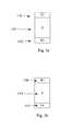
- FIGS. 1 a and 1 bare perspective views of the same memory cell comprising a junction diode and an antifuse between conductors formed at different feature sizes.
- FIGS. 2 a - 2 dare cross-sectional views illustrating fabrication of a plurality of memory cells formed according to the present invention.
- FIGS. 3 a and 3 bare cross-sectional views showing preferred configurations of p-i-n junction diodes to be used in the memory cell of the present invention.
- FIG. 4is a perspective view of a memory cell comprising a vertically oriented junction diode having no dielectric rupture antifuse disposed between top and bottom conductors.
- FIG. 5is a plan view of one possible circuit layout for a memory comprising cells formed according to the present invention.
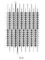
- FIGS. 6 a and 6 bare plan views of steps in the formation and preconditioning of a memory level comprising both fuse and non-fuse memory cells.
- a semiconductor junction diodefor example a p-n diode or a p-i-n diode, has been paired with a dielectric rupture antifuse to form a memory cell.
- the diodeis interposed between conductors, and a programming voltage is applied between the conductors to rupture the antifuse and program the memory cell.
- Examplesinclude the memory cells and memory arrays described in Herner et al., U.S. patent application Ser. No. 10/326,470, “An Improved Method for Making High Density Nonvolatile Memory,” filed Dec. 19, 2002 and hereinafter the '470 application; Johnson et al., U.S. Pat. No.
- junction diodeis used herein to refer to a semiconductor device with the property of conducting current more easily in one direction than the other, having two terminal electrodes, and made of semiconducting material which is p-type at one electrode and n-type at the other.
- Examplesinclude p-n diodes and n-p diodes, which have p-type semiconductor material and n-type semiconductor material in contact, and p-i-n and n-i-p diodes, in which intrinsic (undoped) semiconductor material is interposed between p-type semiconductor material and n-type semiconductor material.
- FIG. 1 ashows a device having a vertically oriented junction diode 50 disposed between conductors 52 and 54 .
- An antifuse 56is in series with the diode.
- FIG. 1 bshows the same device formed at a smaller feature size.
- programming the deviceconsists of rupturing the antifuse 56 , and then passing sufficient current through the device to form a low-resistance conductive path (or link) through the ruptured antifuse.
- the current required to program the device and form a low-resistance linkremains the same even when feature size is reduced.
- substantially the same current (and thus applied voltage)is required to rupture antifuse 56 for the device of FIG. 1 a and for the device of FIG. 1 b.
- a sufficiently high currentwill destroy such a diode, for example by melting diode 50 and physically disrupting its contact to conductors 52 or 54 or both.
- the current which will be destructive to the celldecreases with decreasing feature size of the cell.
- the cell shown in FIG. 1 bwill be destroyed or damaged at a lower current than will the cell shown in FIG. 1 a.
- the window between the programming voltage and a voltage which will be destructive to the celldecreases as feature size decreases.
- the memory cell of the present inventionaddresses this difficulty by using flow of a destructive current as the programming event.
- the unprogrammed cellis in a high-impedance state, and after programming, the programmed cell is in a low-impedance state.
- these statesare reversed:
- the unprogrammed cellis a diode interposed between conductors, and the cell is in a low-impedance state. After programming, the diode is destroyed or disrupted, and the cell is in a high impedance state.
- This memory cellis thus a fuse memory cell, rather than an antifuse memory cell.
- the memory cell of the '882 patentincludes a steering element and a state change element.
- the steering elementis realized as a diode, and in some embodiments of the '882 patent, the steering element is a fuse.
- the memory cell of the '882 patentmay be realized as a diode and a fuse in series. In the present invention, in contrast, the diode itself serves as the fuse element. The resulting memory cell is simpler and easier to fabricate.
- the ______ application(attorney docket no. MA-86-a-1) describes a memory cell having a vertically oriented junction diode, interposed between conductors, formed without a dielectric rupture antifuse. It has been found that, despite the absence of an antifuse, this cell is formed in a high-impedance state, and converts to a low-impedance state upon application of a programming voltage. While not wishing to be bound by any particular theory, it may be that application of a programming voltage to this memory cell changes the characteristics of the junction diode, which is typically formed of polycrystalline silicon (polysilicon). One possibility is that the polysilicon of the junction diode is formed in a high-resistance state, and a low-resistance filament is formed through the pillar upon application of a programming voltage.
- the junction diodeis crystallized while in contact with a silicide, the cell is low-impedance as formed.
- the silicidemay provide a template for crystal growth of the silicon, decreasing the density of silicon defects and improving the conductivity of the silicon.
- silicideby 1) depositing silicon, 2) forming an oxide, nitride, or oxynitride on the silicon, 3) forming a silicide-forming metal on the oxide, nitride, or oxynitride, then 4) annealing to reduce the oxide, nitride, or oxynitride and form the silicide by reaction of the silicide-forming metal with the silicon.
- a first embodiment of the present inventionemploys this method to form a junction diode which is low-impedance as formed and which is programmed by applying voltage sufficient to destroy or disrupt the diode.
- the '470 applicationdescribed fabrication of a monolithic three dimensional memory array comprising memory cells like those of FIGS. 1 a and 1 b.
- the '230 applicationdescribed fabrication of a monolithic three dimensional memory array comprising a related memory cell.
- the methods and procedures taught in those applications, with modifications described in this discussion,can provide guidance in formation of monolithic three dimensional memory arrays in which the memory cells comprise junction diodes. For clarity, not all of the details of the '470 and '230 applications will be included, but it will be understood that no teaching of these applications is intended to be excluded.
- This substrate 100can be any semiconducting substrate as known in the art, such as monocrystalline silicon, IV-IV compounds like silicon-germanium or silicon-germanium-carbon, III-V compounds, II-VII compounds, epitaxial layers over such substrates, or any other semiconducting material.
- the substratemay include integrated circuits fabricated therein.
- the insulating layer 102is formed over substrate 100 .
- the insulating layer 102can be silicon oxide, silicon nitride, high-dielectric film, Si—C—O—H film, or any other suitable insulating material.
- the first conductors 200are formed over the substrate and insulator.
- An adhesion layer 104may be included between the insulating layer 102 and the conducting layer 106 to help the conducting layer 106 adhere.
- Preferred materials for the adhesion layer 104are tantalum nitride, tungsten nitride, titanium tungsten, sputtered tungsten, titanium nitride, or combinations of these materials. If the overlying conducting layer is tungsten, titanium nitride is preferred as an adhesion layer.
- Conducting layer 106can comprise any conducting material known in the art, including tantalum, titanium, tungsten, copper, cobalt, or alloys thereof. Titanium nitride may be used.
- tungstenis used for conducting layer 106 , it is preferred to use a barrier layer between the tungsten and the semiconductor material that will be part of the semiconductor pillars that will eventually overlie the conductors.
- a barrier layerserves to prevent reaction between tungsten and silicon.
- the barrier layermay either be patterned with the conductor rails or with the semiconductor pillars.
- the barrier layershould be deposited after the conducting layer 106 .
- the barrier layeris not shown in FIG. 2 a .
- Any material serving this functioncan be used in the barrier layer, including tungsten nitride, tantalum nitride, titanium nitride, or combinations of these materials.
- titanium nitrideis used as the barrier layer.
- the barrier layeris titanium nitride, it can be deposited in the same manner as the adhesion layer described earlier.
- the layerswill be patterned and etched using any suitable masking and etching process to form substantially parallel, substantially coplanar conductors 200 , shown in FIG. 2 a in cross-section.
- photoresistis deposited, patterned by photolithography and the layers etched, and then the photoresist removed using standard process techniques.
- Dielectric material 108is deposited over and between conductor rails 200 .
- Dielectric material 108can be any known electrically insulating material, such as silicon oxide, silicon nitride, or silicon oxynitride. In a preferred embodiment, silicon oxide is used as dielectric material 108 .
- a barrier layer 110is to be used between the lower conductor rails and the semiconductor elements, and has not yet been formed, it will be deposited as the first layer after planarization of the conductor rails. It can be of any of the materials and deposited in any of the manners described earlier. Its thickness can be, for example, about 20 to about 500 angstroms. The thickness of barrier layer 110 is preferably about 200 angstroms.
- the semiconductor materialcan be silicon, silicon-germanium, silicon-germanium-carbon, germanium, or other suitable semiconductors or compounds. Silicon is commonly used in the industry, so, for simplicity, this description will refer to the semiconductor material as silicon, but it will be understood that other materials may be substituted.
- the semiconductor pillaris a junction diode, comprising a bottom heavily doped region of a first conductivity type and a top heavily doped region of a second conductivity type.
- the middle region, between the top and bottom regions,is an intrinsic or lightly doped region of either the first or second conductivity type.
- the diode of FIG. 3 ahas a bottom region 112 of N+ (heavily doped n-type) silicon, intrinsic region 114 , and P+ top region 116 .
- the diode of FIG. 3 bis reversed, having bottom region 112 of P+ silicon, intrinsic region 114 , and N+ top region 116 .
- the middle regionis intrinsic, or not intentionally doped, though in some embodiments it may be lightly doped.
- An undoped regionwill never be perfectly electrically neutral, and will always have defects or contaminants that cause it to behave as if slightly n-doped or p-doped.
- Such a diodecan be considered a p-i-n diode.
- a layer of heavily doped n-type silicon 112must be formed.
- This layercan be formed by any deposition and doping method known in the art.
- the siliconcan be deposited and then doped, but is preferably doped in situ by flowing a donor gas providing dopant atoms during deposition of the silicon.
- this layercan range from about 100 to about 1000 angstroms, preferably 200 angstroms, and have a dopant concentration of about 1 ⁇ 10 19 to about 2 ⁇ 10 21 atoms/cm 3 , and preferably about 8 ⁇ 10 20 atoms/cm 3 .
- the next layer 114will be intrinsic undoped silicon.
- This layercan formed by any deposition method known in the art.
- the thickness of the intrinsic silicon layercan range from about 1000 to about 4000 angstroms, preferably about 2500 angstroms.
- siliconis deposited without intentional doping, yet has defects which render it slightly n-type.
- a layer 116 of heavily doped p-type siliconis preferably deposited undoped, and will be doped by ion implantation in a later step.
- the thickness of heavily doped p-type silicon region 116can range from about 100 to about 2000 angstroms, preferably about 800 angstroms. Note this is the thickness as-deposited. Some portion of the top of this layer will be consumed in a subsequent CMP or etchback step, and will thus be thinner in the finished device.
- this layerwill preferably have a dopant concentration of about 2 ⁇ 10 19 to about 4 ⁇ 10 21 atoms/cm 3 , preferably about 8 ⁇ 10 20 atoms/cm 3 .
- forming the junction diodeincludes forming a first heavily doped silicon layer of a first conductivity type; forming a second lightly or intrinsically doped silicon layer directly on the first heavily doped layer; and forming a third heavily doped silicon layer of a second conductivity type directly on the second lightly or intrinsically doped silicon layer, the second conductivity type opposite the first.
- semiconductor layers 116 , 114 and 112 just depositedwill be patterned and etched to form semiconductor pillars 300 . If barrier layer 110 was not patterned with the bottom conductor rails, it will be patterned with the pillars. Semiconductor pillars 300 should have about the same pitch and about the same width as conductors 200 below, such that each semiconductor pillar 300 is formed on top of a conductor 200 . Some misalignment can be tolerated.
- the semiconductor pillars 300can be formed using any suitable masking and etching process.
- photoresistcan be deposited, patterned using standard photolithography techniques, and etched, then the photoresist removed.
- a hard mask of some other materialfor example silicon dioxide, can be formed on top of the semiconductor layer stack, with bottom antireflective coating (BARC) on top, then patterned and etched.
- BARCbottom antireflective coating
- DARCdielectric antireflective coating
- the pitch and width of the pillarscan be varied as desired.
- the pitch of the pillars(the distance from the center of one pillar to the center of the next pillar) is about 300 nm, while the maximum diameter of a pillar, and thus of the junction diode, varies between about 100 and about 150 nm.
- the pitch of the pillarsis about 260 nm, while the maximum diameter of a pillar varies between about 90 and 130 nm.
- the maximum diameter of the junction diodemay be less than 90 nm, for example about 50 or about 70 nm.
- Dielectric material 108is deposited over and between the semiconductor pillars 300 , filling the gaps between them.
- Dielectric material 108can be any known electrically insulating material, such as silicon oxide, silicon nitride, or silicon oxynitride. In a preferred embodiment, silicon dioxide is used as the insulating material.
- the dielectric material on top of the pillars 300is removed, exposing the tops of pillars 300 separated by dielectric material 108 , and leaving a substantially planar surface.
- This removal of dielectric overfillcan be performed by any process known in the art, such as CMP or etchback.
- the resulting structureis shown in FIG. 2 b.
- the ion implantation of heavily doped top regions 116should be performed at this point, in this example using a p-type dopant to form a P+ region.
- oxide, nitride, or oxynitride layer 118is formed on heavily doped regions 116 .
- a silicon dioxide layer 118is grown by oxidizing silicon at the tops of heavily doped regions 116 at about 600 to about 850 degrees C. for about 20 seconds to about two minutes, forming between about 15 and about 50 angstroms of silicon dioxide.
- oxide layer 118is formed by exposing the wafer to about 800 degrees for about one minute in an oxygen-containing ambient. Layer 118 could be deposited instead.
- silicide-forming metals to be used for this purposeinclude titanium, cobalt, chromium, tantalum, platinum, nickel, niobium, and palladium. This example will describe the use of titanium for layer 120 , but it will be understood that any of the other materials can be used.
- Titanium layer 120is deposited to any suitable thickness, for example between about 60 and about 200 angstroms, preferably between about 100 and about 150 angstroms, most preferably about 100 angstroms.
- titanium nitride layer 122is deposited, preferably about 300 angstroms thick. Layers 120 and 122 can be deposited by any conventional method, for example by sputtering.
- An annealis performed between about 600 and about 800 degrees from about 10 seconds to about two minutes, preferably between about 650 degrees and about 750 degrees, most preferably at about 670 degrees for about 20 seconds, for example in nitrogen.
- the annealserves to reduce oxide layer 118 and to react titanium layer 120 with heavily doped regions 116 where it overlies them to form titanium silicide.
- Oxide layer 118is substantially entirely reduced between titanium layer 120 and the silicon of heavily doped region 116 . If oxide layer 118 was deposited rather than grown, the rest of oxide layer 118 (between the tops of semiconductor pillars 300 , overlying dielectric fill 108 ) would remain. If oxide layer 118 was grown, it existed only in oxide regions 118 as shown in FIG. 2 d.
- titanium nitride layer 122 and unreacted titaniumare stripped in a selective wet etch, leaving behind titanium silicide layers 124 , each formed in a disk-shaped region on the top of one of the junction diodes 30 , shown in FIG. 2 d.
- Conventional salicide formationincludes a second anneal following strip of the unreacted titanium to convert the titanium silicide from the high-resistivity C49 phase to the low-resistivity C54 phase. In embodiments of the present invention this step is omitted. It is known that this conversion is difficult to achieve when the area of titanium silicide is very small, as in titanium silicide layers 124 . This conversion may not be necessary for the present use, and subsequent thermal processing, as additional memory levels are formed, may accomplish whatever phase conversion is achievable. In other embodiments a second anneal may be desirable.
- titanium silicide layer 124could instead be some other silicide, such as cobalt silicide, chromium silicide, tantalum silicide, platinum silicide, nickel silicide, niobium silicide, or palladium silicide.
- each pillarcomprising a silicide layer.
- Overlying conductorscan be formed in the same manner as the underlying conductors.
- the overlying conductorswill be formed at a height above the height of the first conductors, and extend in a different direction from them, preferably substantially perpendicular to them.
- Each memory cellcomprises a portion of one of the first conductors, one of the first pillars, one of the dielectric rupture antifuses, and a portion of one of the second conductors.
- the resulting structureis a bottom or first level of memory cells. Additional memory levels can be monolithically formed above the first, as described in the '470 and '230 applications and the other incorporated references, forming a monolithic three dimensional memory array.
- a second plurality of pillarscan be formed above the upper conductors, and a third plurality of conductors can be formed above them.
- the upper conductors of one memory levelcan serve as the lower conductors of an overlying memory level, or an interlevel dielectric can be formed between them.
- first conductorswere formed in a first pattern and etch step
- the pillarswere formed in a second pattern and etch step
- the second conductorswere formed in a third pattern and etch step.
- the three pattern and etch stepsare separate.
- oxide layer 118which was reduced during formation of titanium silicide layer 124 .
- Forming and reducing this layeris preferred, but the step of reducing an oxide during silicide formation is not necessary in all embodiments to form a low-impedance junction diode.
- FIGS. 3 a and 3 bTwo diode configurations were shown in FIGS. 3 a and 3 b.
- bottom region 112is in situ doped with a p-type dopant such as boron.
- a p-type dopantsuch as boron. Boron atoms tend to promote crystallization of silicon during deposition, and in most conventional silicon deposition methods, silicon heavily in situ doped with boron will be polycrystalline as deposited.
- the diode of FIG. 3 bfor example, is used in the memory cells shown being fabricated in FIGS. 2 a through 2 d, it may be that some portion of the junction diode 300 will be crystalline before silicide layer 124 is formed.
- silicide layer 124may not successfully provide a template to improve the crystallinity of the portions of the junction diode that are already crystallized.
- the junction diodeis amorphous silicon as deposited (as in the detailed example provided), and is crystallized in contact with a silicide. Note that if bottom region 112 is formed heavily doped with a p-type dopant in a way that allows it to be amorphous (doped by ion implantation, for example), it is expected that a low-impedance diode could be successfully created.
- the junction diodeis conductive and is disposed between and is in electrical contact with the top and bottom conductors. Two layers are in electrical contact if no dielectric layers intervene, and a current can pass between them.
- titanium silicide layer 124intervenes between heavily doped layer 116 at the top of each junction diode and the conductor above
- titanium nitride layer 110intervenes between heavily doped layer 112 at the bottom of each junction diode. Both silicide layer 124 and titanium nitride layer 110 are good conductors, however, so each junction diode is in electrical contact with the conductors above and below.
- the silicide layeris advantageous for reducing the impedance of the junction diode, but may not be desired in the finished device.
- the silicide layerfollowing formation of the silicide layer on the junction diode, the silicide layer can be removed.
- the overlying conductorsare then fabricated as usual.
- silicide layerformed above the junction diode, but those skilled in the art will appreciate that the silicide layer can be formed elsewhere: beside the junction diode or below it, for example. Many configurations can be imagined.
- the first embodiment of the present inventionprovides a remedy to a problem common to antifuse memories.
- An antifuse memory cellis read by applying a read voltage between the top and bottom conductors. If no current or only a very small current flows, the cell is unprogrammed; if a larger current flows, the cell is programmed. Repeated application of a read voltage to the same cell, however, can damage the antifuse, and the cumulative damage caused by many reading events may eventually unintentionally rupture it.
- programming by destruction or disruption of the celllikely occurs by a thermal mechanism, occurring when the melting point of the silicon of the diode is reached.
- the melting point of the silicon of the diodewill not be reached by application of a read voltage; thus no cumulative damage is caused to the cell no matter how many times it is read.
- a current of about 0.4 microamps or more, for example about 1.0 microamps or more, for example up to between about 50 and about 100 microampsflows between the first and second conductors.
- the resistance across the diodeis about 1 ⁇ 10 7 ohms or more, for example about 2 ⁇ 10 8 ohms or more.
- the cellis programmed by a programming voltage preferably between about 4 and about 30 volts.
- a second embodimentwill also be described.
- a memory cellis formed as described in the ______ application (attorney docket no. MA-086-a-1), the cell having no dielectric antifuse and in a high-impedance state as formed.
- Such a memory cell 3is shown in FIG. 4 .
- a first conductor 20preferably comprises titanium nitride layer 4 and tungsten layer 6 .
- Junction diode 30is formed on optional titanium nitride barrier layer 8 and comprises heavily doped semiconductor layer 10 of a first conductivity type, layer 12 which is undoped semiconductor material or lightly doped semiconductor material of a second conductivity type, and heavily doped semiconductor layer 14 of the second conductivity type.
- Second conductor 40preferably comprises titanium nitride layer 18 and tungsten layer 22 .
- this cellis in an unprogrammed, high-impedance state, and, in the ______ application (attorney docket no. MA-086-a-1), the cell is converted to a programmed, low-impedance state by application of a programming voltage.
- the present inventionis a fuse memory, in which an unprogrammed cell must be in a low-impedance state.
- a high impedance cellsuch as the cell of FIG. 4 is formed. It is then subjected to the voltage which, in the ______ application (attorney docket no. MA-086-a-1), is the programming voltage, converting it to a low-impedance state.
- this cellnow in a low-impedance state, was considered to be a programmed cell. In the present invention, however, this cell is considered to be an unprogrammed cell.
- a voltage sufficient to destroy or disrupt the diodeis applied, converting the cell from an unprogrammed, low-impedance state to a programmed, high-impedance state.
- the diodeserves as the fuse.
- the voltage that converted the cell as fabricated from its initial high-impedance state to the unprogrammed, low-impedance stateis considered to be a preconditioning voltage (in the ______ application, the same voltage was considered to be a programming voltage.)
- the voltage that converts the cell from the unprogrammed, low-impedance state to a programmed, high-impedance stateis considered the programming voltage.
- a voltageis applied across the cell, producing a current.
- the current flowing through the diodeactually induces the changes in the cell.
- the current that converted the cell as fabricated from its initial high-impedance state to the unprogrammed, low-impedance stateis considered a preconditioning current (in the ______ application (attorney docket no. MA-086-a-1), the same current acted as a programming current.)
- the current that converts the cell from the unprogrammed, low-impedance state to a programmed, high-impedance stateis considered the programming current.
- the programming voltagewill be greater than the preconditioning voltage.
- the preconditioning voltagefor example, would preferably be between about three and about eight volts, while the programming voltage would preferably be between about seven and about thirty volts.
- FIG. 5shows a plan view of one possible arrangement of a plurality of top conductors, which will here be called bitlines, and a plurality of bottom conductors, which will here be called wordlines.
- a driveris at one end of each bitline or wordline. It will be seen that the bitlines and wordlines are interleaved: driver D A is at one end of bitline A, while driver D B is at the opposite end of bitline B.
- Memory cell C NA on bitline Ais a “near bit”, a cell that is relatively close to the driver D A on that line.
- Memory cell C FA on bitline Awhich is relatively distant from the driver D A , is a “far bit”.
- memory cell C NBis a near bit on bitline B
- memory cell C FBis a far bit on bitline B. Because of its short distance from driver D A , the resistance between near bit C NA and driver D A is relatively low, while the resistance between far bit C FA and driver D A is relatively high. It is more difficult to deliver a high current to far bit C FA than it is to deliver a high current to near bit C NA .
- an array of high-impedance cells like memory cell 3 of FIG. 4can be formed.
- the arraycan be a monolithic three dimensional memory array, or could be a two-dimensional memory array.
- One memory level of such an arrayis shown in FIG. 6 a.
- High-impedance cellsare indicated by a shaded square. At this point, all of the cells are high-impedance cells.
- FIG. 6 bshows an array of unprogrammed cells.
- the preconditioned low-impedance cells (indicated by circles) in FIG. 6 bare fuse memory cells according to the present invention, which will become programmed when a programming voltage is applied, destroying or disrupting the diode and converting the cell to a high-impedance state.
- the programming voltage required to program the preconditioned fuse memory cellsis greater than the programming voltage required to program the non-preconditioned memory cells.
- a high programming voltageis required to program the near bits, where the higher voltage is easier to deliver, and a lower programming voltage is required to program the far bits, where this higher voltage is more difficult to deliver.
- the half of the bits nearer the driver on each lineare considered near bits and are preconditioned to become low-impedance fuse memory cells, while the half more distant from the driver are considered far bits and remain high impedance, non-fuse memory cells.
- the dividing line between those cells that are preconditioned and those that are notneed not be exactly half-way through the each bitline, and could be adjusted according to the actual voltages achievable at each point along each line. Further, for the sake of clarity, preconditioning was shown only along the bitline dimension. Far bits and near bits could be selectively preconditioned in the wordline direction as well.
- a monolithic three dimensional memory arrayis one in which multiple memory levels are formed above a single substrate, such as a wafer, with no intervening substrates.
- the layers forming one memory levelare deposited or grown directly over the layers of an existing level or levels.
- stacked memorieshave been constructed by forming memory levels on separate substrates and adhering the memory levels atop each other, as in Leedy, U.S. Pat. No. 5,915,167, “Three dimensional structure memory.”
- the substratesmay be thinned or removed from the memory levels before bonding, but as the memory levels are initially formed over separate substrates, such memories are not true monolithic three dimensional memory arrays.
- the present inventionhas been described herein in the context of a monolithic three dimensional memory array formed above a substrate.
- Such an arraycomprises at least a first memory level formed at a first height above the substrate and a second memory level formed at a second height different from the first height.
- Three, four, up to eight or more memory levelscan be formed above the substrate in such a multilevel array.
- Each memory levelis monolithically formed on the memory level below it.
- the memory cell of the present inventionhas been described as formed in a monolithic three dimensional memory array having stacked memory levels, but such cells could clearly be formed in a two-dimensional array, as well.
Landscapes
- Engineering & Computer Science (AREA)
- Computer Hardware Design (AREA)
- Physics & Mathematics (AREA)
- Condensed Matter Physics & Semiconductors (AREA)
- General Physics & Mathematics (AREA)
- Microelectronics & Electronic Packaging (AREA)
- Power Engineering (AREA)
- Semiconductor Memories (AREA)
Abstract
Description
- This application is related to Herner et al., U.S. application Ser. No. ______, “Junction Diode Comprising Varying Semiconductor Compositions,” (attorney docket number MA-121); to Herner et al., U.S. application Ser. No. ______, “Nonvolatile Memory Cell Without a Dielectric Antifuse Having High- and Low-Impedance States,” (attorney docket number MA-086-a-1), hereinafter the ______ application; and to Herner, U.S. application Ser. No. ______, “Memory Cell Comprising a Semiconductor Junction Diode Crystallized Adjacent to a Silicide,” (attorney docket number MA-109-1), hereinafter the ______ application; all assigned to the assignee of the present invention, all filed on even date herewith and all hereby incorporated by reference in their entirety.
- The invention relates to a fuse memory cell comprising a low-impedance diode programmed by converting the diode to a high-impedance state.
- Nonvolatile memory cells are known which employ a vertically oriented diode interposed between conductors, the diode paired with an antifuse, or having an antifuse interposed between diode portions. As formed, the cell conducts little or no current when a read voltage is applied. The cell is programmed by applying a high voltage between the conductors, across the diode and antifuse, rupturing the antifuse and creating a low-impedance path across the cell such that increased current flows between the conductors when the same read voltage is applied.
- In general, in semiconductor applications, it is advantageous to increase density, packing more devices into a smaller die area. As a memory cell pairing a diode with an antifuse is fabricated with increasingly small dimensions, the window between the energy required to program the cell and an energy sufficient to destroy the cell decreases.
- There is a need, therefore, for a nonvolatile one-time programmable memory cell that can be scaled to very small dimensions while remaining easily programmable.
- The present invention is defined by the following claims, and nothing in this section should be taken as a limitation on those claims. In general, the invention is directed to a fuse memory cell comprising a diode formed in an unprogrammed, low-impedance state which is converted to a programmed, high-impedance state, the diode itself acting as the fuse.
- A first aspect of the invention provides for a nonvolatile fuse memory cell having an unprogrammed and a programmed state, comprising a semiconductor junction diode, wherein the semiconductor junction diode operates as a fuse when the cell is converted from the unprogrammed state to the programmed state.
- Another aspect of the invention provides for a plurality of unprogrammed nonvolatile fuse memory cells comprising a plurality of substantially parallel first conductors formed at a first height above a substrate; a plurality of substantially parallel second conductors formed at a second height above the substrate, wherein the second height is different from the first height; a plurality of conductive pillars, each pillar disposed between one of the first conductors and one of the second conductors, and each pillar in electrical contact with one of the first pillars and one of the second pillars, wherein each pillar comprises a silicide layer.
- A preferred embodiment of the invention provides for a monolithic three dimensional memory array of memory cells, the array comprising: a first memory level, the first memory level comprising a first plurality of memory cells, each memory cell of the first plurality having an unprogrammed and a programmed state, each memory cell comprising a semiconductor junction diode, wherein the semiconductor junction diode operates as a fuse when the cell is converted from the unprogrammed state to the programmed state; and a second memory level, the second memory level monolithically formed above the first.
- Another preferred embodiment provides for a monolithic three dimensional memory array comprising: a first memory level formed above a substrate, the first memory level comprising: a plurality of substantially parallel lower conductors formed at a first height above the substrate; a plurality of substantially parallel upper conductors formed at a second height above the substrate, wherein the second height is above the first height; and a plurality of pillars, each pillar disposed between one of the first conductors and one of the second conductors, wherein each pillar comprises a junction diode and a silicide layer, wherein each junction diode is in electrical contact with one of the lower conductors and one of the upper conductors; and a second memory level monolithically formed above the first.
- Another aspect of the invention provides for a method for forming and programming a fuse memory cell, the method comprising: forming a memory cell, the memory cell comprising a semiconductor junction diode having an unprogrammed, low-impedance state; and programming the memory cell by converting the diode to a programmed, high-impedance state.
- Yet another aspect of the invention provides for a method for forming a plurality of unprogrammed fuse memory cells, the method comprising: forming a plurality of substantially parallel first conductors at a first height above a substrate; forming a plurality of first semiconductor junction diodes, each first semiconductor junction diode on and in electrical contact with one of the first conductors; forming a silicide layer on and in contact with each of the first semiconductor junction diodes; and forming a plurality of substantially parallel second conductors at a second height above the substrate, each silicide layer in electrical contact with one of the second conductors.
- Another preferred embodiment of the invention provides for a method for forming a monolithic three dimensional memory array, the method comprising: forming a first memory level of memory cells by a method comprising: forming a plurality of substantially parallel lower conductors at a first height above a substrate; forming a plurality of substantially parallel upper conductors at a second height above the substrate, the second height above the first; and forming a plurality of pillars, each pillar disposed between and in electrical contact with one of the first conductors and one of the second conductors, wherein each pillar comprises a silicide layer; and monolithically forming a second memory level above the first.
- Each of the aspects and embodiments of the invention described herein can be used alone or in combination with one another.
- The preferred aspects and embodiments will now be described with reference to the attached drawings.
FIGS. 1 aand1bare perspective views of the same memory cell comprising a junction diode and an antifuse between conductors formed at different feature sizes.FIGS. 2 a-2dare cross-sectional views illustrating fabrication of a plurality of memory cells formed according to the present invention.FIGS. 3 aand3bare cross-sectional views showing preferred configurations of p-i-n junction diodes to be used in the memory cell of the present invention.FIG. 4 is a perspective view of a memory cell comprising a vertically oriented junction diode having no dielectric rupture antifuse disposed between top and bottom conductors.FIG. 5 is a plan view of one possible circuit layout for a memory comprising cells formed according to the present invention.FIGS. 6 aand6bare plan views of steps in the formation and preconditioning of a memory level comprising both fuse and non-fuse memory cells.- A semiconductor junction diode, for example a p-n diode or a p-i-n diode, has been paired with a dielectric rupture antifuse to form a memory cell. The diode is interposed between conductors, and a programming voltage is applied between the conductors to rupture the antifuse and program the memory cell. Examples include the memory cells and memory arrays described in Herner et al., U.S. patent application Ser. No. 10/326,470, “An Improved Method for Making High Density Nonvolatile Memory,” filed Dec. 19, 2002 and hereinafter the '470 application; Johnson et al., U.S. Pat. No. 6,034,882, “Vertically stacked field programmable nonvolatile memory and method of fabrication,” and hereinafter the '882 patent; Johnson, U.S. Pat. No. 6,525,953, “Vertically stacked field programmable nonvolatile memory and method of fabrication”; Knall et al., U.S. Pat. No. 6,420,215, “Three Dimensional Memory Array and Method of Fabrication”; Vyvoda et al., U.S. patent application Ser. No. 10/185507, “Electrically Isolated Pillars in Active Devices,” filed Jun. 27, 2002; Cleeves et al., “Optimization of Critical Dimensions and Pitch of Patterned Features in and Above a Substrate,” U.S. patent application Ser. No. 10/728,451, filed Dec. 5, 2003; Petti et al., U.S. patent application Ser. No. 10/728230, “Semiconductor Device Including Junction Diode Contacting Contact-Antifuse Unit Comprising Silicide,” filed Dec. 3, 2002, hereinafter the '230 application, all assigned to the assignee of the present invention and all hereby incorporated by reference.
- The term junction diode is used herein to refer to a semiconductor device with the property of conducting current more easily in one direction than the other, having two terminal electrodes, and made of semiconducting material which is p-type at one electrode and n-type at the other. Examples include p-n diodes and n-p diodes, which have p-type semiconductor material and n-type semiconductor material in contact, and p-i-n and n-i-p diodes, in which intrinsic (undoped) semiconductor material is interposed between p-type semiconductor material and n-type semiconductor material.
FIG. 1 ashows a device having a verticallyoriented junction diode 50 disposed betweenconductors antifuse 56 is in series with the diode.FIG. 1 bshows the same device formed at a smaller feature size. In general, in a device having a vertically oriented diode, programming the device consists of rupturing theantifuse 56, and then passing sufficient current through the device to form a low-resistance conductive path (or link) through the ruptured antifuse. The current required to program the device and form a low-resistance link remains the same even when feature size is reduced. Thus, for a given programming time, substantially the same current (and thus applied voltage) is required to ruptureantifuse 56 for the device ofFIG. 1 aand for the device ofFIG. 1 b.- A sufficiently high current, however, will destroy such a diode, for example by melting
diode 50 and physically disrupting its contact toconductors FIG. 1 bwill be destroyed or damaged at a lower current than will the cell shown inFIG. 1 a.Thus the window between the programming voltage and a voltage which will be destructive to the cell decreases as feature size decreases. - The memory cell of the present invention addresses this difficulty by using flow of a destructive current as the programming event. In the memory cells discussed so far, the unprogrammed cell is in a high-impedance state, and after programming, the programmed cell is in a low-impedance state. In the present invention, these states are reversed: The unprogrammed cell is a diode interposed between conductors, and the cell is in a low-impedance state. After programming, the diode is destroyed or disrupted, and the cell is in a high impedance state.
- This memory cell is thus a fuse memory cell, rather than an antifuse memory cell. The memory cell of the '882 patent includes a steering element and a state change element. In most embodiments the steering element is realized as a diode, and in some embodiments of the '882 patent, the steering element is a fuse. Thus the memory cell of the '882 patent may be realized as a diode and a fuse in series. In the present invention, in contrast, the diode itself serves as the fuse element. The resulting memory cell is simpler and easier to fabricate.
- The ______ application (attorney docket no. MA-86-a-1) describes a memory cell having a vertically oriented junction diode, interposed between conductors, formed without a dielectric rupture antifuse. It has been found that, despite the absence of an antifuse, this cell is formed in a high-impedance state, and converts to a low-impedance state upon application of a programming voltage. While not wishing to be bound by any particular theory, it may be that application of a programming voltage to this memory cell changes the characteristics of the junction diode, which is typically formed of polycrystalline silicon (polysilicon). One possibility is that the polysilicon of the junction diode is formed in a high-resistance state, and a low-resistance filament is formed through the pillar upon application of a programming voltage.
- As taught in the ______ application (attorney docket no. MA-109-1), it has been found that if the junction diode is crystallized while in contact with a silicide, the cell is low-impedance as formed. The silicide may provide a template for crystal growth of the silicon, decreasing the density of silicon defects and improving the conductivity of the silicon. It is particularly advantageous to form the silicide by 1) depositing silicon, 2) forming an oxide, nitride, or oxynitride on the silicon, 3) forming a silicide-forming metal on the oxide, nitride, or oxynitride, then 4) annealing to reduce the oxide, nitride, or oxynitride and form the silicide by reaction of the silicide-forming metal with the silicon.
- A first embodiment of the present invention employs this method to form a junction diode which is low-impedance as formed and which is programmed by applying voltage sufficient to destroy or disrupt the diode.
- A detailed example will be provided of fabrication of an array of memory cells formed according to aspects of the present invention. For completeness, many details of materials, process conditions, and steps will be provided. It will be understood, however, that many details can be changed, omitted or supplemented while the results fall within the scope of the invention.
- The '470 application described fabrication of a monolithic three dimensional memory array comprising memory cells like those of
FIGS. 1 aand1b.The '230 application described fabrication of a monolithic three dimensional memory array comprising a related memory cell. The methods and procedures taught in those applications, with modifications described in this discussion, can provide guidance in formation of monolithic three dimensional memory arrays in which the memory cells comprise junction diodes. For clarity, not all of the details of the '470 and '230 applications will be included, but it will be understood that no teaching of these applications is intended to be excluded. - Fabrication of a single memory level is described in detail. Additional memory levels can be stacked, each monolithically formed above the one below it.
- Turning to
FIG. 2 a,formation of the memory begins with asubstrate 100. Thissubstrate 100 can be any semiconducting substrate as known in the art, such as monocrystalline silicon, IV-IV compounds like silicon-germanium or silicon-germanium-carbon, III-V compounds, II-VII compounds, epitaxial layers over such substrates, or any other semiconducting material. The substrate may include integrated circuits fabricated therein. - An insulating
layer 102 is formed oversubstrate 100. The insulatinglayer 102 can be silicon oxide, silicon nitride, high-dielectric film, Si—C—O—H film, or any other suitable insulating material. - The
first conductors 200 are formed over the substrate and insulator. Anadhesion layer 104 may be included between the insulatinglayer 102 and theconducting layer 106 to help theconducting layer 106 adhere. Preferred materials for theadhesion layer 104 are tantalum nitride, tungsten nitride, titanium tungsten, sputtered tungsten, titanium nitride, or combinations of these materials. If the overlying conducting layer is tungsten, titanium nitride is preferred as an adhesion layer. - The next layer to be deposited is conducting
layer 106. Conductinglayer 106 can comprise any conducting material known in the art, including tantalum, titanium, tungsten, copper, cobalt, or alloys thereof. Titanium nitride may be used. - If tungsten is used for conducting
layer 106, it is preferred to use a barrier layer between the tungsten and the semiconductor material that will be part of the semiconductor pillars that will eventually overlie the conductors. Such a barrier layer serves to prevent reaction between tungsten and silicon. The barrier layer may either be patterned with the conductor rails or with the semiconductor pillars. - If a barrier layer is to be used, and is to be formed as the top layer of the conductor rails, the barrier layer should be deposited after the
conducting layer 106. (The barrier layer is not shown inFIG. 2 a.) Any material serving this function can be used in the barrier layer, including tungsten nitride, tantalum nitride, titanium nitride, or combinations of these materials. In a preferred embodiment, titanium nitride is used as the barrier layer. Where the barrier layer is titanium nitride, it can be deposited in the same manner as the adhesion layer described earlier. - Once all the layers that will form the conductor rails have been deposited, the layers will be patterned and etched using any suitable masking and etching process to form substantially parallel, substantially
coplanar conductors 200, shown inFIG. 2 ain cross-section. In one embodiment, photoresist is deposited, patterned by photolithography and the layers etched, and then the photoresist removed using standard process techniques. - Next a
dielectric material 108 is deposited over and between conductor rails200.Dielectric material 108 can be any known electrically insulating material, such as silicon oxide, silicon nitride, or silicon oxynitride. In a preferred embodiment, silicon oxide is used asdielectric material 108. - Finally, excess
dielectric material 108 on top ofconductor rails 200 is removed, exposing the tops ofconductor rails 200 separated bydielectric material 108, and leaving a substantiallyplanar surface 109. The resulting structure is shown inFIG. 2 a.This removal of dielectric overfill to formplanar surface 109 can be performed by any process known in the art, such as chemical mechanical planarization (CMP) or etchback. At this stage, a plurality of substantially parallel first conductors have been formed at a first height abovesubstrate 100. - Next, turning to
FIG. 2 b,vertical semiconductor pillars will be formed above completed conductor rails200. (To savespace substrate 100 is omitted inFIG. 2 b;its presence will be assumed.) If abarrier layer 110 is to be used between the lower conductor rails and the semiconductor elements, and has not yet been formed, it will be deposited as the first layer after planarization of the conductor rails. It can be of any of the materials and deposited in any of the manners described earlier. Its thickness can be, for example, about 20 to about 500 angstroms. The thickness ofbarrier layer 110 is preferably about 200 angstroms. - Next semiconductor material that will be patterned into pillars is deposited. The semiconductor material can be silicon, silicon-germanium, silicon-germanium-carbon, germanium, or other suitable semiconductors or compounds. Silicon is commonly used in the industry, so, for simplicity, this description will refer to the semiconductor material as silicon, but it will be understood that other materials may be substituted.
- In preferred embodiments, the semiconductor pillar is a junction diode, comprising a bottom heavily doped region of a first conductivity type and a top heavily doped region of a second conductivity type. The middle region, between the top and bottom regions, is an intrinsic or lightly doped region of either the first or second conductivity type. The diode of
FIG. 3 ahas abottom region 112 of N+ (heavily doped n-type) silicon,intrinsic region 114, and P+top region 116. The diode ofFIG. 3 bis reversed, havingbottom region 112 of P+ silicon,intrinsic region 114, and N+top region 116. The middle region is intrinsic, or not intentionally doped, though in some embodiments it may be lightly doped. An undoped region will never be perfectly electrically neutral, and will always have defects or contaminants that cause it to behave as if slightly n-doped or p-doped. Such a diode can be considered a p-i-n diode. - To form, for example, the diode of
FIG. 3 a,a layer of heavily doped n-type silicon 112 must be formed. This layer can be formed by any deposition and doping method known in the art. The silicon can be deposited and then doped, but is preferably doped in situ by flowing a donor gas providing dopant atoms during deposition of the silicon. In a preferred embodiment, this layer can range from about 100 to about 1000 angstroms, preferably 200 angstroms, and have a dopant concentration of about 1×10¹⁹to about 2×10²¹atoms/cm3, and preferably about 8×10²⁰atoms/cm3. - The
next layer 114 will be intrinsic undoped silicon. This layer can formed by any deposition method known in the art. The thickness of the intrinsic silicon layer can range from about 1000 to about 4000 angstroms, preferably about 2500 angstroms. In one embodiment, silicon is deposited without intentional doping, yet has defects which render it slightly n-type. - Above this is a
layer 116 of heavily doped p-type silicon. This layer is preferably deposited undoped, and will be doped by ion implantation in a later step. The thickness of heavily doped p-type silicon region 116 can range from about 100 to about 2000 angstroms, preferably about 800 angstroms. Note this is the thickness as-deposited. Some portion of the top of this layer will be consumed in a subsequent CMP or etchback step, and will thus be thinner in the finished device. After implantation, this layer will preferably have a dopant concentration of about 2×10¹⁹to about 4×10²¹atoms/cm3, preferably about 8×10²⁰atoms/cm3. - To summarize, forming the junction diode includes forming a first heavily doped silicon layer of a first conductivity type; forming a second lightly or intrinsically doped silicon layer directly on the first heavily doped layer; and forming a third heavily doped silicon layer of a second conductivity type directly on the second lightly or intrinsically doped silicon layer, the second conductivity type opposite the first.
- Returning to
FIG. 2 b,semiconductor layers116,114 and112 just deposited will be patterned and etched to formsemiconductor pillars 300. Ifbarrier layer 110 was not patterned with the bottom conductor rails, it will be patterned with the pillars.Semiconductor pillars 300 should have about the same pitch and about the same width asconductors 200 below, such that eachsemiconductor pillar 300 is formed on top of aconductor 200. Some misalignment can be tolerated. - The
semiconductor pillars 300 can be formed using any suitable masking and etching process. For example, photoresist can be deposited, patterned using standard photolithography techniques, and etched, then the photoresist removed. Alternatively, a hard mask of some other material, for example silicon dioxide, can be formed on top of the semiconductor layer stack, with bottom antireflective coating (BARC) on top, then patterned and etched. Similarly, dielectric antireflective coating (DARC) can be used as a hard mask. - The photolithography techniques described in Chen, U.S. application Ser. No. 10/728436, “Photomask Features with Interior Nonprinting Window Using Alternating Phase Shifting,” filed Dec. 5, 2003; or Chen, U.S. application Ser. No. 10/815312, Photomask Features with Chromeless Nonprinting Phase Shifting Window,” filed Apr. 1, 2004, both owned by the assignee of the present invention and hereby incorporated by reference, can advantageously be used to perform any photolithography step used in formation of a memory array according to the present invention.
- The pitch and width of the pillars can be varied as desired. In one preferred embodiment, the pitch of the pillars (the distance from the center of one pillar to the center of the next pillar) is about 300 nm, while the maximum diameter of a pillar, and thus of the junction diode, varies between about 100 and about 150 nm. In another preferred embodiment, the pitch of the pillars is about 260 nm, while the maximum diameter of a pillar varies between about 90 and 130 nm. The maximum diameter of the junction diode may be less than 90 nm, for example about 50 or about 70 nm.
Dielectric material 108 is deposited over and between thesemiconductor pillars 300, filling the gaps between them.Dielectric material 108 can be any known electrically insulating material, such as silicon oxide, silicon nitride, or silicon oxynitride. In a preferred embodiment, silicon dioxide is used as the insulating material.- Next the dielectric material on top of the
pillars 300 is removed, exposing the tops ofpillars 300 separated bydielectric material 108, and leaving a substantially planar surface. This removal of dielectric overfill can be performed by any process known in the art, such as CMP or etchback. The resulting structure is shown inFIG. 2 b.The ion implantation of heavily dopedtop regions 116 should be performed at this point, in this example using a p-type dopant to form a P+ region. - Turning to
FIG. 2 c,next an oxide, nitride, oroxynitride layer 118 is formed on heavily dopedregions 116. In preferred embodiments, as shown, asilicon dioxide layer 118 is grown by oxidizing silicon at the tops of heavily dopedregions 116 at about 600 to about 850 degrees C. for about 20 seconds to about two minutes, forming between about 15 and about 50 angstroms of silicon dioxide. Preferably,oxide layer 118 is formed by exposing the wafer to about 800 degrees for about one minute in an oxygen-containing ambient.Layer 118 could be deposited instead. - Next a
layer 120 of a silicide-forming metal is deposited. Preferred silicide-forming metals to be used for this purpose include titanium, cobalt, chromium, tantalum, platinum, nickel, niobium, and palladium. This example will describe the use of titanium forlayer 120, but it will be understood that any of the other materials can be used. Titanium layer 120 is deposited to any suitable thickness, for example between about 60 and about 200 angstroms, preferably between about 100 and about 150 angstroms, most preferably about 100 angstroms. To prevent oxidation oftitanium layer 120,titanium nitride layer 122 is deposited, preferably about 300 angstroms thick.Layers - An anneal is performed between about 600 and about 800 degrees from about 10 seconds to about two minutes, preferably between about 650 degrees and about 750 degrees, most preferably at about 670 degrees for about 20 seconds, for example in nitrogen. The anneal serves to reduce
oxide layer 118 and to reacttitanium layer 120 with heavily dopedregions 116 where it overlies them to form titanium silicide.Oxide layer 118 is substantially entirely reduced betweentitanium layer 120 and the silicon of heavily dopedregion 116. Ifoxide layer 118 was deposited rather than grown, the rest of oxide layer118 (between the tops ofsemiconductor pillars 300, overlying dielectric fill108) would remain. Ifoxide layer 118 was grown, it existed only inoxide regions 118 as shown inFIG. 2 d. - As in a conventional salicide process,
titanium nitride layer 122 and unreacted titanium are stripped in a selective wet etch, leaving behindtitanium silicide layers 124, each formed in a disk-shaped region on the top of one of thejunction diodes 30, shown inFIG. 2 d. - Conventional salicide formation includes a second anneal following strip of the unreacted titanium to convert the titanium silicide from the high-resistivity C49 phase to the low-resistivity C54 phase. In embodiments of the present invention this step is omitted. It is known that this conversion is difficult to achieve when the area of titanium silicide is very small, as in titanium silicide layers124. This conversion may not be necessary for the present use, and subsequent thermal processing, as additional memory levels are formed, may accomplish whatever phase conversion is achievable. In other embodiments a second anneal may be desirable.
- As noted, in this example it is assumed that titanium is used in the silicide-forming
metal layer 120, but other materials, including cobalt, chromium, tantalum, platinum, nickel, niobium, and palladium, could have been used instead. Thustitanium silicide layer 124 could instead be some other silicide, such as cobalt silicide, chromium silicide, tantalum silicide, platinum silicide, nickel silicide, niobium silicide, or palladium silicide. - At this point a plurality of first pillars has been formed above the first conductors, each pillar comprising a silicide layer.
- Overlying conductors can be formed in the same manner as the underlying conductors. The overlying conductors will be formed at a height above the height of the first conductors, and extend in a different direction from them, preferably substantially perpendicular to them. Each memory cell comprises a portion of one of the first conductors, one of the first pillars, one of the dielectric rupture antifuses, and a portion of one of the second conductors. The resulting structure is a bottom or first level of memory cells. Additional memory levels can be monolithically formed above the first, as described in the '470 and '230 applications and the other incorporated references, forming a monolithic three dimensional memory array. For example, a second plurality of pillars can be formed above the upper conductors, and a third plurality of conductors can be formed above them. The upper conductors of one memory level can serve as the lower conductors of an overlying memory level, or an interlevel dielectric can be formed between them.
- It will be noted that the first conductors were formed in a first pattern and etch step, the pillars were formed in a second pattern and etch step, and the second conductors were formed in a third pattern and etch step. The three pattern and etch steps are separate. Prior art three dimensional memories, such as the '882 patent, form analogous structures in pattern and etch steps that overlap.
- The example just provided included formation of
oxide layer 118 which was reduced during formation oftitanium silicide layer 124. Forming and reducing this layer is preferred, but the step of reducing an oxide during silicide formation is not necessary in all embodiments to form a low-impedance junction diode. - Two diode configurations were shown in
FIGS. 3 aand3b.InFIG. 3 b,bottom region 112 is in situ doped with a p-type dopant such as boron. Boron atoms tend to promote crystallization of silicon during deposition, and in most conventional silicon deposition methods, silicon heavily in situ doped with boron will be polycrystalline as deposited. If the diode ofFIG. 3 b,for example, is used in the memory cells shown being fabricated inFIGS. 2 athrough2d,it may be that some portion of thejunction diode 300 will be crystalline beforesilicide layer 124 is formed. In this case,silicide layer 124 may not successfully provide a template to improve the crystallinity of the portions of the junction diode that are already crystallized. In preferred embodiments, the junction diode is amorphous silicon as deposited (as in the detailed example provided), and is crystallized in contact with a silicide. Note that ifbottom region 112 is formed heavily doped with a p-type dopant in a way that allows it to be amorphous (doped by ion implantation, for example), it is expected that a low-impedance diode could be successfully created. - In the memory cell just described, as formed, the junction diode is conductive and is disposed between and is in electrical contact with the top and bottom conductors. Two layers are in electrical contact if no dielectric layers intervene, and a current can pass between them. Referring to
FIG. 2 d,titanium silicide layer 124 intervenes between heavily dopedlayer 116 at the top of each junction diode and the conductor above, andtitanium nitride layer 110 intervenes between heavily dopedlayer 112 at the bottom of each junction diode. Bothsilicide layer 124 andtitanium nitride layer 110 are good conductors, however, so each junction diode is in electrical contact with the conductors above and below. - The silicide layer is advantageous for reducing the impedance of the junction diode, but may not be desired in the finished device. In an alternative embodiment, following formation of the silicide layer on the junction diode, the silicide layer can be removed. The overlying conductors are then fabricated as usual.
- The example given showed the silicide layer formed above the junction diode, but those skilled in the art will appreciate that the silicide layer can be formed elsewhere: beside the junction diode or below it, for example. Many configurations can be imagined.
- The first embodiment of the present invention, just described, provides a remedy to a problem common to antifuse memories. An antifuse memory cell is read by applying a read voltage between the top and bottom conductors. If no current or only a very small current flows, the cell is unprogrammed; if a larger current flows, the cell is programmed. Repeated application of a read voltage to the same cell, however, can damage the antifuse, and the cumulative damage caused by many reading events may eventually unintentionally rupture it.
- In the embodiment of the present invention just described, however, programming by destruction or disruption of the cell likely occurs by a thermal mechanism, occurring when the melting point of the silicon of the diode is reached. The melting point of the silicon of the diode will not be reached by application of a read voltage; thus no cumulative damage is caused to the cell no matter how many times it is read.
- When this memory is complete, in the unprogrammed, low-impedance state, upon application of a read voltage between the first and second conductors of between about 0.5 and about 3 volts, a current of about 0.4 microamps or more, for example about 1.0 microamps or more, for example up to between about 50 and about 100 microamps, flows between the first and second conductors. In the programmed, high-impedance state, the resistance across the diode is about 1×10⁷ohms or more, for example about 2×10⁸ohms or more. The cell is programmed by a programming voltage preferably between about 4 and about 30 volts.
- A second embodiment will also be described. In this embodiment a memory cell is formed as described in the ______ application (attorney docket no. MA-086-a-1), the cell having no dielectric antifuse and in a high-impedance state as formed. Such a
memory cell 3 is shown inFIG. 4 . Afirst conductor 20 preferably comprisestitanium nitride layer 4 andtungsten layer 6.Junction diode 30 is formed on optional titaniumnitride barrier layer 8 and comprises heavily dopedsemiconductor layer 10 of a first conductivity type,layer 12 which is undoped semiconductor material or lightly doped semiconductor material of a second conductivity type, and heavily dopedsemiconductor layer 14 of the second conductivity type.Second conductor 40 preferably comprisestitanium nitride layer 18 andtungsten layer 22. - As formed, this cell is in an unprogrammed, high-impedance state, and, in the ______ application (attorney docket no. MA-086-a-1), the cell is converted to a programmed, low-impedance state by application of a programming voltage.
- The present invention, however, is a fuse memory, in which an unprogrammed cell must be in a low-impedance state. In the present invention, a high impedance cell such as the cell of
FIG. 4 is formed. It is then subjected to the voltage which, in the ______ application (attorney docket no. MA-086-a-1), is the programming voltage, converting it to a low-impedance state. - In the ______ application (attorney docket no. MA-086-a-1), this cell, now in a low-impedance state, was considered to be a programmed cell. In the present invention, however, this cell is considered to be an unprogrammed cell. At a later time, when the cell is to be programmed, a voltage sufficient to destroy or disrupt the diode is applied, converting the cell from an unprogrammed, low-impedance state to a programmed, high-impedance state. The diode serves as the fuse. In this case, the voltage that converted the cell as fabricated from its initial high-impedance state to the unprogrammed, low-impedance state is considered to be a preconditioning voltage (in the ______ application, the same voltage was considered to be a programming voltage.) The voltage that converts the cell from the unprogrammed, low-impedance state to a programmed, high-impedance state is considered the programming voltage.
- A voltage is applied across the cell, producing a current. The current flowing through the diode actually induces the changes in the cell. Alternatively, then, it could be said that the current that converted the cell as fabricated from its initial high-impedance state to the unprogrammed, low-impedance state is considered a preconditioning current (in the ______ application (attorney docket no. MA-086-a-1), the same current acted as a programming current.) The current that converts the cell from the unprogrammed, low-impedance state to a programmed, high-impedance state is considered the programming current.
- In general, the programming voltage will be greater than the preconditioning voltage. The preconditioning voltage, for example, would preferably be between about three and about eight volts, while the programming voltage would preferably be between about seven and about thirty volts.
- As has been described, cells are interposed between top and bottom conductors.
FIG. 5 shows a plan view of one possible arrangement of a plurality of top conductors, which will here be called bitlines, and a plurality of bottom conductors, which will here be called wordlines. A driver is at one end of each bitline or wordline. It will be seen that the bitlines and wordlines are interleaved: driver DAis at one end of bitline A, while driver DBis at the opposite end of bitline B. - Memory cell CNAon bitline A is a “near bit”, a cell that is relatively close to the driver DAon that line. Memory cell CFAon bitline A, which is relatively distant from the driver DA, is a “far bit”. Similarly, memory cell CNBis a near bit on bitline B, while memory cell CFBis a far bit on bitline B. Because of its short distance from driver DA, the resistance between near bit CNAand driver DAis relatively low, while the resistance between far bit CFAand driver DAis relatively high. It is more difficult to deliver a high current to far bit CFAthan it is to deliver a high current to near bit CNA.
- In a preferred embodiment, then, it may be advantageous to combine fuse and non-fuse memory cells in the same array. In this way the near bits can be programmed with a high voltage, while the far bits are programmed with a lower voltage.
- For example, an array of high-impedance cells like
memory cell 3 ofFIG. 4 can be formed. The array can be a monolithic three dimensional memory array, or could be a two-dimensional memory array. One memory level of such an array is shown inFIG. 6 a.High-impedance cells are indicated by a shaded square. At this point, all of the cells are high-impedance cells. - Next the near bits on each bitline are subjected to a preconditioning voltage to convert them to a low-impedance state, indicated by a circle, shown in
FIG. 6 b.The far bits remain in the initial, high-impedance state.FIG. 6 bshows an array of unprogrammed cells. The preconditioned low-impedance cells (indicated by circles) inFIG. 6 bare fuse memory cells according to the present invention, which will become programmed when a programming voltage is applied, destroying or disrupting the diode and converting the cell to a high-impedance state. The non-preconditioned, high-impedance cells inFIG. 6 b(indicated by squares) are not fuse memory cells, and will become programmed when a programming voltage is applied, converting each high-impedance cell to a low-impedance state. The programming voltage required to program the preconditioned fuse memory cells is greater than the programming voltage required to program the non-preconditioned memory cells. Thus a high programming voltage is required to program the near bits, where the higher voltage is easier to deliver, and a lower programming voltage is required to program the far bits, where this higher voltage is more difficult to deliver. - In this example the half of the bits nearer the driver on each line are considered near bits and are preconditioned to become low-impedance fuse memory cells, while the half more distant from the driver are considered far bits and remain high impedance, non-fuse memory cells. Clearly the dividing line between those cells that are preconditioned and those that are not need not be exactly half-way through the each bitline, and could be adjusted according to the actual voltages achievable at each point along each line. Further, for the sake of clarity, preconditioning was shown only along the bitline dimension. Far bits and near bits could be selectively preconditioned in the wordline direction as well.
- A monolithic three dimensional memory array is one in which multiple memory levels are formed above a single substrate, such as a wafer, with no intervening substrates. The layers forming one memory level are deposited or grown directly over the layers of an existing level or levels. In contrast, stacked memories have been constructed by forming memory levels on separate substrates and adhering the memory levels atop each other, as in Leedy, U.S. Pat. No. 5,915,167, “Three dimensional structure memory.” The substrates may be thinned or removed from the memory levels before bonding, but as the memory levels are initially formed over separate substrates, such memories are not true monolithic three dimensional memory arrays.
- The present invention has been described herein in the context of a monolithic three dimensional memory array formed above a substrate. Such an array comprises at least a first memory level formed at a first height above the substrate and a second memory level formed at a second height different from the first height. Three, four, up to eight or more memory levels can be formed above the substrate in such a multilevel array. Each memory level is monolithically formed on the memory level below it.
- The memory cell of the present invention has been described as formed in a monolithic three dimensional memory array having stacked memory levels, but such cells could clearly be formed in a two-dimensional array, as well.
- Detailed methods of fabrication have been described herein, but any other methods that form the same structures can be used while the results fall within the scope of the invention.
- The foregoing detailed description has described only a few of the many forms that this invention can take. For this reason, this detailed description is intended by way of illustration, and not by way of limitation. It is only the following claims, including all equivalents, which are intended to define the scope of this invention.
Claims (80)
Priority Applications (5)
| Application Number | Priority Date | Filing Date | Title |
|---|---|---|---|
| US10/955,387US20060067117A1 (en) | 2004-09-29 | 2004-09-29 | Fuse memory cell comprising a diode, the diode serving as the fuse element |
| KR1020077004309AKR20070106962A (en) | 2004-09-29 | 2005-09-28 | Fuse memory cells with diodes, and diodes acting as fuse elements |
| EP05800174AEP1803129A4 (en) | 2004-09-29 | 2005-09-28 | Fuse memory cell comprising a diode, the diode serving as the fuse element |
| PCT/US2005/034936WO2006039370A2 (en) | 2004-09-29 | 2005-09-28 | Fuse memory cell comprising a diode, the diode serving as the fuse element |
| CNA200580026092XACN101432823A (en) | 2004-09-29 | 2005-09-28 | Fuse memory cell comprising a diode, the diode serving as the fuse element |
Applications Claiming Priority (1)
| Application Number | Priority Date | Filing Date | Title |
|---|---|---|---|
| US10/955,387US20060067117A1 (en) | 2004-09-29 | 2004-09-29 | Fuse memory cell comprising a diode, the diode serving as the fuse element |
Publications (1)
| Publication Number | Publication Date |
|---|---|
| US20060067117A1true US20060067117A1 (en) | 2006-03-30 |
Family
ID=36098853
Family Applications (1)
| Application Number | Title | Priority Date | Filing Date |
|---|---|---|---|
| US10/955,387AbandonedUS20060067117A1 (en) | 2004-09-29 | 2004-09-29 | Fuse memory cell comprising a diode, the diode serving as the fuse element |
Country Status (5)
| Country | Link |
|---|---|
| US (1) | US20060067117A1 (en) |
| EP (1) | EP1803129A4 (en) |
| KR (1) | KR20070106962A (en) |
| CN (1) | CN101432823A (en) |
| WO (1) | WO2006039370A2 (en) |
Cited By (38)
| Publication number | Priority date | Publication date | Assignee | Title |
|---|---|---|---|---|
| US20050052915A1 (en)* | 2002-12-19 | 2005-03-10 | Matrix Semiconductor, Inc. | Nonvolatile memory cell without a dielectric antifuse having high- and low-impedance states |
| US20050226067A1 (en)* | 2002-12-19 | 2005-10-13 | Matrix Semiconductor, Inc. | Nonvolatile memory cell operating by increasing order in polycrystalline semiconductor material |
| US20060250837A1 (en)* | 2005-05-09 | 2006-11-09 | Sandisk 3D, Llc | Nonvolatile memory cell comprising a diode and a resistance-switching material |
| US20070069217A1 (en)* | 2003-12-03 | 2007-03-29 | Herner S B | P-i-n diode crystallized adjacent to a silicide in series with a dielectric anitfuse |
| US20070105284A1 (en)* | 2003-12-03 | 2007-05-10 | Herner S B | Method for forming a memory cell comprising a semiconductor junction diode crystallized adjacent to a silicide |
| US20070114508A1 (en)* | 2005-11-23 | 2007-05-24 | Matrix Semiconductor, Inc. | Reversible resistivity-switching metal oxide or nitride layer with added metal |
| US20070114509A1 (en)* | 2005-11-23 | 2007-05-24 | Sandisk 3D Llc | Memory cell comprising nickel-cobalt oxide switching element |
| US20070228414A1 (en)* | 2006-03-31 | 2007-10-04 | Sandisk 3D, Llc | Heterojunction device comprising a semiconductor and a resistivity-switching oxide or nitride |
| US20070228354A1 (en)* | 2006-03-31 | 2007-10-04 | Sandisk 3D, Llc | Nonvolatile rewritable memory cell comprising a resistivity-switching oxide or nitride and an antifuse |
| US20070236981A1 (en)* | 2006-03-31 | 2007-10-11 | Sandisk 3D, Llc | Multilevel nonvolatile memory cell comprising a resistivity-switching oxide or nitride and an antifuse |
| WO2007141738A1 (en)* | 2006-06-09 | 2007-12-13 | Nxp B.V. | A semiconductor fuse structure and a method of manufacturing a semiconductor fuse structure |
| US20080025061A1 (en)* | 2006-07-31 | 2008-01-31 | Scheuerlein Roy E | High bandwidth one time field-programmable memory |
| US20080025067A1 (en)* | 2006-07-31 | 2008-01-31 | Scheuerlein Roy E | Systems for high bandwidth one time field-programmable memory |
| US20080025068A1 (en)* | 2006-07-31 | 2008-01-31 | Scheuerlein Roy E | Reverse bias trim operations in non-volatile memory |
| US20080025077A1 (en)* | 2006-07-31 | 2008-01-31 | Scheuerlein Roy E | Systems for controlled pulse operations in non-volatile memory |
| US20080025078A1 (en)* | 2006-07-31 | 2008-01-31 | Scheuerlein Roy E | Systems for reverse bias trim operations in non-volatile memory |
| US20080025076A1 (en)* | 2006-07-31 | 2008-01-31 | Scheuerlein Roy E | Controlled pulse operations in non-volatile memory |
| US20080094916A1 (en)* | 2006-10-24 | 2008-04-24 | Fasoli Luca G | Memory device for controlling current during programming of memory cells |
| US20080094915A1 (en)* | 2006-10-24 | 2008-04-24 | Fasoli Luca G | Method for controlling current during programming of memory cells |
| US7391638B2 (en) | 2006-10-24 | 2008-06-24 | Sandisk 3D Llc | Memory device for protecting memory cells during programming |
| US20080254615A1 (en)* | 2005-03-25 | 2008-10-16 | Dunton Samuel V | Method for reducing dielectric overetch using a dielectric etch stop at a planar surface |
| US20090001344A1 (en)* | 2007-06-29 | 2009-01-01 | April Schricker | Memory cell that employs a selectively grown reversible resistance-switching element and methods of forming the same |
| US20090001343A1 (en)* | 2007-06-29 | 2009-01-01 | April Schricker | Memory cell that employs a selectively deposited reversible resistance-switching element and methods of forming the same |
| US20090001342A1 (en)* | 2007-06-29 | 2009-01-01 | April Schricker | Memory cell that employs a selectively grown reversible resistance-switching element and methods of forming the same |
| US20090001345A1 (en)* | 2007-06-29 | 2009-01-01 | April Schricker | Memory cell that employs a selectively deposited reversible resistance-switching element and methods of forming the same |
| US20090026582A1 (en)* | 2004-09-29 | 2009-01-29 | Sandisk 3D Llc | Deposited semiconductor structure to minimize n-type dopant diffusion and method of making |
| US20090142921A1 (en)* | 2005-03-25 | 2009-06-04 | Sandisk 3D Llc | Method for reducing dielectric overetch when making contact to conductive features |
| US20090224244A1 (en)* | 2005-02-17 | 2009-09-10 | Sandisk 3D Llc | Patterning of submicron pillars in a memory array |
| US7589989B2 (en) | 2006-10-24 | 2009-09-15 | Sandisk 3D Llc | Method for protecting memory cells during programming |
| US20100061136A1 (en)* | 2008-09-05 | 2010-03-11 | Semiconductor Energy Laboratory Co., Ltd. | Semiconductor Memory Device and Semiconductor Device |
| US7682920B2 (en) | 2003-12-03 | 2010-03-23 | Sandisk 3D Llc | Method for making a p-i-n diode crystallized adjacent to a silicide in series with a dielectric antifuse |
| US7706177B2 (en) | 2007-12-28 | 2010-04-27 | Sandisk 3D Llc | Method of programming cross-point diode memory array |
| US20100157652A1 (en)* | 2008-12-19 | 2010-06-24 | Sandisk 3D Llc | Programming a memory cell with a diode in series by applying reverse bias |
| US20110110149A1 (en)* | 2005-01-19 | 2011-05-12 | Scheuerlein Roy E | Structure and method for biasing phase change memory array for reliable writing |
| US20110149631A1 (en)* | 2009-12-21 | 2011-06-23 | Scheuerlein Roy E | Rewritable Memory Device with Multi-Level, Write-Once Memory Cells |
| US8004033B2 (en) | 2002-12-19 | 2011-08-23 | Sandisk 3D Llc | High-density nonvolatile memory |
| US8018025B2 (en) | 2002-12-19 | 2011-09-13 | Sandisk 3D Llc | Nonvolatile memory cell comprising a reduced height vertical diode |
| USRE49113E1 (en)* | 2008-10-21 | 2022-06-21 | Kioxia Corporation | Three-dimensionally stacked nonvolatile semiconductor memory |
Families Citing this family (6)
| Publication number | Priority date | Publication date | Assignee | Title |
|---|---|---|---|---|
| US7767499B2 (en) | 2002-12-19 | 2010-08-03 | Sandisk 3D Llc | Method to form upward pointing p-i-n diodes having large and uniform current |
| WO2008016835A1 (en)* | 2006-07-31 | 2008-02-07 | Sandisk 3D Llc | High bandwidth one time field-programmable memory |
| US7586773B2 (en) | 2007-03-27 | 2009-09-08 | Sandisk 3D Llc | Large array of upward pointing p-i-n diodes having large and uniform current |
| US8168538B2 (en)* | 2009-05-26 | 2012-05-01 | Macronix International Co., Ltd. | Buried silicide structure and method for making |
| CN101834152B (en)* | 2010-04-20 | 2012-08-22 | 中国科学院上海微系统与信息技术研究所 | Method for manufacturing three-dimensionally stacked resistance conversion memory |
| KR101403499B1 (en)* | 2012-09-07 | 2014-07-01 | 창원대학교 산학협력단 | One-Time Programable Memory of Electrical Fuse Type With Its Sensing Voltage Increased |
Citations (28)
| Publication number | Priority date | Publication date | Assignee | Title |
|---|---|---|---|---|
| US4167791A (en)* | 1978-01-25 | 1979-09-11 | Banavar Jayanth R | Non-volatile information storage arrays of cryogenic pin diodes |
| US4287569A (en)* | 1978-09-08 | 1981-09-01 | Fujitsu Limited | Semiconductor memory device |
| US4876220A (en)* | 1986-05-16 | 1989-10-24 | Actel Corporation | Method of making programmable low impedance interconnect diode element |
| US5272370A (en)* | 1991-06-26 | 1993-12-21 | U.S. Philips Corporation | Thin-film ROM devices and their manufacture |
| US5915167A (en)* | 1997-04-04 | 1999-06-22 | Elm Technology Corporation | Three dimensional structure memory |
| US6034882A (en)* | 1998-11-16 | 2000-03-07 | Matrix Semiconductor, Inc. | Vertically stacked field programmable nonvolatile memory and method of fabrication |
| US6178128B1 (en)* | 1997-03-07 | 2001-01-23 | Micron Technology, Inc. | Programmable voltage divider and method for testing the impedance of a programmable element |
| US6291836B1 (en)* | 1996-06-05 | 2001-09-18 | U. S. Philips Corporation | Method of operating a programmable, non-volatile memory device |
| US6420215B1 (en)* | 2000-04-28 | 2002-07-16 | Matrix Semiconductor, Inc. | Three-dimensional memory array and method of fabrication |
| US6483736B2 (en)* | 1998-11-16 | 2002-11-19 | Matrix Semiconductor, Inc. | Vertically stacked field programmable nonvolatile memory and method of fabrication |
| US6525953B1 (en)* | 2001-08-13 | 2003-02-25 | Matrix Semiconductor, Inc. | Vertically-stacked, field-programmable, nonvolatile memory and method of fabrication |
| US6646912B2 (en)* | 2001-06-05 | 2003-11-11 | Hewlett-Packard Development Company, Lp. | Non-volatile memory |
| US6704235B2 (en)* | 2001-07-30 | 2004-03-09 | Matrix Semiconductor, Inc. | Anti-fuse memory cell with asymmetric breakdown voltage |
| US6768685B1 (en)* | 2001-11-16 | 2004-07-27 | Mtrix Semiconductor, Inc. | Integrated circuit memory array with fast test mode utilizing multiple word line selection and method therefor |
| US6822903B2 (en)* | 2003-03-31 | 2004-11-23 | Matrix Semiconductor, Inc. | Apparatus and method for disturb-free programming of passive element memory cells |
| US20050052915A1 (en)* | 2002-12-19 | 2005-03-10 | Matrix Semiconductor, Inc. | Nonvolatile memory cell without a dielectric antifuse having high- and low-impedance states |
| US6879525B2 (en)* | 2001-10-31 | 2005-04-12 | Hewlett-Packard Development Company, L.P. | Feedback write method for programmable memory |
| US6946719B2 (en)* | 2003-12-03 | 2005-09-20 | Matrix Semiconductor, Inc | Semiconductor device including junction diode contacting contact-antifuse unit comprising silicide |
| US6952043B2 (en)* | 2002-06-27 | 2005-10-04 | Matrix Semiconductor, Inc. | Electrically isolated pillars in active devices |
| US20050221200A1 (en)* | 2004-04-01 | 2005-10-06 | Matrix Semiconductor, Inc. | Photomask features with chromeless nonprinting phase shifting window |
| US7009443B2 (en)* | 2004-06-07 | 2006-03-07 | Standard Microsystems Corporation | Method and circuit for fuse programming and endpoint detection |
| US7084007B2 (en)* | 2001-03-07 | 2006-08-01 | Hewlett-Packard Development Company, L.P. | Fabrication and assembly structures and methods for memory devices |
| US7172840B2 (en)* | 2003-12-05 | 2007-02-06 | Sandisk Corporation | Photomask features with interior nonprinting window using alternating phase shifting |
| US7176064B2 (en)* | 2003-12-03 | 2007-02-13 | Sandisk 3D Llc | Memory cell comprising a semiconductor junction diode crystallized adjacent to a silicide |
| US7177169B2 (en)* | 2003-03-31 | 2007-02-13 | Matrix Semiconductor, Inc. | Word line arrangement having multi-layer word line segments for three-dimensional memory array |
| US7224013B2 (en)* | 2004-09-29 | 2007-05-29 | Sandisk 3D Llc | Junction diode comprising varying semiconductor compositions |
| US7423304B2 (en)* | 2003-12-05 | 2008-09-09 | Sandisck 3D Llc | Optimization of critical dimensions and pitch of patterned features in and above a substrate |
| US7474000B2 (en)* | 2003-12-05 | 2009-01-06 | Sandisk 3D Llc | High density contact to relaxed geometry layers |
Family Cites Families (4)
| Publication number | Priority date | Publication date | Assignee | Title |
|---|---|---|---|---|
| CA1135854A (en)* | 1977-09-30 | 1982-11-16 | Michel Moussie | Programmable read only memory cell |
| US4677742A (en)* | 1983-01-18 | 1987-07-07 | Energy Conversion Devices, Inc. | Electronic matrix arrays and method for making the same |
| US6813182B2 (en)* | 2002-05-31 | 2004-11-02 | Hewlett-Packard Development Company, L.P. | Diode-and-fuse memory elements for a write-once memory comprising an anisotropic semiconductor sheet |
| US7618850B2 (en)* | 2002-12-19 | 2009-11-17 | Sandisk 3D Llc | Method of making a diode read/write memory cell in a programmed state |
- 2004
- 2004-09-29USUS10/955,387patent/US20060067117A1/ennot_activeAbandoned
- 2005
- 2005-09-28EPEP05800174Apatent/EP1803129A4/ennot_activeWithdrawn
- 2005-09-28WOPCT/US2005/034936patent/WO2006039370A2/enactiveApplication Filing
- 2005-09-28CNCNA200580026092XApatent/CN101432823A/enactivePending
- 2005-09-28KRKR1020077004309Apatent/KR20070106962A/ennot_activeWithdrawn
Patent Citations (30)
| Publication number | Priority date | Publication date | Assignee | Title |
|---|---|---|---|---|
| US4167791A (en)* | 1978-01-25 | 1979-09-11 | Banavar Jayanth R | Non-volatile information storage arrays of cryogenic pin diodes |
| US4287569A (en)* | 1978-09-08 | 1981-09-01 | Fujitsu Limited | Semiconductor memory device |
| US4876220A (en)* | 1986-05-16 | 1989-10-24 | Actel Corporation | Method of making programmable low impedance interconnect diode element |
| US5272370A (en)* | 1991-06-26 | 1993-12-21 | U.S. Philips Corporation | Thin-film ROM devices and their manufacture |
| US6291836B1 (en)* | 1996-06-05 | 2001-09-18 | U. S. Philips Corporation | Method of operating a programmable, non-volatile memory device |
| US6178128B1 (en)* | 1997-03-07 | 2001-01-23 | Micron Technology, Inc. | Programmable voltage divider and method for testing the impedance of a programmable element |
| US5915167A (en)* | 1997-04-04 | 1999-06-22 | Elm Technology Corporation | Three dimensional structure memory |
| US6780711B2 (en)* | 1998-11-16 | 2004-08-24 | Matrix Semiconductor, Inc | Vertically stacked field programmable nonvolatile memory and method of fabrication |
| US6034882A (en)* | 1998-11-16 | 2000-03-07 | Matrix Semiconductor, Inc. | Vertically stacked field programmable nonvolatile memory and method of fabrication |
| US6483736B2 (en)* | 1998-11-16 | 2002-11-19 | Matrix Semiconductor, Inc. | Vertically stacked field programmable nonvolatile memory and method of fabrication |
| US6420215B1 (en)* | 2000-04-28 | 2002-07-16 | Matrix Semiconductor, Inc. | Three-dimensional memory array and method of fabrication |
| US7084007B2 (en)* | 2001-03-07 | 2006-08-01 | Hewlett-Packard Development Company, L.P. | Fabrication and assembly structures and methods for memory devices |
| US6646912B2 (en)* | 2001-06-05 | 2003-11-11 | Hewlett-Packard Development Company, Lp. | Non-volatile memory |
| US6704235B2 (en)* | 2001-07-30 | 2004-03-09 | Matrix Semiconductor, Inc. | Anti-fuse memory cell with asymmetric breakdown voltage |
| US6525953B1 (en)* | 2001-08-13 | 2003-02-25 | Matrix Semiconductor, Inc. | Vertically-stacked, field-programmable, nonvolatile memory and method of fabrication |
| US7488625B2 (en)* | 2001-08-13 | 2009-02-10 | Sandisk 3D Llc | Vertically stacked, field programmable, nonvolatile memory and method of fabrication |
| US6879525B2 (en)* | 2001-10-31 | 2005-04-12 | Hewlett-Packard Development Company, L.P. | Feedback write method for programmable memory |
| US6768685B1 (en)* | 2001-11-16 | 2004-07-27 | Mtrix Semiconductor, Inc. | Integrated circuit memory array with fast test mode utilizing multiple word line selection and method therefor |
| US6952043B2 (en)* | 2002-06-27 | 2005-10-04 | Matrix Semiconductor, Inc. | Electrically isolated pillars in active devices |
| US20050052915A1 (en)* | 2002-12-19 | 2005-03-10 | Matrix Semiconductor, Inc. | Nonvolatile memory cell without a dielectric antifuse having high- and low-impedance states |
| US6822903B2 (en)* | 2003-03-31 | 2004-11-23 | Matrix Semiconductor, Inc. | Apparatus and method for disturb-free programming of passive element memory cells |
| US7177169B2 (en)* | 2003-03-31 | 2007-02-13 | Matrix Semiconductor, Inc. | Word line arrangement having multi-layer word line segments for three-dimensional memory array |
| US6946719B2 (en)* | 2003-12-03 | 2005-09-20 | Matrix Semiconductor, Inc | Semiconductor device including junction diode contacting contact-antifuse unit comprising silicide |
| US7176064B2 (en)* | 2003-12-03 | 2007-02-13 | Sandisk 3D Llc | Memory cell comprising a semiconductor junction diode crystallized adjacent to a silicide |
| US7172840B2 (en)* | 2003-12-05 | 2007-02-06 | Sandisk Corporation | Photomask features with interior nonprinting window using alternating phase shifting |
| US7423304B2 (en)* | 2003-12-05 | 2008-09-09 | Sandisck 3D Llc | Optimization of critical dimensions and pitch of patterned features in and above a substrate |
| US7474000B2 (en)* | 2003-12-05 | 2009-01-06 | Sandisk 3D Llc | High density contact to relaxed geometry layers |
| US20050221200A1 (en)* | 2004-04-01 | 2005-10-06 | Matrix Semiconductor, Inc. | Photomask features with chromeless nonprinting phase shifting window |
| US7009443B2 (en)* | 2004-06-07 | 2006-03-07 | Standard Microsystems Corporation | Method and circuit for fuse programming and endpoint detection |
| US7224013B2 (en)* | 2004-09-29 | 2007-05-29 | Sandisk 3D Llc | Junction diode comprising varying semiconductor compositions |
Cited By (106)
| Publication number | Priority date | Publication date | Assignee | Title |
|---|---|---|---|---|
| US8004033B2 (en) | 2002-12-19 | 2011-08-23 | Sandisk 3D Llc | High-density nonvolatile memory |
| US20050226067A1 (en)* | 2002-12-19 | 2005-10-13 | Matrix Semiconductor, Inc. | Nonvolatile memory cell operating by increasing order in polycrystalline semiconductor material |
| US8951861B2 (en) | 2002-12-19 | 2015-02-10 | Sandisk 3D Llc | Methods of making a high-density nonvolatile memory |
| US20050052915A1 (en)* | 2002-12-19 | 2005-03-10 | Matrix Semiconductor, Inc. | Nonvolatile memory cell without a dielectric antifuse having high- and low-impedance states |
| US9246089B2 (en) | 2002-12-19 | 2016-01-26 | Sandisk 3D Llc | Nonvolatile memory cell without a dielectric antifuse having high- and low-impedance states |
| US8243509B2 (en) | 2002-12-19 | 2012-08-14 | Sandisk 3D Llc | Nonvolatile memory cell operating by increasing order in polycrystalline semiconductor material |
| US8730720B2 (en) | 2002-12-19 | 2014-05-20 | Sandisk 3D Llc | Nonvolatile memory cell operating by increasing order in polycrystalline semiconductor material |
| US8383478B2 (en) | 2002-12-19 | 2013-02-26 | Sandisk 3D Llc | High-density nonvolatile memory and methods of making the same |
| US8637366B2 (en) | 2002-12-19 | 2014-01-28 | Sandisk 3D Llc | Nonvolatile memory cell without a dielectric antifuse having high- and low-impedance states |
| US8252644B2 (en) | 2002-12-19 | 2012-08-28 | Sandisk 3D Llc | Method for forming a nonvolatile memory cell comprising a reduced height vertical diode |
| US8482973B2 (en) | 2002-12-19 | 2013-07-09 | Sandisk 3D Llc | Nonvolatile memory cell operating by increasing order in polycrystalline semiconductor material |
| US8018025B2 (en) | 2002-12-19 | 2011-09-13 | Sandisk 3D Llc | Nonvolatile memory cell comprising a reduced height vertical diode |
| US20110176352A1 (en)* | 2002-12-19 | 2011-07-21 | Herner S Brad | Nonvolatile memory cell operating by increasing order in polycrystalline semiconductor material |
| US20100136751A1 (en)* | 2003-12-03 | 2010-06-03 | Herner S Brad | Method for making a p-i-n diode crystallized adjacent to a silicide in series with a dielectric antifuse |
| US8003477B2 (en) | 2003-12-03 | 2011-08-23 | Sandisk 3D Llc | Method for making a P-I-N diode crystallized adjacent to a silicide in series with a dielectric antifuse |
| US8018024B2 (en) | 2003-12-03 | 2011-09-13 | Sandisk 3D Llc | P-i-n diode crystallized adjacent to a silicide in series with a dielectric antifuse |
| US7682920B2 (en) | 2003-12-03 | 2010-03-23 | Sandisk 3D Llc | Method for making a p-i-n diode crystallized adjacent to a silicide in series with a dielectric antifuse |
| US20070069217A1 (en)* | 2003-12-03 | 2007-03-29 | Herner S B | P-i-n diode crystallized adjacent to a silicide in series with a dielectric anitfuse |
| US20070105284A1 (en)* | 2003-12-03 | 2007-05-10 | Herner S B | Method for forming a memory cell comprising a semiconductor junction diode crystallized adjacent to a silicide |
| US8633567B2 (en) | 2003-12-03 | 2014-01-21 | Sandisk 3D Llc | Devices including a P-I-N diode disposed adjacent a silicide in series with a dielectric material |
| US8330250B2 (en) | 2003-12-03 | 2012-12-11 | Sandisk 3D Llc | P-I-N diode crystallized adjacent to a silicide in series with a dielectric material |
| US7833843B2 (en) | 2003-12-03 | 2010-11-16 | Sandisk 3D Llc | Method for forming a memory cell comprising a semiconductor junction diode crystallized adjacent to a silicide |
| US20100163831A1 (en)* | 2004-09-29 | 2010-07-01 | Sandisk 3D Llc | Deposited semiconductor structure to minimize n-type dopant diffusion and method of making |
| US8314477B2 (en) | 2004-09-29 | 2012-11-20 | Sandisk 3D Llc | Deposited semiconductor structure to minimize N-type dopant diffusion and method of making |
| US8766414B2 (en) | 2004-09-29 | 2014-07-01 | Sandisk 3D Llc | Deposited semiconductor structure to minimize N-type dopant diffusion and method of making |
| US20090026582A1 (en)* | 2004-09-29 | 2009-01-29 | Sandisk 3D Llc | Deposited semiconductor structure to minimize n-type dopant diffusion and method of making |
| US8030740B2 (en) | 2004-09-29 | 2011-10-04 | Sandisk 3D Llc | Deposited semiconductor structure to minimize N-type dopant diffusion and method of making |
| US7648896B2 (en) | 2004-09-29 | 2010-01-19 | Sandisk 3D Llc | Deposited semiconductor structure to minimize n-type dopant diffusion and method of making |
| US8385141B2 (en) | 2005-01-19 | 2013-02-26 | Sandisk 3D Llc | Structure and method for biasing phase change memory array for reliable writing |
| US8102698B2 (en) | 2005-01-19 | 2012-01-24 | Sandisk 3D Llc | Structure and method for biasing phase change memory array for reliable writing |
| US20110110149A1 (en)* | 2005-01-19 | 2011-05-12 | Scheuerlein Roy E | Structure and method for biasing phase change memory array for reliable writing |
| US20090224244A1 (en)* | 2005-02-17 | 2009-09-10 | Sandisk 3D Llc | Patterning of submicron pillars in a memory array |
| US8759176B2 (en) | 2005-02-17 | 2014-06-24 | Sandisk 3D Llc | Patterning of submicron pillars in a memory array |
| US7928007B2 (en) | 2005-03-25 | 2011-04-19 | Sandisk 3D Llc | Method for reducing dielectric overetch when making contact to conductive features |
| US8741768B2 (en) | 2005-03-25 | 2014-06-03 | Sandisk 3D Llc | Method for reducing dielectric overetch when making contact to conductive features |
| US20090142921A1 (en)* | 2005-03-25 | 2009-06-04 | Sandisk 3D Llc | Method for reducing dielectric overetch when making contact to conductive features |
| US8008187B2 (en) | 2005-03-25 | 2011-08-30 | Sandisk 3D Llc | Method for reducing dielectric overetch using a dielectric etch stop at a planar surface |
| US7790607B2 (en) | 2005-03-25 | 2010-09-07 | Sandisk 3D Llc | Method for reducing dielectric overetch using a dielectric etch stop at a planar surface |
| US20080254615A1 (en)* | 2005-03-25 | 2008-10-16 | Dunton Samuel V | Method for reducing dielectric overetch using a dielectric etch stop at a planar surface |
| US20110189840A1 (en)* | 2005-03-25 | 2011-08-04 | Petti Christopher J | Method for reducing dielectric overetch when making contact to conductive features |
| US8497204B2 (en) | 2005-03-25 | 2013-07-30 | Sandisk 3D Llc | Method for reducing dielectric overetch when making contact to conductive features |
| US20100297834A1 (en)* | 2005-03-25 | 2010-11-25 | Dunton Samuel V | Method for reducing dielectric overetch using a dielectric etch stop at a planar surface |
| US7812404B2 (en) | 2005-05-09 | 2010-10-12 | Sandisk 3D Llc | Nonvolatile memory cell comprising a diode and a resistance-switching material |
| US8687410B2 (en) | 2005-05-09 | 2014-04-01 | Sandisk 3D Llc | Nonvolatile memory cell comprising a diode and a resistance-switching material |
| US20060250837A1 (en)* | 2005-05-09 | 2006-11-09 | Sandisk 3D, Llc | Nonvolatile memory cell comprising a diode and a resistance-switching material |
| US7834338B2 (en) | 2005-11-23 | 2010-11-16 | Sandisk 3D Llc | Memory cell comprising nickel-cobalt oxide switching element |
| US20070114508A1 (en)* | 2005-11-23 | 2007-05-24 | Matrix Semiconductor, Inc. | Reversible resistivity-switching metal oxide or nitride layer with added metal |
| US7816659B2 (en) | 2005-11-23 | 2010-10-19 | Sandisk 3D Llc | Devices having reversible resistivity-switching metal oxide or nitride layer with added metal |
| US20070114509A1 (en)* | 2005-11-23 | 2007-05-24 | Sandisk 3D Llc | Memory cell comprising nickel-cobalt oxide switching element |
| US20110114913A1 (en)* | 2006-03-31 | 2011-05-19 | Tanmay Kumar | Heterojunction device comprising a semiconductor and a resistivity-switching oxide or nitride |
| US8592792B2 (en) | 2006-03-31 | 2013-11-26 | Sandisk 3D Llc | Heterojunction device comprising a semiconductor oxide and a resistivity-switching oxide or nitride |
| JP2009535793A (en)* | 2006-03-31 | 2009-10-01 | サンディスク スリーディー,エルエルシー | Nonvolatile rewritable memory cell containing resistivity switching oxide or nitride and antifuse |
| US7829875B2 (en) | 2006-03-31 | 2010-11-09 | Sandisk 3D Llc | Nonvolatile rewritable memory cell comprising a resistivity-switching oxide or nitride and an antifuse |
| US8227787B2 (en) | 2006-03-31 | 2012-07-24 | Sandisk 3D Llc | Heterojunction device comprising a semiconductor and a resistivity-switching oxide or nitride |
| US7808810B2 (en) | 2006-03-31 | 2010-10-05 | Sandisk 3D Llc | Multilevel nonvolatile memory cell comprising a resistivity-switching oxide or nitride and an antifuse |
| WO2007126678A1 (en)* | 2006-03-31 | 2007-11-08 | Sandisk 3D Llc | Nonvolatile rewriteable memory cell comprising a resistivity- switching oxide or nitride and an antifuse |
| US20070228414A1 (en)* | 2006-03-31 | 2007-10-04 | Sandisk 3D, Llc | Heterojunction device comprising a semiconductor and a resistivity-switching oxide or nitride |
| US7875871B2 (en) | 2006-03-31 | 2011-01-25 | Sandisk 3D Llc | Heterojunction device comprising a semiconductor and a resistivity-switching oxide or nitride |
| US20070228354A1 (en)* | 2006-03-31 | 2007-10-04 | Sandisk 3D, Llc | Nonvolatile rewritable memory cell comprising a resistivity-switching oxide or nitride and an antifuse |
| US20070236981A1 (en)* | 2006-03-31 | 2007-10-11 | Sandisk 3D, Llc | Multilevel nonvolatile memory cell comprising a resistivity-switching oxide or nitride and an antifuse |
| US20100230673A1 (en)* | 2006-06-09 | 2010-09-16 | Nxp B.V. | Semiconductor Fuse Structure and a Method of Manufacturing a Semiconductor Fuse Structure |
| WO2007141738A1 (en)* | 2006-06-09 | 2007-12-13 | Nxp B.V. | A semiconductor fuse structure and a method of manufacturing a semiconductor fuse structure |
| US7492630B2 (en) | 2006-07-31 | 2009-02-17 | Sandisk 3D Llc | Systems for reverse bias trim operations in non-volatile memory |
| US20080025076A1 (en)* | 2006-07-31 | 2008-01-31 | Scheuerlein Roy E | Controlled pulse operations in non-volatile memory |
| US7495947B2 (en) | 2006-07-31 | 2009-02-24 | Sandisk 3D Llc | Reverse bias trim operations in non-volatile memory |
| US7499355B2 (en) | 2006-07-31 | 2009-03-03 | Sandisk 3D Llc | High bandwidth one time field-programmable memory |
| US20080025078A1 (en)* | 2006-07-31 | 2008-01-31 | Scheuerlein Roy E | Systems for reverse bias trim operations in non-volatile memory |
| US20080025077A1 (en)* | 2006-07-31 | 2008-01-31 | Scheuerlein Roy E | Systems for controlled pulse operations in non-volatile memory |
| US7719874B2 (en) | 2006-07-31 | 2010-05-18 | Sandisk 3D Llc | Systems for controlled pulse operations in non-volatile memory |
| US20080025068A1 (en)* | 2006-07-31 | 2008-01-31 | Scheuerlein Roy E | Reverse bias trim operations in non-volatile memory |
| US20080025067A1 (en)* | 2006-07-31 | 2008-01-31 | Scheuerlein Roy E | Systems for high bandwidth one time field-programmable memory |
| US7499304B2 (en) | 2006-07-31 | 2009-03-03 | Sandisk 3D Llc | Systems for high bandwidth one time field-programmable memory |
| US20080025061A1 (en)* | 2006-07-31 | 2008-01-31 | Scheuerlein Roy E | High bandwidth one time field-programmable memory |
| US7522448B2 (en) | 2006-07-31 | 2009-04-21 | Sandisk 3D Llc | Controlled pulse operations in non-volatile memory |
| US20080247213A1 (en)* | 2006-10-24 | 2008-10-09 | Fasoli Luca G | Memory Device for Protecting Memory Cells during Programming |
| US20080094916A1 (en)* | 2006-10-24 | 2008-04-24 | Fasoli Luca G | Memory device for controlling current during programming of memory cells |
| US20080094915A1 (en)* | 2006-10-24 | 2008-04-24 | Fasoli Luca G | Method for controlling current during programming of memory cells |
| US7391638B2 (en) | 2006-10-24 | 2008-06-24 | Sandisk 3D Llc | Memory device for protecting memory cells during programming |
| US7420851B2 (en) | 2006-10-24 | 2008-09-02 | San Disk 3D Llc | Memory device for controlling current during programming of memory cells |
| US7420850B2 (en) | 2006-10-24 | 2008-09-02 | Sandisk 3D Llc | Method for controlling current during programming of memory cells |
| US7593249B2 (en) | 2006-10-24 | 2009-09-22 | Sandisk 3D Llc | Memory device for protecting memory cells during programming |
| US7589989B2 (en) | 2006-10-24 | 2009-09-15 | Sandisk 3D Llc | Method for protecting memory cells during programming |
| US20090001343A1 (en)* | 2007-06-29 | 2009-01-01 | April Schricker | Memory cell that employs a selectively deposited reversible resistance-switching element and methods of forming the same |
| US7846785B2 (en) | 2007-06-29 | 2010-12-07 | Sandisk 3D Llc | Memory cell that employs a selectively deposited reversible resistance-switching element and methods of forming the same |
| US8233308B2 (en) | 2007-06-29 | 2012-07-31 | Sandisk 3D Llc | Memory cell that employs a selectively deposited reversible resistance-switching element and methods of forming the same |
| US8373150B2 (en) | 2007-06-29 | 2013-02-12 | Sandisk 3D, Llc | Memory cell that employs a selectively grown reversible resistance-switching element and methods of forming the same |
| US8173486B2 (en) | 2007-06-29 | 2012-05-08 | Sandisk 3D Llc | Memory cell that employs a selectively grown reversible resistance-switching element and methods of forming the same |
| US20090001344A1 (en)* | 2007-06-29 | 2009-01-01 | April Schricker | Memory cell that employs a selectively grown reversible resistance-switching element and methods of forming the same |
| US20110147693A1 (en)* | 2007-06-29 | 2011-06-23 | April Schricker | Memory cell that employs a selectively grown reversible resistance-switching element and methods of forming the same |
| US20090001342A1 (en)* | 2007-06-29 | 2009-01-01 | April Schricker | Memory cell that employs a selectively grown reversible resistance-switching element and methods of forming the same |
| US8507315B2 (en) | 2007-06-29 | 2013-08-13 | Sandisk 3D Llc | Memory cell that employs a selectively grown reversible resistance-switching element and methods of forming the same |
| US8913417B2 (en) | 2007-06-29 | 2014-12-16 | Sandisk 3D Llc | Memory cell that employs a selectively deposited reversible resistance-switching element and methods of forming the same |
| US7902537B2 (en) | 2007-06-29 | 2011-03-08 | Sandisk 3D Llc | Memory cell that employs a selectively grown reversible resistance-switching element and methods of forming the same |
| US8816315B2 (en) | 2007-06-29 | 2014-08-26 | Sandisk 3D Llc | Memory cell that employs a selectively grown reversible resistance-switching element and methods of forming the same |
| US7824956B2 (en) | 2007-06-29 | 2010-11-02 | Sandisk 3D Llc | Memory cell that employs a selectively grown reversible resistance-switching element and methods of forming the same |
| US8809114B2 (en) | 2007-06-29 | 2014-08-19 | Sandisk 3D Llc | Memory cell that employs a selectively grown reversible resistance-switching element and methods of forming the same |
| US20090001345A1 (en)* | 2007-06-29 | 2009-01-01 | April Schricker | Memory cell that employs a selectively deposited reversible resistance-switching element and methods of forming the same |
| US7706177B2 (en) | 2007-12-28 | 2010-04-27 | Sandisk 3D Llc | Method of programming cross-point diode memory array |
| US20100061136A1 (en)* | 2008-09-05 | 2010-03-11 | Semiconductor Energy Laboratory Co., Ltd. | Semiconductor Memory Device and Semiconductor Device |
| US8248833B2 (en)* | 2008-09-05 | 2012-08-21 | Semiconductor Energy Laboratory Co., Ltd. | Semiconductor memory device and semiconductor device |
| USRE49113E1 (en)* | 2008-10-21 | 2022-06-21 | Kioxia Corporation | Three-dimensionally stacked nonvolatile semiconductor memory |
| USRE50034E1 (en) | 2008-10-21 | 2024-07-09 | Kioxia Corporation | Three-dimensionally stacked nonvolatile semiconductor memory |
| US20100157652A1 (en)* | 2008-12-19 | 2010-06-24 | Sandisk 3D Llc | Programming a memory cell with a diode in series by applying reverse bias |
| US7944728B2 (en)* | 2008-12-19 | 2011-05-17 | Sandisk 3D Llc | Programming a memory cell with a diode in series by applying reverse bias |
| US20110149631A1 (en)* | 2009-12-21 | 2011-06-23 | Scheuerlein Roy E | Rewritable Memory Device with Multi-Level, Write-Once Memory Cells |
| US8149607B2 (en) | 2009-12-21 | 2012-04-03 | Sandisk 3D Llc | Rewritable memory device with multi-level, write-once memory cells |
Also Published As
| Publication number | Publication date |
|---|---|
| CN101432823A (en) | 2009-05-13 |
| WO2006039370A2 (en) | 2006-04-13 |
| EP1803129A2 (en) | 2007-07-04 |
| EP1803129A4 (en) | 2010-09-22 |
| KR20070106962A (en) | 2007-11-06 |
| WO2006039370A3 (en) | 2009-05-28 |
Similar Documents
| Publication | Publication Date | Title |
|---|---|---|
| US20060067117A1 (en) | Fuse memory cell comprising a diode, the diode serving as the fuse element | |
| US7176064B2 (en) | Memory cell comprising a semiconductor junction diode crystallized adjacent to a silicide | |
| US7706177B2 (en) | Method of programming cross-point diode memory array | |
| US9246089B2 (en) | Nonvolatile memory cell without a dielectric antifuse having high- and low-impedance states | |
| US7618850B2 (en) | Method of making a diode read/write memory cell in a programmed state | |
| US7259038B2 (en) | Forming nonvolatile phase change memory cell having a reduced thermal contact area | |
| US7764534B2 (en) | Two terminal nonvolatile memory using gate controlled diode elements | |
| US20060249753A1 (en) | High-density nonvolatile memory array fabricated at low temperature comprising semiconductor diodes | |
| US8330250B2 (en) | P-I-N diode crystallized adjacent to a silicide in series with a dielectric material | |
| US8349663B2 (en) | Vertical diode based memory cells having a lowered programming voltage and methods of forming the same | |
| US20050158950A1 (en) | Non-volatile memory cell comprising a dielectric layer and a phase change material in series | |
| US20050226067A1 (en) | Nonvolatile memory cell operating by increasing order in polycrystalline semiconductor material | |
| US20070164388A1 (en) | Memory cell comprising a diode fabricated in a low resistivity, programmed state | |
| US7800939B2 (en) | Method of making 3D R/W cell with reduced reverse leakage | |
| WO2008008630A2 (en) | Highly dense monolithic three dimensional memory array and method for forming | |
| EP2092562A2 (en) | P-i-n diode crystallized adjacent to a silicide in series with a dielectric antifuse and methods of forming the same | |
| US7759666B2 (en) | 3D R/W cell with reduced reverse leakage | |
| JP5695417B2 (en) | 3D read / write cell with reduced reverse leakage and method of making it |
Legal Events
| Date | Code | Title | Description |
|---|---|---|---|
| AS | Assignment | Owner name:MATRIX SEMICONDUCTOR, CALIFORNIA Free format text:ASSIGNMENT OF ASSIGNORS INTEREST;ASSIGNOR:PETTI, CHRISTOPHER J.;REEL/FRAME:015457/0310 Effective date:20040928 | |
| AS | Assignment | Owner name:SANDISK 3D LLC,CALIFORNIA Free format text:MERGER;ASSIGNOR:MATRIX SEMICONDUCTOR, INC.;REEL/FRAME:017544/0769 Effective date:20051020 Owner name:SANDISK 3D LLC, CALIFORNIA Free format text:MERGER;ASSIGNOR:MATRIX SEMICONDUCTOR, INC.;REEL/FRAME:017544/0769 Effective date:20051020 | |
| AS | Assignment | Owner name:SANDISK 3D LLC, CALIFORNIA Free format text:CORRECTIVE ASSIGNMENT TO CORRECT THE CORRECTIVE MERGER TO ADD PAGES TO THE MERGER DOCUMENT PREVIOUSLY RECORDED PREVIOUSLY RECORDED ON REEL 017544 FRAME 0769;ASSIGNOR:MATRIX SEMICONDUCTOR, INC.;REEL/FRAME:018950/0686 Effective date:20051020 Owner name:SANDISK 3D LLC,CALIFORNIA Free format text:CORRECTIVE ASSIGNMENT TO CORRECT THE CORRECTIVE MERGER TO ADD PAGES TO THE MERGER DOCUMENT PREVIOUSLY RECORDED PREVIOUSLY RECORDED ON REEL 017544 FRAME 0769. ASSIGNOR(S) HEREBY CONFIRMS THE MERGER;ASSIGNOR:MATRIX SEMICONDUCTOR, INC.;REEL/FRAME:018950/0686 Effective date:20051020 Owner name:SANDISK 3D LLC, CALIFORNIA Free format text:CORRECTIVE ASSIGNMENT TO CORRECT THE CORRECTIVE MERGER TO ADD PAGES TO THE MERGER DOCUMENT PREVIOUSLY RECORDED PREVIOUSLY RECORDED ON REEL 017544 FRAME 0769. ASSIGNOR(S) HEREBY CONFIRMS THE MERGER;ASSIGNOR:MATRIX SEMICONDUCTOR, INC.;REEL/FRAME:018950/0686 Effective date:20051020 | |
| STCB | Information on status: application discontinuation | Free format text:ABANDONED -- FAILURE TO RESPOND TO AN OFFICE ACTION | |
| AS | Assignment | Owner name:SANDISK TECHNOLOGIES INC., TEXAS Free format text:ASSIGNMENT OF ASSIGNORS INTEREST;ASSIGNOR:SANDISK 3D LLC.;REEL/FRAME:038300/0665 Effective date:20160324 | |
| AS | Assignment | Owner name:SANDISK TECHNOLOGIES INC., TEXAS Free format text:CORRECTIVE ASSIGNMENT TO CORRECT THE INCORRECT LISTED PATENT NUMBER 8853569 TO THE CORRECT PATENT NUMBER 8883569 PREVIOUSLY RECORDED ON REEL 038300 FRAME 0665. ASSIGNOR(S) HEREBY CONFIRMS THE ASSIGNMENT;ASSIGNOR:SANDISK 3D LLC;REEL/FRAME:038520/0552 Effective date:20160324 | |
| AS | Assignment | Owner name:SANDISK TECHNOLOGIES LLC, TEXAS Free format text:CHANGE OF NAME;ASSIGNOR:SANDISK TECHNOLOGIES INC;REEL/FRAME:038807/0980 Effective date:20160516 |