US20060066681A1 - Power and ground buss layout for reduced substrate size - Google Patents
Power and ground buss layout for reduced substrate sizeDownload PDFInfo
- Publication number
- US20060066681A1 US20060066681A1US10/956,939US95693904AUS2006066681A1US 20060066681 A1US20060066681 A1US 20060066681A1US 95693904 AUS95693904 AUS 95693904AUS 2006066681 A1US2006066681 A1US 2006066681A1
- Authority
- US
- United States
- Prior art keywords
- substrate
- power
- semiconductor substrate
- columnar array
- ejection actuators
- Prior art date
- Legal status (The legal status is an assumption and is not a legal conclusion. Google has not performed a legal analysis and makes no representation as to the accuracy of the status listed.)
- Granted
Links
Images


Classifications
- B—PERFORMING OPERATIONS; TRANSPORTING
- B41—PRINTING; LINING MACHINES; TYPEWRITERS; STAMPS
- B41J—TYPEWRITERS; SELECTIVE PRINTING MECHANISMS, i.e. MECHANISMS PRINTING OTHERWISE THAN FROM A FORME; CORRECTION OF TYPOGRAPHICAL ERRORS
- B41J2/00—Typewriters or selective printing mechanisms characterised by the printing or marking process for which they are designed
- B41J2/005—Typewriters or selective printing mechanisms characterised by the printing or marking process for which they are designed characterised by bringing liquid or particles selectively into contact with a printing material
- B41J2/01—Ink jet
- B41J2/015—Ink jet characterised by the jet generation process
- B41J2/04—Ink jet characterised by the jet generation process generating single droplets or particles on demand
- B41J2/045—Ink jet characterised by the jet generation process generating single droplets or particles on demand by pressure, e.g. electromechanical transducers
- B41J2/04501—Control methods or devices therefor, e.g. driver circuits, control circuits
- B41J2/04541—Specific driving circuit
- B—PERFORMING OPERATIONS; TRANSPORTING
- B41—PRINTING; LINING MACHINES; TYPEWRITERS; STAMPS
- B41J—TYPEWRITERS; SELECTIVE PRINTING MECHANISMS, i.e. MECHANISMS PRINTING OTHERWISE THAN FROM A FORME; CORRECTION OF TYPOGRAPHICAL ERRORS
- B41J2/00—Typewriters or selective printing mechanisms characterised by the printing or marking process for which they are designed
- B41J2/005—Typewriters or selective printing mechanisms characterised by the printing or marking process for which they are designed characterised by bringing liquid or particles selectively into contact with a printing material
- B41J2/01—Ink jet
- B41J2/015—Ink jet characterised by the jet generation process
- B41J2/04—Ink jet characterised by the jet generation process generating single droplets or particles on demand
- B41J2/045—Ink jet characterised by the jet generation process generating single droplets or particles on demand by pressure, e.g. electromechanical transducers
- B41J2/04501—Control methods or devices therefor, e.g. driver circuits, control circuits
- B41J2/04548—Details of power line section of control circuit
- B—PERFORMING OPERATIONS; TRANSPORTING
- B41—PRINTING; LINING MACHINES; TYPEWRITERS; STAMPS
- B41J—TYPEWRITERS; SELECTIVE PRINTING MECHANISMS, i.e. MECHANISMS PRINTING OTHERWISE THAN FROM A FORME; CORRECTION OF TYPOGRAPHICAL ERRORS
- B41J2/00—Typewriters or selective printing mechanisms characterised by the printing or marking process for which they are designed
- B41J2/005—Typewriters or selective printing mechanisms characterised by the printing or marking process for which they are designed characterised by bringing liquid or particles selectively into contact with a printing material
- B41J2/01—Ink jet
- B41J2/015—Ink jet characterised by the jet generation process
- B41J2/04—Ink jet characterised by the jet generation process generating single droplets or particles on demand
- B41J2/045—Ink jet characterised by the jet generation process generating single droplets or particles on demand by pressure, e.g. electromechanical transducers
- B41J2/04501—Control methods or devices therefor, e.g. driver circuits, control circuits
- B41J2/04563—Control methods or devices therefor, e.g. driver circuits, control circuits detecting head temperature; Ink temperature
- B—PERFORMING OPERATIONS; TRANSPORTING
- B41—PRINTING; LINING MACHINES; TYPEWRITERS; STAMPS
- B41J—TYPEWRITERS; SELECTIVE PRINTING MECHANISMS, i.e. MECHANISMS PRINTING OTHERWISE THAN FROM A FORME; CORRECTION OF TYPOGRAPHICAL ERRORS
- B41J2/00—Typewriters or selective printing mechanisms characterised by the printing or marking process for which they are designed
- B41J2/005—Typewriters or selective printing mechanisms characterised by the printing or marking process for which they are designed characterised by bringing liquid or particles selectively into contact with a printing material
- B41J2/01—Ink jet
- B41J2/015—Ink jet characterised by the jet generation process
- B41J2/04—Ink jet characterised by the jet generation process generating single droplets or particles on demand
- B41J2/045—Ink jet characterised by the jet generation process generating single droplets or particles on demand by pressure, e.g. electromechanical transducers
- B41J2/04501—Control methods or devices therefor, e.g. driver circuits, control circuits
- B41J2/0458—Control methods or devices therefor, e.g. driver circuits, control circuits controlling heads based on heating elements forming bubbles
- B—PERFORMING OPERATIONS; TRANSPORTING
- B41—PRINTING; LINING MACHINES; TYPEWRITERS; STAMPS
- B41J—TYPEWRITERS; SELECTIVE PRINTING MECHANISMS, i.e. MECHANISMS PRINTING OTHERWISE THAN FROM A FORME; CORRECTION OF TYPOGRAPHICAL ERRORS
- B41J2/00—Typewriters or selective printing mechanisms characterised by the printing or marking process for which they are designed
- B41J2/005—Typewriters or selective printing mechanisms characterised by the printing or marking process for which they are designed characterised by bringing liquid or particles selectively into contact with a printing material
- B41J2/01—Ink jet
- B41J2/135—Nozzles
- B41J2/14—Structure thereof only for on-demand ink jet heads
- B41J2/14016—Structure of bubble jet print heads
- B41J2/14072—Electrical connections, e.g. details on electrodes, connecting the chip to the outside...
- B—PERFORMING OPERATIONS; TRANSPORTING
- B41—PRINTING; LINING MACHINES; TYPEWRITERS; STAMPS
- B41J—TYPEWRITERS; SELECTIVE PRINTING MECHANISMS, i.e. MECHANISMS PRINTING OTHERWISE THAN FROM A FORME; CORRECTION OF TYPOGRAPHICAL ERRORS
- B41J2/00—Typewriters or selective printing mechanisms characterised by the printing or marking process for which they are designed
- B41J2/005—Typewriters or selective printing mechanisms characterised by the printing or marking process for which they are designed characterised by bringing liquid or particles selectively into contact with a printing material
- B41J2/01—Ink jet
- B41J2/135—Nozzles
- B41J2/14—Structure thereof only for on-demand ink jet heads
- B41J2/14016—Structure of bubble jet print heads
- B41J2/14088—Structure of heating means
- B41J2/14112—Resistive element
- B41J2/14129—Layer structure
Definitions
- the disclosurerelates to micro-fluid ejection head substrates and in particular to improved conductor layouts for reduced substrate size.
- Micro-fluid ejection devicescontinue to be used in a wide variety of applications, including ink jet printers, medical delivery devices, micro-coolers and the like. Of the uses, ink jet printers provide, by far, the most common use of micro-fluid ejection devices. Ink jet printers are typically more versatile than laser printers for some applications. As the capabilities of ink jet printers are increased to provide higher quality images at increased printing rates, fluid ejection heads, which are the primary printing components of ink jet printers, continue to evolve and become more complex.
- miniaturizationprovides benefits relative to material costs, such miniaturization may also have negative effects on operational properties of the devices. For example, reducing the size of ground and power busses on the substrate may enable smaller size substrates to be used. However, reduced size busses usually have higher resistance and thus generate more heat than larger busses. Hence, there continues to be a need for improved substrate conductor routing and layouts that do not adversely affect the electrical properties of the circuits.
- the disclosureprovides a semiconductor substrate for a micro-fluid ejection device.
- the substrateincludes plurality of micro-fluid ejection actuators disposed in a columnar array adjacent a fluid supply slot in the semiconductor substrate.
- a plurality of power transistorsare disposed in a columnar array adjacent the ejection actuators and are connected through a first metal conductor layer to the ejection actuators.
- the columnar array of power transistorsoccupies a power transistor active area of the substrate.
- a columnar array of logic circuitsis disposed adjacent the columnar array of power transistors and is connected through a polysilicon conductor layer to the power transistors.
- the columnar array of logic circuitsoccupies a logic circuit area of the substrate.
- a power conductor for the ejection actuatorsis routed in a second metal conductor layer and is disposed in overlapping relationship with at least a portion of the power transistor active area of the substrate.
- a ground conductor for the ejection actuatorsis routed in the second metal conductor layer and is disposed in overlapping relationship with at least a portion of the logic circuit area of the substrate.
- a method for reducing a width of a semiconductor substrate for a micro-fluid ejection deviceincludes providing at least one fluid supply slot in a semiconductor substrate.
- a plurality of micro-fluid ejection actuatorsare in a columnar array on a device surface of a semiconductor substrate adjacent the fluid supply slot.
- a plurality of power transistorsare formed in a columnar array adjacent the ejection actuators. The power transistors occupy a power transistor area of the substrate and are interconnected to the ejection actuators in a first metal conductor layer.
- a columnar array of logic circuitsare formed adjacent the power transistors.
- the logic circuitsoccupy a logic circuit area of the substrate and are interconnected to the power transistors in a polysilicon conductor layer.
- a second metal layeris deposited on the semiconductor substrate to provide a power buss and a ground buss to the ejection actuators.
- the power bussoverlaps at least a portion of the power transistor active area and the ground buss overlaps at least a portion of the logic circuit area.
- An advantage of the embodiments of the disclosureis that it provides suitably sized power and ground buss conductors for components on a semiconductor substrate without the need to increase the size of the substrate or surface area available for routing the power and ground busses.
- the power and ground buss conductorsmay be provided with a size that does not adversely affect resistance values of the conductors to fluid ejection actuators on the substrate thereby providing more energy to the fluid ejection actuators.
- Another advantage of the embodimentsis that it provides polysilicon interconnections between selected components without adversely affecting the timing of firing pulses for the fluid ejection actuators.
- FIGS. 1 and 2are plan views, not to scale, of semiconductor substrates for micro-fluid ejection heads according to the disclosure
- FIG. 3is a cross-sectional view, not to scale, of a portion of a semiconductor substrate for a micro-fluid ejection head
- FIG. 4is a schematic diagram of a portion of a circuit for a micro-fluid ejection head according to the disclosure
- FIG. 5is a cross-sectional view, not to scale, of a portion of a micro-fluid ejection head according to the disclosure
- FIG. 6is a perspective view, not to scale, of a cartridge containing a micro-fluid ejection head according to the disclosure
- FIG. 7is a block diagram of a plan view of a prior art semiconductor substrate.
- FIGS. 8 and 9are block diagrams of plan views of semiconductor substrates according to embodiments of the disclosure.
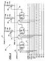
- Substrate 10may include three fluid supply slots 14 , 16 , and 18 therethrough for flow of fluid from an opposite surface of the substrate 10 to a device surface 20 of the substrate 10 .
- Substrate 12may include a single fluid supply slot 22 for flow of fluid from an opposite surface to a device surface 24 of the substrate 12 .
- the device surfaces 20 and 24include a plurality of fluid ejection actuators 26 and 28 disposed in substantially columnar arrays 30 , 32 , and 34 on substrate 10 and in columnar arrays 36 and 38 on substrate 12 .
- the ejection actuators 26are disposed adjacent the fluid supply slots 14 , 16 , and 18 on at least one side thereof as illustrated. However, the ejection actuators may be disposed on both sides of the fluid supply slots 14 , 16 , and 18 .
- the ejection actuators 28are disposed adjacent the fluid supply slot 22 on opposing sides thereof.
- Contact pads 40 and 42are disposed on the surfaces 20 and 24 of the substrates 10 and 12 for electrical connection to a control device for activating the actuators.
- driver and control logicare also included on the device surfaces 20 and 24 of the substrate.
- the control logicincludes power and ground interconnections in a first metal conductor layer.
- the driver logicincludes power transistors 44 and 46 for providing energy to the ejection actuators 26 and 28 respectively. As will be described in more detail below, the power transistors 44 and 46 are connected through the first metal conductor layer to the ejection actuators 26 and 28 .
- the power transistors 44 and 46are included in columnar arrays 48 , 50 , and 52 adjacent the arrays 30 , 32 , and 34 of actuators 26 on the substrate 10 and in columnar arrays 54 and 56 adjacent the arrays 36 and 38 of actuators 28 on substrate 12 .
- Control logic arrays 58 , 60 , and 62are disposed adjacent the power transistors 44 and control logic arrays 64 and 66 are disposed adjacent the power transistors 46 . Interconnection between the control logic arrays 58 - 66 and the power transistors 44 and 46 is in a polysilicon layer rather than in the first metal conductor layer or in a second metal conductor layer thereby eliminating the need for a three metal layer process for providing interconnections and power and ground buss routing to the devices.
- polysilicon interconnectionsare less desirable than metal interconnections due to a higher resistance of the polysilicon interconnections than in metal interconnections. Higher resistance may lead to actuator timing problems particularly with respect to interconnections between the power transistors 44 and 46 and the ejection actuators 26 and 28 .
- embodiments of the disclosurecircumvent such timing problems by using polysilicon interconnections only between the control logic arrays 58 - 66 and the power transistor arrays 48 - 56 .
- FIG. 3A cross-sectional view, not to scale, of a portion of the substrate 10 is illustrated in FIG. 3 .
- the semiconductor substrate 10includes a silicon substrate 68 having a dielectric layer 70 provided between the substrate 68 and device layers on the surface 20 of the substrate 10 .
- a first metal conductor layer 72provides power and ground interconnections for logic devices 76 .
- Ejection actuator 26is preferably a heater resistor provided between anode and cathode conductors 72 A and 72 B ( FIG. 5 ) provided by a first metal conductor layer 72 .
- the first metal conductor layer 72also provides interconnection between the ejection actuator 26 and the power transistor 44 .
- the power transistor 44is a field effect transistor (FET).
- Control logic for the power transistor 44is provided by logic devices 76 which may be interconnected with the power transistor 44 using a polysilicon interconnection layer 78 .
- a second metal conductor layer 74provides a ground buss and a power buss, as described in more detail below, over the P buss, logic devices 76 , address buss, and FET 44 .
- FIG. 4is a schematic diagram of a portion of a circuit 82 for the ejector actuators 26 .
- the first metal conductor layer 72provides power and ground connections to control devices 76 .
- the polysilicon layer 78provides interconnection between address busses P1F1-P1F2, EA0-EA1 and A1-A5 and interconnection between the control devices 76 and the FET's 44 .
- the second metal conductor layer 74provides the power and ground connections to the FET 44 and to the anode and cathode conductors 72 A and 72 B for the ejection actuator 26 .
- the micro-fluid ejection head 84includes the silicon substrate 68 , the dielectric layer 70 , made of silicon dioxide, phosphorus doped glass (PSG) or boron and phosphorus doped glass (BSPG) deposited or grown on the silicon substrate 68 .
- the dielectric layer 70has a thickness ranging from about 8,000 to about 30,000 Angstroms.
- the silicon substrate 12typically has a thickness ranging from about 100 to about 800 microns or more.
- a resistive layer 86is deposited on the dielectric layer 70 .
- the resistive layer 86may be selected from TaAl, Ta 2 N, TaAl(O,N), TaAlSi, TaSiC, Ti(N,O), WSi(O,N), TaAlN and TaAl/Ta and has a thickness ranging from about 500 to about 1,500 Angstroms.
- the first metal conductive layer 72is deposited on the resistive layer 86 and is etched to provide anode and cathode conductors 72 A and 72 B for a heater resistor 26 defined between the anode and cathode conductors 72 A and 72 B.
- the first metal conductive layer 72may be selected from conductive metals, including but not limited to, gold, aluminum, silver, copper, and the like and has a thickness ranging from about 4,000 to about 15,000 Angstroms.
- a passivation layer 88is deposited on the heater resistor 26 and a portion of conductive layer 72 to protect the heater resistor 26 from fluid corrosion.
- the passivation layer 88typically consists of composite layers of silicon nitride (SiN) and silicon carbide (SiC) with SiC being the top layer.
- the passivation layer 88has an overall thickness ranging from about 1,000 to about 8,000 Angstroms.
- a cavitation layer 90is then deposited on the passivation layer 88 overlying the heater resistor 26 .
- the cavitation layer 90has a thickness ranging from about 1,500 to about 8,000 Angstroms and is typically composed of tantalum (Ta).
- the cavitation layer 90also referred to as the “fluid contact layer” provides protection of the heater resistor 26 from erosion due to bubble collapse and mechanical shock during fluid ejection cycles.
- anode and cathode conductors 72 A and 72 BOverlying the anode and cathode conductors 72 A and 72 B is another insulating layer or dielectric layer 92 typically composed of epoxy photoresist materials, polyimide materials, silicon nitride, silicon carbide, silicon dioxide, spun-on-glass (SOG), laminated polymer and the like.
- the layer 92preferably has a thickness ranging from about 5,000 to about 20,000 Angstroms.
- the dielectric layer 92provides electrical insulation between the first metal conductor layer 72 and the second metal conductor layer 74 .
- a nozzle plate 94 containing nozzle holes 96 , fluid chambers 98 , fluid flow channels 100are formed in the nozzle plate 94 .
- the fluid chambers 98 and fluid flow channels 100are in flow communication with the fluid supply slot 14 , 16 , or 18 .
- the nozzle plate 94is adhesively attached to the device surface 20 of the substrate 10 as by means of adhesive 102 .
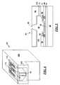
- a fluid supply cartridge 104 containing the ejection head 84is illustrated in FIG. 6 .
- the micro-fluid ejection head 84is attached to an ejection head portion 106 of the fluid cartridge 104 .
- a main body 108 of the cartridge 104includes a fluid reservoir for supply of fluid to the micro-fluid ejection head structure 84 .
- a flexible circuit or tape automated bonding (TAB) circuit 110 containing electrical contacts 112 for connection to a control device such as the printeris attached to the main body 108 of the cartridge 104 .
- Electrical tracing 114 from the electrical contacts 112are attached to the contact pads 40 ( FIG. 1 ) on the substrate 10 to provide activation of the ejection actuators 26 on demand from the control device to which the fluid cartridge 104 is attached.
- TABtape automated bonding
- the disclosureis not limited to the fluid cartridge 104 described above as the micro-fluid ejection head 84 may be used in a wide variety of fluid cartridges, wherein the ejection head 84 may be remote from the fluid reservoir of the main body 108 .
- the first metal conductor layer 72 and the second metal conductor layer 74there are two metal conductor layers, i.e., the first metal conductor layer 72 and the second metal conductor layer 74 , and a polysilicon layer 78 providing interconnection between the ejection actuators 26 , power transistor 44 and device logic 76 on the surface 20 of the substrate 10 .
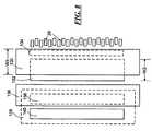
- the second metal conductor layer 74provided power busses 120 and the first metal conductor layer 72 provided the ground buss 122 as illustrated in FIG. 7 .
- the power buss 120is disposed over a portion of an active area 124 of the columnar array of power transistors 48 , 50 , or 52 ( FIG. 1 ).
- the ground buss 122is also routed over a portion of the active area 124 of the columnar array of power transistors 48 , 50 , or 52 .
- the active area 124has a width W 1 ranging from about 400 to about 1000 microns.
- Area 128 in FIG. 6represents the control logic array 58 , 60 , or 62 ( FIG. 1 ).
- the overall width WS of the substrate 10ranges from about three millimeters to about six millimeters in order to provide surface 20 sufficient for the ejection actuator arrays 30 , 32 , or 34 , power transistor arrays 48 , 50 , or 52 and control logic arrays 58 , 60 , or 62 as well as contact pads 40 and conductor routing for the power and ground busses 120 and 122 .
- substrate 12FIG. 2 ).
- the size of the power transistors 44 or 46is reduced.
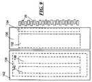
- the power and ground bussesmay be routed as illustrated in FIGS. 8 and 9 .
- a power buss 130is routed over at least a portion of an active area 132 for the power transistor array 48 , 50 , or 52 .
- the active area 132has a width W 2 ranging from about 50 to about 400 microns.
- the power buss 130may also overly a columnar array 134 of temperature sense resistors (TSR) disposed between the fluid ejection devices 26 and the active area 132 of the power transistor array 48 , 50 , or 52 .
- TSRtemperature sense resistors
- the ground buss 136is disposed adjacent the power buss 130 in the second metal conductive layer 74 , however, the ground buss 136 overlies at least a portion of the control logic area 128 .
- the control logic area 128may include active capacitors, arrays of select logic cells (predrive) 138 that select the gate of the power transistors 44 to activate the ejection devices 26 , primitive (P), address (A), and extended address (EA) buss lines, control buss lines, pdata register arrays 140 , and the like.
- the overall width WS of the substrate 10may be made smaller provided the power and ground busses 130 and 136 in the second metal conductive layer 74 are made to overly the active area 132 and control logic area 128 as shown in FIG. 8 .
- power buss 130overlies the active area 132 of the power transistors 48 , 50 , or 52 and overlies the columnar array 134 of temperature sense resistors (TSR).
- TSRtemperature sense resistors
- a larger ground buss 142overlies the control logic area 128 .
- One of the unique aspects of the foregoing embodimentsis the ability to route the ground buss 136 or a ground buss 142 over all or a portion of the control logic area 128 for the power transistors 44 while still using only two metal conductor layers 72 and 74 as described above. Such aspects may be achieved by carefully routing the control logic arrays 58 , 60 , or 62 only in the first metal conductor layer 72 using the polysilicon interconnections 78 between the control logic arrays 58 , 60 , and 62 and the power transistor arrays 48 , 50 , or 52 . Since only the control logic interconnections 78 are routed in polysilicon, there may be no noticeable adverse pulse timing effect for firing the ejection actuators 26 . Use of polysilicon interconnections 78 enables an increase in area that may be used for routing the ground and power busses in the second metal conductor layer 74 .
- Another unique aspect of the disclosed embodimentsis the use of a non-metal TSR material for the TSR arrays 134 thus enabling the power buss 130 to be routed in the second metal conductor layer 74 over the TSR arrays 134 . Accordingly, all conductor routing is in no more than two metal conductor layers.
Landscapes
- Particle Formation And Scattering Control In Inkjet Printers (AREA)
- Semiconductor Integrated Circuits (AREA)
Abstract
Description
- The disclosure relates to micro-fluid ejection head substrates and in particular to improved conductor layouts for reduced substrate size.
- Micro-fluid ejection devices continue to be used in a wide variety of applications, including ink jet printers, medical delivery devices, micro-coolers and the like. Of the uses, ink jet printers provide, by far, the most common use of micro-fluid ejection devices. Ink jet printers are typically more versatile than laser printers for some applications. As the capabilities of ink jet printers are increased to provide higher quality images at increased printing rates, fluid ejection heads, which are the primary printing components of ink jet printers, continue to evolve and become more complex.
- As the complexity of micro-fluid ejection devices increases, there is a need to include more functions on semiconductor substrates for the devices. However, there is a competing need to maintain or reduce the size of the substrates so as to minimize the cost of the ejection devices. While miniaturization provides benefits relative to material costs, such miniaturization may also have negative effects on operational properties of the devices. For example, reducing the size of ground and power busses on the substrate may enable smaller size substrates to be used. However, reduced size busses usually have higher resistance and thus generate more heat than larger busses. Hence, there continues to be a need for improved substrate conductor routing and layouts that do not adversely affect the electrical properties of the circuits.
- With regard to the above and other objects and advantages, the disclosure provides a semiconductor substrate for a micro-fluid ejection device. The substrate includes plurality of micro-fluid ejection actuators disposed in a columnar array adjacent a fluid supply slot in the semiconductor substrate. A plurality of power transistors are disposed in a columnar array adjacent the ejection actuators and are connected through a first metal conductor layer to the ejection actuators. The columnar array of power transistors occupies a power transistor active area of the substrate. A columnar array of logic circuits is disposed adjacent the columnar array of power transistors and is connected through a polysilicon conductor layer to the power transistors. The columnar array of logic circuits occupies a logic circuit area of the substrate. A power conductor for the ejection actuators is routed in a second metal conductor layer and is disposed in overlapping relationship with at least a portion of the power transistor active area of the substrate. A ground conductor for the ejection actuators is routed in the second metal conductor layer and is disposed in overlapping relationship with at least a portion of the logic circuit area of the substrate.
- In another embodiment, there is provided a method for reducing a width of a semiconductor substrate for a micro-fluid ejection device. The method includes providing at least one fluid supply slot in a semiconductor substrate. A plurality of micro-fluid ejection actuators are in a columnar array on a device surface of a semiconductor substrate adjacent the fluid supply slot. A plurality of power transistors are formed in a columnar array adjacent the ejection actuators. The power transistors occupy a power transistor area of the substrate and are interconnected to the ejection actuators in a first metal conductor layer. A columnar array of logic circuits are formed adjacent the power transistors. The logic circuits occupy a logic circuit area of the substrate and are interconnected to the power transistors in a polysilicon conductor layer. A second metal layer is deposited on the semiconductor substrate to provide a power buss and a ground buss to the ejection actuators. The power buss overlaps at least a portion of the power transistor active area and the ground buss overlaps at least a portion of the logic circuit area.
- An advantage of the embodiments of the disclosure is that it provides suitably sized power and ground buss conductors for components on a semiconductor substrate without the need to increase the size of the substrate or surface area available for routing the power and ground busses. For example, the power and ground buss conductors may be provided with a size that does not adversely affect resistance values of the conductors to fluid ejection actuators on the substrate thereby providing more energy to the fluid ejection actuators. Another advantage of the embodiments is that it provides polysilicon interconnections between selected components without adversely affecting the timing of firing pulses for the fluid ejection actuators.
- Further advantages of the disclosed embodiments will become apparent by reference to the detailed description of preferred embodiments when considered in conjunction with the following drawings illustrating one or more non-limiting aspects of the embodiments, wherein like reference characters designate like or similar elements throughout the several drawings as follows:
FIGS. 1 and 2 are plan views, not to scale, of semiconductor substrates for micro-fluid ejection heads according to the disclosure;FIG. 3 is a cross-sectional view, not to scale, of a portion of a semiconductor substrate for a micro-fluid ejection head;FIG. 4 is a schematic diagram of a portion of a circuit for a micro-fluid ejection head according to the disclosure;FIG. 5 is a cross-sectional view, not to scale, of a portion of a micro-fluid ejection head according to the disclosure;FIG. 6 is a perspective view, not to scale, of a cartridge containing a micro-fluid ejection head according to the disclosure;FIG. 7 is a block diagram of a plan view of a prior art semiconductor substrate; andFIGS. 8 and 9 are block diagrams of plan views of semiconductor substrates according to embodiments of the disclosure.- With reference to
FIGS. 1 and 2 , embodiments of the disclosure provide improvedsemiconductor substrates Substrate 10, for example, may include threefluid supply slots substrate 10 to adevice surface 20 of thesubstrate 10.Substrate 12 may include a single fluid supply slot22 for flow of fluid from an opposite surface to adevice surface 24 of thesubstrate 12. Thedevice surfaces fluid ejection actuators 26 and28 disposed in substantiallycolumnar arrays substrate 10 and incolumnar arrays substrate 12. Forsubstrate 10, theejection actuators 26 are disposed adjacent thefluid supply slots fluid supply slots - For
substrate 12, the ejection actuators28 are disposed adjacent the fluid supply slot22 on opposing sides thereof.Contact pads surfaces substrates - In order to selectively activate certain ones of the
ejection actuators 26 or28, driver and control logic are also included on thedevice surfaces power transistors 44 and46 for providing energy to theejection actuators 26 and28 respectively. As will be described in more detail below, thepower transistors 44 and46 are connected through the first metal conductor layer to theejection actuators 26 and28. Like theejection actuators 26 and28, thepower transistors 44 and46 are included incolumnar arrays arrays actuators 26 on thesubstrate 10 and incolumnar arrays 54 and56 adjacent thearrays substrate 12. Control logic arrays power transistors 44 andcontrol logic arrays power transistors 44 and46 is in a polysilicon layer rather than in the first metal conductor layer or in a second metal conductor layer thereby eliminating the need for a three metal layer process for providing interconnections and power and ground buss routing to the devices.- In general, polysilicon interconnections are less desirable than metal interconnections due to a higher resistance of the polysilicon interconnections than in metal interconnections. Higher resistance may lead to actuator timing problems particularly with respect to interconnections between the
power transistors 44 and46 and theejection actuators 26 and28. However, embodiments of the disclosure circumvent such timing problems by using polysilicon interconnections only between the control logic arrays58-66 and the power transistor arrays48-56. - A cross-sectional view, not to scale, of a portion of the
substrate 10 is illustrated inFIG. 3 . As illustrated inFIG. 3 , thesemiconductor substrate 10 includes asilicon substrate 68 having adielectric layer 70 provided between thesubstrate 68 and device layers on thesurface 20 of thesubstrate 10. A firstmetal conductor layer 72 provides power and ground interconnections forlogic devices 76.Ejection actuator 26 is preferably a heater resistor provided between anode andcathode conductors FIG. 5 ) provided by a firstmetal conductor layer 72. The firstmetal conductor layer 72 also provides interconnection between theejection actuator 26 and thepower transistor 44. In the illustration ofFIG. 3 , thepower transistor 44 is a field effect transistor (FET). Control logic for thepower transistor 44 is provided bylogic devices 76 which may be interconnected with thepower transistor 44 using apolysilicon interconnection layer 78. A secondmetal conductor layer 74 provides a ground buss and a power buss, as described in more detail below, over the P buss,logic devices 76, address buss, andFET 44. FIG. 4 is a schematic diagram of a portion of acircuit 82 for theejector actuators 26. As shown inFIG. 4 , the firstmetal conductor layer 72 provides power and ground connections to controldevices 76. Thepolysilicon layer 78 provides interconnection between address busses P1F1-P1F2, EA0-EA1 and A1-A5 and interconnection between thecontrol devices 76 and the FET's44. The secondmetal conductor layer 74 provides the power and ground connections to theFET 44 and to the anode andcathode conductors ejection actuator 26.- A portion of a
micro-fluid ejection head 84 is illustrated inFIG. 5 . Themicro-fluid ejection head 84 includes thesilicon substrate 68, thedielectric layer 70, made of silicon dioxide, phosphorus doped glass (PSG) or boron and phosphorus doped glass (BSPG) deposited or grown on thesilicon substrate 68. Thedielectric layer 70 has a thickness ranging from about 8,000 to about 30,000 Angstroms. Thesilicon substrate 12 typically has a thickness ranging from about 100 to about 800 microns or more. - A
resistive layer 86 is deposited on thedielectric layer 70. Theresistive layer 86 may be selected from TaAl, Ta2N, TaAl(O,N), TaAlSi, TaSiC, Ti(N,O), WSi(O,N), TaAlN and TaAl/Ta and has a thickness ranging from about 500 to about 1,500 Angstroms. - The first
metal conductive layer 72 is deposited on theresistive layer 86 and is etched to provide anode andcathode conductors heater resistor 26 defined between the anode andcathode conductors metal conductive layer 72 may be selected from conductive metals, including but not limited to, gold, aluminum, silver, copper, and the like and has a thickness ranging from about 4,000 to about 15,000 Angstroms. - A
passivation layer 88 is deposited on theheater resistor 26 and a portion ofconductive layer 72 to protect theheater resistor 26 from fluid corrosion. Thepassivation layer 88 typically consists of composite layers of silicon nitride (SiN) and silicon carbide (SiC) with SiC being the top layer. Thepassivation layer 88 has an overall thickness ranging from about 1,000 to about 8,000 Angstroms. - A
cavitation layer 90 is then deposited on thepassivation layer 88 overlying theheater resistor 26. Thecavitation layer 90 has a thickness ranging from about 1,500 to about 8,000 Angstroms and is typically composed of tantalum (Ta). Thecavitation layer 90, also referred to as the “fluid contact layer” provides protection of theheater resistor 26 from erosion due to bubble collapse and mechanical shock during fluid ejection cycles. - Overlying the anode and
cathode conductors dielectric layer 92 typically composed of epoxy photoresist materials, polyimide materials, silicon nitride, silicon carbide, silicon dioxide, spun-on-glass (SOG), laminated polymer and the like. Thelayer 92 preferably has a thickness ranging from about 5,000 to about 20,000 Angstroms. Thedielectric layer 92 provides electrical insulation between the firstmetal conductor layer 72 and the secondmetal conductor layer 74. - In
FIG. 5 , anozzle plate 94 containing nozzle holes96,fluid chambers 98,fluid flow channels 100 are formed in thenozzle plate 94. Thefluid chambers 98 andfluid flow channels 100 are in flow communication with thefluid supply slot nozzle plate 94 is adhesively attached to thedevice surface 20 of thesubstrate 10 as by means of adhesive102. - A
fluid supply cartridge 104 containing theejection head 84 is illustrated inFIG. 6 . Themicro-fluid ejection head 84 is attached to anejection head portion 106 of thefluid cartridge 104. Amain body 108 of thecartridge 104 includes a fluid reservoir for supply of fluid to the micro-fluidejection head structure 84. A flexible circuit or tape automated bonding (TAB)circuit 110 containingelectrical contacts 112 for connection to a control device such as the printer is attached to themain body 108 of thecartridge 104. Electrical tracing114 from theelectrical contacts 112 are attached to the contact pads40 (FIG. 1 ) on thesubstrate 10 to provide activation of theejection actuators 26 on demand from the control device to which thefluid cartridge 104 is attached. The disclosure, however, is not limited to thefluid cartridge 104 described above as themicro-fluid ejection head 84 may be used in a wide variety of fluid cartridges, wherein theejection head 84 may be remote from the fluid reservoir of themain body 108. - As set forth above, there are two metal conductor layers, i.e., the first
metal conductor layer 72 and the secondmetal conductor layer 74, and apolysilicon layer 78 providing interconnection between theejection actuators 26,power transistor 44 anddevice logic 76 on thesurface 20 of thesubstrate 10. In a prior art design, the secondmetal conductor layer 74 providedpower busses 120 and the firstmetal conductor layer 72 provided theground buss 122 as illustrated inFIG. 7 . - In the prior art design shown in
FIG. 7 , thepower buss 120 is disposed over a portion of anactive area 124 of the columnar array ofpower transistors FIG. 1 ). Theground buss 122 is also routed over a portion of theactive area 124 of the columnar array ofpower transistors - In this case, the
active area 124 has a width W1 ranging from about 400 to about 1000 microns.Area 128 inFIG. 6 represents thecontrol logic array FIG. 1 ). Accordingly, the overall width WS of thesubstrate 10 ranges from about three millimeters to about six millimeters in order to providesurface 20 sufficient for theejection actuator arrays power transistor arrays control logic arrays contact pads 40 and conductor routing for the power and ground busses120 and122. The foregoing description also applies to substrate12 (FIG. 2 ). - As the resistance of the
ejection actuators 26 increases for improved micro-fluid ejection heads84, the size of thepower transistors 44 or46 is reduced. In order to provide sufficiently sized metal conductors for the power and ground busses without increasing the width WS of thesubstrate 10, the power and ground busses may be routed as illustrated inFIGS. 8 and 9 . InFIG. 8 , apower buss 130 is routed over at least a portion of anactive area 132 for thepower transistor array active area 132 has a width W2 ranging from about 50 to about 400 microns. In order to increase a width W3 of thepower buss 130 in the secondmetal conductive layer 74, thepower buss 130 may also overly acolumnar array 134 of temperature sense resistors (TSR) disposed between thefluid ejection devices 26 and theactive area 132 of thepower transistor array - In the embodiment illustrated in
FIG. 8 , theground buss 136 is disposed adjacent thepower buss 130 in the secondmetal conductive layer 74, however, theground buss 136 overlies at least a portion of thecontrol logic area 128. For example, thecontrol logic area 128 may include active capacitors, arrays of select logic cells (predrive)138 that select the gate of thepower transistors 44 to activate theejection devices 26, primitive (P), address (A), and extended address (EA) buss lines, control buss lines,pdata register arrays 140, and the like. - It will be appreciated that since the width W2 of the
active area 132 of thepower transistor array FIG. 8 ), the overall width WS of thesubstrate 10 may be made smaller provided the power and ground busses130 and136 in the secondmetal conductive layer 74 are made to overly theactive area 132 and controllogic area 128 as shown inFIG. 8 . - In an alternative embodiment, illustrated in
FIG. 9 ,power buss 130 overlies theactive area 132 of thepower transistors columnar array 134 of temperature sense resistors (TSR). Alarger ground buss 142 overlies thecontrol logic area 128. - One of the unique aspects of the foregoing embodiments is the ability to route the
ground buss 136 or aground buss 142 over all or a portion of thecontrol logic area 128 for thepower transistors 44 while still using only two metal conductor layers72 and74 as described above. Such aspects may be achieved by carefully routing thecontrol logic arrays metal conductor layer 72 using thepolysilicon interconnections 78 between thecontrol logic arrays power transistor arrays control logic interconnections 78 are routed in polysilicon, there may be no noticeable adverse pulse timing effect for firing theejection actuators 26. Use ofpolysilicon interconnections 78 enables an increase in area that may be used for routing the ground and power busses in the secondmetal conductor layer 74. - Another unique aspect of the disclosed embodiments is the use of a non-metal TSR material for the
TSR arrays 134 thus enabling thepower buss 130 to be routed in the secondmetal conductor layer 74 over theTSR arrays 134. Accordingly, all conductor routing is in no more than two metal conductor layers. - It is contemplated, and will be apparent to those skilled in the art from the preceding description and the accompanying drawings, that modifications and changes may be made in the embodiments of the disclosure. Accordingly, it is expressly intended that the foregoing description and the accompanying drawings are illustrative of preferred embodiments only, not limiting thereto, and that the true spirit and scope of the present disclosure be determined by reference to the appended claims.
Claims (17)
Priority Applications (2)
| Application Number | Priority Date | Filing Date | Title |
|---|---|---|---|
| US10/956,939US7195341B2 (en) | 2004-09-30 | 2004-09-30 | Power and ground buss layout for reduced substrate size |
| US11/676,551US7344227B2 (en) | 2004-09-30 | 2007-02-20 | Power and ground buss layout for reduced substrate size |
Applications Claiming Priority (1)
| Application Number | Priority Date | Filing Date | Title |
|---|---|---|---|
| US10/956,939US7195341B2 (en) | 2004-09-30 | 2004-09-30 | Power and ground buss layout for reduced substrate size |
Related Child Applications (1)
| Application Number | Title | Priority Date | Filing Date |
|---|---|---|---|
| US11/676,551DivisionUS7344227B2 (en) | 2004-09-30 | 2007-02-20 | Power and ground buss layout for reduced substrate size |
Publications (2)
| Publication Number | Publication Date |
|---|---|
| US20060066681A1true US20060066681A1 (en) | 2006-03-30 |
| US7195341B2 US7195341B2 (en) | 2007-03-27 |
Family
ID=36098540
Family Applications (2)
| Application Number | Title | Priority Date | Filing Date |
|---|---|---|---|
| US10/956,939Expired - LifetimeUS7195341B2 (en) | 2004-09-30 | 2004-09-30 | Power and ground buss layout for reduced substrate size |
| US11/676,551Expired - LifetimeUS7344227B2 (en) | 2004-09-30 | 2007-02-20 | Power and ground buss layout for reduced substrate size |
Family Applications After (1)
| Application Number | Title | Priority Date | Filing Date |
|---|---|---|---|
| US11/676,551Expired - LifetimeUS7344227B2 (en) | 2004-09-30 | 2007-02-20 | Power and ground buss layout for reduced substrate size |
Country Status (1)
| Country | Link |
|---|---|
| US (2) | US7195341B2 (en) |
Cited By (7)
| Publication number | Priority date | Publication date | Assignee | Title |
|---|---|---|---|---|
| WO2014051540A1 (en)* | 2012-09-25 | 2014-04-03 | Hewlett-Packard Development Company, L.P. | Print head die with thermal control |
| WO2015080709A1 (en)* | 2013-11-26 | 2015-06-04 | Hewlett-Packard Development Company, Lp | Fluid ejection apparatus with single-side thermal sensor |
| CN107000440A (en)* | 2014-12-02 | 2017-08-01 | 惠普发展公司,有限责任合伙企业 | Print Head |
| CN110624614A (en)* | 2014-12-08 | 2019-12-31 | 伯克利之光生命科技公司 | Microfluidic devices comprising lateral/vertical transistor structures and methods of making and using the same |
| CN113396065A (en)* | 2019-02-06 | 2021-09-14 | 惠普发展公司,有限责任合伙企业 | Die for printhead |
| US11613118B2 (en) | 2019-02-06 | 2023-03-28 | Hewlett-Packard Development Company, L.P. | Die for a printhead |
| US11642884B2 (en) | 2019-02-06 | 2023-05-09 | Hewlett-Packard Development Company, L.P. | Die for a printhead |
Families Citing this family (10)
| Publication number | Priority date | Publication date | Assignee | Title |
|---|---|---|---|---|
| US7465041B2 (en)* | 2005-10-11 | 2008-12-16 | Silverbrook Research Pty Ltd | Inkjet printhead with inlet priming feature |
| US8622524B2 (en) | 2010-05-27 | 2014-01-07 | Funai Electric Co., Ltd. | Laminate constructs for micro-fluid ejection devices |
| CN102689513B (en)* | 2011-03-23 | 2015-02-18 | 研能科技股份有限公司 | Inkjet head structure |
| US8444255B2 (en) | 2011-05-18 | 2013-05-21 | Hewlett-Packard Development Company, L.P. | Power distribution in a thermal ink jet printhead |
| CA2932092C (en) | 2013-11-27 | 2018-05-01 | Hewlett-Packard Development Company, Lp | Fluid ejection apparatus with single power supply connector |
| US9259754B2 (en) | 2014-06-20 | 2016-02-16 | Stmicroelectronics Asia Pacific Pte Ltd | Microfluidic delivery member with filter and method of forming same |
| US10264667B2 (en)* | 2014-06-20 | 2019-04-16 | Stmicroelectronics, Inc. | Microfluidic delivery system with a die on a rigid substrate |
| BR112017002973B1 (en) | 2014-08-18 | 2022-04-12 | Hewlett-Packard Development Company, L.P. | print head matrix |
| US11975534B2 (en) | 2017-07-11 | 2024-05-07 | Hewlett-Packard Development Company, L.P. | Fluid actuator evaluation based on actuator activation data |
| EP3720720A4 (en)* | 2017-12-08 | 2021-07-21 | Hewlett-Packard Development Company, L.P. | Gaps between electrically conductive ground structures |
Citations (32)
| Publication number | Priority date | Publication date | Assignee | Title |
|---|---|---|---|---|
| US4458256A (en)* | 1979-03-06 | 1984-07-03 | Canon Kabushiki Kaisha | Ink jet recording apparatus |
| US4935752A (en)* | 1989-03-30 | 1990-06-19 | Xerox Corporation | Thermal ink jet device with improved heating elements |
| US4985710A (en)* | 1989-11-29 | 1991-01-15 | Xerox Corporation | Buttable subunits for pagewidth "Roofshooter" printheads |
| US5030971A (en)* | 1989-11-29 | 1991-07-09 | Xerox Corporation | Precisely aligned, mono- or multi-color, `roofshooter` type printhead |
| US5144341A (en)* | 1991-04-26 | 1992-09-01 | Xerox Corporation | Thermal ink jet drivers device design/layout |
| US5159353A (en)* | 1991-07-02 | 1992-10-27 | Hewlett-Packard Company | Thermal inkjet printhead structure and method for making the same |
| US5469199A (en)* | 1990-08-16 | 1995-11-21 | Hewlett-Packard Company | Wide inkjet printhead |
| US5600354A (en)* | 1992-04-02 | 1997-02-04 | Hewlett-Packard Company | Wrap-around flex with address and data bus |
| US5635966A (en)* | 1994-01-11 | 1997-06-03 | Hewlett-Packard Company | Edge feed ink delivery thermal inkjet printhead structure and method of fabrication |
| US5644342A (en)* | 1993-03-31 | 1997-07-01 | Hewlett-Packard Company | Addressing system for an integrated printhead |
| US5666142A (en)* | 1990-01-31 | 1997-09-09 | Canon Kabushiki Kaisha | Ink jet recording system having improved functional devices for driving energy generating members |
| US5835112A (en)* | 1996-10-08 | 1998-11-10 | Hewlett-Packard Company | Segmented electrical distribution plane |
| US5883650A (en)* | 1995-12-06 | 1999-03-16 | Hewlett-Packard Company | Thin-film printhead device for an ink-jet printer |
| US5887098A (en)* | 1997-02-27 | 1999-03-23 | Molex Incorporated | Fiber optic adapter with protective shield |
| US5933161A (en)* | 1996-03-21 | 1999-08-03 | Fuji Xerox Co., Ltd. | Ink-jet recorder having a driving circuit for driving heat-generating elements |
| US6019907A (en)* | 1997-08-08 | 2000-02-01 | Hewlett-Packard Company | Forming refill for monolithic inkjet printhead |
| US6227657B1 (en)* | 2000-06-19 | 2001-05-08 | Xerox Corporation | Low topography thermal inkjet drop ejector structure |
| US6239820B1 (en)* | 1995-12-06 | 2001-05-29 | Hewlett-Packard Company | Thin-film printhead device for an ink-jet printer |
| US6305790B1 (en)* | 1996-02-07 | 2001-10-23 | Hewlett-Packard Company | Fully integrated thermal inkjet printhead having multiple ink feed holes per nozzle |
| US6309053B1 (en)* | 2000-07-24 | 2001-10-30 | Hewlett-Packard Company | Ink jet printhead having a ground bus that overlaps transistor active regions |
| US20020020921A1 (en)* | 1998-05-19 | 2002-02-21 | Chieh-Wen Wang | Structure of an ink-jet printhead chip and manufacturing method thereof |
| US6350017B1 (en)* | 1999-05-31 | 2002-02-26 | Casio Computer Co., Ltd. | Ink-jet printer head and manufacturing method thereof |
| US6402302B1 (en)* | 1999-06-04 | 2002-06-11 | Canon Kabushiki Kaisha | Liquid discharge head, manufacturing method thereof, and microelectromechanical device |
| US6422676B1 (en)* | 2001-06-19 | 2002-07-23 | Hewlett-Packard Company | Compact ink jet printhead |
| US20030011658A1 (en)* | 2001-04-12 | 2003-01-16 | Parish George Keith | Power distribution architecture for inkjet heater chip |
| US6543883B1 (en)* | 2001-09-29 | 2003-04-08 | Hewlett-Packard Company | Fluid ejection device with drive circuitry proximate to heating element |
| US6554404B2 (en)* | 1996-02-07 | 2003-04-29 | Hewlett-Packard Development Company, L.P. | Conductor routing for a printhead |
| US6565175B1 (en)* | 1999-07-12 | 2003-05-20 | Olivetti Tecnost S.P.A. | Integrated printhead |
| US6575562B1 (en)* | 1999-11-16 | 2003-06-10 | Lexmark International, Inc. | Performance inkjet printhead chip layouts and assemblies |
| US20030107616A1 (en)* | 2001-11-08 | 2003-06-12 | Tsung-Wei Huang | Fluid injection head structure and method for manufacturing the same |
| US20030210301A1 (en)* | 2002-05-08 | 2003-11-13 | Xerox Corporation | Polysilicon feed-through fluid drop ejector |
| US6726311B2 (en)* | 2001-01-30 | 2004-04-27 | Hewlett-Packard Development Company, L.P. | Energy balanced printhead design |
Family Cites Families (4)
| Publication number | Priority date | Publication date | Assignee | Title |
|---|---|---|---|---|
| EP0317171A3 (en) | 1987-11-13 | 1990-07-18 | Hewlett-Packard Company | Integral thin film injection system for thermal ink jet heads and methods of operation |
| US4887098A (en) | 1988-11-25 | 1989-12-12 | Xerox Corporation | Thermal ink jet printer having printhead transducers with multilevelinterconnections |
| US6200407B1 (en)* | 1994-08-18 | 2001-03-13 | Rockwell Technologies, Llc | Method of making a multilayer circuit board having a window exposing an enhanced conductive layer for use as an insulated mounting area |
| US20020071293A1 (en)* | 2000-07-13 | 2002-06-13 | Eden Richard C. | Power semiconductor switching devices, power converters, integrated circuit assemblies, integrated circuitry, power current switching methods, methods of forming a power semiconductor switching device, power conversion methods, power semiconductor switching device packaging methods, and methods a of forming power transistor |
- 2004
- 2004-09-30USUS10/956,939patent/US7195341B2/ennot_activeExpired - Lifetime
- 2007
- 2007-02-20USUS11/676,551patent/US7344227B2/ennot_activeExpired - Lifetime
Patent Citations (35)
| Publication number | Priority date | Publication date | Assignee | Title |
|---|---|---|---|---|
| US4458256A (en)* | 1979-03-06 | 1984-07-03 | Canon Kabushiki Kaisha | Ink jet recording apparatus |
| US4935752A (en)* | 1989-03-30 | 1990-06-19 | Xerox Corporation | Thermal ink jet device with improved heating elements |
| US4985710A (en)* | 1989-11-29 | 1991-01-15 | Xerox Corporation | Buttable subunits for pagewidth "Roofshooter" printheads |
| US5030971A (en)* | 1989-11-29 | 1991-07-09 | Xerox Corporation | Precisely aligned, mono- or multi-color, `roofshooter` type printhead |
| US5030971B1 (en)* | 1989-11-29 | 2000-11-28 | Xerox Corp | Precisely aligned mono- or multi-color roofshooter type printhead |
| US5666142A (en)* | 1990-01-31 | 1997-09-09 | Canon Kabushiki Kaisha | Ink jet recording system having improved functional devices for driving energy generating members |
| US5469199A (en)* | 1990-08-16 | 1995-11-21 | Hewlett-Packard Company | Wide inkjet printhead |
| US5144341A (en)* | 1991-04-26 | 1992-09-01 | Xerox Corporation | Thermal ink jet drivers device design/layout |
| US5159353A (en)* | 1991-07-02 | 1992-10-27 | Hewlett-Packard Company | Thermal inkjet printhead structure and method for making the same |
| US5600354A (en)* | 1992-04-02 | 1997-02-04 | Hewlett-Packard Company | Wrap-around flex with address and data bus |
| US5644342A (en)* | 1993-03-31 | 1997-07-01 | Hewlett-Packard Company | Addressing system for an integrated printhead |
| US5635966A (en)* | 1994-01-11 | 1997-06-03 | Hewlett-Packard Company | Edge feed ink delivery thermal inkjet printhead structure and method of fabrication |
| US6153114A (en)* | 1995-12-06 | 2000-11-28 | Hewlett-Packard Company | Thin-film printhead device for an ink-jet printer |
| US6239820B1 (en)* | 1995-12-06 | 2001-05-29 | Hewlett-Packard Company | Thin-film printhead device for an ink-jet printer |
| US5883650A (en)* | 1995-12-06 | 1999-03-16 | Hewlett-Packard Company | Thin-film printhead device for an ink-jet printer |
| US6554404B2 (en)* | 1996-02-07 | 2003-04-29 | Hewlett-Packard Development Company, L.P. | Conductor routing for a printhead |
| US6305790B1 (en)* | 1996-02-07 | 2001-10-23 | Hewlett-Packard Company | Fully integrated thermal inkjet printhead having multiple ink feed holes per nozzle |
| US5933161A (en)* | 1996-03-21 | 1999-08-03 | Fuji Xerox Co., Ltd. | Ink-jet recorder having a driving circuit for driving heat-generating elements |
| US5835112A (en)* | 1996-10-08 | 1998-11-10 | Hewlett-Packard Company | Segmented electrical distribution plane |
| US5887098A (en)* | 1997-02-27 | 1999-03-23 | Molex Incorporated | Fiber optic adapter with protective shield |
| US6019907A (en)* | 1997-08-08 | 2000-02-01 | Hewlett-Packard Company | Forming refill for monolithic inkjet printhead |
| US20020020921A1 (en)* | 1998-05-19 | 2002-02-21 | Chieh-Wen Wang | Structure of an ink-jet printhead chip and manufacturing method thereof |
| US20020048943A1 (en)* | 1998-05-19 | 2002-04-25 | Chieh-Wen Wang | Structure of an ink-jet printhead chip and manufacturing method thereof |
| US6350017B1 (en)* | 1999-05-31 | 2002-02-26 | Casio Computer Co., Ltd. | Ink-jet printer head and manufacturing method thereof |
| US6402302B1 (en)* | 1999-06-04 | 2002-06-11 | Canon Kabushiki Kaisha | Liquid discharge head, manufacturing method thereof, and microelectromechanical device |
| US6565175B1 (en)* | 1999-07-12 | 2003-05-20 | Olivetti Tecnost S.P.A. | Integrated printhead |
| US6575562B1 (en)* | 1999-11-16 | 2003-06-10 | Lexmark International, Inc. | Performance inkjet printhead chip layouts and assemblies |
| US6227657B1 (en)* | 2000-06-19 | 2001-05-08 | Xerox Corporation | Low topography thermal inkjet drop ejector structure |
| US6309053B1 (en)* | 2000-07-24 | 2001-10-30 | Hewlett-Packard Company | Ink jet printhead having a ground bus that overlaps transistor active regions |
| US6726311B2 (en)* | 2001-01-30 | 2004-04-27 | Hewlett-Packard Development Company, L.P. | Energy balanced printhead design |
| US20030011658A1 (en)* | 2001-04-12 | 2003-01-16 | Parish George Keith | Power distribution architecture for inkjet heater chip |
| US6422676B1 (en)* | 2001-06-19 | 2002-07-23 | Hewlett-Packard Company | Compact ink jet printhead |
| US6543883B1 (en)* | 2001-09-29 | 2003-04-08 | Hewlett-Packard Company | Fluid ejection device with drive circuitry proximate to heating element |
| US20030107616A1 (en)* | 2001-11-08 | 2003-06-12 | Tsung-Wei Huang | Fluid injection head structure and method for manufacturing the same |
| US20030210301A1 (en)* | 2002-05-08 | 2003-11-13 | Xerox Corporation | Polysilicon feed-through fluid drop ejector |
Cited By (20)
| Publication number | Priority date | Publication date | Assignee | Title |
|---|---|---|---|---|
| US9937714B2 (en) | 2012-09-25 | 2018-04-10 | Hewlett-Packard Development Company, L.P. | Print head die with thermal control |
| US9511584B2 (en) | 2012-09-25 | 2016-12-06 | Hewlett-Packard Development Company, L.P. | Print head die with thermal control |
| EP2864123A4 (en)* | 2012-09-25 | 2017-01-11 | Hewlett-Packard Development Company, L.P. | Print head die with thermal control |
| US9676190B2 (en) | 2012-09-25 | 2017-06-13 | Hewlett-Packard Development Company, L.P. | Print head die with thermal control |
| WO2014051540A1 (en)* | 2012-09-25 | 2014-04-03 | Hewlett-Packard Development Company, L.P. | Print head die with thermal control |
| WO2015080709A1 (en)* | 2013-11-26 | 2015-06-04 | Hewlett-Packard Development Company, Lp | Fluid ejection apparatus with single-side thermal sensor |
| US9796178B2 (en) | 2013-11-26 | 2017-10-24 | Hewlett-Packard Development Company, L.P. | Fluid ejection apparatus with single-side thermal sensor |
| CN109466178A (en)* | 2014-12-02 | 2019-03-15 | 惠普发展公司,有限责任合伙企业 | Print head |
| US20170320320A1 (en)* | 2014-12-02 | 2017-11-09 | Hewlett-Packard Development Company, L.P. | Printhead |
| CN107000440B (en)* | 2014-12-02 | 2018-11-06 | 惠普发展公司,有限责任合伙企业 | Print Head |
| CN107000440A (en)* | 2014-12-02 | 2017-08-01 | 惠普发展公司,有限责任合伙企业 | Print Head |
| US10286653B2 (en)* | 2014-12-02 | 2019-05-14 | Hewlett-Packard Development Company, L.P. | Printhead |
| US20190255842A1 (en)* | 2014-12-02 | 2019-08-22 | Hewlett-Packard Development Company, L.P. | Fluid ejection device circuit |
| US10960661B2 (en)* | 2014-12-02 | 2021-03-30 | Hewlett-Packard Development Company, L.P. | Fluid ejection device circuit |
| CN110624614A (en)* | 2014-12-08 | 2019-12-31 | 伯克利之光生命科技公司 | Microfluidic devices comprising lateral/vertical transistor structures and methods of making and using the same |
| US11596941B2 (en) | 2014-12-08 | 2023-03-07 | Berkeley Lights, Inc. | Lateral/vertical transistor structures and process of making and using same |
| CN113396065A (en)* | 2019-02-06 | 2021-09-14 | 惠普发展公司,有限责任合伙企业 | Die for printhead |
| US11413864B2 (en) | 2019-02-06 | 2022-08-16 | Hewlett-Packard Development Company, L.P. | Die for a printhead |
| US11613118B2 (en) | 2019-02-06 | 2023-03-28 | Hewlett-Packard Development Company, L.P. | Die for a printhead |
| US11642884B2 (en) | 2019-02-06 | 2023-05-09 | Hewlett-Packard Development Company, L.P. | Die for a printhead |
Also Published As
| Publication number | Publication date |
|---|---|
| US20070139475A1 (en) | 2007-06-21 |
| US7195341B2 (en) | 2007-03-27 |
| US7344227B2 (en) | 2008-03-18 |
Similar Documents
| Publication | Publication Date | Title |
|---|---|---|
| US7344227B2 (en) | Power and ground buss layout for reduced substrate size | |
| US5635968A (en) | Thermal inkjet printer printhead with offset heater resistors | |
| JP6598658B2 (en) | Element substrate for liquid discharge head and liquid discharge head | |
| US6659597B2 (en) | Liquid discharge head | |
| EP2173560B1 (en) | Printheads | |
| JPH06198885A (en) | Inkjet recording head and monolithic integrated circuit for inkjet recording head | |
| US20060232633A1 (en) | Board for inkjet printing head and inkjet printing head using the same | |
| US9242460B2 (en) | Liquid-discharge-head substrate, method of manufacturing the same, and liquid discharge head | |
| US7441877B2 (en) | Substrate having a plurality of common power supply wires and a plurality of common ground wires for inkjet recording head and inkjet recording head using the same | |
| EP1080903A2 (en) | Shared multiple-terminal ground returns for an ink-jet printhead | |
| JP2004148802A (en) | Inkjet print head | |
| US6938993B2 (en) | Fluid injection head structure | |
| US6981323B2 (en) | Method for fabricating a fluid injection head structure | |
| US6814428B2 (en) | Fluid injection head structure and method thereof | |
| JP2022514711A (en) | Die for printhead | |
| US20180186151A1 (en) | Alternative ground lines for inter-slot grounding | |
| US7810911B2 (en) | Thermal inkjet printhead | |
| KR102621225B1 (en) | Die for printhead | |
| EP4110622B1 (en) | A thermal inkjet printhead, and a printing assembly and printing apparatus comprising the same | |
| EP1568498B1 (en) | Fluid ejection device metal layer layouts | |
| US20250196496A1 (en) | Element substrate and liquid ejection head | |
| US12064965B2 (en) | Element substrate and print head | |
| JPH06238901A (en) | Ink jet recording device | |
| KR20060006657A (en) | Inkjet printhead and how to manufacture it | |
| JP2000015817A (en) | Inkjet head |
Legal Events
| Date | Code | Title | Description |
|---|---|---|---|
| AS | Assignment | Owner name:LEXMARK INTERNATIONAL, INC., KENTUCKY Free format text:ASSIGNMENT OF ASSIGNORS INTEREST;ASSIGNORS:KING, DAVID G.;ROWE, KRISTI M.;REEL/FRAME:015869/0340 Effective date:20040930 | |
| STCF | Information on status: patent grant | Free format text:PATENTED CASE | |
| FPAY | Fee payment | Year of fee payment:4 | |
| AS | Assignment | Owner name:FUNAI ELECTRIC CO., LTD, JAPAN Free format text:ASSIGNMENT OF ASSIGNORS INTEREST;ASSIGNORS:LEXMARK INTERNATIONAL, INC.;LEXMARK INTERNATIONAL TECHNOLOGY, S.A.;REEL/FRAME:030416/0001 Effective date:20130401 | |
| FPAY | Fee payment | Year of fee payment:8 | |
| MAFP | Maintenance fee payment | Free format text:PAYMENT OF MAINTENANCE FEE, 12TH YEAR, LARGE ENTITY (ORIGINAL EVENT CODE: M1553); ENTITY STATUS OF PATENT OWNER: LARGE ENTITY Year of fee payment:12 | |
| AS | Assignment | Owner name:SLINGSHOT PRINTING LLC, MARYLAND Free format text:ASSIGNMENT OF ASSIGNORS INTEREST;ASSIGNOR:FUNAI ELECTRIC CO., LTD.;REEL/FRAME:048745/0551 Effective date:20190329 | |
| IPR | Aia trial proceeding filed before the patent and appeal board: inter partes review | Free format text:TRIAL NO: IPR2022-01414 Opponent name:CANON U.S.A., INC., AND CANON, INC. Effective date:20220823 |