US20060063112A1 - Pattern reversal employing thick residual layers - Google Patents
Pattern reversal employing thick residual layersDownload PDFInfo
- Publication number
- US20060063112A1 US20060063112A1US10/946,566US94656604AUS2006063112A1US 20060063112 A1US20060063112 A1US 20060063112A1US 94656604 AUS94656604 AUS 94656604AUS 2006063112 A1US2006063112 A1US 2006063112A1
- Authority
- US
- United States
- Prior art keywords
- layer
- pattern
- projections
- forming
- nadir
- Prior art date
- Legal status (The legal status is an assumption and is not a legal conclusion. Google has not performed a legal analysis and makes no representation as to the accuracy of the status listed.)
- Granted
Links
Images


Classifications
- G—PHYSICS
- G03—PHOTOGRAPHY; CINEMATOGRAPHY; ANALOGOUS TECHNIQUES USING WAVES OTHER THAN OPTICAL WAVES; ELECTROGRAPHY; HOLOGRAPHY
- G03F—PHOTOMECHANICAL PRODUCTION OF TEXTURED OR PATTERNED SURFACES, e.g. FOR PRINTING, FOR PROCESSING OF SEMICONDUCTOR DEVICES; MATERIALS THEREFOR; ORIGINALS THEREFOR; APPARATUS SPECIALLY ADAPTED THEREFOR
- G03F7/00—Photomechanical, e.g. photolithographic, production of textured or patterned surfaces, e.g. printing surfaces; Materials therefor, e.g. comprising photoresists; Apparatus specially adapted therefor
- G03F7/0002—Lithographic processes using patterning methods other than those involving the exposure to radiation, e.g. by stamping
- B—PERFORMING OPERATIONS; TRANSPORTING
- B82—NANOTECHNOLOGY
- B82Y—SPECIFIC USES OR APPLICATIONS OF NANOSTRUCTURES; MEASUREMENT OR ANALYSIS OF NANOSTRUCTURES; MANUFACTURE OR TREATMENT OF NANOSTRUCTURES
- B82Y10/00—Nanotechnology for information processing, storage or transmission, e.g. quantum computing or single electron logic
- B—PERFORMING OPERATIONS; TRANSPORTING
- B82—NANOTECHNOLOGY
- B82Y—SPECIFIC USES OR APPLICATIONS OF NANOSTRUCTURES; MEASUREMENT OR ANALYSIS OF NANOSTRUCTURES; MANUFACTURE OR TREATMENT OF NANOSTRUCTURES
- B82Y40/00—Manufacture or treatment of nanostructures
Definitions
- the field of inventionrelates generally to micro and/or nano-fabrication of structures. More particularly, the present invention is directed to forming relief structures in substrates.
- Micro-fabricationinvolves the fabrication of very small structures, e.g., having features on the order of micro-meters or smaller.
- One area in which micro-fabrication has a sizeable impactis in the semiconductor processing industry for the manufacture of integrated circuits. As the semiconductor processing industry continues to strive for larger production yields while increasing the circuits per unit area formed on a substrate, micro-fabrication becomes increasingly important.
- Other areas of development in which micro-fabrication has been employedinclude biotechnology, optical technology, mechanical systems and the like.
- Photolithographyincludes a combination of an exposure tool and an image transfer process.
- a process compatible masking layeroften referred to as a resist-layer, is employed to provide the desired pattern. That is, the material from which the resist-layer is fabricated is optimized for the exposure tool and the image transfer process.
- the proper resist materialincluding the exposure wavelength and compatibility of the resist-layer material to post imaging processes, e.g., subsequent etch and deposition processes.
- replicating patterns with well-defined featuresis dependent upon operational characteristics of the exposure tool. These characteristics include, and are not limited to, the numerical aperture of the exposure tool lens, wavelength employed and alignment systems.
- imprint lithographyRecently a new non-photolithographic patterning process has evolved, which is commonly referred to as imprint lithography, overcoming many of the complexities and limitations of exposure tool technology.
- imprint lithographic processesare described in detail in numerous publications, such as U.S. published patent application 2004/0065976, filed as U.S. patent application Ser. No. 10/264,960 on Oct. 4, 2002 and entitled METHOD AND A MOLD TO ARRANGE FEATURES ON A SUBSTRATE TO REPLICATE FEATURES HAVING MINIMAL DIMENSIONAL VARIABILITY; U.S. published patent application 2004/0065252, filed as U.S. patent application Ser. No. 10/264,926 on Oct.
- the fundamental imprint lithography technique disclosed in each of the aforementioned published patent applicationsincludes formation of a relief pattern in a polymerizable layer and transferring a pattern corresponding to the relief pattern into an underlying substrate.
- a templateis employed spaced-apart from the substrate with a formable liquid present between the template and the substrate.
- the liquidis solidified to form a solidified layer that has a pattern recorded therein that is conforming to a shape of the surface of the template in contact with the liquid.
- the substrate and the solidified layerare then subjected to processes to transfer, into the substrate, a relief image that corresponds to the pattern in the solidified layer.
- control over the dimensions of the features formed with the aforementioned processeshas been dependent upon the topology of the underlying surface in contact with the formable liquid.
- the greater anisotropy of the surfacethe greater the distortion in the relief image.
- the present inventionfeatures a method of patterning a substrate that includes forming, on the substrate, a first layer having a first pattern and selectively shifting in tone, as well as along a first direction, a subsequent pattern formed into the same layer that corresponds to the first pattern.
- one method of the present inventionincludes generating into the first layer, a second pattern having a shape inverse to the first pattern.
- a third patternis then transferred into the first layer that has a shape inverse to the second pattern.
- FIG. 1is a simplified cross-sectional view of a multi-layered structure in accordance with one embodiment of the present invention
- FIG. 2is a simplified cross-sectional view after a blanket etch of the multi-layered structure, shown in FIG. 1 , to form a crown surface in accordance with one embodiment of the present invention
- FIG. 3is a simplified cross-sectional view of the multi-layered structure, shown in FIG. 2 , after subjecting the crown surface to an etch to form recesses in portions of the substrate in accordance with one embodiment of the present invention
- FIG. 4is a simplified cross-sectional view of the multi-layer structure in accordance with an alternate embodiment
- FIG. 5is a simplified cross-sectional view of the multi-layer structure shown in FIG. 4 after being subjected to a blanket etch;
- FIG. 6is a simplified cross-sectional view of the multi-layered structure, shown in FIG. 5 , after subjecting a crown surface to an etch to form recesses in a primer layer;
- FIG. 7is a simplified cross-sectional view of the multi-layer structure shown in FIG. 6 after deposition of a second etch differential layer;
- FIG. 8is a simplified cross-sectional view of the multi-layer structure shown in FIG. 7 after being subjected to an additional blanket etch;
- FIG. 9is a simplified cross-sectional view of the multi-layer structure shown in FIG. 8 after formation of recesses employing an anisotropic etch;
- FIG. 10is a simplified cross-sectional view of a patterned layer disposed upon a substrate in accordance with one embodiment of the present invention.
- FIG. 11is a simplified cross-sectional view of a multi-layered structure, formed by deposition of an etch-differential layer upon the patterned layer, shown in FIG. 10 ;
- FIG. 12is a simplified cross-sectional view of the multi-layered structure, shown in FIG. 11 , after subjecting the same to a blanket etch to form a crown surface;
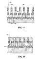
- FIG. 13is a simplified cross-sectional view of the multi-layered structure, shown in FIG. 12 after subjecting the crown surface to an etch to form via portions in the substrate in accordance with one embodiment of the present invention
- FIG. 14is a simplified cross-sectional view of the multi-layered structure, shown in FIG. 13 , after subjecting the same to an anisotropic etch to form trench portions aligned with the via portions in accordance with one embodiment of the present invention
- FIG. 15is a simplified cross-sectional view of the multi-layered structure, shown in FIG. 14 , after deposition of conductive material in the via portion and trench portion in accordance with one embodiment of the present invention
- FIG. 16is a cross-sectional view of a substrate patterned with an organic acrylate material in accordance with an alternate embodiment of the present invention.
- FIG. 17is a cross-sectional view of the substrate shown in FIG. 16 with nadir regions removed;
- FIG. 18is a cross-sectional view of the substrate shown in FIG. 17 with a conductive layer disposed thereon;
- FIG. 19is a cross-sectional view of the substrate shown in FIG. 18 after chemical mechanical polishing/planarization
- FIG. 20is a cross-sectional view of the substrate shown in FIG. 19 after removal of the organic acrylate material
- FIG. 21is a cross-sectional view of the substrate shown in FIG. 20 in accordance with an alternate embodiment
- FIG. 22is a cross-sectional view of the substrate shown in FIG. 17 with a dielectric layer disposed thereon;
- FIG. 23is a cross-sectional view of the substrate shown in FIG. 22 after being subjected to a blanket etch;
- FIG. 24is a cross-sectional view of the substrate shown in FIG. 23 after removal of the organic acrylate material
- FIG. 25is a simplified cross-sectional view of the multi-layer structure in accordance with an alternate embodiment
- FIG. 26is a simplified cross-sectional view of the multi-layer structure shown in FIG. 25 after subjecting the same to the process of FIGS. 4-9 , with the etching chemistry having a low etch selectivity;
- Multi-layer film stack 16includes a primer layer 18 deposited on a surface 20 of substrate 10 , a patterned layer 22 disposed upon primer layer 18 , and an etch-differential layer 24 deposited upon patterned layer 22 .
- Primer layer 18functions to provide surface 26 with planarity perturbations having a frequency that is less than the frequency of the planarity perturbations in surface 20 .
- each of projections 30has an apex surface 34 and each of recessions 32 has a nadir surface 36 .
- the thickness differential between t 1 and t 2 of projections 30 and recessions 32defines the amount of etch time required before exposing regions of substrate 10 .
- some or all of patterned layer 22is sacrificed during the etching process to provide the desired dimensions of the pattern eventually recorded in substrate 10 . Assuming a uniform thickness t 2 , a greater amount of etch time is required to expose regions of substrate 10 in superimposition with projections 30 compared with the time required for regions of substrate 10 in superimposition with recessions 32 .
- etchingwill commence sooner in regions of substrate 10 in superimposition with recessions 32 than regions in superimposition with projections 30 . This facilitates formation of a pattern in substrate 10 corresponding to the shape of patterned layer 22 .
- the relational dimensions between the differing features of the patternreferred to as etched pattern characteristics (EPC), eventually transferred onto substrate 10 , i.e., the recorded pattern, may be controlled as desired.
- EPCetched pattern characteristics
- planarity perturbationsmay result in exposure of some regions of substrate 10 in superimposition with projections 34 before exposure of regions of substrate 10 in superimposition with recessions 32 . As a result features of the pattern may be lost, which is undesirable.
- Etch-differential layer 24provides added variability in a given pattern transfer process for a given patterned layer by modifying the EPC. This facilitates overcoming problems associated with the planarity perturbations. Specifically, for a given etch process and patterned layer 22 , etch-differential layer 24 operates to modify the EPC by varying the time required before the etch chemistry breakthrough of all, or any sub-portion of, the patterned layer 22 to expose the region of substrate 10 in superimposition therewith.
- the modification of the EPCis dependent upon several factors.
- One of these factorsincludes the relative etch rates of the materials from which patterned layer 22 and etch-differential layer 24 are formed.
- Another factoris the variation in the spacing between normalization surface 40 and an interface of patterned layer 22 with etch-differential layer 24 , with the interface being referred to as etch rate interface (ERI) over the area of the ERI.
- ERIetch rate interface
- the variations in distance between normalization surface 40 and the ERIare a function of the shape of the relative shapes of both normalization surface 40 and patterned layer 22 . It is the volume of etch-differential layer 24 disposed between normalization surface 40 and the ERI that defines an etch-differential interface.
- etch differential interface 28provides the modification to the EPC.
- the planarity perturbationsinclude undulations 12 and polygonal structures 14 ; however, it should be understood that the topology of surface 20 may include any known shape, including substantially smooth, if not planar regions over a substantial area thereof. Further, the entire surface 20 may comprise undulations 12 , or the entire surface 20 may comprise polygonal structures 14 . Further, surface 20 may comprise of silicon and any native oxide present thereon that is associated with a standard silicon wafer or may include an indium phosphate wafer, a gallium arsenide wafer, a gallium nitride wafer and the like. Furthermore, substrate 10 may include any one of the aforementioned wafers with one or more pre-existing layer deposited thereon, any one of which may be comprised of a metallic material, a dielectric material or combination thereof.
- Primer layer 18is applied to substrate 10 employing any known technique, e.g., chemical vapor deposition techniques, atomic layer deposition techniques, physical vapor deposition techniques, spin-coating techniques, imprint lithography techniques and the like.
- primer layer 18may be formed from a material available from Brewer Science, Inc. of Rolla Mo. under the trade name DUV30J-6 that is spun-on substrate 10 .
- Primer layer 18is typically provided with a thickness to function as an anti-reflective coating and provide a continuous, smooth, relatively defect-free surface that may exhibit excellent adhesion to material deposited thereon and without being opaque to optical sensing equipment employed to detect patterns, such as alignment marks (not shown), on substrate 10 .
- Both patterned layer 22 and etch-differential layer 24are deposited using any known technique, e.g., chemical vapor deposition techniques, atomic layer deposition techniques, physical vapor deposition techniques, spin-coating techniques, imprint lithography techniques and the like.
- patterned layer 22 and etch-differential layer 24are formed employing imprint lithography techniques.
- An exemplary technique for forming patterned layer 22employs depositing a plurality of droplets of imprinting material, referred to as a drop-dispense technique.
- An exemplary drop dispense techniqueis described in U.S.
- Patterned layer 22includes the features discussed above.
- Etch-differential layer 24includes first and second opposed sides. The first side faces patterned layer 22 and has a profile complementary to the profile of the patterned layer 22 . The second side faces away from patterned layer 22 forming a substantially smooth if not planar surface, defining a normalization surface 40 .
- patterned layer 22is a polymerized and cross-linked silicon-free material formed from the following composition:
- the acrylate component isobornyl acrylatehas the following structure: and comprises approximately 55% of COMPOSITION 1 by weight, but may comprise 20-80% of the same.
- the mechanical properties of patterned layer 22are primarily attributable to IBOA.
- An exemplary sample of IBOAis available from Sigma-Aldrich of St. Louis, Mo. under product number 392103.
- the component n-hexyl acrylate (nHA)has the following structure: and comprises approximately 27% of COMPOSITION 1 by weight, but may comprise 0 to 50% of the same.
- nHAis employed to provide the desired viscosity of COMPOSITION 1, in the liquid phase, to be in a range 2-9 Centipoises. Another advantage of nHA is that it improves the flexibility of COMPOSITION 1.
- An exemplary sample of nHAis available from Sigma-Aldrich of St. Louis, Mo. under product number 408905.
- a cross-linking component, ethylene glycol diacrylatehas the following structure: and comprises approximately 15% of COMPOSITION 1 by weight, but may comprise 10-50% of the same.
- EGDAfacilitates cross-linking of nHA and IBOA during polymerization of COMPOSITION 1, as well as contributes to the modulus and stiffness build up.
- An initiator component2-hydroxy-2-methyl-1-phenyl-propan-1-one is available from Ciba Specialty Chemicals of Tarrytown, N.Y. under the trade name DAROCUR 1173, has the following structure: and comprises approximately 3% of COMPOSITION 1 by weight, but may comprise 0.1% to 5% of the same.
- the initiatoris responsive to a broad band of ultra-violet radiation to facilitate cross-linking and polymerization of the components of COMPOSITION 1.
- the component R 1 R 2is a surfactant having the general structure R 1 ⁇ F(CF 2 CF 2 ) y , with y being in a range of 1 to 7, inclusive, and R 2 ⁇ CH 2 CH 2 O(CH 2 CH 2 O) x H, with X is in a range of 0 to 15, inclusive.
- the surfactantmay be any known in the art that provides COMPOSITION 1 with suitable wetting properties in the liquid phase, as well as desired release characteristics in the solid phase.
- a surfactantis defined as any molecule, one tail of which is hydrophobic.
- Surfactantsmay be either fluorine-containing, e.g., include a fluorine chain, or may not include any fluorine in the surfactant molecule structure.
- An exemplary surfactanthas the following general structure: and is available under the trade name ZONYL® FSO-100 from DUPONTTM, which consists of 0.25 to 2% of the composition, with the remaining components being reduced a proportionate amount.
- etch differential layer 24is formed employing the drop-dispense technique discussed above with respect to patterned layer 22 .
- a plurality of droplets (not shown) of imprinting materialare deposited atop of patterned layer 22 and a planarization mold (not shown) is placed in contact therewith.
- COMPOSITION 2differs from COMPOSITION 1 by the substitution of nHA with acryloxymethylpentamethyldisiloxane that has the following structure:
- the remaining components of COMPOSITION 2are that same as COMPOSITION 1, but are present in differing amounts.
- IBOA of COMPOSITION 2typically comprises approximately 37% of COMPOSITION 2, and EGDA and 2-hydroxy-2-methyl-1-phenyl-propan-1-one, comprising approximately 18% and 3%, respectively.
- the surfactant R 1 R 2is approximately 0.5% of the COMPOSITION.
- Composition 3differs from COMPOSITION 2 only by the substitution of acryloxymethylpentamethyldisiloxane with acryloxymethylbis(trimethylsiloxy)methylsilane.
- the component acryloxymethylbis(trimethylsiloxy)methylsilanehas the following structure: The relative quantities of each of the components of COMPOSITION 3 are the same as discussed with COMPOSITION 2.
- etch-differential layer 24after formation of etch-differential layer 24 a blanket etch using, for example a RIE process with a halogen gas mixture of approximately 70% CF 4 and 30% O 2 , is employed to remove portions of etch-differential layer 24 substantially uniformly over a volume thereof to provide a crown surface 44 .
- Other gas mixturesthat may be include contains CHF 3 , SF 6 and other fluorinated chemistries know to one of ordinary skill in the etching art.
- An exemplary etch chemistryis discussed by Johnson et al. in ADVANCES IN STEP AND FLASH IMPRINT LITHOGRAPHY, in a white paper distributed at the SPIE Microlithography Conference held in Santa Clara, Calif. from Feb.
- Crown surface 44is defined by exposing the apex surface 34 of the projections 30 .
- adjacent apex surfaces 34are separated by regions 46 of etch-differential layer 24 remaining after formation of crown surface 44 .
- crown surfaceis subjected to an anisotropic etch.
- the etch chemistry of the anisotropic etchis selected to take advantage of the etch-differential provided by crown surface 44 by maximizing etching of projections 30 and segments of patterned layer 22 in superimposition therewith, while minimizing etching of regions 46 in superimposition with recessions 32 .
- advantagewas taken of the distinction of the silicon content between the patterned layer 22 and etch-differential layer 24 .
- an RIE etch with an oxygen-based chemistryit was determined that an in-situ hardened mask 48 would be created in the regions 46 proximate to the surface thereof.
- etch processessuch as a types discussed above may be employed to transfer a pattern onto substrate 10 corresponding to the recorded pattern.
- the recorded patternmay be covered with a conductive material (not shown), such as aluminum, copper, tungsten, titanium, ti-tungsten or a combination thereof and the like, to, inter alia, fill recesses in furtherance of contact formation, discussed more fully below.
- An advantage with the present inventionis that control over the dimensions of the features is facilitated despite the presence of planarity perturbations on substrate 10 .
- normalization surface 40is provided with a profile to ensure that the maximum difference between any two of distances k 2 , k 4 , k 6 , k 8 , k 10 and k 12 is less than 1 ⁇ 2 the height of the smallest projection 30 .
- Control of variations between distances, k 1 , k 3 , k 5 , k 7 , k 9 and k 11is not as critical so along as the measure of any one of distances k 1 , k 3 , k 5 , k 7 , k 9 and k 11 is no less than the measure of the largest distance among distances k 2 , k 4 , k 6 , k 8 , k 10 and k 12 .
- the distortions occurring during formation of recorded patternis substantially independent of the planarity perturbations, by decoupling the resolution of the patterning process from the resulting variations in the thickness t 2 over the area of patterned layer 22 .
- the resolution of the patterning processmay be substantially decoupled from the thickness t 2 , in addition to the variations in the same.
- the aspect ratio of the recorded patternwas defined, in part, by the difference between t 2 and t 1 .
- t 2being on the order of the size of t 1 , or larger than t 1 , would result in no features being be produced in the recorded pattern.
- the presence of planarity perturbationscontrol over thickness t 2 becomes problematic, because the same varies over the area of patterned layer 22 . This may also result in a loss of pattern features.
- the time required to imprint increased as the feature dimensions on the templatedecreased, particularly with low viscosity imprinting materials, e.g., having a viscosity of less than 25 Centipoises, wherein the patterning process is dominated by the capillary forces of the imprinting material with the template (not shown).
- compressive forcesmay be applied to reduce the time required to fill the features of the template (not shown)
- the mechanical strength of substrate 10becomes a limitation when patterning materials having high viscosity, e.g., in a range of 25 to 10,000 Centipoises.
- the compressive force required to pattern an imprinting materialis believed to increase cubically as thickness t 2 decreases.
- variations in the thickness t 2may be modified without unduly deteriorating the resolution of the features to be formed in recorded pattern.
- the difference between t 2max and t 2minmay be the same size or greater than t 1 .
- thickness t 2may be the same size as the thickness t 1 , or may be two to ten times greater than t 1 .
- An advantage with substantially increasing the thickness t 2is that the compressive forces required to achieve an imprint process may be substantially independent of thickness t 2 , which facilitates patterning process dominated by viscous forces. Further, increasing thickness t 2 facilitates reversing the tone of the pattern formed in substrate so that the tone may be commensurate with the tone of the pattern of patterned layer 22 .
- a substrate 110including a primer layer 118 , a patterned layer 122 and an etch-differential layer 124 disposed thereon, which correspond to primer layer 18 , patterned layer 22 and etch-differential layer 24 , respectively.
- Patterned layer 122includes a plurality of projections 130 and recessions 132 that are analogous to projections 30 and recession 32 .
- Projections 130extend from a nadir surface 133 , a distance h 1 , terminating in an apex surface 134 .
- a normalization surface 140defined by etch differential layer 124 , is spaced-apart from projections 130 in a manner discussed above with respect to normalization surface 40 and projections 30 .
- etch differential layer 124is subjected to a blanket etch to form conformal surface 144 in a manner discussed above with respect to forming conformal surface 44 .
- conformal surface 144is defined by exposed apex surface 134 separated by regions 146 of etch differential layer 124 .
- an RIE process with oxygen based chemistryis employed to remove projections 130 and the portions of patterned layer 122 in superimposition therewith to expose regions 150 of patterned layer 122 , forming projections 135 , spaced apart by recessions 137 .
- Projections 135include a hard mask 148 of the material from which etch-differential layer 124 is formed. Regions 150 may be closer, further or the same distance from substrate 110 than nadir surfaces 133 , dependent upon the application. A height, h 2 , of projections 135 is defined as a function of the distance regions 150 are from substrate 110 .
- regions 150are closer to substrate 110 than nadir surface 133 and provide projections 135 with a height equal to distance h 1 . Further, projections 135 are shifted in phase along the x-direction with respect to projections 130 . Particularly, projections 135 are in superimposition with the same regions of substrate 110 with which recessions 132 are in superimposition. Moreover, the dimensions of projections 135 are defined by regions 146 .
- a second etch-differential layer 224is deposited over projection 135 , filling recessions 137 .
- Etch-differential layer 224is formed from the material as discussed with respect to etch differential layer 124 .
- Etch differential layer 224has a normalization surface 240 configured in the manner discussed with respect to normalization surface 240 .
- a crown surface 244is generated in a manner discussed above with respect to crown surface 144 . This is followed by removal of projections 135 .
- the resultis that a pattern 239 , having a plurality of projections 230 and recessions 232 , is generated on substrate 110 that has the same tone as the pattern in the patterned layer 122 , i.e., one may invert the pattern obtained by the process discussed with respect to FIGS. 1-3 .
- pattern 239is shifted in phase along the X-direction with respect to pattern 139 , with the understanding that pattern 239 may shift in phase along the Y-direction, which is into the page of FIGS. 1-3 .
- pattern 239is shifted in phase in a direction so that projections 230 are in superimposition with the same regions of substrate 110 with which projections 130 are in superimposition.
- Pattern 139is said to be shifted 180° out of phase along the X and Y-directions with respect to pattern 239 .
- the remaining portions of etch differential layer 224may be removed.
- the features of the patternmay be greater than, less than or equal to the dimensions of the features in the patterned layer 122 .
- tone reversalis found when fabricating patterned layer 22 employing imprint lithography techniques. It has been found that filling of features on a template (not shown), such as recesses may be difficult if the same are too small. With the tone reversal process, the recess may be fabricated in the template (not shown) as protrusions with the same being subsequently formed into a recorded pattern as recessions. In other words, the tone of the pattern in the template may be chosen independent of the recorded tone of the recorded pattern desired. Instead, the tone of the pattern in the template may be selected to satisfy other operational characteristics of the imprint process, e.g., throughput by decreasing feature fill-time.
- patterned layer 322is shown having a plurality of features formed on substrate 310 , which include projections 330 having a thickness t 3 , shoulders 331 having a thickness t 4 and sub-portions 332 having a thickness t 5 .
- Projection 330 and shoulders 331define a bi-level projection on surface of substrate 310 .
- Thickness t 5is referred to as a residual thickness. Thicknesses “t 3 ”, “t 4 ” and “t 5 ” may be any thickness desired, dependent upon the application.
- patterned layer 322is transferred onto substrate 310 to form a via portion (not shown) and a trench portion (not shown) therein, discussed more fully below.
- substrate 310may include several preexisting layers disposed upon a wafer 312 , shown as layers 314 , 315 separated by etch stop layers 316 , 317 and 318 .
- Etch-differential layer 324is disposed adjacent to patterned layer 322 .
- Substrate 310 , patterned layer 322 and etch-differential layer 324define a multi-layered structure 338 .
- a blanket etchis employed to remove portions of etch-differential layer 324 to provide multi-layered 338 structure with the crown surface 344 .
- Crown surface 344is defined by an exposed apex surface 334 of each projection 330 and regions 346 that remain of etch-differential layer 324 after the blanket etch.
- crown surface 344is subjected to an anisotropic etch.
- the etch chemistry of the anisotropic etchis selected to maximize etching of projections 330 and the segments of patterned layer 322 in superimposition therewith, while minimizing etching of the regions 346 .
- advantagewas taken of the distinction of the silicon content between the patterned layer 322 and regions 346 to expose regions 350 of substrate 310 , as discussed above with respect to regions 46 and patterned layer 22 with respect to FIGS. 2 and 3 .
- etch processesincluding the processes discussed above, are employed to remove regions 346 and portions of multi-layered structure 338 in superimposition with regions 346 to expose regions 354 and 356 .
- Regions 354 and 356define a trench portion 358 and a via portions 360 .
- a subsequent etch process or lift-off processis employed to remove remaining portions of layers 322 and 324 .
- via portion 360 and trench portion 358may be concurrently filled with a conductive material, such as aluminum, copper, tungsten, titanium, ti-tungsten or a combination thereof and the like, to form a contact 362 and a conductive line 364 , shown in FIG. 15 .
- the advantages of this processare manifold.
- self-aligned vias and trenchesmay be formed in substrate 310 while precisely controlling the dimensions thereof. This reduces transfer distortions that may be attributable to planarity perturbations.
- etch-differential 24 layermay be formed employing spin-on techniques as discussed in U.S. patent application Ser. No. 10/789,319 filed Feb. 27, 2004 entitled COMPOSITION FOR AN ETCHING MASK COMPRISING A SILICON-CONTAINING MATERIAL.
- spin-on techniquesdiscussed in U.S. patent application Ser. No. 10/789,319 filed Feb. 27, 2004 entitled COMPOSITION FOR AN ETCHING MASK COMPRISING A SILICON-CONTAINING MATERIAL.
- hydroxyl-functional polysiloxanecomprises approximately 4% of the composition
- hexamethoxymethylmelaminecomprises approximately 0.95%
- toluenesulfonic acidcomprises approximately 0.05%
- methyl amyl ketonecomprises approximately 95%.
- hydroxyl-functional polysiloxanecomprises approximately 4% of the composition
- hexamethoxymethylmelaminecomprises approximately 0.7%
- gamma-glycidoxypropyltrimethoxysilanecomprises approximately 0.25%
- toluenesulfonic acidcomprises approximately 0.05%
- methyl amyl ketonecomprises approximately 95%.
- Both COMPOSITIONS 4 and 5are made up of at least 4% of the silicone resin.
- the quantity of silicon present in etch-differential layers 24 , 124 , 224 and 324is at least 10% by weight and typically in a range of 20% or greater.
- the quantity and composition of the solvent present in COMPOSITIONS 4 and 5is selected so that a substantial portion of the solvent evaporates during spin-coating application of the COMPOSITIONS 4 or 5 on patterned layers 22 , 122 and 322 .
- approximately 90% of the solventevaporates during spin-coating.
- the remaining 10% of the solventevaporates, leaving etch-differential layer 24 , 124 , 224 and 324 with approximately 20% silicon by weight.
- An exemplary method of forming etch-differential layers 24 , 124 , 224 and 324includes spinning-on approximately 4 mL of the silicon-containing material deposited proximate to a center of the previously deposited layer. To that end, substrates 10 , 110 or 310 are spun at 1000 rev/min for 1 minute by placing substrate 10 , 110 or 310 on a hot plate. Thereafter, the silicon-containing material is subjected to thermal energy by baking at 150° C. for 1 min. This produces the silicon-containing material from which etch-differential layer 24 , 124 , 224 and 324 is formed, with thickness variations of 20 nm or less.
- the aforementioned spin-coating and curing processesare simply repeated.
- the solvent employedis selected so as not to remove, “wash away,” silicon-containing material in a well-cured etch-differential layer.
- forming patterned layers 22 , 122 and 322 from a modified composition consisting of a mixture of COMPOSITIONs 1 and 2, when used in conjunction etch differential layers 24 , 124 , 224 and 324 , respectively, formed from one of COMPOSITIONs 4 and 5provided superior control over the anisotropy of the recessions in the recorded pattern.
- the modified compositionprovides layers 22 , 122 and 322 with approximately 2-6% of silicon by weight.
- an exemplary modified compositionconsists of 20-70% of COMPOSITION 2, with the remainder consisting of COMPOSITION 1.
- patterned layers 22 , 133 and 322with low concentrations of silicon bowing of recessions e.g., recessions 32 , 132 and 137 and 232 , was reduced, if not avoided.
- Further control over formation of the aforementioned recessionswas achieved by cooling substrates 10 , 110 and 310 to approximately zero degrees Celsius, as well as by employing reducing chemistries in lieu of the aforementioned oxidizing chemistries during etching.
- Exemplary reducing chemistriesinclude H 2 /N 2 , CO/N 2 , CH 4 /N 2 and the like.
- the aforementioned processesmay be altered to take advantage of the material of the layer upon which pattern occurs.
- patterned layers 22 , 122 and 322from COMPOSITIONS 2, 4 or 5, with etch-differential layers 24 , 124 , 224 and 324 being formed from COMPOSITION 1.
- primer layer 18from one of COMPOSITIONS 2-5, i.e., were the surface upon which primer layer 18 disposed formed from a non-silicon containing organic material.
- primer layer 18from COMPOSITION 1.
- the etch process employedwould be established to provide the desired etch selectivity in the manner similar to that described above.
- patterned layer 422is deposited on substrate 410 employing any known deposition method.
- patterned layer 422is formed from COMPOSITION 1 employing imprint lithography generated by a plurality of spaced-apart projections 430 and recessions 432 .
- a nadir portion 436 of recessions 432has a residual thickness t 6 .
- patterned layer 422is subjected to an etch process, such as an RIE oxygen etch discussed above, to remove nadir portions 436 .
- an etch processsuch as an RIE oxygen etch discussed above.
- pattern 433is formed on substrate 410 .
- a deleterious effect that occurs during removing of nadir portions 436is that an apex surface 434 of each of projections 430 assumes a faceted shape.
- a conductive materialis deposited to cover pattern 433 , including apex surfaces 434 forming a conductive layer 424 having a conforming side, conforming to a shape of pattern 433 and normalization side 440 disposed opposite to conforming side. Normalization side 440 is spaced-apart from projections 430 .
- An exemplary conductive materialis copper, but may include any of the conductive materials mentioned above.
- a suitable processmay include a chemical mechanical polishing/planarization (CMP) process forming, were conductive layer 424 formed from metal, or blanket etch were a conductive layer 424 formed from a conductive polymer.
- CMPchemical mechanical polishing/planarization
- a CMP processis employed to achieve formation of a substantially smooth, if not planar, crown surface 444 .
- the CMP processis selected based upon the material from which patterned layer 422 and conductive layer 424 are formed so that apex surfaces 434 are exposed in normalization surface having a substantially planar profile. Specifically, the faceted shape of apex surfaces is removed while providing crown surface 444 with a substantially smooth if not planar profile.
- multi-layer structure 438is subjected to an RIE process and oxygen-based chemistry, as discussed above.
- the etch processremoves projection 430 , leaving a plurality of spaced-apart metal lines 450 .
- metal lines 550may be employed to form metal lines 550 with stepped shapes, e.g., a pair of spaced-apart shoulders 552 disposed between an apex surface 530 and substrate 510 , shown in FIG. 21 .
- projections 430may be covered with a non-conductive material, e.g., a dielectric material, to form dielectric layer 624 .
- a non-conductive materiale.g., a dielectric material
- Exemplary dielectric materials included of dielectric materials applicable for this purposeare silsesquioxanes and methyl-silsesquioxanes, spin-on glass that are applied employing conventional deposition techniques.
- Dielectric layer 624covers pattern 433 , including apex surfaces 434 .
- dielectric layerincludes a conforming side, conforming to a shape of pattern 433 and normalization side 640 disposed opposite to conforming side. Normalization side 640 is spaced-apart from projections 630 .
- normalization side 640is subjected to a blanket etch, such as a CF 4 /O 2 plasma or CHF 3 /O 2 plasma etch, to expose apex surfaces 434 of projections 430 , forming a multi-layer structure 638 having a crown surface 644 .
- Crown surface 644is formed to be substantially smooth, if not, planar.
- multi-layer structure 638is subjected to an etch process that includes RIE with an oxygen plasma chemistry as discussed above.
- the etch processremoves projections 430 , leaving a plurality of spaced-apart dielectric pillars 650 . It should be understood that the same process may be employed to form dielectric pillars with stepped shapes, as discussed above.
- a multi-layered structure 700is shown having a substrate 702 , a primer layer 704 , a patterned layer 706 and an etch-differential layer 708 .
- Patterned layer 706includes projections 710 , with projections 710 being arcuate in shape.
- Multi-layered structure 700may be subjected to the process mentioned above with respect to FIGS. 4-9 , thus resulting in the formation of multi-layered structures 712 and 714 , shown in FIGS. 26 and 27 , respectively.
- the etching chemistryis such that a low etch selectivity is achieved between the patterned layer 706 and the etch-differential layer 708 .
- the etching chemistryis such that a high etch selectivity is achieved between the patterned layer 706 and the etch-differential layer 708 .
- Further processescan be undertaken that would result in different patterns being etched into substrate 702 that might be useful for generating optical elements.
- the EPCmay be modified so that the recorded pattern substantially differs from the pattern in of the patterned layer 706 .
- the etch characteristics of primer layer 704are similar to the etch characteristic of patterned layer 706 .
- primer layer 704is optional and may be omitted, dependent upon the application.
Landscapes
- Engineering & Computer Science (AREA)
- Chemical & Material Sciences (AREA)
- Nanotechnology (AREA)
- Physics & Mathematics (AREA)
- Crystallography & Structural Chemistry (AREA)
- General Physics & Mathematics (AREA)
- Mathematical Physics (AREA)
- Theoretical Computer Science (AREA)
- Condensed Matter Physics & Semiconductors (AREA)
- Manufacturing & Machinery (AREA)
- Internal Circuitry In Semiconductor Integrated Circuit Devices (AREA)
- Exposure Of Semiconductors, Excluding Electron Or Ion Beam Exposure (AREA)
Abstract
Description
- The field of invention relates generally to micro and/or nano-fabrication of structures. More particularly, the present invention is directed to forming relief structures in substrates.
- Micro-fabrication involves the fabrication of very small structures, e.g., having features on the order of micro-meters or smaller. One area in which micro-fabrication has a sizeable impact is in the semiconductor processing industry for the manufacture of integrated circuits. As the semiconductor processing industry continues to strive for larger production yields while increasing the circuits per unit area formed on a substrate, micro-fabrication becomes increasingly important. Other areas of development in which micro-fabrication has been employed include biotechnology, optical technology, mechanical systems and the like.
- Traditional micro-fabrication employs photolithography techniques to replicate patterns on substrates. Photolithography includes a combination of an exposure tool and an image transfer process. To that end, a process compatible masking layer, often referred to as a resist-layer, is employed to provide the desired pattern. That is, the material from which the resist-layer is fabricated is optimized for the exposure tool and the image transfer process. As a result, several factors are considered when determining the proper resist material, including the exposure wavelength and compatibility of the resist-layer material to post imaging processes, e.g., subsequent etch and deposition processes. In addition to the resist-layer, replicating patterns with well-defined features is dependent upon operational characteristics of the exposure tool. These characteristics include, and are not limited to, the numerical aperture of the exposure tool lens, wavelength employed and alignment systems.
- Recently a new non-photolithographic patterning process has evolved, which is commonly referred to as imprint lithography, overcoming many of the complexities and limitations of exposure tool technology. Exemplary imprint lithographic processes are described in detail in numerous publications, such as U.S. published patent application 2004/0065976, filed as U.S. patent application Ser. No. 10/264,960 on Oct. 4, 2002 and entitled METHOD AND A MOLD TO ARRANGE FEATURES ON A SUBSTRATE TO REPLICATE FEATURES HAVING MINIMAL DIMENSIONAL VARIABILITY; U.S. published patent application 2004/0065252, filed as U.S. patent application Ser. No. 10/264,926 on Oct. 4, 2002 and entitled METHOD OF FORMING A LAYER ON A SUBSTRATE TO FACILITATE FABRICATION OF METROLOGY STANDARDS; and U.S. published patent application 2004/0046271, filed as U.S. patent application Ser. No. 10/235,314 on Sep. 5, 2002 and entitled FUNCTIONAL PATTERNING MATERIAL FOR IMPRINT LITHOGRAPHY PROCESSES, all of which are assigned to the assignee of the present invention.
- The fundamental imprint lithography technique disclosed in each of the aforementioned published patent applications includes formation of a relief pattern in a polymerizable layer and transferring a pattern corresponding to the relief pattern into an underlying substrate. To that end, a template is employed spaced-apart from the substrate with a formable liquid present between the template and the substrate. The liquid is solidified to form a solidified layer that has a pattern recorded therein that is conforming to a shape of the surface of the template in contact with the liquid. The substrate and the solidified layer are then subjected to processes to transfer, into the substrate, a relief image that corresponds to the pattern in the solidified layer.
- Generally, control over the dimensions of the features formed with the aforementioned processes has been dependent upon the topology of the underlying surface in contact with the formable liquid. The greater anisotropy of the surface the greater the distortion in the relief image.
- There is a need, therefore, to provide improved processes for forming relief structures on substrates containing topography.
- The present invention features a method of patterning a substrate that includes forming, on the substrate, a first layer having a first pattern and selectively shifting in tone, as well as along a first direction, a subsequent pattern formed into the same layer that corresponds to the first pattern. To that end, one method of the present invention includes generating into the first layer, a second pattern having a shape inverse to the first pattern. A third pattern is then transferred into the first layer that has a shape inverse to the second pattern. These and other embodiments are described herein.
FIG. 1 is a simplified cross-sectional view of a multi-layered structure in accordance with one embodiment of the present invention;FIG. 2 is a simplified cross-sectional view after a blanket etch of the multi-layered structure, shown in FIG.1, to form a crown surface in accordance with one embodiment of the present invention;FIG. 3 is a simplified cross-sectional view of the multi-layered structure, shown inFIG. 2 , after subjecting the crown surface to an etch to form recesses in portions of the substrate in accordance with one embodiment of the present invention;FIG. 4 is a simplified cross-sectional view of the multi-layer structure in accordance with an alternate embodiment;FIG. 5 is a simplified cross-sectional view of the multi-layer structure shown inFIG. 4 after being subjected to a blanket etch;FIG. 6 is a simplified cross-sectional view of the multi-layered structure, shown inFIG. 5 , after subjecting a crown surface to an etch to form recesses in a primer layer;FIG. 7 is a simplified cross-sectional view of the multi-layer structure shown inFIG. 6 after deposition of a second etch differential layer;FIG. 8 is a simplified cross-sectional view of the multi-layer structure shown inFIG. 7 after being subjected to an additional blanket etch;FIG. 9 is a simplified cross-sectional view of the multi-layer structure shown inFIG. 8 after formation of recesses employing an anisotropic etch;FIG. 10 is a simplified cross-sectional view of a patterned layer disposed upon a substrate in accordance with one embodiment of the present invention;FIG. 11 is a simplified cross-sectional view of a multi-layered structure, formed by deposition of an etch-differential layer upon the patterned layer, shown inFIG. 10 ;FIG. 12 is a simplified cross-sectional view of the multi-layered structure, shown inFIG. 11 , after subjecting the same to a blanket etch to form a crown surface;FIG. 13 is a simplified cross-sectional view of the multi-layered structure, shown inFIG. 12 after subjecting the crown surface to an etch to form via portions in the substrate in accordance with one embodiment of the present invention;FIG. 14 is a simplified cross-sectional view of the multi-layered structure, shown inFIG. 13 , after subjecting the same to an anisotropic etch to form trench portions aligned with the via portions in accordance with one embodiment of the present invention;FIG. 15 is a simplified cross-sectional view of the multi-layered structure, shown inFIG. 14 , after deposition of conductive material in the via portion and trench portion in accordance with one embodiment of the present invention;FIG. 16 is a cross-sectional view of a substrate patterned with an organic acrylate material in accordance with an alternate embodiment of the present invention;FIG. 17 is a cross-sectional view of the substrate shown inFIG. 16 with nadir regions removed;FIG. 18 is a cross-sectional view of the substrate shown inFIG. 17 with a conductive layer disposed thereon;FIG. 19 is a cross-sectional view of the substrate shown inFIG. 18 after chemical mechanical polishing/planarization;FIG. 20 is a cross-sectional view of the substrate shown inFIG. 19 after removal of the organic acrylate material;FIG. 21 is a cross-sectional view of the substrate shown inFIG. 20 in accordance with an alternate embodiment;FIG. 22 is a cross-sectional view of the substrate shown inFIG. 17 with a dielectric layer disposed thereon;FIG. 23 is a cross-sectional view of the substrate shown inFIG. 22 after being subjected to a blanket etch;FIG. 24 is a cross-sectional view of the substrate shown inFIG. 23 after removal of the organic acrylate material;FIG. 25 is a simplified cross-sectional view of the multi-layer structure in accordance with an alternate embodiment;FIG. 26 is a simplified cross-sectional view of the multi-layer structure shown inFIG. 25 after subjecting the same to the process ofFIGS. 4-9 , with the etching chemistry having a low etch selectivity; andFIG. 27 is a simplified cross-sectional view of the multi-layer structure shown inFIG. 25 after subjecting the same to the process ofFIGS. 4-9 , with the etching chemistry having a high etch selectivity.- Referring to
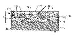
FIG. 1 , asubstrate 10, patterned in accordance with the present invention, is shown havingsurface undulations 12 and surfacepolygonal structures 14. It is problematic topattern substrate 10 with features having dimensions on the order of the dimensions ofundulations 12 andpolygonal structures 14, because thesubstrate 10 presents a non-planar, i.e., roughened topology, to the pattern process. As a result,undulations 12 andpolygonal structures 14, commonly referred to as planarity perturbations, make difficult controlling feature dimensions of patterns formed onsubstrate 10. One of the advantages of the present invention is reducing, if not abrogating, problematic effects of planarity perturbations employing amulti-layer film stack 16 to pattern the substrate underlying the surface. Multi-layer film stack 16 includes aprimer layer 18 deposited on asurface 20 ofsubstrate 10, a patternedlayer 22 disposed uponprimer layer 18, and an etch-differential layer 24 deposited upon patternedlayer 22.Primer layer 18 functions to provide surface26 with planarity perturbations having a frequency that is less than the frequency of the planarity perturbations insurface 20.Patterned layer 22 and etch-differential layer 24 define an etch ratedifferential interface 28 that results from the relative etch rates and thicknesses of the materials from which patternedlayer 22 and etch-differential layer 24 are formed. This facilitates formation, onsubstrate 10, of a pattern corresponding to a shape of patternedlayer 22. For example, as shown, patternedlayer 22 is provided with features that includeprojections 30 having a thickness t1, andrecessions 32 having a thickness t2, measured betweenprimer layer 18 and a bottom ofrecessions 32. Thickness t2is shown varying over the area of patternedlayer 22 to the planarity perturbations that presents as curved surface inprimer layer 18. Thickness t2is referred to as a residual thickness. Thicknesses “t1” and “t2” may be any thickness desired, dependent upon the application.- Each of
projections 30 has anapex surface 34 and each ofrecessions 32 has anadir surface 36. In the absence of etch-differential layer 24, the thickness differential between t1and t2ofprojections 30 andrecessions 32, respectively, defines the amount of etch time required before exposing regions ofsubstrate 10. Specifically, some or all of patternedlayer 22 is sacrificed during the etching process to provide the desired dimensions of the pattern eventually recorded insubstrate 10. Assuming a uniform thickness t2, a greater amount of etch time is required to expose regions ofsubstrate 10 in superimposition withprojections 30 compared with the time required for regions ofsubstrate 10 in superimposition withrecessions 32. For a given etching process, therefore, etching will commence sooner in regions ofsubstrate 10 in superimposition withrecessions 32 than regions in superimposition withprojections 30. This facilitates formation of a pattern insubstrate 10 corresponding to the shape of patternedlayer 22. - By properly selecting the imprinting materials and etch chemistries, the relational dimensions between the differing features of the pattern, referred to as etched pattern characteristics (EPC), eventually transferred onto
substrate 10, i.e., the recorded pattern, may be controlled as desired. To that end, it is desired that the etch characteristics of patternedlayer 22, for a given etch chemistry, be substantially uniform. However, the presence of planarity perturbations may result in exposure of some regions ofsubstrate 10 in superimposition withprojections 34 before exposure of regions ofsubstrate 10 in superimposition withrecessions 32. As a result features of the pattern may be lost, which is undesirable. - Etch-
differential layer 24 provides added variability in a given pattern transfer process for a given patterned layer by modifying the EPC. This facilitates overcoming problems associated with the planarity perturbations. Specifically, for a given etch process and patternedlayer 22, etch-differential layer 24 operates to modify the EPC by varying the time required before the etch chemistry breakthrough of all, or any sub-portion of, the patternedlayer 22 to expose the region ofsubstrate 10 in superimposition therewith. - The modification of the EPC is dependent upon several factors. One of these factors includes the relative etch rates of the materials from which patterned
layer 22 and etch-differential layer 24 are formed. Another factor is the variation in the spacing betweennormalization surface 40 and an interface of patternedlayer 22 with etch-differential layer 24, with the interface being referred to as etch rate interface (ERI) over the area of the ERI. The variations in distance betweennormalization surface 40 and the ERI are a function of the shape of the relative shapes of bothnormalization surface 40 and patternedlayer 22. It is the volume of etch-differential layer 24 disposed betweennormalization surface 40 and the ERI that defines an etch-differential interface. Considering that all or some of etch-differential layer 24 and some or all of patternedlayer 22 are sacrificed to form ontosubstrate 10 the desired recoded pattern, it is seen that etchdifferential interface 28 provides the modification to the EPC. By establishing a suitable etch-differential interface 28, the deleterious effects of planarity perturbations may be attenuated, if not avoided. - For example, as mentioned above, the planarity perturbations include
undulations 12 andpolygonal structures 14; however, it should be understood that the topology ofsurface 20 may include any known shape, including substantially smooth, if not planar regions over a substantial area thereof. Further, theentire surface 20 may compriseundulations 12, or theentire surface 20 may comprisepolygonal structures 14. Further,surface 20 may comprise of silicon and any native oxide present thereon that is associated with a standard silicon wafer or may include an indium phosphate wafer, a gallium arsenide wafer, a gallium nitride wafer and the like. Furthermore,substrate 10 may include any one of the aforementioned wafers with one or more pre-existing layer deposited thereon, any one of which may be comprised of a metallic material, a dielectric material or combination thereof. Primer layer 18 is applied tosubstrate 10 employing any known technique, e.g., chemical vapor deposition techniques, atomic layer deposition techniques, physical vapor deposition techniques, spin-coating techniques, imprint lithography techniques and the like. In the present example,primer layer 18 may be formed from a material available from Brewer Science, Inc. of Rolla Mo. under the trade name DUV30J-6 that is spun-onsubstrate 10.Primer layer 18 is typically provided with a thickness to function as an anti-reflective coating and provide a continuous, smooth, relatively defect-free surface that may exhibit excellent adhesion to material deposited thereon and without being opaque to optical sensing equipment employed to detect patterns, such as alignment marks (not shown), onsubstrate 10.- Both patterned
layer 22 and etch-differential layer 24 are deposited using any known technique, e.g., chemical vapor deposition techniques, atomic layer deposition techniques, physical vapor deposition techniques, spin-coating techniques, imprint lithography techniques and the like. In the present example, patternedlayer 22 and etch-differential layer 24 are formed employing imprint lithography techniques. An exemplary technique for forming patternedlayer 22 employs depositing a plurality of droplets of imprinting material, referred to as a drop-dispense technique. An exemplary drop dispense technique is described in U.S. patent application Ser. No. 10/789,319 filed Feb. 27, 2004 entitled COMPOSITION FOR AN ETCHING MASK COMPRISING A SILICON-CONTAINING MATERIAL, which is assigned to the assignee of the present invention and incorporated by reference herein. Typically, drop dispense imprinting is practiced in a helium rich atmosphere, e.g., with helium being flowed into a process region at about 5 pounds per square inch, in a manner described in U.S. patent application Ser. No. 10/677,639, entitled SINGLE PHASE FLUID IMPRINT LITHOGRAPHY METHOD filed Oct. 2, 2003 and is incorporated by reference herein. An exemplary system is available under the trade name IMPRIO 100™ from Molecular Imprints, Inc. having a place of business at 1807-C Braker Lane, Suite 100, Austin, Tex. 78758. The system description for the IMPRIO 100™ is available at www.molecularimprints.com and is incorporated herein by reference. Patterned layer 22 includes the features discussed above. Etch-differential layer 24 includes first and second opposed sides. The first side faces patternedlayer 22 and has a profile complementary to the profile of the patternedlayer 22. The second side faces away from patternedlayer 22 forming a substantially smooth if not planar surface, defining anormalization surface 40.- The materials employed to form the patterned
layer 22 and etch-differential layer 24 are selected to obtain the desired etch-differential interface 28. In one example, patternedlayer 22 is a polymerized and cross-linked silicon-free material formed from the following composition: - The acrylate component isobornyl acrylate (IBOA) has the following structure:

and comprises approximately 55% of COMPOSITION 1 by weight, but may comprise 20-80% of the same. As a result, the mechanical properties of patterned layer22 are primarily attributable to IBOA. An exemplary sample of IBOA is available from Sigma-Aldrich of St. Louis, Mo. under product number 392103. The component n-hexyl acrylate (nHA) has the following structure:
and comprises approximately 27% of COMPOSITION 1 by weight, but may comprise 0 to 50% of the same. Also providing mechanical strength to patterned layer22, nHA is employed to provide the desired viscosity of COMPOSITION 1, in the liquid phase, to be in a range 2-9 Centipoises. Another advantage of nHA is that it improves the flexibility of COMPOSITION 1. An exemplary sample of nHA is available from Sigma-Aldrich of St. Louis, Mo. under product number 408905. A cross-linking component, ethylene glycol diacrylate, has the following structure:
and comprises approximately 15% of COMPOSITION 1 by weight, but may comprise 10-50% of the same. EGDA facilitates cross-linking of nHA and IBOA during polymerization of COMPOSITION 1, as well as contributes to the modulus and stiffness build up. An initiator component, 2-hydroxy-2-methyl-1-phenyl-propan-1-one is available from Ciba Specialty Chemicals of Tarrytown, N.Y. under the trade name DAROCUR 1173, has the following structure:
and comprises approximately 3% of COMPOSITION 1 by weight, but may comprise 0.1% to 5% of the same. The initiator is responsive to a broad band of ultra-violet radiation to facilitate cross-linking and polymerization of the components of COMPOSITION 1. - The component R1R2is a surfactant having the general structure R1═F(CF2CF2)y, with y being in a range of 1 to 7, inclusive, and R2═CH2CH2O(CH2CH2O)xH, with X is in a range of 0 to 15, inclusive. The surfactant may be any known in the art that provides COMPOSITION 1 with suitable wetting properties in the liquid phase, as well as desired release characteristics in the solid phase. For purposes of this invention a surfactant is defined as any molecule, one tail of which is hydrophobic. Surfactants may be either fluorine-containing, e.g., include a fluorine chain, or may not include any fluorine in the surfactant molecule structure. An exemplary surfactant has the following general structure:

and is available under the trade name ZONYL® FSO-100 from DUPONT™, which consists of 0.25 to 2% of the composition, with the remaining components being reduced a proportionate amount. - In the present example, etch
differential layer 24 is formed employing the drop-dispense technique discussed above with respect to patternedlayer 22. As a result, a plurality of droplets (not shown) of imprinting material are deposited atop of patternedlayer 22 and a planarization mold (not shown) is placed in contact therewith. Exemplary imprinting materials from which etch-differential layer 24 is a polymerized and cross-linked material formed from one of the following compositions: - COMPOSITION 2 differs from COMPOSITION 1 by the substitution of nHA with acryloxymethylpentamethyldisiloxane that has the following structure:

The remaining components of COMPOSITION 2 are that same as COMPOSITION 1, but are present in differing amounts. For example, IBOA of COMPOSITION 2 typically comprises approximately 37% of COMPOSITION 2, and EGDA and 2-hydroxy-2-methyl-1-phenyl-propan-1-one, comprising approximately 18% and 3%, respectively. The surfactant R1R2is approximately 0.5% of the COMPOSITION. - Composition 3 differs from COMPOSITION 2 only by the substitution of acryloxymethylpentamethyldisiloxane with acryloxymethylbis(trimethylsiloxy)methylsilane. The component acryloxymethylbis(trimethylsiloxy)methylsilane has the following structure:

The relative quantities of each of the components of COMPOSITION 3 are the same as discussed with COMPOSITION 2. - Referring to
FIGS. 1 and 2 , after formation of etch-differential layer24 a blanket etch using, for example a RIE process with a halogen gas mixture of approximately 70% CF4and 30% O2, is employed to remove portions of etch-differential layer 24 substantially uniformly over a volume thereof to provide acrown surface 44. Other gas mixtures that may be include contains CHF3, SF6and other fluorinated chemistries know to one of ordinary skill in the etching art. An exemplary etch chemistry is discussed by Johnson et al. in ADVANCES IN STEP AND FLASH IMPRINT LITHOGRAPHY, in a white paper distributed at the SPIE Microlithography Conference held in Santa Clara, Calif. from Feb. 23-Feb. 28, 2003.Crown surface 44 is defined by exposing theapex surface 34 of theprojections 30. In the present example, adjacent apex surfaces34 are separated byregions 46 of etch-differential layer 24 remaining after formation ofcrown surface 44. - Referring to
FIGS. 2 and 3 , crown surface is subjected to an anisotropic etch. The etch chemistry of the anisotropic etch is selected to take advantage of the etch-differential provided bycrown surface 44 by maximizing etching ofprojections 30 and segments of patternedlayer 22 in superimposition therewith, while minimizing etching ofregions 46 in superimposition withrecessions 32. In the present example, advantage was taken of the distinction of the silicon content between the patternedlayer 22 and etch-differential layer 24. Specifically, employing an RIE etch with an oxygen-based chemistry, it was determined that an in-situ hardenedmask 48 would be created in theregions 46 proximate to the surface thereof. This results from the interaction of the silicon-containing polymerizable material with the oxygen plasma. As a result of hardenedmask 48 and the anisotropy of the etch process, portions of patterned layers are removed substantially uniformly over the volume thereof to exposeregions 50 ofsubstrate 10 in superimposition withprojections 30. In this manner, a recorded pattern is formed that is defined bypillars 52 and recesses54. - After exposure of
regions 50, suitable etch processes, such as a types discussed above may be employed to transfer a pattern ontosubstrate 10 corresponding to the recorded pattern. Alternatively, or in conjunction therewith, the recorded pattern may be covered with a conductive material (not shown), such as aluminum, copper, tungsten, titanium, ti-tungsten or a combination thereof and the like, to, inter alia, fill recesses in furtherance of contact formation, discussed more fully below. - An advantage with the present invention is that control over the dimensions of the features is facilitated despite the presence of planarity perturbations on
substrate 10. This is achieved by ensuring thatnormalization surface 40 is provided with a profile to ensure that distances k2, k4, k6, k8, k10and k12betweenapex surfaces 34 of each ofprojections 30 andnormalization surface 40 are within a predetermined range. Specifically,normalization surface 40 is provided with a profile to ensure that the maximum difference between any two of distances k2, k4, k6, k8, k10and k12is less than ½ the height of thesmallest projection 30. Control of variations between distances, k1, k3, k5, k7, k9and k11is not as critical so along as the measure of any one of distances k1, k3, k5, k7, k9and k11is no less than the measure of the largest distance among distances k2, k4, k6, k8, k10and k12. With this criteria being satisfied, the distortions occurring during formation of recorded pattern is substantially independent of the planarity perturbations, by decoupling the resolution of the patterning process from the resulting variations in the thickness t2over the area of patternedlayer 22. - It was also determined that the resolution of the patterning process may be substantially decoupled from the thickness t2, in addition to the variations in the same. Specifically, without the presence of etch-
differential layer 24, the aspect ratio of the recorded pattern was defined, in part, by the difference between t2and t1. In the absence of planarity perturbations, t2being on the order of the size of t1, or larger than t1, would result in no features being be produced in the recorded pattern. As a result, it was highly desired to minimize the thickness of t2. Further, the presence of planarity perturbations, control over thickness t2becomes problematic, because the same varies over the area of patternedlayer 22. This may also result in a loss of pattern features. Specifically, assume a maximum value of t2, t2max, and a minimum value of t2, t2min. Were the difference between t2maxand t2minon the order of the size of t1, or larger than t1, features in the recorded pattern would be lost. Further, the speed at which the patterning process occurred was often decreased due to the time required to fill the features of a template (not shown). Also, the time required to imprint increased as the feature dimensions on the template decreased, particularly with low viscosity imprinting materials, e.g., having a viscosity of less than 25 Centipoises, wherein the patterning process is dominated by the capillary forces of the imprinting material with the template (not shown). Although compressive forces may be applied to reduce the time required to fill the features of the template (not shown), there are limits, e.g., the mechanical strength of theunderlying substrate 10 to mention one. The mechanical strength ofsubstrate 10 becomes a limitation when patterning materials having high viscosity, e.g., in a range of 25 to 10,000 Centipoises. At the greater range of viscosity the patterning process becomes dominated by viscous forces of the imprinting material, as opposed to capillary forces. The compressive force required to pattern an imprinting material is believed to increase cubically as thickness t2decreases. - With the present invention, variations in the thickness t2, as well as the overall thickness may be modified without unduly deteriorating the resolution of the features to be formed in recorded pattern. For example, the difference between t2maxand t2minmay be the same size or greater than t1. Additionally, thickness t2may be the same size as the thickness t1, or may be two to ten times greater than t1. An advantage with substantially increasing the thickness t2is that the compressive forces required to achieve an imprint process may be substantially independent of thickness t2, which facilitates patterning process dominated by viscous forces. Further, increasing thickness t2facilitates reversing the tone of the pattern formed in substrate so that the tone may be commensurate with the tone of the pattern of patterned
layer 22. - Referring to
FIGS. 1 and 4 asubstrate 110 is shown including aprimer layer 118, apatterned layer 122 and an etch-differential layer 124 disposed thereon, which correspond toprimer layer 18, patternedlayer 22 and etch-differential layer 24, respectively.Patterned layer 122 includes a plurality ofprojections 130 andrecessions 132 that are analogous toprojections 30 andrecession 32.Projections 130 extend from anadir surface 133, a distance h1, terminating in anapex surface 134. Anormalization surface 140, defined byetch differential layer 124, is spaced-apart fromprojections 130 in a manner discussed above with respect tonormalization surface 40 andprojections 30. - Referring to
FIGS. 1, 4 and5, etchdifferential layer 124 is subjected to a blanket etch to formconformal surface 144 in a manner discussed above with respect to formingconformal surface 44. To that end,conformal surface 144 is defined by exposedapex surface 134 separated byregions 146 of etchdifferential layer 124. - Referring to
FIGS. 5 and 6 , following formation ofcrown surface 144, an RIE process with oxygen based chemistry is employed to removeprojections 130 and the portions of patternedlayer 122 in superimposition therewith to exposeregions 150 of patternedlayer 122, formingprojections 135, spaced apart byrecessions 137.Projections 135 include ahard mask 148 of the material from which etch-differential layer 124 is formed.Regions 150 may be closer, further or the same distance fromsubstrate 110 than nadir surfaces133, dependent upon the application. A height, h2, ofprojections 135 is defined as a function of thedistance regions 150 are fromsubstrate 110. In the present example,regions 150 are closer tosubstrate 110 thannadir surface 133 and provideprojections 135 with a height equal to distance h1. Further,projections 135 are shifted in phase along the x-direction with respect toprojections 130. Particularly,projections 135 are in superimposition with the same regions ofsubstrate 110 with whichrecessions 132 are in superimposition. Moreover, the dimensions ofprojections 135 are defined byregions 146. - Referring to
FIGS. 6 and 7 , afterprojections 135 have been formed, a second etch-differential layer 224 is deposited overprojection 135, fillingrecessions 137. Etch-differential layer 224 is formed from the material as discussed with respect to etchdifferential layer 124. Etchdifferential layer 224 has anormalization surface 240 configured in the manner discussed with respect tonormalization surface 240. - Referring to
FIGS. 7, 8 , and9, acrown surface 244 is generated in a manner discussed above with respect tocrown surface 144. This is followed by removal ofprojections 135. The result is that apattern 239, having a plurality ofprojections 230 andrecessions 232, is generated onsubstrate 110 that has the same tone as the pattern in the patternedlayer 122, i.e., one may invert the pattern obtained by the process discussed with respect toFIGS. 1-3 . Additionally, as shownpattern 239 is shifted in phase along the X-direction with respect topattern 139, with the understanding thatpattern 239 may shift in phase along the Y-direction, which is into the page ofFIGS. 1-3 . Specifically,pattern 239 is shifted in phase in a direction so thatprojections 230 are in superimposition with the same regions ofsubstrate 110 with whichprojections 130 are in superimposition.Pattern 139, therefore, is said to be shifted 180° out of phase along the X and Y-directions with respect topattern 239. Subsequently, the remaining portions of etchdifferential layer 224 may be removed. By appropriately selecting the characteristics of the etch process, the features of the pattern may be greater than, less than or equal to the dimensions of the features in the patternedlayer 122. - Another advantage with the tone reversal is found when fabricating patterned
layer 22 employing imprint lithography techniques. It has been found that filling of features on a template (not shown), such as recesses may be difficult if the same are too small. With the tone reversal process, the recess may be fabricated in the template (not shown) as protrusions with the same being subsequently formed into a recorded pattern as recessions. In other words, the tone of the pattern in the template may be chosen independent of the recorded tone of the recorded pattern desired. Instead, the tone of the pattern in the template may be selected to satisfy other operational characteristics of the imprint process, e.g., throughput by decreasing feature fill-time. - It should be understood that the benefits of the aforementioned processes is not limited to forming patterns having single-recessed-level features, as discussed above, but may also be employed forming patterns having bi-level recessed features, i.e., stepped features. For example, referring to
FIGS. 10 and 11 , patternedlayer 322 is shown having a plurality of features formed onsubstrate 310, which includeprojections 330 having a thickness t3, shoulders331 having a thickness t4and sub-portions332 having a thickness t5.Projection 330 andshoulders 331 define a bi-level projection on surface ofsubstrate 310. Thickness t5is referred to as a residual thickness. Thicknesses “t3”, “t4” and “t5” may be any thickness desired, dependent upon the application. - An inverse shape of patterned
layer 322 is transferred ontosubstrate 310 to form a via portion (not shown) and a trench portion (not shown) therein, discussed more fully below. In this manner, the dimensions of the via portion (not shown) are established as a function of the dimensions of projections, and the dimensions of the trench portion (not shown) are established as a function of the dimensions of the shoulders. To that end,substrate 310 may include several preexisting layers disposed upon awafer 312, shown aslayers differential layer 324 is disposed adjacent to patternedlayer 322.Substrate 310, patternedlayer 322 and etch-differential layer 324 define amulti-layered structure 338. - Referring to
FIGS. 11 and 12 , a blanket etch is employed to remove portions of etch-differential layer 324 to provide multi-layered338 structure with thecrown surface 344.Crown surface 344 is defined by an exposedapex surface 334 of eachprojection 330 andregions 346 that remain of etch-differential layer 324 after the blanket etch. - Referring to
FIGS. 12 and 13 ,crown surface 344 is subjected to an anisotropic etch. The etch chemistry of the anisotropic etch is selected to maximize etching ofprojections 330 and the segments of patternedlayer 322 in superimposition therewith, while minimizing etching of theregions 346. In the present example, advantage was taken of the distinction of the silicon content between thepatterned layer 322 andregions 346 to exposeregions 350 ofsubstrate 310, as discussed above with respect toregions 46 and patternedlayer 22 with respect toFIGS. 2 and 3 . - Referring to
FIGS. 13 and 14 , after exposure ofregions 350, suitable etch processes, including the processes discussed above, are employed to removeregions 346 and portions ofmulti-layered structure 338 in superimposition withregions 346 to exposeregions Regions trench portion 358 and a viaportions 360. A subsequent etch process or lift-off process is employed to remove remaining portions oflayers portion 360 andtrench portion 358 may be concurrently filled with a conductive material, such as aluminum, copper, tungsten, titanium, ti-tungsten or a combination thereof and the like, to form acontact 362 and aconductive line 364, shown inFIG. 15 . - Referring to
FIGS. 2, 13 and14, the advantages of this process are manifold. For example, self-aligned vias and trenches may be formed insubstrate 310 while precisely controlling the dimensions thereof. This reduces transfer distortions that may be attributable to planarity perturbations. - Although the foregoing has been discussed with respect to forming etch-
differential layer 24 using drop-dispense techniques, etch-differential24 layer may be formed employing spin-on techniques as discussed in U.S. patent application Ser. No. 10/789,319 filed Feb. 27, 2004 entitled COMPOSITION FOR AN ETCHING MASK COMPRISING A SILICON-CONTAINING MATERIAL. To that end, the following compositions may be employed: - In COMPOSITION 4, hydroxyl-functional polysiloxane comprises approximately 4% of the composition, hexamethoxymethylmelamine comprises approximately 0.95%, toluenesulfonic acid comprises approximately 0.05% and methyl amyl ketone comprises approximately 95%. In COMPOSITION 5, hydroxyl-functional polysiloxane comprises approximately 4% of the composition, hexamethoxymethylmelamine comprises approximately 0.7%, gamma-glycidoxypropyltrimethoxysilane comprises approximately 0.25%, toluenesulfonic acid comprises approximately 0.05%, and methyl amyl ketone comprises approximately 95%.
- Both COMPOSITIONS 4 and 5 are made up of at least 4% of the silicone resin. Upon curing, however, the quantity of silicon present in etch-
differential layers layers differential layer - An exemplary method of forming etch-
differential layers substrates substrate differential layer - Referring to
FIGS. 1-14 , it has been determined, however, that formingpatterned layers differential layers layers patterned layers patterned layers recessions substrates - Additionally, should circumstances warrant, the aforementioned processes may be altered to take advantage of the material of the layer upon which pattern occurs. For example, it is possible to form patterned
layers differential layers primer layer 18 from one of COMPOSITIONS 2-5, i.e., were the surface upon whichprimer layer 18 disposed formed from a non-silicon containing organic material. Additionally, it is possible to formprimer layer 18 from COMPOSITION 1. The etch process employed would be established to provide the desired etch selectivity in the manner similar to that described above. - Referring to
FIG. 16 , other processes in which an organic patterned layer functions as a sacrificial patterning layer may include formation of metal lines. To that end, patternedlayer 422 is deposited onsubstrate 410 employing any known deposition method. In the present example, patternedlayer 422 is formed from COMPOSITION 1 employing imprint lithography generated by a plurality of spaced-apart projections 430 andrecessions 432. Anadir portion 436 ofrecessions 432 has a residual thickness t6. - Referring to
FIGS. 16 and 17 , patternedlayer 422 is subjected to an etch process, such as an RIE oxygen etch discussed above, to removenadir portions 436. As a result of this process,pattern 433 is formed onsubstrate 410. A deleterious effect that occurs during removing ofnadir portions 436 is that anapex surface 434 of each ofprojections 430 assumes a faceted shape. - Referring to
FIGS. 17 and 18 , a conductive material is deposited to coverpattern 433, includingapex surfaces 434 forming aconductive layer 424 having a conforming side, conforming to a shape ofpattern 433 andnormalization side 440 disposed opposite to conforming side.Normalization side 440 is spaced-apart fromprojections 430. An exemplary conductive material is copper, but may include any of the conductive materials mentioned above. - Referring to
FIGS. 18 and 19 , following deposition ofconductive layer 424,normalization side 440 is subjected to suitable processes to formmulti-layer structure 438. A suitable process may include a chemical mechanical polishing/planarization (CMP) process forming, wereconductive layer 424 formed from metal, or blanket etch were aconductive layer 424 formed from a conductive polymer. In the present example, a CMP process is employed to achieve formation of a substantially smooth, if not planar,crown surface 444. To that end, the CMP process is selected based upon the material from which patternedlayer 422 andconductive layer 424 are formed so thatapex surfaces 434 are exposed in normalization surface having a substantially planar profile. Specifically, the faceted shape of apex surfaces is removed while providingcrown surface 444 with a substantially smooth if not planar profile. - Referring to
FIGS. 19 and 20 , following formation ofcrown surface 444,multi-layer structure 438 is subjected to an RIE process and oxygen-based chemistry, as discussed above. The etch process removesprojection 430, leaving a plurality of spaced-apartmetal lines 450. It should understood that the this same process may be employed to form metal lines550 with stepped shapes, e.g., a pair of spaced-apart shoulders 552 disposed between anapex surface 530 andsubstrate 510, shown inFIG. 21 . - Referring to
FIGS. 17 and 22 ,projections 430 may be covered with a non-conductive material, e.g., a dielectric material, to formdielectric layer 624. Exemplary dielectric materials included of dielectric materials applicable for this purpose are silsesquioxanes and methyl-silsesquioxanes, spin-on glass that are applied employing conventional deposition techniques.Dielectric layer 624 coverspattern 433, including apex surfaces434. As a result, dielectric layer includes a conforming side, conforming to a shape ofpattern 433 andnormalization side 640 disposed opposite to conforming side.Normalization side 640 is spaced-apart from projections630. - Referring to
FIGS. 22 and 23 , following deposition ofdielectric layer 624,normalization side 640 is subjected to a blanket etch, such as a CF4/O2plasma or CHF3/O2plasma etch, to exposeapex surfaces 434 ofprojections 430, forming amulti-layer structure 638 having acrown surface 644.Crown surface 644 is formed to be substantially smooth, if not, planar. - Referring to
FIGS. 23 and 24 , following formation ofcrown surface 644,multi-layer structure 638 is subjected to an etch process that includes RIE with an oxygen plasma chemistry as discussed above. The etch process removesprojections 430, leaving a plurality of spaced-apartdielectric pillars 650. It should be understood that the same process may be employed to form dielectric pillars with stepped shapes, as discussed above. - Referring to
FIG. 25 , amulti-layered structure 700 is shown having asubstrate 702, aprimer layer 704, apatterned layer 706 and an etch-differential layer 708.Patterned layer 706 includesprojections 710, withprojections 710 being arcuate in shape.Multi-layered structure 700 may be subjected to the process mentioned above with respect toFIGS. 4-9 , thus resulting in the formation ofmulti-layered structures FIGS. 26 and 27 , respectively. In a first embodiment, the etching chemistry is such that a low etch selectivity is achieved between thepatterned layer 706 and the etch-differential layer 708. In a second embodiment, the etching chemistry is such that a high etch selectivity is achieved between thepatterned layer 706 and the etch-differential layer 708. Further processes can be undertaken that would result in different patterns being etched intosubstrate 702 that might be useful for generating optical elements. Particularly, by tailoring the relative etch rates, and relative thicknesses ofdifferential layer 708, patternedlayer 706 andprimer layer 704, the EPC may be modified so that the recorded pattern substantially differs from the pattern in of the patternedlayer 706. It should be understood that the etch characteristics ofprimer layer 704 are similar to the etch characteristic of patternedlayer 706. Furthermore,primer layer 704 is optional and may be omitted, dependent upon the application. - The embodiments of the present invention described above are exemplary. Many changes and modifications may be made to the disclosure recited above, while remaining within the scope of the invention. The scope of the invention should, therefore, be determined not with reference to the above description, but instead should be determined with reference to the appended claims along with their full scope of equivalents.


Claims (21)
Priority Applications (14)
| Application Number | Priority Date | Filing Date | Title |
|---|---|---|---|
| US10/946,566US7547504B2 (en) | 2004-09-21 | 2004-09-21 | Pattern reversal employing thick residual layers |
| SG200807517-8ASG147419A1 (en) | 2004-09-21 | 2005-09-12 | Method of forming an in-situ recessed structure |
| SG200807516-0ASG147418A1 (en) | 2004-09-21 | 2005-09-12 | Method of forming an in-situ recessed structure |
| EP09173395AEP2146369A3 (en) | 2004-09-21 | 2005-09-12 | Method of forming an in-situ recessed structure |
| SG200807515-2ASG147417A1 (en) | 2004-09-21 | 2005-09-12 | Method of forming an in-situ recessed structure |
| KR1020117030614AKR101262730B1 (en) | 2004-09-21 | 2005-09-12 | Method of forming an in-situ recessed structure |
| JP2007532387AJP2008513229A (en) | 2004-09-21 | 2005-09-12 | In-situ insertion structure forming method |
| PCT/US2005/032276WO2006033872A2 (en) | 2004-09-21 | 2005-09-12 | Method of forming an in-situ recessed structure |
| EP05796480AEP1794099A4 (en) | 2004-09-21 | 2005-09-12 | Method of forming an in-situ recessed structure |
| SG200807518-6ASG147420A1 (en) | 2004-09-21 | 2005-09-12 | Method of forming an in-situ recessed structure |
| KR1020077006500AKR101243646B1 (en) | 2004-09-21 | 2005-09-12 | Method of forming an in-situ recessed structure |
| EP09173416AEP2146370A3 (en) | 2004-09-21 | 2005-09-12 | Method of forming an in-situ recessed structure |
| TW094132119ATWI292590B (en) | 2004-09-21 | 2005-09-16 | Pattern reversal employing thick residual layers |
| JP2014042722AJP5848386B2 (en) | 2004-09-21 | 2014-03-05 | In-situ insertion structure forming method |
Applications Claiming Priority (1)
| Application Number | Priority Date | Filing Date | Title |
|---|---|---|---|
| US10/946,566US7547504B2 (en) | 2004-09-21 | 2004-09-21 | Pattern reversal employing thick residual layers |
Publications (2)
| Publication Number | Publication Date |
|---|---|
| US20060063112A1true US20060063112A1 (en) | 2006-03-23 |
| US7547504B2 US7547504B2 (en) | 2009-06-16 |
Family
ID=36074464
Family Applications (1)
| Application Number | Title | Priority Date | Filing Date |
|---|---|---|---|
| US10/946,566Active2026-12-07US7547504B2 (en) | 2004-09-21 | 2004-09-21 | Pattern reversal employing thick residual layers |
Country Status (2)
| Country | Link |
|---|---|
| US (1) | US7547504B2 (en) |
| TW (1) | TWI292590B (en) |
Cited By (26)
| Publication number | Priority date | Publication date | Assignee | Title |
|---|---|---|---|---|
| US20060063277A1 (en)* | 2004-09-21 | 2006-03-23 | Molecular Imprints, Inc. | Method of forming an in-situ recessed structure |
| US20070126150A1 (en)* | 2005-12-01 | 2007-06-07 | Molecular Imprints, Inc. | Bifurcated contact printing technique |
| US20070132152A1 (en)* | 2005-12-08 | 2007-06-14 | Molecular Imprints, Inc. | Method and System for Double-Sided Patterning of Substrates |
| US20070170617A1 (en)* | 2006-01-20 | 2007-07-26 | Molecular Imprints, Inc. | Patterning Substrates Employing Multiple Chucks |
| US20080118872A1 (en)* | 2003-03-25 | 2008-05-22 | Molecular Imprints, Inc. | Positive Tone Bi-Layer Method |
| US20080141862A1 (en)* | 2003-10-02 | 2008-06-19 | Molecular Imprints, Inc. | Single Phase Fluid Imprint Lithography Method |
| US7396475B2 (en) | 2003-04-25 | 2008-07-08 | Molecular Imprints, Inc. | Method of forming stepped structures employing imprint lithography |
| US20080174046A1 (en)* | 2002-07-11 | 2008-07-24 | Molecular Imprints Inc. | Capillary Imprinting Technique |
| US20080292976A1 (en)* | 2007-05-23 | 2008-11-27 | Canon Kabushiki Kaisha | Pattern forming method, pattern formed thereby, mold, processing apparatus, and processing method |
| US20080303187A1 (en)* | 2006-12-29 | 2008-12-11 | Molecular Imprints, Inc. | Imprint Fluid Control |
| US20080308971A1 (en)* | 2007-06-18 | 2008-12-18 | Molecular Imprints, Inc. | Solvent-Assisted Layer Formation for Imprint Lithography |
| US20090014917A1 (en)* | 2007-07-10 | 2009-01-15 | Molecular Imprints, Inc. | Drop Pattern Generation for Imprint Lithography |
| US20090115110A1 (en)* | 2007-11-02 | 2009-05-07 | Molecular Imprints, Inc. | Drop Pattern Generation for Imprint Lithography |
| US20090148619A1 (en)* | 2007-12-05 | 2009-06-11 | Molecular Imprints, Inc. | Controlling Thickness of Residual Layer |
| US20090200710A1 (en)* | 2008-02-08 | 2009-08-13 | Molecular Imprints, Inc. | Extrusion reduction in imprint lithography |
| US7691313B2 (en) | 2002-11-13 | 2010-04-06 | Molecular Imprints, Inc. | Method for expelling gas positioned between a substrate and a mold |
| US20100096764A1 (en)* | 2008-10-20 | 2010-04-22 | Molecular Imprints, Inc. | Gas Environment for Imprint Lithography |
| US20100098859A1 (en)* | 2008-10-21 | 2010-04-22 | Molecular Imprints, Inc. | Drop Pattern Generation with Edge Weighting |
| US20100112220A1 (en)* | 2008-11-03 | 2010-05-06 | Molecular Imprints, Inc. | Dispense system set-up and characterization |
| US7981481B2 (en) | 2004-09-23 | 2011-07-19 | Molecular Imprints, Inc. | Method for controlling distribution of fluid components on a body |
| US7985530B2 (en) | 2006-09-19 | 2011-07-26 | Molecular Imprints, Inc. | Etch-enhanced technique for lift-off patterning |
| US8215946B2 (en) | 2006-05-18 | 2012-07-10 | Molecular Imprints, Inc. | Imprint lithography system and method |
| US20130074765A1 (en)* | 2010-05-27 | 2013-03-28 | Inca Digital Printers Limited | Method of adjusting surface topography |
| US8586126B2 (en) | 2008-10-21 | 2013-11-19 | Molecular Imprints, Inc. | Robust optimization to generate drop patterns in imprint lithography which are tolerant of variations in drop volume and drop placement |
| EP2847233A4 (en)* | 2012-06-06 | 2016-02-17 | Canon Kk | Curable composition and patterning method using the same |
| US11029597B2 (en) | 2016-02-29 | 2021-06-08 | Fujifilm Corporation | Method for producing pattern laminate, method for producing reversal pattern, and pattern laminate |
Families Citing this family (11)
| Publication number | Priority date | Publication date | Assignee | Title |
|---|---|---|---|---|
| US7162035B1 (en) | 2000-05-24 | 2007-01-09 | Tracer Detection Technology Corp. | Authentication method and system |
| US7259102B2 (en)* | 2005-09-30 | 2007-08-21 | Molecular Imprints, Inc. | Etching technique to planarize a multi-layer structure |
| US7995196B1 (en) | 2008-04-23 | 2011-08-09 | Tracer Detection Technology Corp. | Authentication method and system |
| WO2010111307A1 (en)* | 2009-03-23 | 2010-09-30 | Intevac, Inc. | A process for optimization of island to trench ratio in patterned media |
| US10026436B2 (en)* | 2009-07-01 | 2018-07-17 | Nordson Corporation | Apparatus and methods for supporting workpieces during plasma processing |
| EP2718465B1 (en) | 2011-06-09 | 2022-04-13 | Illumina, Inc. | Method of making an analyte array |
| CA2856163C (en) | 2011-10-28 | 2019-05-07 | Illumina, Inc. | Microarray fabrication system and method |
| KR102279239B1 (en) | 2014-07-25 | 2021-07-19 | 삼성전자주식회사 | Method of transferring reverse pattern using imprint process |
| WO2016048053A1 (en)* | 2014-09-26 | 2016-03-31 | 한국기계연구원 | Substrate on which multiple nanogaps are formed, and manufacturing method therefor |
| US11201426B2 (en)* | 2018-08-13 | 2021-12-14 | Apple Inc. | Electrical contact appearance and protection |
| EP3745832B1 (en)* | 2019-05-27 | 2023-05-03 | AT & S Austria Technologie & Systemtechnik Aktiengesellschaft | Anisotropic etching using photopolymerizable compound |
Citations (89)
| Publication number | Priority date | Publication date | Assignee | Title |
|---|---|---|---|---|
| US3795534A (en)* | 1972-04-19 | 1974-03-05 | Rca Corp | Manufacture of video discs |
| US4038110A (en)* | 1974-06-17 | 1977-07-26 | Ibm Corporation | Planarization of integrated circuit surfaces through selective photoresist masking |
| US4267212A (en)* | 1978-09-20 | 1981-05-12 | Fuji Photo Film Co., Ltd. | Spin coating process |
| US4389281A (en)* | 1980-12-16 | 1983-06-21 | International Business Machines Corporation | Method of planarizing silicon dioxide in semiconductor devices |
| US4426247A (en)* | 1982-04-12 | 1984-01-17 | Nippon Telegraph & Telephone Public Corporation | Method for forming micropattern |
| US4507331A (en)* | 1983-12-12 | 1985-03-26 | International Business Machines Corporation | Dry process for forming positive tone micro patterns |
| US4512848A (en)* | 1984-02-06 | 1985-04-23 | Exxon Research And Engineering Co. | Procedure for fabrication of microstructures over large areas using physical replication |
| US4657845A (en)* | 1986-01-14 | 1987-04-14 | International Business Machines Corporation | Positive tone oxygen plasma developable photoresist |
| US4665007A (en)* | 1985-08-19 | 1987-05-12 | International Business Machines Corporation | Planarization process for organic filling of deep trenches |
| US4731155A (en)* | 1987-04-15 | 1988-03-15 | General Electric Company | Process for forming a lithographic mask |
| US4741926A (en)* | 1985-10-29 | 1988-05-03 | Rca Corporation | Spin-coating procedure |
| US4848911A (en)* | 1986-06-11 | 1989-07-18 | Kabushiki Kaisha Toshiba | Method for aligning first and second objects, relative to each other, and apparatus for practicing this method |
| US4891303A (en)* | 1988-05-26 | 1990-01-02 | Texas Instruments Incorporated | Trilayer microlithographic process using a silicon-based resist as the middle layer |
| US4931351A (en)* | 1987-01-12 | 1990-06-05 | Eastman Kodak Company | Bilayer lithographic process |
| US4943516A (en)* | 1987-11-30 | 1990-07-24 | Taiyo Ink Manufacturing Co., Ltd. | Photosensitive thermosetting resin composition and method of forming solder resist pattern by use thereof |
| US5110514A (en)* | 1989-05-01 | 1992-05-05 | Soane Technologies, Inc. | Controlled casting of a shrinkable material |
| US5198326A (en)* | 1990-05-24 | 1993-03-30 | Matsushita Electric Industrial Co., Ltd. | Process for forming fine pattern |
| US5212114A (en)* | 1989-09-08 | 1993-05-18 | Siemens Aktiengesellschaft | Process for global planarizing of surfaces for integrated semiconductor circuits |
| US5276126A (en)* | 1991-11-04 | 1994-01-04 | Ocg Microelectronic Materials, Inc. | Selected novolak resin planarization layer for lithographic applications |
| US5314772A (en)* | 1990-10-09 | 1994-05-24 | Arizona Board Of Regents | High resolution, multi-layer resist for microlithography and method therefor |
| US5425848A (en)* | 1993-03-16 | 1995-06-20 | U.S. Philips Corporation | Method of providing a patterned relief of cured photoresist on a flat substrate surface and device for carrying out such a method |
| US5480047A (en)* | 1993-06-04 | 1996-01-02 | Sharp Kabushiki Kaisha | Method for forming a fine resist pattern |
| US5488007A (en)* | 1992-04-16 | 1996-01-30 | Samsung Electronics Co., Ltd. | Method of manufacture of a semiconductor device |
| US5512131A (en)* | 1993-10-04 | 1996-04-30 | President And Fellows Of Harvard College | Formation of microstamped patterns on surfaces and derivative articles |
| US5597438A (en)* | 1995-09-14 | 1997-01-28 | Siemens Aktiengesellschaft | Etch chamber having three independently controlled electrodes |
| US5601641A (en)* | 1992-07-21 | 1997-02-11 | Tse Industries, Inc. | Mold release composition with polybutadiene and method of coating a mold core |
| US5743998A (en)* | 1995-04-19 | 1998-04-28 | Park Scientific Instruments | Process for transferring microminiature patterns using spin-on glass resist media |
| US5772905A (en)* | 1995-11-15 | 1998-06-30 | Regents Of The University Of Minnesota | Nanoimprint lithography |
| US5858580A (en)* | 1997-09-17 | 1999-01-12 | Numerical Technologies, Inc. | Phase shifting circuit manufacture method and apparatus |
| US5888650A (en)* | 1996-06-03 | 1999-03-30 | Minnesota Mining And Manufacturing Company | Temperature-responsive adhesive article |
| US5893750A (en)* | 1995-11-13 | 1999-04-13 | Advanced Micro Devices, Inc. | Method for forming a highly planarized interlevel dielectric structure |
| US5902491A (en)* | 1996-10-07 | 1999-05-11 | Micron Technology, Inc. | Method of removing surface protrusions from thin films |
| US5905104A (en)* | 1995-12-04 | 1999-05-18 | H. B. Fuller Licensing & Financing, Inc. | Heat resistant powder coating composition |
| US5907782A (en)* | 1998-08-15 | 1999-05-25 | Acer Semiconductor Manufacturing Inc. | Method of forming a multiple fin-pillar capacitor for a high density dram cell |
| US6033977A (en)* | 1997-06-30 | 2000-03-07 | Siemens Aktiengesellschaft | Dual damascene structure |
| US6046056A (en)* | 1996-06-28 | 2000-04-04 | Caliper Technologies Corporation | High throughput screening assay systems in microscale fluidic devices |
| US6071372A (en)* | 1997-06-05 | 2000-06-06 | Applied Materials, Inc. | RF plasma etch reactor with internal inductive coil antenna and electrically conductive chamber walls |
| US6074827A (en)* | 1996-07-30 | 2000-06-13 | Aclara Biosciences, Inc. | Microfluidic method for nucleic acid purification and processing |
| US6218316B1 (en)* | 1998-10-22 | 2001-04-17 | Micron Technology, Inc. | Planarization of non-planar surfaces in device fabrication |
| US6232175B1 (en)* | 1999-10-08 | 2001-05-15 | Taiwan Semiconductor Manufacturing Co., Ltd. | Method of manufacturing double-recess crown-shaped DRAM capacitor |
| US6245581B1 (en)* | 2000-04-19 | 2001-06-12 | Advanced Micro Devices, Inc. | Method and apparatus for control of critical dimension using feedback etch control |
| US6334960B1 (en)* | 1999-03-11 | 2002-01-01 | Board Of Regents, The University Of Texas System | Step and flash imprint lithography |
| US6342097B1 (en)* | 1999-04-23 | 2002-01-29 | Sdc Coatings, Inc. | Composition for providing an abrasion resistant coating on a substrate with a matched refractive index and controlled tintability |
| US6348999B1 (en)* | 1995-05-10 | 2002-02-19 | Epigem Limited | Micro relief element and preparation thereof |
| US6355198B1 (en)* | 1996-03-15 | 2002-03-12 | President And Fellows Of Harvard College | Method of forming articles including waveguides via capillary micromolding and microtransfer molding |
| US20020042027A1 (en)* | 1998-10-09 | 2002-04-11 | Chou Stephen Y. | Microscale patterning and articles formed thereby |
| US6387787B1 (en)* | 2001-03-02 | 2002-05-14 | Motorola, Inc. | Lithographic template and method of formation and use |
| US6391217B2 (en)* | 1999-12-23 | 2002-05-21 | University Of Massachusetts | Methods and apparatus for forming submicron patterns on films |
| US20030025895A1 (en)* | 2001-08-03 | 2003-02-06 | Michael Binnard | Apparatus and methods for detecting tool-induced shift in microlithography apparatus |
| US6517995B1 (en)* | 1999-09-14 | 2003-02-11 | Massachusetts Institute Of Technology | Fabrication of finely featured devices by liquid embossing |
| US6518189B1 (en)* | 1995-11-15 | 2003-02-11 | Regents Of The University Of Minnesota | Method and apparatus for high density nanostructures |
| US20030034329A1 (en)* | 1998-06-30 | 2003-02-20 | Chou Stephen Y. | Lithographic method for molding pattern with nanoscale depth |
| US20030062334A1 (en)* | 2001-09-25 | 2003-04-03 | Lee Hong Hie | Method for forming a micro-pattern on a substrate by using capillary force |
| US20030081193A1 (en)* | 2001-06-01 | 2003-05-01 | White Donald L. | Holder, system, and process for improving overlay in lithography |
| US20030080472A1 (en)* | 2001-10-29 | 2003-05-01 | Chou Stephen Y. | Lithographic method with bonded release layer for molding small patterns |
| US6562465B1 (en)* | 1998-04-24 | 2003-05-13 | Catalysts & Chemicals Industries Co., Ltd. | Coating liquid for forming a silica-containing film with a low-dielectric constant and substrate coated with such a film |
| US6566258B1 (en)* | 2000-05-10 | 2003-05-20 | Applied Materials, Inc. | Bi-layer etch stop for inter-level via |
| US20040009673A1 (en)* | 2002-07-11 | 2004-01-15 | Sreenivasan Sidlgata V. | Method and system for imprint lithography using an electric field |
| US20040007799A1 (en)* | 2002-07-11 | 2004-01-15 | Choi Byung Jin | Formation of discontinuous films during an imprint lithography process |
| US20040008334A1 (en)* | 2002-07-11 | 2004-01-15 | Sreenivasan Sidlgata V. | Step and repeat imprint lithography systems |
| US6686271B2 (en)* | 2000-05-15 | 2004-02-03 | Asm International N.V. | Protective layers prior to alternating layer deposition |
| US20040021254A1 (en)* | 2002-08-01 | 2004-02-05 | Sreenivasan Sidlgata V. | Alignment methods for imprint lithography |
| US20040021866A1 (en)* | 2002-08-01 | 2004-02-05 | Watts Michael P.C. | Scatterometry alignment for imprint lithography |
| US20040022888A1 (en)* | 2002-08-01 | 2004-02-05 | Sreenivasan Sidlgata V. | Alignment systems for imprint lithography |
| US20040029041A1 (en)* | 2002-02-27 | 2004-02-12 | Brewer Science, Inc. | Novel planarization method for multi-layer lithography processing |
| US20040029372A1 (en)* | 2002-08-07 | 2004-02-12 | Se-Myeong Jang | Semiconductor memory devices having contact pads with silicide caps thereon and related methods |
| US20040029396A1 (en)* | 2002-08-12 | 2004-02-12 | Peng Zhang | Process solutions containing surfactants |
| US6696220B2 (en)* | 2000-10-12 | 2004-02-24 | Board Of Regents, The University Of Texas System | Template for room temperature, low pressure micro-and nano-imprint lithography |
| US20040036201A1 (en)* | 2000-07-18 | 2004-02-26 | Princeton University | Methods and apparatus of field-induced pressure imprint lithography |
| US6703190B2 (en)* | 1999-12-07 | 2004-03-09 | Infineon Technologies Ag | Method for producing resist structures |
| US20040046288A1 (en)* | 2000-07-18 | 2004-03-11 | Chou Stephen Y. | Laset assisted direct imprint lithography |
| US6716767B2 (en)* | 2001-10-31 | 2004-04-06 | Brewer Science, Inc. | Contact planarization materials that generate no volatile byproducts or residue during curing |
| US6730256B1 (en)* | 2000-08-04 | 2004-05-04 | Massachusetts Institute Of Technology | Stereolithographic patterning with interlayer surface modifications |
| US6737202B2 (en)* | 2002-02-22 | 2004-05-18 | Motorola, Inc. | Method of fabricating a tiered structure using a multi-layered resist stack and use |
| US6743713B2 (en)* | 2002-05-15 | 2004-06-01 | Institute Of Microelectronics | Method of forming dual damascene pattern using dual bottom anti-reflective coatings (BARC) |
| US20040110856A1 (en)* | 2002-12-04 | 2004-06-10 | Young Jung Gun | Polymer solution for nanoimprint lithography to reduce imprint temperature and pressure |
| US6849558B2 (en)* | 2002-05-22 | 2005-02-01 | The Board Of Trustees Of The Leland Stanford Junior University | Replication and transfer of microstructures and nanostructures |
| US20050037143A1 (en)* | 2000-07-18 | 2005-02-17 | Chou Stephen Y. | Imprint lithography with improved monitoring and control and apparatus therefor |
| US6873087B1 (en)* | 1999-10-29 | 2005-03-29 | Board Of Regents, The University Of Texas System | High precision orientation alignment and gap control stages for imprint lithography processes |
| US6894245B2 (en)* | 2000-03-17 | 2005-05-17 | Applied Materials, Inc. | Merie plasma reactor with overhead RF electrode tuned to the plasma with arcing suppression |
| US6893975B1 (en)* | 2004-03-31 | 2005-05-17 | Tokyo Electron Limited | System and method for etching a mask |
| US20050253307A1 (en)* | 2004-05-11 | 2005-11-17 | Molecualr Imprints, Inc. | Method of patterning a conductive layer on a substrate |
| US20060076717A1 (en)* | 2002-07-11 | 2006-04-13 | Molecular Imprints, Inc. | Step and repeat imprint lithography processes |
| US7041604B2 (en)* | 2004-09-21 | 2006-05-09 | Molecular Imprints, Inc. | Method of patterning surfaces while providing greater control of recess anisotropy |
| US7179396B2 (en)* | 2003-03-25 | 2007-02-20 | Molecular Imprints, Inc. | Positive tone bi-layer imprint lithography method |
| US7186656B2 (en)* | 2004-05-21 | 2007-03-06 | Molecular Imprints, Inc. | Method of forming a recessed structure employing a reverse tone process |
| US20070077763A1 (en)* | 2005-09-30 | 2007-04-05 | Molecular Imprints, Inc. | Deposition technique to planarize a multi-layer structure |
| US20070082461A1 (en)* | 2004-09-21 | 2007-04-12 | Molecular Imprints, Inc. | Method of Forming a Recessed Structure Employing a Reverse Tone Process |
| US7205244B2 (en)* | 2004-09-21 | 2007-04-17 | Molecular Imprints | Patterning substrates employing multi-film layers defining etch-differential interfaces |
Family Cites Families (85)
| Publication number | Priority date | Publication date | Assignee | Title |
|---|---|---|---|---|
| JPS5884808A (en) | 1981-11-13 | 1983-05-21 | Nippon Synthetic Chem Ind Co Ltd:The | Preparation of resinous material |
| EP0245461A1 (en) | 1985-11-18 | 1987-11-19 | EASTMAN KODAK COMPANY (a New Jersey corporation) | Process for making optical recording media |
| US4692205A (en) | 1986-01-31 | 1987-09-08 | International Business Machines Corporation | Silicon-containing polyimides as oxygen etch stop and dual dielectric coatings |
| FR2604553A1 (en) | 1986-09-29 | 1988-04-01 | Rhone Poulenc Chimie | RIGID POLYMER SUBSTRATE FOR OPTICAL DISC AND OPTICAL DISCS OBTAINED FROM THE SUBSTRATE |
| US4794021A (en) | 1986-11-13 | 1988-12-27 | Microelectronics And Computer Technology Corporation | Method of providing a planarized polymer coating on a substrate wafer |
| NL8701717A (en) | 1987-07-21 | 1989-02-16 | Philips Nv | METHOD FOR MANUFACTURING A SEMICONDUCTOR DEVICE WITH A PLANARIZED STRUCTURE |
| KR930000293B1 (en) | 1987-10-26 | 1993-01-15 | 마쯔시다덴기산교 가부시기가이샤 | Fine pattern formation method |
| US5028366A (en) | 1988-01-12 | 1991-07-02 | Air Products And Chemicals, Inc. | Water based mold release compositions for making molded polyurethane foam |
| JPH01196749A (en) | 1988-01-30 | 1989-08-08 | Hoya Corp | Manufacture of substrate for optical information recording medium |
| JP2546350B2 (en) | 1988-09-09 | 1996-10-23 | キヤノン株式会社 | Alignment device |
| JPH0292603A (en) | 1988-09-30 | 1990-04-03 | Hoya Corp | Manufacture of data recording board with guide groove |
| JPH02192045A (en) | 1989-01-20 | 1990-07-27 | Fujitsu Ltd | Production of optical disk substrate |
| CA2010169A1 (en) | 1989-02-21 | 1990-08-21 | Masakazu Uekita | Multi-layer resist |
| JP3001607B2 (en) | 1989-04-24 | 2000-01-24 | シーメンス、アクチエンゲゼルシヤフト | Dimensionally stable structure transfer method in two-layer method |
| DE59010728D1 (en) | 1989-04-24 | 1997-07-31 | Siemens Ag | Process for producing etch-resistant structures |
| DE4031637C2 (en) | 1989-10-06 | 1997-04-10 | Toshiba Kawasaki Kk | Arrangement for measuring a displacement between two objects |
| DE4029912A1 (en) | 1990-09-21 | 1992-03-26 | Philips Patentverwaltung | METHOD FOR FORMING AT LEAST ONE TRENCH IN A SUBSTRATE LAYER |
| US5362940A (en) | 1990-11-09 | 1994-11-08 | Litel Instruments | Use of Fresnel zone plates for material processing |
| JPH0580530A (en) | 1991-09-24 | 1993-04-02 | Hitachi Ltd | Production of thin film pattern |
| US5545367A (en) | 1992-04-15 | 1996-08-13 | Soane Technologies, Inc. | Rapid prototype three dimensional stereolithography |
| US5371822A (en) | 1992-06-09 | 1994-12-06 | Digital Equipment Corporation | Method of packaging and assembling opto-electronic integrated circuits |
| US5330883A (en) | 1992-06-29 | 1994-07-19 | Lsi Logic Corporation | Techniques for uniformizing photoresist thickness and critical dimension of underlying features |
| US6776094B1 (en) | 1993-10-04 | 2004-08-17 | President & Fellows Of Harvard College | Kit For Microcontact Printing |
| US5776748A (en) | 1993-10-04 | 1998-07-07 | President And Fellows Of Harvard College | Method of formation of microstamped patterns on plates for adhesion of cells and other biological materials, devices and uses therefor |
| US5435888A (en) | 1993-12-06 | 1995-07-25 | Sgs-Thomson Microelectronics, Inc. | Enhanced planarization technique for an integrated circuit |
| KR970009858B1 (en) | 1994-01-12 | 1997-06-18 | 엘지반도체 주식회사 | Multi-layer photoresist patterning method |
| US5434107A (en) | 1994-01-28 | 1995-07-18 | Texas Instruments Incorporated | Method for planarization |
| JPH08262717A (en) | 1995-03-27 | 1996-10-11 | Fujitsu Ltd | Resist composition and method for forming resist pattern |
| US5849209A (en) | 1995-03-31 | 1998-12-15 | Johnson & Johnson Vision Products, Inc. | Mold material made with additives |
| US6342389B1 (en) | 1995-04-10 | 2002-01-29 | Roger S. Cubicciotti | Modified phycobilisomes and uses therefore |
| US5820769A (en) | 1995-05-24 | 1998-10-13 | Regents Of The University Of Minnesota | Method for making magnetic storage having discrete elements with quantized magnetic moments |
| US5849222A (en) | 1995-09-29 | 1998-12-15 | Johnson & Johnson Vision Products, Inc. | Method for reducing lens hole defects in production of contact lens blanks |
| US6482742B1 (en) | 2000-07-18 | 2002-11-19 | Stephen Y. Chou | Fluid pressure imprint lithography |
| US7758794B2 (en) | 2001-10-29 | 2010-07-20 | Princeton University | Method of making an article comprising nanoscale patterns with reduced edge roughness |
| US20040137734A1 (en) | 1995-11-15 | 2004-07-15 | Princeton University | Compositions and processes for nanoimprinting |
| US5669303A (en) | 1996-03-04 | 1997-09-23 | Motorola | Apparatus and method for stamping a surface |
| JPH09311460A (en) | 1996-05-22 | 1997-12-02 | Nikon Corp | Method for manufacturing resist pattern and molding die |
| US5942449A (en) | 1996-08-28 | 1999-08-24 | Micron Technology, Inc. | Method for removing an upper layer of material from a semiconductor wafer |
| US6228539B1 (en) | 1996-09-18 | 2001-05-08 | Numerical Technologies, Inc. | Phase shifting circuit manufacture method and apparatus |
| US5954997A (en) | 1996-12-09 | 1999-09-21 | Cabot Corporation | Chemical mechanical polishing slurry useful for copper substrates |
| US5948470A (en) | 1997-04-28 | 1999-09-07 | Harrison; Christopher | Method of nanoscale patterning and products made thereby |
| US5812629A (en) | 1997-04-30 | 1998-09-22 | Clauser; John F. | Ultrahigh resolution interferometric x-ray imaging |
| AU3818997A (en) | 1997-07-25 | 1999-02-16 | Regents Of The University Of Minnesota | Single-electron floating-gate mos memory |
| US5974150A (en) | 1997-09-30 | 1999-10-26 | Tracer Detection Technology Corp. | System and method for authentication of goods |
| JP3780700B2 (en) | 1998-05-26 | 2006-05-31 | セイコーエプソン株式会社 | Pattern forming method, pattern forming apparatus, pattern forming plate, pattern forming plate manufacturing method, color filter manufacturing method, conductive film manufacturing method, and liquid crystal panel manufacturing method |
| DE19828969A1 (en) | 1998-06-29 | 1999-12-30 | Siemens Ag | Manufacturing integrated semiconductor components |
| US6096655A (en) | 1998-09-02 | 2000-08-01 | International Business Machines, Corporation | Method for forming vias and trenches in an insulation layer for a dual-damascene multilevel interconnection structure |
| WO2000021689A1 (en) | 1998-10-09 | 2000-04-20 | The Trustees Of Princeton University | Microscale patterning and articles formed thereby |
| US6274294B1 (en) | 1999-02-03 | 2001-08-14 | Electroformed Stents, Inc. | Cylindrical photolithography exposure process and apparatus |
| JP4286374B2 (en) | 1999-03-30 | 2009-06-24 | 新日鐵化学株式会社 | Silicone resin and photosensitive resin composition containing the same |
| US6150190A (en) | 1999-05-27 | 2000-11-21 | Motorola Inc. | Method of formation of buried mirror semiconductive device |
| US6329256B1 (en) | 1999-09-24 | 2001-12-11 | Advanced Micro Devices, Inc. | Self-aligned damascene gate formation with low gate resistance |
| US6498640B1 (en) | 1999-12-30 | 2002-12-24 | Koninklijke Philips Electronics N.V. | Method to measure alignment using latent image grating structures |
| US6451703B1 (en) | 2000-03-10 | 2002-09-17 | Applied Materials, Inc. | Magnetically enhanced plasma etch process using a heavy fluorocarbon etching gas |
| US7859519B2 (en) | 2000-05-01 | 2010-12-28 | Tulbert David J | Human-machine interface |
| US6759325B2 (en) | 2000-05-15 | 2004-07-06 | Asm Microchemistry Oy | Sealing porous structures |
| AU2001273491A1 (en) | 2000-07-16 | 2002-02-05 | Board Of Regents, The University Of Texas System | High-resolution overlay alignment methods and systems for imprint lithography |
| US7635262B2 (en) | 2000-07-18 | 2009-12-22 | Princeton University | Lithographic apparatus for fluid pressure imprint lithography |
| US6326627B1 (en) | 2000-08-02 | 2001-12-04 | Archimedes Technology Group, Inc. | Mass filtering sputtered ion source |
| US6777170B1 (en) | 2000-08-04 | 2004-08-17 | Massachusetts Institute Of Technology | Stereolithographic patterning by variable dose light delivery |
| US6468853B1 (en) | 2000-08-18 | 2002-10-22 | Chartered Semiconductor Manufacturing Ltd. | Method of fabricating a shallow trench isolation structure with reduced local oxide recess near corner |
| US6455411B1 (en) | 2000-09-11 | 2002-09-24 | Texas Instruments Incorporated | Defect and etch rate control in trench etch for dual damascene patterning of low-k dielectrics |
| JP3848070B2 (en) | 2000-09-27 | 2006-11-22 | 株式会社東芝 | Pattern formation method |
| US6955767B2 (en) | 2001-03-22 | 2005-10-18 | Hewlett-Packard Development Company, Lp. | Scanning probe based lithographic alignment |
| US6964793B2 (en) | 2002-05-16 | 2005-11-15 | Board Of Regents, The University Of Texas System | Method for fabricating nanoscale patterns in light curable compositions using an electric field |
| US7049049B2 (en) | 2001-06-27 | 2006-05-23 | University Of South Florida | Maskless photolithography for using photoreactive agents |
| SG169225A1 (en) | 2001-07-25 | 2011-03-30 | Univ Princeton | Nanochannel arrays and their preparation and use for high throughput macromolecular analysis |
| US6621960B2 (en) | 2002-01-24 | 2003-09-16 | Oplink Communications, Inc. | Method of fabricating multiple superimposed fiber Bragg gratings |
| AU2003230676A1 (en) | 2002-03-15 | 2003-09-29 | Princeton University | Laser assisted direct imprint lithography |
| US7117583B2 (en) | 2002-03-18 | 2006-10-10 | International Business Machines Corporation | Method and apparatus using a pre-patterned seed layer for providing an aligned coil for an inductive head structure |
| US6495430B1 (en) | 2002-05-21 | 2002-12-17 | Macronix International Co., Ltd. | Process for fabricating sharp corner-free shallow trench isolation structure |
| CN1678443B (en) | 2002-05-24 | 2012-12-19 | 斯蒂文·Y·周 | Method and apparatus for field pressure-sensitive imprint lithography |
| US6820677B2 (en) | 2002-08-20 | 2004-11-23 | Ford Motor Company | Method of making a spray formed article |
| TWI264043B (en) | 2002-10-01 | 2006-10-11 | Tokyo Electron Ltd | Method and system for analyzing data from a plasma process |
| US6770852B1 (en) | 2003-02-27 | 2004-08-03 | Lam Research Corporation | Critical dimension variation compensation across a wafer by means of local wafer temperature control |
| US6943117B2 (en) | 2003-03-27 | 2005-09-13 | Korea Institute Of Machinery & Materials | UV nanoimprint lithography process using elementwise embossed stamp and selectively additive pressurization |
| US7396475B2 (en) | 2003-04-25 | 2008-07-08 | Molecular Imprints, Inc. | Method of forming stepped structures employing imprint lithography |
| US20040224261A1 (en) | 2003-05-08 | 2004-11-11 | Resnick Douglas J. | Unitary dual damascene process using imprint lithography |
| CA2526946A1 (en) | 2003-05-14 | 2005-04-07 | Nantero, Inc. | Sensor platform using a non-horizontally oriented nanotube element |
| WO2004114016A2 (en) | 2003-06-09 | 2004-12-29 | Princeton University Office Of Technology Licensing And Intellectual Property | Imprint lithography with improved monitoring and control and apparatus therefor |
| TWI228638B (en) | 2003-06-10 | 2005-03-01 | Ind Tech Res Inst | Method for and apparatus for bonding patterned imprint to a substrate by adhering means |
| EP1702359B1 (en) | 2003-09-29 | 2009-12-09 | International Business Machines Corporation | Fabrication method |
| US7241395B2 (en)* | 2004-09-21 | 2007-07-10 | Molecular Imprints, Inc. | Reverse tone patterning on surfaces having planarity perturbations |
| US7252777B2 (en) | 2004-09-21 | 2007-08-07 | Molecular Imprints, Inc. | Method of forming an in-situ recessed structure |
| US7256131B2 (en) | 2005-07-19 | 2007-08-14 | Molecular Imprints, Inc. | Method of controlling the critical dimension of structures formed on a substrate |
- 2004
- 2004-09-21USUS10/946,566patent/US7547504B2/enactiveActive
- 2005
- 2005-09-16TWTW094132119Apatent/TWI292590B/ennot_activeIP Right Cessation
Patent Citations (100)
| Publication number | Priority date | Publication date | Assignee | Title |
|---|---|---|---|---|
| US3795534A (en)* | 1972-04-19 | 1974-03-05 | Rca Corp | Manufacture of video discs |
| US4038110A (en)* | 1974-06-17 | 1977-07-26 | Ibm Corporation | Planarization of integrated circuit surfaces through selective photoresist masking |
| US4267212A (en)* | 1978-09-20 | 1981-05-12 | Fuji Photo Film Co., Ltd. | Spin coating process |
| US4389281A (en)* | 1980-12-16 | 1983-06-21 | International Business Machines Corporation | Method of planarizing silicon dioxide in semiconductor devices |
| US4426247A (en)* | 1982-04-12 | 1984-01-17 | Nippon Telegraph & Telephone Public Corporation | Method for forming micropattern |
| US4507331A (en)* | 1983-12-12 | 1985-03-26 | International Business Machines Corporation | Dry process for forming positive tone micro patterns |
| US4512848A (en)* | 1984-02-06 | 1985-04-23 | Exxon Research And Engineering Co. | Procedure for fabrication of microstructures over large areas using physical replication |
| US4665007A (en)* | 1985-08-19 | 1987-05-12 | International Business Machines Corporation | Planarization process for organic filling of deep trenches |
| US4741926A (en)* | 1985-10-29 | 1988-05-03 | Rca Corporation | Spin-coating procedure |
| US4657845A (en)* | 1986-01-14 | 1987-04-14 | International Business Machines Corporation | Positive tone oxygen plasma developable photoresist |
| US4848911A (en)* | 1986-06-11 | 1989-07-18 | Kabushiki Kaisha Toshiba | Method for aligning first and second objects, relative to each other, and apparatus for practicing this method |
| US4931351A (en)* | 1987-01-12 | 1990-06-05 | Eastman Kodak Company | Bilayer lithographic process |
| US4731155A (en)* | 1987-04-15 | 1988-03-15 | General Electric Company | Process for forming a lithographic mask |
| US4943516B1 (en)* | 1987-11-30 | 1994-01-11 | Taiyo Ink Manufacturing Co.,Ltd. | |
| US4943516A (en)* | 1987-11-30 | 1990-07-24 | Taiyo Ink Manufacturing Co., Ltd. | Photosensitive thermosetting resin composition and method of forming solder resist pattern by use thereof |
| US4891303A (en)* | 1988-05-26 | 1990-01-02 | Texas Instruments Incorporated | Trilayer microlithographic process using a silicon-based resist as the middle layer |
| US5110514A (en)* | 1989-05-01 | 1992-05-05 | Soane Technologies, Inc. | Controlled casting of a shrinkable material |
| US5212114A (en)* | 1989-09-08 | 1993-05-18 | Siemens Aktiengesellschaft | Process for global planarizing of surfaces for integrated semiconductor circuits |
| US5198326A (en)* | 1990-05-24 | 1993-03-30 | Matsushita Electric Industrial Co., Ltd. | Process for forming fine pattern |
| US5314772A (en)* | 1990-10-09 | 1994-05-24 | Arizona Board Of Regents | High resolution, multi-layer resist for microlithography and method therefor |
| US5276126A (en)* | 1991-11-04 | 1994-01-04 | Ocg Microelectronic Materials, Inc. | Selected novolak resin planarization layer for lithographic applications |
| US5488007A (en)* | 1992-04-16 | 1996-01-30 | Samsung Electronics Co., Ltd. | Method of manufacture of a semiconductor device |
| US5601641A (en)* | 1992-07-21 | 1997-02-11 | Tse Industries, Inc. | Mold release composition with polybutadiene and method of coating a mold core |
| US5425848A (en)* | 1993-03-16 | 1995-06-20 | U.S. Philips Corporation | Method of providing a patterned relief of cured photoresist on a flat substrate surface and device for carrying out such a method |
| US5480047A (en)* | 1993-06-04 | 1996-01-02 | Sharp Kabushiki Kaisha | Method for forming a fine resist pattern |
| US5512131A (en)* | 1993-10-04 | 1996-04-30 | President And Fellows Of Harvard College | Formation of microstamped patterns on surfaces and derivative articles |
| US5743998A (en)* | 1995-04-19 | 1998-04-28 | Park Scientific Instruments | Process for transferring microminiature patterns using spin-on glass resist media |
| US6348999B1 (en)* | 1995-05-10 | 2002-02-19 | Epigem Limited | Micro relief element and preparation thereof |
| US5597438A (en)* | 1995-09-14 | 1997-01-28 | Siemens Aktiengesellschaft | Etch chamber having three independently controlled electrodes |
| US5893750A (en)* | 1995-11-13 | 1999-04-13 | Advanced Micro Devices, Inc. | Method for forming a highly planarized interlevel dielectric structure |
| US5772905A (en)* | 1995-11-15 | 1998-06-30 | Regents Of The University Of Minnesota | Nanoimprint lithography |
| US6518189B1 (en)* | 1995-11-15 | 2003-02-11 | Regents Of The University Of Minnesota | Method and apparatus for high density nanostructures |
| US5905104A (en)* | 1995-12-04 | 1999-05-18 | H. B. Fuller Licensing & Financing, Inc. | Heat resistant powder coating composition |
| US6355198B1 (en)* | 1996-03-15 | 2002-03-12 | President And Fellows Of Harvard College | Method of forming articles including waveguides via capillary micromolding and microtransfer molding |
| US5888650A (en)* | 1996-06-03 | 1999-03-30 | Minnesota Mining And Manufacturing Company | Temperature-responsive adhesive article |
| US6046056A (en)* | 1996-06-28 | 2000-04-04 | Caliper Technologies Corporation | High throughput screening assay systems in microscale fluidic devices |
| US6074827A (en)* | 1996-07-30 | 2000-06-13 | Aclara Biosciences, Inc. | Microfluidic method for nucleic acid purification and processing |
| US5902491A (en)* | 1996-10-07 | 1999-05-11 | Micron Technology, Inc. | Method of removing surface protrusions from thin films |
| US6071372A (en)* | 1997-06-05 | 2000-06-06 | Applied Materials, Inc. | RF plasma etch reactor with internal inductive coil antenna and electrically conductive chamber walls |
| US6033977A (en)* | 1997-06-30 | 2000-03-07 | Siemens Aktiengesellschaft | Dual damascene structure |
| US5858580A (en)* | 1997-09-17 | 1999-01-12 | Numerical Technologies, Inc. | Phase shifting circuit manufacture method and apparatus |
| US6562465B1 (en)* | 1998-04-24 | 2003-05-13 | Catalysts & Chemicals Industries Co., Ltd. | Coating liquid for forming a silica-containing film with a low-dielectric constant and substrate coated with such a film |
| US20030034329A1 (en)* | 1998-06-30 | 2003-02-20 | Chou Stephen Y. | Lithographic method for molding pattern with nanoscale depth |
| US5907782A (en)* | 1998-08-15 | 1999-05-25 | Acer Semiconductor Manufacturing Inc. | Method of forming a multiple fin-pillar capacitor for a high density dram cell |
| US20020042027A1 (en)* | 1998-10-09 | 2002-04-11 | Chou Stephen Y. | Microscale patterning and articles formed thereby |
| US6713238B1 (en)* | 1998-10-09 | 2004-03-30 | Stephen Y. Chou | Microscale patterning and articles formed thereby |
| US20040118809A1 (en)* | 1998-10-09 | 2004-06-24 | Chou Stephen Y. | Microscale patterning and articles formed thereby |
| US6218316B1 (en)* | 1998-10-22 | 2001-04-17 | Micron Technology, Inc. | Planarization of non-planar surfaces in device fabrication |
| US6334960B1 (en)* | 1999-03-11 | 2002-01-01 | Board Of Regents, The University Of Texas System | Step and flash imprint lithography |
| US6719915B2 (en)* | 1999-03-11 | 2004-04-13 | Board Of Regents, The University Of Texas System | Step and flash imprint lithography |
| US6342097B1 (en)* | 1999-04-23 | 2002-01-29 | Sdc Coatings, Inc. | Composition for providing an abrasion resistant coating on a substrate with a matched refractive index and controlled tintability |
| US6517995B1 (en)* | 1999-09-14 | 2003-02-11 | Massachusetts Institute Of Technology | Fabrication of finely featured devices by liquid embossing |
| US6232175B1 (en)* | 1999-10-08 | 2001-05-15 | Taiwan Semiconductor Manufacturing Co., Ltd. | Method of manufacturing double-recess crown-shaped DRAM capacitor |
| US6873087B1 (en)* | 1999-10-29 | 2005-03-29 | Board Of Regents, The University Of Texas System | High precision orientation alignment and gap control stages for imprint lithography processes |
| US6703190B2 (en)* | 1999-12-07 | 2004-03-09 | Infineon Technologies Ag | Method for producing resist structures |
| US6391217B2 (en)* | 1999-12-23 | 2002-05-21 | University Of Massachusetts | Methods and apparatus for forming submicron patterns on films |
| US6894245B2 (en)* | 2000-03-17 | 2005-05-17 | Applied Materials, Inc. | Merie plasma reactor with overhead RF electrode tuned to the plasma with arcing suppression |
| US6245581B1 (en)* | 2000-04-19 | 2001-06-12 | Advanced Micro Devices, Inc. | Method and apparatus for control of critical dimension using feedback etch control |
| US6566258B1 (en)* | 2000-05-10 | 2003-05-20 | Applied Materials, Inc. | Bi-layer etch stop for inter-level via |
| US6686271B2 (en)* | 2000-05-15 | 2004-02-03 | Asm International N.V. | Protective layers prior to alternating layer deposition |
| US20040036201A1 (en)* | 2000-07-18 | 2004-02-26 | Princeton University | Methods and apparatus of field-induced pressure imprint lithography |
| US20050037143A1 (en)* | 2000-07-18 | 2005-02-17 | Chou Stephen Y. | Imprint lithography with improved monitoring and control and apparatus therefor |
| US20040046288A1 (en)* | 2000-07-18 | 2004-03-11 | Chou Stephen Y. | Laset assisted direct imprint lithography |
| US6730256B1 (en)* | 2000-08-04 | 2004-05-04 | Massachusetts Institute Of Technology | Stereolithographic patterning with interlayer surface modifications |
| US6696220B2 (en)* | 2000-10-12 | 2004-02-24 | Board Of Regents, The University Of Texas System | Template for room temperature, low pressure micro-and nano-imprint lithography |
| US6387787B1 (en)* | 2001-03-02 | 2002-05-14 | Motorola, Inc. | Lithographic template and method of formation and use |
| US6580172B2 (en)* | 2001-03-02 | 2003-06-17 | Motorola, Inc. | Lithographic template and method of formation and use |
| US20030081193A1 (en)* | 2001-06-01 | 2003-05-01 | White Donald L. | Holder, system, and process for improving overlay in lithography |
| US6678038B2 (en)* | 2001-08-03 | 2004-01-13 | Nikon Corporation | Apparatus and methods for detecting tool-induced shift in microlithography apparatus |
| US20030025895A1 (en)* | 2001-08-03 | 2003-02-06 | Michael Binnard | Apparatus and methods for detecting tool-induced shift in microlithography apparatus |
| US20030062334A1 (en)* | 2001-09-25 | 2003-04-03 | Lee Hong Hie | Method for forming a micro-pattern on a substrate by using capillary force |
| US20030080471A1 (en)* | 2001-10-29 | 2003-05-01 | Chou Stephen Y. | Lithographic method for molding pattern with nanoscale features |
| US20030080472A1 (en)* | 2001-10-29 | 2003-05-01 | Chou Stephen Y. | Lithographic method with bonded release layer for molding small patterns |
| US6716767B2 (en)* | 2001-10-31 | 2004-04-06 | Brewer Science, Inc. | Contact planarization materials that generate no volatile byproducts or residue during curing |
| US6737202B2 (en)* | 2002-02-22 | 2004-05-18 | Motorola, Inc. | Method of fabricating a tiered structure using a multi-layered resist stack and use |
| US20040029041A1 (en)* | 2002-02-27 | 2004-02-12 | Brewer Science, Inc. | Novel planarization method for multi-layer lithography processing |
| US6743713B2 (en)* | 2002-05-15 | 2004-06-01 | Institute Of Microelectronics | Method of forming dual damascene pattern using dual bottom anti-reflective coatings (BARC) |
| US6849558B2 (en)* | 2002-05-22 | 2005-02-01 | The Board Of Trustees Of The Leland Stanford Junior University | Replication and transfer of microstructures and nanostructures |
| US20040009673A1 (en)* | 2002-07-11 | 2004-01-15 | Sreenivasan Sidlgata V. | Method and system for imprint lithography using an electric field |
| US6908861B2 (en)* | 2002-07-11 | 2005-06-21 | Molecular Imprints, Inc. | Method for imprint lithography using an electric field |
| US20060076717A1 (en)* | 2002-07-11 | 2006-04-13 | Molecular Imprints, Inc. | Step and repeat imprint lithography processes |
| US20060077374A1 (en)* | 2002-07-11 | 2006-04-13 | Molecular Imprints, Inc. | Step and repeat imprint lithography systems |
| US20060062867A1 (en)* | 2002-07-11 | 2006-03-23 | Molecular Imprints, Inc. | Formation of discontinuous films during an imprint lithography process |
| US6900881B2 (en)* | 2002-07-11 | 2005-05-31 | Molecular Imprints, Inc. | Step and repeat imprint lithography systems |
| US20040008334A1 (en)* | 2002-07-11 | 2004-01-15 | Sreenivasan Sidlgata V. | Step and repeat imprint lithography systems |
| US20040007799A1 (en)* | 2002-07-11 | 2004-01-15 | Choi Byung Jin | Formation of discontinuous films during an imprint lithography process |
| US20040021254A1 (en)* | 2002-08-01 | 2004-02-05 | Sreenivasan Sidlgata V. | Alignment methods for imprint lithography |
| US20040022888A1 (en)* | 2002-08-01 | 2004-02-05 | Sreenivasan Sidlgata V. | Alignment systems for imprint lithography |
| US20040021866A1 (en)* | 2002-08-01 | 2004-02-05 | Watts Michael P.C. | Scatterometry alignment for imprint lithography |
| US20040029372A1 (en)* | 2002-08-07 | 2004-02-12 | Se-Myeong Jang | Semiconductor memory devices having contact pads with silicide caps thereon and related methods |
| US20040029396A1 (en)* | 2002-08-12 | 2004-02-12 | Peng Zhang | Process solutions containing surfactants |
| US20040110856A1 (en)* | 2002-12-04 | 2004-06-10 | Young Jung Gun | Polymer solution for nanoimprint lithography to reduce imprint temperature and pressure |
| US7179396B2 (en)* | 2003-03-25 | 2007-02-20 | Molecular Imprints, Inc. | Positive tone bi-layer imprint lithography method |
| US6893975B1 (en)* | 2004-03-31 | 2005-05-17 | Tokyo Electron Limited | System and method for etching a mask |
| US20050253307A1 (en)* | 2004-05-11 | 2005-11-17 | Molecualr Imprints, Inc. | Method of patterning a conductive layer on a substrate |
| US7186656B2 (en)* | 2004-05-21 | 2007-03-06 | Molecular Imprints, Inc. | Method of forming a recessed structure employing a reverse tone process |
| US7041604B2 (en)* | 2004-09-21 | 2006-05-09 | Molecular Imprints, Inc. | Method of patterning surfaces while providing greater control of recess anisotropy |
| US20070082461A1 (en)* | 2004-09-21 | 2007-04-12 | Molecular Imprints, Inc. | Method of Forming a Recessed Structure Employing a Reverse Tone Process |
| US7205244B2 (en)* | 2004-09-21 | 2007-04-17 | Molecular Imprints | Patterning substrates employing multi-film layers defining etch-differential interfaces |
| US20070077763A1 (en)* | 2005-09-30 | 2007-04-05 | Molecular Imprints, Inc. | Deposition technique to planarize a multi-layer structure |
Cited By (39)
| Publication number | Priority date | Publication date | Assignee | Title |
|---|---|---|---|---|
| US7708926B2 (en) | 2002-07-11 | 2010-05-04 | Molecular Imprints, Inc. | Capillary imprinting technique |
| US20080174046A1 (en)* | 2002-07-11 | 2008-07-24 | Molecular Imprints Inc. | Capillary Imprinting Technique |
| US7691313B2 (en) | 2002-11-13 | 2010-04-06 | Molecular Imprints, Inc. | Method for expelling gas positioned between a substrate and a mold |
| US7670953B2 (en) | 2003-03-25 | 2010-03-02 | Molecular Imprints, Inc. | Positive tone bi-layer method |
| US20080118872A1 (en)* | 2003-03-25 | 2008-05-22 | Molecular Imprints, Inc. | Positive Tone Bi-Layer Method |
| US7396475B2 (en) | 2003-04-25 | 2008-07-08 | Molecular Imprints, Inc. | Method of forming stepped structures employing imprint lithography |
| US20080141862A1 (en)* | 2003-10-02 | 2008-06-19 | Molecular Imprints, Inc. | Single Phase Fluid Imprint Lithography Method |
| US8211214B2 (en) | 2003-10-02 | 2012-07-03 | Molecular Imprints, Inc. | Single phase fluid imprint lithography method |
| US20060063277A1 (en)* | 2004-09-21 | 2006-03-23 | Molecular Imprints, Inc. | Method of forming an in-situ recessed structure |
| US7981481B2 (en) | 2004-09-23 | 2011-07-19 | Molecular Imprints, Inc. | Method for controlling distribution of fluid components on a body |
| US7906058B2 (en) | 2005-12-01 | 2011-03-15 | Molecular Imprints, Inc. | Bifurcated contact printing technique |
| US20070126150A1 (en)* | 2005-12-01 | 2007-06-07 | Molecular Imprints, Inc. | Bifurcated contact printing technique |
| US20070132152A1 (en)* | 2005-12-08 | 2007-06-14 | Molecular Imprints, Inc. | Method and System for Double-Sided Patterning of Substrates |
| US7670529B2 (en) | 2005-12-08 | 2010-03-02 | Molecular Imprints, Inc. | Method and system for double-sided patterning of substrates |
| US7670530B2 (en) | 2006-01-20 | 2010-03-02 | Molecular Imprints, Inc. | Patterning substrates employing multiple chucks |
| US20070170617A1 (en)* | 2006-01-20 | 2007-07-26 | Molecular Imprints, Inc. | Patterning Substrates Employing Multiple Chucks |
| US8215946B2 (en) | 2006-05-18 | 2012-07-10 | Molecular Imprints, Inc. | Imprint lithography system and method |
| US7985530B2 (en) | 2006-09-19 | 2011-07-26 | Molecular Imprints, Inc. | Etch-enhanced technique for lift-off patterning |
| US20080303187A1 (en)* | 2006-12-29 | 2008-12-11 | Molecular Imprints, Inc. | Imprint Fluid Control |
| WO2008146869A3 (en)* | 2007-05-23 | 2009-05-22 | Canon Kk | Pattern forming method, pattern or mold formed thereby |
| US20080292976A1 (en)* | 2007-05-23 | 2008-11-27 | Canon Kabushiki Kaisha | Pattern forming method, pattern formed thereby, mold, processing apparatus, and processing method |
| US7960090B2 (en) | 2007-05-23 | 2011-06-14 | Canon Kabushiki Kaisha | Pattern forming method, pattern formed thereby, mold, processing apparatus, and processing method |
| US8142702B2 (en) | 2007-06-18 | 2012-03-27 | Molecular Imprints, Inc. | Solvent-assisted layer formation for imprint lithography |
| US20080308971A1 (en)* | 2007-06-18 | 2008-12-18 | Molecular Imprints, Inc. | Solvent-Assisted Layer Formation for Imprint Lithography |
| US20090014917A1 (en)* | 2007-07-10 | 2009-01-15 | Molecular Imprints, Inc. | Drop Pattern Generation for Imprint Lithography |
| US20090115110A1 (en)* | 2007-11-02 | 2009-05-07 | Molecular Imprints, Inc. | Drop Pattern Generation for Imprint Lithography |
| US8119052B2 (en) | 2007-11-02 | 2012-02-21 | Molecular Imprints, Inc. | Drop pattern generation for imprint lithography |
| US20090148619A1 (en)* | 2007-12-05 | 2009-06-11 | Molecular Imprints, Inc. | Controlling Thickness of Residual Layer |
| US20090200710A1 (en)* | 2008-02-08 | 2009-08-13 | Molecular Imprints, Inc. | Extrusion reduction in imprint lithography |
| US8361371B2 (en) | 2008-02-08 | 2013-01-29 | Molecular Imprints, Inc. | Extrusion reduction in imprint lithography |
| US20100096764A1 (en)* | 2008-10-20 | 2010-04-22 | Molecular Imprints, Inc. | Gas Environment for Imprint Lithography |
| US8512797B2 (en) | 2008-10-21 | 2013-08-20 | Molecular Imprints, Inc. | Drop pattern generation with edge weighting |
| US20100098859A1 (en)* | 2008-10-21 | 2010-04-22 | Molecular Imprints, Inc. | Drop Pattern Generation with Edge Weighting |
| US8586126B2 (en) | 2008-10-21 | 2013-11-19 | Molecular Imprints, Inc. | Robust optimization to generate drop patterns in imprint lithography which are tolerant of variations in drop volume and drop placement |
| US20100112220A1 (en)* | 2008-11-03 | 2010-05-06 | Molecular Imprints, Inc. | Dispense system set-up and characterization |
| US20130074765A1 (en)* | 2010-05-27 | 2013-03-28 | Inca Digital Printers Limited | Method of adjusting surface topography |
| EP2847233A4 (en)* | 2012-06-06 | 2016-02-17 | Canon Kk | Curable composition and patterning method using the same |
| US10233274B2 (en) | 2012-06-06 | 2019-03-19 | Canon Kabushiki Kaisha | Curable composition and patterning method using the same |
| US11029597B2 (en) | 2016-02-29 | 2021-06-08 | Fujifilm Corporation | Method for producing pattern laminate, method for producing reversal pattern, and pattern laminate |
Also Published As
| Publication number | Publication date |
|---|---|
| US7547504B2 (en) | 2009-06-16 |
| TW200624996A (en) | 2006-07-16 |
| TWI292590B (en) | 2008-01-11 |
Similar Documents
| Publication | Publication Date | Title |
|---|---|---|
| US7547504B2 (en) | Pattern reversal employing thick residual layers | |
| US7041604B2 (en) | Method of patterning surfaces while providing greater control of recess anisotropy | |
| US7241395B2 (en) | Reverse tone patterning on surfaces having planarity perturbations | |
| JP5563544B2 (en) | Method for forming a recess in a surface | |
| US7205244B2 (en) | Patterning substrates employing multi-film layers defining etch-differential interfaces | |
| US7323417B2 (en) | Method of forming a recessed structure employing a reverse tone process | |
| US7435074B2 (en) | Method for fabricating dual damascence structures using photo-imprint lithography, methods for fabricating imprint lithography molds for dual damascene structures, materials for imprintable dielectrics and equipment for photo-imprint lithography used in dual damascence patterning | |
| US8012394B2 (en) | Template pattern density doubling | |
| US7396475B2 (en) | Method of forming stepped structures employing imprint lithography | |
| US8138088B2 (en) | Manufacturing method of structure by imprint | |
| JP5848386B2 (en) | In-situ insertion structure forming method | |
| US7122079B2 (en) | Composition for an etching mask comprising a silicon-containing material | |
| WO2006060757A2 (en) | Eliminating printability of sub-resolution defects in imprint lithography | |
| US7906180B2 (en) | Composition for an etching mask comprising a silicon-containing material | |
| US7252777B2 (en) | Method of forming an in-situ recessed structure | |
| EP1614004B1 (en) | Positive tone bi-layer imprint lithography method and compositions therefor |
Legal Events
| Date | Code | Title | Description |
|---|---|---|---|
| AS | Assignment | Owner name:MOLECULAR IMPRINTS, INC., TEXAS Free format text:ASSIGNMENT OF ASSIGNORS INTEREST;ASSIGNOR:SREENIVASAN, SIDLGATA V.;REEL/FRAME:015433/0428 Effective date:20041206 | |
| FEPP | Fee payment procedure | Free format text:PAYOR NUMBER ASSIGNED (ORIGINAL EVENT CODE: ASPN); ENTITY STATUS OF PATENT OWNER: LARGE ENTITY | |
| STCF | Information on status: patent grant | Free format text:PATENTED CASE | |
| AS | Assignment | Owner name:CANON INC., JAPAN Free format text:ASSIGNMENT OF ASSIGNORS INTEREST;ASSIGNOR:MOLECULAR IMPRINTS, INC.;REEL/FRAME:026842/0929 Effective date:20110901 | |
| FPAY | Fee payment | Year of fee payment:4 | |
| AS | Assignment | Owner name:CANON INC., JAPAN Free format text:CORRECTIVE ASSIGNMENT TO CORRECT THE NATURE OF CONVEYANCE FROM AN "ASSIGNMENT" TO "SECURITY AGREEMENT" PREVIOUSLY RECORDED ON REEL 026842 FRAME 0929. ASSIGNOR(S) HEREBY CONFIRMS THE THE ORIGINAL DOCUMENT SUBMITTED WAS A "SECURITY AGREEMENT";ASSIGNOR:MOLECULAR IMPRINTS, INC.;REEL/FRAME:031003/0031 Effective date:20110901 | |
| AS | Assignment | Owner name:CANON INC., JAPAN Free format text:RELEASE OF SECURITY INTEREST;ASSIGNOR:MOLECULAR IMPRINTS, INC.;REEL/FRAME:033161/0705 Effective date:20140613 | |
| AS | Assignment | Owner name:MOLECULAR IMPRINTS, INC., TEXAS Free format text:CORRECTIVE ASSIGNMENT TO CORRECT THE ASSIGNOR AND ASSIGNEE PREVIOUSLY RECORDED ON REEL 033161 FRAME 0705. ASSIGNOR(S) HEREBY CONFIRMS THE ASSIGNMENT;ASSIGNOR:CANON INC.;REEL/FRAME:033227/0398 Effective date:20140613 | |
| AS | Assignment | Owner name:MII NEWCO, INC., TEXAS Free format text:ASSIGNMENT OF JOINT OWNERSHIP;ASSIGNOR:MOLECULAR IMPRINTS, INC.;REEL/FRAME:033329/0280 Effective date:20140710 | |
| AS | Assignment | Owner name:CANON NANOTECHNOLOGIES, INC., TEXAS Free format text:CHANGE OF NAME;ASSIGNOR:MOLECULAR IMPRINTS, INC.;REEL/FRAME:033400/0184 Effective date:20140417 | |
| AS | Assignment | Owner name:MOLECULAR IMPRINTS, INC., TEXAS Free format text:CHANGE OF NAME;ASSIGNOR:MII NEWCO, INC.;REEL/FRAME:033449/0684 Effective date:20140423 | |
| AS | Assignment | Owner name:MOLECULAR IMPRINTS, INC., TEXAS Free format text:CONFIRMATORY ASSIGNMENT OF JOINT PATENT OWNERSHIP;ASSIGNOR:CANON NANOTECHNOLOGIES, INC.;REEL/FRAME:035507/0559 Effective date:20150427 | |
| FPAY | Fee payment | Year of fee payment:8 | |
| AS | Assignment | Owner name:JP MORGAN CHASE BANK, N.A., NEW YORK Free format text:PATENT SECURITY AGREEMENT;ASSIGNORS:MAGIC LEAP, INC.;MOLECULAR IMPRINTS, INC.;MENTOR ACQUISITION ONE, LLC;REEL/FRAME:050138/0287 Effective date:20190820 | |
| AS | Assignment | Owner name:CITIBANK, N.A., NEW YORK Free format text:ASSIGNMENT OF SECURITY INTEREST IN PATENTS;ASSIGNOR:JPMORGAN CHASE BANK, N.A.;REEL/FRAME:050967/0138 Effective date:20191106 | |
| MAFP | Maintenance fee payment | Free format text:PAYMENT OF MAINTENANCE FEE, 12TH YEAR, LARGE ENTITY (ORIGINAL EVENT CODE: M1553); ENTITY STATUS OF PATENT OWNER: LARGE ENTITY Year of fee payment:12 |