US20060062047A1 - Memory module decoder - Google Patents
Memory module decoderDownload PDFInfo
- Publication number
- US20060062047A1 US20060062047A1US11/173,175US17317505AUS2006062047A1US 20060062047 A1US20060062047 A1US 20060062047A1US 17317505 AUS17317505 AUS 17317505AUS 2006062047 A1US2006062047 A1US 2006062047A1
- Authority
- US
- United States
- Prior art keywords
- memory
- memory module
- ranks
- control signals
- memory devices
- Prior art date
- Legal status (The legal status is an assumption and is not a legal conclusion. Google has not performed a legal analysis and makes no representation as to the accuracy of the status listed.)
- Granted
Links
Images


Classifications
- G—PHYSICS
- G11—INFORMATION STORAGE
- G11C—STATIC STORES
- G11C8/00—Arrangements for selecting an address in a digital store
- G11C8/12—Group selection circuits, e.g. for memory block selection, chip selection, array selection
- G—PHYSICS
- G06—COMPUTING OR CALCULATING; COUNTING
- G06F—ELECTRIC DIGITAL DATA PROCESSING
- G06F12/00—Accessing, addressing or allocating within memory systems or architectures
- G06F12/02—Addressing or allocation; Relocation
- G06F12/0207—Addressing or allocation; Relocation with multidimensional access, e.g. row/column, matrix
- G—PHYSICS
- G06—COMPUTING OR CALCULATING; COUNTING
- G06F—ELECTRIC DIGITAL DATA PROCESSING
- G06F12/00—Accessing, addressing or allocating within memory systems or architectures
- G06F12/02—Addressing or allocation; Relocation
- G06F12/0215—Addressing or allocation; Relocation with look ahead addressing means
- G—PHYSICS
- G11—INFORMATION STORAGE
- G11C—STATIC STORES
- G11C5/00—Details of stores covered by group G11C11/00
- G11C5/02—Disposition of storage elements, e.g. in the form of a matrix array
- G11C5/04—Supports for storage elements, e.g. memory modules; Mounting or fixing of storage elements on such supports
- G—PHYSICS
- G11—INFORMATION STORAGE
- G11C—STATIC STORES
- G11C5/00—Details of stores covered by group G11C11/00
- G11C5/06—Arrangements for interconnecting storage elements electrically, e.g. by wiring
- G11C5/066—Means for reducing external access-lines for a semiconductor memory clip, e.g. by multiplexing at least address and data signals
- G—PHYSICS
- G11—INFORMATION STORAGE
- G11C—STATIC STORES
- G11C7/00—Arrangements for writing information into, or reading information out from, a digital store
- G11C7/10—Input/output [I/O] data interface arrangements, e.g. I/O data control circuits, I/O data buffers
- G11C7/1048—Data bus control circuits, e.g. precharging, presetting, equalising
- H—ELECTRICITY
- H05—ELECTRIC TECHNIQUES NOT OTHERWISE PROVIDED FOR
- H05K—PRINTED CIRCUITS; CASINGS OR CONSTRUCTIONAL DETAILS OF ELECTRIC APPARATUS; MANUFACTURE OF ASSEMBLAGES OF ELECTRICAL COMPONENTS
- H05K1/00—Printed circuits
- H05K1/18—Printed circuits structurally associated with non-printed electric components
- H05K1/181—Printed circuits structurally associated with non-printed electric components associated with surface mounted components
- G—PHYSICS
- G11—INFORMATION STORAGE
- G11C—STATIC STORES
- G11C2207/00—Indexing scheme relating to arrangements for writing information into, or reading information out from, a digital store
- G11C2207/10—Aspects relating to interfaces of memory device to external buses
- G11C2207/105—Aspects related to pads, pins or terminals
- H—ELECTRICITY
- H05—ELECTRIC TECHNIQUES NOT OTHERWISE PROVIDED FOR
- H05K—PRINTED CIRCUITS; CASINGS OR CONSTRUCTIONAL DETAILS OF ELECTRIC APPARATUS; MANUFACTURE OF ASSEMBLAGES OF ELECTRICAL COMPONENTS
- H05K2201/00—Indexing scheme relating to printed circuits covered by H05K1/00
- H05K2201/10—Details of components or other objects attached to or integrated in a printed circuit board
- H05K2201/10007—Types of components
- H05K2201/10159—Memory
- H—ELECTRICITY
- H05—ELECTRIC TECHNIQUES NOT OTHERWISE PROVIDED FOR
- H05K—PRINTED CIRCUITS; CASINGS OR CONSTRUCTIONAL DETAILS OF ELECTRIC APPARATUS; MANUFACTURE OF ASSEMBLAGES OF ELECTRICAL COMPONENTS
- H05K2203/00—Indexing scheme relating to apparatus or processes for manufacturing printed circuits covered by H05K3/00
- H05K2203/15—Position of the PCB during processing
- H05K2203/1572—Processing both sides of a PCB by the same process; Providing a similar arrangement of components on both sides; Making interlayer connections from two sides
- Y—GENERAL TAGGING OF NEW TECHNOLOGICAL DEVELOPMENTS; GENERAL TAGGING OF CROSS-SECTIONAL TECHNOLOGIES SPANNING OVER SEVERAL SECTIONS OF THE IPC; TECHNICAL SUBJECTS COVERED BY FORMER USPC CROSS-REFERENCE ART COLLECTIONS [XRACs] AND DIGESTS
- Y02—TECHNOLOGIES OR APPLICATIONS FOR MITIGATION OR ADAPTATION AGAINST CLIMATE CHANGE
- Y02P—CLIMATE CHANGE MITIGATION TECHNOLOGIES IN THE PRODUCTION OR PROCESSING OF GOODS
- Y02P70/00—Climate change mitigation technologies in the production process for final industrial or consumer products
- Y02P70/50—Manufacturing or production processes characterised by the final manufactured product
Definitions
- the present inventionrelates generally to memory modules of a computer system, and more specifically to devices and methods for improving the performance, the memory capacity, or both, of memory modules.
- DRAMdynamic random-access memory
- PCBprinted circuit board
- a 512-Megabyte memory module(termed a “512-MB” memory module, which actually has 2 29 or 536,870,912 bytes of capacity) will typically utilize eight 512-Megabit DRAM devices (each identified as a “512-Mb” DRAM device, each actually having 2 29 or 536,870,912 bits of capacity).
- the memory cells (or memory locations) of each 512-Mb DRAM devicecan be arranged in four banks, with each bank having an array of 2 24 (or 16,777,216) memory locations arranged as 2 13 rows and 2 11 columns, and with each memory location having a width of 8 bits.
- Such DRAM devices with 64M 8-bit-wide memory locationsare identified as having a “64 Mb ⁇ 8” or “64M ⁇ 8-bit” configuration, or as having a depth of 64M and a bit width of 8.
- certain commercially-available 512-MB memory modulesare termed to have a “64M ⁇ 8-byte” configuration or a “64M ⁇ 64-bit” configuration with a depth of 64M and a width of 8 bytes or 64 bits.
- a 1-Gigabyte memory module(termed a “1-GB” memory module, which actually has 2 30 or 1,073,741,824 bytes of capacity) can utilize eight 1-Gigabit DRAM devices (each identified as a “1-Gb” DRAM device, each actually having 2 30 or 1,073,741,824 bits of capacity).
- the memory locations of each 1-Gb DRAM devicecan be arranged in four banks, with each bank having an array of memory locations with 2 14 rows and 2 11 columns, and with each memory location having a width of 8 bits.
- Such DRAM devices with 128M 8-bit-wide memory locationsare identified as having a “128 Mb ⁇ 8” or “128M ⁇ 8-bit” configuration, or as having a depth of 128M and a bit width of 8.
- certain commercially-available 1-GB memory modulesare identified as having a “128M ⁇ 8-byte” configuration or a “128M ⁇ 64-bit” configuration with a depth of 128M and a width of 8 bytes or 64 bits.
- 512-MB (64M ⁇ 8-byte) memory modules and the 1-GB (128M ⁇ 8-byte) memory modules described aboveare typically used in computer systems (e.g., personal computers) which perform graphics applications since such “ ⁇ 8” configurations are compatible with data mask capabilities often used in such graphics applications.
- memory modules with “ ⁇ 4” configurationsare typically used in computer systems such as servers which are not as graphics-intensive. Examples of such commercially available “ ⁇ 4” memory modules include, but are not limited to, 512-MB (128M ⁇ 4-byte) memory modules comprising eight 512-Mb (128 Mb ⁇ 4) memory devices.
- the DRAM devices of a memory moduleare generally arranged as ranks or rows of memory, each rank of memory generally having a bit width.
- each rank of memorygenerally having a bit width.
- a memory module in which each rank of the memory module is 64 bits wideis described as having an “ ⁇ 64” organization.
- a memory module having 72-bit-wide ranksis described as having an “ ⁇ 72” organization.
- the memory capacity of a memory moduleincreases with the number of memory devices.
- the number of memory devices of a memory modulecan be increased by increasing the number of memory devices per rank or by increasing the number of ranks. For example, a memory module with four ranks has double the memory capacity of a memory module with two ranks and four times the memory capacity of a memory module with one rank. Rather than referring to the memory capacity of the memory module, in certain circumstances, the memory density of the memory module is referred to instead.
- the ranks of a memory moduleare selected or activated by control signals that are received from the processor.
- control signalsinclude, but are not limited to, rank-select signals, also called chip-select signals.
- rank-select signalsalso called chip-select signals.
- Most computer and server systemssupport one-rank and two-rank memory modules. By only supporting one-rank and two-rank memory modules, the memory density that can be incorporated in each memory slot is limited.
- a memory moduleis connectable to a computer system.
- the memory modulecomprises a printed circuit board, a plurality of memory devices coupled to the printed circuit board, and a logic element coupled to the printed circuit board.
- the plurality of memory deviceshas a first number of memory devices.
- the logic elementreceives a set of input control signals from the computer system.
- the set of input control signalscorresponds to a second number of memory devices smaller than the first number of memory devices.
- the logic elementgenerates a set of output control signals in response to the set of input control signals.
- the set of output control signalscorresponds to the first number of memory devices.
- a methodutilizes a memory module in a computer system.
- the methodcomprises coupling the memory module to the computer system.
- the memory modulecomprises a plurality of memory devices arranged in a first number of ranks.
- the methodfurther comprises inputting a first set of control signals to the memory module.
- the first set of control signalscorresponds to a second number of ranks smaller than the first number of ranks.
- the methodfurther comprises generating a second set of control signals in response to the first set of control signals.
- the second set of control signalscorresponds to the first number of ranks.
- a memory moduleis connectable to a computer system.
- the memory modulecomprises a plurality of memory devices arranged in a first number of ranks.
- the memory modulecomprises means for coupling the memory module to the computer system.
- the memory modulefurther comprises means for inputting a first set of control signals to the memory module.
- the first set of control signalscorresponds to a second number of ranks smaller than the first number of ranks.
- the memory modulefurther comprises means for generating a second set of control signals in response to the first set of control signals.
- the second set of control signalscorresponds to the first number of ranks.
- a memory moduleis connectable to a computer system.
- the memory modulecomprises a first memory device having a first data signal line and a first data strobe signal line.
- the memory modulefurther comprises a second memory device having a second data signal line and a second data strobe signal line.
- the memory modulefurther comprises a common data signal line connectable to the computer system.
- the memory modulefurther comprises an isolation device electrically coupled to the first data signal line, to the second data signal line, and to the common data signal line. The isolation device selectively alternates between electrically coupling the first data signal line to the common data signal line and electrically coupling the second data signal line to the common data signal line.
- FIG. 1Aschematically illustrates an exemplary memory module with four ranks of memory devices compatible with certain embodiments described herein.
- FIG. 1Bschematically illustrates an exemplary memory module with two ranks of memory devices compatible with certain embodiments described herein.
- FIG. 1Cschematically illustrates another exemplary memory module in accordance with certain embodiments described herein.
- FIG. 2Aschematically illustrates an exemplary memory module which doubles the rank density in accordance with certain embodiments described herein.
- FIG. 2Bschematically illustrates an exemplary logic element compatible with embodiments described herein.
- FIG. 3Aschematically illustrates an exemplary memory module which doubles number of ranks in accordance with certain embodiments described herein.
- FIG. 3Bschematically illustrates an exemplary logic element compatible with embodiments described herein.
- FIG. 4Ashows an exemplary timing diagram of a gapless read burst for a back-to-back adjacent read condition from one memory device.
- FIG. 4Bshows an exemplary timing diagram with an extra clock cycle between successive read commands issued to different memory devices for successive read accesses from different memory devices.
- FIG. 5shows an exemplary timing diagram in which the last data strobe of memory device “a” collides with the pre-amble time interval of the data strobe of memory device “b.”
- FIG. 6Aschematically illustrates a circuit diagram of a conventional memory module showing the interconnections between the DQ data signal lines of two memory devices and their DQS data strobe signal lines.
- FIG. 6Bschematically illustrates a circuit diagram of an exemplary memory module comprising an isolation device in accordance with certain embodiments described herein.
- FIG. 6Cschematically illustrates an isolation device comprising a logic element which multiplexes the DQS data strobe signal lines from one another.
- FIG. 6Dschematically illustrates an isolation device which multiplexes the DQS data strobe signal lines from one another and which multiplexes the DQ data signal lines from one another.
- FIG. 6Eschematically illustrates an isolation device which comprises the logic element on the DQ data signal lines but not a corresponding logic element on the DQS data strobe signal lines.
- FIG. 7schematically illustrates an exemplary memory module in which a data strobe (DQS) pin of a first memory device is electrically connected to a DQS pin of a second memory device while both DQS pins are active.
- DQSdata strobe
- FIG. 8is an exemplary timing diagram of the voltages applied to the two DQS pins due to non-simultaneous switching.
- FIG. 9schematically illustrates another exemplary memory module in which a DQS pin of a first memory device is connected to a DQS pin of a second memory device.
- FIG. 10schematically illustrates an exemplary memory module in accordance with certain embodiments described herein.
- FIGS. 11A and 11Bschematically illustrate a first side and a second side, respectively, of a memory module with eighteen 64M ⁇ 4 bit, DDR-1 SDRAM FBGA memory devices on each side of a 184-pin glass-epoxy printed circuit board.
- FIGS. 12A and 12Bschematically illustrate an exemplary embodiment of a memory module in which a first resistor and a second resistor are used to reduce the current flow between the first DQS pin and the second DQS pin.
- FIG. 13schematically illustrates another exemplary memory module compatible with certain embodiments described herein.
- FIG. 14schematically illustrates a particular embodiment of the memory module schematically illustrated by FIG. 13 .
- 512-Mb512-Megabit
- a 1-Gigabyte (“1-GB”) memory module with error checking capabilitiescan be fabricated using eighteen such 512-Mb memory devices.
- the cost of the resulting 1-GB memory modulecan be reduced since the unit cost of each 256-Mb memory device is typically lower than one-half the unit cost of each 512-Mb memory device.
- the cost savingscan be significant, even though twice as many 256-Mb memory devices are used in place of the 512-Mb memory devices.
- DRAM devicesMarket pricing factors for DRAM devices are such that higher-density DRAM devices (e.g., 1-Gb DRAM devices) are much more than twice the price of lower-density DRAM devices (e.g., 512-Mb DRAM devices). In other words, the price per bit ratio of the higher-density DRAM devices is greater than that of the lower-density DRAM devices. This pricing difference often lasts for months or even years after the introduction of the higher-density DRAM devices, until volume production factors reduce the costs of the newer higher-density DRAM devices. Thus, when the cost of a higher-density DRAM device is more than the cost of two lower-density DRAM devices, there is an economic incentive for utilizing pairs of the lower-density DRAM devices to replace individual higher-density DRAM devices.
- higher-density DRAM devicese.g., 1-Gb DRAM devices
- lower-density DRAM devicese.g., 512-Mb DRAM devices.
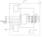
- FIG. 1Aschematically illustrates an exemplary memory module 10 compatible with certain embodiments described herein.
- the memory module 10is connectable to a computer system (not shown).
- the memory module 10comprises a printed circuit board 20 and a plurality of memory devices 30 coupled to the printed circuit board 20 .
- the plurality of memory devices 30has a first number of memory devices.
- the memory module 10further comprises a logic element 40 coupled to the printed circuit board 20 .
- the logic element 40receives a set of input control signals from the computer system.
- the set of input control signalscorrespond to a second number of memory devices smaller than the first number of memory devices.
- the logic element 40generates a set of output control signals in response to the set of input control signals.
- the set of output control signalscorresponds to the first number of memory devices.
- the memory module 10further comprises a phase-lock loop device 50 coupled to the printed circuit board 20 and a register 60 coupled to the printed circuit board 20 .
- the phase-lock loop device 50 and the register 60are each mounted on the printed circuit board 20 .
- the phase-lock loop device 50transmits clock signals to the plurality of memory devices 30 , the logic element 40 , and the register 60 .
- the register 60receives and buffers a plurality of control signals, including address signals (e.g., bank address signals, row address signals, column address signals, gated column address strobe signals, chip-select signals), and transmits corresponding signals to the appropriate memory devices 30 .
- address signalse.g., bank address signals, row address signals, column address signals, gated column address strobe signals, chip-select signals
- the register 60comprises a plurality of register devices. While the phase-lock loop device 50 , the register 60 , and the logic element 40 are described herein in certain embodiments as being separate components, in certain other embodiments, two or more of the phase-lock loop device 50 , the register 60 , and the logic element 40 are portions of a single component. Persons skilled in the art are able to select a phase-lock loop device 50 and a register 60 compatible with embodiments described herein.
- the memory module 10further comprises electrical components which are electrically coupled to one another and are surface-mounted or embedded on the printed circuit board 20 .
- electrical componentscan include, but are not limited to, electrical conduits, resistors, capacitors, inductors, and transistors. In certain embodiments, at least some of these electrical components are discrete, while in other certain embodiments, at least some of these electrical components are constituents of one or more integrated circuits.
- memory modules 10are compatible with embodiments described herein.
- memory modules 10 having memory capacities of 512-MB, 1-GB, 2-GB, 4-GB, 8-GB, as well as other capacities,are compatible with embodiments described herein.
- memory modules 10 having widths of 4 bytes, 8 bytes, 16 bytes, 32 bytes, or 32 bits, 64 bits, 128 bits, 256 bits, as well as other widths (in bytes or in bits),are compatible with embodiments described herein.
- memory modules 10 compatible with embodiments described hereininclude, but are not limited to, single in-line memory modules (SIMMs), dual in-line memory modules (DIMMs), small-outline DIMMs (SO-DIMMs), unbuffered DIMMs (UDIMMs), registered DIMMs (RDIMMs), fully-buffered DIMM (FBDIMM), mini-DIMMs, and micro-DIMMs.
- SIMMssingle in-line memory modules
- DIMMsdual in-line memory modules
- SO-DIMMssmall-outline DIMMs
- UDIMMsunbuffered DIMMs
- RDIMMsregistered DIMMs
- BCDIMMfully-buffered DIMM
- mini-DIMMsmini-DIMMs
- micro-DIMMsmicro-DIMMs.
- the printed circuit board 20is mountable in a module slot of the computer system.
- the printed circuit board 20 of certain such embodimentshas a plurality of edge connections electrically coupled to corresponding contacts of the module slot and to the various components of the memory module 10 , thereby providing electrical connections between the computer system and the components of the memory module 10 .
- Memory devices 30 compatible with embodiments described hereininclude, but are not limited to, random-access memory (RAM), dynamic random-access memory (DRAM), synchronous DRAM (SDRAM), and double-data-rate DRAM (e.g., DDR-1, DDR-2, DDR-3).
- RAMrandom-access memory
- DRAMdynamic random-access memory
- SDRAMsynchronous DRAM
- double-data-rate DRAMdouble-data-rate DRAM
- memory devices 30 having bit widths of 4, 8, 16, 32, as well as other bit widthsare compatible with embodiments described herein.
- Memory devices 30 compatible with embodiments described hereinhave packaging which include, but are not limited to, thin small-outline package (TSOP), ball-grid-array (BGA), fine-pitch BGA (FBGA), micro-BGA ( ⁇ BGA), mini-BGA (mBGA), and chip-scale packaging (CSP).
- TSOPthin small-outline package
- BGAball-grid-array
- FBGAfine-pitch BGA
- Memory devices 30 compatible with embodiments described hereinare available from a number of sources, including but not limited to, Samsung Semiconductor, Inc. of San Jose, Calif., Infineon Technologies AG of San Jose, Calif., and Micron Technology, Inc. of Boise, Id. Persons skilled in the art can select appropriate memory devices 30 in accordance with certain embodiments described herein.
- the plurality of memory devices 30are arranged in a first number of ranks.
- the memory devices 30are arranged in four ranks, as schematically illustrated by FIG. 1A .
- the memory devices 30are arranged in two ranks, as schematically illustrated by FIG. 1B .
- Other numbers of ranks of the memory devices 30are also compatible with embodiments described herein.
- the logic element 40comprises a programmable-logic device (PLD), an application-specific integrated circuit (ASIC), a field-programmable gate array (FPGA), a custom-designed semiconductor device, or a complex programmable-logic device (CPLD).
- the logic element 40is a custom device.
- Sources of logic elements 40 compatible with embodiments described hereininclude, but are not limited to, Lattice Semiconductor Corporation of Hillsboro, Oreg., Altera Corporation of San Jose, Calif., and Xilinx Incorporated of San Jose, Calif.
- the logic element 40comprises various discrete electrical elements, while in certain other embodiments, the logic element 40 comprises one or more integrated circuits. Persons skilled in the art can select an appropriate logic element 40 in accordance with certain embodiments described herein.
- the logic element 40receives a set of input control signals, which includes address signals (e.g., bank address signals, row address signals, column address signals, gated column address strobe signals, chip-select signals) and command signals (e.g., refresh, precharge) from the computer system.
- address signalse.g., bank address signals, row address signals, column address signals, gated column address strobe signals, chip-select signals
- command signalse.g., refresh, precharge
- the set of output control signalscorresponds to a first number of ranks in which the plurality of memory devices 30 of the memory module 10 are arranged
- the set of input control signalscorresponds to a second number of ranks per memory module for which the computer system is configured.
- the second number of ranksin certain embodiments is smaller than the first number of ranks.
- the first number of ranksis four while the second number of ranks is two.
- the first number of ranksis two while the second number of ranks is one.
- the memory module 10simulates a virtual memory module by operating as having the second number of ranks of memory devices 30 .
- the memory module 10simulates a virtual memory module when the number of memory devices 30 of the memory module 10 is larger than the number of memory devices 30 per memory module for which the computer system is configured to utilize.
- the computer systemis configured for a number of ranks per memory module which is smaller than the number of ranks in which the memory devices 30 of the memory module 10 are arranged.
- the computer systemis configured for two ranks of memory per memory module (providing two chip-select signals CS 0 , CS 1 ) and the plurality of memory modules 30 of the memory module 10 are arranged in four ranks, as schematically illustrated by FIG. 1A .
- the computer systemis configured for one rank of memory per memory module (providing one chip-select signal CS 0 ) and the plurality of memory modules 30 of the memory module 10 are arranged in two ranks, as schematically illustrated by FIG. 1B .
- the memory module 10has four ranks of memory devices 30 and the computer system is configured for two ranks of memory devices per memory module.
- the memory module 10receives row/column address signals or signal bits (A 0 -A n+1 ), bank address signals (BA 0 -BA m ), chip-select signals (CS 0 and CS 1 ), and command signals (e.g., refresh, precharge, etc.) from the computer system.
- the A 0 -A n row/column address signalsare received by the register 60 , which buffers these address signals and sends these address signals to the appropriate ranks of memory devices 30 .
- the logic element 40receives the two chip-select signals (CS 0 , CS 1 ) and one row/column address signal (A n+1 ) from the computer system. Both the logic element 40 and the register 60 receive the bank address signals (BA 0 -BA m ) and at least one command signal (e.g., refresh, precharge, etc.) from the computer system.
- Table 1provides a logic table compatible with certain embodiments described herein for the selection among ranks of memory devices 30 using chip-select signals. TABLE 1 State CS 0 CS 1 A n+1 Command CS 0A CS 0B CS 1A CS 1B 1 0 1 0 Active 0 1 1 1 2 0 1 1 Active 1 0 1 1 3 0 1 x Active 0 0 1 1 4 1 0 0 Active 1 1 0 1 5 1 0 1 Active 1 1 1 0 6 1 0 x Active 1 1 0 0 7 1 1 x x 1 1 1 1 1 Note: 1.
- Cs 0 , CS 1 , CS 0A , CS 0B , CS 1A , and CS 1Bare active low signals.
- a n+1is an active high signal.
- ‘x’is a Don't Care condition.
- Commandinvolves a number of command signals that define operations such as refresh, precharge, and other operations.
- CS 0is active low, A n+1 is non-active, and Command is active. CS 0A is pulled low, thereby selecting Rank 0.
- CS 0is active low
- a n+1is Don't Care
- Commandis active high
- CS 0A and CS 0Bare pulled low, thereby selecting Ranks 0 and 1.
- CS 1is active low, A n+1 is non-active, and Command is active. CS 1A is pulled low, thereby selecting Rank 2.
- CS 1is active low
- a n+1is Don't Care
- Commandis active.
- CS 1A and CS 1Bare pulled low, thereby selecting Ranks 2 and 3.
- CS 0 and CS 1are pulled non-active high, which deselects all ranks, i.e., CS 0A , CS 0B , CS 1A , and CS 1B are pulled high.
- the “Command” column of Table 1represents the various commands that a memory device (e.g., a DRAM device) can execute, examples of which include, but are not limited to, activation, read, write, precharge, and refresh.
- the command signalis passed through to the selected rank only (e.g., state 4 of Table 1).
- the command signal(e.g., read) is sent to only one memory device or the other memory device so that data is supplied from one memory device at a time.
- the command signalis passed through to both associated ranks (e.g., state 6 of Table 1).
- the command signale.g., refresh
- Certain embodimentsutilize a logic table such as that of Table 1 to simulate a single memory device from two memory devices by selecting two ranks concurrently.
- Table 2provides a logic table compatible with certain embodiments described herein for the selection among ranks of memory devices 30 using gated CAS signals.
- CS* RAS* CAS* WE* Density BitA 10 Command CAS0* CAS1* 1 x x x x x x NOP x x 0 1 1 1 x x NOP 1 1 0 0 1 1 0 x ACTIVATE 1 1 0 0 1 1 1 x ACTIVATE 1 1 0 1 0 1 0 1 0 x READ 0 1 0 1 0 1 1 1 x READ 1 0 0 1 0 0 0 x WRITE 0 1 0 1 0 1 0 1 0 0 1 x WRITE 1 0 0 0 1 0 0 0 PRECHARGE 1 1 0 0 1 0 1 0 PRECHARGE 1 1 0 0 1 0 0 0 x 1 PRECHARGE 1 1 0 0 0 0 x
- the density bitis the value latched during the activate command for the selected bank.
- Serial-presence detect (SPD) device 70e.g., an electrically-erasable-programmable read-only memory or EEPROM device
- SPDserial-presence detect
- the SPD device 70communicates this data to the basic input/output system (BIOS) of the computer system so that the computer system is informed of the memory capacity and the memory configuration available for use and can configure the memory controller properly for maximum reliability and performance.
- BIOSbasic input/output system
- the SPD devicecontains the following SPD data (in appropriate bit fields of these bytes):
- the SPD devicecontains the following SPD data (in appropriate bit fields of these bytes):
- the SPD device 70comprises data which characterize the memory module 10 as having fewer ranks of memory devices than the memory module 10 actually has, with each of these ranks having more memory density. For example, for a memory module 10 compatible with certain embodiments described herein having two ranks of memory devices 30 , the SPD device 70 comprises data which characterizes the memory module 10 as having one rank of memory devices with twice the memory density per rank. Similarly, for a memory module 10 compatible with certain embodiments described herein having four ranks of memory devices 30 , the SPD device 70 comprises data which characterizes the memory module 10 as having two ranks of memory devices with twice the memory density per rank.
- the SPD device 70comprises data which characterize the memory module 10 as having fewer memory devices than the memory module 10 actually has, with each of these memory devices having more memory density per memory device.
- the SPD device 70comprises data which characterizes the memory module 10 as having one-half the number of memory devices that the memory module 10 actually has, with each of these memory devices having twice the memory density per memory device.
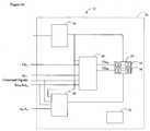
- FIG. 1Cschematically illustrates an exemplary memory module 10 in accordance with certain embodiments described herein.
- the memory module 10comprises a pair of substantially identical memory devices 31 , 33 .
- Each memory device 31 , 33has a first bit width, a first number of banks of memory locations, a first number of rows of memory locations, and a first number of columns of memory locations.
- the memory module 10further comprises an SPD device 70 comprising data that characterizes the pair of memory devices 31 , 33 .
- the datacharacterize the pair of memory devices 31 , 33 as a virtual memory device having a second bit width equal to twice the first bit width, a second number of banks of memory locations equal to the first number of banks, a second number of rows of memory locations equal to the first number of rows, and a second number of columns of memory locations equal to the first number of columns.
- the SPD device 70 of the memory module 10is programmed to describe the combined pair of lower-density memory devices 31 , 33 as one virtual or pseudo-higher-density memory device.
- two 512-Mb memory devices, each with a 128M ⁇ 4-bit configuration,are used to simulate one 1-Gb memory device having a 128M ⁇ 8-bit configuration.
- the SPD device 70 of the memory module 10is programmed to describe the pair of 512-Mb memory devices as one virtual or pseudo-1-Gb memory device.
- sixteen 512-Mb (128M ⁇ 4-bit) memory devicescan be used.
- the sixteen 512-Mb (128M ⁇ 4-bit) memory devicesare combined in eight pairs, with each pair serving as a virtual or pseudo-1-Gb (128M ⁇ 8-bit) memory device.
- the SPD device 70contains the following SPD data (in appropriate bit fields of these bytes):
- bytes 3 , 4 , and 17are programmed to have the same values as they would have for a 512-MB (128M ⁇ 4-byte) memory module utilizing 512-Mb (128M ⁇ 4-bit) memory devices.
- bytes 13 and 14 of the SPD dataare programmed to be equal to 8, corresponding to the bit width of the virtual or pseudo-higher-density 1-Gb (128M ⁇ 8-bit) memory device, for a total capacity of 1-GB.
- the SPD datadoes not describe the actual-lower-density memory devices, but instead describes the virtual or pseudo-higher-density memory devices.
- the BIOSaccesses the SPD data and recognizes the memory module as having 4 banks of memory locations arranged in 2 13 rows and 2 12 columns, with each memory location having a width of 8 bits rather than 4 bits.
- the computer system's memory controllerwhen such a memory module 10 is inserted in a computer system, the computer system's memory controller then provides to the memory module 10 a set of input control signals which correspond to the number of ranks or the number of memory devices reported by the SPD device 70 .
- the SPD device 70reports to the computer system that the memory module 10 only has one rank.
- the logic element 40then receives a set of input control signals corresponding to a single rank from the computer system's memory controller, and generates and transmits a set of output control signals corresponding to two ranks to the appropriate memory devices 30 of the memory module 10 .
- a two-rank memory module 10 compatible with certain embodiments described hereinwhen a two-rank memory module 10 compatible with certain embodiments described herein is placed in a computer system compatible with either one- or two-rank memory modules, the SPD device 70 reports to the computer system that the memory module 10 only has one rank.
- the logic element 40receives a set of input control signals corresponding to a single rank from the computer system's memory controller, and generates and transmits a set of output control signals corresponding to two ranks to the appropriate memory devices 30 of the memory module 10 .
- a four-rank memory module 10 compatible with certain embodiments described hereinsimulates a two-rank memory module whether the memory module 10 is inserted in a computer system compatible with two-rank memory modules or with two- or four-rank memory modules.
- the computer systemprovides four chip-select signals, but the memory module 10 only uses two of the chip-select signals.
- two memory devices having a memory densityare used to simulate a single memory device having twice the memory density, and an additional address signal bit is used to access the additional memory.
- two ranks of memory devices having a memory densityare used to simulate a single rank of memory devices having twice the memory density, and an additional address signal bit is used to access the additional memory.
- such simulations of memory devices or ranks of memory devicesare termed as “memory density multiplication,” and the term “density transition bit” is used to refer to the additional address signal bit which is used to access the additional memory.
- the memory module 10can have various types of memory devices 30 (e.g., DDR1, DDR2, DDR3, and beyond).
- the logic element 40 of certain such embodimentsutilizes implied translation logic equations having variations depending on whether the density transition bit is a row, column, or internal bank address bit.
- the translation logic equations of certain embodimentsvary depending on the type of memory module 10 (e.g., UDIMM, RDIMM, FBDIMM, etc.).
- the translation logic equationsvary depending on whether the implementation multiplies memory devices per rank or multiplies the number of ranks per memory module.
- Table 3Aprovides the numbers of rows and columns for DDR-1 memory devices, as specified by JEDEC standard JESD79D, “Double Data Rate (DDR) SDRAM Specification,” published February 2004, and incorporated in its entirety by reference herein.
- TABLE 3A128-Mb 256-Mb 512-Mb 1-Gb Number of banks 4 4 4 4 Number of row address bits 12 13 13 14 Number of column address bits for 11 11 12 12 “ ⁇ 4” configuration Number of column address bits for 10 10 11 11 “ ⁇ 8” configuration Number of column address bits for 9 9 10 10 “ ⁇ 16” configuration
- 512-Mb (128M ⁇ 4-bit) DRAM deviceshave 2 13 rows and 2 12 columns of memory locations, while 1-Gb (128M ⁇ 8-bit) DRAM devices have 2 14 rows and 2 11 columns of memory locations. Because of the differences in the number of rows and the number of columns for the two types of memory devices, complex address translation procedures and structures would typically be needed to fabricate a 1-GB (128M ⁇ 8-byte) memory module using sixteen 512-Mb (128M ⁇ 4-bit) DRAM devices.
- Table 3Bshows the device configurations as a function of memory density for DDR2 memory devices. TABLE 3B Number of Number of Number of Page Size Rows Columns Internal Banks ( ⁇ 4s or ⁇ 8s) 256 Mb 13 10 4 1 KB 512 Mb 14 10 4 1 KB 1 Gb 14 10 8 1 KB 2 Gb 15 10 8 1 KB 4 Gb to be to be 8 1 KB determined determined
- Table 4lists the corresponding density transition bit for the density transitions between the DDR2 memory densities of Table 3B. TABLE 4 Density Transition Density Transition Bit 256 Mb to 512 Mb A 13 512 Mb to 1 Gb BA 2 1 Gb to 2 Gb A 14 2 Gb to 4 Gb to be determined Because the standard memory configuration of 4-Gb DDR2 SDRAM modules is not yet determined by the appropriate standards-setting organization, Tables 3B and 4 have “to be determined” in the appropriate table entries.
- the logic translation equationsare programmed in the logic element 40 by hardware, while in certain other embodiments, the logic translation equations are programmed in the logic element 40 by software.
- Examples 1 and 2provide exemplary sections of Verilog code compatible with certain embodiments described herein. As described more fully below, the code of Examples 1 and 2 includes logic to reduce potential problems due to “back-to-back adjacent read commands which cross memory device boundaries or “BBARX.” Persons skilled in the art are able to provide additional logic translation equations compatible with embodiments described herein.
- Example 1An exemplary section of Verilog code compatible with memory density multiplication from 512 Mb to 1 Gb using DDR2 memory devices with the BA 2 density transition bit is listed below in Example 1.
- the exemplary code of Example 1corresponds to a logic element 40 which receives one chip-select signal from the computer system and which generates two chip-select signals.
- Example 2Another exemplary section of Verilog code compatible with memory density multiplication from 256 Mb to 512 Mb using DDR2 memory devices and gated CAS signals with the row A 13 density transition bit is listed below in Example 2.
- the exemplary code of Example 2corresponds to a logic element 40 which receives one gated CAS signal from the computer system and which generates two gated CAS signals.
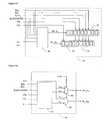
- FIG. 2Aschematically illustrates an exemplary memory module 10 which doubles the rank density in accordance with certain embodiments described herein.
- the memory module 10has a first memory capacity.
- the memory module 10comprises a plurality of substantially identical memory devices 30 configured as a first rank 32 and a second rank 34 .
- the memory devices 30 of the first rank 32are configured in pairs, and the memory devices 30 of the second rank 34 are also configured in pairs.
- the memory devices 30 of the first rank 32are configured with their respective DQS pins tied together and the memory devices 30 of the second rank 34 are configured with their respective DQS pins tied together, as described more fully below.
- the memory module 10further comprises a logic element 40 which receives a first set of address and control signals from a memory controller (not shown) of the computer system.
- the first set of address and control signalsis compatible with a second memory capacity substantially equal to one-half of the first memory capacity.
- the logic element 40translates the first set of address and control signals into a second set of address and control signals which is compatible with the first memory capacity of the memory module 10 and which is transmitted to the first rank 32 and the second rank 34 .
- the first rank 32 of FIG. 2Ahas 18 memory devices 30 and the second rank 34 of FIG. 2A has 18 memory devices 30 .
- Other numbers of memory devices 30 in each of the ranks 32 , 34are also compatible with embodiments described herein.
- the memory module 10has a width of 8 bytes (or 64 bits) and each of the memory devices 30 of FIG. 2A has a bit width of 4 bits.
- the 4-bit-wide (“ ⁇ 4”) memory devices 30 of FIG. 2Ahave one-half the width, but twice the depth of 8-bit-wide (“ ⁇ 8”) memory devices.
- each pair of “ ⁇ 4” memory devices 30has the same density as a single “ ⁇ 8” memory device, and pairs of “ ⁇ 4” memory devices 30 can be used instead of individual “ ⁇ 8” memory devices to provide the memory density of the memory module 10 .
- a pair of 512-Mb 128M ⁇ 4-bit memory deviceshas the same memory density as a 1-Gb 128M ⁇ 8-bit memory device.
- the relative DQS pins of the two memory devices 30are advantageously tied together, as described more fully below.
- an additional address lineis used to access the memory density of a high-density memory module 10 comprising pairs of “ ⁇ 4” memory devices 30 . While a high-density memory module comprising individual “ ⁇ 8” memory devices with the next-higher density would also utilize an additional address line, the additional address lines are different in the two memory module configurations.
- a 1-Gb 128M ⁇ 8-bit DDR-1 DRAM memory deviceuses row addresses A 13 -A 0 and column addresses A 11 and A 0 -A 0 .
- a pair of 512-Mb 128M ⁇ 4-bit DDR-1 DRAM memory devicesuses row addresses A 12 -A 0 and column addresses A 12 , A 11 , and A 9 -A 0 .
- a memory controller of a computer system utilizing a 1-GB 128M ⁇ 8 memory module 10 comprising pairs of the 512-Mb 128M ⁇ 4 memory devices 30supplies the address and control signals including the extra row address (A 13 ) to the memory module 10 .
- the logic element 40receives the address and control signals from the memory controller and converts the extra row address (A 13 ) into an extra column address (A 12 ).
- FIG. 2Bschematically illustrates an exemplary logic element 40 compatible with embodiments described herein.
- the logic element 40is used for a memory module 10 comprising pairs of “ ⁇ 4” memory devices 30 which mimic individual “ ⁇ 8” memory devices. In certain embodiments, each pair has the respective DQS pins of the memory devices 30 tied together.
- the logic element 40comprises a programmable-logic device (PLD) 42 , a first multiplexer 44 electrically coupled to the first rank 32 of memory devices 30 , and a second multiplexer 46 electrically coupled to the second rank 34 of memory devices 30 .
- PLDprogrammable-logic device
- the PLD 42 and the first and second multiplexers 44 , 46are discrete elements, while in, other certain embodiments, they are integrated within a single integrated circuit. Persons skilled in the art can select an appropriate PLD 42 , first multiplexer 44 , and second multiplexer 46 in accordance with embodiments described herein.
- the first multiplexer 44passes the A 12 address through to the first rank 32
- the second multiplexer 46passes the A 12 address through to the second rank 34
- the PLD 42saves or latches the A 13 address from the memory controller.
- a copy of the A 13 addressis saved by the PLD 42 for each of the internal banks (e.g., 4 internal banks) per memory device 30 .
- the first multiplexer 44passes the previously-saved A 13 address through to the first rank 32 as the A 12 address and the second multiplexer 46 passes the previously-saved A 13 address through to the second rank 34 as the A 12 address.
- the first rank 32 and the second rank 34thus interpret the previously-saved A 13 row address as the current A 12 column address.
- the logic element 40translates the extra row address into an extra column address in accordance with certain embodiments described herein.
- certain embodiments described hereinprovide the advantage of using lower-cost, lower-density memory devices to build “next-generation” higher-density memory modules. Certain embodiments advantageously allow the use of lower-cost readily-available 512-Mb DDR-2 SDRAM devices to replace more expensive 1-Gb DDR-2 SDRAM devices. Certain embodiments advantageously reduce the total cost of the resultant memory module.
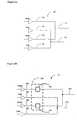
- FIG. 3Aschematically illustrates an exemplary memory module 10 which doubles number of ranks in accordance with certain embodiments described herein.
- the memory module 10has a first plurality of memory locations with a first memory density.
- the memory module 10comprises a plurality of substantially identical memory devices 30 configured as a first rank 32 , a second rank 34 , a third rank 36 , and a fourth rank 38 .
- the memory module 10further comprises a logic element 40 which receives a first set of address and control signals from a memory controller (not shown).
- the first set of address and control signalsis compatible with a second plurality of memory locations having a second memory density.
- the second memory densityis substantially equal to one-half of the first memory density.
- the logic element 40translates the first set of address and control signals into a second set of address and control signals which is compatible with the first plurality of memory locations of the memory module 10 and which is transmitted to the first rank 32 , the second rank 34 , the third rank 36 , and the fourth rank 38 .
- Each rank 32 , 34 , 36 , 38 of FIG. 3Ahas 9 memory devices 30 .
- Other numbers of memory devices 30 in each of the ranks 32 , 34 , 36 , 38are also compatible with embodiments described herein.
- the memory module 10has a width of 8 bytes (or 64 bits) and each of the memory devices 30 of FIG. 3A has a bit width of 8 bits. Because the memory module 10 has twice the number of 8-bit-wide (“ ⁇ 8”) memory devices 30 as does a standard 8-byte-wide memory module, the memory module 10 has twice the density as does a standard 8-byte-wide memory module. For example, a 1-GB 128M ⁇ 8-byte memory module with 36 512-Mb 128M ⁇ 8-bit memory devices (arranged in four ranks) has twice the memory density as a 512-Mb 128M ⁇ 8-byte memory module with 18 512-Mb 128M ⁇ 8-bit memory devices (arranged in two ranks).
- the two chip-select signals(CS 0 , CS 1 ) are used with other address and control signals to gate a set of four gated CAS signals.
- the CS 0 and CS 1 signalsalong with the other address and control signals are used to gate the CAS signal appropriately, as schematically illustrated by FIG. 3A .
- FIG. 3Bschematically illustrates an exemplary logic element 40 compatible with embodiments described herein.
- the logic element 40comprises a programmable-logic device (PLD) 42 and four “OR” logic elements 52 , 54 , 56 , 58 electrically coupled to corresponding ranks 32 , 34 , 36 , 38 of memory devices 30 .
- PLDprogrammable-logic device
- the PLD 42comprises an ASIC, an FPGA, a custom-designed semiconductor device, or a CPLD.
- the PLD 42 and the four “OR” logic elements 52 , 54 , 56 , 58are discrete elements, while in other certain embodiments, they are integrated within a single integrated circuit. Persons skilled in the art can select an appropriate PLD 42 and appropriate “OR” logic elements 52 , 54 , 56 , 58 in accordance with embodiments described herein.
- the PLD 42transmits each of the four “enabled CAS” (ENCAS 0 a, ENCAS 0 b, ENCAS 1 a, ENCAS 1 b) signals to a corresponding one of the “OR” logic elements 52 , 54 , 56 , 58 .
- the CAS signalis also transmitted to each of the four “OR” logic elements 52 , 54 , 56 , 58 .
- the CAS signal and the “enabled CAS” signalsare “low” true signals.
- the PLD 42By selectively activating each of the four “enabled CAS” signals which are inputted into the four “OR” logic elements 52 , 54 , 56 , 58 , the PLD 42 is able to select which of the four ranks 32 , 34 , 36 , 38 is active.
- the PLD 42uses sequential and combinatorial logic procedures to produce the gated CAS signals which are each transmitted to a corresponding one of the four ranks 32 , 34 , 36 , 38 .
- the PLD 42instead uses sequential and combinatorial logic procedures to produce four gated chip-select signals (e.g., CS 0 a, CS 0 b, CS 1 a, and CS 1 b) which are each transmitted to a corresponding one of the four ranks 32 , 34 , 36 , 38 .
- DDR SDRAMe.g., DDR1, DDR2, DDR3 memory devices operate with a data transfer protocol which surrounds each burst of data strobes with a pre-amble time interval and a post-amble time interval.
- the pre-amble time intervalprovides a timing window for the receiving memory device to enable its data capture circuitry when a known valid level is present on the strobe signal to avoid false triggers of the memory device's capture circuit.
- the post-amble time intervalprovides extra time after the last strobe for this data capture to facilitate good signal integrity.
- FIG. 4Ashows an exemplary timing diagram of this “gapless” read burst for a back-to-back adjacent read condition from one memory device.
- the second read commandaccesses data from a different memory device than does the first read command
- there is at least one time intervale.g., clock cycle
- This inserted time intervalallows both read data bursts to occur without the post-amble time interval of the first read data burst colliding or otherwise interfering with the pre-amble time interval of the second read data burst.
- the memory controller of the computer systeminserts an extra clock cycle between successive read commands issued to different memory devices, as shown in the exemplary timing diagram of FIG. 4B for successive read accesses from different memory devices.
- the memory controlleris informed of the memory boundaries between the ranks of memory of the memory module prior to issuing read commands to the memory module.
- Such memory controllerscan insert wait time intervals or clock cycles to avoid collisions or interference between back-to-back adjacent read commands which cross memory device boundaries, which are referred to herein as “BBARX.”
- the logic element 40In certain embodiments described herein in which the number of ranks of the memory module is doubled or quadrupled, the logic element 40 generates a set of output control signals so that the selection decoding is transparent to the computer system. However, in certain such embodiments, there are memory device boundaries of which the computer system is unaware, so there are occasions in which BBARX occurs without the cognizance of the memory controller of the computer system. As shown in FIG. 5 , the last data strobe of memory device “a” collides with the pre-amble time interval of the data strobe of memory device “b,” resulting in a “collision window.”
- FIG. 6Aschematically illustrates a circuit diagram of a conventional memory module 100 showing the interconnections between the DQ data signal lines 102 of the memory devices “a” and “b” (not shown) and their DQS data strobe signal lines 104 .
- the electrical signal linesare etched on the printed circuit board.
- each of the memory deviceshas their DQ data signal lines 102 electrically coupled to a common DQ line 112 and the DQS data strobe signal lines 104 electrically coupled to a common DQS line 114 .
- FIG. 6Bschematically illustrates a circuit diagram of an exemplary memory module 10 comprising an isolation device 120 in accordance with certain embodiments described herein.
- each of the memory devices 30 otherwise involved in a BBARX collisionhave their DQS data strobe signal lines 104 electrically coupled to the common DQS line 114 through the isolation element 120 .
- the isolation device 120of certain embodiments multiplexes the DQS data strobe signal lines 104 of the two ranks of memory devices 30 from one another to avoid a BBARX collision.
- the isolation device 120comprises a first switch 122 electrically coupled to a first data strobe signal line (e.g., DQSa) of a first memory device (not shown) and a second switch 124 electrically coupled to a second data strobe signal line (e.g., DQSb) of a second memory device (not shown).
- exemplary switches compatible with embodiments described hereininclude, but are not limited to field-effect transistor (FET) switches, such as the SN74AUC1G66 single bilateral analog switch available from Texas Instruments, Inc. of Dallas, Tex.
- FETfield-effect transistor
- the time for switching the first switch 122 and the second switch 124is between the two read data bursts (e.g., after the last DQS data strobe of the read data burst of the first memory device and before the first DQS data strobe of the read data burst of the second memory device).
- the first switch 122is enabled.
- the first switch 122is disabled and the second switch 124 is enabled.
- the isolation device 120comprises a logic element 140 which multiplexes the DQS data strobe signal lines 104 from one another.
- Exemplary logic elements compatible with embodiments described hereininclude, but are not limited to multiplexers, such as the SN74AUC2G53 2:1 analog multiplexer/demultiplexer available from Texas Instruments, Inc. of Dallas, Tex.
- the logic element 140receives a first DQS data strobe signal from the first memory device and a second DQS data strobe signal from a second memory device and selectively switches one of the first and second DQS data strobe signals to the common DQS data strobe signal line 114 .
- Persons skilled in the artcan select other types of isolation devices 120 compatible with embodiments described herein.
- the isolation device 120also multiplexes the DQ data signal lines 102 of the two memory devices from one another.
- the isolation device 120comprises a pair of switches on the DQ data signal lines 102 , similar to the switches 122 , 124 on the DQS data strobe signal lines 104 schematically illustrated by FIG. 6B .
- the isolation device 120comprises a logic element 150 , as schematically illustrated by FIG. 6D .
- the same types of switches and/or logic elementsare used for the DQ data signal lines 102 as for the DQS data strobe signal lines 104 .
- the logic element 150receives a first DQ data signal from the first memory device and a second DQ data signal from the second memory device and selectively switches one of the first and second DQ data signals to the common DQ data signal line 112 .
- first DQ data signalfrom the first memory device
- second DQ data signalfrom the second memory device and selectively switches one of the first and second DQ data signals to the common DQ data signal line 112 .
- isolation devices 120can select other types of isolation devices 120 compatible with embodiments described herein.
- the isolation device 120advantageously adds propagation delays to the DQ data signals which match the DQS strobe signals being multiplexed by the isolation device 120 .
- the isolation device 120advantageously presents a reduced impedance load to the computer system by selectively switching between the two ranks of memory devices to which it is coupled. This feature of the isolation device 120 is used in certain embodiments in which there is no memory density multiplication of the memory module (e.g., for a computer system with four chip-select signals), but where the impedance load of the memory module may otherwise limit the number of ranks or the number of memory devices per memory module.
- the isolation device 120 of certain such embodimentscomprises the logic element 150 on the DQ data signal lines but not a corresponding logic element on the DQS data strobe signal lines.
- the control and timing of the isolation device 120is performed by an isolation-control logic element (e.g., application-specific integrated circuit, custom programmable logic device, field-programmable gate array, etc.) which is resident on the memory module 10 .
- the isolation-control logic elementis the same logic element 40 as schematically illustrated in FIGS. 1A and 1B , is part of the isolation device 120 (e.g., logic element 140 or logic element 150 as schematically illustrated by FIG. 6D ), or is a separate component.
- the isolation-control logic element of certain embodimentscontrols the isolation device 120 by monitoring commands received by the memory module 10 from the computer system and producing “windows” of operation whereby the appropriate components of the isolation device 120 are switched to enable and disable the DQS data strobe signal lines 104 to mitigate BBARX collisions.
- the isolation-control logic elementmonitors the commands received by the memory module from the computer system and selectively enables and disables the DQ data signal lines 102 to reduce the load impedance of the memory module 10 on the computer system. In still other embodiments, this logic element performs both of these functions together.
- the computer systemadvantageously recognizes a 1-GB memory module comprising 256-Mb memory devices with 64M ⁇ 4-bit configuration as a 1-GB memory module having 512-Mb memory devices with 64M ⁇ 8-bit configuration (e.g., as a 1-GB memory module with 128M ⁇ 8-byte configuration).
- This advantageous resultis desirably achieved in certain embodiments by electrically connecting together two output signal pins (e.g., DQS or data strobe pins) of the two 256-Mb memory devices such that both output signal pins are concurrently active when the two memory devices are concurrently enabled.
- the DQS or data strobeis a bi-directional signal that is used during both read cycles and write cycles to validate or latch data.
- the terms “tying together” or “tied together”refer to a configuration in which corresponding pins (e.g., DQS pins) of two memory devices are electrically connected together and are concurrently active when the two memory devices are concurrently enabled (e.g., by a common chip-select or CS signal).
- corresponding pinse.g., DQS pins
- CS signalcommon chip-select
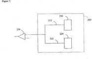
- FIGS. 7 and 8schematically illustrate a problem which may arise from tying together two output signal pins.
- FIG. 7schematically illustrates an exemplary memory module 205 in which a first DQS pin 212 of a first memory device 210 is electrically connected to a second DQS pin 222 of a second memory device 220 .
- the two DQS pins 212 , 222are both electrically connected to a memory controller 230 .
- FIG. 8is an exemplary timing diagram of the voltages applied to the two DQS pins 212 , 222 due to non-simultaneous switching.
- both the first DQS pin 212 and the second DQS pin 222are high, so no current flows between them.
- both the first DQS pin 212 and the second DQS pin 222are low, so no current flows between them.
- the first DQS pin 212is low while the second DQS pin 222 is high. Under such conditions, a current will flow between the two DQS pins 212 , 222 .
- This condition in which one DQS pin is low while the other DQS pin is highcan occur for fractions of a second (e.g., 0.8 nanoseconds) during the dynamic random-access memory (DRAM) read cycle.
- the current flowing between the two DQS pins 212 , 222can be substantial, resulting in heating of the memory devices 210 , 220 , and contributing to the degradation of reliability and eventual failure of these memory devices.
- FIG. 9schematically illustrates another exemplary memory module 205 in which a first DQS pin 212 of a first memory device 210 is electrically connected to a second DQS pin 214 of a second memory device 220 .
- the two DQS pins 212 , 214 of FIG. 9are both electrically connected to a memory controller (not shown).
- the DQ (data input/output) pin 222 of the first memory device 210 and the corresponding DQ pin 224 of the second memory device 220are each electrically connected to the memory controller by the DQ bus (not shown).
- each memory device 210 , 220will have a plurality of DQ pins (e.g., eight DQ pins per memory device), but for simplicity, FIG. 9 only shows one DQ pin for each memory device 210 , 220 .
- Each of the memory devices 210 , 220 of FIG. 9utilizes a respective on-die termination or “ODT” circuit 232 , 234 which has termination resistors (e.g., 75 ohms) internal to the memory devices 210 , 220 to provide signal termination.
- Each memory device 210 , 220has a corresponding ODT signal pin 262 , 264 which is electrically connected to the memory controller via an ODT bus 240 .
- the ODT signal pin 262 of the first memory device 210receives a signal from the ODT bus 240 and provides the signal to the ODT circuit 232 of the first memory device 210 .
- the ODT circuit 232responds to the signal by selectively enabling or disabling the internal termination resistors 252 , 256 of the first memory device 210 .
- This behavioris shown schematically in FIG. 9 by the switches 242 , 244 which are either closed (dash-dot line) or opened (solid line).
- the ODT signal pin 264 of the second memory device 220receives a signal from the ODT bus 240 and provides the signal to the ODT circuit 234 of the second memory device 220 .
- the ODT circuit 234responds to the signal by selectively enabling or disabling the internal termination resistors 254 , 258 of the second memory device 220 . This behavior is shown schematically in FIG.
- switches 246 , 248which are either closed (dash-dot line) or opened (solid line).
- the switches 242 , 244 , 246 , 248 of FIG. 9are schematic representations of the operation of the ODT circuits 232 , 234 , and do not signify that the ODT circuits 232 , 234 necessarily include mechanical switches.
- Examples of memory devices 210 , 220 which include such ODT circuits 232 , 234include, but are not limited to, DDR2 memory devices. Such memory devices are configured to selectively enable or disable the termination of the memory device in this way in response to signals applied to the ODT signal pin of the memory device. For example, when the ODT signal pin 262 of the first memory device 210 is pulled high, the termination resistors 252 , 256 of the first memory device 210 are enabled. When the ODT signal pin 262 of the first memory device 210 is pulled low (e.g., grounded), the termination resistors 252 , 256 of the first memory device 210 are disabled.
- the DQS pins 212 , 214 of each memory device 210 , 220are selectively connected to a voltage VTT through a corresponding termination resistor 252 , 254 internal to the corresponding memory device 210 , 220 .
- the DQ pins 222 , 224are selectively connected to a voltage VTT through a corresponding termination resistor 256 , 258 internal to the corresponding memory device 210 , 220 .
- the DQ pins 212 , 214 and/or the DQS pins 222 , 224are selectively connected to ground through the corresponding termination resistors 252 , 254 , 256 , 258 .
- the resistances of the internal termination resistors 252 , 254 , 256 , 258are selected to clamp the voltages so as to reduce the signal reflections from the corresponding pins.
- each internal termination resistor 252 , 254 , 256 , 258has a resistance of approximately 75 ohms.
- both the first memory device 210 and the second memory device 220are enabled at the same time (e.g., by a common CS signal). Connecting the first memory device 210 and the second memory device 220 by tying the DQS pins 212 , 214 together, as shown in FIG. 9 , results in a reduced effective termination resistance for the DQS pins 212 , 214 .
- FIG. 9For example, for the exemplary configuration of FIG.
- the effective termination resistance for the DQS pins 212 , 214is approximately 37.5 ohms, which is one-half the desired ODT resistance (for 75-ohm internal termination resistors) to reduce signal reflections since the internal termination resistors 252 , 254 of the two memory devices 210 , 220 are connected in parallel. This reduction in the termination resistance can result in signal reflections causing the memory device to malfunction.
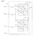
- FIG. 10schematically illustrates an exemplary memory module 300 in accordance with certain embodiments described herein.
- the memory module 300comprises a first memory device 310 having a first data strobe (DQS) pin 312 and a second memory device 320 having a second data strobe (DQS) pin 322 .
- the memory module 300further comprises a first resistor 330 electrically coupled to the first DQS pin 312 .
- the memory module 300further comprises a second resistor 340 electrically coupled to the second DQS pin 322 and to the first resistor 330 .
- the first DQS pin 312is electrically coupled to the second DQS pin 322 through the first resistor 330 and through the second resistor 340 .
- the memory module 300is a 1-GB unbuffered Double Data Rate (DDR) Synchronous Dynamic RAM (SDRAM) high-density dual in-line memory module (DIMM).
- FIGS. 11A and 11Bschematically illustrate a first side 362 and a second side 364 , respectively, of such a memory module 300 with eighteen 64M ⁇ 4-bit, DDR-1 SDRAM FBGA memory devices on each side of a 184-pin glass-epoxy printed circuit board (PCB) 360 .
- DDRDouble Data Rate
- SDRAMSynchronous Dynamic RAM
- DIMMhigh-density dual in-line memory module
- the memory module 300further comprises a phase-lock-loop (PLL) clock driver 370 , an EEPROM for serial-presence detect (SPD) data 380 , and decoupling capacitors (not shown) mounted on the PCB in parallel to suppress switching noise on VDD and VDDQ power supply for DDR-1 SDRAM.
- PLLphase-lock-loop
- SPDserial-presence detect
- decoupling capacitorsmounted on the PCB in parallel to suppress switching noise on VDD and VDDQ power supply for DDR-1 SDRAM.
- the memory module 300comprises a plurality of memory devices configured in pairs, each pair having a first memory device 310 and a second memory device 320 .
- a 128M ⁇ 72-bit DDR SDRAM high-density memory module 300comprises thirty-six 64M ⁇ 4-bit DDR-1 SDRAM integrated circuits in FBGA packages configured in eighteen pairs.
- the first memory device 310 of each pairhas the first DQS pin 312 electrically coupled to the second DQS pin 322 of the second memory device 320 of the pair.
- the first DQS pin 312 and the second DQS pin 322are concurrently active when the first memory device 310 and the second memory device 320 are concurrently enabled.
- the first resistor 330 and the second resistor 340each has a resistance advantageously selected to reduce the current flow between the first DQS pin 312 and the second DQS pin 322 while allowing signals to propagate between the memory controller and the DQS pins 312 , 322 .
- each of the first resistor 330 and the second resistor 340has a resistance in a range between approximately 5 ohms and approximately 50 ohms.
- each of the first resistor 330 and the second resistor 340has a resistance of approximately 22 ohms.
- Other resistance values for the first resistor 330 and the second resistor 340are also compatible with embodiments described herein.
- the first resistor 330comprises a single resistor, while in other embodiments, the first resistor 330 comprises a plurality of resistors electrically coupled together in series and/or in parallel.
- the second resistor 340comprises a single resistor, while in other embodiments, the second resistor 340 comprises a plurality of resistors electrically coupled together in series and/or in parallel.
- FIGS. 12A and 12Bschematically illustrate an exemplary embodiment of a memory module 300 in which the first resistor 330 and the second resistor 340 are used to reduce the current flow between the first DQS pin 312 and the second DQS pin 322 .
- the memory module 300is part of a computer system 400 having a memory controller 410 .
- the first resistor 330has a resistance of approximately 22 ohms and the second resistor 340 has a resistance of approximately 22 ohms.
- the first resistor 330 and the second resistor 340are electrically coupled in parallel to the memory controller 410 through a signal line 420 having a resistance of approximately 25 ohms.
- the first resistor 330 and the second resistor 340are also electrically coupled in parallel to a source of a fixed termination voltage (identified by VTT in FIGS. 12A and 12B ) by a signal line 440 having a resistance of approximately 47 ohms.
- a source of a fixed termination voltageidentified by VTT in FIGS. 12A and 12B
- a signal line 440 having a resistance of approximately 47 ohmsSuch an embodiment can advantageously be used to allow two memory devices having lower bit widths (e.g., 4-bit) to behave as a single virtual memory device having a higher bit width (e.g., 8-bit).
- FIG. 12Bschematically illustrates exemplary current-limiting resistors 330 , 340 in conjunction with the impedances of the memory devices 310 , 320 .
- the memory controller 410is in a high-impedance condition
- the first memory device 310drives the first DQS pin 312 high (e.g., 2.7 volts)
- the second memory device 320drives the second DQS pin 322 low (e.g., 0 volts).
- the amount of time for which this condition occursis approximated by the time between t 2 and t 3 of FIG.
- the DQS driver of the first memory device 310has a driver impedance R 1 of approximately 17 ohms
- the DQS driver of the second memory device 320has a driver impedance R 4 of approximately 17 ohms.
- the first resistor 330 and the second resistor 340 of FIGS. 12A and 12Badvantageously limit the current flowing between the two memory devices during the time that the DQS pin of one memory device is driven high and the DQS pin of the other memory device is driven low.
- the amount of current flowcan be higher than those expected for nominal voltage values. Therefore, in certain embodiments, the resistances of the first resistor 330 and the second resistor 340 are advantageously selected to account for such overshoot/undershoot of voltages.
- the JEDEC standard for overshoot/undershootis 2.4 V-ns, so certain embodiments described herein advantageously keep the total surge within predetermined standards (e.g., JEDEC standards).
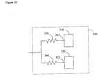
- FIG. 13schematically illustrates another exemplary memory module 500 compatible with certain embodiments described herein.
- the memory module 500comprises a termination bus 505 .
- the memory module 500further comprises a first memory device 510 having a first data strobe pin 512 , a first termination signal pin 514 electrically coupled to the termination bus 505 , a first termination circuit 516 , and at least one data pin 518 .
- the first termination circuit 516selectively electrically terminating the first data strobe pin 512 and the first data pin 518 in response to a first signal received by the first termination signal pin 514 from the termination bus 505 .
- the memory module 500further comprises a second memory device 520 having a second data strobe pin 522 electrically coupled to the first data strobe pin 512 , a second termination signal pin 524 , a second termination circuit 526 , and at least one data pin 528 .
- the second termination signal pin 524is electrically coupled to a voltage, wherein the second termination circuit 526 is responsive to the voltage by not terminating the second data strobe pin 522 or the second data pin 528 .
- the memory module 500further comprises at least one termination assembly 530 having a third termination signal pin 534 , a third termination circuit 536 , and at least one termination pin 538 electrically coupled to the data pin 528 of the second memory device 520 .
- the third termination signal pin 534is electrically coupled to the termination bus 505 .
- the third termination circuit 536selectively electrically terminates the data pin 528 of the second memory device 520 through the termination pin 538 in response to a second signal received by the third termination signal pin 534 from the termination bus 505 .
- FIG. 14schematically illustrates a particular embodiment of the memory module 500 schematically illustrated by FIG. 13 .
- the memory module 500comprises an on-die termination (ODT) bus 505 .
- the memory module 500comprises a first memory device 510 having a first data strobe (DQS) pin 512 , a first ODT signal pin 514 electrically coupled to the ODT bus 505 , a first ODT circuit 516 , and at least one data (DQ) pin 518 .
- the first ODT circuit 516selectively electrically terminates the first DQS pin 512 and the DQ pin 518 of the first memory device 510 in response to an ODT signal received by the first ODT signal pin 514 from the ODT bus 505 .
- This behavior of the first ODT circuit 516is schematically illustrated in FIG. 14 by the switches 572 , 576 which are selectively closed (dash-dot line) or opened (solid line).
- the memory module 500further comprises a second memory device 520 having a second DQS pin 522 electrically coupled to the first DQS pin 512 , a second ODT signal pin 524 , a second ODT circuit 526 , and at least one DQ pin 528 .
- the first DQS pin 512 and the second DQS pin 522are concurrently active when the first memory device 510 and the second memory device 520 are concurrently enabled.
- the second ODT signal pin 524is electrically coupled to a voltage (e.g., ground), wherein the second ODT circuit 526 is responsive to the voltage by not terminating the second DQS pin 522 or the second DQ pin 524 .
- This behavior of the second ODT circuit 526is schematically illustrated in FIG. 14 by the switches 574 , 578 which are opened.
- the memory module 500further comprises at least one termination assembly 530 having a third ODT signal pin 534 electrically coupled to the ODT bus 505 , a third ODT circuit 536 , and at least one termination pin 538 electrically coupled to the DQ pin 528 of the second memory device 520 .
- the third ODT circuit 536selectively electrically terminates the DQ pin 528 of the second memory device 520 through the termination pin 538 in response to an ODT signal received by the third ODT signal pin 534 from the ODT bus 505 .
- This behavior of the third ODT circuit 536is schematically illustrated in FIG. 14 by the switch 580 which is either closed (dash-dot line) or opened (solid line).
- the termination assembly 530comprises discrete electrical components which are surface-mounted or embedded on the printed-circuit board of the memory module 500 . In certain other embodiments, the termination assembly 530 comprises an integrated circuit mounted on the printed-circuit board of the memory module 500 . Persons skilled in the art can provide a termination assembly 530 in accordance with embodiments described herein.
- each of the first ODT circuit 516 , the second ODT circuit 526 , and the third ODT circuit 536are responsive to a high voltage or signal level by enabling the corresponding termination resistors and are responsive to a low voltage or signal level (e.g., ground) by disabling the corresponding termination resistors.
- each of the first ODT circuit 516 , the second ODT circuit 526 , and the third ODT circuit 536are responsive to a high voltage or signal level by disabling the corresponding termination resistors and are responsive to a low voltage or signal level (e.g., ground) by enabling the corresponding termination resistors.
- the switches 572 , 574 , 576 , 578 , 580 of FIG. 14are schematic representations of the enabling and disabling operation of the ODT circuits 516 , 526 , 536 and do not signify that the ODT circuits 516 , 526 , 536 necessarily include mechanical switches.
- the first ODT signal pin 514 of the first memory device 510receives an ODT signal from the ODT bus 505 .
- the first ODT circuit 516selectively enables or disables the termination resistance for both the first DQS pin 512 and the DQ pin 518 of the first memory device 510 .
- the second ODT signal pin 524 of the second memory device 520is tied (e.g., directly hard-wired) to the voltage (e.g., ground), thereby disabling the internal termination resistors 554 , 558 on the second DQS pin 522 and the second DQ pin 528 , respectively, of the second memory device 520 (schematically shown by open switches 574 , 578 in FIG. 14 ).
- the second DQS pin 522is electrically coupled to the first DQS pin 512 , so the termination resistance for both the first DQS pin 512 and the second DQS pin 522 is provided by the termination resistor 552 internal to the first memory device 510 .
- the termination resistor 556 of the DQ pin 518 of the first memory device 510is enabled or disabled by the ODT signal received by the first ODT signal pin 514 of the first memory device 510 from the ODT bus 505 .
- the termination resistance of the DQ pin 528 of the second memory device 520is enabled or disabled by the ODT signal received by the third ODT signal pin 534 of the termination assembly 530 which is external to the second memory device 520 .
- the first ODT signal pin 514 and the third ODT signal pin 534receive the same ODT signal from the ODT bus 505 , and the termination resistances for both the first memory device 510 and the second memory device 520 are selectively enabled or disabled in response thereto when these memory devices are concurrently enabled. In this way, certain embodiments of the memory module 500 schematically illustrated by FIG. 14 provides external or off-chip termination of the second memory device 520 .
- Certain embodiments of the memory module 500 schematically illustrated by FIG. 14advantageously allow the use of two lower-cost readily-available 512-Mb DDR-2 SDRAM devices to provide the capabilities of a more expensive 1-GB DDR-2 SDRAM device. Certain such embodiments advantageously reduce the total cost of the resultant memory module 500 .
- Certain embodiments described hereinadvantageously increase the memory capacity or memory density per memory slot or socket on the system board of the computer system. Certain embodiments advantageously allow for higher memory capacity in systems with limited memory slots. Certain embodiments advantageously allow for flexibility in system board design by allowing the memory module 10 to be used with computer systems designed for different numbers of ranks (e.g., either with computer systems designed for two-rank memory modules or with computer systems designed for four-rank memory modules). Certain embodiments advantageously provide lower costs of board designs.
- the memory density of a memory moduleis advantageously doubled by providing twice as many memory devices as would otherwise be provided.
- pairs of lower-density memory devicescan be substituted for individual higher-density memory devices to reduce costs or to increase performance.
- twice the number of memory devicescan be used to produce a higher-density memory configuration of the memory module.
- Each of these examplescan be limited by the number of chip select signals which are available from the memory controller or by the size of the memory devices.
Landscapes
- Engineering & Computer Science (AREA)
- Theoretical Computer Science (AREA)
- Physics & Mathematics (AREA)
- General Engineering & Computer Science (AREA)
- General Physics & Mathematics (AREA)
- Microelectronics & Electronic Packaging (AREA)
- Mathematical Physics (AREA)
- Dram (AREA)
Abstract
Description
- The present application is a continuation-in-part of U.S. patent application Ser. No. 11/075,395, filed Mar. 7, 2005, which claims the benefit of U.S. Provisional Application No. 60/550,668, filed Mar. 5, 2004 and U.S. Provisional Application No. 60/575,595, filed May 28, 2004. The present application also claims the benefit of U.S. Provisional Application No. 60/588,244, filed Jul. 15, 2004, which is incorporated in its entirety by reference herein.
- 1. Field of the Invention
- The present invention relates generally to memory modules of a computer system, and more specifically to devices and methods for improving the performance, the memory capacity, or both, of memory modules.
- 2. Description of the Related Art
- Certain types of memory modules comprise a plurality of dynamic random-access memory (DRAM) devices mounted on a printed circuit board (PCB). These memory modules are typically mounted in a memory slot or socket of a computer system (e.g., a server system or a personal computer) and are accessed by the processor of the computer system. Memory modules typically have a memory configuration with a unique combination of rows, columns, and banks which result in a total memory capacity for the memory module.
- For example, a 512-Megabyte memory module (termed a “512-MB” memory module, which actually has 229or 536,870,912 bytes of capacity) will typically utilize eight 512-Megabit DRAM devices (each identified as a “512-Mb” DRAM device, each actually having 229or 536,870,912 bits of capacity). The memory cells (or memory locations) of each 512-Mb DRAM device can be arranged in four banks, with each bank having an array of 224(or 16,777,216) memory locations arranged as 213rows and 211columns, and with each memory location having a width of 8 bits. Such DRAM devices with 64M 8-bit-wide memory locations (actually with four banks of 227or 134,217,728 one-bit memory cells arranged to provide a total of 226or 67,108,864 memory locations with 8 bits each) are identified as having a “64 Mb×8” or “64M×8-bit” configuration, or as having a depth of 64M and a bit width of 8. Furthermore, certain commercially-available 512-MB memory modules are termed to have a “64M×8-byte” configuration or a “64M×64-bit” configuration with a depth of 64M and a width of 8 bytes or 64 bits.
- Similarly, a 1-Gigabyte memory module (termed a “1-GB” memory module, which actually has 230or 1,073,741,824 bytes of capacity) can utilize eight 1-Gigabit DRAM devices (each identified as a “1-Gb” DRAM device, each actually having 230or 1,073,741,824 bits of capacity). The memory locations of each 1-Gb DRAM device can be arranged in four banks, with each bank having an array of memory locations with 214rows and 211columns, and with each memory location having a width of 8 bits. Such DRAM devices with 128M 8-bit-wide memory locations (actually with a total of 227or 134,217,728 memory locations with 8 bits each) are identified as having a “128 Mb×8” or “128M×8-bit” configuration, or as having a depth of 128M and a bit width of 8. Furthermore, certain commercially-available 1-GB memory modules are identified as having a “128M×8-byte” configuration or a “128M×64-bit” configuration with a depth of 128M and a width of 8 bytes or 64 bits.
- The commercially-available 512-MB (64M×8-byte) memory modules and the 1-GB (128M×8-byte) memory modules described above are typically used in computer systems (e.g., personal computers) which perform graphics applications since such “×8” configurations are compatible with data mask capabilities often used in such graphics applications. Conversely, memory modules with “×4” configurations are typically used in computer systems such as servers which are not as graphics-intensive. Examples of such commercially available “×4” memory modules include, but are not limited to, 512-MB (128M×4-byte) memory modules comprising eight 512-Mb (128 Mb×4) memory devices.
- The DRAM devices of a memory module are generally arranged as ranks or rows of memory, each rank of memory generally having a bit width. For example, a memory module in which each rank of the memory module is 64 bits wide is described as having an “×64” organization. Similarly, a memory module having 72-bit-wide ranks is described as having an “×72” organization.
- The memory capacity of a memory module increases with the number of memory devices. The number of memory devices of a memory module can be increased by increasing the number of memory devices per rank or by increasing the number of ranks. For example, a memory module with four ranks has double the memory capacity of a memory module with two ranks and four times the memory capacity of a memory module with one rank. Rather than referring to the memory capacity of the memory module, in certain circumstances, the memory density of the memory module is referred to instead.
- During operation, the ranks of a memory module are selected or activated by control signals that are received from the processor. Examples of such control signals include, but are not limited to, rank-select signals, also called chip-select signals. Most computer and server systems support one-rank and two-rank memory modules. By only supporting one-rank and two-rank memory modules, the memory density that can be incorporated in each memory slot is limited.
- In certain embodiments, a memory module is connectable to a computer system. The memory module comprises a printed circuit board, a plurality of memory devices coupled to the printed circuit board, and a logic element coupled to the printed circuit board. The plurality of memory devices has a first number of memory devices. The logic element receives a set of input control signals from the computer system. The set of input control signals corresponds to a second number of memory devices smaller than the first number of memory devices. The logic element generates a set of output control signals in response to the set of input control signals. The set of output control signals corresponds to the first number of memory devices.
- In certain embodiments, a method utilizes a memory module in a computer system. The method comprises coupling the memory module to the computer system. The memory module comprises a plurality of memory devices arranged in a first number of ranks. The method further comprises inputting a first set of control signals to the memory module. The first set of control signals corresponds to a second number of ranks smaller than the first number of ranks. The method further comprises generating a second set of control signals in response to the first set of control signals. The second set of control signals corresponds to the first number of ranks.
- In certain embodiments, a memory module is connectable to a computer system. The memory module comprises a plurality of memory devices arranged in a first number of ranks. The memory module comprises means for coupling the memory module to the computer system. The memory module further comprises means for inputting a first set of control signals to the memory module. The first set of control signals corresponds to a second number of ranks smaller than the first number of ranks. The memory module further comprises means for generating a second set of control signals in response to the first set of control signals. The second set of control signals corresponds to the first number of ranks.
- In certain embodiments, a memory module is connectable to a computer system. The memory module comprises a first memory device having a first data signal line and a first data strobe signal line. The memory module further comprises a second memory device having a second data signal line and a second data strobe signal line. The memory module further comprises a common data signal line connectable to the computer system. The memory module further comprises an isolation device electrically coupled to the first data signal line, to the second data signal line, and to the common data signal line. The isolation device selectively alternates between electrically coupling the first data signal line to the common data signal line and electrically coupling the second data signal line to the common data signal line.
FIG. 1A schematically illustrates an exemplary memory module with four ranks of memory devices compatible with certain embodiments described herein.FIG. 1B schematically illustrates an exemplary memory module with two ranks of memory devices compatible with certain embodiments described herein.FIG. 1C schematically illustrates another exemplary memory module in accordance with certain embodiments described herein.FIG. 2A schematically illustrates an exemplary memory module which doubles the rank density in accordance with certain embodiments described herein.FIG. 2B schematically illustrates an exemplary logic element compatible with embodiments described herein.FIG. 3A schematically illustrates an exemplary memory module which doubles number of ranks in accordance with certain embodiments described herein.FIG. 3B schematically illustrates an exemplary logic element compatible with embodiments described herein.FIG. 4A shows an exemplary timing diagram of a gapless read burst for a back-to-back adjacent read condition from one memory device.FIG. 4B shows an exemplary timing diagram with an extra clock cycle between successive read commands issued to different memory devices for successive read accesses from different memory devices.FIG. 5 shows an exemplary timing diagram in which the last data strobe of memory device “a” collides with the pre-amble time interval of the data strobe of memory device “b.”FIG. 6A schematically illustrates a circuit diagram of a conventional memory module showing the interconnections between the DQ data signal lines of two memory devices and their DQS data strobe signal lines.FIG. 6B schematically illustrates a circuit diagram of an exemplary memory module comprising an isolation device in accordance with certain embodiments described herein.FIG. 6C schematically illustrates an isolation device comprising a logic element which multiplexes the DQS data strobe signal lines from one another.FIG. 6D schematically illustrates an isolation device which multiplexes the DQS data strobe signal lines from one another and which multiplexes the DQ data signal lines from one another.FIG. 6E schematically illustrates an isolation device which comprises the logic element on the DQ data signal lines but not a corresponding logic element on the DQS data strobe signal lines.FIG. 7 schematically illustrates an exemplary memory module in which a data strobe (DQS) pin of a first memory device is electrically connected to a DQS pin of a second memory device while both DQS pins are active.FIG. 8 is an exemplary timing diagram of the voltages applied to the two DQS pins due to non-simultaneous switching.FIG. 9 schematically illustrates another exemplary memory module in which a DQS pin of a first memory device is connected to a DQS pin of a second memory device.FIG. 10 schematically illustrates an exemplary memory module in accordance with certain embodiments described herein.FIGS. 11A and 11B schematically illustrate a first side and a second side, respectively, of a memory module with eighteen 64M×4 bit, DDR-1 SDRAM FBGA memory devices on each side of a 184-pin glass-epoxy printed circuit board.FIGS. 12A and 12B schematically illustrate an exemplary embodiment of a memory module in which a first resistor and a second resistor are used to reduce the current flow between the first DQS pin and the second DQS pin.FIG. 13 schematically illustrates another exemplary memory module compatible with certain embodiments described herein.FIG. 14 schematically illustrates a particular embodiment of the memory module schematically illustrated byFIG. 13 .- Most high-density memory modules are currently built with 512-Megabit (“512-Mb”) memory devices wherein each memory device has a 64M×8-bit configuration. For example, a 1-Gigabyte (“1-GB”) memory module with error checking capabilities can be fabricated using eighteen such 512-Mb memory devices. Alternatively, it can be economically advantageous to fabricate a 1-GB memory module using lower-density memory devices and doubling the number of memory devices used to produce the desired word width. For example, by fabricating a 1-GB memory module using thirty-six 256-Mb memory devices with 64M×4-bit configuration, the cost of the resulting 1-GB memory module can be reduced since the unit cost of each 256-Mb memory device is typically lower than one-half the unit cost of each 512-Mb memory device. The cost savings can be significant, even though twice as many 256-Mb memory devices are used in place of the 512-Mb memory devices.
- Market pricing factors for DRAM devices are such that higher-density DRAM devices (e.g., 1-Gb DRAM devices) are much more than twice the price of lower-density DRAM devices (e.g., 512-Mb DRAM devices). In other words, the price per bit ratio of the higher-density DRAM devices is greater than that of the lower-density DRAM devices. This pricing difference often lasts for months or even years after the introduction of the higher-density DRAM devices, until volume production factors reduce the costs of the newer higher-density DRAM devices. Thus, when the cost of a higher-density DRAM device is more than the cost of two lower-density DRAM devices, there is an economic incentive for utilizing pairs of the lower-density DRAM devices to replace individual higher-density DRAM devices.
FIG. 1A schematically illustrates anexemplary memory module 10 compatible with certain embodiments described herein. Thememory module 10 is connectable to a computer system (not shown). Thememory module 10 comprises a printedcircuit board 20 and a plurality ofmemory devices 30 coupled to the printedcircuit board 20. The plurality ofmemory devices 30 has a first number of memory devices. Thememory module 10 further comprises alogic element 40 coupled to the printedcircuit board 20. Thelogic element 40 receives a set of input control signals from the computer system. The set of input control signals correspond to a second number of memory devices smaller than the first number of memory devices. Thelogic element 40 generates a set of output control signals in response to the set of input control signals. The set of output control signals corresponds to the first number of memory devices.- In certain embodiments, as schematically illustrated in
FIG. 1A , thememory module 10 further comprises a phase-lock loop device 50 coupled to the printedcircuit board 20 and aregister 60 coupled to the printedcircuit board 20. In certain embodiments, the phase-lock loop device 50 and theregister 60 are each mounted on the printedcircuit board 20. In response to signals received from the computer system, the phase-lock loop device 50 transmits clock signals to the plurality ofmemory devices 30, thelogic element 40, and theregister 60. Theregister 60 receives and buffers a plurality of control signals, including address signals (e.g., bank address signals, row address signals, column address signals, gated column address strobe signals, chip-select signals), and transmits corresponding signals to theappropriate memory devices 30. In certain embodiments, theregister 60 comprises a plurality of register devices. While the phase-lock loop device 50, theregister 60, and thelogic element 40 are described herein in certain embodiments as being separate components, in certain other embodiments, two or more of the phase-lock loop device 50, theregister 60, and thelogic element 40 are portions of a single component. Persons skilled in the art are able to select a phase-lock loop device 50 and aregister 60 compatible with embodiments described herein. - In certain embodiments, the
memory module 10 further comprises electrical components which are electrically coupled to one another and are surface-mounted or embedded on the printedcircuit board 20. These electrical components can include, but are not limited to, electrical conduits, resistors, capacitors, inductors, and transistors. In certain embodiments, at least some of these electrical components are discrete, while in other certain embodiments, at least some of these electrical components are constituents of one or more integrated circuits. - Various types of
memory modules 10 are compatible with embodiments described herein. For example,memory modules 10 having memory capacities of 512-MB, 1-GB, 2-GB, 4-GB, 8-GB, as well as other capacities, are compatible with embodiments described herein. In addition,memory modules 10 having widths of 4 bytes, 8 bytes, 16 bytes, 32 bytes, or 32 bits, 64 bits, 128 bits, 256 bits, as well as other widths (in bytes or in bits), are compatible with embodiments described herein. Furthermore,memory modules 10 compatible with embodiments described herein include, but are not limited to, single in-line memory modules (SIMMs), dual in-line memory modules (DIMMs), small-outline DIMMs (SO-DIMMs), unbuffered DIMMs (UDIMMs), registered DIMMs (RDIMMs), fully-buffered DIMM (FBDIMM), mini-DIMMs, and micro-DIMMs. - In certain embodiments, the printed
circuit board 20 is mountable in a module slot of the computer system. The printedcircuit board 20 of certain such embodiments has a plurality of edge connections electrically coupled to corresponding contacts of the module slot and to the various components of thememory module 10, thereby providing electrical connections between the computer system and the components of thememory module 10. Memory devices 30 compatible with embodiments described herein include, but are not limited to, random-access memory (RAM), dynamic random-access memory (DRAM), synchronous DRAM (SDRAM), and double-data-rate DRAM (e.g., DDR-1, DDR-2, DDR-3). In addition,memory devices 30 having bit widths of 4, 8, 16, 32, as well as other bit widths, are compatible with embodiments described herein.Memory devices 30 compatible with embodiments described herein have packaging which include, but are not limited to, thin small-outline package (TSOP), ball-grid-array (BGA), fine-pitch BGA (FBGA), micro-BGA (μBGA), mini-BGA (mBGA), and chip-scale packaging (CSP).Memory devices 30 compatible with embodiments described herein are available from a number of sources, including but not limited to, Samsung Semiconductor, Inc. of San Jose, Calif., Infineon Technologies AG of San Jose, Calif., and Micron Technology, Inc. of Boise, Id. Persons skilled in the art can selectappropriate memory devices 30 in accordance with certain embodiments described herein.- In certain embodiments, the plurality of
memory devices 30 are arranged in a first number of ranks. For example, in certain embodiments, thememory devices 30 are arranged in four ranks, as schematically illustrated byFIG. 1A . In other embodiments, thememory devices 30 are arranged in two ranks, as schematically illustrated byFIG. 1B . Other numbers of ranks of thememory devices 30 are also compatible with embodiments described herein. - In certain embodiments, the
logic element 40 comprises a programmable-logic device (PLD), an application-specific integrated circuit (ASIC), a field-programmable gate array (FPGA), a custom-designed semiconductor device, or a complex programmable-logic device (CPLD). In certain embodiments, thelogic element 40 is a custom device. Sources oflogic elements 40 compatible with embodiments described herein include, but are not limited to, Lattice Semiconductor Corporation of Hillsboro, Oreg., Altera Corporation of San Jose, Calif., and Xilinx Incorporated of San Jose, Calif. In certain embodiments, thelogic element 40 comprises various discrete electrical elements, while in certain other embodiments, thelogic element 40 comprises one or more integrated circuits. Persons skilled in the art can select anappropriate logic element 40 in accordance with certain embodiments described herein. - As schematically illustrated by
FIGS. 1A and 1B , in certain embodiments, thelogic element 40 receives a set of input control signals, which includes address signals (e.g., bank address signals, row address signals, column address signals, gated column address strobe signals, chip-select signals) and command signals (e.g., refresh, precharge) from the computer system. In response to the set of input control signals, thelogic element 40 generates a set of output control signals which includes address signals and command signals. - In certain embodiments, the set of output control signals corresponds to a first number of ranks in which the plurality of
memory devices 30 of thememory module 10 are arranged, and the set of input control signals corresponds to a second number of ranks per memory module for which the computer system is configured. The second number of ranks in certain embodiments is smaller than the first number of ranks. For example, in the exemplary embodiment as schematically illustrated byFIG. 1A , the first number of ranks is four while the second number of ranks is two. In the exemplary embodiment ofFIG. 1B , the first number of ranks is two while the second number of ranks is one. Thus, in certain embodiments, even though thememory module 10 actually has the first number of ranks ofmemory devices 30, thememory module 10 simulates a virtual memory module by operating as having the second number of ranks ofmemory devices 30. In certain embodiments, thememory module 10 simulates a virtual memory module when the number ofmemory devices 30 of thememory module 10 is larger than the number ofmemory devices 30 per memory module for which the computer system is configured to utilize. - In certain embodiments, the computer system is configured for a number of ranks per memory module which is smaller than the number of ranks in which the
memory devices 30 of thememory module 10 are arranged. In certain such embodiments, the computer system is configured for two ranks of memory per memory module (providing two chip-select signals CS0, CS1) and the plurality ofmemory modules 30 of thememory module 10 are arranged in four ranks, as schematically illustrated byFIG. 1A . In certain other such embodiments, the computer system is configured for one rank of memory per memory module (providing one chip-select signal CS0) and the plurality ofmemory modules 30 of thememory module 10 are arranged in two ranks, as schematically illustrated byFIG. 1B . - In the exemplary embodiment schematically illustrated by
FIG. 1A , thememory module 10 has four ranks ofmemory devices 30 and the computer system is configured for two ranks of memory devices per memory module. Thememory module 10 receives row/column address signals or signal bits (A0-An+1), bank address signals (BA0-BAm), chip-select signals (CS0and CS1), and command signals (e.g., refresh, precharge, etc.) from the computer system. The A0-Anrow/column address signals are received by theregister 60, which buffers these address signals and sends these address signals to the appropriate ranks ofmemory devices 30. Thelogic element 40 receives the two chip-select signals (CS0, CS1) and one row/column address signal (An+1) from the computer system. Both thelogic element 40 and theregister 60 receive the bank address signals (BA0-BAm) and at least one command signal (e.g., refresh, precharge, etc.) from the computer system. - Logic Tables
- Table 1 provides a logic table compatible with certain embodiments described herein for the selection among ranks of
memory devices 30 using chip-select signals.TABLE 1 State CS0 CS1 An+1 Command CS0A CS0B CS1A CS1B 1 0 1 0 Active 0 1 1 1 2 0 1 1 Active 1 0 1 1 3 0 1 x Active 0 0 1 1 4 1 0 0 Active 1 1 0 1 5 1 0 1 Active 1 1 1 0 6 1 0 x Active 1 1 0 0 7 1 1 x x 1 1 1 1
Note:
1. Cs0, CS1, CS0A, CS0B, CS1A, and CS1Bare active low signals.
2. An+1is an active high signal.
3. ‘x’ is a Don't Care condition.
4. Command involves a number of command signals that define operations such as refresh, precharge, and other operations. - In Logic State 1: CS0is active low, An+1is non-active, and Command is active. CS0Ais pulled low, thereby selecting
Rank 0. - In Logic State 2: CS0is active low, An+1is active, and Command is active. CS0Bis pulled low, thereby selecting
Rank 1. - In Logic State 3: CS0is active low, An+1is Don't Care, and Command is active high. CS0Aand CS0Bare pulled low, thereby selecting
Ranks - In Logic State 4: CS1is active low, An+1is non-active, and Command is active. CS1Ais pulled low, thereby selecting Rank 2.
- In Logic State 5: CS1is active low, An+1is active, and Command is active. CS1Bis pulled low, thereby selecting Rank 3.
- In Logic State 6: CS1is active low, An+1is Don't Care, and Command is active. CS1Aand CS1Bare pulled low, thereby selecting Ranks 2 and 3.
- In Logic State 7: CS0and CS1are pulled non-active high, which deselects all ranks, i.e., CS0A, CS0B, CS1A, and CS1Bare pulled high.
- The “Command” column of Table 1 represents the various commands that a memory device (e.g., a DRAM device) can execute, examples of which include, but are not limited to, activation, read, write, precharge, and refresh. In certain embodiments, the command signal is passed through to the selected rank only (e.g.,
state 4 of Table 1). In such embodiments, the command signal (e.g., read) is sent to only one memory device or the other memory device so that data is supplied from one memory device at a time. In other embodiments, the command signal is passed through to both associated ranks (e.g., state 6 of Table 1). In such embodiments, the command signal (e.g., refresh) is sent to both memory devices to ensure that the memory content of the memory devices remains valid over time. Certain embodiments utilize a logic table such as that of Table 1 to simulate a single memory device from two memory devices by selecting two ranks concurrently. - Table 2 provides a logic table compatible with certain embodiments described herein for the selection among ranks of
memory devices 30 using gated CAS signals.TABLE 2 CS* RAS* CAS* WE* Density Bit A10 Command CAS0* CAS1* 1 x x x x x NOP x x 0 1 1 1 x x NOP 1 1 0 0 1 1 0 x ACTIVATE 1 1 0 0 1 1 1 x ACTIVATE 1 1 0 1 0 1 0 x READ 0 1 0 1 0 1 1 x READ 1 0 0 1 0 0 0 x WRITE 0 1 0 1 0 0 1 x WRITE 1 0 0 0 1 0 0 0 PRECHARGE 1 1 0 0 1 0 1 0 PRECHARGE 1 1 0 0 1 0 x 1 PRECHARGE 1 1 0 0 0 0 x x MODE REG SET 0 0 0 0 0 1 x x REFRESH 0 0 - In certain embodiments in which the density bit is a row address bit, for read/write commands, the density bit is the value latched during the activate command for the selected bank.
- Serial-Presence-Detect Device
- Memory modules typically include a serial-presence detect (SPD) device70 (e.g., an electrically-erasable-programmable read-only memory or EEPROM device) comprising data which characterize various attributes of the memory module, including but not limited to, the number of row addresses the number of column addresses, the data width of the memory devices, the number of ranks, the memory density per rank, the number of memory devices, and the memory density per memory device. The
SPD device 70 communicates this data to the basic input/output system (BIOS) of the computer system so that the computer system is informed of the memory capacity and the memory configuration available for use and can configure the memory controller properly for maximum reliability and performance. - For example, for a commercially-available 512-MB (64M×8-byte) memory module utilizing eight 512-Mb memory devices each with a 64M×8-bit configuration, the SPD device contains the following SPD data (in appropriate bit fields of these bytes):
- Byte3: Defines the number of row address bits in the DRAM device in the memory module [13 for the 512-Mb memory device].
- Byte4: Defines the number of column address bits in the DRAM device in the memory module [11 for the 512-Mb memory device].
- Byte13: Defines the bit width of the primary DRAM device used in the memory module [8 bits for the 512-Mb (64M×8-bit) memory device].
- Byte14: Defines the bit width of the error checking DRAM device used in the memory module [8 bits for the 512-Mb (64M×8-bit) memory device].
- Byte17: Defines the number of banks internal to the DRAM device used in the memory module [4 for the 512-Mb memory device].
- In a further example, for a commercially-available 1-GB (128M×8-byte) memory module utilizing eight 1-Gb memory devices each with a 128M×8-bit configuration, as described above, the SPD device contains the following SPD data (in appropriate bit fields of these bytes):
- Byte3: Defines the number of row address bits in the DRAM device in the memory module [14 for the 1-Gb memory device].
- Byte4: Defines the number of column address bits in the DRAM device in the memory module [11 for the 1-Gb memory device].
- Byte13: Defines the bit width of the primary DRAM device used in the memory module [8 bits for the 1-Gb (128M×8-bit) memory device].
- Byte14: Defines the bit width of the error checking DRAM device used in the memory module [8 bits for the 1-Gb (128M×8-bit) memory device].
- Byte17: Defines the number of banks internal to the DRAM device used in the memory module [4 for the 1-Gb memory device].
- In certain embodiments, the
SPD device 70 comprises data which characterize thememory module 10 as having fewer ranks of memory devices than thememory module 10 actually has, with each of these ranks having more memory density. For example, for amemory module 10 compatible with certain embodiments described herein having two ranks ofmemory devices 30, theSPD device 70 comprises data which characterizes thememory module 10 as having one rank of memory devices with twice the memory density per rank. Similarly, for amemory module 10 compatible with certain embodiments described herein having four ranks ofmemory devices 30, theSPD device 70 comprises data which characterizes thememory module 10 as having two ranks of memory devices with twice the memory density per rank. In addition, in certain embodiments, theSPD device 70 comprises data which characterize thememory module 10 as having fewer memory devices than thememory module 10 actually has, with each of these memory devices having more memory density per memory device. For example, for amemory module 10 compatible with certain embodiments described herein, theSPD device 70 comprises data which characterizes thememory module 10 as having one-half the number of memory devices that thememory module 10 actually has, with each of these memory devices having twice the memory density per memory device. FIG. 1C schematically illustrates anexemplary memory module 10 in accordance with certain embodiments described herein. Thememory module 10 comprises a pair of substantiallyidentical memory devices memory device memory module 10 further comprises anSPD device 70 comprising data that characterizes the pair ofmemory devices memory devices - In certain such embodiments, the
SPD device 70 of thememory module 10 is programmed to describe the combined pair of lower-density memory devices SPD device 70 of thememory module 10 is programmed to describe the pair of 512-Mb memory devices as one virtual or pseudo-1-Gb memory device. - For example, to fabricate a 1-GB (128M×8-byte) memory module, sixteen 512-Mb (128M×4-bit) memory devices can be used. The sixteen 512-Mb (128M×4-bit) memory devices are combined in eight pairs, with each pair serving as a virtual or pseudo-1-Gb (128M×8-bit) memory device. In certain such embodiments, the
SPD device 70 contains the following SPD data (in appropriate bit fields of these bytes): - Byte3: 13 row address bits.
- Byte4: 12 column address bits.
- Byte13: 8 bits wide for the primary virtual 1-Gb (128M×8-bit) memory device.
- Byte14: 8 bits wide for the error checking virtual 1-Gb (128M×8-bit) memory device.
- Byte17: 4 banks.
- In this exemplary embodiment,
bytes 3,4, and17 are programmed to have the same values as they would have for a 512-MB (128M×4-byte) memory module utilizing 512-Mb (128M×4-bit) memory devices. However,bytes 13 and14 of the SPD data are programmed to be equal to 8, corresponding to the bit width of the virtual or pseudo-higher-density 1-Gb (128M×8-bit) memory device, for a total capacity of 1-GB. Thus, the SPD data does not describe the actual-lower-density memory devices, but instead describes the virtual or pseudo-higher-density memory devices. The BIOS accesses the SPD data and recognizes the memory module as having 4 banks of memory locations arranged in 213rows and 212columns, with each memory location having a width of 8 bits rather than 4 bits. - In certain embodiments, when such a
memory module 10 is inserted in a computer system, the computer system's memory controller then provides to the memory module10 a set of input control signals which correspond to the number of ranks or the number of memory devices reported by theSPD device 70. For example, placing a two-rank memory module 10 compatible with certain embodiments described herein in a computer system compatible with one-rank memory modules, theSPD device 70 reports to the computer system that thememory module 10 only has one rank. Thelogic element 40 then receives a set of input control signals corresponding to a single rank from the computer system's memory controller, and generates and transmits a set of output control signals corresponding to two ranks to theappropriate memory devices 30 of thememory module 10. Similarly, when a two-rank memory module 10 compatible with certain embodiments described herein is placed in a computer system compatible with either one- or two-rank memory modules, theSPD device 70 reports to the computer system that thememory module 10 only has one rank. Thelogic element 40 then receives a set of input control signals corresponding to a single rank from the computer system's memory controller, and generates and transmits a set of output control signals corresponding to two ranks to theappropriate memory devices 30 of thememory module 10. Furthermore, a four-rank memory module 10 compatible with certain embodiments described herein simulates a two-rank memory module whether thememory module 10 is inserted in a computer system compatible with two-rank memory modules or with two- or four-rank memory modules. Thus, by placing a four-rank memory module 10 compatible with certain embodiments described herein in a module slot that is four-rank-ready, the computer system provides four chip-select signals, but thememory module 10 only uses two of the chip-select signals. - Memory Density Multiplication
- In certain embodiments, two memory devices having a memory density are used to simulate a single memory device having twice the memory density, and an additional address signal bit is used to access the additional memory. Similarly, in certain embodiments, two ranks of memory devices having a memory density are used to simulate a single rank of memory devices having twice the memory density, and an additional address signal bit is used to access the additional memory. As used herein, such simulations of memory devices or ranks of memory devices are termed as “memory density multiplication,” and the term “density transition bit” is used to refer to the additional address signal bit which is used to access the additional memory.
- In certain embodiments utilizing memory density multiplication embodiments, the
memory module 10 can have various types of memory devices30 (e.g., DDR1, DDR2, DDR3, and beyond). Thelogic element 40 of certain such embodiments utilizes implied translation logic equations having variations depending on whether the density transition bit is a row, column, or internal bank address bit. In addition, the translation logic equations of certain embodiments vary depending on the type of memory module10 (e.g., UDIMM, RDIMM, FBDIMM, etc.). Furthermore, in certain embodiments, the translation logic equations vary depending on whether the implementation multiplies memory devices per rank or multiplies the number of ranks per memory module. - Table 3A provides the numbers of rows and columns for DDR-1 memory devices, as specified by JEDEC standard JESD79D, “Double Data Rate (DDR) SDRAM Specification,” published February 2004, and incorporated in its entirety by reference herein.
TABLE 3A 128-Mb 256-Mb 512-Mb 1-Gb Number of banks 4 4 4 4 Number of row address bits 12 13 13 14 Number of column address bits for 11 11 12 12 “×4” configuration Number of column address bits for 10 10 11 11 “×8” configuration Number of column address bits for 9 9 10 10 “×16” configuration - As described by Table 3A, 512-Mb (128M×4-bit) DRAM devices have 213rows and 212columns of memory locations, while 1-Gb (128M×8-bit) DRAM devices have 214rows and 211columns of memory locations. Because of the differences in the number of rows and the number of columns for the two types of memory devices, complex address translation procedures and structures would typically be needed to fabricate a 1-GB (128M×8-byte) memory module using sixteen 512-Mb (128M×4-bit) DRAM devices.
- Table 3B shows the device configurations as a function of memory density for DDR2 memory devices.
TABLE 3B Number of Number of Number of Page Size Rows Columns Internal Banks (×4s or ×8s) 256 Mb 13 10 4 1 KB 512 Mb 14 10 4 1 KB 1 Gb 14 10 8 1 KB 2 Gb 15 10 8 1 KB 4 Gb to be to be 8 1 KB determined determined - Table 4 lists the corresponding density transition bit for the density transitions between the DDR2 memory densities of Table 3B.
TABLE 4 Density Transition Density Transition Bit 256 Mb to 512 Mb A 13 512 Mb to 1 Gb BA 2 1 Gb to 2 Gb A14 2 Gb to 4 Gb to be determined
Because the standard memory configuration of 4-Gb DDR2 SDRAM modules is not yet determined by the appropriate standards-setting organization, Tables 3B and 4 have “to be determined” in the appropriate table entries. - In certain embodiments, the logic translation equations are programmed in the
logic element 40 by hardware, while in certain other embodiments, the logic translation equations are programmed in thelogic element 40 by software. Examples 1 and 2 provide exemplary sections of Verilog code compatible with certain embodiments described herein. As described more fully below, the code of Examples 1 and 2 includes logic to reduce potential problems due to “back-to-back adjacent read commands which cross memory device boundaries or “BBARX.” Persons skilled in the art are able to provide additional logic translation equations compatible with embodiments described herein. - An exemplary section of Verilog code compatible with memory density multiplication from 512 Mb to 1 Gb using DDR2 memory devices with the BA2density transition bit is listed below in Example 1. The exemplary code of Example 1 corresponds to a
logic element 40 which receives one chip-select signal from the computer system and which generates two chip-select signals. always @(posedge clk_in) begin rs0N_R <= rs0_in_N; // cs0 rasN_R <= ras_in_N; casN_R <= cas_in_N; weN_R <= we_in_N; end // Gated Chip Selects assign pcs0a_1 = (˜rs0_in_N & ˜ras_in_N & ˜cas_in_N) // ref,md reg set | (˜rs0_in_N & ras_in_N & cas_in_N) // ref exit, pwr dn | (˜rs0_in_N & ˜ras_in_N & cas_in_N & ˜we_in_N & a10_in) // pchg all | (˜rs0_in_N & ˜ras_in_N & cas_in_N & ˜we_in_N & ˜a10_in & ˜ba2_in)// pchg single bnk | (˜rs0_in_N & ˜ras_in_N & cas_in_N & we_in_N & ˜ba2_in) // activate | (˜rs0_in_N & ras_in_N & ˜cas_in_N & ˜ba2_in) // xfr ; assign pcs0b_1 = (˜rs0_in_N & ˜ras_in_N & ˜cas_in_N) // ref,md reg set | (˜rs0_in_N & ras_in_N & cas_in_N) // ref exit, pwr dn | (˜rs0_in_N & ˜ras_in_N & cas_in_N & ˜we_in_N & a10_in) // pchg all | (˜rs0_in_N & ˜ras_in_N & cas_in_N & ˜we_in_N & ˜a10_in & ba2_in)// pchg single bnk | (˜rs0_in_N & ˜ras_in_N & cas_in_N & we_in_N & ba2_in) // activate | (˜rs0_in_N & ras_in_N & ˜cas_in_N & ba2_in) // xfr ; //------------------------------------- always @(posedge_clk_in) begin a4_r <= a4_in ; a5_r <= a5_in ; a6_r <= a6_in ; a10_r <= a10_in ; ba0_r <= ba0_in ; ba1_r <= ba1_in ; ba2_r <= ba2_in ; q_mrs_cmd_cyc1 <= q_mrs_cmd ; end //////////////////////////////////////////////////////////////////////// // determine the cas latency //////////////////////////////////////////////////////////////////////// assign q_mrs_cmd_r = (!rasN_R & !casN_R & !weN_R) & !rs0N_R & (!ba0_r & !ba1_r) ; // md reg set cmd always @(posedge clk_in) if (˜reset_N) // lmr cl3 <= l ′b1 ; else if (q_mrs_cmd_cyc1) // load mode reg cmd begin cl3 <= (˜a6_r & a5_r & a4_r ) ; end always @(posedge clk_in) if (˜reset_N) // reset cl2 <= l ′b0 ; else if (q_mrs_cmd_cyc1) // load mode reg cmd begin cl2 <= (˜a6_r & a5_r & ˜a4_r ) ; end always @(posedge clk_in) if (˜reset_N) // reset cl4 <= l ′b0 ; else if (q_mrs_cmd_cyc1) // load mode reg cmd begin cl4 <= (a6_r & ˜a5_r & ˜a4_r ) ; end always @(posedge clk_in) if (˜reset_N) cl5 <= l ′b0 ; else if (q_mrs_cmd_cyc1) // load mode reg cmd begin cl5 <= (a6_r & ˜a5_r & a4_r ) ; end assign pre_cyc2_enfet = (wr_cmd_cyc1 & acs_cyc1 & cl3) // wr brst cl3 preamble ; assign pre_cyc3_enfet = (rd_cmd_cyc2 & cl3) // rd brst cl3 preamble | (wr_cmd_cyc2 & cl3) // wr brst cl3 1st pair | (wr_cmd_cyc2 & cl4) // wr brst cl4 preamble ; assign pre_cyc4_enfet = (wr_cmd_cyc3 & cl3) // wr brst cl3 2nd pair | (wr_cmd_cyc3 & cl4) // wr brst cl4 1st pair | (rd_cmd_cyc3 & cl3) // rd brst cl3 1st pair | (rd_cmd_cyc3 & cl4) // rd brst cl4 preamble ; assign pre_cyc5_enfet = (rd_cmd_cyc4 & cl3) // rd brst cl3 2nd pair | (wr_cmd_cyc4 & cl4) // wr brst cl4 2nd pair | (rd_cmd_cyc4 & cl4) // rd brst cl4 1st pair ; // dq assign pre_dq_cyc = pre_cyc2_enfet | pre_cyc3_enfet | pre_cyc4_enfet | pre_cyc5_enfet ; assign pre_dq_ncyc = enfet_cyc2 | enfet_cyc3 | enfet_cyc4 | enfet_cyc5 ; // dqs assign pre_dqsa_cyc = (pre_cyc2_enfet & ˜ba2_r) | (pre_cyc3_enfet & ˜ba2_cyc2) | (pre_cyc4_enfet & ˜ba2_cyc3) | (pre_cyc5_enfet & ˜ba2_cyc4) ; assign pre_dqsb_cyc = (pre_cyc2_enfet & ba2_r) | (pre_cyc3_enfet & ba2_cyc2) | (pre_cyc4_enfet & ba2_cyc3) | (pre_cyc5_enfet & ba2_cyc4) ; assign pre_dqsa_ncyc = (enfet_cyc2 & ˜ba2_cyc2) | (enfet_cyc3 & ˜ba2_cyc3) | (enfet_cyc4 & ˜ba2_cyc4) | (enfet_cyc5 & ˜ba2_cyc5) ; assign pre_dqsb_ncyc = (enfet_cyc2 & ba2_cyc2) | (enfet_cyc3 & ba2_cyc3) | (enfet_cyc4 & ba2_cyc4) | (enfet_cyc5 & ba2_cyc5) ; always @(posedge clk_in) begin acs_cyc2 <= acs_cyc1 ; // cs active ba2_cyc2 <= ba2_r ; ba2_cyc3 <= ba2_cyc2 ; ba2_cyc4 <= ba2_cyc3 ; ba2_cyc5 <= ba2_cyc4 ; rd_cmd_cyc2 <= rd_cmd_cyc1 & acs_cyc1; rd_cmd_cyc3 <= rd_cmd_cyc2 ; rd_cmd_cyc4 <= rd_cmd_cyc3 ; rd_cmd_cyc5 <= rd_cmd_cyc4 ; rd_cmd_cyc6 <= rd_cmd_cyc5 ; rd_cmd_cyc7 <= rd_cmd_cyc6 ; wr_cmd_cyc2 <= wr_cmd_cyc1 & acs_cyc1; wr_cmd_cyc3 <= wr_cmd_cyc2 ; wr_cmd_cyc4 <= wr_cmd_cyc3 ; wr_cmd_cyc5 <= wr_cmd_cyc4 ; end always @(negedge clk_in) begin dq_ncyc <= dq_cyc; dqs_ncyc_a <= dqs_cyc_a; dqs_ncyc_b <= dqs_cyc_b; end // DQ FET enables assign enq_fet1 = dq_cyc | dq_ncyc ; assign enq_fet2 = dq_cyc | dq_ncyc ; assign enq_fet3 = dq_cyc | dq_ncyc ; assign enq_fet4 = dq_cyc | dq_ncyc ; assign enq_fet5 = dq_cyc | dq_ncyc ; // DQS FET enables assign ens_fet1a = dqs_cyc_a | dqs_ncyc_a ; assign ens_fet2a = dqs_cyc_a | dqs_ncyc_a ; assign ens_fet3a = dqs_cyc_a | dqs_ncyc_a ; assign ens_fet1b = dqs_cyc_b | dqs_ncyc_b ; assign ens_fet2b = dqs_cyc_b | dqs_ncyc_b ; assign ens_fet3b = dqs_cyc_b | dqs_ncyc_b ; - Another exemplary section of Verilog code compatible with memory density multiplication from 256 Mb to 512 Mb using DDR2 memory devices and gated CAS signals with the row A13density transition bit is listed below in Example 2. The exemplary code of Example 2 corresponds to a
logic element 40 which receives one gated CAS signal from the computer system and which generates two gated CAS signals. // latched a13 flags cs0, banks 0-3 always @(posedge clk_in) if (actv_cmd_R & ˜rs0N_R & ˜bnk1_R & ˜bnk0_R) // activate begin l_a13_00 <= a13_r ; end always @(posedge clk_in) if (actv_cmd_R & ˜rs0N_R & ˜bnk1_R & bnk0_R) // activate begin l_a13_01 <= a13_r ; end always @(posedge clk_in) if (actv_cmd_R & ˜rs0N_R & bnk1_R & ˜bnk0_R) // activate begin l_a13_10 <= a13_r ; end always @(posedge clk_in) if (actv_cmd_R & ˜rs0N_R & bnk1_R & bnk0_R) // activate begin l_a13_11 <= a13_r ; end // gated cas assign cas_i = ˜(casN_R); assign cas0_o = ( ˜rasN_R & cas_i) | ( rasN_R & ˜l_a13_00 & ˜bnk1_R & ˜bnk0_R & cas_i) | ( rasN_R & ˜l_a13_01 & ˜bnk1_R & bnk0_R & cas_i) | ( rasN_R & ˜l_a13_10 & bnk1_R & ˜bnk0_R & cas_i) | ( rasN_R & ˜l_a13_11 & bnk1_R & bnk0_R & cas_i) ; assign cas1_o = ( ˜rasN_R & cas_i) | ( rasN_R & l_a13_00 & ˜bnk1_R & ˜bnk0_R & cas_i) | ( rasN_R & l_a13_01 & ˜bnk1_R & bnk0_R & cas_i) | ( rasN_R & l_a13_10 & bnk1_R & ˜bnk0_R & cas_i) | (rasN_R & l_a13_11 & bnk1_R & bnk0_R & cas_i) ; assign pcas_0_N = ˜cas0_o; assign pcas_1_N = ˜cas1_o; assign rd0_o_R1 = rasN_R & cas0_o & weN_R & ˜rs0N_R; // rnk0 rd cmd cyc assign rd1_o_R1 = rasN_R & cas1_o & weN_R & ˜rs0N_R; // rnk1 rd cmd cyc assign wr0_o_R1 = rasN_R & cas0_o & ˜weN_R & ˜rs0N_R; // rnk0 wr cmd cyc assign wr1_o_R1 = rasN_R & cas1_o & ˜weN_R & ˜rs0N_R ; // rnk1 wr cmd cyc always @(posedge clk_in) begin rd0_o_R2 <= rd0_o_R1 ; rd0_o_R3 <= rd0_o_R2; rd0_o_R4 <= rd0_o_R3; rd0_o_R5 <= rd0_o_R4; rd1_o_R2 <= rd1_o_R1 ; rd1_o_R3 <= rd1_o_R2; rd1_o_R4 <= rd1_o_R3; rd1_o_R5 <= rd1_o_R4; wr0_o_R2 <= wr0_o_R1 ; wr0_o_R3 <= wr0_o_R2; wr0_o_R4 <= wr0_o_R3; wr1_o_R2 <= wr1_o_R1 ; wr1_o_R3 <= wr1_o_R2; wr1_o_R4 <= wr1_o_R3; end always @(posedge clk_in) begin if ( (rd0_o_R2 & ˜rd1_o_R4) // pre-am rd if no ped on rnk 1 | rd0_o_R3 // 1st cyc of rd brst | rd0_o_R4 // 2nd cyc of rd brst | (rd0_o_R5 & ˜rd1_o_R2 & ˜rd1_o_R3) // post-rd cyc if no ped on rnk 1 | (wr0_o_R1) // pre-am wr | wr0_o_R2 | wr0_o_R3 // wr brst 1st & 2nd cyc | (wr0_o_R4) // post-wr cyc (chgef9) | wr1_o_R1 | wr1_o_R2 | wr1_o_R3 | wr1_o_R4 // rank 1 (chgef9) ) en_fet_a <= l ′b1; // enable fet else en_fet_a <= l ′b0; // disable fet end always @(posedge clk_in) begin if ( (rd1_o_R2 & ˜rd0_o_R4) | rd1_o_R3 | rd1_o_R4 | (rd1_o_R5 & ˜rd0_o_R2 & ˜rd0_o_R3) | (wr1_o_R1) // (chgef8) | wr1_o_R2 | wr1_o_R3 | (wr1_o_R4) // post-wr cyc (chgef9) | wr0_o_R1 | wr0_o_R2 | wr0_o_R3 | wr0_o_R4 // rank 0 (chgef9) ) en_fet_b <= l ′b1; // else en_fet_b <= l ′b0; end FIG. 2A schematically illustrates anexemplary memory module 10 which doubles the rank density in accordance with certain embodiments described herein. Thememory module 10 has a first memory capacity. Thememory module 10 comprises a plurality of substantiallyidentical memory devices 30 configured as afirst rank 32 and asecond rank 34. In certain embodiments, thememory devices 30 of thefirst rank 32 are configured in pairs, and thememory devices 30 of thesecond rank 34 are also configured in pairs. In certain embodiments, thememory devices 30 of thefirst rank 32 are configured with their respective DQS pins tied together and thememory devices 30 of thesecond rank 34 are configured with their respective DQS pins tied together, as described more fully below. Thememory module 10 further comprises alogic element 40 which receives a first set of address and control signals from a memory controller (not shown) of the computer system. The first set of address and control signals is compatible with a second memory capacity substantially equal to one-half of the first memory capacity. Thelogic element 40 translates the first set of address and control signals into a second set of address and control signals which is compatible with the first memory capacity of thememory module 10 and which is transmitted to thefirst rank 32 and thesecond rank 34.- The
first rank 32 ofFIG. 2A has 18memory devices 30 and thesecond rank 34 ofFIG. 2A has 18memory devices 30. Other numbers ofmemory devices 30 in each of theranks - In the embodiment schematically illustrated by
FIG. 2A , thememory module 10 has a width of 8 bytes (or 64 bits) and each of thememory devices 30 ofFIG. 2A has a bit width of 4 bits. The 4-bit-wide (“×4”)memory devices 30 ofFIG. 2A have one-half the width, but twice the depth of 8-bit-wide (“×8”) memory devices. Thus, each pair of “×4”memory devices 30 has the same density as a single “×8” memory device, and pairs of “×4”memory devices 30 can be used instead of individual “×8” memory devices to provide the memory density of thememory module 10. For example, a pair of 512-Mb 128M×4-bit memory devices has the same memory density as a 1-Gb 128M×8-bit memory device. - For two “×4”
memory devices 30 to work in tandem to mimic a “×8” memory device, the relative DQS pins of the twomemory devices 30 in certain embodiments are advantageously tied together, as described more fully below. In addition, to access the memory density of a high-density memory module 10 comprising pairs of “×4”memory devices 30, an additional address line is used. While a high-density memory module comprising individual “×8” memory devices with the next-higher density would also utilize an additional address line, the additional address lines are different in the two memory module configurations. - For example, a 1-Gb 128M×8-bit DDR-1 DRAM memory device uses row addresses A13-A0and column addresses A11and A0-A0. A pair of 512-Mb 128M×4-bit DDR-1 DRAM memory devices uses row addresses A12-A0and column addresses A12, A11, and A9-A0. In certain embodiments, a memory controller of a computer system utilizing a 1-GB 128M×8
memory module 10 comprising pairs of the 512-Mb 128M×4memory devices 30 supplies the address and control signals including the extra row address (A13) to thememory module 10. Thelogic element 40 receives the address and control signals from the memory controller and converts the extra row address (A13) into an extra column address (A12). FIG. 2B schematically illustrates anexemplary logic element 40 compatible with embodiments described herein. Thelogic element 40 is used for amemory module 10 comprising pairs of “×4”memory devices 30 which mimic individual “×8” memory devices. In certain embodiments, each pair has the respective DQS pins of thememory devices 30 tied together. In certain embodiments, as schematically illustrated byFIG. 2B , thelogic element 40 comprises a programmable-logic device (PLD)42, afirst multiplexer 44 electrically coupled to thefirst rank 32 ofmemory devices 30, and asecond multiplexer 46 electrically coupled to thesecond rank 34 ofmemory devices 30. In certain embodiments, thePLD 42 and the first andsecond multiplexers appropriate PLD 42,first multiplexer 44, andsecond multiplexer 46 in accordance with embodiments described herein.- In the
exemplary logic element 40 ofFIG. 2B , during a row access procedure (CAS is high), thefirst multiplexer 44 passes the A12address through to thefirst rank 32, thesecond multiplexer 46 passes the A12address through to thesecond rank 34, and thePLD 42 saves or latches the A13address from the memory controller. In certain embodiments, a copy of the A13address is saved by thePLD 42 for each of the internal banks (e.g., 4 internal banks) permemory device 30. During a subsequent column access procedure (CAS is low), thefirst multiplexer 44 passes the previously-saved A13address through to thefirst rank 32 as the A12address and thesecond multiplexer 46 passes the previously-saved A13address through to thesecond rank 34 as the A12address. Thefirst rank 32 and thesecond rank 34 thus interpret the previously-saved A13row address as the current A12column address. In this way, in certain embodiments, thelogic element 40 translates the extra row address into an extra column address in accordance with certain embodiments described herein. - Thus, by allowing two lower-density memory devices to be used rather than one higher-density memory device, certain embodiments described herein provide the advantage of using lower-cost, lower-density memory devices to build “next-generation” higher-density memory modules. Certain embodiments advantageously allow the use of lower-cost readily-available 512-Mb DDR-2 SDRAM devices to replace more expensive 1-Gb DDR-2 SDRAM devices. Certain embodiments advantageously reduce the total cost of the resultant memory module.
FIG. 3A schematically illustrates anexemplary memory module 10 which doubles number of ranks in accordance with certain embodiments described herein. Thememory module 10 has a first plurality of memory locations with a first memory density. Thememory module 10 comprises a plurality of substantiallyidentical memory devices 30 configured as afirst rank 32, asecond rank 34, athird rank 36, and afourth rank 38. Thememory module 10 further comprises alogic element 40 which receives a first set of address and control signals from a memory controller (not shown). The first set of address and control signals is compatible with a second plurality of memory locations having a second memory density. The second memory density is substantially equal to one-half of the first memory density. Thelogic element 40 translates the first set of address and control signals into a second set of address and control signals which is compatible with the first plurality of memory locations of thememory module 10 and which is transmitted to thefirst rank 32, thesecond rank 34, thethird rank 36, and thefourth rank 38.- Each
rank FIG. 3A has 9memory devices 30. Other numbers ofmemory devices 30 in each of theranks - In the embodiment schematically illustrated by
FIG. 3A , thememory module 10 has a width of 8 bytes (or 64 bits) and each of thememory devices 30 ofFIG. 3A has a bit width of 8 bits. Because thememory module 10 has twice the number of 8-bit-wide (“×8”)memory devices 30 as does a standard 8-byte-wide memory module, thememory module 10 has twice the density as does a standard 8-byte-wide memory module. For example, a 1-GB 128M×8-byte memory module with 36 512-Mb 128M×8-bit memory devices (arranged in four ranks) has twice the memory density as a 512-Mb 128M×8-byte memory module with 18 512-Mb 128M×8-bit memory devices (arranged in two ranks). - To access the additional memory density of the high-
density memory module 10, the two chip-select signals (CS0, CS1) are used with other address and control signals to gate a set of four gated CAS signals. For example, to access the additional ranks of four-rank 1-GB 128M×8-byte DDR-1 DRAM memory module, the CS0and CS1signals along with the other address and control signals are used to gate the CAS signal appropriately, as schematically illustrated byFIG. 3A .FIG. 3B schematically illustrates anexemplary logic element 40 compatible with embodiments described herein. In certain embodiments, thelogic element 40 comprises a programmable-logic device (PLD)42 and four “OR”logic elements ranks memory devices 30. - In certain embodiments, the
PLD 42 comprises an ASIC, an FPGA, a custom-designed semiconductor device, or a CPLD. In certain embodiments, thePLD 42 and the four “OR”logic elements appropriate PLD 42 and appropriate “OR”logic elements - In the embodiment schematically illustrated by
FIG. 3B , thePLD 42 transmits each of the four “enabled CAS” (ENCAS0a, ENCAS0b, ENCAS1a, ENCAS1b) signals to a corresponding one of the “OR”logic elements logic elements logic elements PLD 42 is able to select which of the four ranks32,34,36,38 is active. - In certain embodiments, the
PLD 42 uses sequential and combinatorial logic procedures to produce the gated CAS signals which are each transmitted to a corresponding one of the four ranks32,34,36,38. In certain other embodiments, thePLD 42 instead uses sequential and combinatorial logic procedures to produce four gated chip-select signals (e.g., CS0a, CS0b, CS1a, and CS1b) which are each transmitted to a corresponding one of the four ranks32,34,36,38. - Back-to-Back Adjacent Read Commands
- Due to their source synchronous nature, DDR SDRAM (e.g., DDR1, DDR2, DDR3) memory devices operate with a data transfer protocol which surrounds each burst of data strobes with a pre-amble time interval and a post-amble time interval. The pre-amble time interval provides a timing window for the receiving memory device to enable its data capture circuitry when a known valid level is present on the strobe signal to avoid false triggers of the memory device's capture circuit. The post-amble time interval provides extra time after the last strobe for this data capture to facilitate good signal integrity. In certain embodiments, when the computer system accesses two consecutive bursts of data from the same memory device, termed herein as a “back-to-back adjacent read,” the post-amble time interval of the first read command and the pre-amble time interval of the second read command are skipped by design protocol to increase read efficiency.
FIG. 4A shows an exemplary timing diagram of this “gapless” read burst for a back-to-back adjacent read condition from one memory device. - In certain embodiments, when the second read command accesses data from a different memory device than does the first read command, there is at least one time interval (e.g., clock cycle) inserted between the data strobes of the two memory devices. This inserted time interval allows both read data bursts to occur without the post-amble time interval of the first read data burst colliding or otherwise interfering with the pre-amble time interval of the second read data burst. In certain embodiments, the memory controller of the computer system inserts an extra clock cycle between successive read commands issued to different memory devices, as shown in the exemplary timing diagram of
FIG. 4B for successive read accesses from different memory devices. - In typical computer systems, the memory controller is informed of the memory boundaries between the ranks of memory of the memory module prior to issuing read commands to the memory module. Such memory controllers can insert wait time intervals or clock cycles to avoid collisions or interference between back-to-back adjacent read commands which cross memory device boundaries, which are referred to herein as “BBARX.”
- In certain embodiments described herein in which the number of ranks of the memory module is doubled or quadrupled, the
logic element 40 generates a set of output control signals so that the selection decoding is transparent to the computer system. However, in certain such embodiments, there are memory device boundaries of which the computer system is unaware, so there are occasions in which BBARX occurs without the cognizance of the memory controller of the computer system. As shown inFIG. 5 , the last data strobe of memory device “a” collides with the pre-amble time interval of the data strobe of memory device “b,” resulting in a “collision window.” FIG. 6A schematically illustrates a circuit diagram of aconventional memory module 100 showing the interconnections between the DQ data signallines 102 of the memory devices “a” and “b” (not shown) and their DQS data strobe signal lines104. In certain embodiments, the electrical signal lines are etched on the printed circuit board. As shown inFIG. 6A , each of the memory devices has their DQ data signallines 102 electrically coupled to acommon DQ line 112 and the DQS datastrobe signal lines 104 electrically coupled to acommon DQS line 114.- In certain embodiments, BBARX collisions are avoided by a mechanism which electrically isolates the DQS data
strobe signal lines 104 of the memory devices from one another during the transition from the first read data burst of one rank of memory devices to the second read data burst of another rank of memory devices.FIG. 6B schematically illustrates a circuit diagram of anexemplary memory module 10 comprising anisolation device 120 in accordance with certain embodiments described herein. As shown inFIG. 6B , each of thememory devices 30 otherwise involved in a BBARX collision have their DQS datastrobe signal lines 104 electrically coupled to thecommon DQS line 114 through theisolation element 120. Theisolation device 120 of certain embodiments multiplexes the DQS datastrobe signal lines 104 of the two ranks ofmemory devices 30 from one another to avoid a BBARX collision. - In certain embodiments, as schematically illustrated by
FIG. 6B , theisolation device 120 comprises afirst switch 122 electrically coupled to a first data strobe signal line (e.g., DQSa) of a first memory device (not shown) and asecond switch 124 electrically coupled to a second data strobe signal line (e.g., DQSb) of a second memory device (not shown). Exemplary switches compatible with embodiments described herein include, but are not limited to field-effect transistor (FET) switches, such as the SN74AUC1G66 single bilateral analog switch available from Texas Instruments, Inc. of Dallas, Tex. In certain embodiments, the time for switching thefirst switch 122 and thesecond switch 124 is between the two read data bursts (e.g., after the last DQS data strobe of the read data burst of the first memory device and before the first DQS data strobe of the read data burst of the second memory device). During the read data burst for a first memory device, thefirst switch 122 is enabled. After the last DQS data strobe of the first memory device and before the first DQS data strobe of the second memory device, thefirst switch 122 is disabled and thesecond switch 124 is enabled. - In certain embodiments, as schematically illustrated by
FIG. 6C , theisolation device 120 comprises alogic element 140 which multiplexes the DQS datastrobe signal lines 104 from one another. Exemplary logic elements compatible with embodiments described herein include, but are not limited to multiplexers, such as the SN74AUC2G53 2:1 analog multiplexer/demultiplexer available from Texas Instruments, Inc. of Dallas, Tex. Thelogic element 140 receives a first DQS data strobe signal from the first memory device and a second DQS data strobe signal from a second memory device and selectively switches one of the first and second DQS data strobe signals to the common DQS datastrobe signal line 114. Persons skilled in the art can select other types ofisolation devices 120 compatible with embodiments described herein. - In certain embodiments, as schematically illustrated by
FIG. 6D , theisolation device 120 also multiplexes the DQ data signallines 102 of the two memory devices from one another. For example, in certain embodiments, theisolation device 120 comprises a pair of switches on the DQ data signallines 102, similar to theswitches strobe signal lines 104 schematically illustrated byFIG. 6B . In certain other embodiments, theisolation device 120 comprises alogic element 150, as schematically illustrated byFIG. 6D . In certain embodiments, the same types of switches and/or logic elements are used for the DQ data signallines 102 as for the DQS data strobe signal lines104. Thelogic element 150 receives a first DQ data signal from the first memory device and a second DQ data signal from the second memory device and selectively switches one of the first and second DQ data signals to the common DQ data signalline 112. Persons skilled in the art can select other types ofisolation devices 120 compatible with embodiments described herein. - In certain embodiments, the
isolation device 120 advantageously adds propagation delays to the DQ data signals which match the DQS strobe signals being multiplexed by theisolation device 120. In certain embodiments, theisolation device 120 advantageously presents a reduced impedance load to the computer system by selectively switching between the two ranks of memory devices to which it is coupled. This feature of theisolation device 120 is used in certain embodiments in which there is no memory density multiplication of the memory module (e.g., for a computer system with four chip-select signals), but where the impedance load of the memory module may otherwise limit the number of ranks or the number of memory devices per memory module. As schematically illustrated byFIG. 6E , theisolation device 120 of certain such embodiments comprises thelogic element 150 on the DQ data signal lines but not a corresponding logic element on the DQS data strobe signal lines. - In certain embodiments, the control and timing of the
isolation device 120 is performed by an isolation-control logic element (e.g., application-specific integrated circuit, custom programmable logic device, field-programmable gate array, etc.) which is resident on thememory module 10. In certain embodiments, the isolation-control logic element is thesame logic element 40 as schematically illustrated inFIGS. 1A and 1B , is part of the isolation device120 (e.g.,logic element 140 orlogic element 150 as schematically illustrated byFIG. 6D ), or is a separate component. The isolation-control logic element of certain embodiments controls theisolation device 120 by monitoring commands received by thememory module 10 from the computer system and producing “windows” of operation whereby the appropriate components of theisolation device 120 are switched to enable and disable the DQS datastrobe signal lines 104 to mitigate BBARX collisions. In certain other embodiments, the isolation-control logic element monitors the commands received by the memory module from the computer system and selectively enables and disables the DQ data signallines 102 to reduce the load impedance of thememory module 10 on the computer system. In still other embodiments, this logic element performs both of these functions together. - Tied Data Strobe Signal Pins
- For proper operation, the computer system advantageously recognizes a 1-GB memory module comprising 256-Mb memory devices with 64M×4-bit configuration as a 1-GB memory module having 512-Mb memory devices with 64M×8-bit configuration (e.g., as a 1-GB memory module with 128M×8-byte configuration). This advantageous result is desirably achieved in certain embodiments by electrically connecting together two output signal pins (e.g., DQS or data strobe pins) of the two 256-Mb memory devices such that both output signal pins are concurrently active when the two memory devices are concurrently enabled. The DQS or data strobe is a bi-directional signal that is used during both read cycles and write cycles to validate or latch data. As used herein, the terms “tying together” or “tied together” refer to a configuration in which corresponding pins (e.g., DQS pins) of two memory devices are electrically connected together and are concurrently active when the two memory devices are concurrently enabled (e.g., by a common chip-select or CS signal). Such a configuration is different from standard memory module configurations in which the output signal pins (e.g., DQS pins) of two memory devices are electrically coupled to the same source, but these pins are not concurrently active since the memory devices are not concurrently enabled. However, a general guideline of memory module design warns against tying together two output signal pins in this way.
FIGS. 7 and 8 schematically illustrate a problem which may arise from tying together two output signal pins.FIG. 7 schematically illustrates anexemplary memory module 205 in which afirst DQS pin 212 of afirst memory device 210 is electrically connected to asecond DQS pin 222 of asecond memory device 220. The twoDQS pins memory controller 230.FIG. 8 is an exemplary timing diagram of the voltages applied to the twoDQS pins FIG. 8 , at time t1, both thefirst DQS pin 212 and thesecond DQS pin 222 are high, so no current flows between them. Similarly, at time t4, both thefirst DQS pin 212 and thesecond DQS pin 222 are low, so no current flows between them. However, for times between approximately t2and approximately t3, thefirst DQS pin 212 is low while thesecond DQS pin 222 is high. Under such conditions, a current will flow between the twoDQS pins DQS pins memory devices - A second problem may also arise from tying together two output signal pins.
FIG. 9 schematically illustrates anotherexemplary memory module 205 in which afirst DQS pin 212 of afirst memory device 210 is electrically connected to asecond DQS pin 214 of asecond memory device 220. The twoDQS pins FIG. 9 are both electrically connected to a memory controller (not shown). The DQ (data input/output)pin 222 of thefirst memory device 210 and thecorresponding DQ pin 224 of thesecond memory device 220 are each electrically connected to the memory controller by the DQ bus (not shown). Typically, eachmemory device FIG. 9 only shows one DQ pin for eachmemory device - Each of the
memory devices FIG. 9 utilizes a respective on-die termination or “ODT”circuit memory devices memory device ODT signal pin ODT bus 240. TheODT signal pin 262 of thefirst memory device 210 receives a signal from theODT bus 240 and provides the signal to theODT circuit 232 of thefirst memory device 210. TheODT circuit 232 responds to the signal by selectively enabling or disabling theinternal termination resistors first memory device 210. This behavior is shown schematically inFIG. 9 by theswitches ODT signal pin 264 of thesecond memory device 220 receives a signal from theODT bus 240 and provides the signal to theODT circuit 234 of thesecond memory device 220. TheODT circuit 234 responds to the signal by selectively enabling or disabling theinternal termination resistors second memory device 220. This behavior is shown schematically inFIG. 9 by theswitches switches FIG. 9 are schematic representations of the operation of theODT circuits ODT circuits - Examples of
memory devices such ODT circuits ODT signal pin 262 of thefirst memory device 210 is pulled high, thetermination resistors first memory device 210 are enabled. When theODT signal pin 262 of thefirst memory device 210 is pulled low (e.g., grounded), thetermination resistors first memory device 210 are disabled. By selectively disabling the termination resistors of an active memory device, while leaving the termination resistors of inactive memory devices enabled, such configurations advantageously preserve signal strength on the active memory device while continuing to eliminate signal reflections at the bus-die interface of the inactive memory devices. - In certain configurations, as schematically illustrated by
FIG. 9 , the DQS pins212,214 of eachmemory device corresponding termination resistor corresponding memory device FIG. 9 , the DQ pins222,224 are selectively connected to a voltage VTT through acorresponding termination resistor corresponding memory device corresponding termination resistors internal termination resistors FIG. 9 , eachinternal termination resistor - When connecting the
first memory device 210 and thesecond memory device 220 together to form a double word width, both thefirst memory device 210 and thesecond memory device 220 are enabled at the same time (e.g., by a common CS signal). Connecting thefirst memory device 210 and thesecond memory device 220 by tying the DQS pins212,214 together, as shown inFIG. 9 , results in a reduced effective termination resistance for the DQS pins212,214. For example, for the exemplary configuration ofFIG. 9 , the effective termination resistance for the DQS pins212,214 is approximately 37.5 ohms, which is one-half the desired ODT resistance (for 75-ohm internal termination resistors) to reduce signal reflections since theinternal termination resistors memory devices FIG. 10 schematically illustrates anexemplary memory module 300 in accordance with certain embodiments described herein. Thememory module 300 comprises afirst memory device 310 having a first data strobe (DQS)pin 312 and asecond memory device 320 having a second data strobe (DQS)pin 322. Thememory module 300 further comprises afirst resistor 330 electrically coupled to thefirst DQS pin 312. Thememory module 300 further comprises asecond resistor 340 electrically coupled to thesecond DQS pin 322 and to thefirst resistor 330. Thefirst DQS pin 312 is electrically coupled to thesecond DQS pin 322 through thefirst resistor 330 and through thesecond resistor 340.- In certain embodiments, the
memory module 300 is a 1-GB unbuffered Double Data Rate (DDR) Synchronous Dynamic RAM (SDRAM) high-density dual in-line memory module (DIMM).FIGS. 11A and 11B schematically illustrate afirst side 362 and asecond side 364, respectively, of such amemory module 300 with eighteen 64M×4-bit, DDR-1 SDRAM FBGA memory devices on each side of a 184-pin glass-epoxy printed circuit board (PCB)360. In certain embodiments, thememory module 300 further comprises a phase-lock-loop (PLL)clock driver 370, an EEPROM for serial-presence detect (SPD)data 380, and decoupling capacitors (not shown) mounted on the PCB in parallel to suppress switching noise on VDD and VDDQ power supply for DDR-1 SDRAM. By using synchronous design,such memory modules 300 allow precise control of data transfer between thememory module 300 and the system controller. Data transfer can take place on both edges of the DQS signal at various operating frequencies and programming latencies. Therefore, certainsuch memory modules 300 are suitable for a variety of high-performance system applications. - In certain embodiments, the
memory module 300 comprises a plurality of memory devices configured in pairs, each pair having afirst memory device 310 and asecond memory device 320. For example, in certain embodiments, a 128M×72-bit DDR SDRAM high-density memory module 300 comprises thirty-six 64M×4-bit DDR-1 SDRAM integrated circuits in FBGA packages configured in eighteen pairs. Thefirst memory device 310 of each pair has thefirst DQS pin 312 electrically coupled to thesecond DQS pin 322 of thesecond memory device 320 of the pair. In addition, thefirst DQS pin 312 and thesecond DQS pin 322 are concurrently active when thefirst memory device 310 and thesecond memory device 320 are concurrently enabled. - In certain embodiments, the
first resistor 330 and thesecond resistor 340 each has a resistance advantageously selected to reduce the current flow between thefirst DQS pin 312 and thesecond DQS pin 322 while allowing signals to propagate between the memory controller and the DQS pins312,322. In certain embodiments, each of thefirst resistor 330 and thesecond resistor 340 has a resistance in a range between approximately 5 ohms and approximately 50 ohms. For example, in certain embodiments, each of thefirst resistor 330 and thesecond resistor 340 has a resistance of approximately 22 ohms. Other resistance values for thefirst resistor 330 and thesecond resistor 340 are also compatible with embodiments described herein. In certain embodiments, thefirst resistor 330 comprises a single resistor, while in other embodiments, thefirst resistor 330 comprises a plurality of resistors electrically coupled together in series and/or in parallel. Similarly, in certain embodiments, thesecond resistor 340 comprises a single resistor, while in other embodiments, thesecond resistor 340 comprises a plurality of resistors electrically coupled together in series and/or in parallel. FIGS. 12A and 12B schematically illustrate an exemplary embodiment of amemory module 300 in which thefirst resistor 330 and thesecond resistor 340 are used to reduce the current flow between thefirst DQS pin 312 and thesecond DQS pin 322. As schematically illustrated byFIG. 12A , thememory module 300 is part of acomputer system 400 having amemory controller 410. Thefirst resistor 330 has a resistance of approximately 22 ohms and thesecond resistor 340 has a resistance of approximately 22 ohms. Thefirst resistor 330 and thesecond resistor 340 are electrically coupled in parallel to thememory controller 410 through asignal line 420 having a resistance of approximately 25 ohms. Thefirst resistor 330 and thesecond resistor 340 are also electrically coupled in parallel to a source of a fixed termination voltage (identified by VTT inFIGS. 12A and 12B ) by asignal line 440 having a resistance of approximately 47 ohms. Such an embodiment can advantageously be used to allow two memory devices having lower bit widths (e.g., 4-bit) to behave as a single virtual memory device having a higher bit width (e.g., 8-bit).FIG. 12B schematically illustrates exemplary current-limitingresistors memory devices memory controller 410 is in a high-impedance condition, thefirst memory device 310 drives thefirst DQS pin 312 high (e.g., 2.7 volts), and thesecond memory device 320 drives thesecond DQS pin 322 low (e.g., 0 volts). The amount of time for which this condition occurs is approximated by the time between t2and t3ofFIG. 8 , which in certain embodiments is approximately twice the tDQSQ (data strobe edge to output data edge skew time, e.g., approximately 0.8 nanoseconds). At least a portion of this time in certain embodiments is caused by simultaneous switching output (SSO) effects.- In certain embodiments, as schematically illustrated by
FIG. 12B , the DQS driver of thefirst memory device 310 has a driver impedance R1of approximately 17 ohms, and the DQS driver of thesecond memory device 320 has a driver impedance R4of approximately 17 ohms. Because the upper network of thefirst memory device 310 and the first resistor330 (with a resistance R2of approximately 22 ohms) is approximately equal to the lower network of thesecond memory device 320 and the second resistor340 (with a resistance R3of approximately 22 ohms), the voltage at the midpoint is approximately 0.5*(2.7−0)=1.35 volts, which equals VTT, such that the current flow across the 47-ohm resistor ofFIG. 12B is approximately zero. - The voltage at the
second DQS pin 322 inFIG. 12B is given by VDQS2=2.7*R4/(R1+R2+R3+R4)=0.59 volts and the current flowing through thesecond DQS pin 322 is given by IDQS2=0.59/R4=34 milliamps. The power dissipation in the DQS driver of thesecond memory device 320 is thus PDQS2=34 mA*0.59 V=20 milliwatts. In contrast, without thefirst resistor 330 and thesecond resistor 340, only the 17-ohm impedances of the twomemory devices DQS pins second memory device 320 would be approximately 107 milliwatts. Therefore, thefirst resistor 330 and thesecond resistor 340 ofFIGS. 12A and 12B advantageously limit the current flowing between the two memory devices during the time that the DQS pin of one memory device is driven high and the DQS pin of the other memory device is driven low. - In certain embodiments in which there is overshoot or undershoot of the voltages, the amount of current flow can be higher than those expected for nominal voltage values. Therefore, in certain embodiments, the resistances of the
first resistor 330 and thesecond resistor 340 are advantageously selected to account for such overshoot/undershoot of voltages. - For certain such embodiments in which the voltage at the
second DQS pin 322 is VDQS2=0.59 volts and the duration of the overdrive condition is approximately 0.8 nanoseconds at maximum, the total surge is approximately 0.59 V*1.2 ns=0.3 V-ns. For comparison, the JEDEC standard for overshoot/undershoot is 2.4 V-ns, so certain embodiments described herein advantageously keep the total surge within predetermined standards (e.g., JEDEC standards). FIG. 13 schematically illustrates anotherexemplary memory module 500 compatible with certain embodiments described herein. Thememory module 500 comprises atermination bus 505. Thememory module 500 further comprises afirst memory device 510 having a firstdata strobe pin 512, a firsttermination signal pin 514 electrically coupled to thetermination bus 505, afirst termination circuit 516, and at least onedata pin 518. Thefirst termination circuit 516 selectively electrically terminating the firstdata strobe pin 512 and thefirst data pin 518 in response to a first signal received by the firsttermination signal pin 514 from thetermination bus 505. Thememory module 500 further comprises asecond memory device 520 having a seconddata strobe pin 522 electrically coupled to the firstdata strobe pin 512, a secondtermination signal pin 524, asecond termination circuit 526, and at least onedata pin 528. The secondtermination signal pin 524 is electrically coupled to a voltage, wherein thesecond termination circuit 526 is responsive to the voltage by not terminating the seconddata strobe pin 522 or thesecond data pin 528. Thememory module 500 further comprises at least onetermination assembly 530 having a thirdtermination signal pin 534, athird termination circuit 536, and at least onetermination pin 538 electrically coupled to thedata pin 528 of thesecond memory device 520. The thirdtermination signal pin 534 is electrically coupled to thetermination bus 505. Thethird termination circuit 536 selectively electrically terminates thedata pin 528 of thesecond memory device 520 through thetermination pin 538 in response to a second signal received by the thirdtermination signal pin 534 from thetermination bus 505.FIG. 14 schematically illustrates a particular embodiment of thememory module 500 schematically illustrated byFIG. 13 . Thememory module 500 comprises an on-die termination (ODT)bus 505. Thememory module 500 comprises afirst memory device 510 having a first data strobe (DQS)pin 512, a firstODT signal pin 514 electrically coupled to theODT bus 505, afirst ODT circuit 516, and at least one data (DQ)pin 518. Thefirst ODT circuit 516 selectively electrically terminates thefirst DQS pin 512 and theDQ pin 518 of thefirst memory device 510 in response to an ODT signal received by the firstODT signal pin 514 from theODT bus 505. This behavior of thefirst ODT circuit 516 is schematically illustrated inFIG. 14 by theswitches 572,576 which are selectively closed (dash-dot line) or opened (solid line).- The
memory module 500 further comprises asecond memory device 520 having asecond DQS pin 522 electrically coupled to thefirst DQS pin 512, a secondODT signal pin 524, asecond ODT circuit 526, and at least oneDQ pin 528. Thefirst DQS pin 512 and thesecond DQS pin 522 are concurrently active when thefirst memory device 510 and thesecond memory device 520 are concurrently enabled. The secondODT signal pin 524 is electrically coupled to a voltage (e.g., ground), wherein thesecond ODT circuit 526 is responsive to the voltage by not terminating thesecond DQS pin 522 or thesecond DQ pin 524. This behavior of thesecond ODT circuit 526 is schematically illustrated inFIG. 14 by theswitches 574,578 which are opened. - The
memory module 500 further comprises at least onetermination assembly 530 having a thirdODT signal pin 534 electrically coupled to theODT bus 505, athird ODT circuit 536, and at least onetermination pin 538 electrically coupled to theDQ pin 528 of thesecond memory device 520. Thethird ODT circuit 536 selectively electrically terminates theDQ pin 528 of thesecond memory device 520 through thetermination pin 538 in response to an ODT signal received by the thirdODT signal pin 534 from theODT bus 505. This behavior of thethird ODT circuit 536 is schematically illustrated inFIG. 14 by theswitch 580 which is either closed (dash-dot line) or opened (solid line). - In certain embodiments, the
termination assembly 530 comprises discrete electrical components which are surface-mounted or embedded on the printed-circuit board of thememory module 500. In certain other embodiments, thetermination assembly 530 comprises an integrated circuit mounted on the printed-circuit board of thememory module 500. Persons skilled in the art can provide atermination assembly 530 in accordance with embodiments described herein. - Certain embodiments of the
memory module 500 schematically illustrated byFIG. 14 advantageously avoid the problem schematically illustrated byFIG. 7 of electrically connecting the internal termination resistances of the DQS pins of the two memory devices in parallel. As described above in relation toFIG. 9 ,FIGS. 13 and 14 only show one DQ pin for each memory device for simplicity. Other embodiments have a plurality of DQ pins for each memory device. In certain embodiments, each of thefirst ODT circuit 516, thesecond ODT circuit 526, and thethird ODT circuit 536 are responsive to a high voltage or signal level by enabling the corresponding termination resistors and are responsive to a low voltage or signal level (e.g., ground) by disabling the corresponding termination resistors. In other embodiments, each of thefirst ODT circuit 516, thesecond ODT circuit 526, and thethird ODT circuit 536 are responsive to a high voltage or signal level by disabling the corresponding termination resistors and are responsive to a low voltage or signal level (e.g., ground) by enabling the corresponding termination resistors. Furthermore, theswitches FIG. 14 are schematic representations of the enabling and disabling operation of theODT circuits ODT circuits - The first
ODT signal pin 514 of thefirst memory device 510 receives an ODT signal from theODT bus 505. In response to this ODT signal, thefirst ODT circuit 516 selectively enables or disables the termination resistance for both thefirst DQS pin 512 and theDQ pin 518 of thefirst memory device 510. The secondODT signal pin 524 of thesecond memory device 520 is tied (e.g., directly hard-wired) to the voltage (e.g., ground), thereby disabling theinternal termination resistors second DQS pin 522 and thesecond DQ pin 528, respectively, of the second memory device520 (schematically shown byopen switches 574,578 inFIG. 14 ). Thesecond DQS pin 522 is electrically coupled to thefirst DQS pin 512, so the termination resistance for both thefirst DQS pin 512 and thesecond DQS pin 522 is provided by thetermination resistor 552 internal to thefirst memory device 510. - The
termination resistor 556 of theDQ pin 518 of thefirst memory device 510 is enabled or disabled by the ODT signal received by the firstODT signal pin 514 of thefirst memory device 510 from theODT bus 505. The termination resistance of theDQ pin 528 of thesecond memory device 520 is enabled or disabled by the ODT signal received by the thirdODT signal pin 534 of thetermination assembly 530 which is external to thesecond memory device 520. Thus, in certain embodiments, the firstODT signal pin 514 and the thirdODT signal pin 534 receive the same ODT signal from theODT bus 505, and the termination resistances for both thefirst memory device 510 and thesecond memory device 520 are selectively enabled or disabled in response thereto when these memory devices are concurrently enabled. In this way, certain embodiments of thememory module 500 schematically illustrated byFIG. 14 provides external or off-chip termination of thesecond memory device 520. - Certain embodiments of the
memory module 500 schematically illustrated byFIG. 14 advantageously allow the use of two lower-cost readily-available 512-Mb DDR-2 SDRAM devices to provide the capabilities of a more expensive 1-GB DDR-2 SDRAM device. Certain such embodiments advantageously reduce the total cost of theresultant memory module 500. - Certain embodiments described herein advantageously increase the memory capacity or memory density per memory slot or socket on the system board of the computer system. Certain embodiments advantageously allow for higher memory capacity in systems with limited memory slots. Certain embodiments advantageously allow for flexibility in system board design by allowing the
memory module 10 to be used with computer systems designed for different numbers of ranks (e.g., either with computer systems designed for two-rank memory modules or with computer systems designed for four-rank memory modules). Certain embodiments advantageously provide lower costs of board designs. - In certain embodiments, the memory density of a memory module is advantageously doubled by providing twice as many memory devices as would otherwise be provided. For example, pairs of lower-density memory devices can be substituted for individual higher-density memory devices to reduce costs or to increase performance. As another example, twice the number of memory devices can be used to produce a higher-density memory configuration of the memory module. Each of these examples can be limited by the number of chip select signals which are available from the memory controller or by the size of the memory devices. Certain embodiments described herein advantageously provide a logic mechanism to overcome such limitations.
- Various embodiments of the present invention have been described above. Although this invention has been described with reference to these specific embodiments, the descriptions are intended to be illustrative of the invention and are not intended to be limiting. Various modifications and applications may occur to those skilled in the art without departing from the true spirit and scope of the invention.
Claims (20)
Priority Applications (18)
| Application Number | Priority Date | Filing Date | Title |
|---|---|---|---|
| US11/173,175US7289386B2 (en) | 2004-03-05 | 2005-07-01 | Memory module decoder |
| US11/335,875US7532537B2 (en) | 2004-03-05 | 2006-01-19 | Memory module with a circuit providing load isolation and memory domain translation |
| US11/862,931US7619912B2 (en) | 2004-03-05 | 2007-09-27 | Memory module decoder |
| US12/408,652US7636274B2 (en) | 2004-03-05 | 2009-03-20 | Memory module with a circuit providing load isolation and memory domain translation |
| US12/577,682US7864627B2 (en) | 2004-03-05 | 2009-10-12 | Memory module decoder |
| US12/629,827US7881150B2 (en) | 2004-03-05 | 2009-12-02 | Circuit providing load isolation and memory domain translation for memory module |
| US12/954,492US8081535B2 (en) | 2004-03-05 | 2010-11-24 | Circuit for providing chip-select signals to a plurality of ranks of a DDR memory module |
| US12/955,711US7916574B1 (en) | 2004-03-05 | 2010-11-29 | Circuit providing load isolation and memory domain translation for memory module |
| US12/981,380US8072837B1 (en) | 2004-03-05 | 2010-12-29 | Circuit providing load isolation and memory domain translation for memory module |
| US13/032,470US8081536B1 (en) | 2004-03-05 | 2011-02-22 | Circuit for memory module |
| US13/154,172US8081537B1 (en) | 2004-03-05 | 2011-06-06 | Circuit for providing chip-select signals to a plurality of ranks of a DDR memory module |
| US13/287,081US8516188B1 (en) | 2004-03-05 | 2011-11-01 | Circuit for memory module |
| US13/287,042US8756364B1 (en) | 2004-03-05 | 2011-11-01 | Multirank DDR memory modual with load reduction |
| US13/971,231US9037774B2 (en) | 2004-03-05 | 2013-08-20 | Memory module with load reducing circuit and method of operation |
| US14/715,486US9858215B1 (en) | 2004-03-05 | 2015-05-18 | Memory module with data buffering |
| US15/857,519US10489314B2 (en) | 2004-03-05 | 2017-12-28 | Memory module with data buffering |
| US16/695,020US11093417B2 (en) | 2004-03-05 | 2019-11-25 | Memory module with data buffering |
| US17/403,832US12222878B2 (en) | 2004-03-05 | 2021-08-16 | Memory module with data buffering |
Applications Claiming Priority (5)
| Application Number | Priority Date | Filing Date | Title |
|---|---|---|---|
| US55066804P | 2004-03-05 | 2004-03-05 | |
| US57559504P | 2004-05-28 | 2004-05-28 | |
| US58824404P | 2004-07-15 | 2004-07-15 | |
| US11/075,395US7286436B2 (en) | 2004-03-05 | 2005-03-07 | High-density memory module utilizing low-density memory components |
| US11/173,175US7289386B2 (en) | 2004-03-05 | 2005-07-01 | Memory module decoder |
Related Parent Applications (1)
| Application Number | Title | Priority Date | Filing Date |
|---|---|---|---|
| US11/075,395Continuation-In-PartUS7286436B2 (en) | 2004-03-05 | 2005-03-07 | High-density memory module utilizing low-density memory components |
Related Child Applications (2)
| Application Number | Title | Priority Date | Filing Date |
|---|---|---|---|
| US11/335,875Continuation-In-PartUS7532537B2 (en) | 2004-03-05 | 2006-01-19 | Memory module with a circuit providing load isolation and memory domain translation |
| US11/862,931ContinuationUS7619912B2 (en) | 2004-03-05 | 2007-09-27 | Memory module decoder |
Publications (2)
| Publication Number | Publication Date |
|---|---|
| US20060062047A1true US20060062047A1 (en) | 2006-03-23 |
| US7289386B2 US7289386B2 (en) | 2007-10-30 |
Family
ID=39188401
Family Applications (6)
| Application Number | Title | Priority Date | Filing Date |
|---|---|---|---|
| US11/173,175Expired - LifetimeUS7289386B2 (en) | 2004-03-05 | 2005-07-01 | Memory module decoder |
| US11/862,931Active2026-01-08US7619912B2 (en) | 2004-03-05 | 2007-09-27 | Memory module decoder |
| US12/577,682Expired - LifetimeUS7864627B2 (en) | 2004-03-05 | 2009-10-12 | Memory module decoder |
| US12/954,492Expired - LifetimeUS8081535B2 (en) | 2004-03-05 | 2010-11-24 | Circuit for providing chip-select signals to a plurality of ranks of a DDR memory module |
| US13/154,172Expired - LifetimeUS8081537B1 (en) | 2004-03-05 | 2011-06-06 | Circuit for providing chip-select signals to a plurality of ranks of a DDR memory module |
| US13/287,042Expired - Fee RelatedUS8756364B1 (en) | 2004-03-05 | 2011-11-01 | Multirank DDR memory modual with load reduction |
Family Applications After (5)
| Application Number | Title | Priority Date | Filing Date |
|---|---|---|---|
| US11/862,931Active2026-01-08US7619912B2 (en) | 2004-03-05 | 2007-09-27 | Memory module decoder |
| US12/577,682Expired - LifetimeUS7864627B2 (en) | 2004-03-05 | 2009-10-12 | Memory module decoder |
| US12/954,492Expired - LifetimeUS8081535B2 (en) | 2004-03-05 | 2010-11-24 | Circuit for providing chip-select signals to a plurality of ranks of a DDR memory module |
| US13/154,172Expired - LifetimeUS8081537B1 (en) | 2004-03-05 | 2011-06-06 | Circuit for providing chip-select signals to a plurality of ranks of a DDR memory module |
| US13/287,042Expired - Fee RelatedUS8756364B1 (en) | 2004-03-05 | 2011-11-01 | Multirank DDR memory modual with load reduction |
Country Status (1)
| Country | Link |
|---|---|
| US (6) | US7289386B2 (en) |
Cited By (46)
| Publication number | Priority date | Publication date | Assignee | Title |
|---|---|---|---|---|
| US20060265543A1 (en)* | 2005-05-17 | 2006-11-23 | Peter Oeschay | Method for setting an address of a rank in a memory module |
| US20070258278A1 (en)* | 2006-05-05 | 2007-11-08 | Abdallah Bacha | Memory module and methods for making and using the same |
| US20080010435A1 (en)* | 2005-06-24 | 2008-01-10 | Michael John Sebastian Smith | Memory systems and memory modules |
| US20080082763A1 (en)* | 2006-10-02 | 2008-04-03 | Metaram, Inc. | Apparatus and method for power management of memory circuits by a system or component thereof |
| US20080109206A1 (en)* | 2006-07-31 | 2008-05-08 | Rajan Suresh N | Memory device with emulated characteristics |
| US20080109597A1 (en)* | 2006-07-31 | 2008-05-08 | Schakel Keith R | Method and apparatus for refresh management of memory modules |
| US20080133825A1 (en)* | 2006-07-31 | 2008-06-05 | Suresh Natarajan Rajan | System and method for simulating an aspect of a memory circuit |
| US20090290442A1 (en)* | 2005-06-24 | 2009-11-26 | Rajan Suresh N | Method and circuit for configuring memory core integrated circuit dies with memory interface integrated circuit dies |
| US20100064099A1 (en)* | 2008-09-08 | 2010-03-11 | Satyanarayana Nishtala | Input-output module, processing platform and method for extending a memory interface for input-output operations |
| US20100118482A1 (en)* | 2008-11-13 | 2010-05-13 | Mosaid Technologies Incorporated | System including a plurality of encapsulated semiconductor chips |
| US7724589B2 (en) | 2006-07-31 | 2010-05-25 | Google Inc. | System and method for delaying a signal communicated from a system to at least one of a plurality of memory circuits |
| US8055833B2 (en) | 2006-10-05 | 2011-11-08 | Google Inc. | System and method for increasing capacity, performance, and flexibility of flash storage |
| US8077535B2 (en) | 2006-07-31 | 2011-12-13 | Google Inc. | Memory refresh apparatus and method |
| US8080874B1 (en) | 2007-09-14 | 2011-12-20 | Google Inc. | Providing additional space between an integrated circuit and a circuit board for positioning a component therebetween |
| US8081474B1 (en) | 2007-12-18 | 2011-12-20 | Google Inc. | Embossed heat spreader |
| US8089795B2 (en) | 2006-02-09 | 2012-01-03 | Google Inc. | Memory module with memory stack and interface with enhanced capabilities |
| US8111566B1 (en) | 2007-11-16 | 2012-02-07 | Google, Inc. | Optimal channel design for memory devices for providing a high-speed memory interface |
| US8130560B1 (en) | 2006-11-13 | 2012-03-06 | Google Inc. | Multi-rank partial width memory modules |
| US8169233B2 (en) | 2009-06-09 | 2012-05-01 | Google Inc. | Programming of DIMM termination resistance values |
| US8181048B2 (en) | 2006-07-31 | 2012-05-15 | Google Inc. | Performing power management operations |
| US8209479B2 (en) | 2007-07-18 | 2012-06-26 | Google Inc. | Memory circuit system and method |
| US8213205B2 (en) | 2005-09-02 | 2012-07-03 | Google Inc. | Memory system including multiple memory stacks |
| US8244971B2 (en) | 2006-07-31 | 2012-08-14 | Google Inc. | Memory circuit system and method |
| US20120240232A1 (en)* | 2011-03-18 | 2012-09-20 | Ricoh Company, Ltd. | Quarantine network system and quarantine client |
| US8280714B2 (en) | 2006-07-31 | 2012-10-02 | Google Inc. | Memory circuit simulation system and method with refresh capabilities |
| US8327104B2 (en) | 2006-07-31 | 2012-12-04 | Google Inc. | Adjusting the timing of signals associated with a memory system |
| US8335894B1 (en) | 2008-07-25 | 2012-12-18 | Google Inc. | Configurable memory system with interface circuit |
| US8386722B1 (en) | 2008-06-23 | 2013-02-26 | Google Inc. | Stacked DIMM memory interface |
| US8397013B1 (en) | 2006-10-05 | 2013-03-12 | Google Inc. | Hybrid memory module |
| US8438328B2 (en) | 2008-02-21 | 2013-05-07 | Google Inc. | Emulation of abstracted DIMMs using abstracted DRAMs |
| US8796830B1 (en) | 2006-09-01 | 2014-08-05 | Google Inc. | Stackable low-profile lead frame package |
| US20140355327A1 (en)* | 2013-06-04 | 2014-12-04 | Samsung Electronics Co., Ltd. | Memory module and memory system having the same |
| WO2015012838A1 (en)* | 2013-07-25 | 2015-01-29 | Hewlett-Packard Development Company, L.P. | Response control for memory modules that include or interface with non-compliant memory technologies |
| US8949519B2 (en) | 2005-06-24 | 2015-02-03 | Google Inc. | Simulating a memory circuit |
| US9171585B2 (en) | 2005-06-24 | 2015-10-27 | Google Inc. | Configurable memory circuit system and method |
| US20160071608A1 (en)* | 2006-11-29 | 2016-03-10 | Rambus Inc. | Dynamic memory rank configuration |
| US9507739B2 (en) | 2005-06-24 | 2016-11-29 | Google Inc. | Configurable memory circuit system and method |
| US9542353B2 (en) | 2006-02-09 | 2017-01-10 | Google Inc. | System and method for reducing command scheduling constraints of memory circuits |
| US9632929B2 (en) | 2006-02-09 | 2017-04-25 | Google Inc. | Translating an address associated with a command communicated between a system and memory circuits |
| US9640236B2 (en)* | 2015-03-12 | 2017-05-02 | Invensas Corporation | Reduced load memory module using wire bonds and a plurality of rank signals |
| US9858218B1 (en) | 2009-06-12 | 2018-01-02 | Netlist, Inc. | Memory module and methods for handshaking with a memory controller |
| US10013371B2 (en) | 2005-06-24 | 2018-07-03 | Google Llc | Configurable memory circuit system and method |
| US10402324B2 (en) | 2013-10-31 | 2019-09-03 | Hewlett Packard Enterprise Development Lp | Memory access for busy memory by receiving data from cache during said busy period and verifying said data utilizing cache hit bit or cache miss bit |
| CN110659231A (en)* | 2018-06-28 | 2020-01-07 | 澜起科技股份有限公司 | Memory system and method for accessing memory system |
| US11068161B1 (en)* | 2016-07-18 | 2021-07-20 | Rambus Inc. | Memory module with emulated memory device population |
| US20230350795A1 (en)* | 2021-02-19 | 2023-11-02 | Huawei Technologies Co., Ltd. | Dual-port memory module design for composable computing |
Families Citing this family (65)
| Publication number | Priority date | Publication date | Assignee | Title |
|---|---|---|---|---|
| US8250295B2 (en) | 2004-01-05 | 2012-08-21 | Smart Modular Technologies, Inc. | Multi-rank memory module that emulates a memory module having a different number of ranks |
| US7289386B2 (en) | 2004-03-05 | 2007-10-30 | Netlist, Inc. | Memory module decoder |
| US7532537B2 (en)* | 2004-03-05 | 2009-05-12 | Netlist, Inc. | Memory module with a circuit providing load isolation and memory domain translation |
| US7916574B1 (en) | 2004-03-05 | 2011-03-29 | Netlist, Inc. | Circuit providing load isolation and memory domain translation for memory module |
| US20060277355A1 (en)* | 2005-06-01 | 2006-12-07 | Mark Ellsberry | Capacity-expanding memory device |
| US7590796B2 (en) | 2006-07-31 | 2009-09-15 | Metaram, Inc. | System and method for power management in memory systems |
| US7392338B2 (en) | 2006-07-31 | 2008-06-24 | Metaram, Inc. | Interface circuit system and method for autonomously performing power management operations in conjunction with a plurality of memory circuits |
| US7580312B2 (en) | 2006-07-31 | 2009-08-25 | Metaram, Inc. | Power saving system and method for use with a plurality of memory circuits |
| US8019938B2 (en) | 2006-12-06 | 2011-09-13 | Fusion-I0, Inc. | Apparatus, system, and method for solid-state storage as cache for high-capacity, non-volatile storage |
| US7613049B2 (en)* | 2007-01-08 | 2009-11-03 | Macronix International Co., Ltd | Method and system for a serial peripheral interface |
| US8874831B2 (en) | 2007-06-01 | 2014-10-28 | Netlist, Inc. | Flash-DRAM hybrid memory module |
| KR100906999B1 (en)* | 2007-06-11 | 2009-07-08 | 주식회사 하이닉스반도체 | Memory modules and memory systems |
| US8787060B2 (en) | 2010-11-03 | 2014-07-22 | Netlist, Inc. | Method and apparatus for optimizing driver load in a memory package |
| US8154901B1 (en) | 2008-04-14 | 2012-04-10 | Netlist, Inc. | Circuit providing load isolation and noise reduction |
| US8516185B2 (en) | 2009-07-16 | 2013-08-20 | Netlist, Inc. | System and method utilizing distributed byte-wise buffers on a memory module |
| US8417870B2 (en) | 2009-07-16 | 2013-04-09 | Netlist, Inc. | System and method of increasing addressable memory space on a memory board |
| US7952944B2 (en)* | 2008-04-30 | 2011-05-31 | International Business Machines Corporation | System for providing on-die termination of a control signal bus |
| US9104557B2 (en) | 2008-08-01 | 2015-08-11 | Lenovo Enterprise Solutions (Singapore) Pte. Ltd. | Encoded chip select for supporting more memory ranks |
| KR100980403B1 (en)* | 2008-09-10 | 2010-09-07 | 주식회사 하이닉스반도체 | Auto refresh control circuit and semiconductor memory device using same |
| US8081526B1 (en)* | 2008-09-26 | 2011-12-20 | Netapp, Inc. | Serialized chip enables |
| US8572320B1 (en) | 2009-01-23 | 2013-10-29 | Cypress Semiconductor Corporation | Memory devices and systems including cache devices for memory modules |
| WO2010148359A1 (en) | 2009-06-18 | 2010-12-23 | Cypress Semiconductor Corporation | Memory devices and systems including multi-speed access of memory modules |
| US9128632B2 (en) | 2009-07-16 | 2015-09-08 | Netlist, Inc. | Memory module with distributed data buffers and method of operation |
| US8539145B1 (en)* | 2009-07-28 | 2013-09-17 | Hewlett-Packard Development Company, L.P. | Increasing the number of ranks per channel |
| WO2011031899A2 (en) | 2009-09-09 | 2011-03-17 | Fusion-Io, Inc. | Apparatus, system, and method for power reduction in a storage device |
| US9026714B2 (en) | 2010-06-04 | 2015-05-05 | Cisco Technology, Inc. | Memory expansion using rank aggregation |
| US8274308B2 (en)* | 2010-06-28 | 2012-09-25 | Intel Corporation | Method and apparatus for dynamic memory termination |
| US9153296B2 (en) | 2010-06-28 | 2015-10-06 | Intel Corporation | Methods and apparatuses for dynamic memory termination |
| US8688899B2 (en) | 2010-09-28 | 2014-04-01 | Fusion-Io, Inc. | Apparatus, system, and method for an interface between a memory controller and a non-volatile memory controller using a command protocol |
| KR101796116B1 (en) | 2010-10-20 | 2017-11-10 | 삼성전자 주식회사 | Semiconductor device, memory module and memory system having the same and operating method thereof |
| US9218278B2 (en) | 2010-12-13 | 2015-12-22 | SanDisk Technologies, Inc. | Auto-commit memory |
| CN103262054B (en) | 2010-12-13 | 2015-11-25 | 桑迪士克科技股份有限公司 | For automatically submitting device, the system and method for storer to |
| US9047178B2 (en) | 2010-12-13 | 2015-06-02 | SanDisk Technologies, Inc. | Auto-commit memory synchronization |
| US10817421B2 (en) | 2010-12-13 | 2020-10-27 | Sandisk Technologies Llc | Persistent data structures |
| US9208071B2 (en) | 2010-12-13 | 2015-12-08 | SanDisk Technologies, Inc. | Apparatus, system, and method for accessing memory |
| US10817502B2 (en) | 2010-12-13 | 2020-10-27 | Sandisk Technologies Llc | Persistent memory management |
| US9170744B1 (en) | 2011-04-06 | 2015-10-27 | P4tents1, LLC | Computer program product for controlling a flash/DRAM/embedded DRAM-equipped system |
| US9158546B1 (en) | 2011-04-06 | 2015-10-13 | P4tents1, LLC | Computer program product for fetching from a first physical memory between an execution of a plurality of threads associated with a second physical memory |
| US9164679B2 (en) | 2011-04-06 | 2015-10-20 | Patents1, Llc | System, method and computer program product for multi-thread operation involving first memory of a first memory class and second memory of a second memory class |
| US9176671B1 (en) | 2011-04-06 | 2015-11-03 | P4tents1, LLC | Fetching data between thread execution in a flash/DRAM/embedded DRAM-equipped system |
| US8930647B1 (en) | 2011-04-06 | 2015-01-06 | P4tents1, LLC | Multiple class memory systems |
| US8913447B2 (en)* | 2011-06-24 | 2014-12-16 | Micron Technology, Inc. | Method and apparatus for memory command input and control |
| US9417754B2 (en) | 2011-08-05 | 2016-08-16 | P4tents1, LLC | User interface system, method, and computer program product |
| US20130318269A1 (en) | 2012-05-22 | 2013-11-28 | Xockets IP, LLC | Processing structured and unstructured data using offload processors |
| US20130318084A1 (en) | 2012-05-22 | 2013-11-28 | Xockets IP, LLC | Processing structured and unstructured data using offload processors |
| US9607714B2 (en) | 2012-12-26 | 2017-03-28 | Nvidia Corporation | Hardware command training for memory using write leveling mechanism |
| US9824772B2 (en)* | 2012-12-26 | 2017-11-21 | Nvidia Corporation | Hardware chip select training for memory using read commands |
| US9378169B2 (en) | 2012-12-31 | 2016-06-28 | Nvidia Corporation | Method and system for changing bus direction in memory systems |
| US9250954B2 (en) | 2013-01-17 | 2016-02-02 | Xockets, Inc. | Offload processor modules for connection to system memory, and corresponding methods and systems |
| US9378161B1 (en) | 2013-01-17 | 2016-06-28 | Xockets, Inc. | Full bandwidth packet handling with server systems including offload processors |
| US9489323B2 (en) | 2013-02-20 | 2016-11-08 | Rambus Inc. | Folded memory modules |
| US10324841B2 (en) | 2013-07-27 | 2019-06-18 | Netlist, Inc. | Memory module with local synchronization |
| KR102190125B1 (en) | 2014-12-05 | 2020-12-11 | 삼성전자주식회사 | Stacked memory device for address remapping, memory system including the same and method of address remapping |
| JP6543129B2 (en)* | 2015-07-29 | 2019-07-10 | ルネサスエレクトロニクス株式会社 | Electronic device |
| US9666263B2 (en)* | 2015-10-07 | 2017-05-30 | Samsung Electronics Co., Ltd. | DIMM SSD SoC DRAM byte lane skewing |
| KR20170045058A (en)* | 2015-10-16 | 2017-04-26 | 에스케이하이닉스 주식회사 | Input circuit and electric apparatus including input circuit |
| US10679722B2 (en) | 2016-08-26 | 2020-06-09 | Sandisk Technologies Llc | Storage system with several integrated components and method for use therewith |
| US10193248B2 (en) | 2016-08-31 | 2019-01-29 | Crystal Group, Inc. | System and method for retaining memory modules |
| US10340255B2 (en) | 2016-09-05 | 2019-07-02 | SK Hynix Inc. | Semiconductor apparatus and semiconductor system including the same |
| KR102657544B1 (en) | 2016-09-05 | 2024-04-16 | 에스케이하이닉스 주식회사 | Semiconductor apparatus and semiconductor system including the same |
| US10734756B2 (en) | 2018-08-10 | 2020-08-04 | Crystal Group Inc. | DIMM/expansion card retention method for highly kinematic environments |
| KR102721961B1 (en) | 2020-07-22 | 2024-10-28 | 삼성전자주식회사 | Memory module and memory system having the same |
| US11416143B2 (en) | 2021-01-07 | 2022-08-16 | Micron Technology, Inc. | Runtime selection of memory devices and storage devices in a disaggregated memory system |
| US12394467B2 (en)* | 2021-12-08 | 2025-08-19 | Advanced Micro Devices, Inc. | Read clock start and stop for synchronous memories |
| US20250218471A1 (en)* | 2024-01-03 | 2025-07-03 | Nanya Technology Corporation | Method for adaptive noise suppression on data strobe signals and memory device using the same |
Citations (28)
| Publication number | Priority date | Publication date | Assignee | Title |
|---|---|---|---|---|
| US4392212A (en)* | 1979-11-12 | 1983-07-05 | Fujitsu Limited | Semiconductor memory device with decoder for chip selection/write in |
| US5247643A (en)* | 1991-01-08 | 1993-09-21 | Ast Research, Inc. | Memory control circuit for optimizing copy back/line fill operation in a copy back cache system |
| US5426753A (en)* | 1990-08-30 | 1995-06-20 | Gold Star Co., Ltd. | Memory decoding system for portable data terminal |
| US5703826A (en)* | 1993-05-28 | 1997-12-30 | Micron Technology, Inc. | Video random access memory chip configured to transfer data in response to an internal write signal |
| US5805520A (en)* | 1997-04-25 | 1998-09-08 | Hewlett-Packard Company | Integrated circuit address reconfigurability |
| US5959930A (en)* | 1997-08-22 | 1999-09-28 | Mitsubishi Denki Kabushiki Kaisha | Multi-bank synchronous semiconductor memory device |
| US6154418A (en)* | 1998-12-03 | 2000-11-28 | Micron Technology, Inc. | Write scheme for a double data rate SDRAM |
| US20010052057A1 (en)* | 2000-06-12 | 2001-12-13 | Jiin Lai | Buffer for varying data access speed and system applying the same |
| US20020088633A1 (en)* | 2001-01-08 | 2002-07-11 | Kong Eun Youp | Multi-chip memory devices, modules and control methods including independent control of memory chips |
| US6453381B1 (en)* | 1999-12-02 | 2002-09-17 | Etron Technology, Inc. | DDR DRAM data coherence scheme |
| US6518794B2 (en)* | 2000-04-24 | 2003-02-11 | International Business Machines Corporation | AC drive cross point adjust method and apparatus |
| US20030063514A1 (en)* | 2000-03-16 | 2003-04-03 | Faue Jon Allan | Integrated data input sorting and timing circuit for double data rate (DDR) dynamic random access memory (DRAM) devices |
| US20030191995A1 (en)* | 2000-11-03 | 2003-10-09 | Abrosimov Igor Anatolievich | System for communicating with synchronous device |
| US20030210575A1 (en)* | 2002-05-10 | 2003-11-13 | Seo Seong-Young | Multimode data buffer and method for controlling propagation delay time |
| US20030210275A1 (en)* | 2002-05-02 | 2003-11-13 | Johann Draschwandtner | Extensible command-line description mechanism for activating external tools |
| US20040037158A1 (en)* | 2002-08-22 | 2004-02-26 | International Business Machines Corporation | Circuit and method for reading data transfers that are sent with a source synchronous clock signal |
| US6785189B2 (en)* | 2002-09-16 | 2004-08-31 | Emulex Design & Manufacturing Corporation | Method and apparatus for improving noise immunity in a DDR SDRAM system |
| US6813196B2 (en)* | 2000-06-30 | 2004-11-02 | Hynix Semiconductor, Inc. | High speed interface type semiconductor memory device |
| US20050036378A1 (en)* | 2000-03-24 | 2005-02-17 | Kabushiki Kaisha Toshiba | Synchronous semiconductor memory |
| US6944694B2 (en)* | 2001-07-11 | 2005-09-13 | Micron Technology, Inc. | Routability for memory devices |
| US20050281096A1 (en)* | 2004-03-05 | 2005-12-22 | Bhakta Jayesh R | High-density memory module utilizing low-density memory components |
| US6981089B2 (en)* | 2001-12-31 | 2005-12-27 | Intel Corporation | Memory bus termination with memory unit having termination control |
| US6982893B2 (en)* | 2003-02-12 | 2006-01-03 | Infineon Technologies, Ag | Memory module having a plurality of integrated memory components |
| US6996686B2 (en)* | 2002-12-23 | 2006-02-07 | Sun Microsystems, Inc. | Memory subsystem including memory modules having multiple banks |
| US7046538B2 (en)* | 2004-09-01 | 2006-05-16 | Micron Technology, Inc. | Memory stacking system and method |
| US20060126369A1 (en)* | 2004-12-10 | 2006-06-15 | Siva Raghuram | Stacked DRAM memory chip for a dual inline memory module (DIMM) |
| US20060129755A1 (en)* | 2004-12-10 | 2006-06-15 | Siva Raghuram | Memory rank decoder for a Multi-Rank Dual Inline Memory Module (DIMM) |
| US7120727B2 (en)* | 2003-06-19 | 2006-10-10 | Micron Technology, Inc. | Reconfigurable memory module and method |
Family Cites Families (193)
| Publication number | Priority date | Publication date | Assignee | Title |
|---|---|---|---|---|
| US5459846A (en) | 1988-12-02 | 1995-10-17 | Hyatt; Gilbert P. | Computer architecture system having an imporved memory |
| US4218740A (en) | 1974-10-30 | 1980-08-19 | Motorola, Inc. | Interface adaptor architecture |
| IT1089225B (en) | 1977-12-23 | 1985-06-18 | Honeywell Inf Systems | MEMORY WITH DETECTOR DEVICE AND CORRECTOR WITH SELECTIVE INTERVENTION |
| US4368515A (en) | 1981-05-07 | 1983-01-11 | Atari, Inc. | Bank switchable memory system |
| IT1142074B (en) | 1981-11-24 | 1986-10-08 | Honeywell Inf Systems | DATA PROCESSING SYSTEM WITH AUTOMATIC ALLOCATION OF THE ADDRESS IN A MODULAR MEMORY |
| IT1153611B (en) | 1982-11-04 | 1987-01-14 | Honeywell Inf Systems | MEMORY MAPPING PROCEDURE IN DATA PROCESSING SYSTEM |
| US4633429A (en) | 1982-12-27 | 1986-12-30 | Motorola, Inc. | Partial memory selection using a programmable decoder |
| JPS603771A (en) | 1983-06-22 | 1985-01-10 | Mitsubishi Electric Corp | Interface circuit of programmable controller |
| JPS618785A (en)* | 1984-06-21 | 1986-01-16 | Fujitsu Ltd | Storage device access control method |
| US4670748A (en) | 1985-08-09 | 1987-06-02 | Harris Corporation | Programmable chip select decoder |
| US4980850A (en) | 1987-05-14 | 1990-12-25 | Digital Equipment Corporation | Automatic sizing memory system with multiplexed configuration signals at memory modules |
| IT1216087B (en) | 1988-03-15 | 1990-02-22 | Honeywell Bull Spa | MEMORY SYSTEM WITH PREDICTIVE MODULE SELECTION. |
| US4961204A (en) | 1988-05-23 | 1990-10-02 | Hitachi, Ltd. | PCM signal generating/reproducing apparatus |
| JP2865170B2 (en) | 1988-07-06 | 1999-03-08 | 三菱電機株式会社 | Electronic circuit device |
| US4961172A (en) | 1988-08-11 | 1990-10-02 | Waferscale Integration, Inc. | Decoder for a memory address bus |
| US5537584A (en) | 1989-06-13 | 1996-07-16 | Hitachi Maxell, Ltd. | Power instability control of a memory card and a data processing device therefor |
| IL96808A (en) | 1990-04-18 | 1996-03-31 | Rambus Inc | Integrated circuit i/o using a high performance bus interface |
| WO1992002879A1 (en) | 1990-08-03 | 1992-02-20 | Du Pont Pixel Systems Limited | Virtual memory system |
| JP3242101B2 (en) | 1990-10-05 | 2001-12-25 | 三菱電機株式会社 | Semiconductor integrated circuit |
| US5392252A (en) | 1990-11-13 | 1995-02-21 | Vlsi Technology, Inc. | Programmable memory addressing |
| JPH0581850A (en) | 1991-07-19 | 1993-04-02 | Mitsubishi Electric Corp | Memory ic and memory device |
| US5541448A (en) | 1991-10-16 | 1996-07-30 | Texas Instruments Inc. | Electronic circuit card |
| US5485589A (en) | 1991-12-31 | 1996-01-16 | Dell Usa, L.P. | Predictive addressing architecture |
| US5388072A (en) | 1992-04-10 | 1995-02-07 | International Business Machines Corporation | Bit line switch array for electronic computer memory |
| US5270964A (en) | 1992-05-19 | 1993-12-14 | Sun Microsystems, Inc. | Single in-line memory module |
| US5371866A (en) | 1992-06-01 | 1994-12-06 | Staktek Corporation | Simulcast standard multichip memory addressing system |
| WO1994007242A1 (en) | 1992-09-21 | 1994-03-31 | Atmel Corporation | High speed redundant memory |
| JP2988804B2 (en) | 1993-03-19 | 1999-12-13 | 株式会社東芝 | Semiconductor memory device |
| US5272664A (en) | 1993-04-21 | 1993-12-21 | Silicon Graphics, Inc. | High memory capacity DRAM SIMM |
| US5572691A (en) | 1993-04-21 | 1996-11-05 | Gi Corporation | Apparatus and method for providing multiple data streams from stored data using dual memory buffers |
| DE69432634D1 (en) | 1993-08-13 | 2003-06-12 | Irvine Sensors Corp | IC STACK AS REPLACEMENT FOR INDIVIDUAL IC |
| JP3304531B2 (en) | 1993-08-24 | 2002-07-22 | 富士通株式会社 | Semiconductor storage device |
| US5502667A (en) | 1993-09-13 | 1996-03-26 | International Business Machines Corporation | Integrated multichip memory module structure |
| JP3077866B2 (en)* | 1993-11-18 | 2000-08-21 | 日本電気株式会社 | Memory module |
| CA2137504C (en) | 1993-12-09 | 1998-08-25 | Young W. Lee | Memory monitoring circuit for detecting unauthorized memory access |
| US5696917A (en) | 1994-06-03 | 1997-12-09 | Intel Corporation | Method and apparatus for performing burst read operations in an asynchronous nonvolatile memory |
| US5717851A (en) | 1994-08-15 | 1998-02-10 | Motorola, Inc. | Breakpoint detection circuit in a data processor and method therefor |
| US5617559A (en) | 1994-08-31 | 1997-04-01 | Motorola Inc. | Modular chip select control circuit and method for performing pipelined memory accesses |
| US5699542A (en) | 1994-09-30 | 1997-12-16 | Intel Corporation | Address space manipulation in a processor |
| US5513135A (en) | 1994-12-02 | 1996-04-30 | International Business Machines Corporation | Synchronous memory packaged in single/dual in-line memory module and method of fabrication |
| EP0733976A1 (en) | 1995-03-23 | 1996-09-25 | Canon Kabushiki Kaisha | Chip select signal generator |
| US5638534A (en) | 1995-03-31 | 1997-06-10 | Samsung Electronics Co., Ltd. | Memory controller which executes read and write commands out of order |
| US5724604A (en) | 1995-08-02 | 1998-03-03 | Motorola, Inc. | Data processing system for accessing an external device and method therefor |
| US5655153A (en) | 1995-11-07 | 1997-08-05 | Emc Corporation | Buffer system |
| US5590071A (en) | 1995-11-16 | 1996-12-31 | International Business Machines Corporation | Method and apparatus for emulating a high capacity DRAM |
| JPH09161471A (en) | 1995-12-06 | 1997-06-20 | Internatl Business Mach Corp <Ibm> | Dram system and operating method for dram system |
| US5926827A (en) | 1996-02-09 | 1999-07-20 | International Business Machines Corp. | High density SIMM or DIMM with RAS address re-mapping |
| US5745914A (en) | 1996-02-09 | 1998-04-28 | International Business Machines Corporation | Technique for converting system signals from one address configuration to a different address configuration |
| JPH09223389A (en) | 1996-02-15 | 1997-08-26 | Mitsubishi Electric Corp | Synchronous semiconductor memory device |
| JPH09231130A (en) | 1996-02-26 | 1997-09-05 | Mitsubishi Electric Corp | Microcomputer |
| US5802541A (en) | 1996-02-28 | 1998-09-01 | Motorola, Inc. | Method and apparatus in a data processing system for using chip selects to perform a memory management function |
| JP3171097B2 (en) | 1996-03-25 | 2001-05-28 | 日本電気株式会社 | Semiconductor storage device |
| JP2822986B2 (en) | 1996-06-28 | 1998-11-11 | 日本電気株式会社 | Single chip microcomputer with DMA |
| US5802395A (en) | 1996-07-08 | 1998-09-01 | International Business Machines Corporation | High density memory modules with improved data bus performance |
| US5784705A (en) | 1996-07-15 | 1998-07-21 | Mosys, Incorporated | Method and structure for performing pipeline burst accesses in a semiconductor memory |
| US5966736A (en) | 1997-03-07 | 1999-10-12 | Advanced Micro Devices, Inc. | Multiplexing DRAM control signals and chip select on a processor |
| US6226736B1 (en)* | 1997-03-10 | 2001-05-01 | Philips Semiconductors, Inc. | Microprocessor configuration arrangement for selecting an external bus width |
| JP2964983B2 (en) | 1997-04-02 | 1999-10-18 | 日本電気株式会社 | Three-dimensional memory module and semiconductor device using the same |
| JPH10320270A (en)* | 1997-05-15 | 1998-12-04 | Matsushita Electric Ind Co Ltd | Memory module |
| US6594168B2 (en) | 1997-05-30 | 2003-07-15 | Micron Technology, Inc. | 256 Meg dynamic random access memory |
| US6134638A (en) | 1997-08-13 | 2000-10-17 | Compaq Computer Corporation | Memory controller supporting DRAM circuits with different operating speeds |
| US5822251A (en) | 1997-08-25 | 1998-10-13 | Bit Microsystems, Inc. | Expandable flash-memory mass-storage using shared buddy lines and intermediate flash-bus between device-specific buffers and flash-intelligent DMA controllers |
| US6295299B1 (en) | 1997-08-29 | 2001-09-25 | Extreme Networks, Inc. | Data path architecture for a LAN switch |
| US6226709B1 (en) | 1997-10-24 | 2001-05-01 | Compaq Computer Corporation | Memory refresh control system |
| US6108745A (en) | 1997-10-31 | 2000-08-22 | Hewlett-Packard Company | Fast and compact address bit routing scheme that supports various DRAM bank sizes and multiple interleaving schemes |
| US6070227A (en) | 1997-10-31 | 2000-05-30 | Hewlett-Packard Company | Main memory bank indexing scheme that optimizes consecutive page hits by linking main memory bank address organization to cache memory address organization |
| JPH11134243A (en) | 1997-10-31 | 1999-05-21 | Brother Ind Ltd | Storage device control device and storage device control method in data processing system |
| US5953215A (en) | 1997-12-01 | 1999-09-14 | Karabatsos; Chris | Apparatus and method for improving computer memory speed and capacity |
| US7007130B1 (en) | 1998-02-13 | 2006-02-28 | Intel Corporation | Memory system including a memory module having a memory module controller interfacing between a system memory controller and memory devices of the memory module |
| KR100278653B1 (en) | 1998-01-23 | 2001-02-01 | 윤종용 | Double data rate semiconductor memory device |
| US6349051B1 (en) | 1998-01-29 | 2002-02-19 | Micron Technology, Inc. | High speed data bus |
| US6721860B2 (en) | 1998-01-29 | 2004-04-13 | Micron Technology, Inc. | Method for bus capacitance reduction |
| US6742098B1 (en) | 2000-10-03 | 2004-05-25 | Intel Corporation | Dual-port buffer-to-memory interface |
| US5963464A (en) | 1998-02-26 | 1999-10-05 | International Business Machines Corporation | Stackable memory card |
| US5909388A (en) | 1998-03-31 | 1999-06-01 | Siemens Aktiengesellschaft | Dynamic random access memory circuit and methods therefor |
| US6233650B1 (en)* | 1998-04-01 | 2001-05-15 | Intel Corporation | Using FET switches for large memory arrays |
| EP1074994B1 (en)* | 1998-04-21 | 2003-07-02 | Matsushita Electric Industrial Co., Ltd. | Semiconductor storage device |
| US6446184B2 (en)* | 1998-04-28 | 2002-09-03 | International Business Machines Corporation | Address re-mapping for memory module using presence detect data |
| US6209074B1 (en) | 1998-04-28 | 2001-03-27 | International Business Machines Corporation | Address re-mapping for memory module using presence detect data |
| US6247088B1 (en)* | 1998-05-08 | 2001-06-12 | Lexmark International, Inc. | Bridgeless embedded PCI computer system using syncronous dynamic ram architecture |
| US6173357B1 (en) | 1998-06-30 | 2001-01-09 | Shinemore Technology Corp. | External apparatus for combining partially defected synchronous dynamic random access memories |
| US6260127B1 (en)* | 1998-07-13 | 2001-07-10 | Compaq Computer Corporation | Method and apparatus for supporting heterogeneous memory in computer systems |
| US6185654B1 (en) | 1998-07-17 | 2001-02-06 | Compaq Computer Corporation | Phantom resource memory address mapping system |
| KR100297727B1 (en)* | 1998-08-13 | 2001-09-26 | 윤종용 | Semiconductor memory device capable of preventing speed loss due to large load of isolation control line |
| US6044032A (en)* | 1998-12-03 | 2000-03-28 | Micron Technology, Inc. | Addressing scheme for a double data rate SDRAM |
| US6115278A (en) | 1999-02-09 | 2000-09-05 | Silicon Graphics, Inc. | Memory system with switching for data isolation |
| US6621496B1 (en)* | 1999-02-26 | 2003-09-16 | Micron Technology, Inc. | Dual mode DDR SDRAM/SGRAM |
| JP4187346B2 (en) | 1999-03-31 | 2008-11-26 | 富士通マイクロエレクトロニクス株式会社 | Synchronous semiconductor memory device |
| KR100287190B1 (en)* | 1999-04-07 | 2001-04-16 | 윤종용 | Memory module system connecting a selected memory module with data line &data input/output method for the same |
| US6446158B1 (en)* | 1999-05-17 | 2002-09-03 | Chris Karabatsos | Memory system using FET switches to select memory banks |
| US6414868B1 (en) | 1999-06-07 | 2002-07-02 | Sun Microsystems, Inc. | Memory expansion module including multiple memory banks and a bank control circuit |
| US6530033B1 (en)* | 1999-10-28 | 2003-03-04 | Hewlett-Packard Company | Radial arm memory bus for a high availability computer system |
| US6408356B1 (en) | 1999-11-16 | 2002-06-18 | International Business Machines Corporation | Apparatus and method for modifying signals from a CPU to a memory card |
| US6683372B1 (en)* | 1999-11-18 | 2004-01-27 | Sun Microsystems, Inc. | Memory expansion module with stacked memory packages and a serial storage unit |
| TW451193B (en) | 1999-11-30 | 2001-08-21 | Via Tech Inc | A method to determine the timing setting value of dynamic random access memory |
| JP2001169068A (en) | 1999-12-14 | 2001-06-22 | Ricoh Co Ltd | IMAGE PROCESSING DEVICE, IMAGE PROCESSING METHOD, AND COMPUTER-READABLE RECORDING MEDIUM RECORDING PROGRAM FOR CAUSING COMPUTER TO EXECUTE THE METHOD |
| US6502161B1 (en) | 2000-01-05 | 2002-12-31 | Rambus Inc. | Memory system including a point-to-point linked memory subsystem |
| US7356639B2 (en) | 2000-01-05 | 2008-04-08 | Rambus Inc. | Configurable width buffered module having a bypass circuit |
| US20050010737A1 (en) | 2000-01-05 | 2005-01-13 | Fred Ware | Configurable width buffered module having splitter elements |
| US6154419A (en) | 2000-03-13 | 2000-11-28 | Ati Technologies, Inc. | Method and apparatus for providing compatibility with synchronous dynamic random access memory (SDRAM) and double data rate (DDR) memory |
| US6415374B1 (en)* | 2000-03-16 | 2002-07-02 | Mosel Vitelic, Inc. | System and method for supporting sequential burst counts in double data rate (DDR) synchronous dynamic random access memories (SDRAM) |
| US6646949B1 (en) | 2000-03-29 | 2003-11-11 | International Business Machines Corporation | Word line driver for dynamic random access memories |
| US6470417B1 (en) | 2000-06-12 | 2002-10-22 | International Business Machines Corporation | Emulation of next generation DRAM technology |
| JP4162364B2 (en)* | 2000-06-26 | 2008-10-08 | 富士通株式会社 | Semiconductor memory device |
| EP1168632A1 (en)* | 2000-06-28 | 2002-01-02 | TELEFONAKTIEBOLAGET LM ERICSSON (publ) | Communication device with configurable sigma-delta modulator |
| US6721843B1 (en) | 2000-07-07 | 2004-04-13 | Lexar Media, Inc. | Flash memory architecture implementing simultaneously programmable multiple flash memory banks that are host compatible |
| US6438062B1 (en)* | 2000-07-28 | 2002-08-20 | International Business Machines Corporation | Multiple memory bank command for synchronous DRAMs |
| US6487102B1 (en) | 2000-09-18 | 2002-11-26 | Intel Corporation | Memory module having buffer for isolating stacked memory devices |
| US6553450B1 (en) | 2000-09-18 | 2003-04-22 | Intel Corporation | Buffer to multiply memory interface |
| US6625687B1 (en)* | 2000-09-18 | 2003-09-23 | Intel Corporation | Memory module employing a junction circuit for point-to-point connection isolation, voltage translation, data synchronization, and multiplexing/demultiplexing |
| US6317352B1 (en) | 2000-09-18 | 2001-11-13 | Intel Corporation | Apparatus for implementing a buffered daisy chain connection between a memory controller and memory modules |
| US6697888B1 (en) | 2000-09-29 | 2004-02-24 | Intel Corporation | Buffering and interleaving data transfer between a chipset and memory modules |
| US6618791B1 (en) | 2000-09-29 | 2003-09-09 | Intel Corporation | System and method for controlling power states of a memory device via detection of a chip select signal |
| US6553449B1 (en) | 2000-09-29 | 2003-04-22 | Intel Corporation | System and method for providing concurrent row and column commands |
| US6658509B1 (en) | 2000-10-03 | 2003-12-02 | Intel Corporation | Multi-tier point-to-point ring memory interface |
| US6480439B2 (en) | 2000-10-03 | 2002-11-12 | Mitsubishi Denki Kabushiki Kaisha | Semiconductor device |
| JP2002184176A (en) | 2000-12-13 | 2002-06-28 | Nec Tohoku Ltd | Sdram control circuit and sdram module |
| US6515901B2 (en)* | 2000-12-29 | 2003-02-04 | Intel Corporation | Method and apparatus for allowing continuous application of high voltage to a flash memory device power pin |
| EP1466326A2 (en) | 2001-01-17 | 2004-10-13 | Honeywell International Inc. | Enhanced memory module architecture |
| US6889304B2 (en)* | 2001-02-28 | 2005-05-03 | Rambus Inc. | Memory device supporting a dynamically configurable core organization |
| JP2004288225A (en)* | 2001-03-29 | 2004-10-14 | Internatl Business Mach Corp <Ibm> | Dram (dynamic random access memory) and access method |
| TW588235B (en) | 2001-04-02 | 2004-05-21 | Via Tech Inc | Motherboard with less power consumption |
| US6948084B1 (en) | 2001-05-17 | 2005-09-20 | Cypress Semiconductor Corporation | Method for interfacing a synchronous memory to an asynchronous memory interface and logic of same |
| US20030090879A1 (en) | 2001-06-14 | 2003-05-15 | Doblar Drew G. | Dual inline memory module |
| JP2003007963A (en) | 2001-06-20 | 2003-01-10 | Hitachi Ltd | Semiconductor storage device and manufacturing method |
| KR100389928B1 (en) | 2001-07-20 | 2003-07-04 | 삼성전자주식회사 | Semiconductor memory system for controlling active termination |
| US6625081B2 (en) | 2001-08-13 | 2003-09-23 | Micron Technology, Inc. | Synchronous flash memory with virtual segment architecture |
| CN1280734C (en)* | 2001-09-07 | 2006-10-18 | 皇家菲利浦电子有限公司 | Controller for sectional access control |
| US6636935B1 (en) | 2001-09-10 | 2003-10-21 | Rambus Inc. | Techniques for increasing bandwidth in port-per-module memory systems having mismatched memory modules |
| TW516118B (en)* | 2001-09-11 | 2003-01-01 | Leadtek Research Inc | Decoding conversion device and method capable of supporting multiple memory chips and their application system |
| US6681301B1 (en) | 2001-10-02 | 2004-01-20 | Advanced Micro Devices, Inc. | System for controlling multiple memory types |
| TW565856B (en) | 2001-10-09 | 2003-12-11 | Via Tech Inc | Switch circuit able to improve the memory write timing and the operating method thereof |
| TW563132B (en)* | 2001-10-09 | 2003-11-21 | Via Tech Inc | Common DRAM controller supports double-data-rate and quad-data-rate memory |
| KR100443505B1 (en)* | 2001-10-23 | 2004-08-09 | 주식회사 하이닉스반도체 | A register set in an extended mode register set |
| US6914324B2 (en)* | 2001-10-26 | 2005-07-05 | Staktek Group L.P. | Memory expansion and chip scale stacking system and method |
| US6880094B2 (en)* | 2002-01-14 | 2005-04-12 | Micron Technology, Inc. | Cas latency select utilizing multilevel signaling |
| US6728150B2 (en) | 2002-02-11 | 2004-04-27 | Micron Technology, Inc. | Method and apparatus for supplementary command bus |
| JP3963744B2 (en)* | 2002-03-15 | 2007-08-22 | 富士通株式会社 | Memory device capable of changing control by chip select signal |
| US6912628B2 (en)* | 2002-04-22 | 2005-06-28 | Sun Microsystems Inc. | N-way set-associative external cache with standard DDR memory devices |
| US6807650B2 (en)* | 2002-06-03 | 2004-10-19 | International Business Machines Corporation | DDR-II driver impedance adjustment control algorithm and interface circuits |
| US7133972B2 (en) | 2002-06-07 | 2006-11-07 | Micron Technology, Inc. | Memory hub with internal cache and/or memory access prediction |
| US6731548B2 (en) | 2002-06-07 | 2004-05-04 | Micron Technology, Inc. | Reduced power registered memory module and method |
| US7065626B2 (en)* | 2002-07-10 | 2006-06-20 | Hewlett-Packard Development Company, L.P. | Method for changing computer system memory density |
| US6854042B1 (en)* | 2002-07-22 | 2005-02-08 | Chris Karabatsos | High-speed data-rate converting and switching circuit |
| US7124260B2 (en) | 2002-08-26 | 2006-10-17 | Micron Technology, Inc. | Modified persistent auto precharge command protocol system and method for memory devices |
| US7073041B2 (en)* | 2002-10-30 | 2006-07-04 | Motorola, Inc. | Virtual memory translation unit for multimedia accelerators |
| US7142461B2 (en) | 2002-11-20 | 2006-11-28 | Micron Technology, Inc. | Active termination control though on module register |
| US7272709B2 (en)* | 2002-12-26 | 2007-09-18 | Micron Technology, Inc. | Using chip select to specify boot memory |
| US6705877B1 (en)* | 2003-01-17 | 2004-03-16 | High Connection Density, Inc. | Stackable memory module with variable bandwidth |
| JP2004240713A (en) | 2003-02-06 | 2004-08-26 | Matsushita Electric Ind Co Ltd | Data transfer method and data transfer device |
| TW591388B (en) | 2003-02-21 | 2004-06-11 | Via Tech Inc | Memory address decoding method and related apparatus by bit-pattern matching |
| JP2004264920A (en)* | 2003-02-26 | 2004-09-24 | Sony Corp | Device and method for creating thumbnail image and improving quality of resized image |
| US7149841B2 (en) | 2003-03-31 | 2006-12-12 | Micron Technology, Inc. | Memory devices with buffered command address bus |
| US20040201968A1 (en) | 2003-04-09 | 2004-10-14 | Eric Tafolla | Multi-bank memory module |
| US6950366B1 (en)* | 2003-04-30 | 2005-09-27 | Advanced Micro Devices, Inc. | Method and system for providing a low power memory array |
| US6982892B2 (en) | 2003-05-08 | 2006-01-03 | Micron Technology, Inc. | Apparatus and methods for a physical layout of simultaneously sub-accessible memory modules |
| US6674684B1 (en) | 2003-06-11 | 2004-01-06 | Infineon Technologies North America Corp. | Multi-bank chip compatible with a controller designed for a lesser number of banks and method of operating |
| JP3761544B2 (en) | 2003-06-25 | 2006-03-29 | インターナショナル・ビジネス・マシーンズ・コーポレーション | SETTING DEVICE, INFORMATION PROCESSING DEVICE, SETTING METHOD, PROGRAM, AND RECORDING MEDIUM |
| US7047361B2 (en) | 2003-08-04 | 2006-05-16 | Phison Electronics Corp. | Data storage device using SDRAM |
| US7078793B2 (en)* | 2003-08-29 | 2006-07-18 | Infineon Technologies Ag | Semiconductor memory module |
| US6961281B2 (en) | 2003-09-12 | 2005-11-01 | Sun Microsystems, Inc. | Single rank memory module for use in a two-rank memory module system |
| JP3950831B2 (en) | 2003-09-16 | 2007-08-01 | エヌイーシーコンピュータテクノ株式会社 | Memory interleaving method |
| US7054179B2 (en)* | 2003-10-30 | 2006-05-30 | Hewlett-Packard Development Company, L.P. | Double-high memory system compatible with termination schemes for single-high memory systems |
| US7370238B2 (en)* | 2003-10-31 | 2008-05-06 | Dell Products L.P. | System, method and software for isolating dual-channel memory during diagnostics |
| US7127584B1 (en) | 2003-11-14 | 2006-10-24 | Intel Corporation | System and method for dynamic rank specific timing adjustments for double data rate (DDR) components |
| EP1538630A1 (en)* | 2003-11-18 | 2005-06-08 | Buffalo Inc. | Memory module and memory-assist module |
| US7281079B2 (en) | 2003-12-31 | 2007-10-09 | Intel Corporation | Method and apparatus to counter mismatched burst lengths |
| US7133960B1 (en) | 2003-12-31 | 2006-11-07 | Intel Corporation | Logical to physical address mapping of chip selects |
| US8250295B2 (en) | 2004-01-05 | 2012-08-21 | Smart Modular Technologies, Inc. | Multi-rank memory module that emulates a memory module having a different number of ranks |
| US7363427B2 (en) | 2004-01-12 | 2008-04-22 | Hewlett-Packard Development Company, L.P. | Memory controller connection to RAM using buffer interface |
| US7916574B1 (en) | 2004-03-05 | 2011-03-29 | Netlist, Inc. | Circuit providing load isolation and memory domain translation for memory module |
| US7289386B2 (en) | 2004-03-05 | 2007-10-30 | Netlist, Inc. | Memory module decoder |
| US7532537B2 (en)* | 2004-03-05 | 2009-05-12 | Netlist, Inc. | Memory module with a circuit providing load isolation and memory domain translation |
| JP4005576B2 (en)* | 2004-03-12 | 2007-11-07 | 松下電器産業株式会社 | Semiconductor integrated circuit device |
| US7433992B2 (en) | 2004-11-18 | 2008-10-07 | Intel Corporation | Command controlling different operations in different chips |
| US7437591B1 (en)* | 2005-01-18 | 2008-10-14 | Altera Corporation | Method and apparatus for hardware timing optimizer |
| US7516264B2 (en) | 2005-02-09 | 2009-04-07 | International Business Machines Corporation | Programmable bank/timer address folding in memory devices |
| JP4309368B2 (en) | 2005-03-30 | 2009-08-05 | エルピーダメモリ株式会社 | Semiconductor memory device |
| US7610455B2 (en) | 2005-05-11 | 2009-10-27 | Infineon Technologies Ag | Technique to read special mode register |
| US7414312B2 (en) | 2005-05-24 | 2008-08-19 | Kingston Technology Corp. | Memory-module board layout for use with memory chips of different data widths |
| US20060277355A1 (en)* | 2005-06-01 | 2006-12-07 | Mark Ellsberry | Capacity-expanding memory device |
| US7609567B2 (en) | 2005-06-24 | 2009-10-27 | Metaram, Inc. | System and method for simulating an aspect of a memory circuit |
| US7471538B2 (en)* | 2006-03-30 | 2008-12-30 | Micron Technology, Inc. | Memory module, system and method of making same |
| US7530854B2 (en) | 2006-06-15 | 2009-05-12 | Ortronics, Inc. | Low noise multiport connector |
| US7379361B2 (en) | 2006-07-24 | 2008-05-27 | Kingston Technology Corp. | Fully-buffered memory-module with redundant memory buffer in serializing advanced-memory buffer (AMB) for repairing DRAM |
| JP5087886B2 (en) | 2006-08-18 | 2012-12-05 | 富士通株式会社 | Memory control device |
| KR100851545B1 (en) | 2006-12-29 | 2008-08-11 | 삼성전자주식회사 | Nand flash memory having c/a pin and flash memory system including that |
| US20090103387A1 (en) | 2007-10-19 | 2009-04-23 | Uniram Technology Inc. | High performance high capacity memory systems |
| JP5515233B2 (en) | 2008-03-28 | 2014-06-11 | 株式会社デンソー | Automotive display device |
| US8001434B1 (en) | 2008-04-14 | 2011-08-16 | Netlist, Inc. | Memory board with self-testing capability |
| US8417870B2 (en)* | 2009-07-16 | 2013-04-09 | Netlist, Inc. | System and method of increasing addressable memory space on a memory board |
| US8516185B2 (en)* | 2009-07-16 | 2013-08-20 | Netlist, Inc. | System and method utilizing distributed byte-wise buffers on a memory module |
| US8452917B2 (en) | 2008-09-15 | 2013-05-28 | Diablo Technologies Inc. | Load reduction dual in-line memory module (LRDIMM) and method for programming the same |
- 2005
- 2005-07-01USUS11/173,175patent/US7289386B2/ennot_activeExpired - Lifetime
- 2007
- 2007-09-27USUS11/862,931patent/US7619912B2/enactiveActive
- 2009
- 2009-10-12USUS12/577,682patent/US7864627B2/ennot_activeExpired - Lifetime
- 2010
- 2010-11-24USUS12/954,492patent/US8081535B2/ennot_activeExpired - Lifetime
- 2011
- 2011-06-06USUS13/154,172patent/US8081537B1/ennot_activeExpired - Lifetime
- 2011-11-01USUS13/287,042patent/US8756364B1/ennot_activeExpired - Fee Related
Patent Citations (30)
| Publication number | Priority date | Publication date | Assignee | Title |
|---|---|---|---|---|
| US4392212A (en)* | 1979-11-12 | 1983-07-05 | Fujitsu Limited | Semiconductor memory device with decoder for chip selection/write in |
| US5426753A (en)* | 1990-08-30 | 1995-06-20 | Gold Star Co., Ltd. | Memory decoding system for portable data terminal |
| US5247643A (en)* | 1991-01-08 | 1993-09-21 | Ast Research, Inc. | Memory control circuit for optimizing copy back/line fill operation in a copy back cache system |
| US5703826A (en)* | 1993-05-28 | 1997-12-30 | Micron Technology, Inc. | Video random access memory chip configured to transfer data in response to an internal write signal |
| US5805520A (en)* | 1997-04-25 | 1998-09-08 | Hewlett-Packard Company | Integrated circuit address reconfigurability |
| US5959930A (en)* | 1997-08-22 | 1999-09-28 | Mitsubishi Denki Kabushiki Kaisha | Multi-bank synchronous semiconductor memory device |
| US6154418A (en)* | 1998-12-03 | 2000-11-28 | Micron Technology, Inc. | Write scheme for a double data rate SDRAM |
| US6453381B1 (en)* | 1999-12-02 | 2002-09-17 | Etron Technology, Inc. | DDR DRAM data coherence scheme |
| US20030063514A1 (en)* | 2000-03-16 | 2003-04-03 | Faue Jon Allan | Integrated data input sorting and timing circuit for double data rate (DDR) dynamic random access memory (DRAM) devices |
| US20050036378A1 (en)* | 2000-03-24 | 2005-02-17 | Kabushiki Kaisha Toshiba | Synchronous semiconductor memory |
| US6518794B2 (en)* | 2000-04-24 | 2003-02-11 | International Business Machines Corporation | AC drive cross point adjust method and apparatus |
| US20010052057A1 (en)* | 2000-06-12 | 2001-12-13 | Jiin Lai | Buffer for varying data access speed and system applying the same |
| US6813196B2 (en)* | 2000-06-30 | 2004-11-02 | Hynix Semiconductor, Inc. | High speed interface type semiconductor memory device |
| US20030191995A1 (en)* | 2000-11-03 | 2003-10-09 | Abrosimov Igor Anatolievich | System for communicating with synchronous device |
| US20020088633A1 (en)* | 2001-01-08 | 2002-07-11 | Kong Eun Youp | Multi-chip memory devices, modules and control methods including independent control of memory chips |
| US6944694B2 (en)* | 2001-07-11 | 2005-09-13 | Micron Technology, Inc. | Routability for memory devices |
| US6981089B2 (en)* | 2001-12-31 | 2005-12-27 | Intel Corporation | Memory bus termination with memory unit having termination control |
| US20030210275A1 (en)* | 2002-05-02 | 2003-11-13 | Johann Draschwandtner | Extensible command-line description mechanism for activating external tools |
| US20030210575A1 (en)* | 2002-05-10 | 2003-11-13 | Seo Seong-Young | Multimode data buffer and method for controlling propagation delay time |
| US6807125B2 (en)* | 2002-08-22 | 2004-10-19 | International Business Machines Corporation | Circuit and method for reading data transfers that are sent with a source synchronous clock signal |
| US20040037158A1 (en)* | 2002-08-22 | 2004-02-26 | International Business Machines Corporation | Circuit and method for reading data transfers that are sent with a source synchronous clock signal |
| US6785189B2 (en)* | 2002-09-16 | 2004-08-31 | Emulex Design & Manufacturing Corporation | Method and apparatus for improving noise immunity in a DDR SDRAM system |
| US6996686B2 (en)* | 2002-12-23 | 2006-02-07 | Sun Microsystems, Inc. | Memory subsystem including memory modules having multiple banks |
| US6982893B2 (en)* | 2003-02-12 | 2006-01-03 | Infineon Technologies, Ag | Memory module having a plurality of integrated memory components |
| US7120727B2 (en)* | 2003-06-19 | 2006-10-10 | Micron Technology, Inc. | Reconfigurable memory module and method |
| US20050281096A1 (en)* | 2004-03-05 | 2005-12-22 | Bhakta Jayesh R | High-density memory module utilizing low-density memory components |
| US7046538B2 (en)* | 2004-09-01 | 2006-05-16 | Micron Technology, Inc. | Memory stacking system and method |
| US20060126369A1 (en)* | 2004-12-10 | 2006-06-15 | Siva Raghuram | Stacked DRAM memory chip for a dual inline memory module (DIMM) |
| US20060129755A1 (en)* | 2004-12-10 | 2006-06-15 | Siva Raghuram | Memory rank decoder for a Multi-Rank Dual Inline Memory Module (DIMM) |
| US7200021B2 (en)* | 2004-12-10 | 2007-04-03 | Infineon Technologies Ag | Stacked DRAM memory chip for a dual inline memory module (DIMM) |
Cited By (104)
| Publication number | Priority date | Publication date | Assignee | Title |
|---|---|---|---|---|
| US7383416B2 (en)* | 2005-05-17 | 2008-06-03 | Infineon Technologies Ag | Method for setting a second rank address from a first rank address in a memory module |
| US20060265543A1 (en)* | 2005-05-17 | 2006-11-23 | Peter Oeschay | Method for setting an address of a rank in a memory module |
| US8386833B2 (en) | 2005-06-24 | 2013-02-26 | Google Inc. | Memory systems and memory modules |
| US10013371B2 (en) | 2005-06-24 | 2018-07-03 | Google Llc | Configurable memory circuit system and method |
| US8060774B2 (en) | 2005-06-24 | 2011-11-15 | Google Inc. | Memory systems and memory modules |
| US9171585B2 (en) | 2005-06-24 | 2015-10-27 | Google Inc. | Configurable memory circuit system and method |
| US8615679B2 (en) | 2005-06-24 | 2013-12-24 | Google Inc. | Memory modules with reliability and serviceability functions |
| US8949519B2 (en) | 2005-06-24 | 2015-02-03 | Google Inc. | Simulating a memory circuit |
| US9507739B2 (en) | 2005-06-24 | 2016-11-29 | Google Inc. | Configurable memory circuit system and method |
| US7990746B2 (en) | 2005-06-24 | 2011-08-02 | Google Inc. | Method and circuit for configuring memory core integrated circuit dies with memory interface integrated circuit dies |
| US8359187B2 (en) | 2005-06-24 | 2013-01-22 | Google Inc. | Simulating a different number of memory circuit devices |
| US20090290442A1 (en)* | 2005-06-24 | 2009-11-26 | Rajan Suresh N | Method and circuit for configuring memory core integrated circuit dies with memory interface integrated circuit dies |
| US8773937B2 (en) | 2005-06-24 | 2014-07-08 | Google Inc. | Memory refresh apparatus and method |
| US20080010435A1 (en)* | 2005-06-24 | 2008-01-10 | Michael John Sebastian Smith | Memory systems and memory modules |
| US8811065B2 (en) | 2005-09-02 | 2014-08-19 | Google Inc. | Performing error detection on DRAMs |
| US8582339B2 (en) | 2005-09-02 | 2013-11-12 | Google Inc. | System including memory stacks |
| US8213205B2 (en) | 2005-09-02 | 2012-07-03 | Google Inc. | Memory system including multiple memory stacks |
| US8619452B2 (en) | 2005-09-02 | 2013-12-31 | Google Inc. | Methods and apparatus of stacking DRAMs |
| US8566556B2 (en) | 2006-02-09 | 2013-10-22 | Google Inc. | Memory module with memory stack and interface with enhanced capabilities |
| US9542353B2 (en) | 2006-02-09 | 2017-01-10 | Google Inc. | System and method for reducing command scheduling constraints of memory circuits |
| US9632929B2 (en) | 2006-02-09 | 2017-04-25 | Google Inc. | Translating an address associated with a command communicated between a system and memory circuits |
| US9727458B2 (en) | 2006-02-09 | 2017-08-08 | Google Inc. | Translating an address associated with a command communicated between a system and memory circuits |
| US8089795B2 (en) | 2006-02-09 | 2012-01-03 | Google Inc. | Memory module with memory stack and interface with enhanced capabilities |
| US8797779B2 (en) | 2006-02-09 | 2014-08-05 | Google Inc. | Memory module with memory stack and interface with enhanced capabilites |
| US20070258278A1 (en)* | 2006-05-05 | 2007-11-08 | Abdallah Bacha | Memory module and methods for making and using the same |
| US8154935B2 (en) | 2006-07-31 | 2012-04-10 | Google Inc. | Delaying a signal communicated from a system to at least one of a plurality of memory circuits |
| US7724589B2 (en) | 2006-07-31 | 2010-05-25 | Google Inc. | System and method for delaying a signal communicated from a system to at least one of a plurality of memory circuits |
| US8667312B2 (en) | 2006-07-31 | 2014-03-04 | Google Inc. | Performing power management operations |
| US8090897B2 (en) | 2006-07-31 | 2012-01-03 | Google Inc. | System and method for simulating an aspect of a memory circuit |
| US8041881B2 (en)* | 2006-07-31 | 2011-10-18 | Google Inc. | Memory device with emulated characteristics |
| US8112266B2 (en) | 2006-07-31 | 2012-02-07 | Google Inc. | Apparatus for simulating an aspect of a memory circuit |
| US8631220B2 (en) | 2006-07-31 | 2014-01-14 | Google Inc. | Adjusting the timing of signals associated with a memory system |
| US8019589B2 (en)* | 2006-07-31 | 2011-09-13 | Google Inc. | Memory apparatus operable to perform a power-saving operation |
| US8122207B2 (en) | 2006-07-31 | 2012-02-21 | Google Inc. | Apparatus and method for power management of memory circuits by a system or component thereof |
| US20080109206A1 (en)* | 2006-07-31 | 2008-05-08 | Rajan Suresh N | Memory device with emulated characteristics |
| US8745321B2 (en) | 2006-07-31 | 2014-06-03 | Google Inc. | Simulating a memory standard |
| US9047976B2 (en) | 2006-07-31 | 2015-06-02 | Google Inc. | Combined signal delay and power saving for use with a plurality of memory circuits |
| US20120109621A1 (en)* | 2006-07-31 | 2012-05-03 | Google Inc. | System and Method for Simulating an Aspect of a Memory Circuit |
| US8181048B2 (en) | 2006-07-31 | 2012-05-15 | Google Inc. | Performing power management operations |
| US20080109597A1 (en)* | 2006-07-31 | 2008-05-08 | Schakel Keith R | Method and apparatus for refresh management of memory modules |
| US20100257304A1 (en)* | 2006-07-31 | 2010-10-07 | Google Inc. | Apparatus and method for power management of memory circuits by a system or component thereof |
| US20080109598A1 (en)* | 2006-07-31 | 2008-05-08 | Schakel Keith R | Method and apparatus for refresh management of memory modules |
| US8244971B2 (en) | 2006-07-31 | 2012-08-14 | Google Inc. | Memory circuit system and method |
| US8972673B2 (en) | 2006-07-31 | 2015-03-03 | Google Inc. | Power management of memory circuits by virtual memory simulation |
| US8280714B2 (en) | 2006-07-31 | 2012-10-02 | Google Inc. | Memory circuit simulation system and method with refresh capabilities |
| US8327104B2 (en) | 2006-07-31 | 2012-12-04 | Google Inc. | Adjusting the timing of signals associated with a memory system |
| US8077535B2 (en) | 2006-07-31 | 2011-12-13 | Google Inc. | Memory refresh apparatus and method |
| US8340953B2 (en) | 2006-07-31 | 2012-12-25 | Google, Inc. | Memory circuit simulation with power saving capabilities |
| US20080126687A1 (en)* | 2006-07-31 | 2008-05-29 | Suresh Natarajan Rajan | Memory device with emulated characteristics |
| US20080126689A1 (en)* | 2006-07-31 | 2008-05-29 | Suresh Natarajan Rajan | Memory device with emulated characteristics |
| US8868829B2 (en) | 2006-07-31 | 2014-10-21 | Google Inc. | Memory circuit system and method |
| US8566516B2 (en) | 2006-07-31 | 2013-10-22 | Google Inc. | Refresh management of memory modules |
| US20080133825A1 (en)* | 2006-07-31 | 2008-06-05 | Suresh Natarajan Rajan | System and method for simulating an aspect of a memory circuit |
| US8407412B2 (en) | 2006-07-31 | 2013-03-26 | Google Inc. | Power management of memory circuits by virtual memory simulation |
| US8796830B1 (en) | 2006-09-01 | 2014-08-05 | Google Inc. | Stackable low-profile lead frame package |
| US20080082763A1 (en)* | 2006-10-02 | 2008-04-03 | Metaram, Inc. | Apparatus and method for power management of memory circuits by a system or component thereof |
| US8055833B2 (en) | 2006-10-05 | 2011-11-08 | Google Inc. | System and method for increasing capacity, performance, and flexibility of flash storage |
| US8397013B1 (en) | 2006-10-05 | 2013-03-12 | Google Inc. | Hybrid memory module |
| US8370566B2 (en) | 2006-10-05 | 2013-02-05 | Google Inc. | System and method for increasing capacity, performance, and flexibility of flash storage |
| US8751732B2 (en) | 2006-10-05 | 2014-06-10 | Google Inc. | System and method for increasing capacity, performance, and flexibility of flash storage |
| US8977806B1 (en) | 2006-10-05 | 2015-03-10 | Google Inc. | Hybrid memory module |
| US8446781B1 (en) | 2006-11-13 | 2013-05-21 | Google Inc. | Multi-rank partial width memory modules |
| US8760936B1 (en) | 2006-11-13 | 2014-06-24 | Google Inc. | Multi-rank partial width memory modules |
| US8130560B1 (en) | 2006-11-13 | 2012-03-06 | Google Inc. | Multi-rank partial width memory modules |
| US12002513B2 (en) | 2006-11-29 | 2024-06-04 | Rambus Inc. | Self-annealing data storage system |
| US20160071608A1 (en)* | 2006-11-29 | 2016-03-10 | Rambus Inc. | Dynamic memory rank configuration |
| US11244727B2 (en)* | 2006-11-29 | 2022-02-08 | Rambus Inc. | Dynamic memory rank configuration |
| US8209479B2 (en) | 2007-07-18 | 2012-06-26 | Google Inc. | Memory circuit system and method |
| US8080874B1 (en) | 2007-09-14 | 2011-12-20 | Google Inc. | Providing additional space between an integrated circuit and a circuit board for positioning a component therebetween |
| US8675429B1 (en) | 2007-11-16 | 2014-03-18 | Google Inc. | Optimal channel design for memory devices for providing a high-speed memory interface |
| US8111566B1 (en) | 2007-11-16 | 2012-02-07 | Google, Inc. | Optimal channel design for memory devices for providing a high-speed memory interface |
| US8705240B1 (en) | 2007-12-18 | 2014-04-22 | Google Inc. | Embossed heat spreader |
| US8081474B1 (en) | 2007-12-18 | 2011-12-20 | Google Inc. | Embossed heat spreader |
| US8730670B1 (en) | 2007-12-18 | 2014-05-20 | Google Inc. | Embossed heat spreader |
| US8631193B2 (en) | 2008-02-21 | 2014-01-14 | Google Inc. | Emulation of abstracted DIMMS using abstracted DRAMS |
| US8438328B2 (en) | 2008-02-21 | 2013-05-07 | Google Inc. | Emulation of abstracted DIMMs using abstracted DRAMs |
| US8762675B2 (en) | 2008-06-23 | 2014-06-24 | Google Inc. | Memory system for synchronous data transmission |
| US8386722B1 (en) | 2008-06-23 | 2013-02-26 | Google Inc. | Stacked DIMM memory interface |
| US8335894B1 (en) | 2008-07-25 | 2012-12-18 | Google Inc. | Configurable memory system with interface circuit |
| US8819356B2 (en) | 2008-07-25 | 2014-08-26 | Google Inc. | Configurable multirank memory system with interface circuit |
| US20100064099A1 (en)* | 2008-09-08 | 2010-03-11 | Satyanarayana Nishtala | Input-output module, processing platform and method for extending a memory interface for input-output operations |
| WO2010028381A1 (en)* | 2008-09-08 | 2010-03-11 | Cisco Technology, Inc. | Input-output module, processing platform and method for extending a memory interface for input-output operations |
| EP2472409A1 (en)* | 2008-09-08 | 2012-07-04 | Cisco Technology, Inc. | Input-output module, and method for extending a memory interface for input-output operations |
| US7886103B2 (en) | 2008-09-08 | 2011-02-08 | Cisco Technology, Inc. | Input-output module, processing platform and method for extending a memory interface for input-output operations |
| US8117369B2 (en) | 2008-09-08 | 2012-02-14 | Cisco Technology, Inc. | Input-output module for operation in memory module socket and method for extending a memory interface for input-output operations |
| CN102077185B (en)* | 2008-09-08 | 2014-07-16 | 思科技术公司 | I/O module, processing platform and method for extending memory interface for I/O operations |
| CN102077185A (en)* | 2008-09-08 | 2011-05-25 | 思科技术公司 | I/O module, processing platform and method for extending memory interface for I/O operations |
| US20110099317A1 (en)* | 2008-09-08 | 2011-04-28 | Cisco Technology, Inc. | Input-output module for operation in memory module socket and method for extending a memory interface for input-output operations |
| US8908378B2 (en) | 2008-11-13 | 2014-12-09 | Conversant Intellectual Property Management Inc. | System including a plurality of encapsulated semiconductor chips |
| US20100118482A1 (en)* | 2008-11-13 | 2010-05-13 | Mosaid Technologies Incorporated | System including a plurality of encapsulated semiconductor chips |
| US8472199B2 (en)* | 2008-11-13 | 2013-06-25 | Mosaid Technologies Incorporated | System including a plurality of encapsulated semiconductor chips |
| US8169233B2 (en) | 2009-06-09 | 2012-05-01 | Google Inc. | Programming of DIMM termination resistance values |
| US9858218B1 (en) | 2009-06-12 | 2018-01-02 | Netlist, Inc. | Memory module and methods for handshaking with a memory controller |
| US10474595B2 (en) | 2009-06-12 | 2019-11-12 | Netlist, Inc. | Memory module having an open-drain output pin for parity error in a first mode and for training sequences in a second mode |
| US11386024B2 (en) | 2009-06-12 | 2022-07-12 | Netlist, Inc. | Memory module having an open-drain output for parity error and for training sequences |
| US11880319B2 (en) | 2009-06-12 | 2024-01-23 | Netlist, Inc. | Memory module having open-drain output for error reporting and for initialization |
| US20120240232A1 (en)* | 2011-03-18 | 2012-09-20 | Ricoh Company, Ltd. | Quarantine network system and quarantine client |
| US20140355327A1 (en)* | 2013-06-04 | 2014-12-04 | Samsung Electronics Co., Ltd. | Memory module and memory system having the same |
| WO2015012838A1 (en)* | 2013-07-25 | 2015-01-29 | Hewlett-Packard Development Company, L.P. | Response control for memory modules that include or interface with non-compliant memory technologies |
| US10402324B2 (en) | 2013-10-31 | 2019-09-03 | Hewlett Packard Enterprise Development Lp | Memory access for busy memory by receiving data from cache during said busy period and verifying said data utilizing cache hit bit or cache miss bit |
| US9640236B2 (en)* | 2015-03-12 | 2017-05-02 | Invensas Corporation | Reduced load memory module using wire bonds and a plurality of rank signals |
| US11068161B1 (en)* | 2016-07-18 | 2021-07-20 | Rambus Inc. | Memory module with emulated memory device population |
| CN110659231A (en)* | 2018-06-28 | 2020-01-07 | 澜起科技股份有限公司 | Memory system and method for accessing memory system |
| US20230350795A1 (en)* | 2021-02-19 | 2023-11-02 | Huawei Technologies Co., Ltd. | Dual-port memory module design for composable computing |
Also Published As
| Publication number | Publication date |
|---|---|
| US8081535B2 (en) | 2011-12-20 |
| US7289386B2 (en) | 2007-10-30 |
| US20080068900A1 (en) | 2008-03-20 |
| US8756364B1 (en) | 2014-06-17 |
| US7864627B2 (en) | 2011-01-04 |
| US20110090749A1 (en) | 2011-04-21 |
| US7619912B2 (en) | 2009-11-17 |
| US20100091540A1 (en) | 2010-04-15 |
| US8081537B1 (en) | 2011-12-20 |
Similar Documents
| Publication | Publication Date | Title |
|---|---|---|
| US12222878B2 (en) | Memory module with data buffering | |
| US7289386B2 (en) | Memory module decoder | |
| US7532537B2 (en) | Memory module with a circuit providing load isolation and memory domain translation | |
| US7286436B2 (en) | High-density memory module utilizing low-density memory components | |
| US11994982B2 (en) | Memory module with distributed data buffers | |
| US8417870B2 (en) | System and method of increasing addressable memory space on a memory board | |
| US5870325A (en) | Memory system with multiple addressing and control busses | |
| JP5430880B2 (en) | Memory module, method of using the same, and memory system | |
| Jacobs et al. | SDRAM Memory System Chapter 12 |
Legal Events
| Date | Code | Title | Description |
|---|---|---|---|
| AS | Assignment | Owner name:NETLIST, INC., CALIFORNIA Free format text:ASSIGNMENT OF ASSIGNORS INTEREST;ASSIGNORS:BHAKTA, JAYESH R.;SOLOMON, JEFFREY C.;REEL/FRAME:017291/0885 Effective date:20051123 | |
| STCF | Information on status: patent grant | Free format text:PATENTED CASE | |
| CC | Certificate of correction | ||
| AS | Assignment | Owner name:METARAM, INC., CALIFORNIA Free format text:LICENSE;ASSIGNOR:NETLIST, INC;REEL/FRAME:023720/0840 Effective date:20091221 | |
| RR | Request for reexamination filed | Effective date:20100511 | |
| RR | Request for reexamination filed | Effective date:20101020 | |
| FPAY | Fee payment | Year of fee payment:4 | |
| AS | Assignment | Owner name:DBD CREDIT FUNDING LLC, NEW YORK Free format text:SECURITY AGREEMENT;ASSIGNOR:NETLIST, INC.;REEL/FRAME:030830/0945 Effective date:20130718 | |
| FEPP | Fee payment procedure | Free format text:PAT HOLDER CLAIMS SMALL ENTITY STATUS, ENTITY STATUS SET TO SMALL (ORIGINAL EVENT CODE: LTOS); ENTITY STATUS OF PATENT OWNER: LARGE ENTITY | |
| FPAY | Fee payment | Year of fee payment:8 | |
| AS | Assignment | Owner name:SVIC NO. 28 NEW TECHNOLOGY BUSINESS INVESTMENT L.L.P., KOREA, REPUBLIC OF Free format text:SECURITY INTEREST;ASSIGNOR:NETLIST, INC.;REEL/FRAME:037150/0897 Effective date:20151118 Owner name:SVIC NO. 28 NEW TECHNOLOGY BUSINESS INVESTMENT L.L Free format text:SECURITY INTEREST;ASSIGNOR:NETLIST, INC.;REEL/FRAME:037150/0897 Effective date:20151118 | |
| AS | Assignment | Owner name:NETLIST, INC., CALIFORNIA Free format text:TERMINATION OF INTELLECTUAL PROPERTY SECURITY AGREEMENT;ASSIGNOR:DBD CREDIT FUNDING LLC;REEL/FRAME:037209/0158 Effective date:20151119 | |
| FPB1 | Reexamination decision cancelled all claims | Kind code of ref document:C1 Free format text:REEXAMINATION CERTIFICATE Filing date:20100511 Effective date:20160819 | |
| FEPP | Fee payment procedure | Free format text:ENTITY STATUS SET TO UNDISCOUNTED (ORIGINAL EVENT CODE: BIG.) | |
| MAFP | Maintenance fee payment | Free format text:PAYMENT OF MAINTENANCE FEE, 12TH YEAR, LARGE ENTITY (ORIGINAL EVENT CODE: M1553); ENTITY STATUS OF PATENT OWNER: LARGE ENTITY Year of fee payment:12 | |
| AS | Assignment | Owner name:NETLIST, INC, CALIFORNIA Free format text:RELEASE BY SECURED PARTY;ASSIGNOR:SVIC. NO. 28 NEW TECHNOLOGY BUSINESS INVESTMENT L.L.P.;REEL/FRAME:065629/0328 Effective date:20231027 |