US20060060864A1 - All diamond self-aligned thin film transistor - Google Patents
All diamond self-aligned thin film transistorDownload PDFInfo
- Publication number
- US20060060864A1 US20060060864A1US11/226,703US22670305AUS2006060864A1US 20060060864 A1US20060060864 A1US 20060060864A1US 22670305 AUS22670305 AUS 22670305AUS 2006060864 A1US2006060864 A1US 2006060864A1
- Authority
- US
- United States
- Prior art keywords
- diamond
- layer
- electrically insulating
- diamond layer
- transistor
- Prior art date
- Legal status (The legal status is an assumption and is not a legal conclusion. Google has not performed a legal analysis and makes no representation as to the accuracy of the status listed.)
- Granted
Links
- 229910003460diamondInorganic materials0.000titleclaimsabstractdescription195
- 239000010432diamondSubstances0.000titleclaimsabstractdescription195
- 239000010409thin filmSubstances0.000titledescription13
- 239000000758substrateSubstances0.000claimsabstractdescription49
- 238000010899nucleationMethods0.000claimsabstractdescription14
- 238000004519manufacturing processMethods0.000claimsabstractdescription7
- 238000000034methodMethods0.000claimsdescription27
- 239000013078crystalSubstances0.000claimsdescription11
- IJGRMHOSHXDMSA-UHFFFAOYSA-NAtomic nitrogenChemical compoundN#NIJGRMHOSHXDMSA-UHFFFAOYSA-N0.000claimsdescription10
- ZOXJGFHDIHLPTG-UHFFFAOYSA-NBoronChemical compound[B]ZOXJGFHDIHLPTG-UHFFFAOYSA-N0.000claimsdescription10
- 229910052796boronInorganic materials0.000claimsdescription10
- 239000000463materialSubstances0.000claimsdescription10
- VYPSYNLAJGMNEJ-UHFFFAOYSA-NSilicium dioxideChemical compoundO=[Si]=OVYPSYNLAJGMNEJ-UHFFFAOYSA-N0.000claimsdescription8
- 238000000151depositionMethods0.000claimsdescription8
- 229910052757nitrogenInorganic materials0.000claimsdescription6
- 229910045601alloyInorganic materials0.000claimsdescription5
- 239000000956alloySubstances0.000claimsdescription5
- 229910052681coesiteInorganic materials0.000claimsdescription4
- 229910052906cristobaliteInorganic materials0.000claimsdescription4
- 239000000377silicon dioxideSubstances0.000claimsdescription4
- 229910052682stishoviteInorganic materials0.000claimsdescription4
- 229910052905tridymiteInorganic materials0.000claimsdescription4
- 239000000843powderSubstances0.000claimsdescription2
- WFKWXMTUELFFGS-UHFFFAOYSA-NtungstenChemical compound[W]WFKWXMTUELFFGS-UHFFFAOYSA-N0.000claims3
- 229910052721tungstenInorganic materials0.000claims3
- 239000010937tungstenSubstances0.000claims3
- 238000000059patterningMethods0.000abstract1
- 230000008569processEffects0.000description18
- 239000010408filmSubstances0.000description16
- 229910052751metalInorganic materials0.000description8
- 239000002184metalSubstances0.000description8
- 230000006911nucleationEffects0.000description5
- 230000003746surface roughnessEffects0.000description5
- 230000008901benefitEffects0.000description4
- 238000005229chemical vapour depositionMethods0.000description4
- 239000007789gasSubstances0.000description4
- 239000001257hydrogenSubstances0.000description4
- 229910052739hydrogenInorganic materials0.000description4
- 230000008018meltingEffects0.000description4
- 238000002844meltingMethods0.000description4
- 150000002739metalsChemical class0.000description4
- UFHFLCQGNIYNRP-UHFFFAOYSA-NHydrogenChemical compound[H][H]UFHFLCQGNIYNRP-UHFFFAOYSA-N0.000description3
- OKKJLVBELUTLKV-UHFFFAOYSA-NMethanolChemical compoundOCOKKJLVBELUTLKV-UHFFFAOYSA-N0.000description3
- QVGXLLKOCUKJST-UHFFFAOYSA-Natomic oxygenChemical compound[O]QVGXLLKOCUKJST-UHFFFAOYSA-N0.000description3
- 230000008021depositionEffects0.000description3
- VNWKTOKETHGBQD-UHFFFAOYSA-NmethaneChemical compoundCVNWKTOKETHGBQD-UHFFFAOYSA-N0.000description3
- 239000001301oxygenSubstances0.000description3
- 229910052760oxygenInorganic materials0.000description3
- XKRFYHLGVUSROY-UHFFFAOYSA-NArgonChemical compound[Ar]XKRFYHLGVUSROY-UHFFFAOYSA-N0.000description2
- 229910052786argonInorganic materials0.000description2
- 230000007547defectEffects0.000description2
- 238000004544sputter depositionMethods0.000description2
- 229910001182Mo alloyInorganic materials0.000description1
- 238000005299abrasionMethods0.000description1
- 238000001636atomic emission spectroscopyMethods0.000description1
- 230000004888barrier functionEffects0.000description1
- -1but not limited toChemical class0.000description1
- 239000000919ceramicSubstances0.000description1
- 230000002860competitive effectEffects0.000description1
- 239000004020conductorSubstances0.000description1
- 238000005137deposition processMethods0.000description1
- 238000009792diffusion processMethods0.000description1
- 239000002019doping agentSubstances0.000description1
- 238000005530etchingMethods0.000description1
- 238000004050hot filament vapor depositionMethods0.000description1
- BHEPBYXIRTUNPN-UHFFFAOYSA-Nhydridophosphorus(.) (triplet)Chemical compound[PH]BHEPBYXIRTUNPN-UHFFFAOYSA-N0.000description1
- 150000002431hydrogenChemical class0.000description1
- 230000008676importEffects0.000description1
- 239000012212insulatorSubstances0.000description1
- 238000010849ion bombardmentMethods0.000description1
- 238000002955isolationMethods0.000description1
- 230000000873masking effectEffects0.000description1
- 150000001247metal acetylidesChemical class0.000description1
- 238000000259microwave plasma-assisted chemical vapour depositionMethods0.000description1
- 238000012986modificationMethods0.000description1
- 230000004048modificationEffects0.000description1
- 239000011858nanopowderSubstances0.000description1
- 239000000615nonconductorSubstances0.000description1
- 238000002161passivationMethods0.000description1
- 238000001020plasma etchingMethods0.000description1
- 238000009832plasma treatmentMethods0.000description1
- 238000000623plasma-assisted chemical vapour depositionMethods0.000description1
- 235000019592roughnessNutrition0.000description1
- 239000000523sampleSubstances0.000description1
- 235000012239silicon dioxideNutrition0.000description1
- 239000000126substanceSubstances0.000description1
- 235000019587textureNutrition0.000description1
- 238000011282treatmentMethods0.000description1
- 238000002604ultrasonographyMethods0.000description1
Images


Classifications
- H—ELECTRICITY
- H01—ELECTRIC ELEMENTS
- H01L—SEMICONDUCTOR DEVICES NOT COVERED BY CLASS H10
- H01L21/00—Processes or apparatus adapted for the manufacture or treatment of semiconductor or solid state devices or of parts thereof
- H01L21/02—Manufacture or treatment of semiconductor devices or of parts thereof
- H01L21/02104—Forming layers
- H01L21/02365—Forming inorganic semiconducting materials on a substrate
- H01L21/02367—Substrates
- H01L21/0237—Materials
- H—ELECTRICITY
- H10—SEMICONDUCTOR DEVICES; ELECTRIC SOLID-STATE DEVICES NOT OTHERWISE PROVIDED FOR
- H10D—INORGANIC ELECTRIC SEMICONDUCTOR DEVICES
- H10D48/00—Individual devices not covered by groups H10D1/00 - H10D44/00
- H10D48/01—Manufacture or treatment
- H10D48/031—Manufacture or treatment of three-or-more electrode devices
- H—ELECTRICITY
- H01—ELECTRIC ELEMENTS
- H01L—SEMICONDUCTOR DEVICES NOT COVERED BY CLASS H10
- H01L21/00—Processes or apparatus adapted for the manufacture or treatment of semiconductor or solid state devices or of parts thereof
- H01L21/02—Manufacture or treatment of semiconductor devices or of parts thereof
- H01L21/02104—Forming layers
- H01L21/02365—Forming inorganic semiconducting materials on a substrate
- H01L21/02367—Substrates
- H01L21/0237—Materials
- H01L21/02373—Group 14 semiconducting materials
- H01L21/02376—Carbon, e.g. diamond-like carbon
- H—ELECTRICITY
- H01—ELECTRIC ELEMENTS
- H01L—SEMICONDUCTOR DEVICES NOT COVERED BY CLASS H10
- H01L21/00—Processes or apparatus adapted for the manufacture or treatment of semiconductor or solid state devices or of parts thereof
- H01L21/02—Manufacture or treatment of semiconductor devices or of parts thereof
- H01L21/02104—Forming layers
- H01L21/02365—Forming inorganic semiconducting materials on a substrate
- H01L21/02367—Substrates
- H01L21/0237—Materials
- H01L21/0242—Crystalline insulating materials
- H—ELECTRICITY
- H01—ELECTRIC ELEMENTS
- H01L—SEMICONDUCTOR DEVICES NOT COVERED BY CLASS H10
- H01L21/00—Processes or apparatus adapted for the manufacture or treatment of semiconductor or solid state devices or of parts thereof
- H01L21/02—Manufacture or treatment of semiconductor devices or of parts thereof
- H01L21/02104—Forming layers
- H01L21/02365—Forming inorganic semiconducting materials on a substrate
- H01L21/02436—Intermediate layers between substrates and deposited layers
- H01L21/02439—Materials
- H01L21/02441—Group 14 semiconducting materials
- H01L21/02444—Carbon, e.g. diamond-like carbon
- H—ELECTRICITY
- H01—ELECTRIC ELEMENTS
- H01L—SEMICONDUCTOR DEVICES NOT COVERED BY CLASS H10
- H01L21/00—Processes or apparatus adapted for the manufacture or treatment of semiconductor or solid state devices or of parts thereof
- H01L21/02—Manufacture or treatment of semiconductor devices or of parts thereof
- H01L21/02104—Forming layers
- H01L21/02365—Forming inorganic semiconducting materials on a substrate
- H01L21/02518—Deposited layers
- H01L21/02521—Materials
- H01L21/02524—Group 14 semiconducting materials
- H01L21/02527—Carbon, e.g. diamond-like carbon
- H—ELECTRICITY
- H01—ELECTRIC ELEMENTS
- H01L—SEMICONDUCTOR DEVICES NOT COVERED BY CLASS H10
- H01L21/00—Processes or apparatus adapted for the manufacture or treatment of semiconductor or solid state devices or of parts thereof
- H01L21/02—Manufacture or treatment of semiconductor devices or of parts thereof
- H01L21/02104—Forming layers
- H01L21/02365—Forming inorganic semiconducting materials on a substrate
- H01L21/02518—Deposited layers
- H01L21/0257—Doping during depositing
- H01L21/02573—Conductivity type
- H01L21/02579—P-type
- H—ELECTRICITY
- H01—ELECTRIC ELEMENTS
- H01L—SEMICONDUCTOR DEVICES NOT COVERED BY CLASS H10
- H01L21/00—Processes or apparatus adapted for the manufacture or treatment of semiconductor or solid state devices or of parts thereof
- H01L21/02—Manufacture or treatment of semiconductor devices or of parts thereof
- H01L21/02104—Forming layers
- H01L21/02365—Forming inorganic semiconducting materials on a substrate
- H01L21/02612—Formation types
- H01L21/02617—Deposition types
- H01L21/0262—Reduction or decomposition of gaseous compounds, e.g. CVD
- H—ELECTRICITY
- H01—ELECTRIC ELEMENTS
- H01L—SEMICONDUCTOR DEVICES NOT COVERED BY CLASS H10
- H01L21/00—Processes or apparatus adapted for the manufacture or treatment of semiconductor or solid state devices or of parts thereof
- H01L21/02—Manufacture or treatment of semiconductor devices or of parts thereof
- H01L21/02104—Forming layers
- H01L21/02365—Forming inorganic semiconducting materials on a substrate
- H01L21/02612—Formation types
- H01L21/02617—Deposition types
- H01L21/02634—Homoepitaxy
- H—ELECTRICITY
- H01—ELECTRIC ELEMENTS
- H01L—SEMICONDUCTOR DEVICES NOT COVERED BY CLASS H10
- H01L21/00—Processes or apparatus adapted for the manufacture or treatment of semiconductor or solid state devices or of parts thereof
- H01L21/02—Manufacture or treatment of semiconductor devices or of parts thereof
- H01L21/02104—Forming layers
- H01L21/02365—Forming inorganic semiconducting materials on a substrate
- H01L21/02656—Special treatments
- H01L21/02658—Pretreatments
- H—ELECTRICITY
- H10—SEMICONDUCTOR DEVICES; ELECTRIC SOLID-STATE DEVICES NOT OTHERWISE PROVIDED FOR
- H10D—INORGANIC ELECTRIC SEMICONDUCTOR DEVICES
- H10D30/00—Field-effect transistors [FET]
- H10D30/01—Manufacture or treatment
- H—ELECTRICITY
- H10—SEMICONDUCTOR DEVICES; ELECTRIC SOLID-STATE DEVICES NOT OTHERWISE PROVIDED FOR
- H10D—INORGANIC ELECTRIC SEMICONDUCTOR DEVICES
- H10D30/00—Field-effect transistors [FET]
- H10D30/60—Insulated-gate field-effect transistors [IGFET]
- H—ELECTRICITY
- H10—SEMICONDUCTOR DEVICES; ELECTRIC SOLID-STATE DEVICES NOT OTHERWISE PROVIDED FOR
- H10D—INORGANIC ELECTRIC SEMICONDUCTOR DEVICES
- H10D62/00—Semiconductor bodies, or regions thereof, of devices having potential barriers
- H10D62/80—Semiconductor bodies, or regions thereof, of devices having potential barriers characterised by the materials
- H10D62/83—Semiconductor bodies, or regions thereof, of devices having potential barriers characterised by the materials being Group IV materials, e.g. B-doped Si or undoped Ge
- H10D62/8303—Diamond
Definitions
- Thin film diamondhas been termed many things, from polycrystalline to nanocrystalline to “ultra” nanocrystalline (UNCD). All forms of diamond can be grown via different growth processes, (such as chemical vapor deposition processes including plasma enhanced or hot-wire), and all are applicable here.
- a homoepitaxial single crystal diamond filmis a perfect single crystal diamond, and can only be grown on a single crystal diamond substrate. If a similar process is used with a non-diamond substrate, polycrystalline diamond is formed. Depending on the growth parameters used, such films have different preferred crystalline orientations, grain sizes, surface roughness, and quality. If the preferred orientation of such films can be controlled via special substrate layers, or modifications to the growth process, as to promote certain crystal faces with a preferred texture, “highly oriented polycrystalline diamond”, or HOPD, can be produced. This film is a polycrystalline diamond, large-grained material with much lower surface roughness, all as is known in the art.
- a very fine-grained polycrystalline diamondcan be grown.
- the keyis that the thickness must be kept very small as to limit lateral and competitive grain growth.
- Such filmshave been termed “nanocrystalline” diamond (NCD), although the grain sizes can vary from hundreds of nanometers to larger.
- NCDnanocrystalline diamond
- the key difference with this type of film, other than the much larger numbers of grain boundaries per area,is the benefit of much reduced surface roughness as long as the film thickness is limited.
- an extremely fine-grained diamond materialwith an extremely large number of grain boundaries, can be produced by altering the diamond thin film growth process. Such material may or may not be equiaxed crystalline, but the surface roughness is extremely low and does not vary with thickness.
- UNCDultra nanocrystalline diamond
- the grain sizes in this caseare between 2 and 5 nm wide, and do not increase with film thickness.
- UNCDdoes show unusual extremely high n-type conductivity when doped with nitrogen, as opposed to the other forms of thin-film diamond discussed above.
- UNCDhas been reported in the patent and scientific literature by inventors and authors at Argonne National Laboratory and others.
- the invention described herecan use any of the forms of diamond described above, as long as they can be made either electrically conductive (via doping, either p- or n-type) or electrically insulating (intrinsic diamond is highly insulating; hydrogen or another passivant may be needed to remove defects from grain boundaries). Different types of diamond thin film can be used within the same device.
- a principal object of the present inventionis to provide a substantially all diamond transistor or an all diamond transistor and a method of making same.
- Another object of the present inventionis to provide a substantially all diamond transistor, comprising an electrically insulating substrate, an electrically conductive diamond layer on the electrically insulating substrate, a source contact and a drain contact on the electrically conductive diamond layer, an electrically insulating diamond layer in contact with the electrically conductive diamond layer, and a gate contact on the electrically insulating diamond layer.
- Another object of the present inventionis to provide a method of making a substantially all diamond self-aligned gate transistor, comprising providing an electrically insulating substrate, depositing an electrically conductive diamond layer on the electrically insulating substrate, establishing a source contact and a drain contact on the electrically conductive diamond layer, depositing an electrically insulating diamond layer in contact with the electrically conductive diamond layer, and providing a gate contact on the electrically insulating diamond layer.
- a further object of the inventionis to provide a substantially all diamond transistor, comprising an electrically insulating substrate, an electrically conductive diamond layer less than about 20 nm thick on the electrically insulating substrate, a source contact and a drain contact on the electrically conductive diamond layer, a self-aligned electrically insulating diamond layer less than about 500 nm thick in contact with the electrically conductive diamond layer, and a gate contact on the electrically insulating diamond layer.
- a final object of the inventionis to provide a substantially all diamond transistor, comprising an electrically insulating substrate of homoepitaxial diamond, an electrically conductive boron doped UNCD layer less than about 10 nm thick on the electrically insulating substrate of homoepitaxial diamond, a Mo source contact and a Mo drain contact on the electrically conductive boron doped UNCD layer, a self-aligned nanocrystalline diamond layer less than about 500 nm thick in contact with the electrically conductive boron doped UNCD layer, and a Ti/Au gate contact on the self-aligned nanocrystalline diamond layer.
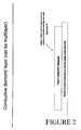
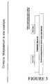
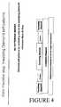
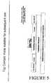
- FIGS. 1-5are schematic representations of the steps necessary to fabricate a substantially all diamond or all diamond transistor.
- any of the thin-film forms of diamond mentioned aboveapply to this invention, the description will refer mostly to UNCD.
- the reduced roughness of UNCD, HOPD, and nanocrystalline diamondindicate that these types of thin film diamond may be the best candidates for such a device if fabricated with a non-single crystal diamond substrate. If a single crystal diamond substrate is used, the use of homoepitaxial diamond layers will be enabled, and a very high-quality device will result.
- homoepitaxial diamondcan only be grown on single crystal diamond.
- This inventionmakes use of this fact in order to produce a type of self-aligned transistor, that is a transistor manufactured without seeding if all diamond or with minimum seeding if a non-diamond substrate is used.
- an appropriate substrateis chosen, and this can be non-diamond, such as a Si wafer with an insulating layer of SiO2 on the surface, any other type of insulating substrate that can withstand the diamond deposition process—it can even be insulating single crystal diamond; 2) if non-diamond, this substrate is treated with any “seeding” process to enable diamond growth; 3) a conductive diamond layer is deposited on the substrate using any diamond deposition process (e.g.
- this conductive layeris patterned (for example, using standard oxygen reactive ion etching), if device isolation is desired—alternatively, the “seeding” process in step 2) can itself be patterned if using a non-diamond substrate, so the resulting conductive diamond layer is already patterned as grown; 5) source and drain contacts are formed on the conductive diamond layer by any process (e.g.
- This inventionincludes devices made with any electrically conductive diamond, either p-type (such as boron doped polycrystalline diamond or, possibly, boron-doped UNCD or n-type (such as phosphorous doped polycrystalline diamond or nitrogen doped UNCD, and any diamond that is insulating (i.e. intrinsic diamond, or fully hydrogen-doped UNCD or nanocrystalline diamond).
- p-typesuch as boron doped polycrystalline diamond or, possibly, boron-doped UNCD or n-type (such as phosphorous doped polycrystalline diamond or nitrogen doped UNCD, and any diamond that is insulating (i.e. intrinsic diamond, or fully hydrogen-doped UNCD or nanocrystalline diamond).
- the key to this inventionis the idea of using high-temperature metal contacts for the source and drain, that these contacts are deposited after the first diamond layer is deposited, and the fact that subsequent insulating diamond layers will grow on the initial conductive diamond layer, but not the contacts—thereby making the device self-aligned and eliminating a
- An all-diamond transistoroperates in a stable fashion at very high temperatures (at which normal Si-based devices would fail due to dopant diffusion or other types of material failure), in highly corrosive environments, and is biocompatible (within the limits of the contact metals used).
- An all diamond transistorhas extremely good electrical characteristics depending on the quality of the diamond used, and is an efficient way to drive other diamond-based devices, including micro-mechanical systems (MEMS).
- MEMSmicro-mechanical systems
- the materials used for the device contactsshould fulfill two requirements: not melt at the temperatures reached during diamond deposition (e.g. ⁇ 900° C., or lower for lower temperature diamond growth processes) and make good electrical contacts to the conductive diamond layer.
- Diamond filmsin particular films with low surface roughnesses such as UNCD and nanocrystalline diamond, are useful for use in MEMS and similar other devices.
- the ability to make electronics out of the same films and using the same processing stepsenable particularly affordable on-board electronics to drive MEMS devices (such as chemical sensors or RF switches).
- Another advantage of this inventionis that fabrication is simplified with such a device as is described here, as diamond etching steps are reduced, and the process does not require the deposition of a gate oxide. This is key, as the insulating layer for thin film transistors is usually an oxide; however, growing oxide on diamond is actually very difficult, as the oxygen used during such thin film growth processes etches the diamond very effectively.
- a thick layer of nitrogen-doped UNCD(deposited by microwave plasma enhanced CVD with the following conditions: 20% N gas, 1.4% CH 4 gas, and 79.6% Ar gas, at a total pressure of 150 mbar and a temperature of 900C) was deposited on a Si wafer (with one micron of thermal oxide previously grown on top to make it electrically insulating), and the wafer was pretreated in a methanol plus diamond nanopowder solution (ultrasonicated for 30 minutes) in order to provide nucleation sites for the UNCD. Shadow masking was then used to deposit Mo contacts via sputtering, and a hydrogen-doped UNCD layer deposited on top.
- the hydrogen-doped UNCDonly grew on the underlying nitrogen-doped electrically conducting diamond layer, but not on the contact metal.
- the deviceswere tested using a room-temperature probe station. It was confirmed that all of the devices leaked readily through the gate (i.e. through the hydrogen-doped UNCD), indicating that the hydrogen-doped UNCD used here did not, in fact, have the requirements for an electronically insulating layer. All other aspects of the device fabrication worked properly. We believe that significant residual nitrogen in the growth chamber (confirmed with optical emission spectroscopy) hindered the passivation of the grain boundary defects with hydrogen, causing the failure of the gate contact.
- One alternative for a substantially all diamond transistoris to provide an electrically insulating substrate includes SiO 2 and an electrically conducting diamond layer of nitrogen doped UNCD less than about 20 nm thick, said electrically insulating diamond layer being nanocrystalline diamond with contacts of Ti or Mo or alloys thereof and a gate of Ti or Mo or alloys thereof or Au.
- the conductive layerif it is desired for it to be as thin as possible, is to first deposit a layer of nano-, polycrystalline, or HOD, insulating diamond on a Si, SiO 2 , or other substrate. Then, the n- or p-doped UNCD (or other conductive diamond) nucleates directly on that initial insulating polycrystalline layer much better than it does on nanopowder-seeded substrates. A very thin conductive layer (less than about 20 nanometers (nm)) is achieved, and the device works better (i.e. achieves device saturation more easily). The rest of the steps would be the same.
- the most preferred all diamond transistoris (an electrically insulating substrate of homoepitaxial diamond, an electrically conductive boron doped UNCD layer less than about 10 nm thick on the electrically insulating substrate of homoepitaxial diamond, a Mo source contact and a Mo drain contact on the electrically conductive boron doped UNCD layer, a self-aligned nanocrystalline diamond layer less than about 500 nm thick in contact with the electrically conductive boron doped UNCD layer, and a Ti/Au gate contact on the self-aligned nanocrystalline diamond layer.
Landscapes
- Engineering & Computer Science (AREA)
- Manufacturing & Machinery (AREA)
- Physics & Mathematics (AREA)
- Condensed Matter Physics & Semiconductors (AREA)
- General Physics & Mathematics (AREA)
- Computer Hardware Design (AREA)
- Microelectronics & Electronic Packaging (AREA)
- Power Engineering (AREA)
- Chemical & Material Sciences (AREA)
- Materials Engineering (AREA)
- Crystallography & Structural Chemistry (AREA)
- Thin Film Transistor (AREA)
- Electrodes Of Semiconductors (AREA)
- Crystals, And After-Treatments Of Crystals (AREA)
Abstract
Description
- This application, pursuant to 37 C.F.R. 1.78©, claims priority based on provisional application Ser. No. 60/609,386 filed on Sep. 13, 2004.
- The United States Government has rights in this invention pursuant to Contract No. W-31-109-ENG-38 between the U.S. Department of Energy (DOE) and The University of Chicago representing Argonne National Laboratory.
- Thin film diamond has been termed many things, from polycrystalline to nanocrystalline to “ultra” nanocrystalline (UNCD). All forms of diamond can be grown via different growth processes, (such as chemical vapor deposition processes including plasma enhanced or hot-wire), and all are applicable here.
- A homoepitaxial single crystal diamond film is a perfect single crystal diamond, and can only be grown on a single crystal diamond substrate. If a similar process is used with a non-diamond substrate, polycrystalline diamond is formed. Depending on the growth parameters used, such films have different preferred crystalline orientations, grain sizes, surface roughness, and quality. If the preferred orientation of such films can be controlled via special substrate layers, or modifications to the growth process, as to promote certain crystal faces with a preferred texture, “highly oriented polycrystalline diamond”, or HOPD, can be produced. This film is a polycrystalline diamond, large-grained material with much lower surface roughness, all as is known in the art.
- If the initial nucleation density of the substrate is particularly high, and the film grown limited in thickness, a very fine-grained polycrystalline diamond can be grown. The key is that the thickness must be kept very small as to limit lateral and competitive grain growth. Such films have been termed “nanocrystalline” diamond (NCD), although the grain sizes can vary from hundreds of nanometers to larger. The key difference with this type of film, other than the much larger numbers of grain boundaries per area, is the benefit of much reduced surface roughness as long as the film thickness is limited. Finally, an extremely fine-grained diamond material, with an extremely large number of grain boundaries, can be produced by altering the diamond thin film growth process. Such material may or may not be equiaxed crystalline, but the surface roughness is extremely low and does not vary with thickness. This material has been termed “ultra” nanocrystalline diamond, or UNCD, in order to delineate it from the “nanocrystalline” diamond above. The grain sizes in this case are between 2 and 5 nm wide, and do not increase with film thickness. Of note for this application, UNCD does show unusual extremely high n-type conductivity when doped with nitrogen, as opposed to the other forms of thin-film diamond discussed above. UNCD has been reported in the patent and scientific literature by inventors and authors at Argonne National Laboratory and others. The invention described here can use any of the forms of diamond described above, as long as they can be made either electrically conductive (via doping, either p- or n-type) or electrically insulating (intrinsic diamond is highly insulating; hydrogen or another passivant may be needed to remove defects from grain boundaries). Different types of diamond thin film can be used within the same device.
- Accordingly, a principal object of the present invention is to provide a substantially all diamond transistor or an all diamond transistor and a method of making same.
- Another object of the present invention is to provide a substantially all diamond transistor, comprising an electrically insulating substrate, an electrically conductive diamond layer on the electrically insulating substrate, a source contact and a drain contact on the electrically conductive diamond layer, an electrically insulating diamond layer in contact with the electrically conductive diamond layer, and a gate contact on the electrically insulating diamond layer.
- Another object of the present invention is to provide a method of making a substantially all diamond self-aligned gate transistor, comprising providing an electrically insulating substrate, depositing an electrically conductive diamond layer on the electrically insulating substrate, establishing a source contact and a drain contact on the electrically conductive diamond layer, depositing an electrically insulating diamond layer in contact with the electrically conductive diamond layer, and providing a gate contact on the electrically insulating diamond layer.
- A further object of the invention is to provide a substantially all diamond transistor, comprising an electrically insulating substrate, an electrically conductive diamond layer less than about 20 nm thick on the electrically insulating substrate, a source contact and a drain contact on the electrically conductive diamond layer, a self-aligned electrically insulating diamond layer less than about 500 nm thick in contact with the electrically conductive diamond layer, and a gate contact on the electrically insulating diamond layer.
- A final object of the invention is to provide a substantially all diamond transistor, comprising an electrically insulating substrate of homoepitaxial diamond, an electrically conductive boron doped UNCD layer less than about 10 nm thick on the electrically insulating substrate of homoepitaxial diamond, a Mo source contact and a Mo drain contact on the electrically conductive boron doped UNCD layer, a self-aligned nanocrystalline diamond layer less than about 500 nm thick in contact with the electrically conductive boron doped UNCD layer, and a Ti/Au gate contact on the self-aligned nanocrystalline diamond layer.
- The invention consists of certain novel features and a combination of parts hereinafter fully described, illustrated in the accompanying drawings, and particularly pointed out in the appended claims, it being understood that various changes in the details may be made without departing from the spirit, or sacrificing any of the advantages of the present invention.
FIGS. 1-5 are schematic representations of the steps necessary to fabricate a substantially all diamond or all diamond transistor.- Although any of the thin-film forms of diamond mentioned above apply to this invention, the description will refer mostly to UNCD. The reduced roughness of UNCD, HOPD, and nanocrystalline diamond indicate that these types of thin film diamond may be the best candidates for such a device if fabricated with a non-single crystal diamond substrate. If a single crystal diamond substrate is used, the use of homoepitaxial diamond layers will be enabled, and a very high-quality device will result.
- All of the types of diamond listed above have the limitation of nucleation hindered growth. When depositing any of these films on a non-diamond substrate, the substrate must be “seeded”; this process usually entails the application of diamond powder to the surface of the substrate, by either an ultrasound solution of physical abrasion. There are also plasma treatments (“bias enhanced nucleation”) and other ways of “seeding” the substrate. A key phenomenon of import to this invention is that thin film diamond will grow on other forms of diamond, without a seeding step; UNCD can grow on nanocrystalline diamond, nanocrystalline diamond can be grown on UNCD, UNCD can be grown even on single crystal diamond, etc., with a near-perfect nucleation step. The only limitation is that homoepitaxial diamond can only be grown on single crystal diamond. This invention makes use of this fact in order to produce a type of self-aligned transistor, that is a transistor manufactured without seeding if all diamond or with minimum seeding if a non-diamond substrate is used.
- The device and method of this invention described here involves the following steps: 1) an appropriate substrate is chosen, and this can be non-diamond, such as a Si wafer with an insulating layer of SiO2 on the surface, any other type of insulating substrate that can withstand the diamond deposition process—it can even be insulating single crystal diamond; 2) if non-diamond, this substrate is treated with any “seeding” process to enable diamond growth; 3) a conductive diamond layer is deposited on the substrate using any diamond deposition process (e.g. forms of chemical vapor deposition including microwave plasma-enhanced and hot-wire); 4) (optional) this conductive layer is patterned (for example, using standard oxygen reactive ion etching), if device isolation is desired—alternatively, the “seeding” process in step 2) can itself be patterned if using a non-diamond substrate, so the resulting conductive diamond layer is already patterned as grown; 5) source and drain contacts are formed on the conductive diamond layer by any process (e.g. sputtering, chemical vapor deposition), patterned (deposited through a shadow mask, or patterned post-growth using typical processes), and these contacts must make good Ohmic contact to the conductive diamond layer, and must have high enough melting temperatures to withstand the next step; 6) insulating diamond is deposited over the entire substrate—it will grow where the conductive diamond is exposed, but not on the metal contacts; 7) final top gate contacts are made on the insulating diamond layer. These contacts need to have melting temperatures high enough to withstand whatever temperatures the device will be exposed to during use—as this is the final step, they do not need to be able to withstand the diamond growth processes.
- This invention includes devices made with any electrically conductive diamond, either p-type (such as boron doped polycrystalline diamond or, possibly, boron-doped UNCD or n-type (such as phosphorous doped polycrystalline diamond or nitrogen doped UNCD, and any diamond that is insulating (i.e. intrinsic diamond, or fully hydrogen-doped UNCD or nanocrystalline diamond). The key to this invention is the idea of using high-temperature metal contacts for the source and drain, that these contacts are deposited after the first diamond layer is deposited, and the fact that subsequent insulating diamond layers will grow on the initial conductive diamond layer, but not the contacts—thereby making the device self-aligned and eliminating a processing step.
- An all-diamond transistor operates in a stable fashion at very high temperatures (at which normal Si-based devices would fail due to dopant diffusion or other types of material failure), in highly corrosive environments, and is biocompatible (within the limits of the contact metals used). An all diamond transistor has extremely good electrical characteristics depending on the quality of the diamond used, and is an efficient way to drive other diamond-based devices, including micro-mechanical systems (MEMS). To that end, the materials used for the device contacts should fulfill two requirements: not melt at the temperatures reached during diamond deposition (e.g. ˜900° C., or lower for lower temperature diamond growth processes) and make good electrical contacts to the conductive diamond layer. For nitrogen-doped UNCD, we have shown that all metals used to date make excellent Ohmic contacts, and so Mo has been used here due to the high melting point of the material. Other high temperature metals, such as, but not limited to, Ti and its alloys, Mo alloys, metal carbides, and metallic ceramics work as well, provided they are good electrical conductors and have the requisite melting points. Forming Ohmic contacts to non-UNCD forms of conductive diamond is more challenging, but can be accomplished with carbide forming metals, and high temperature or ion-bombardment treatments by those of ordinary skill in the art.
- The use of an all-diamond thin film transistor is useful for other reasons. Diamond films, in particular films with low surface roughnesses such as UNCD and nanocrystalline diamond, are useful for use in MEMS and similar other devices. The ability to make electronics out of the same films and using the same processing steps enable particularly affordable on-board electronics to drive MEMS devices (such as chemical sensors or RF switches). Another advantage of this invention is that fabrication is simplified with such a device as is described here, as diamond etching steps are reduced, and the process does not require the deposition of a gate oxide. This is key, as the insulating layer for thin film transistors is usually an oxide; however, growing oxide on diamond is actually very difficult, as the oxygen used during such thin film growth processes etches the diamond very effectively. While it is possible to engineer the use of oxides on diamond with the applications of other barrier films and processes, the procedure becomes much more expensive and time consuming. The use of a non-oxygen containing growth process for the insulating layer is of great interest for diamond electronics, and the use of a diamond layer itself would perhaps yield the best results in terms of film growth on an existing diamond film. Theoretically, pure diamond is the best electrical insulator.
- Using intrinsic undoped nano- or polycrystalline diamond (or HOPD) as the gate insulator is acceptable, as is undoped UNCD.
- The fabrication of an all-electrically conducting diamond thin film transistor was attempted. A thick layer of nitrogen-doped UNCD (deposited by microwave plasma enhanced CVD with the following conditions: 20% N gas, 1.4% CH4gas, and 79.6% Ar gas, at a total pressure of 150 mbar and a temperature of 900C) was deposited on a Si wafer (with one micron of thermal oxide previously grown on top to make it electrically insulating), and the wafer was pretreated in a methanol plus diamond nanopowder solution (ultrasonicated for 30 minutes) in order to provide nucleation sites for the UNCD. Shadow masking was then used to deposit Mo contacts via sputtering, and a hydrogen-doped UNCD layer deposited on top. As predicted, the hydrogen-doped UNCD only grew on the underlying nitrogen-doped electrically conducting diamond layer, but not on the contact metal. The devices were tested using a room-temperature probe station. It was confirmed that all of the devices leaked readily through the gate (i.e. through the hydrogen-doped UNCD), indicating that the hydrogen-doped UNCD used here did not, in fact, have the requirements for an electronically insulating layer. All other aspects of the device fabrication worked properly. We believe that significant residual nitrogen in the growth chamber (confirmed with optical emission spectroscopy) hindered the passivation of the grain boundary defects with hydrogen, causing the failure of the gate contact.
- The use of a different type of diamond layer for an insulating layer is straightforward. One such growth process would use a mostly hydrogen plasma, with ˜1% methane, using higher gas flows, a lower total pressure, and an unheated or cooled substrate stage if using microwave enhanced chemical vapor deposition (the effective temperature of the substrate during growth would still be about 800° C., the hydrogen plasma heats up the substrate much more than the argon one used for electrically conducting diamond.) Alternatively, hot-wire chemical vapor deposition or radio-frequency plasma enhanced chemical vapor deposition could be used, along with any alternative ways to deposit diamond thin films. This invention does not depend on the use of any one type of diamond growth process. All other steps would be the same.
- One alternative for a substantially all diamond transistor is to provide an electrically insulating substrate includes SiO2and an electrically conducting diamond layer of nitrogen doped UNCD less than about 20 nm thick, said electrically insulating diamond layer being nanocrystalline diamond with contacts of Ti or Mo or alloys thereof and a gate of Ti or Mo or alloys thereof or Au.
- Another alternative for the conductive layer, if it is desired for it to be as thin as possible, is to first deposit a layer of nano-, polycrystalline, or HOD, insulating diamond on a Si, SiO2, or other substrate. Then, the n- or p-doped UNCD (or other conductive diamond) nucleates directly on that initial insulating polycrystalline layer much better than it does on nanopowder-seeded substrates. A very thin conductive layer (less than about 20 nanometers (nm)) is achieved, and the device works better (i.e. achieves device saturation more easily). The rest of the steps would be the same. Finally, if a very high quality device is desired, one can start with an insulating single crystal diamond, and grow very thin homoepitaxial conductive and insulating layers (less than about 500 nm, preferably less than about 200 nm) for the device. This results in the highest quality, (and most expensive), device.
- The most preferred all diamond transistor is (an electrically insulating substrate of homoepitaxial diamond, an electrically conductive boron doped UNCD layer less than about 10 nm thick on the electrically insulating substrate of homoepitaxial diamond, a Mo source contact and a Mo drain contact on the electrically conductive boron doped UNCD layer, a self-aligned nanocrystalline diamond layer less than about 500 nm thick in contact with the electrically conductive boron doped UNCD layer, and a Ti/Au gate contact on the self-aligned nanocrystalline diamond layer.
- While there has been disclosed what is considered to be the preferred embodiment of the present invention, it is understood that various changes in the details may be made without departing from the spirit, or sacrificing any of the advantages of the present invention.
Claims (21)
Priority Applications (1)
| Application Number | Priority Date | Filing Date | Title |
|---|---|---|---|
| US11/226,703US7394103B2 (en) | 2004-09-13 | 2005-09-13 | All diamond self-aligned thin film transistor |
Applications Claiming Priority (2)
| Application Number | Priority Date | Filing Date | Title |
|---|---|---|---|
| US60938604P | 2004-09-13 | 2004-09-13 | |
| US11/226,703US7394103B2 (en) | 2004-09-13 | 2005-09-13 | All diamond self-aligned thin film transistor |
Publications (2)
| Publication Number | Publication Date |
|---|---|
| US20060060864A1true US20060060864A1 (en) | 2006-03-23 |
| US7394103B2 US7394103B2 (en) | 2008-07-01 |
Family
ID=36073007
Family Applications (1)
| Application Number | Title | Priority Date | Filing Date |
|---|---|---|---|
| US11/226,703Expired - Fee RelatedUS7394103B2 (en) | 2004-09-13 | 2005-09-13 | All diamond self-aligned thin film transistor |
Country Status (1)
| Country | Link |
|---|---|
| US (1) | US7394103B2 (en) |
Cited By (17)
| Publication number | Priority date | Publication date | Assignee | Title |
|---|---|---|---|---|
| US20070257265A1 (en)* | 2006-05-03 | 2007-11-08 | The University Of Chicago | Use of tungsten interlayer to enhance the initial nucleation and conformality of ultrananocrystalline diamond (UNCD) thin films |
| US20080073646A1 (en)* | 2006-08-11 | 2008-03-27 | Akhan Technologies,Inc. | P-channel nanocrystalline diamond field effect transistor |
| US20080134960A1 (en)* | 2005-06-20 | 2008-06-12 | Nippon Telegraph And Telephone Corporation | Diamond semiconductor element and process for producing the same |
| US20080246368A1 (en)* | 2006-11-30 | 2008-10-09 | Uchicago Argonne, Llc | Integration of dissimilar materials for advanced multfunctional devices |
| US20110186942A1 (en)* | 2008-01-04 | 2011-08-04 | Advanced Diamond Technologies | Controlling diamond film surfaces and layering |
| US20120279852A1 (en)* | 2008-01-24 | 2012-11-08 | Michael Zach | Nanowire and Microwire Fabrication Technique and Product |
| US8404313B1 (en) | 2006-03-22 | 2013-03-26 | University Of South Florida | Synthesis of nanocrystalline diamond fibers |
| US20130175546A1 (en)* | 2012-01-06 | 2013-07-11 | Akhan Technologies, Inc. | Diamond Semiconductor System and Method |
| US20150041810A1 (en)* | 2011-08-30 | 2015-02-12 | Sandia Corporation | Method to fabricate micro and nano diamond devices |
| US20150060947A1 (en)* | 2013-08-30 | 2015-03-05 | The Government Of The United States Of America, As Represented By The Secretary Of The Navy | Transistor with Diamond Gate |
| US20150228727A1 (en)* | 2012-08-17 | 2015-08-13 | National Institute Of Advance Industrial Science And Technology | Diamond semiconductor device and method for manufacturing same |
| WO2015179421A1 (en)* | 2014-05-20 | 2015-11-26 | Uchicago Argonne, Llc | Low-stress doped ultrananocrystalline diamond |
| US20160064500A1 (en)* | 2014-09-03 | 2016-03-03 | Applied Materials, Inc. | Nanocrystaline diamond carbon film for 3d nand hardmask application |
| US9484474B1 (en) | 2015-07-02 | 2016-11-01 | Uchicago Argonne, Llc | Ultrananocrystalline diamond contacts for electronic devices |
| US9741561B2 (en) | 2015-07-10 | 2017-08-22 | Uchicago Argonne, Llc | Transparent nanocrystalline diamond coatings and devices |
| JP2020024211A (en)* | 2015-08-07 | 2020-02-13 | フラウンホーファー・ユー・エス・エイ・インコーポレイテッドFraunhofer Usa, Inc. | Apparatus and method for detecting trace metals at conductive diamond electrodes |
| US11522055B2 (en)* | 2018-01-15 | 2022-12-06 | National Institute Of Advanced Industrial Science And Technology | Stack comprising single-crystal diamond substrate |
Families Citing this family (2)
| Publication number | Priority date | Publication date | Assignee | Title |
|---|---|---|---|---|
| US7989261B2 (en)* | 2008-12-22 | 2011-08-02 | Raytheon Company | Fabricating a gallium nitride device with a diamond layer |
| US9685522B1 (en)* | 2016-04-08 | 2017-06-20 | Globalfoundries Inc. | Forming uniform WF metal layers in gate areas of nano-sheet structures |
Citations (14)
| Publication number | Priority date | Publication date | Assignee | Title |
|---|---|---|---|---|
| US4981818A (en)* | 1990-02-13 | 1991-01-01 | General Electric Company | Polycrystalline CVD diamond substrate for single crystal epitaxial growth of semiconductors |
| US5107315A (en)* | 1990-03-13 | 1992-04-21 | Kabushiki Kaisha Kobe Seiko Sho | Mis type diamond field-effect transistor with a diamond insulator undercoat |
| US5173761A (en)* | 1991-01-28 | 1992-12-22 | Kobe Steel Usa Inc., Electronic Materials Center | Semiconducting polycrystalline diamond electronic devices employing an insulating diamond layer |
| US5254862A (en)* | 1991-08-14 | 1993-10-19 | Kobe Steel U.S.A., Inc. | Diamond field-effect transistor with a particular boron distribution profile |
| US5371383A (en)* | 1993-05-14 | 1994-12-06 | Kobe Steel Usa Inc. | Highly oriented diamond film field-effect transistor |
| US5382809A (en)* | 1992-09-14 | 1995-01-17 | Sumitomo Electric Industries, Ltd. | Semiconductor device including semiconductor diamond |
| US5382822A (en)* | 1992-09-25 | 1995-01-17 | Siemens Aktiengesellschaft | Metal-insulator semiconductor field-effect transistor |
| US5420443A (en)* | 1991-12-20 | 1995-05-30 | Kobe Development Corporation | Microelectronic structure having an array of diamond structures on a nondiamond substrate and associated fabrication methods |
| US5455432A (en)* | 1994-10-11 | 1995-10-03 | Kobe Steel Usa | Diamond semiconductor device with carbide interlayer |
| US5491348A (en)* | 1993-05-14 | 1996-02-13 | Kobe Steel Usa, Inc. | Highly-oriented diamond film field-effect transistor |
| US5523588A (en)* | 1993-09-28 | 1996-06-04 | Kabushiki Kaisha Kobe Seiko Sho | Diamond film field effect transistor with self aligned source and drain regions |
| US5633513A (en)* | 1992-11-24 | 1997-05-27 | Kabushiki Kaisha Kobe Seiko Sho | Diamond film field effect transistor |
| US6492309B1 (en)* | 2000-03-31 | 2002-12-10 | 3M Innovative Properties Company | Fluorinated solvent compositions containing hydrogen fluoride |
| US20050110024A1 (en)* | 2003-11-25 | 2005-05-26 | Board Of Trustees Of Michigan State University | Boron-doped nanocrystalline diamond |
Family Cites Families (1)
| Publication number | Priority date | Publication date | Assignee | Title |
|---|---|---|---|---|
| JPH07321317A (en)* | 1994-05-25 | 1995-12-08 | Sony Corp | Mis field effect transistor and its manufacture |
- 2005
- 2005-09-13USUS11/226,703patent/US7394103B2/ennot_activeExpired - Fee Related
Patent Citations (15)
| Publication number | Priority date | Publication date | Assignee | Title |
|---|---|---|---|---|
| US4981818A (en)* | 1990-02-13 | 1991-01-01 | General Electric Company | Polycrystalline CVD diamond substrate for single crystal epitaxial growth of semiconductors |
| US5107315A (en)* | 1990-03-13 | 1992-04-21 | Kabushiki Kaisha Kobe Seiko Sho | Mis type diamond field-effect transistor with a diamond insulator undercoat |
| US5173761A (en)* | 1991-01-28 | 1992-12-22 | Kobe Steel Usa Inc., Electronic Materials Center | Semiconducting polycrystalline diamond electronic devices employing an insulating diamond layer |
| US5254862A (en)* | 1991-08-14 | 1993-10-19 | Kobe Steel U.S.A., Inc. | Diamond field-effect transistor with a particular boron distribution profile |
| US5420443A (en)* | 1991-12-20 | 1995-05-30 | Kobe Development Corporation | Microelectronic structure having an array of diamond structures on a nondiamond substrate and associated fabrication methods |
| US5382809A (en)* | 1992-09-14 | 1995-01-17 | Sumitomo Electric Industries, Ltd. | Semiconductor device including semiconductor diamond |
| US5382822A (en)* | 1992-09-25 | 1995-01-17 | Siemens Aktiengesellschaft | Metal-insulator semiconductor field-effect transistor |
| US5633513A (en)* | 1992-11-24 | 1997-05-27 | Kabushiki Kaisha Kobe Seiko Sho | Diamond film field effect transistor |
| US5371383A (en)* | 1993-05-14 | 1994-12-06 | Kobe Steel Usa Inc. | Highly oriented diamond film field-effect transistor |
| US5491348A (en)* | 1993-05-14 | 1996-02-13 | Kobe Steel Usa, Inc. | Highly-oriented diamond film field-effect transistor |
| US5506422A (en)* | 1993-05-14 | 1996-04-09 | Kobe Steel Usa, Inc. | MOIS junction for use in a diamond electronic device |
| US5523588A (en)* | 1993-09-28 | 1996-06-04 | Kabushiki Kaisha Kobe Seiko Sho | Diamond film field effect transistor with self aligned source and drain regions |
| US5455432A (en)* | 1994-10-11 | 1995-10-03 | Kobe Steel Usa | Diamond semiconductor device with carbide interlayer |
| US6492309B1 (en)* | 2000-03-31 | 2002-12-10 | 3M Innovative Properties Company | Fluorinated solvent compositions containing hydrogen fluoride |
| US20050110024A1 (en)* | 2003-11-25 | 2005-05-26 | Board Of Trustees Of Michigan State University | Boron-doped nanocrystalline diamond |
Cited By (47)
| Publication number | Priority date | Publication date | Assignee | Title |
|---|---|---|---|---|
| US8221548B2 (en) | 2005-06-20 | 2012-07-17 | Nippon Telegraph And Telephone Corporation | Diamond semiconductor element and process for producing the same |
| US8487319B2 (en) | 2005-06-20 | 2013-07-16 | Nippon Telegraph And Telephone Corporation | Diamond semiconductor element and process for producing the same |
| US20080134960A1 (en)* | 2005-06-20 | 2008-06-12 | Nippon Telegraph And Telephone Corporation | Diamond semiconductor element and process for producing the same |
| US8486816B2 (en) | 2005-06-20 | 2013-07-16 | Nippon Telegraph And Telephone Corporation | Diamond semiconductor element and process for producing the same |
| US20090261347A1 (en)* | 2005-06-20 | 2009-10-22 | Nippon Telegraph And Telephone Corporation | Diamond semiconductor element and process for producing the same |
| US8328936B2 (en) | 2005-06-20 | 2012-12-11 | Nippon Telegraph And Telephone Corporation | Producing a diamond semiconductor by implanting dopant using ion implantation |
| US20100289030A9 (en)* | 2005-06-20 | 2010-11-18 | Nippon Telegraph And Telephone Corporation | Diamond semiconductor element and process for producing the same |
| US20110070694A1 (en)* | 2005-06-20 | 2011-03-24 | Nippon Telegraph And Telephone Corporation | Diamond semiconductor element and process for producing the same |
| US20110068352A1 (en)* | 2005-06-20 | 2011-03-24 | Nippon Telegraph And Telephone Corporation | Diamond semiconductor element and process for producing the same |
| US8242511B2 (en)* | 2005-06-20 | 2012-08-14 | Nippon Telegraph And Telephone Corporation | Field effect transistor using diamond and process for producing the same |
| US8404313B1 (en) | 2006-03-22 | 2013-03-26 | University Of South Florida | Synthesis of nanocrystalline diamond fibers |
| US20070257265A1 (en)* | 2006-05-03 | 2007-11-08 | The University Of Chicago | Use of tungsten interlayer to enhance the initial nucleation and conformality of ultrananocrystalline diamond (UNCD) thin films |
| GB2454844A (en)* | 2006-08-11 | 2009-05-27 | Akhan Technologies Inc | P-Channel nanocrystalline diamond field effect transistor |
| WO2008019404A3 (en)* | 2006-08-11 | 2008-11-06 | Akhan Technologies Inc | P-channel nanocrystalline diamond field effect transistor |
| US20080073646A1 (en)* | 2006-08-11 | 2008-03-27 | Akhan Technologies,Inc. | P-channel nanocrystalline diamond field effect transistor |
| US7791201B2 (en)* | 2006-11-30 | 2010-09-07 | Uchicago Argonne, Llc | Integration of dissimilar materials for advanced multifunctional devices |
| US20080246368A1 (en)* | 2006-11-30 | 2008-10-09 | Uchicago Argonne, Llc | Integration of dissimilar materials for advanced multfunctional devices |
| US8232559B2 (en)* | 2008-01-04 | 2012-07-31 | Advanced Diamond Technologies, Inc. | Controlling diamond film surfaces and layering |
| US20110186942A1 (en)* | 2008-01-04 | 2011-08-04 | Advanced Diamond Technologies | Controlling diamond film surfaces and layering |
| US20120279852A1 (en)* | 2008-01-24 | 2012-11-08 | Michael Zach | Nanowire and Microwire Fabrication Technique and Product |
| US8652615B2 (en)* | 2008-01-24 | 2014-02-18 | Wisys Technology Foundation | Nanowire and microwire fabrication technique and product |
| US20150041810A1 (en)* | 2011-08-30 | 2015-02-12 | Sandia Corporation | Method to fabricate micro and nano diamond devices |
| US9620596B2 (en)* | 2011-08-30 | 2017-04-11 | Sandia Corporation | Method to fabricate micro and nano diamond devices |
| US10546749B2 (en)* | 2012-01-06 | 2020-01-28 | Akhan Semiconductor, Inc. | Diamond semiconductor system and method |
| TWI615943B (en)* | 2012-01-06 | 2018-02-21 | 阿克漢科技公司 | Diamond semiconductor system and method thereof |
| US20150155160A1 (en)* | 2012-01-06 | 2015-06-04 | Khan Adam | Diamond Semiconductor System and Method |
| US20130175546A1 (en)* | 2012-01-06 | 2013-07-11 | Akhan Technologies, Inc. | Diamond Semiconductor System and Method |
| TWI711153B (en)* | 2012-01-06 | 2020-11-21 | 美商阿克漢科技公司 | Diamond semiconductor system and method |
| TWI672795B (en)* | 2012-01-06 | 2019-09-21 | 美商阿克漢科技公司 | Diamond semiconductor system and method |
| US20150228727A1 (en)* | 2012-08-17 | 2015-08-13 | National Institute Of Advance Industrial Science And Technology | Diamond semiconductor device and method for manufacturing same |
| US9478619B2 (en)* | 2012-08-17 | 2016-10-25 | National Institute Of Advanced Industrial Science And Technology | Diamond semiconductor device and method for manufacturing same |
| US9331163B2 (en)* | 2013-08-30 | 2016-05-03 | The United States Of America, As Represented By The Secretary Of The Navy | Transistor with diamond gate |
| US20150060947A1 (en)* | 2013-08-30 | 2015-03-05 | The Government Of The United States Of America, As Represented By The Secretary Of The Navy | Transistor with Diamond Gate |
| US9475690B2 (en) | 2014-05-20 | 2016-10-25 | Uchicago Argonne, Llc | Low-stress doped ultrananocrystalline diamond |
| WO2015179421A1 (en)* | 2014-05-20 | 2015-11-26 | Uchicago Argonne, Llc | Low-stress doped ultrananocrystalline diamond |
| TWI618225B (en)* | 2014-09-03 | 2018-03-11 | 應用材料股份有限公司 | Nanocrystalline diamond carbon film for 3D NAND hard mask applications |
| US9865464B2 (en) | 2014-09-03 | 2018-01-09 | Applied Materials, Inc. | Nanocrystalline diamond carbon film for 3D NAND hardmask application |
| US9502262B2 (en)* | 2014-09-03 | 2016-11-22 | Applied Materials, Inc. | Nanocrystalline diamond carbon film for 3D NAND hardmask application |
| US20160064500A1 (en)* | 2014-09-03 | 2016-03-03 | Applied Materials, Inc. | Nanocrystaline diamond carbon film for 3d nand hardmask application |
| US9842958B2 (en)* | 2015-07-02 | 2017-12-12 | Uchicago Argonne, Llc | Ultrananocrystalline diamond contacts for electronic devices |
| US20170047468A1 (en)* | 2015-07-02 | 2017-02-16 | Brookhaven Science Associates, Llc | Ultrananocrystalline diamond contacts for electronic devices |
| WO2017004400A1 (en)* | 2015-07-02 | 2017-01-05 | Uchicago Argonne, Llc | Ultrananocrystalline diamond contacts for electronic devices |
| US9484474B1 (en) | 2015-07-02 | 2016-11-01 | Uchicago Argonne, Llc | Ultrananocrystalline diamond contacts for electronic devices |
| US9741561B2 (en) | 2015-07-10 | 2017-08-22 | Uchicago Argonne, Llc | Transparent nanocrystalline diamond coatings and devices |
| US10410860B2 (en) | 2015-07-10 | 2019-09-10 | Uchicago Argonne, Llc | Transparent nanocrystalline diamond coatings and devices |
| JP2020024211A (en)* | 2015-08-07 | 2020-02-13 | フラウンホーファー・ユー・エス・エイ・インコーポレイテッドFraunhofer Usa, Inc. | Apparatus and method for detecting trace metals at conductive diamond electrodes |
| US11522055B2 (en)* | 2018-01-15 | 2022-12-06 | National Institute Of Advanced Industrial Science And Technology | Stack comprising single-crystal diamond substrate |
Also Published As
| Publication number | Publication date |
|---|---|
| US7394103B2 (en) | 2008-07-01 |
Similar Documents
| Publication | Publication Date | Title |
|---|---|---|
| US7394103B2 (en) | All diamond self-aligned thin film transistor | |
| KR101465452B1 (en) | Method of graphene manufacturing | |
| US7981721B2 (en) | Diamond transistor and method of manufacture thereof | |
| US10253426B2 (en) | Method for manufacturing diamond substrate | |
| CN108400157B (en) | Substrate for diamond film formation and method for manufacturing diamond substrate using same | |
| EP0779666A2 (en) | Semiconductor device and method of fabricating semiconductor device | |
| JP2008539575A5 (en) | ||
| US9347149B2 (en) | Method for growing epitaxial diamond | |
| EP3211658B1 (en) | Method for manufacturing diamond substrate | |
| US20190296113A1 (en) | Method of making a gallium nitride device | |
| Subramanian et al. | The effect of growth rate control on the morphology of nanocrystalline diamond | |
| Stoner et al. | Hall effect measurements on boron‐doped, highly oriented diamond films grown on silicon via microwave plasma chemical vapor deposition | |
| US8158011B2 (en) | Method of fabrication of cubic boron nitride conical microstructures | |
| Jiang et al. | Approach of selective nucleation and epitaxy of diamond films on Si (100) | |
| EP2023381A1 (en) | Method of selectively forming atomically flat plane on diamond surface, diamond substrate produced by the method, and semiconductor element employing the same | |
| US5155559A (en) | High temperature refractory silicide rectifying contact | |
| KR0147498B1 (en) | Low temperature selective growth of silicon or silicon alloys | |
| Jiang et al. | Deposition of heteroepitaxial diamond films on 2 in silicon substrates | |
| JP2008071896A (en) | Metal-insulating film-silicon carbide semiconductor structure | |
| Kwak et al. | Boron‐Doped Single‐Crystal Diamond Growth on Heteroepitaxial Diamond Substrate Using Microwave Plasma Chemical Vapor Deposition | |
| Kim et al. | Effect of cyclic process on the {100}‐oriented texture growth of diamond film | |
| Sone et al. | Formation of low pressure chemically vapour deposited W thin film on silicon dioxide for gate electrode application | |
| JP4070305B2 (en) | Method for forming silicon carbide crystal film | |
| JPS59177919A (en) | Selective growth of thin film | |
| Achiq et al. | Effects of pre-hydrogenation on the relaxation and bandgap variation of thermally nanocrystallized silicon layers |
Legal Events
| Date | Code | Title | Description |
|---|---|---|---|
| AS | Assignment | Owner name:CHICAGO, UNIVERSITY OF, ILLINOIS Free format text:ASSIGNMENT OF ASSIGNORS INTEREST;ASSIGNOR:GERBI, JENNIFER;REEL/FRAME:016853/0397 Effective date:20051114 | |
| AS | Assignment | Owner name:UNITED STATES DEPARTMENT OF ENERGY, DISTRICT OF CO Free format text:CONFIRMATORY LICENSE;ASSIGNOR:THE UNIVERSITY OF CHICAGO;REEL/FRAME:017416/0149 Effective date:20051103 | |
| AS | Assignment | Owner name:U CHICAGO ARGONNE LLC,ILLINOIS Free format text:ASSIGNMENT OF ASSIGNORS INTEREST;ASSIGNOR:UNIVERSITY OF CHICAGO, THE;REEL/FRAME:018385/0618 Effective date:20060925 Owner name:U CHICAGO ARGONNE LLC, ILLINOIS Free format text:ASSIGNMENT OF ASSIGNORS INTEREST;ASSIGNOR:UNIVERSITY OF CHICAGO, THE;REEL/FRAME:018385/0618 Effective date:20060925 | |
| FPAY | Fee payment | Year of fee payment:4 | |
| REMI | Maintenance fee reminder mailed | ||
| LAPS | Lapse for failure to pay maintenance fees | ||
| STCH | Information on status: patent discontinuation | Free format text:PATENT EXPIRED DUE TO NONPAYMENT OF MAINTENANCE FEES UNDER 37 CFR 1.362 | |
| FP | Lapsed due to failure to pay maintenance fee | Effective date:20160701 |