US20060057304A1 - Biased pulse DC reactive sputtering of oxide films - Google Patents
Biased pulse DC reactive sputtering of oxide filmsDownload PDFInfo
- Publication number
- US20060057304A1 US20060057304A1US11/191,643US19164305AUS2006057304A1US 20060057304 A1US20060057304 A1US 20060057304A1US 19164305 AUS19164305 AUS 19164305AUS 2006057304 A1US2006057304 A1US 2006057304A1
- Authority
- US
- United States
- Prior art keywords
- target
- substrate
- reactor
- pulsed
- deposited
- Prior art date
- Legal status (The legal status is an assumption and is not a legal conclusion. Google has not performed a legal analysis and makes no representation as to the accuracy of the status listed.)
- Granted
Links
- 238000005546reactive sputteringMethods0.000titledescription4
- 239000000758substrateSubstances0.000claimsabstractdescription181
- 238000000034methodMethods0.000claimsabstractdescription118
- 230000008569processEffects0.000claimsabstractdescription77
- 239000000463materialSubstances0.000claimsabstractdescription46
- 238000000151depositionMethods0.000claimsdescription127
- 229910052782aluminiumInorganic materials0.000claimsdescription44
- 229910052710siliconInorganic materials0.000claimsdescription44
- 239000007789gasSubstances0.000claimsdescription41
- 239000000203mixtureSubstances0.000claimsdescription35
- QVGXLLKOCUKJST-UHFFFAOYSA-Natomic oxygenChemical compound[O]QVGXLLKOCUKJST-UHFFFAOYSA-N0.000claimsdescription29
- 239000001301oxygenSubstances0.000claimsdescription29
- 229910052760oxygenInorganic materials0.000claimsdescription29
- 230000005291magnetic effectEffects0.000claimsdescription26
- XKRFYHLGVUSROY-UHFFFAOYSA-NArgonChemical compound[Ar]XKRFYHLGVUSROY-UHFFFAOYSA-N0.000claimsdescription25
- 229910052691ErbiumInorganic materials0.000claimsdescription19
- 229910052786argonInorganic materials0.000claimsdescription13
- 229910052761rare earth metalInorganic materials0.000claimsdescription13
- -1rare-earth ionsChemical class0.000claimsdescription13
- 229910052769YtterbiumInorganic materials0.000claimsdescription12
- 239000000919ceramicSubstances0.000claimsdescription6
- 238000001513hot isostatic pressingMethods0.000claimsdescription5
- 229910052693EuropiumInorganic materials0.000claimsdescription4
- 229910052737goldInorganic materials0.000claimsdescription4
- 239000000843powderSubstances0.000claimsdescription4
- 229910052709silverInorganic materials0.000claimsdescription4
- 229910052684CeriumInorganic materials0.000claimsdescription3
- 229910052688GadoliniumInorganic materials0.000claimsdescription3
- 229910052765LutetiumInorganic materials0.000claimsdescription3
- 229910052779NeodymiumInorganic materials0.000claimsdescription3
- 229910052777PraseodymiumInorganic materials0.000claimsdescription3
- 229910052772SamariumInorganic materials0.000claimsdescription3
- 229910052787antimonyInorganic materials0.000claimsdescription3
- 229910052785arsenicInorganic materials0.000claimsdescription3
- 238000000889atomisationMethods0.000claimsdescription3
- 229910002091carbon monoxideInorganic materials0.000claimsdescription3
- 229910052733galliumInorganic materials0.000claimsdescription3
- 229910052732germaniumInorganic materials0.000claimsdescription3
- 150000004820halidesChemical class0.000claimsdescription3
- 229910052745leadInorganic materials0.000claimsdescription3
- 229910052698phosphorusInorganic materials0.000claimsdescription3
- 229910052718tinInorganic materials0.000claimsdescription3
- 229910052725zincInorganic materials0.000claimsdescription3
- 229910052776ThoriumInorganic materials0.000claimsdescription2
- 238000010408sweepingMethods0.000claims6
- IJGRMHOSHXDMSA-UHFFFAOYSA-NAtomic nitrogenChemical compoundN#NIJGRMHOSHXDMSA-UHFFFAOYSA-N0.000claims4
- 238000001914filtrationMethods0.000claims4
- 229910052775ThuliumInorganic materials0.000claims2
- 229910052757nitrogenInorganic materials0.000claims2
- 229910052771TerbiumInorganic materials0.000claims1
- 238000004544sputter depositionMethods0.000abstractdescription33
- 230000003287optical effectEffects0.000abstractdescription31
- 230000000694effectsEffects0.000abstractdescription7
- 239000010408filmSubstances0.000description158
- 230000008021depositionEffects0.000description118
- 239000010410layerSubstances0.000description74
- 239000011162core materialSubstances0.000description32
- 230000002441reversible effectEffects0.000description25
- 238000005253claddingMethods0.000description24
- VYPSYNLAJGMNEJ-UHFFFAOYSA-NSilicium dioxideChemical compoundO=[Si]=OVYPSYNLAJGMNEJ-UHFFFAOYSA-N0.000description22
- 235000012431wafersNutrition0.000description21
- 230000003628erosive effectEffects0.000description18
- XUIMIQQOPSSXEZ-UHFFFAOYSA-NSiliconChemical compound[Si]XUIMIQQOPSSXEZ-UHFFFAOYSA-N0.000description16
- 239000010703siliconSubstances0.000description16
- PNEYBMLMFCGWSK-UHFFFAOYSA-Naluminium oxideInorganic materials[O-2].[O-2].[O-2].[Al+3].[Al+3]PNEYBMLMFCGWSK-UHFFFAOYSA-N0.000description15
- XAGFODPZIPBFFR-UHFFFAOYSA-NaluminiumChemical compound[Al]XAGFODPZIPBFFR-UHFFFAOYSA-N0.000description13
- 231100000614poisonToxicity0.000description13
- 238000005424photoluminescenceMethods0.000description12
- 239000002574poisonSubstances0.000description12
- 150000002500ionsChemical class0.000description9
- 239000000377silicon dioxideSubstances0.000description9
- UYAHIZSMUZPPFV-UHFFFAOYSA-NerbiumChemical compound[Er]UYAHIZSMUZPPFV-UHFFFAOYSA-N0.000description8
- 238000010168coupling processMethods0.000description7
- 239000011521glassSubstances0.000description7
- 238000004519manufacturing processMethods0.000description7
- 230000008859changeEffects0.000description6
- 238000006243chemical reactionMethods0.000description6
- 230000008878couplingEffects0.000description6
- 238000005859coupling reactionMethods0.000description6
- 230000007423decreaseEffects0.000description6
- 239000002019doping agentSubstances0.000description6
- 239000002184metalSubstances0.000description6
- 230000002829reductive effectEffects0.000description6
- 239000000126substanceSubstances0.000description6
- 238000009825accumulationMethods0.000description5
- 238000005229chemical vapour depositionMethods0.000description5
- 239000012792core layerSubstances0.000description5
- 238000005137deposition processMethods0.000description5
- 238000005530etchingMethods0.000description5
- 238000001755magnetron sputter depositionMethods0.000description5
- 229910052751metalInorganic materials0.000description5
- 238000005240physical vapour depositionMethods0.000description5
- 235000012239silicon dioxideNutrition0.000description5
- 239000013077target materialSubstances0.000description5
- 229910045601alloyInorganic materials0.000description4
- 239000000956alloySubstances0.000description4
- 238000000137annealingMethods0.000description4
- 230000001143conditioned effectEffects0.000description4
- 239000000835fiberSubstances0.000description4
- 238000012545processingMethods0.000description4
- 238000001552radio frequency sputter depositionMethods0.000description4
- 230000015572biosynthetic processEffects0.000description3
- 238000004140cleaningMethods0.000description3
- 239000002131composite materialSubstances0.000description3
- 230000003750conditioning effectEffects0.000description3
- 230000005281excited stateEffects0.000description3
- 230000004907fluxEffects0.000description3
- 239000011261inert gasSubstances0.000description3
- 238000003780insertionMethods0.000description3
- 230000037431insertionEffects0.000description3
- 230000000670limiting effectEffects0.000description3
- 238000007254oxidation reactionMethods0.000description3
- 238000000206photolithographyMethods0.000description3
- 238000005086pumpingMethods0.000description3
- 150000002910rare earth metalsChemical class0.000description3
- 239000004065semiconductorSubstances0.000description3
- 238000000926separation methodMethods0.000description3
- ZOXJGFHDIHLPTG-UHFFFAOYSA-NBoronChemical compound[B]ZOXJGFHDIHLPTG-UHFFFAOYSA-N0.000description2
- 229910052796boronInorganic materials0.000description2
- 229910052681coesiteInorganic materials0.000description2
- 238000004891communicationMethods0.000description2
- 239000000470constituentSubstances0.000description2
- 238000001816coolingMethods0.000description2
- 229910052906cristobaliteInorganic materials0.000description2
- 230000003247decreasing effectEffects0.000description2
- 230000007547defectEffects0.000description2
- 238000007599dischargingMethods0.000description2
- 238000009826distributionMethods0.000description2
- BHEPBYXIRTUNPN-UHFFFAOYSA-Nhydridophosphorus(.) (triplet)Chemical compound[PH]BHEPBYXIRTUNPN-UHFFFAOYSA-N0.000description2
- 239000012212insulatorSubstances0.000description2
- 238000005259measurementMethods0.000description2
- 230000007246mechanismEffects0.000description2
- 229910001092metal group alloyInorganic materials0.000description2
- 150000004767nitridesChemical class0.000description2
- 230000003647oxidationEffects0.000description2
- 239000010453quartzSubstances0.000description2
- 238000010791quenchingMethods0.000description2
- 230000000171quenching effectEffects0.000description2
- 229910052682stishoviteInorganic materials0.000description2
- 239000010409thin filmSubstances0.000description2
- 230000007704transitionEffects0.000description2
- 229910052905tridymiteInorganic materials0.000description2
- NAWDYIZEMPQZHO-UHFFFAOYSA-NytterbiumChemical compound[Yb]NAWDYIZEMPQZHO-UHFFFAOYSA-N0.000description2
- CJRJTCMSQLEPFQ-UHFFFAOYSA-N6-catChemical compoundClC1=CC=C2CC(N)CCC2=C1CJRJTCMSQLEPFQ-UHFFFAOYSA-N0.000description1
- MYMOFIZGZYHOMD-UHFFFAOYSA-NDioxygenChemical compoundO=OMYMOFIZGZYHOMD-UHFFFAOYSA-N0.000description1
- 229910019142PO4Inorganic materials0.000description1
- 239000011149active materialSubstances0.000description1
- 239000003513alkaliSubstances0.000description1
- 229910052783alkali metalInorganic materials0.000description1
- 150000001340alkali metalsChemical class0.000description1
- 229910000323aluminium silicateInorganic materials0.000description1
- 229910021417amorphous siliconInorganic materials0.000description1
- 230000003321amplificationEffects0.000description1
- 238000013459approachMethods0.000description1
- 239000002585baseSubstances0.000description1
- 230000009286beneficial effectEffects0.000description1
- 230000008901benefitEffects0.000description1
- 230000005540biological transmissionEffects0.000description1
- 239000005388borosilicate glassSubstances0.000description1
- 150000004649carbonic acid derivativesChemical class0.000description1
- 125000002091cationic groupChemical group0.000description1
- 230000005591charge neutralizationEffects0.000description1
- 150000001875compoundsChemical class0.000description1
- 238000011109contaminationMethods0.000description1
- 229910052593corundumInorganic materials0.000description1
- 238000002425crystallisationMethods0.000description1
- 230000008025crystallizationEffects0.000description1
- 238000000280densificationMethods0.000description1
- 238000013461designMethods0.000description1
- 230000001627detrimental effectEffects0.000description1
- HNPSIPDUKPIQMN-UHFFFAOYSA-Ndioxosilane;oxo(oxoalumanyloxy)alumaneChemical compoundO=[Si]=O.O=[Al]O[Al]=OHNPSIPDUKPIQMN-UHFFFAOYSA-N0.000description1
- 229910001882dioxygenInorganic materials0.000description1
- 230000009977dual effectEffects0.000description1
- 238000010893electron trapMethods0.000description1
- 238000011067equilibrationMethods0.000description1
- 238000011049fillingMethods0.000description1
- 150000002222fluorine compoundsChemical class0.000description1
- 238000010438heat treatmentMethods0.000description1
- 230000007062hydrolysisEffects0.000description1
- 238000006460hydrolysis reactionMethods0.000description1
- 230000006872improvementEffects0.000description1
- 239000011810insulating materialSubstances0.000description1
- 230000010354integrationEffects0.000description1
- 238000010849ion bombardmentMethods0.000description1
- 238000005342ion exchangeMethods0.000description1
- 238000001459lithographyMethods0.000description1
- 238000004020luminiscence typeMethods0.000description1
- 150000001247metal acetylidesChemical class0.000description1
- 239000007769metal materialSubstances0.000description1
- 229910044991metal oxideInorganic materials0.000description1
- 150000004706metal oxidesChemical class0.000description1
- 238000003199nucleic acid amplification methodMethods0.000description1
- 239000013307optical fiberSubstances0.000description1
- 238000013386optimize processMethods0.000description1
- TWNQGVIAIRXVLR-UHFFFAOYSA-Noxo(oxoalumanyloxy)alumaneChemical compoundO=[Al]O[Al]=OTWNQGVIAIRXVLR-UHFFFAOYSA-N0.000description1
- 239000002245particleSubstances0.000description1
- 238000000059patterningMethods0.000description1
- 230000002688persistenceEffects0.000description1
- 235000021317phosphateNutrition0.000description1
- 150000003013phosphoric acid derivativesChemical class0.000description1
- 230000000704physical effectEffects0.000description1
- 230000007096poisonous effectEffects0.000description1
- WCWKKSOQLQEJTE-UHFFFAOYSA-Npraseodymium(3+)Chemical compound[Pr+3]WCWKKSOQLQEJTE-UHFFFAOYSA-N0.000description1
- 230000002035prolonged effectEffects0.000description1
- 239000000376reactantSubstances0.000description1
- 230000035945sensitivityEffects0.000description1
- 150000004760silicatesChemical class0.000description1
- 229910052814silicon oxideInorganic materials0.000description1
- 238000005245sinteringMethods0.000description1
- 239000007787solidSubstances0.000description1
- 230000006641stabilisationEffects0.000description1
- 238000011105stabilizationMethods0.000description1
- 230000007847structural defectEffects0.000description1
- 150000003467sulfuric acid derivativesChemical class0.000description1
- 239000002344surface layerSubstances0.000description1
- 230000003746surface roughnessEffects0.000description1
- 230000009897systematic effectEffects0.000description1
- 150000003568thioethersChemical class0.000description1
- 238000009827uniform distributionMethods0.000description1
- 229910001845yogo sapphireInorganic materials0.000description1
Images


Classifications
- C—CHEMISTRY; METALLURGY
- C23—COATING METALLIC MATERIAL; COATING MATERIAL WITH METALLIC MATERIAL; CHEMICAL SURFACE TREATMENT; DIFFUSION TREATMENT OF METALLIC MATERIAL; COATING BY VACUUM EVAPORATION, BY SPUTTERING, BY ION IMPLANTATION OR BY CHEMICAL VAPOUR DEPOSITION, IN GENERAL; INHIBITING CORROSION OF METALLIC MATERIAL OR INCRUSTATION IN GENERAL
- C23C—COATING METALLIC MATERIAL; COATING MATERIAL WITH METALLIC MATERIAL; SURFACE TREATMENT OF METALLIC MATERIAL BY DIFFUSION INTO THE SURFACE, BY CHEMICAL CONVERSION OR SUBSTITUTION; COATING BY VACUUM EVAPORATION, BY SPUTTERING, BY ION IMPLANTATION OR BY CHEMICAL VAPOUR DEPOSITION, IN GENERAL
- C23C14/00—Coating by vacuum evaporation, by sputtering or by ion implantation of the coating forming material
- C23C14/22—Coating by vacuum evaporation, by sputtering or by ion implantation of the coating forming material characterised by the process of coating
- C23C14/34—Sputtering
- C23C14/3435—Applying energy to the substrate during sputtering
- C23C14/345—Applying energy to the substrate during sputtering using substrate bias
- C—CHEMISTRY; METALLURGY
- C23—COATING METALLIC MATERIAL; COATING MATERIAL WITH METALLIC MATERIAL; CHEMICAL SURFACE TREATMENT; DIFFUSION TREATMENT OF METALLIC MATERIAL; COATING BY VACUUM EVAPORATION, BY SPUTTERING, BY ION IMPLANTATION OR BY CHEMICAL VAPOUR DEPOSITION, IN GENERAL; INHIBITING CORROSION OF METALLIC MATERIAL OR INCRUSTATION IN GENERAL
- C23C—COATING METALLIC MATERIAL; COATING MATERIAL WITH METALLIC MATERIAL; SURFACE TREATMENT OF METALLIC MATERIAL BY DIFFUSION INTO THE SURFACE, BY CHEMICAL CONVERSION OR SUBSTITUTION; COATING BY VACUUM EVAPORATION, BY SPUTTERING, BY ION IMPLANTATION OR BY CHEMICAL VAPOUR DEPOSITION, IN GENERAL
- C23C14/00—Coating by vacuum evaporation, by sputtering or by ion implantation of the coating forming material
- C23C14/0021—Reactive sputtering or evaporation
- C23C14/0036—Reactive sputtering
- C—CHEMISTRY; METALLURGY
- C23—COATING METALLIC MATERIAL; COATING MATERIAL WITH METALLIC MATERIAL; CHEMICAL SURFACE TREATMENT; DIFFUSION TREATMENT OF METALLIC MATERIAL; COATING BY VACUUM EVAPORATION, BY SPUTTERING, BY ION IMPLANTATION OR BY CHEMICAL VAPOUR DEPOSITION, IN GENERAL; INHIBITING CORROSION OF METALLIC MATERIAL OR INCRUSTATION IN GENERAL
- C23C—COATING METALLIC MATERIAL; COATING MATERIAL WITH METALLIC MATERIAL; SURFACE TREATMENT OF METALLIC MATERIAL BY DIFFUSION INTO THE SURFACE, BY CHEMICAL CONVERSION OR SUBSTITUTION; COATING BY VACUUM EVAPORATION, BY SPUTTERING, BY ION IMPLANTATION OR BY CHEMICAL VAPOUR DEPOSITION, IN GENERAL
- C23C14/00—Coating by vacuum evaporation, by sputtering or by ion implantation of the coating forming material
- C23C14/06—Coating by vacuum evaporation, by sputtering or by ion implantation of the coating forming material characterised by the coating material
- C23C14/08—Oxides
- C23C14/081—Oxides of aluminium, magnesium or beryllium
- C—CHEMISTRY; METALLURGY
- C23—COATING METALLIC MATERIAL; COATING MATERIAL WITH METALLIC MATERIAL; CHEMICAL SURFACE TREATMENT; DIFFUSION TREATMENT OF METALLIC MATERIAL; COATING BY VACUUM EVAPORATION, BY SPUTTERING, BY ION IMPLANTATION OR BY CHEMICAL VAPOUR DEPOSITION, IN GENERAL; INHIBITING CORROSION OF METALLIC MATERIAL OR INCRUSTATION IN GENERAL
- C23C—COATING METALLIC MATERIAL; COATING MATERIAL WITH METALLIC MATERIAL; SURFACE TREATMENT OF METALLIC MATERIAL BY DIFFUSION INTO THE SURFACE, BY CHEMICAL CONVERSION OR SUBSTITUTION; COATING BY VACUUM EVAPORATION, BY SPUTTERING, BY ION IMPLANTATION OR BY CHEMICAL VAPOUR DEPOSITION, IN GENERAL
- C23C14/00—Coating by vacuum evaporation, by sputtering or by ion implantation of the coating forming material
- C23C14/06—Coating by vacuum evaporation, by sputtering or by ion implantation of the coating forming material characterised by the coating material
- C23C14/10—Glass or silica
- C—CHEMISTRY; METALLURGY
- C23—COATING METALLIC MATERIAL; COATING MATERIAL WITH METALLIC MATERIAL; CHEMICAL SURFACE TREATMENT; DIFFUSION TREATMENT OF METALLIC MATERIAL; COATING BY VACUUM EVAPORATION, BY SPUTTERING, BY ION IMPLANTATION OR BY CHEMICAL VAPOUR DEPOSITION, IN GENERAL; INHIBITING CORROSION OF METALLIC MATERIAL OR INCRUSTATION IN GENERAL
- C23C—COATING METALLIC MATERIAL; COATING MATERIAL WITH METALLIC MATERIAL; SURFACE TREATMENT OF METALLIC MATERIAL BY DIFFUSION INTO THE SURFACE, BY CHEMICAL CONVERSION OR SUBSTITUTION; COATING BY VACUUM EVAPORATION, BY SPUTTERING, BY ION IMPLANTATION OR BY CHEMICAL VAPOUR DEPOSITION, IN GENERAL
- C23C14/00—Coating by vacuum evaporation, by sputtering or by ion implantation of the coating forming material
- C23C14/22—Coating by vacuum evaporation, by sputtering or by ion implantation of the coating forming material characterised by the process of coating
- C23C14/34—Sputtering
- C23C14/3407—Cathode assembly for sputtering apparatus, e.g. Target
- C23C14/3414—Metallurgical or chemical aspects of target preparation, e.g. casting, powder metallurgy
- C—CHEMISTRY; METALLURGY
- C23—COATING METALLIC MATERIAL; COATING MATERIAL WITH METALLIC MATERIAL; CHEMICAL SURFACE TREATMENT; DIFFUSION TREATMENT OF METALLIC MATERIAL; COATING BY VACUUM EVAPORATION, BY SPUTTERING, BY ION IMPLANTATION OR BY CHEMICAL VAPOUR DEPOSITION, IN GENERAL; INHIBITING CORROSION OF METALLIC MATERIAL OR INCRUSTATION IN GENERAL
- C23C—COATING METALLIC MATERIAL; COATING MATERIAL WITH METALLIC MATERIAL; SURFACE TREATMENT OF METALLIC MATERIAL BY DIFFUSION INTO THE SURFACE, BY CHEMICAL CONVERSION OR SUBSTITUTION; COATING BY VACUUM EVAPORATION, BY SPUTTERING, BY ION IMPLANTATION OR BY CHEMICAL VAPOUR DEPOSITION, IN GENERAL
- C23C14/00—Coating by vacuum evaporation, by sputtering or by ion implantation of the coating forming material
- C23C14/22—Coating by vacuum evaporation, by sputtering or by ion implantation of the coating forming material characterised by the process of coating
- C23C14/34—Sputtering
- C23C14/35—Sputtering by application of a magnetic field, e.g. magnetron sputtering
- C23C14/354—Introduction of auxiliary energy into the plasma
- C—CHEMISTRY; METALLURGY
- C23—COATING METALLIC MATERIAL; COATING MATERIAL WITH METALLIC MATERIAL; CHEMICAL SURFACE TREATMENT; DIFFUSION TREATMENT OF METALLIC MATERIAL; COATING BY VACUUM EVAPORATION, BY SPUTTERING, BY ION IMPLANTATION OR BY CHEMICAL VAPOUR DEPOSITION, IN GENERAL; INHIBITING CORROSION OF METALLIC MATERIAL OR INCRUSTATION IN GENERAL
- C23C—COATING METALLIC MATERIAL; COATING MATERIAL WITH METALLIC MATERIAL; SURFACE TREATMENT OF METALLIC MATERIAL BY DIFFUSION INTO THE SURFACE, BY CHEMICAL CONVERSION OR SUBSTITUTION; COATING BY VACUUM EVAPORATION, BY SPUTTERING, BY ION IMPLANTATION OR BY CHEMICAL VAPOUR DEPOSITION, IN GENERAL
- C23C14/00—Coating by vacuum evaporation, by sputtering or by ion implantation of the coating forming material
- C23C14/58—After-treatment
- C23C14/5806—Thermal treatment
- C—CHEMISTRY; METALLURGY
- C23—COATING METALLIC MATERIAL; COATING MATERIAL WITH METALLIC MATERIAL; CHEMICAL SURFACE TREATMENT; DIFFUSION TREATMENT OF METALLIC MATERIAL; COATING BY VACUUM EVAPORATION, BY SPUTTERING, BY ION IMPLANTATION OR BY CHEMICAL VAPOUR DEPOSITION, IN GENERAL; INHIBITING CORROSION OF METALLIC MATERIAL OR INCRUSTATION IN GENERAL
- C23C—COATING METALLIC MATERIAL; COATING MATERIAL WITH METALLIC MATERIAL; SURFACE TREATMENT OF METALLIC MATERIAL BY DIFFUSION INTO THE SURFACE, BY CHEMICAL CONVERSION OR SUBSTITUTION; COATING BY VACUUM EVAPORATION, BY SPUTTERING, BY ION IMPLANTATION OR BY CHEMICAL VAPOUR DEPOSITION, IN GENERAL
- C23C14/00—Coating by vacuum evaporation, by sputtering or by ion implantation of the coating forming material
- C23C14/58—After-treatment
- C23C14/5873—Removal of material
- G—PHYSICS
- G02—OPTICS
- G02B—OPTICAL ELEMENTS, SYSTEMS OR APPARATUS
- G02B6/00—Light guides; Structural details of arrangements comprising light guides and other optical elements, e.g. couplings
- G02B6/10—Light guides; Structural details of arrangements comprising light guides and other optical elements, e.g. couplings of the optical waveguide type
- G02B6/12—Light guides; Structural details of arrangements comprising light guides and other optical elements, e.g. couplings of the optical waveguide type of the integrated circuit kind
- G02B6/13—Integrated optical circuits characterised by the manufacturing method
- G02B6/132—Integrated optical circuits characterised by the manufacturing method by deposition of thin films
- H—ELECTRICITY
- H01—ELECTRIC ELEMENTS
- H01J—ELECTRIC DISCHARGE TUBES OR DISCHARGE LAMPS
- H01J37/00—Discharge tubes with provision for introducing objects or material to be exposed to the discharge, e.g. for the purpose of examination or processing thereof
- H01J37/32—Gas-filled discharge tubes
- H01J37/32009—Arrangements for generation of plasma specially adapted for examination or treatment of objects, e.g. plasma sources
- H01J37/32412—Plasma immersion ion implantation
- H—ELECTRICITY
- H01—ELECTRIC ELEMENTS
- H01J—ELECTRIC DISCHARGE TUBES OR DISCHARGE LAMPS
- H01J37/00—Discharge tubes with provision for introducing objects or material to be exposed to the discharge, e.g. for the purpose of examination or processing thereof
- H01J37/32—Gas-filled discharge tubes
- H01J37/34—Gas-filled discharge tubes operating with cathodic sputtering
Definitions
- the present inventionrelates to deposition of oxide and oxynitride films and, in particular, to deposition of oxide and oxynitride films by pulsed DC reactive sputtering.
- insulating materials and especially optical materialsis technologically important in several areas including production of optical devices and production of semiconductor devices.
- doped alumina silicatescan be utilized as high dielectric insulators.
- Planar devicessuch as optical waveguides, couplers, splitters, and amplifiers, fabricated on planar substrates, like those commonly used for integrated circuits, and configured to receive and process signals from optical fibers are highly desirable. Such devices hold promise for integrated optical and electronic signal processing on a single semiconductor-like substance.
- planar optical waveguides and amplifiersare well known, as described, for example, in U.S. Pat. No. 5,119,460 and U.S. Pat. No. 5,563,979 to Bruce et al., U.S. Pat. No. 5,613,995 to Bhandarkar et al., U.S. Pat. No. 5,900,057 to Buchal et al., and U.S. Pat. No. 5,107,538 to Benton et al., to cite only a few.
- These devicesvery generally, include a core region, typically bar shaped, of a certain refractive index surrounded by a cladding region of a lower refractive index.
- the core regionincludes a certain concentration of a dopant, typically a rare earth ion such as an erbium or praseodymium ion which, when pumped by a laser, fluoresces, for example, in the 1550 nm and 1300 nm wavelength ranges used for optical communication, to amplify the optical signal passing through the core.
- a dopanttypically a rare earth ion such as an erbium or praseodymium ion which, when pumped by a laser, fluoresces, for example, in the 1550 nm and 1300 nm wavelength ranges used for optical communication, to amplify the optical signal passing through the core.
- planar optical devicesmay be fabricated by process sequences including forming a layer of cladding material on a substrate; forming a layer of core material on the layer of cladding mater; patterning the core layer using a photolighotgraphic mask and an etching process to form a core ridge; and covering the core ridge with an upper cladding layer.
- the performance of these planar optical devicesdepends sensitively on the value and uniformity of the refractive index of the core region and of the cladding region, and particularly on the difference in refractive index, ⁇ n, between the regions.
- ⁇ nshould be carefully controlled, for example to values within about 1%, and the refractive index of both core and cladding need to be highly uniform, for some applications at the fewer than parts per thousand level.
- doped materials forming the core region of planar optical amplifiersit is important that the dopant be uniformly distributed so as to avoid non-radiative quenching or radiative quenching, for example by upconversion.
- the refractive index and other desirable properties of the core and cladding regionssuch as physical and chemical uniformity, low stress, and high density, depend, of course, on the choice of materials for the devices and on the processes by which they are fabricated.
- silica and refractory oxidessuch as Al 2 O 3 are good candidate materials for planar optical devices. Further, these oxides serve as suitable hosts for rare earth dopants used in optical amplifiers.
- a common material choiceis so-called low temperature glasses, doped with alkali metals, boron, or phosphorous, which have the advantage of requiring lower processing temperatures.
- dopantsare used to modify the refractive index. Methods such as flame hydrolysis, ion exchange for introducing alkali ions in glasses, sputtering, and various chemical vapor deposition processes (CVD) have been used to form films of doped glasses.
- dopantssuch as phosphorous and boron are hygroscopic, and alkalis are undesirable for integration with electronic devices. Control of uniformity of doping in CVD processes can be difficult and CVD deposited films can have structural defects leading to scattering losses when used to guide light. In addition, doped low temperature glasses may require further processing after deposition. A method for eliminating bubbles in thin films of sodium-boro-silicate glass by high temperature sintering is described, for example, in the '995 patent to Bhandarkar et al.
- RF sputteringhas been utilized for deposition of oxide dielectric films.
- RF sputteringutilizes ceramic targets which are typically formed of multiple smaller tiles. Since the tiles can not be made very large, there may be a large problem of arcing between tiles and therefore contamination of the deposited film due to this arcing. Further, the reactors required for RF sputtering tend to be rather complicated. In particular, the engineering of low capacitance efficient RF power distribution to the cathode is difficult in RF systems. Routing of low capacitance forward and return power into a vacuum vessel of the reaction chamber often exposes the power path in such a way that diffuse plasma discharge is allowed under some conditions of impedance tuning of the matching networks.
- a sputtering reactor apparatusfor depositing oxide and oxynitride films is presented. Further, methods for depositing oxide and oxynitride films for optical waveguide devices are also presented.
- a sputtering reactor according to the present inventionincludes a pulsed DC power supply coupled through a filter to a target and a substrate electrode coupled to an RF power supply. A substrate mounted on the substrate electrode is therefore supplied with a bias from the RF power supply.
- the targetcan be a metallic target made of a material to be deposited on the substrate.
- the metallic targetis formed from Al, Si and various rare-earth ions.
- a target with an erbium concentration, for example,can be utilized to deposit a film that can be formed into a waveguide optical amplifier.
- a substratecan be any material and, in some embodiments, is a silicon wafer.
- RF powercan be supplied to the wafer.
- the wafer and the electrodecan be separated by an insulating glass.
- up to about 10 kW of pulsed DC power at a frequency of between about 40 kHz and 350 kHz and a reverse pulse time of up to about 5 ⁇ sis supplied to the target.
- the wafercan be biased with up to about several hundred watts of RF power.
- the temperature of the substratecan be controlled to within about 10° C. and can vary from about ⁇ 50° C. to several hundred degrees C.
- Process gassescan be fed into the reaction chamber of the reactor apparatus.
- the process gassescan include combinations of Ar, N 2 , O 2 , C 2 F 6 , CO 2 , CO and other process gasses.
- deposited layercan be modified by adjusting the composition of the target, the composition and flow rate of the process gasses, the power supplied to the target and the substrate, and the temperature of the substrate.
- the index of refraction of the deposited layerdepends on deposition parameters.
- stresscan be relieved on the substrate by depositing a thin film of material on a back side of the wafer. Films deposited according to the present invention can be utilized to form optical waveguide devices such as multiplexers and rare-earth doped amplifiers.
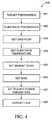
- FIGS. 1A and 1Bshow a pulsed DC sputtering reactor according to the present invention.
- FIG. 2shows a planar view of target utilized in a reactor as shown in FIGS. 1A and 1B .
- FIG. 3shows a cross-section view of an example target utilized in a reactor as shown in FIGS. 1A and 1B .
- FIG. 4shows a flow chart of an embodiment of a process for depositing a film on a substrate according to the present invention.
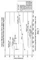
- FIG. 5shows a hysterises curve of target voltage versus oxygen flow rates for an example target in an embodiment of a reactor according to the present invention.
- FIG. 6shows a photo-luminescence and lifetimes of a film deposited in a process according to the present invention as a function of after deposition anneal temperature.
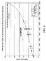
- FIG. 7shows the relationship between the index of refraction of a film as a function of deposited oxide layers according to the present invention and due to oxide build-up on the target.
- FIG. 8shows a graph of the index of refraction of a film deposited according to the present invention as a function of the aluminum content in a composite Al/Si target.
- FIG. 9shows a graph of typical indices of refraction of material layers deposited according to the present invention.
- FIG. 10shows a table of indices of refraction for a silica layer deposited according to the present invention as a function of different process parameters.
- FIG. 11shows the refractive indices as a function of O 2 /Ar ratio utilized in an Alumina process according to the present invention.
- FIG. 12shows the refractive indices as a function of DC pulsed power frequency for an Alumina layer deposited according to the present invention.
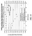
- FIG. 13shows variation in the refractive index over time during repeated depositions from a single target.
- FIG. 14shows variation in refractive index over time for repeated depositions from a target of another material layer according to the present invention.
- FIG. 15shows the variation refractive index over time for repeated depositions from a target of another material layer according to the present invention.
- FIG. 16A through 16Dshows a TEM film deposited according to the present invention.
- FIG. 17shows the transparency of a film deposited according to the present invention.
- FIG. 18shows an uppercladding layer deposited according to the present invention over a multiple-waveguide structure such that the deposited layer is substantially planarized.
- FIG. 19illustrates the deposition of a film over a waveguide structure.
- FIGS. 20 and 21illustrate different etch and deposition rates for deposition of films as a function of the surface angle of the film.
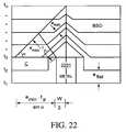
- FIG. 22illustrates calculation of the planarization time for a particular deposition process.
- FIGS. 23 through 25 throughillustrate adjustment of process parameters in order to achieve planarization of a film deposited over a waveguide structure according to the present invention.
- FIG. 26shows the gain characteristics of an erbium doped waveguide amplifier formed of films depositions according to the present invention.
- FIG. 27shows gain, insertion loss of a waveguide with an active core deposited according to the present invention.
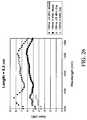
- FIG. 28shows up-conversion constants, and lifetimes of the active core layer of FIG. 27 deposited according to the present invention.
- FIG. 29shows drift in the index of refraction with subsequent depositions for films deposited from a target according to the present invention.
- FIG. 30shows drift in the photoluminescence with subsequent depositions according to the present invention.
- FIG. 31shows drift in the excited state lifetime with subsequent depositions according to the present invention.
- FIG. 32shows stabilization of the index of refraction in subsequent depositions.
- FIG. 33shows the index of refraction of a film formed from a pure silicon target as a function of the ratio of O 2 /N 2 in the process gas.
- Reactive DC magnetron sputtering of nitrides and carbidesis a widely practiced technique, but the reactive dc magnetron sputtering of nonconducting oxides is done rarely. Films such as aluminum oxide are almost impossible to deposit by conventional reactive DC magnetron sputtering due to rapid formation of insulating oxide layers on the target surface. The insulating surfaces charges up and result in arcing during process. This arcing can damage the power supply, produce particles and degrade the properties of deposited oxide films.
- a gain-flattened amplifier formed of films deposited according to the present inventionare described in U.S. application Ser. No. ⁇ Attorney Docket No. M-12652 US ⁇ (the '652 application), filed concurrently with the present disclosure, assigned to the same assignee as is the present invention, herein incorporated by reference in its entirety.
- a mode size converter formed with films deposited according to the present inventionis described in U.S. application Ser. No. ⁇ Attorney Docket No. M-12138 US ⁇ (the '138 application), filed concurrently with the present disclosure, assigned to the same assignee as is the present invention, herein incorporated by reference in its entirety.
- FIG. 1Ashows a schematic of a reactor apparatus 10 for sputtering of material from a target 12 according to the present invention.
- apparatus 10may, for example, be adapted from an AKT-1600 PVD (400 ⁇ 500 mm substrate size) system from Applied Komatsu or an AKT-4300 (600 ⁇ 720 mm substrate size) system from Applied Komatsu, Santa Clara, Calif.
- the AKT-1600 reactorfor example, has three deposition chambers connected by a vacuum transport chamber. These Komatsu reactors can be modified such that pulsed DC power is supplied to the target and RF power is supplied to the substrate during deposition of a material film.
- Apparatus 10includes a target 12 which is electrically coupled through a filter 15 to a pulsed DC power supply 14 .
- target 12is a wide area sputter source target, which provides material to be deposited on substrate 16 .
- Substrate 16is positioned parallel to and opposite target 12 .
- Target 12functions as a cathode when power is applied to it and is equivalently termed a cathode.
- Application of power to target 12creates a plasma 53 .
- Substrate 16is capacitively coupled to an electrode 17 through an insulator 54 .
- Electrode 17can be coupled to an RF power supply 18 .
- Magnet 20is scanned across the top of target 12 .
- the polarity of the power supplied to target 12 by power supply 14oscillates between negative and positive potentials.
- the insulating layer on the surface of target 12is discharged and arcing is prevented.
- the pulsing frequencyexceeds a critical frequency that depend on target material, cathode current and reverse time. High quality oxide films can be made using reactive pulse DC magnetron sputtering in apparatus 10 .
- Pulsed DC power supply 14can be any pulsed DC power supply, for example an AE Pinnacle plus 10K by Advanced Energy, Inc. With this example supply, up to 10 kW of pulsed DC power can be supplied at a frequency of between 0 and 350 KHz.
- the reverse voltageis 10% of the negative target voltage. Utilization of other power supplies will lead to different power characteristics, frequency characteristics and reverse voltage percentages.
- the reverse time on this embodiment of power supply 14can be adjusted between 0 and 5 ⁇ s.
- Filter 15prevents the bias power from power supply 18 from coupling into pulsed DC power supply 14 .
- power supply 18is a 2 MHz RF power supply, for example can be a Nova-25 power supply made by ENI, Colorado Springs, Co.
- filter 15is a 2 MHz band rejection filter.
- the band width of the filtercan be approximately 100 kHz. Filter 15 , therefore, prevents the 2 MHz power from the bias to substrate 16 from damaging power supply 18 .
- both RF and pulsed DC deposited filmsare not fully dense and most likely have columnar structures. These columnar structures are detrimental for optical wave guide applications due to the scattering loss caused by the structure.
- the deposited filmcan be dandified by energetic ion bombardment and the columnar structure can be substantially eliminated.
- target 12can have an active size of about 675.70 ⁇ 582.48 by 4 mm in order to deposit films on substrate 16 that have dimension about 400 ⁇ 500 mm.
- the temperature of substrate 16can be held at between ⁇ 50C and 500C.
- the distance between target 12 and substrate 16can be between about 3 and about 9 cm.
- Process gascan be inserted into the chamber of apparatus 10 at a rate up to about 200 sccm while the pressure in the chamber of apparatus 10 can be held at between about 0.7 and 6 millitorr.
- Magnet 20provides a magnetic field of strength between about 400 and about 600 Gauss directed in the plane of target 12 and is moved across target 12 at a rate of less than about 20-30 sec/scan.
- magnet 20can be a race-track shaped magnet with dimension about 150 mm by 600 mm.
- FIG. 2A top down view of magnet 20 and wide area target 12 is shown in FIG. 2 .
- a film deposited on a substrate positioned on carrier sheet 17 directly opposed to region 52 of target 12has good thickness uniformity.
- Region 52is the region shown in FIG. 1B that is exposed to a uniform plasma condition.
- carrier 17can be coextensive with region 52 .
- Region 24 shown in FIG. 2indicates the area below which both physically and chemically uniform deposition can be achieved, where physical and chemical uniformity provide refractive index uniformity, for example.
- FIG. 2indicates that region 52 of target 12 that provides thickness uniformity is, in general, larger than region 24 of target 12 providing thickness and chemical uniformity. In optimized processes, however, regions 52 and 24 may be coextensive.
- magnet 20extends beyond area 52 in one direction, the Y direction in FIG. 2 , so that scanning is necessary in only one direction, the X direction, to provide a time averaged uniform magnetic field. As shown in FIGS. 1A and 1B , magnet 20 can be scanned over the entire extent of target 12 , which is larger than region 52 of uniform sputter erosion. Magnet 20 is moved in a plane parallel to the plane of target 12 .
- the combination of a uniform target 12 with a target area 52 larger than the area of substrate 16can provide films of highly uniform thickness. Further, the material properties of the film deposited can be highly uniform.
- the conditions of sputtering at the target surfacesuch as the uniformity of erosion, the average temperature of the plasma at the target surface and the equilibration of the target surface with the gas phase ambient of the process are uniform over a region which is greater than or equal to the region to be coated with a uniform film thickness.
- the region of uniform film thicknessis greater than or equal to the region of the film which is to have highly uniform optical properties such as index of refraction, density, transmission or absorptivity.
- Target 12can be formed of any materials, but is typically metallic materials such as, for example, combinations of Al and Si. Therefore, in some embodiments, target 12 includes a metallic target material formed from intermetalic compounds of optical elements such as Si, Al, Er and Yb. Additionally, target 12 can be formed, for example, from materials such as La, Yt, Ag, Au, and Eu. To form optically active films on substrate 16 , target 12 can include rare-earth ions. In some embodiments of target 12 with rare earth ions, the rare earth ions can be pre-alloyed with the metallic host components to form intermetalics. See the '247 application.
- material tilesare formed. These tiles can be mounted on a backing plate to form a target for apparatus 10 .
- FIG. 3Ashows an embodiment of target 12 formed with individual tiles 30 mounted on a cooled backplate 25 .
- the consolidated material of individual tiles 30should first be uniform to the grain size of the powder from which it is formed. It also should be formed into a structural material capable of forming and finishing to a tile shape having a surface roughness on the order of the powder size from which it is consolidated.
- a wide area sputter cathode targetcan be formed from a close packed array of smaller tiles.
- Target 12therefore, may include any number of tiles 30 , for example between 2 to 20 individual tiles 30 .
- Tiles 30are finished to a size so as to provide a margin of non-contact, tile to tile, 29 in FIG. 3A , less than about 0.010′′ to about 0.020′′ or less than half a millimeter so as to eliminate plasma processes between adjacent ones of tiles 30 .
- the distance between tiles 30 of target 12 and the dark space anode or ground shield 19 , in FIG. 1Bcan be somewhat larger so as to provide non contact assembly or provide for thermal expansion tolerance during process chamber conditioning or operation.
- target 12that can be utilized in apparatus 10 according to the present invention include the following targets compositions: (Si/Al/Er/Yb) being about (57.0/41.4/0.8/0.8), (48.9/49/1.6/0.5), (92/8/0/0), (60/40/0/0), (50/50/0/0), (65/35/0/0), (70/30/0,0), and (50,48.5/1.5/0) cat. %, to list only a few. These targets can be referred to as the 0.8/0.8 target, the 1.6/0.5 target, the 92-8 target, the 60-40 target, the 50-50 target, the 65-35 target, the 70-30 target, and the 1.5/0 target, respectively.
- the 0.8/0.8, 1.6/0.5, and 1.5/0 targetscan be made by pre-alloyed targets formed from an atomization and hot-isostatic pressing (HIPing) process as described in the '247 application.
- the remaining targetscan be formed, for example, by HIPing.
- Targets formed from Si, Al, Er and Ybcan have any composition.
- the rare earth contentcan be up to 10 cat. % of the total ion content in the target.
- Rare earth ionsare added to form active layers for amplification.
- Targets utilized in apparatus 10can have any composition and can include ions other than Si, Al, Er and Yb, including: Zn, Ga, Ge, P, As, Sn, Sb, Pb, Ag, Au, and rare earths: Ce, Pr, Nd, Pm, Sm, Eu, Gd, Th, Dy Ho, Er, Tm Yb and Lu.
- Optically useful materials to be deposited onto substrate 16include oxides, fluorides, sulfides, nitrides, phosphates, sulfates, and carbonates, as well as other wide band gap semiconductor materials.
- target 12itself can be chemically uniform and of uniform thickness over an extended area.
- Target 12can be a composite target fabricated from individual tiles, precisely bonded together on a backing plate with minimal separation, as is discussed further with respect to FIG. 3 .
- the mixed intermetalllicscan be plasma sprayed directly onto a backing plate to form target 12 .
- the complete target assemblycan also includes structures for cooling the target, embodiments of which have been described in U.S. Pat. No. 5,565,071 to Demaray et al, and incorporated herein by reference.
- Substrate 16can be a solid, smooth surface.
- substrate 16can be a silicon wafer or a silicon wafer coated with a layer of silicon oxide formed by a chemical vapor deposition process or by a thermal oxidation process.
- substrate 16can be a glass, such as Corning 1737 (Corning Inc., Elmira, N.Y.), a glass-like material, quartz, a metal, a metal oxide, or a plastic material.
- Substrate 16can be supported on a holder or carrier sheet that may be larger than substrate 16 .
- Substrate 16can be electrically biased by power supply 18 .
- the area of wide area target 12can be greater than the area on the carrier sheet on which physically and chemically uniform deposition is accomplished.
- a central region on target 12 , overlying substrate 16can be provided with a very uniform condition of sputter erosion of the target material.
- Uniform target erosionis a consequence of a uniform plasma condition. In the following discussion, all mention of uniform condition of target erosion is taken to be equivalent to uniform plasma condition. Uniform target erosion is evidenced by the persistence of film uniformity throughout an extended target life.
- a uniformly deposited filmcan be defined as a film having a nonuniformity in thickness, when measured at representative points on the entire surface of a substrate wafer, of less than about 5% or 10%.
- Thickness nonuniformityis defined, by convention, as the difference between the minimum and maximum thickness divided by twice the average thickness. If films deposited from a target from which more than about 20% of the weight of the target has been removed continue to exhibit thickness uniformity, then the sputtering process is judged to be in a condition of uniform target erosion for all films deposited during the target life.
- a uniform plasma conditioncan be created in the region between target 12 and substrate 16 in a region overlying substrate 16 .
- a plasma 53can be created in region 51 , which extends under the entire target 12 .
- a central region 52 of target 12can experience a condition of uniform sputter erosion.
- a layer deposited on a substrate placed anywhere below central region 52can then be uniform in thickness and other properties (i.e., dielectric, optical index, or material concentrations).
- region 52 in which deposition provides uniformity of deposited filmcan be larger than the area in which the deposition provides a film with uniform physical or optical properties such as chemical composition or index of refraction.
- target 12is substantially planar in order to provide uniformity in the film deposited on substrate 16 .
- planarity of target 12can mean that all portions of the target surface in region 52 are within a few millimeters of a planar surface, and can be typically within 0.5 mm of a planar surface.
- ⁇ approaches to providing a uniform condition of sputter erosionrely on creating a large uniform magnetic field or a scanning magnetic field that produces a time-averaged, uniform magnetic field.
- rotating magnets or electromagnetscan be utilized to provide wide areas of substantially uniform target erosion.
- a scanning magnet magnetron sourcecan be used to provide a uniform, wide area condition of target erosion.
- apparatus 10can include a scanning magnet magnetron source 20 positioned above target 12 .
- a scanning magnetron sourceused for dc sputtering of metallic films is described in U.S. Pat. No. 5,855,744 to Halsey, et. al., (hereafter '744), which is incorporated herein by reference in its entirety.
- the '744 patentdemonstrates the improvement in thickness uniformity that is achieved by reducing local target erosion due to magnetic effects in the sputtering of a wide area rectangular target. As described in the '744 patent, by reducing the magnetic field intensity at these positions, the local target erosion was decreased and the resulting film thickness nonuniformity was improved from 8%, to 4%, over a rectangular substrate of 400 ⁇ 500 mm.
- the process gas utilized in reactor 10includes an inert gas, typically argon, used as the background sputtering gas. Additionally, with some embodiments of target 12 , reactive components such as, for example, oxygen may be added to the sputtering gas. Other gasses such as N 2 , NH 3 , CO, NO, CO 2 , halide containing gasses other gas-phase reactants can also be utilized.
- the deposition chambercan be operated at low pressure, often between about 0.5 millitorr and 8-10 millitorr. Typical process pressure is below about 3-5 millitorr where there are very few collisions in the gas phase, resulting in a condition of uniform “free molecular” flow.
- the distance d, in FIG. 1A , between target 12 and substrate 16can, in some embodiments, be varied between about 4 cm and about 9 cm.
- a typical target to substrate distance dis about 6 cm.
- the target to substrate distancecan be chosen to optimize the thickness uniformity of the film.
- the film thickness distributionis dome shaped with the thickest region of the film at the center of the substrate.
- the film thicknessis dish shaped with the thickest film formed at the edge of the substrate.
- the substrate temperaturecan be held constant in the range of about ⁇ 40° C. to about 550° C. and can be maintained at a chosen temperature to within about 10° C. by means of preheating substrate 16 and the substrate holder prior to deposition.
- the heat energy impressed upon the substrate by the processcan be conducted away from substrate 16 by cooling the table on which substrate 16 is positioned during the process, as known to those skilled in the art.
- the processis performed under conditions of uniform gas introduction, uniform pumping speed, and uniform application of power to the periphery of the target as known to skilled practitioners.
- the speed at which a scanning magnet 20 can be swept over the entire targetcan be determined such that a layer thickness less than about 5 to 10 ⁇ , corresponding roughly to two to four monolayers of material, is deposited on each scan.
- Magnet 20can be moved at rates up to about 30 sec/one-way scan and typically is moved at a rate of about 4 sec/one-way scan.
- the rate at which material is depositeddepends on the applied power and on the distance d, in FIG. 1A , between the target 12 and the substrate 16 .
- scanning speeds between about 2 sec/one-way scan across the target to 20-30 sec/scanprovide a beneficial layer thickness. Limiting the amount of material deposited in each pass promotes chemical and physical uniformity of the deposited layer.
- Substrate biashas been used previously to planarize RF sputtered deposited quartz films.
- a theoretical model of the mechanism by which substrate bias operates,has been put forward by Ting et al. (J. Vac. Sci. Technol. 15, 1105 (1978)).
- a so-called plasma sheathis formed about the substrate and ions are coupled from the plasma.
- the sheathserves to accelerate ions from the plasma so that they bombard the film as it is deposited, sputtering the film, and forward scattering surface atoms, densifying the film and eliminating columnar structure.
- the effects of adding substrate biasare akin to, but more dramatic than, the effects of adding the low frequency RF component to the sputter source.
- Biasing substrate 16results in the deposited film being simultaneously deposited and etched.
- the net accumulation of film at any point on a surfacedepends on the relative rates of deposition and etching, which depend respectively, on the power applied to the target and to the substrate, and to the angle that the surface makes with the horizontal.
- the rate of etchingis greatest for intermediate angles, on the order of 45 degrees, that is between about 30 and 60 degrees.
- Powers to target 12 and substrate 16can be adjusted such that the rates of deposition and etching are approximately the same for a range of intermediate angles.
- films deposited with bias sputteringhave the following characteristics. At a step where a horizontal surface meets a vertical surface, the deposited film makes an intermediate angle with the horizontal. On a surface at an intermediate angle, there will be no net deposition since the deposition rate and etch rate are approximately equal. There is net deposition on a vertical surface.
- Target 12can have an active size of about 675.70 ⁇ 582.48 by 4 mm, for example, in a AKT-1600 based system in order to deposit films on a substrate 16 that is about 400 ⁇ 500 mm.
- the temperature of substrate 16can be held at between ⁇ 50C and 500C.
- the distance between target 12 and substrate 16can be between 3 and 9 cm.
- Process gascan be inserted into the chamber of apparatus 10 at a rate of between about 30 to about 100 sccm while the pressure in the chamber of apparatus 10 can be held at below about 2 millitorr.
- Magnet 20provides a magnetic field of strength between about 400 and about 600 Gauss directed in the plane of target 12 and is moved across target 12 at a rate of less than about 20-30 sec/scan.
- any given process utilizing apparatus 10can be characterized by providing the power supplied to target 12 , the power supplied to substrate 16 , the temperature of substrate 16 , the characteristics and constituents of the reactive gasses, the speed of the magnet, and the spacing between substrate 16 and target 12 .
- Sputtered oxide films according to some embodiments of the present inventioncan be deposited onto a Si wafer or thermal oxide wafers at pressure of between about 3 and about 6 mTorr.
- the ratio of O 2 /Ar gas flowcan be set at a value to ensure that target 12 is operating within a poison mode.
- the poison modeis defined as the ratio where the oxide is etched from the surface of target 12 as fast as the oxide layer is formed. Operating in the poison mode results in the stoichiometric film.
- Sub-stoichiometric oxidesmay not be optically transparent.
- the pulsing frequency range for power supply 14can be from about up to about 250 KHz.
- the frequency 40 KHzis approximately the lowest frequency at which no arcing will occur during deposition in, for example, the AKT 1600 based system.
- the reverse pulsing timeis determined by the amount of arcing generated during the process. Longer reverse time means longer discharge time and thus less arcs. However, if the reverse time is too long, the deposition rate will decrease.
- Power supply 18is a 2 MHz RF power supply operated at powers up to several hundred Watts.
- FIG. 4shows an embodiment of a process procedure 400 performed on apparatus 10 .
- the targetis prepared for the deposition.
- target 12can be cleaned by pure Ar sputtering.
- apparatus 10is operated with pure Ar gas only (referred to as the metal mode) in order to sputter away a surface layer of target 12 .
- FIG. 7shows the typical drift in the index of refraction with deposition of oxide layers for several different targets over different runs for each target.
- the compositions of the target materials utilized in target 12 for the depositions shownare as follows: Si: 60 cat. % and Al: 40 cat. %; Si: 50 cat. % and Al: 50 cat. %; Si: 85 cat. % and Al: 15 cat. %; Si: 35 cat. % and Al: 65 cat. %; and Si: 92 cat. % and 8 cat. %.
- Each depositionwas operated under the same process parameters: 4.5 kW of pulsed DC power at 200 kHz with a reverse time of 2.3 ⁇ s applied to target 12 , O 2 flow at 44 sccm, Ar flow at 30 sccm introduced to apparatus 10 , 100 W of bias power at 2 MHz applied to substrate 16 , the temperature of substrate 16 held at 200° C., and the distance between substrate 16 and target 12 being set at 6 cm. For each target measured, the index drifted up during repeated utilization.
- FIG. 8shows the relationship between the index of refraction of a film deposited according to the present invention and the amount of aluminum in the composite target.
- the index of refraction of the deposited filmdepends strongly on the aluminum content. Therefore, as the aluminum in a metal target is depleted, the index of refraction drifts.
- the ratio of Ar and O 2 utilized in the processcan be maintained to provide films of uniform index over a large number of depositions on the target.
- Reactive sputtering from a metal or metallic alloy target 12can be characterized by two modes of operation.
- the first modewhich is sometimes referred to as the ‘metallic mode’ the surface of target 12 is substantially metallic.
- This modeis characterized by a small addition of reactive gas to the inert gas flow of apparatus 10 as well as a higher impedance magnetron discharge. It is also characterized by incomplete oxidation of film deposited on substrate 16 and therefore higher index films. As the proportion of reactive to inert gas is increased, the sputter voltage at target 12 begins to fall at constant power.
- FIG. 5shows the voltage on target 12 of an embodiment of apparatus 10 according to the present invention as a function of process gas constitution.
- a metallic target with composition 0.8 cat. % Er, 0.8 cat. % Yb, 57.4 cat. % Si and 41 cat. % Siwhich can be formed as described in the '247 application, was sputtered in an embodiment of apparatus 10 based on the AKT-1600 PVD system with 6 kW of pulsed DC power at a frequency of 120 kHz and a reverse time of 2.3 micro seconds.
- the Argon gas flowwas set at 60 sccm and the Oxygen gas flow was varied from zero up to 40 sccm. For more details regarding this deposition, see Example 1 below.
- the voltage on target 12 during depositionwas constant at about 420 Volts for oxygen flow rates up to about 20 sccm. This is clearly the metallic mode of operation for this embodiment of target 12 .
- Films deposited in this range of oxygen floware characterized as metallic with an oxygen content that increases with oxygen flow rate during deposition.
- the voltage on target 12begins to decrease, indicating that the surface of target 12 is beginning to form an oxide layer.
- the oxide layer on the surface of target 12has a higher secondary electron yield under the influence of the Argon ion flux.
- the additional electron flux to the magnetron electron trapincreases the ion production in the plasma, which, in turn, decreases the impedance of the plasma discharge in apparatus 10 .
- the oxide layer on target 12forms a continuous layer and the voltage of target 12 during deposition falls rapidly to the range of about 190 to about 270 Volts, indicating complete coverage of the surface of target 12 with an oxide that is at least as thick as the material removed during one scan of the magnetron.
- the rate of oxide formation on the surface of target 12equals or exceeds the rate of sputter removal of the surface of target 12 by the moving magnetron 20 . This condition is sometimes referred to as the ‘poisoned mode’.
- the oxide layer on target 12soon charges up, leading to reduced rate of sputtering and increased micro-arc discharging in apparatus 10 .
- This dischargingleads to particulation of the oxide layer on target 12 , which degrades the quality of a film deposited on substrate 16 .
- the negative going DC Voltageis reduced at a frequency of 120 kHz to a positive value for a period of about 2.3 micro seconds per cycle, allowing charge neutralization of the surface of target 12 , increasing the steady state sputter and deposition rates as well as decreasing the rate of micro-arcing.
- the change in the target voltage of target 12is more gradual with increasing oxygen flow since it is more difficult to establish an oxide condition at the center of an intense region of local erosion.
- the resulting deposited filmwill be rich in metallic sputtered flux to the substrate in the region of higher sputter erosion, leading to non uniform stoicheometry and non-uniform indices of refraction in a film deposited on substrate 16 .
- FIG. 8shows the range of indices of refraction of films deposited for targets of differing silica and alumina compositions, as deposited and after a subsequent anneal step.
- the as-deposited index of refractioncan be as high as 3.4 for pure amorphous silicon.
- pure silica films(zero Al %) can be deposited with a reactive pulsed DC and substrate bias deposition according to the present invention with substantially complete oxygen stoicheometry, so as to approximate monolithic amorphous silica.
- the index of refraction of such filmsdecreases with a subsequent heat treatment of between about 700-900° C., indicating somewhat more complete oxidation reaction of the material of the film together with some degree of stress relaxation of the film deposited on substrate 16 .
- a pure aluminum embodiment of target 12(100% Al) can be utilized to deposit films on substrate 16 under similar process conditions as is utilized to deposit pure silica films on substrate 16 .
- the dependence of the index of refraction of the film deposited on substrate 16 on oxygen flow as well as on the frequency of the pulsed DC processcan be examined.
- a larger range of effective index of refractionis achieved together with a reduced or zero dependence of the index on the subsequent anneal process.
- Six targets having differing aluminum compositionwere utilized to evaluate the index of refraction of sputtered films on substrate 16 of related composition. The largest change of index with the sputtering conditions is achieved for composition near the middle of the Al/Si composition range (about 50% Al and 50% Si).
- FIG. 7shows the change in film index for oxide films for several embodiments of target 12 and processes with an initial 30 minutes of Argon only sputtering, followed by continuous deposition with an oxygen flow rate sufficient for operation in the poisonous mode.
- the rate of increase in the index of refraction of a resulting film deposited on substrate 16 with continuous poisoned mode depositionis proportional to the concentration of aluminum in the composition of target 12 . This result is due to the depletion of the aluminum from the target surface during the metallic sputtering or pre-condition process.
- the aluminum in target 12is preferentially sputtered over the silicon in target 12 , leaving the surface of target 12 rich in silicon.
- the film deposited on substrate 16is rich in silica and demonstrates a systematic and reproducible decrease in index of refraction.
- the silicon rich surface of target 12can be sputtered away and the aluminum portion substantially returned to the bulk composition of target 12 . Consequently, a metallic pre-condition step can be utilized to achieve a subsequent process for the deposition of a film having an increasing index of refraction under conditions of oxide/metal stoicheometry.
- step 402 of FIG. 4substrate 16 is prepared.
- Substrate 16can be mounted on carrier sheet 17 and placed in apparatus 10 .
- gas flow parametersare adjusted for the particular deposition to be performed.
- the constituency and flow rates of the process gasare fixed.
- the ratio of Ar and O 2for example, can be set and the flow rate of each gas set.
- the combination of flow rate and vacuum system of apparatus 10determines the pressure during deposition in apparatus 10 .
- step 404the substrate temperature is set.
- Substrate 16may be brought to temperature over a period of time.
- the scan characteristics of magnet 20are fixed.
- step 406the power setting for power supply 18 is set.
- step 407the parameters of pulsed DC power supply 14 is set, including the power, frequency, and reverse pulsing time.
- step 408then, a film that depends on the parameters of reactor apparatus 10 is deposited on substrate 16 . In some embodiments, films deposited by procedure 400 are thermally annealed after deposition.
- FIG. 4illustrates an example deposition process only. Embodiments of deposition processes according to the present invention can be performed in various different orders.
- FIG. 9shows a chart of various deposition parameters according to the present invention for various embodiments of target 12 and the indices of refraction, both before and after an anneal step, for the resulting deposited film on substrate 16 .
- Each depositionwas accomplished with an embodiment of apparatus 10 based on the AKT 1600 PVD reactor. Anneals were accomplished at 725° C. for 30 min. Specific examples of particular depositions and characteristics of the resulting films deposited on substrate 16 are further discussed below.
- FIG. 10shows the dependence of the index of refraction of silica layers deposited according to the present invention with process conditions.
- FIG. 11shows the dependence of index of refraction on the O2/Ar flow ratio for the deposition of pure alumina according to the present invention.
- FIG. 12shows the dependence of index for pure alumina films on the frequency of the pulsed DC power applied to target 12 . Both parameters can be utilized to reliably control the index of refraction of films deposited on substrate 16 over a range of index values without the use of an additional cationic species, a so called ‘dopant’.
- a third process parameter that can be utilized to adjust the index of refraction of a film deposited on substrate 16is the bias power applied to substrate 16 .
- the frequency of the pulsed DC power applied to target 12 or the bias power applied to substrate 16will systematically increase the index of refraction of the alumina film deposited on substrate 16 .
- minor to no change in the indexoccurs due to a subsequent anneal process.
- FIG. 13shows the index of refraction of a film deposited on substrate 16 from an embodiment of target 12 with about 92 cat. % of Si and about 8 cat. % of Al for a series of sequential depositions in an embodiment of apparatus 10 based on the AKT 4300 PVD reactor, each following a metallic process condition. For constant high oxygen flow conditions, a small upward trend in the index of refraction is observed. As is generally true, the index of films deposited with higher substrate bias power is systematically lower than films deposited without substrate bias.
- FIG. 14shows the upward trend of the index of refraction after metallic mode precondition of an embodiment of target 12 having composition of about 83 cat. % Si and about 17 cat. % Al for a series of depositions in an embodiment of apparatus 10 based on the AKT 1600 PVD reaction.
- longer metallic preconditioning of target 12results in the index of refraction of the films deposited on substrate 16 having a higher rate of increase than for cases with less prolonged metallic preconditioning of target 12 .
- the vertical lines on FIG. 14indicate places where target 12 was preconditioned with only Ar for the indicated periods of time.
- FIG. 15shows a decrease in the change in index for sequential films with this embodiment of target 12 deposited with reduced oxygen flow rates at a constant total pressure.
- a flow rate for oxygenwas determined so that the run to run variation for the index of refraction of the film deposited on substrate 16 from this target was about 0.0001 (see the circled data points on the graph of FIG. 15 ) which is similar to the variance of the index over the entire wafer of substrate 16 , which is about 70 parts per million.
- films deposited by a pulsed DC biased method according to the present inventionare uniformly amorphous throughout their thickness.
- biasing of substrate 16leads to densification and uniformity in the deposited film.
- FIGS. 16A through 16Dshow a TEM photograph of a film 1601 deposited according to the present invention.
- diffraction patterns shown in FIGS. 16B, 16C and 16 D at points a, b and c, respectively, in deposited film 1601show that the film is ammorphous through the thickness of the film.
- the diffraction patterns of FIGS. 16B, 16C and 16 Dshow no effects of crystallization.
- the smoothness of the surface of film 1601indicates a defect free film.
- 16Ais deposited with an 0.8/0.8 target (i.e., a target having the composition 52.0 cat. % of Si, 41.0 cat. % of Al, 0.8 cat. % of Er and 0.8 cat. % of Yb).
- the filmis deposited at 6 kW of 120 kHz pulsed DC power with a reverse time of 2.3 ⁇ s.
- the Argon and Oxygen flow ratesare 60 sccm and 28 sccm, respectively.
- Substrate 16is biased with 100 W of power.
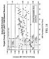
- FIG. 17shows the optical loss per centimeter, measured at 1310 nm, using a three prism coupling to the so called slab mode of the film on a 10 micron oxide, silicon wafer.
- the biased, pulsed DC film from a 60 cat. % Si and 40 cat. % Al filmdemonstrated about 0.1 dB/cm loss. After an 800° C. anneal in air, the loss was less than the measurement sensitivity of the prism coupling method.
- This dataclearly demonstrates that films deposited according to embodiments of the present invention can be used for the purpose of constructing low loss planar light wave circuits.
- Deposition of films according to the present inventioncan be utilized to deposit cladding layers, active core layers, and passive core layers of an optical amplifier structure or optical waveguide structure.
- the separation between adjacent waveguidescan be small, for example about 8 ⁇ m.
- the deposition parameters of the upper cladding layercan be adjusted to not only adjust the index of refraction of the layer, but also to insure that the spacing between adjacent waveguides is small.
- FIG. 18shows an example planarization deposition over a multiplexer structure.
- the deposition parameters from a 92 cat. % Si and 8 cat. % Alis: 5.5 Kw of Pulsed DC power applied at 200 KHz with 2.2 ⁇ s of reverse time, gas flow of 75 sccm Ar and 100 sccm O 2 , a substrate bias of 650 W (at 2 MHz), and a substrate temperature of 200° C.
- Layer 1803was deposited with an AKT 4300 based embodiment of apparatus 10 .
- the layer thickness in areas other than over waveguide structures 1801 and 1802is 11.4 ⁇ m.
- Waveguide structures 1801 and 1802are 8.20 ⁇ m high waveguides and separated by 6.09 ⁇ m at the base and by 8.40 ⁇ m at their top.
- the undercladding layer 1804is about 1.98 ⁇ m thick.
- FIG. 19illustrates deposition of material over a structure.
- Upper cladding layer 1803in region 1901 , will be angled from the horizontal by an angle ⁇ .
- the deposition and etching rates of a deposited layerdepends on the angle ⁇ .
- FIGS. 20 and 21illustrate different cases of deposition and etch rates as a function of the angle ⁇ .
- the relationship between the rate of deposition and the etch ratescan be adjusted by adjusting the deposition parameters.
- the bias power to substrate 16can be adjusted to control the relationship between the etch rates and deposition rates of material.
- FIG. 22illustrates deposition rates over a structure 2201 as a function of time.
- his the thickness deposited over structure 2201 .
- FIG. 23shows a deposited film 1803 as shown in FIG. 18 , except that the bias power to substrate 16 is set to 400 W instead of 650 W.
- a keyhole 2301is formed with an incomplete filling of uppercladding layer 1803 between structures 1801 and 1802 .
- Deposition of uppercladding layer 1803substantially follows the trends illustrated in FIGS. 19 through 22 .
- FIG. 24shows deposition as shown in FIG. 18 , except that the bias power to substrate 16 is set to 600 W instead of 650 W. As can be seen in FIG. 24 , keyhole 2301 has closed leaving a small line defect 2401 in the fill.
- FIG. 28shows deposition as shown in FIG. 18 , except that the bias power to substrate 16 is set to 900 W instead of 650 W. As can be seen in FIG. 28 , the etch rate has been increased to such an extent that the corners of structures 1801 and 1802 have been etched to form slopes 2501 and 2502 , respectively.
- an uppercladding layercan be deposited in accordance with the present invention such that it fills the space between adjacently placed waveguides.
- the parameterscan be optimized for index control and the bias power to substrate 16 can be adjusted for fill.
- other parameterse.g., the constituency of process gas, frequency and power of pulsed DC power source 14 , and other parameters in order to adjust the deposition and etch rates and thereby effectively planarize the structure as described.
- stress effects due to wafer bowing of substrate 16can also be reduced. Wafer bowing of substrate 16 can be reduced, reducing the stress in a film deposited on substrate 16 , by, for example, depositing a film on the backside of substrate 16 before deposition of a film on substrate 16 .
- a film having a similar thickness of a similar layer of materialcan be deposited on backside of substrate 16 prior to deposition of the film on substrate 16 according to the present invention. The wafer bowing resulting from differing thermal expansions of the film and substrate 16 is therefore countered by a similar stress from another film deposited on the backside of substrate 16 .
- apparatus 10utilized in the following examples was based on the AKT 1600 reactor. Further, unless otherwise specified, the temperature of substrate 16 was held at about 200° C. and the distance between substrate 16 and target 12 was 4 s/scan. The separation between substrate 16 and target 12 is about 6 cm.
- An AKT 1600 based reactorcan be utilized to deposit a film.
- a wide area metallic target of dimension 550 ⁇ 650 mm with composition (Si/Al/Er/Yb) being about 57.0 cat. % Si, 41.4 cat. % Al, 0.8 cat. % Er, and 0.8 cat. % Yb (a “0.8/0.8” target)was fabricated as described in the '247 patent.
- a 150 mm P-type silicon wafer substratewas placed in the center of a 400 ⁇ 500 mm glass carrier sheet 17 .
- Power supply 14was set to supply 6000 watts of pulse DC power at a frequency of 120 KHz with a reverse pulsing time of about 2.3 us.
- Magnet 20which is a race-track shaped magnet of approximate dimension 150 mm ⁇ 600 mm, was swept over the backside of the target at a rate of about 4 seconds per one-way scan.
- the temperature of substrate 16was held at 200C and 100 W of 2 MHz RF power was applied to substrate 16 .
- the target 12 to substrate 16 distancewas about 6.5 cm.
- the sputtering gaswas a mixture of Argon and Oxygen.
- Substrate 16 and carrier 17was preheated to 350° C. for at least 30 min prior to deposition.
- the active filmwas deposited in the poison mode. Deposition efficiency was approximately 1 um/hr.
- FIG. 5shows the hysteresis curve of this particular embodiment of target 12 .
- target 12under goes the transition from metallic to poison mode, the target voltage drops from an average of about 420V to an average of about 260V.
- step 401target 12 is cleaned by pure Argon sputtering in the metallic mode. Then target is then conditioned in poison mode with the oxygen flow much higher than the flow required at the transition region.
- Tables 1A through 1Cshows some effects on the deposited films of depositions with the 0.8/0.8 target under different operating conditions.
- Table 1Aincludes photoluminescence (pumped at 532 nm) and index of refraction for films deposited on substrate 16 with different Ar/O 2 gas flow ratios with no bias power applied to substrate 16 .
- TABLE 1ATarget Reverse Power Frequency Pulsing Bias PL/um (KW) Ar/O2 (KHz) Time (us) (W) (532 nm) Index 6 30/42 200 2.3 0 1973 1.5142 6 30/36 200 2.3 0 2358 1.5215 6 60/30 200 2.3 0 3157 1.5229 6 60/28 200 2.3 0 3421 1.5229
- Table 1Bshows the variation in photoluminescence (pumped at 532 nm) and index of refraction of the film deposited on substrate 16 with deposition processes having with the same Ar/O 2 ratios but different pulsed DC power frequencies from power supply 14 .
- TABLE 1BTarget Reverse Power Frequency Pulsing Bias PL/um (KW) Ar/O2 (KHz) Time (us) (W) (532 nm) Index 3 60/28 100 2.3 100 1472 1.5146 4 60/28 75 3.5 100 2340 1.5189 6 60/28 120 2.3 100 5178 1.5220
- Table 1Cshows the photoluinescence and index as deposited where the bias power to substrate 16 is varied.
- TABLE 1CTarget Reverse Power Frequency Pulsing Bias PL/um (KW) Ar/02 (KHz) Time (us) (W) (532 nm) Index 6 60/28 200 2.3 0 3657 1.5230 6 60/28 200 2.3 100 2187 1.5244 6 60/28 200 2.3 200 3952 1.5229 6 60/28 200 2.3 300 5000 1.5280
- the photoluminescence valuescan be measured with a Phillips PL-100.
- the deposited filmcan be pumped with a 532 nm laser and the luminescence at 980 is measured.
- the indexis the index of refraction.
- films depositedare annealed in order to activate the erbium.
- FIG. 6shows the photoluminescence and lifetime versus anneal temperature for a typical film deposited as described in this example.
- a waveguide amplifiercan be deposited according to the present invention.
- An embodiment of target 12 having composition 57.4 cat. % Si, 41.0 cat. % Al, 0.8 cat. % Er 0.8 cat. % Yb(the “0.8/0.8 target”) can be formed as disclosed in the '245 application.
- the Er—Yb (0.8/0.8) co-doped Alumino-Silicate filmwas deposited onto a 6 inch wafer of substrate 16 which includes a 10 ⁇ m thick thermal oxide substrate, which can be purchased from companies such as Silicon Quest International, Santa Clara, Calif.
- Target 12was first cleaned by sputtering with Ar (80 sccm) only in the metallic mode.
- Target 12was then conditioned in poison mode by flowing 60 sccm of Argon and 40 sccm of oxygen respectively.
- the power supplied to target 12 during conditioningwas kept at about 6 kW.
- a straight waveguide patterncan then formed by standard photolithography techniques.
- the active corewas etched using reactive ion etch followed by striping and cleaning.
- a 10 ⁇ m top cladding layeris deposited using a similar deposition process according to the present invention.
- the index difference between the top cladding layer and the active layeris about 3.7%.
- the amplifieris then annealed at 725° C. for about 30 min (see FIG. 6 , for example).
- the erbium excited-state lifetime and the up-conversion coefficientwere measured to be 3 ms and 4.5 ⁇ 10 ⁇ 18 cm 3 /s, respectively.
- a net gain of about 4 dB for small signal (about ⁇ 20 dBm) with fiber to waveguide and to fiber couplingwas obtained.
- Waveguide lengthwas 10 cm and the width was about 1.5 to 8 ⁇ m.
- the coupling loss between the fiber and the waveguideis 3-4 dB/facet, and passive excess loss is 0.1-0.2 dB/cm for 3 um waveguide.
- the waveguidewas both co- and counter pumped with 150 mW 980 nm laser per facet.
- substrate 16is a silicon substrate with an undercladding layer of thermally oxidized SiO 2 of about 15 ⁇ m thick.
- substrate 16 with the thermal oxide layercan be purchased from companies such as Silicon Quest International, Santa Clara, Calif.
- a layer of active core materialis then deposited on substrate 16 with a Shadow Mask as described in the '138 application. Use of a shadow mask results in a vertical taper on each side of a finished waveguide which greatly enhances the coupling of light into and out of the waveguide.
- Active core layeris deposited from a 0.8/0.8 target as described in the '247 application having composition 57.4 cat. % Si, 41.0 cat. % Al, 0.8 cat. % Er, and 0.8 cat. % Yb.
- the deposition parametersare identical to that of Example 2 described above.
- the active layeris deposited to a thickness of about 1.2 ⁇ m.
- a passive layer of aluminasilicateis then deposited over the active layer.
- a passive layer of about 4.25 ⁇ m thicknesscan be deposited with an embodiment of target 12 having composition of Si/Al of about 87 cat. % Si and about 13 cat. % Al.
- the passive layer and active layerare then patterned by standard lithography techniques to form a core that has a width of about 5.0 ⁇ m for the active core and tapering to about 3.5 ⁇ m at the top of the passive core with an effective length of about 9.3 cm.
- Upper cladding layeris then deposited from a Si/Al target of 92 cat. % Si and 8 cat. % Al. Deposition of the upper cladding layer is shown in FIG. 9 .
- the upper cladding layercan be deposited with a non-biased process. The thickness of the upper cladding layer can be about 10 ⁇ m.
- the amplifier formed by this processis then annealed at 725° C. for about 30 min.
- the as-deposited Erbium and Ytterbium concentrations in the active layer of core 303is 2.3 ⁇ 10 20 cm ⁇ 3 Erbium concentration and 2.3 ⁇ 10 20 cm ⁇ 3 Ytterbium concentration.
- the index of the coreis 1.508 and the index of cladding layers are 1.4458 for undercladding layer 302 and 1.452 for uppercladding layer 304 .
- the parameter ⁇ n/nis therefore about 5.0%.
- a reverse taper mode size converteris utilized for coupling light into waveguide amplifier 300 .
- the insertion loss at 1310 nmis about 2 dB.
- FIG. 26shows the amplifier performance of this example.
- amplifier 300is pumped with 150 mW from one side pumping with 984 nm light.
- Gain flatteningis achieved within about 1 dB in the range 1528 nm to 1562 nm for small input signals ( ⁇ 20 dBm). For large input signals (0 dBm), gain flattening is also achieved within about 1 dB.
- substrate 16can be a Si wafer with about a 15 ⁇ m thick thermal oxide as can be purchased from Silicon Quest International, Santa Clara, Calif.
- the embodiment of target 12 for the deposition of the active corecan have a composition of about 50 cat. % Si, 48.5 cat. % Al, 1.5 cat. % Er (the “1.5/0” target), which can be fabricated as discussed in the '138 application.
- Target 12was first cleaned by sputtering with Ar (80 sccm) only in the metallic mode.
- Target 12was then conditioned in poison mode by flowing 60 sccm of Argon and 40 sccm of oxygen respectively.
- the pulsed DC power supplied to target 12was about 6 kW. Whenever a brand new target was used or when the target has been expose to atmosphere, a long time of condition (for example more than 30 hrs of conditioning) may be necessary to ensure films with the best active core property (longest life time and highest photoluminescence) are deposited. Substrate 16 is then preheat at about 350° C. for about 30 min before deposition.
- the active core filmwas deposited onto a 6 inch thermal oxide wafer, which has been previously discussed, from the 1.5/0 target.
- the thermal oxide thicknesswas about 10 ⁇ m as described in previous examples.
- the active coreis deposited to a thickness of about 1.2 ⁇ m with a deposition time of approximately 1 hr.
- the process conditionare as listed in Table 4 below. TABLE 3 Pulsing Target Power Frequency Reverse pulsing (KW) Ar/02 (sccm) (KHz) Bias (W) time (us) 6 60/28 120 100 2.3
- a straight waveguide patterncan then be formed by a standard photolithography procedure.
- the active corewas etched using reactive ion etch followed by striping and cleaning.
- a 10 ⁇ m top cladding layeris deposited using a similar process.
- a target having composition 92 cat. % Si and 8 cat. % Al with deposition parameters as described in FIG. 9was used to deposit the top cladding. The difference between the index of refraction between the core and the cladding is then about 3.7%.
- FIG. 27shows both internal gain in the C-band and insertion loss at 1310 nm of a 2.5 ⁇ m wide, 10.1 cm long waveguide as deposited in this example as a function of annealing temperature.
- the life time in ms and up-conversion constants in cm ⁇ 3 /s measurements for the deposited active core film at different annealing temperatureare shown in FIG. 28 .
- One of the problems encountered during the reactive sputtering from an alloy metallic targetis that the film composition drifts from run to run due to the difference in sputtering yields from the elements that forms the target alloy.
- the sputtering yield of Aluminumis about 3-4 times that of Silicon, while sputtering yield of Alumina is only about 50% that of Silica. Therefore, during the metal burn in, more Aluminum is sputtered from the target, resulting in a Si rich target surface. When sputtering in the poison mode, more Silica will be removed from target.
- the composition of the film deposited on substrate 16will drift from lower Alumina concentration to higher Alumina concentration.
- FIG. 30shows the drift in photoluminescence pumped at 532 nm with subsequent depositions.
- FIG. 31shows drift in the excited state lifetime with subsequent depositions from a target.
- the embodiment of target 12 utilized in FIGS. 29 through 31is the 1.5/0 target and the deposition parameters are as described above in Example 4.
- the driftcan be stabilized by recondition target 12 prior to deposition.
- the recondition process(or burn in) consists of both sputtering in metallic mode and then sputtering in poison mode to condition target 12 .
- the burn in time in metallic modeneeds to be as short as possible and at the same time insure no arcing during the poison mode deposition.
- FIG. 32shows the much improved drift in the index of refraction and the photoluminescence when target 12 is reconditioned between subsequent depositions.
- This exampledescribes the fabrication of another Er—Yb codoped waveguide amplifier according to the present invention.
- the active coreis deposited with an embodiment of target 12 with composition about 49 cat. % Si, 48 cat. % Al, 1.6 cat. % Er and 0.5 cat. % Yb, which can be fabricated as described in the '247 application.
- Target 12was first cleaned by sputtering with Ar (80 sccm) only in the metallic mode.
- Target 12was then conditioned in poison mode by flowing 60 sccm of Argon and 40 sccm of oxygen respectively.
- the pulsed DC power supplied to target 12was kept at 5 kW.
- Table 4shows photoluminescence and index of refraction of as-deposited films from this example at some typical process conditions.
- the units for photoluminescenceare the number of counts per micron. Lifetime and photoluminescence measured after annealing at various different temperatures are shown in Table 5.
- Target 4Target Pulsing Reverse Power Ar/O2 Frequency Bias pulsing time 532 nm (KW) (sccm) (KHz) (W) (us) PL/um Index 5 60/34 120 100 2.3 3367 1.5333 5 60/30 120 100 2.3 3719 1.5334
- a waveguide amplifierwas fabricated using this material in the similar fashion as described in examples 2-4.
- the active corewas first deposited on substrate 16 , which includes a 10 um thermal oxide layer, using the following deposition parameters: target power 5 KW, pulsing frequency 120 KHz, bias 100 W, reverse time 2.3 us, Argon and Oxygen flow are 60 sccm and 30 sccm respectively.
- the active core thicknessis deposited to a thickness about 1.2 ⁇ m, which takes approximately 1 hr. All wafers are preheated at about 350° C. for 30 min before deposition.
- a straight waveguide patternis then formed by standard photolithography procedure.
- the active corewas etched using reactive ion etch following by striping and cleaning.
- top cladding layeris deposited using similar process.
- the “92/8” (92 cat. % Si and 8 cat. % Al) metallic targetwas used to deposit top clad according to deposition parameters shown in FIG. 9 , resulting in a 4% index difference between active core and cladding.
- the wave guidewas then annealed at 800° C. for about 30 min.
- This waveguidewas tested for gain using the method described in previous examples. However no net gain was observed from this waveguide since the passive loss was too high.
- passive layerscan also be deposited.
- FIG. 9shows deposition parameters for several target compositions, including some targets for deposition of passive (i.e., alloys of Al and Si with no rare earth ion concentration) layers.
- target 12 with a material composition of pure siliconis utilized.
- Apparatus 10can be based on an AKT 1600 reactor and deposited with about 1 to 3 kW of pulsed DC target power supplied to target 12 . Particular depositions have been accomplished at 2.5 kW and 1.5 kW.
- the frequency of the pulsed DC poweris between about 100 and 200 Khz. Some depositions were performed at 200 kHz while others were performed at 100 kHz.
- the reverse timewas varied between about 2 ⁇ s and about 4 ⁇ s with particular depositions performed at 2.3 ⁇ s and 3.5 ⁇ s.
- the bias power to substrate 16was set to zero.
- the process gasincluded a mixture of Ar, N 2 and O 2 .
- the Ar flow rateswas set at 20 sccm while the O 2 flow rate was varied between about 5 and about 20 sccm and the N 2 flow rate was varied from about 2 to about 35 sccm.
- FIG. 33shows the variation in the index of refraction of a film deposition on substrate 16 as the O 2 /N 2 ratio is varied.
- filmscan be deposited on substrate 16 from a pure alumina target.
- the pulsed DC target powerwas set at 3 kW and the frequency was varied between about 60 kHz and 200 kHz.
- the reverse timewas set at 2.5 ⁇ s. Again, no bias power was supplied to substrate 16 .
- the O 2 flow ratewas varied from about 20 to about 35 sccm, with particular depositions performed at 22 and 35 sccm.
- the Ar flow ratewas set at 26 sccm.
- a post deposition anneal of substrate 16 at 800° C. for 30 min.was performed.
- FIG. 12shows the variation of refractive index of the film deposited on substrate 16 with varying frequency of the pulsed DC power supplied to target 12 .
- FIG. 11shows the variation in refractive index of a film deposited on substrate 16 with varying O 2 /Ar ratio.
- the index of refraction of films deposited from aluminacan be adjusted by adjusting the process gas constituents or by adjusting the frequency of the pulsed DC power supplied to target 12 during deposition.
- passive filmscan be deposited from targets having a composition of Si and Al.
- targets having a composition of Si and AlFor example, layers have been deposited from embodiments of target 12 with composition 83% Si and 17% Al.
- About 4.5 kW of pulsed DC power at about 200 kHz frequencywas supplied to target 12 .
- the reverse timewas about 2.2 ⁇ s.
- a bias power of about 150 Wwas supplied to substrate 16 during deposition.
- FIGS. 14 and 15show variation of the index of refraction for subsequent runs from this target.
Landscapes
- Chemical & Material Sciences (AREA)
- Engineering & Computer Science (AREA)
- Organic Chemistry (AREA)
- Materials Engineering (AREA)
- Mechanical Engineering (AREA)
- Metallurgy (AREA)
- Chemical Kinetics & Catalysis (AREA)
- Physics & Mathematics (AREA)
- Plasma & Fusion (AREA)
- Analytical Chemistry (AREA)
- Thermal Sciences (AREA)
- Microelectronics & Electronic Packaging (AREA)
- General Physics & Mathematics (AREA)
- Optics & Photonics (AREA)
- Physical Vapour Deposition (AREA)
Abstract
Description
- 1. Field of the Invention
- The present invention relates to deposition of oxide and oxynitride films and, in particular, to deposition of oxide and oxynitride films by pulsed DC reactive sputtering.
- 2. Discussion of Related Art
- Deposition of insulating materials and especially optical materials is technologically important in several areas including production of optical devices and production of semiconductor devices. In semiconductor devices, doped alumina silicates can be utilized as high dielectric insulators.
- The increasing prevalence of fiber optic communications systems has created an unprecedented demand for devices for processing optical signals. Planar devices such as optical waveguides, couplers, splitters, and amplifiers, fabricated on planar substrates, like those commonly used for integrated circuits, and configured to receive and process signals from optical fibers are highly desirable. Such devices hold promise for integrated optical and electronic signal processing on a single semiconductor-like substance.
- The basic design of planar optical waveguides and amplifiers is well known, as described, for example, in U.S. Pat. No. 5,119,460 and U.S. Pat. No. 5,563,979 to Bruce et al., U.S. Pat. No. 5,613,995 to Bhandarkar et al., U.S. Pat. No. 5,900,057 to Buchal et al., and U.S. Pat. No. 5,107,538 to Benton et al., to cite only a few. These devices, very generally, include a core region, typically bar shaped, of a certain refractive index surrounded by a cladding region of a lower refractive index. In the case of an optical amplifier, the core region includes a certain concentration of a dopant, typically a rare earth ion such as an erbium or praseodymium ion which, when pumped by a laser, fluoresces, for example, in the 1550 nm and 1300 nm wavelength ranges used for optical communication, to amplify the optical signal passing through the core.
- As described, for example in the patents by Bruce et al., Bhandarkar et al, and Buchal et al., planar optical devices may be fabricated by process sequences including forming a layer of cladding material on a substrate; forming a layer of core material on the layer of cladding mater; patterning the core layer using a photolighotgraphic mask and an etching process to form a core ridge; and covering the core ridge with an upper cladding layer.
- The performance of these planar optical devices depends sensitively on the value and uniformity of the refractive index of the core region and of the cladding region, and particularly on the difference in refractive index, Δn, between the regions. Particularly for passive devices such as waveguides, couplers, and splitters, Δn should be carefully controlled, for example to values within about 1%, and the refractive index of both core and cladding need to be highly uniform, for some applications at the fewer than parts per thousand level. In the case of doped materials forming the core region of planar optical amplifiers, it is important that the dopant be uniformly distributed so as to avoid non-radiative quenching or radiative quenching, for example by upconversion. The refractive index and other desirable properties of the core and cladding regions, such as physical and chemical uniformity, low stress, and high density, depend, of course, on the choice of materials for the devices and on the processes by which they are fabricated.
- Because of their optical properties, silica and refractory oxides such as Al2O3, are good candidate materials for planar optical devices. Further, these oxides serve as suitable hosts for rare earth dopants used in optical amplifiers. A common material choice is so-called low temperature glasses, doped with alkali metals, boron, or phosphorous, which have the advantage of requiring lower processing temperatures. In addition, dopants are used to modify the refractive index. Methods such as flame hydrolysis, ion exchange for introducing alkali ions in glasses, sputtering, and various chemical vapor deposition processes (CVD) have been used to form films of doped glasses. However, dopants such as phosphorous and boron are hygroscopic, and alkalis are undesirable for integration with electronic devices. Control of uniformity of doping in CVD processes can be difficult and CVD deposited films can have structural defects leading to scattering losses when used to guide light. In addition, doped low temperature glasses may require further processing after deposition. A method for eliminating bubbles in thin films of sodium-boro-silicate glass by high temperature sintering is described, for example, in the '995 patent to Bhandarkar et al.
- Typically, RF sputtering has been utilized for deposition of oxide dielectric films. However, RF sputtering utilizes ceramic targets which are typically formed of multiple smaller tiles. Since the tiles can not be made very large, there may be a large problem of arcing between tiles and therefore contamination of the deposited film due to this arcing. Further, the reactors required for RF sputtering tend to be rather complicated. In particular, the engineering of low capacitance efficient RF power distribution to the cathode is difficult in RF systems. Routing of low capacitance forward and return power into a vacuum vessel of the reaction chamber often exposes the power path in such a way that diffuse plasma discharge is allowed under some conditions of impedance tuning of the matching networks.
- Therefore, there is a need for new methods of depositing oxide and oxynitride films and for forming planar optical devices.
- In accordance with the present invention, a sputtering reactor apparatus for depositing oxide and oxynitride films is presented. Further, methods for depositing oxide and oxynitride films for optical waveguide devices are also presented. A sputtering reactor according to the present invention includes a pulsed DC power supply coupled through a filter to a target and a substrate electrode coupled to an RF power supply. A substrate mounted on the substrate electrode is therefore supplied with a bias from the RF power supply.
- The target can be a metallic target made of a material to be deposited on the substrate. In some embodiments, the metallic target is formed from Al, Si and various rare-earth ions. A target with an erbium concentration, for example, can be utilized to deposit a film that can be formed into a waveguide optical amplifier.
- A substrate can be any material and, in some embodiments, is a silicon wafer. In some embodiments, RF power can be supplied to the wafer. In some embodiments, the wafer and the electrode can be separated by an insulating glass.
- In some embodiments, up to about 10 kW of pulsed DC power at a frequency of between about 40 kHz and 350 kHz and a reverse pulse time of up to about 5 μs is supplied to the target. The wafer can be biased with up to about several hundred watts of RF power. The temperature of the substrate can be controlled to within about 10° C. and can vary from about −50° C. to several hundred degrees C. Process gasses can be fed into the reaction chamber of the reactor apparatus. In some embodiments, the process gasses can include combinations of Ar, N2, O2, C2F6, CO2, CO and other process gasses.
- Several material properties of the deposited layer can be modified by adjusting the composition of the target, the composition and flow rate of the process gasses, the power supplied to the target and the substrate, and the temperature of the substrate. For example, the index of refraction of the deposited layer depends on deposition parameters. Further, in some embodiments stress can be relieved on the substrate by depositing a thin film of material on a back side of the wafer. Films deposited according to the present invention can be utilized to form optical waveguide devices such as multiplexers and rare-earth doped amplifiers.
- These and other embodiments, along with examples of material layers deposited according to the present invention, are further described below with respect to the following figures.
FIGS. 1A and 1B show a pulsed DC sputtering reactor according to the present invention.FIG. 2 shows a planar view of target utilized in a reactor as shown inFIGS. 1A and 1B .FIG. 3 shows a cross-section view of an example target utilized in a reactor as shown inFIGS. 1A and 1B .FIG. 4 shows a flow chart of an embodiment of a process for depositing a film on a substrate according to the present invention.FIG. 5 shows a hysterises curve of target voltage versus oxygen flow rates for an example target in an embodiment of a reactor according to the present invention.FIG. 6 shows a photo-luminescence and lifetimes of a film deposited in a process according to the present invention as a function of after deposition anneal temperature.FIG. 7 shows the relationship between the index of refraction of a film as a function of deposited oxide layers according to the present invention and due to oxide build-up on the target.FIG. 8 shows a graph of the index of refraction of a film deposited according to the present invention as a function of the aluminum content in a composite Al/Si target.FIG. 9 shows a graph of typical indices of refraction of material layers deposited according to the present invention.FIG. 10 shows a table of indices of refraction for a silica layer deposited according to the present invention as a function of different process parameters.FIG. 11 shows the refractive indices as a function of O2/Ar ratio utilized in an Alumina process according to the present invention.FIG. 12 shows the refractive indices as a function of DC pulsed power frequency for an Alumina layer deposited according to the present invention.FIG. 13 shows variation in the refractive index over time during repeated depositions from a single target.FIG. 14 shows variation in refractive index over time for repeated depositions from a target of another material layer according to the present invention.FIG. 15 shows the variation refractive index over time for repeated depositions from a target of another material layer according to the present invention.FIG. 16A through 16D shows a TEM film deposited according to the present invention.FIG. 17 shows the transparency of a film deposited according to the present invention.FIG. 18 shows an uppercladding layer deposited according to the present invention over a multiple-waveguide structure such that the deposited layer is substantially planarized.FIG. 19 illustrates the deposition of a film over a waveguide structure.FIGS. 20 and 21 illustrate different etch and deposition rates for deposition of films as a function of the surface angle of the film.FIG. 22 illustrates calculation of the planarization time for a particular deposition process.FIGS. 23 through 25 through illustrate adjustment of process parameters in order to achieve planarization of a film deposited over a waveguide structure according to the present invention.FIG. 26 shows the gain characteristics of an erbium doped waveguide amplifier formed of films depositions according to the present invention.FIG. 27 shows gain, insertion loss of a waveguide with an active core deposited according to the present invention.FIG. 28 shows up-conversion constants, and lifetimes of the active core layer ofFIG. 27 deposited according to the present invention.FIG. 29 shows drift in the index of refraction with subsequent depositions for films deposited from a target according to the present invention.FIG. 30 shows drift in the photoluminescence with subsequent depositions according to the present invention.FIG. 31 shows drift in the excited state lifetime with subsequent depositions according to the present invention.FIG. 32 shows stabilization of the index of refraction in subsequent depositions.FIG. 33 shows the index of refraction of a film formed from a pure silicon target as a function of the ratio of O2/N2in the process gas.- In the figures, elements having the same designation have the same or similar function.
- Reactive DC magnetron sputtering of nitrides and carbides is a widely practiced technique, but the reactive dc magnetron sputtering of nonconducting oxides is done rarely. Films such as aluminum oxide are almost impossible to deposit by conventional reactive DC magnetron sputtering due to rapid formation of insulating oxide layers on the target surface. The insulating surfaces charges up and result in arcing during process. This arcing can damage the power supply, produce particles and degrade the properties of deposited oxide films.
- RF sputtering of oxide films is discussed in application Ser. No. 09/903,050 (the '050 application) by Demaray et al., entitled “Planar Optical Devices and Methods for Their Manufacture,” assigned to the same assignee as is the present invention, herein incorporated by reference in its entirety. Further, targets that can be utilized in a reactor according to the present invention are discussed in U.S. application Ser. No. {Attorney Docket No. M-12247 US} (the '247 application), filed concurrently with the present disclosure, assigned to the same assignee as is the present invention, herein incorporated by reference in its entirety. A gain-flattened amplifier formed of films deposited according to the present invention are described in U.S. application Ser. No. {Attorney Docket No. M-12652 US} (the '652 application), filed concurrently with the present disclosure, assigned to the same assignee as is the present invention, herein incorporated by reference in its entirety. Further, a mode size converter formed with films deposited according to the present invention is described in U.S. application Ser. No. {Attorney Docket No. M-12138 US} (the '138 application), filed concurrently with the present disclosure, assigned to the same assignee as is the present invention, herein incorporated by reference in its entirety.
FIG. 1A shows a schematic of areactor apparatus 10 for sputtering of material from atarget 12 according to the present invention. In some embodiments,apparatus 10 may, for example, be adapted from an AKT-1600 PVD (400×500 mm substrate size) system from Applied Komatsu or an AKT-4300 (600×720 mm substrate size) system from Applied Komatsu, Santa Clara, Calif. The AKT-1600 reactor, for example, has three deposition chambers connected by a vacuum transport chamber. These Komatsu reactors can be modified such that pulsed DC power is supplied to the target and RF power is supplied to the substrate during deposition of a material film.Apparatus 10 includes atarget 12 which is electrically coupled through afilter 15 to a pulsedDC power supply 14. In some embodiments,target 12 is a wide area sputter source target, which provides material to be deposited onsubstrate 16.Substrate 16 is positioned parallel to andopposite target 12.Target 12 functions as a cathode when power is applied to it and is equivalently termed a cathode. Application of power to target12 creates aplasma 53.Substrate 16 is capacitively coupled to anelectrode 17 through aninsulator 54.Electrode 17 can be coupled to anRF power supply 18.Magnet 20 is scanned across the top oftarget 12.- For pulsed reactive dc magnetron sputtering, as performed by
apparatus 10, the polarity of the power supplied to target12 bypower supply 14 oscillates between negative and positive potentials. During the positive period, the insulating layer on the surface oftarget 12 is discharged and arcing is prevented. To obtain arc free deposition, the pulsing frequency exceeds a critical frequency that depend on target material, cathode current and reverse time. High quality oxide films can be made using reactive pulse DC magnetron sputtering inapparatus 10. - Pulsed
DC power supply 14 can be any pulsed DC power supply, for example an AE Pinnacle plus 10K by Advanced Energy, Inc. With this example supply, up to 10 kW of pulsed DC power can be supplied at a frequency of between 0 and 350 KHz. The reverse voltage is 10% of the negative target voltage. Utilization of other power supplies will lead to different power characteristics, frequency characteristics and reverse voltage percentages. The reverse time on this embodiment ofpower supply 14 can be adjusted between 0 and 5 μs. Filter 15 prevents the bias power frompower supply 18 from coupling into pulsedDC power supply 14. In some embodiments,power supply 18 is a 2 MHz RF power supply, for example can be a Nova-25 power supply made by ENI, Colorado Springs, Co.- Therefore, filter15 is a 2 MHz band rejection filter. In some embodiments, the band width of the filter can be approximately 100 kHz.
Filter 15, therefore, prevents the 2 MHz power from the bias tosubstrate 16 fromdamaging power supply 18. - However, both RF and pulsed DC deposited films are not fully dense and most likely have columnar structures. These columnar structures are detrimental for optical wave guide applications due to the scattering loss caused by the structure. By applying a RF bias on
wafer 16 during deposition, the deposited film can be dandified by energetic ion bombardment and the columnar structure can be substantially eliminated. - In the AKT-1600 based system, for example, target12 can have an active size of about 675.70×582.48 by 4 mm in order to deposit films on
substrate 16 that have dimension about 400×500 mm. The temperature ofsubstrate 16 can be held at between −50C and 500C. The distance betweentarget 12 andsubstrate 16 can be between about 3 and about 9 cm. Process gas can be inserted into the chamber ofapparatus 10 at a rate up to about 200 sccm while the pressure in the chamber ofapparatus 10 can be held at between about 0.7 and 6 millitorr.Magnet 20 provides a magnetic field of strength between about 400 and about 600 Gauss directed in the plane oftarget 12 and is moved acrosstarget 12 at a rate of less than about 20-30 sec/scan. In some embodiments utilizing theAKT 1600 reactor,magnet 20 can be a race-track shaped magnet with dimension about 150 mm by 600 mm. - A top down view of
magnet 20 andwide area target 12 is shown inFIG. 2 . A film deposited on a substrate positioned oncarrier sheet 17 directly opposed toregion 52 oftarget 12 has good thickness uniformity.Region 52 is the region shown inFIG. 1B that is exposed to a uniform plasma condition. In some implementations,carrier 17 can be coextensive withregion 52.Region 24 shown inFIG. 2 indicates the area below which both physically and chemically uniform deposition can be achieved, where physical and chemical uniformity provide refractive index uniformity, for example.FIG. 2 indicates thatregion 52 oftarget 12 that provides thickness uniformity is, in general, larger thanregion 24 oftarget 12 providing thickness and chemical uniformity. In optimized processes, however,regions - In some embodiments,
magnet 20 extends beyondarea 52 in one direction, the Y direction inFIG. 2 , so that scanning is necessary in only one direction, the X direction, to provide a time averaged uniform magnetic field. As shown inFIGS. 1A and 1B ,magnet 20 can be scanned over the entire extent oftarget 12, which is larger thanregion 52 of uniform sputter erosion.Magnet 20 is moved in a plane parallel to the plane oftarget 12. - The combination of a
uniform target 12 with atarget area 52 larger than the area ofsubstrate 16 can provide films of highly uniform thickness. Further, the material properties of the film deposited can be highly uniform. The conditions of sputtering at the target surface, such as the uniformity of erosion, the average temperature of the plasma at the target surface and the equilibration of the target surface with the gas phase ambient of the process are uniform over a region which is greater than or equal to the region to be coated with a uniform film thickness. In addition, the region of uniform film thickness is greater than or equal to the region of the film which is to have highly uniform optical properties such as index of refraction, density, transmission or absorptivity. Target 12 can be formed of any materials, but is typically metallic materials such as, for example, combinations of Al and Si. Therefore, in some embodiments,target 12 includes a metallic target material formed from intermetalic compounds of optical elements such as Si, Al, Er and Yb. Additionally, target12 can be formed, for example, from materials such as La, Yt, Ag, Au, and Eu. To form optically active films onsubstrate 16,target 12 can include rare-earth ions. In some embodiments oftarget 12 with rare earth ions, the rare earth ions can be pre-alloyed with the metallic host components to form intermetalics. See the '247 application.- In several embodiments of the invention, material tiles are formed. These tiles can be mounted on a backing plate to form a target for
apparatus 10.FIG. 3A shows an embodiment oftarget 12 formed withindividual tiles 30 mounted on a cooledbackplate 25. In order to form a wide area target of an alloy target material, the consolidated material ofindividual tiles 30 should first be uniform to the grain size of the powder from which it is formed. It also should be formed into a structural material capable of forming and finishing to a tile shape having a surface roughness on the order of the powder size from which it is consolidated. A wide area sputter cathode target can be formed from a close packed array of smaller tiles.Target 12, therefore, may include any number oftiles 30, for example between 2 to 20individual tiles 30.Tiles 30 are finished to a size so as to provide a margin of non-contact, tile to tile,29 inFIG. 3A , less than about 0.010″ to about 0.020″ or less than half a millimeter so as to eliminate plasma processes between adjacent ones oftiles 30. The distance betweentiles 30 oftarget 12 and the dark space anode orground shield 19, inFIG. 1B can be somewhat larger so as to provide non contact assembly or provide for thermal expansion tolerance during process chamber conditioning or operation. - Several useful examples of
target 12 that can be utilized inapparatus 10 according to the present invention include the following targets compositions: (Si/Al/Er/Yb) being about (57.0/41.4/0.8/0.8), (48.9/49/1.6/0.5), (92/8/0/0), (60/40/0/0), (50/50/0/0), (65/35/0/0), (70/30/0,0), and (50,48.5/1.5/0) cat. %, to list only a few. These targets can be referred to as the 0.8/0.8 target, the 1.6/0.5 target, the 92-8 target, the 60-40 target, the 50-50 target, the 65-35 target, the 70-30 target, and the 1.5/0 target, respectively. The 0.8/0.8, 1.6/0.5, and 1.5/0 targets can be made by pre-alloyed targets formed from an atomization and hot-isostatic pressing (HIPing) process as described in the '247 application. The remaining targets can be formed, for example, by HIPing. Targets formed from Si, Al, Er and Yb can have any composition. In some embodiments, the rare earth content can be up to 10 cat. % of the total ion content in the target. Rare earth ions are added to form active layers for amplification. Targets utilized inapparatus 10 can have any composition and can include ions other than Si, Al, Er and Yb, including: Zn, Ga, Ge, P, As, Sn, Sb, Pb, Ag, Au, and rare earths: Ce, Pr, Nd, Pm, Sm, Eu, Gd, Th, Dy Ho, Er, Tm Yb and Lu. - Optically useful materials to be deposited onto
substrate 16 include oxides, fluorides, sulfides, nitrides, phosphates, sulfates, and carbonates, as well as other wide band gap semiconductor materials. To achieve uniform deposition,target 12, itself can be chemically uniform and of uniform thickness over an extended area. Target 12 can be a composite target fabricated from individual tiles, precisely bonded together on a backing plate with minimal separation, as is discussed further with respect toFIG. 3 . In some embodiments, the mixed intermetalllics can be plasma sprayed directly onto a backing plate to formtarget 12. The complete target assembly can also includes structures for cooling the target, embodiments of which have been described in U.S. Pat. No. 5,565,071 to Demaray et al, and incorporated herein by reference.Substrate 16 can be a solid, smooth surface. Typically,substrate 16 can be a silicon wafer or a silicon wafer coated with a layer of silicon oxide formed by a chemical vapor deposition process or by a thermal oxidation process. Alternatively,substrate 16 can be a glass, such as Corning 1737 (Corning Inc., Elmira, N.Y.), a glass-like material, quartz, a metal, a metal oxide, or a plastic material.Substrate 16 can be supported on a holder or carrier sheet that may be larger thansubstrate 16.Substrate 16 can be electrically biased bypower supply 18.- In some embodiments, the area of
wide area target 12 can be greater than the area on the carrier sheet on which physically and chemically uniform deposition is accomplished. Secondly, in some embodiments a central region ontarget 12, overlyingsubstrate 16, can be provided with a very uniform condition of sputter erosion of the target material. Uniform target erosion is a consequence of a uniform plasma condition. In the following discussion, all mention of uniform condition of target erosion is taken to be equivalent to uniform plasma condition. Uniform target erosion is evidenced by the persistence of film uniformity throughout an extended target life. A uniformly deposited film can be defined as a film having a nonuniformity in thickness, when measured at representative points on the entire surface of a substrate wafer, of less than about 5% or 10%. Thickness nonuniformity is defined, by convention, as the difference between the minimum and maximum thickness divided by twice the average thickness. If films deposited from a target from which more than about 20% of the weight of the target has been removed continue to exhibit thickness uniformity, then the sputtering process is judged to be in a condition of uniform target erosion for all films deposited during the target life. - As shown in
FIG. 1B , a uniform plasma condition can be created in the region betweentarget 12 andsubstrate 16 in aregion overlying substrate 16. Aplasma 53 can be created in region51, which extends under theentire target 12. Acentral region 52 oftarget 12, can experience a condition of uniform sputter erosion. As discussed further below, a layer deposited on a substrate placed anywhere belowcentral region 52 can then be uniform in thickness and other properties (i.e., dielectric, optical index, or material concentrations). - In addition,
region 52 in which deposition provides uniformity of deposited film can be larger than the area in which the deposition provides a film with uniform physical or optical properties such as chemical composition or index of refraction. In some embodiments,target 12 is substantially planar in order to provide uniformity in the film deposited onsubstrate 16. In practice, planarity oftarget 12 can mean that all portions of the target surface inregion 52 are within a few millimeters of a planar surface, and can be typically within 0.5 mm of a planar surface. - Other approaches to providing a uniform condition of sputter erosion rely on creating a large uniform magnetic field or a scanning magnetic field that produces a time-averaged, uniform magnetic field. For example, rotating magnets or electromagnets can be utilized to provide wide areas of substantially uniform target erosion. For magnetically enhanced sputter deposition, a scanning magnet magnetron source can be used to provide a uniform, wide area condition of target erosion.
- As illustrated in
FIG. 1A ,apparatus 10 can include a scanningmagnet magnetron source 20 positioned abovetarget 12. An embodiment of a scanning magnetron source used for dc sputtering of metallic films is described in U.S. Pat. No. 5,855,744 to Halsey, et. al., (hereafter '744), which is incorporated herein by reference in its entirety. The '744 patent demonstrates the improvement in thickness uniformity that is achieved by reducing local target erosion due to magnetic effects in the sputtering of a wide area rectangular target. As described in the '744 patent, by reducing the magnetic field intensity at these positions, the local target erosion was decreased and the resulting film thickness nonuniformity was improved from 8%, to 4%, over a rectangular substrate of 400×500 mm. - The process gas utilized in
reactor 10 includes an inert gas, typically argon, used as the background sputtering gas. Additionally, with some embodiments oftarget 12, reactive components such as, for example, oxygen may be added to the sputtering gas. Other gasses such as N2, NH3, CO, NO, CO2, halide containing gasses other gas-phase reactants can also be utilized. The deposition chamber can be operated at low pressure, often between about 0.5 millitorr and 8-10 millitorr. Typical process pressure is below about 3-5 millitorr where there are very few collisions in the gas phase, resulting in a condition of uniform “free molecular” flow. This ensures that the gas phase concentration of a gaseous component is uniform throughout the process chamber. For example, background gas flow rates in the range of up to about 200 sccm, used with a pump operated at a fixed pumping speed of about 50 liters/second, result in free molecular flow conditions. - The distance d, in
FIG. 1A , betweentarget 12 andsubstrate 16 can, in some embodiments, be varied between about 4 cm and about 9 cm. A typical target to substrate distance d is about 6 cm. The target to substrate distance can be chosen to optimize the thickness uniformity of the film. At large source to substrate distances the film thickness distribution is dome shaped with the thickest region of the film at the center of the substrate. At close source to substrate distance the film thickness is dish shaped with the thickest film formed at the edge of the substrate. The substrate temperature can be held constant in the range of about −40° C. to about 550° C. and can be maintained at a chosen temperature to within about 10° C. by means of preheatingsubstrate 16 and the substrate holder prior to deposition. During the course of deposition, the heat energy impressed upon the substrate by the process can be conducted away fromsubstrate 16 by cooling the table on whichsubstrate 16 is positioned during the process, as known to those skilled in the art. The process is performed under conditions of uniform gas introduction, uniform pumping speed, and uniform application of power to the periphery of the target as known to skilled practitioners. - The speed at which a
scanning magnet 20 can be swept over the entire target can be determined such that a layer thickness less than about 5 to 10 Å, corresponding roughly to two to four monolayers of material, is deposited on each scan.Magnet 20 can be moved at rates up to about 30 sec/one-way scan and typically is moved at a rate of about 4 sec/one-way scan. The rate at which material is deposited depends on the applied power and on the distance d, inFIG. 1A , between thetarget 12 and thesubstrate 16. For deposition of optical oxide materials, for example scanning speeds between about 2 sec/one-way scan across the target to 20-30 sec/scan provide a beneficial layer thickness. Limiting the amount of material deposited in each pass promotes chemical and physical uniformity of the deposited layer. - Substrate bias has been used previously to planarize RF sputtered deposited quartz films. A theoretical model of the mechanism by which substrate bias operates, has been put forward by Ting et al. (J. Vac. Sci. Technol. 15, 1105 (1978)). When power is applied to the substrate, a so-called plasma sheath is formed about the substrate and ions are coupled from the plasma. The sheath serves to accelerate ions from the plasma so that they bombard the film as it is deposited, sputtering the film, and forward scattering surface atoms, densifying the film and eliminating columnar structure. The effects of adding substrate bias are akin to, but more dramatic than, the effects of adding the low frequency RF component to the sputter source.
Biasing substrate 16 results in the deposited film being simultaneously deposited and etched. The net accumulation of film at any point on a surface depends on the relative rates of deposition and etching, which depend respectively, on the power applied to the target and to the substrate, and to the angle that the surface makes with the horizontal. The rate of etching is greatest for intermediate angles, on the order of 45 degrees, that is between about 30 and 60 degrees.- Powers to target12 and
substrate 16 can be adjusted such that the rates of deposition and etching are approximately the same for a range of intermediate angles. In this case, films deposited with bias sputtering have the following characteristics. At a step where a horizontal surface meets a vertical surface, the deposited film makes an intermediate angle with the horizontal. On a surface at an intermediate angle, there will be no net deposition since the deposition rate and etch rate are approximately equal. There is net deposition on a vertical surface. Target 12 can have an active size of about 675.70×582.48 by 4 mm, for example, in a AKT-1600 based system in order to deposit films on asubstrate 16 that is about 400×500 mm. The temperature ofsubstrate 16 can be held at between −50C and 500C. The distance betweentarget 12 andsubstrate 16 can be between 3 and 9 cm. Process gas can be inserted into the chamber ofapparatus 10 at a rate of between about 30 to about 100 sccm while the pressure in the chamber ofapparatus 10 can be held at below about 2 millitorr.Magnet 20 provides a magnetic field of strength between about 400 and about 600 Gauss directed in the plane oftarget 12 and is moved acrosstarget 12 at a rate of less than about 20-30 sec/scan.- Therefore, any given
process utilizing apparatus 10 can be characterized by providing the power supplied to target12, the power supplied tosubstrate 16, the temperature ofsubstrate 16, the characteristics and constituents of the reactive gasses, the speed of the magnet, and the spacing betweensubstrate 16 andtarget 12. - Sputtered oxide films according to some embodiments of the present invention can be deposited onto a Si wafer or thermal oxide wafers at pressure of between about 3 and about 6 mTorr. The ratio of O2/Ar gas flow can be set at a value to ensure that
target 12 is operating within a poison mode. The poison mode is defined as the ratio where the oxide is etched from the surface oftarget 12 as fast as the oxide layer is formed. Operating in the poison mode results in the stoichiometric film. Sub-stoichiometric oxides may not be optically transparent. The pulsing frequency range forpower supply 14 can be from about up to about 250 KHz. Thefrequency 40 KHz is approximately the lowest frequency at which no arcing will occur during deposition in, for example, theAKT 1600 based system. The reverse pulsing time is determined by the amount of arcing generated during the process. Longer reverse time means longer discharge time and thus less arcs. However, if the reverse time is too long, the deposition rate will decrease.Power supply 18 is a 2 MHz RF power supply operated at powers up to several hundred Watts. FIG. 4 shows an embodiment of aprocess procedure 400 performed onapparatus 10. Instep 401, the target is prepared for the deposition. In some embodiments, target12 can be cleaned by pure Ar sputtering. In other words,apparatus 10 is operated with pure Ar gas only (referred to as the metal mode) in order to sputter away a surface layer oftarget 12.FIG. 7 shows the typical drift in the index of refraction with deposition of oxide layers for several different targets over different runs for each target. InFIG. 7 , the compositions of the target materials utilized intarget 12 for the depositions shown are as follows: Si: 60 cat. % and Al: 40 cat. %; Si: 50 cat. % and Al: 50 cat. %; Si: 85 cat. % and Al: 15 cat. %; Si: 35 cat. % and Al: 65 cat. %; and Si: 92 cat. % and 8 cat. %. Each deposition was operated under the same process parameters: 4.5 kW of pulsed DC power at 200 kHz with a reverse time of 2.3 μs applied to target12, O2flow at 44 sccm, Ar flow at 30 sccm introduced toapparatus 10, 100 W of bias power at 2 MHz applied tosubstrate 16, the temperature ofsubstrate 16 held at 200° C., and the distance betweensubstrate 16 andtarget 12 being set at 6 cm. For each target measured, the index drifted up during repeated utilization.FIG. 8 shows the relationship between the index of refraction of a film deposited according to the present invention and the amount of aluminum in the composite target. As can be seen fromFIG. 8 , the index of refraction of the deposited film depends strongly on the aluminum content. Therefore, as the aluminum in a metal target is depleted, the index of refraction drifts. In some embodiments, the ratio of Ar and O2utilized in the process can be maintained to provide films of uniform index over a large number of depositions on the target.- Reactive sputtering from a metal or
metallic alloy target 12 can be characterized by two modes of operation. In the first mode, which is sometimes referred to as the ‘metallic mode’ the surface oftarget 12 is substantially metallic. This mode is characterized by a small addition of reactive gas to the inert gas flow ofapparatus 10 as well as a higher impedance magnetron discharge. It is also characterized by incomplete oxidation of film deposited onsubstrate 16 and therefore higher index films. As the proportion of reactive to inert gas is increased, the sputter voltage attarget 12 begins to fall at constant power. FIG. 5 shows the voltage ontarget 12 of an embodiment ofapparatus 10 according to the present invention as a function of process gas constitution. In the example illustrated inFIG. 5 , for example, a metallic target with composition 0.8 cat. % Er, 0.8 cat. % Yb, 57.4 cat. % Si and 41 cat. % Si, which can be formed as described in the '247 application, was sputtered in an embodiment ofapparatus 10 based on the AKT-1600 PVD system with 6 kW of pulsed DC power at a frequency of 120 kHz and a reverse time of 2.3 micro seconds. The Argon gas flow was set at 60 sccm and the Oxygen gas flow was varied from zero up to 40 sccm. For more details regarding this deposition, see Example 1 below.- As shown in
FIG. 5 , the voltage ontarget 12 during deposition (the “target voltage”) was constant at about 420 Volts for oxygen flow rates up to about 20 sccm. This is clearly the metallic mode of operation for this embodiment oftarget 12. Films deposited in this range of oxygen flow are characterized as metallic with an oxygen content that increases with oxygen flow rate during deposition. As the oxygen flow is increased up to about 26 sccm, the voltage ontarget 12 begins to decrease, indicating that the surface oftarget 12 is beginning to form an oxide layer. The oxide layer on the surface oftarget 12 has a higher secondary electron yield under the influence of the Argon ion flux. The additional electron flux to the magnetron electron trap increases the ion production in the plasma, which, in turn, decreases the impedance of the plasma discharge inapparatus 10. - At slightly higher oxygen flow during deposition, the oxide layer on
target 12 forms a continuous layer and the voltage oftarget 12 during deposition falls rapidly to the range of about 190 to about 270 Volts, indicating complete coverage of the surface oftarget 12 with an oxide that is at least as thick as the material removed during one scan of the magnetron. Under this condition, the rate of oxide formation on the surface oftarget 12 equals or exceeds the rate of sputter removal of the surface oftarget 12 by the movingmagnetron 20. This condition is sometimes referred to as the ‘poisoned mode’. - Under steady state DC voltage conditions, the oxide layer on
target 12 soon charges up, leading to reduced rate of sputtering and increased micro-arc discharging inapparatus 10. This discharging leads to particulation of the oxide layer ontarget 12, which degrades the quality of a film deposited onsubstrate 16. In the example shown withFIG. 5 , the negative going DC Voltage is reduced at a frequency of 120 kHz to a positive value for a period of about 2.3 micro seconds per cycle, allowing charge neutralization of the surface oftarget 12, increasing the steady state sputter and deposition rates as well as decreasing the rate of micro-arcing. - In the case of a magnetron configuration of
magnet 20 having a significant deep local target erosion (rather than a configuration ofmagnet 20 described above which yields uniform target erosion), the change in the target voltage oftarget 12 is more gradual with increasing oxygen flow since it is more difficult to establish an oxide condition at the center of an intense region of local erosion. The resulting deposited film, however, will be rich in metallic sputtered flux to the substrate in the region of higher sputter erosion, leading to non uniform stoicheometry and non-uniform indices of refraction in a film deposited onsubstrate 16. In the case of ascanning magnetron 20 with uniform target erosion, the change in the surface condition from metallic to poisoned is more abrupt, as the formation rate of the oxide increases to equal the sputter removal of the oxide over a wide area of the target. In this case, there is uniform distribution of sputtered oxide from the target. Uniform stoicheometry and uniform indices of refraction result for the film deposited onsubstrate 16. FIG. 8 shows the range of indices of refraction of films deposited for targets of differing silica and alumina compositions, as deposited and after a subsequent anneal step. In the case of a pure silicon target, the as-deposited index of refraction can be as high as 3.4 for pure amorphous silicon. InFIG. 8 , pure silica films (zero Al %) can be deposited with a reactive pulsed DC and substrate bias deposition according to the present invention with substantially complete oxygen stoicheometry, so as to approximate monolithic amorphous silica. The index of refraction of such films decreases with a subsequent heat treatment of between about 700-900° C., indicating somewhat more complete oxidation reaction of the material of the film together with some degree of stress relaxation of the film deposited onsubstrate 16.- At the opposite extreme, a pure aluminum embodiment of target12 (100% Al) can be utilized to deposit films on
substrate 16 under similar process conditions as is utilized to deposit pure silica films onsubstrate 16. In the case of the pure aluminum reactive deposition, the dependence of the index of refraction of the film deposited onsubstrate 16 on oxygen flow as well as on the frequency of the pulsed DC process can be examined. As a result, a larger range of effective index of refraction is achieved together with a reduced or zero dependence of the index on the subsequent anneal process. Six targets having differing aluminum composition were utilized to evaluate the index of refraction of sputtered films onsubstrate 16 of related composition. The largest change of index with the sputtering conditions is achieved for composition near the middle of the Al/Si composition range (about 50% Al and 50% Si). FIG. 7 shows the change in film index for oxide films for several embodiments oftarget 12 and processes with an initial 30 minutes of Argon only sputtering, followed by continuous deposition with an oxygen flow rate sufficient for operation in the poisonous mode. Note that the rate of increase in the index of refraction of a resulting film deposited onsubstrate 16 with continuous poisoned mode deposition is proportional to the concentration of aluminum in the composition oftarget 12. This result is due to the depletion of the aluminum from the target surface during the metallic sputtering or pre-condition process. The aluminum intarget 12 is preferentially sputtered over the silicon intarget 12, leaving the surface oftarget 12 rich in silicon. At the onset of poisoned mode sputtering, the film deposited onsubstrate 16 is rich in silica and demonstrates a systematic and reproducible decrease in index of refraction. During continuous poisoned mode deposition, the silicon rich surface oftarget 12 can be sputtered away and the aluminum portion substantially returned to the bulk composition oftarget 12. Consequently, a metallic pre-condition step can be utilized to achieve a subsequent process for the deposition of a film having an increasing index of refraction under conditions of oxide/metal stoicheometry.- In
step 402 ofFIG. 4 ,substrate 16 is prepared.Substrate 16 can be mounted oncarrier sheet 17 and placed inapparatus 10. Instep 403, gas flow parameters are adjusted for the particular deposition to be performed. The constituency and flow rates of the process gas are fixed. In some embodiments, the ratio of Ar and O2, for example, can be set and the flow rate of each gas set. Further, the combination of flow rate and vacuum system ofapparatus 10 determines the pressure during deposition inapparatus 10. - In
step 404, the substrate temperature is set.Substrate 16 may be brought to temperature over a period of time. Instep 405, the scan characteristics ofmagnet 20 are fixed. Instep 406, the power setting forpower supply 18 is set. Finally, instep 407, the parameters of pulsedDC power supply 14 is set, including the power, frequency, and reverse pulsing time. Instep 408, then, a film that depends on the parameters ofreactor apparatus 10 is deposited onsubstrate 16. In some embodiments, films deposited byprocedure 400 are thermally annealed after deposition. FIG. 4 illustrates an example deposition process only. Embodiments of deposition processes according to the present invention can be performed in various different orders.FIG. 9 shows a chart of various deposition parameters according to the present invention for various embodiments oftarget 12 and the indices of refraction, both before and after an anneal step, for the resulting deposited film onsubstrate 16. Each deposition was accomplished with an embodiment ofapparatus 10 based on theAKT 1600 PVD reactor. Anneals were accomplished at 725° C. for 30 min. Specific examples of particular depositions and characteristics of the resulting films deposited onsubstrate 16 are further discussed below.FIG. 10 shows the dependence of the index of refraction of silica layers deposited according to the present invention with process conditions.FIG. 11 shows the dependence of index of refraction on the O2/Ar flow ratio for the deposition of pure alumina according to the present invention.FIG. 12 shows the dependence of index for pure alumina films on the frequency of the pulsed DC power applied to target12. Both parameters can be utilized to reliably control the index of refraction of films deposited onsubstrate 16 over a range of index values without the use of an additional cationic species, a so called ‘dopant’. A third process parameter that can be utilized to adjust the index of refraction of a film deposited onsubstrate 16 is the bias power applied tosubstrate 16. Increasing the oxygen flow ratio, the frequency of the pulsed DC power applied to target12 or the bias power applied tosubstrate 16 will systematically increase the index of refraction of the alumina film deposited onsubstrate 16. In the case of pure alumina films, minor to no change in the index occurs due to a subsequent anneal process.FIG. 13 shows the index of refraction of a film deposited onsubstrate 16 from an embodiment oftarget 12 with about 92 cat. % of Si and about 8 cat. % of Al for a series of sequential depositions in an embodiment ofapparatus 10 based on the AKT 4300 PVD reactor, each following a metallic process condition. For constant high oxygen flow conditions, a small upward trend in the index of refraction is observed. As is generally true, the index of films deposited with higher substrate bias power is systematically lower than films deposited without substrate bias.FIG. 14 shows the upward trend of the index of refraction after metallic mode precondition of an embodiment oftarget 12 having composition of about 83 cat. % Si and about 17 cat. % Al for a series of depositions in an embodiment ofapparatus 10 based on theAKT 1600 PVD reaction. As is shown inFIG. 14 , longer metallic preconditioning oftarget 12 results in the index of refraction of the films deposited onsubstrate 16 having a higher rate of increase than for cases with less prolonged metallic preconditioning oftarget 12. The vertical lines onFIG. 14 indicate places wheretarget 12 was preconditioned with only Ar for the indicated periods of time.FIG. 15 shows a decrease in the change in index for sequential films with this embodiment oftarget 12 deposited with reduced oxygen flow rates at a constant total pressure. A flow rate for oxygen was determined so that the run to run variation for the index of refraction of the film deposited onsubstrate 16 from this target was about 0.0001 (see the circled data points on the graph ofFIG. 15 ) which is similar to the variance of the index over the entire wafer ofsubstrate 16, which is about 70 parts per million.- In some embodiments, films deposited by a pulsed DC biased method according to the present invention are uniformly amorphous throughout their thickness. As has been discussed above, biasing of
substrate 16 leads to densification and uniformity in the deposited film.FIGS. 16A through 16D show a TEM photograph of afilm 1601 deposited according to the present invention. Further, diffraction patterns shown inFIGS. 16B, 16C and16D at points a, b and c, respectively, in depositedfilm 1601 show that the film is ammorphous through the thickness of the film. The diffraction patterns ofFIGS. 16B, 16C and16D show no effects of crystallization. Further, the smoothness of the surface offilm 1601 indicates a defect free film. The film deposited inFIG. 16A is deposited with an 0.8/0.8 target (i.e., a target having the composition 52.0 cat. % of Si, 41.0 cat. % of Al, 0.8 cat. % of Er and 0.8 cat. % of Yb). The film is deposited at 6 kW of 120 kHz pulsed DC power with a reverse time of 2.3 μs. The Argon and Oxygen flow rates are 60 sccm and 28 sccm, respectively.Substrate 16 is biased with 100 W of power. FIG. 17 shows the optical loss per centimeter, measured at 1310 nm, using a three prism coupling to the so called slab mode of the film on a 10 micron oxide, silicon wafer. As deposited the biased, pulsed DC film from a 60 cat. % Si and 40 cat. % Al film demonstrated about 0.1 dB/cm loss. After an 800° C. anneal in air, the loss was less than the measurement sensitivity of the prism coupling method. This data clearly demonstrates that films deposited according to embodiments of the present invention can be used for the purpose of constructing low loss planar light wave circuits.- Deposition of films according to the present invention can be utilized to deposit cladding layers, active core layers, and passive core layers of an optical amplifier structure or optical waveguide structure. In some applications, for example multiplexer structures, the separation between adjacent waveguides can be small, for example about 8 μm. In some embodiments, the deposition parameters of the upper cladding layer can be adjusted to not only adjust the index of refraction of the layer, but also to insure that the spacing between adjacent waveguides is small.
FIG. 18 shows an example planarization deposition over a multiplexer structure. In the particular example ofupper cladding layer 1803 shown inFIG. 18 , the deposition parameters from a 92 cat. % Si and 8 cat. % Al is: 5.5 Kw of Pulsed DC power applied at 200 KHz with 2.2 μs of reverse time, gas flow of 75 sccm Ar and 100 sccm O2, a substrate bias of 650 W (at 2 MHz), and a substrate temperature of 200°C. Layer 1803 was deposited with an AKT 4300 based embodiment ofapparatus 10. As shown inFIG. 18 , the layer thickness in areas other than overwaveguide structures Waveguide structures FIG. 18 , theundercladding layer 1804 is about 1.98 μm thick.FIG. 19 illustrates deposition of material over a structure.Upper cladding layer 1803, inregion 1901, will be angled from the horizontal by an angle θ. The deposition and etching rates of a deposited layer depends on the angle θ.FIGS. 20 and 21 illustrate different cases of deposition and etch rates as a function of the angle θ. The relationship between the rate of deposition and the etch rates can be adjusted by adjusting the deposition parameters. For example, the bias power tosubstrate 16 can be adjusted to control the relationship between the etch rates and deposition rates of material.FIG. 22 illustrates deposition rates over astructure 2201 as a function of time. InFIG. 2201 , h is the thickness deposited overstructure 2201. The planarization whenlayer 1803 becomes flat.- The time for planarization can be estimated as
where W is the width ofstructure 2201, H is the height ofstructure 2201, aflatrefers to the accumulation rate on the flat surface, aminrefers to the accumulation rate on the minimum accumulation slope, and α is the surface angle from the horizontal plane of the minimum accumulation slope. FIG. 23 shows a depositedfilm 1803 as shown inFIG. 18 , except that the bias power tosubstrate 16 is set to 400 W instead of 650 W. As can be seen inFIG. 23 , akeyhole 2301 is formed with an incomplete filling ofuppercladding layer 1803 betweenstructures uppercladding layer 1803 substantially follows the trends illustrated inFIGS. 19 through 22 .FIG. 24 shows deposition as shown inFIG. 18 , except that the bias power tosubstrate 16 is set to 600 W instead of 650 W. As can be seen inFIG. 24 ,keyhole 2301 has closed leaving asmall line defect 2401 in the fill.FIG. 28 shows deposition as shown inFIG. 18 , except that the bias power tosubstrate 16 is set to 900 W instead of 650 W. As can be seen inFIG. 28 , the etch rate has been increased to such an extent that the corners ofstructures slopes - Therefore, as illustrated in
FIGS. 18 through 25 , an uppercladding layer can be deposited in accordance with the present invention such that it fills the space between adjacently placed waveguides. In general, the parameters can be optimized for index control and the bias power tosubstrate 16 can be adjusted for fill. In some embodiments, other parameters (e.g., the constituency of process gas, frequency and power of pulsedDC power source 14, and other parameters) in order to adjust the deposition and etch rates and thereby effectively planarize the structure as described. - Therefore, depositions of various films in embodiments of
apparatus 10 according to the present invention with several embodiments oftarget 12 and the effects on index of refraction, uniformity of films, and fill characteristics of varying several of the process parameters has been discussed above. In some embodiments, stress effects due to wafer bowing ofsubstrate 16 can also be reduced. Wafer bowing ofsubstrate 16 can be reduced, reducing the stress in a film deposited onsubstrate 16, by, for example, depositing a film on the backside ofsubstrate 16 before deposition of a film onsubstrate 16. In some embodiments, a film having a similar thickness of a similar layer of material can be deposited on backside ofsubstrate 16 prior to deposition of the film onsubstrate 16 according to the present invention. The wafer bowing resulting from differing thermal expansions of the film andsubstrate 16 is therefore countered by a similar stress from another film deposited on the backside ofsubstrate 16. - Several specific examples film
depositions utilizing apparatus 10 are discussed below. Further, examples of optical amplifiers produced utilizing the ceramic tiles according to the present invention are presented. These examples are provided for illustrative purposes only and are not intended to be limiting. Unless otherwise specified,apparatus 10 utilized in the following examples was based on theAKT 1600 reactor. Further, unless otherwise specified, the temperature ofsubstrate 16 was held at about 200° C. and the distance betweensubstrate 16 andtarget 12 was 4 s/scan. The separation betweensubstrate 16 andtarget 12 is about 6 cm. - An
AKT 1600 based reactor can be utilized to deposit a film. In this example, a wide area metallic target of dimension 550×650 mm with composition (Si/Al/Er/Yb) being about 57.0 cat. % Si, 41.4 cat. % Al, 0.8 cat. % Er, and 0.8 cat. % Yb (a “0.8/0.8” target) was fabricated as described in the '247 patent. - In
step 402, a 150 mm P-type silicon wafer substrate was placed in the center of a 400×500 mmglass carrier sheet 17.Power supply 14 was set to supply 6000 watts of pulse DC power at a frequency of 120 KHz with a reverse pulsing time of about 2.3 us.Magnet 20, which is a race-track shaped magnet ofapproximate dimension 150 mm×600 mm, was swept over the backside of the target at a rate of about 4 seconds per one-way scan. The temperature ofsubstrate 16 was held at 200C and 100 W of 2 MHz RF power was applied tosubstrate 16. Thetarget 12 tosubstrate 16 distance was about 6.5 cm. The sputtering gas was a mixture of Argon and Oxygen.Substrate 16 andcarrier 17 was preheated to 350° C. for at least 30 min prior to deposition. The active film was deposited in the poison mode. Deposition efficiency was approximately 1 um/hr. FIG. 5 shows the hysteresis curve of this particular embodiment oftarget 12. Whentarget 12 under goes the transition from metallic to poison mode, the target voltage drops from an average of about 420V to an average of about 260V. Before each film deposition, instep 401,target 12 is cleaned by pure Argon sputtering in the metallic mode. Then target is then conditioned in poison mode with the oxygen flow much higher than the flow required at the transition region.- Tables 1A through 1C shows some effects on the deposited films of depositions with the 0.8/0.8 target under different operating conditions. Table 1A includes photoluminescence (pumped at 532 nm) and index of refraction for films deposited on
substrate 16 with different Ar/O2gas flow ratios with no bias power applied tosubstrate 16.TABLE 1A Target Reverse Power Frequency Pulsing Bias PL/um (KW) Ar/O2 (KHz) Time (us) (W) (532 nm) Index 6 30/42 200 2.3 0 1973 1.5142 6 30/36 200 2.3 0 2358 1.5215 6 60/30 200 2.3 0 3157 1.5229 6 60/28 200 2.3 0 3421 1.5229 - Table 1B shows the variation in photoluminescence (pumped at 532 nm) and index of refraction of the film deposited on
substrate 16 with deposition processes having with the same Ar/O2ratios but different pulsed DC power frequencies frompower supply 14.TABLE 1B Target Reverse Power Frequency Pulsing Bias PL/um (KW) Ar/O2 (KHz) Time (us) (W) (532 nm) Index 3 60/28 100 2.3 100 1472 1.5146 4 60/28 75 3.5 100 2340 1.5189 6 60/28 120 2.3 100 5178 1.5220 - Table 1C shows the photoluinescence and index as deposited where the bias power to
substrate 16 is varied.TABLE 1C Target Reverse Power Frequency Pulsing Bias PL/um (KW) Ar/02 (KHz) Time (us) (W) (532 nm) Index 6 60/28 200 2.3 0 3657 1.5230 6 60/28 200 2.3 100 2187 1.5244 6 60/28 200 2.3 200 3952 1.5229 6 60/28 200 2.3 300 5000 1.5280 - The photoluminescence values can be measured with a Phillips PL-100. The deposited film can be pumped with a 532 nm laser and the luminescence at 980 is measured. The index is the index of refraction. Typically, films deposited are annealed in order to activate the erbium.
FIG. 6 shows the photoluminescence and lifetime versus anneal temperature for a typical film deposited as described in this example. - A waveguide amplifier can be deposited according to the present invention. An embodiment of
target 12 having composition 57.4 cat. % Si, 41.0 cat. % Al, 0.8 cat. % Er 0.8 cat. % Yb (the “0.8/0.8 target”) can be formed as disclosed in the '245 application. The Er—Yb (0.8/0.8) co-doped Alumino-Silicate film was deposited onto a 6 inch wafer ofsubstrate 16 which includes a 10 μm thick thermal oxide substrate, which can be purchased from companies such as Silicon Quest International, Santa Clara, Calif.Target 12 was first cleaned by sputtering with Ar (80 sccm) only in the metallic mode.Target 12 was then conditioned in poison mode by flowing 60 sccm of Argon and 40 sccm of oxygen respectively. The power supplied to target12 during conditioning was kept at about 6 kW. - An active core film was then deposited on
substrate 16. The thickness of the deposited film is approximately 1.2 μm. The deposition parameters are shown in Table 2.TABLE 2 Pulsing Reverse Target Power Frequency pulsing (KW) Ar/O2 (sccm) (KHz) Bias (W) time (us) 6 60/28 120 100 2.3 - A straight waveguide pattern can then formed by standard photolithography techniques. The active core was etched using reactive ion etch followed by striping and cleaning. Next, a 10 μm top cladding layer is deposited using a similar deposition process according to the present invention. An embodiment of
target 12 with composition 92 cat. % Si and 8 cat. % Al as shown inFIG. 9 to form the top cladding layer. The index difference between the top cladding layer and the active layer is about 3.7%. The amplifier is then annealed at 725° C. for about 30 min (seeFIG. 6 , for example). - The erbium excited-state lifetime and the up-conversion coefficient were measured to be 3 ms and 4.5×10⁻¹⁸cm3/s, respectively. A net gain of about 4 dB for small signal (about −20 dBm) with fiber to waveguide and to fiber coupling was obtained. Waveguide length was 10 cm and the width was about 1.5 to 8 μm. The coupling loss between the fiber and the waveguide is 3-4 dB/facet, and passive excess loss is 0.1-0.2 dB/cm for 3 um waveguide. The waveguide was both co- and counter pumped with 150 mW 980 nm laser per facet.
- This example describes production of a dual core Erbium/Yttrbium co-doped amplifier according to the present invention. In one example,
substrate 16 is a silicon substrate with an undercladding layer of thermally oxidized SiO2of about 15 μm thick.Substrate 16 with the thermal oxide layer can be purchased from companies such as Silicon Quest International, Santa Clara, Calif. A layer of active core material is then deposited onsubstrate 16 with a Shadow Mask as described in the '138 application. Use of a shadow mask results in a vertical taper on each side of a finished waveguide which greatly enhances the coupling of light into and out of the waveguide. - Active core layer is deposited from a 0.8/0.8 target as described in the '247 application having composition 57.4 cat. % Si, 41.0 cat. % Al, 0.8 cat. % Er, and 0.8 cat. % Yb. The deposition parameters are identical to that of Example 2 described above. The active layer is deposited to a thickness of about 1.2 μm.
- A passive layer of aluminasilicate is then deposited over the active layer. A passive layer of about 4.25 μm thickness can be deposited with an embodiment of
target 12 having composition of Si/Al of about 87 cat. % Si and about 13 cat. % Al. The passive layer and active layer are then patterned by standard lithography techniques to form a core that has a width of about 5.0 μm for the active core and tapering to about 3.5 μm at the top of the passive core with an effective length of about 9.3 cm. - Upper cladding layer is then deposited from a Si/Al target of 92 cat. % Si and 8 cat. % Al. Deposition of the upper cladding layer is shown in
FIG. 9 . In some embodiments, the upper cladding layer can be deposited with a non-biased process. The thickness of the upper cladding layer can be about 10 μm. The amplifier formed by this process is then annealed at 725° C. for about 30 min. - The as-deposited Erbium and Ytterbium concentrations in the active layer of core303 is 2.3×1020cm−3Erbium concentration and 2.3×1020cm−3Ytterbium concentration. The index of the core is 1.508 and the index of cladding layers are 1.4458 for undercladding layer302 and 1.452 for uppercladding layer304. The parameter Δn/n is therefore about 5.0%.
- A reverse taper mode size converter, see the '138 application, is utilized for coupling light into
waveguide amplifier 300. The insertion loss at 1310 nm is about 2 dB.FIG. 26 shows the amplifier performance of this example. InFIG. 26 ,amplifier 300 is pumped with 150 mW from one side pumping with 984 nm light. Gain flattening is achieved within about 1 dB in the range 1528 nm to 1562 nm for small input signals (−20 dBm). For large input signals (0 dBm), gain flattening is also achieved within about 1 dB. - Another example of production of a waveguide amplifier is described here. Again,
substrate 16 can be a Si wafer with about a 15 μm thick thermal oxide as can be purchased from Silicon Quest International, Santa Clara, Calif. The embodiment oftarget 12 for the deposition of the active core can have a composition of about 50 cat. % Si, 48.5 cat. % Al, 1.5 cat. % Er (the “1.5/0” target), which can be fabricated as discussed in the '138 application.Target 12 was first cleaned by sputtering with Ar (80 sccm) only in the metallic mode.Target 12 was then conditioned in poison mode by flowing 60 sccm of Argon and 40 sccm of oxygen respectively. - The pulsed DC power supplied to target12 was about 6 kW. Whenever a brand new target was used or when the target has been expose to atmosphere, a long time of condition (for example more than 30 hrs of conditioning) may be necessary to ensure films with the best active core property (longest life time and highest photoluminescence) are deposited.
Substrate 16 is then preheat at about 350° C. for about 30 min before deposition. - The active core film was deposited onto a 6 inch thermal oxide wafer, which has been previously discussed, from the 1.5/0 target. The thermal oxide thickness was about 10 μm as described in previous examples. The active core is deposited to a thickness of about 1.2 μm with a deposition time of approximately 1 hr. The process condition are as listed in Table 4 below.
TABLE 3 Pulsing Target Power Frequency Reverse pulsing (KW) Ar/02 (sccm) (KHz) Bias (W) time (us) 6 60/28 120 100 2.3 - A straight waveguide pattern can then be formed by a standard photolithography procedure. The active core was etched using reactive ion etch followed by striping and cleaning. Finally, a 10 μm top cladding layer is deposited using a similar process. A target having composition 92 cat. % Si and 8 cat. % Al with deposition parameters as described in
FIG. 9 was used to deposit the top cladding. The difference between the index of refraction between the core and the cladding is then about 3.7%. - In this example, annealing of the amplifier structure was performed at various anneal temperatures. The results of the various anneals are shown graphically in
FIGS. 27 and 28 .FIG. 27 shows both internal gain in the C-band and insertion loss at 1310 nm of a 2.5 μm wide, 10.1 cm long waveguide as deposited in this example as a function of annealing temperature. The life time in ms and up-conversion constants in cm−3/s measurements for the deposited active core film at different annealing temperature are shown inFIG. 28 . - One of the problems encountered during the reactive sputtering from an alloy metallic target is that the film composition drifts from run to run due to the difference in sputtering yields from the elements that forms the target alloy. For example, with Ar as a sputtering gas, the sputtering yield of Aluminum is about 3-4 times that of Silicon, while sputtering yield of Alumina is only about 50% that of Silica. Therefore, during the metal burn in, more Aluminum is sputtered from the target, resulting in a Si rich target surface. When sputtering in the poison mode, more Silica will be removed from target. Thus, as deposition goes on, the composition of the film deposited on
substrate 16 will drift from lower Alumina concentration to higher Alumina concentration. This results in the index of refraction of a film drifting up with subsequent depositions from atarget 12, as is shown for the deposition described in Example 4 inFIG. 29 .FIG. 30 shows the drift in photoluminescence pumped at 532 nm with subsequent depositions.FIG. 31 shows drift in the excited state lifetime with subsequent depositions from a target. The embodiment oftarget 12 utilized inFIGS. 29 through 31 is the 1.5/0 target and the deposition parameters are as described above in Example 4. - The drift can be stabilized by
recondition target 12 prior to deposition. The recondition process (or burn in) consists of both sputtering in metallic mode and then sputtering in poison mode to conditiontarget 12. The burn in time in metallic mode needs to be as short as possible and at the same time insure no arcing during the poison mode deposition.FIG. 32 shows the much improved drift in the index of refraction and the photoluminescence whentarget 12 is reconditioned between subsequent depositions. - This example describes the fabrication of another Er—Yb codoped waveguide amplifier according to the present invention. The active core is deposited with an embodiment of
target 12 with composition about 49 cat. % Si, 48 cat. % Al, 1.6 cat. % Er and 0.5 cat. % Yb, which can be fabricated as described in the '247 application.Target 12 was first cleaned by sputtering with Ar (80 sccm) only in the metallic mode.Target 12 was then conditioned in poison mode by flowing 60 sccm of Argon and 40 sccm of oxygen respectively. The pulsed DC power supplied to target12 was kept at 5 kW. Table 4 shows photoluminescence and index of refraction of as-deposited films from this example at some typical process conditions. The units for photoluminescence are the number of counts per micron. Lifetime and photoluminescence measured after annealing at various different temperatures are shown in Table 5.Target 4Target Pulsing Reverse Power Ar/O2 Frequency Bias pulsing time 532 nm (KW) (sccm) (KHz) (W) (us) PL/ um Index 5 60/34 120 100 2.3 3367 1.5333 5 60/30 120 100 2.3 3719 1.5334 TABLE 5 Anneal Temperature ° C. Life Time (ms) PL (532 nm)/um 725 3 7000 775 3 7000 800 4 7500 825 4.7 8560 850 5.8 10000 900 6.9 17000 - A waveguide amplifier was fabricated using this material in the similar fashion as described in examples 2-4. The active core was first deposited on
substrate 16, which includes a 10 um thermal oxide layer, using the following deposition parameters:target power 5 KW, pulsing frequency 120 KHz, bias 100 W, reverse time 2.3 us, Argon and Oxygen flow are 60 sccm and 30 sccm respectively. The active core thickness is deposited to a thickness about 1.2 μm, which takes approximately 1 hr. All wafers are preheated at about 350° C. for 30 min before deposition. A straight waveguide pattern is then formed by standard photolithography procedure. The active core was etched using reactive ion etch following by striping and cleaning. Next, a 10 μm top cladding layer is deposited using similar process. The “92/8” (92 cat. % Si and 8 cat. % Al) metallic target was used to deposit top clad according to deposition parameters shown inFIG. 9 , resulting in a 4% index difference between active core and cladding. The wave guide was then annealed at 800° C. for about 30 min. - This waveguide was tested for gain using the method described in previous examples. However no net gain was observed from this waveguide since the passive loss was too high.
- In addition to active material layers (i.e., layers having rare-earth ion concentrations), passive layers can also be deposited.
FIG. 9 shows deposition parameters for several target compositions, including some targets for deposition of passive (i.e., alloys of Al and Si with no rare earth ion concentration) layers. In this example, an embodiment oftarget 12 with a material composition of pure silicon is utilized. Apparatus 10 can be based on anAKT 1600 reactor and deposited with about 1 to 3 kW of pulsed DC target power supplied to target12. Particular depositions have been accomplished at 2.5 kW and 1.5 kW. The frequency of the pulsed DC power is between about 100 and 200 Khz. Some depositions were performed at 200 kHz while others were performed at 100 kHz. The reverse time was varied between about 2 μs and about 4 μs with particular depositions performed at 2.3 μs and 3.5 μs. The bias power tosubstrate 16 was set to zero.- Index variation of SiO2 films with bias to
substrate 16 and deposition rates as a function of bias power tosubstrate 16 is shown inFIG. 10 . - The process gas included a mixture of Ar, N2and O2. The Ar flow rates was set at 20 sccm while the O2flow rate was varied between about 5 and about 20 sccm and the N2flow rate was varied from about 2 to about 35 sccm.
FIG. 33 shows the variation in the index of refraction of a film deposition onsubstrate 16 as the O2/N2ratio is varied. - Alternatively, films can be deposited on
substrate 16 from a pure alumina target. In an example deposition with an embodiment oftarget 12 of alumina in an embodiment ofapparatus 10 based on theAKT 1600 reactor, the pulsed DC target power was set at 3 kW and the frequency was varied between about 60 kHz and 200 kHz. The reverse time was set at 2.5 μs. Again, no bias power was supplied tosubstrate 16. The O2flow rate was varied from about 20 to about 35 sccm, with particular depositions performed at 22 and 35 sccm. The Ar flow rate was set at 26 sccm. A post deposition anneal ofsubstrate 16 at 800° C. for 30 min. was performed. FIG. 12 shows the variation of refractive index of the film deposited onsubstrate 16 with varying frequency of the pulsed DC power supplied to target12.FIG. 11 shows the variation in refractive index of a film deposited onsubstrate 16 with varying O2/Ar ratio. As can be seen fromFIGS. 33, 34 and35, the index of refraction of films deposited from alumina can be adjusted by adjusting the process gas constituents or by adjusting the frequency of the pulsed DC power supplied to target12 during deposition.- Additionally, passive films can be deposited from targets having a composition of Si and Al. For example, layers have been deposited from embodiments of
target 12 with composition 83% Si and 17% Al. About 4.5 kW of pulsed DC power at about 200 kHz frequency was supplied to target12. The reverse time was about 2.2 μs. A bias power of about 150 W was supplied tosubstrate 16 during deposition.FIGS. 14 and 15 show variation of the index of refraction for subsequent runs from this target. - The examples and embodiments discussed above are exemplary only and are not intended to be limiting. One skilled in the art can vary the processes specifically described here in various ways. Further, the theories and discussions of mechanisms presented above are for discussion only. The invention disclosed herein is not intended to be bound by any particular theory set forth by the inventors to explain the results obtained. As such, the invention is limited only by the following claims.
Claims (55)
Priority Applications (1)
| Application Number | Priority Date | Filing Date | Title |
|---|---|---|---|
| US11/191,643US8105466B2 (en) | 2002-03-16 | 2005-07-27 | Biased pulse DC reactive sputtering of oxide films |
Applications Claiming Priority (3)
| Application Number | Priority Date | Filing Date | Title |
|---|---|---|---|
| US10/101,863US7378356B2 (en) | 2002-03-16 | 2002-03-16 | Biased pulse DC reactive sputtering of oxide films |
| US10/954,182US7381657B2 (en) | 2002-03-16 | 2004-10-01 | Biased pulse DC reactive sputtering of oxide films |
| US11/191,643US8105466B2 (en) | 2002-03-16 | 2005-07-27 | Biased pulse DC reactive sputtering of oxide films |
Related Parent Applications (1)
| Application Number | Title | Priority Date | Filing Date |
|---|---|---|---|
| US10/954,182ContinuationUS7381657B2 (en) | 2002-03-16 | 2004-10-01 | Biased pulse DC reactive sputtering of oxide films |
Publications (2)
| Publication Number | Publication Date |
|---|---|
| US20060057304A1true US20060057304A1 (en) | 2006-03-16 |
| US8105466B2 US8105466B2 (en) | 2012-01-31 |
Family
ID=28040080
Family Applications (5)
| Application Number | Title | Priority Date | Filing Date |
|---|---|---|---|
| US10/101,863Expired - LifetimeUS7378356B2 (en) | 2002-03-16 | 2002-03-16 | Biased pulse DC reactive sputtering of oxide films |
| US10/954,182Expired - LifetimeUS7381657B2 (en) | 2002-03-16 | 2004-10-01 | Biased pulse DC reactive sputtering of oxide films |
| US11/191,643Expired - Fee RelatedUS8105466B2 (en) | 2002-03-16 | 2005-07-27 | Biased pulse DC reactive sputtering of oxide films |
| US11/228,717Expired - LifetimeUS7413998B2 (en) | 2002-03-16 | 2005-09-16 | Biased pulse DC reactive sputtering of oxide films |
| US11/228,834Expired - LifetimeUS7544276B2 (en) | 2002-03-16 | 2005-09-16 | Biased pulse DC reactive sputtering of oxide films |
Family Applications Before (2)
| Application Number | Title | Priority Date | Filing Date |
|---|---|---|---|
| US10/101,863Expired - LifetimeUS7378356B2 (en) | 2002-03-16 | 2002-03-16 | Biased pulse DC reactive sputtering of oxide films |
| US10/954,182Expired - LifetimeUS7381657B2 (en) | 2002-03-16 | 2004-10-01 | Biased pulse DC reactive sputtering of oxide films |
Family Applications After (2)
| Application Number | Title | Priority Date | Filing Date |
|---|---|---|---|
| US11/228,717Expired - LifetimeUS7413998B2 (en) | 2002-03-16 | 2005-09-16 | Biased pulse DC reactive sputtering of oxide films |
| US11/228,834Expired - LifetimeUS7544276B2 (en) | 2002-03-16 | 2005-09-16 | Biased pulse DC reactive sputtering of oxide films |
Country Status (1)
| Country | Link |
|---|---|
| US (5) | US7378356B2 (en) |
Cited By (35)
| Publication number | Priority date | Publication date | Assignee | Title |
|---|---|---|---|---|
| US20030063883A1 (en)* | 2001-07-10 | 2003-04-03 | Demaray Richard E. | As-deposited planar optical waveguides with low scattering loss and methods for their manufacture |
| US20030134054A1 (en)* | 2001-11-09 | 2003-07-17 | Demaray Richard E. | Low temperature zirconia based thermal barrier layer by PVD |
| US20030173207A1 (en)* | 2002-03-16 | 2003-09-18 | Symmorphix, Inc. | Biased pulse DC reactive sputtering of oxide films |
| US20030175142A1 (en)* | 2002-03-16 | 2003-09-18 | Vassiliki Milonopoulou | Rare-earth pre-alloyed PVD targets for dielectric planar applications |
| US20040105644A1 (en)* | 2002-08-27 | 2004-06-03 | David Dawes | Optically coupling into highly uniform waveguides |
| US20040259305A1 (en)* | 2003-05-23 | 2004-12-23 | Demaray Richard E. | Energy conversion and storage films and devices by physical vapor deposition of titanium and titanium oxides and sub-oxides |
| US20050000794A1 (en)* | 2003-05-23 | 2005-01-06 | Demaray Richard E. | Transparent conductive oxides |
| US20050006768A1 (en)* | 2003-02-27 | 2005-01-13 | Mukundan Narasimhan | Dielectric barrier layer films |
| US20050175287A1 (en)* | 2002-03-16 | 2005-08-11 | Tao Pan | Mode size converter for a planar waveguide |
| US20070045108A1 (en)* | 2005-08-26 | 2007-03-01 | Demaray Richard E | Monolithic sputter target backing plate with integrated cooling passages |
| US20070053139A1 (en)* | 2005-09-02 | 2007-03-08 | Hongmei Zhang | Deposition of perovskite and other compound ceramic films for dielectric applications |
| US7959769B2 (en) | 2004-12-08 | 2011-06-14 | Infinite Power Solutions, Inc. | Deposition of LiCoO2 |
| US7993773B2 (en) | 2002-08-09 | 2011-08-09 | Infinite Power Solutions, Inc. | Electrochemical apparatus with barrier layer protected substrate |
| US8021778B2 (en) | 2002-08-09 | 2011-09-20 | Infinite Power Solutions, Inc. | Electrochemical apparatus with barrier layer protected substrate |
| US8062708B2 (en) | 2006-09-29 | 2011-11-22 | Infinite Power Solutions, Inc. | Masking of and material constraint for depositing battery layers on flexible substrates |
| US8197781B2 (en) | 2006-11-07 | 2012-06-12 | Infinite Power Solutions, Inc. | Sputtering target of Li3PO4 and method for producing same |
| US8236443B2 (en) | 2002-08-09 | 2012-08-07 | Infinite Power Solutions, Inc. | Metal film encapsulation |
| US8260203B2 (en) | 2008-09-12 | 2012-09-04 | Infinite Power Solutions, Inc. | Energy device with integral conductive surface for data communication via electromagnetic energy and method thereof |
| US8268488B2 (en) | 2007-12-21 | 2012-09-18 | Infinite Power Solutions, Inc. | Thin film electrolyte for thin film batteries |
| US8329002B1 (en)* | 2009-03-10 | 2012-12-11 | 4Wave, Inc. | Thin films and methods and machines for forming the thin films |
| US8350519B2 (en) | 2008-04-02 | 2013-01-08 | Infinite Power Solutions, Inc | Passive over/under voltage control and protection for energy storage devices associated with energy harvesting |
| US8394522B2 (en) | 2002-08-09 | 2013-03-12 | Infinite Power Solutions, Inc. | Robust metal film encapsulation |
| US8404376B2 (en) | 2002-08-09 | 2013-03-26 | Infinite Power Solutions, Inc. | Metal film encapsulation |
| US8431264B2 (en) | 2002-08-09 | 2013-04-30 | Infinite Power Solutions, Inc. | Hybrid thin-film battery |
| US8445130B2 (en) | 2002-08-09 | 2013-05-21 | Infinite Power Solutions, Inc. | Hybrid thin-film battery |
| US8508193B2 (en) | 2008-10-08 | 2013-08-13 | Infinite Power Solutions, Inc. | Environmentally-powered wireless sensor module |
| US8518581B2 (en) | 2008-01-11 | 2013-08-27 | Inifinite Power Solutions, Inc. | Thin film encapsulation for thin film batteries and other devices |
| US8599572B2 (en) | 2009-09-01 | 2013-12-03 | Infinite Power Solutions, Inc. | Printed circuit board with integrated thin film battery |
| US8636876B2 (en) | 2004-12-08 | 2014-01-28 | R. Ernest Demaray | Deposition of LiCoO2 |
| US8906523B2 (en) | 2008-08-11 | 2014-12-09 | Infinite Power Solutions, Inc. | Energy device with integral collector surface for electromagnetic energy harvesting and method thereof |
| US20150021166A1 (en)* | 2011-08-25 | 2015-01-22 | Applied Materials, Inc. | Sputtering apparatus and method |
| US9334557B2 (en) | 2007-12-21 | 2016-05-10 | Sapurast Research Llc | Method for sputter targets for electrolyte films |
| US9634296B2 (en) | 2002-08-09 | 2017-04-25 | Sapurast Research Llc | Thin film battery on an integrated circuit or circuit board and method thereof |
| CN110225711A (en)* | 2017-01-24 | 2019-09-10 | 威里利生命科学有限责任公司 | Digital arteries blood pressure monitor |
| US10680277B2 (en) | 2010-06-07 | 2020-06-09 | Sapurast Research Llc | Rechargeable, high-density electrochemical device |
Families Citing this family (32)
| Publication number | Priority date | Publication date | Assignee | Title |
|---|---|---|---|---|
| TW574385B (en)* | 2002-06-25 | 2004-02-01 | Hannstar Display Corp | Method of pre-sputtering with an increased rate of use of sputtering target |
| US7147759B2 (en)* | 2002-09-30 | 2006-12-12 | Zond, Inc. | High-power pulsed magnetron sputtering |
| US7504166B2 (en)* | 2003-06-16 | 2009-03-17 | Seagate Technology Llc | Magnetic recording media having five element alloy deposited using pulsed direct current sputtering |
| US9771648B2 (en) | 2004-08-13 | 2017-09-26 | Zond, Inc. | Method of ionized physical vapor deposition sputter coating high aspect-ratio structures |
| EP1900845B1 (en)* | 2004-12-08 | 2016-05-04 | Sapurast Research LLC | Deposition of LiCoO2 |
| US7642205B2 (en)* | 2005-04-08 | 2010-01-05 | Mattson Technology, Inc. | Rapid thermal processing using energy transfer layers |
| US8361283B2 (en)* | 2005-07-28 | 2013-01-29 | Seagate Technology Llc | Method and apparatus for cleaning a target of a sputtering apparatus |
| US7632761B2 (en)* | 2006-06-01 | 2009-12-15 | Wayne State University | Method of making thin film anatase titanium dioxide |
| JP5129530B2 (en)* | 2007-08-24 | 2013-01-30 | インフィニット パワー ソリューションズ, インコーポレイテッド | LiCoO2 deposition |
| WO2010051282A1 (en)* | 2008-10-27 | 2010-05-06 | University Of Toledo | Low-temperature pulsed dc reactive sputtering deposition of thin films from metal targets |
| US20100200395A1 (en)* | 2009-02-06 | 2010-08-12 | Anton Dietrich | Techniques for depositing transparent conductive oxide coatings using dual C-MAG sputter apparatuses |
| WO2012099975A2 (en) | 2011-01-18 | 2012-07-26 | Applied Materials, Inc. | Electrochromic tungsten oxide film deposition |
| US20160064191A1 (en)* | 2012-07-05 | 2016-03-03 | Sputtering Components, Inc. | Ion control for a plasma source |
| KR101375878B1 (en)* | 2012-09-27 | 2014-03-17 | 한국생산기술연구원 | Method for forming fine pattern |
| KR20150134312A (en)* | 2012-11-12 | 2015-12-01 | 드머레이 엘엘씨 | Adiabatic planar waveguide coupler transformer |
| US9881775B2 (en) | 2013-06-26 | 2018-01-30 | Itn Energy Systems, Inc. | Waveform for improved energy control of sputtered species |
| US9059156B2 (en) | 2013-09-30 | 2015-06-16 | Intermolecular, Inc. | Method of forming an erbium silicide metal gate stack FinFET device via a physical vapor deposition nanolaminate approach |
| GB201319654D0 (en)* | 2013-11-07 | 2013-12-25 | Spts Technologies Ltd | Deposition of silicon dioxide |
| DE102014103744A1 (en)* | 2014-01-09 | 2015-02-26 | Von Ardenne Gmbh | Method for reactive sputtering |
| WO2016048323A1 (en)* | 2014-09-25 | 2016-03-31 | Apple Inc. | Durable 3d geometry conformal anti-reflection coating |
| WO2017196892A1 (en) | 2016-05-09 | 2017-11-16 | Demaray, Llc | Thin film battery with high capacity, energy density and cycle life |
| CN106951586B (en)* | 2017-02-15 | 2020-05-15 | 上海集成电路研发中心有限公司 | A Modeling Method for RF MOS Devices Considering Temperature Effects |
| US11453941B2 (en)* | 2017-02-28 | 2022-09-27 | City University Of Hong Kong | Cerium oxide coating, its preparation and use |
| WO2018164193A1 (en) | 2017-03-08 | 2018-09-13 | 三菱ケミカル株式会社 | Hydrogenation catalyst for carbonyl compound and alcohol production method |
| SG11202008708WA (en)* | 2018-03-28 | 2020-10-29 | Agency Science Tech & Res | A semiconductor and method for forming a semiconductor |
| TWI825187B (en)* | 2018-10-09 | 2023-12-11 | 日商東京威力科創股份有限公司 | Method for forming nitride semiconductor film |
| CN112376024B (en)* | 2020-10-26 | 2022-08-16 | 北京北方华创微电子装备有限公司 | Preparation method of oxide film |
| CN117203364A (en) | 2021-03-02 | 2023-12-08 | 应用材料公司 | Pulsed DC power for deposition of films |
| CN118715336A (en) | 2022-02-18 | 2024-09-27 | 瑞士艾发科技 | Vacuum layer deposition apparatus and method for depositing a layer on a substrate, in particular a substrate comprising depressions in the surface to be coated |
| CN116083869B (en)* | 2023-04-07 | 2023-06-20 | 北京石油化工学院 | A bias-assisted semiconductor thin film, its preparation method and its application |
| CN116837334B (en)* | 2023-06-20 | 2025-08-26 | 东莞市科盛机电设备有限公司 | A magnetron sputtering device |
| CN119433480B (en)* | 2025-01-08 | 2025-04-18 | 中国科学技术大学 | Process debugging method for preparing thin films by reactive magnetron sputtering |
Citations (63)
| Publication number | Priority date | Publication date | Assignee | Title |
|---|---|---|---|---|
| US3309302A (en)* | 1963-10-07 | 1967-03-14 | Varian Associates | Method of preparing an electron tube including sputtering a suboxide of titanium on dielectric components thereof |
| US4006070A (en)* | 1971-02-05 | 1977-02-01 | Triplex Safety Glass Company Limited | Metal oxide films |
| US4099091A (en)* | 1976-07-28 | 1978-07-04 | Matsushita Electric Industrial Co., Ltd. | Electroluminescent panel including an electrically conductive layer between two electroluminescent layers |
| US4362672A (en)* | 1980-08-26 | 1982-12-07 | Asahi Glass Company, Ltd. | Process for producing difluorohaloacetyl fluoride |
| US4710940A (en)* | 1985-10-01 | 1987-12-01 | California Institute Of Technology | Method and apparatus for efficient operation of optically pumped laser |
| US4785459A (en)* | 1985-05-01 | 1988-11-15 | Baer Thomas M | High efficiency mode matched solid state laser with transverse pumping |
| US4812712A (en)* | 1985-05-09 | 1989-03-14 | Matsushita Electric Industrial Co., Ltd. | Plasma processing apparatus |
| US5338625A (en)* | 1992-07-29 | 1994-08-16 | Martin Marietta Energy Systems, Inc. | Thin film battery and method for making same |
| US5362672A (en)* | 1988-06-17 | 1994-11-08 | Tadahiro Ohmi | Method of forming a monocrystalline film having a closed loop step portion on the substrate |
| US5507930A (en)* | 1992-03-20 | 1996-04-16 | Komag, Incorporated | Method of sputtering a carbon protective film on a magnetic disk by superimposing an AC voltage on a DC bias voltage |
| US5569520A (en)* | 1994-01-12 | 1996-10-29 | Martin Marietta Energy Systems, Inc. | Rechargeable lithium battery for use in applications requiring a low to high power output |
| US5660700A (en)* | 1993-07-28 | 1997-08-26 | Asahi Glass Company Ltd. | Sputter coating power processing portion |
| US5681671A (en)* | 1994-06-10 | 1997-10-28 | Hoya Corporation | Electro-conductive oxides and electrodes using the same |
| US5761234A (en)* | 1996-07-09 | 1998-06-02 | Sdl, Inc. | High power, reliable optical fiber pumping system with high redundancy for use in lightwave communication systems |
| US5789071A (en)* | 1992-11-09 | 1998-08-04 | Northwestern University | Multilayer oxide coatings |
| US5972516A (en)* | 1996-02-29 | 1999-10-26 | Kyocera Corporation | Method for manufacturing optical waveguide using siloxane polymer, and optoelectronic hybrid substrate using the optical waveguide |
| US6117279A (en)* | 1998-11-12 | 2000-09-12 | Tokyo Electron Limited | Method and apparatus for increasing the metal ion fraction in ionized physical vapor deposition |
| US6154582A (en)* | 1995-04-21 | 2000-11-28 | Unisearch Limited | Fabrication method of making silica-based optical devices and opto-electronic devices |
| US6236793B1 (en)* | 1998-09-23 | 2001-05-22 | Molecular Optoelectronics Corporation | Optical channel waveguide amplifier |
| US6242129B1 (en)* | 1999-04-02 | 2001-06-05 | Excellatron Solid State, Llc | Thin lithium film battery |
| US6288835B1 (en)* | 1996-12-04 | 2001-09-11 | Lars Johan Albinsson Nilsson | Optical amplifiers and light source |
| US6290821B1 (en)* | 1999-07-15 | 2001-09-18 | Seagate Technology Llc | Sputter deposition utilizing pulsed cathode and substrate bias power |
| US6293688B1 (en)* | 1999-11-12 | 2001-09-25 | Sparkolor Corporation | Tapered optical waveguide coupler |
| US6296741B1 (en)* | 1999-06-25 | 2001-10-02 | International Business Machines Corporation | Method of making oxide barrier layer for a spin tunnel junction |
| US20010031122A1 (en)* | 1999-12-02 | 2001-10-18 | Lackritz Hilary S. | Photodefinition of optical devices |
| US6306265B1 (en)* | 1999-02-12 | 2001-10-23 | Applied Materials, Inc. | High-density plasma for ionized metal deposition capable of exciting a plasma wave |
| US6312274B1 (en)* | 2001-01-12 | 2001-11-06 | Advanced Connectek Inc. | Electrical connector |
| US20010050223A1 (en)* | 2000-01-21 | 2001-12-13 | Praburam Gopalraja | Sputtering target having an annular vault |
| US20020009630A1 (en)* | 2000-05-26 | 2002-01-24 | Kabushiki Kaisha Riken | Embossed current collector separator for electrochemical fuel cell |
| US20020028555A1 (en)* | 2000-02-14 | 2002-03-07 | International Business Machines Corporation | Mosfet with high dielectric constant gate insulator and minimum overlap capacitance |
| US6356694B1 (en)* | 1998-07-15 | 2002-03-12 | Alcatel | Process for producing planar waveguide structures as well as waveguide structure |
| US6372098B1 (en)* | 2000-09-28 | 2002-04-16 | The Boc Group, Inc. | High target utilization magnet array and associated methods |
| US6379835B1 (en)* | 1999-01-12 | 2002-04-30 | Morgan Adhesives Company | Method of making a thin film battery |
| US20020076133A1 (en)* | 2000-02-17 | 2002-06-20 | Xun Li | Guided wave optical switch based on an active semiconductor amplifier and a passive optical component |
| US20020108649A1 (en)* | 2000-12-07 | 2002-08-15 | Seiko Epson Corporation | Photoelectric conversion element |
| US6452717B1 (en)* | 1999-02-05 | 2002-09-17 | Sumitomo Electric Industries, Ltd. | Fiber optic amplifier |
| US20020191916A1 (en)* | 2001-06-15 | 2002-12-19 | Confluent Photonics, Corporation | Vertical waveguide tapers for optical coupling between optical fibers and thin silicon waveguides |
| US20030007718A1 (en)* | 2001-07-06 | 2003-01-09 | Michael Bazylenko | Monolithically-integrated optical device and method of forming same |
| US20030044118A1 (en)* | 2000-10-20 | 2003-03-06 | Phosistor Technologies, Inc. | Integrated planar composite coupling structures for bi-directional light beam transformation between a small mode size waveguide and a large mode size waveguide |
| US20030063629A1 (en)* | 2001-09-27 | 2003-04-03 | Davis Monica K. | Multimode fiber laser gratings |
| US20030143853A1 (en)* | 2002-01-31 | 2003-07-31 | Celii Francis G. | FeRAM capacitor stack etch |
| US20030185266A1 (en)* | 2002-03-26 | 2003-10-02 | Henrichs Joseph Reid | Folded cavity solid-state laser |
| US6632563B1 (en)* | 2000-09-07 | 2003-10-14 | Front Edge Technology, Inc. | Thin film battery and method of manufacture |
| US6641704B2 (en)* | 2001-03-05 | 2003-11-04 | Alps Electric Co., Ltd. | Method for manufacturing an optical filter having laminate film |
| US20030234835A1 (en)* | 2002-06-20 | 2003-12-25 | Hideo Torii | Piezoelectric element, ink jet head, angular velocity sensor, method for manufacturing the same, and ink jet recording apparatus |
| US6673716B1 (en)* | 2001-01-30 | 2004-01-06 | Novellus Systems, Inc. | Control of the deposition temperature to reduce the via and contact resistance of Ti and TiN deposited using ionized PVD techniques |
| US6760520B1 (en)* | 2000-05-09 | 2004-07-06 | Teralux Corporation | System and method for passively aligning and coupling optical devices |
| US6764525B1 (en)* | 2001-02-08 | 2004-07-20 | The United States Of America As Represented By The Administrator Of The National Aeronautics And Space Administration | Method for manufacturing thin-film lithium microbatteries |
| US6768855B1 (en)* | 2001-07-05 | 2004-07-27 | Sandia Corporation | Vertically-tapered optical waveguide and optical spot transformer formed therefrom |
| US20040208454A1 (en)* | 2003-03-25 | 2004-10-21 | Montgomery Robert Keith | High-speed silicon-based electro-optic modulator |
| US6849165B2 (en)* | 2000-05-12 | 2005-02-01 | Unaxis Deutschland Gmbh | Indium-tin oxide (ITO) layer and method for producing the same |
| US20050048802A1 (en)* | 2002-03-16 | 2005-03-03 | Symmorphix, Inc. | Biased pulse DC reactive sputtering of oxide films |
| US6884327B2 (en)* | 2002-03-16 | 2005-04-26 | Tao Pan | Mode size converter for a planar waveguide |
| US20050105853A1 (en)* | 2003-11-13 | 2005-05-19 | Ansheng Liu | Method and apparatus for dual tapering an optical waveguide |
| US20050225839A1 (en)* | 2004-04-07 | 2005-10-13 | Patel Falgun D | Optical switch using rare earth doped glass |
| US20060071592A1 (en)* | 2003-02-27 | 2006-04-06 | Symmorphix, Inc. | Dielectric barrier layer films |
| US20060134522A1 (en)* | 2004-12-08 | 2006-06-22 | Hongmei Zhang | Deposition of LiCoO2 |
| US7238628B2 (en)* | 2003-05-23 | 2007-07-03 | Symmorphix, Inc. | Energy conversion and storage films and devices by physical vapor deposition of titanium and titanium oxides and sub-oxides |
| US20070263676A1 (en)* | 2004-06-24 | 2007-11-15 | Koheras A/S | System Comprising a Low Phase Noise Waveguide Laser, a Method of Its Manufacturing and Its Use |
| US7404877B2 (en)* | 2001-11-09 | 2008-07-29 | Springworks, Llc | Low temperature zirconia based thermal barrier layer by PVD |
| US7469558B2 (en)* | 2001-07-10 | 2008-12-30 | Springworks, Llc | As-deposited planar optical waveguides with low scattering loss and methods for their manufacture |
| US7826702B2 (en)* | 2002-08-27 | 2010-11-02 | Springworks, Llc | Optically coupling into highly uniform waveguides |
| US7838133B2 (en)* | 2005-09-02 | 2010-11-23 | Springworks, Llc | Deposition of perovskite and other compound ceramic films for dielectric applications |
Family Cites Families (195)
| Publication number | Priority date | Publication date | Assignee | Title |
|---|---|---|---|---|
| US3616403A (en) | 1968-10-25 | 1971-10-26 | Ibm | Prevention of inversion of p-type semiconductor material during rf sputtering of quartz |
| US3850604A (en) | 1972-12-11 | 1974-11-26 | Gte Laboratories Inc | Preparation of chalcogenide glass sputtering targets |
| US4111523A (en) | 1973-07-23 | 1978-09-05 | Bell Telephone Laboratories, Incorporated | Thin film optical waveguide |
| US4082569A (en) | 1977-02-22 | 1978-04-04 | The United States Of America As Represented By The Administrator Of The National Aeronautics And Space Administration | Solar cell collector |
| US4437966A (en) | 1982-09-30 | 1984-03-20 | Gte Products Corporation | Sputtering cathode apparatus |
| DE3345659A1 (en) | 1983-06-16 | 1984-12-20 | Max-Planck-Gesellschaft zur Förderung der Wissenschaften e.V., 3400 Göttingen | ZIRCONIUM DIOXIDE CERAMIC BODY (ZRO (DOWN ARROW) 2 (DOWN ARROW)) AND METHOD FOR PRODUCING THE SAME |
| EP0140638B1 (en) | 1983-10-17 | 1988-06-29 | Tosoh Corporation | High-strength zirconia type sintered body and process for preparation thereof |
| DE3417732A1 (en) | 1984-05-12 | 1986-07-10 | Leybold-Heraeus GmbH, 5000 Köln | METHOD FOR APPLYING SILICON-CONTAINING LAYERS TO SUBSTRATES BY CATODIZING AND SPRAYING CATODE FOR CARRYING OUT THE METHOD |
| GB8414878D0 (en) | 1984-06-11 | 1984-07-18 | Gen Electric Co Plc | Integrated optical waveguides |
| JPS6160803A (en)* | 1984-08-31 | 1986-03-28 | Tohoku Metal Ind Ltd | Production of highly brittle alloy sputtering target for thin soft magnetic film |
| JPH0610127B2 (en) | 1985-02-09 | 1994-02-09 | ライオン株式会社 | Hair nourishment |
| US5173271A (en) | 1985-12-04 | 1992-12-22 | Massachusetts Institute Of Technology | Enhanced radiative zone-melting recrystallization method and apparatus |
| US5296089A (en) | 1985-12-04 | 1994-03-22 | Massachusetts Institute Of Technology | Enhanced radiative zone-melting recrystallization method and apparatus |
| JPS62287071A (en)* | 1986-06-06 | 1987-12-12 | Tadahiro Omi | Thin film forming device and method |
| JPH0610127Y2 (en) | 1987-08-21 | 1994-03-16 | 三菱自動車工業株式会社 | Electric heater for regeneration of exhaust gas aftertreatment device |
| DE3738738C1 (en) | 1987-11-14 | 1989-01-26 | Degussa | Powder-metallurgical process for producing targets |
| US4915810A (en) | 1988-04-25 | 1990-04-10 | Unisys Corporation | Target source for ion beam sputter deposition |
| JPH06100333B2 (en) | 1989-02-21 | 1994-12-12 | 三國工業株式会社 | Flame detection circuit for combustion equipment |
| US5792550A (en) | 1989-10-24 | 1998-08-11 | Flex Products, Inc. | Barrier film having high colorless transparency and method |
| JP2758948B2 (en)* | 1989-12-15 | 1998-05-28 | キヤノン株式会社 | Thin film formation method |
| DE4022090A1 (en) | 1989-12-18 | 1991-06-20 | Forschungszentrum Juelich Gmbh | ELECTRO-OPTICAL COMPONENT AND METHOD FOR THE PRODUCTION THEREOF |
| US5252194A (en) | 1990-01-26 | 1993-10-12 | Varian Associates, Inc. | Rotating sputtering apparatus for selected erosion |
| DE69115338T2 (en)* | 1990-04-20 | 1996-05-09 | Texas Instruments Inc | Scan test circuit for use with multi-frequency circuits |
| US5085904A (en) | 1990-04-20 | 1992-02-04 | E. I. Du Pont De Nemours And Company | Barrier materials useful for packaging |
| US5306569A (en) | 1990-06-15 | 1994-04-26 | Hitachi Metals, Ltd. | Titanium-tungsten target material and manufacturing method thereof |
| JP2755471B2 (en) | 1990-06-29 | 1998-05-20 | 日立電線株式会社 | Rare earth element doped optical waveguide and method of manufacturing the same |
| US5645626A (en) | 1990-08-10 | 1997-07-08 | Bend Research, Inc. | Composite hydrogen separation element and module |
| US5225288A (en) | 1990-08-10 | 1993-07-06 | E. I. Du Pont De Nemours And Company | Solvent blockers and multilayer barrier coatings for thin films |
| NL9002844A (en) | 1990-12-21 | 1992-07-16 | Philips Nv | SYSTEM INCLUDING A DEVICE AND A CASSETTE, AND A DEVICE AND A CASSETTE SUITABLE FOR USE IN SUCH A SYSTEM. |
| US5119460A (en) | 1991-04-25 | 1992-06-02 | At&T Bell Laboratories | Erbium-doped planar optical device |
| US5200029A (en) | 1991-04-25 | 1993-04-06 | At&T Bell Laboratories | Method of making a planar optical amplifier |
| US5107538A (en) | 1991-06-06 | 1992-04-21 | At&T Bell Laboratories | Optical waveguide system comprising a rare-earth Si-based optical device |
| US5196041A (en) | 1991-09-17 | 1993-03-23 | The Charles Stark Draper Laboratory, Inc. | Method of forming an optical channel waveguide by gettering |
| US5355089A (en) | 1992-07-22 | 1994-10-11 | Duracell Inc. | Moisture barrier for battery with electrochemical tester |
| JP2755844B2 (en) | 1991-09-30 | 1998-05-25 | シャープ株式会社 | Plastic substrate liquid crystal display |
| US5702829A (en) | 1991-10-14 | 1997-12-30 | Commissariat A L'energie Atomique | Multilayer material, anti-erosion and anti-abrasion coating incorporating said multilayer material |
| ES2103030T3 (en) | 1991-12-11 | 1997-08-16 | Mobil Oil Corp | HIGH QUALITY BARRIER FILM. |
| JPH05230642A (en) | 1992-02-21 | 1993-09-07 | Nissin High Voltage Co Ltd | Sputtering target |
| US5287427A (en) | 1992-05-05 | 1994-02-15 | At&T Bell Laboratories | Method of making an article comprising an optical component, and article comprising the component |
| JP3558655B2 (en) | 1992-06-28 | 2004-08-25 | 株式会社アルバック | Magnetron sputtering equipment |
| JP3214910B2 (en) | 1992-08-18 | 2001-10-02 | 富士通株式会社 | Manufacturing method of planar waveguide optical amplifier |
| JPH06100333A (en) | 1992-09-16 | 1994-04-12 | Kobe Steel Ltd | Surface-modified glass containing metallic ion implanted thereinto |
| US5538796A (en) | 1992-10-13 | 1996-07-23 | General Electric Company | Thermal barrier coating system having no bond coat |
| JP3231900B2 (en) | 1992-10-28 | 2001-11-26 | 株式会社アルバック | Film forming equipment |
| US5942089A (en)* | 1996-04-22 | 1999-08-24 | Northwestern University | Method for sputtering compounds on a substrate |
| JPH06158308A (en) | 1992-11-24 | 1994-06-07 | Hitachi Metals Ltd | Target for sputtering for indium-tin oxide film and its production |
| US6022458A (en)* | 1992-12-07 | 2000-02-08 | Canon Kabushiki Kaisha | Method of production of a semiconductor substrate |
| AU669754B2 (en) | 1992-12-18 | 1996-06-20 | Becton Dickinson & Company | Barrier coating |
| US5303319A (en) | 1992-12-28 | 1994-04-12 | Honeywell Inc. | Ion-beam deposited multilayer waveguides and resonators |
| US5427669A (en) | 1992-12-30 | 1995-06-27 | Advanced Energy Industries, Inc. | Thin film DC plasma processing system |
| US5718813A (en) | 1992-12-30 | 1998-02-17 | Advanced Energy Industries, Inc. | Enhanced reactive DC sputtering system |
| JPH06279185A (en)* | 1993-03-25 | 1994-10-04 | Canon Inc | Forming method of diamond crystal and diamond crystal film |
| US5613995A (en) | 1993-04-23 | 1997-03-25 | Lucent Technologies Inc. | Method for making planar optical waveguides |
| US5499207A (en) | 1993-08-06 | 1996-03-12 | Hitachi, Ltd. | Semiconductor memory device having improved isolation between electrodes, and process for fabricating the same |
| JP2642849B2 (en)* | 1993-08-24 | 1997-08-20 | 株式会社フロンテック | Thin film manufacturing method and manufacturing apparatus |
| US5478456A (en) | 1993-10-01 | 1995-12-26 | Minnesota Mining And Manufacturing Company | Sputtering target |
| EP0652308B1 (en) | 1993-10-14 | 2002-03-27 | Neuralsystems Corporation | Method of and apparatus for forming single-crystalline thin film |
| US5738731A (en) | 1993-11-19 | 1998-04-14 | Mega Chips Corporation | Photovoltaic device |
| US5487822A (en) | 1993-11-24 | 1996-01-30 | Applied Materials, Inc. | Integrated sputtering target assembly |
| US5433835B1 (en) | 1993-11-24 | 1997-05-20 | Applied Materials Inc | Sputtering device and target with cover to hold cooling fluid |
| US5654984A (en) | 1993-12-03 | 1997-08-05 | Silicon Systems, Inc. | Signal modulation across capacitors |
| JPH07224379A (en) | 1994-02-14 | 1995-08-22 | Ulvac Japan Ltd | Sputtering method and device therefor |
| JP3836163B2 (en) | 1994-02-22 | 2006-10-18 | 旭硝子セラミックス株式会社 | Method for forming high refractive index film |
| US5561004A (en) | 1994-02-25 | 1996-10-01 | Bates; John B. | Packaging material for thin film lithium batteries |
| US5475528A (en) | 1994-03-25 | 1995-12-12 | Corning Incorporated | Optical signal amplifier glasses |
| US5472795A (en) | 1994-06-27 | 1995-12-05 | Board Of Regents Of The University Of The University Of Wisconsin System, On Behalf Of The University Of Wisconsin-Milwaukee | Multilayer nanolaminates containing polycrystalline zirconia |
| WO1996000996A1 (en) | 1994-06-30 | 1996-01-11 | The Whitaker Corporation | Planar hybrid optical amplifier |
| US5457569A (en) | 1994-06-30 | 1995-10-10 | At&T Ipm Corp. | Semiconductor amplifier or laser having integrated lens |
| JP3407409B2 (en) | 1994-07-27 | 2003-05-19 | 富士通株式会社 | Manufacturing method of high dielectric constant thin film |
| US5483613A (en) | 1994-08-16 | 1996-01-09 | At&T Corp. | Optical device with substrate and waveguide structure having thermal matching interfaces |
| US5909346A (en) | 1994-08-26 | 1999-06-01 | Aiwa Research & Development, Inc. | Thin magnetic film including multiple geometry gap structures on a common substrate |
| CN1075243C (en) | 1994-12-28 | 2001-11-21 | 松下电器产业株式会社 | Capacitance element for integrated circuit and manufacturing method thereof |
| US6204111B1 (en) | 1994-12-28 | 2001-03-20 | Matsushita Electronics Corporation | Fabrication method of capacitor for integrated circuit |
| US5555342A (en) | 1995-01-17 | 1996-09-10 | Lucent Technologies Inc. | Planar waveguide and a process for its fabrication |
| US5607789A (en) | 1995-01-23 | 1997-03-04 | Duracell Inc. | Light transparent multilayer moisture barrier for electrochemical cell tester and cell employing same |
| JP3804974B2 (en) | 1995-01-25 | 2006-08-02 | アプライド コマツ テクノロジー株式会社 | Autoclave bonding of sputtering target assemblies |
| US6444750B1 (en) | 1995-03-06 | 2002-09-03 | Exxonmobil Oil Corp. | PVOH-based coating solutions |
| US5771562A (en) | 1995-05-02 | 1998-06-30 | Motorola, Inc. | Passivation of organic devices |
| WO1996036746A1 (en) | 1995-05-18 | 1996-11-21 | Asahi Glass Company Ltd. | Process for producing sputtering target |
| KR100342189B1 (en) | 1995-07-12 | 2002-11-30 | 삼성전자 주식회사 | Method for producing rare earth elements-added optical fiber by using volatile composite |
| EP0761838B1 (en) | 1995-08-18 | 2001-08-08 | W.C. Heraeus GmbH & Co. KG | Sputtering target and method for its manufacturing |
| US5563979A (en) | 1995-08-31 | 1996-10-08 | Lucent Technologies Inc. | Erbium-doped planar optical device |
| US5689522A (en) | 1995-10-02 | 1997-11-18 | The Regents Of The University Of California | High efficiency 2 micrometer laser utilizing wing-pumped Tm3+ and a laser diode array end-pumping architecture |
| US5584974A (en)* | 1995-10-20 | 1996-12-17 | Eni | Arc control and switching element protection for pulsed dc cathode sputtering power supply |
| US5719976A (en) | 1995-10-24 | 1998-02-17 | Lucent Technologies, Inc. | Optimized waveguide structure |
| JP3298799B2 (en) | 1995-11-22 | 2002-07-08 | ルーセント テクノロジーズ インコーポレイテッド | Cladding pump fiber and its manufacturing method |
| US5686360A (en) | 1995-11-30 | 1997-11-11 | Motorola | Passivation of organic devices |
| US5811177A (en) | 1995-11-30 | 1998-09-22 | Motorola, Inc. | Passivation of electroluminescent organic devices |
| US5955161A (en) | 1996-01-30 | 1999-09-21 | Becton Dickinson And Company | Blood collection tube assembly |
| WO1997035044A1 (en) | 1996-03-22 | 1997-09-25 | Materials Research Corporation | Method and apparatus for rf diode sputtering |
| US5930584A (en) | 1996-04-10 | 1999-07-27 | United Microelectronics Corp. | Process for fabricating low leakage current electrode for LPCVD titanium oxide films |
| JPH1010675A (en) | 1996-04-22 | 1998-01-16 | Fuji Photo Film Co Ltd | Recording material |
| JP3346167B2 (en) | 1996-05-27 | 2002-11-18 | 三菱マテリアル株式会社 | High-strength dielectric sputtering target, method for producing the same, and film |
| WO1997047695A1 (en) | 1996-06-12 | 1997-12-18 | Hoechst Trespaphan Gmbh | Transparent barrier coatings exhibiting reduced thin film interference |
| US5731661A (en) | 1996-07-15 | 1998-03-24 | Motorola, Inc. | Passivation of electroluminescent organic devices |
| US5855744A (en) | 1996-07-19 | 1999-01-05 | Applied Komatsu Technology, Inc. | Non-planar magnet tracking during magnetron sputtering |
| US5693956A (en) | 1996-07-29 | 1997-12-02 | Motorola | Inverted oleds on hard plastic substrate |
| JP3631341B2 (en) | 1996-10-18 | 2005-03-23 | Tdk株式会社 | Multilayer composite functional element and method for manufacturing the same |
| US5841931A (en) | 1996-11-26 | 1998-11-24 | Massachusetts Institute Of Technology | Methods of forming polycrystalline semiconductor waveguides for optoelectronic integrated circuits, and devices formed thereby |
| US6144795A (en) | 1996-12-13 | 2000-11-07 | Corning Incorporated | Hybrid organic-inorganic planar optical waveguide device |
| JPH10195649A (en) | 1996-12-27 | 1998-07-28 | Sony Corp | Magnetron sputtering apparatus and method of manufacturing semiconductor device |
| US5944964A (en) | 1997-02-13 | 1999-08-31 | Optical Coating Laboratory, Inc. | Methods and apparatus for preparing low net stress multilayer thin film coatings |
| JPH10229201A (en) | 1997-02-14 | 1998-08-25 | Sony Corp | Manufacture of thin-film semiconductor device |
| US5847865A (en) | 1997-02-18 | 1998-12-08 | Regents Of The University Of Minnesota | Waveguide optical amplifier |
| JP3098204B2 (en) | 1997-03-07 | 2000-10-16 | ティーディーケイ株式会社 | Alloy target for magneto-optical recording, its manufacturing method and its reproducing method |
| US5952778A (en) | 1997-03-18 | 1999-09-14 | International Business Machines Corporation | Encapsulated organic light emitting device |
| JPH10265948A (en) | 1997-03-25 | 1998-10-06 | Rohm Co Ltd | Substrate for semiconductor device and method of manufacturing the same |
| EP0867985B1 (en) | 1997-03-27 | 2001-02-14 | Nederlandse Organisatie Voor Toegepast-Natuurwetenschappelijk Onderzoek Tno | Erbium-doped planar waveguide |
| US6106933A (en) | 1997-04-03 | 2000-08-22 | Toray Industries, Inc. | Transparent gas barrier biaxially oriented polypropylene film, a laminate film, and a production method thereof |
| US6242132B1 (en) | 1997-04-16 | 2001-06-05 | Ut-Battelle, Llc | Silicon-tin oxynitride glassy composition and use as anode for lithium-ion battery |
| US5948215A (en) | 1997-04-21 | 1999-09-07 | Tokyo Electron Limited | Method and apparatus for ionized sputtering |
| JP3290375B2 (en) | 1997-05-12 | 2002-06-10 | 松下電器産業株式会社 | Organic electroluminescent device |
| US5830330A (en)* | 1997-05-22 | 1998-11-03 | Tokyo Electron Limited | Method and apparatus for low pressure sputtering |
| US6000603A (en) | 1997-05-23 | 1999-12-14 | 3M Innovative Properties Company | Patterned array of metal balls and methods of making |
| US5977582A (en) | 1997-05-23 | 1999-11-02 | Lucent Technologies Inc. | Capacitor comprising improved TaOx -based dielectric |
| US6051114A (en) | 1997-06-23 | 2000-04-18 | Applied Materials, Inc. | Use of pulsed-DC wafer bias for filling vias/trenches with metal in HDP physical vapor deposition |
| US5831262A (en) | 1997-06-27 | 1998-11-03 | Lucent Technologies Inc. | Article comprising an optical fiber attached to a micromechanical device |
| JP3813740B2 (en) | 1997-07-11 | 2006-08-23 | Tdk株式会社 | Substrates for electronic devices |
| US6041734A (en) | 1997-12-01 | 2000-03-28 | Applied Materials, Inc. | Use of an asymmetric waveform to control ion bombardment during substrate processing |
| US6052397A (en) | 1997-12-05 | 2000-04-18 | Sdl, Inc. | Laser diode device having a substantially circular light output beam and a method of forming a tapered section in a semiconductor device to provide for a reproducible mode profile of the output beam |
| US5976327A (en) | 1997-12-12 | 1999-11-02 | Applied Materials, Inc. | Step coverage and overhang improvement by pedestal bias voltage modulation |
| KR100474746B1 (en) | 1998-02-12 | 2005-03-08 | 에이씨엠 리서치, 인코포레이티드 | Plating apparatus and method |
| US6004660A (en) | 1998-03-12 | 1999-12-21 | E.I. Du Pont De Nemours And Company | Oxygen barrier composite film structure |
| US6563998B1 (en) | 1999-04-15 | 2003-05-13 | John Farah | Polished polymide substrate |
| US20020014406A1 (en) | 1998-05-21 | 2002-02-07 | Hiroshi Takashima | Aluminum target material for sputtering and method for producing same |
| EP0960955A1 (en) | 1998-05-26 | 1999-12-01 | Universiteit Gent | Method and apparatus for flame spraying to form a tough coating |
| JP3126698B2 (en) | 1998-06-02 | 2001-01-22 | 富士通株式会社 | Sputter film forming method, sputter film forming apparatus, and semiconductor device manufacturing method |
| US6093944A (en) | 1998-06-04 | 2000-07-25 | Lucent Technologies Inc. | Dielectric materials of amorphous compositions of TI-O2 doped with rare earth elements and devices employing same |
| KR100287176B1 (en) | 1998-06-25 | 2001-04-16 | 윤종용 | Method for forming a capacitor using high temperature oxidation |
| US6058233A (en) | 1998-06-30 | 2000-05-02 | Lucent Technologies Inc. | Waveguide array with improved efficiency for wavelength routers and star couplers in integrated optics |
| US6358810B1 (en) | 1998-07-28 | 2002-03-19 | Applied Materials, Inc. | Method for superior step coverage and interface control for high K dielectric capacitors and related electrodes |
| US6146225A (en) | 1998-07-30 | 2000-11-14 | Agilent Technologies, Inc. | Transparent, flexible permeability barrier for organic electroluminescent devices |
| US6362916B2 (en) | 1998-09-25 | 2002-03-26 | Fiver Laboratories | All fiber gain flattening optical filter |
| KR100283954B1 (en) | 1998-10-13 | 2001-03-02 | 윤종용 | Optical fiber for optical amplifier |
| KR100282487B1 (en) | 1998-10-19 | 2001-02-15 | 윤종용 | Cell Capacitor Using High-Dielectric Multilayer Film and Its Manufacturing Method |
| US6605228B1 (en) | 1998-10-19 | 2003-08-12 | Nhk Spring Co., Ltd. | Method for fabricating planar optical waveguide devices |
| US6157765A (en) | 1998-11-03 | 2000-12-05 | Lucent Technologies | Planar waveguide optical amplifier |
| WO2000033409A1 (en) | 1998-12-03 | 2000-06-08 | Sumitomo Electric Industries, Ltd. | Lithium storage battery |
| EP1145338B1 (en) | 1998-12-16 | 2012-12-05 | Samsung Display Co., Ltd. | Environmental barrier material for organic light emitting device and method of making |
| US6290822B1 (en) | 1999-01-26 | 2001-09-18 | Agere Systems Guardian Corp. | Sputtering method for forming dielectric films |
| US6302939B1 (en) | 1999-02-01 | 2001-10-16 | Magnequench International, Inc. | Rare earth permanent magnet and method for making same |
| US6210544B1 (en) | 1999-03-08 | 2001-04-03 | Alps Electric Co., Ltd. | Magnetic film forming method |
| US6280875B1 (en) | 1999-03-24 | 2001-08-28 | Teledyne Technologies Incorporated | Rechargeable battery structure with metal substrate |
| US6168884B1 (en) | 1999-04-02 | 2001-01-02 | Lockheed Martin Energy Research Corporation | Battery with an in-situ activation plated lithium anode |
| US6416598B1 (en) | 1999-04-20 | 2002-07-09 | Reynolds Metals Company | Free machining aluminum alloy with high melting point machining constituent and method of use |
| US6086730A (en)* | 1999-04-22 | 2000-07-11 | Komag, Incorporated | Method of sputtering a carbon protective film on a magnetic disk with high sp3 content |
| US6281142B1 (en) | 1999-06-04 | 2001-08-28 | Micron Technology, Inc. | Dielectric cure for reducing oxygen vacancies |
| US6046081A (en) | 1999-06-10 | 2000-04-04 | United Microelectronics Corp. | Method for forming dielectric layer of capacitor |
| US6133670A (en) | 1999-06-24 | 2000-10-17 | Sandia Corporation | Compact electrostatic comb actuator |
| JP2001021744A (en) | 1999-07-07 | 2001-01-26 | Shin Etsu Chem Co Ltd | Manufacturing method of optical waveguide substrate |
| JP2001020065A (en) | 1999-07-07 | 2001-01-23 | Hitachi Metals Ltd | Target for sputtering, its production and high melting point metal powder material |
| JP2001025666A (en) | 1999-07-14 | 2001-01-30 | Nippon Sheet Glass Co Ltd | Laminated body and method for manufacturing the same |
| US6537428B1 (en) | 1999-09-02 | 2003-03-25 | Veeco Instruments, Inc. | Stable high rate reactive sputtering |
| JP4240679B2 (en) | 1999-09-21 | 2009-03-18 | ソニー株式会社 | Method for producing sputtering target |
| DE19948839A1 (en) | 1999-10-11 | 2001-04-12 | Bps Alzenau Gmbh | Conductive transparent layers and processes for their manufacture |
| US6413645B1 (en) | 2000-04-20 | 2002-07-02 | Battelle Memorial Institute | Ultrabarrier substrates |
| US6350353B2 (en) | 1999-11-24 | 2002-02-26 | Applied Materials, Inc. | Alternate steps of IMP and sputtering process to improve sidewall coverage |
| US6344419B1 (en) | 1999-12-03 | 2002-02-05 | Applied Materials, Inc. | Pulsed-mode RF bias for sidewall coverage improvement |
| US6534809B2 (en) | 1999-12-22 | 2003-03-18 | Agilent Technologies, Inc. | Hardmask designs for dry etching FeRAM capacitor stacks |
| US6576546B2 (en) | 1999-12-22 | 2003-06-10 | Texas Instruments Incorporated | Method of enhancing adhesion of a conductive barrier layer to an underlying conductive plug and contact for ferroelectric applications |
| US6627056B2 (en)* | 2000-02-16 | 2003-09-30 | Applied Materials, Inc. | Method and apparatus for ionized plasma deposition |
| TW584905B (en)* | 2000-02-25 | 2004-04-21 | Tokyo Electron Ltd | Method and apparatus for depositing films |
| US6410471B2 (en) | 2000-03-07 | 2002-06-25 | Shin-Etsu Chemical Co., Ltd. | Method for preparation of sintered body of rare earth oxide |
| US6962613B2 (en) | 2000-03-24 | 2005-11-08 | Cymbet Corporation | Low-temperature fabrication of thin-film energy-storage devices |
| GB2361244B (en) | 2000-04-14 | 2004-02-11 | Trikon Holdings Ltd | A method of depositing dielectric |
| US6365319B1 (en) | 2000-04-20 | 2002-04-02 | Eastman Kodak Company | Self-contained imaging media comprising opaque laminated support |
| CN1218310C (en) | 2000-04-20 | 2005-09-07 | 皇家菲利浦电子有限公司 | Optical recording medium and use of such optical recording medium |
| KR100341407B1 (en) | 2000-05-01 | 2002-06-22 | 윤덕용 | A Crystall ization method of lithium transition metal oxide thin films by plasma treatm ent |
| US6423776B1 (en) | 2000-05-02 | 2002-07-23 | Honeywell International Inc. | Oxygen scavenging high barrier polyamide compositions for packaging applications |
| US6261917B1 (en) | 2000-05-09 | 2001-07-17 | Chartered Semiconductor Manufacturing Ltd. | High-K MOM capacitor |
| US6506289B2 (en) | 2000-08-07 | 2003-01-14 | Symmorphix, Inc. | Planar optical devices and methods for their manufacture |
| US6628876B1 (en) | 2000-09-15 | 2003-09-30 | Triquint Technology Holding Co. | Method for making a planar waveguide |
| TW448318B (en) | 2000-09-18 | 2001-08-01 | Nat Science Council | Erbium, Yttrium co-doped Titanium oxide thin film material for planar optical waveguide amplifier |
| DE10165107B3 (en) | 2000-09-20 | 2015-06-18 | Hitachi Metals, Ltd. | Substrate with silicon nitride sintered body and printed circuit board |
| US6660660B2 (en) | 2000-10-10 | 2003-12-09 | Asm International, Nv. | Methods for making a dielectric stack in an integrated circuit |
| US6488822B1 (en)* | 2000-10-20 | 2002-12-03 | Veecoleve, Inc. | Segmented-target ionized physical-vapor deposition apparatus and method of operation |
| US6413382B1 (en) | 2000-11-03 | 2002-07-02 | Applied Materials, Inc. | Pulsed sputtering with a small rotating magnetron |
| US20020106297A1 (en) | 2000-12-01 | 2002-08-08 | Hitachi Metals, Ltd. | Co-base target and method of producing the same |
| KR200226187Y1 (en) | 2001-01-12 | 2001-06-01 | 전기찬 | automobile control apparatus having mobile telephone terminal |
| US6533907B2 (en) | 2001-01-19 | 2003-03-18 | Symmorphix, Inc. | Method of producing amorphous silicon for hard mask and waveguide applications |
| US7164206B2 (en) | 2001-03-28 | 2007-01-16 | Intel Corporation | Structure in a microelectronic device including a bi-layer for a diffusion barrier and an etch-stop layer |
| US6797137B2 (en) | 2001-04-11 | 2004-09-28 | Heraeus, Inc. | Mechanically alloyed precious metal magnetic sputtering targets fabricated using rapidly solidfied alloy powders and elemental Pt metal |
| US6743488B2 (en) | 2001-05-09 | 2004-06-01 | Cpfilms Inc. | Transparent conductive stratiform coating of indium tin oxide |
| US20030029715A1 (en)* | 2001-07-25 | 2003-02-13 | Applied Materials, Inc. | An Apparatus For Annealing Substrates In Physical Vapor Deposition Systems |
| US7115516B2 (en) | 2001-10-09 | 2006-10-03 | Applied Materials, Inc. | Method of depositing a material layer |
| US6666982B2 (en)* | 2001-10-22 | 2003-12-23 | Tokyo Electron Limited | Protection of dielectric window in inductively coupled plasma generation |
| US6750156B2 (en)* | 2001-10-24 | 2004-06-15 | Applied Materials, Inc. | Method and apparatus for forming an anti-reflective coating on a substrate |
| US20030097858A1 (en) | 2001-11-26 | 2003-05-29 | Christof Strohhofer | Silver sensitized erbium ion doped planar waveguide amplifier |
| US6683749B2 (en) | 2001-12-19 | 2004-01-27 | Storage Technology Corporation | Magnetic transducer having inverted write element with zero delta in pole tip width |
| US20030174391A1 (en) | 2002-03-16 | 2003-09-18 | Tao Pan | Gain flattened optical amplifier |
| US20030175142A1 (en) | 2002-03-16 | 2003-09-18 | Vassiliki Milonopoulou | Rare-earth pre-alloyed PVD targets for dielectric planar applications |
| TWI283031B (en) | 2002-03-25 | 2007-06-21 | Epistar Corp | Method for integrating compound semiconductor with substrate of high thermal conductivity |
| KR100507142B1 (en) | 2002-05-13 | 2005-08-09 | 현대자동차주식회사 | Flywheel for improving radiant heat and strength function |
| US6818356B1 (en) | 2002-07-09 | 2004-11-16 | Oak Ridge Micro-Energy, Inc. | Thin film battery and electrolyte therefor |
| US8728285B2 (en) | 2003-05-23 | 2014-05-20 | Demaray, Llc | Transparent conductive oxides |
- 2002
- 2002-03-16USUS10/101,863patent/US7378356B2/ennot_activeExpired - Lifetime
- 2004
- 2004-10-01USUS10/954,182patent/US7381657B2/ennot_activeExpired - Lifetime
- 2005
- 2005-07-27USUS11/191,643patent/US8105466B2/ennot_activeExpired - Fee Related
- 2005-09-16USUS11/228,717patent/US7413998B2/ennot_activeExpired - Lifetime
- 2005-09-16USUS11/228,834patent/US7544276B2/ennot_activeExpired - Lifetime
Patent Citations (81)
| Publication number | Priority date | Publication date | Assignee | Title |
|---|---|---|---|---|
| US3309302A (en)* | 1963-10-07 | 1967-03-14 | Varian Associates | Method of preparing an electron tube including sputtering a suboxide of titanium on dielectric components thereof |
| US4006070A (en)* | 1971-02-05 | 1977-02-01 | Triplex Safety Glass Company Limited | Metal oxide films |
| US4099091A (en)* | 1976-07-28 | 1978-07-04 | Matsushita Electric Industrial Co., Ltd. | Electroluminescent panel including an electrically conductive layer between two electroluminescent layers |
| US4362672A (en)* | 1980-08-26 | 1982-12-07 | Asahi Glass Company, Ltd. | Process for producing difluorohaloacetyl fluoride |
| US4785459A (en)* | 1985-05-01 | 1988-11-15 | Baer Thomas M | High efficiency mode matched solid state laser with transverse pumping |
| US4812712A (en)* | 1985-05-09 | 1989-03-14 | Matsushita Electric Industrial Co., Ltd. | Plasma processing apparatus |
| US4710940A (en)* | 1985-10-01 | 1987-12-01 | California Institute Of Technology | Method and apparatus for efficient operation of optically pumped laser |
| US5362672A (en)* | 1988-06-17 | 1994-11-08 | Tadahiro Ohmi | Method of forming a monocrystalline film having a closed loop step portion on the substrate |
| US5507930A (en)* | 1992-03-20 | 1996-04-16 | Komag, Incorporated | Method of sputtering a carbon protective film on a magnetic disk by superimposing an AC voltage on a DC bias voltage |
| US5512147A (en)* | 1992-07-29 | 1996-04-30 | Martin Marietta Energy Systems, Inc. | Method of making an electrolyte for an electrochemical cell |
| US5597660A (en)* | 1992-07-29 | 1997-01-28 | Martin Marietta Energy Systems, Inc. | Electrolyte for an electrochemical cell |
| US5338625A (en)* | 1992-07-29 | 1994-08-16 | Martin Marietta Energy Systems, Inc. | Thin film battery and method for making same |
| US5789071A (en)* | 1992-11-09 | 1998-08-04 | Northwestern University | Multilayer oxide coatings |
| US5660700A (en)* | 1993-07-28 | 1997-08-26 | Asahi Glass Company Ltd. | Sputter coating power processing portion |
| US5569520A (en)* | 1994-01-12 | 1996-10-29 | Martin Marietta Energy Systems, Inc. | Rechargeable lithium battery for use in applications requiring a low to high power output |
| US5612152A (en)* | 1994-01-12 | 1997-03-18 | Martin Marietta Energy Systems, Inc. | Rechargeable lithium battery for use in applications requiring a low to high power output |
| US5681671A (en)* | 1994-06-10 | 1997-10-28 | Hoya Corporation | Electro-conductive oxides and electrodes using the same |
| US6154582A (en)* | 1995-04-21 | 2000-11-28 | Unisearch Limited | Fabrication method of making silica-based optical devices and opto-electronic devices |
| US5972516A (en)* | 1996-02-29 | 1999-10-26 | Kyocera Corporation | Method for manufacturing optical waveguide using siloxane polymer, and optoelectronic hybrid substrate using the optical waveguide |
| US6088492A (en)* | 1996-02-29 | 2000-07-11 | Kyocera Corporation | Method for manufacturing optical waveguide using siloxane polymer, and optoelectronic hybrid substrate using the optical waveguide |
| US5761234A (en)* | 1996-07-09 | 1998-06-02 | Sdl, Inc. | High power, reliable optical fiber pumping system with high redundancy for use in lightwave communication systems |
| US6288835B1 (en)* | 1996-12-04 | 2001-09-11 | Lars Johan Albinsson Nilsson | Optical amplifiers and light source |
| US6356694B1 (en)* | 1998-07-15 | 2002-03-12 | Alcatel | Process for producing planar waveguide structures as well as waveguide structure |
| US6236793B1 (en)* | 1998-09-23 | 2001-05-22 | Molecular Optoelectronics Corporation | Optical channel waveguide amplifier |
| US6117279A (en)* | 1998-11-12 | 2000-09-12 | Tokyo Electron Limited | Method and apparatus for increasing the metal ion fraction in ionized physical vapor deposition |
| US6379835B1 (en)* | 1999-01-12 | 2002-04-30 | Morgan Adhesives Company | Method of making a thin film battery |
| US6452717B1 (en)* | 1999-02-05 | 2002-09-17 | Sumitomo Electric Industries, Ltd. | Fiber optic amplifier |
| US6306265B1 (en)* | 1999-02-12 | 2001-10-23 | Applied Materials, Inc. | High-density plasma for ionized metal deposition capable of exciting a plasma wave |
| US6242129B1 (en)* | 1999-04-02 | 2001-06-05 | Excellatron Solid State, Llc | Thin lithium film battery |
| US6296741B1 (en)* | 1999-06-25 | 2001-10-02 | International Business Machines Corporation | Method of making oxide barrier layer for a spin tunnel junction |
| US6290821B1 (en)* | 1999-07-15 | 2001-09-18 | Seagate Technology Llc | Sputter deposition utilizing pulsed cathode and substrate bias power |
| US6293688B1 (en)* | 1999-11-12 | 2001-09-25 | Sparkolor Corporation | Tapered optical waveguide coupler |
| US20010031122A1 (en)* | 1999-12-02 | 2001-10-18 | Lackritz Hilary S. | Photodefinition of optical devices |
| US20010050223A1 (en)* | 2000-01-21 | 2001-12-13 | Praburam Gopalraja | Sputtering target having an annular vault |
| US20020028555A1 (en)* | 2000-02-14 | 2002-03-07 | International Business Machines Corporation | Mosfet with high dielectric constant gate insulator and minimum overlap capacitance |
| US20020076133A1 (en)* | 2000-02-17 | 2002-06-20 | Xun Li | Guided wave optical switch based on an active semiconductor amplifier and a passive optical component |
| US6760520B1 (en)* | 2000-05-09 | 2004-07-06 | Teralux Corporation | System and method for passively aligning and coupling optical devices |
| US6849165B2 (en)* | 2000-05-12 | 2005-02-01 | Unaxis Deutschland Gmbh | Indium-tin oxide (ITO) layer and method for producing the same |
| US20020009630A1 (en)* | 2000-05-26 | 2002-01-24 | Kabushiki Kaisha Riken | Embossed current collector separator for electrochemical fuel cell |
| US6632563B1 (en)* | 2000-09-07 | 2003-10-14 | Front Edge Technology, Inc. | Thin film battery and method of manufacture |
| US6372098B1 (en)* | 2000-09-28 | 2002-04-16 | The Boc Group, Inc. | High target utilization magnet array and associated methods |
| US7218809B2 (en)* | 2000-10-20 | 2007-05-15 | Seng-Tiong Ho | Integrated planar composite coupling structures for bi-directional light beam transformation between a small mode size waveguide and a large mode size waveguide |
| US20030044118A1 (en)* | 2000-10-20 | 2003-03-06 | Phosistor Technologies, Inc. | Integrated planar composite coupling structures for bi-directional light beam transformation between a small mode size waveguide and a large mode size waveguide |
| US20020108649A1 (en)* | 2000-12-07 | 2002-08-15 | Seiko Epson Corporation | Photoelectric conversion element |
| US6312274B1 (en)* | 2001-01-12 | 2001-11-06 | Advanced Connectek Inc. | Electrical connector |
| US6673716B1 (en)* | 2001-01-30 | 2004-01-06 | Novellus Systems, Inc. | Control of the deposition temperature to reduce the via and contact resistance of Ti and TiN deposited using ionized PVD techniques |
| US6764525B1 (en)* | 2001-02-08 | 2004-07-20 | The United States Of America As Represented By The Administrator Of The National Aeronautics And Space Administration | Method for manufacturing thin-film lithium microbatteries |
| US6641704B2 (en)* | 2001-03-05 | 2003-11-04 | Alps Electric Co., Ltd. | Method for manufacturing an optical filter having laminate film |
| US20020191916A1 (en)* | 2001-06-15 | 2002-12-19 | Confluent Photonics, Corporation | Vertical waveguide tapers for optical coupling between optical fibers and thin silicon waveguides |
| US6768855B1 (en)* | 2001-07-05 | 2004-07-27 | Sandia Corporation | Vertically-tapered optical waveguide and optical spot transformer formed therefrom |
| US20030007718A1 (en)* | 2001-07-06 | 2003-01-09 | Michael Bazylenko | Monolithically-integrated optical device and method of forming same |
| US6549688B2 (en)* | 2001-07-06 | 2003-04-15 | Redfern Integrated Optics Pty Ltd | Monolithically-integrated optical device and method of forming same |
| US7469558B2 (en)* | 2001-07-10 | 2008-12-30 | Springworks, Llc | As-deposited planar optical waveguides with low scattering loss and methods for their manufacture |
| US6751241B2 (en)* | 2001-09-27 | 2004-06-15 | Corning Incorporated | Multimode fiber laser gratings |
| US20030063629A1 (en)* | 2001-09-27 | 2003-04-03 | Davis Monica K. | Multimode fiber laser gratings |
| US7404877B2 (en)* | 2001-11-09 | 2008-07-29 | Springworks, Llc | Low temperature zirconia based thermal barrier layer by PVD |
| US20030143853A1 (en)* | 2002-01-31 | 2003-07-31 | Celii Francis G. | FeRAM capacitor stack etch |
| US7378356B2 (en)* | 2002-03-16 | 2008-05-27 | Springworks, Llc | Biased pulse DC reactive sputtering of oxide films |
| US6884327B2 (en)* | 2002-03-16 | 2005-04-26 | Tao Pan | Mode size converter for a planar waveguide |
| US7544276B2 (en)* | 2002-03-16 | 2009-06-09 | Springworks, Llc | Biased pulse DC reactive sputtering of oxide films |
| US20050175287A1 (en)* | 2002-03-16 | 2005-08-11 | Tao Pan | Mode size converter for a planar waveguide |
| US20050183946A1 (en)* | 2002-03-16 | 2005-08-25 | Tao Pan | Mode size converter for a planar waveguide |
| US20060054496A1 (en)* | 2002-03-16 | 2006-03-16 | Symmorphix, Inc. | Biased pulse DC reactive sputtering of oxide films |
| US20060057283A1 (en)* | 2002-03-16 | 2006-03-16 | Symmorphix, Inc. | Biased pulse DC reactive sputtering of oxide films |
| US7413998B2 (en)* | 2002-03-16 | 2008-08-19 | Springworks, Llc | Biased pulse DC reactive sputtering of oxide films |
| US7381657B2 (en)* | 2002-03-16 | 2008-06-03 | Springworks, Llc | Biased pulse DC reactive sputtering of oxide films |
| US20050048802A1 (en)* | 2002-03-16 | 2005-03-03 | Symmorphix, Inc. | Biased pulse DC reactive sputtering of oxide films |
| US20030185266A1 (en)* | 2002-03-26 | 2003-10-02 | Henrichs Joseph Reid | Folded cavity solid-state laser |
| US20030234835A1 (en)* | 2002-06-20 | 2003-12-25 | Hideo Torii | Piezoelectric element, ink jet head, angular velocity sensor, method for manufacturing the same, and ink jet recording apparatus |
| US7826702B2 (en)* | 2002-08-27 | 2010-11-02 | Springworks, Llc | Optically coupling into highly uniform waveguides |
| US20060071592A1 (en)* | 2003-02-27 | 2006-04-06 | Symmorphix, Inc. | Dielectric barrier layer films |
| US20040208454A1 (en)* | 2003-03-25 | 2004-10-21 | Montgomery Robert Keith | High-speed silicon-based electro-optic modulator |
| US20070172681A1 (en)* | 2003-05-23 | 2007-07-26 | Symmorphix, Inc. | Energy conversion and storage films and devices by physical vapor deposition of titanium and titanium oxides and sub-oxides |
| US7238628B2 (en)* | 2003-05-23 | 2007-07-03 | Symmorphix, Inc. | Energy conversion and storage films and devices by physical vapor deposition of titanium and titanium oxides and sub-oxides |
| US20050105853A1 (en)* | 2003-11-13 | 2005-05-19 | Ansheng Liu | Method and apparatus for dual tapering an optical waveguide |
| US7340124B2 (en)* | 2004-04-07 | 2008-03-04 | Avago Technologies Fiber Ip Pte Ltd | Optical switch using rare earth doped glass |
| US20080107376A1 (en)* | 2004-04-07 | 2008-05-08 | Avago Technologies, Ltd. | Optical Switch Using Rare Earth Doped Glass |
| US20050225839A1 (en)* | 2004-04-07 | 2005-10-13 | Patel Falgun D | Optical switch using rare earth doped glass |
| US20070263676A1 (en)* | 2004-06-24 | 2007-11-15 | Koheras A/S | System Comprising a Low Phase Noise Waveguide Laser, a Method of Its Manufacturing and Its Use |
| US20060134522A1 (en)* | 2004-12-08 | 2006-06-22 | Hongmei Zhang | Deposition of LiCoO2 |
| US7838133B2 (en)* | 2005-09-02 | 2010-11-23 | Springworks, Llc | Deposition of perovskite and other compound ceramic films for dielectric applications |
Cited By (57)
| Publication number | Priority date | Publication date | Assignee | Title |
|---|---|---|---|---|
| US7469558B2 (en) | 2001-07-10 | 2008-12-30 | Springworks, Llc | As-deposited planar optical waveguides with low scattering loss and methods for their manufacture |
| US20030063883A1 (en)* | 2001-07-10 | 2003-04-03 | Demaray Richard E. | As-deposited planar optical waveguides with low scattering loss and methods for their manufacture |
| US20030134054A1 (en)* | 2001-11-09 | 2003-07-17 | Demaray Richard E. | Low temperature zirconia based thermal barrier layer by PVD |
| US7404877B2 (en) | 2001-11-09 | 2008-07-29 | Springworks, Llc | Low temperature zirconia based thermal barrier layer by PVD |
| US7413998B2 (en) | 2002-03-16 | 2008-08-19 | Springworks, Llc | Biased pulse DC reactive sputtering of oxide films |
| US7544276B2 (en) | 2002-03-16 | 2009-06-09 | Springworks, Llc | Biased pulse DC reactive sputtering of oxide films |
| US20030175142A1 (en)* | 2002-03-16 | 2003-09-18 | Vassiliki Milonopoulou | Rare-earth pre-alloyed PVD targets for dielectric planar applications |
| US20030173207A1 (en)* | 2002-03-16 | 2003-09-18 | Symmorphix, Inc. | Biased pulse DC reactive sputtering of oxide films |
| US20050048802A1 (en)* | 2002-03-16 | 2005-03-03 | Symmorphix, Inc. | Biased pulse DC reactive sputtering of oxide films |
| US20050175287A1 (en)* | 2002-03-16 | 2005-08-11 | Tao Pan | Mode size converter for a planar waveguide |
| US20060054496A1 (en)* | 2002-03-16 | 2006-03-16 | Symmorphix, Inc. | Biased pulse DC reactive sputtering of oxide films |
| US8045832B2 (en) | 2002-03-16 | 2011-10-25 | Springworks, Llc | Mode size converter for a planar waveguide |
| US7381657B2 (en) | 2002-03-16 | 2008-06-03 | Springworks, Llc | Biased pulse DC reactive sputtering of oxide films |
| US7378356B2 (en) | 2002-03-16 | 2008-05-27 | Springworks, Llc | Biased pulse DC reactive sputtering of oxide films |
| US9634296B2 (en) | 2002-08-09 | 2017-04-25 | Sapurast Research Llc | Thin film battery on an integrated circuit or circuit board and method thereof |
| US8021778B2 (en) | 2002-08-09 | 2011-09-20 | Infinite Power Solutions, Inc. | Electrochemical apparatus with barrier layer protected substrate |
| US8431264B2 (en) | 2002-08-09 | 2013-04-30 | Infinite Power Solutions, Inc. | Hybrid thin-film battery |
| US7993773B2 (en) | 2002-08-09 | 2011-08-09 | Infinite Power Solutions, Inc. | Electrochemical apparatus with barrier layer protected substrate |
| US8445130B2 (en) | 2002-08-09 | 2013-05-21 | Infinite Power Solutions, Inc. | Hybrid thin-film battery |
| US8535396B2 (en) | 2002-08-09 | 2013-09-17 | Infinite Power Solutions, Inc. | Electrochemical apparatus with barrier layer protected substrate |
| US8236443B2 (en) | 2002-08-09 | 2012-08-07 | Infinite Power Solutions, Inc. | Metal film encapsulation |
| US8394522B2 (en) | 2002-08-09 | 2013-03-12 | Infinite Power Solutions, Inc. | Robust metal film encapsulation |
| US9793523B2 (en) | 2002-08-09 | 2017-10-17 | Sapurast Research Llc | Electrochemical apparatus with barrier layer protected substrate |
| US8404376B2 (en) | 2002-08-09 | 2013-03-26 | Infinite Power Solutions, Inc. | Metal film encapsulation |
| US20040105644A1 (en)* | 2002-08-27 | 2004-06-03 | David Dawes | Optically coupling into highly uniform waveguides |
| US7826702B2 (en) | 2002-08-27 | 2010-11-02 | Springworks, Llc | Optically coupling into highly uniform waveguides |
| US20050006768A1 (en)* | 2003-02-27 | 2005-01-13 | Mukundan Narasimhan | Dielectric barrier layer films |
| US7262131B2 (en) | 2003-02-27 | 2007-08-28 | Symmorphix, Inc. | Dielectric barrier layer films |
| US7205662B2 (en) | 2003-02-27 | 2007-04-17 | Symmorphix, Inc. | Dielectric barrier layer films |
| US20060071592A1 (en)* | 2003-02-27 | 2006-04-06 | Symmorphix, Inc. | Dielectric barrier layer films |
| US7238628B2 (en) | 2003-05-23 | 2007-07-03 | Symmorphix, Inc. | Energy conversion and storage films and devices by physical vapor deposition of titanium and titanium oxides and sub-oxides |
| US20040259305A1 (en)* | 2003-05-23 | 2004-12-23 | Demaray Richard E. | Energy conversion and storage films and devices by physical vapor deposition of titanium and titanium oxides and sub-oxides |
| US8728285B2 (en) | 2003-05-23 | 2014-05-20 | Demaray, Llc | Transparent conductive oxides |
| US8076005B2 (en) | 2003-05-23 | 2011-12-13 | Springworks, Llc | Energy conversion and storage films and devices by physical vapor deposition of titanium and titanium oxides and sub-oxides |
| US20070172681A1 (en)* | 2003-05-23 | 2007-07-26 | Symmorphix, Inc. | Energy conversion and storage films and devices by physical vapor deposition of titanium and titanium oxides and sub-oxides |
| US20050000794A1 (en)* | 2003-05-23 | 2005-01-06 | Demaray Richard E. | Transparent conductive oxides |
| US8636876B2 (en) | 2004-12-08 | 2014-01-28 | R. Ernest Demaray | Deposition of LiCoO2 |
| US7959769B2 (en) | 2004-12-08 | 2011-06-14 | Infinite Power Solutions, Inc. | Deposition of LiCoO2 |
| US20070045108A1 (en)* | 2005-08-26 | 2007-03-01 | Demaray Richard E | Monolithic sputter target backing plate with integrated cooling passages |
| US7838133B2 (en) | 2005-09-02 | 2010-11-23 | Springworks, Llc | Deposition of perovskite and other compound ceramic films for dielectric applications |
| US20070053139A1 (en)* | 2005-09-02 | 2007-03-08 | Hongmei Zhang | Deposition of perovskite and other compound ceramic films for dielectric applications |
| US8062708B2 (en) | 2006-09-29 | 2011-11-22 | Infinite Power Solutions, Inc. | Masking of and material constraint for depositing battery layers on flexible substrates |
| US8197781B2 (en) | 2006-11-07 | 2012-06-12 | Infinite Power Solutions, Inc. | Sputtering target of Li3PO4 and method for producing same |
| US8268488B2 (en) | 2007-12-21 | 2012-09-18 | Infinite Power Solutions, Inc. | Thin film electrolyte for thin film batteries |
| US9334557B2 (en) | 2007-12-21 | 2016-05-10 | Sapurast Research Llc | Method for sputter targets for electrolyte films |
| US8518581B2 (en) | 2008-01-11 | 2013-08-27 | Inifinite Power Solutions, Inc. | Thin film encapsulation for thin film batteries and other devices |
| US9786873B2 (en) | 2008-01-11 | 2017-10-10 | Sapurast Research Llc | Thin film encapsulation for thin film batteries and other devices |
| US8350519B2 (en) | 2008-04-02 | 2013-01-08 | Infinite Power Solutions, Inc | Passive over/under voltage control and protection for energy storage devices associated with energy harvesting |
| US8906523B2 (en) | 2008-08-11 | 2014-12-09 | Infinite Power Solutions, Inc. | Energy device with integral collector surface for electromagnetic energy harvesting and method thereof |
| US8260203B2 (en) | 2008-09-12 | 2012-09-04 | Infinite Power Solutions, Inc. | Energy device with integral conductive surface for data communication via electromagnetic energy and method thereof |
| US8508193B2 (en) | 2008-10-08 | 2013-08-13 | Infinite Power Solutions, Inc. | Environmentally-powered wireless sensor module |
| US8329002B1 (en)* | 2009-03-10 | 2012-12-11 | 4Wave, Inc. | Thin films and methods and machines for forming the thin films |
| US8599572B2 (en) | 2009-09-01 | 2013-12-03 | Infinite Power Solutions, Inc. | Printed circuit board with integrated thin film battery |
| US9532453B2 (en) | 2009-09-01 | 2016-12-27 | Sapurast Research Llc | Printed circuit board with integrated thin film battery |
| US10680277B2 (en) | 2010-06-07 | 2020-06-09 | Sapurast Research Llc | Rechargeable, high-density electrochemical device |
| US20150021166A1 (en)* | 2011-08-25 | 2015-01-22 | Applied Materials, Inc. | Sputtering apparatus and method |
| CN110225711A (en)* | 2017-01-24 | 2019-09-10 | 威里利生命科学有限责任公司 | Digital arteries blood pressure monitor |
Also Published As
| Publication number | Publication date |
|---|---|
| US7413998B2 (en) | 2008-08-19 |
| US20030173207A1 (en) | 2003-09-18 |
| US8105466B2 (en) | 2012-01-31 |
| US20050048802A1 (en) | 2005-03-03 |
| US20060057283A1 (en) | 2006-03-16 |
| US20060054496A1 (en) | 2006-03-16 |
| US7378356B2 (en) | 2008-05-27 |
| US7544276B2 (en) | 2009-06-09 |
| US7381657B2 (en) | 2008-06-03 |
Similar Documents
| Publication | Publication Date | Title |
|---|---|---|
| US7378356B2 (en) | Biased pulse DC reactive sputtering of oxide films | |
| US6827826B2 (en) | Planar optical devices and methods for their manufacture | |
| US7469558B2 (en) | As-deposited planar optical waveguides with low scattering loss and methods for their manufacture | |
| US20030175142A1 (en) | Rare-earth pre-alloyed PVD targets for dielectric planar applications | |
| JP4616237B2 (en) | Method for forming silicon compound thin film | |
| US6533907B2 (en) | Method of producing amorphous silicon for hard mask and waveguide applications | |
| US7404877B2 (en) | Low temperature zirconia based thermal barrier layer by PVD | |
| US6677549B2 (en) | Plasma processing apparatus having permeable window covered with light shielding film | |
| US6650816B2 (en) | Planar waveguide amplifier | |
| US20040214362A1 (en) | Doped semiconductor nanocrystal layers and preparation thereof | |
| US6635155B2 (en) | Method for preparing an optical thin film | |
| US20040136681A1 (en) | Erbium-doped oxide glass | |
| Musa et al. | Characteristics of Er-doped Al/sub 2/O/sub 3/thin films deposited by reactive co-sputtering | |
| Grivas et al. | Dielectric binary oxide films as waveguide laser media: a review | |
| JP3442979B2 (en) | Method for manufacturing optical waveguide and glass thin film | |
| US6007685A (en) | Deposition of highly doped silicon dioxide films | |
| WO2004023612A1 (en) | Waveguide type light amplifier and method for manufacure thereof | |
| US20250284058A1 (en) | Method for manufacturing an aluminum nitride optical waveguide, and aluminum nitride optical waveguide | |
| WO2024232752A1 (en) | Method for manufacturing a rare earth doped waveguide, and a rare earth doped waveguide | |
| KR20250115993A (en) | Method for manufacturing an aluminum oxide optical waveguide, and an aluminum oxide optical waveguide | |
| Irannejad et al. | Pulsed laser deposition of phospho-tellurite glass thin film Waveguides | |
| JPH05313034A (en) | Low loss rare earth element-doped optical waveguide and method for manufacturing the same |
Legal Events
| Date | Code | Title | Description |
|---|---|---|---|
| AS | Assignment | Owner name:SPRINGWORKS, LLC., MINNESOTA Free format text:ASSIGNMENT OF ASSIGNORS INTEREST;ASSIGNOR:SYMMORPHIX, INC.;REEL/FRAME:020134/0102 Effective date:20071026 | |
| AS | Assignment | Owner name:INFINITE POWER SOLUTIONS, INC., COLORADO Free format text:LICENSE;ASSIGNOR:SYMMORPHIX, INC.;REEL/FRAME:022584/0087 Effective date:20060731 | |
| AS | Assignment | Owner name:LAMINAR DIRECT CAPITAL, L.L.C., AS COLLATERAL AGEN Free format text:GRANT OF PATENT SECURITY INTEREST;ASSIGNOR:INFINITE POWER SOLUTIONS, INC.;REEL/FRAME:023870/0904 Effective date:20100129 | |
| AS | Assignment | Owner name:INFINITE POWER SOLUTIONS, INC., COLORADO Free format text:RELEASE OF SECURITY INTEREST IN PATENTS;ASSIGNOR:LAMINAR DIRECT CAPITAL, L.L.C., AS COLLATERAL AGENT;REEL/FRAME:024804/0064 Effective date:20100804 | |
| ZAAA | Notice of allowance and fees due | Free format text:ORIGINAL CODE: NOA | |
| ZAAB | Notice of allowance mailed | Free format text:ORIGINAL CODE: MN/=. | |
| STCF | Information on status: patent grant | Free format text:PATENTED CASE | |
| AS | Assignment | Owner name:DEMARAY, R. ERNEST, MR., CALIFORNIA Free format text:ASSIGNMENT OF ASSIGNORS INTEREST;ASSIGNOR:SPRINGWORKS, LLC;REEL/FRAME:027601/0473 Effective date:20120124 Owner name:SPRINGWORKS, LLC, MINNESOTA Free format text:SECURITY AGREEMENT;ASSIGNOR:DEMARAY, R. ERNEST, MR.;REEL/FRAME:027606/0439 Effective date:20120124 | |
| AS | Assignment | Owner name:DEMARAY, R. ERNEST, CALIFORNIA Free format text:RELEASE BY SECURED PARTY;ASSIGNOR:SPRINGWORKS, LLC;REEL/FRAME:030412/0625 Effective date:20130509 | |
| AS | Assignment | Owner name:DEMARAY, LLC, CALIFORNIA Free format text:ASSIGNMENT OF ASSIGNORS INTEREST;ASSIGNOR:DEMARAY, R. ERNEST;REEL/FRAME:032055/0001 Effective date:20130228 | |
| REMI | Maintenance fee reminder mailed | ||
| FPAY | Fee payment | Year of fee payment:4 | |
| SULP | Surcharge for late payment | ||
| FEPP | Fee payment procedure | Free format text:ENTITY STATUS SET TO SMALL (ORIGINAL EVENT CODE: SMAL); ENTITY STATUS OF PATENT OWNER: SMALL ENTITY | |
| FEPP | Fee payment procedure | Free format text:MAINTENANCE FEE REMINDER MAILED (ORIGINAL EVENT CODE: REM.); ENTITY STATUS OF PATENT OWNER: SMALL ENTITY | |
| FEPP | Fee payment procedure | Free format text:7.5 YR SURCHARGE - LATE PMT W/IN 6 MO, SMALL ENTITY (ORIGINAL EVENT CODE: M2555); ENTITY STATUS OF PATENT OWNER: SMALL ENTITY | |
| MAFP | Maintenance fee payment | Free format text:PAYMENT OF MAINTENANCE FEE, 8TH YR, SMALL ENTITY (ORIGINAL EVENT CODE: M2552); ENTITY STATUS OF PATENT OWNER: SMALL ENTITY Year of fee payment:8 | |
| FEPP | Fee payment procedure | Free format text:MAINTENANCE FEE REMINDER MAILED (ORIGINAL EVENT CODE: REM.); ENTITY STATUS OF PATENT OWNER: SMALL ENTITY | |
| LAPS | Lapse for failure to pay maintenance fees | Free format text:PATENT EXPIRED FOR FAILURE TO PAY MAINTENANCE FEES (ORIGINAL EVENT CODE: EXP.); ENTITY STATUS OF PATENT OWNER: SMALL ENTITY | |
| STCH | Information on status: patent discontinuation | Free format text:PATENT EXPIRED DUE TO NONPAYMENT OF MAINTENANCE FEES UNDER 37 CFR 1.362 | |
| FP | Lapsed due to failure to pay maintenance fee | Effective date:20240131 |