US20060050574A1 - Memory device with column select being variably delayed - Google Patents
Memory device with column select being variably delayedDownload PDFInfo
- Publication number
- US20060050574A1 US20060050574A1US11/259,703US25970305AUS2006050574A1US 20060050574 A1US20060050574 A1US 20060050574A1US 25970305 AUS25970305 AUS 25970305AUS 2006050574 A1US2006050574 A1US 2006050574A1
- Authority
- US
- United States
- Prior art keywords
- delay
- coupled
- output
- input
- memory device
- Prior art date
- Legal status (The legal status is an assumption and is not a legal conclusion. Google has not performed a legal analysis and makes no representation as to the accuracy of the status listed.)
- Granted
Links
- 230000003111delayed effectEffects0.000titleclaimsabstractdescription13
- 239000003990capacitorSubstances0.000claimsabstractdescription9
- 238000003860storageMethods0.000claimsabstractdescription6
- 230000005540biological transmissionEffects0.000claimsdescription22
- 239000000872bufferSubstances0.000claimsdescription18
- 210000000352storage cellAnatomy0.000claimsdescription6
- 230000001360synchronised effectEffects0.000claimsdescription6
- 230000003213activating effectEffects0.000claimsdescription3
- 230000015654memoryEffects0.000abstractdescription31
- 210000004027cellAnatomy0.000description27
- 230000004913activationEffects0.000description16
- 238000010586diagramMethods0.000description12
- 230000000630rising effectEffects0.000description7
- 239000004065semiconductorSubstances0.000description7
- 230000008901benefitEffects0.000description5
- 238000012360testing methodMethods0.000description5
- 101000801040Homo sapiens Transmembrane channel-like protein 1Proteins0.000description4
- 102100033690Transmembrane channel-like protein 1Human genes0.000description4
- 235000010957calcium stearoyl-2-lactylateNutrition0.000description4
- 238000011161developmentMethods0.000description4
- 238000000034methodMethods0.000description4
- 230000001934delayEffects0.000description3
- 238000013461designMethods0.000description3
- 230000003321amplificationEffects0.000description2
- 230000001627detrimental effectEffects0.000description2
- 238000004519manufacturing processMethods0.000description2
- 238000003199nucleic acid amplification methodMethods0.000description2
- 230000008569processEffects0.000description2
- 238000012546transferMethods0.000description2
- 230000001413cellular effectEffects0.000description1
- 230000008859changeEffects0.000description1
- 230000001419dependent effectEffects0.000description1
- 230000005669field effectEffects0.000description1
- 229910044991metal oxideInorganic materials0.000description1
- 150000004706metal oxidesChemical class0.000description1
- 238000012986modificationMethods0.000description1
- 230000004048modificationEffects0.000description1
- 238000005457optimizationMethods0.000description1
- 230000000737periodic effectEffects0.000description1
- 230000004044responseEffects0.000description1
- 230000003068static effectEffects0.000description1
- 239000000758substrateSubstances0.000description1
Images


Classifications
- G—PHYSICS
- G11—INFORMATION STORAGE
- G11C—STATIC STORES
- G11C7/00—Arrangements for writing information into, or reading information out from, a digital store
- G11C7/10—Input/output [I/O] data interface arrangements, e.g. I/O data control circuits, I/O data buffers
- G11C7/1015—Read-write modes for single port memories, i.e. having either a random port or a serial port
- G11C7/1018—Serial bit line access mode, e.g. using bit line address shift registers, bit line address counters, bit line burst counters
- G11C7/1021—Page serial bit line access mode, i.e. using an enabled row address stroke pulse with its associated word line address and a sequence of enabled column address stroke pulses each with its associated bit line address
- G—PHYSICS
- G11—INFORMATION STORAGE
- G11C—STATIC STORES
- G11C11/00—Digital stores characterised by the use of particular electric or magnetic storage elements; Storage elements therefor
- G11C11/21—Digital stores characterised by the use of particular electric or magnetic storage elements; Storage elements therefor using electric elements
- G11C11/34—Digital stores characterised by the use of particular electric or magnetic storage elements; Storage elements therefor using electric elements using semiconductor devices
- G11C11/40—Digital stores characterised by the use of particular electric or magnetic storage elements; Storage elements therefor using electric elements using semiconductor devices using transistors
- G11C11/401—Digital stores characterised by the use of particular electric or magnetic storage elements; Storage elements therefor using electric elements using semiconductor devices using transistors forming cells needing refreshing or charge regeneration, i.e. dynamic cells
- G11C11/4063—Auxiliary circuits, e.g. for addressing, decoding, driving, writing, sensing or timing
- G11C11/407—Auxiliary circuits, e.g. for addressing, decoding, driving, writing, sensing or timing for memory cells of the field-effect type
- G11C11/4076—Timing circuits
- G—PHYSICS
- G11—INFORMATION STORAGE
- G11C—STATIC STORES
- G11C2207/00—Indexing scheme relating to arrangements for writing information into, or reading information out from, a digital store
- G11C2207/002—Isolation gates, i.e. gates coupling bit lines to the sense amplifier
- G—PHYSICS
- G11—INFORMATION STORAGE
- G11C—STATIC STORES
- G11C2207/00—Indexing scheme relating to arrangements for writing information into, or reading information out from, a digital store
- G11C2207/22—Control and timing of internal memory operations
- G11C2207/2281—Timing of a read operation
- G—PHYSICS
- G11—INFORMATION STORAGE
- G11C—STATIC STORES
- G11C2207/00—Indexing scheme relating to arrangements for writing information into, or reading information out from, a digital store
- G11C2207/22—Control and timing of internal memory operations
- G11C2207/229—Timing of a write operation
Definitions
- the present inventionrelates generally to the fabrication of semiconductor devices, and more particularly to the fabrication of memory devices.
- RAM devicesare used for integrated circuits in a variety of electrical and electronic applications, such as computers, cellular telephones, radios, and televisions.
- One particular type of semiconductor deviceis a semiconductor storage device, such as a random access memory (RAM) device.
- RAM devicesuse an electrical charge to store information.
- Many RAM devicesinclude many storage cells arranged in a two-dimensional array with two sets of select lines, wordlines and bitlines. An individual storage cell is selected by activating its wordline and its bitline. RAM devices are considered “random access” because any memory cell in an array can be accessed directly if the row and column that intersect at that cell are known.
- DRAMdynamic RAM
- SDRAMsynchronous DRAM
- Synchronous dynamic random access memoryoften takes advantage of the burst mode concept to greatly improve performance by staying on the row containing the requested bit and moving rapidly through the columns.
- DDRdouble data rate
- Embodiments of the present inventionachieve technical advantages as a method and structure for selectively delaying the column activation for a read command, but not for a write command, in order to optimize device speed.
- a programmable delay circuitis utilized to create a delay for the read signal, while the write path is designed for maximum speed.
- the speed of the deviceis optimized by balancing the minimum delay between a bank activate and a read command and the minimum timing between a read command and a precharge command.
- the present inventionproposes to delay the column activation in favor of the bank activation for a read command, but to keep the faster column activation for the write command to maintain a full write back.
- the column clockfeeds into the column and data path and activates the column select, the secondary sense amplifier and the data path control. It is preferred that the write path be designed for maximum speed.
- the read pathcan be slowed down by adding delay inverter stages, for example.
- a memory devicein a first embodiment, includes an array of memory cells arranged in rows and columns.
- each memory cellincludes a pass transistor coupled to a storage capacitor.
- a row decoderis coupled to rows of memory cells while a column decoder is coupled to columns of the memory cells.
- the column decoderincludes an enable input.
- a variable delayhas an output coupled to the enable input of the column decoder. The variable delay receives an indication of whether a current cycle is a read cycle or a write cycle. In the preferred embodiment, a signal provided at the output of the variable delay is delayed if the current cycle is a read cycle compared to if the current cycle is a write cycle.
- Advantages of the inventioninclude optimizing SDRAM device speed by selectively delaying the read cycle.
- the t RCD and t WR signalsare optimized, improving device performance.
- the artificial delay in the column path, in particular the column select line (CSL) signal and secondary sense amplifier activation,allows more time for signal development and amplification during a read command. A maximum operating efficiency may be achieved in accordance with the present invention.
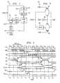
- FIG. 1illustrates a block diagram of a DRAM device
- FIG. 2illustrates an array portion of a DRAM device
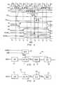
- FIG. 3shows a timing diagram for a read cycle of a DDR SDRAM
- FIG. 4shows a timing diagram for a write cycle of a DDR SDRAM
- FIG. 5shows a block diagram of the delayed column select line signal being used to access the memory array
- FIG. 6shows a block diagram of an alternate embodiment with a column select delay
- FIG. 7illustrates a schematic diagram of a delay circuit utilized to delay a column select line signal in accordance with an embodiment of the present invention.
- FIGS. 8 a - 8 gshow a detailed schematic diagram of an embodiment of a programmable delay circuit used to delay the column select line signal in accordance with an embodiment of the present invention.
- DRAM device architecture and design implementation issueswill first be discussed, followed by a description of preferred embodiments of the present invention and a discussion of some advantages thereof. Although each figure shows certain elements for purposes of discussion, many other components of a memory device may be present in the semiconductor devices shown.
- the present inventionis related to a paper written by, amongst others, each of the inventors. This paper is entitled “A 110 nm 512 Mb DDR DRAM with Vertical Transistor Trench Cell,” 2002 Symposium on VLSI Circuits, Digest of Technical Papers, June 2002, p. 114. This paper is incorporated herein by reference.
- FIG. 1illustrates a functional block diagram of a DRAM device 10 .
- an address selection signal ADDRis transmitted to a Column Address Buffer (CAB) 16 and Row Address Buffer (RAB) 20 .
- CABColumn Address Buffer
- RABRow Address Buffer
- the column address and row addressshare external pins so that the row address is received at a first time and the column address is received at a second time.
- the ADDR signalsmay be transmitted by an external device, such as a memory controller (not shown), for example.
- the column address buffer 16 and row address buffer 20are adapted to buffer the address signal.
- the outputs of the column address buffer 16 and row address buffer 20are coupled to a column decoder 14 and row decoder 18 , respectively.
- the column and row decoders 14 and 18are adapted to decode the signals received from the column address buffer 16 and row address buffer 20 , respectively, to provide the signal input to the array 12 , such that the selected row and column can be selected.
- the column address buffer 16includes a variable delay that will vary the addressing path time depending upon whether the operation is a read or a write.
- the column and row decoders 14 and 18are shown as single blocks. It should be understood, however, that the column and row decoders 14 and 18 may carry out several levels of predecoding and decoding. Some or all (or none) of these levels may be clocked.
- Data D that is addressed in array 12will be written into memory 12 or read from memory 12 via data buffer (DB) 17 .
- DBdata buffer
- the data buffer 17 and associated lineare provided to represent the read and write path, which may include a large number of lines and other components (e.g., secondary sense amplifiers).
- FIG. 1also shows a clock input CLK to illustrate that the memory device could be synchronous. To further illustrate this point the clock signal CLK is provided to each of the blocks. It is understood that while the external clock could be provided to various elements in the array, a number of clocking signals, which may operate continuously or only when needed, may be derived from the clock.
- FIG. 2shows more detail of the memory array 12 .
- the memory array 12includes a plurality of memory cells arranged in a matrix-type architecture or array.
- Each cell C 0 , C 1 , C 2 . . . C nincludes an access transistor 28 , typically an n-channel metal oxide semiconductor field effect transistor (MOSFET), coupled in series with a capacitor 30 , shown in the inset of FIG. 2 .
- the gate of each access transistor 28is coupled to a wordline WL 0 , and one source/drain region of the transistor 28 is coupled to a bitline BL 0 , as shown.
- a second source/drain region of the transistor 28is coupled to one end of the storage capacitor 30 .
- the other end of the storage capacitor 30is coupled to a reference voltage, such as V BHL /2, for example.
- bitlinesare organized as bitline pairs, e.g., BL 0 and bBL 0 .
- Each bitline pair BL 0 /bBL 0is coupled to a sense amplifier 24 , which is configured to amplify the voltage difference between the two bitlines in a pair.
- Traditional mid-level sensingis accomplished using latch-type sense amplifiers with a bitline high level of 1.5 V.
- Equalization and pre-charge circuitry 22is also coupled between each bitline in a pair to provide the proper initial voltages on the bitlines.
- the DRAM device 10includes four 128 Mb memory quadrants, each of which corresponds to an individual logical bank.
- Each 128 Mb bankmay be physically separated into a number of blocks, e.g., 16 blocks, each with 8 Mb in a folded bitline configuration.
- a blockmay comprise 1024 local wordlines.
- the blocksmay be separated by stripes of 4 k sense amplifiers on the right and left sides, which are shared by neighboring blocks.
- Each blockmay then be divided into 16 sections by rowgaps with each section containing 512 kb.
- a local data line (LDQ)spans two sections so that, in the column direction, the sections are paired, forming eight column segments.
- LDQlocal data line
- bitlinesare pre-charged to an initial value, typically one half of the value of a physical one written into a cell.
- this voltage levelis referred to as V BLH (bitline high) and is about 1.5 V.
- V BLHis generated on-chip.
- the equalization circuitry 22is provided to ensure that each bitline in a pair is pre-charged to the same level, e.g., V BLH /2 or about 0.75 V.
- the pre-charge and equalization circuitry 22is enabled by a signal EQL.
- V PPa high voltage (e.g., V PP ) is placed on a selected one of the wordlines WL. This signal will be generated by the row decoder 18 ( FIG. 1 ).
- V PPis derived from the external supply voltage.
- the high voltage on the wordlinewill cause the pass transistor of each memory cell coupled to that wordline to be conductive. Accordingly, charge will travel either to the bitline from the memory cell (in the case of a physical one, e.g., V BHL ) or from the bitline to the memory cell (in the case of a physical zero, e.g., 0V).
- the sense amplifier 24when activated by signal SET, will sense the physical one or zero and generate a differential voltage that corresponds with the signal read from the cell.
- a pair of pass transistors 26is provided between each column and the local input/output lines I/O and bI/O. Since the sense amplifier 24 associated with each column (only BL 0 /bBL 0 and BL 1 /bBL 1 are shown) will generate a bit that corresponds to cell associated with the selected row (as determined by the selected wordline), a column select signal CSL n is provided to the pass transistors 26 to select one of the columns, which is coupled to the local I/O. (Of course, some architectures will include multiple I/O's in which case a single select signal CSL n is coupled to the pass transistors 26 of more than one column.)
- a secondary sense amplifier (SSA) 25is coupled to each I/O line to amplify the voltage level.
- the SSA 25is timed off of the logic which enabled the CSL.
- this circuitrycontains not only a sense amplifier for reading, but also write buffers for driving the I/O lines.
- the “SSA”can be in one of three states: precharged (if no read or write), reading, or writing.
- the CSLsWhen a read command is issued, the CSLs get activated, and the sense amplifiers (basically clocked latches) are connected to the I/O lines. The clocking of the latches is synchronized with the CSL activation.
- the CSLsWhen a write command is issued, the CSLs are again activated, but the sense amplifier is disconnected from the I/O lines and the write drivers are connected instead. As in the case of a read, the clocking of the drivers is synchronized with the CSL activation.
- a write operationwill be performed in a similar fashion as a read.
- a wordlinemust have been previously activated, e.g., a bank is active.
- datais placed on the I/O lines and the CSLs are activated. This overwrites the primary sense amplifier, causing the BL and bBL to change (only in the case of a different data state) and the data is transferred to the memory cell.
- DDRDouble Data Rate SDRAM Specifications JESD79, DDR3332.5-3.3 and DDR 266 2-2-2, which are incorporated herein by reference.
- FIG. 3shows a timing diagram for a read cycle for a DDR SDRAM device.
- a write cycleis shown in FIG. 4 .
- a bankactivate reads all of the bits in the cells of a selected row and stores them in the sense amplifiers. An entire page of data (e.g., 4 k or 8 k bits, depending on the page length) is stored.
- An activate commandcan be seen as an internal read command.
- the read operationwill be described.
- the bitlines BL/bBLare pre-charged and equalized to a value of V BLH /2 and the sense amplifier 24 is disabled. Accordingly, the pre-charge/equalization enable signal EQL is high and the sense amplifier enable signal SET is low.
- the rows of the array 12are decoded by the row path, e.g., in response to a bank activate command ACT, which is recognized upon the rising edge of clock signal CLK at time t 1 .
- the signal line labeled CMDmay be derived from a number of pins, e.g., a read pin, a write pin, and/or a clock/enable pin, according to the device specifications, which are decoded to provide a particular command.
- the bank activationcauses signal EQL to go low, thereby causing the equalization circuitry 22 to be disabled in the specified sub-block.
- the row decoder 18will select one of the wordlines WL, which will rise.
- a differential signaldevelops on the bitlines BL/bBL.
- the sense amplifieris activated by signal SET and the differential signal is amplified by each primary sense amplifier 24 in a stripe of sense amplifiers.
- the read command READcan be issued as soon as two clock cycles after activate command ACT, in this case at time t 3 .
- the time between the activate command ACT and the read command READi.e., the time between t 1 and t 3
- t RCDthe time from row to column delay
- t RCD minimumthe time from row to column delay
- the READ commandcauses the selection of the appropriate column.
- the column select line CSL signalconnects the selected column, typically through the primary sense amplifier, to the local I/O's, which carry a differential signal to the secondary sense amplifier (not shown). From here, the data can be routed to the output DQ.
- CSL n and CSL n+1Internal control circuitry, not shown, will cause the activation of CSLs for each data prefetch. Due to architecture constraints, more than one CSL may be required to prefetch enough data for a particular I/O width. Thus, two CSL lines (labeled CSL n and CSL n+1 ) are shown. FIG. 3 shows four data words being read out. Since the illustrated device is a double-data rate device, two data words are read on each clock cycle.
- the pre-charge cyclecan be initiated by issuing a pre-charge command PRE at time t 7 .
- the pre-charge commandwill cause the wordline to turn off (i.e., WL goes low) thereby isolating all memory cells from the bitlines.
- the sense amplifiers 24are deactivated by switching the signal SET to a low value and the pre-charge and equalization circuitry 22 is activated by switching the signal EQL to a high value. This sequence will cause the bitlines to be set to the precharge voltage of V BLH /2.
- FIG. 3also shows the start of a second read cycle, which includes an activate command ACT received at time t 9 and a read command READ received at time t 11 .
- the second read cycleoperates in the same manner as the first read cycle.
- FIG. 4illustrates a write cycle, which is similar to a read cycle.
- a bank activate command ACTis issued at time t 1 , which decodes the x-direction and selects the wordline WL.
- the write command WRTis applied as soon as two clock cycles later, at time t 3 .
- the data DQis latched, so the rising edge of the clock CLK brings the first bit of data and the falling edge brings the second bit of data.
- the following rising edge of the clockbrings the third bit and the falling edge brings the fourth bit.
- the rising edge of the clock two cycles laterwill cause the column select signal CSL n to go high.
- the sense amplifier 24 and the cellare written to.
- bits 0 and 1are written when the CSL n signal goes high
- bits 2 and 3are written when the CSL n+1 signal goes high.
- the DDR SDRAM specificationrequires, that from the rising edge of the clock after the last bit of data (t 6 ), there must be two clock cycles before another pre-charge cycle can occur at time t 8 . Note that the CSL signal goes high into the first clock cycle of this wait period, e.g., between t 6 and t 7 . The data must be fully written into the cell before the wordline WL can be turned off.
- the Row to Column Delay(t RCD ) is defined as the minimum delay between a bank activate and a read command. The minimum is two clock cycles.
- the CAS latency(CL) is the timing, in clock cycles, between receipt of a read command and the time data is valid. The CAS latency can be either 1.5, 2, 2.5 or 3 clock cycles.
- any delay in the column pathis detrimental to the write-back time.
- the datahas less time to propagate from the DQ pins through the I/O lines to the sense amplifier 24 and the bitlines, and then to settle in the cell. This issue can be seen with reference to FIG. 4 .
- T 1a first time period
- the datatravels from the DQ pins to the local I/O's.
- the CSL signalis activated, the data is applied to the column, e.g., sense amplifier 24 , where it can be written to the cells. This happens in the period labeled T 2 . In typical embodiments, this time may be about 1 or 2 ns after the CSL signal is activated.
- the read timing requirementswanted the CSL signal to be delayed. This shift, however, would be detrimental in the write cycle. If CSL were delayed in time for a WRITE, there would be less time for the bitlines and cell to charge up, so that data would not be fully written into the memory cells. In other words, for the write operation, it is desirable that the CSL signal be activated early in the cycle. The severity of this problem is dependent upon the actual device configuration and speed requirement. For example, for a DDR PC333 having a clock frequency of 166 MHz, and a t RCD of 2.5, the timings are relaxed.
- the column activationis delayed in favor of the bank activation for a read command, while the column activation for the write command is kept faster, in order to maintain a full write back.
- the time interval t RCDis improved by delaying the time that a read cycle takes to activate the CSL.
- the CSL signalis delayed so that the column selection actually occurs later.
- This techniqueis achievable in memory devices having an independent column path between a read path and a write path.
- there is margin to delay the CSL signal for a read cyclea delay is not desirable in a write cycle. Because of the physical structure of the array wordlines and bitlines, the column path is faster than the row path; therefore, the column access time is artificially slowed down to achieve an improved row access time.
- the time from the rising edge of the clock at t 2 when a read or write command is received, to the time when the signal CSL is activated,is delayed during a read but not during a write.
- the amount of CSL delay for a read cyclecan be tuned in order to optimize the yield, e.g., to balance the t RCD and t RP .
- a programmable delay circuitcan be provided, so that completed memory devices can be tested, and then when the desired delay is determined, the device can be either temporarily or permanently programmed with a CSL delay for a read cycle.
- FIG. 5shows a block diagram of a preferred embodiment implementation of the circuit of the preferred invention.
- the column address pathextends from the address pins ADDR to the column address buffer 16 to the column decoder 14 , which provides the CSL control signals to the array 12 .
- the column decoder 14is enabled by a clock signal CKA 0 .
- the CKA 0 clock signalis provided by a variable delay circuit 32 .
- the CKA 0 clock signalis also applied to the secondary sense amplifier 25 .
- the delay circuit 32receives two inputs.
- the clock signal CLKBST(burst clock) represents an undelayed version of the column decoder enable clock.
- the R/W′ (read/write) control signaldetermines the delay, preferably selecting between one of two choices.
- the input clock signal CLKBSTis passed through as the output clock CKA 0 .
- the RIW′ control signalindicates a read operation
- the clock signal CKA 0is a delayed version of the input clock CLKBST.
- the amount of the delaycan be determined according to the specific timing of the circuit.
- FIG. 6illustrates an alternate embodiment.
- the delay circuit 32is put in the CSL signal path, as opposed to in the path of the enable signal.
- This embodimentcan be used in the case of both clocked decoders and unclocked (asynchronous) decoders. As before, the timing of the CSL signal will be adjusted depending upon the value of the read/write control signal.
- FIG. 7illustrates a schematic diagram of a variable delay circuit 32 that can be used in either of the embodiments of FIG. 5 or 6 .
- the input signal CLKBST(or CSL′ for the FIG. 6 embodiment) is provided to two paths. In the top path, the signal is coupled directly to transmission gate 34 , which is conducting when the R/W′ signal is low (indicating a write cycle).
- the input CLKBSTis also coupled to a delay element 40 , which is in turn coupled to a second transmission gate 36 .
- Transmission gate 36is conductive when the R/W′ signal is high (indicating a read cycle).
- the outputs of the transmission gates 34 and 36are tied together to provide the output signal CKA 0 (or CSL). While transmission gates 34 and 36 are illustrated, it is understood that any tri-state driver can be used.
- FIGS. 8 a - 8 gshow a detailed schematic diagram of an embodiment of a programmable delay circuit 32 used to delay the CKA 0 signal in accordance with an embodiment of the present invention.
- the main difference between FIG. 8 a and FIG. 7is the implementation of the delay element 40 .
- the delay element 40is divided between a plurality of delay segments 42 .
- each delay segment 42is implemented with two inverters.
- other delayscan be used.
- more than two inverterscan be used and/or capacitors (not shown) can be coupled between the inverters.
- the clock signal CLKBSTcan be routed so that it is delayed by all four of the delay segments 42 or only some (or none) of the delay elements 42 .
- this routingis implemented by a plurality of transmission gates 44 , which are controlled by control signals TMCDLY, dly 0 , dly 1 , dly 2 , dly 3 , and their inverses.
- the delay signals dlynare determined by TMCDLY and two other control signals TMC 0 and TMC 1 .
- TMCDLYTMC 0 and TMC 1
- Table 1provides the delay options for the particular embodiment shown in FIG. 8 a .
- the delay signals dlyn that control the transmission gates 44can be generated using combinational logic as shown in FIGS. 8 b - 8 g .
- the delaymay be adjusted in increments ranging from about 300 ps to about 400 ps. These delays are determined by the delay values of each delay segment 42 . Each segment can have the same amount of delay or a different amount of delay. In addition, the routing can be made as simple or complex as necessary to achieve the desired precision of delay. For example, the delay elements 42 could have values of 100 ps, 200 ps, 400 ps and 800 ps and transmission gates could be included between each delay segment 42 so that any combination of the delays is achievable. This embodiment would complicate the circuitry but would also allow any delay between zero and 1500 ps, within a 100 ps accuracy.
- the delay circuit 40may be tuned by varying the two signals TMC 1 and TMC 0 , which may be entered in a different test mode. It will be understood that any number of delay set-points may be generated.
- the amount of delay the delay circuit 40 producesis preferably changeable and/or programmable in a test mode. For example, after the memory device is fabricated, the delay may be iteratively tested to optimize the device performance. When an ideal amount of delay is determined, the device may include fuses which may be blown to store a programmed amount of delay. In this embodiment, any time the device is powered up, it will have the same amount of read cycle delay. Alternatively, the programming may be set up at start-up, or the device may be programmed by the user.
- the read delayis preferably adjustable in steps from 0 ns to approximately 1.5 ns, and the delay is controlled by fusable test modes. In this manner, advantageously, it is possible to customize the timing for different device configurations. For example, in FIG. 7 , the delay is adjustable in four 400 ps steps using fusable test modes.
- Embodiments of the present inventionprovide several advantages over prior art memory devices.
- a selective column path speed for read/write cyclesis provided that balances t RCD and T WR for chip speed optimization.
- the column activation delay controlis programmable by a fusable test mode.
- the inventionhas been described herein with particular relevance to the application of a DDR SDRAM; however, the novel concept of delaying the read CSL signal while not delaying the write CSL signal also has application in other semiconductor memory devices, such as other DRAM devices, static RAM (SRAM) devices, flash memories, resistive memory devices such as magnetic random access memories (MRAMs), and non-volatile memories such as electrically programmable read-only-memories (EPROMs), electrically erasable programmable read-only-memories (EEPROMs), and flash memory as examples.
- DRAMdynamic RAM
- MRAMsmagnetic random access memories
- EPROMselectrically programmable read-only-memories
- EEPROMselectrically erasable programmable read-only-memories
- the illustrated embodimentshave also assumed a stand-alone chip, where the address and data are provided from external sources.
- the present inventionalso applies to embedded memory where the memory array is included on the same substrate (or within the same package) as other control logic, such as a processor core or controller.
Landscapes
- Engineering & Computer Science (AREA)
- Microelectronics & Electronic Packaging (AREA)
- Computer Hardware Design (AREA)
- Dram (AREA)
Abstract
Description
- This is a continuation of U.S. application Ser. No. 10/285,027, filed Oct. 31, 2002, which application is hereby incorporated herein by reference.
- The present invention relates generally to the fabrication of semiconductor devices, and more particularly to the fabrication of memory devices.
- Semiconductor devices are used for integrated circuits in a variety of electrical and electronic applications, such as computers, cellular telephones, radios, and televisions. One particular type of semiconductor device is a semiconductor storage device, such as a random access memory (RAM) device. RAM devices use an electrical charge to store information. Many RAM devices include many storage cells arranged in a two-dimensional array with two sets of select lines, wordlines and bitlines. An individual storage cell is selected by activating its wordline and its bitline. RAM devices are considered “random access” because any memory cell in an array can be accessed directly if the row and column that intersect at that cell are known.
- A commonly used form of RAM is known as a dynamic RAM (DRAM) device. Dynamic random access memory has memory cells with a paired transistor and capacitor, wherein the capacitor requires periodic refreshing. One particular type of DRAM device is a synchronous DRAM (SDRAM) device, in which the memory cells are accessed synchronously. Synchronous dynamic random access memory often takes advantage of the burst mode concept to greatly improve performance by staying on the row containing the requested bit and moving rapidly through the columns. To achieve a high speed operation, a double data rate (DDR) architecture is often used, during which two data transfers are made per clock cycle, one upon the rising edge of the clock and the other upon the falling edge.
- Embodiments of the present invention achieve technical advantages as a method and structure for selectively delaying the column activation for a read command, but not for a write command, in order to optimize device speed. A programmable delay circuit is utilized to create a delay for the read signal, while the write path is designed for maximum speed. The speed of the device is optimized by balancing the minimum delay between a bank activate and a read command and the minimum timing between a read command and a precharge command.
- In one aspect, the present invention proposes to delay the column activation in favor of the bank activation for a read command, but to keep the faster column activation for the write command to maintain a full write back. Depending upon whether the device is operating in the read or write mode, it is possible to delay the column clock. This clock feeds into the column and data path and activates the column select, the secondary sense amplifier and the data path control. It is preferred that the write path be designed for maximum speed. The read path, however, can be slowed down by adding delay inverter stages, for example.
- In a first embodiment, a memory device includes an array of memory cells arranged in rows and columns. Preferably, each memory cell includes a pass transistor coupled to a storage capacitor. A row decoder is coupled to rows of memory cells while a column decoder is coupled to columns of the memory cells. The column decoder includes an enable input. A variable delay has an output coupled to the enable input of the column decoder. The variable delay receives an indication of whether a current cycle is a read cycle or a write cycle. In the preferred embodiment, a signal provided at the output of the variable delay is delayed if the current cycle is a read cycle compared to if the current cycle is a write cycle.
- Advantages of the invention include optimizing SDRAM device speed by selectively delaying the read cycle. The tRCDand tWRsignals are optimized, improving device performance. The artificial delay in the column path, in particular the column select line (CSL) signal and secondary sense amplifier activation, allows more time for signal development and amplification during a read command. A maximum operating efficiency may be achieved in accordance with the present invention.
- The above features of the present invention will be more clearly understood from consideration of the following descriptions in connection with accompanying drawings in which:
FIG. 1 illustrates a block diagram of a DRAM device;FIG. 2 illustrates an array portion of a DRAM device;FIG. 3 shows a timing diagram for a read cycle of a DDR SDRAM;FIG. 4 shows a timing diagram for a write cycle of a DDR SDRAM;FIG. 5 shows a block diagram of the delayed column select line signal being used to access the memory array;FIG. 6 shows a block diagram of an alternate embodiment with a column select delay;FIG. 7 illustrates a schematic diagram of a delay circuit utilized to delay a column select line signal in accordance with an embodiment of the present invention; andFIGS. 8 a-8gshow a detailed schematic diagram of an embodiment of a programmable delay circuit used to delay the column select line signal in accordance with an embodiment of the present invention.- The making and using of the presently preferred embodiments are discussed in detail below. It should be appreciated, however, that the present invention provides many applicable inventive concepts that can be embodied in a wide variety of specific contexts. The specific embodiments discussed are merely illustrative of specific ways to make and use the invention, and do not limit the scope of the invention.
- DRAM device architecture and design implementation issues will first be discussed, followed by a description of preferred embodiments of the present invention and a discussion of some advantages thereof. Although each figure shows certain elements for purposes of discussion, many other components of a memory device may be present in the semiconductor devices shown.
- The present invention is related to a paper written by, amongst others, each of the inventors. This paper is entitled “A 110 nm 512 Mb DDR DRAM with Vertical Transistor Trench Cell,” 2002 Symposium on VLSI Circuits, Digest of Technical Papers, June 2002, p. 114. This paper is incorporated herein by reference.
FIG. 1 illustrates a functional block diagram of aDRAM device 10. To access a particular cell in thearray 12, an address selection signal ADDR is transmitted to a Column Address Buffer (CAB)16 and Row Address Buffer (RAB)20. In a typical DRAM chip, the column address and row address share external pins so that the row address is received at a first time and the column address is received at a second time. The ADDR signals may be transmitted by an external device, such as a memory controller (not shown), for example.- The
column address buffer 16 androw address buffer 20 are adapted to buffer the address signal. The outputs of thecolumn address buffer 16 androw address buffer 20 are coupled to acolumn decoder 14 androw decoder 18, respectively. The column androw decoders column address buffer 16 androw address buffer 20, respectively, to provide the signal input to thearray 12, such that the selected row and column can be selected. In the preferred embodiment, thecolumn address buffer 16 includes a variable delay that will vary the addressing path time depending upon whether the operation is a read or a write. - In
FIG. 1 , the column androw decoders row decoders - Data D that is addressed in
array 12 will be written intomemory 12 or read frommemory 12 via data buffer (DB)17. Once again, this portion ofFIG. 1 is simplified. Thedata buffer 17 and associated line are provided to represent the read and write path, which may include a large number of lines and other components (e.g., secondary sense amplifiers). FIG. 1 also shows a clock input CLK to illustrate that the memory device could be synchronous. To further illustrate this point the clock signal CLK is provided to each of the blocks. It is understood that while the external clock could be provided to various elements in the array, a number of clocking signals, which may operate continuously or only when needed, may be derived from the clock.FIG. 2 shows more detail of thememory array 12. As shown inFIG. 2 , thememory array 12 includes a plurality of memory cells arranged in a matrix-type architecture or array. Each cell C0, C1, C2. . . Cnincludes anaccess transistor 28, typically an n-channel metal oxide semiconductor field effect transistor (MOSFET), coupled in series with acapacitor 30, shown in the inset ofFIG. 2 . The gate of eachaccess transistor 28 is coupled to a wordline WL0, and one source/drain region of thetransistor 28 is coupled to a bitline BL0, as shown. A second source/drain region of thetransistor 28 is coupled to one end of thestorage capacitor 30. The other end of thestorage capacitor 30 is coupled to a reference voltage, such as VBHL/2, for example.- The bitlines are organized as bitline pairs, e.g., BL0 and bBL0. Each bitline pair BL0/bBL0 is coupled to a
sense amplifier 24, which is configured to amplify the voltage difference between the two bitlines in a pair. Traditional mid-level sensing is accomplished using latch-type sense amplifiers with a bitline high level of 1.5 V. Equalization andpre-charge circuitry 22 is also coupled between each bitline in a pair to provide the proper initial voltages on the bitlines. - In a particular embodiment, the
DRAM device 10 includes four 128 Mb memory quadrants, each of which corresponds to an individual logical bank. Each 128 Mb bank may be physically separated into a number of blocks, e.g., 16 blocks, each with 8 Mb in a folded bitline configuration. There may be 512 bits for each bitline and the bitline-to-bitline noise can be minimized by twisting the bitlines. A block may comprise 1024 local wordlines. The blocks may be separated by stripes of 4 k sense amplifiers on the right and left sides, which are shared by neighboring blocks. Each block may then be divided into 16 sections by rowgaps with each section containing 512 kb. A local data line (LDQ) spans two sections so that, in the column direction, the sections are paired, forming eight column segments. - In operation, the bitlines are pre-charged to an initial value, typically one half of the value of a physical one written into a cell. In the preferred embodiment, this voltage level is referred to as VBLH(bitline high) and is about 1.5 V. Preferably, VBLHis generated on-chip. The
equalization circuitry 22 is provided to ensure that each bitline in a pair is pre-charged to the same level, e.g., VBLH/2 or about 0.75 V. The pre-charge andequalization circuitry 22 is enabled by a signal EQL. - To read a data bit from the array, a high voltage (e.g., VPP) is placed on a selected one of the wordlines WL. This signal will be generated by the row decoder18 (
FIG. 1 ). In a typical embodiment, VPPis derived from the external supply voltage. - The high voltage on the wordline will cause the pass transistor of each memory cell coupled to that wordline to be conductive. Accordingly, charge will travel either to the bitline from the memory cell (in the case of a physical one, e.g., VBHL) or from the bitline to the memory cell (in the case of a physical zero, e.g., 0V). The
sense amplifier 24, when activated by signal SET, will sense the physical one or zero and generate a differential voltage that corresponds with the signal read from the cell. - A pair of
pass transistors 26 is provided between each column and the local input/output lines I/O and bI/O. Since thesense amplifier 24 associated with each column (only BL0/bBL0and BL1/bBL1are shown) will generate a bit that corresponds to cell associated with the selected row (as determined by the selected wordline), a column select signal CSLnis provided to thepass transistors 26 to select one of the columns, which is coupled to the local I/O. (Of course, some architectures will include multiple I/O's in which case a single select signal CSLnis coupled to thepass transistors 26 of more than one column.) - A secondary sense amplifier (SSA)25 is coupled to each I/O line to amplify the voltage level. The
SSA 25 is timed off of the logic which enabled the CSL. In the preferred embodiment, this circuitry contains not only a sense amplifier for reading, but also write buffers for driving the I/O lines. Basically the “SSA” can be in one of three states: precharged (if no read or write), reading, or writing. - When a read command is issued, the CSLs get activated, and the sense amplifiers (basically clocked latches) are connected to the I/O lines. The clocking of the latches is synchronized with the CSL activation. When a write command is issued, the CSLs are again activated, but the sense amplifier is disconnected from the I/O lines and the write drivers are connected instead. As in the case of a read, the clocking of the drivers is synchronized with the CSL activation.
- A write operation will be performed in a similar fashion as a read. First, a wordline must have been previously activated, e.g., a bank is active. Subsequently, data is placed on the I/O lines and the CSLs are activated. This overwrites the primary sense amplifier, causing the BL and bBL to change (only in the case of a different data state) and the data is transferred to the memory cell.
- To be compliant with international standards for reading or writing data in or out of SDRAM devices, a sequence of timings must be met. For example, the majority of DRAMs sold today comply with the standards set by JEDEC (once known as the Joint Electron Device Engineering Council). See e.g., JEDEC Double Data Rate (DDR) SDRAM Specifications JESD79, DDR3332.5-3.3 and DDR 266 2-2-2, which are incorporated herein by reference.
FIG. 3 shows a timing diagram for a read cycle for a DDR SDRAM device. A write cycle is shown inFIG. 4 . In a JEDEC-compliant DRAM, a bank activate reads all of the bits in the cells of a selected row and stores them in the sense amplifiers. An entire page of data (e.g., 4 k or 8 k bits, depending on the page length) is stored. Upon receiving a read command, in a ×4 design or ×8 design, this number of bits, having already been latched, can be read. An activate command can be seen as an internal read command.- Referring first to
FIG. 3 , the read operation will be described. To begin, at time to, the bitlines BL/bBL are pre-charged and equalized to a value of VBLH/2 and thesense amplifier 24 is disabled. Accordingly, the pre-charge/equalization enable signal EQL is high and the sense amplifier enable signal SET is low. - To read data, the rows of the
array 12 are decoded by the row path, e.g., in response to a bank activate command ACT, which is recognized upon the rising edge of clock signal CLK at time t1. The signal line labeled CMD may be derived from a number of pins, e.g., a read pin, a write pin, and/or a clock/enable pin, according to the device specifications, which are decoded to provide a particular command. The bank activation causes signal EQL to go low, thereby causing theequalization circuitry 22 to be disabled in the specified sub-block. Also, therow decoder 18 will select one of the wordlines WL, which will rise. As a result of the rise of a selected wordline WL, a differential signal develops on the bitlines BL/bBL. After a delay time, the sense amplifier is activated by signal SET and the differential signal is amplified by eachprimary sense amplifier 24 in a stripe of sense amplifiers. - According to the JEDEC specification, the read command READ can be issued as soon as two clock cycles after activate command ACT, in this case at time t3. The time between the activate command ACT and the read command READ (i.e., the time between t1and t3) can be referred to as the time from row to column delay or tRCD. As noted above, the JEDEC DDR SDRAM standard specifies that tRCD minimum=2. A critical timing of a DRAM device is that the CSL signal must not go high until the
sense amplifier 24 is sufficiently set. The signal development time is the time from when the word line is activated until thesense amplifier 24 is ready to be activated. - The READ command causes the selection of the appropriate column. The column select line CSL signal connects the selected column, typically through the primary sense amplifier, to the local I/O's, which carry a differential signal to the secondary sense amplifier (not shown). From here, the data can be routed to the output DQ.
- Internal control circuitry, not shown, will cause the activation of CSLs for each data prefetch. Due to architecture constraints, more than one CSL may be required to prefetch enough data for a particular I/O width. Thus, two CSL lines (labeled CSLnand CSLn+1) are shown.
FIG. 3 shows four data words being read out. Since the illustrated device is a double-data rate device, two data words are read on each clock cycle. - After the wordline has been activated for a minimum amount of time, the wordline can be reset to begin another cycle. The pre-charge cycle can be initiated by issuing a pre-charge command PRE at time t7. The pre-charge command will cause the wordline to turn off (i.e., WL goes low) thereby isolating all memory cells from the bitlines. The
sense amplifiers 24 are deactivated by switching the signal SET to a low value and the pre-charge andequalization circuitry 22 is activated by switching the signal EQL to a high value. This sequence will cause the bitlines to be set to the precharge voltage of VBLH/2. FIG. 3 also shows the start of a second read cycle, which includes an activate command ACT received at time t9and a read command READ received at time t11. The second read cycle operates in the same manner as the first read cycle.FIG. 4 illustrates a write cycle, which is similar to a read cycle. To write data, a bank activate command ACT is issued at time t1, which decodes the x-direction and selects the wordline WL. The write command WRT is applied as soon as two clock cycles later, at time t3. One clock cycle later, the data DQ is latched, so the rising edge of the clock CLK brings the first bit of data and the falling edge brings the second bit of data. In a four-bit burst, the following rising edge of the clock brings the third bit and the falling edge brings the fourth bit. The rising edge of the clock two cycles later will cause the column select signal CSLnto go high. When the CSL signal is high, thesense amplifier 24 and the cell are written to. The data bits are written in pairs. Accordingly,bits 0 and1 (see BL/bBLn) are written when the CSLnsignal goes high, andbits 2 and3 (see BL/bBLn+1) are written when the CSLn+1signal goes high.- The DDR SDRAM specification requires, that from the rising edge of the clock after the last bit of data (t6), there must be two clock cycles before another pre-charge cycle can occur at time t8. Note that the CSL signal goes high into the first clock cycle of this wait period, e.g., between t6and t7. The data must be fully written into the cell before the wordline WL can be turned off.
- Two JEDEC specification timings are related to the read command. First, the Row to Column Delay (tRCD) is defined as the minimum delay between a bank activate and a read command. The minimum is two clock cycles. The CAS latency (CL) is the timing, in clock cycles, between receipt of a read command and the time data is valid. The CAS latency can be either 1.5, 2, 2.5 or 3 clock cycles.
- A problem exists in that there are conflicting demands in the timing for read and write operations of DDR SDRAM devices. For example, for a DDR PC266 SDRAM device, having a 133 MHz clock frequency, with a row to column delay of two (tRCD=2) and a CAS latency of two (CL=2), the 15 ns time (1/133 MHz*tRCD=15 ns) between bank activation and read command may not be sufficient for proper signal development and amplification before the read takes place. Therefore, an additional delay for the final column path activation is introduced, which means that part of the READ timing is taken to satisfy the signal development/amplifying process. Accordingly, less time is used to transfer the data from the primary sense amplifier to the DQ pins, a process initiated by the activation of the column select signal CSL. Referring to
FIG. 3 , this tradeoff can be visualized as moving the CSL signal to the right. - However, any delay in the column path is detrimental to the write-back time. During a write command, the data has less time to propagate from the DQ pins through the I/O lines to the
sense amplifier 24 and the bitlines, and then to settle in the cell. This issue can be seen with reference toFIG. 4 . During a first time period, labeled T1, the data travels from the DQ pins to the local I/O's. When the CSL signal is activated, the data is applied to the column, e.g.,sense amplifier 24, where it can be written to the cells. This happens in the period labeled T2. In typical embodiments, this time may be about 1 or 2 ns after the CSL signal is activated. - As noted above, the read timing requirements wanted the CSL signal to be delayed. This shift, however, would be detrimental in the write cycle. If CSL were delayed in time for a WRITE, there would be less time for the bitlines and cell to charge up, so that data would not be fully written into the memory cells. In other words, for the write operation, it is desirable that the CSL signal be activated early in the cycle. The severity of this problem is dependent upon the actual device configuration and speed requirement. For example, for a DDR PC333 having a clock frequency of 166 MHz, and a tRCDof 2.5, the timings are relaxed.
- In accordance with an embodiment of the present invention, the column activation is delayed in favor of the bank activation for a read command, while the column activation for the write command is kept faster, in order to maintain a full write back.
- In accordance with an embodiment of the invention, to produce a memory device having an increased operating frequency, the time interval tRCDis improved by delaying the time that a read cycle takes to activate the CSL. The CSL signal is delayed so that the column selection actually occurs later. This technique is achievable in memory devices having an independent column path between a read path and a write path. Although, as acknowledged in accordance with novel aspects of embodiments of the present invention, there is margin to delay the CSL signal for a read cycle, a delay is not desirable in a write cycle. Because of the physical structure of the array wordlines and bitlines, the column path is faster than the row path; therefore, the column access time is artificially slowed down to achieve an improved row access time.
- In accordance with a preferred embodiment of the present invention, the time from the rising edge of the clock at t2when a read or write command is received, to the time when the signal CSL is activated, is delayed during a read but not during a write. In a particular embodiment, the amount of CSL delay for a read cycle can be tuned in order to optimize the yield, e.g., to balance the tRCDand tRP. For example, a programmable delay circuit can be provided, so that completed memory devices can be tested, and then when the desired delay is determined, the device can be either temporarily or permanently programmed with a CSL delay for a read cycle.
FIG. 5 shows a block diagram of a preferred embodiment implementation of the circuit of the preferred invention. As inFIG. 1 , the column address path extends from the address pins ADDR to thecolumn address buffer 16 to thecolumn decoder 14, which provides the CSL control signals to thearray 12. In this example, thecolumn decoder 14 is enabled by a clock signal CKA0. The CKA0 clock signal is provided by avariable delay circuit 32. In this embodiment, the CKA0 clock signal is also applied to thesecondary sense amplifier 25.- The
delay circuit 32 receives two inputs. The clock signal CLKBST (burst clock) represents an undelayed version of the column decoder enable clock. The R/W′ (read/write) control signal determines the delay, preferably selecting between one of two choices. In the preferred embodiment, when the R/W′ control signal indicates a write operation, the input clock signal CLKBST is passed through as the output clock CKA0. On the other hand, when the RIW′ control signal indicates a read operation, the clock signal CKA0 is a delayed version of the input clock CLKBST. The amount of the delay can be determined according to the specific timing of the circuit. FIG. 6 illustrates an alternate embodiment. In this case, thedelay circuit 32 is put in the CSL signal path, as opposed to in the path of the enable signal. This embodiment can be used in the case of both clocked decoders and unclocked (asynchronous) decoders. As before, the timing of the CSL signal will be adjusted depending upon the value of the read/write control signal.FIG. 7 illustrates a schematic diagram of avariable delay circuit 32 that can be used in either of the embodiments ofFIG. 5 or6. The input signal CLKBST (or CSL′ for theFIG. 6 embodiment) is provided to two paths. In the top path, the signal is coupled directly totransmission gate 34, which is conducting when the R/W′ signal is low (indicating a write cycle). The input CLKBST is also coupled to adelay element 40, which is in turn coupled to asecond transmission gate 36.Transmission gate 36 is conductive when the R/W′ signal is high (indicating a read cycle). The outputs of thetransmission gates transmission gates FIGS. 8 a-8gshow a detailed schematic diagram of an embodiment of aprogrammable delay circuit 32 used to delay the CKA0 signal in accordance with an embodiment of the present invention. The main difference betweenFIG. 8 aandFIG. 7 is the implementation of thedelay element 40. InFIG. 8 a, thedelay element 40 is divided between a plurality ofdelay segments 42. In this example, eachdelay segment 42 is implemented with two inverters. In other embodiments, other delays can be used. For example, more than two inverters can be used and/or capacitors (not shown) can be coupled between the inverters.- The clock signal CLKBST can be routed so that it is delayed by all four of the
delay segments 42 or only some (or none) of thedelay elements 42. In this example, this routing is implemented by a plurality oftransmission gates 44, which are controlled by control signals TMCDLY, dly0, dly1, dly2, dly3, and their inverses. The delay signals dlyn are determined by TMCDLY and two other control signals TMC0 and TMC1. - In practice, the chip designer (or other user) will determine the desired amount of delay and program the control signals TMCDLY, TMC0 and TMC1 to the appropriate values to achieve the desired delay. Table 1 provides the delay options for the particular embodiment shown in
FIG. 8 a. The delay signals dlyn that control thetransmission gates 44 can be generated using combinational logic as shown inFIGS. 8 b-8g.TABLE 1 TMCDLY TMC1 TMC0 Added Delay 0 X X 0 1 0 0 300 ps 1 0 1 740 ps 1 1 0 1280 ps 1 1 1 1680 ps - In this embodiment, the delay may be adjusted in increments ranging from about 300 ps to about 400 ps. These delays are determined by the delay values of each
delay segment 42. Each segment can have the same amount of delay or a different amount of delay. In addition, the routing can be made as simple or complex as necessary to achieve the desired precision of delay. For example, thedelay elements 42 could have values of 100 ps, 200 ps, 400 ps and 800 ps and transmission gates could be included between eachdelay segment 42 so that any combination of the delays is achievable. This embodiment would complicate the circuitry but would also allow any delay between zero and 1500 ps, within a 100 ps accuracy. - The
delay circuit 40 may be tuned by varying the two signals TMC1 and TMC0, which may be entered in a different test mode. It will be understood that any number of delay set-points may be generated. - The amount of delay the
delay circuit 40 produces is preferably changeable and/or programmable in a test mode. For example, after the memory device is fabricated, the delay may be iteratively tested to optimize the device performance. When an ideal amount of delay is determined, the device may include fuses which may be blown to store a programmed amount of delay. In this embodiment, any time the device is powered up, it will have the same amount of read cycle delay. Alternatively, the programming may be set up at start-up, or the device may be programmed by the user. - In one embodiment, the read delay is preferably adjustable in steps from 0 ns to approximately 1.5 ns, and the delay is controlled by fusable test modes. In this manner, advantageously, it is possible to customize the timing for different device configurations. For example, in
FIG. 7 , the delay is adjustable in four 400 ps steps using fusable test modes. - Embodiments of the present invention provide several advantages over prior art memory devices. A selective column path speed for read/write cycles is provided that balances tRCDand TWRfor chip speed optimization. In one embodiment, the column activation delay control is programmable by a fusable test mode.
- The invention has been described herein with particular relevance to the application of a DDR SDRAM; however, the novel concept of delaying the read CSL signal while not delaying the write CSL signal also has application in other semiconductor memory devices, such as other DRAM devices, static RAM (SRAM) devices, flash memories, resistive memory devices such as magnetic random access memories (MRAMs), and non-volatile memories such as electrically programmable read-only-memories (EPROMs), electrically erasable programmable read-only-memories (EEPROMs), and flash memory as examples.
- The illustrated embodiments have also assumed a stand-alone chip, where the address and data are provided from external sources. The present invention, however, also applies to embedded memory where the memory array is included on the same substrate (or within the same package) as other control logic, such as a processor core or controller.
- While the invention has been described with reference to illustrative embodiments, this description is not intended to be construed in a limiting sense. Various modifications in combinations of the illustrative embodiments, as well as other embodiments of the invention, will be apparent to persons skilled in the art upon reference to the description.
Claims (17)
Priority Applications (1)
| Application Number | Priority Date | Filing Date | Title |
|---|---|---|---|
| US11/259,703US7149134B2 (en) | 2002-10-31 | 2005-10-26 | Memory device with column select being variably delayed |
Applications Claiming Priority (2)
| Application Number | Priority Date | Filing Date | Title |
|---|---|---|---|
| US10/285,027US7035150B2 (en) | 2002-10-31 | 2002-10-31 | Memory device with column select being variably delayed |
| US11/259,703US7149134B2 (en) | 2002-10-31 | 2005-10-26 | Memory device with column select being variably delayed |
Related Parent Applications (1)
| Application Number | Title | Priority Date | Filing Date |
|---|---|---|---|
| US10/285,027ContinuationUS7035150B2 (en) | 2002-10-31 | 2002-10-31 | Memory device with column select being variably delayed |
Publications (2)
| Publication Number | Publication Date |
|---|---|
| US20060050574A1true US20060050574A1 (en) | 2006-03-09 |
| US7149134B2 US7149134B2 (en) | 2006-12-12 |
Family
ID=32175067
Family Applications (2)
| Application Number | Title | Priority Date | Filing Date |
|---|---|---|---|
| US10/285,027Expired - Fee RelatedUS7035150B2 (en) | 2002-10-31 | 2002-10-31 | Memory device with column select being variably delayed |
| US11/259,703Expired - Fee RelatedUS7149134B2 (en) | 2002-10-31 | 2005-10-26 | Memory device with column select being variably delayed |
Family Applications Before (1)
| Application Number | Title | Priority Date | Filing Date |
|---|---|---|---|
| US10/285,027Expired - Fee RelatedUS7035150B2 (en) | 2002-10-31 | 2002-10-31 | Memory device with column select being variably delayed |
Country Status (2)
| Country | Link |
|---|---|
| US (2) | US7035150B2 (en) |
| DE (1) | DE10350865A1 (en) |
Cited By (40)
| Publication number | Priority date | Publication date | Assignee | Title |
|---|---|---|---|---|
| US20070014168A1 (en)* | 2005-06-24 | 2007-01-18 | Rajan Suresh N | Method and circuit for configuring memory core integrated circuit dies with memory interface integrated circuit dies |
| US20070058410A1 (en)* | 2005-09-02 | 2007-03-15 | Rajan Suresh N | Methods and apparatus of stacking DRAMs |
| US20070070792A1 (en)* | 2005-09-29 | 2007-03-29 | Hynix Semiconductor Inc. | Output controller with test unit |
| US20080025124A1 (en)* | 2006-07-31 | 2008-01-31 | Metaram, Inc. | Interface circuit system and method for performing power management operations utilizing power management signals |
| US20080025108A1 (en)* | 2006-07-31 | 2008-01-31 | Metaram, Inc. | System and method for delaying a signal communicated from a system to at least one of a plurality of memory circuits |
| US20080025137A1 (en)* | 2005-06-24 | 2008-01-31 | Metaram, Inc. | System and method for simulating an aspect of a memory circuit |
| US20080028135A1 (en)* | 2006-07-31 | 2008-01-31 | Metaram, Inc. | Multiple-component memory interface system and method |
| US20080025123A1 (en)* | 2006-07-31 | 2008-01-31 | Metaram, Inc. | Interface circuit system and method for autonomously performing power management operations in conjunction with a plurality of memory circuits |
| US20080025125A1 (en)* | 2006-07-31 | 2008-01-31 | Metaram, Inc. | Interface circuit system and method for performing power management operations in conjunction with only a portion of a memory circuit |
| US20080031072A1 (en)* | 2006-07-31 | 2008-02-07 | Metaram, Inc. | Power saving system and method for use with a plurality of memory circuits |
| US20080082763A1 (en)* | 2006-10-02 | 2008-04-03 | Metaram, Inc. | Apparatus and method for power management of memory circuits by a system or component thereof |
| US20080109206A1 (en)* | 2006-07-31 | 2008-05-08 | Rajan Suresh N | Memory device with emulated characteristics |
| US20080133820A1 (en)* | 2006-11-30 | 2008-06-05 | Ramkarthik Ganesan | DDR flash implementation with row buffer interface to legacy flash functions |
| US7581127B2 (en) | 2006-07-31 | 2009-08-25 | Metaram, Inc. | Interface circuit system and method for performing power saving operations during a command-related latency |
| US8055833B2 (en) | 2006-10-05 | 2011-11-08 | Google Inc. | System and method for increasing capacity, performance, and flexibility of flash storage |
| US8060774B2 (en) | 2005-06-24 | 2011-11-15 | Google Inc. | Memory systems and memory modules |
| US8077535B2 (en) | 2006-07-31 | 2011-12-13 | Google Inc. | Memory refresh apparatus and method |
| US8081474B1 (en) | 2007-12-18 | 2011-12-20 | Google Inc. | Embossed heat spreader |
| US8080874B1 (en) | 2007-09-14 | 2011-12-20 | Google Inc. | Providing additional space between an integrated circuit and a circuit board for positioning a component therebetween |
| US8090897B2 (en) | 2006-07-31 | 2012-01-03 | Google Inc. | System and method for simulating an aspect of a memory circuit |
| US8089795B2 (en) | 2006-02-09 | 2012-01-03 | Google Inc. | Memory module with memory stack and interface with enhanced capabilities |
| US8111566B1 (en) | 2007-11-16 | 2012-02-07 | Google, Inc. | Optimal channel design for memory devices for providing a high-speed memory interface |
| US8130560B1 (en) | 2006-11-13 | 2012-03-06 | Google Inc. | Multi-rank partial width memory modules |
| US8169233B2 (en) | 2009-06-09 | 2012-05-01 | Google Inc. | Programming of DIMM termination resistance values |
| US8209479B2 (en) | 2007-07-18 | 2012-06-26 | Google Inc. | Memory circuit system and method |
| US8244971B2 (en) | 2006-07-31 | 2012-08-14 | Google Inc. | Memory circuit system and method |
| US8280714B2 (en) | 2006-07-31 | 2012-10-02 | Google Inc. | Memory circuit simulation system and method with refresh capabilities |
| US8327104B2 (en) | 2006-07-31 | 2012-12-04 | Google Inc. | Adjusting the timing of signals associated with a memory system |
| US8335894B1 (en) | 2008-07-25 | 2012-12-18 | Google Inc. | Configurable memory system with interface circuit |
| US8386722B1 (en) | 2008-06-23 | 2013-02-26 | Google Inc. | Stacked DIMM memory interface |
| US8397013B1 (en) | 2006-10-05 | 2013-03-12 | Google Inc. | Hybrid memory module |
| US8438328B2 (en) | 2008-02-21 | 2013-05-07 | Google Inc. | Emulation of abstracted DIMMs using abstracted DRAMs |
| US8566516B2 (en) | 2006-07-31 | 2013-10-22 | Google Inc. | Refresh management of memory modules |
| US8796830B1 (en) | 2006-09-01 | 2014-08-05 | Google Inc. | Stackable low-profile lead frame package |
| US9171585B2 (en) | 2005-06-24 | 2015-10-27 | Google Inc. | Configurable memory circuit system and method |
| US9507739B2 (en) | 2005-06-24 | 2016-11-29 | Google Inc. | Configurable memory circuit system and method |
| US9542353B2 (en) | 2006-02-09 | 2017-01-10 | Google Inc. | System and method for reducing command scheduling constraints of memory circuits |
| US9632929B2 (en) | 2006-02-09 | 2017-04-25 | Google Inc. | Translating an address associated with a command communicated between a system and memory circuits |
| US10013371B2 (en) | 2005-06-24 | 2018-07-03 | Google Llc | Configurable memory circuit system and method |
| WO2022046304A1 (en)* | 2020-08-28 | 2022-03-03 | Micron Technology, Inc | Systems and methods for adaptive read training of three dimensional memory |
Families Citing this family (21)
| Publication number | Priority date | Publication date | Assignee | Title |
|---|---|---|---|---|
| US7841944B2 (en)* | 2002-08-06 | 2010-11-30 | Igt | Gaming device having a three dimensional display device |
| US7035150B2 (en)* | 2002-10-31 | 2006-04-25 | Infineon Technologies Ag | Memory device with column select being variably delayed |
| KR100586841B1 (en)* | 2003-12-15 | 2006-06-07 | 삼성전자주식회사 | Variable delay control method and circuit |
| US8688892B2 (en) | 2004-05-26 | 2014-04-01 | OCZ Storage Solutions Inc. | System and method for increasing DDR memory bandwidth in DDR SDRAM modules |
| US8151030B2 (en)* | 2004-05-26 | 2012-04-03 | Ocz Technology Group, Inc. | Method of increasing DDR memory bandwidth in DDR SDRAM modules |
| KR100868251B1 (en)* | 2007-03-22 | 2008-11-12 | 주식회사 하이닉스반도체 | Semiconductor memory device |
| KR100893577B1 (en)* | 2007-06-26 | 2009-04-17 | 주식회사 하이닉스반도체 | Semiconductor memory device |
| US8521979B2 (en) | 2008-05-29 | 2013-08-27 | Micron Technology, Inc. | Memory systems and methods for controlling the timing of receiving read data |
| US7979757B2 (en)* | 2008-06-03 | 2011-07-12 | Micron Technology, Inc. | Method and apparatus for testing high capacity/high bandwidth memory devices |
| US7855931B2 (en)* | 2008-07-21 | 2010-12-21 | Micron Technology, Inc. | Memory system and method using stacked memory device dice, and system using the memory system |
| US8289760B2 (en) | 2008-07-02 | 2012-10-16 | Micron Technology, Inc. | Multi-mode memory device and method having stacked memory dice, a logic die and a command processing circuit and operating in direct and indirect modes |
| US8756486B2 (en) | 2008-07-02 | 2014-06-17 | Micron Technology, Inc. | Method and apparatus for repairing high capacity/high bandwidth memory devices |
| US8127204B2 (en) | 2008-08-15 | 2012-02-28 | Micron Technology, Inc. | Memory system and method using a memory device die stacked with a logic die using data encoding, and system using the memory system |
| US8400808B2 (en) | 2010-12-16 | 2013-03-19 | Micron Technology, Inc. | Phase interpolators and push-pull buffers |
| US9081665B2 (en)* | 2012-02-02 | 2015-07-14 | OCZ Storage Solutions Inc. | Apparatus, methods and architecture to increase write performance and endurance of non-volatile solid state memory components |
| US9171597B2 (en) | 2013-08-30 | 2015-10-27 | Micron Technology, Inc. | Apparatuses and methods for providing strobe signals to memories |
| WO2017206000A1 (en)* | 2016-05-28 | 2017-12-07 | 华为技术有限公司 | Memory access method and memory controller |
| KR20180058478A (en)* | 2016-11-24 | 2018-06-01 | 에스케이하이닉스 주식회사 | Semiconductor device, semiconductor system including thereof and read and write operation method for the semiconductor device |
| KR102386811B1 (en)* | 2017-07-18 | 2022-04-15 | 에스케이하이닉스 주식회사 | Memory system and operating method thereof |
| CN116052737B (en)* | 2023-03-28 | 2023-08-29 | 长鑫存储技术有限公司 | Column control circuit and memory device |
| CN117809708B (en)* | 2024-02-29 | 2024-05-07 | 浙江力积存储科技有限公司 | Storage array and method for improving data reading accuracy of storage array |
Citations (3)
| Publication number | Priority date | Publication date | Assignee | Title |
|---|---|---|---|---|
| US6134179A (en)* | 1998-05-22 | 2000-10-17 | Mitsubishi Denki Kabushiki Kaisha | Synchronous semiconductor memory device capable of high speed reading and writing |
| US6269031B1 (en)* | 1999-07-19 | 2001-07-31 | Nec Corporation | Semiconductor memory device |
| US20040088475A1 (en)* | 2002-10-31 | 2004-05-06 | Infineon Technologies North America Corp. | Memory device with column select being variably delayed |
- 2002
- 2002-10-31USUS10/285,027patent/US7035150B2/ennot_activeExpired - Fee Related
- 2003
- 2003-10-31DEDE10350865Apatent/DE10350865A1/ennot_activeCeased
- 2005
- 2005-10-26USUS11/259,703patent/US7149134B2/ennot_activeExpired - Fee Related
Patent Citations (3)
| Publication number | Priority date | Publication date | Assignee | Title |
|---|---|---|---|---|
| US6134179A (en)* | 1998-05-22 | 2000-10-17 | Mitsubishi Denki Kabushiki Kaisha | Synchronous semiconductor memory device capable of high speed reading and writing |
| US6269031B1 (en)* | 1999-07-19 | 2001-07-31 | Nec Corporation | Semiconductor memory device |
| US20040088475A1 (en)* | 2002-10-31 | 2004-05-06 | Infineon Technologies North America Corp. | Memory device with column select being variably delayed |
Cited By (93)
| Publication number | Priority date | Publication date | Assignee | Title |
|---|---|---|---|---|
| US9507739B2 (en) | 2005-06-24 | 2016-11-29 | Google Inc. | Configurable memory circuit system and method |
| US8359187B2 (en) | 2005-06-24 | 2013-01-22 | Google Inc. | Simulating a different number of memory circuit devices |
| US7609567B2 (en) | 2005-06-24 | 2009-10-27 | Metaram, Inc. | System and method for simulating an aspect of a memory circuit |
| US8060774B2 (en) | 2005-06-24 | 2011-11-15 | Google Inc. | Memory systems and memory modules |
| US7515453B2 (en) | 2005-06-24 | 2009-04-07 | Metaram, Inc. | Integrated memory core and memory interface circuit |
| US20070014168A1 (en)* | 2005-06-24 | 2007-01-18 | Rajan Suresh N | Method and circuit for configuring memory core integrated circuit dies with memory interface integrated circuit dies |
| US20080025137A1 (en)* | 2005-06-24 | 2008-01-31 | Metaram, Inc. | System and method for simulating an aspect of a memory circuit |
| US9171585B2 (en) | 2005-06-24 | 2015-10-27 | Google Inc. | Configurable memory circuit system and method |
| US8615679B2 (en) | 2005-06-24 | 2013-12-24 | Google Inc. | Memory modules with reliability and serviceability functions |
| US10013371B2 (en) | 2005-06-24 | 2018-07-03 | Google Llc | Configurable memory circuit system and method |
| US20070050530A1 (en)* | 2005-06-24 | 2007-03-01 | Rajan Suresh N | Integrated memory core and memory interface circuit |
| US8619452B2 (en) | 2005-09-02 | 2013-12-31 | Google Inc. | Methods and apparatus of stacking DRAMs |
| US8582339B2 (en) | 2005-09-02 | 2013-11-12 | Google Inc. | System including memory stacks |
| US7599205B2 (en) | 2005-09-02 | 2009-10-06 | Metaram, Inc. | Methods and apparatus of stacking DRAMs |
| US20070058410A1 (en)* | 2005-09-02 | 2007-03-15 | Rajan Suresh N | Methods and apparatus of stacking DRAMs |
| US8811065B2 (en) | 2005-09-02 | 2014-08-19 | Google Inc. | Performing error detection on DRAMs |
| US7379316B2 (en) | 2005-09-02 | 2008-05-27 | Metaram, Inc. | Methods and apparatus of stacking DRAMs |
| US20080170425A1 (en)* | 2005-09-02 | 2008-07-17 | Rajan Suresh N | Methods and apparatus of stacking drams |
| US7549092B2 (en)* | 2005-09-29 | 2009-06-16 | Hynix Semiconductor, Inc. | Output controller with test unit |
| US20070070792A1 (en)* | 2005-09-29 | 2007-03-29 | Hynix Semiconductor Inc. | Output controller with test unit |
| US9632929B2 (en) | 2006-02-09 | 2017-04-25 | Google Inc. | Translating an address associated with a command communicated between a system and memory circuits |
| US9727458B2 (en) | 2006-02-09 | 2017-08-08 | Google Inc. | Translating an address associated with a command communicated between a system and memory circuits |
| US8797779B2 (en) | 2006-02-09 | 2014-08-05 | Google Inc. | Memory module with memory stack and interface with enhanced capabilites |
| US8089795B2 (en) | 2006-02-09 | 2012-01-03 | Google Inc. | Memory module with memory stack and interface with enhanced capabilities |
| US8566556B2 (en) | 2006-02-09 | 2013-10-22 | Google Inc. | Memory module with memory stack and interface with enhanced capabilities |
| US9542352B2 (en) | 2006-02-09 | 2017-01-10 | Google Inc. | System and method for reducing command scheduling constraints of memory circuits |
| US9542353B2 (en) | 2006-02-09 | 2017-01-10 | Google Inc. | System and method for reducing command scheduling constraints of memory circuits |
| US7392338B2 (en) | 2006-07-31 | 2008-06-24 | Metaram, Inc. | Interface circuit system and method for autonomously performing power management operations in conjunction with a plurality of memory circuits |
| US20080126689A1 (en)* | 2006-07-31 | 2008-05-29 | Suresh Natarajan Rajan | Memory device with emulated characteristics |
| US7724589B2 (en) | 2006-07-31 | 2010-05-25 | Google Inc. | System and method for delaying a signal communicated from a system to at least one of a plurality of memory circuits |
| US7730338B2 (en) | 2006-07-31 | 2010-06-01 | Google Inc. | Interface circuit system and method for autonomously performing power management operations in conjunction with a plurality of memory circuits |
| US7761724B2 (en) | 2006-07-31 | 2010-07-20 | Google Inc. | Interface circuit system and method for performing power management operations in conjunction with only a portion of a memory circuit |
| US8019589B2 (en) | 2006-07-31 | 2011-09-13 | Google Inc. | Memory apparatus operable to perform a power-saving operation |
| US8041881B2 (en) | 2006-07-31 | 2011-10-18 | Google Inc. | Memory device with emulated characteristics |
| US20080025124A1 (en)* | 2006-07-31 | 2008-01-31 | Metaram, Inc. | Interface circuit system and method for performing power management operations utilizing power management signals |
| US7580312B2 (en) | 2006-07-31 | 2009-08-25 | Metaram, Inc. | Power saving system and method for use with a plurality of memory circuits |
| US8077535B2 (en) | 2006-07-31 | 2011-12-13 | Google Inc. | Memory refresh apparatus and method |
| US7581127B2 (en) | 2006-07-31 | 2009-08-25 | Metaram, Inc. | Interface circuit system and method for performing power saving operations during a command-related latency |
| US7472220B2 (en) | 2006-07-31 | 2008-12-30 | Metaram, Inc. | Interface circuit system and method for performing power management operations utilizing power management signals |
| US8090897B2 (en) | 2006-07-31 | 2012-01-03 | Google Inc. | System and method for simulating an aspect of a memory circuit |
| US20080239858A1 (en)* | 2006-07-31 | 2008-10-02 | Suresh Natarajan Rajan | Interface circuit system and method for autonomously performing power management operations in conjunction with a plurality of memory circuits |
| US8112266B2 (en) | 2006-07-31 | 2012-02-07 | Google Inc. | Apparatus for simulating an aspect of a memory circuit |
| US20080025108A1 (en)* | 2006-07-31 | 2008-01-31 | Metaram, Inc. | System and method for delaying a signal communicated from a system to at least one of a plurality of memory circuits |
| US8745321B2 (en) | 2006-07-31 | 2014-06-03 | Google Inc. | Simulating a memory standard |
| US8154935B2 (en) | 2006-07-31 | 2012-04-10 | Google Inc. | Delaying a signal communicated from a system to at least one of a plurality of memory circuits |
| US7386656B2 (en) | 2006-07-31 | 2008-06-10 | Metaram, Inc. | Interface circuit system and method for performing power management operations in conjunction with only a portion of a memory circuit |
| US8868829B2 (en) | 2006-07-31 | 2014-10-21 | Google Inc. | Memory circuit system and method |
| US8244971B2 (en) | 2006-07-31 | 2012-08-14 | Google Inc. | Memory circuit system and method |
| US8280714B2 (en) | 2006-07-31 | 2012-10-02 | Google Inc. | Memory circuit simulation system and method with refresh capabilities |
| US8327104B2 (en) | 2006-07-31 | 2012-12-04 | Google Inc. | Adjusting the timing of signals associated with a memory system |
| US20080126687A1 (en)* | 2006-07-31 | 2008-05-29 | Suresh Natarajan Rajan | Memory device with emulated characteristics |
| US8340953B2 (en) | 2006-07-31 | 2012-12-25 | Google, Inc. | Memory circuit simulation with power saving capabilities |
| US7590796B2 (en) | 2006-07-31 | 2009-09-15 | Metaram, Inc. | System and method for power management in memory systems |
| US8972673B2 (en) | 2006-07-31 | 2015-03-03 | Google Inc. | Power management of memory circuits by virtual memory simulation |
| US20080109206A1 (en)* | 2006-07-31 | 2008-05-08 | Rajan Suresh N | Memory device with emulated characteristics |
| US8671244B2 (en) | 2006-07-31 | 2014-03-11 | Google Inc. | Simulating a memory standard |
| US9047976B2 (en) | 2006-07-31 | 2015-06-02 | Google Inc. | Combined signal delay and power saving for use with a plurality of memory circuits |
| US8631220B2 (en) | 2006-07-31 | 2014-01-14 | Google Inc. | Adjusting the timing of signals associated with a memory system |
| US8566516B2 (en) | 2006-07-31 | 2013-10-22 | Google Inc. | Refresh management of memory modules |
| US20080031072A1 (en)* | 2006-07-31 | 2008-02-07 | Metaram, Inc. | Power saving system and method for use with a plurality of memory circuits |
| US20080025125A1 (en)* | 2006-07-31 | 2008-01-31 | Metaram, Inc. | Interface circuit system and method for performing power management operations in conjunction with only a portion of a memory circuit |
| US8595419B2 (en) | 2006-07-31 | 2013-11-26 | Google Inc. | Memory apparatus operable to perform a power-saving operation |
| US8601204B2 (en) | 2006-07-31 | 2013-12-03 | Google Inc. | Simulating a refresh operation latency |
| US20080025123A1 (en)* | 2006-07-31 | 2008-01-31 | Metaram, Inc. | Interface circuit system and method for autonomously performing power management operations in conjunction with a plurality of memory circuits |
| US20080028135A1 (en)* | 2006-07-31 | 2008-01-31 | Metaram, Inc. | Multiple-component memory interface system and method |
| US8796830B1 (en) | 2006-09-01 | 2014-08-05 | Google Inc. | Stackable low-profile lead frame package |
| US20080082763A1 (en)* | 2006-10-02 | 2008-04-03 | Metaram, Inc. | Apparatus and method for power management of memory circuits by a system or component thereof |
| US8397013B1 (en) | 2006-10-05 | 2013-03-12 | Google Inc. | Hybrid memory module |
| US8977806B1 (en) | 2006-10-05 | 2015-03-10 | Google Inc. | Hybrid memory module |
| US8370566B2 (en) | 2006-10-05 | 2013-02-05 | Google Inc. | System and method for increasing capacity, performance, and flexibility of flash storage |
| US8751732B2 (en) | 2006-10-05 | 2014-06-10 | Google Inc. | System and method for increasing capacity, performance, and flexibility of flash storage |
| US8055833B2 (en) | 2006-10-05 | 2011-11-08 | Google Inc. | System and method for increasing capacity, performance, and flexibility of flash storage |
| US8446781B1 (en) | 2006-11-13 | 2013-05-21 | Google Inc. | Multi-rank partial width memory modules |
| US8130560B1 (en) | 2006-11-13 | 2012-03-06 | Google Inc. | Multi-rank partial width memory modules |
| US8760936B1 (en) | 2006-11-13 | 2014-06-24 | Google Inc. | Multi-rank partial width memory modules |
| US20080133820A1 (en)* | 2006-11-30 | 2008-06-05 | Ramkarthik Ganesan | DDR flash implementation with row buffer interface to legacy flash functions |
| US8209479B2 (en) | 2007-07-18 | 2012-06-26 | Google Inc. | Memory circuit system and method |
| US8080874B1 (en) | 2007-09-14 | 2011-12-20 | Google Inc. | Providing additional space between an integrated circuit and a circuit board for positioning a component therebetween |
| US8675429B1 (en) | 2007-11-16 | 2014-03-18 | Google Inc. | Optimal channel design for memory devices for providing a high-speed memory interface |
| US8111566B1 (en) | 2007-11-16 | 2012-02-07 | Google, Inc. | Optimal channel design for memory devices for providing a high-speed memory interface |
| US8081474B1 (en) | 2007-12-18 | 2011-12-20 | Google Inc. | Embossed heat spreader |
| US8705240B1 (en) | 2007-12-18 | 2014-04-22 | Google Inc. | Embossed heat spreader |
| US8730670B1 (en) | 2007-12-18 | 2014-05-20 | Google Inc. | Embossed heat spreader |
| US8631193B2 (en) | 2008-02-21 | 2014-01-14 | Google Inc. | Emulation of abstracted DIMMS using abstracted DRAMS |
| US8438328B2 (en) | 2008-02-21 | 2013-05-07 | Google Inc. | Emulation of abstracted DIMMs using abstracted DRAMs |
| US8386722B1 (en) | 2008-06-23 | 2013-02-26 | Google Inc. | Stacked DIMM memory interface |
| US8762675B2 (en) | 2008-06-23 | 2014-06-24 | Google Inc. | Memory system for synchronous data transmission |
| US8335894B1 (en) | 2008-07-25 | 2012-12-18 | Google Inc. | Configurable memory system with interface circuit |
| US8819356B2 (en) | 2008-07-25 | 2014-08-26 | Google Inc. | Configurable multirank memory system with interface circuit |
| US8169233B2 (en) | 2009-06-09 | 2012-05-01 | Google Inc. | Programming of DIMM termination resistance values |
| WO2022046304A1 (en)* | 2020-08-28 | 2022-03-03 | Micron Technology, Inc | Systems and methods for adaptive read training of three dimensional memory |
| US11340831B2 (en) | 2020-08-28 | 2022-05-24 | Micron Technology, Inc. | Systems and methods for adaptive read training of three dimensional memory |
| US11733915B2 (en) | 2020-08-28 | 2023-08-22 | Micron Technology, Inc. | Systems and methods for adaptive read training of three dimensional memory |
Also Published As
| Publication number | Publication date |
|---|---|
| US7035150B2 (en) | 2006-04-25 |
| DE10350865A1 (en) | 2004-05-27 |
| US7149134B2 (en) | 2006-12-12 |
| DE10350865A8 (en) | 2004-09-23 |
| US20040088475A1 (en) | 2004-05-06 |
Similar Documents
| Publication | Publication Date | Title |
|---|---|---|
| US7149134B2 (en) | Memory device with column select being variably delayed | |
| JP5400262B2 (en) | Semiconductor device | |
| KR100537237B1 (en) | Semiconductor memory device suppressing peak current | |
| US6134169A (en) | Semiconductor memory device | |
| US7561462B2 (en) | Circuit and method for a high speed dynamic RAM | |
| US7813211B2 (en) | Semiconductor memory device | |
| KR100902125B1 (en) | Dram for low power consumption and driving method thereof | |
| US6028812A (en) | Semiconductor memory device and method for controlling the same | |
| US6496403B2 (en) | Semiconductor memory device | |
| JP2009134840A (en) | Semiconductor memory device | |
| US6636443B2 (en) | Semiconductor memory device having row buffers | |
| US6731559B2 (en) | Synchronous semiconductor memory device | |
| US6885606B2 (en) | Synchronous semiconductor memory device with a plurality of memory banks and method of controlling the same | |
| US6166993A (en) | Synchronous semiconductor memory device | |
| US20040264260A1 (en) | Semiconductor memory device | |
| US7016235B2 (en) | Data sorting in memories | |
| JP4632121B2 (en) | Semiconductor memory device | |
| JP2004071119A (en) | Semiconductor memory device | |
| US6947340B2 (en) | Memory device for reducing skew of data and address | |
| US6930950B2 (en) | Semiconductor memory device having self-precharge function | |
| US20030123310A1 (en) | Semiconductor memory device having write column select gate | |
| US12266397B2 (en) | Amplification circuit, control method, and memory | |
| US11049534B2 (en) | Column control circuit and semiconductor device including the same | |
| KR100950578B1 (en) | Semiconductor memory device and driving method thereof | |
| JP2001067875A (en) | Output circuit |
Legal Events
| Date | Code | Title | Description |
|---|---|---|---|
| CC | Certificate of correction | ||
| AS | Assignment | Owner name:QIMONDA AG,GERMANY Free format text:ASSIGNMENT OF ASSIGNORS INTEREST;ASSIGNOR:INFINEON TECHNOLOGIES AG;REEL/FRAME:023768/0001 Effective date:20060425 Owner name:QIMONDA AG, GERMANY Free format text:ASSIGNMENT OF ASSIGNORS INTEREST;ASSIGNOR:INFINEON TECHNOLOGIES AG;REEL/FRAME:023768/0001 Effective date:20060425 | |
| FPAY | Fee payment | Year of fee payment:4 | |
| FPAY | Fee payment | Year of fee payment:8 | |
| AS | Assignment | Owner name:INFINEON TECHNOLOGIES AG, GERMANY Free format text:ASSIGNMENT OF ASSIGNORS INTEREST;ASSIGNOR:QIMONDA AG;REEL/FRAME:035623/0001 Effective date:20141009 | |
| AS | Assignment | Owner name:POLARIS INNOVATIONS LIMITED, IRELAND Free format text:ASSIGNMENT OF ASSIGNORS INTEREST;ASSIGNOR:INFINEON TECHNOLOGIES AG;REEL/FRAME:036827/0885 Effective date:20150708 | |
| AS | Assignment | Owner name:POLARIS INNOVATIONS LIMITED, IRELAND Free format text:CORRECTIVE ASSIGNMENT TO CORRECT THE PATENT 7105729 PREVIOUSLY RECORDED AT REEL: 036827 FRAME: 0885. ASSIGNOR(S) HEREBY CONFIRMS THE ASSIGNMENT;ASSIGNOR:INFINEON TECHNOLOGIES AG;REEL/FRAME:043336/0694 Effective date:20150708 | |
| FEPP | Fee payment procedure | Free format text:MAINTENANCE FEE REMINDER MAILED (ORIGINAL EVENT CODE: REM.) | |
| LAPS | Lapse for failure to pay maintenance fees | Free format text:PATENT EXPIRED FOR FAILURE TO PAY MAINTENANCE FEES (ORIGINAL EVENT CODE: EXP.); ENTITY STATUS OF PATENT OWNER: LARGE ENTITY | |
| STCH | Information on status: patent discontinuation | Free format text:PATENT EXPIRED DUE TO NONPAYMENT OF MAINTENANCE FEES UNDER 37 CFR 1.362 | |
| FP | Lapsed due to failure to pay maintenance fee | Effective date:20181212 |