US20060049411A1 - Method for fabricating group-III nitride devices and devices fabricated using method - Google Patents
Method for fabricating group-III nitride devices and devices fabricated using methodDownload PDFInfo
- Publication number
- US20060049411A1 US20060049411A1US10/848,937US84893704AUS2006049411A1US 20060049411 A1US20060049411 A1US 20060049411A1US 84893704 AUS84893704 AUS 84893704AUS 2006049411 A1US2006049411 A1US 2006049411A1
- Authority
- US
- United States
- Prior art keywords
- layer
- mirror
- substrate
- epitaxial
- epitaxial semiconductor
- Prior art date
- Legal status (The legal status is an assumption and is not a legal conclusion. Google has not performed a legal analysis and makes no representation as to the accuracy of the status listed.)
- Granted
Links
Images


Classifications
- H—ELECTRICITY
- H10—SEMICONDUCTOR DEVICES; ELECTRIC SOLID-STATE DEVICES NOT OTHERWISE PROVIDED FOR
- H10H—INORGANIC LIGHT-EMITTING SEMICONDUCTOR DEVICES HAVING POTENTIAL BARRIERS
- H10H20/00—Individual inorganic light-emitting semiconductor devices having potential barriers, e.g. light-emitting diodes [LED]
- H10H20/80—Constructional details
- H10H20/862—Resonant cavity structures
- H—ELECTRICITY
- H10—SEMICONDUCTOR DEVICES; ELECTRIC SOLID-STATE DEVICES NOT OTHERWISE PROVIDED FOR
- H10H—INORGANIC LIGHT-EMITTING SEMICONDUCTOR DEVICES HAVING POTENTIAL BARRIERS
- H10H20/00—Individual inorganic light-emitting semiconductor devices having potential barriers, e.g. light-emitting diodes [LED]
- H10H20/01—Manufacture or treatment
- H10H20/011—Manufacture or treatment of bodies, e.g. forming semiconductor layers
- H10H20/018—Bonding of wafers
- H—ELECTRICITY
- H10—SEMICONDUCTOR DEVICES; ELECTRIC SOLID-STATE DEVICES NOT OTHERWISE PROVIDED FOR
- H10H—INORGANIC LIGHT-EMITTING SEMICONDUCTOR DEVICES HAVING POTENTIAL BARRIERS
- H10H20/00—Individual inorganic light-emitting semiconductor devices having potential barriers, e.g. light-emitting diodes [LED]
- H10H20/01—Manufacture or treatment
- H10H20/032—Manufacture or treatment of electrodes
- H—ELECTRICITY
- H10—SEMICONDUCTOR DEVICES; ELECTRIC SOLID-STATE DEVICES NOT OTHERWISE PROVIDED FOR
- H10H—INORGANIC LIGHT-EMITTING SEMICONDUCTOR DEVICES HAVING POTENTIAL BARRIERS
- H10H20/00—Individual inorganic light-emitting semiconductor devices having potential barriers, e.g. light-emitting diodes [LED]
- H10H20/80—Constructional details
- H10H20/81—Bodies
- H10H20/814—Bodies having reflecting means, e.g. semiconductor Bragg reflectors
- H10H20/8142—Bodies having reflecting means, e.g. semiconductor Bragg reflectors forming resonant cavity structures
- H—ELECTRICITY
- H10—SEMICONDUCTOR DEVICES; ELECTRIC SOLID-STATE DEVICES NOT OTHERWISE PROVIDED FOR
- H10H—INORGANIC LIGHT-EMITTING SEMICONDUCTOR DEVICES HAVING POTENTIAL BARRIERS
- H10H20/00—Individual inorganic light-emitting semiconductor devices having potential barriers, e.g. light-emitting diodes [LED]
- H10H20/80—Constructional details
- H10H20/81—Bodies
- H10H20/816—Bodies having carrier transport control structures, e.g. highly-doped semiconductor layers or current-blocking structures
- H10H20/8162—Current-blocking structures
- H—ELECTRICITY
- H10—SEMICONDUCTOR DEVICES; ELECTRIC SOLID-STATE DEVICES NOT OTHERWISE PROVIDED FOR
- H10H—INORGANIC LIGHT-EMITTING SEMICONDUCTOR DEVICES HAVING POTENTIAL BARRIERS
- H10H20/00—Individual inorganic light-emitting semiconductor devices having potential barriers, e.g. light-emitting diodes [LED]
- H10H20/80—Constructional details
- H10H20/81—Bodies
- H10H20/822—Materials of the light-emitting regions
- H10H20/824—Materials of the light-emitting regions comprising only Group III-V materials, e.g. GaP
- H10H20/825—Materials of the light-emitting regions comprising only Group III-V materials, e.g. GaP containing nitrogen, e.g. GaN
- H—ELECTRICITY
- H10—SEMICONDUCTOR DEVICES; ELECTRIC SOLID-STATE DEVICES NOT OTHERWISE PROVIDED FOR
- H10H—INORGANIC LIGHT-EMITTING SEMICONDUCTOR DEVICES HAVING POTENTIAL BARRIERS
- H10H20/00—Individual inorganic light-emitting semiconductor devices having potential barriers, e.g. light-emitting diodes [LED]
- H10H20/80—Constructional details
- H10H20/83—Electrodes
- H10H20/831—Electrodes characterised by their shape
Definitions
- This inventionrelates to a method for fabricating a semiconductor device, and more particularly to method for fabricating thin film semiconductor devices wherein the growth substrate is removed by a reactive ion etch.
- GaN/AlGaN opto-electronic devicessuch as high efficiency blue, green and ultra-violet (UV) light emitting diodes (LED or LEDs) and lasers, and electronic devices such as high power microwave transistors.
- LED or LEDslight emitting diodes
- Some of the advantages of GaNis its 3.4 eV wide direct bandgap, high electron velocity (2 ⁇ 10 7 cm/s), high breakdown field (2 ⁇ 10 6 V/cm) and the availability of heterostructures.
- Typical LEDscan comprise an active region sandwiched between a p-type doped layer and an n-type doped layer such that when a bias is applied across the doped layer electrons and holes are injected into the active region.
- the electrons and holesrecombine in the active region to generate light omnidirectionally in an “emission sphere” with light radiating in all directions within the material that makes up the LED structure.
- Typical LEDsare efficient at generating light from the active region, but the light has difficulties emitting from the LED to the surroundings because of the differences in the indexes of refraction between the LED material and surroundings. In an LED having layers and regions of a typical thickness, only the photons formed in a cone about 20° wide in the direction of a surface exit the structure. The remainder of the light is trapped within the structure of the LED, and will eventually become absorbed into the semiconductor material. The light that is absorbed back into the LED material is lost to light generation, which reduces the overall emitting efficiency of the LED.
- RCLEDsare generally described in E. Fred Shubert, Light Emitting Diodes , Cambridge University Press, Pages 198-211 (2003). and typically comprise two oppositely doped epitaxial layers and mirrors on the oppositely doped layers such that the oppositely doped layers are sandwiched between the mirrors.
- One of the mirrorshas reflectivity that is lower than the reflectivity of the other mirror so that light exits the RCLED through the lower reflectivity mirror.
- an epitaxial active regioncan be included between the oppositely doped layers.
- RCLEDstypically comprise epitaxial layers that are much thinner than standard LEDs and a resonant cavity effect appears when the thickness of the epitaxial layers is approximately one wavelength of the light generated by the epitaxial layers.
- the light generated in the resonant cavityforms a standing wave such that all light emitted is emitted directionally. This directional light emission releases the photons in directions that are substantially normal to a plane formed by the diode junction.
- This structureallows RCLEDs to emit light intensity along the axis of the cavity (i.e. normal to the semiconductor surface) that is higher compared to conventional LEDs.
- the emission spectrum of RCLEDshas a higher spectral purity compared to conventional LEDs and the emission far-field pattern of RCLEDs is more directed compared to standard LEDs.
- the oppositely doped layers (and active region)are typically formed on a substrate using known fabrication methods and devices, such as epitaxial growth in a metalorganic chemical vapor deposition (MOCVD) reactor. Once these layers have been deposited on the substrate the first of the two mirrors may be deposited on the top, most recently grown epitaxial surface, which is usually the p-type doped layer. Placing a mirror surface on the surface of the other doped, first grown layer is not so easy, because the surface is in contact with the growth surface of the substrate.
- MOCVDmetalorganic chemical vapor deposition
- the layers of RCLEDsare typically thin so it can be difficult to separate the substrate from the epitaxial layers so that the second mirror can be deposited. It may not be practical to deposit the mirror on the substrate and then grow the epitaxial layer because of the crystal lattice mismatch between the mirror material and epitaxial layers.
- One of the ways to deposit the second mirror on the epitaxial layersis to first remove the substrate.
- One technique for removing the substrate from epitaxial layersis described in U.S. Pat. No. 6,071,795 to W. Cheung et al. Thin films of GaN are epitaxially grown on a sapphire substrate and the substrate is then laser irradiated with a scanned beam at a wavelength at which sapphire is transparent but the GaN is absorbing (e.g. 248 mn wavelength).
- the intensity of the radiationis low enough not to cause the irradiated area to separate.
- the separation processis performed after completion of the laser irradiation, such as by heating the structure to above the melting point of gallium.
- Another embodiment of the inventionis described as growing a sacrificial material between the desired film and the growth substrate. The optical beam can then irradiate from the side of either the growth or acceptor substrate that is transparent to the optical beam.
- the difficulty with this approachis that it is particularly adapted to semiconductor devices grown on sapphire substrates.
- Group-III nitride devicesare often grown on silicon carbide substrates and if the wavelength of the irradiating optical beam is high enough not to be absorbed by the silicon carbide, the wavelength can be too high to be absorbed by the GaN.
- One alternative to thisis to find a wavelength of light that is transparent to silicon carbide that will excite GaN. The difference in bandgap between GaN and silicon carbide, however, is too narrow to allow reliable transmission through the silicon carbide while being absorbed by the GaN.
- One embodiment of a method for fabricating high light extraction photonic devicescomprises growing an epitaxial semiconductor device structure on a substrate with the epitaxial semiconductor structure and substrate comprising an emitter adapted to emit light in response to a bias. Flip-chip mounting the epitaxial semiconductor structure and substrate on a submount such that the epitaxial semiconductor device structure is sandwiched between the submount and substrate. Etching the substrate off the epitaxial semiconductor device by utilizing an etch environment that etches the substrate is substantially faster than the epitaxial semiconductor structure.
- a method for fabricating high light extraction photonic devicescomprises growing an epitaxial semiconductor structure on a substrate and depositing a first mirror layer on the epitaxial semiconductor structure such that the epitaxial semiconductor structure is sandwiched between the first mirror layer and the substrate.
- the substrateis then removed from the epitaxial structure by introducing an etch environment to the substrate and a second mirror layer is deposited on the epitaxial semiconductor structure such that the epitaxial semiconductor structure is sandwiched between the first and second mirror layers.
- resonant cavity light emitting diodecomprises a thin film epitaxial semiconductor structure and a fist mirror layer on one surface of the eptaxial semiconductor structure.
- a second mirror layeris included on another surface of said epitaxial semiconductor structure such that said epitaxial semiconductor structure is sandwiched between the first and second mirrors, the second mirror layer being less reflective than the first mirror layer.
- a submountis also included, said epitaxial semiconductor structure with its first and second mirrors mounted on the submount, the first mirror layer being adjacent to the submount and the second mirror layer being the primiary emitting surface.
- a method for removing a silicon carbide substrate from a Group-III nitride epitaxial semiconductor materialcomprising growing a Group-III nitride epitaxial semiconductor material on a silicon carbide substrate.
- An etch environmentis introduced to the silicon carbide substrate, the etch environment etching silicon carbide faster than the Group-III nitride epitaxial material such that the etching substantially stops after the silicon carbide is etched off.
- FIG. 1is a flow diagram for one embodiment of a fabrication method according to the present invention
- FIG. 2is a sectional view of one embodiment of a semiconductor device according to the present invention at one of the intermediate steps of the method in FIG. 1 ;
- FIG. 3is a sectional view of another embodiment of a semiconductor device according to the present invention at one of the intermediate steps of the method in FIG. 1 ;
- FIG. 4is a sectional view of another embodiment of a semiconductor device according to the present invention at one of the intermediate steps of the method in FIG. 1 ;
- FIG. 5is a sectional view of another embodiment of a semiconductor device according to the present invention at one of the intermediate steps of the method in FIG. 1 ;
- FIG. 6is a sectional view of still another embodiment of a semiconductor device according to the present invention at one of the intermediate steps of the method in FIG. 1 ;
- FIG. 7is a plan view of the semiconductor device in FIG. 6 ;
- FIG. 8is a sectional view of one embodiment of a semiconductor device according to the present invention at a flip chip step of the method in FIG. 1 .
- FIG. 9is sectional view of the semiconductor device in FIG. 8 after etching off the substrate according to the method of FIG. 1 ;
- FIG. 10is a sectional view of one embodiment of a semiconductor device according to the present invention at another intermediate step of the method in FIG. 1 ;
- FIG. 11is a sectional view of another embodiment of a semiconductor device according to the present invention at another step of the method in FIG. 1 ;
- FIG. 12is a sectional view of another embodiment of a semiconductor device according to the present invention at another step of the method in FIG. 1 ;
- FIG. 13is a sectional view of another embodiment of a semiconductor device according to the present invention at another step of the method in FIG. 1 ;
- FIG. 14is a sectional view of another embodiment of a semiconductor device according to the present invention at another step of the method in FIG. 1 ;
- FIG. 15is a sectional view of another embodiment of a semiconductor device according to the present invention at another step of the method in FIG. 1 ;
- FIG. 16is a plan view of the semiconductor device in FIG. 15 ;
- FIG. 17is a sectional view of one embodiment of a semiconductor device according to the present invention.
- FIG. 18is a sectional view of another embodiment of a semiconductor device according to the present invention.
- FIG. 19is a sectional view of another embodiment of a semiconductor device according to the present invention.
- FIG. 20is a sectional view of another embodiment of a semiconductor device according to the present invention.
- FIG. 21is a sectional view of still another embodiment of a semiconductor device according to the present invention.
- FIG. 1shows one embodiment of a method 10 according to the present invention for fabricating Group-III nitride semiconductors, with the method 10 being particularly adapted for fabricating thin film Group-III nitride semiconductor devices.
- a substrateis provided that can be made of many different materials, with a preferred material being silicon carbide.
- SiCis a suitable material for use with Group-III nitride materials, such as GaN, because it has a closer crystal lattice match to Group III nitrides GaN, which generally results in Group III nitride films of high quality.
- Silicon carbidealso has high thermal conductivity so that the total output power of Group III nitride devices on silicon carbide is not limited by the thermal dissipation of the substrate (as is the case with some devices formed on sapphire).
- SiC substratesare available from Cree Research, Inc., of Durham, N.C. and methods for producing them are set forth in the scientific literature as well as in a U.S. Pat. Nos. Re. 34,861; 4,946,547; and 5,200,022.
- step 14Group-III nitride epitaxial layer(s) are grown on the substrate using any of the known semiconductor fabrication processes such as molecular beam epitaxy (MBE) or metal organic chemical vapor deposition (MOCVD).
- MBEmolecular beam epitaxy
- MOCVDmetal organic chemical vapor deposition
- an optional step 16is included that comprises depositing a first mirror layer on the surface of the epitaxial layers opposite the substrate.
- a light emitting diode (LED)is being fabricated, this mirror helps increase the useful light extraction of the LED, and if an RCLED is being fabricated this mirror is necessary to generate the resonant cavity effect.
- Different mirrorscan be used, such as metal mirrors made of materials such as silver, gold, rhodium, platinum, palladium, gold tin or combinations thereof, which can be deposited on the surface using a conventional method such as sputtering.
- the mirrorcan be a distributed Bragg reflector (DBR) which generally comprises multiple pairs of two materials having different refractive indexes.
- DBRdistributed Bragg reflector
- Fresnel reflectionoccurs at each of the interfaces.
- the reflection at eachmay not be total, but because of the number of interfaces and the thicknesses of the different layers, the reflected waves constructively interfere so that the DBR provides good reflectivity.
- itcan be deposited on the top surface using the same method used to fabricate the epitaxial layer, usually MBE or MOCVD.
- the substrate, with its epitaxial layers and first mirror layer,is flip-chip mounted to a submount such that the top surface of the epitaxial layers, or the mirror, as the case may be, is adjacent to the submount.
- the surface of the eptitaxial layer or mirror layercan be bonded to the substrate using many known materials, one example being silver tin eutectic.
- the submountcan be one of a single construction or can include a number of different structural members, and can be made of different materials such as silicon, silicon carbide, sapphire, glass or metals.
- the submountcan also include electronic components to drive the device that comprises the Group-III epitaxial layers.
- the substrateis etched off of the eptixial layers with the preferred etch being a composition that selectively removes the substrate at a high etch rate while etching the eptitaxial layers at a very low etch rate.
- the etch materialcan be nitrogen tri fluoride, which etches silicon carbide at a rate many times faster than in etches Group-III nitride epitaxial layers. Ions of nitrogen tri fluoride readily remove silicon carbide down to its interface with the Group-III nitride materials. Once the silicon carbide is removed, etching essentially stops because the etch rate of the epitaxial layers is so slow.
- step 22can be included wherein a mirror can be deposited on the surface of the epitaxial layers that is revealed by the etching process.
- This stepis usually included when fabricating a resonant cavity LED (RCLED), solid state laser, or vertical-cavity surface-emitting laser (VCSEL).
- RCLEDresonant cavity LED
- VCSELvertical-cavity surface-emitting laser
- the method 10can be used in fabricating many different semiconductor devices having epitaxial layers made of many different materials with many different thicknesses.
- the method 10is particularly adapted to growing high quality thin film Group-III nitride layers used in RCLEDs, which mirrors on the opposing sides of the thin films.
- Group-III nitride RCLED tis impractical to provide a mirror on the interface between the SiC substrate epitaxial layer because mirrors either have no recognizable monocrystalline structure or they are monocrystalline with a significantly different sized crystal lattice than that formed by epitaxial layers.
- itis difficult to fabricate high quality thin Group-III nitride layers on a mirror surface because of the mismatch in crystal structures.
- SiC substrateson the other hand, have a good crystal lattice match to Group III nitrides which generally results in thin Group III nitride layers of high quality.
- the thin epitaxial layerscan require support during processing steps that follow growth on the substrate, and the method 10 allows for the first mirror to be deposited on the one surface of the epitaxial layers while the substrate is in place and supports the thin layers.
- the deviceis then flip chipped on a submount with the first mirror between the submount and layers.
- the submountprovides additional support while the substrate is etched off and the second mirror is deposited.
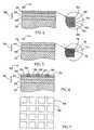
- FIG. 2shows one embodiment of a RCLED 30 according to the present invention that is fabricated using the method 10 , with the RCLED 30 shown at one of the intermediate steps in the method 10 .
- the RCLED 30comprises a silicon carbide substrate 32 that is used to anchor the epitaxial growth and has a first substrate surface 34 upon which the epitaxial growth nucleates. The first substrate surface 34 then becomes interface between silicon carbide substrate 32 and epitaxial device structure 36 .
- epitaxial structure 36comprises an n-type GaN layer 38 that is grown directly on silicon carbide substrate 32 and a p-type GaN layer 40 that is grown on top of n-type layer 38 .
- an active regioncan be included between the n-type and p-type layers.
- the RCLED 30further comprises a first mirror 42 that is deposited on the exposed surface of p-type epitaxial layer 32 .
- the RCLED 10is shown as it could appear after step 16 in method 10 of FIG. 1 .
- FIGS. 3-7show different embodiments of a RCLED according to the present invention as it could appear after step 16 in method 10 , with different mirror structures.
- FIG. 3shows an RCLED 50 , which has many of the same layers and the RCLED 30 . For those layers that are the same in this figure (and the figures that follow) the same reference numerals will be used and the features will not be reintroduced.
- the first mirror 52comprises a p-type metal mirror that can be made of silver, gold, rhodium, platinum, palladium or gold tin or combinations thereof.
- FIG. 4shows another embodiment of a RCLED 60 also having many of the same layers as RCLED 30 , but wherein the first mirror 62 is a DBR as described above in method 10 .
- DBR first mirror 62can be made of many different layer pairs having different thicknesses and different indexes of refraction, with the DBR first mirror 62 preferrably made of alternating dielectric layers of quarter wavelength thicknesses p-type silicon dioxide 64 and p-type titanium oxide 66 .
- Another embodiment of the DBR first mirror 62 according to the present inventioncomprises alternating dielectric layers of silicon dioxide and tantalum pentoxide.
- the contrast in indexes of refraction between device structure 36 made of GaN and layers 64 , 66 that form DBR first mirror 62is sufficient that the DBR first mirror 42 effectively reflects light with two to four alternating layer pairs, with a suitable number of alternating layer pairs being three, although a DBR first mirror 62 with fewer or more pairs can also be used.
- the thickness of these layerscorresponds to a quarter wavelength of light generated by the epitaxial device structure 36 when a bias is applied across the n-type and p-type layers 38 , 40 .
- FIG. 5shows another embodiment of an RCLED 70 having a first mirror 72 that is also a DBR made of p-type alternating pairs, with the alternating pairs made of an epitaxial material.
- the DBR first mirror 72comprising alternating pairs of p-type GaN 74 and p-type aluminum nitride 76 .
- aluminum alloy nitridecan be used instead of aluminum nitride.
- the index of refraction difference between epitaxial device structure 36 and the material that comprises DBR first mirror 72is such that the mirror 72 requires approximately eight to twelve layer pairs that are approximately a quarter wavelength thick, with a suitable number of layer pairs being ten. It is understood that the DBR will also work with fewer and more layer pairs.
- N-type Group-III nitride materialis a good conductor, so current typically spreads from its contact throughout the layer.
- P-type Group-III nitride materialconversely, is not a good conductor and current has difficulty spreading from a contact, particularly for larger devices.
- the metal mirror 52 in FIG. 3is a good conductor and will spread current from a contact throughout the p-type layer.
- the p-type DBR mirrors 62 , 72 described above in FIGS. 4 and 5do not effectively conduct electricity and have difficulty spreading current from a contact throughout the p-type layer.
- FIG. 6shows a RCLED 80 that combines the DBR p-type first mirror 82 with a metal mirror to enhance current spreading into the p-type layer 40 , with the first mirror 82 comprising a DBR 84 with a metal mesh 86 to spread current from a contact.
- the DBR 84is deposited on epitaxial structure 36 with a sufficient number of layers of appropriate thickness to be highly reflective. Channels are then opened in DBR 84 , usually by etching, which extend across the surface of the p-type layer 40 and are interconnected. These channels are then filled with metal mirror material to form the metal mesh 86 .
- FIG. 7is a top plan view of RCLED 80 showing the top surface of the DBR 84 and metal mesh 86 .
- the metal meshis shown as orthogonal and interconnected channels, although the mesh can have many different channel arrangements.
- FIG. 8shows an RCLED 90 after it is flip chip mounted on a submount pursuant to step 18 in the method 10 of FIG. 1 .
- the RCLEDhas many of the same features of RCLED 30 in FIG. 2 and, as with the FIGS. 3-7 , the same reference numerals are used for the same features.
- the RCLED 90can be any one of the RCLEDs described above in relation to FIGS. 2-7 and is flipped and adhered to a submount 92 by a bonding layer/material 94 with the mirror layer 96 adjacent to the submount 92 .
- the bonding layer/material 94comprises a submount epoxy material comprising silver tin eutectic.
- submount 92can be one of many structural members including silicon, silicon carbide, sapphire, glass or metals.
- RCLED 90can be placed in a reactive ion etch chamber having a reactive ion etch environment 98 that etches the substrate 32 at a high rate and etches the epitaxial layers at a slow rate.
- a reactive ion etch chamberhaving a reactive ion etch environment 98 that etches the substrate 32 at a high rate and etches the epitaxial layers at a slow rate.
- One embodiment of an etch environment according to the present inventioncomprises ions of nitrogen tri-fluoride, with the ions readily reducing and removing silicon carbide substrate 12 from the RCLED 30 until the surface of the epitaxial device structure 36 is reached, in this case the surface of the n-type epitaxial layer. Because the etch rate for silicon carbide is significantly greater than the etch rate of GaN, once all of silicon carbide substrate 12 has been removed, etching essentially ceases.
- FIG. 9shows the RCLED 90 of FIG. 8 with the substrate removed by the reactive ion etch after step 20 in the method 10 of FIG. 1 .
- the reactive ion etchin one embodiment can leave the top surface of semiconductor 30 in a condition ready to receive epitaxial growth or deposition of a metal for a second mirror.
- FIG. 10-15show different embodiments of an RCLED according to the present invention after step 22 of the method 10 in FIG. 1 , with the different RCLEDs comprising different types of second mirrors.
- FIG. 10shows one embodiment on the RCDLED 90 of FIG. 9 with a second mirror layer 100 on the newly exposed surface of the n-type layer 38 .
- the second mirror layer 100can be many different mirror types such as an n-type metal mirror, an n-type DBR or an n-type epitaxial Bragg reflector.
- the second mirror layer 100should have a lower reflectivity than the first mirror so that light exits the RCLED through the second mirror layer 100 .
- the first mirror layer 96can also be any of a metal layer, a p-type Bragg reflector DBR, or a p-type epitaxial mirror.
- Metallization layer 102cab be deposited on the exposed surface of second mirror n-type layer 100 and can be any of gold, silver, rhodium, palladium, platinum or gold tin for bonding.
- FIGS. 12-15show embodiments of a RCLED according to the present invention, each of which uses a different type of second mirror layer.
- FIG. 12shows a RCLED 110 according to the present invention utilizing an n-type metal for its second mirror layer 112 that can be made of the same material as mirror layer 52 described above and shown in FIG. 3 .
- FIG. 13shows a RCLED 120 according to the present invention utilizing an n-type DBR as its second mirror layer 122 .
- the DBR mirror layeris similar to the p-type DBR first mirror 62 shown in FIG. 4 and can be made of many different alternating pairs, but is preferably made of approximately three alternating pairs of a silicon dioxide layer 124 and a titanium dioxide 126 .
- FIG. 12shows a RCLED 110 according to the present invention utilizing an n-type metal for its second mirror layer 112 that can be made of the same material as mirror layer 52 described above and shown in FIG. 3 .
- FIG. 13shows a RCLED 120 according
- FIG. 14shows a RCLED 130 according to the present invention also utilizing a DBR as its second mirror layer 132 that is similar to the DBR first mirror layer 72 in FIG. 5 and comprises approximately ten pairs of n-type GaN 134 and n-type aluminum nitride 136 .
- FIGS. 15 and 16show an embodiment of an RCLED 140 according to the present invention wherein the second mirror layer 142 comprises an n-type DBR 144 with a metal mesh that is similar to the DBR 84 and metal mesh 86 described above and shown in FIGS. 6 and 7 , with the metal mesh 86 providing for good current spreading throughout the n-type epitaxial layer 38 .
- FIGS. 17-20show different embodiments of an RCLED according to the present invention that can be fabricated using the method 10 in FIG. 1 .
- the first mirror layercan be any of the metal mirror deposition, the p-type DBR, or the p-type epitaxial DBR.
- second mirror layercan be an n-type metal mirror, n-type DBR, or n-type epitaxial DBR.
- the selection of the second mirror layeris not constrained by the selection of the first mirror layer and vice versa.
- second mirror layercan be an n-type metal mirror when first mirror layer is a p-type DBR.
- FIG. 17shows one embodiment of an RCLED 150 according to the present invention that can be fabricated using the method 10 in FIG. 1 .
- RCLEDsrequire that the epitaxial structure 36 be thin, having a thickness of approximately one wavelength of the light being emitted by the structure 36 .
- the method 10provides for the fabrication of high quality Group-III nitride thin layers particularly adapted to RCLEDs.
- the first and second mirror layers 152 , 154can be any of those described above and the RCLED 150 also comprises a contact metal layer 156 on the second mirror layer 154 .
- the p-type layer 40can be contacted through the submount 92 such that the RCLED 150 emits light in response to a bias applied across the submount 92 and the contact metal layer 156 .
- FIG. 18shows one embodiment of a standard LED 160 according to the present invention, fabricated by the method 10 .
- the epitaxial structure 162has dimensions significantly larger than those of epitaxial structure 36 in the RCLEDs above, but the method 10 is equally adapted to the fabrication of devices with thicker layers.
- the LED 160also has an n-type contact 164 to provide a current to one of the oppositely doped layers in the structure 162 , with the other of the oppositely doped layers contacted through the submount 166 .
- FIG. 19shows an embodiment of LED 170 that has shaped side surfaces 172 , 174 and is roughened on its primary emitting surface 176 .
- the LED 170is typically shaped and roughened after the substrate removal method 10 is complete. Shaping and roughening the LED 170 increases the light extraction of the LED 170 by increasing the fraction of light that hits the surface and escapes to emit light from the device.
- FIG. 20shows an LED 180 that is similar to the LED 170 of FIG. 19 , but includes a zener diode 182 arranged between the submount 184 and the first mirror layer 186 .
- the zener diode 182is integrated into the submount 184 during submount fabrication and constrains the flow of current through the LED to one direction only.
- the LED shownalso has angled side surfaces 186 , 187 and a roughened emitting surface 188 .
- the submount 184is provided with the zener diode structure 182 , such that when the device is flip-chip mounted on the submount 184 the zener diode structure 182 is integral with the device.
- the resulting structureprovides high light extraction efficiency and high ESD rating. It is understood that the zener diode structure can be included in many different devices according to the present invention, including the different embodiments of the RCLEDs described above as well as vertical cavity surface emitting lasers and laser diodes.
- FIG. 21shows one embodiment of a VCSEL 190 according to the present invention fabricated by the method 10 .
- the first and second mirror layers surfaces 192 , 194are DBR mirrors.
- First DBR mirror 192is shown adhered to submount 92 by an epoxy epoxy/metallization 94 .
- the quantum well structure of this embodimentis a single quantum well having a lower cladding layer 196 that can be fabricated from aluminum indium gallium nitride.
- Quantum well 198is arranged above lower cladding layer 196 , and the quantum well 198 can be fabricated in one example from indium gallium nitride.
- Upper cladding layer 200is arranged above the quantum well 198 , such that the quantum well is sandwiched between the upper and lower cladding layers 200 , 196 .
- Upper cladding layer 200can be fabricated from aluminum gallium nitride.
- the second DBR mirror layer 194is deposited on top of upper cladding layer 200 .
- This structuremay be etched away to form isolated columns that can be round or rectangular. These isolated columns may then be further isolated by isolation epitaxial growth 202 .
- the isolation materialmay be ion implanted. Implantation may damage the crystalline structure between the cells which would require annealing.
- the deviceis capped off with metallization 204 .
- Metallizationuses isolation structures for support but since the isolation structure does not conduct electricity the metallizations must at least partially contact mirror 194 .
Landscapes
- Led Devices (AREA)
- Semiconductor Lasers (AREA)
- Led Device Packages (AREA)
Abstract
Description
- 1. Field of the Invention
- This invention relates to a method for fabricating a semiconductor device, and more particularly to method for fabricating thin film semiconductor devices wherein the growth substrate is removed by a reactive ion etch.
- 2. Description of the Related Art
- Improvements in the manufacturing of semiconductor materials in the Group-III nitride material system has focused interest on the development of GaN/AlGaN opto-electronic devices such as high efficiency blue, green and ultra-violet (UV) light emitting diodes (LED or LEDs) and lasers, and electronic devices such as high power microwave transistors. Some of the advantages of GaN is its 3.4 eV wide direct bandgap, high electron velocity (2×107cm/s), high breakdown field (2×10⁶V/cm) and the availability of heterostructures.
- Typical LEDs can comprise an active region sandwiched between a p-type doped layer and an n-type doped layer such that when a bias is applied across the doped layer electrons and holes are injected into the active region. The electrons and holes recombine in the active region to generate light omnidirectionally in an “emission sphere” with light radiating in all directions within the material that makes up the LED structure. Typical LEDs are efficient at generating light from the active region, but the light has difficulties emitting from the LED to the surroundings because of the differences in the indexes of refraction between the LED material and surroundings. In an LED having layers and regions of a typical thickness, only the photons formed in a cone about 20° wide in the direction of a surface exit the structure. The remainder of the light is trapped within the structure of the LED, and will eventually become absorbed into the semiconductor material. The light that is absorbed back into the LED material is lost to light generation, which reduces the overall emitting efficiency of the LED.
- Different methods have been developed for improving the light emitting efficiency of typical LEDs, some of which include using non-planar shaped LEDs and roughening the emission surface of an LED. Both of these approaches improve emitting efficiency by providing an LED surface that has different angles such that when light from the LED's active region reaches the surface with varying angles between the light and the surface. This increases the possibility that the light will be within the 20° cone when it reaches the surface such that it emits from the LED. If it is not within the 20° angle, the light is reflected at different angles, increasing the likelihood that the light will be within the cone the next time it reaches the surface.
- Emission efficiency is also enhanced by utilizing a resonant cavity structure in a resonant cavity LED (RCLED). RCLEDs are generally described in E. Fred Shubert,Light Emitting Diodes, Cambridge University Press, Pages 198-211 (2003). and typically comprise two oppositely doped epitaxial layers and mirrors on the oppositely doped layers such that the oppositely doped layers are sandwiched between the mirrors. One of the mirrors has reflectivity that is lower than the reflectivity of the other mirror so that light exits the RCLED through the lower reflectivity mirror. In other embodiments, an epitaxial active region can be included between the oppositely doped layers.
- RCLEDs typically comprise epitaxial layers that are much thinner than standard LEDs and a resonant cavity effect appears when the thickness of the epitaxial layers is approximately one wavelength of the light generated by the epitaxial layers. The light generated in the resonant cavity forms a standing wave such that all light emitted is emitted directionally. This directional light emission releases the photons in directions that are substantially normal to a plane formed by the diode junction.
- This structure allows RCLEDs to emit light intensity along the axis of the cavity (i.e. normal to the semiconductor surface) that is higher compared to conventional LEDs. The emission spectrum of RCLEDs has a higher spectral purity compared to conventional LEDs and the emission far-field pattern of RCLEDs is more directed compared to standard LEDs.
- When fabricating RCLEDs of certail material systems there are challenges in depositing the two mirrors on opposite sides of epitaxial layers. The oppositely doped layers (and active region) are typically formed on a substrate using known fabrication methods and devices, such as epitaxial growth in a metalorganic chemical vapor deposition (MOCVD) reactor. Once these layers have been deposited on the substrate the first of the two mirrors may be deposited on the top, most recently grown epitaxial surface, which is usually the p-type doped layer. Placing a mirror surface on the surface of the other doped, first grown layer is not so easy, because the surface is in contact with the growth surface of the substrate. The layers of RCLEDs are typically thin so it can be difficult to separate the substrate from the epitaxial layers so that the second mirror can be deposited. It may not be practical to deposit the mirror on the substrate and then grow the epitaxial layer because of the crystal lattice mismatch between the mirror material and epitaxial layers.
- One of the ways to deposit the second mirror on the epitaxial layers is to first remove the substrate. One technique for removing the substrate from epitaxial layers is described in U.S. Pat. No. 6,071,795 to W. Cheung et al. Thin films of GaN are epitaxially grown on a sapphire substrate and the substrate is then laser irradiated with a scanned beam at a wavelength at which sapphire is transparent but the GaN is absorbing (e.g. 248 mn wavelength). The intensity of the radiation, however, is low enough not to cause the irradiated area to separate. The separation process is performed after completion of the laser irradiation, such as by heating the structure to above the melting point of gallium. Another embodiment of the invention is described as growing a sacrificial material between the desired film and the growth substrate. The optical beam can then irradiate from the side of either the growth or acceptor substrate that is transparent to the optical beam.
- The difficulty with this approach is that it is particularly adapted to semiconductor devices grown on sapphire substrates. Group-III nitride devices are often grown on silicon carbide substrates and if the wavelength of the irradiating optical beam is high enough not to be absorbed by the silicon carbide, the wavelength can be too high to be absorbed by the GaN. One alternative to this is to find a wavelength of light that is transparent to silicon carbide that will excite GaN. The difference in bandgap between GaN and silicon carbide, however, is too narrow to allow reliable transmission through the silicon carbide while being absorbed by the GaN.
- One embodiment of a method for fabricating high light extraction photonic devices according to the present invention comprises growing an epitaxial semiconductor device structure on a substrate with the epitaxial semiconductor structure and substrate comprising an emitter adapted to emit light in response to a bias. Flip-chip mounting the epitaxial semiconductor structure and substrate on a submount such that the epitaxial semiconductor device structure is sandwiched between the submount and substrate. Etching the substrate off the epitaxial semiconductor device by utilizing an etch environment that etches the substrate is substantially faster than the epitaxial semiconductor structure.
- A method for fabricating high light extraction photonic devices according to the present invention comprises growing an epitaxial semiconductor structure on a substrate and depositing a first mirror layer on the epitaxial semiconductor structure such that the epitaxial semiconductor structure is sandwiched between the first mirror layer and the substrate. The substrate is then removed from the epitaxial structure by introducing an etch environment to the substrate and a second mirror layer is deposited on the epitaxial semiconductor structure such that the epitaxial semiconductor structure is sandwiched between the first and second mirror layers.
- One embodiment of resonant cavity light emitting diode (RCLED) according to the present invention comprises a thin film epitaxial semiconductor structure and a fist mirror layer on one surface of the eptaxial semiconductor structure. A second mirror layer is included on another surface of said epitaxial semiconductor structure such that said epitaxial semiconductor structure is sandwiched between the first and second mirrors, the second mirror layer being less reflective than the first mirror layer. A submount is also included, said epitaxial semiconductor structure with its first and second mirrors mounted on the submount, the first mirror layer being adjacent to the submount and the second mirror layer being the primiary emitting surface.
- A method for removing a silicon carbide substrate from a Group-III nitride epitaxial semiconductor material, comprising growing a Group-III nitride epitaxial semiconductor material on a silicon carbide substrate. An etch environment is introduced to the silicon carbide substrate, the etch environment etching silicon carbide faster than the Group-III nitride epitaxial material such that the etching substantially stops after the silicon carbide is etched off.
- These and other features and advantages of the invention will be apparent to those skilled in the art from the following detailed description, taken together with the accompanying drawings, in which:
FIG. 1 is a flow diagram for one embodiment of a fabrication method according to the present invention;FIG. 2 is a sectional view of one embodiment of a semiconductor device according to the present invention at one of the intermediate steps of the method inFIG. 1 ;FIG. 3 is a sectional view of another embodiment of a semiconductor device according to the present invention at one of the intermediate steps of the method inFIG. 1 ;FIG. 4 is a sectional view of another embodiment of a semiconductor device according to the present invention at one of the intermediate steps of the method inFIG. 1 ;FIG. 5 is a sectional view of another embodiment of a semiconductor device according to the present invention at one of the intermediate steps of the method inFIG. 1 ;FIG. 6 is a sectional view of still another embodiment of a semiconductor device according to the present invention at one of the intermediate steps of the method inFIG. 1 ;FIG. 7 is a plan view of the semiconductor device inFIG. 6 ;FIG. 8 is a sectional view of one embodiment of a semiconductor device according to the present invention at a flip chip step of the method inFIG. 1 .FIG. 9 is sectional view of the semiconductor device inFIG. 8 after etching off the substrate according to the method ofFIG. 1 ;FIG. 10 is a sectional view of one embodiment of a semiconductor device according to the present invention at another intermediate step of the method inFIG. 1 ;FIG. 11 is a sectional view of another embodiment of a semiconductor device according to the present invention at another step of the method inFIG. 1 ;FIG. 12 is a sectional view of another embodiment of a semiconductor device according to the present invention at another step of the method inFIG. 1 ;FIG. 13 is a sectional view of another embodiment of a semiconductor device according to the present invention at another step of the method inFIG. 1 ;FIG. 14 is a sectional view of another embodiment of a semiconductor device according to the present invention at another step of the method inFIG. 1 ;FIG. 15 is a sectional view of another embodiment of a semiconductor device according to the present invention at another step of the method inFIG. 1 ;FIG. 16 is a plan view of the semiconductor device inFIG. 15 ;FIG. 17 is a sectional view of one embodiment of a semiconductor device according to the present invention;FIG. 18 is a sectional view of another embodiment of a semiconductor device according to the present invention;FIG. 19 is a sectional view of another embodiment of a semiconductor device according to the present invention;FIG. 20 is a sectional view of another embodiment of a semiconductor device according to the present invention; andFIG. 21 is a sectional view of still another embodiment of a semiconductor device according to the present invention.FIG. 1 shows one embodiment of amethod 10 according to the present invention for fabricating Group-III nitride semiconductors, with themethod 10 being particularly adapted for fabricating thin film Group-III nitride semiconductor devices. Instep 12, a substrate is provided that can be made of many different materials, with a preferred material being silicon carbide. SiC is a suitable material for use with Group-III nitride materials, such as GaN, because it has a closer crystal lattice match to Group III nitrides GaN, which generally results in Group III nitride films of high quality. Silicon carbide also has high thermal conductivity so that the total output power of Group III nitride devices on silicon carbide is not limited by the thermal dissipation of the substrate (as is the case with some devices formed on sapphire). SiC substrates are available from Cree Research, Inc., of Durham, N.C. and methods for producing them are set forth in the scientific literature as well as in a U.S. Pat. Nos. Re. 34,861; 4,946,547; and 5,200,022.- In
step 14 Group-III nitride epitaxial layer(s) are grown on the substrate using any of the known semiconductor fabrication processes such as molecular beam epitaxy (MBE) or metal organic chemical vapor deposition (MOCVD). Depending on the type of device being fabricated, anoptional step 16 is included that comprises depositing a first mirror layer on the surface of the epitaxial layers opposite the substrate. As will be understood by the discussion below, if a light emitting diode (LED) is being fabricated, this mirror helps increase the useful light extraction of the LED, and if an RCLED is being fabricated this mirror is necessary to generate the resonant cavity effect. Different mirrors can be used, such as metal mirrors made of materials such as silver, gold, rhodium, platinum, palladium, gold tin or combinations thereof, which can be deposited on the surface using a conventional method such as sputtering. Alternatively, the mirror can be a distributed Bragg reflector (DBR) which generally comprises multiple pairs of two materials having different refractive indexes. As a result of the difference in the refractive index, Fresnel reflection occurs at each of the interfaces. The reflection at each may not be total, but because of the number of interfaces and the thicknesses of the different layers, the reflected waves constructively interfere so that the DBR provides good reflectivity. Depending on the type of material used for the DBR, it can be deposited on the top surface using the same method used to fabricate the epitaxial layer, usually MBE or MOCVD. - In
step 18, the substrate, with its epitaxial layers and first mirror layer, is flip-chip mounted to a submount such that the top surface of the epitaxial layers, or the mirror, as the case may be, is adjacent to the submount. The surface of the eptitaxial layer or mirror layer can be bonded to the substrate using many known materials, one example being silver tin eutectic. The submount can be one of a single construction or can include a number of different structural members, and can be made of different materials such as silicon, silicon carbide, sapphire, glass or metals. The submount can also include electronic components to drive the device that comprises the Group-III epitaxial layers. - In
step 20, the substrate is etched off of the eptixial layers with the preferred etch being a composition that selectively removes the substrate at a high etch rate while etching the eptitaxial layers at a very low etch rate. In one embodiment according to the present invention, the etch material can be nitrogen tri fluoride, which etches silicon carbide at a rate many times faster than in etches Group-III nitride epitaxial layers. Ions of nitrogen tri fluoride readily remove silicon carbide down to its interface with the Group-III nitride materials. Once the silicon carbide is removed, etching essentially stops because the etch rate of the epitaxial layers is so slow. - Depending on the device being fabricated
alternate step 22 can be included wherein a mirror can be deposited on the surface of the epitaxial layers that is revealed by the etching process. This step is usually included when fabricating a resonant cavity LED (RCLED), solid state laser, or vertical-cavity surface-emitting laser (VCSEL). - The
method 10 can be used in fabricating many different semiconductor devices having epitaxial layers made of many different materials with many different thicknesses. Themethod 10 is particularly adapted to growing high quality thin film Group-III nitride layers used in RCLEDs, which mirrors on the opposing sides of the thin films. When forming a Group-III nitride RCLED t is impractical to provide a mirror on the interface between the SiC substrate epitaxial layer because mirrors either have no recognizable monocrystalline structure or they are monocrystalline with a significantly different sized crystal lattice than that formed by epitaxial layers. As a result, it is difficult to fabricate high quality thin Group-III nitride layers on a mirror surface because of the mismatch in crystal structures. - SiC substrates, on the other hand, have a good crystal lattice match to Group III nitrides which generally results in thin Group III nitride layers of high quality. The thin epitaxial layers can require support during processing steps that follow growth on the substrate, and the
method 10 allows for the first mirror to be deposited on the one surface of the epitaxial layers while the substrate is in place and supports the thin layers. The device is then flip chipped on a submount with the first mirror between the submount and layers. The submount provides additional support while the substrate is etched off and the second mirror is deposited. By providing this support through processing, high quality thin film devices can be fabricated in the Group-III nitride material system. FIG. 2 shows one embodiment of aRCLED 30 according to the present invention that is fabricated using themethod 10, with theRCLED 30 shown at one of the intermediate steps in themethod 10. TheRCLED 30 comprises asilicon carbide substrate 32 that is used to anchor the epitaxial growth and has afirst substrate surface 34 upon which the epitaxial growth nucleates. Thefirst substrate surface 34 then becomes interface betweensilicon carbide substrate 32 andepitaxial device structure 36. In this embodimentepitaxial structure 36 comprises an n-type GaN layer 38 that is grown directly onsilicon carbide substrate 32 and a p-type GaN layer 40 that is grown on top of n-type layer 38. In other embodiments, an active region can be included between the n-type and p-type layers. TheRCLED 30 further comprises afirst mirror 42 that is deposited on the exposed surface of p-type epitaxial layer 32. TheRCLED 10 is shown as it could appear afterstep 16 inmethod 10 ofFIG. 1 .FIGS. 3-7 show different embodiments of a RCLED according to the present invention as it could appear afterstep 16 inmethod 10, with different mirror structures.FIG. 3 shows anRCLED 50, which has many of the same layers and theRCLED 30. For those layers that are the same in this figure (and the figures that follow) the same reference numerals will be used and the features will not be reintroduced. InRCLED 50 thefirst mirror 52 comprises a p-type metal mirror that can be made of silver, gold, rhodium, platinum, palladium or gold tin or combinations thereof.FIG. 4 shows another embodiment of aRCLED 60 also having many of the same layers asRCLED 30, but wherein thefirst mirror 62 is a DBR as described above inmethod 10. DBRfirst mirror 62 can be made of many different layer pairs having different thicknesses and different indexes of refraction, with the DBRfirst mirror 62 preferrably made of alternating dielectric layers of quarter wavelength thicknesses p-type silicon dioxide 64 and p-type titanium oxide 66. Another embodiment of the DBRfirst mirror 62 according to the present invention comprises alternating dielectric layers of silicon dioxide and tantalum pentoxide. The contrast in indexes of refraction betweendevice structure 36 made of GaN and layers64,66 that form DBRfirst mirror 62 is sufficient that the DBRfirst mirror 42 effectively reflects light with two to four alternating layer pairs, with a suitable number of alternating layer pairs being three, although a DBRfirst mirror 62 with fewer or more pairs can also be used. The thickness of these layers corresponds to a quarter wavelength of light generated by theepitaxial device structure 36 when a bias is applied across the n-type and p-type layers FIG. 5 shows another embodiment of anRCLED 70 having afirst mirror 72 that is also a DBR made of p-type alternating pairs, with the alternating pairs made of an epitaxial material. Many different alternating pairs can be used, with the DBRfirst mirror 72 comprising alternating pairs of p-type GaN 74 and p-type aluminum nitride 76. In other embodiments of the DBRfirst mirror 72 aluminum alloy nitride can be used instead of aluminum nitride. The index of refraction difference betweenepitaxial device structure 36 and the material that comprises DBRfirst mirror 72 is such that themirror 72 requires approximately eight to twelve layer pairs that are approximately a quarter wavelength thick, with a suitable number of layer pairs being ten. It is understood that the DBR will also work with fewer and more layer pairs.- One concern when fabricating Group-III nitride LEDs is ensuring that current spreads from the contacts throughout the n-type and p-type layers such that the LED uniformly emits light. N-type Group-III nitride material is a good conductor, so current typically spreads from its contact throughout the layer. P-type Group-III nitride material, conversely, is not a good conductor and current has difficulty spreading from a contact, particularly for larger devices. The
metal mirror 52 inFIG. 3 is a good conductor and will spread current from a contact throughout the p-type layer. The p-type DBR mirrors62,72 described above inFIGS. 4 and 5 , however, do not effectively conduct electricity and have difficulty spreading current from a contact throughout the p-type layer. FIG. 6 shows aRCLED 80 that combines the DBR p-typefirst mirror 82 with a metal mirror to enhance current spreading into the p-type layer 40, with thefirst mirror 82 comprising aDBR 84 with ametal mesh 86 to spread current from a contact. TheDBR 84 is deposited onepitaxial structure 36 with a sufficient number of layers of appropriate thickness to be highly reflective. Channels are then opened inDBR 84, usually by etching, which extend across the surface of the p-type layer 40 and are interconnected. These channels are then filled with metal mirror material to form themetal mesh 86.DBR 84 has a higher reflectivity ofmetal 86, but the combination ofmetal 86 andDBR 84 comprises a layer with sufficient reflectivity and good current spreading.FIG. 7 is a top plan view ofRCLED 80 showing the top surface of theDBR 84 andmetal mesh 86. The metal mesh is shown as orthogonal and interconnected channels, although the mesh can have many different channel arrangements.FIG. 8 shows anRCLED 90 after it is flip chip mounted on a submount pursuant to step18 in themethod 10 ofFIG. 1 . The RCLED has many of the same features ofRCLED 30 inFIG. 2 and, as with theFIGS. 3-7 , the same reference numerals are used for the same features. TheRCLED 90 can be any one of the RCLEDs described above in relation toFIGS. 2-7 and is flipped and adhered to asubmount 92 by a bonding layer/material 94 with themirror layer 96 adjacent to thesubmount 92. In one embodiment according to the invention the bonding layer/material 94 comprises a submount epoxy material comprising silver tin eutectic. As described above,submount 92 can be one of many structural members including silicon, silicon carbide, sapphire, glass or metals.- Once the
RCLED 90 is bonded to submount92 thesubstrate 32 can be removed from thestructure 36, preferably by etching. TheRCLED 90 with its submount92 (hereinafter referred to as “RCLED 90”) can be placed in a reactive ion etch chamber having a reactiveion etch environment 98 that etches thesubstrate 32 at a high rate and etches the epitaxial layers at a slow rate. One embodiment of an etch environment according to the present invention comprises ions of nitrogen tri-fluoride, with the ions readily reducing and removingsilicon carbide substrate 12 from theRCLED 30 until the surface of theepitaxial device structure 36 is reached, in this case the surface of the n-type epitaxial layer. Because the etch rate for silicon carbide is significantly greater than the etch rate of GaN, once all ofsilicon carbide substrate 12 has been removed, etching essentially ceases. FIG. 9 shows theRCLED 90 ofFIG. 8 with the substrate removed by the reactive ion etch afterstep 20 in themethod 10 ofFIG. 1 . The reactive ion etch in one embodiment can leave the top surface ofsemiconductor 30 in a condition ready to receive epitaxial growth or deposition of a metal for a second mirror.FIG. 10-15 show different embodiments of an RCLED according to the present invention afterstep 22 of themethod 10 inFIG. 1 , with the different RCLEDs comprising different types of second mirrors.FIG. 10 shows one embodiment on theRCDLED 90 ofFIG. 9 with asecond mirror layer 100 on the newly exposed surface of the n-type layer 38. Thesecond mirror layer 100 can be many different mirror types such as an n-type metal mirror, an n-type DBR or an n-type epitaxial Bragg reflector. Thesecond mirror layer 100, however, should have a lower reflectivity than the first mirror so that light exits the RCLED through thesecond mirror layer 100. Thefirst mirror layer 96 can also be any of a metal layer, a p-type Bragg reflector DBR, or a p-type epitaxial mirror.Metallization layer 102 cab be deposited on the exposed surface of second mirror n-type layer 100 and can be any of gold, silver, rhodium, palladium, platinum or gold tin for bonding.FIGS. 12-15 show embodiments of a RCLED according to the present invention, each of which uses a different type of second mirror layer.FIG. 12 shows aRCLED 110 according to the present invention utilizing an n-type metal for itssecond mirror layer 112 that can be made of the same material asmirror layer 52 described above and shown inFIG. 3 .FIG. 13 shows aRCLED 120 according to the present invention utilizing an n-type DBR as itssecond mirror layer 122. The DBR mirror layer is similar to the p-type DBRfirst mirror 62 shown inFIG. 4 and can be made of many different alternating pairs, but is preferably made of approximately three alternating pairs of asilicon dioxide layer 124 and atitanium dioxide 126.FIG. 14 shows aRCLED 130 according to the present invention also utilizing a DBR as itssecond mirror layer 132 that is similar to the DBRfirst mirror layer 72 inFIG. 5 and comprises approximately ten pairs of n-type GaN 134 and n-type aluminum nitride 136.- Although current spreading is not so much of a concern for n-type Group-III nitride materials, current spreading structure can also be included in the second mirror layer.
FIGS. 15 and 16 show an embodiment of anRCLED 140 according to the present invention wherein thesecond mirror layer 142 comprises an n-type DBR 144 with a metal mesh that is similar to theDBR 84 andmetal mesh 86 described above and shown inFIGS. 6 and 7 , with themetal mesh 86 providing for good current spreading throughout the n-type epitaxial layer 38. FIGS. 17-20 show different embodiments of an RCLED according to the present invention that can be fabricated using themethod 10 inFIG. 1 . In each of the RCLEDs shown, the first mirror layer can be any of the metal mirror deposition, the p-type DBR, or the p-type epitaxial DBR. Similarly, in each of the RCLEDs that second mirror layer can be an n-type metal mirror, n-type DBR, or n-type epitaxial DBR. In these figures the selection of the second mirror layer is not constrained by the selection of the first mirror layer and vice versa. For example, second mirror layer can be an n-type metal mirror when first mirror layer is a p-type DBR.FIG. 17 shows one embodiment of anRCLED 150 according to the present invention that can be fabricated using themethod 10 inFIG. 1 . As described above, RCLEDs require that theepitaxial structure 36 be thin, having a thickness of approximately one wavelength of the light being emitted by thestructure 36. Themethod 10 provides for the fabrication of high quality Group-III nitride thin layers particularly adapted to RCLEDs. The first and second mirror layers152,154 can be any of those described above and theRCLED 150 also comprises acontact metal layer 156 on thesecond mirror layer 154. The p-type layer 40 can be contacted through thesubmount 92 such that theRCLED 150 emits light in response to a bias applied across thesubmount 92 and thecontact metal layer 156.- The
method 10 inFIG. 1 can also be used in the fabrication of devices having epitaxial layers that are thicker than those in RCLEDS.FIG. 18 shows one embodiment of astandard LED 160 according to the present invention, fabricated by themethod 10. Theepitaxial structure 162 has dimensions significantly larger than those ofepitaxial structure 36 in the RCLEDs above, but themethod 10 is equally adapted to the fabrication of devices with thicker layers. TheLED 160 also has an n-type contact 164 to provide a current to one of the oppositely doped layers in thestructure 162, with the other of the oppositely doped layers contacted through thesubmount 166. - The
method 10 can also be used in fabricating epitaxial devices that have other features to enhance light extraction.FIG. 19 shows an embodiment ofLED 170 that has shaped side surfaces172,174 and is roughened on its primary emittingsurface 176. TheLED 170 is typically shaped and roughened after thesubstrate removal method 10 is complete. Shaping and roughening theLED 170 increases the light extraction of theLED 170 by increasing the fraction of light that hits the surface and escapes to emit light from the device. - All of the devices described herein can also be fabricated with additional layers and features, one of them being a structure to protect the device from eletro-static discharge (ESD).
FIG. 20 shows anLED 180 that is similar to theLED 170 ofFIG. 19 , but includes azener diode 182 arranged between the submount184 and thefirst mirror layer 186. Thezener diode 182 is integrated into thesubmount 184 during submount fabrication and constrains the flow of current through the LED to one direction only. The LED shown also has angled side surfaces186,187 and a roughened emittingsurface 188. When fabricatingLED 180 using themethod 10, thesubmount 184 is provided with thezener diode structure 182, such that when the device is flip-chip mounted on thesubmount 184 thezener diode structure 182 is integral with the device. The resulting structure provides high light extraction efficiency and high ESD rating. It is understood that the zener diode structure can be included in many different devices according to the present invention, including the different embodiments of the RCLEDs described above as well as vertical cavity surface emitting lasers and laser diodes. - The
method 10 can also be used to fabricate other devises such as a vertical cavity surface emitting laser (VCSEL).FIG. 21 shows one embodiment of aVCSEL 190 according to the present invention fabricated by themethod 10. In this embodiment the first and second mirror layers surfaces192,194 are DBR mirrors.First DBR mirror 192 is shown adhered to submount92 by an epoxy epoxy/metallization 94. The quantum well structure of this embodiment is a single quantum well having alower cladding layer 196 that can be fabricated from aluminum indium gallium nitride. Quantum well198 is arranged abovelower cladding layer 196, and the quantum well198 can be fabricated in one example from indium gallium nitride.Upper cladding layer 200 is arranged above the quantum well198, such that the quantum well is sandwiched between the upper and lower cladding layers200,196.Upper cladding layer 200 can be fabricated from aluminum gallium nitride. - The second
DBR mirror layer 194 is deposited on top ofupper cladding layer 200. This structure may be etched away to form isolated columns that can be round or rectangular. These isolated columns may then be further isolated by isolationepitaxial growth 202. In one embodiment the isolation material may be ion implanted. Implantation may damage the crystalline structure between the cells which would require annealing. The device is capped off withmetallization 204. Metallization uses isolation structures for support but since the isolation structure does not conduct electricity the metallizations must at least partially contactmirror 194. - Although the present invention has been described in considerable detail with reference to certain preferred configurations thereof, other versions are possible. The methods according to the present invention can be used to fabricate many different devices and the devices described above can have many different layer arrangements. Therefore, the spirit and scope of the appended claims should not be limited to the preferred versions in the specification.
Claims (48)
Priority Applications (10)
| Application Number | Priority Date | Filing Date | Title |
|---|---|---|---|
| US10/848,937US7332365B2 (en) | 2004-05-18 | 2004-05-18 | Method for fabricating group-III nitride devices and devices fabricated using method |
| PCT/US2005/016987WO2005117152A1 (en) | 2004-05-18 | 2005-05-17 | Method for fabricating group iii nitride devices and devices fabricated using method |
| JP2007527328AJP5468203B2 (en) | 2004-05-18 | 2005-05-17 | Method of manufacturing a group 3 nitride device and device manufactured using the method |
| KR1020067025952AKR20070013324A (en) | 2004-05-18 | 2005-05-17 | Method for manufacturing group III nitride device and device manufactured using the method |
| CA002564995ACA2564995A1 (en) | 2004-05-18 | 2005-05-17 | Method for fabricating group iii nitride devices and devices fabricated using method |
| CNA2005800158033ACN1957481A (en) | 2004-05-18 | 2005-05-17 | Method for manufacturing group-III nitride device and device manufactured using the method |
| EP05751127.1AEP1763900B1 (en) | 2004-05-18 | 2005-05-17 | Method for fabricating group iii nitride devices |
| TW094116021ATWI390759B (en) | 2004-05-18 | 2005-05-18 | Method for manufacturing a group III nitride device and device manufactured using the same |
| US11/343,180US7791061B2 (en) | 2004-05-18 | 2006-01-30 | External extraction light emitting diode based upon crystallographic faceted surfaces |
| US12/834,608US8357923B2 (en) | 2004-05-18 | 2010-07-12 | External extraction light emitting diode based upon crystallographic faceted surfaces |
Applications Claiming Priority (1)
| Application Number | Priority Date | Filing Date | Title |
|---|---|---|---|
| US10/848,937US7332365B2 (en) | 2004-05-18 | 2004-05-18 | Method for fabricating group-III nitride devices and devices fabricated using method |
Related Child Applications (1)
| Application Number | Title | Priority Date | Filing Date |
|---|---|---|---|
| US11/343,180Continuation-In-PartUS7791061B2 (en) | 2004-05-18 | 2006-01-30 | External extraction light emitting diode based upon crystallographic faceted surfaces |
Publications (2)
| Publication Number | Publication Date |
|---|---|
| US20060049411A1true US20060049411A1 (en) | 2006-03-09 |
| US7332365B2 US7332365B2 (en) | 2008-02-19 |
Family
ID=34970241
Family Applications (1)
| Application Number | Title | Priority Date | Filing Date |
|---|---|---|---|
| US10/848,937Expired - LifetimeUS7332365B2 (en) | 2004-05-18 | 2004-05-18 | Method for fabricating group-III nitride devices and devices fabricated using method |
Country Status (8)
| Country | Link |
|---|---|
| US (1) | US7332365B2 (en) |
| EP (1) | EP1763900B1 (en) |
| JP (1) | JP5468203B2 (en) |
| KR (1) | KR20070013324A (en) |
| CN (1) | CN1957481A (en) |
| CA (1) | CA2564995A1 (en) |
| TW (1) | TWI390759B (en) |
| WO (1) | WO2005117152A1 (en) |
Cited By (25)
| Publication number | Priority date | Publication date | Assignee | Title |
|---|---|---|---|---|
| US20050271107A1 (en)* | 2004-06-08 | 2005-12-08 | Fuji Xerox Co., Ltd. | Semiconductor laser apparatus and manufacturing method thereof |
| US20060154455A1 (en)* | 2002-12-04 | 2006-07-13 | Emcore Corporation | Gallium nitride-based devices and manufacturing process |
| US20060186418A1 (en)* | 2004-05-18 | 2006-08-24 | Edmond John A | External extraction light emitting diode based upon crystallographic faceted surfaces |
| US20080064133A1 (en)* | 2004-08-11 | 2008-03-13 | Samsung Electro-Mechanics., Ltd | Nitride semiconductor light emitting diode and method of manufacturing the same |
| US20080121923A1 (en)* | 2006-09-26 | 2008-05-29 | Osram Opto Semiconductors Gmbh | Method for producing an optoelectronic component, and an optoelectronic component |
| WO2008073384A1 (en)* | 2006-12-11 | 2008-06-19 | The Regents Of University Of California | Non-polar and semi-polar light emitting devices |
| US20080210971A1 (en)* | 2006-06-30 | 2008-09-04 | Matthew Donofrio | Nickel tin bonding system with barrier layer for semiconductor wafers and devices |
| US20080251800A1 (en)* | 2007-04-11 | 2008-10-16 | Bergmann Michael J | Undoped and Unintentionally Doped Buffer Structures |
| EP2113949A2 (en) | 2008-05-02 | 2009-11-04 | Cree, Inc. | Encapsulation for phosphor-converted white light emitting diode |
| US20090272994A1 (en)* | 2008-04-30 | 2009-11-05 | Lim Woo Sik | Semiconductor light emitting device |
| US7855459B2 (en) | 2006-09-22 | 2010-12-21 | Cree, Inc. | Modified gold-tin system with increased melting temperature for wafer bonding |
| US20110049546A1 (en)* | 2009-09-02 | 2011-03-03 | Cree, Inc. | high reflectivity mirrors and method for making same |
| US20110096548A1 (en)* | 2009-10-27 | 2011-04-28 | Paul Kenneth Pickard | Hybrid reflector system for lighting device |
| US8643195B2 (en) | 2006-06-30 | 2014-02-04 | Cree, Inc. | Nickel tin bonding system for semiconductor wafers and devices |
| US8877524B2 (en) | 2008-03-31 | 2014-11-04 | Cree, Inc. | Emission tuning methods and devices fabricated utilizing methods |
| US8896008B2 (en) | 2013-04-23 | 2014-11-25 | Cree, Inc. | Light emitting diodes having group III nitride surface features defined by a mask and crystal planes |
| US8956896B2 (en) | 2006-12-11 | 2015-02-17 | The Regents Of The University Of California | Metalorganic chemical vapor deposition (MOCVD) growth of high performance non-polar III-nitride optical devices |
| US9012938B2 (en) | 2010-04-09 | 2015-04-21 | Cree, Inc. | High reflective substrate of light emitting devices with improved light output |
| US9105824B2 (en) | 2010-04-09 | 2015-08-11 | Cree, Inc. | High reflective board or substrate for LEDs |
| US20160118538A1 (en)* | 2006-07-28 | 2016-04-28 | Epistar Corporation | Light-emitting device having a patterned substrate and the method thereof |
| US9461201B2 (en) | 2007-11-14 | 2016-10-04 | Cree, Inc. | Light emitting diode dielectric mirror |
| US9728676B2 (en) | 2011-06-24 | 2017-08-08 | Cree, Inc. | High voltage monolithic LED chip |
| US10186644B2 (en) | 2011-06-24 | 2019-01-22 | Cree, Inc. | Self-aligned floating mirror for contact vias |
| WO2019125306A1 (en)* | 2017-12-21 | 2019-06-27 | Agency For Science, Technology And Research | Optical device and method of forming the same |
| US10658546B2 (en) | 2015-01-21 | 2020-05-19 | Cree, Inc. | High efficiency LEDs and methods of manufacturing |
Families Citing this family (39)
| Publication number | Priority date | Publication date | Assignee | Title |
|---|---|---|---|---|
| US8482663B2 (en)* | 2004-06-30 | 2013-07-09 | Osram Opto Semiconductors Gmbh | Light-emitting diode arrangement, optical recording device and method for the pulsed operation of at least one light-emitting diode |
| KR100682877B1 (en)* | 2005-07-12 | 2007-02-15 | 삼성전기주식회사 | Light emitting diode and manufacturing method |
| US20070019699A1 (en)* | 2005-07-22 | 2007-01-25 | Robbins Virginia M | Light emitting device and method of manufacture |
| US7772604B2 (en) | 2006-01-05 | 2010-08-10 | Illumitex | Separate optical device for directing light from an LED |
| US7915624B2 (en) | 2006-08-06 | 2011-03-29 | Lightwave Photonics, Inc. | III-nitride light-emitting devices with one or more resonance reflectors and reflective engineered growth templates for such devices, and methods |
| WO2008042351A2 (en)* | 2006-10-02 | 2008-04-10 | Illumitex, Inc. | Led system and method |
| US8941141B2 (en)* | 2006-10-17 | 2015-01-27 | Epistar Corporation | Light-emitting device |
| KR100826412B1 (en)* | 2006-11-03 | 2008-04-29 | 삼성전기주식회사 | Nitride semiconductor light emitting device and manufacturing method |
| US7928471B2 (en)* | 2006-12-04 | 2011-04-19 | The United States Of America As Represented By The Secretary Of The Navy | Group III-nitride growth on silicon or silicon germanium substrates and method and devices therefor |
| US7915629B2 (en) | 2008-12-08 | 2011-03-29 | Cree, Inc. | Composite high reflectivity layer |
| US8368100B2 (en) | 2007-11-14 | 2013-02-05 | Cree, Inc. | Semiconductor light emitting diodes having reflective structures and methods of fabricating same |
| DE102008006988A1 (en)* | 2008-01-31 | 2009-08-06 | Osram Opto Semiconductors Gmbh | Optoelectronic component and method for producing an optoelectronic component |
| JP2011512037A (en)* | 2008-02-08 | 2011-04-14 | イルミテックス, インコーポレイテッド | System and method for emitter layer shaping |
| WO2009108733A2 (en) | 2008-02-25 | 2009-09-03 | Lightwave Photonics, Inc. | Current-injecting/tunneling light-emitting device and method |
| KR101308130B1 (en) | 2008-03-25 | 2013-09-12 | 서울옵토디바이스주식회사 | Light emitting device and method for fabricating the same |
| DE102008050538B4 (en) | 2008-06-06 | 2022-10-06 | OSRAM Opto Semiconductors Gesellschaft mit beschränkter Haftung | Optoelectronic component and method for its production |
| US8017963B2 (en) | 2008-12-08 | 2011-09-13 | Cree, Inc. | Light emitting diode with a dielectric mirror having a lateral configuration |
| TW201034256A (en)* | 2008-12-11 | 2010-09-16 | Illumitex Inc | Systems and methods for packaging light-emitting diode devices |
| US8529102B2 (en) | 2009-04-06 | 2013-09-10 | Cree, Inc. | Reflector system for lighting device |
| US8096671B1 (en) | 2009-04-06 | 2012-01-17 | Nmera, Llc | Light emitting diode illumination system |
| US8449128B2 (en)* | 2009-08-20 | 2013-05-28 | Illumitex, Inc. | System and method for a lens and phosphor layer |
| US8585253B2 (en) | 2009-08-20 | 2013-11-19 | Illumitex, Inc. | System and method for color mixing lens array |
| KR101100681B1 (en)* | 2009-09-10 | 2012-01-03 | 주식회사 에피밸리 | Semiconductor light emitting device |
| KR20110133241A (en) | 2010-06-04 | 2011-12-12 | 서울옵토디바이스주식회사 | Light emitting diode manufacturing method |
| US8764224B2 (en) | 2010-08-12 | 2014-07-01 | Cree, Inc. | Luminaire with distributed LED sources |
| US8556469B2 (en) | 2010-12-06 | 2013-10-15 | Cree, Inc. | High efficiency total internal reflection optic for solid state lighting luminaires |
| US8680556B2 (en) | 2011-03-24 | 2014-03-25 | Cree, Inc. | Composite high reflectivity layer |
| CN102738332A (en)* | 2011-04-13 | 2012-10-17 | 展晶科技(深圳)有限公司 | Light emitting diode epitaxial structure and manufacture method thereof |
| US8686429B2 (en) | 2011-06-24 | 2014-04-01 | Cree, Inc. | LED structure with enhanced mirror reflectivity |
| TWI495163B (en)* | 2011-12-09 | 2015-08-01 | Chunghwa Telecom Co Ltd | A method for manufacturing a resonant cavity light emitting diode |
| US20140008660A1 (en)* | 2012-03-14 | 2014-01-09 | Lightwave Photonics, Inc. | Materials, structures, and methods for optical and electrical iii-nitride semiconductor devices |
| TW201340405A (en)* | 2012-03-30 | 2013-10-01 | Lextar Electronics Corp | Light-emitting diode |
| JP6500342B2 (en)* | 2013-04-27 | 2019-04-17 | 日亜化学工業株式会社 | Method of manufacturing semiconductor laser device and method of manufacturing submount |
| KR102380825B1 (en)* | 2015-05-29 | 2022-04-01 | 삼성전자주식회사 | Semiconductor light emitting diode chip and light emitting device having the same |
| US10263144B2 (en) | 2015-10-16 | 2019-04-16 | Robbie J. Jorgenson | System and method for light-emitting devices on lattice-matched metal substrates |
| KR102383837B1 (en) | 2016-05-26 | 2022-04-07 | 로비 조젠슨 | Group 3A nitride growth system and method |
| TWI781742B (en) | 2021-08-26 | 2022-10-21 | 隆達電子股份有限公司 | Light-emitting diode |
| DE102022120161A1 (en)* | 2022-08-10 | 2024-02-15 | Ams-Osram International Gmbh | OPTOELECTRONIC SEMICONDUCTOR COMPONENT WITH EPITACTICALLY GROWN LAYER AND METHOD FOR PRODUCING THE OPTOELECTRONIC SEMICONDUCTOR COMPONENT |
| CN117913017B (en)* | 2024-01-19 | 2024-10-22 | 江苏宜兴德融科技有限公司 | Thin film semiconductor chip preparation method and thin film semiconductor chip preparation structure |
Citations (31)
| Publication number | Priority date | Publication date | Assignee | Title |
|---|---|---|---|---|
| US4865685A (en)* | 1987-11-03 | 1989-09-12 | North Carolina State University | Dry etching of silicon carbide |
| US4902356A (en)* | 1988-01-21 | 1990-02-20 | Mitsubishi Monsanto Chemical Company | Epitaxial substrate for high-intensity led, and method of manufacturing same |
| US4912532A (en)* | 1988-08-26 | 1990-03-27 | Hewlett-Packard Company | Electro-optical device with inverted transparent substrate and method for making same |
| US5103271A (en)* | 1989-09-28 | 1992-04-07 | Kabushiki Kaisha Toshiba | Semiconductor light emitting device and method of fabricating the same |
| US5376580A (en)* | 1993-03-19 | 1994-12-27 | Hewlett-Packard Company | Wafer bonding of light emitting diode layers |
| US5679152A (en)* | 1994-01-27 | 1997-10-21 | Advanced Technology Materials, Inc. | Method of making a single crystals Ga*N article |
| US5958687A (en)* | 1991-07-15 | 1999-09-28 | Institut Pasteur | Nucleotide sequences and proteins conferring cycloheximide resistance |
| US6071795A (en)* | 1998-01-23 | 2000-06-06 | The Regents Of The University Of California | Separation of thin films from transparent substrates by selective optical processing |
| US6258699B1 (en)* | 1999-05-10 | 2001-07-10 | Visual Photonics Epitaxy Co., Ltd. | Light emitting diode with a permanent subtrate of transparent glass or quartz and the method for manufacturing the same |
| US6303405B1 (en)* | 1998-09-25 | 2001-10-16 | Kabushiki Kaisha Toshiba | Semiconductor light emitting element, and its manufacturing method |
| US6365429B1 (en)* | 1998-12-30 | 2002-04-02 | Xerox Corporation | Method for nitride based laser diode with growth substrate removed using an intermediate substrate |
| US6420199B1 (en)* | 1999-02-05 | 2002-07-16 | Lumileds Lighting, U.S., Llc | Methods for fabricating light emitting devices having aluminum gallium indium nitride structures and mirror stacks |
| US6465809B1 (en)* | 1999-06-09 | 2002-10-15 | Kabushiki Kaisha Toshiba | Bonding type semiconductor substrate, semiconductor light emitting element, and preparation process thereof |
| US6468824B2 (en)* | 2001-03-22 | 2002-10-22 | Uni Light Technology Inc. | Method for forming a semiconductor device having a metallic substrate |
| US6475889B1 (en)* | 2000-04-11 | 2002-11-05 | Cree, Inc. | Method of forming vias in silicon carbide and resulting devices and circuits |
| US6559075B1 (en)* | 1996-10-01 | 2003-05-06 | Siemens Aktiengesellschaft | Method of separating two layers of material from one another and electronic components produced using this process |
| US6562648B1 (en)* | 2000-08-23 | 2003-05-13 | Xerox Corporation | Structure and method for separation and transfer of semiconductor thin films onto dissimilar substrate materials |
| US6607931B2 (en)* | 2000-02-24 | 2003-08-19 | Osram Opto Semiconductors Gmbh & Co. Ohg | Method of producing an optically transparent substrate and method of producing a light-emitting semiconductor chip |
| US6653163B2 (en)* | 1997-04-30 | 2003-11-25 | Imec | Device for emitting electromagnetic radiation at a predetermined wavelength and a method of producing such device |
| US6677173B2 (en)* | 2000-03-28 | 2004-01-13 | Pioneer Corporation | Method of manufacturing a nitride semiconductor laser with a plated auxiliary metal substrate |
| US6680495B2 (en)* | 2000-08-04 | 2004-01-20 | Amberwave Systems Corporation | Silicon wafer with embedded optoelectronic material for monolithic OEIC |
| US6716654B2 (en)* | 2002-03-12 | 2004-04-06 | Opto Tech Corporation | Light-emitting diode with enhanced brightness and method for fabricating the same |
| US6786390B2 (en)* | 2003-02-04 | 2004-09-07 | United Epitaxy Company Ltd. | LED stack manufacturing method and its structure thereof |
| US6800500B2 (en)* | 1999-02-05 | 2004-10-05 | Lumileds Lighting U.S., Llc | III-nitride light emitting devices fabricated by substrate removal |
| US6806112B1 (en)* | 2003-09-22 | 2004-10-19 | National Chung-Hsing University | High brightness light emitting diode |
| US6847057B1 (en)* | 2003-08-01 | 2005-01-25 | Lumileds Lighting U.S., Llc | Semiconductor light emitting devices |
| US6846686B2 (en)* | 2000-10-31 | 2005-01-25 | Kabushiki Kaisha Toshiba | Semiconductor light-emitting device and method of manufacturing the same |
| US6849878B2 (en)* | 2000-08-31 | 2005-02-01 | Osram Opto Semiconductors Gmbh | Method for fabricating a radiation-emitting semiconductor chip based on III-V nitride semiconductor, and radiation-emitting semiconductor chip |
| US20050035354A1 (en)* | 2003-08-14 | 2005-02-17 | Dicon Fiberoptics, Inc | Light emiting diodes with current spreading layer |
| US20050247950A1 (en)* | 2004-05-06 | 2005-11-10 | Cree, Inc. | Lift-off process for GaN films formed on SiC substrates and devices fabricated using the method |
| US7115908B2 (en)* | 2004-01-30 | 2006-10-03 | Philips Lumileds Lighting Company, Llc | III-nitride light emitting device with reduced polarization fields |
Family Cites Families (8)
| Publication number | Priority date | Publication date | Assignee | Title |
|---|---|---|---|---|
| JPS6159886A (en) | 1984-08-31 | 1986-03-27 | Fujitsu Ltd | Manufacture of photosemiconductor device |
| JPH04249384A (en)* | 1991-02-05 | 1992-09-04 | Nec Corp | Manufacture of semiconductor light emitting element |
| GB2311166A (en) | 1996-03-13 | 1997-09-17 | Sharp Kk | An optoelectronic semiconductor device |
| US5985687A (en) | 1996-04-12 | 1999-11-16 | The Regents Of The University Of California | Method for making cleaved facets for lasers fabricated with gallium nitride and other noncubic materials |
| JPH11238913A (en) | 1998-02-20 | 1999-08-31 | Namiki Precision Jewel Co Ltd | Semiconductor light emitting device chip |
| JP2000232258A (en)* | 1999-02-10 | 2000-08-22 | Nippon Telegr & Teleph Corp <Ntt> | Two-dimensional semiconductor photonic crystal element and method of manufacturing the same |
| FR2835096B1 (en)* | 2002-01-22 | 2005-02-18 | PROCESS FOR MANUFACTURING SELF-CARRIER SUBSTRATE OF SINGLE-CRYSTALLINE SEMICONDUCTOR MATERIAL | |
| JP2005210066A (en)* | 2003-12-25 | 2005-08-04 | Kyocera Corp | Thin film light emitting device and manufacturing method thereof |
- 2004
- 2004-05-18USUS10/848,937patent/US7332365B2/ennot_activeExpired - Lifetime
- 2005
- 2005-05-17EPEP05751127.1Apatent/EP1763900B1/ennot_activeExpired - Lifetime
- 2005-05-17CNCNA2005800158033Apatent/CN1957481A/enactivePending
- 2005-05-17JPJP2007527328Apatent/JP5468203B2/ennot_activeExpired - Lifetime
- 2005-05-17KRKR1020067025952Apatent/KR20070013324A/ennot_activeWithdrawn
- 2005-05-17WOPCT/US2005/016987patent/WO2005117152A1/enactiveApplication Filing
- 2005-05-17CACA002564995Apatent/CA2564995A1/ennot_activeAbandoned
- 2005-05-18TWTW094116021Apatent/TWI390759B/ennot_activeIP Right Cessation
Patent Citations (37)
| Publication number | Priority date | Publication date | Assignee | Title |
|---|---|---|---|---|
| US4865685A (en)* | 1987-11-03 | 1989-09-12 | North Carolina State University | Dry etching of silicon carbide |
| US4902356A (en)* | 1988-01-21 | 1990-02-20 | Mitsubishi Monsanto Chemical Company | Epitaxial substrate for high-intensity led, and method of manufacturing same |
| US4912532A (en)* | 1988-08-26 | 1990-03-27 | Hewlett-Packard Company | Electro-optical device with inverted transparent substrate and method for making same |
| US5103271A (en)* | 1989-09-28 | 1992-04-07 | Kabushiki Kaisha Toshiba | Semiconductor light emitting device and method of fabricating the same |
| US5958687A (en)* | 1991-07-15 | 1999-09-28 | Institut Pasteur | Nucleotide sequences and proteins conferring cycloheximide resistance |
| US5376580A (en)* | 1993-03-19 | 1994-12-27 | Hewlett-Packard Company | Wafer bonding of light emitting diode layers |
| US5502316A (en)* | 1993-03-19 | 1996-03-26 | Hewlett-Packard Company | Wafer bonding of light emitting diode layers |
| US5679152A (en)* | 1994-01-27 | 1997-10-21 | Advanced Technology Materials, Inc. | Method of making a single crystals Ga*N article |
| US6740604B2 (en)* | 1996-10-01 | 2004-05-25 | Siemens Aktiengesellschaft | Method of separating two layers of material from one another |
| US6559075B1 (en)* | 1996-10-01 | 2003-05-06 | Siemens Aktiengesellschaft | Method of separating two layers of material from one another and electronic components produced using this process |
| US6653163B2 (en)* | 1997-04-30 | 2003-11-25 | Imec | Device for emitting electromagnetic radiation at a predetermined wavelength and a method of producing such device |
| US6071795A (en)* | 1998-01-23 | 2000-06-06 | The Regents Of The University Of California | Separation of thin films from transparent substrates by selective optical processing |
| US6420242B1 (en)* | 1998-01-23 | 2002-07-16 | The Regents Of The University Of California | Separation of thin films from transparent substrates by selective optical processing |
| US6303405B1 (en)* | 1998-09-25 | 2001-10-16 | Kabushiki Kaisha Toshiba | Semiconductor light emitting element, and its manufacturing method |
| US6448102B1 (en)* | 1998-12-30 | 2002-09-10 | Xerox Corporation | Method for nitride based laser diode with growth substrate removed |
| US6757314B2 (en)* | 1998-12-30 | 2004-06-29 | Xerox Corporation | Structure for nitride based laser diode with growth substrate removed |
| US6365429B1 (en)* | 1998-12-30 | 2002-04-02 | Xerox Corporation | Method for nitride based laser diode with growth substrate removed using an intermediate substrate |
| US6420199B1 (en)* | 1999-02-05 | 2002-07-16 | Lumileds Lighting, U.S., Llc | Methods for fabricating light emitting devices having aluminum gallium indium nitride structures and mirror stacks |
| US6800500B2 (en)* | 1999-02-05 | 2004-10-05 | Lumileds Lighting U.S., Llc | III-nitride light emitting devices fabricated by substrate removal |
| US6258699B1 (en)* | 1999-05-10 | 2001-07-10 | Visual Photonics Epitaxy Co., Ltd. | Light emitting diode with a permanent subtrate of transparent glass or quartz and the method for manufacturing the same |
| US6465809B1 (en)* | 1999-06-09 | 2002-10-15 | Kabushiki Kaisha Toshiba | Bonding type semiconductor substrate, semiconductor light emitting element, and preparation process thereof |
| US6607931B2 (en)* | 2000-02-24 | 2003-08-19 | Osram Opto Semiconductors Gmbh & Co. Ohg | Method of producing an optically transparent substrate and method of producing a light-emitting semiconductor chip |
| US6677173B2 (en)* | 2000-03-28 | 2004-01-13 | Pioneer Corporation | Method of manufacturing a nitride semiconductor laser with a plated auxiliary metal substrate |
| US6475889B1 (en)* | 2000-04-11 | 2002-11-05 | Cree, Inc. | Method of forming vias in silicon carbide and resulting devices and circuits |
| US6680495B2 (en)* | 2000-08-04 | 2004-01-20 | Amberwave Systems Corporation | Silicon wafer with embedded optoelectronic material for monolithic OEIC |
| US6562648B1 (en)* | 2000-08-23 | 2003-05-13 | Xerox Corporation | Structure and method for separation and transfer of semiconductor thin films onto dissimilar substrate materials |
| US6849878B2 (en)* | 2000-08-31 | 2005-02-01 | Osram Opto Semiconductors Gmbh | Method for fabricating a radiation-emitting semiconductor chip based on III-V nitride semiconductor, and radiation-emitting semiconductor chip |
| US6846686B2 (en)* | 2000-10-31 | 2005-01-25 | Kabushiki Kaisha Toshiba | Semiconductor light-emitting device and method of manufacturing the same |
| US6468824B2 (en)* | 2001-03-22 | 2002-10-22 | Uni Light Technology Inc. | Method for forming a semiconductor device having a metallic substrate |
| US6809341B2 (en)* | 2002-03-12 | 2004-10-26 | Opto Tech University | Light-emitting diode with enhanced brightness and method for fabricating the same |
| US6716654B2 (en)* | 2002-03-12 | 2004-04-06 | Opto Tech Corporation | Light-emitting diode with enhanced brightness and method for fabricating the same |
| US6786390B2 (en)* | 2003-02-04 | 2004-09-07 | United Epitaxy Company Ltd. | LED stack manufacturing method and its structure thereof |
| US6847057B1 (en)* | 2003-08-01 | 2005-01-25 | Lumileds Lighting U.S., Llc | Semiconductor light emitting devices |
| US20050035354A1 (en)* | 2003-08-14 | 2005-02-17 | Dicon Fiberoptics, Inc | Light emiting diodes with current spreading layer |
| US6806112B1 (en)* | 2003-09-22 | 2004-10-19 | National Chung-Hsing University | High brightness light emitting diode |
| US7115908B2 (en)* | 2004-01-30 | 2006-10-03 | Philips Lumileds Lighting Company, Llc | III-nitride light emitting device with reduced polarization fields |
| US20050247950A1 (en)* | 2004-05-06 | 2005-11-10 | Cree, Inc. | Lift-off process for GaN films formed on SiC substrates and devices fabricated using the method |
Cited By (51)
| Publication number | Priority date | Publication date | Assignee | Title |
|---|---|---|---|---|
| US20060154455A1 (en)* | 2002-12-04 | 2006-07-13 | Emcore Corporation | Gallium nitride-based devices and manufacturing process |
| US20060186418A1 (en)* | 2004-05-18 | 2006-08-24 | Edmond John A | External extraction light emitting diode based upon crystallographic faceted surfaces |
| US8357923B2 (en) | 2004-05-18 | 2013-01-22 | Cree, Inc. | External extraction light emitting diode based upon crystallographic faceted surfaces |
| US20100276700A1 (en)* | 2004-05-18 | 2010-11-04 | Cree, Inc. | external extraction light emitting diode based upon crystallographic faceted surfaces |
| US7791061B2 (en) | 2004-05-18 | 2010-09-07 | Cree, Inc. | External extraction light emitting diode based upon crystallographic faceted surfaces |
| US20050271107A1 (en)* | 2004-06-08 | 2005-12-08 | Fuji Xerox Co., Ltd. | Semiconductor laser apparatus and manufacturing method thereof |
| US7995636B2 (en)* | 2004-06-08 | 2011-08-09 | Fuji Xerox Co., Ltd. | Semiconductor laser apparatus and manufacturing method thereof |
| US7648849B2 (en)* | 2004-08-11 | 2010-01-19 | Samsung Electro-Mechanics Co., Ltd. | Nitride semiconductor light emitting diode having mesh DBR reflecting layer |
| US20080064133A1 (en)* | 2004-08-11 | 2008-03-13 | Samsung Electro-Mechanics., Ltd | Nitride semiconductor light emitting diode and method of manufacturing the same |
| US20080210971A1 (en)* | 2006-06-30 | 2008-09-04 | Matthew Donofrio | Nickel tin bonding system with barrier layer for semiconductor wafers and devices |
| US8247836B2 (en) | 2006-06-30 | 2012-08-21 | Cree, Inc. | Nickel tin bonding system with barrier layer for semiconductor wafers and devices |
| US8643195B2 (en) | 2006-06-30 | 2014-02-04 | Cree, Inc. | Nickel tin bonding system for semiconductor wafers and devices |
| US7910945B2 (en) | 2006-06-30 | 2011-03-22 | Cree, Inc. | Nickel tin bonding system with barrier layer for semiconductor wafers and devices |
| US20110180839A1 (en)* | 2006-06-30 | 2011-07-28 | Matthew Donofrio | Nickel Tin Bonding System with Barrier Layer for Semiconductor Wafers and Devices |
| US10886433B2 (en) | 2006-07-28 | 2021-01-05 | Epistar Corporation | Light-emitting device having a patterned substrate and the method thereof |
| US20160118538A1 (en)* | 2006-07-28 | 2016-04-28 | Epistar Corporation | Light-emitting device having a patterned substrate and the method thereof |
| US10374125B2 (en) | 2006-07-28 | 2019-08-06 | Epistar Corporation | Light-emitting device having a patterned substrate and the method thereof |
| US10038116B2 (en) | 2006-07-28 | 2018-07-31 | Epistar Corporation | Light-emitting device having a patterned substrate and the method thereof |
| US9780259B2 (en)* | 2006-07-28 | 2017-10-03 | Epistar Corporation | Light-emitting device having a patterned substrate and the method thereof |
| US7855459B2 (en) | 2006-09-22 | 2010-12-21 | Cree, Inc. | Modified gold-tin system with increased melting temperature for wafer bonding |
| US20080121923A1 (en)* | 2006-09-26 | 2008-05-29 | Osram Opto Semiconductors Gmbh | Method for producing an optoelectronic component, and an optoelectronic component |
| US9431580B2 (en)* | 2006-09-26 | 2016-08-30 | Osram Opto Semiconductors Gmbh | Method for producing an optoelectronic component, and an optoelectronic component |
| US20080179607A1 (en)* | 2006-12-11 | 2008-07-31 | The Regents Of The University Of California | Non-polar and semi-polar light emitting devices |
| WO2008073384A1 (en)* | 2006-12-11 | 2008-06-19 | The Regents Of University Of California | Non-polar and semi-polar light emitting devices |
| US9130119B2 (en) | 2006-12-11 | 2015-09-08 | The Regents Of The University Of California | Non-polar and semi-polar light emitting devices |
| US8956896B2 (en) | 2006-12-11 | 2015-02-17 | The Regents Of The University Of California | Metalorganic chemical vapor deposition (MOCVD) growth of high performance non-polar III-nitride optical devices |
| US8409972B2 (en) | 2007-04-11 | 2013-04-02 | Cree, Inc. | Light emitting diode having undoped and unintentionally doped nitride transition layer |
| US20080251800A1 (en)* | 2007-04-11 | 2008-10-16 | Bergmann Michael J | Undoped and Unintentionally Doped Buffer Structures |
| US9461201B2 (en) | 2007-11-14 | 2016-10-04 | Cree, Inc. | Light emitting diode dielectric mirror |
| US8877524B2 (en) | 2008-03-31 | 2014-11-04 | Cree, Inc. | Emission tuning methods and devices fabricated utilizing methods |
| US20090272994A1 (en)* | 2008-04-30 | 2009-11-05 | Lim Woo Sik | Semiconductor light emitting device |
| US8415689B2 (en)* | 2008-04-30 | 2013-04-09 | Lg Innotek Co., Ltd. | Semiconductor light emitting device |
| EP2113949A2 (en) | 2008-05-02 | 2009-11-04 | Cree, Inc. | Encapsulation for phosphor-converted white light emitting diode |
| US20110049546A1 (en)* | 2009-09-02 | 2011-03-03 | Cree, Inc. | high reflectivity mirrors and method for making same |
| US9362459B2 (en) | 2009-09-02 | 2016-06-07 | United States Department Of Energy | High reflectivity mirrors and method for making same |
| US9435493B2 (en) | 2009-10-27 | 2016-09-06 | Cree, Inc. | Hybrid reflector system for lighting device |
| US20110096548A1 (en)* | 2009-10-27 | 2011-04-28 | Paul Kenneth Pickard | Hybrid reflector system for lighting device |
| US9012938B2 (en) | 2010-04-09 | 2015-04-21 | Cree, Inc. | High reflective substrate of light emitting devices with improved light output |
| US9105824B2 (en) | 2010-04-09 | 2015-08-11 | Cree, Inc. | High reflective board or substrate for LEDs |
| US10186644B2 (en) | 2011-06-24 | 2019-01-22 | Cree, Inc. | Self-aligned floating mirror for contact vias |
| US9728676B2 (en) | 2011-06-24 | 2017-08-08 | Cree, Inc. | High voltage monolithic LED chip |
| US10243121B2 (en) | 2011-06-24 | 2019-03-26 | Cree, Inc. | High voltage monolithic LED chip with improved reliability |
| US10797201B2 (en) | 2011-06-24 | 2020-10-06 | Cree, Inc. | High voltage monolithic LED chip |
| US10957830B2 (en) | 2011-06-24 | 2021-03-23 | Cree, Inc. | High voltage monolithic LED chip with improved reliability |
| US11588083B2 (en) | 2011-06-24 | 2023-02-21 | Creeled, Inc. | High voltage monolithic LED chip with improved reliability |
| US11843083B2 (en) | 2011-06-24 | 2023-12-12 | Creeled, Inc. | High voltage monolithic LED chip with improved reliability |
| US11916165B2 (en) | 2011-06-24 | 2024-02-27 | Creeled, Inc. | High voltage monolithic LED chip |
| US8896008B2 (en) | 2013-04-23 | 2014-11-25 | Cree, Inc. | Light emitting diodes having group III nitride surface features defined by a mask and crystal planes |
| US9281445B2 (en) | 2013-04-23 | 2016-03-08 | Cree, Inc. | Methods of fabricating light emitting diodes by masking and wet chemical etching |
| US10658546B2 (en) | 2015-01-21 | 2020-05-19 | Cree, Inc. | High efficiency LEDs and methods of manufacturing |
| WO2019125306A1 (en)* | 2017-12-21 | 2019-06-27 | Agency For Science, Technology And Research | Optical device and method of forming the same |
Also Published As
| Publication number | Publication date |
|---|---|
| JP2007538408A (en) | 2007-12-27 |
| TWI390759B (en) | 2013-03-21 |
| EP1763900A1 (en) | 2007-03-21 |
| CN1957481A (en) | 2007-05-02 |
| US7332365B2 (en) | 2008-02-19 |
| TW200608605A (en) | 2006-03-01 |
| WO2005117152A1 (en) | 2005-12-08 |
| JP5468203B2 (en) | 2014-04-09 |
| KR20070013324A (en) | 2007-01-30 |
| CA2564995A1 (en) | 2005-12-08 |
| EP1763900B1 (en) | 2015-06-24 |
Similar Documents
| Publication | Publication Date | Title |
|---|---|---|
| US7332365B2 (en) | Method for fabricating group-III nitride devices and devices fabricated using method | |
| US7825006B2 (en) | Lift-off process for GaN films formed on SiC substrates and devices fabricated using the method | |
| JP5230915B2 (en) | Photonic crystals grown on semiconductor light-emitting devices | |
| US6646292B2 (en) | Semiconductor light emitting device and method | |
| US7268372B2 (en) | Vertical GaN light emitting diode and method for manufacturing the same | |
| US7675084B2 (en) | Photonic crystal light emitting device | |
| US7932111B2 (en) | Substrate removal process for high light extraction LEDs | |
| JP5237286B2 (en) | Light emitting device comprising an array of emitters defined by a photonic crystal | |
| US20010000410A1 (en) | Forming led having angled sides for increased side light extraction | |
| KR20100099286A (en) | Contact for a semiconductor light emitting device | |
| US7915621B2 (en) | Inverted LED structure with improved light extraction |
Legal Events
| Date | Code | Title | Description |
|---|---|---|---|
| AS | Assignment | Owner name:CREE, INC., CALIFORNIA Free format text:ASSIGNMENT OF ASSIGNORS INTEREST;ASSIGNORS:NAKAMURA, SHUJI;DENBAARS, STEVEN;EDMOND, JOHN;AND OTHERS;REEL/FRAME:015359/0323;SIGNING DATES FROM 20040325 TO 20040503 | |
| STCF | Information on status: patent grant | Free format text:PATENTED CASE | |
| FPAY | Fee payment | Year of fee payment:4 | |
| FPAY | Fee payment | Year of fee payment:8 | |
| MAFP | Maintenance fee payment | Free format text:PAYMENT OF MAINTENANCE FEE, 12TH YEAR, LARGE ENTITY (ORIGINAL EVENT CODE: M1553); ENTITY STATUS OF PATENT OWNER: LARGE ENTITY Year of fee payment:12 | |
| AS | Assignment | Owner name:CREELED, INC., NORTH CAROLINA Free format text:ASSIGNMENT OF ASSIGNORS INTEREST;ASSIGNOR:CREE, INC.;REEL/FRAME:057017/0311 Effective date:20210301 | |
| AS | Assignment | Owner name:CITIZENS BANK, N.A., MASSACHUSETTS Free format text:SECURITY INTEREST;ASSIGNORS:SMART MODULAR TECHNOLOGIES, INC.;SMART HIGH RELIABILITY SOLUTIONS, LLC;SMART EMBEDDED COMPUTING, INC.;AND OTHERS;REEL/FRAME:058983/0001 Effective date:20220207 | |
| AS | Assignment | Owner name:SMART MODULAR TECHNOLOGIES, INC., CALIFORNIA Free format text:RELEASE OF PATENT SECURITY INTEREST RECORDED AT R/F 058983/0001;ASSIGNOR:CITIZENS BANK, N.A.;REEL/FRAME:071725/0207 Effective date:20250624 Owner name:SMART EMBEDDED COMPUTING, INC., ARIZONA Free format text:RELEASE OF PATENT SECURITY INTEREST RECORDED AT R/F 058983/0001;ASSIGNOR:CITIZENS BANK, N.A.;REEL/FRAME:071725/0207 Effective date:20250624 Owner name:SMART HIGH RELIABILITY SOLUTIONS LLC, CALIFORNIA Free format text:RELEASE OF PATENT SECURITY INTEREST RECORDED AT R/F 058983/0001;ASSIGNOR:CITIZENS BANK, N.A.;REEL/FRAME:071725/0207 Effective date:20250624 Owner name:CREELED, INC., CALIFORNIA Free format text:RELEASE OF PATENT SECURITY INTEREST RECORDED AT R/F 058983/0001;ASSIGNOR:CITIZENS BANK, N.A.;REEL/FRAME:071725/0207 Effective date:20250624 | |
| AS | Assignment | Owner name:JPMORGAN CHASE BANK, N.A., ILLINOIS Free format text:PATENT SECURITY AGREEMENT;ASSIGNORS:CREELED, INC.;PENGUIN SOLUTIONS CORPORATION (DE);SMART EMBEDDED COMPUTING, INC.;AND OTHERS;REEL/FRAME:071755/0001 Effective date:20250624 |