US20060046350A1 - Methods for fabrication of thin semiconductor assemblies including redistribution layers and packages and assemblies formed thereby - Google Patents
Methods for fabrication of thin semiconductor assemblies including redistribution layers and packages and assemblies formed therebyDownload PDFInfo
- Publication number
- US20060046350A1 US20060046350A1US10/931,678US93167804AUS2006046350A1US 20060046350 A1US20060046350 A1US 20060046350A1US 93167804 AUS93167804 AUS 93167804AUS 2006046350 A1US2006046350 A1US 2006046350A1
- Authority
- US
- United States
- Prior art keywords
- layer
- semiconductor
- etch stop
- semiconductor dice
- level
- Prior art date
- Legal status (The legal status is an assumption and is not a legal conclusion. Google has not performed a legal analysis and makes no representation as to the accuracy of the status listed.)
- Granted
Links
Images


Classifications
- H—ELECTRICITY
- H01—ELECTRIC ELEMENTS
- H01L—SEMICONDUCTOR DEVICES NOT COVERED BY CLASS H10
- H01L21/00—Processes or apparatus adapted for the manufacture or treatment of semiconductor or solid state devices or of parts thereof
- H01L21/02—Manufacture or treatment of semiconductor devices or of parts thereof
- H01L21/04—Manufacture or treatment of semiconductor devices or of parts thereof the devices having potential barriers, e.g. a PN junction, depletion layer or carrier concentration layer
- H01L21/48—Manufacture or treatment of parts, e.g. containers, prior to assembly of the devices, using processes not provided for in a single one of the groups H01L21/18 - H01L21/326 or H10D48/04 - H10D48/07
- H01L21/4814—Conductive parts
- H01L21/4846—Leads on or in insulating or insulated substrates, e.g. metallisation
- H01L21/486—Via connections through the substrate with or without pins
- H—ELECTRICITY
- H01—ELECTRIC ELEMENTS
- H01L—SEMICONDUCTOR DEVICES NOT COVERED BY CLASS H10
- H01L21/00—Processes or apparatus adapted for the manufacture or treatment of semiconductor or solid state devices or of parts thereof
- H01L21/02—Manufacture or treatment of semiconductor devices or of parts thereof
- H01L21/04—Manufacture or treatment of semiconductor devices or of parts thereof the devices having potential barriers, e.g. a PN junction, depletion layer or carrier concentration layer
- H01L21/48—Manufacture or treatment of parts, e.g. containers, prior to assembly of the devices, using processes not provided for in a single one of the groups H01L21/18 - H01L21/326 or H10D48/04 - H10D48/07
- H01L21/4803—Insulating or insulated parts, e.g. mountings, containers, diamond heatsinks
- H—ELECTRICITY
- H01—ELECTRIC ELEMENTS
- H01L—SEMICONDUCTOR DEVICES NOT COVERED BY CLASS H10
- H01L21/00—Processes or apparatus adapted for the manufacture or treatment of semiconductor or solid state devices or of parts thereof
- H01L21/02—Manufacture or treatment of semiconductor devices or of parts thereof
- H01L21/04—Manufacture or treatment of semiconductor devices or of parts thereof the devices having potential barriers, e.g. a PN junction, depletion layer or carrier concentration layer
- H01L21/48—Manufacture or treatment of parts, e.g. containers, prior to assembly of the devices, using processes not provided for in a single one of the groups H01L21/18 - H01L21/326 or H10D48/04 - H10D48/07
- H01L21/4814—Conductive parts
- H01L21/4846—Leads on or in insulating or insulated substrates, e.g. metallisation
- H01L21/4853—Connection or disconnection of other leads to or from a metallisation, e.g. pins, wires, bumps
- H—ELECTRICITY
- H01—ELECTRIC ELEMENTS
- H01L—SEMICONDUCTOR DEVICES NOT COVERED BY CLASS H10
- H01L21/00—Processes or apparatus adapted for the manufacture or treatment of semiconductor or solid state devices or of parts thereof
- H01L21/02—Manufacture or treatment of semiconductor devices or of parts thereof
- H01L21/04—Manufacture or treatment of semiconductor devices or of parts thereof the devices having potential barriers, e.g. a PN junction, depletion layer or carrier concentration layer
- H01L21/48—Manufacture or treatment of parts, e.g. containers, prior to assembly of the devices, using processes not provided for in a single one of the groups H01L21/18 - H01L21/326 or H10D48/04 - H10D48/07
- H01L21/4814—Conductive parts
- H01L21/4846—Leads on or in insulating or insulated substrates, e.g. metallisation
- H01L21/4857—Multilayer substrates
- H—ELECTRICITY
- H01—ELECTRIC ELEMENTS
- H01L—SEMICONDUCTOR DEVICES NOT COVERED BY CLASS H10
- H01L21/00—Processes or apparatus adapted for the manufacture or treatment of semiconductor or solid state devices or of parts thereof
- H01L21/02—Manufacture or treatment of semiconductor devices or of parts thereof
- H01L21/04—Manufacture or treatment of semiconductor devices or of parts thereof the devices having potential barriers, e.g. a PN junction, depletion layer or carrier concentration layer
- H01L21/50—Assembly of semiconductor devices using processes or apparatus not provided for in a single one of the groups H01L21/18 - H01L21/326 or H10D48/04 - H10D48/07 e.g. sealing of a cap to a base of a container
- H01L21/56—Encapsulations, e.g. encapsulation layers, coatings
- H01L21/561—Batch processing
- H—ELECTRICITY
- H01—ELECTRIC ELEMENTS
- H01L—SEMICONDUCTOR DEVICES NOT COVERED BY CLASS H10
- H01L21/00—Processes or apparatus adapted for the manufacture or treatment of semiconductor or solid state devices or of parts thereof
- H01L21/67—Apparatus specially adapted for handling semiconductor or electric solid state devices during manufacture or treatment thereof; Apparatus specially adapted for handling wafers during manufacture or treatment of semiconductor or electric solid state devices or components ; Apparatus not specifically provided for elsewhere
- H01L21/683—Apparatus specially adapted for handling semiconductor or electric solid state devices during manufacture or treatment thereof; Apparatus specially adapted for handling wafers during manufacture or treatment of semiconductor or electric solid state devices or components ; Apparatus not specifically provided for elsewhere for supporting or gripping
- H01L21/6835—Apparatus specially adapted for handling semiconductor or electric solid state devices during manufacture or treatment thereof; Apparatus specially adapted for handling wafers during manufacture or treatment of semiconductor or electric solid state devices or components ; Apparatus not specifically provided for elsewhere for supporting or gripping using temporarily an auxiliary support
- H—ELECTRICITY
- H01—ELECTRIC ELEMENTS
- H01L—SEMICONDUCTOR DEVICES NOT COVERED BY CLASS H10
- H01L23/00—Details of semiconductor or other solid state devices
- H01L23/28—Encapsulations, e.g. encapsulating layers, coatings, e.g. for protection
- H01L23/31—Encapsulations, e.g. encapsulating layers, coatings, e.g. for protection characterised by the arrangement or shape
- H01L23/3107—Encapsulations, e.g. encapsulating layers, coatings, e.g. for protection characterised by the arrangement or shape the device being completely enclosed
- H01L23/3114—Encapsulations, e.g. encapsulating layers, coatings, e.g. for protection characterised by the arrangement or shape the device being completely enclosed the device being a chip scale package, e.g. CSP
- H—ELECTRICITY
- H01—ELECTRIC ELEMENTS
- H01L—SEMICONDUCTOR DEVICES NOT COVERED BY CLASS H10
- H01L23/00—Details of semiconductor or other solid state devices
- H01L23/48—Arrangements for conducting electric current to or from the solid state body in operation, e.g. leads, terminal arrangements ; Selection of materials therefor
- H01L23/488—Arrangements for conducting electric current to or from the solid state body in operation, e.g. leads, terminal arrangements ; Selection of materials therefor consisting of soldered or bonded constructions
- H01L23/498—Leads, i.e. metallisations or lead-frames on insulating substrates, e.g. chip carriers
- H01L23/49811—Additional leads joined to the metallisation on the insulating substrate, e.g. pins, bumps, wires, flat leads
- H01L23/49816—Spherical bumps on the substrate for external connection, e.g. ball grid arrays [BGA]
- H—ELECTRICITY
- H01—ELECTRIC ELEMENTS
- H01L—SEMICONDUCTOR DEVICES NOT COVERED BY CLASS H10
- H01L24/00—Arrangements for connecting or disconnecting semiconductor or solid-state bodies; Methods or apparatus related thereto
- H01L24/01—Means for bonding being attached to, or being formed on, the surface to be connected, e.g. chip-to-package, die-attach, "first-level" interconnects; Manufacturing methods related thereto
- H01L24/10—Bump connectors ; Manufacturing methods related thereto
- H01L24/12—Structure, shape, material or disposition of the bump connectors prior to the connecting process
- H01L24/13—Structure, shape, material or disposition of the bump connectors prior to the connecting process of an individual bump connector
- H—ELECTRICITY
- H01—ELECTRIC ELEMENTS
- H01L—SEMICONDUCTOR DEVICES NOT COVERED BY CLASS H10
- H01L24/00—Arrangements for connecting or disconnecting semiconductor or solid-state bodies; Methods or apparatus related thereto
- H01L24/01—Means for bonding being attached to, or being formed on, the surface to be connected, e.g. chip-to-package, die-attach, "first-level" interconnects; Manufacturing methods related thereto
- H01L24/10—Bump connectors ; Manufacturing methods related thereto
- H01L24/15—Structure, shape, material or disposition of the bump connectors after the connecting process
- H01L24/16—Structure, shape, material or disposition of the bump connectors after the connecting process of an individual bump connector
- H—ELECTRICITY
- H01—ELECTRIC ELEMENTS
- H01L—SEMICONDUCTOR DEVICES NOT COVERED BY CLASS H10
- H01L24/00—Arrangements for connecting or disconnecting semiconductor or solid-state bodies; Methods or apparatus related thereto
- H01L24/80—Methods for connecting semiconductor or other solid state bodies using means for bonding being attached to, or being formed on, the surface to be connected
- H01L24/81—Methods for connecting semiconductor or other solid state bodies using means for bonding being attached to, or being formed on, the surface to be connected using a bump connector
- H—ELECTRICITY
- H01—ELECTRIC ELEMENTS
- H01L—SEMICONDUCTOR DEVICES NOT COVERED BY CLASS H10
- H01L24/00—Arrangements for connecting or disconnecting semiconductor or solid-state bodies; Methods or apparatus related thereto
- H01L24/93—Batch processes
- H01L24/95—Batch processes at chip-level, i.e. with connecting carried out on a plurality of singulated devices, i.e. on diced chips
- H01L24/97—Batch processes at chip-level, i.e. with connecting carried out on a plurality of singulated devices, i.e. on diced chips the devices being connected to a common substrate, e.g. interposer, said common substrate being separable into individual assemblies after connecting
- H—ELECTRICITY
- H05—ELECTRIC TECHNIQUES NOT OTHERWISE PROVIDED FOR
- H05K—PRINTED CIRCUITS; CASINGS OR CONSTRUCTIONAL DETAILS OF ELECTRIC APPARATUS; MANUFACTURE OF ASSEMBLAGES OF ELECTRICAL COMPONENTS
- H05K3/00—Apparatus or processes for manufacturing printed circuits
- H05K3/0058—Laminating printed circuit boards onto other substrates, e.g. metallic substrates
- H—ELECTRICITY
- H05—ELECTRIC TECHNIQUES NOT OTHERWISE PROVIDED FOR
- H05K—PRINTED CIRCUITS; CASINGS OR CONSTRUCTIONAL DETAILS OF ELECTRIC APPARATUS; MANUFACTURE OF ASSEMBLAGES OF ELECTRICAL COMPONENTS
- H05K3/00—Apparatus or processes for manufacturing printed circuits
- H05K3/46—Manufacturing multilayer circuits
- H05K3/4644—Manufacturing multilayer circuits by building the multilayer layer by layer, i.e. build-up multilayer circuits
- H05K3/4682—Manufacture of core-less build-up multilayer circuits on a temporary carrier or on a metal foil
- H—ELECTRICITY
- H01—ELECTRIC ELEMENTS
- H01L—SEMICONDUCTOR DEVICES NOT COVERED BY CLASS H10
- H01L2221/00—Processes or apparatus adapted for the manufacture or treatment of semiconductor or solid state devices or of parts thereof covered by H01L21/00
- H01L2221/67—Apparatus for handling semiconductor or electric solid state devices during manufacture or treatment thereof; Apparatus for handling wafers during manufacture or treatment of semiconductor or electric solid state devices or components; Apparatus not specifically provided for elsewhere
- H01L2221/683—Apparatus for handling semiconductor or electric solid state devices during manufacture or treatment thereof; Apparatus for handling wafers during manufacture or treatment of semiconductor or electric solid state devices or components; Apparatus not specifically provided for elsewhere for supporting or gripping
- H01L2221/68304—Apparatus for handling semiconductor or electric solid state devices during manufacture or treatment thereof; Apparatus for handling wafers during manufacture or treatment of semiconductor or electric solid state devices or components; Apparatus not specifically provided for elsewhere for supporting or gripping using temporarily an auxiliary support
- H01L2221/68345—Apparatus for handling semiconductor or electric solid state devices during manufacture or treatment thereof; Apparatus for handling wafers during manufacture or treatment of semiconductor or electric solid state devices or components; Apparatus not specifically provided for elsewhere for supporting or gripping using temporarily an auxiliary support used as a support during the manufacture of self supporting substrates
- H—ELECTRICITY
- H01—ELECTRIC ELEMENTS
- H01L—SEMICONDUCTOR DEVICES NOT COVERED BY CLASS H10
- H01L2224/00—Indexing scheme for arrangements for connecting or disconnecting semiconductor or solid-state bodies and methods related thereto as covered by H01L24/00
- H01L2224/01—Means for bonding being attached to, or being formed on, the surface to be connected, e.g. chip-to-package, die-attach, "first-level" interconnects; Manufacturing methods related thereto
- H01L2224/02—Bonding areas; Manufacturing methods related thereto
- H01L2224/04—Structure, shape, material or disposition of the bonding areas prior to the connecting process
- H01L2224/05—Structure, shape, material or disposition of the bonding areas prior to the connecting process of an individual bonding area
- H01L2224/0554—External layer
- H01L2224/0556—Disposition
- H01L2224/05568—Disposition the whole external layer protruding from the surface
- H—ELECTRICITY
- H01—ELECTRIC ELEMENTS
- H01L—SEMICONDUCTOR DEVICES NOT COVERED BY CLASS H10
- H01L2224/00—Indexing scheme for arrangements for connecting or disconnecting semiconductor or solid-state bodies and methods related thereto as covered by H01L24/00
- H01L2224/01—Means for bonding being attached to, or being formed on, the surface to be connected, e.g. chip-to-package, die-attach, "first-level" interconnects; Manufacturing methods related thereto
- H01L2224/02—Bonding areas; Manufacturing methods related thereto
- H01L2224/04—Structure, shape, material or disposition of the bonding areas prior to the connecting process
- H01L2224/05—Structure, shape, material or disposition of the bonding areas prior to the connecting process of an individual bonding area
- H01L2224/0554—External layer
- H01L2224/05573—Single external layer
- H—ELECTRICITY
- H01—ELECTRIC ELEMENTS
- H01L—SEMICONDUCTOR DEVICES NOT COVERED BY CLASS H10
- H01L2224/00—Indexing scheme for arrangements for connecting or disconnecting semiconductor or solid-state bodies and methods related thereto as covered by H01L24/00
- H01L2224/01—Means for bonding being attached to, or being formed on, the surface to be connected, e.g. chip-to-package, die-attach, "first-level" interconnects; Manufacturing methods related thereto
- H01L2224/10—Bump connectors; Manufacturing methods related thereto
- H01L2224/12—Structure, shape, material or disposition of the bump connectors prior to the connecting process
- H01L2224/13—Structure, shape, material or disposition of the bump connectors prior to the connecting process of an individual bump connector
- H01L2224/13001—Core members of the bump connector
- H01L2224/13099—Material
- H—ELECTRICITY
- H01—ELECTRIC ELEMENTS
- H01L—SEMICONDUCTOR DEVICES NOT COVERED BY CLASS H10
- H01L2224/00—Indexing scheme for arrangements for connecting or disconnecting semiconductor or solid-state bodies and methods related thereto as covered by H01L24/00
- H01L2224/01—Means for bonding being attached to, or being formed on, the surface to be connected, e.g. chip-to-package, die-attach, "first-level" interconnects; Manufacturing methods related thereto
- H01L2224/10—Bump connectors; Manufacturing methods related thereto
- H01L2224/15—Structure, shape, material or disposition of the bump connectors after the connecting process
- H01L2224/16—Structure, shape, material or disposition of the bump connectors after the connecting process of an individual bump connector
- H01L2224/161—Disposition
- H01L2224/16151—Disposition the bump connector connecting between a semiconductor or solid-state body and an item not being a semiconductor or solid-state body, e.g. chip-to-substrate, chip-to-passive
- H01L2224/16221—Disposition the bump connector connecting between a semiconductor or solid-state body and an item not being a semiconductor or solid-state body, e.g. chip-to-substrate, chip-to-passive the body and the item being stacked
- H01L2224/16225—Disposition the bump connector connecting between a semiconductor or solid-state body and an item not being a semiconductor or solid-state body, e.g. chip-to-substrate, chip-to-passive the body and the item being stacked the item being non-metallic, e.g. insulating substrate with or without metallisation
- H—ELECTRICITY
- H01—ELECTRIC ELEMENTS
- H01L—SEMICONDUCTOR DEVICES NOT COVERED BY CLASS H10
- H01L2224/00—Indexing scheme for arrangements for connecting or disconnecting semiconductor or solid-state bodies and methods related thereto as covered by H01L24/00
- H01L2224/01—Means for bonding being attached to, or being formed on, the surface to be connected, e.g. chip-to-package, die-attach, "first-level" interconnects; Manufacturing methods related thereto
- H01L2224/26—Layer connectors, e.g. plate connectors, solder or adhesive layers; Manufacturing methods related thereto
- H01L2224/31—Structure, shape, material or disposition of the layer connectors after the connecting process
- H01L2224/32—Structure, shape, material or disposition of the layer connectors after the connecting process of an individual layer connector
- H01L2224/321—Disposition
- H01L2224/32151—Disposition the layer connector connecting between a semiconductor or solid-state body and an item not being a semiconductor or solid-state body, e.g. chip-to-substrate, chip-to-passive
- H01L2224/32221—Disposition the layer connector connecting between a semiconductor or solid-state body and an item not being a semiconductor or solid-state body, e.g. chip-to-substrate, chip-to-passive the body and the item being stacked
- H01L2224/32225—Disposition the layer connector connecting between a semiconductor or solid-state body and an item not being a semiconductor or solid-state body, e.g. chip-to-substrate, chip-to-passive the body and the item being stacked the item being non-metallic, e.g. insulating substrate with or without metallisation
- H—ELECTRICITY
- H01—ELECTRIC ELEMENTS
- H01L—SEMICONDUCTOR DEVICES NOT COVERED BY CLASS H10
- H01L2224/00—Indexing scheme for arrangements for connecting or disconnecting semiconductor or solid-state bodies and methods related thereto as covered by H01L24/00
- H01L2224/73—Means for bonding being of different types provided for in two or more of groups H01L2224/10, H01L2224/18, H01L2224/26, H01L2224/34, H01L2224/42, H01L2224/50, H01L2224/63, H01L2224/71
- H01L2224/732—Location after the connecting process
- H01L2224/73201—Location after the connecting process on the same surface
- H01L2224/73203—Bump and layer connectors
- H01L2224/73204—Bump and layer connectors the bump connector being embedded into the layer connector
- H—ELECTRICITY
- H01—ELECTRIC ELEMENTS
- H01L—SEMICONDUCTOR DEVICES NOT COVERED BY CLASS H10
- H01L2224/00—Indexing scheme for arrangements for connecting or disconnecting semiconductor or solid-state bodies and methods related thereto as covered by H01L24/00
- H01L2224/80—Methods for connecting semiconductor or other solid state bodies using means for bonding being attached to, or being formed on, the surface to be connected
- H01L2224/81—Methods for connecting semiconductor or other solid state bodies using means for bonding being attached to, or being formed on, the surface to be connected using a bump connector
- H01L2224/81001—Methods for connecting semiconductor or other solid state bodies using means for bonding being attached to, or being formed on, the surface to be connected using a bump connector involving a temporary auxiliary member not forming part of the bonding apparatus
- H01L2224/81005—Methods for connecting semiconductor or other solid state bodies using means for bonding being attached to, or being formed on, the surface to be connected using a bump connector involving a temporary auxiliary member not forming part of the bonding apparatus being a temporary or sacrificial substrate
- H—ELECTRICITY
- H01—ELECTRIC ELEMENTS
- H01L—SEMICONDUCTOR DEVICES NOT COVERED BY CLASS H10
- H01L2224/00—Indexing scheme for arrangements for connecting or disconnecting semiconductor or solid-state bodies and methods related thereto as covered by H01L24/00
- H01L2224/80—Methods for connecting semiconductor or other solid state bodies using means for bonding being attached to, or being formed on, the surface to be connected
- H01L2224/81—Methods for connecting semiconductor or other solid state bodies using means for bonding being attached to, or being formed on, the surface to be connected using a bump connector
- H01L2224/818—Bonding techniques
- H01L2224/81801—Soldering or alloying
- H—ELECTRICITY
- H01—ELECTRIC ELEMENTS
- H01L—SEMICONDUCTOR DEVICES NOT COVERED BY CLASS H10
- H01L2224/00—Indexing scheme for arrangements for connecting or disconnecting semiconductor or solid-state bodies and methods related thereto as covered by H01L24/00
- H01L2224/80—Methods for connecting semiconductor or other solid state bodies using means for bonding being attached to, or being formed on, the surface to be connected
- H01L2224/83—Methods for connecting semiconductor or other solid state bodies using means for bonding being attached to, or being formed on, the surface to be connected using a layer connector
- H01L2224/83001—Methods for connecting semiconductor or other solid state bodies using means for bonding being attached to, or being formed on, the surface to be connected using a layer connector involving a temporary auxiliary member not forming part of the bonding apparatus
- H01L2224/83005—Methods for connecting semiconductor or other solid state bodies using means for bonding being attached to, or being formed on, the surface to be connected using a layer connector involving a temporary auxiliary member not forming part of the bonding apparatus being a temporary or sacrificial substrate
- H—ELECTRICITY
- H01—ELECTRIC ELEMENTS
- H01L—SEMICONDUCTOR DEVICES NOT COVERED BY CLASS H10
- H01L2224/00—Indexing scheme for arrangements for connecting or disconnecting semiconductor or solid-state bodies and methods related thereto as covered by H01L24/00
- H01L2224/80—Methods for connecting semiconductor or other solid state bodies using means for bonding being attached to, or being formed on, the surface to be connected
- H01L2224/83—Methods for connecting semiconductor or other solid state bodies using means for bonding being attached to, or being formed on, the surface to be connected using a layer connector
- H01L2224/831—Methods for connecting semiconductor or other solid state bodies using means for bonding being attached to, or being formed on, the surface to be connected using a layer connector the layer connector being supplied to the parts to be connected in the bonding apparatus
- H01L2224/83102—Methods for connecting semiconductor or other solid state bodies using means for bonding being attached to, or being formed on, the surface to be connected using a layer connector the layer connector being supplied to the parts to be connected in the bonding apparatus using surface energy, e.g. capillary forces
- H—ELECTRICITY
- H01—ELECTRIC ELEMENTS
- H01L—SEMICONDUCTOR DEVICES NOT COVERED BY CLASS H10
- H01L2224/00—Indexing scheme for arrangements for connecting or disconnecting semiconductor or solid-state bodies and methods related thereto as covered by H01L24/00
- H01L2224/91—Methods for connecting semiconductor or solid state bodies including different methods provided for in two or more of groups H01L2224/80 - H01L2224/90
- H01L2224/92—Specific sequence of method steps
- H01L2224/921—Connecting a surface with connectors of different types
- H01L2224/9212—Sequential connecting processes
- H01L2224/92122—Sequential connecting processes the first connecting process involving a bump connector
- H01L2224/92125—Sequential connecting processes the first connecting process involving a bump connector the second connecting process involving a layer connector
- H—ELECTRICITY
- H01—ELECTRIC ELEMENTS
- H01L—SEMICONDUCTOR DEVICES NOT COVERED BY CLASS H10
- H01L2224/00—Indexing scheme for arrangements for connecting or disconnecting semiconductor or solid-state bodies and methods related thereto as covered by H01L24/00
- H01L2224/93—Batch processes
- H01L2224/95—Batch processes at chip-level, i.e. with connecting carried out on a plurality of singulated devices, i.e. on diced chips
- H01L2224/97—Batch processes at chip-level, i.e. with connecting carried out on a plurality of singulated devices, i.e. on diced chips the devices being connected to a common substrate, e.g. interposer, said common substrate being separable into individual assemblies after connecting
- H—ELECTRICITY
- H01—ELECTRIC ELEMENTS
- H01L—SEMICONDUCTOR DEVICES NOT COVERED BY CLASS H10
- H01L24/00—Arrangements for connecting or disconnecting semiconductor or solid-state bodies; Methods or apparatus related thereto
- H01L24/01—Means for bonding being attached to, or being formed on, the surface to be connected, e.g. chip-to-package, die-attach, "first-level" interconnects; Manufacturing methods related thereto
- H01L24/10—Bump connectors ; Manufacturing methods related thereto
- H—ELECTRICITY
- H01—ELECTRIC ELEMENTS
- H01L—SEMICONDUCTOR DEVICES NOT COVERED BY CLASS H10
- H01L2924/00—Indexing scheme for arrangements or methods for connecting or disconnecting semiconductor or solid-state bodies as covered by H01L24/00
- H01L2924/0001—Technical content checked by a classifier
- H01L2924/00014—Technical content checked by a classifier the subject-matter covered by the group, the symbol of which is combined with the symbol of this group, being disclosed without further technical details
- H—ELECTRICITY
- H01—ELECTRIC ELEMENTS
- H01L—SEMICONDUCTOR DEVICES NOT COVERED BY CLASS H10
- H01L2924/00—Indexing scheme for arrangements or methods for connecting or disconnecting semiconductor or solid-state bodies as covered by H01L24/00
- H01L2924/01—Chemical elements
- H01L2924/01005—Boron [B]
- H—ELECTRICITY
- H01—ELECTRIC ELEMENTS
- H01L—SEMICONDUCTOR DEVICES NOT COVERED BY CLASS H10
- H01L2924/00—Indexing scheme for arrangements or methods for connecting or disconnecting semiconductor or solid-state bodies as covered by H01L24/00
- H01L2924/01—Chemical elements
- H01L2924/01006—Carbon [C]
- H—ELECTRICITY
- H01—ELECTRIC ELEMENTS
- H01L—SEMICONDUCTOR DEVICES NOT COVERED BY CLASS H10
- H01L2924/00—Indexing scheme for arrangements or methods for connecting or disconnecting semiconductor or solid-state bodies as covered by H01L24/00
- H01L2924/01—Chemical elements
- H01L2924/01013—Aluminum [Al]
- H—ELECTRICITY
- H01—ELECTRIC ELEMENTS
- H01L—SEMICONDUCTOR DEVICES NOT COVERED BY CLASS H10
- H01L2924/00—Indexing scheme for arrangements or methods for connecting or disconnecting semiconductor or solid-state bodies as covered by H01L24/00
- H01L2924/01—Chemical elements
- H01L2924/01029—Copper [Cu]
- H—ELECTRICITY
- H01—ELECTRIC ELEMENTS
- H01L—SEMICONDUCTOR DEVICES NOT COVERED BY CLASS H10
- H01L2924/00—Indexing scheme for arrangements or methods for connecting or disconnecting semiconductor or solid-state bodies as covered by H01L24/00
- H01L2924/01—Chemical elements
- H01L2924/01033—Arsenic [As]
- H—ELECTRICITY
- H01—ELECTRIC ELEMENTS
- H01L—SEMICONDUCTOR DEVICES NOT COVERED BY CLASS H10
- H01L2924/00—Indexing scheme for arrangements or methods for connecting or disconnecting semiconductor or solid-state bodies as covered by H01L24/00
- H01L2924/01—Chemical elements
- H01L2924/01072—Hafnium [Hf]
- H—ELECTRICITY
- H01—ELECTRIC ELEMENTS
- H01L—SEMICONDUCTOR DEVICES NOT COVERED BY CLASS H10
- H01L2924/00—Indexing scheme for arrangements or methods for connecting or disconnecting semiconductor or solid-state bodies as covered by H01L24/00
- H01L2924/01—Chemical elements
- H01L2924/01074—Tungsten [W]
- H—ELECTRICITY
- H01—ELECTRIC ELEMENTS
- H01L—SEMICONDUCTOR DEVICES NOT COVERED BY CLASS H10
- H01L2924/00—Indexing scheme for arrangements or methods for connecting or disconnecting semiconductor or solid-state bodies as covered by H01L24/00
- H01L2924/01—Chemical elements
- H01L2924/01079—Gold [Au]
- H—ELECTRICITY
- H01—ELECTRIC ELEMENTS
- H01L—SEMICONDUCTOR DEVICES NOT COVERED BY CLASS H10
- H01L2924/00—Indexing scheme for arrangements or methods for connecting or disconnecting semiconductor or solid-state bodies as covered by H01L24/00
- H01L2924/01—Chemical elements
- H01L2924/01087—Francium [Fr]
- H—ELECTRICITY
- H01—ELECTRIC ELEMENTS
- H01L—SEMICONDUCTOR DEVICES NOT COVERED BY CLASS H10
- H01L2924/00—Indexing scheme for arrangements or methods for connecting or disconnecting semiconductor or solid-state bodies as covered by H01L24/00
- H01L2924/013—Alloys
- H01L2924/014—Solder alloys
- H—ELECTRICITY
- H01—ELECTRIC ELEMENTS
- H01L—SEMICONDUCTOR DEVICES NOT COVERED BY CLASS H10
- H01L2924/00—Indexing scheme for arrangements or methods for connecting or disconnecting semiconductor or solid-state bodies as covered by H01L24/00
- H01L2924/10—Details of semiconductor or other solid state devices to be connected
- H01L2924/11—Device type
- H01L2924/14—Integrated circuits
- H—ELECTRICITY
- H01—ELECTRIC ELEMENTS
- H01L—SEMICONDUCTOR DEVICES NOT COVERED BY CLASS H10
- H01L2924/00—Indexing scheme for arrangements or methods for connecting or disconnecting semiconductor or solid-state bodies as covered by H01L24/00
- H01L2924/15—Details of package parts other than the semiconductor or other solid state devices to be connected
- H01L2924/151—Die mounting substrate
- H01L2924/1517—Multilayer substrate
- H01L2924/15172—Fan-out arrangement of the internal vias
- H01L2924/15174—Fan-out arrangement of the internal vias in different layers of the multilayer substrate
- H—ELECTRICITY
- H01—ELECTRIC ELEMENTS
- H01L—SEMICONDUCTOR DEVICES NOT COVERED BY CLASS H10
- H01L2924/00—Indexing scheme for arrangements or methods for connecting or disconnecting semiconductor or solid-state bodies as covered by H01L24/00
- H01L2924/15—Details of package parts other than the semiconductor or other solid state devices to be connected
- H01L2924/151—Die mounting substrate
- H01L2924/153—Connection portion
- H01L2924/1531—Connection portion the connection portion being formed only on the surface of the substrate opposite to the die mounting surface
- H01L2924/15311—Connection portion the connection portion being formed only on the surface of the substrate opposite to the die mounting surface being a ball array, e.g. BGA
- H—ELECTRICITY
- H01—ELECTRIC ELEMENTS
- H01L—SEMICONDUCTOR DEVICES NOT COVERED BY CLASS H10
- H01L2924/00—Indexing scheme for arrangements or methods for connecting or disconnecting semiconductor or solid-state bodies as covered by H01L24/00
- H01L2924/15—Details of package parts other than the semiconductor or other solid state devices to be connected
- H01L2924/181—Encapsulation
- H—ELECTRICITY
- H05—ELECTRIC TECHNIQUES NOT OTHERWISE PROVIDED FOR
- H05K—PRINTED CIRCUITS; CASINGS OR CONSTRUCTIONAL DETAILS OF ELECTRIC APPARATUS; MANUFACTURE OF ASSEMBLAGES OF ELECTRICAL COMPONENTS
- H05K2203/00—Indexing scheme relating to apparatus or processes for manufacturing printed circuits covered by H05K3/00
- H05K2203/01—Tools for processing; Objects used during processing
- H05K2203/0147—Carriers and holders
- H05K2203/016—Temporary inorganic, non-metallic carrier, e.g. for processing or transferring
- H—ELECTRICITY
- H05—ELECTRIC TECHNIQUES NOT OTHERWISE PROVIDED FOR
- H05K—PRINTED CIRCUITS; CASINGS OR CONSTRUCTIONAL DETAILS OF ELECTRIC APPARATUS; MANUFACTURE OF ASSEMBLAGES OF ELECTRICAL COMPONENTS
- H05K2203/00—Indexing scheme relating to apparatus or processes for manufacturing printed circuits covered by H05K3/00
- H05K2203/03—Metal processing
- H05K2203/0384—Etch stop layer, i.e. a buried barrier layer for preventing etching of layers under the etch stop layer
- H—ELECTRICITY
- H05—ELECTRIC TECHNIQUES NOT OTHERWISE PROVIDED FOR
- H05K—PRINTED CIRCUITS; CASINGS OR CONSTRUCTIONAL DETAILS OF ELECTRIC APPARATUS; MANUFACTURE OF ASSEMBLAGES OF ELECTRICAL COMPONENTS
- H05K3/00—Apparatus or processes for manufacturing printed circuits
- H05K3/0011—Working of insulating substrates or insulating layers
- H05K3/0017—Etching of the substrate by chemical or physical means
- H05K3/0026—Etching of the substrate by chemical or physical means by laser ablation
- H05K3/0032—Etching of the substrate by chemical or physical means by laser ablation of organic insulating material
- H—ELECTRICITY
- H05—ELECTRIC TECHNIQUES NOT OTHERWISE PROVIDED FOR
- H05K—PRINTED CIRCUITS; CASINGS OR CONSTRUCTIONAL DETAILS OF ELECTRIC APPARATUS; MANUFACTURE OF ASSEMBLAGES OF ELECTRICAL COMPONENTS
- H05K3/00—Apparatus or processes for manufacturing printed circuits
- H05K3/0011—Working of insulating substrates or insulating layers
- H05K3/0044—Mechanical working of the substrate, e.g. drilling or punching
- H05K3/0052—Depaneling, i.e. dividing a panel into circuit boards; Working of the edges of circuit boards
- H—ELECTRICITY
- H05—ELECTRIC TECHNIQUES NOT OTHERWISE PROVIDED FOR
- H05K—PRINTED CIRCUITS; CASINGS OR CONSTRUCTIONAL DETAILS OF ELECTRIC APPARATUS; MANUFACTURE OF ASSEMBLAGES OF ELECTRICAL COMPONENTS
- H05K3/00—Apparatus or processes for manufacturing printed circuits
- H05K3/46—Manufacturing multilayer circuits
- H05K3/4644—Manufacturing multilayer circuits by building the multilayer layer by layer, i.e. build-up multilayer circuits
Definitions
- the present inventionrelates generally to the field of integrated circuits including redistribution layer lines or traces and other interconnect structures and, more particularly, although not necessarily limited to, low profile, packaged integrated circuits including a redistribution layer comprising one or more levels of lines, and methods for their fabrication.
- integrated circuitsIn order to function, integrated circuits must be in electrical communication with signal inputs and outputs as well as power and ground or bias connections external to the integrated circuit. For example, power and ground or other reference voltage must be supplied for operation of the integrated circuit, and other connections, such as for input, output and timing signals, may also be required. These connections are typically made through leads or other conductive elements connected to bond pads present on the active surface of a semiconductor die incorporating the integrated circuit.
- redistribution layerAs electronic devices have become smaller and more sophisticated, the challenge of expanding capabilities while minimizing the space, or “real estate,” also termed the “footprint,” used by an integrated circuit has continued to increase.
- Techniques for reducing the space used by a semiconductor packageinclude the use of a redistribution layer (RDL) as an additional level of wiring to reposition input and output (I/O) contact locations from the perimeter or center of the active surface to alternative locations. This redistribution process may be necessary if perimeter or central bond pads have to be rerouted into another I/O layout. For example, if the perimeter pad pitch is too fine or does not match the terminal pad layout of a substrate on which the semiconductor die is to be mounted, repositioning may be required.
- redistribution approachis to redistribute a central bond pad layout into a two-dimension array over the active surface of the semiconductor die, the redistributed contact locations then being topped with discrete conductive elements such as solder balls to form a so-called ball grid array.
- redistribution layer lines or tracesmay be embedded into a dielectric material on a surface of a semiconductor die.
- the lines or tracesare formed on a dielectric layer, and another dielectric layer is then formed over the lines or traces, the ends of the lines or traces at the redistributed contact locations remaining exposed for subsequent disposition or formation of discrete conductive elements thereon.
- Suitable dielectric materialsmay include BCB, polyimide, or photosensitive dielectrics. The process employed depends on whether the redistribution lines or traces are formed of aluminum or copper. For aluminum or copper traces, the metal may be sputtered onto the wafer and the traces etched using a photolithography-defined etch mask.
- the metalmay be electroplated and then similarly etched to form traces.
- a layer of dielectric materialmay then be deposited over and around the traces and apertures formed therethrough to expose the new contact locations.
- the lines or tracesmay be deposited into recesses formed in a dielectric layer.
- preformed lines or traces carried on a dielectric filmmay be applied to the surface of the semiconductor chip. Redistribution lines or traces are typically employed on the active surface of a semiconductor die to enable so-called “flip-chip” mounting of the semiconductor die with its active surface facing the carrier substrate.
- RDLsare conventionally formed simultaneously on a large plurality of semiconductor dice at the wafer level, over the entire surface of a semiconductor wafer.
- the RDL processis thus performed for every potential semiconductor die in a wafer, including those that may have manufacturing defects and are inoperable or fail to meet desired specifications. Significant materials can thus be wasted in processing useless dice.
- the waferin order to allow the wafer to undergo the processing needed to form the RDLs, the wafer must be of sufficient thickness to be handled by processing equipment without the risk of damage to the physical structure or integrated circuitry of the wafer. This requirement limits the amount of thinning that can be done to the wafer prior to forming the RDLs.
- thinning the waferis then constrained by the need to protect the wafer surface from etchants used in chemical thinning, the stress to which the wafer may be subjected without damage during mechanical thinning, known as “back grinding,” or debris created by use of a mechanical thinning process.
- the present inventionincludes, in a number of embodiments, methods for creating redistribution layers that may be employed only with selected semiconductor dice (such as dice that have been tested and characterized as known good dice) and that result in a low profile semiconductor component assembly or package.
- a sacrificial layeris deposited on a support substrate.
- An etch stop layer having a lower etch rate than the sacrificial layeris deposited over the sacrificial layer.
- Redistribution lines or tracesmay then be formed on the support substrate atop the etch stop layer.
- Semiconductor diceconfigured for flip-chip attachment by disposition of discrete conductive elements on the active surface thereof may then be mechanically and electrically connected to the redistribution lines or traces and the resulting assembly may be underfilled, encased in a dielectric molding compound, or both.
- the resulting assemblymay then be scribed from the top to expose the sacrificial layer and allow it to be etched to separate or singulate each semiconductor die and its associated redistribution layer from one another and to facilitate removal of the singulated assemblies from the support substrate. Scribing from the top of the assembly and around the semiconductor die peripheries, followed by etching of the sacrificial layer, enables reuse of the support substrate.
- the support substratemay be scribed through from below to enable multi-die assemblies mechanically connected by the sacrificial and etch stop layers and, optionally, electrically connected by suitably configured traces of associated redistribution layers, to be removed from the support substrate as multi-die modules.
- the sacrificial layermay then be removed by etching and the etch stop layer removed to enable mechanical and electrical access to the redistribution lines from the bottom of the assemblies, so that all of the semiconductor dice may have conductive bumps substantially concurrently applied to the redistribution layer at the wafer level, followed by singulation of semiconductor component packages including one or more dice.
- the semiconductor dice employedmay be thinned to an extreme degree, since the structure of the semiconductor dice is not load bearing or otherwise stressed.
- the semiconductor dicemay be thinned while still part of their wafer of origin, for example prior to a wafer-level burn-in to qualify selected dice as known good dice. The qualified dice may then be picked from the wafer after singulation, as known in the art, and placed at appropriate locations on the redistribution layer carried by the support substrate.
- the semiconductor diceare only partially, or not at all, thinned at the wafer level, and when subsequently singulated are placed on the redistribution layer in a form at or close to the original wafer thickness.
- the array of semiconductor dice secured to the support substrate via the redistribution layerare then thinned in place, resulting in very precise planarity, good surface finish, low thickness variation, and ease or process as well as low cost.
- a wafer of unsingulated, flip-chip configured semiconductor dicemay be aligned with and mechanically and electrically connected to a wafer level redistribution layer carried on a support substrate, as previously described.
- the resulting wafer level assemblymay then be scribed from the top, singulating the semiconductor dice or groups of dice at the same time the redistribution layer and underlying etch stop layer are scribed through.
- the unsingulated redistribution layer with attached unsingulated wafer bearing the semiconductor dicemay be removed, conductive bumps applied, and the assembly subsequently segmented into semiconductor component packages.
- semiconductor component assemblies and packages fabricated in accordance with the methods of the present inventionare also encompassed by the present invention.
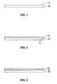
- FIG. 1is a side view of a portion of a support substrate useful in practicing methods in accordance with the present invention
- FIG. 2is a side view of the portion of the support substrate of FIG. 1 , including a layer of sacrificial material applied thereto;
- FIG. 3is a side view of the portion of the support substrate of FIG. 2 , including a layer of etch stop material applied thereto over the layer of sacrificial material;
- FIG. 4is a side cross-sectional view of a support substrate having the structure of FIG. 3 after further processing, depicting a plurality of redistribution layers formed thereon in accordance with the present invention
- FIG. 5is a side cross-sectional view of a wafer level assembly comprising the support substrate of FIG. 4 with semiconductor dice attached to the plurality of redistribution layers;
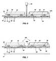
- FIG. 6is a side cross-sectional view of the support substrate of FIG. 5 in the process of scribing of the sacrificial layer in accordance with one aspect of the present invention
- FIG. 7is a side cross-sectional view of separated or singulated semiconductor packages resulting from scribing of the support substrate
- FIG. 8is a side cross-sectional view of the resulting semiconductor packages of FIG. 7 , readied for attachment to a carrier substrate in a flip-chip fashion;
- FIG. 9is a side cross-sectional view of the semiconductor substrate of FIG. 5 , in the process of scribing of the support substrate in accordance with another aspect of the present invention.
- FIG. 10is a side cross-sectional view of a plurality of mutually attached semiconductor packages resulting from scribing of the support substrate;
- FIG. 11is a side cross-sectional view of the mutually attached semiconductor packages of FIG. 10 , readied for attachment to a carrier substrate in a flip-chip fashion;
- FIG. 12is a schematic side view of another embodiment of a wafer level assembly according to the present invention employing a wafer bearing a plurality of unsingulated semiconductor dice and FIG. 12A is a schematic side view of a semiconductor component package fabricated therefrom.
- the present inventioncomprises methods for creating semiconductor packages employing redistribution layers including only selected dice, such as known good die and forming a thinner final semiconductor component assembly than is possible with conventional techniques, as well as the semiconductor component packages and substrates created by the inventive methods.
- the embodiments herein described, while illustrating certain specific and exemplary implementations of the present invention,are not intended to limit the invention or the scope of the appended claims. Those of ordinary skill in the art will also understand that various combinations or modifications of the disclosed, exemplary embodiments and individual features and elements thereof may be made without departing from the scope of the invention.
- Support substrate 10may comprise any material capable of supporting additional layers.
- a substrate comprising siliconas formed in the art by growing a single crystal wafer in the form of a cylinder, which is then segmented or sliced, such as a wafer, may be used.
- another bulk semiconductor substratemay be employed, such as a silicon-on-sapphire (SOS) substrate, or a silicon-on-glass (SOG) substrate, or other type of silicon-on-insulator (SOI) substrate.
- SOSsilicon-on-sapphire
- SOGsilicon-on-glass
- the support substrate 10may be a semiconductor wafer or may be of another material and sized as a conventional semiconductor wafer.
- the support substrate 10may, as desired, have any suitable shape, as long as a substantially planar upper surface 11 is provided.
- the support substrate 10may thus be formed as a planar disk or a planar polygonal substrate, all such structures falling within the scope of the present invention.
- FIG. 2shows the support substrate 10 of FIG. 1 with a sacrificial layer 12 disposed on the planar upper surface 11 thereof.
- Sacrificial layer 12may comprise any suitable material selected for its suitability for etching with a suitable etchant in practicing the methods of the present invention, as will be explained in further detail herein.
- a flowable silicon oxide (SiOx) materialsuch as silicon dioxide, may be deposited by CVD at a temperature of about 125° C. to a thickness of from about 500 ⁇ to about 5000 ⁇ for use as a sacrificial layer 12 , where an acidic etchant, such as an HF solution, is to be used.
- an aluminum sacrificial layermay be used where the etchant is H 2 SO 4 and H 2 O 2 in aqueous solution.
- suitable sacrificial layer materialsinclude, for example, borophosphosilicate glass (BPSG) and TEOS, in association with suitable etch stop materials.
- Sacrificial layer 12may be deposited on the support substrate 10 in any suitable fashion, including chemical vapor deposition (CVD), physical vapor deposition (PVD, also known as sputtering) flowing, spin coating, or in any other manner suitable for the selected material.
- Etch stop layer 14is depicted deposited on sacrificial layer 12 .
- Etch stop layer 14may be any suitable material that has a significantly slower etch rate in comparison to the etch rate exhibited by the sacrificial layer 12 to the selected etchant.
- an etch stop layer 14 of TEOS of about 100 ⁇ in thicknessmay be used as an etch stop with either of the exemplary materials for sacrificial layer 12 and associated etchant combinations discussed in the preceding paragraph.
- other materials including polyimides and other polymeric materialsmay be suitable for use in forming the etch stop layer 14 , and all such materials are within the scope of the present invention.
- the etch stop layer 14may be deposited upon the sacrificial layer using any method suitable for the etch stop material selected, such as flowing, spin coating, CVD, sputtering, or as otherwise known to those of ordinary skill in the art.
- Redistribution layer 15including a plurality of conductive lines or traces 18 for rerouting contact locations of semiconductor dice to be mounted on support substrate 10 , may then be formed on the etch stop layer 14 , as shown in FIG. 4 .
- Redistribution layercomprises a dielectric material 16 , such as BCB, a polyimide, TEOS, silicon nitride, a photosensitive dielectric, phosphosilicate glass (PSG), borosilicate glass (BSG), borophosphosilicate glass (BPSG) or any other suitable dielectric or passivating material containing one or more levels of embedded electrically conductive lines or traces 18 .
- Dielectric material 16may be applied to the surface of etch stop layer 14 by, for example, spin coating, CVD, PECVD or any other suitable method, depending on the selected material.
- the conductive lines or traces 18may comprise a metallic material, such as gold, copper, aluminum or alloys thereof, although it will be appreciated that other conductive materials, such as other metals, or conductive polymeric materials, such as conductive epoxies, may be used.
- the conductive lines or traces 18may be formed as a blanket layer of conductive material deposited on an underlying layer of dielectric material 16 , the blanket layer being masked, photolithographically patterned and etched to define conductive lines or traces 18 prior to deposition of an overlying layer of dielectric material 16 .
- aluminum or coppermay be deposited by physical vapor deposition (sputtering). Copper may be electroplated or electrolessly plated.
- deposited nanoparticlesmay be used for trace formation, using atomic layer deposition (ALD) techniques. It is further contemplated that metallic organic chemical vapor deposition (MOCVD) techniques may be used to deposit, for example, aluminum, tungsten, copper or gold.
- ALDatomic layer deposition
- MOCVDmetallic organic chemical vapor deposition
- a polymer or other dielectric layermay be applied to etch stop layer 14 and trenches in the form of trace patterns etched therein or, if a photosensitive polymer is employed, the trenched trace patterns may be formed therein by appropriate masking and patterning of a photoresist followed by exposure to a selected wavelength or wavelength range of light (for example, UV) to effect a cure of the exposed portions of the photopolymer.
- a UV laser beammay be traversed across the photopolymer in a controlled manner to “write” the recesses wherein traces may be placed by curing the surrounding portions of the photopolymer.
- a blanket layermay be applied and cured to form a dielectric bottom for the trenches to be formed for receipt of conductive material.
- the tracesmay be formed by conventional damascene processing comprising blanket deposition of a conductive material followed by planarization of the structure to remove the conductive material in excess of that in the trenches. Fabrication of redistribution layer 15 may be simplified by using a single material, for example, a polyimide, for both the etch stop layer 14 and dielectric material 16 .
- conductive lines or traces 18are formed, another layer of dielectric material 16 , which may comprise the same or a different material as that of the dielectric material 16 underlying the conductive lines or traces 18 , may be deposited over lines or traces 18 . Subsequent to such deposition, apertures may be etched or otherwise defined (as by patterning of a photopolymer) to expose portions of conductive lines or traces for connection to semiconductor dice to be mounted to support substrate 10 . Notably, additional metallization may be formed in the apertures in contact with the conductive lines or traces in the form of single or multiple layers to form conductive vias, enlarged conductive pads (such as terminal pads 22 ) on the surface of the upper layer of dielectric material, or both, as known in the art.
- redistribution lines or traces 18may comprise one or more levels, as may be required for a specific application, including the final intended use of the semiconductor packages.
- conductive viasmay be formed to connect, and in combination with multiple levels of lines or traces 18 using conventional techniques such as dual damascene processing.
- conductive viasmay be so formed below the lowermost (or a single) level of conductive lines or traces 18 to extend to etch stop layer 14 .
- conductive lines or traces 18may include terminal pads 20 formed in apertures in the underlying portion of the dielectric layer on which the conductive lines or traces 18 are formed, immediately adjacent the etch stop layer 14 for subsequent connection of the resulting semiconductor component packages to external circuitry.
- terminal pads 22may be formed in apertures in an overlying layer of dielectric material 16 above and in combination with conductive lines or traces 18 in contact therewith at the upper level of the redistribution layer 15 for connecting to semiconductor dice 30 ( FIG. 5 ).
- At least one semiconductor die 30may be connected to the conductive lines or traces 18 by placing discrete conductive elements 32 , such as solder balls, other metal or alloy balls, metal coated polymer balls, bumps or studs, or bumps or pillars of conductive or conductor-filled epoxy (or, alternatively, a layer of an anisotropic (Z-axis) conductive adhesive) in mechanical and electrical contact with the terminal pads 22 , as depicted in FIG. 5 , to form a wafer level assembly 100 . As depicted, this may be accomplished by the attachment of the die 30 to the substrate in a flip-chip manner with discrete conductive elements 32 disposed on a like pattern of terminal pads 22 .
- discrete conductive elements 32such as solder balls, other metal or alloy balls, metal coated polymer balls, bumps or studs, or bumps or pillars of conductive or conductor-filled epoxy (or, alternatively, a layer of an anisotropic (Z-axis) conductive adhesive
- solder ballsare employed, a conventional reflow process may be employed to effect the connection, whereas if a conductive or conductor-filled epoxy is employed, a heat-induced cure may be effected by placing the assembly in an oven.
- a so-called “B” stage epoxymay be employed to effect a tacky adhesion of the semiconductor dice 30 to redistribution layer 15 prior to a complete cure of the epoxy.
- each semiconductor die 30 and conductive lines or traces 18may then be encapsulated for protection. Encapsulation may be accomplished by flowing a dielectric underfill material 34 into the space or standoff between each semiconductor die 30 and the redistribution layer on support substrate 10 .
- Suitable underfill materialsmay include epoxies, polymers and other suitable nonconductive materials that may be flowed into and around an array of discrete conductive elements 32 to provide a more robust mechanical connection between each semiconductor die 30 and redistribution layer 15 and protect the connection effected by discrete conductive elements 32 .
- an anisotropic conductive layeris employed, use of an underfill is unnecessary.
- the entire semiconductor die 30may be encapsulated in a molding compound 34 A, rather than merely disposing an underfill material 34 below the dice.
- an underfill material 34may first be disposed between a semiconductor die 30 and redistribution layer 15 prior to encapsulation of the sides and back side of the die.
- Encapsulation of a semiconductor die 30may be effected by any suitable method, such as by screen printing molding compound 34 A over the semiconductor die 30 or by dipping the attached semiconductor dice 30 into a molding compound 34 A.
- Molding compound 34 Amay be formulated to be cured by photo activation (initiation of cross-linking), heat curing, a combination of the two or as otherwise suitable for the selected molding compound 34 A.
- underfill and encapsulant materials for use in moldingexamples include XKE7817 available from Toshiba; other suitable materials are available from Nitto Denko, Shin-Etsu, Sumitomo and Cookson.
- An example of a suitable material for use in screen printing an underfill or encapsulant materialis the Ablestik RP658-5B available from Ablestik Laboratories of Collinso Dominguez, Calif.; other suitable materials are available from Dexter, Hitachi, Toshiba, Nagase, 3M and Sumitomo. It will be appreciated that the underfill and encapsulant materials identified herein are merely exemplary and any suitable materials known to those of ordinary skill in the art may be used.
- FIG. 6the wafer level assembly 100 of FIG. 5 is depicted undergoing a scribing operation of one aspect of the invention.
- a scribe cutis made between the semiconductor dice 30 through the redistribution layer 15 and etch stop layer 14 to expose the sacrificial layer 12 .
- topor “above” are used relative to the wafer level assembly, and not with regard to any specific orientation thereof.
- the scribe cutmay pass partially through the sacrificial layer 12 , but the depth of the scribe may be controlled so as to not contact and damage the support substrate 10 .
- the material of sacrificial layer 12thus becomes exposed through the scribe cut.
- the scribe cutmay be effected around the periphery of each semiconductor die 30 of a wafer level assembly 100 to result in a number of singulated semiconductor component assemblies each including a semiconductor die 30 , or may be around selected semiconductor dice 30 along other selected scribe lines to result in semiconductor component assemblies containing more that one semiconductor die 30 .
- the scribe operationmay be performed with a cutting laser 50 using ablation of a laser beam.
- Laser ablationmay be effected using any suitable equipment, such as the Model 5000-series lasers, offered currently by ElectroScientific Industries (ESI) of Portland, Oreg.
- ESIElectroScientific Industries
- One specific, suitable piece of equipmentis a 355 nm wavelength UV YAG laser, ESI Model 2700, which may be used to form scribes as little as 25 ⁇ m in width.
- One hundred pulses using this laserwill form a 750 ⁇ m deep aperture through silicon.
- Another suitable laseris the Model 200, offered by Xsil Limited of Dublin, Ireland.
- the scribingmay be performed by an abrasive cutting wheel, a diamond bearing dicing saw, or by etching through redistribution layer 15 and etch stop layer 14 with one or more suitable anisotropic etchants after the scribe lines have been defined with a photoresist mask.
- a suitable etchantmay be provided to the sacrificial layer 12 to lift off, or remove, same.
- an acidic etchantsuch as an HF solution at a 20:1 dilution may be used and the sacrificial layer removed in about 10 seconds.
- the sacrificial layer 12is aluminum, H 2 SO 4 and H 2 O 2 in aqueous, deionized (DI) water solution may be employed.
- DIdeionized
- Other etchantsmay be selected based on the composition of the sacrificial layer 12 and etch stop layer 14 .
- Sacrificial layer 12may be etched away by the etchant, which may be provided in a fluid (liquid or gaseous) form.
- a wet etchantdesirably wicks along the sacrificial layer 12 as it etches it.
- a spin etchmay be used.
- the singulated or otherwise segregated semiconductor dice 30 with attached redistribution layers 15may thus be easily removed from the support substrate 10 , resulting in the individual semiconductor component packages 102 , as depicted in FIG. 7 .
- the support substrate 10which remains undamaged by the scribing and etching processes, may then be cleaned and reused. Notably, since the etch stop layer 14 extends over terminal pads 20 , they remain undamaged by the etchant.
- the etch stop layer 14may then be removed from the bottom of the redistribution layer 15 to expose the terminal pads 20 . Removal of the etch stop layer 14 may be performed over the entire lower surface of the resulting package 102 , or only at selected locations, such as those of the terminal pads 20 (or other under bump metallization previously fabricated). Removal may be performed by stripping the etch stop layer 14 with a plasma treatment, etching the etch stop layer 14 with a suitable selected etchant, physical removal as by abrasive techniques, such as chemical mechanical polishing, or as otherwise known to those of ordinary skill in the art.
- Discrete conductive elements 103 in the form of solder balls, other metal or alloy balls, metal coated polymer balls, bumps or studs, or bumps or pillars of conductive or conductor-filled epoxymay be disposed or formed on the terminal pads 20 (or on other suitable under bump metallization previously fabricated) as depicted in FIG. 8 , enabling mounting of the resulting semiconductor component packages 102 on a carrier substrate.
- the resulting semiconductor component packages 102may thus be formed, if desired, using only semiconductor dice 30 that have been qualified as known good dice and the overall thickness of the semiconductor component packages 102 may be reduced in comparison to packages where the redistribution layers are formed directly on a surface of the semiconductor die, as the semiconductor dice 30 employed in the present invention may be thinned by conventional chemical (etching), mechanical (abrasion) or chemical/mechanical (chemically assisted abrasion in the form of chemical/mechanical polishing) techniques to a thickness of less than about 10 ⁇ m prior to application to the redistribution layer 15 , as the required thickness and structural support for handling and further processing is provided by the support substrate 10 , which is then removed.
- etchingchemical (etching), mechanical (abrasion) or chemical/mechanical (chemically assisted abrasion in the form of chemical/mechanical polishing) techniques to a thickness of less than about 10 ⁇ m prior to application to the redistribution layer 15 , as the required thickness and structural support for handling and further processing is provided by the support substrate 10
- Thinning of semiconductor dice 30may be performed by so-called “back grinding” (such term including both mechanical and chemical thinning techniques) at the wafer level before the semiconductor dice 30 are applied to the redistribution layer 15 .
- back grindingsuch term including both mechanical and chemical thinning techniques
- FIGS. 9, 10 and 11a second aspect of the method of the present invention that may be employed for separating the support substrate 10 from the redistribution layer 15 is depicted.
- the wafer level assembly 100 of FIG. 5is depicted undergoing a scribing operation, wherein support substrate 10 is scribed completely therethrough from below to expose the sacrificial layer 12 .
- the term “below”is one of relative orientation with respect to the wafer level assembly 100 and without reference to gravity.
- the wafer level assembly 100may be inverted and scribed.
- the scribe cutmay be of sufficient depth to pass partially through the sacrificial layer 12 but not contact the etch stop layer 14 . Sacrificial layer 12 thus becomes exposed through the scribe cut through the support substrate 10 .
- the scribe operationmay be performed with an abrasive cutting wheel 52 . It will be appreciated that the scribing operation may be conducted by laser ablation, by using a dicing saw, or by masking and etching, as has been described previously herein.
- Sacrificial layer 12may then be etched away by the etchant, which may be provided in a fluid (liquid or gaseous) form. As described previously, a wet etchant may be used so as to wick along the sacrificial layer 12 as it etches.
- the semiconductor dice 30with attached, unsevered redistribution layer 15 , may thus be removed from the support substrate 10 , resulting in a multi-die semiconductor package structure 104 , depicted in FIG. 10 .
- the multi-die semiconductor package structure 104may be treated to remove all or selected portions of the etch stop layer 14 , as discussed previously herein.
- the multi-die semiconductor package structure 104may thus comprise a low profile, multichip module (MCM) with discrete conductive elements 103 attached to the terminal pads 20 thereof for mounting on a carrier substrate, as depicted in FIG. 11 .
- MCMmultichip module
- scribing from below, while sacrificing the support substrate,enables a rapid, economical wafer level attach of discrete conductive elements 103 .
- individual semiconductor component packages 102each including a single semiconductor die 30 , may be singulated, or groups (four, six, eight, etc.) of semiconductor dice interconnected by conductive lines or traces 18 of redistribution layer 15 may be severed to form MCMs.
- grouped semiconductor dice 30be interconnected through redistribution layer 15 , as such interconnection may be effected through circuitry on a carrier substrate to which the grouped semiconductor dice are mounted.
- the present inventionmay also be effected using an unsingulated wafer 200 bearing a plurality of semiconductor dice 30 aligned with and secured to a redistribution layer 15 residing on a support substrate 10 carrying a sacrificial layer 12 and an etch stop layer 14 through discrete conductive elements 32 , as described with respect to the previous embodiments.
- the resulting wafer level assembly 100 ′may then be scribed from above, and singulated semiconductor dice 30 or groups of semiconductor dice 30 with associated redistribution layers 15 are removed from support substrate after etching of sacrificial layer 12 . Underfilling with a dielectric material 34 may be effected, as desired, before or after singulation.
- wafer 200may be thinned as depicted in broken line 202 either prior to or after being secured to support substrate 10 by the mechanical and electrical connections provided by discrete conductive elements 32 .
- the resulting semiconductor component packages 102 ′may then be further processed, as by application of discrete conductive elements 103 and additional packaging material, such as a dielectric coating or encapsulant 34 A, placed over the sides or back sides of the packages 102 ′, or both, as shown. Note that underfilling may be effected concurrently with the back side and side encapsulation, if desired.
- the wafer level assembly 100 ′may be scribed from below, the unsingulated redistribution layer 15 removed from support substrate 10 , all of the dice conductively bumped at the wafer level, and then semiconductor component packages 102 ′ singulated or removed in groups and further processed, as desired or required.
Landscapes
- Engineering & Computer Science (AREA)
- Microelectronics & Electronic Packaging (AREA)
- Computer Hardware Design (AREA)
- Power Engineering (AREA)
- Physics & Mathematics (AREA)
- Condensed Matter Physics & Semiconductors (AREA)
- General Physics & Mathematics (AREA)
- Manufacturing & Machinery (AREA)
- Ceramic Engineering (AREA)
- Dicing (AREA)
- Internal Circuitry In Semiconductor Integrated Circuit Devices (AREA)
Abstract
Description
- 1. Field of the Invention
- The present invention relates generally to the field of integrated circuits including redistribution layer lines or traces and other interconnect structures and, more particularly, although not necessarily limited to, low profile, packaged integrated circuits including a redistribution layer comprising one or more levels of lines, and methods for their fabrication.
- 2. State of the Art
- In order to function, integrated circuits must be in electrical communication with signal inputs and outputs as well as power and ground or bias connections external to the integrated circuit. For example, power and ground or other reference voltage must be supplied for operation of the integrated circuit, and other connections, such as for input, output and timing signals, may also be required. These connections are typically made through leads or other conductive elements connected to bond pads present on the active surface of a semiconductor die incorporating the integrated circuit.
- As electronic devices have become smaller and more sophisticated, the challenge of expanding capabilities while minimizing the space, or “real estate,” also termed the “footprint,” used by an integrated circuit has continued to increase. Techniques for reducing the space used by a semiconductor package include the use of a redistribution layer (RDL) as an additional level of wiring to reposition input and output (I/O) contact locations from the perimeter or center of the active surface to alternative locations. This redistribution process may be necessary if perimeter or central bond pads have to be rerouted into another I/O layout. For example, if the perimeter pad pitch is too fine or does not match the terminal pad layout of a substrate on which the semiconductor die is to be mounted, repositioning may be required. One common example of a redistribution approach is to redistribute a central bond pad layout into a two-dimension array over the active surface of the semiconductor die, the redistributed contact locations then being topped with discrete conductive elements such as solder balls to form a so-called ball grid array.
- In a conventional redistribution structure, redistribution layer lines or traces may be embedded into a dielectric material on a surface of a semiconductor die. Typically, the lines or traces are formed on a dielectric layer, and another dielectric layer is then formed over the lines or traces, the ends of the lines or traces at the redistributed contact locations remaining exposed for subsequent disposition or formation of discrete conductive elements thereon. Suitable dielectric materials may include BCB, polyimide, or photosensitive dielectrics. The process employed depends on whether the redistribution lines or traces are formed of aluminum or copper. For aluminum or copper traces, the metal may be sputtered onto the wafer and the traces etched using a photolithography-defined etch mask. In case of copper traces, the metal may be electroplated and then similarly etched to form traces. A layer of dielectric material may then be deposited over and around the traces and apertures formed therethrough to expose the new contact locations. In another approach, commonly termed a damascene process, the lines or traces may be deposited into recesses formed in a dielectric layer. In yet another approach, preformed lines or traces carried on a dielectric film may be applied to the surface of the semiconductor chip. Redistribution lines or traces are typically employed on the active surface of a semiconductor die to enable so-called “flip-chip” mounting of the semiconductor die with its active surface facing the carrier substrate.
- For ease of processing, RDLs are conventionally formed simultaneously on a large plurality of semiconductor dice at the wafer level, over the entire surface of a semiconductor wafer. The RDL process is thus performed for every potential semiconductor die in a wafer, including those that may have manufacturing defects and are inoperable or fail to meet desired specifications. Significant materials can thus be wasted in processing useless dice. Further, in order to allow the wafer to undergo the processing needed to form the RDLs, the wafer must be of sufficient thickness to be handled by processing equipment without the risk of damage to the physical structure or integrated circuitry of the wafer. This requirement limits the amount of thinning that can be done to the wafer prior to forming the RDLs. Once RDL formation is completed, thinning the wafer is then constrained by the need to protect the wafer surface from etchants used in chemical thinning, the stress to which the wafer may be subjected without damage during mechanical thinning, known as “back grinding,” or debris created by use of a mechanical thinning process.
- Accordingly, a method or system that would be able to effectively form RDLs for semiconductor packages using only semiconductor dice that have been qualified as known good dice (KGD) would be an improvement in the art. Such a technique would enable the fabrication of thin, or low profile, semiconductor packages providing an improvement in the art.
- The present invention includes, in a number of embodiments, methods for creating redistribution layers that may be employed only with selected semiconductor dice (such as dice that have been tested and characterized as known good dice) and that result in a low profile semiconductor component assembly or package.
- In one embodiment of the present invention, a sacrificial layer is deposited on a support substrate. An etch stop layer having a lower etch rate than the sacrificial layer is deposited over the sacrificial layer. Redistribution lines or traces may then be formed on the support substrate atop the etch stop layer. Semiconductor dice configured for flip-chip attachment by disposition of discrete conductive elements on the active surface thereof may then be mechanically and electrically connected to the redistribution lines or traces and the resulting assembly may be underfilled, encased in a dielectric molding compound, or both.
- In one aspect of the method of the present invention, the resulting assembly may then be scribed from the top to expose the sacrificial layer and allow it to be etched to separate or singulate each semiconductor die and its associated redistribution layer from one another and to facilitate removal of the singulated assemblies from the support substrate. Scribing from the top of the assembly and around the semiconductor die peripheries, followed by etching of the sacrificial layer, enables reuse of the support substrate.
- In another aspect of the method of the present invention, the support substrate may be scribed through from below to enable multi-die assemblies mechanically connected by the sacrificial and etch stop layers and, optionally, electrically connected by suitably configured traces of associated redistribution layers, to be removed from the support substrate as multi-die modules. The sacrificial layer may then be removed by etching and the etch stop layer removed to enable mechanical and electrical access to the redistribution lines from the bottom of the assemblies, so that all of the semiconductor dice may have conductive bumps substantially concurrently applied to the redistribution layer at the wafer level, followed by singulation of semiconductor component packages including one or more dice.
- With either of the foregoing approaches, the semiconductor dice employed may be thinned to an extreme degree, since the structure of the semiconductor dice is not load bearing or otherwise stressed. In one approach to thinning, the semiconductor dice may be thinned while still part of their wafer of origin, for example prior to a wafer-level burn-in to qualify selected dice as known good dice. The qualified dice may then be picked from the wafer after singulation, as known in the art, and placed at appropriate locations on the redistribution layer carried by the support substrate. In another approach to thinning, the semiconductor dice are only partially, or not at all, thinned at the wafer level, and when subsequently singulated are placed on the redistribution layer in a form at or close to the original wafer thickness. The array of semiconductor dice secured to the support substrate via the redistribution layer are then thinned in place, resulting in very precise planarity, good surface finish, low thickness variation, and ease or process as well as low cost.
- In a further embodiment of the invention, a wafer of unsingulated, flip-chip configured semiconductor dice may be aligned with and mechanically and electrically connected to a wafer level redistribution layer carried on a support substrate, as previously described. The resulting wafer level assembly may then be scribed from the top, singulating the semiconductor dice or groups of dice at the same time the redistribution layer and underlying etch stop layer are scribed through. Alternatively, when scribing from the bottom of the wafer level assembly, the unsingulated redistribution layer with attached unsingulated wafer bearing the semiconductor dice may be removed, conductive bumps applied, and the assembly subsequently segmented into semiconductor component packages.
- In other embodiments, semiconductor component assemblies and packages fabricated in accordance with the methods of the present invention are also encompassed by the present invention
- In the drawings, which, in conjunction with the accompanying text, disclose the best mode presently known to the inventors for carrying out the present invention:
FIG. 1 is a side view of a portion of a support substrate useful in practicing methods in accordance with the present invention;FIG. 2 is a side view of the portion of the support substrate ofFIG. 1 , including a layer of sacrificial material applied thereto;FIG. 3 is a side view of the portion of the support substrate ofFIG. 2 , including a layer of etch stop material applied thereto over the layer of sacrificial material;FIG. 4 is a side cross-sectional view of a support substrate having the structure ofFIG. 3 after further processing, depicting a plurality of redistribution layers formed thereon in accordance with the present invention;FIG. 5 is a side cross-sectional view of a wafer level assembly comprising the support substrate ofFIG. 4 with semiconductor dice attached to the plurality of redistribution layers;FIG. 6 is a side cross-sectional view of the support substrate ofFIG. 5 in the process of scribing of the sacrificial layer in accordance with one aspect of the present invention;FIG. 7 is a side cross-sectional view of separated or singulated semiconductor packages resulting from scribing of the support substrate;FIG. 8 is a side cross-sectional view of the resulting semiconductor packages ofFIG. 7 , readied for attachment to a carrier substrate in a flip-chip fashion;FIG. 9 is a side cross-sectional view of the semiconductor substrate ofFIG. 5 , in the process of scribing of the support substrate in accordance with another aspect of the present invention;FIG. 10 is a side cross-sectional view of a plurality of mutually attached semiconductor packages resulting from scribing of the support substrate;FIG. 11 is a side cross-sectional view of the mutually attached semiconductor packages ofFIG. 10 , readied for attachment to a carrier substrate in a flip-chip fashion; andFIG. 12 is a schematic side view of another embodiment of a wafer level assembly according to the present invention employing a wafer bearing a plurality of unsingulated semiconductor dice andFIG. 12A is a schematic side view of a semiconductor component package fabricated therefrom.- The present invention comprises methods for creating semiconductor packages employing redistribution layers including only selected dice, such as known good die and forming a thinner final semiconductor component assembly than is possible with conventional techniques, as well as the semiconductor component packages and substrates created by the inventive methods. The embodiments herein described, while illustrating certain specific and exemplary implementations of the present invention, are not intended to limit the invention or the scope of the appended claims. Those of ordinary skill in the art will also understand that various combinations or modifications of the disclosed, exemplary embodiments and individual features and elements thereof may be made without departing from the scope of the invention.
- Turning to
FIG. 1 , there is depicted asupport substrate 10.Support substrate 10 may comprise any material capable of supporting additional layers. For example, a substrate comprising silicon, as formed in the art by growing a single crystal wafer in the form of a cylinder, which is then segmented or sliced, such as a wafer, may be used. Alternatively, another bulk semiconductor substrate may be employed, such as a silicon-on-sapphire (SOS) substrate, or a silicon-on-glass (SOG) substrate, or other type of silicon-on-insulator (SOI) substrate. Other substrates that are suitable for supporting additional layers and semiconductor dice thereon, such as BT resin, FR-4 and FR-5 laminates, ceramic substrates, metallic plates or polymeric materials formed into a substrate having a substantially planar upper surface may be used. In order to enable handling and processing with conventional equipment, thesupport substrate 10 may be a semiconductor wafer or may be of another material and sized as a conventional semiconductor wafer. However, thesupport substrate 10 may, as desired, have any suitable shape, as long as a substantially planarupper surface 11 is provided. Thesupport substrate 10 may thus be formed as a planar disk or a planar polygonal substrate, all such structures falling within the scope of the present invention. FIG. 2 shows thesupport substrate 10 ofFIG. 1 with asacrificial layer 12 disposed on the planarupper surface 11 thereof.Sacrificial layer 12 may comprise any suitable material selected for its suitability for etching with a suitable etchant in practicing the methods of the present invention, as will be explained in further detail herein. For example, a flowable silicon oxide (SiOx) material, such as silicon dioxide, may be deposited by CVD at a temperature of about 125° C. to a thickness of from about 500 Å to about 5000 Å for use as asacrificial layer 12, where an acidic etchant, such as an HF solution, is to be used. Similarly, an aluminum sacrificial layer may be used where the etchant is H2SO4and H2O2in aqueous solution. Other suitable sacrificial layer materials include, for example, borophosphosilicate glass (BPSG) and TEOS, in association with suitable etch stop materials.Sacrificial layer 12 may be deposited on thesupport substrate 10 in any suitable fashion, including chemical vapor deposition (CVD), physical vapor deposition (PVD, also known as sputtering) flowing, spin coating, or in any other manner suitable for the selected material.- Turning to
FIG. 3 , anetch stop layer 14 is depicted deposited onsacrificial layer 12.Etch stop layer 14 may be any suitable material that has a significantly slower etch rate in comparison to the etch rate exhibited by thesacrificial layer 12 to the selected etchant. For example, anetch stop layer 14 of TEOS of about 100 Å in thickness may be used as an etch stop with either of the exemplary materials forsacrificial layer 12 and associated etchant combinations discussed in the preceding paragraph. Of course, other materials including polyimides and other polymeric materials may be suitable for use in forming theetch stop layer 14, and all such materials are within the scope of the present invention. Similarly, theetch stop layer 14 may be deposited upon the sacrificial layer using any method suitable for the etch stop material selected, such as flowing, spin coating, CVD, sputtering, or as otherwise known to those of ordinary skill in the art. Redistribution layer 15, including a plurality of conductive lines or traces18 for rerouting contact locations of semiconductor dice to be mounted onsupport substrate 10, may then be formed on theetch stop layer 14, as shown inFIG. 4 . Redistribution layer comprises adielectric material 16, such as BCB, a polyimide, TEOS, silicon nitride, a photosensitive dielectric, phosphosilicate glass (PSG), borosilicate glass (BSG), borophosphosilicate glass (BPSG) or any other suitable dielectric or passivating material containing one or more levels of embedded electrically conductive lines or traces18.Dielectric material 16 may be applied to the surface ofetch stop layer 14 by, for example, spin coating, CVD, PECVD or any other suitable method, depending on the selected material.- The conductive lines or traces18 may comprise a metallic material, such as gold, copper, aluminum or alloys thereof, although it will be appreciated that other conductive materials, such as other metals, or conductive polymeric materials, such as conductive epoxies, may be used. The conductive lines or traces18 may be formed as a blanket layer of conductive material deposited on an underlying layer of
dielectric material 16, the blanket layer being masked, photolithographically patterned and etched to define conductive lines or traces18 prior to deposition of an overlying layer ofdielectric material 16. For example, aluminum or copper may be deposited by physical vapor deposition (sputtering). Copper may be electroplated or electrolessly plated. It is also contemplated that deposited nanoparticles may be used for trace formation, using atomic layer deposition (ALD) techniques. It is further contemplated that metallic organic chemical vapor deposition (MOCVD) techniques may be used to deposit, for example, aluminum, tungsten, copper or gold. - In another approach and as desired, a polymer or other dielectric layer may be applied to etch
stop layer 14 and trenches in the form of trace patterns etched therein or, if a photosensitive polymer is employed, the trenched trace patterns may be formed therein by appropriate masking and patterning of a photoresist followed by exposure to a selected wavelength or wavelength range of light (for example, UV) to effect a cure of the exposed portions of the photopolymer. Alternatively, a UV laser beam may be traversed across the photopolymer in a controlled manner to “write” the recesses wherein traces may be placed by curing the surrounding portions of the photopolymer. If a photopolymer is employed, a blanket layer may be applied and cured to form a dielectric bottom for the trenches to be formed for receipt of conductive material. After the trenches are formed, the traces may be formed by conventional damascene processing comprising blanket deposition of a conductive material followed by planarization of the structure to remove the conductive material in excess of that in the trenches. Fabrication ofredistribution layer 15 may be simplified by using a single material, for example, a polyimide, for both theetch stop layer 14 anddielectric material 16. - After conductive lines or traces18 are formed, another layer of
dielectric material 16, which may comprise the same or a different material as that of thedielectric material 16 underlying the conductive lines or traces18, may be deposited over lines or traces18. Subsequent to such deposition, apertures may be etched or otherwise defined (as by patterning of a photopolymer) to expose portions of conductive lines or traces for connection to semiconductor dice to be mounted to supportsubstrate 10. Notably, additional metallization may be formed in the apertures in contact with the conductive lines or traces in the form of single or multiple layers to form conductive vias, enlarged conductive pads (such as terminal pads22) on the surface of the upper layer of dielectric material, or both, as known in the art. - While shown as a single level of laterally extending conductive lines or traces18, redistribution lines or traces18 may comprise one or more levels, as may be required for a specific application, including the final intended use of the semiconductor packages. For example, as known in the art, conductive vias may be formed to connect, and in combination with multiple levels of lines or traces18 using conventional techniques such as dual damascene processing. Similarly, conductive vias may be so formed below the lowermost (or a single) level of conductive lines or traces18 to extend to etch
stop layer 14. Thus, conductive lines or traces18 may includeterminal pads 20 formed in apertures in the underlying portion of the dielectric layer on which the conductive lines or traces18 are formed, immediately adjacent theetch stop layer 14 for subsequent connection of the resulting semiconductor component packages to external circuitry. Similarly and as noted above,terminal pads 22 may be formed in apertures in an overlying layer ofdielectric material 16 above and in combination with conductive lines or traces18 in contact therewith at the upper level of theredistribution layer 15 for connecting to semiconductor dice30 (FIG. 5 ). - At least one semiconductor die30 may be connected to the conductive lines or traces18 by placing discrete
conductive elements 32, such as solder balls, other metal or alloy balls, metal coated polymer balls, bumps or studs, or bumps or pillars of conductive or conductor-filled epoxy (or, alternatively, a layer of an anisotropic (Z-axis) conductive adhesive) in mechanical and electrical contact with theterminal pads 22, as depicted inFIG. 5 , to form awafer level assembly 100. As depicted, this may be accomplished by the attachment of the die30 to the substrate in a flip-chip manner with discreteconductive elements 32 disposed on a like pattern ofterminal pads 22. If solder balls are employed, a conventional reflow process may be employed to effect the connection, whereas if a conductive or conductor-filled epoxy is employed, a heat-induced cure may be effected by placing the assembly in an oven. A so-called “B” stage epoxy may be employed to effect a tacky adhesion of thesemiconductor dice 30 toredistribution layer 15 prior to a complete cure of the epoxy. - The mechanical and electrical connection between each semiconductor die30 and conductive lines or traces18 may then be encapsulated for protection. Encapsulation may be accomplished by flowing a
dielectric underfill material 34 into the space or standoff between each semiconductor die30 and the redistribution layer onsupport substrate 10. Suitable underfill materials may include epoxies, polymers and other suitable nonconductive materials that may be flowed into and around an array of discreteconductive elements 32 to provide a more robust mechanical connection between each semiconductor die30 andredistribution layer 15 and protect the connection effected by discreteconductive elements 32. Of course, if an anisotropic conductive layer is employed, use of an underfill is unnecessary. - In some embodiments, the entire semiconductor die30 may be encapsulated in a
molding compound 34A, rather than merely disposing anunderfill material 34 below the dice. Of course, anunderfill material 34 may first be disposed between asemiconductor die 30 andredistribution layer 15 prior to encapsulation of the sides and back side of the die. Encapsulation of asemiconductor die 30 may be effected by any suitable method, such as by screenprinting molding compound 34A over the semiconductor die30 or by dipping the attachedsemiconductor dice 30 into amolding compound 34A.Molding compound 34A may be formulated to be cured by photo activation (initiation of cross-linking), heat curing, a combination of the two or as otherwise suitable for the selectedmolding compound 34A. Examples of suitable underfill and encapsulant materials for use in molding include XKE7817 available from Toshiba; other suitable materials are available from Nitto Denko, Shin-Etsu, Sumitomo and Cookson. An example of a suitable material for use in screen printing an underfill or encapsulant material is the Ablestik RP658-5B available from Ablestik Laboratories of Rancho Dominguez, Calif.; other suitable materials are available from Dexter, Hitachi, Toshiba, Nagase, 3M and Sumitomo. It will be appreciated that the underfill and encapsulant materials identified herein are merely exemplary and any suitable materials known to those of ordinary skill in the art may be used. - Turning to
FIG. 6 , thewafer level assembly 100 ofFIG. 5 is depicted undergoing a scribing operation of one aspect of the invention. From the top, or above thewafer level assembly 100, a scribe cut is made between thesemiconductor dice 30 through theredistribution layer 15 andetch stop layer 14 to expose thesacrificial layer 12. As used herein, the terms “top” or “above” are used relative to the wafer level assembly, and not with regard to any specific orientation thereof. The scribe cut may pass partially through thesacrificial layer 12, but the depth of the scribe may be controlled so as to not contact and damage thesupport substrate 10. The material ofsacrificial layer 12 thus becomes exposed through the scribe cut. The scribe cut may be effected around the periphery of each semiconductor die30 of awafer level assembly 100 to result in a number of singulated semiconductor component assemblies each including asemiconductor die 30, or may be around selectedsemiconductor dice 30 along other selected scribe lines to result in semiconductor component assemblies containing more that one semiconductor die30. - As depicted in
FIG. 6 , the scribe operation may be performed with a cuttinglaser 50 using ablation of a laser beam. Laser ablation may be effected using any suitable equipment, such as the Model 5000-series lasers, offered currently by ElectroScientific Industries (ESI) of Portland, Oreg. One specific, suitable piece of equipment is a 355 nm wavelength UV YAG laser, ESI Model 2700, which may be used to form scribes as little as 25 μm in width. One hundred pulses using this laser will form a 750 μm deep aperture through silicon. Another suitable laser is theModel 200, offered by Xsil Limited of Dublin, Ireland. Alternatively, the scribing may be performed by an abrasive cutting wheel, a diamond bearing dicing saw, or by etching throughredistribution layer 15 andetch stop layer 14 with one or more suitable anisotropic etchants after the scribe lines have been defined with a photoresist mask. - Once the
sacrificial layer 12 is exposed by the scribe lines, a suitable etchant may be provided to thesacrificial layer 12 to lift off, or remove, same. For example, where the sacrificial layer is a silicon dioxide material, an acidic etchant, such as an HF solution at a 20:1 dilution may be used and the sacrificial layer removed in about 10 seconds. Similarly, where thesacrificial layer 12 is aluminum, H2SO4and H2O2in aqueous, deionized (DI) water solution may be employed. Other etchants may be selected based on the composition of thesacrificial layer 12 andetch stop layer 14. Sacrificial layer 12 may be etched away by the etchant, which may be provided in a fluid (liquid or gaseous) form. A wet etchant desirably wicks along thesacrificial layer 12 as it etches it. In order to prevent damage to exposed sides of integrated circuitry of semiconductor dice by etchant running down the sides thereof, a spin etch may be used. The singulated or otherwise segregatedsemiconductor dice 30 with attached redistribution layers15 may thus be easily removed from thesupport substrate 10, resulting in the individual semiconductor component packages102, as depicted inFIG. 7 . Thesupport substrate 10, which remains undamaged by the scribing and etching processes, may then be cleaned and reused. Notably, since theetch stop layer 14 extends overterminal pads 20, they remain undamaged by the etchant.- The
etch stop layer 14 may then be removed from the bottom of theredistribution layer 15 to expose theterminal pads 20. Removal of theetch stop layer 14 may be performed over the entire lower surface of the resultingpackage 102, or only at selected locations, such as those of the terminal pads20 (or other under bump metallization previously fabricated). Removal may be performed by stripping theetch stop layer 14 with a plasma treatment, etching theetch stop layer 14 with a suitable selected etchant, physical removal as by abrasive techniques, such as chemical mechanical polishing, or as otherwise known to those of ordinary skill in the art. Discreteconductive elements 103 in the form of solder balls, other metal or alloy balls, metal coated polymer balls, bumps or studs, or bumps or pillars of conductive or conductor-filled epoxy may be disposed or formed on the terminal pads20 (or on other suitable under bump metallization previously fabricated) as depicted inFIG. 8 , enabling mounting of the resulting semiconductor component packages102 on a carrier substrate. The resulting semiconductor component packages102 may thus be formed, if desired, usingonly semiconductor dice 30 that have been qualified as known good dice and the overall thickness of the semiconductor component packages102 may be reduced in comparison to packages where the redistribution layers are formed directly on a surface of the semiconductor die, as thesemiconductor dice 30 employed in the present invention may be thinned by conventional chemical (etching), mechanical (abrasion) or chemical/mechanical (chemically assisted abrasion in the form of chemical/mechanical polishing) techniques to a thickness of less than about 10 μm prior to application to theredistribution layer 15, as the required thickness and structural support for handling and further processing is provided by thesupport substrate 10, which is then removed. Thinning ofsemiconductor dice 30 may be performed by so-called “back grinding” (such term including both mechanical and chemical thinning techniques) at the wafer level before thesemiconductor dice 30 are applied to theredistribution layer 15. However, it may also be desirable tosingulate semiconductor dice 30 from their wafer of original without any, or only partial, prior reduction in thickness to provide a more robust structure for testing, handling and a pick-and-place operation to place the semiconductor dice onredistribution layer 15 carried bysupport substrate 10. If the latter approach is taken, then all of the flip-chip attached semiconductor dice secured to supportsubstrate 10 may then be thinned while supported thereon. - Turning to
FIGS. 9, 10 and11, a second aspect of the method of the present invention that may be employed for separating thesupport substrate 10 from theredistribution layer 15 is depicted. As depicted inFIG. 9 , thewafer level assembly 100 ofFIG. 5 is depicted undergoing a scribing operation, whereinsupport substrate 10 is scribed completely therethrough from below to expose thesacrificial layer 12. As used herein, the term “below” is one of relative orientation with respect to thewafer level assembly 100 and without reference to gravity. Thus, thewafer level assembly 100 may be inverted and scribed. The scribe cut may be of sufficient depth to pass partially through thesacrificial layer 12 but not contact theetch stop layer 14.Sacrificial layer 12 thus becomes exposed through the scribe cut through thesupport substrate 10. - As depicted in
FIG. 9 , the scribe operation may be performed with anabrasive cutting wheel 52. It will be appreciated that the scribing operation may be conducted by laser ablation, by using a dicing saw, or by masking and etching, as has been described previously herein. Sacrificial layer 12 may then be etched away by the etchant, which may be provided in a fluid (liquid or gaseous) form. As described previously, a wet etchant may be used so as to wick along thesacrificial layer 12 as it etches. Thesemiconductor dice 30, with attached,unsevered redistribution layer 15, may thus be removed from thesupport substrate 10, resulting in a multi-die semiconductor package structure104, depicted inFIG. 10 . The multi-die semiconductor package structure104 may be treated to remove all or selected portions of theetch stop layer 14, as discussed previously herein. The multi-die semiconductor package structure104 may thus comprise a low profile, multichip module (MCM) with discreteconductive elements 103 attached to theterminal pads 20 thereof for mounting on a carrier substrate, as depicted inFIG. 11 . Notably, scribing from below, while sacrificing the support substrate, enables a rapid, economical wafer level attach of discreteconductive elements 103. Following the wafer level attach of discreteconductive elements 103, individual semiconductor component packages102, each including a single semiconductor die30, may be singulated, or groups (four, six, eight, etc.) of semiconductor dice interconnected by conductive lines or traces18 ofredistribution layer 15 may be severed to form MCMs. Of course, it is not required that groupedsemiconductor dice 30 be interconnected throughredistribution layer 15, as such interconnection may be effected through circuitry on a carrier substrate to which the grouped semiconductor dice are mounted.- As schematically depicted in
FIG. 12 , the present invention may also be effected using anunsingulated wafer 200 bearing a plurality ofsemiconductor dice 30 aligned with and secured to aredistribution layer 15 residing on asupport substrate 10 carrying asacrificial layer 12 and anetch stop layer 14 through discreteconductive elements 32, as described with respect to the previous embodiments. The resultingwafer level assembly 100′ may then be scribed from above, andsingulated semiconductor dice 30 or groups ofsemiconductor dice 30 with associated redistribution layers15 are removed from support substrate after etching ofsacrificial layer 12. Underfilling with adielectric material 34 may be effected, as desired, before or after singulation. As with the previous embodiments of the invention,wafer 200 may be thinned as depicted inbroken line 202 either prior to or after being secured to supportsubstrate 10 by the mechanical and electrical connections provided by discreteconductive elements 32. - The resulting semiconductor component packages102′ (see
FIG. 12A ) may then be further processed, as by application of discreteconductive elements 103 and additional packaging material, such as a dielectric coating orencapsulant 34A, placed over the sides or back sides of thepackages 102′, or both, as shown. Note that underfilling may be effected concurrently with the back side and side encapsulation, if desired. In another approach, thewafer level assembly 100′ may be scribed from below, theunsingulated redistribution layer 15 removed fromsupport substrate 10, all of the dice conductively bumped at the wafer level, and then semiconductor component packages102′ singulated or removed in groups and further processed, as desired or required. - It will be apparent that details of the processes, methods and structures herein described can be varied considerably without departing from the concept and scope of the invention. The claims alone define the scope of the invention as conceived and as described herein.
Claims (64)
Priority Applications (2)
| Application Number | Priority Date | Filing Date | Title |
|---|---|---|---|
| US10/931,678US7268012B2 (en) | 2004-08-31 | 2004-08-31 | Methods for fabrication of thin semiconductor assemblies including redistribution layers and packages and assemblies formed thereby |
| US11/516,243US7589426B2 (en) | 2004-08-31 | 2006-09-06 | Semiconductor assemblies including redistribution layers and packages and assemblies formed therefrom |
Applications Claiming Priority (1)
| Application Number | Priority Date | Filing Date | Title |
|---|---|---|---|
| US10/931,678US7268012B2 (en) | 2004-08-31 | 2004-08-31 | Methods for fabrication of thin semiconductor assemblies including redistribution layers and packages and assemblies formed thereby |
Related Child Applications (1)
| Application Number | Title | Priority Date | Filing Date |
|---|---|---|---|
| US11/516,243DivisionUS7589426B2 (en) | 2004-08-31 | 2006-09-06 | Semiconductor assemblies including redistribution layers and packages and assemblies formed therefrom |
Publications (2)
| Publication Number | Publication Date |
|---|---|
| US20060046350A1true US20060046350A1 (en) | 2006-03-02 |
| US7268012B2 US7268012B2 (en) | 2007-09-11 |
Family
ID=35943804
Family Applications (2)
| Application Number | Title | Priority Date | Filing Date |
|---|---|---|---|
| US10/931,678Expired - LifetimeUS7268012B2 (en) | 2004-08-31 | 2004-08-31 | Methods for fabrication of thin semiconductor assemblies including redistribution layers and packages and assemblies formed thereby |
| US11/516,243Active2025-11-01US7589426B2 (en) | 2004-08-31 | 2006-09-06 | Semiconductor assemblies including redistribution layers and packages and assemblies formed therefrom |
Family Applications After (1)
| Application Number | Title | Priority Date | Filing Date |
|---|---|---|---|
| US11/516,243Active2025-11-01US7589426B2 (en) | 2004-08-31 | 2006-09-06 | Semiconductor assemblies including redistribution layers and packages and assemblies formed therefrom |
Country Status (1)
| Country | Link |
|---|---|
| US (2) | US7268012B2 (en) |
Cited By (42)
| Publication number | Priority date | Publication date | Assignee | Title |
|---|---|---|---|---|
| US20060113639A1 (en)* | 2002-10-15 | 2006-06-01 | Sehat Sutardja | Integrated circuit including silicon wafer with annealed glass paste |
| US20060267194A1 (en)* | 2002-10-15 | 2006-11-30 | Sehat Sutardja | Integrated circuit package with air gap |
| US20060267179A1 (en)* | 2005-05-25 | 2006-11-30 | Harald Gross | Redistribution layer with microstrips |
| US20070176690A1 (en)* | 2002-10-15 | 2007-08-02 | Sehat Sutardja | Crystal oscillator emulator |
| US20070176705A1 (en)* | 2002-10-15 | 2007-08-02 | Sehat Sutardja | Crystal oscillator emulator |
| US20070188254A1 (en)* | 2002-10-15 | 2007-08-16 | Sehat Sutardja | Crystal oscillator emulator |
| US20070210461A1 (en)* | 2006-03-10 | 2007-09-13 | Fay Owen R | Semiconductor device packaging |
| US20070259508A1 (en)* | 2006-05-03 | 2007-11-08 | Ming-Yen Chiu | Method of fabricating microconnectors |
| US20080029297A1 (en)* | 2006-08-01 | 2008-02-07 | Shinko Electric Industries Co., Ltd. | Wiring substrate and manufacturing method thereof, and semiconductor device |
| US20080217773A1 (en)* | 2007-03-09 | 2008-09-11 | Charles Stark Draper Laboratory, Inc. | Removal of integrated circuits from packages |
| US20080258284A1 (en)* | 2007-04-23 | 2008-10-23 | John Trezza | Ultra-thin chip packaging |
| US20090039510A1 (en)* | 2007-08-08 | 2009-02-12 | Casio Computer Co., Ltd. | Semiconductor device and manufacturing method thereof |
| US20090039514A1 (en)* | 2007-08-08 | 2009-02-12 | Casio Computer Co., Ltd. | Semiconductor device and method for manufacturing the same |
| US20090140396A1 (en)* | 2007-11-30 | 2009-06-04 | Ralf Richter | Stressed interlayer dielectric with reduced probability for void generation in a semiconductor device by using an intermediate etch control layer of increased thickness |
| CN100536259C (en)* | 2006-05-15 | 2009-09-02 | 探微科技股份有限公司 | Method for manufacturing micro connector |
| US20090251879A1 (en)* | 2008-04-04 | 2009-10-08 | Thompson Jeffrey C | Die thinning processes and structures |
| US20090250249A1 (en)* | 2008-04-04 | 2009-10-08 | Racz Livia M | Interposers, electronic modules, and methods for forming the same |
| US20090250823A1 (en)* | 2008-04-04 | 2009-10-08 | Racz Livia M | Electronic Modules and Methods for Forming the Same |
| US20100077609A1 (en)* | 2008-09-29 | 2010-04-01 | Xerox Corporation | Buried traces for sealed electrostatic membrane actuators or sensors |
| EP2378550A1 (en)* | 2010-04-14 | 2011-10-19 | Nxp B.V. | Leadless IC package and manufacturing method thereof |
| US20120094439A1 (en)* | 2009-06-12 | 2012-04-19 | 3D Plus | Method for Positioning Chips During the Production of a Reconstituted Wafer |
| WO2012054169A1 (en)* | 2010-10-22 | 2012-04-26 | Harris Corporation | Method of making a multi-chip module having a reduced thickness and related devices |
| US20120175767A1 (en)* | 2011-01-06 | 2012-07-12 | Advanced Semiconductor Engineering, Inc. | Semiconductor package with through silicon vias and method for making the same |
| US20130164889A1 (en)* | 2011-02-14 | 2013-06-27 | Fujitsu Semiconductor Limited | Semiconductor device and method of manufacturing the same |
| US8952528B2 (en)* | 2012-11-20 | 2015-02-10 | Siliconware Precision Industries Co., Ltd. | Semiconductor package and fabrication method thereof |
| US20160071816A1 (en)* | 2014-09-05 | 2016-03-10 | Taiwan Semiconductor Manufacturing Company, Ltd. | Integrated Circuit Packages and Methods of Forming Same |
| US20160155680A1 (en)* | 2014-12-01 | 2016-06-02 | Infineon Technologies Ag | Semiconductor Package and Method of Fabrication Thereof |
| US20160190039A1 (en)* | 2014-12-31 | 2016-06-30 | Siliconware Precision Industries Co., Ltd. | Substrate structure |
| US20170278777A1 (en)* | 2011-11-16 | 2017-09-28 | Taiwan Semiconductor Manufacturing Company, Ltd. | Package Structures and Methods for Forming the Same |
| US20170372985A1 (en)* | 2016-06-24 | 2017-12-28 | Infineon Technologies Ag | LDMOS Transistor and Method |
| US20170372986A1 (en) | 2016-06-24 | 2017-12-28 | Infineon Technologies Ag | LDMOS Transistor and Method |
| US9875933B2 (en) | 2016-06-24 | 2018-01-23 | Infineon Technologies Ag | Substrate and method including forming a via comprising a conductive liner layer and conductive plug having different microstructures |
| CN107799483A (en)* | 2016-08-31 | 2018-03-13 | 日月光半导体制造股份有限公司 | Semiconductor package structure and manufacturing method thereof |
| US9960229B2 (en) | 2016-06-24 | 2018-05-01 | Infineon Technologies Ag | Semiconductor device including a LDMOS transistor |
| US10050139B2 (en) | 2016-06-24 | 2018-08-14 | Infineon Technologies Ag | Semiconductor device including a LDMOS transistor and method |
| US20200144314A1 (en)* | 2018-11-05 | 2020-05-07 | Varex Imaging Corporation | Detector architecture using photodetector substrates and semiconductor devices |
| US20200211883A1 (en)* | 2018-12-28 | 2020-07-02 | Applied Materials, Inc. | Adhesive-less substrate bonding to carrier plate |
| CN112262460A (en)* | 2018-04-10 | 2021-01-22 | 维斯普瑞公司 | Method and apparatus for solderless integration of multiple semiconductor die on flexible substrate |
| US20210217736A1 (en)* | 2016-10-13 | 2021-07-15 | Taiwan Semiconductor Manufacturing Company Ltd. | Semiconductor device and manufacturing method of the same |
| US11094646B2 (en)* | 2006-05-16 | 2021-08-17 | Taiwan Semiconductor Manufacturing Company, Ltd. | Methods of manufacturing an integrated circuit having stress tuning layer |
| CN113871312A (en)* | 2020-06-30 | 2021-12-31 | 美光科技公司 | Semiconductor device assembly with sacrificial post and method of fabricating sacrificial post |
| WO2025077404A1 (en)* | 2023-10-12 | 2025-04-17 | 天芯互联科技有限公司 | Packaging method and packaging body |
Families Citing this family (43)
| Publication number | Priority date | Publication date | Assignee | Title |
|---|---|---|---|---|
| ES2651349T3 (en) | 2005-06-08 | 2018-01-25 | Rigel Pharmaceuticals, Inc. | Compositions and methods for inhibiting the JAK route |
| WO2007000695A2 (en)* | 2005-06-29 | 2007-01-04 | Koninklijke Philips Electronics N.V. | Package, subassembly and methods of manufacturing thereof |
| TWI275187B (en)* | 2005-11-30 | 2007-03-01 | Advanced Semiconductor Eng | Flip chip package and manufacturing method of the same |
| US7682972B2 (en)* | 2006-06-01 | 2010-03-23 | Amitec-Advanced Multilayer Interconnect Technoloiges Ltd. | Advanced multilayer coreless support structures and method for their fabrication |
| US8030138B1 (en)* | 2006-07-10 | 2011-10-04 | National Semiconductor Corporation | Methods and systems of packaging integrated circuits |
| KR100887475B1 (en)* | 2007-02-26 | 2009-03-10 | 주식회사 네패스 | Semiconductor package and manufacturing method |
| US7834449B2 (en)* | 2007-04-30 | 2010-11-16 | Broadcom Corporation | Highly reliable low cost structure for wafer-level ball grid array packaging |
| US7968986B2 (en)* | 2007-05-07 | 2011-06-28 | Innovative Micro Technology | Lid structure for microdevice and method of manufacture |
| US7763980B2 (en)* | 2007-06-28 | 2010-07-27 | Sandisk Corporation | Semiconductor die having a distribution layer |
| US7772047B2 (en)* | 2007-06-28 | 2010-08-10 | Sandisk Corporation | Method of fabricating a semiconductor die having a redistribution layer |
| US7872347B2 (en)* | 2007-08-09 | 2011-01-18 | Broadcom Corporation | Larger than die size wafer-level redistribution packaging process |
| US10074553B2 (en)* | 2007-12-03 | 2018-09-11 | STATS ChipPAC Pte. Ltd. | Wafer level package integration and method |
| US9460951B2 (en) | 2007-12-03 | 2016-10-04 | STATS ChipPAC Pte. Ltd. | Semiconductor device and method of wafer level package integration |
| US7749809B2 (en)* | 2007-12-17 | 2010-07-06 | National Semiconductor Corporation | Methods and systems for packaging integrated circuits |
| US8048781B2 (en)* | 2008-01-24 | 2011-11-01 | National Semiconductor Corporation | Methods and systems for packaging integrated circuits |
| US7791209B2 (en)* | 2008-03-12 | 2010-09-07 | International Business Machines Corporation | Method of underfill air vent for flipchip BGA |
| US7932180B2 (en)* | 2008-07-07 | 2011-04-26 | Infineon Technologies Ag | Manufacturing a semiconductor device via etching a semiconductor chip to a first layer |
| US7923350B2 (en)* | 2008-09-09 | 2011-04-12 | Infineon Technologies Ag | Method of manufacturing a semiconductor device including etching to etch stop regions |
| US8174131B2 (en)* | 2009-05-27 | 2012-05-08 | Globalfoundries Inc. | Semiconductor device having a filled trench structure and methods for fabricating the same |
| CN101924083B (en)* | 2009-06-09 | 2012-07-04 | 日月光半导体制造股份有限公司 | Semiconductor package and manufacturing method thereof |
| US8643164B2 (en)* | 2009-06-11 | 2014-02-04 | Broadcom Corporation | Package-on-package technology for fan-out wafer-level packaging |
| DE102010010937A1 (en)* | 2009-10-26 | 2011-04-28 | MAX-PLANCK-Gesellschaft zur Förderung der Wissenschaften e.V. | Method and device for producing a Fresnel zone plate |
| DE102009060480A1 (en)* | 2009-12-18 | 2011-06-22 | Schweizer Electronic AG, 78713 | Conductor structure element and method for producing a conductor structure element |
| US20110175218A1 (en)* | 2010-01-18 | 2011-07-21 | Shiann-Ming Liou | Package assembly having a semiconductor substrate |
| US20110186960A1 (en)* | 2010-02-03 | 2011-08-04 | Albert Wu | Techniques and configurations for recessed semiconductor substrates |
| DE102011018295B4 (en)* | 2011-04-20 | 2021-06-24 | Austriamicrosystems Ag | Method for cutting a carrier for electrical components |
| US9859028B2 (en) | 2012-03-08 | 2018-01-02 | Max-Planck-Gesellschaft Zur Foerderung Der Wissenschaften E.V. | Method of producing a Fresnel Zone Plate for applications in high energy radiation |
| US9023690B2 (en)* | 2012-11-19 | 2015-05-05 | United Test And Assembly Center | Leadframe area array packaging technology |
| US10128175B2 (en)* | 2013-01-29 | 2018-11-13 | Taiwan Semiconductor Manufacturing Company | Packaging methods and packaged semiconductor devices |
| KR20140101984A (en)* | 2013-02-13 | 2014-08-21 | 삼성전자주식회사 | Semiconductor pacakge and method of forming the package |
| US9049791B2 (en)* | 2013-06-07 | 2015-06-02 | Zhuhai Advanced Chip Carriers & Electronic Substrates Solutions Technologies Co. Ltd. | Terminations and couplings between chips and substrates |
| US10418298B2 (en) | 2013-09-24 | 2019-09-17 | STATS ChipPAC Pte. Ltd. | Semiconductor device and method of forming dual fan-out semiconductor package |
| US9147662B1 (en) | 2013-12-20 | 2015-09-29 | Stats Chippac Ltd. | Integrated circuit packaging system with fiber-less substrate and method of manufacture thereof |
| US9595496B2 (en) | 2014-11-07 | 2017-03-14 | Qualcomm Incorporated | Integrated device package comprising silicon bridge in an encapsulation layer |
| US9613895B1 (en)* | 2016-03-03 | 2017-04-04 | Inotera Memories, Inc. | Semiconductor package with double side molding |
| US9570369B1 (en)* | 2016-03-14 | 2017-02-14 | Inotera Memories, Inc. | Semiconductor package with sidewall-protected RDL interposer and fabrication method thereof |
| WO2018098650A1 (en)* | 2016-11-30 | 2018-06-07 | 深圳修远电子科技有限公司 | Integrated circuit packaging structure and method |
| US10163750B2 (en) | 2016-12-05 | 2018-12-25 | Taiwan Semiconductor Manufacturing Company, Ltd. | Package structure for heat dissipation |
| US10332792B1 (en) | 2017-12-14 | 2019-06-25 | Micron Technology, Inc. | Methods of fabricating conductive traces and resulting structures |
| KR102609302B1 (en) | 2019-08-14 | 2023-12-01 | 삼성전자주식회사 | Method for fabricating semiconductor package |
| CN112786513B (en)* | 2019-11-11 | 2023-06-09 | 上海新微技术研发中心有限公司 | Processing method of thin film device and thin film device |
| CN112786515B (en)* | 2019-11-11 | 2022-12-13 | 上海新微技术研发中心有限公司 | Processing method of thin film device |
| CN217035625U (en)* | 2020-11-17 | 2022-07-22 | Pep创新私人有限公司 | Semiconductor structure |
Citations (12)
| Publication number | Priority date | Publication date | Assignee | Title |
|---|---|---|---|---|
| US5091331A (en)* | 1990-04-16 | 1992-02-25 | Harris Corporation | Ultra-thin circuit fabrication by controlled wafer debonding |
| US5476566A (en)* | 1992-09-02 | 1995-12-19 | Motorola, Inc. | Method for thinning a semiconductor wafer |
| US5780354A (en)* | 1994-12-23 | 1998-07-14 | U.S. Philips Corporation | Method of manufacturing semiconductor devices with semiconductor elements formed in a layer of semiconductor material glued on a support wafer |
| US5882532A (en)* | 1996-05-31 | 1999-03-16 | Hewlett-Packard Company | Fabrication of single-crystal silicon structures using sacrificial-layer wafer bonding |
| US5927993A (en)* | 1992-02-03 | 1999-07-27 | Motorola, Inc. | Backside processing method |
| US5969426A (en)* | 1994-12-14 | 1999-10-19 | Mitsubishi Denki Kabushiki Kaisha | Substrateless resin encapsulated semiconductor device |
| US6013534A (en)* | 1997-07-25 | 2000-01-11 | The United States Of America As Represented By The National Security Agency | Method of thinning integrated circuits received in die form |
| US6235552B1 (en)* | 1999-07-09 | 2001-05-22 | Samsung Electronics Co., Ltd. | Chip scale package and method for manufacturing the same using a redistribution substrate |
| US6472294B2 (en)* | 1998-07-30 | 2002-10-29 | Imec Vzw | Semiconductor processing method for processing discrete pieces of substrate to form electronic devices |
| US6492195B2 (en)* | 1999-12-24 | 2002-12-10 | Hitachi, Ltd. | Method of thinning a semiconductor substrate using a perforated support substrate |
| US6603210B2 (en)* | 2000-07-12 | 2003-08-05 | Hitachi Maxell, Ltd. | Semiconductor module and producing method therefor |
| US6784547B2 (en)* | 2001-10-30 | 2004-08-31 | Irvine Sensors Corporation | Stackable layers containing encapsulated integrated circuit chips with one or more overlying interconnect layers |
Family Cites Families (1)
| Publication number | Priority date | Publication date | Assignee | Title |
|---|---|---|---|---|
| JP3575478B2 (en)* | 2002-07-03 | 2004-10-13 | ソニー株式会社 | Method of manufacturing module substrate device, high-frequency module and method of manufacturing the same |
- 2004
- 2004-08-31USUS10/931,678patent/US7268012B2/ennot_activeExpired - Lifetime
- 2006
- 2006-09-06USUS11/516,243patent/US7589426B2/enactiveActive
Patent Citations (12)
| Publication number | Priority date | Publication date | Assignee | Title |
|---|---|---|---|---|
| US5091331A (en)* | 1990-04-16 | 1992-02-25 | Harris Corporation | Ultra-thin circuit fabrication by controlled wafer debonding |
| US5927993A (en)* | 1992-02-03 | 1999-07-27 | Motorola, Inc. | Backside processing method |
| US5476566A (en)* | 1992-09-02 | 1995-12-19 | Motorola, Inc. | Method for thinning a semiconductor wafer |
| US5969426A (en)* | 1994-12-14 | 1999-10-19 | Mitsubishi Denki Kabushiki Kaisha | Substrateless resin encapsulated semiconductor device |
| US5780354A (en)* | 1994-12-23 | 1998-07-14 | U.S. Philips Corporation | Method of manufacturing semiconductor devices with semiconductor elements formed in a layer of semiconductor material glued on a support wafer |
| US5882532A (en)* | 1996-05-31 | 1999-03-16 | Hewlett-Packard Company | Fabrication of single-crystal silicon structures using sacrificial-layer wafer bonding |
| US6013534A (en)* | 1997-07-25 | 2000-01-11 | The United States Of America As Represented By The National Security Agency | Method of thinning integrated circuits received in die form |
| US6472294B2 (en)* | 1998-07-30 | 2002-10-29 | Imec Vzw | Semiconductor processing method for processing discrete pieces of substrate to form electronic devices |
| US6235552B1 (en)* | 1999-07-09 | 2001-05-22 | Samsung Electronics Co., Ltd. | Chip scale package and method for manufacturing the same using a redistribution substrate |
| US6492195B2 (en)* | 1999-12-24 | 2002-12-10 | Hitachi, Ltd. | Method of thinning a semiconductor substrate using a perforated support substrate |
| US6603210B2 (en)* | 2000-07-12 | 2003-08-05 | Hitachi Maxell, Ltd. | Semiconductor module and producing method therefor |
| US6784547B2 (en)* | 2001-10-30 | 2004-08-31 | Irvine Sensors Corporation | Stackable layers containing encapsulated integrated circuit chips with one or more overlying interconnect layers |
Cited By (99)
| Publication number | Priority date | Publication date | Assignee | Title |
|---|---|---|---|---|
| US7768361B2 (en) | 2002-10-15 | 2010-08-03 | Marvell World Trade Ltd. | Crystal oscillator emulator |
| US20060267194A1 (en)* | 2002-10-15 | 2006-11-30 | Sehat Sutardja | Integrated circuit package with air gap |
| US20110001571A1 (en)* | 2002-10-15 | 2011-01-06 | Sehat Sutardja | Crystal oscillator emulator |
| US20070176690A1 (en)* | 2002-10-15 | 2007-08-02 | Sehat Sutardja | Crystal oscillator emulator |
| US20070176705A1 (en)* | 2002-10-15 | 2007-08-02 | Sehat Sutardja | Crystal oscillator emulator |
| US20070182500A1 (en)* | 2002-10-15 | 2007-08-09 | Sehat Sutardja | Crystal oscillator emulator |
| US20070188254A1 (en)* | 2002-10-15 | 2007-08-16 | Sehat Sutardja | Crystal oscillator emulator |
| US7760039B2 (en) | 2002-10-15 | 2010-07-20 | Marvell World Trade Ltd. | Crystal oscillator emulator |
| US7760036B2 (en) | 2002-10-15 | 2010-07-20 | Marvell World Trade Ltd. | Crystal oscillator emulator |
| US20060113639A1 (en)* | 2002-10-15 | 2006-06-01 | Sehat Sutardja | Integrated circuit including silicon wafer with annealed glass paste |
| US7786817B2 (en) | 2002-10-15 | 2010-08-31 | Marvell World Trade Ltd. | Crystal oscillator emulator |
| US20080042767A1 (en)* | 2002-10-15 | 2008-02-21 | Sehat Sutardja | Crystal oscillator emulator |
| US8063711B2 (en) | 2002-10-15 | 2011-11-22 | Marvell World Trade Ltd. | Crystal oscillator emulator |
| US9143083B2 (en) | 2002-10-15 | 2015-09-22 | Marvell World Trade Ltd. | Crystal oscillator emulator with externally selectable operating configurations |
| US7768360B2 (en) | 2002-10-15 | 2010-08-03 | Marvell World Trade Ltd. | Crystal oscillator emulator |
| US9350360B2 (en) | 2002-10-15 | 2016-05-24 | Marvell World Trade Ltd. | Systems and methods for configuring a semiconductor device |
| US7791424B2 (en) | 2002-10-15 | 2010-09-07 | Marvell World Trade Ltd. | Crystal oscillator emulator |
| US7812683B2 (en) | 2002-10-15 | 2010-10-12 | Marvell World Trade Ltd. | Integrated circuit package with glass layer and oscillator |
| US7273805B2 (en)* | 2005-05-25 | 2007-09-25 | Infineon Technologies Ag | Redistribution layer with microstrips |
| US20060267179A1 (en)* | 2005-05-25 | 2006-11-30 | Harald Gross | Redistribution layer with microstrips |
| US7425464B2 (en)* | 2006-03-10 | 2008-09-16 | Freescale Semiconductor, Inc. | Semiconductor device packaging |
| US20070210461A1 (en)* | 2006-03-10 | 2007-09-13 | Fay Owen R | Semiconductor device packaging |
| US7393774B2 (en)* | 2006-05-03 | 2008-07-01 | Touch Micro-System Technology Inc. | Method of fabricating microconnectors |
| US20070259508A1 (en)* | 2006-05-03 | 2007-11-08 | Ming-Yen Chiu | Method of fabricating microconnectors |
| CN100536259C (en)* | 2006-05-15 | 2009-09-02 | 探微科技股份有限公司 | Method for manufacturing micro connector |
| US11935842B2 (en) | 2006-05-16 | 2024-03-19 | Taiwan Semiconductor Manufacturing Company, Ltd. | Methods of manufacturing an integrated circuit having stress tuning layer |
| US11094646B2 (en)* | 2006-05-16 | 2021-08-17 | Taiwan Semiconductor Manufacturing Company, Ltd. | Methods of manufacturing an integrated circuit having stress tuning layer |
| US7943863B2 (en) | 2006-08-01 | 2011-05-17 | Shinko Electric Industries Co., Ltd. | Wiring substrate and manufacturing method thereof, and semiconductor device |
| EP1884995A3 (en)* | 2006-08-01 | 2009-01-07 | Shinko Electric Industries Co., Ltd. | Wiring substrate and manufacturing method thereof, and semiconductor device |
| US20080029297A1 (en)* | 2006-08-01 | 2008-02-07 | Shinko Electric Industries Co., Ltd. | Wiring substrate and manufacturing method thereof, and semiconductor device |
| US20080217773A1 (en)* | 2007-03-09 | 2008-09-11 | Charles Stark Draper Laboratory, Inc. | Removal of integrated circuits from packages |
| US7981698B2 (en)* | 2007-03-09 | 2011-07-19 | The Charles Stark Draper Laboratory, Inc. | Removal of integrated circuits from packages |
| US20080258284A1 (en)* | 2007-04-23 | 2008-10-23 | John Trezza | Ultra-thin chip packaging |
| US20090267219A1 (en)* | 2007-04-23 | 2009-10-29 | John Trezza | Ultra-thin chip packaging |
| WO2008129424A3 (en)* | 2007-04-23 | 2008-12-18 | Cufer Asset Ltd Llc | Ultra-thin stacked chios packaging |
| US7960210B2 (en)* | 2007-04-23 | 2011-06-14 | Cufer Asset Ltd. L.L.C. | Ultra-thin chip packaging |
| WO2009020241A1 (en)* | 2007-08-08 | 2009-02-12 | Casio Computer Co., Ltd. | Semiconductor device and manufacturing method thereof |
| US8268674B2 (en) | 2007-08-08 | 2012-09-18 | Teramikros, Inc. | Semiconductor device and method for manufacturing the same |
| US20100317154A1 (en)* | 2007-08-08 | 2010-12-16 | Casio Computer Co., Ltd. | Semiconductor device and method for manufacturing the same |
| US20090039510A1 (en)* | 2007-08-08 | 2009-02-12 | Casio Computer Co., Ltd. | Semiconductor device and manufacturing method thereof |
| US20090039514A1 (en)* | 2007-08-08 | 2009-02-12 | Casio Computer Co., Ltd. | Semiconductor device and method for manufacturing the same |
| US7763507B2 (en)* | 2007-11-30 | 2010-07-27 | Globalfoundries Inc. | Stressed interlayer dielectric with reduced probability for void generation in a semiconductor device by using an intermediate etch control layer of increased thickness |
| US20090140396A1 (en)* | 2007-11-30 | 2009-06-04 | Ralf Richter | Stressed interlayer dielectric with reduced probability for void generation in a semiconductor device by using an intermediate etch control layer of increased thickness |
| US20090251879A1 (en)* | 2008-04-04 | 2009-10-08 | Thompson Jeffrey C | Die thinning processes and structures |
| US8017451B2 (en) | 2008-04-04 | 2011-09-13 | The Charles Stark Draper Laboratory, Inc. | Electronic modules and methods for forming the same |
| US7960247B2 (en) | 2008-04-04 | 2011-06-14 | The Charles Stark Draper Laboratory, Inc. | Die thinning processes and structures |
| US20090250249A1 (en)* | 2008-04-04 | 2009-10-08 | Racz Livia M | Interposers, electronic modules, and methods for forming the same |
| US20090250823A1 (en)* | 2008-04-04 | 2009-10-08 | Racz Livia M | Electronic Modules and Methods for Forming the Same |
| US8273603B2 (en) | 2008-04-04 | 2012-09-25 | The Charles Stark Draper Laboratory, Inc. | Interposers, electronic modules, and methods for forming the same |
| US8535984B2 (en) | 2008-04-04 | 2013-09-17 | The Charles Stark Draper Laboratory, Inc. | Electronic modules and methods for forming the same |
| US8358047B2 (en)* | 2008-09-29 | 2013-01-22 | Xerox Corporation | Buried traces for sealed electrostatic membrane actuators or sensors |
| US20100077609A1 (en)* | 2008-09-29 | 2010-04-01 | Xerox Corporation | Buried traces for sealed electrostatic membrane actuators or sensors |
| US20120094439A1 (en)* | 2009-06-12 | 2012-04-19 | 3D Plus | Method for Positioning Chips During the Production of a Reconstituted Wafer |
| TWI497686B (en)* | 2009-06-12 | 2015-08-21 | 3D Plus | Method for chip locating during a re-built wafer fabrication |
| US8735220B2 (en)* | 2009-06-12 | 2014-05-27 | 3D Plus | Method for positioning chips during the production of a reconstituted wafer |
| EP2378550A1 (en)* | 2010-04-14 | 2011-10-19 | Nxp B.V. | Leadless IC package and manufacturing method thereof |
| US20120098129A1 (en)* | 2010-10-22 | 2012-04-26 | Harris Corporation | Method of making a multi-chip module having a reduced thickness and related devices |
| WO2012054169A1 (en)* | 2010-10-22 | 2012-04-26 | Harris Corporation | Method of making a multi-chip module having a reduced thickness and related devices |
| US8643167B2 (en)* | 2011-01-06 | 2014-02-04 | Advanced Semiconductor Engineering, Inc. | Semiconductor package with through silicon vias and method for making the same |
| US20120175767A1 (en)* | 2011-01-06 | 2012-07-12 | Advanced Semiconductor Engineering, Inc. | Semiconductor package with through silicon vias and method for making the same |
| US20130164889A1 (en)* | 2011-02-14 | 2013-06-27 | Fujitsu Semiconductor Limited | Semiconductor device and method of manufacturing the same |
| US11961791B2 (en) | 2011-11-16 | 2024-04-16 | Taiwan Semiconductor Manufacturing Company, Ltd. | Package structures and methods for forming the same |
| US20170278777A1 (en)* | 2011-11-16 | 2017-09-28 | Taiwan Semiconductor Manufacturing Company, Ltd. | Package Structures and Methods for Forming the Same |
| US10510644B2 (en)* | 2011-11-16 | 2019-12-17 | Taiwan Semiconductor Manufacturing Company, Ltd. | Package structures and methods for forming the same |
| US11342253B2 (en) | 2011-11-16 | 2022-05-24 | Taiwan Semiconductor Manufacturing Company, Ltd. | Package structures and methods for forming the same |
| US9269693B2 (en) | 2012-11-20 | 2016-02-23 | Siliconware Precision Industries Co., Ltd. | Fabrication method of semiconductor package |
| US8952528B2 (en)* | 2012-11-20 | 2015-02-10 | Siliconware Precision Industries Co., Ltd. | Semiconductor package and fabrication method thereof |
| US9842825B2 (en)* | 2014-09-05 | 2017-12-12 | Taiwan Semiconductor Manufacturing Company, Ltd. | Substrateless integrated circuit packages and methods of forming same |
| TWI587466B (en)* | 2014-09-05 | 2017-06-11 | 台灣積體電路製造股份有限公司 | Method and device |
| US20160071816A1 (en)* | 2014-09-05 | 2016-03-10 | Taiwan Semiconductor Manufacturing Company, Ltd. | Integrated Circuit Packages and Methods of Forming Same |
| CN106158824A (en)* | 2014-09-05 | 2016-11-23 | 台湾积体电路制造股份有限公司 | Ic package and forming method thereof |
| US10290604B2 (en) | 2014-09-05 | 2019-05-14 | Taiwan Semiconductor Manufacturing Company | Substrateless integrated circuit packages and methods of forming same |
| US20160155680A1 (en)* | 2014-12-01 | 2016-06-02 | Infineon Technologies Ag | Semiconductor Package and Method of Fabrication Thereof |
| US9515007B2 (en)* | 2014-12-31 | 2016-12-06 | Siliconware Precision Industries Co., Ltd. | Substrate structure |
| US20160190039A1 (en)* | 2014-12-31 | 2016-06-30 | Siliconware Precision Industries Co., Ltd. | Substrate structure |
| US10242932B2 (en)* | 2016-06-24 | 2019-03-26 | Infineon Technologies Ag | LDMOS transistor and method |
| US10629727B2 (en) | 2016-06-24 | 2020-04-21 | Infineon Technologies Ag | Method of manufacturing a semiconductor device including an LDMOS transistor |
| US10026806B2 (en) | 2016-06-24 | 2018-07-17 | Infineon Technologies Ag | Semiconductor device including an LDMOS transistor and a RESURF structure |
| US9960229B2 (en) | 2016-06-24 | 2018-05-01 | Infineon Technologies Ag | Semiconductor device including a LDMOS transistor |
| US10340334B2 (en) | 2016-06-24 | 2019-07-02 | Infineon Technologies Ag | Semiconductor device including an LDMOS transistor and a resurf structure |
| US9875933B2 (en) | 2016-06-24 | 2018-01-23 | Infineon Technologies Ag | Substrate and method including forming a via comprising a conductive liner layer and conductive plug having different microstructures |
| US10622284B2 (en) | 2016-06-24 | 2020-04-14 | Infineon Technologies Ag | LDMOS transistor and method |
| US10050139B2 (en) | 2016-06-24 | 2018-08-14 | Infineon Technologies Ag | Semiconductor device including a LDMOS transistor and method |
| US20170372985A1 (en)* | 2016-06-24 | 2017-12-28 | Infineon Technologies Ag | LDMOS Transistor and Method |
| US10665531B2 (en) | 2016-06-24 | 2020-05-26 | Infineon Technologies Ag | LDMOS transistor |
| US10672686B2 (en) | 2016-06-24 | 2020-06-02 | Infineon Technologies Ag | LDMOS transistor and method |
| US20170372986A1 (en) | 2016-06-24 | 2017-12-28 | Infineon Technologies Ag | LDMOS Transistor and Method |
| US10720359B2 (en) | 2016-06-24 | 2020-07-21 | Infineon Technologies Ag | Substrate and method |
| CN107546272A (en)* | 2016-06-24 | 2018-01-05 | 英飞凌科技股份有限公司 | LDMOS Transistor and Method |
| US10797019B2 (en) | 2016-08-31 | 2020-10-06 | Advanced Semiconductor Engineering, Inc. | Semiconductor package and method for manufacturing the same |
| CN107799483A (en)* | 2016-08-31 | 2018-03-13 | 日月光半导体制造股份有限公司 | Semiconductor package structure and manufacturing method thereof |
| US20210217736A1 (en)* | 2016-10-13 | 2021-07-15 | Taiwan Semiconductor Manufacturing Company Ltd. | Semiconductor device and manufacturing method of the same |
| US11854877B2 (en)* | 2016-10-13 | 2023-12-26 | Taiwan Semiconductor Manufacturing Company Ltd. | Semiconductor device and manufacturing method of the same |
| CN112262460A (en)* | 2018-04-10 | 2021-01-22 | 维斯普瑞公司 | Method and apparatus for solderless integration of multiple semiconductor die on flexible substrate |
| US20200144314A1 (en)* | 2018-11-05 | 2020-05-07 | Varex Imaging Corporation | Detector architecture using photodetector substrates and semiconductor devices |
| US10847400B2 (en)* | 2018-12-28 | 2020-11-24 | Applied Materials, Inc. | Adhesive-less substrate bonding to carrier plate |
| US20200211883A1 (en)* | 2018-12-28 | 2020-07-02 | Applied Materials, Inc. | Adhesive-less substrate bonding to carrier plate |
| CN113871312A (en)* | 2020-06-30 | 2021-12-31 | 美光科技公司 | Semiconductor device assembly with sacrificial post and method of fabricating sacrificial post |
| WO2025077404A1 (en)* | 2023-10-12 | 2025-04-17 | 天芯互联科技有限公司 | Packaging method and packaging body |
Also Published As
| Publication number | Publication date |
|---|---|
| US7589426B2 (en) | 2009-09-15 |
| US7268012B2 (en) | 2007-09-11 |
| US20070001293A1 (en) | 2007-01-04 |
Similar Documents
| Publication | Publication Date | Title |
|---|---|---|
| US7268012B2 (en) | Methods for fabrication of thin semiconductor assemblies including redistribution layers and packages and assemblies formed thereby | |
| US11721559B2 (en) | Integrated circuit package pad and methods of forming | |
| US11682655B2 (en) | Semiconductor packages and methods of forming the same | |
| US20220301889A1 (en) | Integrated Circuit Packages and Methods of Forming Same | |
| US12237291B2 (en) | Dummy structure of stacked and bonded semiconductor device | |
| US12243829B2 (en) | Semiconductor package including cavity-mounted device | |
| CN111799227B (en) | Semiconductor device and method of forming the same | |
| CN108987380B (en) | Conductive vias in semiconductor packages and methods of forming the same | |
| KR20190055692A (en) | Metallization patterns in semiconductor packages and methods of forming the same | |
| TW201913928A (en) | Semiconductor component package and method of manufacturing same | |
| US11482484B2 (en) | Symmetrical substrate for semiconductor packaging | |
| CN113539980B (en) | Semiconductor device and method for manufacturing the same | |
| US20230069031A1 (en) | Semiconductor Package and Method | |
| US12119292B2 (en) | Semiconductor device and method of manufacture | |
| US12283553B2 (en) | Semiconductor die with warpage release layer structure in package and fabricating method thereof | |
| US20250253291A1 (en) | Fabricating method of semiconductor die with tapered sidewall in package | |
| US20220367333A1 (en) | Symmetrical Substrate for Semiconductor Packaging | |
| CN112542449B (en) | Semiconductor device and method for manufacturing the same | |
| CN221041117U (en) | Package structure | |
| TWI710080B (en) | Package-on-package structure and method of manufacturing package | |
| TW202349617A (en) | Semiconductor package and method for manufacturing the same | |
| KR101921007B1 (en) | Integrated circuit packages and methods of forming same | |
| US20250219024A1 (en) | Semiconductor Packages And Methods Of Forming The Same | |
| US20240096848A1 (en) | Integrated circuit package and method | |
| CN120767208A (en) | Package and method of forming the same |
Legal Events
| Date | Code | Title | Description |
|---|---|---|---|
| AS | Assignment | Owner name:MICRON TECHNOLOGY, INC., IDAHO Free format text:ASSIGNMENT OF ASSIGNORS INTEREST;ASSIGNORS:JIANG, TONGBI;LI, LI;HIATT, WILLIAM M.;REEL/FRAME:015765/0898 Effective date:20040826 | |
| FEPP | Fee payment procedure | Free format text:PAYOR NUMBER ASSIGNED (ORIGINAL EVENT CODE: ASPN); ENTITY STATUS OF PATENT OWNER: LARGE ENTITY | |
| STCF | Information on status: patent grant | Free format text:PATENTED CASE | |
| FPAY | Fee payment | Year of fee payment:4 | |
| FPAY | Fee payment | Year of fee payment:8 | |
| AS | Assignment | Owner name:U.S. BANK NATIONAL ASSOCIATION, AS COLLATERAL AGENT, CALIFORNIA Free format text:SECURITY INTEREST;ASSIGNOR:MICRON TECHNOLOGY, INC.;REEL/FRAME:038669/0001 Effective date:20160426 Owner name:U.S. BANK NATIONAL ASSOCIATION, AS COLLATERAL AGEN Free format text:SECURITY INTEREST;ASSIGNOR:MICRON TECHNOLOGY, INC.;REEL/FRAME:038669/0001 Effective date:20160426 | |
| AS | Assignment | Owner name:MORGAN STANLEY SENIOR FUNDING, INC., AS COLLATERAL AGENT, MARYLAND Free format text:PATENT SECURITY AGREEMENT;ASSIGNOR:MICRON TECHNOLOGY, INC.;REEL/FRAME:038954/0001 Effective date:20160426 Owner name:MORGAN STANLEY SENIOR FUNDING, INC., AS COLLATERAL Free format text:PATENT SECURITY AGREEMENT;ASSIGNOR:MICRON TECHNOLOGY, INC.;REEL/FRAME:038954/0001 Effective date:20160426 | |
| AS | Assignment | Owner name:U.S. BANK NATIONAL ASSOCIATION, AS COLLATERAL AGENT, CALIFORNIA Free format text:CORRECTIVE ASSIGNMENT TO CORRECT THE REPLACE ERRONEOUSLY FILED PATENT #7358718 WITH THE CORRECT PATENT #7358178 PREVIOUSLY RECORDED ON REEL 038669 FRAME 0001. ASSIGNOR(S) HEREBY CONFIRMS THE SECURITY INTEREST;ASSIGNOR:MICRON TECHNOLOGY, INC.;REEL/FRAME:043079/0001 Effective date:20160426 Owner name:U.S. BANK NATIONAL ASSOCIATION, AS COLLATERAL AGEN Free format text:CORRECTIVE ASSIGNMENT TO CORRECT THE REPLACE ERRONEOUSLY FILED PATENT #7358718 WITH THE CORRECT PATENT #7358178 PREVIOUSLY RECORDED ON REEL 038669 FRAME 0001. ASSIGNOR(S) HEREBY CONFIRMS THE SECURITY INTEREST;ASSIGNOR:MICRON TECHNOLOGY, INC.;REEL/FRAME:043079/0001 Effective date:20160426 | |
| AS | Assignment | Owner name:JPMORGAN CHASE BANK, N.A., AS COLLATERAL AGENT, ILLINOIS Free format text:SECURITY INTEREST;ASSIGNORS:MICRON TECHNOLOGY, INC.;MICRON SEMICONDUCTOR PRODUCTS, INC.;REEL/FRAME:047540/0001 Effective date:20180703 Owner name:JPMORGAN CHASE BANK, N.A., AS COLLATERAL AGENT, IL Free format text:SECURITY INTEREST;ASSIGNORS:MICRON TECHNOLOGY, INC.;MICRON SEMICONDUCTOR PRODUCTS, INC.;REEL/FRAME:047540/0001 Effective date:20180703 | |
| AS | Assignment | Owner name:MICRON TECHNOLOGY, INC., IDAHO Free format text:RELEASE BY SECURED PARTY;ASSIGNOR:U.S. BANK NATIONAL ASSOCIATION, AS COLLATERAL AGENT;REEL/FRAME:047243/0001 Effective date:20180629 | |
| MAFP | Maintenance fee payment | Free format text:PAYMENT OF MAINTENANCE FEE, 12TH YEAR, LARGE ENTITY (ORIGINAL EVENT CODE: M1553); ENTITY STATUS OF PATENT OWNER: LARGE ENTITY Year of fee payment:12 | |
| AS | Assignment | Owner name:MICRON TECHNOLOGY, INC., IDAHO Free format text:RELEASE BY SECURED PARTY;ASSIGNOR:MORGAN STANLEY SENIOR FUNDING, INC., AS COLLATERAL AGENT;REEL/FRAME:050937/0001 Effective date:20190731 | |
| AS | Assignment | Owner name:MICRON TECHNOLOGY, INC., IDAHO Free format text:RELEASE BY SECURED PARTY;ASSIGNOR:JPMORGAN CHASE BANK, N.A., AS COLLATERAL AGENT;REEL/FRAME:051028/0001 Effective date:20190731 Owner name:MICRON SEMICONDUCTOR PRODUCTS, INC., IDAHO Free format text:RELEASE BY SECURED PARTY;ASSIGNOR:JPMORGAN CHASE BANK, N.A., AS COLLATERAL AGENT;REEL/FRAME:051028/0001 Effective date:20190731 |