US20060043504A1 - Atomic layer deposited titanium aluminum oxide films - Google Patents
Atomic layer deposited titanium aluminum oxide filmsDownload PDFInfo
- Publication number
- US20060043504A1 US20060043504A1US10/931,533US93153304AUS2006043504A1US 20060043504 A1US20060043504 A1US 20060043504A1US 93153304 AUS93153304 AUS 93153304AUS 2006043504 A1US2006043504 A1US 2006043504A1
- Authority
- US
- United States
- Prior art keywords
- layer
- forming
- titanium
- dielectric layer
- dielectric
- Prior art date
- Legal status (The legal status is an assumption and is not a legal conclusion. Google has not performed a legal analysis and makes no representation as to the accuracy of the status listed.)
- Granted
Links
Images


Classifications
- H—ELECTRICITY
- H01—ELECTRIC ELEMENTS
- H01L—SEMICONDUCTOR DEVICES NOT COVERED BY CLASS H10
- H01L21/00—Processes or apparatus adapted for the manufacture or treatment of semiconductor or solid state devices or of parts thereof
- H01L21/02—Manufacture or treatment of semiconductor devices or of parts thereof
- H01L21/02104—Forming layers
- H01L21/02107—Forming insulating materials on a substrate
- H01L21/02225—Forming insulating materials on a substrate characterised by the process for the formation of the insulating layer
- H01L21/0226—Forming insulating materials on a substrate characterised by the process for the formation of the insulating layer formation by a deposition process
- H01L21/02263—Forming insulating materials on a substrate characterised by the process for the formation of the insulating layer formation by a deposition process deposition from the gas or vapour phase
- H01L21/02271—Forming insulating materials on a substrate characterised by the process for the formation of the insulating layer formation by a deposition process deposition from the gas or vapour phase deposition by decomposition or reaction of gaseous or vapour phase compounds, i.e. chemical vapour deposition
- H01L21/0228—Forming insulating materials on a substrate characterised by the process for the formation of the insulating layer formation by a deposition process deposition from the gas or vapour phase deposition by decomposition or reaction of gaseous or vapour phase compounds, i.e. chemical vapour deposition deposition by cyclic CVD, e.g. ALD, ALE, pulsed CVD
- C—CHEMISTRY; METALLURGY
- C23—COATING METALLIC MATERIAL; COATING MATERIAL WITH METALLIC MATERIAL; CHEMICAL SURFACE TREATMENT; DIFFUSION TREATMENT OF METALLIC MATERIAL; COATING BY VACUUM EVAPORATION, BY SPUTTERING, BY ION IMPLANTATION OR BY CHEMICAL VAPOUR DEPOSITION, IN GENERAL; INHIBITING CORROSION OF METALLIC MATERIAL OR INCRUSTATION IN GENERAL
- C23C—COATING METALLIC MATERIAL; COATING MATERIAL WITH METALLIC MATERIAL; SURFACE TREATMENT OF METALLIC MATERIAL BY DIFFUSION INTO THE SURFACE, BY CHEMICAL CONVERSION OR SUBSTITUTION; COATING BY VACUUM EVAPORATION, BY SPUTTERING, BY ION IMPLANTATION OR BY CHEMICAL VAPOUR DEPOSITION, IN GENERAL
- C23C16/00—Chemical coating by decomposition of gaseous compounds, without leaving reaction products of surface material in the coating, i.e. chemical vapour deposition [CVD] processes
- C23C16/02—Pretreatment of the material to be coated
- C23C16/0272—Deposition of sub-layers, e.g. to promote the adhesion of the main coating
- C23C16/0281—Deposition of sub-layers, e.g. to promote the adhesion of the main coating of metallic sub-layers
- C—CHEMISTRY; METALLURGY
- C23—COATING METALLIC MATERIAL; COATING MATERIAL WITH METALLIC MATERIAL; CHEMICAL SURFACE TREATMENT; DIFFUSION TREATMENT OF METALLIC MATERIAL; COATING BY VACUUM EVAPORATION, BY SPUTTERING, BY ION IMPLANTATION OR BY CHEMICAL VAPOUR DEPOSITION, IN GENERAL; INHIBITING CORROSION OF METALLIC MATERIAL OR INCRUSTATION IN GENERAL
- C23C—COATING METALLIC MATERIAL; COATING MATERIAL WITH METALLIC MATERIAL; SURFACE TREATMENT OF METALLIC MATERIAL BY DIFFUSION INTO THE SURFACE, BY CHEMICAL CONVERSION OR SUBSTITUTION; COATING BY VACUUM EVAPORATION, BY SPUTTERING, BY ION IMPLANTATION OR BY CHEMICAL VAPOUR DEPOSITION, IN GENERAL
- C23C16/00—Chemical coating by decomposition of gaseous compounds, without leaving reaction products of surface material in the coating, i.e. chemical vapour deposition [CVD] processes
- C23C16/22—Chemical coating by decomposition of gaseous compounds, without leaving reaction products of surface material in the coating, i.e. chemical vapour deposition [CVD] processes characterised by the deposition of inorganic material, other than metallic material
- C23C16/30—Deposition of compounds, mixtures or solid solutions, e.g. borides, carbides, nitrides
- C23C16/40—Oxides
- C—CHEMISTRY; METALLURGY
- C23—COATING METALLIC MATERIAL; COATING MATERIAL WITH METALLIC MATERIAL; CHEMICAL SURFACE TREATMENT; DIFFUSION TREATMENT OF METALLIC MATERIAL; COATING BY VACUUM EVAPORATION, BY SPUTTERING, BY ION IMPLANTATION OR BY CHEMICAL VAPOUR DEPOSITION, IN GENERAL; INHIBITING CORROSION OF METALLIC MATERIAL OR INCRUSTATION IN GENERAL
- C23C—COATING METALLIC MATERIAL; COATING MATERIAL WITH METALLIC MATERIAL; SURFACE TREATMENT OF METALLIC MATERIAL BY DIFFUSION INTO THE SURFACE, BY CHEMICAL CONVERSION OR SUBSTITUTION; COATING BY VACUUM EVAPORATION, BY SPUTTERING, BY ION IMPLANTATION OR BY CHEMICAL VAPOUR DEPOSITION, IN GENERAL
- C23C16/00—Chemical coating by decomposition of gaseous compounds, without leaving reaction products of surface material in the coating, i.e. chemical vapour deposition [CVD] processes
- C23C16/44—Chemical coating by decomposition of gaseous compounds, without leaving reaction products of surface material in the coating, i.e. chemical vapour deposition [CVD] processes characterised by the method of coating
- C23C16/455—Chemical coating by decomposition of gaseous compounds, without leaving reaction products of surface material in the coating, i.e. chemical vapour deposition [CVD] processes characterised by the method of coating characterised by the method used for introducing gases into reaction chamber or for modifying gas flows in reaction chamber
- C23C16/45523—Pulsed gas flow or change of composition over time
- C23C16/45525—Atomic layer deposition [ALD]
- C23C16/45527—Atomic layer deposition [ALD] characterized by the ALD cycle, e.g. different flows or temperatures during half-reactions, unusual pulsing sequence, use of precursor mixtures or auxiliary reactants or activations
- C23C16/45531—Atomic layer deposition [ALD] characterized by the ALD cycle, e.g. different flows or temperatures during half-reactions, unusual pulsing sequence, use of precursor mixtures or auxiliary reactants or activations specially adapted for making ternary or higher compositions
- H—ELECTRICITY
- H01—ELECTRIC ELEMENTS
- H01L—SEMICONDUCTOR DEVICES NOT COVERED BY CLASS H10
- H01L21/00—Processes or apparatus adapted for the manufacture or treatment of semiconductor or solid state devices or of parts thereof
- H01L21/02—Manufacture or treatment of semiconductor devices or of parts thereof
- H01L21/02104—Forming layers
- H01L21/02107—Forming insulating materials on a substrate
- H01L21/02296—Forming insulating materials on a substrate characterised by the treatment performed before or after the formation of the layer
- H01L21/02318—Forming insulating materials on a substrate characterised by the treatment performed before or after the formation of the layer post-treatment
- H01L21/02337—Forming insulating materials on a substrate characterised by the treatment performed before or after the formation of the layer post-treatment treatment by exposure to a gas or vapour
- H—ELECTRICITY
- H01—ELECTRIC ELEMENTS
- H01L—SEMICONDUCTOR DEVICES NOT COVERED BY CLASS H10
- H01L21/00—Processes or apparatus adapted for the manufacture or treatment of semiconductor or solid state devices or of parts thereof
- H01L21/02—Manufacture or treatment of semiconductor devices or of parts thereof
- H01L21/04—Manufacture or treatment of semiconductor devices or of parts thereof the devices having potential barriers, e.g. a PN junction, depletion layer or carrier concentration layer
- H01L21/18—Manufacture or treatment of semiconductor devices or of parts thereof the devices having potential barriers, e.g. a PN junction, depletion layer or carrier concentration layer the devices having semiconductor bodies comprising elements of Group IV of the Periodic Table or AIIIBV compounds with or without impurities, e.g. doping materials
- H01L21/28—Manufacture of electrodes on semiconductor bodies using processes or apparatus not provided for in groups H01L21/20 - H01L21/268
- H01L21/28008—Making conductor-insulator-semiconductor electrodes
- H01L21/28017—Making conductor-insulator-semiconductor electrodes the insulator being formed after the semiconductor body, the semiconductor being silicon
- H01L21/28158—Making the insulator
- H01L21/28229—Making the insulator by deposition of a layer, e.g. metal, metal compound or poysilicon, followed by transformation thereof into an insulating layer
- H—ELECTRICITY
- H10—SEMICONDUCTOR DEVICES; ELECTRIC SOLID-STATE DEVICES NOT OTHERWISE PROVIDED FOR
- H10D—INORGANIC ELECTRIC SEMICONDUCTOR DEVICES
- H10D64/00—Electrodes of devices having potential barriers
- H10D64/60—Electrodes characterised by their materials
- H10D64/66—Electrodes having a conductor capacitively coupled to a semiconductor by an insulator, e.g. MIS electrodes
- H10D64/68—Electrodes having a conductor capacitively coupled to a semiconductor by an insulator, e.g. MIS electrodes characterised by the insulator, e.g. by the gate insulator
- H10D64/681—Electrodes having a conductor capacitively coupled to a semiconductor by an insulator, e.g. MIS electrodes characterised by the insulator, e.g. by the gate insulator having a compositional variation, e.g. multilayered
- H10D64/685—Electrodes having a conductor capacitively coupled to a semiconductor by an insulator, e.g. MIS electrodes characterised by the insulator, e.g. by the gate insulator having a compositional variation, e.g. multilayered being perpendicular to the channel plane
- H—ELECTRICITY
- H10—SEMICONDUCTOR DEVICES; ELECTRIC SOLID-STATE DEVICES NOT OTHERWISE PROVIDED FOR
- H10D—INORGANIC ELECTRIC SEMICONDUCTOR DEVICES
- H10D64/00—Electrodes of devices having potential barriers
- H10D64/60—Electrodes characterised by their materials
- H10D64/66—Electrodes having a conductor capacitively coupled to a semiconductor by an insulator, e.g. MIS electrodes
- H10D64/68—Electrodes having a conductor capacitively coupled to a semiconductor by an insulator, e.g. MIS electrodes characterised by the insulator, e.g. by the gate insulator
- H10D64/691—Electrodes having a conductor capacitively coupled to a semiconductor by an insulator, e.g. MIS electrodes characterised by the insulator, e.g. by the gate insulator comprising metallic compounds, e.g. metal oxides or metal silicates
- H—ELECTRICITY
- H01—ELECTRIC ELEMENTS
- H01L—SEMICONDUCTOR DEVICES NOT COVERED BY CLASS H10
- H01L21/00—Processes or apparatus adapted for the manufacture or treatment of semiconductor or solid state devices or of parts thereof
- H01L21/02—Manufacture or treatment of semiconductor devices or of parts thereof
- H01L21/02104—Forming layers
- H01L21/02107—Forming insulating materials on a substrate
- H01L21/02109—Forming insulating materials on a substrate characterised by the type of layer, e.g. type of material, porous/non-porous, pre-cursors, mixtures or laminates
- H01L21/02112—Forming insulating materials on a substrate characterised by the type of layer, e.g. type of material, porous/non-porous, pre-cursors, mixtures or laminates characterised by the material of the layer
- H01L21/02172—Forming insulating materials on a substrate characterised by the type of layer, e.g. type of material, porous/non-porous, pre-cursors, mixtures or laminates characterised by the material of the layer the material containing at least one metal element, e.g. metal oxides, metal nitrides, metal oxynitrides or metal carbides
- H01L21/02175—Forming insulating materials on a substrate characterised by the type of layer, e.g. type of material, porous/non-porous, pre-cursors, mixtures or laminates characterised by the material of the layer the material containing at least one metal element, e.g. metal oxides, metal nitrides, metal oxynitrides or metal carbides characterised by the metal
- H01L21/02178—Forming insulating materials on a substrate characterised by the type of layer, e.g. type of material, porous/non-porous, pre-cursors, mixtures or laminates characterised by the material of the layer the material containing at least one metal element, e.g. metal oxides, metal nitrides, metal oxynitrides or metal carbides characterised by the metal the material containing aluminium, e.g. Al2O3
- H—ELECTRICITY
- H01—ELECTRIC ELEMENTS
- H01L—SEMICONDUCTOR DEVICES NOT COVERED BY CLASS H10
- H01L21/00—Processes or apparatus adapted for the manufacture or treatment of semiconductor or solid state devices or of parts thereof
- H01L21/02—Manufacture or treatment of semiconductor devices or of parts thereof
- H01L21/02104—Forming layers
- H01L21/02107—Forming insulating materials on a substrate
- H01L21/02109—Forming insulating materials on a substrate characterised by the type of layer, e.g. type of material, porous/non-porous, pre-cursors, mixtures or laminates
- H01L21/02112—Forming insulating materials on a substrate characterised by the type of layer, e.g. type of material, porous/non-porous, pre-cursors, mixtures or laminates characterised by the material of the layer
- H01L21/02172—Forming insulating materials on a substrate characterised by the type of layer, e.g. type of material, porous/non-porous, pre-cursors, mixtures or laminates characterised by the material of the layer the material containing at least one metal element, e.g. metal oxides, metal nitrides, metal oxynitrides or metal carbides
- H01L21/02175—Forming insulating materials on a substrate characterised by the type of layer, e.g. type of material, porous/non-porous, pre-cursors, mixtures or laminates characterised by the material of the layer the material containing at least one metal element, e.g. metal oxides, metal nitrides, metal oxynitrides or metal carbides characterised by the metal
- H01L21/02186—Forming insulating materials on a substrate characterised by the type of layer, e.g. type of material, porous/non-porous, pre-cursors, mixtures or laminates characterised by the material of the layer the material containing at least one metal element, e.g. metal oxides, metal nitrides, metal oxynitrides or metal carbides characterised by the metal the material containing titanium, e.g. TiO2
- H—ELECTRICITY
- H01—ELECTRIC ELEMENTS
- H01L—SEMICONDUCTOR DEVICES NOT COVERED BY CLASS H10
- H01L21/00—Processes or apparatus adapted for the manufacture or treatment of semiconductor or solid state devices or of parts thereof
- H01L21/02—Manufacture or treatment of semiconductor devices or of parts thereof
- H01L21/02104—Forming layers
- H01L21/02107—Forming insulating materials on a substrate
- H01L21/02109—Forming insulating materials on a substrate characterised by the type of layer, e.g. type of material, porous/non-porous, pre-cursors, mixtures or laminates
- H01L21/02112—Forming insulating materials on a substrate characterised by the type of layer, e.g. type of material, porous/non-porous, pre-cursors, mixtures or laminates characterised by the material of the layer
- H01L21/02172—Forming insulating materials on a substrate characterised by the type of layer, e.g. type of material, porous/non-porous, pre-cursors, mixtures or laminates characterised by the material of the layer the material containing at least one metal element, e.g. metal oxides, metal nitrides, metal oxynitrides or metal carbides
- H01L21/02175—Forming insulating materials on a substrate characterised by the type of layer, e.g. type of material, porous/non-porous, pre-cursors, mixtures or laminates characterised by the material of the layer the material containing at least one metal element, e.g. metal oxides, metal nitrides, metal oxynitrides or metal carbides characterised by the metal
- H01L21/02194—Forming insulating materials on a substrate characterised by the type of layer, e.g. type of material, porous/non-porous, pre-cursors, mixtures or laminates characterised by the material of the layer the material containing at least one metal element, e.g. metal oxides, metal nitrides, metal oxynitrides or metal carbides characterised by the metal the material containing more than one metal element
- H—ELECTRICITY
- H01—ELECTRIC ELEMENTS
- H01L—SEMICONDUCTOR DEVICES NOT COVERED BY CLASS H10
- H01L21/00—Processes or apparatus adapted for the manufacture or treatment of semiconductor or solid state devices or of parts thereof
- H01L21/02—Manufacture or treatment of semiconductor devices or of parts thereof
- H01L21/02104—Forming layers
- H01L21/02107—Forming insulating materials on a substrate
- H01L21/02109—Forming insulating materials on a substrate characterised by the type of layer, e.g. type of material, porous/non-porous, pre-cursors, mixtures or laminates
- H01L21/022—Forming insulating materials on a substrate characterised by the type of layer, e.g. type of material, porous/non-porous, pre-cursors, mixtures or laminates the layer being a laminate, i.e. composed of sublayers, e.g. stacks of alternating high-k metal oxides
- H—ELECTRICITY
- H01—ELECTRIC ELEMENTS
- H01L—SEMICONDUCTOR DEVICES NOT COVERED BY CLASS H10
- H01L21/00—Processes or apparatus adapted for the manufacture or treatment of semiconductor or solid state devices or of parts thereof
- H01L21/02—Manufacture or treatment of semiconductor devices or of parts thereof
- H01L21/02104—Forming layers
- H01L21/02107—Forming insulating materials on a substrate
- H01L21/02225—Forming insulating materials on a substrate characterised by the process for the formation of the insulating layer
- H01L21/02227—Forming insulating materials on a substrate characterised by the process for the formation of the insulating layer formation by a process other than a deposition process
- H01L21/0223—Forming insulating materials on a substrate characterised by the process for the formation of the insulating layer formation by a process other than a deposition process formation by oxidation, e.g. oxidation of the substrate
- H01L21/02244—Forming insulating materials on a substrate characterised by the process for the formation of the insulating layer formation by a process other than a deposition process formation by oxidation, e.g. oxidation of the substrate of a metallic layer
Definitions
- This applicationrelates generally to semiconductor devices and device fabrication and, more particularly, to dielectric layers and their method of fabrication.
- the semiconductor device industryhas a market driven need to reduce the size of devices such as transistors.
- the thickness of the silicon dioxide, SiO 2 , gate dielectricis reduced in proportion to the shrinkage of the gate length.
- MOSFETmetal-oxide-semiconductor field effect transistor
- a goalis to fabricate increasingly smaller and more reliable integrated circuits (ICs) for use in products such as processor chips, mobile telephones, and memory devices such as dynamic random access memories (DRAMs).
- ICsintegrated circuits
- DRAMsdynamic random access memories
- This device scalingincludes scaling the gate dielectric, which has primarily been fabricated using silicon dioxide.
- a thermally grown amorphous SiO 2 layerprovides an electrically and thermodynamically stable material, where the interface of the SiO 2 layer with underlying silicon provides a high quality interface as well as superior electrical isolation properties.
- increased scaling and other requirements in microelectronic deviceshave created the need to use other dielectric materials as gate dielectrics.
- An embodiment for a method for forming an electronic deviceincludes forming a dielectric layer containing an insulating metal oxide film, in which the metal oxide includes multiple metal components formed by atomic layer deposition in a multiple layer process with one or more oxygen annealings between atomic layer deposition cycles.
- titanium and/or aluminumis deposited in an integrated circuit on a surface of a substrate by atomic layer deposition.
- the deposited materialis annealed using atomic oxygen.
- a layer of titanium aluminum oxideis formed on the annealed material by atomic layer deposition such that a contiguous layer of titanium aluminum oxide is formed.
- Embodimentsinclude structures for capacitors, transistors, memory devices, and electronic systems with dielectric layers containing an atomic layer deposited titanium aluminum oxide film, and methods for forming such structures.
- FIG. 1depicts an atomic layer deposition system for fabricating a dielectric layer containing a titanium aluminum oxide, according to various embodiments of the present invention.
- FIG. 2illustrates a flow diagram of elements for an embodiment of a method to form a dielectric layer containing a titanium aluminum oxide film using atomic layer deposition, according to various embodiments of the present invention.
- FIG. 3illustrates a flow diagram of elements for an embodiment of a method to form a dielectric layer containing a titanium aluminum oxide film using atomic layer deposition, according to the present invention.
- FIG. 4illustrates a flow diagram of elements for an embodiment of a method to form a dielectric layer containing a titanium aluminum oxide film using atomic layer deposition, according to the present invention.
- FIG. 5shows an embodiment of a configuration of a transistor having a dielectric layer containing an insulating metal oxide film having multiple metal species formed by atomic layer deposition in multiple layers with one or more oxygen annealings between atomic layer deposition cycles, according to the present invention.
- FIG. 6shows an embodiment of a configuration of a floating gate transistor having a dielectric layer containing an insulating metal oxide film having multiple metal species formed by atomic layer deposition in multiple layers with one or more oxygen annealings between atomic layer deposition cycles, according to the present invention.
- FIG. 7shows an embodiment of a configuration of a capacitor having a dielectric layer containing an insulating metal oxide film having multiple metal species formed by atomic layer deposition in multiple layers with one or more oxygen annealings between atomic layer deposition cycles, according to the present invention.
- FIG. 8depicts an embodiment of a dielectric layer including a nanolaminate having at least one layer containing an insulating metal oxide film having multiple metal species formed by atomic layer deposition in multiple layers with one or more oxygen annealings between atomic layer deposition cycles, according to the present invention.
- FIG. 9is a simplified diagram for an embodiment of a controller coupled to an electronic device having a dielectric layer containing an insulating metal oxide film having multiple metal species formed by atomic layer deposition in multiple layers with one or more oxygen annealings between atomic layer deposition cycles, according to the present invention.
- FIG. 10illustrates a diagram for an embodiment of an electronic system having devices with a dielectric layer containing an insulating metal oxide film having multiple metal species formed by atomic layer deposition in multiple layers with one or more oxygen annealings between atomic layer deposition cycles, according to the present invention.
- wafer and substrate used in the following descriptioninclude any structure having an exposed surface with which to form an integrated circuit (IC) structure.
- substrateis understood to include semiconductor wafers.
- substrateis also used to refer to semiconductor structures during processing, and may include other layers that have been fabricated thereupon. Both wafer and substrate include doped and undoped semiconductors, epitaxial semiconductor layers supported by a base semiconductor or insulator, as well as other semiconductor structures well known to one skilled in the art.
- conductoris understood to generally include n-type and p-type semiconductors and the term insulator or dielectric is defined to include any material that is less electrically conductive than the materials referred to as conductors or as semiconductors.
- horizontalas used in this application is defined as a plane parallel to the conventional plane or surface of a wafer or substrate, regardless of the orientation of the wafer or substrate.
- verticalrefers to a direction perpendicular to the horizontal as defined above. Prepositions, such as “on”, “side” (as in “sidewall”), “higher”, “lower”, “over” and “under” are defined with respect to the conventional plane or surface being on the top surface of the wafer or substrate, regardless of the orientation of the wafer or substrate.
- a gate dielectric in a transistorhas both a physical gate dielectric thickness and an equivalent oxide thickness (t eq ).
- the equivalent oxide thicknessquantifies the electrical properties, such as capacitance, of the gate dielectric in terms of a representative physical thickness.
- t eqis defined as the thickness of a theoretical SiO 2 layer that would be required to have the same capacitance density as a given dielectric, ignoring leakage current and reliability considerations.
- a SiO 2 layer of thickness, t, deposited on a Si surface as a gate dielectricwill have a t eq larger than its thickness, t.
- This t eqresults from the capacitance in the surface channel on which the SiO 2 is deposited due to the formation of a depletion/inversion region.
- This depletion/inversion regioncan result in t eq being from 3 to 6 Angstroms ( ⁇ ) larger than the SiO 2 thickness, t.
- the gate dielectric equivalent oxide thicknessto under 10 ⁇
- the physical thickness for a SiO 2 layer used for a gate dielectricwould be need to be approximately 4 to 7 ⁇ .
- SiO 2 layerAdditional requirements on a SiO 2 layer would depend on the gate electrode used in conjunction with the SiO 2 gate dielectric. Using a conventional polysilicon gate would result in an additional increase in t eq for the SiO 2 layer. This additional thickness could be eliminated by using a metal gate electrode, though metal gates are not currently used in typical complementary metal-oxide-semiconductor field effect transistor (CMOS) technology. Thus, future devices would be designed towards a physical SiO 2 gate dielectric layer of about 5 ⁇ or less. Such a small thickness for a SiO 2 oxide layer creates additional problems.
- CMOScomplementary metal-oxide-semiconductor field effect transistor
- Silicon dioxideis used as a gate dielectric, in part, due to its electrical isolation properties in a SiO 2 —Si based structure. This electrical isolation is due to the relatively large band gap of SiO 2 (8.9 eV) making it a good insulator from electrical conduction. Signification reductions in its band gap would eliminate it as a material for a gate dielectric. As the thickness of a SiO 2 layer decreases, the number of atomic layers, or monolayers of the material in the thickness decreases. At a certain thickness, the number of monolayers will be sufficiently small that the SiO 2 layer will not have a complete arrangement of atoms as in a larger or bulk layer.
- a thin SiO 2 layer of only one or two monolayerswill not form a full band gap.
- the lack of a full band gap in a SiO 2 gate dielectricwould cause an effective short between an underlying Si channel and an overlying polysilicon gate.
- This undesirable propertysets a limit on the physical thickness to which a SiO 2 layer can be scaled.
- the minimum thickness due to this monolayer effectis thought to be about 7-8 ⁇ . Therefore, for future devices to have a t eq less than about 10 ⁇ , other dielectrics than SiO 2 need to be considered for use as a gate dielectric.
- materials with a dielectric constant greater than that of SiO 2 , 3.9will have a physical thickness that can be considerably larger than a desired t eq , while providing the desired equivalent oxide thickness.
- an alternate dielectric material with a dielectric constant of 10could have a thickness of about 25.6 ⁇ to provide a t eq of 10 ⁇ , not including any depletion/inversion layer effects.
- a reduced equivalent oxide thickness for transistorscan be realized by using dielectric materials with higher dielectric constants than SiO 2 .
- the thinner equivalent oxide thickness required for lower transistor operating voltages and smaller transistor dimensionsmay be realized by a significant number of materials, but additional fabricating requirements makes determining a suitable replacement for SiO 2 difficult.
- the current view for the microelectronics industryis still for Si based devices. This requires that the gate dielectric employed be grown on a silicon substrate or silicon layer, which places significant constraints on the substitute dielectric material. During the formation of the dielectric on the silicon layer, there exists the possibility that a small layer of SiO 2 could be formed in addition to the desired dielectric. The result would effectively be a dielectric layer consisting of two sublayers in parallel with each other and the silicon layer on which the dielectric is formed. In such a case, the resulting capacitance would be that of two dielectrics in series.
- t eqt SiO 2 +( ⁇ ox / ⁇ ) t.
- SiO 2as a gate dielectric
- Having an amorphous structure for a gate dielectricprovides for reducing problems of leakage current associated with grain boundaries in polycrystalline gate dielectrics that provide high leakage paths. Additionally, grain size and orientation changes throughout a polycrystalline gate dielectric can cause variations in the film's dielectric constant, along with uniformity and surface topography problems.
- materials having the advantage of a high dielectric constant relative to SiO 2also have the disadvantage of a crystalline form, at least in a bulk configuration.
- the best candidates for replacing SiO 2 as a gate dielectricare those with high dielectric constant, which can be fabricated as a thin layer with an amorphous form.
- High- ⁇ materialsinclude materials having a dielectric constant greater than silicon dioxide, for example, dielectrics materials having a dielectric constant greater than about twice the dielectric constant of silicon dioxide.
- examples of such high- ⁇ materialsinclude Ta 2 O 3 , TiO 2 , Al 2 O 3 , ZrO 2 , Y 2 O 3 , ZrSi x O y , HfSi x O y , and barium strontium titanate (BST).
- An appropriate high- ⁇ gate dielectric to replace SiO 2should have a large energy gap (E g ) and large energy barrier heights with Si for both electrons and holes.
- the bandgapis inversely related to the dielectric constant for a high- ⁇ material, which lessens some advantages of the high- ⁇ material.
- Dielectric layers of titanium aluminum oxideoffer a material that can provide a relatively high dielectric constant with respect to silicon oxide and an acceptably high bandgap.
- the dielectric constant and bandgap for titanium aluminum oxidewill range in value from that of Al 2 O 3 to that of TiO 2 .
- Al 2 O 3has a bandgap of about 8.7 eV and a dielectric constant of about 9, while TiO 2 has a bandgap of about 3.5 eV and a dielectric constant of about 80.
- Engineering a titanium aluminum oxide filmcan provide dielectric layers for electronic devices with dielectric constants of about 30 with bandgaps of about 4 eV.
- Embodiments for forming a titanium aluminum oxide film by atomic layer depositionmay provide a film having a specific stoichiometry or it may be a non-stoichiometric titanium aluminum oxide.
- the expression TiAlO xis used herein to represent a stoichiometric and/or a non-stoichiometric titanium aluminum oxide.
- dielectric layers containing an atomic layer deposited titanium aluminum oxide layerhave a larger dielectric constant than silicon dioxide. Such dielectric layers provide a significantly thinner equivalent oxide thickness compared with a silicon oxide layer having the same physical thickness. Alternately, such dielectric layers provide a significantly thicker physical thickness than a silicon oxide layer having the same equivalent oxide thickness. This increased physical thickness aids in reducing leakage current.
- Another consideration for selecting the material and method for forming a dielectric layer for use in electronic devices and systemsconcerns the roughness of a dielectric layer on a substrate.
- Surface roughness of the dielectric layerhas a significant effect on the electrical properties of the gate oxide, and the resulting operating characteristics of the transistor.
- the leakage current through a physical 1.0 nm gate oxideincreases by a factor of 10 for every 0.1 increase in the root-mean-square (RMS) roughness.
- particles of the material to be depositedbombard the surface at a high energy. When a particle hits the surface, some particles adhere, and other particles cause damage. High energy impacts remove body region particles creating pits.
- the surface of such a deposited layercan have a rough contour due to the rough interface at the body region.
- a titanium aluminum oxide dielectric layer having a substantially smooth surface relative to other processing techniquesis formed using atomic layer deposition (ALD). Further, forming such a dielectric layer using atomic layer deposition can provide for controlling transitions between material layers. Thus, atomic layer deposited titanium aluminum oxide dielectric layers can have an engineered transition with a substrate surface.
- ALDatomic layer deposition
- ALDalso known as atomic layer epitaxy (ALE)
- ALEatomic layer epitaxy
- CVDchemical vapor deposition
- ALDalternatively pulsed-CVD
- gaseous precursorsare introduced one at a time to the substrate surface mounted within a reaction chamber (or reactor). This introduction of the gaseous precursors takes the form of pulses of each gaseous precursor.
- the precursor gasis made to flow into a specific area or region for a short period of time.
- the reaction chamberis purged with a gas, which in many cases is an inert gas, and/or evacuated.
- CS-ALDchemisorption-saturated ALD
- the second pulsing phaseintroduces another precursor on the substrate where the growth reaction of the desired film takes place. Subsequent to the film growth reaction, reaction byproducts and precursor excess are purged from the reaction chamber.
- precursor pulse timesrange from about 0.5 sec to about 2 to 3 seconds.
- ALDIn ALD, the saturation of all the reaction and purging phases makes the growth self-limiting. This self-limiting growth results in large area uniformity and conformality, which has important applications for such cases as planar substrates, deep trenches, and in the processing of porous silicon and high surface area silica and alumina powders.
- ALDprovides for controlling film thickness in a straightforward manner by controlling the number of growth cycles.
- ALDwas originally developed to manufacture luminescent and dielectric layers needed in electroluminescent displays. Significant efforts have been made to apply ALD to the growth of doped zinc sulfide and alkaline earth metal sulfide films. Additionally, ALD has been studied for the growth of different epitaxial II-V and II-VI films, nonepitaxial crystalline or amorphous oxide and nitride films and multilayer structures of these. There also has been considerable interest towards the ALD growth of silicon and germanium films, but due to the difficult precursor chemistry, this has not been very successful.
- the precursors used in an ALD processmay be gaseous, liquid or solid. However, liquid or solid precursors should be volatile. The vapor pressure should be high enough for effective mass transportation. Also, solid and some liquid precursors may need to be heated inside the reaction chamber and introduced through heated tubes to the substrates. The necessary vapor pressure should be reached at a temperature below the substrate temperature to avoid the condensation of the precursors on the substrate. Due to the self-limiting growth mechanisms of ALD, relatively low vapor pressure solid precursors can be used though evaporation rates may somewhat vary during the process because of changes in their surface area.
- precursors used in ALDthere are several other characteristics for precursors used in ALD.
- the precursorsshould be thermally stable at the substrate temperature because their decomposition would destroy the surface control and accordingly the advantages of the ALD method that relies on the reaction of the precursor at the substrate surface. A slight decomposition, if slow compared to the ALD growth, can be tolerated.
- the precursorsshould chemisorb on or react with the surface, though the interaction between the precursor and the surface as well as the mechanism for the adsorption is different for different precursors.
- the molecules at the substrate surfaceshould react aggressively with the second precursor to form the desired solid film. Additionally, precursors should not react with the film to cause etching, and precursors should not dissolve in the film. Using highly reactive precursors in ALD contrasts with the selection of precursors for conventional CVD.
- the by-products in the reactionshould be gaseous in order to allow their easy removal from the reaction chamber. Further, the by-products should not react or adsorb on the surface.
- RS-ALDreaction sequence ALD
- the self-limiting process sequenceinvolves sequential surface chemical reactions.
- RS-ALDrelies on chemistry between a reactive surface and a reactive molecular precursor.
- molecular precursorsare pulsed into the ALD reaction chamber separately.
- the metal precursor reaction at the substrateis typically followed by an inert gas pulse to remove excess precursor and by-products from the reaction chamber prior to pulsing the next precursor of the fabrication sequence.
- RS-ALDfilms can be layered in equal metered sequences that are all identical in chemical kinetics, deposition per cycle, composition, and thickness.
- RS-ALD sequencesgenerally deposit less than a full layer per cycle.
- a deposition or growth rate of about 0.25 to about 2.00 ⁇ per RS-ALD cyclecan be realized.
- RS-ALDThe advantages of RS-ALD include continuity at an interface avoiding poorly defined nucleating regions that are typical for chemical vapor deposition ( ⁇ 20 ⁇ ) and physical vapor deposition ( ⁇ 50 ⁇ ), conformality over a variety of substrate topologies due to its layer-by-layer deposition technique, use of low temperature and mildly oxidizing processes, lack of dependence on the reaction chamber, growth thickness dependent solely on the number of cycles performed, and ability to engineer multilayer laminate films with resolution of one to two monolayers.
- RS-ALD processesallows for deposition control on the order on monolayers and the ability to deposit monolayers of amorphous films.
- a sequencerefers to the ALD material formation based on an ALD reaction of one precursor with its reactant precursor.
- forming titanium oxide from a TiI 4 precursor and H 2 O 2forms an embodiment of a titanium/oxygen sequence, which can also be referred to as titanium sequence.
- a cycle of a sequenceincludes pulsing a precursor, pulsing a purging gas for the precursor, pulsing a reactant precursor, and pulsing the reactant's purging gas.
- an ALD sequencedeals with reacting a precursor containing the metal species with a substrate surface.
- a cycle for such a metal forming sequenceincludes pulsing a purging gas after pulsing the precursor containing the metal species.
- a layer of titanium aluminum oxideis formed on a substrate mounted in a reaction chamber using ALD in repetitive titanium and aluminum sequences using precursor gases individually pulsed into the reaction chamber.
- solid or liquid precursorscan be used in an appropriately designed reaction chamber.
- FIG. 1shows an embodiment of an atomic layer deposition system 100 for processing a dielectric layer containing an insulating metal oxide film having multiple metal species, such as a titanium aluminum oxide film, constructed in a multiple layer process with one or more oxygen annealings between atomic layer deposition cycles.
- the elements depictedpermit discussion of the present invention such that those skilled in the art may practice the present invention without undue experimentation.
- a substrate 110is located inside a reaction chamber 120 of ALD system 100 . Also located within the reaction chamber 120 is a heating element 130 , which is thermally coupled to substrate 110 to control the substrate temperature.
- a gas-distribution fixture 140introduces precursor gases to the substrate 110 .
- Each precursor gasoriginates from individual gas sources 151 - 154 whose flow is controlled by mass-flow controllers 156 - 159 , respectively.
- Gas sources 151 - 154provide a precursor gas either by storing the precursor as a gas or by providing a location and apparatus for evaporating a solid or liquid material to form the selected precursor gas.
- purging gas sources 161 , 162are also included in the ALD system.
- additional purging gas sourcescan be constructed in ALD system 100 , one purging gas source for each precursor gas, for example.
- Gas sources 151 - 154 and purging gas sources 161 - 162are coupled by their associated mass-flow controllers to a common gas line or conduit 170 , which is coupled to the gas-distribution fixture 140 inside the reaction chamber 120 .
- Gas conduit 170is also coupled to vacuum pump, or exhaust pump, 181 by mass-flow controller 186 to remove excess precursor gases, purging gases, and by-product gases at the end of a purging sequence from the gas conduit.
- Vacuum pump, or exhaust pump, 182is coupled by mass-flow controller 187 to remove excess precursor gases, purging gases, and by-product gases at the end of a purging sequence from reaction chamber 120 .
- mass-flow controller 187to remove excess precursor gases, purging gases, and by-product gases at the end of a purging sequence from reaction chamber 120 .
- control displays, mounting apparatus, temperature sensing devices, substrate maneuvering apparatus, and necessary electrical connections as are known to those skilled in the artare not shown in FIG. 1 .
- ALD system 100is well suited for practicing the present invention, other ALD systems commercially available can be used.
- reaction chambersfor deposition of films are understood by those of ordinary skill in the art of semiconductor fabrication.
- the present inventionman be practiced on a variety of such reaction chambers without undue experimentation.
- one of ordinary skill in the artwill comprehend the necessary detection, measurement, and control techniques in the art of semiconductor fabrication upon reading the disclosure.
- ALD system 100can be controlled by a computer. To focus on the use of ALD system 100 in the various embodiments of the present invention, the computer is not shown. Those skilled in the art can appreciate that the individual elements such as pressure control, temperature control, and gas flow within ALD system 100 can be under computer control.
- a method for forming a dielectric layerincludes forming an insulating metal oxide having multiple metal species.
- the method of forming the insulating metal oxideincludes forming a first layer of a first metal and/or a second metal by atomic layer deposition.
- the first layeris formed having a thickness that is at most substantially two monolayers.
- the first layermay be formed having one of the multiple metals with the remaining one or more metals incorporated into the first layer on subsequent processing.
- a first layer formed with one metal speciesmay have a thickness ranging from one to two monolayers.
- the first layeris annealed using oxygen.
- the oxygenmay be substantially atomic oxygen, substantially molecular oxygen, or may include atomic oxygen and molecular oxygen.
- deposition of the other metals to form the desired insulating metal oxidemay be concluded by atomic layer deposition following the annealing to form the initial first layer as a first layer of the desired insulating metal oxide.
- Such a subsequently formed metal oxide having multiple metal speciesmay be further annealed using oxygen.
- a second layer of an insulating metal oxide having the multiple metal speciesis formed onto the first layer by atomic layer deposition to form a contiguous layer.
- the second layer of insulating metal oxidemay be formed in a manner similar to forming and annealing the first layer.
- the second layer of insulating metal oxide containing multiple metal speciesis constructed by forming a number of layers by atomic layer deposition with a number of oxygen annealings between atomic layer deposition cycles and between layer formation. The completed annealed first layer and second layer provides one contiguous insulating metal oxide having multiple metal species.
- the insulating metal oxideis a titanium aluminum oxide film.
- FIG. 2illustrates a flow diagram of elements for an embodiment of a method to form a dielectric layer containing a titanium aluminum oxide film.
- titanium and/or aluminumare deposited onto a substrate surface by atomic layer deposition to form a first layer.
- the first layermay be formed to provide uniform coverage of the desired area of the substrate surface for forming the dielectric layer to avoid forming a silicon oxide in an interface between the substrate surface and the dielectric layer.
- a number of precursors containing titaniummay be used to deposit the titanium and a number of precursors containing aluminum may be used to deposit the aluminum.
- titaniumis deposited before aluminum.
- aluminumis deposited before titanium.
- titanium and aluminummay be jointly deposited using precursors that substantially do no react with each other, but react at the substrate surface.
- one of either titanium or aluminummay be deposited by atomic layer deposition with the other metal deposited at a later stage of the process for forming the titanium aluminum oxide film.
- the deposited titanium and/or aluminumform one or more monolayers over the desired area of the substrate surface for forming the dielectric layer.
- titaniumis deposited over a portion of the desired area of the substrate surface for forming the dielectric layer with aluminum deposited over the remaining portion of the desired area.
- Such partial coveragecan be realized by pulsing a titanium precursor for a pulsing period that provides the partial coverage of a monolayer on the surface and then pulsing an aluminum precursor provides uniform formation of a monolayer over the surface including the surface having deposited titanium.
- the aluminum precursormay be pulsed prior to the titanium precursor.
- the first layeris annealed using oxygen.
- oxygen annealingis conducted after depositing one of titanium and aluminum and again after depositing the other one of titanium and aluminum. Such oxygen annealing following individual deposition of aluminum and titanium may be conducted after forming a monolayer of each metal.
- the oxygen usedis atomic oxygen.
- the oxygen usedis molecular oxygen.
- the oxygenincludes a combination of atomic and molecular oxygen.
- the annealing of the first layerprovides for forming the first layer as a titanium aluminum oxide layer in which an interface, between the first layer and the substrate surface on which it is deposited, is substantially without a silicon oxide layer or has a silicon oxide layer having a thickness of at most two monolayers.
- a silicon oxide layer having a thickness of at most four monolayersis formed in the interface. Titanium and aluminum have oxide formation energies that are more negative than silicon, and as a result, the formation of the first layer having titanium and/or aluminum on the surface with a silicon substrate will reduce the likelihood for formation of interfacial silicon oxide.
- Using atomic oxygenmay provide lower leakage current than using molecular oxygen. Using atomic oxygen may also provide a smaller amount of interfacial silicon oxide than using molecular oxygen.
- metal atoms of either titanium or aluminum not deposited before annealingare deposited to form the first layer as a TiAlO x layer.
- a second layer of titanium aluminum oxideis formed onto the first layer by atomic layer deposition to form a contiguous titanium aluminum oxide layer.
- the second layermay be formed in a similar deposition and annealing manner as the first layer. Alternately, the second layer may be formed as multiple contiguous TiAlO x layers, each layer formed in a manner similar to forming the first TiAlO x layer.
- the second titanium aluminum oxide layeris formed by atomic layer deposition using a titanium/oxide sequence and an aluminum/oxide sequence.
- the second layermay be formed as multiple contiguous TiAlO x layers, each layer formed by atomic layer deposition using a titanium/oxide sequence and an aluminum/oxide sequence with an oxygen annealing conducted in between forming each layer.
- the second titanium aluminum oxide layermay be formed as multiple contiguous layers having a number of oxygen annealings performed between selected ALD cycles or between selected layers.
- a multi-layered process for the second TiAlOx layermay have a number of layers formed in a manner similar to the first layer and a number of layers formed using a selected permutation of titanium/oxide and an aluminum/oxide ALD sequences.
- the dielectric layermay be formed as a nanolaminate.
- An embodiment of a nanolaminatemay include a layer of titanium oxide and the titanium aluminum oxide film. Alternately, the dielectric layer may be formed substantially as the titanium aluminum oxide film.
- the structure of the interface between the dielectric layer and the substrate on which it is disposedis controlled to limit the inclusion of silicon oxide, since a silicon oxide layer would reduce the effective dielectric constant of the dielectric layer.
- the material composition and its properties for an interface layerare typically dependent on process conditions and the condition of the substrate before forming the dielectric layer. Though the existence of an interface layer may effectively reduce the dielectric constant associated with the dielectric layer and its substrate interface layer, a silicon oxide interface layer or other composition interface layer, may improve the interface density, fixed charge density, and channel mobility of a device having this interface layer.
- FIG. 3illustrates a flow diagram of elements for an embodiment of a method to form a dielectric layer containing a titanium aluminum oxide film.
- a layer of titanium aluminum oxideis formed by atomic layer deposition to provide a first layer.
- the TiAlO x layermay be formed using a number of cycles having various permutations of titanium/oxide sequences and aluminum/oxide sequences.
- a number of titanium containing precursors and a number of oxygen containing precursorsmay be used in the titanium sequences.
- a number of aluminum containing precursors and a number of oxygen containing precursorsmay be used in the aluminum sequences.
- the initial ALD sequenceis conducted with a pulsing period sufficient to provide metal, aluminum or titanium, coverage uniformly over the desired area of the substrate surface on which the dielectric is being formed.
- the initial ALD sequenceis a combination of titanium and aluminum sequences conducted with a pulsing period sufficient to provide aluminum and titanium coverage uniformly over the desired area of the substrate surface on which the dielectric is being formed.
- the combination sequencedoes not use titanium precursors and aluminum precursors that interact with each other but react with the substrate surface to deposit titanium and aluminum.
- the first layer of titanium aluminumis annealed using oxygen.
- annealingis conducted with the first layer formed as a monolayer.
- annealingis conducted with the first layer formed as at most five monolayers.
- Oxygen annealingmay be conducted for thin layers of the first layer to aid in the formation of the TiAlO x first layer maintaining an interface with the substrate surface that has a silicon oxide interfacial layer of at most four monolayers.
- the interfacemay be formed substantially without interfacial silicon oxide.
- the annealing oxygenis essentially atomic oxygen.
- the annealing oxygenis essentially molecular oxygen.
- the annealing oxygenincludes a combination of atomic and molecular oxygen.
- Using atomic oxygenmay provide lower leakage current than using molecular oxygen.
- Using atomic oxygenmay also provide a smaller amount of interfacial silicon oxide than using molecular oxygen.
- a second layer of titanium aluminum oxideis formed onto the first layer by atomic layer deposition to form a contiguous titanium aluminum oxide layer.
- the second layermay be formed in a similar deposition and annealing manner as the first layer, at 310 and 320 .
- the second layermay be formed as multiple contiguous TiAlO x layers, each layer formed in a manner similar to forming the first TiAlO x layer.
- the second layermay be formed as multiple contiguous TiAlO x layers, each layer formed by atomic layer deposition using a titanium/oxide sequence and an aluminum/oxide sequence with an oxygen annealing conducted in between forming each layer.
- the second titanium aluminum oxide layermay be formed as multiple contiguous layers having a number of oxygen annealings performed between selected ALD cycles or between selected layers. Further, a multi-layered process for the second TiOx layer may have a number of layers formed using a selected permutation of titanium/oxide and an aluminum/oxide ALD sequences.
- other dielectric layerssuch as nitride layers and/or insulating metal oxide layers may be formed as part of the dielectric layer.
- the dielectric layermay be formed as a nanolaminate.
- An embodiment of a nanolaminatemay include a layer of titanium oxide and the titanium aluminum oxide film. Alternately, the dielectric layer may be formed substantially as the titanium aluminum oxide film.
- the thickness of TiAlO x filmis related to the number of ALD cycles performed for each metal species and the growth rate associated with the selected permutations of sequences in the cycles.
- particular effective growth rates for the engineered TiAlO x filmcan be determined during normal initial testing of the ALD system for processing a titanium aluminum oxide dielectric for a given application without undue experimentation.
- Atomic layer deposition of the individual components of the titanium aluminum oxide layerallows for individual control of each precursor pulsed into the reaction chamber.
- each precursoris pulsed into the reaction chamber for a predetermined period, where the predetermined period can be set separately for each precursor.
- each precursorcan be pulsed into the reaction under separate environmental conditions.
- the substratecan be maintained at a selected temperature and the reaction chamber maintained at a selected pressure independently for pulsing each precursor. Appropriate temperatures and pressures may be maintained, whether the precursor is a single precursor or a mixture of precursors.
- the pulsing of the precursor gasesis separated by purging the reaction chamber with a purging gas following each pulsing of a precursor.
- nitrogen gasis used as the purging gas following the pulsing of each precursor used in a cycle to form a film of titanium aluminum oxide.
- the reaction chambercan also be purged by evacuating the reaction chamber.
- FIG. 4illustrates a flow diagram of elements for an embodiment of a method to form a dielectric layer containing a titanium aluminum oxide film using atomic layer deposition.
- This embodimentcan be implemented with the atomic layer deposition system 100 of FIG. 1 .
- a substrate 110is prepared.
- the substrate used for forming a integrated circuitis typically a silicon or silicon containing material. In other embodiments, germanium, gallium arsenide, silicon-on-sapphire substrates, or other suitable substrates may be used.
- This preparation processincludes cleaning substrate 110 and forming layers and regions of the substrate, such as drains and sources of a metal oxide semiconductor (MOS) transistor, prior to forming a gate dielectric.
- MOSmetal oxide semiconductor
- these active regionsmay be formed after forming the dielectric layer, depending on the over-all fabrication process implemented.
- the substrateis cleaned to provide an initial substrate depleted of its native oxide.
- the initial substrateis cleaned to also provide a hydrogen-terminated surface.
- a silicon substrateundergoes a final hydrofluoric (HF) rinse prior to ALD processing to provide the silicon substrate with a hydrogen-terminated surface without a native silicon oxide layer.
- HFfinal hydrofluoric
- Cleaning immediately preceding atomic layer depositionaids in reducing an occurrence of silicon oxide as an interface between a silicon based substrate and a dielectric formed using the atomic layer deposition process.
- the material composition and its properties of an interface layerare typically dependent on process conditions and the condition of the substrate before forming the dielectric layer. Though the existence of an interface layer may effectively reduce the dielectric constant associated with the dielectric layer and its substrate interface layer, a SiO 2 interface layer or other composition interface layer, may improve the interface density, fixed charge density, and channel mobility of a device having this interface layer.
- the sequencing of the formation of the regions of the transistor being processedfollows typical sequencing that is generally performed in the fabrication of a MOS transistor as is well known to those skilled in the art. Included in the processing prior to forming a gate dielectric is the masking of substrate regions to be protected during the gate dielectric formation, as is typically performed in MOS fabrication. In this embodiment, the unmasked region includes a body region of a transistor, however one skilled in the art will recognize that other semiconductor device structures may utilize this process. Additionally, the substrate 110 in its ready for processing form is conveyed into a position in reaction chamber 120 for ALD processing.
- a titanium precursoris pulsed into reaction chamber 120 .
- TiI 4is used as a precursor.
- the TiI 4is pulsed into reaction chamber 120 through the gas-distribution fixture 140 onto substrate 110 .
- the flow of the TiI 4is controlled by mass-flow controller 156 from gas source 151 .
- the substrate temperatureis maintained between about 300° C. and about 400° C. by heating element 130 for a TiI 4 precursor.
- a TiCl 4 precursoris used with the substrate temperature maintained between about 425° C. and about 600° C. Other titanium precursors may be used.
- the titanium precursorreacts with the surface of the substrate 110 in the desired region defined by the unmasked areas of the substrate 110 .
- the presence of residual chlorine in a titanium aluminum oxide dielectric layermay be reduced or eliminated providing a substantially chlorine free film by using metal precursors other than metal chlorides in the ALD processing of each metal, titanium and aluminum.
- metal precursors other than metal chloridesin the ALD processing of each metal, titanium and aluminum.
- Use of a metal iodine as a precursorresults in a film substantially free of residual iodine.
- metal halide precursors other than chloride metal precursorsmay be used. Eliminating residual chloride in such dielectric layers may provide reduced leakage current for devices having these dielectric layers.
- a first purging gasis pulsed into the reaction chamber 120 .
- nitrogenis used as a purging gas and a carrier gas.
- the nitrogen flowis controlled by mass-flow controller 166 from the purging gas source 161 into the gas conduit 170 . Using the pure nitrogen purge avoids overlap of the precursor pulses and possible gas phase reactions.
- a first reactant precursoris pulsed into the reaction chamber 120 , at 425 .
- oxygen precursorH 2 O 2
- TiCl 4oxygen precursor
- H 2 Ooxygen precursor
- the reactant precursoris pulsed into the reaction chamber 120 through gas conduit 170 from gas source 152 by mass-flow controller 157 .
- the reactant precursoraggressively reacts at the surface of substrate 110 .
- a second purging gasis injected into the reaction chamber 120 , at 430 .
- Nitrogen gasis used to purge the reaction chamber after pulsing each precursor gas in a titanium/oxygen sequence. Excess precursor gas, and reaction by-products are removed from the system by the purge gas in conjunction with the exhausting of the reaction chamber 120 using vacuum pump 182 through mass-flow controller 187 , and exhausting of the gas conduit 170 by the vacuum pump 181 through mass-flow controller 186 .
- an aluminum precursoris pulsed into reaction chamber 120 .
- the aluminum precursoris trimethyl aluminum.
- Other aluminum precursorsmay be used.
- the substrate temperatureis maintained between about 300° C. and a pressure of about 1 Torr.
- Mass-flow controller 158regulates the pulsing of the aluminum precursor to the surface of the substrate 110 through gas-distribution fixture 140 from gas source 153 .
- a third purging gasis introduced into the system.
- Nitrogen gascan also be used as a purging and carrier gas.
- the nitrogen flowis controlled by mass-flow controller 167 from the purging gas source 162 into the gas conduit 170 and subsequently into the reaction chamber 120 .
- argon gasis used as the purging gas.
- a second reactant precursoris pulsed into the reaction chamber 120 , at 445 .
- the reactant precursoris selected to produce an oxidizing reaction for the aluminum at the substrate surface.
- the reactant precursoris H 2 O vapor.
- Mass-flow controller 159regulates the water vapor pulsing into reaction chamber 120 through gas conduit 170 from gas source 154 .
- the H 2 O vaporaggressively reacts at the surface of substrate 110 .
- a fourth purging gasis injected into reaction chamber 120 , at 450 .
- Nitrogen gasmay be used to purge the reaction chamber after pulsing each precursor gas in the aluminum/oxygen sequence.
- argon gasmay be used as the purging gas. Excess precursor gas, and reaction by-products are removed from the system by the purge gas in conjunction with the exhausting of reaction chamber 120 using vacuum pump 182 through mass-flow controller 187 , and exhausting of the gas conduit 170 by the vacuum pump 181 through mass-flow controller 186 .
- titanium sequences and aluminum sequencesare repeated for a number of cycles to form a first layer of titanium aluminum oxide.
- the number of cyclesis selected to provide a first layer of titanium aluminum oxide having a thickness of about one to two monolayers.
- the number of cyclesis selected to provide a first layer of titanium aluminum oxide having a thickness of at most four monolayers.
- a titanium/aluminum cyclemay include permutations of a number of titanium sequences with a number of aluminum sequences.
- the titanium aluminum layeris annealed using oxygen.
- the annealingmay be conducted at 500° C.
- the annealingmay be conducted as a room temperature exposure to oxygen.
- the annealing oxygenis substantially atomic oxygen.
- the annealing oxygenis substantially molecular oxygen.
- the annealing oxygenincludes atomic oxygen and molecular oxygen.
- titanium sequences and aluminum sequencesare repeated for a number of cycles to form a second titanium aluminum oxide layer onto the first layer of titanium aluminum oxide.
- the two layersform a contiguous titanium aluminum oxide layer.
- the desired thicknessis related to the number of ALD cycles to form the sublayers of the titanium aluminum oxide film. If the number of completed cycles is less than the number needed to form the desired thickness for the titanium aluminum oxide film, additional ALD processing is conducted. Prior to performing additional ALD processing, a determination is made, at 375 , as to whether additional annealing is desired. If additional annealing is desired, the process continues at 460 . In various embodiments, a number of oxygen annealing procedures may be implemented between the ALD cycles. If no additional annealing is desired, the process continues at 465 .
- the thickness of a titanium aluminum oxide filmis determined by a fixed growth rate for the pulsing periods and precursors used, set at a value such as N nm/combined cycle, dependent upon the number of cycles of the aluminum sequence relative to the titanium sequence that form a combined sequence.
- N nm/combined cycledependent upon the number of cycles of the aluminum sequence relative to the titanium sequence that form a combined sequence.
- tfor a desired titanium aluminum oxide film thickness, t, in an application such as forming a gate dielectric of a MOS transistor, the ALD process is repeated for t/N total combined cycles. Once the t/N cycles have completed, no further ALD processing for titanium aluminum oxide is required.
- the processcontinues with completing device fabrication. Further processing of the device may include annealing a device structure that includes the dielectric layer. Such annealing may aid in reducing leakage current through the dielectric layer containing the titanium aluminum film.
- the titanium aluminum oxide film processed at these relatively low temperaturesmay provide an amorphous dielectric layer.
- completing the deviceincludes completing the formation of a transistor.
- completing the deviceincludes completing the formation of a capacitor.
- completing the processincludes completing the construction of a memory device having an array with access transistors formed with gate dielectrics containing atomic layer deposited titanium aluminum oxide.
- completing the processincludes the formation of an electronic system including an information handling device that uses electronic devices with transistors formed with dielectric layers containing atomic layer deposited titanium aluminum oxide.
- information handling devicessuch as computers include many memory devices, having many access transistors.
- a method for forming an atomic layer deposited titanium aluminum oxide film in the embodiment of FIG. 4can be performed with various number of titanium sequences relative to the number of aluminum sequences.
- a titanium aluminum oxide filmcan be engineering with bandgap and dielectric constant characteristics ranging from that of Al 2 O 3 to that of TiO 2 .
- the ALD processing of a titanium aluminum oxide dielectric layermay provide a dielectric layer having a dielectric constant of about 30.
- a dielectric layer of titanium aluminum oxideis provided such that a interface between the dielectric layer and a substrate surface on which it is disposed has substantially no silicon oxide layer or a silicon oxide layer of at most two monolayers thickness.
- the selection of the dielectric constantmay be conducted in a optimization, or trade-off, process with improving the current leakage characteristics of the film.
- the embodiments described hereinprovide a process for growing a dielectric layer having a wide range of useful equivalent oxide thickness, t eq , associated with a dielectric constant in the range from about 9 to about 80.
- the lower end of this rangeis associated with a titanium aluminum oxide film that is aluminum rich.
- an aluminum rich filmbut may viewed as an aluminum oxide film doped with titanium.
- the upper end of the range for a titanium aluminum filmis associated with a titanium aluminum oxide film that is titanium rich.
- an titanium rich film but may viewed as a titanium oxide film doped with aluminumFor a titanium aluminum film with the amount of titanium and aluminum in approximately equal proportions, the dielectric constant is about 30.
- a dielectric constant of about 30provides for a t eq that is about 13% of a given silicon dioxide thickness.
- a dielectric layer containing a atomic layer deposited titanium aluminum oxide filmhas a t eq that is less than 10 ⁇ .
- a dielectric layer containing a atomic layer deposited titanium aluminum oxide filmhas a t eq that is less than 3 ⁇ .
- an embodiment for a titanium aluminum oxide with a dielectric constant of about 30may be about seven to eight times larger than the acceptable silicon dioxide thickness providing enhanced probability for reducing leakage current.
- dielectric layers of titanium aluminum oxide formed in various embodimentsmay provide not only thin t eq films, but also amorphous films with relatively low leakage current. Additionally, the novel process can be implemented to form transistors, capacitors, memory devices, and other electronic systems including information handling devices.
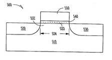
- a transistor 500 as depicted in FIG. 5may be constructed by forming a source region 520 and a drain region 530 in a silicon based substrate 510 where source and drain regions 520 , 530 are separated by a body region 532 .
- Body region 532defines a channel having a channel length 534 .
- a dielectric layeris disposed on substrate 510 .
- a gate 550is formed over and contacts gate dielectric 540 .
- the dielectric layercontains an insulating metal oxide having multiple metal species formed by atomic layer deposition in multiple layers with one or more oxygen annealings between atomic layer deposition cycles.
- the metal oxide structuremay be formed as a contiguous metal oxide film.
- the insulating metal oxideis a titanium aluminum oxide film.
- Gate dielectric 540may be realized as a dielectric layer formed substantially of a titanium aluminum oxide film. Gate dielectric 540 may be dielectric layer containing one or more layers of dielectric material in which at least one layer is titanium aluminum oxide film.
- interfacial layer 533may form between body region 532 and gate dielectric 540 .
- interfacial layer 533may be limited to a relatively small thickness compared to gate dielectric 540 , or to a thickness significantly less than gate dielectric 540 as to be effectively eliminated.
- interfacial layer 533is configured such that it is substantially without a silicon oxide layer.
- interfacial layer 533includes a silicon oxide layer having a thickness of at most four monolayers.
- interfacial layer 533includes a silicon oxide layer having a thickness of at most two monolayers. Forming the substrate, gate, and the source and drain regions may be performed using standard processes known to those skilled in the art.
- gate dielectric 540may be realized as a gate insulator in a silicon CMOS transistor.
- Use of such a gate dielectric including an insulating metal oxide film having multiple metal species formed by atomic layer deposition in a multiple layer process with one or more oxygen annealings between atomic layer deposition cyclesis not limited to silicon based substrates, but may be used with a variety of semiconductor substrates.
- FIG. 6shows an embodiment of a configuration of a floating gate transistor 600 having an insulating metal oxide having multiple metal species formed by atomic layer deposition in a multiple layer process with one or more oxygen annealings between atomic layer deposition cycles.
- the metal oxide structuremay be formed as a contiguous metal oxide film.
- the insulating metal oxideis a titanium aluminum oxide film.
- Transistor 600includes a silicon based substrate 610 with a source 620 and a drain 630 separated by a body region 632 . Body region 632 between source 620 and drain 630 defines a channel region having a channel length 634 .
- a stack 655including a gate dielectric 640 , a floating gate 652 , a floating gate dielectric 642 , and a control gate 650 .
- floating gate 652is formed over and contacts gate dielectric 640 .
- An interfacial layer 633may form between body region 632 and gate dielectric 640 .
- interfacial layer 633may be limited to a relatively small thickness compared to gate dielectric 640 , or to a thickness significantly less than gate dielectric 640 as to be effectively eliminated.
- interfacial layer 633is configured such that it is substantially without a silicon oxide layer.
- interfacial layer 633includes a silicon oxide layer having a thickness of at most four monolayers.
- interfacial layer 633includes a silicon oxide layer having a thickness of at most two monolayers.
- Gate dielectric 640includes a dielectric containing an atomic layer deposited insulating metal oxide formed in embodiments similar to those described herein.
- the metal oxideis a titanium aluminum oxide film.
- Gate dielectric 640may be realized as a dielectric layer formed substantially of titanium aluminum oxide.
- Gate dielectric 640may include multiple layers in which at least one layer is substantially titanium aluminum oxide.
- gate dielectric 640may include multiple layers where a substantially titanium aluminum oxide contacts body region 632 .
- floating gate dielectric 642includes a dielectric layer having an atomic layer deposited insulating metal oxide formed in embodiments similar to those described herein.
- Floating gate dielectric 642may be realized as a dielectric layer formed substantially of titanium aluminum oxide.
- Floating gate dielectric 642may include multiple layers in which at least one layer is substantially titanium aluminum oxide.
- control gate 650is formed over and contacts floating gate dielectric 642 .
- both gate dielectric 640 and floating gate dielectric 642may be formed as dielectric layers including an insulating metal oxide having multiple metal species formed by atomic layer deposition in a multiple layer process with one or more oxygen annealings between atomic layer deposition cycles.
- the metal oxide structuremay be formed as a contiguous metal oxide film.
- the insulating metal oxideis a titanium aluminum oxide film.
- Gate dielectric 640 , and floating gate dielectric 642may be realized by embodiments similar to those described herein with the remaining elements of the transistor 600 formed using processes known to those skilled in the art.
- gate dielectric 640forms a tunnel gate insulator and floating gate dielectric 642 forms an inter-gate insulator in flash memory devices, where gate dielectric 640 and/or floating gate dielectric 642 include an insulating metal oxide film having multiple metal species formed by atomic layer deposition in a multiple layer process with one or more oxygen annealings between atomic layer deposition cycles.
- gate dielectric 640 and floating gate dielectric 642include atomic layer deposited titanium aluminum oxide.
- Use of dielectric layers configured in various embodimentsis not limited to silicon based substrates, but may be used with a variety of semiconductor substrates.
- a methodincludes forming a first conductive layer 710 , forming a dielectric layer 720 containing an insulating metal oxide film having multiple metal species formed by atomic layer deposition on first conductive layer 710 , and forming a second conductive layer 730 on dielectric layer 720 .
- the insulating metal oxidemay be a titanium aluminum oxide film.
- Dielectric layer 720 including an insulating metal oxide film having multiple metal speciesmay be formed using any of the embodiments described herein.
- interfacial layer 715may form between first conductive layer 710 and dielectric layer 720 .
- interfacial layer 715may be limited to a relatively small thickness compared to dielectric layer 720 , or to a thickness significantly less than dielectric layer 720 as to be effectively eliminated.
- interfacial layer 715is configured such that it is substantially without a silicon oxide layer.
- interfacial layer 715includes a silicon oxide layer having a thickness of at most four monolayers.
- interfacial layer 715includes a silicon oxide layer having a thickness of at most two mono layers.
- Dielectric layer 720may be realized as a dielectric layer formed substantially of titanium aluminum oxide. Dielectric layer 720 may include multiple layers in which at least one layer is substantially titanium aluminum oxide. In an embodiment, dielectric layer 720 may include multiple layers where a substantially titanium aluminum oxide film contacts first conductive layer 710 . Embodiments for dielectric layer 720 in a capacitor includes, but is not limited to, dielectrics in DRAM capacitors and dielectrics in capacitors in analog, radio frequency (RF), and mixed signal integrated circuits.
- RFradio frequency
- a dielectric film containing an insulating metal oxide film having multiple metal species formed by atomic layer deposition in a multiple layer process with one or more oxygen annealings between atomic layer deposition cyclesmay provide for enhanced device performance by providing devices with reduced leakage current.
- improvements in leakage current characteristicsmay be attained by forming one or more layers of an atomic layer deposited titanium aluminum oxide in a nanolaminate structure with other dielectric layers including other metal oxides such as titanium oxide. The transition from one layer of the nanolaminate to another layer of the nanolaminate provides further disruption to a tendency for an ordered structure in the nanolaminate stack.
- nanolaminatemeans a composite film of ultra thin layers of two or more materials in a layered stack, where the layers are alternating layers of materials of the composite film.
- each layer in a nanolaminatehas a thickness of an order of magnitude in the nanometer range.
- each individual material layer of the nanolaminatecan have a thickness as low as a monolayer of the material or as high as 20 nanometers.
- a TiO x /TiAlO x nanolaminatecontains alternating layers of a titanium oxide and a titanium aluminum oxide.
- FIG. 8depicts a nanolaminate structure 800 for an embodiment of a dielectric structure including an insulating metal oxide film having multiple metal species formed by atomic layer deposition in a multiple layer process with one or more oxygen annealings between atomic layer deposition cycles.
- the metal oxideis a titanium aluminum oxide.
- nanolaminate structure 800includes a plurality of layers 805 - 1 , 805 - 2 to 805 -N, where at least one layer contains a titanium aluminum oxide film formed according to an embodiment herein.
- the other layersmay be other dielectric layers or dielectric metal oxides.
- the sequencing of the layersdepends on the application.
- an atomic layer deposited titanium aluminum oxide filmis the first layer formed on a substrate.
- nanolaminate structure 800contains an atomic layer deposited titanium aluminum oxide film in contact with conductive contact 810 and/or conductive contact 820 .
- the effective dielectric constant associated with nanolaminate structure 800is that attributable to N capacitors in series, where each capacitor has a thickness defined by the thickness of the corresponding layer. By selecting each thickness and the composition of each layer, a nanolaminate structure can be engineered to have a predetermined dielectric constant.
- Embodiments for structures such as nanolaminate structure 800may be used as nanolaminate dielectrics in NROM flash memory devices as well as other integrated circuits.
- Transistors, capacitors, and other devices having dielectric films containing an insulating metal oxide film having multiple metal species formed by atomic layer deposition in a multiple layer process with one or more oxygen annealings between atomic layer deposition cycles formed by the methods described abovemay be implemented into memory devices and electronic systems including information handling devices.
- Embodiments of these information handling devicesmay include wireless systems, telecommunication systems, and computers.
- embodiments of electronic devices having dielectric films containing an insulating metal oxide film having multiple metal species, such as a titanium aluminum oxide filmmay be realized as integrated circuits.
- FIG. 9illustrates a diagram for an electronic system 900 having one or more devices having a dielectric layer containing an insulating metal oxide film having multiple metal species formed by atomic layer deposition in a multiple layer process with one or more oxygen annealings between atomic layer deposition cycles fabricated according to various embodiments.
- a dielectric layerincludes a titanium aluminum oxide film.
- Electronic system 900includes a controller 905 , a bus 915 , and an electronic device 925 , where bus 915 provides electrical conductivity between controller 905 and electronic device 925 .
- controller 905 and/or electronic device 925include an embodiment for a dielectric layer an insulating metal oxide film having multiple metal species formed by atomic layer deposition as previously discussed herein.
- Electronic system 900may include, but is not limited to, information handling devices, wireless systems, telecommunication systems, fiber optic systems, electro-optic systems, and computers.
- FIG. 10depicts a diagram of an embodiment of a system 1000 having a controller 1005 and a memory 1025 .
- Controller 1005 and/or memory 1025may include a dielectric layer having an insulating metal oxide film having multiple metal species formed by atomic layer deposition in a multiple layer process with one or more oxygen annealings between atomic layer deposition cycles fabricated according to various embodiments of the present invention.
- a dielectric layerincludes a titanium aluminum oxide film.
- System 1000also includes an electronic apparatus 1035 , and a bus 1015 , where bus 1015 provides electrical conductivity between controller 1005 and electronic apparatus 1035 , and between controller 1005 and memory 1025 .
- Bus 1015may include an address, a data bus, and a control bus, each independently configured.
- bus 1015may use common conductive lines for providing address, data, and/or control, the use of which is regulated by controller 1005 .
- electronic apparatus 1035may be additional memory configured similar as memory 1025 .
- An embodimentmay include an additional peripheral device or devices 1045 coupled to bus 1015 .
- controller 1005is a processor. Any of controller 1005 , memory 1025 , bus 1015 , electronic apparatus 1035 , and peripheral device devices 1045 may include a dielectric layer including an insulating metal oxide film having multiple metal species formed according to various embodiments of the present invention. In an embodiment, such a dielectric layer includes a titanium aluminum oxide film.
- System 1000may include, but is not limited to, information handling devices, telecommunication systems, and computers.
- Peripheral devices 1045may include displays, additional storage memory, or other control devices that may operate in conjunction with controller 1005 . Alternately, peripheral devices 1045 may include displays, additional storage memory, or other control devices that may operate in conjunction with controller 1005 and/or memory 1025 .
- Memory 1025may be realized as a memory device containing a dielectric layer including an insulating metal oxide film having multiple metal species formed according to various embodiments of the present invention.
- a dielectric layerincludes a titanium aluminum oxide film. It will be understood that embodiments are equally applicable to any size and type of memory circuit and are not intended to be limited to a particular type of memory device.
- Memory typesinclude a DRAM, SRAM (Static Random Access Memory) or Flash memories.
- the DRAMcould be a synchronous DRAM commonly referred to as SGRAM (Synchronous Graphics Random Access Memory), SDRAM (Synchronous Dynamic Random Access Memory), SDRAM II, and DDR SDRAM (Double Data Rate SDRAM), as well as Synchlink or Rambus DRAMs and other emerging DRAM technologies.
- SGRAMSynchronous Graphics Random Access Memory
- SDRAMSynchronous Dynamic Random Access Memory
- SDRAM IISynchroble Data Rate SDRAM
- DDR SDRAMDouble Data Rate SDRAM
- Formation of dielectric layers containing an insulating metal oxide film having multiple metal species formed by atomic layer deposition in a multiple layer process with one or more oxygen annealings between atomic layer deposition cycles, processed in relatively low temperatures,may be amorphous and possess smooth surfaces.
- a dielectric layerincludes a titanium aluminum oxide film.
- Such titanium aluminum oxide filmscan provide enhanced electrical properties due to their smoother surface resulting in reduced leakage current.
- such dielectric layersprovide a significantly thicker physical thickness than a silicon oxide layer having the same equivalent oxide thickness, where the increased thickness would also reduce leakage current.
- Capacitors, transistors, higher level ICs or devices including memory devices, and electronic systemsare constructed utilizing the novel process for forming a dielectric film having an ultra thin equivalent oxide thickness, t eq .
- Gate dielectric layers or films including an insulating metal oxide film having multiple metal species formed by atomic layer deposition in a multiple layer process with one or more oxygen annealings between atomic layer deposition cyclesare formed having a dielectric constant ( ⁇ ) substantially higher than that of silicon oxide.
- These dielectric filmsare capable of a t eq thinner than SiO 2 gate dielectrics of the same physical thickness.
- the high dielectric constant relative to silicon dioxideallows the use of much larger physical thickness of these high- ⁇ dielectric materials for the same t eq of SiO 2 . Forming the relatively larger thickness aids in processing gate dielectrics and other dielectric layers in electronic devices and systems.
Landscapes
- Chemical & Material Sciences (AREA)
- Engineering & Computer Science (AREA)
- Chemical Kinetics & Catalysis (AREA)
- General Chemical & Material Sciences (AREA)
- Organic Chemistry (AREA)
- Metallurgy (AREA)
- Mechanical Engineering (AREA)
- Materials Engineering (AREA)
- General Physics & Mathematics (AREA)
- Power Engineering (AREA)
- Microelectronics & Electronic Packaging (AREA)
- Computer Hardware Design (AREA)
- Manufacturing & Machinery (AREA)
- Condensed Matter Physics & Semiconductors (AREA)
- Physics & Mathematics (AREA)
- Inorganic Chemistry (AREA)
- Formation Of Insulating Films (AREA)
- Semiconductor Memories (AREA)
- Insulated Gate Type Field-Effect Transistor (AREA)
- Chemical Vapour Deposition (AREA)
- Non-Volatile Memory (AREA)
Abstract
Description
- This application relates generally to semiconductor devices and device fabrication and, more particularly, to dielectric layers and their method of fabrication.
- The semiconductor device industry has a market driven need to reduce the size of devices such as transistors. To reduce transistor size, the thickness of the silicon dioxide, SiO2, gate dielectric is reduced in proportion to the shrinkage of the gate length. For example, a metal-oxide-semiconductor field effect transistor (MOSFET) would use a 1.5 nm thick SiO2gate dielectric for a gate length of 70 mm. A goal is to fabricate increasingly smaller and more reliable integrated circuits (ICs) for use in products such as processor chips, mobile telephones, and memory devices such as dynamic random access memories (DRAMs).
- Currently, the semiconductor industry relies on the ability to reduce or scale the dimensions of its basic devices, primarily, the silicon based MOSFET. This device scaling includes scaling the gate dielectric, which has primarily been fabricated using silicon dioxide. A thermally grown amorphous SiO2layer provides an electrically and thermodynamically stable material, where the interface of the SiO2layer with underlying silicon provides a high quality interface as well as superior electrical isolation properties. However, increased scaling and other requirements in microelectronic devices have created the need to use other dielectric materials as gate dielectrics.
- The abovementioned problems are addressed by the present invention and will be understood by reading and studying the following specification. An embodiment for a method for forming an electronic device includes forming a dielectric layer containing an insulating metal oxide film, in which the metal oxide includes multiple metal components formed by atomic layer deposition in a multiple layer process with one or more oxygen annealings between atomic layer deposition cycles. In an embodiment, titanium and/or aluminum is deposited in an integrated circuit on a surface of a substrate by atomic layer deposition. The deposited material is annealed using atomic oxygen. After annealing, a layer of titanium aluminum oxide is formed on the annealed material by atomic layer deposition such that a contiguous layer of titanium aluminum oxide is formed. Embodiments include structures for capacitors, transistors, memory devices, and electronic systems with dielectric layers containing an atomic layer deposited titanium aluminum oxide film, and methods for forming such structures. These and other aspects, embodiments, advantages, and features will become apparent from the following description and the referenced drawings.
FIG. 1 depicts an atomic layer deposition system for fabricating a dielectric layer containing a titanium aluminum oxide, according to various embodiments of the present invention.FIG. 2 illustrates a flow diagram of elements for an embodiment of a method to form a dielectric layer containing a titanium aluminum oxide film using atomic layer deposition, according to various embodiments of the present invention.FIG. 3 illustrates a flow diagram of elements for an embodiment of a method to form a dielectric layer containing a titanium aluminum oxide film using atomic layer deposition, according to the present invention.FIG. 4 illustrates a flow diagram of elements for an embodiment of a method to form a dielectric layer containing a titanium aluminum oxide film using atomic layer deposition, according to the present invention.FIG. 5 shows an embodiment of a configuration of a transistor having a dielectric layer containing an insulating metal oxide film having multiple metal species formed by atomic layer deposition in multiple layers with one or more oxygen annealings between atomic layer deposition cycles, according to the present invention.FIG. 6 shows an embodiment of a configuration of a floating gate transistor having a dielectric layer containing an insulating metal oxide film having multiple metal species formed by atomic layer deposition in multiple layers with one or more oxygen annealings between atomic layer deposition cycles, according to the present invention.FIG. 7 shows an embodiment of a configuration of a capacitor having a dielectric layer containing an insulating metal oxide film having multiple metal species formed by atomic layer deposition in multiple layers with one or more oxygen annealings between atomic layer deposition cycles, according to the present invention.FIG. 8 depicts an embodiment of a dielectric layer including a nanolaminate having at least one layer containing an insulating metal oxide film having multiple metal species formed by atomic layer deposition in multiple layers with one or more oxygen annealings between atomic layer deposition cycles, according to the present invention.FIG. 9 is a simplified diagram for an embodiment of a controller coupled to an electronic device having a dielectric layer containing an insulating metal oxide film having multiple metal species formed by atomic layer deposition in multiple layers with one or more oxygen annealings between atomic layer deposition cycles, according to the present invention.FIG. 10 illustrates a diagram for an embodiment of an electronic system having devices with a dielectric layer containing an insulating metal oxide film having multiple metal species formed by atomic layer deposition in multiple layers with one or more oxygen annealings between atomic layer deposition cycles, according to the present invention.- The following detailed description refers to the accompanying drawings that show, by way of illustration, specific aspects and embodiments in which the present invention may be practiced. These embodiments are described in sufficient detail to enable those skilled in the art to practice the present invention. Other embodiments may be utilized and structural, logical, and electrical changes may be made without departing from the scope of the present invention. The various embodiments disclosed herein are not necessarily mutually exclusive, as some disclosed embodiments can be combined with one or more other disclosed embodiments to form new embodiments.
- The terms wafer and substrate used in the following description include any structure having an exposed surface with which to form an integrated circuit (IC) structure. The term substrate is understood to include semiconductor wafers. The term substrate is also used to refer to semiconductor structures during processing, and may include other layers that have been fabricated thereupon. Both wafer and substrate include doped and undoped semiconductors, epitaxial semiconductor layers supported by a base semiconductor or insulator, as well as other semiconductor structures well known to one skilled in the art. The term conductor is understood to generally include n-type and p-type semiconductors and the term insulator or dielectric is defined to include any material that is less electrically conductive than the materials referred to as conductors or as semiconductors.
- The term “horizontal” as used in this application is defined as a plane parallel to the conventional plane or surface of a wafer or substrate, regardless of the orientation of the wafer or substrate. The term “vertical” refers to a direction perpendicular to the horizontal as defined above. Prepositions, such as “on”, “side” (as in “sidewall”), “higher”, “lower”, “over” and “under” are defined with respect to the conventional plane or surface being on the top surface of the wafer or substrate, regardless of the orientation of the wafer or substrate. The following detailed description is, therefore, not to be taken in a limiting sense, and the scope of the present invention is defined only by the appended claims, along with the full scope of equivalents to which such claims are entitled.
- A gate dielectric in a transistor has both a physical gate dielectric thickness and an equivalent oxide thickness (teq). The equivalent oxide thickness quantifies the electrical properties, such as capacitance, of the gate dielectric in terms of a representative physical thickness. teqis defined as the thickness of a theoretical SiO2layer that would be required to have the same capacitance density as a given dielectric, ignoring leakage current and reliability considerations.
- A SiO2layer of thickness, t, deposited on a Si surface as a gate dielectric will have a teqlarger than its thickness, t. This teqresults from the capacitance in the surface channel on which the SiO2is deposited due to the formation of a depletion/inversion region. This depletion/inversion region can result in teqbeing from 3 to 6 Angstroms (Å) larger than the SiO2thickness, t. Thus, with the semiconductor industry driving to someday scale the gate dielectric equivalent oxide thickness to under 10 Å, the physical thickness for a SiO2layer used for a gate dielectric would be need to be approximately 4 to 7 Å.
- Additional requirements on a SiO2layer would depend on the gate electrode used in conjunction with the SiO2gate dielectric. Using a conventional polysilicon gate would result in an additional increase in teqfor the SiO2layer. This additional thickness could be eliminated by using a metal gate electrode, though metal gates are not currently used in typical complementary metal-oxide-semiconductor field effect transistor (CMOS) technology. Thus, future devices would be designed towards a physical SiO2gate dielectric layer of about 5 Å or less. Such a small thickness for a SiO2oxide layer creates additional problems.
- Silicon dioxide is used as a gate dielectric, in part, due to its electrical isolation properties in a SiO2—Si based structure. This electrical isolation is due to the relatively large band gap of SiO2(8.9 eV) making it a good insulator from electrical conduction. Signification reductions in its band gap would eliminate it as a material for a gate dielectric. As the thickness of a SiO2layer decreases, the number of atomic layers, or monolayers of the material in the thickness decreases. At a certain thickness, the number of monolayers will be sufficiently small that the SiO2layer will not have a complete arrangement of atoms as in a larger or bulk layer. As a result of incomplete formation relative to a bulk structure, a thin SiO2layer of only one or two monolayers will not form a full band gap. The lack of a full band gap in a SiO2gate dielectric would cause an effective short between an underlying Si channel and an overlying polysilicon gate. This undesirable property sets a limit on the physical thickness to which a SiO2layer can be scaled. The minimum thickness due to this monolayer effect is thought to be about 7-8 Å. Therefore, for future devices to have a teqless than about 10 Å, other dielectrics than SiO2need to be considered for use as a gate dielectric.
- For a typical dielectric layer used as a gate dielectric, the capacitance is determined as one for a parallel plate capacitance: C=κ∈0A/t, where K is the dielectric constant, ∈0is the permittivity of free space, A is the area of the capacitor, and t is the thickness of the dielectric. The thickness, t, of a material is related to its teqfor a given capacitance, with SiO2having a dielectric constant κox=3.9, as
t=(κ/κox)teq=(κ/3.9)teq.
Thus, materials with a dielectric constant greater than that of SiO2, 3.9, will have a physical thickness that can be considerably larger than a desired teq, while providing the desired equivalent oxide thickness. For example, an alternate dielectric material with a dielectric constant of 10 could have a thickness of about 25.6 Å to provide a teqof 10 Å, not including any depletion/inversion layer effects. Thus, a reduced equivalent oxide thickness for transistors can be realized by using dielectric materials with higher dielectric constants than SiO2. - The thinner equivalent oxide thickness required for lower transistor operating voltages and smaller transistor dimensions may be realized by a significant number of materials, but additional fabricating requirements makes determining a suitable replacement for SiO2difficult. The current view for the microelectronics industry is still for Si based devices. This requires that the gate dielectric employed be grown on a silicon substrate or silicon layer, which places significant constraints on the substitute dielectric material. During the formation of the dielectric on the silicon layer, there exists the possibility that a small layer of SiO2could be formed in addition to the desired dielectric. The result would effectively be a dielectric layer consisting of two sublayers in parallel with each other and the silicon layer on which the dielectric is formed. In such a case, the resulting capacitance would be that of two dielectrics in series. As a result, the teqof the dielectric layer would be the sum of the SiO2thickness and a multiplicative factor of the thickness, t, of the dielectric being formed, written as
teq=tSiO2 +(κox/κ)t.
Thus, if a SiO2layer is formed in the process, the teqis again limited by a SiO2layer. In the event that a barrier layer is formed between the silicon layer and the desired dielectric in which the barrier layer prevents the formation of a SiO2layer, the teqwould be limited by the layer with the lowest dielectric constant. However, whether a single dielectric layer with a high dielectric constant or a barrier layer with a higher dielectric constant than SiO2is employed, the layer interfacing with the silicon layer must provide a high quality interface to maintain a high channel carrier mobility. - One of the advantages using SiO2as a gate dielectric has been that the formation of the SiO2layer results in an amorphous gate dielectric. Having an amorphous structure for a gate dielectric provides for reducing problems of leakage current associated with grain boundaries in polycrystalline gate dielectrics that provide high leakage paths. Additionally, grain size and orientation changes throughout a polycrystalline gate dielectric can cause variations in the film's dielectric constant, along with uniformity and surface topography problems. Typically, materials having the advantage of a high dielectric constant relative to SiO2also have the disadvantage of a crystalline form, at least in a bulk configuration. The best candidates for replacing SiO2as a gate dielectric are those with high dielectric constant, which can be fabricated as a thin layer with an amorphous form.
- High-κ materials include materials having a dielectric constant greater than silicon dioxide, for example, dielectrics materials having a dielectric constant greater than about twice the dielectric constant of silicon dioxide. Examples of such high-κ materials include Ta2O3, TiO2, Al2O3, ZrO2, Y2O3, ZrSixOy, HfSixOy, and barium strontium titanate (BST). An appropriate high-κ gate dielectric to replace SiO2should have a large energy gap (Eg) and large energy barrier heights with Si for both electrons and holes. Generally, the bandgap is inversely related to the dielectric constant for a high-κ material, which lessens some advantages of the high-κ material. Dielectric layers of titanium aluminum oxide offer a material that can provide a relatively high dielectric constant with respect to silicon oxide and an acceptably high bandgap. The dielectric constant and bandgap for titanium aluminum oxide will range in value from that of Al2O3to that of TiO2. Al2O3has a bandgap of about 8.7 eV and a dielectric constant of about 9, while TiO2has a bandgap of about 3.5 eV and a dielectric constant of about 80. Engineering a titanium aluminum oxide film can provide dielectric layers for electronic devices with dielectric constants of about 30 with bandgaps of about 4 eV.
- Other characteristics for choosing a silicon oxide replacement include using materials that provide a sharp interface with silicon that may provide a low density of interface states, a large energy barrier from the conduction band to the Fermi level of the gate electrode to maintain leakage current at acceptable levels, and structural stability with contact electrodes and substrate material during device processing steps performed after providing the dielectric layer.
- Embodiments for forming a titanium aluminum oxide film by atomic layer deposition may provide a film having a specific stoichiometry or it may be a non-stoichiometric titanium aluminum oxide. The expression TiAlOxis used herein to represent a stoichiometric and/or a non-stoichiometric titanium aluminum oxide. Embodiments of dielectric layers containing an atomic layer deposited titanium aluminum oxide layer have a larger dielectric constant than silicon dioxide. Such dielectric layers provide a significantly thinner equivalent oxide thickness compared with a silicon oxide layer having the same physical thickness. Alternately, such dielectric layers provide a significantly thicker physical thickness than a silicon oxide layer having the same equivalent oxide thickness. This increased physical thickness aids in reducing leakage current.
- Another consideration for selecting the material and method for forming a dielectric layer for use in electronic devices and systems concerns the roughness of a dielectric layer on a substrate. Surface roughness of the dielectric layer has a significant effect on the electrical properties of the gate oxide, and the resulting operating characteristics of the transistor. The leakage current through a physical 1.0 nm gate oxide increases by a factor of 10 for every 0.1 increase in the root-mean-square (RMS) roughness.
- During a conventional sputtering deposition process stage, particles of the material to be deposited bombard the surface at a high energy. When a particle hits the surface, some particles adhere, and other particles cause damage. High energy impacts remove body region particles creating pits. The surface of such a deposited layer can have a rough contour due to the rough interface at the body region.
- In an embodiment, a titanium aluminum oxide dielectric layer having a substantially smooth surface relative to other processing techniques is formed using atomic layer deposition (ALD). Further, forming such a dielectric layer using atomic layer deposition can provide for controlling transitions between material layers. Thus, atomic layer deposited titanium aluminum oxide dielectric layers can have an engineered transition with a substrate surface.
- ALD, also known as atomic layer epitaxy (ALE), is a modification of chemical vapor deposition (CVD) and is also called “alternatively pulsed-CVD.” In ALD, gaseous precursors are introduced one at a time to the substrate surface mounted within a reaction chamber (or reactor). This introduction of the gaseous precursors takes the form of pulses of each gaseous precursor. In a pulse of a precursor gas, the precursor gas is made to flow into a specific area or region for a short period of time. Between the pulses, the reaction chamber is purged with a gas, which in many cases is an inert gas, and/or evacuated.
- In a chemisorption-saturated ALD (CS-ALD) process, during the first pulsing phase, reaction with the substrate occurs with the precursor saturatively chemisorbed at the substrate surface. Subsequent pulsing with a purging gas removes precursor excess from the reaction chamber.
- The second pulsing phase introduces another precursor on the substrate where the growth reaction of the desired film takes place. Subsequent to the film growth reaction, reaction byproducts and precursor excess are purged from the reaction chamber. With favourable precursor chemistry where the precursors adsorb and react with each other on the substrate aggressively, one ALD cycle can be preformed in less than one second in properly designed flow type reaction chambers. Typically, precursor pulse times range from about 0.5 sec to about 2 to 3 seconds.
- In ALD, the saturation of all the reaction and purging phases makes the growth self-limiting. This self-limiting growth results in large area uniformity and conformality, which has important applications for such cases as planar substrates, deep trenches, and in the processing of porous silicon and high surface area silica and alumina powders. Significantly, ALD provides for controlling film thickness in a straightforward manner by controlling the number of growth cycles.
- ALD was originally developed to manufacture luminescent and dielectric layers needed in electroluminescent displays. Significant efforts have been made to apply ALD to the growth of doped zinc sulfide and alkaline earth metal sulfide films. Additionally, ALD has been studied for the growth of different epitaxial II-V and II-VI films, nonepitaxial crystalline or amorphous oxide and nitride films and multilayer structures of these. There also has been considerable interest towards the ALD growth of silicon and germanium films, but due to the difficult precursor chemistry, this has not been very successful.
- The precursors used in an ALD process may be gaseous, liquid or solid. However, liquid or solid precursors should be volatile. The vapor pressure should be high enough for effective mass transportation. Also, solid and some liquid precursors may need to be heated inside the reaction chamber and introduced through heated tubes to the substrates. The necessary vapor pressure should be reached at a temperature below the substrate temperature to avoid the condensation of the precursors on the substrate. Due to the self-limiting growth mechanisms of ALD, relatively low vapor pressure solid precursors can be used though evaporation rates may somewhat vary during the process because of changes in their surface area.
- There are several other characteristics for precursors used in ALD. The precursors should be thermally stable at the substrate temperature because their decomposition would destroy the surface control and accordingly the advantages of the ALD method that relies on the reaction of the precursor at the substrate surface. A slight decomposition, if slow compared to the ALD growth, can be tolerated.
- The precursors should chemisorb on or react with the surface, though the interaction between the precursor and the surface as well as the mechanism for the adsorption is different for different precursors. The molecules at the substrate surface should react aggressively with the second precursor to form the desired solid film. Additionally, precursors should not react with the film to cause etching, and precursors should not dissolve in the film. Using highly reactive precursors in ALD contrasts with the selection of precursors for conventional CVD.
- The by-products in the reaction should be gaseous in order to allow their easy removal from the reaction chamber. Further, the by-products should not react or adsorb on the surface.
- In a reaction sequence ALD (RS-ALD) process, the self-limiting process sequence involves sequential surface chemical reactions. RS-ALD relies on chemistry between a reactive surface and a reactive molecular precursor. In an RS-ALD process, molecular precursors are pulsed into the ALD reaction chamber separately. The metal precursor reaction at the substrate is typically followed by an inert gas pulse to remove excess precursor and by-products from the reaction chamber prior to pulsing the next precursor of the fabrication sequence.
- By RS-ALD, films can be layered in equal metered sequences that are all identical in chemical kinetics, deposition per cycle, composition, and thickness. RS-ALD sequences generally deposit less than a full layer per cycle. Typically, a deposition or growth rate of about 0.25 to about 2.00 Å per RS-ALD cycle can be realized.
- The advantages of RS-ALD include continuity at an interface avoiding poorly defined nucleating regions that are typical for chemical vapor deposition (<20 Å) and physical vapor deposition (<50 Å), conformality over a variety of substrate topologies due to its layer-by-layer deposition technique, use of low temperature and mildly oxidizing processes, lack of dependence on the reaction chamber, growth thickness dependent solely on the number of cycles performed, and ability to engineer multilayer laminate films with resolution of one to two monolayers. RS-ALD processes allows for deposition control on the order on monolayers and the ability to deposit monolayers of amorphous films.
- Herein, a sequence refers to the ALD material formation based on an ALD reaction of one precursor with its reactant precursor. For example, forming titanium oxide from a TiI4precursor and H2O2, as its reactant precursor, forms an embodiment of a titanium/oxygen sequence, which can also be referred to as titanium sequence. A cycle of a sequence includes pulsing a precursor, pulsing a purging gas for the precursor, pulsing a reactant precursor, and pulsing the reactant's purging gas. However, in forming a layer of a metal species, an ALD sequence deals with reacting a precursor containing the metal species with a substrate surface. A cycle for such a metal forming sequence includes pulsing a purging gas after pulsing the precursor containing the metal species. In an embodiment, a layer of titanium aluminum oxide is formed on a substrate mounted in a reaction chamber using ALD in repetitive titanium and aluminum sequences using precursor gases individually pulsed into the reaction chamber. Alternately, solid or liquid precursors can be used in an appropriately designed reaction chamber.
FIG. 1 shows an embodiment of an atomiclayer deposition system 100 for processing a dielectric layer containing an insulating metal oxide film having multiple metal species, such as a titanium aluminum oxide film, constructed in a multiple layer process with one or more oxygen annealings between atomic layer deposition cycles. The elements depicted permit discussion of the present invention such that those skilled in the art may practice the present invention without undue experimentation. InFIG. 1 , asubstrate 110 is located inside areaction chamber 120 ofALD system 100. Also located within thereaction chamber 120 is a heating element130, which is thermally coupled tosubstrate 110 to control the substrate temperature. A gas-distribution fixture 140 introduces precursor gases to thesubstrate 110. Each precursor gas originates from individual gas sources151-154 whose flow is controlled by mass-flow controllers156-159, respectively. Gas sources151-154 provide a precursor gas either by storing the precursor as a gas or by providing a location and apparatus for evaporating a solid or liquid material to form the selected precursor gas.- Also included in the ALD system are purging
gas sources flow controllers ALD system 100, one purging gas source for each precursor gas, for example. For a process that uses the same purging gas for multiple precursor gases less purging gas sources are required forALD system 100. Gas sources151-154 and purging gas sources161-162 are coupled by their associated mass-flow controllers to a common gas line orconduit 170, which is coupled to the gas-distribution fixture 140 inside thereaction chamber 120.Gas conduit 170 is also coupled to vacuum pump, or exhaust pump,181 by mass-flow controller 186 to remove excess precursor gases, purging gases, and by-product gases at the end of a purging sequence from the gas conduit. - Vacuum pump, or exhaust pump,182 is coupled by mass-
flow controller 187 to remove excess precursor gases, purging gases, and by-product gases at the end of a purging sequence fromreaction chamber 120. For convenience, control displays, mounting apparatus, temperature sensing devices, substrate maneuvering apparatus, and necessary electrical connections as are known to those skilled in the art are not shown inFIG. 1 . ThoughALD system 100 is well suited for practicing the present invention, other ALD systems commercially available can be used. - The use, construction and fundamental operation of reaction chambers for deposition of films are understood by those of ordinary skill in the art of semiconductor fabrication. The present invention man be practiced on a variety of such reaction chambers without undue experimentation. Furthermore, one of ordinary skill in the art will comprehend the necessary detection, measurement, and control techniques in the art of semiconductor fabrication upon reading the disclosure.
- The elements of
ALD system 100 can be controlled by a computer. To focus on the use ofALD system 100 in the various embodiments of the present invention, the computer is not shown. Those skilled in the art can appreciate that the individual elements such as pressure control, temperature control, and gas flow withinALD system 100 can be under computer control. - In an embodiment, a method for forming a dielectric layer includes forming an insulating metal oxide having multiple metal species. The method of forming the insulating metal oxide includes forming a first layer of a first metal and/or a second metal by atomic layer deposition. In an embodiment, the first layer is formed having a thickness that is at most substantially two monolayers. In an embodiment, the first layer may be formed having one of the multiple metals with the remaining one or more metals incorporated into the first layer on subsequent processing. In an embodiment, a first layer formed with one metal species may have a thickness ranging from one to two monolayers.
- After forming the first layer of metal, the first layer is annealed using oxygen. The oxygen may be substantially atomic oxygen, substantially molecular oxygen, or may include atomic oxygen and molecular oxygen. With one metal species formed as a thin first layer, deposition of the other metals to form the desired insulating metal oxide may be concluded by atomic layer deposition following the annealing to form the initial first layer as a first layer of the desired insulating metal oxide. Such a subsequently formed metal oxide having multiple metal species may be further annealed using oxygen.
- After annealing the fist layer, a second layer of an insulating metal oxide having the multiple metal species is formed onto the first layer by atomic layer deposition to form a contiguous layer. The second layer of insulating metal oxide may be formed in a manner similar to forming and annealing the first layer. In an embodiment, the second layer of insulating metal oxide containing multiple metal species is constructed by forming a number of layers by atomic layer deposition with a number of oxygen annealings between atomic layer deposition cycles and between layer formation. The completed annealed first layer and second layer provides one contiguous insulating metal oxide having multiple metal species. In an embodiment, the insulating metal oxide is a titanium aluminum oxide film.
FIG. 2 illustrates a flow diagram of elements for an embodiment of a method to form a dielectric layer containing a titanium aluminum oxide film. At210, titanium and/or aluminum are deposited onto a substrate surface by atomic layer deposition to form a first layer. The first layer may be formed to provide uniform coverage of the desired area of the substrate surface for forming the dielectric layer to avoid forming a silicon oxide in an interface between the substrate surface and the dielectric layer. A number of precursors containing titanium may be used to deposit the titanium and a number of precursors containing aluminum may be used to deposit the aluminum. In an embodiment, titanium is deposited before aluminum. In an embodiment, aluminum is deposited before titanium. Alternately, titanium and aluminum may be jointly deposited using precursors that substantially do no react with each other, but react at the substrate surface. In an embodiment, one of either titanium or aluminum may be deposited by atomic layer deposition with the other metal deposited at a later stage of the process for forming the titanium aluminum oxide film. In embodiment, the deposited titanium and/or aluminum form one or more monolayers over the desired area of the substrate surface for forming the dielectric layer. In embodiment, titanium is deposited over a portion of the desired area of the substrate surface for forming the dielectric layer with aluminum deposited over the remaining portion of the desired area. Such partial coverage can be realized by pulsing a titanium precursor for a pulsing period that provides the partial coverage of a monolayer on the surface and then pulsing an aluminum precursor provides uniform formation of a monolayer over the surface including the surface having deposited titanium. Alternately, the aluminum precursor may be pulsed prior to the titanium precursor.- At220, the first layer is annealed using oxygen. In an embodiment, oxygen annealing is conducted after depositing one of titanium and aluminum and again after depositing the other one of titanium and aluminum. Such oxygen annealing following individual deposition of aluminum and titanium may be conducted after forming a monolayer of each metal. In an embodiment, the oxygen used is atomic oxygen. In an embodiment, the oxygen used is molecular oxygen. Alternately, the oxygen includes a combination of atomic and molecular oxygen. The annealing of the first layer provides for forming the first layer as a titanium aluminum oxide layer in which an interface, between the first layer and the substrate surface on which it is deposited, is substantially without a silicon oxide layer or has a silicon oxide layer having a thickness of at most two monolayers. In other embodiments, a silicon oxide layer having a thickness of at most four monolayers is formed in the interface. Titanium and aluminum have oxide formation energies that are more negative than silicon, and as a result, the formation of the first layer having titanium and/or aluminum on the surface with a silicon substrate will reduce the likelihood for formation of interfacial silicon oxide. Using atomic oxygen may provide lower leakage current than using molecular oxygen. Using atomic oxygen may also provide a smaller amount of interfacial silicon oxide than using molecular oxygen. In an embodiment, after annealing a deposited layer of one of either titanium or aluminum, metal atoms of either titanium or aluminum not deposited before annealing are deposited to form the first layer as a TiAlOxlayer.
- At230, after annealing the first layer, a second layer of titanium aluminum oxide is formed onto the first layer by atomic layer deposition to form a contiguous titanium aluminum oxide layer. The second layer may be formed in a similar deposition and annealing manner as the first layer. Alternately, the second layer may be formed as multiple contiguous TiAlOxlayers, each layer formed in a manner similar to forming the first TiAlOxlayer. In an embodiment, the second titanium aluminum oxide layer is formed by atomic layer deposition using a titanium/oxide sequence and an aluminum/oxide sequence. Alternately, the second layer may be formed as multiple contiguous TiAlOxlayers, each layer formed by atomic layer deposition using a titanium/oxide sequence and an aluminum/oxide sequence with an oxygen annealing conducted in between forming each layer. In an embodiment, the second titanium aluminum oxide layer may be formed as multiple contiguous layers having a number of oxygen annealings performed between selected ALD cycles or between selected layers. Further, a multi-layered process for the second TiAlOx layer may have a number of layers formed in a manner similar to the first layer and a number of layers formed using a selected permutation of titanium/oxide and an aluminum/oxide ALD sequences. After forming the titanium aluminum film, other dielectric layers such as nitride layers and/or insulating metal oxide layers may be formed as part of the dielectric layer. The dielectric layer may be formed as a nanolaminate. An embodiment of a nanolaminate may include a layer of titanium oxide and the titanium aluminum oxide film. Alternately, the dielectric layer may be formed substantially as the titanium aluminum oxide film.
- In various embodiments, the structure of the interface between the dielectric layer and the substrate on which it is disposed is controlled to limit the inclusion of silicon oxide, since a silicon oxide layer would reduce the effective dielectric constant of the dielectric layer. The material composition and its properties for an interface layer are typically dependent on process conditions and the condition of the substrate before forming the dielectric layer. Though the existence of an interface layer may effectively reduce the dielectric constant associated with the dielectric layer and its substrate interface layer, a silicon oxide interface layer or other composition interface layer, may improve the interface density, fixed charge density, and channel mobility of a device having this interface layer.
FIG. 3 illustrates a flow diagram of elements for an embodiment of a method to form a dielectric layer containing a titanium aluminum oxide film. At310, a layer of titanium aluminum oxide is formed by atomic layer deposition to provide a first layer. The TiAlOxlayer may be formed using a number of cycles having various permutations of titanium/oxide sequences and aluminum/oxide sequences. A number of titanium containing precursors and a number of oxygen containing precursors may be used in the titanium sequences. A number of aluminum containing precursors and a number of oxygen containing precursors may be used in the aluminum sequences. In an embodiment, the initial ALD sequence is conducted with a pulsing period sufficient to provide metal, aluminum or titanium, coverage uniformly over the desired area of the substrate surface on which the dielectric is being formed. In an embodiment, the initial ALD sequence is a combination of titanium and aluminum sequences conducted with a pulsing period sufficient to provide aluminum and titanium coverage uniformly over the desired area of the substrate surface on which the dielectric is being formed. In an embodiment, the combination sequence does not use titanium precursors and aluminum precursors that interact with each other but react with the substrate surface to deposit titanium and aluminum.- At320, the first layer of titanium aluminum is annealed using oxygen. In an embodiment, annealing is conducted with the first layer formed as a monolayer. In an embodiment, annealing is conducted with the first layer formed as at most five monolayers. Oxygen annealing may be conducted for thin layers of the first layer to aid in the formation of the TiAlOxfirst layer maintaining an interface with the substrate surface that has a silicon oxide interfacial layer of at most four monolayers. In an embodiment, the interface may be formed substantially without interfacial silicon oxide. In an embodiment, the annealing oxygen is essentially atomic oxygen. In an embodiment, the annealing oxygen is essentially molecular oxygen. Alternately, the annealing oxygen includes a combination of atomic and molecular oxygen. Using atomic oxygen may provide lower leakage current than using molecular oxygen. Using atomic oxygen may also provide a smaller amount of interfacial silicon oxide than using molecular oxygen.
- At330, after annealing the first layer, a second layer of titanium aluminum oxide is formed onto the first layer by atomic layer deposition to form a contiguous titanium aluminum oxide layer. The second layer may be formed in a similar deposition and annealing manner as the first layer, at310 and320. Alternately, the second layer may be formed as multiple contiguous TiAlOxlayers, each layer formed in a manner similar to forming the first TiAlOxlayer. Alternately, the second layer may be formed as multiple contiguous TiAlOxlayers, each layer formed by atomic layer deposition using a titanium/oxide sequence and an aluminum/oxide sequence with an oxygen annealing conducted in between forming each layer. In an embodiment, the second titanium aluminum oxide layer may be formed as multiple contiguous layers having a number of oxygen annealings performed between selected ALD cycles or between selected layers. Further, a multi-layered process for the second TiOx layer may have a number of layers formed using a selected permutation of titanium/oxide and an aluminum/oxide ALD sequences. After forming the titanium aluminum film, other dielectric layers such as nitride layers and/or insulating metal oxide layers may be formed as part of the dielectric layer. The dielectric layer may be formed as a nanolaminate. An embodiment of a nanolaminate may include a layer of titanium oxide and the titanium aluminum oxide film. Alternately, the dielectric layer may be formed substantially as the titanium aluminum oxide film.
- In the various embodiments, the thickness of TiAlOxfilm is related to the number of ALD cycles performed for each metal species and the growth rate associated with the selected permutations of sequences in the cycles. As can be understood by those skilled in the art, particular effective growth rates for the engineered TiAlOxfilm can be determined during normal initial testing of the ALD system for processing a titanium aluminum oxide dielectric for a given application without undue experimentation.
- Atomic layer deposition of the individual components of the titanium aluminum oxide layer allows for individual control of each precursor pulsed into the reaction chamber. Thus, each precursor is pulsed into the reaction chamber for a predetermined period, where the predetermined period can be set separately for each precursor. Additionally, for various embodiments for ALD formation of a titanium aluminum oxide layer, each precursor can be pulsed into the reaction under separate environmental conditions. The substrate can be maintained at a selected temperature and the reaction chamber maintained at a selected pressure independently for pulsing each precursor. Appropriate temperatures and pressures may be maintained, whether the precursor is a single precursor or a mixture of precursors. During atomic layer deposition, the pulsing of the precursor gases is separated by purging the reaction chamber with a purging gas following each pulsing of a precursor. In an embodiment, nitrogen gas is used as the purging gas following the pulsing of each precursor used in a cycle to form a film of titanium aluminum oxide. Additionally, the reaction chamber can also be purged by evacuating the reaction chamber.
FIG. 4 illustrates a flow diagram of elements for an embodiment of a method to form a dielectric layer containing a titanium aluminum oxide film using atomic layer deposition. This embodiment can be implemented with the atomiclayer deposition system 100 ofFIG. 1 . At410, asubstrate 110 is prepared. The substrate used for forming a integrated circuit is typically a silicon or silicon containing material. In other embodiments, germanium, gallium arsenide, silicon-on-sapphire substrates, or other suitable substrates may be used. This preparation process includes cleaningsubstrate 110 and forming layers and regions of the substrate, such as drains and sources of a metal oxide semiconductor (MOS) transistor, prior to forming a gate dielectric. Alternately, these active regions may be formed after forming the dielectric layer, depending on the over-all fabrication process implemented. In an embodiment, the substrate is cleaned to provide an initial substrate depleted of its native oxide. In an embodiment, the initial substrate is cleaned to also provide a hydrogen-terminated surface. In an embodiment, a silicon substrate undergoes a final hydrofluoric (HF) rinse prior to ALD processing to provide the silicon substrate with a hydrogen-terminated surface without a native silicon oxide layer.- Cleaning immediately preceding atomic layer deposition aids in reducing an occurrence of silicon oxide as an interface between a silicon based substrate and a dielectric formed using the atomic layer deposition process. The material composition and its properties of an interface layer are typically dependent on process conditions and the condition of the substrate before forming the dielectric layer. Though the existence of an interface layer may effectively reduce the dielectric constant associated with the dielectric layer and its substrate interface layer, a SiO2interface layer or other composition interface layer, may improve the interface density, fixed charge density, and channel mobility of a device having this interface layer.
- The sequencing of the formation of the regions of the transistor being processed follows typical sequencing that is generally performed in the fabrication of a MOS transistor as is well known to those skilled in the art. Included in the processing prior to forming a gate dielectric is the masking of substrate regions to be protected during the gate dielectric formation, as is typically performed in MOS fabrication. In this embodiment, the unmasked region includes a body region of a transistor, however one skilled in the art will recognize that other semiconductor device structures may utilize this process. Additionally, the
substrate 110 in its ready for processing form is conveyed into a position inreaction chamber 120 for ALD processing. - At415, a titanium precursor is pulsed into
reaction chamber 120. In an embodiment, TiI4is used as a precursor. The TiI4is pulsed intoreaction chamber 120 through the gas-distribution fixture 140 ontosubstrate 110. The flow of the TiI4is controlled by mass-flow controller 156 fromgas source 151. In embodiment, the substrate temperature is maintained between about 300° C. and about 400° C. by heating element130 for a TiI4precursor. In another embodiment, a TiCl4precursor is used with the substrate temperature maintained between about 425° C. and about 600° C. Other titanium precursors may be used. The titanium precursor reacts with the surface of thesubstrate 110 in the desired region defined by the unmasked areas of thesubstrate 110. In various embodiments, the presence of residual chlorine in a titanium aluminum oxide dielectric layer may be reduced or eliminated providing a substantially chlorine free film by using metal precursors other than metal chlorides in the ALD processing of each metal, titanium and aluminum. Use of a metal iodine as a precursor results in a film substantially free of residual iodine. As a result, metal halide precursors other than chloride metal precursors may be used. Eliminating residual chloride in such dielectric layers may provide reduced leakage current for devices having these dielectric layers. - At420, a first purging gas is pulsed into the
reaction chamber 120. In an embodiment, nitrogen is used as a purging gas and a carrier gas. The nitrogen flow is controlled by mass-flow controller 166 from the purginggas source 161 into thegas conduit 170. Using the pure nitrogen purge avoids overlap of the precursor pulses and possible gas phase reactions. Following the purge, a first reactant precursor is pulsed into thereaction chamber 120, at425. - For the titanium sequence using TiI4as the precursor, oxygen precursor, H2O2, may be used as the reactant precursor. For a titanium sequence using TiCl4as the precursor, oxygen precursor, H2O, may be used as the reactant precursor. The reactant precursor is pulsed into the
reaction chamber 120 throughgas conduit 170 fromgas source 152 by mass-flow controller 157. The reactant precursor aggressively reacts at the surface ofsubstrate 110. - Following the pulsing of a first reactant precursor, a second purging gas is injected into the
reaction chamber 120, at430. Nitrogen gas is used to purge the reaction chamber after pulsing each precursor gas in a titanium/oxygen sequence. Excess precursor gas, and reaction by-products are removed from the system by the purge gas in conjunction with the exhausting of thereaction chamber 120 usingvacuum pump 182 through mass-flow controller 187, and exhausting of thegas conduit 170 by thevacuum pump 181 through mass-flow controller 186. - At435, an aluminum precursor is pulsed into
reaction chamber 120. In an embodiment, the aluminum precursor is trimethyl aluminum. Other aluminum precursors may be used. In an embodiment, the substrate temperature is maintained between about 300° C. and a pressure of about 1 Torr. Mass-flow controller 158 regulates the pulsing of the aluminum precursor to the surface of thesubstrate 110 through gas-distribution fixture 140 fromgas source 153. - At440, a third purging gas is introduced into the system. Nitrogen gas can also be used as a purging and carrier gas. The nitrogen flow is controlled by mass-
flow controller 167 from the purginggas source 162 into thegas conduit 170 and subsequently into thereaction chamber 120. In another embodiment, argon gas is used as the purging gas. Following the pulsing of the third purging gas, a second reactant precursor is pulsed into thereaction chamber 120, at445. The reactant precursor is selected to produce an oxidizing reaction for the aluminum at the substrate surface. In an embodiment, the reactant precursor is H2O vapor. Mass-flow controller 159 regulates the water vapor pulsing intoreaction chamber 120 throughgas conduit 170 fromgas source 154. The H2O vapor aggressively reacts at the surface ofsubstrate 110. - Following the pulsing of the second reactant precursor, a fourth purging gas is injected into
reaction chamber 120, at450. Nitrogen gas may be used to purge the reaction chamber after pulsing each precursor gas in the aluminum/oxygen sequence. In another embodiment, argon gas may be used as the purging gas. Excess precursor gas, and reaction by-products are removed from the system by the purge gas in conjunction with the exhausting ofreaction chamber 120 usingvacuum pump 182 through mass-flow controller 187, and exhausting of thegas conduit 170 by thevacuum pump 181 through mass-flow controller 186. - At455, titanium sequences and aluminum sequences are repeated for a number of cycles to form a first layer of titanium aluminum oxide. In an embodiment, the number of cycles is selected to provide a first layer of titanium aluminum oxide having a thickness of about one to two monolayers. In an embodiment, the number of cycles is selected to provide a first layer of titanium aluminum oxide having a thickness of at most four monolayers. In an embodiment, a titanium/aluminum cycle may include permutations of a number of titanium sequences with a number of aluminum sequences.
- At460, the titanium aluminum layer is annealed using oxygen. The annealing may be conducted at 500° C. The annealing may be conducted as a room temperature exposure to oxygen. In an embodiment, the annealing oxygen is substantially atomic oxygen. In another embodiment, the annealing oxygen is substantially molecular oxygen. Alternately, the annealing oxygen includes atomic oxygen and molecular oxygen.
- At465, titanium sequences and aluminum sequences are repeated for a number of cycles to form a second titanium aluminum oxide layer onto the first layer of titanium aluminum oxide. The two layers form a contiguous titanium aluminum oxide layer.
- At470, determination is made as to whether the desired thickness for the titanium aluminum oxide film has been formed. The desired thickness is related to the number of ALD cycles to form the sublayers of the titanium aluminum oxide film. If the number of completed cycles is less than the number needed to form the desired thickness for the titanium aluminum oxide film, additional ALD processing is conducted. Prior to performing additional ALD processing, a determination is made, at375, as to whether additional annealing is desired. If additional annealing is desired, the process continues at460. In various embodiments, a number of oxygen annealing procedures may be implemented between the ALD cycles. If no additional annealing is desired, the process continues at465.
- The thickness of a titanium aluminum oxide film is determined by a fixed growth rate for the pulsing periods and precursors used, set at a value such as N nm/combined cycle, dependent upon the number of cycles of the aluminum sequence relative to the titanium sequence that form a combined sequence. For a desired titanium aluminum oxide film thickness, t, in an application such as forming a gate dielectric of a MOS transistor, the ALD process is repeated for t/N total combined cycles. Once the t/N cycles have completed, no further ALD processing for titanium aluminum oxide is required.
- At480, after forming the desired thickness for the titanium aluminum oxide film, the process continues with completing device fabrication. Further processing of the device may include annealing a device structure that includes the dielectric layer. Such annealing may aid in reducing leakage current through the dielectric layer containing the titanium aluminum film. The titanium aluminum oxide film processed at these relatively low temperatures may provide an amorphous dielectric layer. In an embodiment, completing the device includes completing the formation of a transistor. In another embodiment, completing the device includes completing the formation of a capacitor. Alternately, completing the process includes completing the construction of a memory device having an array with access transistors formed with gate dielectrics containing atomic layer deposited titanium aluminum oxide. Further, in another embodiment, completing the process includes the formation of an electronic system including an information handling device that uses electronic devices with transistors formed with dielectric layers containing atomic layer deposited titanium aluminum oxide. Typically, information handling devices such as computers include many memory devices, having many access transistors.
- It can appreciated by those skilled in the art that the elements of a method for forming an atomic layer deposited titanium aluminum oxide film in the embodiment of
FIG. 4 can be performed with various number of titanium sequences relative to the number of aluminum sequences. In selecting the number of titanium sequences and aluminum sequences relative to each other, a titanium aluminum oxide film can be engineering with bandgap and dielectric constant characteristics ranging from that of Al2O3to that of TiO2. In another embodiment, the ALD processing of a titanium aluminum oxide dielectric layer may provide a dielectric layer having a dielectric constant of about 30. In various embodiments, a dielectric layer of titanium aluminum oxide is provided such that a interface between the dielectric layer and a substrate surface on which it is disposed has substantially no silicon oxide layer or a silicon oxide layer of at most two monolayers thickness. The selection of the dielectric constant may be conducted in a optimization, or trade-off, process with improving the current leakage characteristics of the film. - The embodiments described herein provide a process for growing a dielectric layer having a wide range of useful equivalent oxide thickness, teq, associated with a dielectric constant in the range from about 9 to about 80. The lower end of this range is associated with a titanium aluminum oxide film that is aluminum rich. For example, an aluminum rich film but may viewed as an aluminum oxide film doped with titanium. The upper end of the range for a titanium aluminum film is associated with a titanium aluminum oxide film that is titanium rich. For example, an titanium rich film but may viewed as a titanium oxide film doped with aluminum. For a titanium aluminum film with the amount of titanium and aluminum in approximately equal proportions, the dielectric constant is about 30. A dielectric constant of about 30 provides for a teqthat is about 13% of a given silicon dioxide thickness. In an embodiment, a dielectric layer containing a atomic layer deposited titanium aluminum oxide film has a teqthat is less than 10 Å. In an embodiment, a dielectric layer containing a atomic layer deposited titanium aluminum oxide film has a teqthat is less than 3 Å. Alternately, for an acceptable silicon dioxide thickness, an embodiment for a titanium aluminum oxide with a dielectric constant of about 30 may be about seven to eight times larger than the acceptable silicon dioxide thickness providing enhanced probability for reducing leakage current. Further, dielectric layers of titanium aluminum oxide formed in various embodiments may provide not only thin teqfilms, but also amorphous films with relatively low leakage current. Additionally, the novel process can be implemented to form transistors, capacitors, memory devices, and other electronic systems including information handling devices.
- A
transistor 500 as depicted inFIG. 5 may be constructed by forming asource region 520 and adrain region 530 in a silicon basedsubstrate 510 where source and drainregions body region 532.Body region 532 defines a channel having achannel length 534. A dielectric layer is disposed onsubstrate 510. Agate 550 is formed over andcontacts gate dielectric 540. The dielectric layer contains an insulating metal oxide having multiple metal species formed by atomic layer deposition in multiple layers with one or more oxygen annealings between atomic layer deposition cycles. The metal oxide structure may be formed as a contiguous metal oxide film. In an embodiment, the insulating metal oxide is a titanium aluminum oxide film. The dielectric is formed onsubstrate 510. The resulting dielectric layer formsgate dielectric 540.Gate dielectric 540 may be realized as a dielectric layer formed substantially of a titanium aluminum oxide film.Gate dielectric 540 may be dielectric layer containing one or more layers of dielectric material in which at least one layer is titanium aluminum oxide film. - An
interfacial layer 533 may form betweenbody region 532 andgate dielectric 540. In an embodiment,interfacial layer 533 may be limited to a relatively small thickness compared togate dielectric 540, or to a thickness significantly less than gate dielectric540 as to be effectively eliminated. In an embodiment,interfacial layer 533 is configured such that it is substantially without a silicon oxide layer. In an embodiment,interfacial layer 533 includes a silicon oxide layer having a thickness of at most four monolayers. In an embodiment,interfacial layer 533 includes a silicon oxide layer having a thickness of at most two monolayers. Forming the substrate, gate, and the source and drain regions may be performed using standard processes known to those skilled in the art. Additionally, the sequencing of the various elements of the process for forming a transistor may be conducted with standard fabrication processes, also as known to those skilled in the art. In an embodiment,gate dielectric 540 may be realized as a gate insulator in a silicon CMOS transistor. Use of such a gate dielectric including an insulating metal oxide film having multiple metal species formed by atomic layer deposition in a multiple layer process with one or more oxygen annealings between atomic layer deposition cycles is not limited to silicon based substrates, but may be used with a variety of semiconductor substrates. FIG. 6 shows an embodiment of a configuration of a floatinggate transistor 600 having an insulating metal oxide having multiple metal species formed by atomic layer deposition in a multiple layer process with one or more oxygen annealings between atomic layer deposition cycles. The metal oxide structure may be formed as a contiguous metal oxide film. In an embodiment, the insulating metal oxide is a titanium aluminum oxide film.Transistor 600 includes a silicon basedsubstrate 610 with asource 620 and adrain 630 separated by abody region 632.Body region 632 betweensource 620 and drain630 defines a channel region having achannel length 634. Located abovebody region 632 is astack 655 including agate dielectric 640, a floatinggate 652, a floatinggate dielectric 642, and acontrol gate 650. In an embodiment, floatinggate 652 is formed over andcontacts gate dielectric 640. Aninterfacial layer 633 may form betweenbody region 632 andgate dielectric 640. In an embodiment,interfacial layer 633 may be limited to a relatively small thickness compared togate dielectric 640, or to a thickness significantly less than gate dielectric640 as to be effectively eliminated. In an embodiment,interfacial layer 633 is configured such that it is substantially without a silicon oxide layer. In an embodiment,interfacial layer 633 includes a silicon oxide layer having a thickness of at most four monolayers. In an embodiment,interfacial layer 633 includes a silicon oxide layer having a thickness of at most two monolayers.Gate dielectric 640 includes a dielectric containing an atomic layer deposited insulating metal oxide formed in embodiments similar to those described herein. In an embodiment, the metal oxide is a titanium aluminum oxide film.Gate dielectric 640 may be realized as a dielectric layer formed substantially of titanium aluminum oxide.Gate dielectric 640 may include multiple layers in which at least one layer is substantially titanium aluminum oxide. In an embodiment,gate dielectric 640 may include multiple layers where a substantially titanium aluminum oxidecontacts body region 632.- In an embodiment, floating
gate dielectric 642 includes a dielectric layer having an atomic layer deposited insulating metal oxide formed in embodiments similar to those described herein. Floatinggate dielectric 642 may be realized as a dielectric layer formed substantially of titanium aluminum oxide. Floatinggate dielectric 642 may include multiple layers in which at least one layer is substantially titanium aluminum oxide. In an embodiment,control gate 650 is formed over and contacts floatinggate dielectric 642. - Alternately, both
gate dielectric 640 and floatinggate dielectric 642 may be formed as dielectric layers including an insulating metal oxide having multiple metal species formed by atomic layer deposition in a multiple layer process with one or more oxygen annealings between atomic layer deposition cycles. The metal oxide structure may be formed as a contiguous metal oxide film. In an embodiment, the insulating metal oxide is a titanium aluminum oxide film.Gate dielectric 640, and floatinggate dielectric 642 may be realized by embodiments similar to those described herein with the remaining elements of thetransistor 600 formed using processes known to those skilled in the art. - In an embodiment, gate dielectric640 forms a tunnel gate insulator and floating gate dielectric642 forms an inter-gate insulator in flash memory devices, where
gate dielectric 640 and/or floatinggate dielectric 642 include an insulating metal oxide film having multiple metal species formed by atomic layer deposition in a multiple layer process with one or more oxygen annealings between atomic layer deposition cycles. In an embodiment,gate dielectric 640 and floatinggate dielectric 642 include atomic layer deposited titanium aluminum oxide. Use of dielectric layers configured in various embodiments is not limited to silicon based substrates, but may be used with a variety of semiconductor substrates. - The embodiments of methods for forming dielectric layers containing an insulating metal oxide film having multiple metal species formed by atomic layer deposition in a multiple layer process with one or more oxygen annealings between atomic layer deposition cycles may also be applied to forming capacitors in various integrated circuits, memory devices, and electronic systems. In an embodiment for forming a
capacitor 700 illustrated inFIG. 7 , a method includes forming a firstconductive layer 710, forming adielectric layer 720 containing an insulating metal oxide film having multiple metal species formed by atomic layer deposition on firstconductive layer 710, and forming a secondconductive layer 730 ondielectric layer 720. The insulating metal oxide may be a titanium aluminum oxide film.Dielectric layer 720 including an insulating metal oxide film having multiple metal species may be formed using any of the embodiments described herein. - An
interfacial layer 715 may form between firstconductive layer 710 anddielectric layer 720. In an embodiment,interfacial layer 715 may be limited to a relatively small thickness compared todielectric layer 720, or to a thickness significantly less thandielectric layer 720 as to be effectively eliminated. In an embodiment,interfacial layer 715 is configured such that it is substantially without a silicon oxide layer. In an embodiment,interfacial layer 715 includes a silicon oxide layer having a thickness of at most four monolayers. In an embodiment,interfacial layer 715 includes a silicon oxide layer having a thickness of at most two mono layers. Dielectric layer 720 may be realized as a dielectric layer formed substantially of titanium aluminum oxide.Dielectric layer 720 may include multiple layers in which at least one layer is substantially titanium aluminum oxide. In an embodiment,dielectric layer 720 may include multiple layers where a substantially titanium aluminum oxide film contacts firstconductive layer 710. Embodiments fordielectric layer 720 in a capacitor includes, but is not limited to, dielectrics in DRAM capacitors and dielectrics in capacitors in analog, radio frequency (RF), and mixed signal integrated circuits.- Various embodiments for a dielectric film containing an insulating metal oxide film having multiple metal species formed by atomic layer deposition in a multiple layer process with one or more oxygen annealings between atomic layer deposition cycles may provide for enhanced device performance by providing devices with reduced leakage current. In an embodiment, such improvements in leakage current characteristics may be attained by forming one or more layers of an atomic layer deposited titanium aluminum oxide in a nanolaminate structure with other dielectric layers including other metal oxides such as titanium oxide. The transition from one layer of the nanolaminate to another layer of the nanolaminate provides further disruption to a tendency for an ordered structure in the nanolaminate stack. The term “nanolaminate” means a composite film of ultra thin layers of two or more materials in a layered stack, where the layers are alternating layers of materials of the composite film. Typically, each layer in a nanolaminate has a thickness of an order of magnitude in the nanometer range. Further, each individual material layer of the nanolaminate can have a thickness as low as a monolayer of the material or as high as 20 nanometers. In an embodiment, a TiOx/TiAlOxnanolaminate contains alternating layers of a titanium oxide and a titanium aluminum oxide.
FIG. 8 depicts ananolaminate structure 800 for an embodiment of a dielectric structure including an insulating metal oxide film having multiple metal species formed by atomic layer deposition in a multiple layer process with one or more oxygen annealings between atomic layer deposition cycles. In an embodiment, the metal oxide is a titanium aluminum oxide. In an embodiment,nanolaminate structure 800 includes a plurality of layers805-1,805-2 to805-N, where at least one layer contains a titanium aluminum oxide film formed according to an embodiment herein. The other layers may be other dielectric layers or dielectric metal oxides. The sequencing of the layers depends on the application. In an embodiment, an atomic layer deposited titanium aluminum oxide film is the first layer formed on a substrate. In an embodiment,nanolaminate structure 800 contains an atomic layer deposited titanium aluminum oxide film in contact withconductive contact 810 and/orconductive contact 820. The effective dielectric constant associated withnanolaminate structure 800 is that attributable to N capacitors in series, where each capacitor has a thickness defined by the thickness of the corresponding layer. By selecting each thickness and the composition of each layer, a nanolaminate structure can be engineered to have a predetermined dielectric constant. Embodiments for structures such asnanolaminate structure 800 may be used as nanolaminate dielectrics in NROM flash memory devices as well as other integrated circuits.- Transistors, capacitors, and other devices having dielectric films containing an insulating metal oxide film having multiple metal species formed by atomic layer deposition in a multiple layer process with one or more oxygen annealings between atomic layer deposition cycles formed by the methods described above may be implemented into memory devices and electronic systems including information handling devices. Embodiments of these information handling devices may include wireless systems, telecommunication systems, and computers. Further, embodiments of electronic devices having dielectric films containing an insulating metal oxide film having multiple metal species, such as a titanium aluminum oxide film, may be realized as integrated circuits.
FIG. 9 illustrates a diagram for anelectronic system 900 having one or more devices having a dielectric layer containing an insulating metal oxide film having multiple metal species formed by atomic layer deposition in a multiple layer process with one or more oxygen annealings between atomic layer deposition cycles fabricated according to various embodiments. In an embodiment, such a dielectric layer includes a titanium aluminum oxide film.Electronic system 900 includes acontroller 905, abus 915, and anelectronic device 925, wherebus 915 provides electrical conductivity betweencontroller 905 andelectronic device 925. In various embodiments,controller 905 and/orelectronic device 925 include an embodiment for a dielectric layer an insulating metal oxide film having multiple metal species formed by atomic layer deposition as previously discussed herein.Electronic system 900 may include, but is not limited to, information handling devices, wireless systems, telecommunication systems, fiber optic systems, electro-optic systems, and computers.FIG. 10 depicts a diagram of an embodiment of asystem 1000 having acontroller 1005 and amemory 1025.Controller 1005 and/ormemory 1025 may include a dielectric layer having an insulating metal oxide film having multiple metal species formed by atomic layer deposition in a multiple layer process with one or more oxygen annealings between atomic layer deposition cycles fabricated according to various embodiments of the present invention. In an embodiment, such a dielectric layer includes a titanium aluminum oxide film.System 1000 also includes anelectronic apparatus 1035, and a bus1015, where bus1015 provides electrical conductivity betweencontroller 1005 andelectronic apparatus 1035, and betweencontroller 1005 andmemory 1025. Bus1015 may include an address, a data bus, and a control bus, each independently configured. Alternately, bus1015 may use common conductive lines for providing address, data, and/or control, the use of which is regulated bycontroller 1005. In an embodiment,electronic apparatus 1035 may be additional memory configured similar asmemory 1025. An embodiment may include an additional peripheral device ordevices 1045 coupled to bus1015. In an embodiment,controller 1005 is a processor. Any ofcontroller 1005,memory 1025, bus1015,electronic apparatus 1035, andperipheral device devices 1045 may include a dielectric layer including an insulating metal oxide film having multiple metal species formed according to various embodiments of the present invention. In an embodiment, such a dielectric layer includes a titanium aluminum oxide film.System 1000 may include, but is not limited to, information handling devices, telecommunication systems, and computers.Peripheral devices 1045 may include displays, additional storage memory, or other control devices that may operate in conjunction withcontroller 1005. Alternately,peripheral devices 1045 may include displays, additional storage memory, or other control devices that may operate in conjunction withcontroller 1005 and/ormemory 1025.Memory 1025 may be realized as a memory device containing a dielectric layer including an insulating metal oxide film having multiple metal species formed according to various embodiments of the present invention. In an embodiment, such a dielectric layer includes a titanium aluminum oxide film. It will be understood that embodiments are equally applicable to any size and type of memory circuit and are not intended to be limited to a particular type of memory device. Memory types include a DRAM, SRAM (Static Random Access Memory) or Flash memories. Additionally, the DRAM could be a synchronous DRAM commonly referred to as SGRAM (Synchronous Graphics Random Access Memory), SDRAM (Synchronous Dynamic Random Access Memory), SDRAM II, and DDR SDRAM (Double Data Rate SDRAM), as well as Synchlink or Rambus DRAMs and other emerging DRAM technologies.- Formation of dielectric layers containing an insulating metal oxide film having multiple metal species formed by atomic layer deposition in a multiple layer process with one or more oxygen annealings between atomic layer deposition cycles, processed in relatively low temperatures, may be amorphous and possess smooth surfaces. In an embodiment, such a dielectric layer includes a titanium aluminum oxide film. Such titanium aluminum oxide films can provide enhanced electrical properties due to their smoother surface resulting in reduced leakage current. Additionally, such dielectric layers provide a significantly thicker physical thickness than a silicon oxide layer having the same equivalent oxide thickness, where the increased thickness would also reduce leakage current. These properties of embodiments of dielectric layers allow for application as dielectric layers in numerous electronic devices and systems.
- Capacitors, transistors, higher level ICs or devices including memory devices, and electronic systems are constructed utilizing the novel process for forming a dielectric film having an ultra thin equivalent oxide thickness, teq. Gate dielectric layers or films including an insulating metal oxide film having multiple metal species formed by atomic layer deposition in a multiple layer process with one or more oxygen annealings between atomic layer deposition cycles are formed having a dielectric constant (κ) substantially higher than that of silicon oxide. These dielectric films are capable of a teqthinner than SiO2gate dielectrics of the same physical thickness. Alternately, the high dielectric constant relative to silicon dioxide allows the use of much larger physical thickness of these high-κ dielectric materials for the same teqof SiO2. Forming the relatively larger thickness aids in processing gate dielectrics and other dielectric layers in electronic devices and systems.
- Although specific embodiments have been illustrated and described herein, it will be appreciated by those of ordinary skill in the art that any arrangement that is calculated to achieve the same purpose may be substituted for the specific embodiments shown. This application is intended to cover any adaptations or variations of embodiments of the present invention. It is to be understood that the above description is intended to be illustrative, and not restrictive, and that the phraseology or terminology employed herein is for the purpose of description and not of limitation. Combinations of the above embodiments and other embodiments will be apparent to those of skill in the art upon studying the above description. The scope of the present invention includes any other applications in which embodiment of the above structures and fabrication methods are used. The scope of the embodiments of the present invention should be determined with reference to the appended claims, along with the full scope of equivalents to which such claims are entitled.
Claims (85)
Priority Applications (5)
| Application Number | Priority Date | Filing Date | Title |
|---|---|---|---|
| US10/931,533US7588988B2 (en) | 2004-08-31 | 2004-08-31 | Method of forming apparatus having oxide films formed using atomic layer deposition |
| TW094129428ATWI312542B (en) | 2004-08-31 | 2005-08-29 | Atomic layer deposited titanium aluminum oxide films |
| PCT/US2005/031159WO2006026716A1 (en) | 2004-08-31 | 2005-08-30 | Atomic layer deposited titanium aluminum oxide films |
| US11/566,042US8154066B2 (en) | 2004-08-31 | 2006-12-01 | Titanium aluminum oxide films |
| US13/442,140US8541276B2 (en) | 2004-08-31 | 2012-04-09 | Methods of forming an insulating metal oxide |
Applications Claiming Priority (1)
| Application Number | Priority Date | Filing Date | Title |
|---|---|---|---|
| US10/931,533US7588988B2 (en) | 2004-08-31 | 2004-08-31 | Method of forming apparatus having oxide films formed using atomic layer deposition |
Related Child Applications (1)
| Application Number | Title | Priority Date | Filing Date |
|---|---|---|---|
| US11/566,042DivisionUS8154066B2 (en) | 2004-08-31 | 2006-12-01 | Titanium aluminum oxide films |
Publications (2)
| Publication Number | Publication Date |
|---|---|
| US20060043504A1true US20060043504A1 (en) | 2006-03-02 |
| US7588988B2 US7588988B2 (en) | 2009-09-15 |
Family
ID=35517454
Family Applications (3)
| Application Number | Title | Priority Date | Filing Date |
|---|---|---|---|
| US10/931,533Expired - LifetimeUS7588988B2 (en) | 2004-08-31 | 2004-08-31 | Method of forming apparatus having oxide films formed using atomic layer deposition |
| US11/566,042Expired - LifetimeUS8154066B2 (en) | 2004-08-31 | 2006-12-01 | Titanium aluminum oxide films |
| US13/442,140Expired - LifetimeUS8541276B2 (en) | 2004-08-31 | 2012-04-09 | Methods of forming an insulating metal oxide |
Family Applications After (2)
| Application Number | Title | Priority Date | Filing Date |
|---|---|---|---|
| US11/566,042Expired - LifetimeUS8154066B2 (en) | 2004-08-31 | 2006-12-01 | Titanium aluminum oxide films |
| US13/442,140Expired - LifetimeUS8541276B2 (en) | 2004-08-31 | 2012-04-09 | Methods of forming an insulating metal oxide |
Country Status (3)
| Country | Link |
|---|---|
| US (3) | US7588988B2 (en) |
| TW (1) | TWI312542B (en) |
| WO (1) | WO2006026716A1 (en) |
Cited By (67)
| Publication number | Priority date | Publication date | Assignee | Title |
|---|---|---|---|---|
| US20030228747A1 (en)* | 2002-06-05 | 2003-12-11 | Micron Technology, Inc. | Pr2O3-based la-oxide gate dielectrics |
| US20040164365A1 (en)* | 2002-08-15 | 2004-08-26 | Micron Technology, Inc. | Lanthanide doped TiOx dielectric films |
| US20050023625A1 (en)* | 2002-08-28 | 2005-02-03 | Micron Technology, Inc. | Atomic layer deposited HfSiON dielectric films |
| US20050032292A1 (en)* | 2001-08-30 | 2005-02-10 | Micron Technology, Inc. | Crystalline or amorphous medium-K gate oxides, Y2O3 and Gd2O3 |
| US20050034662A1 (en)* | 2001-03-01 | 2005-02-17 | Micro Technology, Inc. | Methods, systems, and apparatus for uniform chemical-vapor depositions |
| US20050054165A1 (en)* | 2003-03-31 | 2005-03-10 | Micron Technology, Inc. | Atomic layer deposited ZrAlxOy dielectric layers |
| US20050124174A1 (en)* | 2002-08-15 | 2005-06-09 | Micron Technology, Inc. | Lanthanide doped TiOx dielectric films by plasma oxidation |
| US20060024975A1 (en)* | 2004-08-02 | 2006-02-02 | Micron Technology, Inc. | Atomic layer deposition of zirconium-doped tantalum oxide films |
| US20060094191A1 (en)* | 2004-10-28 | 2006-05-04 | Choi Han-Mei | Methods of manufacturing a semiconductor device including a dielectric layer including zirconium |
| US20060151822A1 (en)* | 2005-01-07 | 2006-07-13 | Shrinivas Govindarajan | DRAM with high K dielectric storage capacitor and method of making the same |
| US20060151845A1 (en)* | 2005-01-07 | 2006-07-13 | Shrinivas Govindarajan | Method to control interfacial properties for capacitors using a metal flash layer |
| US20060177975A1 (en)* | 2005-02-10 | 2006-08-10 | Micron Technology, Inc. | Atomic layer deposition of CeO2/Al2O3 films as gate dielectrics |
| US20060228868A1 (en)* | 2005-03-29 | 2006-10-12 | Micron Technology, Inc. | ALD of amorphous lanthanide doped TiOx films |
| US7135421B2 (en) | 2002-06-05 | 2006-11-14 | Micron Technology, Inc. | Atomic layer-deposited hafnium aluminum oxide |
| US20060263972A1 (en)* | 2005-02-15 | 2006-11-23 | Micron Technology, Inc. | ATOMIC LAYER DEPOSITION OF Zr3N4/ZrO2 FILMS AS GATE DIELECTRICS |
| US20060281330A1 (en)* | 2005-06-14 | 2006-12-14 | Micron Technology, Inc. | Iridium / zirconium oxide structure |
| US7160577B2 (en) | 2002-05-02 | 2007-01-09 | Micron Technology, Inc. | Methods for atomic-layer deposition of aluminum oxides in integrated circuits |
| US20070040195A1 (en)* | 2005-08-19 | 2007-02-22 | The University Of Chicago | Monolithic integrated passive and active electronic devices with biocompatible coatings |
| US20070092989A1 (en)* | 2005-08-04 | 2007-04-26 | Micron Technology, Inc. | Conductive nanoparticles |
| US7235501B2 (en) | 2004-12-13 | 2007-06-26 | Micron Technology, Inc. | Lanthanum hafnium oxide dielectrics |
| US7259434B2 (en) | 2001-08-30 | 2007-08-21 | Micron Technology, Inc. | Highly reliable amorphous high-k gate oxide ZrO2 |
| US20070234949A1 (en)* | 2006-04-07 | 2007-10-11 | Micron Technology, Inc. | Atomic layer deposited titanium-doped indium oxide films |
| US7312494B2 (en) | 2003-06-24 | 2007-12-25 | Micron Technology, Inc. | Lanthanide oxide / hafnium oxide dielectric layers |
| US20080032465A1 (en)* | 2006-08-03 | 2008-02-07 | Micron Technology, Inc. | Deposition of ZrAION films |
| US20080057659A1 (en)* | 2006-08-31 | 2008-03-06 | Micron Technology, Inc. | Hafnium aluminium oxynitride high-K dielectric and metal gates |
| US20080057690A1 (en)* | 2006-08-31 | 2008-03-06 | Micron Technology, Inc. | Tantalum silicon oxynitride high-k dielectrics and metal gates |
| US20080054330A1 (en)* | 2006-08-31 | 2008-03-06 | Micron Technology, Inc. | Tantalum lanthanide oxynitride films |
| US20080087945A1 (en)* | 2006-08-31 | 2008-04-17 | Micron Technology, Inc. | Silicon lanthanide oxynitride films |
| US20080096363A1 (en)* | 2005-01-07 | 2008-04-24 | Shrinivas Govindarajan | High Dielectric Constant Materials |
| US20080124908A1 (en)* | 2006-08-31 | 2008-05-29 | Micron Technology, Inc. | Hafnium tantalum oxynitride high-k dielectric and metal gates |
| US20080121962A1 (en)* | 2006-08-31 | 2008-05-29 | Micron Technology, Inc. | Tantalum aluminum oxynitride high-k dielectric and metal gates |
| US7390756B2 (en) | 2005-04-28 | 2008-06-24 | Micron Technology, Inc. | Atomic layer deposited zirconium silicon oxide films |
| US20080166867A1 (en)* | 2003-03-25 | 2008-07-10 | Rohm Co., Ltd. | Semiconductor device, method of manufacturing the same, and method of manufacturing metal compound thin film |
| US7402876B2 (en) | 2002-12-04 | 2008-07-22 | Micron Technology, Inc. | Zr— Sn—Ti—O films |
| US7405454B2 (en) | 2003-03-04 | 2008-07-29 | Micron Technology, Inc. | Electronic apparatus with deposited dielectric layers |
| US7410910B2 (en) | 2005-08-31 | 2008-08-12 | Micron Technology, Inc. | Lanthanum aluminum oxynitride dielectric films |
| US20080224240A1 (en)* | 2005-08-29 | 2008-09-18 | Micron Technology, Inc. | ATOMIC LAYER DEPOSITION OF Zrx Hfy Sn1-x-y O2 FILMS AS HIGH k GATE DIELECTRICS |
| US7446368B2 (en) | 2001-08-30 | 2008-11-04 | Micron Technology, Inc. | Deposition of metal oxide and/or low asymmetrical tunnel barrier interpoly insulators |
| US20080296650A1 (en)* | 2007-06-04 | 2008-12-04 | Micron Technology, Inc. | High-k dielectrics with gold nano-particles |
| US7494939B2 (en) | 2004-08-31 | 2009-02-24 | Micron Technology, Inc. | Methods for forming a lanthanum-metal oxide dielectric layer |
| US20090173991A1 (en)* | 2005-08-04 | 2009-07-09 | Marsh Eugene P | Methods for forming rhodium-based charge traps and apparatus including rhodium-based charge traps |
| US7560793B2 (en) | 2002-05-02 | 2009-07-14 | Micron Technology, Inc. | Atomic layer deposition and conversion |
| US7560395B2 (en) | 2005-01-05 | 2009-07-14 | Micron Technology, Inc. | Atomic layer deposited hafnium tantalum oxide dielectrics |
| US7563730B2 (en) | 2006-08-31 | 2009-07-21 | Micron Technology, Inc. | Hafnium lanthanide oxynitride films |
| US7572695B2 (en) | 2005-05-27 | 2009-08-11 | Micron Technology, Inc. | Hafnium titanium oxide films |
| US7611959B2 (en) | 2002-12-04 | 2009-11-03 | Micron Technology, Inc. | Zr-Sn-Ti-O films |
| US7662729B2 (en) | 2005-04-28 | 2010-02-16 | Micron Technology, Inc. | Atomic layer deposition of a ruthenium layer to a lanthanide oxide dielectric layer |
| US7687409B2 (en) | 2005-03-29 | 2010-03-30 | Micron Technology, Inc. | Atomic layer deposited titanium silicon oxide films |
| US7709402B2 (en) | 2006-02-16 | 2010-05-04 | Micron Technology, Inc. | Conductive layers for hafnium silicon oxynitride films |
| US7719065B2 (en) | 2004-08-26 | 2010-05-18 | Micron Technology, Inc. | Ruthenium layer for a dielectric layer containing a lanthanide oxide |
| US7869242B2 (en) | 1999-07-30 | 2011-01-11 | Micron Technology, Inc. | Transmission lines for CMOS integrated circuits |
| US20110048769A1 (en)* | 2009-09-01 | 2011-03-03 | Elpida Memory, Inc. | Insulating film, method of manufacturing the same, and semiconductor device |
| US7927948B2 (en) | 2005-07-20 | 2011-04-19 | Micron Technology, Inc. | Devices with nanocrystals and methods of formation |
| US7972974B2 (en) | 2006-01-10 | 2011-07-05 | Micron Technology, Inc. | Gallium lanthanide oxide films |
| US8110469B2 (en) | 2005-08-30 | 2012-02-07 | Micron Technology, Inc. | Graded dielectric layers |
| US20140327062A1 (en)* | 2013-05-03 | 2014-11-06 | Ki-yeon Park | Electronic devices including oxide dielectric and interface layers |
| US20150315705A1 (en)* | 2014-05-01 | 2015-11-05 | Tokyo Electron Limited | Film forming method and film forming apparatus |
| US20160060758A1 (en)* | 2014-08-29 | 2016-03-03 | University Of Maryland, College Park | Protective coated object and method of coating an object |
| CN105390369A (en)* | 2014-08-20 | 2016-03-09 | 朗姆研究公司 | A Method for Tuning TiOx Stoichiometry Using Atomic Layer Deposited Ti Films |
| US9290840B2 (en) | 2009-11-06 | 2016-03-22 | Beneq Oy | Method for forming an electrically conductive oxide film, an electrically conductive oxide film, and uses for the same |
| US10192742B2 (en) | 2013-11-07 | 2019-01-29 | Novellus Systems, Inc. | Soft landing nanolaminates for advanced patterning |
| US20190067440A1 (en)* | 2017-08-29 | 2019-02-28 | Indian Institute Of Science | Enhancement mode high electron mobility transistor (hemt) |
| CN112969816A (en)* | 2018-10-04 | 2021-06-15 | 弗萨姆材料美国有限责任公司 | Compositions for high temperature atomic layer deposition of high quality silicon oxide films |
| CN113013250A (en)* | 2021-02-24 | 2021-06-22 | 北京大学 | Field effect transistor and preparation method thereof |
| US11081577B2 (en)* | 2014-10-17 | 2021-08-03 | Industry-University Cooperation Foundation Hanyang University Erica Campus | Electronic device including two-dimensional electron gas and method of fabricating the same |
| US12108677B2 (en) | 2020-09-08 | 2024-10-01 | Industry-University Cooperation Foundation Hanyang University Erica Campus | Thermoelectric composite, preparation method therefor, and thermoelectric device and semiconductor device each comprising thermoelectric composite |
| WO2025052363A1 (en)* | 2023-09-06 | 2025-03-13 | Indian Institute Of Science | Method for high threshold voltage and high breakdown gate stack in p-gan gate e-mode hemts |
Families Citing this family (9)
| Publication number | Priority date | Publication date | Assignee | Title |
|---|---|---|---|---|
| US8043089B2 (en) | 1999-04-23 | 2011-10-25 | 3M Innovative Properties Company | One piece dental implant and use thereof in prostodontic and orthodontic applications |
| US7084078B2 (en) | 2002-08-29 | 2006-08-01 | Micron Technology, Inc. | Atomic layer deposited lanthanide doped TiOx dielectric films |
| US7588988B2 (en)* | 2004-08-31 | 2009-09-15 | Micron Technology, Inc. | Method of forming apparatus having oxide films formed using atomic layer deposition |
| US7582549B2 (en) | 2006-08-25 | 2009-09-01 | Micron Technology, Inc. | Atomic layer deposited barium strontium titanium oxide films |
| US9159551B2 (en)* | 2009-07-02 | 2015-10-13 | Micron Technology, Inc. | Methods of forming capacitors |
| US8637123B2 (en)* | 2009-12-29 | 2014-01-28 | Lotus Applied Technology, Llc | Oxygen radical generation for radical-enhanced thin film deposition |
| US8288811B2 (en) | 2010-03-22 | 2012-10-16 | Micron Technology, Inc. | Fortification of charge-storing material in high-K dielectric environments and resulting apparatuses |
| US8735240B2 (en)* | 2012-04-25 | 2014-05-27 | Globalfoundries Inc. | CET and gate current leakage reduction in high-k metal gate electrode structures by heat treatment after diffusion layer removal |
| US8963228B2 (en)* | 2013-04-18 | 2015-02-24 | International Business Machines Corporation | Non-volatile memory device integrated with CMOS SOI FET on a single chip |
Citations (86)
| Publication number | Priority date | Publication date | Assignee | Title |
|---|---|---|---|---|
| US5714336A (en)* | 1986-08-05 | 1998-02-03 | Hoechst Aktiengesellschaft | Process and test kit for determining free active compounds in biological fluids |
| US5879459A (en)* | 1997-08-29 | 1999-03-09 | Genus, Inc. | Vertically-stacked process reactor and cluster tool system for atomic layer deposition |
| US6010969A (en)* | 1996-10-02 | 2000-01-04 | Micron Technology, Inc. | Method of depositing films on semiconductor devices by using carboxylate complexes |
| US6020243A (en)* | 1997-07-24 | 2000-02-01 | Texas Instruments Incorporated | Zirconium and/or hafnium silicon-oxynitride gate dielectric |
| US6020024A (en)* | 1997-08-04 | 2000-02-01 | Motorola, Inc. | Method for forming high dielectric constant metal oxides |
| US6025627A (en)* | 1998-05-29 | 2000-02-15 | Micron Technology, Inc. | Alternate method and structure for improved floating gate tunneling devices |
| US6027961A (en)* | 1998-06-30 | 2000-02-22 | Motorola, Inc. | CMOS semiconductor devices and method of formation |
| US6184612B1 (en)* | 1997-08-08 | 2001-02-06 | Pioneer Electronic Corporation | Electron emission device with electron supply layer of hydrogenated amorphous silicon |
| US6187484B1 (en)* | 1999-08-31 | 2001-02-13 | Micron Technology, Inc. | Irradiation mask |
| US6200893B1 (en)* | 1999-03-11 | 2001-03-13 | Genus, Inc | Radical-assisted sequential CVD |
| US6203613B1 (en)* | 1999-10-19 | 2001-03-20 | International Business Machines Corporation | Atomic layer deposition with nitrate containing precursors |
| US6207589B1 (en)* | 1999-07-19 | 2001-03-27 | Sharp Laboratories Of America, Inc. | Method of forming a doped metal oxide dielectric film |
| US20020001971A1 (en)* | 2000-06-27 | 2002-01-03 | Hag-Ju Cho | Methods of manufacturing integrated circuit devices that include a metal oxide layer disposed on another layer to protect the other layer from diffusion of impurities and integrated circuit devices manufactured using same |
| US20020004277A1 (en)* | 2000-02-28 | 2002-01-10 | Micron Technology, Inc. | Structure and method for dual gate oxide thicknesses |
| US20020003403A1 (en)* | 2000-04-25 | 2002-01-10 | Ghosh Amalkumar P. | Thin film encapsulation of organic light emitting diode devices |
| US20020024108A1 (en)* | 2000-06-26 | 2002-02-28 | Gerald Lucovsky | Novel non-crystalline oxides for use in microelectronic, optical, and other applications |
| US20020025628A1 (en)* | 2000-08-31 | 2002-02-28 | Derderian Garo J. | Capacitor fabrication methods and capacitor constructions |
| US20020024080A1 (en)* | 2000-08-31 | 2002-02-28 | Derderian Garo J. | Capacitor fabrication methods and capacitor constructions |
| US20020028541A1 (en)* | 2000-08-14 | 2002-03-07 | Lee Thomas H. | Dense arrays and charge storage devices, and methods for making same |
| US6355561B1 (en)* | 2000-11-21 | 2002-03-12 | Micron Technology, Inc. | ALD method to improve surface coverage |
| US20030003635A1 (en)* | 2001-05-23 | 2003-01-02 | Paranjpe Ajit P. | Atomic layer deposition for fabricating thin films |
| US20030003730A1 (en)* | 2001-02-13 | 2003-01-02 | Micron Technology, Inc. | Sequential pulse deposition |
| US20030003702A1 (en)* | 2001-02-09 | 2003-01-02 | Micron Technology, Inc. | Formation of metal oxide gate dielectric |
| US20030001241A1 (en)* | 2000-01-18 | 2003-01-02 | Agere Systems Guardian Corp. | Semiconductor device and method of fabrication |
| US20030003722A1 (en)* | 1998-09-01 | 2003-01-02 | Micron Technology, Inc. | Chemical vapor deposition systems including metal complexes with chelating O- and/or N-donor ligands |
| US6504214B1 (en)* | 2002-01-11 | 2003-01-07 | Advanced Micro Devices, Inc. | MOSFET device having high-K dielectric layer |
| US20030008243A1 (en)* | 2001-07-09 | 2003-01-09 | Micron Technology, Inc. | Copper electroless deposition technology for ULSI metalization |
| US6509280B2 (en)* | 2001-02-22 | 2003-01-21 | Samsung Electronics Co., Ltd. | Method for forming a dielectric layer of a semiconductor device |
| US20030017717A1 (en)* | 2001-07-18 | 2003-01-23 | Ahn Kie Y. | Methods for forming dielectric materials and methods for forming semiconductor devices |
| US20030020169A1 (en)* | 2001-07-24 | 2003-01-30 | Ahn Kie Y. | Copper technology for ULSI metallization |
| US6514828B2 (en)* | 2001-04-20 | 2003-02-04 | Micron Technology, Inc. | Method of fabricating a highly reliable gate oxide |
| US6521911B2 (en)* | 2000-07-20 | 2003-02-18 | North Carolina State University | High dielectric constant metal silicates formed by controlled metal-surface reactions |
| US20030040196A1 (en)* | 2001-08-27 | 2003-02-27 | Lim Jung Wook | Method of forming insulation layer in semiconductor devices for controlling the composition and the doping concentration |
| US20030042526A1 (en)* | 2001-08-29 | 2003-03-06 | Micron Technology, Inc. | Method of improved high K dielectric-polysilicon interface for CMOS devices |
| US6673701B1 (en)* | 2002-08-27 | 2004-01-06 | Micron Technology, Inc. | Atomic layer deposition methods |
| US20040004245A1 (en)* | 2002-07-08 | 2004-01-08 | Micron Technology, Inc. | Memory utilizing oxide-conductor nanolaminates |
| US20040004859A1 (en)* | 2002-07-08 | 2004-01-08 | Micron Technology, Inc. | Memory utilizing oxide nanolaminates |
| US20040004247A1 (en)* | 2002-07-08 | 2004-01-08 | Micron Technology, Inc. | Memory utilizing oxide-nitride nanolaminates |
| US20040004244A1 (en)* | 2001-03-15 | 2004-01-08 | Micron Technology, Inc. | Structures, methods, and systems for ferroelectric memory transistors |
| US6677250B2 (en)* | 2001-08-17 | 2004-01-13 | Micron Technology, Inc. | CVD apparatuses and methods of forming a layer over a semiconductor substrate |
| US20040007171A1 (en)* | 1999-10-14 | 2004-01-15 | Mikko Ritala | Method for growing thin oxide films |
| US20040009679A1 (en)* | 2001-01-19 | 2004-01-15 | Yeo Jae-Hyun | Method of forming material using atomic layer deposition and method of forming capacitor of semiconductor device using the same |
| US20040009678A1 (en)* | 2002-02-28 | 2004-01-15 | Hitachi Kokusai Electric Inc. | Method for manufacturing semiconductor device |
| US20040013009A1 (en)* | 2002-04-04 | 2004-01-22 | Kabushiki Kaisha Toshiba | Semiconductor memory device having a gate electrode and a method of manufacturing thereof |
| US6683005B2 (en)* | 2001-08-30 | 2004-01-27 | Micron Technology, Inc. | Method of forming capacitor constructions |
| US6686212B1 (en)* | 2002-10-31 | 2004-02-03 | Sharp Laboratories Of America, Inc. | Method to deposit a stacked high-κ gate dielectric for CMOS applications |
| US20040023461A1 (en)* | 2002-07-30 | 2004-02-05 | Micron Technology, Inc. | Atomic layer deposited nanolaminates of HfO2/ZrO2 films as gate dielectrics |
| US20040033701A1 (en)* | 2002-08-15 | 2004-02-19 | Micron Technology, Inc. | Lanthanide doped tiox dielectric films |
| US20040033661A1 (en)* | 2002-08-16 | 2004-02-19 | Yeo Jae-Hyun | Semiconductor device and method for manufacturing the same |
| US20040033681A1 (en)* | 2002-08-15 | 2004-02-19 | Micron Technology, Inc. | Lanthanide doped TiOx dielectric films by plasma oxidation |
| US6696332B2 (en)* | 2001-12-26 | 2004-02-24 | Texas Instruments Incorporated | Bilayer deposition to avoid unwanted interfacial reactions during high K gate dielectric processing |
| US20040036129A1 (en)* | 2002-08-22 | 2004-02-26 | Micron Technology, Inc. | Atomic layer deposition of CMOS gates with variable work functions |
| US20040038525A1 (en)* | 2002-08-26 | 2004-02-26 | Shuang Meng | Enhanced atomic layer deposition |
| US20040038554A1 (en)* | 2002-08-21 | 2004-02-26 | Ahn Kie Y. | Composite dielectric forming methods and composite dielectrics |
| US6838404B2 (en)* | 2002-01-09 | 2005-01-04 | Board Of Trustees Of University Of Illinois | Metal alkoxides and methods of making same |
| US6844604B2 (en)* | 2001-02-02 | 2005-01-18 | Samsung Electronics Co., Ltd. | Dielectric layer for semiconductor device and method of manufacturing the same |
| US6844260B2 (en)* | 2003-01-30 | 2005-01-18 | Micron Technology, Inc. | Insitu post atomic layer deposition destruction of active species |
| US6844203B2 (en)* | 2001-08-30 | 2005-01-18 | Micron Technology, Inc. | Gate oxides, and methods of forming |
| US6844256B2 (en)* | 2002-03-13 | 2005-01-18 | Micron Technology, Inc. | High permeability composite films to reduce noise in high speed interconnects |
| US20050020017A1 (en)* | 2003-06-24 | 2005-01-27 | Micron Technology, Inc. | Lanthanide oxide / hafnium oxide dielectric layers |
| US20050023626A1 (en)* | 2003-06-24 | 2005-02-03 | Micron Technology, Inc. | Lanthanide oxide / hafnium oxide dielectrics |
| US20050023603A1 (en)* | 2001-08-30 | 2005-02-03 | Micron Technology, Inc. | Atomic layer deposition of metal oxide and/or low asymmetrical tunnel barrier interpoly insulators |
| US20050023625A1 (en)* | 2002-08-28 | 2005-02-03 | Micron Technology, Inc. | Atomic layer deposited HfSiON dielectric films |
| US20050023602A1 (en)* | 2001-08-30 | 2005-02-03 | Micron Technology, Inc. | Programmable array logic or memory with p-channel devices and asymmetrical tunnel barriers |
| US20050026349A1 (en)* | 2001-08-30 | 2005-02-03 | Micron Technology, Inc. | Flash memory with low tunnel barrier interpoly insulators |
| US20050023594A1 (en)* | 2002-06-05 | 2005-02-03 | Micron Technology, Inc. | Pr2O3-based la-oxide gate dielectrics |
| US20050023595A1 (en)* | 2001-08-30 | 2005-02-03 | Micron Technology, Inc. | Programmable array logic or memory devices with asymmetrical tunnel barriers |
| US20050023624A1 (en)* | 2002-06-05 | 2005-02-03 | Micron Technology, Inc. | Atomic layer-deposited HfAlO3 films for gate dielectrics |
| US6852645B2 (en)* | 2003-02-13 | 2005-02-08 | Texas Instruments Incorporated | High temperature interface layer growth for high-k gate dielectric |
| US20050029604A1 (en)* | 2002-12-04 | 2005-02-10 | Micron Technology, Inc. | Atomic layer deposited Zr-Sn-Ti-O films using TiI4 |
| US20050029605A1 (en)* | 2001-08-30 | 2005-02-10 | Micron Technology, Inc. | Highly reliable amorphous high-k gate oxide ZrO2 |
| US20050037563A1 (en)* | 2001-06-13 | 2005-02-17 | Ahn Kie Y. | Capacitor structures |
| US20050034662A1 (en)* | 2001-03-01 | 2005-02-17 | Micro Technology, Inc. | Methods, systems, and apparatus for uniform chemical-vapor depositions |
| US6858865B2 (en)* | 2001-02-23 | 2005-02-22 | Micron Technology, Inc. | Doped aluminum oxide dielectrics |
| US20060000412A1 (en)* | 2002-05-02 | 2006-01-05 | Micron Technology, Inc. | Systems and apparatus for atomic-layer deposition |
| US20060001151A1 (en)* | 2003-03-04 | 2006-01-05 | Micron Technology, Inc. | Atomic layer deposited dielectric layers |
| US6989573B2 (en)* | 2003-10-10 | 2006-01-24 | Micron Technology, Inc. | Lanthanide oxide/zirconium oxide atomic layer deposited nanolaminate gate dielectrics |
| US6989565B1 (en)* | 2002-04-15 | 2006-01-24 | Lsi Logic Corporation | Memory device having an electron trapping layer in a high-K dielectric gate stack |
| US20060022252A1 (en)* | 2004-07-30 | 2006-02-02 | Samsung Electronics Co., Ltd. | Nonvolatile memory device and method of fabricating the same |
| US20060024975A1 (en)* | 2004-08-02 | 2006-02-02 | Micron Technology, Inc. | Atomic layer deposition of zirconium-doped tantalum oxide films |
| US7160817B2 (en)* | 2001-08-30 | 2007-01-09 | Micron Technology, Inc. | Dielectric material forming methods |
| US7166886B2 (en)* | 2001-08-30 | 2007-01-23 | Micron Technology, Inc. | DRAM cells with repressed floating gate memory, low tunnel barrier interpoly insulators |
| US20080014689A1 (en)* | 2006-07-07 | 2008-01-17 | Texas Instruments Incorporated | Method for making planar nanowire surround gate mosfet |
| US20080042211A1 (en)* | 2006-08-18 | 2008-02-21 | Micron Technology, Inc. | Strained semiconductor channels and methods of formation |
| US20090032910A1 (en)* | 2004-12-13 | 2009-02-05 | Micron Technology, Inc. | Dielectric stack containing lanthanum and hafnium |
| US7494939B2 (en)* | 2004-08-31 | 2009-02-24 | Micron Technology, Inc. | Methods for forming a lanthanum-metal oxide dielectric layer |
Family Cites Families (390)
| Publication number | Priority date | Publication date | Assignee | Title |
|---|---|---|---|---|
| FI117944B (en) | 1999-10-15 | 2007-04-30 | Asm Int | Process for making transition metal nitride thin films |
| FI118158B (en) | 1999-10-15 | 2007-07-31 | Asm Int | Process for modifying the starting chemical in an ALD process |
| SE393967B (en) | 1974-11-29 | 1977-05-31 | Sateko Oy | PROCEDURE AND PERFORMANCE OF LAYING BETWEEN THE STORAGE IN A LABOR PACKAGE |
| FI57975C (en) | 1979-02-28 | 1980-11-10 | Lohja Ab Oy | OVER ANCHORING VIDEO UPDATE FOR AVAILABILITY |
| US4641313A (en) | 1984-06-15 | 1987-02-03 | Monash University | Room temperature metal vapour laser |
| US5070385A (en) | 1989-10-20 | 1991-12-03 | Radiant Technologies | Ferroelectric non-volatile variable resistive element |
| US6110529A (en) | 1990-07-06 | 2000-08-29 | Advanced Tech Materials | Method of forming metal films on a substrate by chemical vapor deposition |
| US5840897A (en) | 1990-07-06 | 1998-11-24 | Advanced Technology Materials, Inc. | Metal complex source reagents for chemical vapor deposition |
| US5192871A (en) | 1991-10-15 | 1993-03-09 | Motorola, Inc. | Voltage variable capacitor having amorphous dielectric film |
| EP0540993A1 (en) | 1991-11-06 | 1993-05-12 | Ramtron International Corporation | Structure and fabrication of high transconductance MOS field effect transistor using a buffer layer/ferroelectric/buffer layer stack as the gate dielectric |
| US5223001A (en) | 1991-11-21 | 1993-06-29 | Tokyo Electron Kabushiki Kaisha | Vacuum processing apparatus |
| US5304622A (en) | 1992-01-08 | 1994-04-19 | Nippon Oil Company, Ltd. | Process for producing polysilanes |
| JPH06175506A (en) | 1992-12-07 | 1994-06-24 | Minolta Camera Co Ltd | Image forming device |
| JPH06204494A (en) | 1993-01-07 | 1994-07-22 | Fujitsu Ltd | Formation of insulating film and manufacture of semiconductor element |
| JP3328389B2 (en) | 1993-09-14 | 2002-09-24 | 康夫 垂井 | Manufacturing method of ferroelectric thin film |
| US5625233A (en) | 1995-01-13 | 1997-04-29 | Ibm Corporation | Thin film multi-layer oxygen diffusion barrier consisting of refractory metal, refractory metal aluminide, and aluminum oxide |
| US5749937A (en) | 1995-03-14 | 1998-05-12 | Lockheed Idaho Technologies Company | Fast quench reactor and method |
| US5783716A (en) | 1996-06-28 | 1998-07-21 | Advanced Technology Materials, Inc. | Platinum source compositions for chemical vapor deposition of platinum |
| US5714766A (en) | 1995-09-29 | 1998-02-03 | International Business Machines Corporation | Nano-structure memory device |
| US6224690B1 (en) | 1995-12-22 | 2001-05-01 | International Business Machines Corporation | Flip-Chip interconnections using lead-free solders |
| US6313035B1 (en) | 1996-05-31 | 2001-11-06 | Micron Technology, Inc. | Chemical vapor deposition using organometallic precursors |
| JPH104149A (en) | 1996-06-14 | 1998-01-06 | Oki Electric Ind Co Ltd | Semiconductor memory and its manufacture |
| US6342277B1 (en) | 1996-08-16 | 2002-01-29 | Licensee For Microelectronics: Asm America, Inc. | Sequential chemical vapor deposition |
| US6020247A (en) | 1996-08-05 | 2000-02-01 | Texas Instruments Incorporated | Method for thin film deposition on single-crystal semiconductor substrates |
| US5916365A (en) | 1996-08-16 | 1999-06-29 | Sherman; Arthur | Sequential chemical vapor deposition |
| US5923056A (en) | 1996-10-10 | 1999-07-13 | Lucent Technologies Inc. | Electronic components with doped metal oxide dielectric materials and a process for making electronic components with doped metal oxide dielectric materials |
| US6174377B1 (en) | 1997-03-03 | 2001-01-16 | Genus, Inc. | Processing chamber for atomic layer deposition processes |
| US6075691A (en) | 1997-03-06 | 2000-06-13 | Lucent Technologies Inc. | Thin film capacitors and process for making them |
| US6034015A (en) | 1997-05-14 | 2000-03-07 | Georgia Tech Research Corporation | Ceramic compositions for microwave wireless communication |
| US6110544A (en) | 1997-06-26 | 2000-08-29 | General Electric Company | Protective coating by high rate arc plasma deposition |
| US7393561B2 (en)* | 1997-08-11 | 2008-07-01 | Applied Materials, Inc. | Method and apparatus for layer by layer deposition of thin films |
| US6440933B1 (en) | 1997-09-10 | 2002-08-27 | University Of Florida | Compounds and method for the prevention and treatment of diabetic retinopathy |
| US5912797A (en) | 1997-09-24 | 1999-06-15 | Lucent Technologies Inc. | Dielectric materials of amorphous compositions and devices employing same |
| JP3495889B2 (en) | 1997-10-03 | 2004-02-09 | シャープ株式会社 | Semiconductor storage element |
| US6333556B1 (en) | 1997-10-09 | 2001-12-25 | Micron Technology, Inc. | Insulating materials |
| US6858526B2 (en) | 1998-07-14 | 2005-02-22 | Micron Technology, Inc. | Methods of forming materials between conductive electrical components, and insulating materials |
| US6350704B1 (en) | 1997-10-14 | 2002-02-26 | Micron Technology Inc. | Porous silicon oxycarbide integrated circuit insulator |
| US6861356B2 (en) | 1997-11-05 | 2005-03-01 | Tokyo Electron Limited | Method of forming a barrier film and method of forming wiring structure and electrodes of semiconductor device having a barrier film |
| KR100268936B1 (en) | 1997-12-16 | 2000-10-16 | 김영환 | A method of forming for quantum dot of semiconductor device |
| KR100269328B1 (en) | 1997-12-31 | 2000-10-16 | 윤종용 | Method for forming conductive layer using atomic layer deposition process |
| US6150724A (en) | 1998-03-02 | 2000-11-21 | Motorola, Inc. | Multi-chip semiconductor device and method for making the device by using multiple flip chip interfaces |
| US6093944A (en) | 1998-06-04 | 2000-07-25 | Lucent Technologies Inc. | Dielectric materials of amorphous compositions of TI-O2 doped with rare earth elements and devices employing same |
| US6225168B1 (en) | 1998-06-04 | 2001-05-01 | Advanced Micro Devices, Inc. | Semiconductor device having metal gate electrode and titanium or tantalum nitride gate dielectric barrier layer and process of fabrication thereof |
| US6093623A (en) | 1998-08-04 | 2000-07-25 | Micron Technology, Inc. | Methods for making silicon-on-insulator structures |
| US6125062A (en) | 1998-08-26 | 2000-09-26 | Micron Technology, Inc. | Single electron MOSFET memory device and method |
| US6063705A (en) | 1998-08-27 | 2000-05-16 | Micron Technology, Inc. | Precursor chemistries for chemical vapor deposition of ruthenium and ruthenium oxide |
| US6141260A (en) | 1998-08-27 | 2000-10-31 | Micron Technology, Inc. | Single electron resistor memory device and method for use thereof |
| US6284655B1 (en) | 1998-09-03 | 2001-09-04 | Micron Technology, Inc. | Method for producing low carbon/oxygen conductive layers |
| US6218293B1 (en) | 1998-11-13 | 2001-04-17 | Micron Technology, Inc. | Batch processing for semiconductor wafers to form aluminum nitride and titanium aluminum nitride |
| US6433993B1 (en) | 1998-11-23 | 2002-08-13 | Microcoating Technologies, Inc. | Formation of thin film capacitors |
| US6207522B1 (en) | 1998-11-23 | 2001-03-27 | Microcoating Technologies | Formation of thin film capacitors |
| US6270835B1 (en) | 1999-10-07 | 2001-08-07 | Microcoating Technologies, Inc. | Formation of this film capacitors |
| US6210999B1 (en) | 1998-12-04 | 2001-04-03 | Advanced Micro Devices, Inc. | Method and test structure for low-temperature integration of high dielectric constant gate dielectrics into self-aligned semiconductor devices |
| JP2000208508A (en) | 1999-01-13 | 2000-07-28 | Texas Instr Inc <Ti> | Vacuum deposition of silicate high dielectric constant materials |
| US6291341B1 (en) | 1999-02-12 | 2001-09-18 | Micron Technology, Inc. | Method for PECVD deposition of selected material films |
| US6383861B1 (en) | 1999-02-18 | 2002-05-07 | Micron Technology, Inc. | Method of fabricating a dual gate dielectric |
| KR100319884B1 (en) | 1999-04-12 | 2002-01-10 | 윤종용 | Capacitor of semiconductor device and method for fabricating the same |
| US6144552A (en) | 1999-04-26 | 2000-11-07 | Emc Corporation | Handheld computer system |
| US6713329B1 (en) | 1999-05-10 | 2004-03-30 | The Trustees Of Princeton University | Inverter made of complementary p and n channel transistors using a single directly-deposited microcrystalline silicon film |
| US6495878B1 (en) | 1999-08-02 | 2002-12-17 | Symetrix Corporation | Interlayer oxide containing thin films for high dielectric constant application |
| US6273951B1 (en) | 1999-06-16 | 2001-08-14 | Micron Technology, Inc. | Precursor mixtures for use in preparing layers on substrates |
| US6812157B1 (en) | 1999-06-24 | 2004-11-02 | Prasad Narhar Gadgil | Apparatus for atomic layer chemical vapor deposition |
| US6385739B1 (en) | 1999-07-19 | 2002-05-07 | Tivo Inc. | Self-test electronic assembly and test system |
| US6297539B1 (en) | 1999-07-19 | 2001-10-02 | Sharp Laboratories Of America, Inc. | Doped zirconia, or zirconia-like, dielectric film transistor structure and deposition method for same |
| US6709968B1 (en) | 2000-08-16 | 2004-03-23 | Micron Technology, Inc. | Microelectronic device with package with conductive elements and associated method of manufacture |
| US6670719B2 (en) | 1999-08-25 | 2003-12-30 | Micron Technology, Inc. | Microelectronic device package filled with liquid or pressurized gas and associated method of manufacture |
| US6498362B1 (en) | 1999-08-26 | 2002-12-24 | Micron Technology, Inc. | Weak ferroelectric transistor |
| US6337237B1 (en) | 1999-09-01 | 2002-01-08 | Micron Technology, Inc. | Capacitor processing method and DRAM processing method |
| US6398199B1 (en) | 1999-09-03 | 2002-06-04 | Barber Manufacturing Company, Inc. | Coil spring assembly |
| US6727169B1 (en) | 1999-10-15 | 2004-04-27 | Asm International, N.V. | Method of making conformal lining layers for damascene metallization |
| KR100304714B1 (en) | 1999-10-20 | 2001-11-02 | 윤종용 | Method for fabricating metal layer of semiconductor device using metal-halide gas |
| SG99871A1 (en) | 1999-10-25 | 2003-11-27 | Motorola Inc | Method for fabricating a semiconductor structure including a metal oxide interface with silicon |
| US6541079B1 (en) | 1999-10-25 | 2003-04-01 | International Business Machines Corporation | Engineered high dielectric constant oxide and oxynitride heterostructure gate dielectrics by an atomic beam deposition technique |
| JP4397491B2 (en) | 1999-11-30 | 2010-01-13 | 財団法人国際科学振興財団 | Semiconductor device using silicon having 111 plane orientation on surface and method of forming the same |
| US6780704B1 (en) | 1999-12-03 | 2004-08-24 | Asm International Nv | Conformal thin films over textured capacitor electrodes |
| US6503330B1 (en) | 1999-12-22 | 2003-01-07 | Genus, Inc. | Apparatus and method to achieve continuous interface and ultrathin film during atomic layer deposition |
| KR100313091B1 (en) | 1999-12-29 | 2001-11-07 | 박종섭 | Method of forming gate dielectric layer with TaON |
| KR100351450B1 (en) | 1999-12-30 | 2002-09-09 | 주식회사 하이닉스반도체 | Non-volatile memory device and method for fabricating the same |
| US6372618B2 (en) | 2000-01-06 | 2002-04-16 | Micron Technology, Inc. | Methods of forming semiconductor structures |
| WO2001050510A2 (en) | 2000-01-06 | 2001-07-12 | Applied Materials, Inc. | Low thermal budget metal oxide deposition for capacitor structures |
| US6417537B1 (en) | 2000-01-18 | 2002-07-09 | Micron Technology, Inc. | Metal oxynitride capacitor barrier layer |
| FI20000099A0 (en) | 2000-01-18 | 2000-01-18 | Asm Microchemistry Ltd | A method for growing thin metal films |
| WO2001054200A1 (en) | 2000-01-19 | 2001-07-26 | North Carolina State University | Lanthanum oxide-based gate dielectrics for integrated circuit field effect transistors and methods of fabricating same |
| US6404027B1 (en) | 2000-02-07 | 2002-06-11 | Agere Systems Guardian Corp. | High dielectric constant gate oxides for silicon-based devices |
| US6527866B1 (en) | 2000-02-09 | 2003-03-04 | Conductus, Inc. | Apparatus and method for deposition of thin films |
| US6392257B1 (en) | 2000-02-10 | 2002-05-21 | Motorola Inc. | Semiconductor structure, semiconductor device, communicating device, integrated circuit, and process for fabricating the same |
| US6407435B1 (en) | 2000-02-11 | 2002-06-18 | Sharp Laboratories Of America, Inc. | Multilayer dielectric stack and method |
| US6319766B1 (en) | 2000-02-22 | 2001-11-20 | Applied Materials, Inc. | Method of tantalum nitride deposition by tantalum oxide densification |
| DE10010821A1 (en) | 2000-02-29 | 2001-09-13 | Infineon Technologies Ag | Method for increasing the capacitance in a storage trench and trench capacitor with increased capacitance |
| JP5016767B2 (en) | 2000-03-07 | 2012-09-05 | エーエスエム インターナショナル エヌ.ヴェー. | Method for forming gradient thin film |
| US6380080B2 (en) | 2000-03-08 | 2002-04-30 | Micron Technology, Inc. | Methods for preparing ruthenium metal films |
| US6500499B1 (en) | 2000-03-10 | 2002-12-31 | Air Products And Chemicals, Inc. | Deposition and annealing of multicomponent ZrSnTi and HfSnTi oxide thin films using solventless liquid mixture of precursors |
| JP2001257344A (en) | 2000-03-10 | 2001-09-21 | Toshiba Corp | Semiconductor device and method of manufacturing semiconductor device |
| US6537613B1 (en) | 2000-04-10 | 2003-03-25 | Air Products And Chemicals, Inc. | Process for metal metalloid oxides and nitrides with compositional gradients |
| FI117979B (en) | 2000-04-14 | 2007-05-15 | Asm Int | Process for making oxide thin films |
| US20010052752A1 (en) | 2000-04-25 | 2001-12-20 | Ghosh Amalkumar P. | Thin film encapsulation of organic light emitting diode devices |
| US20020195056A1 (en) | 2000-05-12 | 2002-12-26 | Gurtej Sandhu | Versatile atomic layer deposition apparatus |
| JP5173101B2 (en) | 2000-05-15 | 2013-03-27 | エイエスエム インターナショナル エヌ.ヴェー. | Integrated circuit manufacturing method |
| US6573160B2 (en) | 2000-05-26 | 2003-06-03 | Motorola, Inc. | Method of recrystallizing an amorphous region of a semiconductor |
| US6444512B1 (en) | 2000-06-12 | 2002-09-03 | Motorola, Inc. | Dual metal gate transistors for CMOS process |
| US6313486B1 (en) | 2000-06-15 | 2001-11-06 | Board Of Regents, The University Of Texas System | Floating gate transistor having buried strained silicon germanium channel layer |
| US6444592B1 (en) | 2000-06-20 | 2002-09-03 | International Business Machines Corporation | Interfacial oxidation process for high-k gate dielectric process integration |
| US6551929B1 (en) | 2000-06-28 | 2003-04-22 | Applied Materials, Inc. | Bifurcated deposition process for depositing refractory metal layers employing atomic layer deposition and chemical vapor deposition techniques |
| US6592942B1 (en) | 2000-07-07 | 2003-07-15 | Asm International N.V. | Method for vapour deposition of a film onto a substrate |
| DE10034003A1 (en) | 2000-07-07 | 2002-01-24 | Infineon Technologies Ag | Trench capacitor with insulation collar and corresponding manufacturing process |
| US6458416B1 (en) | 2000-07-19 | 2002-10-01 | Micron Technology, Inc. | Deposition methods |
| EP1308992A4 (en)* | 2000-08-11 | 2006-01-18 | Tokyo Electron Ltd | Device and method for processing substrate |
| US7094690B1 (en) | 2000-08-31 | 2006-08-22 | Micron Technology, Inc. | Deposition methods and apparatuses providing surface activation |
| US7112503B1 (en) | 2000-08-31 | 2006-09-26 | Micron Technology, Inc. | Enhanced surface area capacitor fabrication methods |
| US6541353B1 (en) | 2000-08-31 | 2003-04-01 | Micron Technology, Inc. | Atomic layer doping apparatus and method |
| US20020072164A1 (en) | 2000-09-13 | 2002-06-13 | Applied Materials, Inc. | Processing chamber with multi-layer brazed lid |
| TW448318B (en) | 2000-09-18 | 2001-08-01 | Nat Science Council | Erbium, Yttrium co-doped Titanium oxide thin film material for planar optical waveguide amplifier |
| US6300203B1 (en) | 2000-10-05 | 2001-10-09 | Advanced Micro Devices, Inc. | Electrolytic deposition of dielectric precursor materials for use in in-laid gate MOS transistors |
| US6465334B1 (en) | 2000-10-05 | 2002-10-15 | Advanced Micro Devices, Inc. | Enhanced electroless deposition of dielectric precursor materials for use in in-laid gate MOS transistors |
| US6660660B2 (en) | 2000-10-10 | 2003-12-09 | Asm International, Nv. | Methods for making a dielectric stack in an integrated circuit |
| US6395650B1 (en) | 2000-10-23 | 2002-05-28 | International Business Machines Corporation | Methods for forming metal oxide layers with enhanced purity |
| US20020083464A1 (en) | 2000-11-07 | 2002-06-27 | Mai-Ian Tomsen | System and method for unprompted, context-sensitive querying during a televison broadcast |
| US6534357B1 (en) | 2000-11-09 | 2003-03-18 | Micron Technology, Inc. | Methods for forming conductive structures and structures regarding same |
| US6613695B2 (en) | 2000-11-24 | 2003-09-02 | Asm America, Inc. | Surface preparation prior to deposition |
| KR100385947B1 (en) | 2000-12-06 | 2003-06-02 | 삼성전자주식회사 | Method of forming thin film by atomic layer deposition |
| KR20020056260A (en) | 2000-12-29 | 2002-07-10 | 박종섭 | Method for forming metal gate of semiconductor devoie |
| US7112543B2 (en) | 2001-01-04 | 2006-09-26 | Micron Technology, Inc. | Methods of forming assemblies comprising silicon-doped aluminum oxide |
| US20020089023A1 (en) | 2001-01-05 | 2002-07-11 | Motorola, Inc. | Low leakage current metal oxide-nitrides and method of fabricating same |
| US20020089063A1 (en) | 2001-01-08 | 2002-07-11 | Ahn Kie Y. | Copper dual damascene interconnect technology |
| US6346477B1 (en) | 2001-01-09 | 2002-02-12 | Research Foundation Of Suny - New York | Method of interlayer mediated epitaxy of cobalt silicide from low temperature chemical vapor deposition of cobalt |
| KR100385952B1 (en) | 2001-01-19 | 2003-06-02 | 삼성전자주식회사 | A semiconductor capacitor having tantalum oxide as dielctric film and formation method thereof |
| US6713846B1 (en) | 2001-01-26 | 2004-03-30 | Aviza Technology, Inc. | Multilayer high κ dielectric films |
| US7371633B2 (en) | 2001-02-02 | 2008-05-13 | Samsung Electronics Co., Ltd. | Dielectric layer for semiconductor device and method of manufacturing the same |
| US6566147B2 (en) | 2001-02-02 | 2003-05-20 | Micron Technology, Inc. | Method for controlling deposition of dielectric films |
| US6528374B2 (en) | 2001-02-05 | 2003-03-04 | International Business Machines Corporation | Method for forming dielectric stack without interfacial layer |
| US6566682B2 (en) | 2001-02-09 | 2003-05-20 | Micron Technology, Inc. | Programmable memory address and decode circuits with ultra thin vertical body transistors |
| JP3732098B2 (en) | 2001-02-19 | 2006-01-05 | 株式会社ルネサステクノロジ | Semiconductor device |
| JP5016164B2 (en) | 2001-02-22 | 2012-09-05 | シャープ株式会社 | MEMORY FILM, MANUFACTURING METHOD THEREOF, MEMORY ELEMENT, SEMICONDUCTOR MEMORY DEVICE, SEMICONDUCTOR INTEGRATED CIRCUIT, AND PORTABLE ELECTRONIC DEVICE |
| US6706608B2 (en)* | 2001-02-28 | 2004-03-16 | Micron Technology, Inc. | Memory cell capacitors having an over/under configuration |
| US20040012698A1 (en) | 2001-03-05 | 2004-01-22 | Yasuo Suda | Image pickup model and image pickup device |
| FI109770B (en) | 2001-03-16 | 2002-10-15 | Asm Microchemistry Oy | Growing transition metal nitride thin films by using compound having hydrocarbon, amino or silyl group bound to nitrogen as nitrogen source material |
| US6770923B2 (en) | 2001-03-20 | 2004-08-03 | Freescale Semiconductor, Inc. | High K dielectric film |
| WO2002090614A1 (en)* | 2001-03-20 | 2002-11-14 | Mattson Technology, Inc. | Method for depositing a coating having a relatively high dielectric constant onto a substrate |
| US6541280B2 (en) | 2001-03-20 | 2003-04-01 | Motorola, Inc. | High K dielectric film |
| US6602720B2 (en) | 2001-03-28 | 2003-08-05 | Sharp Laboratories Of America, Inc. | Single transistor ferroelectric transistor structure with high-K insulator and method of fabricating same |
| US6441417B1 (en) | 2001-03-28 | 2002-08-27 | Sharp Laboratories Of America, Inc. | Single c-axis PGO thin film on ZrO2 for non-volatile memory applications and methods of making the same |
| US6531324B2 (en) | 2001-03-28 | 2003-03-11 | Sharp Laboratories Of America, Inc. | MFOS memory transistor & method of fabricating same |
| JP3792589B2 (en) | 2001-03-29 | 2006-07-05 | 富士通株式会社 | Manufacturing method of semiconductor device |
| US6461949B1 (en) | 2001-03-29 | 2002-10-08 | Macronix International Co. Ltd. | Method for fabricating a nitride read-only-memory (NROM) |
| US6448192B1 (en) | 2001-04-16 | 2002-09-10 | Motorola, Inc. | Method for forming a high dielectric constant material |
| EP1251530A3 (en) | 2001-04-16 | 2004-12-29 | Shipley Company LLC | Dielectric laminate for a capacitor |
| JP4025030B2 (en) | 2001-04-17 | 2007-12-19 | 東京エレクトロン株式会社 | Substrate processing apparatus and transfer arm |
| US6465853B1 (en) | 2001-05-08 | 2002-10-15 | Motorola, Inc. | Method for making semiconductor device |
| US20020167089A1 (en) | 2001-05-14 | 2002-11-14 | Micron Technology, Inc. | Copper dual damascene interconnect technology |
| US6441421B1 (en) | 2001-05-17 | 2002-08-27 | International Business Machines Corporation | High dielectric constant materials forming components of DRAM storage cells |
| KR100426219B1 (en) | 2001-05-18 | 2004-04-06 | 홍국선 | Dielectric Ceramic Compositions and Manufacturing Method of Multilayer components thereof |
| US6852194B2 (en) | 2001-05-21 | 2005-02-08 | Tokyo Electron Limited | Processing apparatus, transferring apparatus and transferring method |
| KR100363332B1 (en) | 2001-05-23 | 2002-12-05 | Samsung Electronics Co Ltd | Method for forming semiconductor device having gate all-around type transistor |
| JP3863391B2 (en) | 2001-06-13 | 2006-12-27 | Necエレクトロニクス株式会社 | Semiconductor device |
| US6511873B2 (en) | 2001-06-15 | 2003-01-28 | International Business Machines Corporation | High-dielectric constant insulators for FEOL capacitors |
| US6709989B2 (en) | 2001-06-21 | 2004-03-23 | Motorola, Inc. | Method for fabricating a semiconductor structure including a metal oxide interface with silicon |
| US6816225B2 (en) | 2001-06-26 | 2004-11-09 | International Business Machines Corporation | LCD cell construction by mechanical thinning of a color filter substrate |
| US6420279B1 (en) | 2001-06-28 | 2002-07-16 | Sharp Laboratories Of America, Inc. | Methods of using atomic layer deposition to deposit a high dielectric constant material on a substrate |
| JP4921652B2 (en) | 2001-08-03 | 2012-04-25 | エイエスエム インターナショナル エヌ.ヴェー. | Method for depositing yttrium oxide and lanthanum oxide thin films |
| JP4666912B2 (en) | 2001-08-06 | 2011-04-06 | エー・エス・エムジニテックコリア株式会社 | Plasma reinforced atomic layer deposition apparatus and thin film forming method using the same |
| KR100416602B1 (en) | 2001-08-08 | 2004-02-05 | 삼성전자주식회사 | Method of forming stacked capacitor |
| US6563160B2 (en) | 2001-08-09 | 2003-05-13 | International Business Machines Corporation | High dielectric constant materials forming components of DRAM such as deep-trench capacitors and gate dielectric (insulators) for support circuits |
| KR100427030B1 (en) | 2001-08-27 | 2004-04-14 | 주식회사 하이닉스반도체 | Method for forming film with muli-elements and fabricating capacitor using the same |
| US6461914B1 (en) | 2001-08-29 | 2002-10-08 | Motorola, Inc. | Process for making a MIM capacitor |
| US6778441B2 (en) | 2001-08-30 | 2004-08-17 | Micron Technology, Inc. | Integrated circuit memory device and method |
| US7135734B2 (en) | 2001-08-30 | 2006-11-14 | Micron Technology, Inc. | Graded composition metal oxide tunnel barrier interpoly insulators |
| US6730575B2 (en) | 2001-08-30 | 2004-05-04 | Micron Technology, Inc. | Methods of forming perovskite-type material and capacitor dielectric having perovskite-type crystalline structure |
| US6586797B2 (en) | 2001-08-30 | 2003-07-01 | Micron Technology, Inc. | Graded composition gate insulators to reduce tunneling barriers in flash memory devices |
| US7012297B2 (en) | 2001-08-30 | 2006-03-14 | Micron Technology, Inc. | Scalable flash/NV structures and devices with extended endurance |
| US6963103B2 (en) | 2001-08-30 | 2005-11-08 | Micron Technology, Inc. | SRAM cells with repressed floating gate memory, low tunnel barrier interpoly insulators |
| US7075829B2 (en) | 2001-08-30 | 2006-07-11 | Micron Technology, Inc. | Programmable memory address and decode circuits with low tunnel barrier interpoly insulators |
| US7087954B2 (en) | 2001-08-30 | 2006-08-08 | Micron Technology, Inc. | In service programmable logic arrays with low tunnel barrier interpoly insulators |
| US6806145B2 (en) | 2001-08-31 | 2004-10-19 | Asm International, N.V. | Low temperature method of forming a gate stack with a high k layer deposited over an interfacial oxide layer |
| JP4938962B2 (en)* | 2001-09-14 | 2012-05-23 | エーエスエム インターナショナル エヌ.ヴェー. | Metal nitride deposition by ALD using gettering reactant |
| KR100408743B1 (en) | 2001-09-21 | 2003-12-11 | 삼성전자주식회사 | Method of forming a quantum dot and method of forming a gate electrode using the same |
| US20030059535A1 (en) | 2001-09-25 | 2003-03-27 | Lee Luo | Cycling deposition of low temperature films in a cold wall single wafer process chamber |
| US6605549B2 (en) | 2001-09-29 | 2003-08-12 | Intel Corporation | Method for improving nucleation and adhesion of CVD and ALD films deposited onto low-dielectric-constant dielectrics |
| US6720259B2 (en) | 2001-10-02 | 2004-04-13 | Genus, Inc. | Passivation method for improved uniformity and repeatability for atomic layer deposition and chemical vapor deposition |
| US6960537B2 (en) | 2001-10-02 | 2005-11-01 | Asm America, Inc. | Incorporation of nitrogen into high k dielectric film |
| US7524528B2 (en) | 2001-10-05 | 2009-04-28 | Cabot Corporation | Precursor compositions and methods for the deposition of passive electrical components on a substrate |
| US6562491B1 (en) | 2001-10-15 | 2003-05-13 | Advanced Micro Devices, Inc. | Preparation of composite high-K dielectrics |
| US6559014B1 (en) | 2001-10-15 | 2003-05-06 | Advanced Micro Devices, Inc. | Preparation of composite high-K / standard-K dielectrics for semiconductor devices |
| US7025894B2 (en) | 2001-10-16 | 2006-04-11 | Hewlett-Packard Development Company, L.P. | Fluid-ejection devices and a deposition method for layers thereof |
| US6551893B1 (en) | 2001-11-27 | 2003-04-22 | Micron Technology, Inc. | Atomic layer deposition of capacitor dielectric |
| US6514808B1 (en) | 2001-11-30 | 2003-02-04 | Motorola, Inc. | Transistor having a high K dielectric and short gate length and method therefor |
| US6773507B2 (en) | 2001-12-06 | 2004-08-10 | Applied Materials, Inc. | Apparatus and method for fast-cycle atomic layer deposition |
| US6900122B2 (en) | 2001-12-20 | 2005-05-31 | Micron Technology, Inc. | Low-temperature grown high-quality ultra-thin praseodymium gate dielectrics |
| US6953730B2 (en) | 2001-12-20 | 2005-10-11 | Micron Technology, Inc. | Low-temperature grown high quality ultra-thin CoTiO3 gate dielectrics |
| US6790755B2 (en) | 2001-12-27 | 2004-09-14 | Advanced Micro Devices, Inc. | Preparation of stack high-K gate dielectrics with nitrided layer |
| US6828161B2 (en) | 2001-12-31 | 2004-12-07 | Texas Instruments Incorporated | Method of forming an FeRAM having a multi-layer hard mask and patterning thereof |
| US6674138B1 (en) | 2001-12-31 | 2004-01-06 | Advanced Micro Devices, Inc. | Use of high-k dielectric materials in modified ONO structure for semiconductor devices |
| US6767750B2 (en) | 2001-12-31 | 2004-07-27 | Texas Instruments Incorporated | Detection of AIOx ears for process control in FeRAM processing |
| FR2834387B1 (en) | 2001-12-31 | 2004-02-27 | Memscap | ELECTRONIC COMPONENT INCORPORATING AN INTEGRATED CIRCUIT AND A MICRO-CAPACITOR |
| US6821873B2 (en) | 2002-01-10 | 2004-11-23 | Texas Instruments Incorporated | Anneal sequence for high-κ film property optimization |
| US6528858B1 (en) | 2002-01-11 | 2003-03-04 | Advanced Micro Devices, Inc. | MOSFETs with differing gate dielectrics and method of formation |
| US6767795B2 (en) | 2002-01-17 | 2004-07-27 | Micron Technology, Inc. | Highly reliable amorphous high-k gate dielectric ZrOXNY |
| US6645882B1 (en) | 2002-01-17 | 2003-11-11 | Advanced Micro Devices, Inc. | Preparation of composite high-K/standard-K dielectrics for semiconductor devices |
| US6620670B2 (en) | 2002-01-18 | 2003-09-16 | Applied Materials, Inc. | Process conditions and precursors for atomic layer deposition (ALD) of AL2O3 |
| US6906256B1 (en) | 2002-01-22 | 2005-06-14 | Nanoset, Llc | Nanomagnetic shielding assembly |
| US20030141560A1 (en) | 2002-01-25 | 2003-07-31 | Shi-Chung Sun | Incorporating TCS-SiN barrier layer in dual gate CMOS devices |
| US7101770B2 (en) | 2002-01-30 | 2006-09-05 | Micron Technology, Inc. | Capacitive techniques to reduce noise in high speed interconnections |
| JP4010819B2 (en) | 2002-02-04 | 2007-11-21 | Necエレクトロニクス株式会社 | Manufacturing method of semiconductor device |
| US6784480B2 (en) | 2002-02-12 | 2004-08-31 | Micron Technology, Inc. | Asymmetric band-gap engineered nonvolatile memory device |
| US6893984B2 (en) | 2002-02-20 | 2005-05-17 | Micron Technology Inc. | Evaporated LaA1O3 films for gate dielectrics |
| US6586349B1 (en) | 2002-02-21 | 2003-07-01 | Advanced Micro Devices, Inc. | Integrated process for fabrication of graded composite dielectric material layers for semiconductor devices |
| US6900481B2 (en) | 2002-02-21 | 2005-05-31 | Intel Corporation | Non-silicon semiconductor and high-k gate dielectric metal oxide semiconductor field effect transistors |
| US6452229B1 (en) | 2002-02-21 | 2002-09-17 | Advanced Micro Devices, Inc. | Ultra-thin fully depleted SOI device with T-shaped gate and method of fabrication |
| US6787185B2 (en) | 2002-02-25 | 2004-09-07 | Micron Technology, Inc. | Deposition methods for improved delivery of metastable species |
| US6451641B1 (en) | 2002-02-27 | 2002-09-17 | Advanced Micro Devices, Inc. | Non-reducing process for deposition of polysilicon gate electrode over high-K gate dielectric material |
| US6972267B2 (en) | 2002-03-04 | 2005-12-06 | Applied Materials, Inc. | Sequential deposition of tantalum nitride using a tantalum-containing precursor and a nitrogen-containing precursor |
| US6730367B2 (en) | 2002-03-05 | 2004-05-04 | Micron Technology, Inc. | Atomic layer deposition method with point of use generated reactive gas species |
| US20030170450A1 (en) | 2002-03-05 | 2003-09-11 | Stewart Steven L. | Attachment of surface mount devices to printed circuit boards using a thermoplastic adhesive |
| US6900106B2 (en) | 2002-03-06 | 2005-05-31 | Micron Technology, Inc. | Methods of forming capacitor constructions |
| US6893506B2 (en) | 2002-03-11 | 2005-05-17 | Micron Technology, Inc. | Atomic layer deposition apparatus and method |
| US7220312B2 (en) | 2002-03-13 | 2007-05-22 | Micron Technology, Inc. | Methods for treating semiconductor substrates |
| US6642573B1 (en) | 2002-03-13 | 2003-11-04 | Advanced Micro Devices, Inc. | Use of high-K dielectric material in modified ONO structure for semiconductor devices |
| US6812100B2 (en) | 2002-03-13 | 2004-11-02 | Micron Technology, Inc. | Evaporation of Y-Si-O films for medium-k dielectrics |
| US6730163B2 (en) | 2002-03-14 | 2004-05-04 | Micron Technology, Inc. | Aluminum-containing material and atomic layer deposition methods |
| US6717226B2 (en) | 2002-03-15 | 2004-04-06 | Motorola, Inc. | Transistor with layered high-K gate dielectric and method therefor |
| JP4090347B2 (en) | 2002-03-18 | 2008-05-28 | 株式会社日立国際電気 | Semiconductor device manufacturing method and substrate processing apparatus |
| US20030179521A1 (en) | 2002-03-20 | 2003-09-25 | Lionel Girardie | Electronic microcomponent incorporating a capacitive structure and fabrication process |
| US6800134B2 (en) | 2002-03-26 | 2004-10-05 | Micron Technology, Inc. | Chemical vapor deposition methods and atomic layer deposition methods |
| JP4014431B2 (en) | 2002-03-27 | 2007-11-28 | 富士通株式会社 | Semiconductor memory device and manufacturing method of semiconductor memory device |
| JP3937892B2 (en) | 2002-04-01 | 2007-06-27 | 日本電気株式会社 | Thin film forming method and semiconductor device manufacturing method |
| KR100473113B1 (en)* | 2002-04-04 | 2005-03-08 | 삼성전자주식회사 | Method Of Fabricating A Capacitor Of Semiconductor Device |
| US6750066B1 (en) | 2002-04-08 | 2004-06-15 | Advanced Micro Devices, Inc. | Precision high-K intergate dielectric layer |
| US6660578B1 (en) | 2002-04-08 | 2003-12-09 | Advanced Micro Devices, Inc. | High-K dielectric having barrier layer for P-doped devices and method of fabrication |
| US6743736B2 (en) | 2002-04-11 | 2004-06-01 | Micron Technology, Inc. | Reactive gaseous deposition precursor feed apparatus |
| US20030235961A1 (en) | 2002-04-17 | 2003-12-25 | Applied Materials, Inc. | Cyclical sequential deposition of multicomponent films |
| US7374617B2 (en) | 2002-04-25 | 2008-05-20 | Micron Technology, Inc. | Atomic layer deposition methods and chemical vapor deposition methods |
| KR100472730B1 (en) | 2002-04-26 | 2005-03-08 | 주식회사 하이닉스반도체 | Method for fabricating metal electrode with Atomic Layer Deposition in semiconductor device |
| US7045430B2 (en) | 2002-05-02 | 2006-05-16 | Micron Technology Inc. | Atomic layer-deposited LaAlO3 films for gate dielectrics |
| US7589029B2 (en) | 2002-05-02 | 2009-09-15 | Micron Technology, Inc. | Atomic layer deposition and conversion |
| US20030211488A1 (en) | 2002-05-07 | 2003-11-13 | Northwestern University | Nanoparticle probs with Raman spectrocopic fingerprints for analyte detection |
| US6656764B1 (en) | 2002-05-15 | 2003-12-02 | Taiwan Semiconductor Manufacturing Company | Process for integration of a high dielectric constant gate insulator layer in a CMOS device |
| US7164165B2 (en) | 2002-05-16 | 2007-01-16 | Micron Technology, Inc. | MIS capacitor |
| US6784101B1 (en) | 2002-05-16 | 2004-08-31 | Advanced Micro Devices Inc | Formation of high-k gate dielectric layers for MOS devices fabricated on strained lattice semiconductor substrates with minimized stress relaxation |
| KR100451569B1 (en) | 2002-05-18 | 2004-10-08 | 주식회사 하이닉스반도체 | Method for fabricating semiconductor device having Hydrogen barrier |
| US6794281B2 (en) | 2002-05-20 | 2004-09-21 | Freescale Semiconductor, Inc. | Dual metal gate transistors for CMOS process |
| US7189992B2 (en)* | 2002-05-21 | 2007-03-13 | State Of Oregon Acting By And Through The Oregon State Board Of Higher Education On Behalf Of Oregon State University | Transistor structures having a transparent channel |
| US7067439B2 (en) | 2002-06-14 | 2006-06-27 | Applied Materials, Inc. | ALD metal oxide deposition process using direct oxidation |
| KR100455297B1 (en) | 2002-06-19 | 2004-11-06 | 삼성전자주식회사 | Manufacturing method of inorganic nano tube |
| US7193893B2 (en) | 2002-06-21 | 2007-03-20 | Micron Technology, Inc. | Write once read only memory employing floating gates |
| US6888739B2 (en) | 2002-06-21 | 2005-05-03 | Micron Technology Inc. | Nanocrystal write once read only memory for archival storage |
| US7005697B2 (en) | 2002-06-21 | 2006-02-28 | Micron Technology, Inc. | Method of forming a non-volatile electron storage memory and the resulting device |
| US6804136B2 (en) | 2002-06-21 | 2004-10-12 | Micron Technology, Inc. | Write once read only memory employing charge trapping in insulators |
| US6617639B1 (en) | 2002-06-21 | 2003-09-09 | Advanced Micro Devices, Inc. | Use of high-K dielectric material for ONO and tunnel oxide to improve floating gate flash memory coupling |
| US6777363B2 (en) | 2002-07-05 | 2004-08-17 | Samsung Electro-Mechanics Co., Ltd. | Non-reducable, low temperature dielectric ceramic composition, capacitor and method of preparing |
| JP3790751B2 (en) | 2002-07-19 | 2006-06-28 | インターナショナル・ビジネス・マシーンズ・コーポレーション | Electronic device and field effect transistor device |
| US6753271B2 (en) | 2002-08-15 | 2004-06-22 | Micron Technology, Inc. | Atomic layer deposition methods |
| US6787421B2 (en) | 2002-08-15 | 2004-09-07 | Freescale Semiconductor, Inc. | Method for forming a dual gate oxide device using a metal oxide and resulting device |
| US6995081B2 (en) | 2002-08-28 | 2006-02-07 | Micron Technology, Inc. | Systems and methods for forming tantalum silicide layers |
| US7030042B2 (en) | 2002-08-28 | 2006-04-18 | Micron Technology, Inc. | Systems and methods for forming tantalum oxide layers and tantalum precursor compounds |
| US7253122B2 (en) | 2002-08-28 | 2007-08-07 | Micron Technology, Inc. | Systems and methods for forming metal oxides using metal diketonates and/or ketoimines |
| US6730164B2 (en) | 2002-08-28 | 2004-05-04 | Micron Technology, Inc. | Systems and methods for forming strontium- and/or barium-containing layers |
| US7112485B2 (en) | 2002-08-28 | 2006-09-26 | Micron Technology, Inc. | Systems and methods for forming zirconium and/or hafnium-containing layers |
| US8617312B2 (en) | 2002-08-28 | 2013-12-31 | Micron Technology, Inc. | Systems and methods for forming layers that contain niobium and/or tantalum |
| US6984592B2 (en) | 2002-08-28 | 2006-01-10 | Micron Technology, Inc. | Systems and methods for forming metal-doped alumina |
| US6958300B2 (en) | 2002-08-28 | 2005-10-25 | Micron Technology, Inc. | Systems and methods for forming metal oxides using metal organo-amines and metal organo-oxides |
| US6784049B2 (en) | 2002-08-28 | 2004-08-31 | Micron Technology, Inc. | Method for forming refractory metal oxide layers with tetramethyldisiloxane |
| US6967159B2 (en) | 2002-08-28 | 2005-11-22 | Micron Technology, Inc. | Systems and methods for forming refractory metal nitride layers using organic amines |
| US7087481B2 (en) | 2002-08-28 | 2006-08-08 | Micron Technology, Inc. | Systems and methods for forming metal oxides using metal compounds containing aminosilane ligands |
| US6794284B2 (en) | 2002-08-28 | 2004-09-21 | Micron Technology, Inc. | Systems and methods for forming refractory metal nitride layers using disilazanes |
| US7041609B2 (en) | 2002-08-28 | 2006-05-09 | Micron Technology, Inc. | Systems and methods for forming metal oxides using alcohols |
| US7084078B2 (en) | 2002-08-29 | 2006-08-01 | Micron Technology, Inc. | Atomic layer deposited lanthanide doped TiOx dielectric films |
| US6830983B2 (en) | 2002-08-29 | 2004-12-14 | Micron Technology, Inc. | Method of making an oxygen diffusion barrier for semiconductor devices using platinum, rhodium, or iridium stuffed with silicon oxide |
| US7122415B2 (en) | 2002-09-12 | 2006-10-17 | Promos Technologies, Inc. | Atomic layer deposition of interpoly oxides in a non-volatile memory device |
| KR100474072B1 (en) | 2002-09-17 | 2005-03-10 | 주식회사 하이닉스반도체 | Method for forming noble metal films |
| US6630383B1 (en) | 2002-09-23 | 2003-10-07 | Advanced Micro Devices, Inc. | Bi-layer floating gate for improved work function between floating gate and a high-K dielectric layer |
| JP3619240B2 (en) | 2002-09-26 | 2005-02-09 | キヤノン株式会社 | Method for manufacturing electron-emitting device and method for manufacturing display |
| US6821563B2 (en) | 2002-10-02 | 2004-11-23 | Applied Materials, Inc. | Gas distribution system for cyclical layer deposition |
| US6770536B2 (en) | 2002-10-03 | 2004-08-03 | Agere Systems Inc. | Process for semiconductor device fabrication in which a insulating layer is formed on a semiconductor substrate |
| US6887758B2 (en) | 2002-10-09 | 2005-05-03 | Freescale Semiconductor, Inc. | Non-volatile memory device and method for forming |
| JP2004158487A (en) | 2002-11-01 | 2004-06-03 | Matsushita Electric Ind Co Ltd | Method for manufacturing semiconductor device |
| US6982230B2 (en) | 2002-11-08 | 2006-01-03 | International Business Machines Corporation | Deposition of hafnium oxide and/or zirconium oxide and fabrication of passivated electronic structures |
| US6885065B2 (en) | 2002-11-20 | 2005-04-26 | Freescale Semiconductor, Inc. | Ferromagnetic semiconductor structure and method for forming the same |
| US20040099889A1 (en) | 2002-11-27 | 2004-05-27 | Agere Systems, Inc. | Process for fabricating a semiconductor device having an insulating layer formed over a semiconductor substrate |
| US7122414B2 (en) | 2002-12-03 | 2006-10-17 | Asm International, Inc. | Method to fabricate dual metal CMOS devices |
| US6858524B2 (en) | 2002-12-03 | 2005-02-22 | Asm International, Nv | Method of depositing barrier layer for metal gates |
| US7045406B2 (en) | 2002-12-03 | 2006-05-16 | Asm International, N.V. | Method of forming an electrode with adjusted work function |
| US7101813B2 (en) | 2002-12-04 | 2006-09-05 | Micron Technology Inc. | Atomic layer deposited Zr-Sn-Ti-O films |
| JP2004188848A (en) | 2002-12-12 | 2004-07-08 | Konica Minolta Holdings Inc | Print plate material |
| JP4290421B2 (en) | 2002-12-27 | 2009-07-08 | Necエレクトロニクス株式会社 | Semiconductor device and manufacturing method thereof |
| US6762114B1 (en) | 2002-12-31 | 2004-07-13 | Texas Instruments Incorporated | Methods for transistor gate fabrication and for reducing high-k gate dielectric roughness |
| US6750126B1 (en) | 2003-01-08 | 2004-06-15 | Texas Instruments Incorporated | Methods for sputter deposition of high-k dielectric films |
| US20040144980A1 (en) | 2003-01-27 | 2004-07-29 | Ahn Kie Y. | Atomic layer deposition of metal oxynitride layers as gate dielectrics and semiconductor device structures utilizing metal oxynitride layers |
| KR100541179B1 (en) | 2003-02-03 | 2006-01-11 | 삼성전자주식회사 | Dielectric film forming apparatus and method |
| US6863725B2 (en) | 2003-02-04 | 2005-03-08 | Micron Technology, Inc. | Method of forming a Ta2O5 comprising layer |
| US6884685B2 (en) | 2003-02-14 | 2005-04-26 | Freescale Semiconductors, Inc. | Radical oxidation and/or nitridation during metal oxide layer deposition process |
| JP4574951B2 (en) | 2003-02-26 | 2010-11-04 | 株式会社東芝 | Semiconductor device and manufacturing method thereof |
| US6930059B2 (en) | 2003-02-27 | 2005-08-16 | Sharp Laboratories Of America, Inc. | Method for depositing a nanolaminate film by atomic layer deposition |
| US20040168627A1 (en) | 2003-02-27 | 2004-09-02 | Sharp Laboratories Of America, Inc. | Atomic layer deposition of oxide film |
| TW584934B (en) | 2003-03-05 | 2004-04-21 | Au Optronics Corp | Method of forming a contact and structure thereof |
| US6780708B1 (en) | 2003-03-05 | 2004-08-24 | Advanced Micro Devices, Inc. | Method of forming core and periphery gates including two critical masking steps to form a hard mask in a core region that includes a critical dimension less than achievable at a resolution limit of lithography |
| US7019351B2 (en) | 2003-03-12 | 2006-03-28 | Micron Technology, Inc. | Transistor devices, and methods of forming transistor devices and circuit devices |
| JP4907839B2 (en) | 2003-03-26 | 2012-04-04 | ルネサスエレクトロニクス株式会社 | Manufacturing method of semiconductor device |
| US7135369B2 (en) | 2003-03-31 | 2006-11-14 | Micron Technology, Inc. | Atomic layer deposited ZrAlxOy dielectric layers including Zr4AlO9 |
| US20040198069A1 (en) | 2003-04-04 | 2004-10-07 | Applied Materials, Inc. | Method for hafnium nitride deposition |
| US7442415B2 (en) | 2003-04-11 | 2008-10-28 | Sharp Laboratories Of America, Inc. | Modulated temperature method of atomic layer deposition (ALD) of high dielectric constant films |
| US20050070126A1 (en) | 2003-04-21 | 2005-03-31 | Yoshihide Senzaki | System and method for forming multi-component dielectric films |
| US7183186B2 (en) | 2003-04-22 | 2007-02-27 | Micro Technology, Inc. | Atomic layer deposited ZrTiO4 films |
| KR100546324B1 (en) | 2003-04-22 | 2006-01-26 | 삼성전자주식회사 | Metal oxide thin film formation method by ALD, lanthanum oxide film formation method and high-k dielectric film formation method of semiconductor device |
| US7292766B2 (en) | 2003-04-28 | 2007-11-06 | 3M Innovative Properties Company | Use of glasses containing rare earth oxide, alumina, and zirconia and dopant in optical waveguides |
| US7115528B2 (en) | 2003-04-29 | 2006-10-03 | Micron Technology, Inc. | Systems and method for forming silicon oxide layers |
| KR100885910B1 (en) | 2003-04-30 | 2009-02-26 | 삼성전자주식회사 | Non-volatile semiconductor memory device having an OHA film in the gate stack and a manufacturing method thereof |
| US6740605B1 (en) | 2003-05-05 | 2004-05-25 | Advanced Micro Devices, Inc. | Process for reducing hydrogen contamination in dielectric materials in memory devices |
| KR100526463B1 (en) | 2003-05-07 | 2005-11-08 | 매그나칩 반도체 유한회사 | Method for manufacturing semiconductor device |
| US6970053B2 (en) | 2003-05-22 | 2005-11-29 | Micron Technology, Inc. | Atomic layer deposition (ALD) high permeability layered magnetic films to reduce noise in high speed interconnection |
| KR100555543B1 (en) | 2003-06-24 | 2006-03-03 | 삼성전자주식회사 | A method of forming a high dielectric film by atomic layer deposition and a method of manufacturing a capacitor having the high dielectric film |
| US7125815B2 (en) | 2003-07-07 | 2006-10-24 | Micron Technology, Inc. | Methods of forming a phosphorous doped silicon dioxide comprising layer |
| US6797572B1 (en) | 2003-07-11 | 2004-09-28 | Advanced Micro Devices, Inc. | Method for forming a field effect transistor having a high-k gate dielectric and related structure |
| US6872613B1 (en) | 2003-09-04 | 2005-03-29 | Advanced Micro Devices, Inc. | Method for integrating metals having different work functions to form CMOS gates having a high-k gate dielectric and related structure |
| US7071066B2 (en)* | 2003-09-15 | 2006-07-04 | Taiwan Semiconductor Manufacturing Co., Ltd. | Method and structure for forming high-k gates |
| US6958265B2 (en) | 2003-09-16 | 2005-10-25 | Freescale Semiconductor, Inc. | Semiconductor device with nanoclusters |
| US7141522B2 (en) | 2003-09-18 | 2006-11-28 | 3M Innovative Properties Company | Ceramics comprising Al2O3, Y2O3, ZrO2 and/or HfO2, and Nb2O5 and/or Ta2O5 and methods of making the same |
| US7064048B2 (en) | 2003-10-17 | 2006-06-20 | United Microelectronics Corp. | Method of forming a semi-insulating region |
| US7074719B2 (en) | 2003-11-28 | 2006-07-11 | International Business Machines Corporation | ALD deposition of ruthenium |
| US7115530B2 (en) | 2003-12-03 | 2006-10-03 | Texas Instruments Incorporated | Top surface roughness reduction of high-k dielectric materials using plasma based processes |
| US7157769B2 (en) | 2003-12-18 | 2007-01-02 | Micron Technology, Inc. | Flash memory having a high-permittivity tunnel dielectric |
| US7102875B2 (en) | 2003-12-29 | 2006-09-05 | Hynix Semiconductor Inc. | Capacitor with aluminum oxide and lanthanum oxide containing dielectric structure and fabrication method thereof |
| JP4485932B2 (en) | 2003-12-31 | 2010-06-23 | 東部エレクトロニクス株式会社 | Flash memory device and programming and erasing method using the same |
| US7154779B2 (en) | 2004-01-21 | 2006-12-26 | Sandisk Corporation | Non-volatile memory cell using high-k material inter-gate programming |
| US7018868B1 (en) | 2004-02-02 | 2006-03-28 | Advanced Micro Devices, Inc. | Disposable hard mask for memory bitline scaling |
| US7221018B2 (en) | 2004-02-10 | 2007-05-22 | Micron Technology, Inc. | NROM flash memory with a high-permittivity gate dielectric |
| US7595528B2 (en) | 2004-03-10 | 2009-09-29 | Nanosys, Inc. | Nano-enabled memory devices and anisotropic charge carrying arrays |
| US20050202659A1 (en) | 2004-03-12 | 2005-09-15 | Infineon Technologies North America Corp. | Ion implantation of high-k materials in semiconductor devices |
| US7312165B2 (en) | 2004-05-05 | 2007-12-25 | Jursich Gregory M | Codeposition of hafnium-germanium oxides on substrates used in or for semiconductor devices |
| US8323754B2 (en) | 2004-05-21 | 2012-12-04 | Applied Materials, Inc. | Stabilization of high-k dielectric materials |
| US7279413B2 (en) | 2004-06-16 | 2007-10-09 | International Business Machines Corporation | High-temperature stable gate structure with metallic electrode |
| US7091130B1 (en) | 2004-06-25 | 2006-08-15 | Freescale Semiconductor, Inc. | Method of forming a nanocluster charge storage device |
| US7323424B2 (en) | 2004-06-29 | 2008-01-29 | Micron Technology, Inc. | Semiconductor constructions comprising cerium oxide and titanium oxide |
| US7148548B2 (en) | 2004-07-20 | 2006-12-12 | Intel Corporation | Semiconductor device with a high-k gate dielectric and a metal gate electrode |
| KR100593659B1 (en) | 2004-07-21 | 2006-06-28 | 삼성전자주식회사 | Atomic layer deposition method, method of manufacturing gate structure using same and method of manufacturing capacitor |
| US7138681B2 (en) | 2004-07-27 | 2006-11-21 | Micron Technology, Inc. | High density stepped, non-planar nitride read only memory |
| US7164168B2 (en) | 2004-08-03 | 2007-01-16 | Micron Technology, Inc. | Non-planar flash memory having shielding between floating gates |
| US7151294B2 (en) | 2004-08-03 | 2006-12-19 | Micron Technology, Inc. | High density stepped, non-planar flash memory |
| US7388251B2 (en) | 2004-08-11 | 2008-06-17 | Micron Technology, Inc. | Non-planar flash memory array with shielded floating gates on silicon mesas |
| KR100611072B1 (en) | 2004-08-11 | 2006-08-10 | 삼성전자주식회사 | Atomic layer deposition method, method of manufacturing gate structure using same and method of manufacturing capacitor |
| US7081421B2 (en) | 2004-08-26 | 2006-07-25 | Micron Technology, Inc. | Lanthanide oxide dielectric layer |
| US7588988B2 (en) | 2004-08-31 | 2009-09-15 | Micron Technology, Inc. | Method of forming apparatus having oxide films formed using atomic layer deposition |
| US7250367B2 (en) | 2004-09-01 | 2007-07-31 | Micron Technology, Inc. | Deposition methods using heteroleptic precursors |
| US20060063318A1 (en) | 2004-09-10 | 2006-03-23 | Suman Datta | Reducing ambipolar conduction in carbon nanotube transistors |
| US7282773B2 (en) | 2004-09-14 | 2007-10-16 | Advanced Micro Devices Inc. | Semiconductor device with high-k dielectric layer |
| US7518179B2 (en) | 2004-10-08 | 2009-04-14 | Freescale Semiconductor, Inc. | Virtual ground memory array and method therefor |
| US20060257563A1 (en) | 2004-10-13 | 2006-11-16 | Seok-Joo Doh | Method of fabricating silicon-doped metal oxide layer using atomic layer deposition technique |
| US20060125030A1 (en) | 2004-12-13 | 2006-06-15 | Micron Technology, Inc. | Hybrid ALD-CVD of PrxOy/ZrO2 films as gate dielectrics |
| US7560395B2 (en) | 2005-01-05 | 2009-07-14 | Micron Technology, Inc. | Atomic layer deposited hafnium tantalum oxide dielectrics |
| US7316962B2 (en) | 2005-01-07 | 2008-01-08 | Infineon Technologies Ag | High dielectric constant materials |
| US7109079B2 (en) | 2005-01-26 | 2006-09-19 | Freescale Semiconductor, Inc. | Metal gate transistor CMOS process and method for making |
| US7508648B2 (en) | 2005-02-08 | 2009-03-24 | Micron Technology, Inc. | Atomic layer deposition of Dy doped HfO2 films as gate dielectrics |
| US7374964B2 (en) | 2005-02-10 | 2008-05-20 | Micron Technology, Inc. | Atomic layer deposition of CeO2/Al2O3 films as gate dielectrics |
| US7399666B2 (en) | 2005-02-15 | 2008-07-15 | Micron Technology, Inc. | Atomic layer deposition of Zr3N4/ZrO2 films as gate dielectrics |
| US7498247B2 (en) | 2005-02-23 | 2009-03-03 | Micron Technology, Inc. | Atomic layer deposition of Hf3N4/HfO2 films as gate dielectrics |
| US7365027B2 (en) | 2005-03-29 | 2008-04-29 | Micron Technology, Inc. | ALD of amorphous lanthanide doped TiOx films |
| US7687409B2 (en) | 2005-03-29 | 2010-03-30 | Micron Technology, Inc. | Atomic layer deposited titanium silicon oxide films |
| US7504700B2 (en) | 2005-04-21 | 2009-03-17 | International Business Machines Corporation | Method of forming an ultra-thin [[HfSiO]] metal silicate film for high performance CMOS applications and semiconductor structure formed in said method |
| US7390756B2 (en) | 2005-04-28 | 2008-06-24 | Micron Technology, Inc. | Atomic layer deposited zirconium silicon oxide films |
| US7662729B2 (en) | 2005-04-28 | 2010-02-16 | Micron Technology, Inc. | Atomic layer deposition of a ruthenium layer to a lanthanide oxide dielectric layer |
| US7572695B2 (en) | 2005-05-27 | 2009-08-11 | Micron Technology, Inc. | Hafnium titanium oxide films |
| US20060267113A1 (en)* | 2005-05-27 | 2006-11-30 | Tobin Philip J | Semiconductor device structure and method therefor |
| US7510983B2 (en) | 2005-06-14 | 2009-03-31 | Micron Technology, Inc. | Iridium/zirconium oxide structure |
| US7195999B2 (en) | 2005-07-07 | 2007-03-27 | Micron Technology, Inc. | Metal-substituted transistor gates |
| US7619275B2 (en) | 2005-07-25 | 2009-11-17 | Freescale Semiconductor, Inc. | Process for forming an electronic device including discontinuous storage elements |
| US20070018214A1 (en) | 2005-07-25 | 2007-01-25 | Micron Technology, Inc. | Magnesium titanium oxide films |
| US7575978B2 (en) | 2005-08-04 | 2009-08-18 | Micron Technology, Inc. | Method for making conductive nanoparticle charge storage element |
| US20070049023A1 (en) | 2005-08-29 | 2007-03-01 | Micron Technology, Inc. | Zirconium-doped gadolinium oxide films |
| US7393736B2 (en) | 2005-08-29 | 2008-07-01 | Micron Technology, Inc. | Atomic layer deposition of Zrx Hfy Sn1-x-y O2 films as high k gate dielectrics |
| US7544596B2 (en) | 2005-08-30 | 2009-06-09 | Micron Technology, Inc. | Atomic layer deposition of GdScO3 films as gate dielectrics |
| US8110469B2 (en) | 2005-08-30 | 2012-02-07 | Micron Technology, Inc. | Graded dielectric layers |
| US7214994B2 (en) | 2005-08-31 | 2007-05-08 | Micron Technology, Inc. | Self aligned metal gates on high-k dielectrics |
| US7410910B2 (en) | 2005-08-31 | 2008-08-12 | Micron Technology, Inc. | Lanthanum aluminum oxynitride dielectric films |
| US8071476B2 (en) | 2005-08-31 | 2011-12-06 | Micron Technology, Inc. | Cobalt titanium oxide dielectric films |
| US7824990B2 (en) | 2005-12-05 | 2010-11-02 | Taiwan Semiconductor Manufacturing Company, Ltd. | Multi-metal-oxide high-K gate dielectrics |
| US7615438B2 (en) | 2005-12-08 | 2009-11-10 | Micron Technology, Inc. | Lanthanide yttrium aluminum oxide dielectric films |
| US7592251B2 (en) | 2005-12-08 | 2009-09-22 | Micron Technology, Inc. | Hafnium tantalum titanium oxide films |
| US7972974B2 (en) | 2006-01-10 | 2011-07-05 | Micron Technology, Inc. | Gallium lanthanide oxide films |
| US7709402B2 (en) | 2006-02-16 | 2010-05-04 | Micron Technology, Inc. | Conductive layers for hafnium silicon oxynitride films |
| US7582161B2 (en) | 2006-04-07 | 2009-09-01 | Micron Technology, Inc. | Atomic layer deposited titanium-doped indium oxide films |
| US7749879B2 (en) | 2006-08-03 | 2010-07-06 | Micron Technology, Inc. | ALD of silicon films on germanium |
| US7727908B2 (en) | 2006-08-03 | 2010-06-01 | Micron Technology, Inc. | Deposition of ZrA1ON films |
| US7985995B2 (en) | 2006-08-03 | 2011-07-26 | Micron Technology, Inc. | Zr-substituted BaTiO3 films |
| US7582549B2 (en) | 2006-08-25 | 2009-09-01 | Micron Technology, Inc. | Atomic layer deposited barium strontium titanium oxide films |
| US7776765B2 (en) | 2006-08-31 | 2010-08-17 | Micron Technology, Inc. | Tantalum silicon oxynitride high-k dielectrics and metal gates |
| US7605030B2 (en) | 2006-08-31 | 2009-10-20 | Micron Technology, Inc. | Hafnium tantalum oxynitride high-k dielectric and metal gates |
| US7432548B2 (en) | 2006-08-31 | 2008-10-07 | Micron Technology, Inc. | Silicon lanthanide oxynitride films |
| US7563730B2 (en) | 2006-08-31 | 2009-07-21 | Micron Technology, Inc. | Hafnium lanthanide oxynitride films |
| US20080057659A1 (en) | 2006-08-31 | 2008-03-06 | Micron Technology, Inc. | Hafnium aluminium oxynitride high-K dielectric and metal gates |
| US7727910B2 (en) | 2007-02-13 | 2010-06-01 | Micron Technology, Inc. | Zirconium-doped zinc oxide structures and methods |
| US7498230B2 (en) | 2007-02-13 | 2009-03-03 | Micron Technology, Inc. | Magnesium-doped zinc oxide structures and methods |
| US7517783B2 (en) | 2007-02-13 | 2009-04-14 | Micron Technology, Inc. | Molybdenum-doped indium oxide structures and methods |
- 2004
- 2004-08-31USUS10/931,533patent/US7588988B2/ennot_activeExpired - Lifetime
- 2005
- 2005-08-29TWTW094129428Apatent/TWI312542B/enactive
- 2005-08-30WOPCT/US2005/031159patent/WO2006026716A1/enactiveApplication Filing
- 2006
- 2006-12-01USUS11/566,042patent/US8154066B2/ennot_activeExpired - Lifetime
- 2012
- 2012-04-09USUS13/442,140patent/US8541276B2/ennot_activeExpired - Lifetime
Patent Citations (99)
| Publication number | Priority date | Publication date | Assignee | Title |
|---|---|---|---|---|
| US5714336A (en)* | 1986-08-05 | 1998-02-03 | Hoechst Aktiengesellschaft | Process and test kit for determining free active compounds in biological fluids |
| US6010969A (en)* | 1996-10-02 | 2000-01-04 | Micron Technology, Inc. | Method of depositing films on semiconductor devices by using carboxylate complexes |
| US6020243A (en)* | 1997-07-24 | 2000-02-01 | Texas Instruments Incorporated | Zirconium and/or hafnium silicon-oxynitride gate dielectric |
| US6020024A (en)* | 1997-08-04 | 2000-02-01 | Motorola, Inc. | Method for forming high dielectric constant metal oxides |
| US6184612B1 (en)* | 1997-08-08 | 2001-02-06 | Pioneer Electronic Corporation | Electron emission device with electron supply layer of hydrogenated amorphous silicon |
| US5879459A (en)* | 1997-08-29 | 1999-03-09 | Genus, Inc. | Vertically-stacked process reactor and cluster tool system for atomic layer deposition |
| US6025627A (en)* | 1998-05-29 | 2000-02-15 | Micron Technology, Inc. | Alternate method and structure for improved floating gate tunneling devices |
| US6027961A (en)* | 1998-06-30 | 2000-02-22 | Motorola, Inc. | CMOS semiconductor devices and method of formation |
| US6682602B2 (en)* | 1998-09-01 | 2004-01-27 | Micron Technology, Inc. | Chemical vapor deposition systems including metal complexes with chelating O- and/or N-donor ligands |
| US20030003722A1 (en)* | 1998-09-01 | 2003-01-02 | Micron Technology, Inc. | Chemical vapor deposition systems including metal complexes with chelating O- and/or N-donor ligands |
| US6200893B1 (en)* | 1999-03-11 | 2001-03-13 | Genus, Inc | Radical-assisted sequential CVD |
| US6207589B1 (en)* | 1999-07-19 | 2001-03-27 | Sharp Laboratories Of America, Inc. | Method of forming a doped metal oxide dielectric film |
| US6187484B1 (en)* | 1999-08-31 | 2001-02-13 | Micron Technology, Inc. | Irradiation mask |
| US20040007171A1 (en)* | 1999-10-14 | 2004-01-15 | Mikko Ritala | Method for growing thin oxide films |
| US6203613B1 (en)* | 1999-10-19 | 2001-03-20 | International Business Machines Corporation | Atomic layer deposition with nitrate containing precursors |
| US20030001241A1 (en)* | 2000-01-18 | 2003-01-02 | Agere Systems Guardian Corp. | Semiconductor device and method of fabrication |
| US20020004276A1 (en)* | 2000-02-28 | 2002-01-10 | Micron Technology, Inc. | Structure and method for dual gate oxide thicknesses |
| US20020004277A1 (en)* | 2000-02-28 | 2002-01-10 | Micron Technology, Inc. | Structure and method for dual gate oxide thicknesses |
| US20020003403A1 (en)* | 2000-04-25 | 2002-01-10 | Ghosh Amalkumar P. | Thin film encapsulation of organic light emitting diode devices |
| US20020024108A1 (en)* | 2000-06-26 | 2002-02-28 | Gerald Lucovsky | Novel non-crystalline oxides for use in microelectronic, optical, and other applications |
| US20020001971A1 (en)* | 2000-06-27 | 2002-01-03 | Hag-Ju Cho | Methods of manufacturing integrated circuit devices that include a metal oxide layer disposed on another layer to protect the other layer from diffusion of impurities and integrated circuit devices manufactured using same |
| US6521911B2 (en)* | 2000-07-20 | 2003-02-18 | North Carolina State University | High dielectric constant metal silicates formed by controlled metal-surface reactions |
| US20020028541A1 (en)* | 2000-08-14 | 2002-03-07 | Lee Thomas H. | Dense arrays and charge storage devices, and methods for making same |
| US20020024080A1 (en)* | 2000-08-31 | 2002-02-28 | Derderian Garo J. | Capacitor fabrication methods and capacitor constructions |
| US20020025628A1 (en)* | 2000-08-31 | 2002-02-28 | Derderian Garo J. | Capacitor fabrication methods and capacitor constructions |
| US6355561B1 (en)* | 2000-11-21 | 2002-03-12 | Micron Technology, Inc. | ALD method to improve surface coverage |
| US20040009679A1 (en)* | 2001-01-19 | 2004-01-15 | Yeo Jae-Hyun | Method of forming material using atomic layer deposition and method of forming capacitor of semiconductor device using the same |
| US6844604B2 (en)* | 2001-02-02 | 2005-01-18 | Samsung Electronics Co., Ltd. | Dielectric layer for semiconductor device and method of manufacturing the same |
| US20030003702A1 (en)* | 2001-02-09 | 2003-01-02 | Micron Technology, Inc. | Formation of metal oxide gate dielectric |
| US20030003730A1 (en)* | 2001-02-13 | 2003-01-02 | Micron Technology, Inc. | Sequential pulse deposition |
| US6509280B2 (en)* | 2001-02-22 | 2003-01-21 | Samsung Electronics Co., Ltd. | Method for forming a dielectric layer of a semiconductor device |
| US6858865B2 (en)* | 2001-02-23 | 2005-02-22 | Micron Technology, Inc. | Doped aluminum oxide dielectrics |
| US20050034662A1 (en)* | 2001-03-01 | 2005-02-17 | Micro Technology, Inc. | Methods, systems, and apparatus for uniform chemical-vapor depositions |
| US20050030825A1 (en)* | 2001-03-15 | 2005-02-10 | Micron Technology, Inc. | Structures, methods, and systems for ferroelectric memory transistors |
| US20040004244A1 (en)* | 2001-03-15 | 2004-01-08 | Micron Technology, Inc. | Structures, methods, and systems for ferroelectric memory transistors |
| US6858444B2 (en)* | 2001-03-15 | 2005-02-22 | Micron Technology, Inc. | Method for making a ferroelectric memory transistor |
| US6514828B2 (en)* | 2001-04-20 | 2003-02-04 | Micron Technology, Inc. | Method of fabricating a highly reliable gate oxide |
| US20030003635A1 (en)* | 2001-05-23 | 2003-01-02 | Paranjpe Ajit P. | Atomic layer deposition for fabricating thin films |
| US20050037563A1 (en)* | 2001-06-13 | 2005-02-17 | Ahn Kie Y. | Capacitor structures |
| US20030008243A1 (en)* | 2001-07-09 | 2003-01-09 | Micron Technology, Inc. | Copper electroless deposition technology for ULSI metalization |
| US20030017717A1 (en)* | 2001-07-18 | 2003-01-23 | Ahn Kie Y. | Methods for forming dielectric materials and methods for forming semiconductor devices |
| US20030020180A1 (en)* | 2001-07-24 | 2003-01-30 | Ahn Kie Y. | Copper technology for ULSI metallization |
| US20030020169A1 (en)* | 2001-07-24 | 2003-01-30 | Ahn Kie Y. | Copper technology for ULSI metallization |
| US6677250B2 (en)* | 2001-08-17 | 2004-01-13 | Micron Technology, Inc. | CVD apparatuses and methods of forming a layer over a semiconductor substrate |
| US20030040196A1 (en)* | 2001-08-27 | 2003-02-27 | Lim Jung Wook | Method of forming insulation layer in semiconductor devices for controlling the composition and the doping concentration |
| US20030042526A1 (en)* | 2001-08-29 | 2003-03-06 | Micron Technology, Inc. | Method of improved high K dielectric-polysilicon interface for CMOS devices |
| US20050023603A1 (en)* | 2001-08-30 | 2005-02-03 | Micron Technology, Inc. | Atomic layer deposition of metal oxide and/or low asymmetrical tunnel barrier interpoly insulators |
| US7166886B2 (en)* | 2001-08-30 | 2007-01-23 | Micron Technology, Inc. | DRAM cells with repressed floating gate memory, low tunnel barrier interpoly insulators |
| US20050023602A1 (en)* | 2001-08-30 | 2005-02-03 | Micron Technology, Inc. | Programmable array logic or memory with p-channel devices and asymmetrical tunnel barriers |
| US20050026349A1 (en)* | 2001-08-30 | 2005-02-03 | Micron Technology, Inc. | Flash memory with low tunnel barrier interpoly insulators |
| US6844203B2 (en)* | 2001-08-30 | 2005-01-18 | Micron Technology, Inc. | Gate oxides, and methods of forming |
| US20050023595A1 (en)* | 2001-08-30 | 2005-02-03 | Micron Technology, Inc. | Programmable array logic or memory devices with asymmetrical tunnel barriers |
| US7160817B2 (en)* | 2001-08-30 | 2007-01-09 | Micron Technology, Inc. | Dielectric material forming methods |
| US6683005B2 (en)* | 2001-08-30 | 2004-01-27 | Micron Technology, Inc. | Method of forming capacitor constructions |
| US20050029605A1 (en)* | 2001-08-30 | 2005-02-10 | Micron Technology, Inc. | Highly reliable amorphous high-k gate oxide ZrO2 |
| US20050032292A1 (en)* | 2001-08-30 | 2005-02-10 | Micron Technology, Inc. | Crystalline or amorphous medium-K gate oxides, Y2O3 and Gd2O3 |
| US6696332B2 (en)* | 2001-12-26 | 2004-02-24 | Texas Instruments Incorporated | Bilayer deposition to avoid unwanted interfacial reactions during high K gate dielectric processing |
| US6838404B2 (en)* | 2002-01-09 | 2005-01-04 | Board Of Trustees Of University Of Illinois | Metal alkoxides and methods of making same |
| US6504214B1 (en)* | 2002-01-11 | 2003-01-07 | Advanced Micro Devices, Inc. | MOSFET device having high-K dielectric layer |
| US20040009678A1 (en)* | 2002-02-28 | 2004-01-15 | Hitachi Kokusai Electric Inc. | Method for manufacturing semiconductor device |
| US6844256B2 (en)* | 2002-03-13 | 2005-01-18 | Micron Technology, Inc. | High permeability composite films to reduce noise in high speed interconnects |
| US20040013009A1 (en)* | 2002-04-04 | 2004-01-22 | Kabushiki Kaisha Toshiba | Semiconductor memory device having a gate electrode and a method of manufacturing thereof |
| US6989565B1 (en)* | 2002-04-15 | 2006-01-24 | Lsi Logic Corporation | Memory device having an electron trapping layer in a high-K dielectric gate stack |
| US7160577B2 (en)* | 2002-05-02 | 2007-01-09 | Micron Technology, Inc. | Methods for atomic-layer deposition of aluminum oxides in integrated circuits |
| US20060000412A1 (en)* | 2002-05-02 | 2006-01-05 | Micron Technology, Inc. | Systems and apparatus for atomic-layer deposition |
| US20050023624A1 (en)* | 2002-06-05 | 2005-02-03 | Micron Technology, Inc. | Atomic layer-deposited HfAlO3 films for gate dielectrics |
| US20050023594A1 (en)* | 2002-06-05 | 2005-02-03 | Micron Technology, Inc. | Pr2O3-based la-oxide gate dielectrics |
| US20040004859A1 (en)* | 2002-07-08 | 2004-01-08 | Micron Technology, Inc. | Memory utilizing oxide nanolaminates |
| US20040004245A1 (en)* | 2002-07-08 | 2004-01-08 | Micron Technology, Inc. | Memory utilizing oxide-conductor nanolaminates |
| US20050023574A1 (en)* | 2002-07-08 | 2005-02-03 | Micron Technology, Inc. | Memory utilizing oxide-nitride nanolaminates |
| US20040004247A1 (en)* | 2002-07-08 | 2004-01-08 | Micron Technology, Inc. | Memory utilizing oxide-nitride nanolaminates |
| US20040023461A1 (en)* | 2002-07-30 | 2004-02-05 | Micron Technology, Inc. | Atomic layer deposited nanolaminates of HfO2/ZrO2 films as gate dielectrics |
| US20040033701A1 (en)* | 2002-08-15 | 2004-02-19 | Micron Technology, Inc. | Lanthanide doped tiox dielectric films |
| US20050023627A1 (en)* | 2002-08-15 | 2005-02-03 | Micron Technology, Inc. | Lanthanide doped TiOx dielectric films by plasma oxidation |
| US20040033681A1 (en)* | 2002-08-15 | 2004-02-19 | Micron Technology, Inc. | Lanthanide doped TiOx dielectric films by plasma oxidation |
| US20040033661A1 (en)* | 2002-08-16 | 2004-02-19 | Yeo Jae-Hyun | Semiconductor device and method for manufacturing the same |
| US20040038554A1 (en)* | 2002-08-21 | 2004-02-26 | Ahn Kie Y. | Composite dielectric forming methods and composite dielectrics |
| US20050009370A1 (en)* | 2002-08-21 | 2005-01-13 | Ahn Kie Y. | Composite dielectric forming methods and composite dielectrics |
| US20040036129A1 (en)* | 2002-08-22 | 2004-02-26 | Micron Technology, Inc. | Atomic layer deposition of CMOS gates with variable work functions |
| US20050032342A1 (en)* | 2002-08-22 | 2005-02-10 | Micron Technology, Inc. | Atomic layer deposition of CMOS gates with variable work functions |
| US20040038525A1 (en)* | 2002-08-26 | 2004-02-26 | Shuang Meng | Enhanced atomic layer deposition |
| US6673701B1 (en)* | 2002-08-27 | 2004-01-06 | Micron Technology, Inc. | Atomic layer deposition methods |
| US20050023625A1 (en)* | 2002-08-28 | 2005-02-03 | Micron Technology, Inc. | Atomic layer deposited HfSiON dielectric films |
| US6686212B1 (en)* | 2002-10-31 | 2004-02-03 | Sharp Laboratories Of America, Inc. | Method to deposit a stacked high-κ gate dielectric for CMOS applications |
| US20050029604A1 (en)* | 2002-12-04 | 2005-02-10 | Micron Technology, Inc. | Atomic layer deposited Zr-Sn-Ti-O films using TiI4 |
| US20060003517A1 (en)* | 2002-12-04 | 2006-01-05 | Micron Technology, Inc. | Atomic layer deposited Zr-Sn-Ti-O films using TiI4 |
| US6844260B2 (en)* | 2003-01-30 | 2005-01-18 | Micron Technology, Inc. | Insitu post atomic layer deposition destruction of active species |
| US6852645B2 (en)* | 2003-02-13 | 2005-02-08 | Texas Instruments Incorporated | High temperature interface layer growth for high-k gate dielectric |
| US20060001151A1 (en)* | 2003-03-04 | 2006-01-05 | Micron Technology, Inc. | Atomic layer deposited dielectric layers |
| US20050029547A1 (en)* | 2003-06-24 | 2005-02-10 | Micron Technology, Inc. | Lanthanide oxide / hafnium oxide dielectric layers |
| US20050020017A1 (en)* | 2003-06-24 | 2005-01-27 | Micron Technology, Inc. | Lanthanide oxide / hafnium oxide dielectric layers |
| US20050023626A1 (en)* | 2003-06-24 | 2005-02-03 | Micron Technology, Inc. | Lanthanide oxide / hafnium oxide dielectrics |
| US6989573B2 (en)* | 2003-10-10 | 2006-01-24 | Micron Technology, Inc. | Lanthanide oxide/zirconium oxide atomic layer deposited nanolaminate gate dielectrics |
| US20060022252A1 (en)* | 2004-07-30 | 2006-02-02 | Samsung Electronics Co., Ltd. | Nonvolatile memory device and method of fabricating the same |
| US20060024975A1 (en)* | 2004-08-02 | 2006-02-02 | Micron Technology, Inc. | Atomic layer deposition of zirconium-doped tantalum oxide films |
| US7494939B2 (en)* | 2004-08-31 | 2009-02-24 | Micron Technology, Inc. | Methods for forming a lanthanum-metal oxide dielectric layer |
| US20090032910A1 (en)* | 2004-12-13 | 2009-02-05 | Micron Technology, Inc. | Dielectric stack containing lanthanum and hafnium |
| US20080014689A1 (en)* | 2006-07-07 | 2008-01-17 | Texas Instruments Incorporated | Method for making planar nanowire surround gate mosfet |
| US20080042211A1 (en)* | 2006-08-18 | 2008-02-21 | Micron Technology, Inc. | Strained semiconductor channels and methods of formation |
Cited By (170)
| Publication number | Priority date | Publication date | Assignee | Title |
|---|---|---|---|---|
| US7869242B2 (en) | 1999-07-30 | 2011-01-11 | Micron Technology, Inc. | Transmission lines for CMOS integrated circuits |
| US20050034662A1 (en)* | 2001-03-01 | 2005-02-17 | Micro Technology, Inc. | Methods, systems, and apparatus for uniform chemical-vapor depositions |
| US7410668B2 (en) | 2001-03-01 | 2008-08-12 | Micron Technology, Inc. | Methods, systems, and apparatus for uniform chemical-vapor depositions |
| US8652957B2 (en) | 2001-08-30 | 2014-02-18 | Micron Technology, Inc. | High-K gate dielectric oxide |
| US20050032292A1 (en)* | 2001-08-30 | 2005-02-10 | Micron Technology, Inc. | Crystalline or amorphous medium-K gate oxides, Y2O3 and Gd2O3 |
| US7259434B2 (en) | 2001-08-30 | 2007-08-21 | Micron Technology, Inc. | Highly reliable amorphous high-k gate oxide ZrO2 |
| US7208804B2 (en) | 2001-08-30 | 2007-04-24 | Micron Technology, Inc. | Crystalline or amorphous medium-K gate oxides, Y203 and Gd203 |
| US7476925B2 (en) | 2001-08-30 | 2009-01-13 | Micron Technology, Inc. | Atomic layer deposition of metal oxide and/or low asymmetrical tunnel barrier interploy insulators |
| US8026161B2 (en) | 2001-08-30 | 2011-09-27 | Micron Technology, Inc. | Highly reliable amorphous high-K gate oxide ZrO2 |
| US7446368B2 (en) | 2001-08-30 | 2008-11-04 | Micron Technology, Inc. | Deposition of metal oxide and/or low asymmetrical tunnel barrier interpoly insulators |
| US7560793B2 (en) | 2002-05-02 | 2009-07-14 | Micron Technology, Inc. | Atomic layer deposition and conversion |
| US7670646B2 (en) | 2002-05-02 | 2010-03-02 | Micron Technology, Inc. | Methods for atomic-layer deposition |
| US7160577B2 (en) | 2002-05-02 | 2007-01-09 | Micron Technology, Inc. | Methods for atomic-layer deposition of aluminum oxides in integrated circuits |
| US7589029B2 (en) | 2002-05-02 | 2009-09-15 | Micron Technology, Inc. | Atomic layer deposition and conversion |
| US7135421B2 (en) | 2002-06-05 | 2006-11-14 | Micron Technology, Inc. | Atomic layer-deposited hafnium aluminum oxide |
| US7205218B2 (en) | 2002-06-05 | 2007-04-17 | Micron Technology, Inc. | Method including forming gate dielectrics having multiple lanthanide oxide layers |
| US7554161B2 (en) | 2002-06-05 | 2009-06-30 | Micron Technology, Inc. | HfAlO3 films for gate dielectrics |
| US8093638B2 (en) | 2002-06-05 | 2012-01-10 | Micron Technology, Inc. | Systems with a gate dielectric having multiple lanthanide oxide layers |
| US20030228747A1 (en)* | 2002-06-05 | 2003-12-11 | Micron Technology, Inc. | Pr2O3-based la-oxide gate dielectrics |
| US7235854B2 (en) | 2002-08-15 | 2007-06-26 | Micron Technology, Inc. | Lanthanide doped TiOx dielectric films |
| US20050124174A1 (en)* | 2002-08-15 | 2005-06-09 | Micron Technology, Inc. | Lanthanide doped TiOx dielectric films by plasma oxidation |
| US7439194B2 (en) | 2002-08-15 | 2008-10-21 | Micron Technology, Inc. | Lanthanide doped TiOx dielectric films by plasma oxidation |
| US20040164365A1 (en)* | 2002-08-15 | 2004-08-26 | Micron Technology, Inc. | Lanthanide doped TiOx dielectric films |
| US20050023625A1 (en)* | 2002-08-28 | 2005-02-03 | Micron Technology, Inc. | Atomic layer deposited HfSiON dielectric films |
| US7326980B2 (en) | 2002-08-28 | 2008-02-05 | Micron Technology, Inc. | Devices with HfSiON dielectric films which are Hf-O rich |
| US7410917B2 (en) | 2002-12-04 | 2008-08-12 | Micron Technology, Inc. | Atomic layer deposited Zr-Sn-Ti-O films using TiI4 |
| US7923381B2 (en) | 2002-12-04 | 2011-04-12 | Micron Technology, Inc. | Methods of forming electronic devices containing Zr-Sn-Ti-O films |
| US8445952B2 (en) | 2002-12-04 | 2013-05-21 | Micron Technology, Inc. | Zr-Sn-Ti-O films |
| US7402876B2 (en) | 2002-12-04 | 2008-07-22 | Micron Technology, Inc. | Zr— Sn—Ti—O films |
| US7611959B2 (en) | 2002-12-04 | 2009-11-03 | Micron Technology, Inc. | Zr-Sn-Ti-O films |
| US7405454B2 (en) | 2003-03-04 | 2008-07-29 | Micron Technology, Inc. | Electronic apparatus with deposited dielectric layers |
| US20080166867A1 (en)* | 2003-03-25 | 2008-07-10 | Rohm Co., Ltd. | Semiconductor device, method of manufacturing the same, and method of manufacturing metal compound thin film |
| US7790627B2 (en)* | 2003-03-25 | 2010-09-07 | Rohm Co., Ltd. | Semiconductor device, method of manufacturing the same, and method of manufacturing metal compound thin film |
| US20050054165A1 (en)* | 2003-03-31 | 2005-03-10 | Micron Technology, Inc. | Atomic layer deposited ZrAlxOy dielectric layers |
| US7135369B2 (en) | 2003-03-31 | 2006-11-14 | Micron Technology, Inc. | Atomic layer deposited ZrAlxOy dielectric layers including Zr4AlO9 |
| US20060255470A1 (en)* | 2003-03-31 | 2006-11-16 | Micron Technology, Inc. | ZrAlxOy DIELECTRIC LAYERS |
| US7625794B2 (en) | 2003-03-31 | 2009-12-01 | Micron Technology, Inc. | Methods of forming zirconium aluminum oxide |
| US7312494B2 (en) | 2003-06-24 | 2007-12-25 | Micron Technology, Inc. | Lanthanide oxide / hafnium oxide dielectric layers |
| US8288809B2 (en) | 2004-08-02 | 2012-10-16 | Micron Technology, Inc. | Zirconium-doped tantalum oxide films |
| US20060024975A1 (en)* | 2004-08-02 | 2006-02-02 | Micron Technology, Inc. | Atomic layer deposition of zirconium-doped tantalum oxide films |
| US7601649B2 (en) | 2004-08-02 | 2009-10-13 | Micron Technology, Inc. | Zirconium-doped tantalum oxide films |
| US7727905B2 (en) | 2004-08-02 | 2010-06-01 | Micron Technology, Inc. | Zirconium-doped tantalum oxide films |
| US8765616B2 (en) | 2004-08-02 | 2014-07-01 | Micron Technology, Inc. | Zirconium-doped tantalum oxide films |
| US7776762B2 (en) | 2004-08-02 | 2010-08-17 | Micron Technology, Inc. | Zirconium-doped tantalum oxide films |
| US8907486B2 (en) | 2004-08-26 | 2014-12-09 | Micron Technology, Inc. | Ruthenium for a dielectric containing a lanthanide |
| US8558325B2 (en) | 2004-08-26 | 2013-10-15 | Micron Technology, Inc. | Ruthenium for a dielectric containing a lanthanide |
| US7719065B2 (en) | 2004-08-26 | 2010-05-18 | Micron Technology, Inc. | Ruthenium layer for a dielectric layer containing a lanthanide oxide |
| US8237216B2 (en) | 2004-08-31 | 2012-08-07 | Micron Technology, Inc. | Apparatus having a lanthanum-metal oxide semiconductor device |
| US7867919B2 (en) | 2004-08-31 | 2011-01-11 | Micron Technology, Inc. | Method of fabricating an apparatus having a lanthanum-metal oxide dielectric layer |
| US7494939B2 (en) | 2004-08-31 | 2009-02-24 | Micron Technology, Inc. | Methods for forming a lanthanum-metal oxide dielectric layer |
| US20060094191A1 (en)* | 2004-10-28 | 2006-05-04 | Choi Han-Mei | Methods of manufacturing a semiconductor device including a dielectric layer including zirconium |
| US7402491B2 (en)* | 2004-10-28 | 2008-07-22 | Samsung Electronics Co., Ltd. | Methods of manufacturing a semiconductor device including a dielectric layer including zirconium |
| US7235501B2 (en) | 2004-12-13 | 2007-06-26 | Micron Technology, Inc. | Lanthanum hafnium oxide dielectrics |
| US7411237B2 (en) | 2004-12-13 | 2008-08-12 | Micron Technology, Inc. | Lanthanum hafnium oxide dielectrics |
| US7915174B2 (en) | 2004-12-13 | 2011-03-29 | Micron Technology, Inc. | Dielectric stack containing lanthanum and hafnium |
| US7560395B2 (en) | 2005-01-05 | 2009-07-14 | Micron Technology, Inc. | Atomic layer deposited hafnium tantalum oxide dielectrics |
| US7602030B2 (en) | 2005-01-05 | 2009-10-13 | Micron Technology, Inc. | Hafnium tantalum oxide dielectrics |
| US8524618B2 (en) | 2005-01-05 | 2013-09-03 | Micron Technology, Inc. | Hafnium tantalum oxide dielectrics |
| US8278225B2 (en) | 2005-01-05 | 2012-10-02 | Micron Technology, Inc. | Hafnium tantalum oxide dielectrics |
| US7863202B2 (en) | 2005-01-07 | 2011-01-04 | Qimonda Ag | High dielectric constant materials |
| US20060151845A1 (en)* | 2005-01-07 | 2006-07-13 | Shrinivas Govindarajan | Method to control interfacial properties for capacitors using a metal flash layer |
| US20060151822A1 (en)* | 2005-01-07 | 2006-07-13 | Shrinivas Govindarajan | DRAM with high K dielectric storage capacitor and method of making the same |
| US20080096363A1 (en)* | 2005-01-07 | 2008-04-24 | Shrinivas Govindarajan | High Dielectric Constant Materials |
| US7518246B2 (en) | 2005-02-10 | 2009-04-14 | Micron Technology, Inc. | Atomic layer deposition of CeO2/Al2O3 films as gate dielectrics |
| US7374964B2 (en) | 2005-02-10 | 2008-05-20 | Micron Technology, Inc. | Atomic layer deposition of CeO2/Al2O3 films as gate dielectrics |
| US20060177975A1 (en)* | 2005-02-10 | 2006-08-10 | Micron Technology, Inc. | Atomic layer deposition of CeO2/Al2O3 films as gate dielectrics |
| US7754618B2 (en) | 2005-02-10 | 2010-07-13 | Micron Technology, Inc. | Method of forming an apparatus having a dielectric containing cerium oxide and aluminum oxide |
| US20080248618A1 (en)* | 2005-02-10 | 2008-10-09 | Micron Technology, Inc. | ATOMIC LAYER DEPOSITION OF CeO2/Al2O3 FILMS AS GATE DIELECTRICS |
| US7423311B2 (en) | 2005-02-15 | 2008-09-09 | Micron Technology, Inc. | Atomic layer deposition of Zr3N4/ZrO2 films as gate dielectrics |
| US20060263972A1 (en)* | 2005-02-15 | 2006-11-23 | Micron Technology, Inc. | ATOMIC LAYER DEPOSITION OF Zr3N4/ZrO2 FILMS AS GATE DIELECTRICS |
| US7399666B2 (en) | 2005-02-15 | 2008-07-15 | Micron Technology, Inc. | Atomic layer deposition of Zr3N4/ZrO2 films as gate dielectrics |
| US7365027B2 (en) | 2005-03-29 | 2008-04-29 | Micron Technology, Inc. | ALD of amorphous lanthanide doped TiOx films |
| US7511326B2 (en) | 2005-03-29 | 2009-03-31 | Micron Technology, Inc. | ALD of amorphous lanthanide doped TiOx films |
| US8102013B2 (en) | 2005-03-29 | 2012-01-24 | Micron Technology, Inc. | Lanthanide doped TiOx films |
| US7687409B2 (en) | 2005-03-29 | 2010-03-30 | Micron Technology, Inc. | Atomic layer deposited titanium silicon oxide films |
| US8076249B2 (en) | 2005-03-29 | 2011-12-13 | Micron Technology, Inc. | Structures containing titanium silicon oxide |
| US8399365B2 (en) | 2005-03-29 | 2013-03-19 | Micron Technology, Inc. | Methods of forming titanium silicon oxide |
| US20060228868A1 (en)* | 2005-03-29 | 2006-10-12 | Micron Technology, Inc. | ALD of amorphous lanthanide doped TiOx films |
| US20090173979A1 (en)* | 2005-03-29 | 2009-07-09 | Micron Technology, Inc. | ALD OF AMORPHOUS LANTHANIDE DOPED TiOX FILMS |
| US20080217676A1 (en)* | 2005-04-28 | 2008-09-11 | Micron Technology, Inc. | Zirconium silicon oxide films |
| US7390756B2 (en) | 2005-04-28 | 2008-06-24 | Micron Technology, Inc. | Atomic layer deposited zirconium silicon oxide films |
| US8084808B2 (en) | 2005-04-28 | 2011-12-27 | Micron Technology, Inc. | Zirconium silicon oxide films |
| US7662729B2 (en) | 2005-04-28 | 2010-02-16 | Micron Technology, Inc. | Atomic layer deposition of a ruthenium layer to a lanthanide oxide dielectric layer |
| US7700989B2 (en) | 2005-05-27 | 2010-04-20 | Micron Technology, Inc. | Hafnium titanium oxide films |
| US7572695B2 (en) | 2005-05-27 | 2009-08-11 | Micron Technology, Inc. | Hafnium titanium oxide films |
| US7510983B2 (en) | 2005-06-14 | 2009-03-31 | Micron Technology, Inc. | Iridium/zirconium oxide structure |
| US20060281330A1 (en)* | 2005-06-14 | 2006-12-14 | Micron Technology, Inc. | Iridium / zirconium oxide structure |
| US7927948B2 (en) | 2005-07-20 | 2011-04-19 | Micron Technology, Inc. | Devices with nanocrystals and methods of formation |
| US8288818B2 (en) | 2005-07-20 | 2012-10-16 | Micron Technology, Inc. | Devices with nanocrystals and methods of formation |
| US8501563B2 (en) | 2005-07-20 | 2013-08-06 | Micron Technology, Inc. | Devices with nanocrystals and methods of formation |
| US8921914B2 (en) | 2005-07-20 | 2014-12-30 | Micron Technology, Inc. | Devices with nanocrystals and methods of formation |
| US7575978B2 (en) | 2005-08-04 | 2009-08-18 | Micron Technology, Inc. | Method for making conductive nanoparticle charge storage element |
| US20090302371A1 (en)* | 2005-08-04 | 2009-12-10 | Micron Technology, Inc. | Conductive nanoparticles |
| US9496355B2 (en) | 2005-08-04 | 2016-11-15 | Micron Technology, Inc. | Conductive nanoparticles |
| US7989290B2 (en) | 2005-08-04 | 2011-08-02 | Micron Technology, Inc. | Methods for forming rhodium-based charge traps and apparatus including rhodium-based charge traps |
| US20090173991A1 (en)* | 2005-08-04 | 2009-07-09 | Marsh Eugene P | Methods for forming rhodium-based charge traps and apparatus including rhodium-based charge traps |
| US20070092989A1 (en)* | 2005-08-04 | 2007-04-26 | Micron Technology, Inc. | Conductive nanoparticles |
| US8314456B2 (en) | 2005-08-04 | 2012-11-20 | Micron Technology, Inc. | Apparatus including rhodium-based charge traps |
| US20070040195A1 (en)* | 2005-08-19 | 2007-02-22 | The University Of Chicago | Monolithic integrated passive and active electronic devices with biocompatible coatings |
| US20110121378A1 (en)* | 2005-08-29 | 2011-05-26 | Ahn Kie Y | ZrXHfYSn1-X-YO2 FILMS AS HIGH K GATE DIELECTRICS |
| US20080224240A1 (en)* | 2005-08-29 | 2008-09-18 | Micron Technology, Inc. | ATOMIC LAYER DEPOSITION OF Zrx Hfy Sn1-x-y O2 FILMS AS HIGH k GATE DIELECTRICS |
| US7875912B2 (en) | 2005-08-29 | 2011-01-25 | Micron Technology, Inc. | Zrx Hfy Sn1-x-y O2 films as high k gate dielectrics |
| US8497542B2 (en) | 2005-08-29 | 2013-07-30 | Micron Technology, Inc. | ZrXHfYSn1-X-YO2 films as high K gate dielectrics |
| US9627501B2 (en) | 2005-08-30 | 2017-04-18 | Micron Technology, Inc. | Graded dielectric structures |
| US8110469B2 (en) | 2005-08-30 | 2012-02-07 | Micron Technology, Inc. | Graded dielectric layers |
| US8951903B2 (en) | 2005-08-30 | 2015-02-10 | Micron Technology, Inc. | Graded dielectric structures |
| US7531869B2 (en) | 2005-08-31 | 2009-05-12 | Micron Technology, Inc. | Lanthanum aluminum oxynitride dielectric films |
| US7410910B2 (en) | 2005-08-31 | 2008-08-12 | Micron Technology, Inc. | Lanthanum aluminum oxynitride dielectric films |
| US9129961B2 (en) | 2006-01-10 | 2015-09-08 | Micron Technology, Inc. | Gallium lathanide oxide films |
| US7972974B2 (en) | 2006-01-10 | 2011-07-05 | Micron Technology, Inc. | Gallium lanthanide oxide films |
| US9583334B2 (en) | 2006-01-10 | 2017-02-28 | Micron Technology, Inc. | Gallium lanthanide oxide films |
| US8785312B2 (en) | 2006-02-16 | 2014-07-22 | Micron Technology, Inc. | Conductive layers for hafnium silicon oxynitride |
| US7709402B2 (en) | 2006-02-16 | 2010-05-04 | Micron Technology, Inc. | Conductive layers for hafnium silicon oxynitride films |
| US8628615B2 (en) | 2006-04-07 | 2014-01-14 | Micron Technology, Inc. | Titanium-doped indium oxide films |
| US20070234949A1 (en)* | 2006-04-07 | 2007-10-11 | Micron Technology, Inc. | Atomic layer deposited titanium-doped indium oxide films |
| US8273177B2 (en) | 2006-04-07 | 2012-09-25 | Micron Technology, Inc. | Titanium-doped indium oxide films |
| US7582161B2 (en) | 2006-04-07 | 2009-09-01 | Micron Technology, Inc. | Atomic layer deposited titanium-doped indium oxide films |
| US9502256B2 (en) | 2006-08-03 | 2016-11-22 | Micron Technology, Inc. | ZrAION films |
| US9236245B2 (en) | 2006-08-03 | 2016-01-12 | Micron Technology, Inc. | ZrA1ON films |
| US20080032465A1 (en)* | 2006-08-03 | 2008-02-07 | Micron Technology, Inc. | Deposition of ZrAION films |
| US20100237403A1 (en)* | 2006-08-03 | 2010-09-23 | Ahn Kie Y | ZrAlON FILMS |
| US8993455B2 (en) | 2006-08-03 | 2015-03-31 | Micron Technology, Inc. | ZrAlON films |
| US7727908B2 (en) | 2006-08-03 | 2010-06-01 | Micron Technology, Inc. | Deposition of ZrA1ON films |
| US20080057659A1 (en)* | 2006-08-31 | 2008-03-06 | Micron Technology, Inc. | Hafnium aluminium oxynitride high-K dielectric and metal gates |
| US7544604B2 (en) | 2006-08-31 | 2009-06-09 | Micron Technology, Inc. | Tantalum lanthanide oxynitride films |
| US7605030B2 (en) | 2006-08-31 | 2009-10-20 | Micron Technology, Inc. | Hafnium tantalum oxynitride high-k dielectric and metal gates |
| US8466016B2 (en) | 2006-08-31 | 2013-06-18 | Micron Technolgy, Inc. | Hafnium tantalum oxynitride dielectric |
| US20080054330A1 (en)* | 2006-08-31 | 2008-03-06 | Micron Technology, Inc. | Tantalum lanthanide oxynitride films |
| US20080087945A1 (en)* | 2006-08-31 | 2008-04-17 | Micron Technology, Inc. | Silicon lanthanide oxynitride films |
| US8519466B2 (en) | 2006-08-31 | 2013-08-27 | Micron Technology, Inc. | Tantalum silicon oxynitride high-K dielectrics and metal gates |
| US20080124908A1 (en)* | 2006-08-31 | 2008-05-29 | Micron Technology, Inc. | Hafnium tantalum oxynitride high-k dielectric and metal gates |
| US8168502B2 (en) | 2006-08-31 | 2012-05-01 | Micron Technology, Inc. | Tantalum silicon oxynitride high-K dielectrics and metal gates |
| US8557672B2 (en) | 2006-08-31 | 2013-10-15 | Micron Technology, Inc. | Dielectrics containing at least one of a refractory metal or a non-refractory metal |
| US8114763B2 (en) | 2006-08-31 | 2012-02-14 | Micron Technology, Inc. | Tantalum aluminum oxynitride high-K dielectric |
| US20080121962A1 (en)* | 2006-08-31 | 2008-05-29 | Micron Technology, Inc. | Tantalum aluminum oxynitride high-k dielectric and metal gates |
| US8759170B2 (en) | 2006-08-31 | 2014-06-24 | Micron Technology, Inc. | Hafnium tantalum oxynitride dielectric |
| US8084370B2 (en) | 2006-08-31 | 2011-12-27 | Micron Technology, Inc. | Hafnium tantalum oxynitride dielectric |
| US8772851B2 (en) | 2006-08-31 | 2014-07-08 | Micron Technology, Inc. | Dielectrics containing at least one of a refractory metal or a non-refractory metal |
| US7432548B2 (en) | 2006-08-31 | 2008-10-07 | Micron Technology, Inc. | Silicon lanthanide oxynitride films |
| US20090236650A1 (en)* | 2006-08-31 | 2009-09-24 | Micron Technology, Inc. | Tantalum lanthanide oxynitride films |
| US7759747B2 (en) | 2006-08-31 | 2010-07-20 | Micron Technology, Inc. | Tantalum aluminum oxynitride high-κ dielectric |
| US7989362B2 (en) | 2006-08-31 | 2011-08-02 | Micron Technology, Inc. | Hafnium lanthanide oxynitride films |
| US8951880B2 (en) | 2006-08-31 | 2015-02-10 | Micron Technology, Inc. | Dielectrics containing at least one of a refractory metal or a non-refractory metal |
| US7902582B2 (en) | 2006-08-31 | 2011-03-08 | Micron Technology, Inc. | Tantalum lanthanide oxynitride films |
| US7776765B2 (en) | 2006-08-31 | 2010-08-17 | Micron Technology, Inc. | Tantalum silicon oxynitride high-k dielectrics and metal gates |
| US7563730B2 (en) | 2006-08-31 | 2009-07-21 | Micron Technology, Inc. | Hafnium lanthanide oxynitride films |
| US20080057690A1 (en)* | 2006-08-31 | 2008-03-06 | Micron Technology, Inc. | Tantalum silicon oxynitride high-k dielectrics and metal gates |
| US8367506B2 (en) | 2007-06-04 | 2013-02-05 | Micron Technology, Inc. | High-k dielectrics with gold nano-particles |
| US9064866B2 (en) | 2007-06-04 | 2015-06-23 | Micro Technology, Inc. | High-k dielectrics with gold nano-particles |
| US20080296650A1 (en)* | 2007-06-04 | 2008-12-04 | Micron Technology, Inc. | High-k dielectrics with gold nano-particles |
| US20110048769A1 (en)* | 2009-09-01 | 2011-03-03 | Elpida Memory, Inc. | Insulating film, method of manufacturing the same, and semiconductor device |
| US9290840B2 (en) | 2009-11-06 | 2016-03-22 | Beneq Oy | Method for forming an electrically conductive oxide film, an electrically conductive oxide film, and uses for the same |
| US9892814B2 (en) | 2009-11-06 | 2018-02-13 | Beneq Oy | Method for forming an electrically conductive oxide film, an electrically conductive oxide film, and uses for the same |
| US20140327062A1 (en)* | 2013-05-03 | 2014-11-06 | Ki-yeon Park | Electronic devices including oxide dielectric and interface layers |
| US10192742B2 (en) | 2013-11-07 | 2019-01-29 | Novellus Systems, Inc. | Soft landing nanolaminates for advanced patterning |
| US20150315705A1 (en)* | 2014-05-01 | 2015-11-05 | Tokyo Electron Limited | Film forming method and film forming apparatus |
| US9551068B2 (en)* | 2014-05-01 | 2017-01-24 | Tokyo Electron Limited | Film forming method and film forming apparatus |
| CN105039929A (en)* | 2014-05-01 | 2015-11-11 | 东京毅力科创株式会社 | Film forming method and film forming apparatus |
| TWI611042B (en)* | 2014-05-01 | 2018-01-11 | 東京威力科創股份有限公司 | Film forming method and film forming apparatus |
| CN105390369A (en)* | 2014-08-20 | 2016-03-09 | 朗姆研究公司 | A Method for Tuning TiOx Stoichiometry Using Atomic Layer Deposited Ti Films |
| US10072335B2 (en)* | 2014-08-29 | 2018-09-11 | University Of Maryland, College Park | Method of coating of object |
| US20160060758A1 (en)* | 2014-08-29 | 2016-03-03 | University Of Maryland, College Park | Protective coated object and method of coating an object |
| US11081577B2 (en)* | 2014-10-17 | 2021-08-03 | Industry-University Cooperation Foundation Hanyang University Erica Campus | Electronic device including two-dimensional electron gas and method of fabricating the same |
| US20190067440A1 (en)* | 2017-08-29 | 2019-02-28 | Indian Institute Of Science | Enhancement mode high electron mobility transistor (hemt) |
| US10840348B2 (en)* | 2017-08-29 | 2020-11-17 | Indian Institute Of Science | Enhancement mode high electron mobility transistor (HEMT) |
| CN112969816A (en)* | 2018-10-04 | 2021-06-15 | 弗萨姆材料美国有限责任公司 | Compositions for high temperature atomic layer deposition of high quality silicon oxide films |
| US12421603B2 (en) | 2018-10-04 | 2025-09-23 | Versum Materials Us, Llc | Composition for high temperature atomic layer deposition of high quality silicon oxide thin films |
| US12108677B2 (en) | 2020-09-08 | 2024-10-01 | Industry-University Cooperation Foundation Hanyang University Erica Campus | Thermoelectric composite, preparation method therefor, and thermoelectric device and semiconductor device each comprising thermoelectric composite |
| CN113013250A (en)* | 2021-02-24 | 2021-06-22 | 北京大学 | Field effect transistor and preparation method thereof |
| WO2025052363A1 (en)* | 2023-09-06 | 2025-03-13 | Indian Institute Of Science | Method for high threshold voltage and high breakdown gate stack in p-gan gate e-mode hemts |
Also Published As
| Publication number | Publication date |
|---|---|
| WO2006026716A1 (en) | 2006-03-09 |
| US7588988B2 (en) | 2009-09-15 |
| TW200629408A (en) | 2006-08-16 |
| US8154066B2 (en) | 2012-04-10 |
| US20070090441A1 (en) | 2007-04-26 |
| US20120196448A1 (en) | 2012-08-02 |
| US8541276B2 (en) | 2013-09-24 |
| TWI312542B (en) | 2009-07-21 |
Similar Documents
| Publication | Publication Date | Title |
|---|---|---|
| US7588988B2 (en) | Method of forming apparatus having oxide films formed using atomic layer deposition | |
| US7727905B2 (en) | Zirconium-doped tantalum oxide films | |
| US8237216B2 (en) | Apparatus having a lanthanum-metal oxide semiconductor device | |
| US8524618B2 (en) | Hafnium tantalum oxide dielectrics | |
| US8907486B2 (en) | Ruthenium for a dielectric containing a lanthanide | |
| US7411237B2 (en) | Lanthanum hafnium oxide dielectrics | |
| US7510983B2 (en) | Iridium/zirconium oxide structure | |
| US7989285B2 (en) | Method of forming a film containing dysprosium oxide and hafnium oxide using atomic layer deposition | |
| US7687409B2 (en) | Atomic layer deposited titanium silicon oxide films |
Legal Events
| Date | Code | Title | Description |
|---|---|---|---|
| AS | Assignment | Owner name:MICRON TECHNOLOGY INC., IDAHO Free format text:ASSIGNMENT OF ASSIGNORS INTEREST;ASSIGNORS:AHN, KIE Y.;FORBES, LEONARD;REEL/FRAME:015765/0364;SIGNING DATES FROM 20040826 TO 20040827 | |
| FEPP | Fee payment procedure | Free format text:PAYOR NUMBER ASSIGNED (ORIGINAL EVENT CODE: ASPN); ENTITY STATUS OF PATENT OWNER: LARGE ENTITY | |
| STCF | Information on status: patent grant | Free format text:PATENTED CASE | |
| CC | Certificate of correction | ||
| FPAY | Fee payment | Year of fee payment:4 | |
| AS | Assignment | Owner name:U.S. BANK NATIONAL ASSOCIATION, AS COLLATERAL AGENT, CALIFORNIA Free format text:SECURITY INTEREST;ASSIGNOR:MICRON TECHNOLOGY, INC.;REEL/FRAME:038669/0001 Effective date:20160426 Owner name:U.S. BANK NATIONAL ASSOCIATION, AS COLLATERAL AGEN Free format text:SECURITY INTEREST;ASSIGNOR:MICRON TECHNOLOGY, INC.;REEL/FRAME:038669/0001 Effective date:20160426 | |
| AS | Assignment | Owner name:MORGAN STANLEY SENIOR FUNDING, INC., AS COLLATERAL AGENT, MARYLAND Free format text:PATENT SECURITY AGREEMENT;ASSIGNOR:MICRON TECHNOLOGY, INC.;REEL/FRAME:038954/0001 Effective date:20160426 Owner name:MORGAN STANLEY SENIOR FUNDING, INC., AS COLLATERAL Free format text:PATENT SECURITY AGREEMENT;ASSIGNOR:MICRON TECHNOLOGY, INC.;REEL/FRAME:038954/0001 Effective date:20160426 | |
| FPAY | Fee payment | Year of fee payment:8 | |
| AS | Assignment | Owner name:U.S. BANK NATIONAL ASSOCIATION, AS COLLATERAL AGENT, CALIFORNIA Free format text:CORRECTIVE ASSIGNMENT TO CORRECT THE REPLACE ERRONEOUSLY FILED PATENT #7358718 WITH THE CORRECT PATENT #7358178 PREVIOUSLY RECORDED ON REEL 038669 FRAME 0001. ASSIGNOR(S) HEREBY CONFIRMS THE SECURITY INTEREST;ASSIGNOR:MICRON TECHNOLOGY, INC.;REEL/FRAME:043079/0001 Effective date:20160426 Owner name:U.S. BANK NATIONAL ASSOCIATION, AS COLLATERAL AGEN Free format text:CORRECTIVE ASSIGNMENT TO CORRECT THE REPLACE ERRONEOUSLY FILED PATENT #7358718 WITH THE CORRECT PATENT #7358178 PREVIOUSLY RECORDED ON REEL 038669 FRAME 0001. ASSIGNOR(S) HEREBY CONFIRMS THE SECURITY INTEREST;ASSIGNOR:MICRON TECHNOLOGY, INC.;REEL/FRAME:043079/0001 Effective date:20160426 | |
| AS | Assignment | Owner name:JPMORGAN CHASE BANK, N.A., AS COLLATERAL AGENT, ILLINOIS Free format text:SECURITY INTEREST;ASSIGNORS:MICRON TECHNOLOGY, INC.;MICRON SEMICONDUCTOR PRODUCTS, INC.;REEL/FRAME:047540/0001 Effective date:20180703 Owner name:JPMORGAN CHASE BANK, N.A., AS COLLATERAL AGENT, IL Free format text:SECURITY INTEREST;ASSIGNORS:MICRON TECHNOLOGY, INC.;MICRON SEMICONDUCTOR PRODUCTS, INC.;REEL/FRAME:047540/0001 Effective date:20180703 | |
| AS | Assignment | Owner name:MICRON TECHNOLOGY, INC., IDAHO Free format text:RELEASE BY SECURED PARTY;ASSIGNOR:U.S. BANK NATIONAL ASSOCIATION, AS COLLATERAL AGENT;REEL/FRAME:047243/0001 Effective date:20180629 | |
| AS | Assignment | Owner name:MICRON TECHNOLOGY, INC., IDAHO Free format text:RELEASE BY SECURED PARTY;ASSIGNOR:MORGAN STANLEY SENIOR FUNDING, INC., AS COLLATERAL AGENT;REEL/FRAME:050937/0001 Effective date:20190731 | |
| AS | Assignment | Owner name:MICRON TECHNOLOGY, INC., IDAHO Free format text:RELEASE BY SECURED PARTY;ASSIGNOR:JPMORGAN CHASE BANK, N.A., AS COLLATERAL AGENT;REEL/FRAME:051028/0001 Effective date:20190731 Owner name:MICRON SEMICONDUCTOR PRODUCTS, INC., IDAHO Free format text:RELEASE BY SECURED PARTY;ASSIGNOR:JPMORGAN CHASE BANK, N.A., AS COLLATERAL AGENT;REEL/FRAME:051028/0001 Effective date:20190731 | |
| MAFP | Maintenance fee payment | Free format text:PAYMENT OF MAINTENANCE FEE, 12TH YEAR, LARGE ENTITY (ORIGINAL EVENT CODE: M1553); ENTITY STATUS OF PATENT OWNER: LARGE ENTITY Year of fee payment:12 |