US20060040103A1 - Post-deposition encapsulation of nanostructures: compositions, devices and systems incorporating same - Google Patents
Post-deposition encapsulation of nanostructures: compositions, devices and systems incorporating sameDownload PDFInfo
- Publication number
- US20060040103A1 US20060040103A1US11/147,670US14767005AUS2006040103A1US 20060040103 A1US20060040103 A1US 20060040103A1US 14767005 AUS14767005 AUS 14767005AUS 2006040103 A1US2006040103 A1US 2006040103A1
- Authority
- US
- United States
- Prior art keywords
- nanostructure
- nanostructures
- coating
- coated
- ligand
- Prior art date
- Legal status (The legal status is an assumption and is not a legal conclusion. Google has not performed a legal analysis and makes no representation as to the accuracy of the status listed.)
- Granted
Links
- 239000002086nanomaterialSubstances0.000titleclaimsabstractdescription522
- 239000000203mixtureSubstances0.000titleclaimsabstractdescription167
- 238000005538encapsulationMethods0.000titledescription3
- 239000003446ligandSubstances0.000claimsabstractdescription180
- 238000000034methodMethods0.000claimsabstractdescription119
- 230000015572biosynthetic processEffects0.000claimsabstractdescription44
- 238000000576coating methodMethods0.000claimsdescription229
- 239000011248coating agentSubstances0.000claimsdescription197
- 239000002159nanocrystalSubstances0.000claimsdescription95
- VYPSYNLAJGMNEJ-UHFFFAOYSA-NSilicium dioxideChemical compoundO=[Si]=OVYPSYNLAJGMNEJ-UHFFFAOYSA-N0.000claimsdescription85
- -1isooctylChemical group0.000claimsdescription68
- 229910052814silicon oxideInorganic materials0.000claimsdescription65
- 239000000758substrateSubstances0.000claimsdescription65
- 239000002096quantum dotSubstances0.000claimsdescription43
- 229910052751metalInorganic materials0.000claimsdescription32
- 239000002184metalSubstances0.000claimsdescription32
- 230000003287optical effectEffects0.000claimsdescription32
- XUIMIQQOPSSXEZ-UHFFFAOYSA-NSiliconChemical compound[Si]XUIMIQQOPSSXEZ-UHFFFAOYSA-N0.000claimsdescription27
- 229910052710siliconInorganic materials0.000claimsdescription27
- 239000010703siliconSubstances0.000claimsdescription23
- 238000003860storageMethods0.000claimsdescription22
- 239000002105nanoparticleSubstances0.000claimsdescription21
- 125000000217alkyl groupChemical group0.000claimsdescription19
- 239000002073nanorodSubstances0.000claimsdescription19
- 230000008021depositionEffects0.000claimsdescription17
- BPQQTUXANYXVAA-UHFFFAOYSA-NOrthosilicateChemical compound[O-][Si]([O-])([O-])[O-]BPQQTUXANYXVAA-UHFFFAOYSA-N0.000claimsdescription16
- 125000003118aryl groupChemical group0.000claimsdescription16
- 229910044991metal oxideInorganic materials0.000claimsdescription15
- 150000004706metal oxidesChemical class0.000claimsdescription15
- BLRPTPMANUNPDV-UHFFFAOYSA-NSilaneChemical compound[SiH4]BLRPTPMANUNPDV-UHFFFAOYSA-N0.000claimsdescription11
- 239000002070nanowireSubstances0.000claimsdescription11
- 238000012545processingMethods0.000claimsdescription11
- 229910000077silaneInorganic materials0.000claimsdescription11
- 150000001412aminesChemical class0.000claimsdescription10
- 229910052796boronInorganic materials0.000claimsdescription9
- 125000004435hydrogen atomChemical group[H]*0.000claimsdescription9
- 125000000959isobutyl groupChemical group[H]C([H])([H])C([H])(C([H])([H])[H])C([H])([H])*0.000claimsdescription9
- 239000000377silicon dioxideSubstances0.000claimsdescription9
- ZOXJGFHDIHLPTG-UHFFFAOYSA-NBoronChemical compound[B]ZOXJGFHDIHLPTG-UHFFFAOYSA-N0.000claimsdescription8
- XYFCBTPGUUZFHI-UHFFFAOYSA-NPhosphineChemical compoundPXYFCBTPGUUZFHI-UHFFFAOYSA-N0.000claimsdescription8
- 125000001511cyclopentyl groupChemical group[H]C1([H])C([H])([H])C([H])([H])C([H])(*)C1([H])[H]0.000claimsdescription8
- DOUHZFSGSXMPIE-UHFFFAOYSA-Nhydroxidooxidosulfur(.)Chemical compound[O]SODOUHZFSGSXMPIE-UHFFFAOYSA-N0.000claimsdescription8
- 230000001590oxidative effectEffects0.000claimsdescription8
- UEZVMMHDMIWARA-UHFFFAOYSA-MphosphonateChemical compound[O-]P(=O)=OUEZVMMHDMIWARA-UHFFFAOYSA-M0.000claimsdescription8
- BDHFUVZGWQCTTF-UHFFFAOYSA-MsulfonateChemical compound[O-]S(=O)=OBDHFUVZGWQCTTF-UHFFFAOYSA-M0.000claimsdescription8
- 150000007942carboxylatesChemical class0.000claimsdescription7
- 125000000113cyclohexyl groupChemical group[H]C1([H])C([H])([H])C([H])([H])C([H])(*)C([H])([H])C1([H])[H]0.000claimsdescription7
- 125000005842heteroatomChemical group0.000claimsdescription7
- 125000002496methyl groupChemical group[H]C([H])([H])*0.000claimsdescription7
- 239000002071nanotubeSubstances0.000claimsdescription7
- 230000000704physical effectEffects0.000claimsdescription7
- LFQSCWFLJHTTHZ-UHFFFAOYSA-NEthanolChemical compoundCCOLFQSCWFLJHTTHZ-UHFFFAOYSA-N0.000claimsdescription6
- ACVYVLVWPXVTIT-UHFFFAOYSA-MphosphinateChemical compound[O-][PH2]=OACVYVLVWPXVTIT-UHFFFAOYSA-M0.000claimsdescription6
- 150000004760silicatesChemical class0.000claimsdescription6
- ABLZXFCXXLZCGV-UHFFFAOYSA-NPhosphorous acidChemical compoundOP(O)=OABLZXFCXXLZCGV-UHFFFAOYSA-N0.000claimsdescription4
- 125000002877alkyl aryl groupChemical group0.000claimsdescription4
- 150000001408amidesChemical class0.000claimsdescription4
- 125000006575electron-withdrawing groupChemical group0.000claimsdescription4
- 125000001495ethyl groupChemical group[H]C([H])([H])C([H])([H])*0.000claimsdescription4
- 125000001449isopropyl groupChemical group[H]C([H])([H])C([H])(*)C([H])([H])[H]0.000claimsdescription4
- 125000001997phenyl groupChemical group[H]C1=C([H])C([H])=C(*)C([H])=C1[H]0.000claimsdescription4
- 229910000073phosphorus hydrideInorganic materials0.000claimsdescription4
- 150000001336alkenesChemical class0.000claimsdescription3
- 150000001735carboxylic acidsChemical class0.000claimsdescription3
- 125000000582cycloheptyl groupChemical group[H]C1([H])C([H])([H])C([H])([H])C([H])([H])C([H])(*)C([H])([H])C1([H])[H]0.000claimsdescription3
- 125000004051hexyl groupChemical group[H]C([H])([H])C([H])([H])C([H])([H])C([H])([H])C([H])([H])C([H])([H])*0.000claimsdescription3
- 125000002868norbornyl groupChemical groupC12(CCC(CC1)C2)*0.000claimsdescription3
- 125000000962organic groupChemical group0.000claimsdescription3
- 150000003573thiolsChemical group0.000claimsdescription3
- 150000001335aliphatic alkanesChemical class0.000claimsdescription2
- 125000006165cyclic alkyl groupChemical group0.000claimsdescription2
- 230000005855radiationEffects0.000claimsdescription2
- 125000000026trimethylsilyl groupChemical group[H]C([H])([H])[Si]([*])(C([H])([H])[H])C([H])([H])[H]0.000claimsdescription2
- 229910052681coesiteInorganic materials0.000claims2
- 229910052906cristobaliteInorganic materials0.000claims2
- 229910052682stishoviteInorganic materials0.000claims2
- 229910052905tridymiteInorganic materials0.000claims2
- 125000005843halogen groupChemical group0.000claims1
- 125000001183hydrocarbyl groupChemical group0.000claims1
- 125000004430oxygen atomChemical groupO*0.000claims1
- 230000002829reductive effectEffects0.000abstractdescription12
- 239000000463materialSubstances0.000description43
- 238000003786synthesis reactionMethods0.000description31
- 238000000151depositionMethods0.000description29
- YXFVVABEGXRONW-UHFFFAOYSA-NTolueneChemical compoundCC1=CC=CC=C1YXFVVABEGXRONW-UHFFFAOYSA-N0.000description27
- 239000004094surface-active agentSubstances0.000description24
- 238000001723curingMethods0.000description23
- 230000008569processEffects0.000description22
- 238000006243chemical reactionMethods0.000description19
- 239000002356single layerSubstances0.000description18
- 0*O1[SiH]2O[Si](*)(O)O[Si]3(*)O[Si](*)(O)O[Si](*)(O[Si](*)(O2)O3)O[Si]1(*)OChemical compound*O1[SiH]2O[Si](*)(O)O[Si]3(*)O[Si](*)(O)O[Si](*)(O[Si](*)(O2)O3)O[Si]1(*)O0.000description17
- 239000010410layerSubstances0.000description17
- 239000012298atmosphereSubstances0.000description16
- 238000010438heat treatmentMethods0.000description16
- 238000013459approachMethods0.000description15
- 239000002904solventSubstances0.000description15
- KDLHZDBZIXYQEI-UHFFFAOYSA-NPalladiumChemical compound[Pd]KDLHZDBZIXYQEI-UHFFFAOYSA-N0.000description14
- 239000004065semiconductorSubstances0.000description14
- 229910052760oxygenInorganic materials0.000description13
- 239000001301oxygenSubstances0.000description13
- 230000003647oxidationEffects0.000description12
- 238000007254oxidation reactionMethods0.000description12
- 238000012856packingMethods0.000description12
- 238000003491arrayMethods0.000description11
- 239000013078crystalSubstances0.000description11
- 238000012546transferMethods0.000description11
- 238000009792diffusion processMethods0.000description10
- 238000004528spin coatingMethods0.000description10
- WEVYAHXRMPXWCK-UHFFFAOYSA-NAcetonitrileChemical compoundCC#NWEVYAHXRMPXWCK-UHFFFAOYSA-N0.000description9
- 230000008901benefitEffects0.000description9
- 150000001875compoundsChemical class0.000description9
- 238000004519manufacturing processMethods0.000description9
- 239000011159matrix materialSubstances0.000description9
- 125000003396thiol groupChemical group[H]S*0.000description9
- QVGXLLKOCUKJST-UHFFFAOYSA-Natomic oxygenChemical compound[O]QVGXLLKOCUKJST-UHFFFAOYSA-N0.000description8
- 230000005540biological transmissionEffects0.000description8
- 239000008199coating compositionSubstances0.000description8
- 239000013545self-assembled monolayerSubstances0.000description8
- 235000012239silicon dioxideNutrition0.000description8
- 241001455273TetrapodaSpecies0.000description7
- 239000003960organic solventSubstances0.000description7
- 238000001338self-assemblyMethods0.000description7
- 239000000126substanceSubstances0.000description7
- HEDRZPFGACZZDS-UHFFFAOYSA-NChloroformChemical compoundClC(Cl)ClHEDRZPFGACZZDS-UHFFFAOYSA-N0.000description6
- 230000004888barrier functionEffects0.000description6
- 239000004020conductorSubstances0.000description6
- 230000007547defectEffects0.000description6
- 150000002430hydrocarbonsChemical group0.000description6
- 239000001257hydrogenSubstances0.000description6
- 229910052739hydrogenInorganic materials0.000description6
- 239000012212insulatorSubstances0.000description6
- VLKZOEOYAKHREP-UHFFFAOYSA-Nn-HexaneChemical compoundCCCCCCVLKZOEOYAKHREP-UHFFFAOYSA-N0.000description6
- 238000002360preparation methodMethods0.000description6
- RTZKZFJDLAIYFH-UHFFFAOYSA-NDiethyl etherChemical compoundCCOCCRTZKZFJDLAIYFH-UHFFFAOYSA-N0.000description5
- XEEYBQQBJWHFJM-UHFFFAOYSA-NIronChemical compound[Fe]XEEYBQQBJWHFJM-UHFFFAOYSA-N0.000description5
- PXHVJJICTQNCMI-UHFFFAOYSA-NNickelChemical compound[Ni]PXHVJJICTQNCMI-UHFFFAOYSA-N0.000description5
- ZMANZCXQSJIPKH-UHFFFAOYSA-NTriethylamineChemical compoundCCN(CC)CCZMANZCXQSJIPKH-UHFFFAOYSA-N0.000description5
- 229910052799carbonInorganic materials0.000description5
- 238000005516engineering processMethods0.000description5
- 238000001704evaporationMethods0.000description5
- 229910052737goldInorganic materials0.000description5
- 239000010931goldSubstances0.000description5
- 230000001965increasing effectEffects0.000description5
- 230000007246mechanismEffects0.000description5
- 229910052763palladiumInorganic materials0.000description5
- BASFCYQUMIYNBI-UHFFFAOYSA-NplatinumChemical compound[Pt]BASFCYQUMIYNBI-UHFFFAOYSA-N0.000description5
- 239000000047productSubstances0.000description5
- 239000007787solidSubstances0.000description5
- 125000006850spacer groupChemical group0.000description5
- XKRFYHLGVUSROY-UHFFFAOYSA-NArgonChemical compound[Ar]XKRFYHLGVUSROY-UHFFFAOYSA-N0.000description4
- IJGRMHOSHXDMSA-UHFFFAOYSA-NAtomic nitrogenChemical compoundN#NIJGRMHOSHXDMSA-UHFFFAOYSA-N0.000description4
- 229910052581Si3N4Inorganic materials0.000description4
- WYURNTSHIVDZCO-UHFFFAOYSA-NTetrahydrofuranChemical compoundC1CCOC1WYURNTSHIVDZCO-UHFFFAOYSA-N0.000description4
- 125000003342alkenyl groupChemical group0.000description4
- 125000000304alkynyl groupChemical group0.000description4
- YCIMNLLNPGFGHC-UHFFFAOYSA-NcatecholChemical groupOC1=CC=CC=C1OYCIMNLLNPGFGHC-UHFFFAOYSA-N0.000description4
- MVPPADPHJFYWMZ-UHFFFAOYSA-NchlorobenzeneChemical compoundClC1=CC=CC=C1MVPPADPHJFYWMZ-UHFFFAOYSA-N0.000description4
- 239000011258core-shell materialSubstances0.000description4
- 239000000412dendrimerSubstances0.000description4
- 229920000736dendritic polymerPolymers0.000description4
- JKWMSGQKBLHBQQ-UHFFFAOYSA-Ndiboron trioxideChemical compoundO=BOB=OJKWMSGQKBLHBQQ-UHFFFAOYSA-N0.000description4
- 238000003618dip coatingMethods0.000description4
- 230000008020evaporationEffects0.000description4
- 230000006870functionEffects0.000description4
- 239000011521glassSubstances0.000description4
- 229910052742ironInorganic materials0.000description4
- 230000031700light absorptionEffects0.000description4
- 230000008018meltingEffects0.000description4
- 238000002844meltingMethods0.000description4
- 229910052759nickelInorganic materials0.000description4
- 239000011368organic materialSubstances0.000description4
- 239000012071phaseSubstances0.000description4
- 150000003003phosphinesChemical class0.000description4
- 229920000642polymerPolymers0.000description4
- 230000002441reversible effectEffects0.000description4
- 239000002094self assembled monolayerSubstances0.000description4
- HQVNEWCFYHHQES-UHFFFAOYSA-Nsilicon nitrideChemical compoundN12[Si]34N5[Si]62N3[Si]51N64HQVNEWCFYHHQES-UHFFFAOYSA-N0.000description4
- 229910052709silverInorganic materials0.000description4
- 238000005507sprayingMethods0.000description4
- 238000001029thermal curingMethods0.000description4
- 239000011135tinSubstances0.000description4
- 229910052718tinInorganic materials0.000description4
- 239000011701zincSubstances0.000description4
- MYMOFIZGZYHOMD-UHFFFAOYSA-NDioxygenChemical compoundO=OMYMOFIZGZYHOMD-UHFFFAOYSA-N0.000description3
- 238000005481NMR spectroscopyMethods0.000description3
- 230000009471actionEffects0.000description3
- 229910052810boron oxideInorganic materials0.000description3
- 238000005229chemical vapour depositionMethods0.000description3
- 238000005859coupling reactionMethods0.000description3
- 238000004132cross linkingMethods0.000description3
- 125000004122cyclic groupChemical group0.000description3
- 235000014113dietary fatty acidsNutrition0.000description3
- GKOZKEKDBJADSV-UHFFFAOYSA-NdisilanolChemical compoundO[SiH2][SiH3]GKOZKEKDBJADSV-UHFFFAOYSA-N0.000description3
- 150000002118epoxidesChemical class0.000description3
- 150000002148estersChemical group0.000description3
- 239000000194fatty acidSubstances0.000description3
- 229930195729fatty acidNatural products0.000description3
- 150000004665fatty acidsChemical class0.000description3
- 229910052731fluorineInorganic materials0.000description3
- 230000004927fusionEffects0.000description3
- 239000007789gasSubstances0.000description3
- 238000011065in-situ storageMethods0.000description3
- 238000004949mass spectrometryMethods0.000description3
- 239000013081microcrystalSubstances0.000description3
- 230000004048modificationEffects0.000description3
- 238000012986modificationMethods0.000description3
- 239000000178monomerSubstances0.000description3
- 239000002114nanocompositeSubstances0.000description3
- 230000007935neutral effectEffects0.000description3
- 229910052757nitrogenInorganic materials0.000description3
- MPQXHAGKBWFSNV-UHFFFAOYSA-NoxidophosphaniumChemical class[PH3]=OMPQXHAGKBWFSNV-UHFFFAOYSA-N0.000description3
- 229910052697platinumInorganic materials0.000description3
- 238000007639printingMethods0.000description3
- 239000004054semiconductor nanocrystalSubstances0.000description3
- 239000010944silver (metal)Substances0.000description3
- 238000006467substitution reactionMethods0.000description3
- DLYUQMMRRRQYAE-UHFFFAOYSA-Ntetraphosphorus decaoxideChemical compoundO1P(O2)(=O)OP3(=O)OP1(=O)OP2(=O)O3DLYUQMMRRRQYAE-UHFFFAOYSA-N0.000description3
- XOLBLPGZBRYERU-UHFFFAOYSA-Ntin dioxideChemical compoundO=[Sn]=OXOLBLPGZBRYERU-UHFFFAOYSA-N0.000description3
- 229910052720vanadiumInorganic materials0.000description3
- 229910052725zincInorganic materials0.000description3
- GOLCXWYRSKYTSP-UHFFFAOYSA-NArsenious AcidChemical compoundO1[As]2O[As]1O2GOLCXWYRSKYTSP-UHFFFAOYSA-N0.000description2
- OKTJSMMVPCPJKN-UHFFFAOYSA-NCarbonChemical compound[C]OKTJSMMVPCPJKN-UHFFFAOYSA-N0.000description2
- 239000004215Carbon black (E152)Substances0.000description2
- 229910004613CdTeInorganic materials0.000description2
- YCKRFDGAMUMZLT-UHFFFAOYSA-NFluorine atomChemical compound[F]YCKRFDGAMUMZLT-UHFFFAOYSA-N0.000description2
- UVPNNMSOKAULIN-UHFFFAOYSA-NO1[Si](O)(C2CCCC2)O[Si](O2)(C3CCCC3)O[Si](O)(C3CCCC3)O[Si](O3)(C4CCCC4)O[Si](O)(C4CCCC4)O[Si]1(C1CCCC1)O[Si]23C1CCCC1Chemical compoundO1[Si](O)(C2CCCC2)O[Si](O2)(C3CCCC3)O[Si](O)(C3CCCC3)O[Si](O3)(C4CCCC4)O[Si](O)(C4CCCC4)O[Si]1(C1CCCC1)O[Si]23C1CCCC1UVPNNMSOKAULIN-UHFFFAOYSA-N0.000description2
- OAICVXFJPJFONN-UHFFFAOYSA-NPhosphorusChemical compound[P]OAICVXFJPJFONN-UHFFFAOYSA-N0.000description2
- GWEVSGVZZGPLCZ-UHFFFAOYSA-NTitan oxideChemical compoundO=[Ti]=OGWEVSGVZZGPLCZ-UHFFFAOYSA-N0.000description2
- XLOMVQKBTHCTTD-UHFFFAOYSA-NZinc monoxideChemical compound[Zn]=OXLOMVQKBTHCTTD-UHFFFAOYSA-N0.000description2
- XHCLAFWTIXFWPH-UHFFFAOYSA-N[O-2].[O-2].[O-2].[O-2].[O-2].[V+5].[V+5]Chemical compound[O-2].[O-2].[O-2].[O-2].[O-2].[V+5].[V+5]XHCLAFWTIXFWPH-UHFFFAOYSA-N0.000description2
- 239000002253acidSubstances0.000description2
- 230000004913activationEffects0.000description2
- 125000001931aliphatic groupChemical group0.000description2
- 239000000956alloySubstances0.000description2
- 229910045601alloyInorganic materials0.000description2
- 229910052786argonInorganic materials0.000description2
- 125000004429atomChemical group0.000description2
- LLCSWKVOHICRDD-UHFFFAOYSA-Nbuta-1,3-diyneChemical groupC#CC#CLLCSWKVOHICRDD-UHFFFAOYSA-N0.000description2
- 125000004432carbon atomChemical groupC*0.000description2
- 239000011203carbon fibre reinforced carbonSubstances0.000description2
- 238000012512characterization methodMethods0.000description2
- 125000003636chemical groupChemical group0.000description2
- 238000004891communicationMethods0.000description2
- 238000009833condensationMethods0.000description2
- 230000005494condensationEffects0.000description2
- 239000000356contaminantSubstances0.000description2
- 230000008878couplingEffects0.000description2
- 238000010168coupling processMethods0.000description2
- YRMPTIHEUZLTDO-UHFFFAOYSA-Ncyclopentyl(trimethoxy)silaneChemical compoundCO[Si](OC)(OC)C1CCCC1YRMPTIHEUZLTDO-UHFFFAOYSA-N0.000description2
- 238000013500data storageMethods0.000description2
- 238000001212derivatisationMethods0.000description2
- GNTDGMZSJNCJKK-UHFFFAOYSA-Ndivanadium pentaoxideChemical compoundO=[V](=O)O[V](=O)=OGNTDGMZSJNCJKK-UHFFFAOYSA-N0.000description2
- 238000007667floatingMethods0.000description2
- 239000011737fluorineSubstances0.000description2
- YBMRDBCBODYGJE-UHFFFAOYSA-Ngermanium dioxideChemical compoundO=[Ge]=OYBMRDBCBODYGJE-UHFFFAOYSA-N0.000description2
- PCHJSUWPFVWCPO-UHFFFAOYSA-NgoldChemical compound[Au]PCHJSUWPFVWCPO-UHFFFAOYSA-N0.000description2
- 150000004820halidesChemical class0.000description2
- JDPSFRXPDJVJMV-UHFFFAOYSA-Nhexadecylphosphonic acidChemical compoundCCCCCCCCCCCCCCCCP(O)(O)=OJDPSFRXPDJVJMV-UHFFFAOYSA-N0.000description2
- 229930195733hydrocarbonNatural products0.000description2
- AMWRITDGCCNYAT-UHFFFAOYSA-Lhydroxy(oxo)manganese;manganeseChemical compound[Mn].O[Mn]=O.O[Mn]=OAMWRITDGCCNYAT-UHFFFAOYSA-L0.000description2
- 238000009413insulationMethods0.000description2
- 230000003993interactionEffects0.000description2
- 229910052741iridiumInorganic materials0.000description2
- 238000004377microelectronicMethods0.000description2
- 229910052750molybdenumInorganic materials0.000description2
- ZKATWMILCYLAPD-UHFFFAOYSA-Nniobium pentoxideChemical compoundO=[Nb](=O)O[Nb](=O)=OZKATWMILCYLAPD-UHFFFAOYSA-N0.000description2
- FTMKAMVLFVRZQX-UHFFFAOYSA-Noctadecylphosphonic acidChemical compoundCCCCCCCCCCCCCCCCCCP(O)(O)=OFTMKAMVLFVRZQX-UHFFFAOYSA-N0.000description2
- 239000003921oilSubstances0.000description2
- 150000002940palladiumChemical class0.000description2
- 125000002467phosphate groupChemical group[H]OP(=O)(O[H])O[*]0.000description2
- 229920003209poly(hydridosilsesquioxane)Polymers0.000description2
- 229920003229poly(methyl methacrylate)Polymers0.000description2
- 238000006116polymerization reactionMethods0.000description2
- 239000004926polymethyl methacrylateSubstances0.000description2
- 239000013460polyoxometalateSubstances0.000description2
- 239000002243precursorSubstances0.000description2
- 238000000607proton-decoupled 31P nuclear magnetic resonance spectroscopyMethods0.000description2
- 239000003642reactive oxygen metaboliteSubstances0.000description2
- 238000012552reviewMethods0.000description2
- YGSDEFSMJLZEOE-UHFFFAOYSA-Nsalicylic acidChemical compoundOC(=O)C1=CC=CC=C1OYGSDEFSMJLZEOE-UHFFFAOYSA-N0.000description2
- 150000003839saltsChemical class0.000description2
- 238000005204segregationMethods0.000description2
- 230000003381solubilizing effectEffects0.000description2
- 241000894007speciesSpecies0.000description2
- 238000004611spectroscopical analysisMethods0.000description2
- 125000001424substituent groupChemical group0.000description2
- 229910052717sulfurInorganic materials0.000description2
- 239000006228supernatantSubstances0.000description2
- 239000010936titaniumSubstances0.000description2
- 229910052719titaniumInorganic materials0.000description2
- 229910052723transition metalInorganic materials0.000description2
- 150000003624transition metalsChemical class0.000description2
- TUQOTMZNTHZOKS-UHFFFAOYSA-NtributylphosphineChemical compoundCCCCP(CCCC)CCCCTUQOTMZNTHZOKS-UHFFFAOYSA-N0.000description2
- RMZAYIKUYWXQPB-UHFFFAOYSA-NtrioctylphosphaneChemical compoundCCCCCCCCP(CCCCCCCC)CCCCCCCCRMZAYIKUYWXQPB-UHFFFAOYSA-N0.000description2
- ZMBHCYHQLYEYDV-UHFFFAOYSA-Ntrioctylphosphine oxideChemical compoundCCCCCCCCP(=O)(CCCCCCCC)CCCCCCCCZMBHCYHQLYEYDV-UHFFFAOYSA-N0.000description2
- 229910052721tungstenInorganic materials0.000description2
- 229930195735unsaturated hydrocarbonNatural products0.000description2
- LEONUFNNVUYDNQ-UHFFFAOYSA-Nvanadium atomChemical compound[V]LEONUFNNVUYDNQ-UHFFFAOYSA-N0.000description2
- 229910001935vanadium oxideInorganic materials0.000description2
- 238000009736wettingMethods0.000description2
- YBNMDCCMCLUHBL-UHFFFAOYSA-N(2,5-dioxopyrrolidin-1-yl) 4-pyren-1-ylbutanoateChemical compoundC=1C=C(C2=C34)C=CC3=CC=CC4=CC=C2C=1CCCC(=O)ON1C(=O)CCC1=OYBNMDCCMCLUHBL-UHFFFAOYSA-N0.000description1
- GHYOCDFICYLMRF-UTIIJYGPSA-N(2S,3R)-N-[(2S)-3-(cyclopenten-1-yl)-1-[(2R)-2-methyloxiran-2-yl]-1-oxopropan-2-yl]-3-hydroxy-3-(4-methoxyphenyl)-2-[[(2S)-2-[(2-morpholin-4-ylacetyl)amino]propanoyl]amino]propanamideChemical compoundC1(=CCCC1)C[C@@H](C(=O)[C@@]1(OC1)C)NC([C@H]([C@@H](C1=CC=C(C=C1)OC)O)NC([C@H](C)NC(CN1CCOCC1)=O)=O)=OGHYOCDFICYLMRF-UTIIJYGPSA-N0.000description1
- QFLWZFQWSBQYPS-AWRAUJHKSA-N(3S)-3-[[(2S)-2-[[(2S)-2-[5-[(3aS,6aR)-2-oxo-1,3,3a,4,6,6a-hexahydrothieno[3,4-d]imidazol-4-yl]pentanoylamino]-3-methylbutanoyl]amino]-3-(4-hydroxyphenyl)propanoyl]amino]-4-[1-bis(4-chlorophenoxy)phosphorylbutylamino]-4-oxobutanoic acidChemical compoundCCCC(NC(=O)[C@H](CC(O)=O)NC(=O)[C@H](Cc1ccc(O)cc1)NC(=O)[C@@H](NC(=O)CCCCC1SC[C@@H]2NC(=O)N[C@H]12)C(C)C)P(=O)(Oc1ccc(Cl)cc1)Oc1ccc(Cl)cc1QFLWZFQWSBQYPS-AWRAUJHKSA-N0.000description1
- 1250000060791,1,2-trimethyl-2-propenyl groupChemical group0.000description1
- 1250000060591,1-dimethyl-2-butenyl groupChemical group0.000description1
- 1250000060331,1-dimethyl-2-propenyl groupChemical group0.000description1
- 1250000060601,1-dimethyl-3-butenyl groupChemical group0.000description1
- 1250000059191,2,2-trimethylpropyl groupChemical group0.000description1
- 1250000060621,2-dimethyl-2-butenyl groupChemical group0.000description1
- 1250000060351,2-dimethyl-2-propenyl groupChemical group0.000description1
- 1250000060631,2-dimethyl-3-butenyl groupChemical group0.000description1
- 1250000059181,2-dimethylbutyl groupChemical group0.000description1
- 1250000060651,3-dimethyl-2-butenyl groupChemical group0.000description1
- 1250000060661,3-dimethyl-3-butenyl groupChemical group0.000description1
- UNILWMWFPHPYOR-KXEYIPSPSA-M1-[6-[2-[3-[3-[3-[2-[2-[3-[[2-[2-[[(2r)-1-[[2-[[(2r)-1-[3-[2-[2-[3-[[2-(2-amino-2-oxoethoxy)acetyl]amino]propoxy]ethoxy]ethoxy]propylamino]-3-hydroxy-1-oxopropan-2-yl]amino]-2-oxoethyl]amino]-3-[(2r)-2,3-di(hexadecanoyloxy)propyl]sulfanyl-1-oxopropan-2-ylChemical compoundO=C1C(SCCC(=O)NCCCOCCOCCOCCCNC(=O)COCC(=O)N[C@@H](CSC[C@@H](COC(=O)CCCCCCCCCCCCCCC)OC(=O)CCCCCCCCCCCCCCC)C(=O)NCC(=O)N[C@H](CO)C(=O)NCCCOCCOCCOCCCNC(=O)COCC(N)=O)CC(=O)N1CCNC(=O)CCCCCN\1C2=CC=C(S([O-])(=O)=O)C=C2CC/1=C/C=C/C=C/C1=[N+](CC)C2=CC=C(S([O-])(=O)=O)C=C2C1UNILWMWFPHPYOR-KXEYIPSPSA-M0.000description1
- 1250000060801-ethyl-1-methyl-2-propenyl groupChemical group0.000description1
- 1250000060741-ethyl-2-butenyl groupChemical group0.000description1
- 1250000060821-ethyl-2-methyl-2-propenyl groupChemical group0.000description1
- 1250000060371-ethyl-2-propenyl groupChemical group0.000description1
- 1250000060751-ethyl-3-butenyl groupChemical group0.000description1
- 1250000062181-ethylbutyl groupChemical group[H]C([H])([H])C([H])([H])C([H])([H])C([H])(*)C([H])([H])C([H])([H])[H]0.000description1
- 1250000060281-methyl-2-butenyl groupChemical group0.000description1
- 1250000060481-methyl-2-pentenyl groupChemical group0.000description1
- 1250000060211-methyl-2-propenyl groupChemical group0.000description1
- 1250000060301-methyl-3-butenyl groupChemical group0.000description1
- 1250000060521-methyl-3-pentenyl groupChemical group0.000description1
- 1250000060551-methyl-4-pentenyl groupChemical group0.000description1
- 1250000060672,2-dimethyl-3-butenyl groupChemical group0.000description1
- 1250000060692,3-dimethyl-2-butenyl groupChemical group0.000description1
- 1250000060702,3-dimethyl-3-butenyl groupChemical group0.000description1
- 1250000049742-butenyl groupChemical groupC(C=CC)*0.000description1
- 1250000000692-butynyl groupChemical group[H]C([H])([H])C#CC([H])([H])*0.000description1
- 1250000060772-ethyl-2-butenyl groupChemical group0.000description1
- 1250000060782-ethyl-3-butenyl groupChemical group0.000description1
- 1250000061762-ethylbutyl groupChemical group[H]C([H])([H])C([H])([H])C([H])(C([H])([H])*)C([H])([H])C([H])([H])[H]0.000description1
- 1250000060402-hexenyl groupChemical group0.000description1
- 1250000060292-methyl-2-butenyl groupChemical group0.000description1
- 1250000060492-methyl-2-pentenyl groupChemical group0.000description1
- 1250000060222-methyl-2-propenyl groupChemical group0.000description1
- 1250000060312-methyl-3-butenyl groupChemical group0.000description1
- 1250000060532-methyl-3-pentenyl groupChemical group0.000description1
- 1250000060562-methyl-4-pentenyl groupChemical group0.000description1
- 1250000044932-methylbut-1-yl groupChemical groupCC(C*)CC0.000description1
- 1250000059162-methylpentyl groupChemical group0.000description1
- 1250000060242-pentenyl groupChemical group0.000description1
- 1250000039032-propenyl groupChemical group[H]C([*])([H])C([H])=C([H])[H]0.000description1
- 1250000014942-propynyl groupChemical group[H]C#CC([H])([H])*0.000description1
- 1250000060723,3-dimethyl-2-butenyl groupChemical group0.000description1
- 1250000049753-butenyl groupChemical groupC(CC=C)*0.000description1
- 1250000004743-butynyl groupChemical group[H]C#CC([H])([H])C([H])([H])*0.000description1
- 1250000060413-hexenyl groupChemical group0.000description1
- 1250000060503-methyl-2-pentenyl groupChemical group0.000description1
- 1250000060323-methyl-3-butenyl groupChemical group0.000description1
- 1250000060543-methyl-3-pentenyl groupChemical group0.000description1
- 1250000060573-methyl-4-pentenyl groupChemical group0.000description1
- 1250000035423-methylbutan-2-yl groupChemical group[H]C([H])([H])C([H])(*)C([H])(C([H])([H])[H])C([H])([H])[H]0.000description1
- 1250000059173-methylpentyl groupChemical group0.000description1
- 1250000060424-hexenyl groupChemical group0.000description1
- 1250000060514-methyl-2-pentenyl groupChemical group0.000description1
- 1250000031194-methyl-3-pentenyl groupChemical group[H]\C(=C(/C([H])([H])[H])C([H])([H])[H])C([H])([H])C([H])([H])*0.000description1
- 1250000060584-methyl-4-pentenyl groupChemical group0.000description1
- 1250000060435-hexenyl groupChemical group0.000description1
- XVMSFILGAMDHEY-UHFFFAOYSA-N6-(4-aminophenyl)sulfonylpyridin-3-amineChemical compoundC1=CC(N)=CC=C1S(=O)(=O)C1=CC=C(N)C=N1XVMSFILGAMDHEY-UHFFFAOYSA-N0.000description1
- 229910017115AlSbInorganic materials0.000description1
- 229910015808BaTeInorganic materials0.000description1
- CPELXLSAUQHCOX-UHFFFAOYSA-MBromideChemical compound[Br-]CPELXLSAUQHCOX-UHFFFAOYSA-M0.000description1
- 229910000906BronzeInorganic materials0.000description1
- FERIUCNNQQJTOY-UHFFFAOYSA-NButyric acidChemical classCCCC(O)=OFERIUCNNQQJTOY-UHFFFAOYSA-N0.000description1
- XMWRBQBLMFGWIX-UHFFFAOYSA-NC60 fullereneChemical classC12=C3C(C4=C56)=C7C8=C5C5=C9C%10=C6C6=C4C1=C1C4=C6C6=C%10C%10=C9C9=C%11C5=C8C5=C8C7=C3C3=C7C2=C1C1=C2C4=C6C4=C%10C6=C9C9=C%11C5=C5C8=C3C3=C7C1=C1C2=C4C6=C2C9=C5C3=C12XMWRBQBLMFGWIX-UHFFFAOYSA-N0.000description1
- 229910004813CaTeInorganic materials0.000description1
- VYZAMTAEIAYCRO-UHFFFAOYSA-NChromiumChemical compound[Cr]VYZAMTAEIAYCRO-UHFFFAOYSA-N0.000description1
- ROSDSFDQCJNGOL-UHFFFAOYSA-NDimethylamineChemical compoundCNCROSDSFDQCJNGOL-UHFFFAOYSA-N0.000description1
- 241001125671Eretmochelys imbricataSpecies0.000description1
- 238000005033Fourier transform infrared spectroscopyMethods0.000description1
- 229910002601GaNInorganic materials0.000description1
- 229910005540GaPInorganic materials0.000description1
- 229910005542GaSbInorganic materials0.000description1
- 229910001218Gallium arsenideInorganic materials0.000description1
- 229910004262HgTeInorganic materials0.000description1
- UFHFLCQGNIYNRP-UHFFFAOYSA-NHydrogenChemical compound[H][H]UFHFLCQGNIYNRP-UHFFFAOYSA-N0.000description1
- 229910000673Indium arsenideInorganic materials0.000description1
- GPXJNWSHGFTCBW-UHFFFAOYSA-NIndium phosphideChemical compound[In]#PGPXJNWSHGFTCBW-UHFFFAOYSA-N0.000description1
- VVQNEPGJFQJSBK-UHFFFAOYSA-NMethyl methacrylateChemical compoundCOC(=O)C(C)=CVVQNEPGJFQJSBK-UHFFFAOYSA-N0.000description1
- 229910017680MgTeInorganic materials0.000description1
- ZOKXTWBITQBERF-UHFFFAOYSA-NMolybdenumChemical compound[Mo]ZOKXTWBITQBERF-UHFFFAOYSA-N0.000description1
- CBENFWSGALASAD-UHFFFAOYSA-NOzoneChemical compound[O-][O+]=OCBENFWSGALASAD-UHFFFAOYSA-N0.000description1
- 229910018828PO3H2Inorganic materials0.000description1
- 229910002665PbTeInorganic materials0.000description1
- 238000004639Schlenk techniqueMethods0.000description1
- 241000719193Seriola rivolianaSpecies0.000description1
- BQCADISMDOOEFD-UHFFFAOYSA-NSilverChemical compound[Ag]BQCADISMDOOEFD-UHFFFAOYSA-N0.000description1
- 229910004411SrTeInorganic materials0.000description1
- NINIDFKCEFEMDL-UHFFFAOYSA-NSulfurChemical compound[S]NINIDFKCEFEMDL-UHFFFAOYSA-N0.000description1
- 229910003087TiOxInorganic materials0.000description1
- ATJFFYVFTNAWJD-UHFFFAOYSA-NTinChemical compound[Sn]ATJFFYVFTNAWJD-UHFFFAOYSA-N0.000description1
- RTAQQCXQSZGOHL-UHFFFAOYSA-NTitaniumChemical compound[Ti]RTAQQCXQSZGOHL-UHFFFAOYSA-N0.000description1
- LCKIEQZJEYYRIY-UHFFFAOYSA-NTitanium ionChemical compound[Ti+4]LCKIEQZJEYYRIY-UHFFFAOYSA-N0.000description1
- 240000006365Vitis viniferaSpecies0.000description1
- HCHKCACWOHOZIP-UHFFFAOYSA-NZincChemical compound[Zn]HCHKCACWOHOZIP-UHFFFAOYSA-N0.000description1
- 229910007709ZnTeInorganic materials0.000description1
- 238000010521absorption reactionMethods0.000description1
- 150000007513acidsChemical class0.000description1
- 125000003158alcohol groupChemical group0.000description1
- 150000001298alcoholsChemical group0.000description1
- 125000003545alkoxy groupChemical group0.000description1
- 150000001450anionsChemical class0.000description1
- GHPGOEFPKIHBNM-UHFFFAOYSA-Nantimony(3+);oxygen(2-)Chemical compound[O-2].[O-2].[O-2].[Sb+3].[Sb+3]GHPGOEFPKIHBNM-UHFFFAOYSA-N0.000description1
- 125000002910aryl thiol groupChemical group0.000description1
- 125000001797benzyl groupChemical group[H]C1=C([H])C([H])=C(C([H])=C1[H])C([H])([H])*0.000description1
- 125000006267biphenyl groupChemical group0.000description1
- IMHDGJOMLMDPJN-UHFFFAOYSA-Nbiphenyl-2,2'-diolChemical compoundOC1=CC=CC=C1C1=CC=CC=C1OIMHDGJOMLMDPJN-UHFFFAOYSA-N0.000description1
- 230000000903blocking effectEffects0.000description1
- ZADPBFCGQRWHPN-UHFFFAOYSA-Nboronic acidChemical compoundOBOZADPBFCGQRWHPN-UHFFFAOYSA-N0.000description1
- 239000010974bronzeSubstances0.000description1
- 230000005587bubblingEffects0.000description1
- 239000004566building materialSubstances0.000description1
- 125000000484butyl groupChemical group[H]C([*])([H])C([H])([H])C([H])([H])C([H])([H])[H]0.000description1
- 239000003990capacitorSubstances0.000description1
- 150000001732carboxylic acid derivativesChemical class0.000description1
- 239000000969carrierSubstances0.000description1
- 230000015556catabolic processEffects0.000description1
- 125000002091cationic groupChemical group0.000description1
- 239000003638chemical reducing agentSubstances0.000description1
- 239000011247coating layerSubstances0.000description1
- 229910017052cobaltInorganic materials0.000description1
- 239000010941cobaltSubstances0.000description1
- GUTLYIVDDKVIGB-UHFFFAOYSA-Ncobalt atomChemical compound[Co]GUTLYIVDDKVIGB-UHFFFAOYSA-N0.000description1
- 229910000428cobalt oxideInorganic materials0.000description1
- IVMYJDGYRUAWML-UHFFFAOYSA-Ncobalt(ii) oxideChemical compound[Co]=OIVMYJDGYRUAWML-UHFFFAOYSA-N0.000description1
- 230000001427coherent effectEffects0.000description1
- 229940125904compound 1Drugs0.000description1
- 229940125773compound 10Drugs0.000description1
- 229940125797compound 12Drugs0.000description1
- 229940125782compound 2Drugs0.000description1
- 229940126214compound 3Drugs0.000description1
- 229940125898compound 5Drugs0.000description1
- 238000010276constructionMethods0.000description1
- KUNSUQLRTQLHQQ-UHFFFAOYSA-Ncopper tinChemical compound[Cu].[Sn]KUNSUQLRTQLHQQ-UHFFFAOYSA-N0.000description1
- 238000006880cross-coupling reactionMethods0.000description1
- 238000002425crystallisationMethods0.000description1
- 230000008025crystallizationEffects0.000description1
- 238000006731degradation reactionMethods0.000description1
- 239000003989dielectric materialSubstances0.000description1
- 150000001993dienesChemical class0.000description1
- LGTLXDJOAJDFLR-UHFFFAOYSA-Ndiethyl chlorophosphateChemical compoundCCOP(Cl)(=O)OCCLGTLXDJOAJDFLR-UHFFFAOYSA-N0.000description1
- 238000007598dipping methodMethods0.000description1
- OYUWJVBUUZOZGY-UHFFFAOYSA-Ndisilanyl(hydroxy)silaneChemical compoundO[SiH2][SiH2][SiH3]OYUWJVBUUZOZGY-UHFFFAOYSA-N0.000description1
- 238000009826distributionMethods0.000description1
- 229940079593drugDrugs0.000description1
- 239000003814drugSubstances0.000description1
- 230000000694effectsEffects0.000description1
- 230000005684electric fieldEffects0.000description1
- 238000005401electroluminescenceMethods0.000description1
- 230000005670electromagnetic radiationEffects0.000description1
- 239000012039electrophileSubstances0.000description1
- 230000002708enhancing effectEffects0.000description1
- 239000004744fabricSubstances0.000description1
- 125000001153fluoro groupChemical groupF*0.000description1
- 229910003472fullereneInorganic materials0.000description1
- 125000000524functional groupChemical group0.000description1
- 229910052732germaniumInorganic materials0.000description1
- 229910021480group 4 elementInorganic materials0.000description1
- 238000013007heat curingMethods0.000description1
- 238000004770highest occupied molecular orbitalMethods0.000description1
- 230000003301hydrolyzing effectEffects0.000description1
- 238000001027hydrothermal synthesisMethods0.000description1
- 125000002887hydroxy groupChemical group[H]O*0.000description1
- 238000010348incorporationMethods0.000description1
- WPYVAWXEWQSOGY-UHFFFAOYSA-Nindium antimonideChemical compound[Sb]#[In]WPYVAWXEWQSOGY-UHFFFAOYSA-N0.000description1
- RPQDHPTXJYYUPQ-UHFFFAOYSA-Nindium arsenideChemical compound[In]#[As]RPQDHPTXJYYUPQ-UHFFFAOYSA-N0.000description1
- 230000002401inhibitory effectEffects0.000description1
- 229910010272inorganic materialInorganic materials0.000description1
- 239000011147inorganic materialSubstances0.000description1
- 230000010354integrationEffects0.000description1
- GKOZUEZYRPOHIO-UHFFFAOYSA-Niridium atomChemical compound[Ir]GKOZUEZYRPOHIO-UHFFFAOYSA-N0.000description1
- 230000001678irradiating effectEffects0.000description1
- 125000004491isohexyl groupChemical groupC(CCC(C)C)*0.000description1
- 125000001972isopentyl groupChemical group[H]C([H])([H])C([H])(C([H])([H])[H])C([H])([H])C([H])([H])*0.000description1
- ZLVXBBHTMQJRSX-VMGNSXQWSA-NjdticChemical compoundC1([C@]2(C)CCN(C[C@@H]2C)C[C@H](C(C)C)NC(=O)[C@@H]2NCC3=CC(O)=CC=C3C2)=CC=CC(O)=C1ZLVXBBHTMQJRSX-VMGNSXQWSA-N0.000description1
- 229910052747lanthanoidInorganic materials0.000description1
- 150000002602lanthanoidsChemical class0.000description1
- 238000000608laser ablationMethods0.000description1
- 230000000670limiting effectEffects0.000description1
- 239000002082metal nanoparticleSubstances0.000description1
- 150000002739metalsChemical class0.000description1
- 239000012046mixed solventSubstances0.000description1
- 238000002156mixingMethods0.000description1
- 238000001451molecular beam epitaxyMethods0.000description1
- 230000004001molecular interactionEffects0.000description1
- 239000002808molecular sieveSubstances0.000description1
- 239000011733molybdenumSubstances0.000description1
- 125000003136n-heptyl groupChemical group[H]C([H])([H])C([H])([H])C([H])([H])C([H])([H])C([H])([H])C([H])([H])C([H])([H])*0.000description1
- 125000001971neopentyl groupChemical group[H]C([*])([H])C(C([H])([H])[H])(C([H])([H])[H])C([H])([H])[H]0.000description1
- 229910000484niobium oxideInorganic materials0.000description1
- URLJKFSTXLNXLG-UHFFFAOYSA-Nniobium(5+);oxygen(2-)Chemical compound[O-2].[O-2].[O-2].[O-2].[O-2].[Nb+5].[Nb+5]URLJKFSTXLNXLG-UHFFFAOYSA-N0.000description1
- 239000012299nitrogen atmosphereSubstances0.000description1
- 229910000510noble metalInorganic materials0.000description1
- QGLKJKCYBOYXKC-UHFFFAOYSA-NnonaoxidotritungstenChemical compoundO=[W]1(=O)O[W](=O)(=O)O[W](=O)(=O)O1QGLKJKCYBOYXKC-UHFFFAOYSA-N0.000description1
- WWZKQHOCKIZLMA-UHFFFAOYSA-Noctanoic acidChemical compoundCCCCCCCC(O)=OWWZKQHOCKIZLMA-UHFFFAOYSA-N0.000description1
- 230000005693optoelectronicsEffects0.000description1
- 239000012044organic layerSubstances0.000description1
- 125000002524organometallic groupChemical group0.000description1
- 150000001282organosilanesChemical class0.000description1
- 125000001181organosilyl groupChemical group[SiH3]*0.000description1
- HBEQXAKJSGXAIQ-UHFFFAOYSA-NoxopalladiumChemical compound[Pd]=OHBEQXAKJSGXAIQ-UHFFFAOYSA-N0.000description1
- RVTZCBVAJQQJTK-UHFFFAOYSA-Noxygen(2-);zirconium(4+)Chemical compound[O-2].[O-2].[Zr+4]RVTZCBVAJQQJTK-UHFFFAOYSA-N0.000description1
- 229910003445palladium oxideInorganic materials0.000description1
- IPCSVZSSVZVIGE-UHFFFAOYSA-Npalmitic acid groupChemical groupC(CCCCCCCCCCCCCCC)(=O)OIPCSVZSSVZVIGE-UHFFFAOYSA-N0.000description1
- FJKROLUGYXJWQN-UHFFFAOYSA-Npapa-hydroxy-benzoic acidNatural productsOC(=O)C1=CC=C(O)C=C1FJKROLUGYXJWQN-UHFFFAOYSA-N0.000description1
- 239000002245particleSubstances0.000description1
- 125000003538pentan-3-yl groupChemical group[H]C([H])([H])C([H])([H])C([H])(*)C([H])([H])C([H])([H])[H]0.000description1
- 125000001147pentyl groupChemical groupC(CCCC)*0.000description1
- 230000000737periodic effectEffects0.000description1
- 150000003009phosphonic acidsChemical class0.000description1
- 229910052698phosphorusInorganic materials0.000description1
- 239000011574phosphorusSubstances0.000description1
- VSAISIQCTGDGPU-UHFFFAOYSA-Nphosphorus trioxideInorganic materialsO1P(O2)OP3OP1OP2O3VSAISIQCTGDGPU-UHFFFAOYSA-N0.000description1
- 238000005424photoluminescenceMethods0.000description1
- 239000004033plasticSubstances0.000description1
- 229920003023plasticPolymers0.000description1
- 229920000962poly(amidoamine)Polymers0.000description1
- 125000003367polycyclic groupChemical group0.000description1
- 239000012704polymeric precursorSubstances0.000description1
- 229920001343polytetrafluoroethylenePolymers0.000description1
- 239000004810polytetrafluoroethyleneSubstances0.000description1
- 238000012805post-processingMethods0.000description1
- 238000011417postcuringMethods0.000description1
- 238000001556precipitationMethods0.000description1
- 125000001844prenyl groupChemical group[H]C([*])([H])C([H])=C(C([H])([H])[H])C([H])([H])[H]0.000description1
- 125000001436propyl groupChemical group[H]C([*])([H])C([H])([H])C([H])([H])[H]0.000description1
- 238000006862quantum yield reactionMethods0.000description1
- 239000010453quartzSubstances0.000description1
- 230000009257reactivityEffects0.000description1
- 230000009467reductionEffects0.000description1
- 238000011160researchMethods0.000description1
- 230000027756respiratory electron transport chainEffects0.000description1
- 229960004889salicylic acidDrugs0.000description1
- 229920006395saturated elastomerPolymers0.000description1
- 229930195734saturated hydrocarbonNatural products0.000description1
- 125000002914sec-butyl groupChemical group[H]C([H])([H])C([H])([H])C([H])(*)C([H])([H])[H]0.000description1
- 125000003548sec-pentyl groupChemical group[H]C([H])([H])C([H])([H])C([H])([H])C([H])(*)C([H])([H])[H]0.000description1
- 229910052711seleniumInorganic materials0.000description1
- SBIBMFFZSBJNJF-UHFFFAOYSA-Nselenium;zincChemical compound[Se]=[Zn]SBIBMFFZSBJNJF-UHFFFAOYSA-N0.000description1
- 238000000926separation methodMethods0.000description1
- 230000008054signal transmissionEffects0.000description1
- SCPYDCQAZCOKTP-UHFFFAOYSA-NsilanolChemical compound[SiH3]OSCPYDCQAZCOKTP-UHFFFAOYSA-N0.000description1
- 239000000741silica gelSubstances0.000description1
- 229910002027silica gelInorganic materials0.000description1
- HBMJWWWQQXIZIP-UHFFFAOYSA-Nsilicon carbideChemical compound[Si+]#[C-]HBMJWWWQQXIZIP-UHFFFAOYSA-N0.000description1
- 229910010271silicon carbideInorganic materials0.000description1
- LIVNPJMFVYWSIS-UHFFFAOYSA-Nsilicon monoxideChemical class[Si-]#[O+]LIVNPJMFVYWSIS-UHFFFAOYSA-N0.000description1
- 239000002210silicon-based materialSubstances0.000description1
- 239000004332silverSubstances0.000description1
- URGAHOPLAPQHLN-UHFFFAOYSA-Nsodium aluminosilicateChemical compound[Na+].[Al+3].[O-][Si]([O-])=O.[O-][Si]([O-])=OURGAHOPLAPQHLN-UHFFFAOYSA-N0.000description1
- 239000007790solid phaseSubstances0.000description1
- 239000012798spherical particleSubstances0.000description1
- 230000003068static effectEffects0.000description1
- 238000003756stirringMethods0.000description1
- 125000003107substituted aryl groupChemical group0.000description1
- 125000001273sulfonato groupChemical group[O-]S(*)(=O)=O0.000description1
- 125000000542sulfonic acid groupChemical group0.000description1
- 239000011593sulfurSubstances0.000description1
- 239000002344surface layerSubstances0.000description1
- 230000002194synthesizing effectEffects0.000description1
- 229910052715tantalumInorganic materials0.000description1
- PBCFLUZVCVVTBY-UHFFFAOYSA-Ntantalum pentoxideInorganic materialsO=[Ta](=O)O[Ta](=O)=OPBCFLUZVCVVTBY-UHFFFAOYSA-N0.000description1
- OCGWQDWYSQAFTO-UHFFFAOYSA-NtellanylideneleadChemical compound[Pb]=[Te]OCGWQDWYSQAFTO-UHFFFAOYSA-N0.000description1
- 229910052714telluriumInorganic materials0.000description1
- 125000000999tert-butyl groupChemical group[H]C([H])([H])C(*)(C([H])([H])[H])C([H])([H])[H]0.000description1
- MDDUHVRJJAFRAU-YZNNVMRBSA-Ntert-butyl-[(1r,3s,5z)-3-[tert-butyl(dimethyl)silyl]oxy-5-(2-diphenylphosphorylethylidene)-4-methylidenecyclohexyl]oxy-dimethylsilaneChemical compoundC1[C@@H](O[Si](C)(C)C(C)(C)C)C[C@H](O[Si](C)(C)C(C)(C)C)C(=C)\C1=C/CP(=O)(C=1C=CC=CC=1)C1=CC=CC=C1MDDUHVRJJAFRAU-YZNNVMRBSA-N0.000description1
- 125000001973tert-pentyl groupChemical group[H]C([H])([H])C([H])([H])C(*)(C([H])([H])[H])C([H])([H])[H]0.000description1
- 238000012360testing methodMethods0.000description1
- 238000002411thermogravimetryMethods0.000description1
- 229910001887tin oxideInorganic materials0.000description1
- HLLICFJUWSZHRJ-UHFFFAOYSA-NtioxidazoleChemical compoundCCCOC1=CC=C2N=C(NC(=O)OC)SC2=C1HLLICFJUWSZHRJ-UHFFFAOYSA-N0.000description1
- OGIDPMRJRNCKJF-UHFFFAOYSA-Ntitanium oxideInorganic materials[Ti]=OOGIDPMRJRNCKJF-UHFFFAOYSA-N0.000description1
- 125000003944tolyl groupChemical group0.000description1
- 238000006276transfer reactionMethods0.000description1
- 230000001131transforming effectEffects0.000description1
- 230000007704transitionEffects0.000description1
- WFKWXMTUELFFGS-UHFFFAOYSA-NtungstenChemical compound[W]WFKWXMTUELFFGS-UHFFFAOYSA-N0.000description1
- 239000010937tungstenSubstances0.000description1
- 229910001930tungsten oxideInorganic materials0.000description1
- ZNOKGRXACCSDPY-UHFFFAOYSA-Ntungsten(VI) oxideInorganic materialsO=[W](=O)=OZNOKGRXACCSDPY-UHFFFAOYSA-N0.000description1
- 238000007740vapor depositionMethods0.000description1
- 238000000836variable-temperature nuclear magnetic resonance spectroscopyMethods0.000description1
- 125000000391vinyl groupChemical group[H]C([*])=C([H])[H]0.000description1
- 239000003039volatile agentSubstances0.000description1
- 238000005406washingMethods0.000description1
- XLYOFNOQVPJJNP-UHFFFAOYSA-NwaterSubstancesOXLYOFNOQVPJJNP-UHFFFAOYSA-N0.000description1
- 125000005023xylyl groupChemical group0.000description1
- 239000011787zinc oxideSubstances0.000description1
- RNWHGQJWIACOKP-UHFFFAOYSA-Nzinc;oxygen(2-)Chemical class[O-2].[Zn+2]RNWHGQJWIACOKP-UHFFFAOYSA-N0.000description1
- 229910001928zirconium oxideInorganic materials0.000description1
- 229910000859α-FeInorganic materials0.000description1
Images


Classifications
- C—CHEMISTRY; METALLURGY
- C09—DYES; PAINTS; POLISHES; NATURAL RESINS; ADHESIVES; COMPOSITIONS NOT OTHERWISE PROVIDED FOR; APPLICATIONS OF MATERIALS NOT OTHERWISE PROVIDED FOR
- C09C—TREATMENT OF INORGANIC MATERIALS, OTHER THAN FIBROUS FILLERS, TO ENHANCE THEIR PIGMENTING OR FILLING PROPERTIES ; PREPARATION OF CARBON BLACK ; PREPARATION OF INORGANIC MATERIALS WHICH ARE NO SINGLE CHEMICAL COMPOUNDS AND WHICH ARE MAINLY USED AS PIGMENTS OR FILLERS
- C09C1/00—Treatment of specific inorganic materials other than fibrous fillers; Preparation of carbon black
- C09C1/28—Compounds of silicon
- C09C1/30—Silicic acid
- C09C1/3081—Treatment with organo-silicon compounds
- B—PERFORMING OPERATIONS; TRANSPORTING
- B82—NANOTECHNOLOGY
- B82Y—SPECIFIC USES OR APPLICATIONS OF NANOSTRUCTURES; MEASUREMENT OR ANALYSIS OF NANOSTRUCTURES; MANUFACTURE OR TREATMENT OF NANOSTRUCTURES
- B82Y30/00—Nanotechnology for materials or surface science, e.g. nanocomposites
- C—CHEMISTRY; METALLURGY
- C09—DYES; PAINTS; POLISHES; NATURAL RESINS; ADHESIVES; COMPOSITIONS NOT OTHERWISE PROVIDED FOR; APPLICATIONS OF MATERIALS NOT OTHERWISE PROVIDED FOR
- C09C—TREATMENT OF INORGANIC MATERIALS, OTHER THAN FIBROUS FILLERS, TO ENHANCE THEIR PIGMENTING OR FILLING PROPERTIES ; PREPARATION OF CARBON BLACK ; PREPARATION OF INORGANIC MATERIALS WHICH ARE NO SINGLE CHEMICAL COMPOUNDS AND WHICH ARE MAINLY USED AS PIGMENTS OR FILLERS
- C09C3/00—Treatment in general of inorganic materials, other than fibrous fillers, to enhance their pigmenting or filling properties
- C09C3/006—Combinations of treatments provided for in groups C09C3/04 - C09C3/12
- C—CHEMISTRY; METALLURGY
- C09—DYES; PAINTS; POLISHES; NATURAL RESINS; ADHESIVES; COMPOSITIONS NOT OTHERWISE PROVIDED FOR; APPLICATIONS OF MATERIALS NOT OTHERWISE PROVIDED FOR
- C09C—TREATMENT OF INORGANIC MATERIALS, OTHER THAN FIBROUS FILLERS, TO ENHANCE THEIR PIGMENTING OR FILLING PROPERTIES ; PREPARATION OF CARBON BLACK ; PREPARATION OF INORGANIC MATERIALS WHICH ARE NO SINGLE CHEMICAL COMPOUNDS AND WHICH ARE MAINLY USED AS PIGMENTS OR FILLERS
- C09C3/00—Treatment in general of inorganic materials, other than fibrous fillers, to enhance their pigmenting or filling properties
- C09C3/06—Treatment with inorganic compounds
- C09C3/063—Coating
- C—CHEMISTRY; METALLURGY
- C09—DYES; PAINTS; POLISHES; NATURAL RESINS; ADHESIVES; COMPOSITIONS NOT OTHERWISE PROVIDED FOR; APPLICATIONS OF MATERIALS NOT OTHERWISE PROVIDED FOR
- C09C—TREATMENT OF INORGANIC MATERIALS, OTHER THAN FIBROUS FILLERS, TO ENHANCE THEIR PIGMENTING OR FILLING PROPERTIES ; PREPARATION OF CARBON BLACK ; PREPARATION OF INORGANIC MATERIALS WHICH ARE NO SINGLE CHEMICAL COMPOUNDS AND WHICH ARE MAINLY USED AS PIGMENTS OR FILLERS
- C09C3/00—Treatment in general of inorganic materials, other than fibrous fillers, to enhance their pigmenting or filling properties
- C09C3/12—Treatment with organosilicon compounds
- H—ELECTRICITY
- H01—ELECTRIC ELEMENTS
- H01G—CAPACITORS; CAPACITORS, RECTIFIERS, DETECTORS, SWITCHING DEVICES, LIGHT-SENSITIVE OR TEMPERATURE-SENSITIVE DEVICES OF THE ELECTROLYTIC TYPE
- H01G4/00—Fixed capacitors; Processes of their manufacture
- H01G4/002—Details
- H01G4/018—Dielectrics
- H01G4/06—Solid dielectrics
- H01G4/14—Organic dielectrics
- C—CHEMISTRY; METALLURGY
- C01—INORGANIC CHEMISTRY
- C01P—INDEXING SCHEME RELATING TO STRUCTURAL AND PHYSICAL ASPECTS OF SOLID INORGANIC COMPOUNDS
- C01P2004/00—Particle morphology
- C01P2004/10—Particle morphology extending in one dimension, e.g. needle-like
- C01P2004/16—Nanowires or nanorods, i.e. solid nanofibres with two nearly equal dimensions between 1-100 nanometer
- C—CHEMISTRY; METALLURGY
- C01—INORGANIC CHEMISTRY
- C01P—INDEXING SCHEME RELATING TO STRUCTURAL AND PHYSICAL ASPECTS OF SOLID INORGANIC COMPOUNDS
- C01P2004/00—Particle morphology
- C01P2004/30—Particle morphology extending in three dimensions
- C01P2004/45—Aggregated particles or particles with an intergrown morphology
- C—CHEMISTRY; METALLURGY
- C01—INORGANIC CHEMISTRY
- C01P—INDEXING SCHEME RELATING TO STRUCTURAL AND PHYSICAL ASPECTS OF SOLID INORGANIC COMPOUNDS
- C01P2004/00—Particle morphology
- C01P2004/54—Particles characterised by their aspect ratio, i.e. the ratio of sizes in the longest to the shortest dimension
- C—CHEMISTRY; METALLURGY
- C01—INORGANIC CHEMISTRY
- C01P—INDEXING SCHEME RELATING TO STRUCTURAL AND PHYSICAL ASPECTS OF SOLID INORGANIC COMPOUNDS
- C01P2004/00—Particle morphology
- C01P2004/60—Particles characterised by their size
- C01P2004/64—Nanometer sized, i.e. from 1-100 nanometer
- C—CHEMISTRY; METALLURGY
- C01—INORGANIC CHEMISTRY
- C01P—INDEXING SCHEME RELATING TO STRUCTURAL AND PHYSICAL ASPECTS OF SOLID INORGANIC COMPOUNDS
- C01P2006/00—Physical properties of inorganic compounds
- C01P2006/10—Solid density
- C—CHEMISTRY; METALLURGY
- C01—INORGANIC CHEMISTRY
- C01P—INDEXING SCHEME RELATING TO STRUCTURAL AND PHYSICAL ASPECTS OF SOLID INORGANIC COMPOUNDS
- C01P2006/00—Physical properties of inorganic compounds
- C01P2006/40—Electric properties
- C—CHEMISTRY; METALLURGY
- C01—INORGANIC CHEMISTRY
- C01P—INDEXING SCHEME RELATING TO STRUCTURAL AND PHYSICAL ASPECTS OF SOLID INORGANIC COMPOUNDS
- C01P2006/00—Physical properties of inorganic compounds
- C01P2006/60—Optical properties, e.g. expressed in CIELAB-values
- Y—GENERAL TAGGING OF NEW TECHNOLOGICAL DEVELOPMENTS; GENERAL TAGGING OF CROSS-SECTIONAL TECHNOLOGIES SPANNING OVER SEVERAL SECTIONS OF THE IPC; TECHNICAL SUBJECTS COVERED BY FORMER USPC CROSS-REFERENCE ART COLLECTIONS [XRACs] AND DIGESTS
- Y10—TECHNICAL SUBJECTS COVERED BY FORMER USPC
- Y10S—TECHNICAL SUBJECTS COVERED BY FORMER USPC CROSS-REFERENCE ART COLLECTIONS [XRACs] AND DIGESTS
- Y10S977/00—Nanotechnology
- Y10S977/70—Nanostructure
- Y10S977/773—Nanoparticle, i.e. structure having three dimensions of 100 nm or less
- Y—GENERAL TAGGING OF NEW TECHNOLOGICAL DEVELOPMENTS; GENERAL TAGGING OF CROSS-SECTIONAL TECHNOLOGIES SPANNING OVER SEVERAL SECTIONS OF THE IPC; TECHNICAL SUBJECTS COVERED BY FORMER USPC CROSS-REFERENCE ART COLLECTIONS [XRACs] AND DIGESTS
- Y10—TECHNICAL SUBJECTS COVERED BY FORMER USPC
- Y10T—TECHNICAL SUBJECTS COVERED BY FORMER US CLASSIFICATION
- Y10T428/00—Stock material or miscellaneous articles
- Y10T428/29—Coated or structually defined flake, particle, cell, strand, strand portion, rod, filament, macroscopic fiber or mass thereof
- Y10T428/2982—Particulate matter [e.g., sphere, flake, etc.]
- Y10T428/2989—Microcapsule with solid core [includes liposome]
- Y—GENERAL TAGGING OF NEW TECHNOLOGICAL DEVELOPMENTS; GENERAL TAGGING OF CROSS-SECTIONAL TECHNOLOGIES SPANNING OVER SEVERAL SECTIONS OF THE IPC; TECHNICAL SUBJECTS COVERED BY FORMER USPC CROSS-REFERENCE ART COLLECTIONS [XRACs] AND DIGESTS
- Y10—TECHNICAL SUBJECTS COVERED BY FORMER USPC
- Y10T—TECHNICAL SUBJECTS COVERED BY FORMER US CLASSIFICATION
- Y10T428/00—Stock material or miscellaneous articles
- Y10T428/29—Coated or structually defined flake, particle, cell, strand, strand portion, rod, filament, macroscopic fiber or mass thereof
- Y10T428/2982—Particulate matter [e.g., sphere, flake, etc.]
- Y10T428/2991—Coated
- Y10T428/2993—Silicic or refractory material containing [e.g., tungsten oxide, glass, cement, etc.]
- Y10T428/2995—Silane, siloxane or silicone coating
- Y—GENERAL TAGGING OF NEW TECHNOLOGICAL DEVELOPMENTS; GENERAL TAGGING OF CROSS-SECTIONAL TECHNOLOGIES SPANNING OVER SEVERAL SECTIONS OF THE IPC; TECHNICAL SUBJECTS COVERED BY FORMER USPC CROSS-REFERENCE ART COLLECTIONS [XRACs] AND DIGESTS
- Y10—TECHNICAL SUBJECTS COVERED BY FORMER USPC
- Y10T—TECHNICAL SUBJECTS COVERED BY FORMER US CLASSIFICATION
- Y10T428/00—Stock material or miscellaneous articles
- Y10T428/29—Coated or structually defined flake, particle, cell, strand, strand portion, rod, filament, macroscopic fiber or mass thereof
- Y10T428/2982—Particulate matter [e.g., sphere, flake, etc.]
- Y10T428/2991—Coated
- Y10T428/2993—Silicic or refractory material containing [e.g., tungsten oxide, glass, cement, etc.]
- Y10T428/2996—Glass particles or spheres
- Y—GENERAL TAGGING OF NEW TECHNOLOGICAL DEVELOPMENTS; GENERAL TAGGING OF CROSS-SECTIONAL TECHNOLOGIES SPANNING OVER SEVERAL SECTIONS OF THE IPC; TECHNICAL SUBJECTS COVERED BY FORMER USPC CROSS-REFERENCE ART COLLECTIONS [XRACs] AND DIGESTS
- Y10—TECHNICAL SUBJECTS COVERED BY FORMER USPC
- Y10T—TECHNICAL SUBJECTS COVERED BY FORMER US CLASSIFICATION
- Y10T428/00—Stock material or miscellaneous articles
- Y10T428/29—Coated or structually defined flake, particle, cell, strand, strand portion, rod, filament, macroscopic fiber or mass thereof
- Y10T428/2982—Particulate matter [e.g., sphere, flake, etc.]
- Y10T428/2991—Coated
- Y10T428/2998—Coated including synthetic resin or polymer
Definitions
- the inventionrelates primarily to the field of nanotechnology. More specifically, the invention pertains to compositions, devices and methods involving discrete coated nanostructures.
- nanocomposite materialshave many promising applications, including applications that make use of their optical and electronic properties.
- One particularly useful applicationwould be in the area of nanocomposite based memory, where the nanostructures allow for high density charge storage.
- top-down patterned approachessuch as chemical vapor deposition (CVD) or molecular beam epitaxy (MBE) are commonly used to generate core and core:shell nanostructures. These methods typically yield large and/or disordered and/or low density packing nanoparticles, and require high cost (high temperature, high vacuum) processing steps.
- Solution based synthesescan also be used to synthesize semiconductor nanocrystals (either cores or core/shells) which are more readily compatible with solution based deposition methods such as spin coating or other evaporation methods.
- nanostructures generated by these and other standard core-shell synthetic techniquestypically do not have a thick enough shell to confine a charge in the core to enough degree to prevent charge diffusion to other nanostructures placed within a few nanometers of the first nanostructure.
- nanostructure synthesis by a chemical self-organizing approachtypically produces the most well-controlled morphology and crystal size, but these synthetic protocols generate nanostructures having associated therewith additional organic and/or surfactant compounds. While useful for enhancing solubility and facilitating manipulation of the nanostructures during synthesis, the organic contaminants are avidly associated with the nanostructure surface, thus inhibiting further manipulation and/or integration of the newly synthesized nanostructure into devices and end applications.
- the coated nanostructurescan be closely packed while maintaining greater quantum confinement than standard CdSe/ZnS core:shell structures.
- the present inventionmeets these and other needs by providing discrete coated nanostructures, ligands for coating discrete nanostructures, devices incorporating the coated nanostructures, and methods for preparing the coated nanostructures. A complete understanding of the invention will be obtained upon review of the following.
- the discrete coated nanostructureincludes an individual nanostructure having a first surface, and a first coating associated with the first surface of the individual nanostructure.
- the first coatinghas a first optical, electrical, physical or structural property, and is capable of being converted to a second coating having one or more of a different optical, electrical, physical or structural property than the first coating.
- the first coatingencapsulates the nanostructure; in other embodiments, the first coating covers a portion of the nanostructure (for example, the portion of the nanostructure not associated with the surface of a substrate).
- the electrical property of the second coatingis a dielectric property; exemplary second coatings for this embodiment include silicon oxide, boron oxide, and combinations thereof.
- Nanostructures that can be used to prepare the discretely coated composition of the present inventioninclude, but are not limited to, nanocrystals, nanodots, nanowires, nanorods, nanotubes, various nanoparticles, including, e.g., metal, semiconductor, or insulator nanoparticles, metal nanoparticles such as palladium, gold, platinum, silver, titanium, iridium, cobalt, tin, zinc, nickel, iron or ferrite nanoparticles or alloys of these, amorphous, crystalline, and polycrystalline inorganic or organic nanoparticles, and polymeric nanoparticles, such as those typically used in combinatorial chemical synthesis processes, e.g., like those available from Bangs Laboratories (Fishers, Ind.), nanotetrapods, nanotripods, nanobipods, branched nanostructures, branched nanocrystals, and branched tetrapods.
- metal nanoparticlessuch as palladium,
- the nanostructurecomprises a spherical, nearly spherical, and/or isotropic nanoparticle such as a nanodot and/or a quantum dot.
- the coated nanostructurehas at least one dimension (for example, a diameter of the coated nanostructure) that is less than about 10 nm, and optionally less than about 8 nm, 5 nm, or 4 nm. In some embodiments of the present invention, the diameter of the coated nanostructure is between about 2 nm and about 6 nm, e.g., between 2-4 nm.
- the second coatingcomprises an oxide (e.g., SiO 2 ).
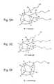
- the first coatinghas a first component comprising a silicon oxide cage complex and a second component comprising one or more nanostructure binding moieties.
- Exemplary nanostructure binding moietiesinclude either the protonated or deprotonated forms of phosphonate, phosphinate, carboxylate, sulfonate, sulfinate, amine, alcohol, amide, and/or thiol moieties.
- Preferred nanostructure binding moietiesinclude ester moieties of phosphonate, phosphinate, carboxylate, sulfonate, and sulfinate.
- the nanostructure binding moietiesare independently coupled to the silicon oxide cage complex, e.g., via an oxygen or silicon atom of the cage.
- the coated nanostructureincludes a silsesquioxane composition as the first coating.
- the silsesquioxanecan be either a closed cage structure or a partially open cage structure.
- the silicon oxide cage complexe.g., the silsesquioxane
- the silicon oxide cage complexis derivatized with one or more boron, methyl, ethyl, branched or straight chain alkanes or alkenes with 3 to 22 (or more) carbon atoms, isopropyl, isobutyl, phenyl, cyclopentyl, cyclohexyl, cycloheptyl, isooctyl, norbornyl, and/or trimethylsilyl groups, electron withdrawing groups, electron donating groups, or a combination thereof.
- discrete silicatesare employed in the first coating composition.
- One discrete silicate which can be used as first coatingsis phosphosilicate.
- the silicon oxide cage complex first coatingis typically converted to a second rigid coating comprising a silicon oxide (e.g., SiO 2 ).
- the coatings employed in the compositions of the present inventiontypically exhibit a first property in their initial (i.e., pre-conversion or pre-cured) state, and a second, differing property in the second, post-conversion or post-curing state.
- the first electrical propertycould include conductivity while the second electric property is nonconductivity (or vice versa).
- the material in the first statemay be an electron conductor or a neutral material, while the material in the second state may be a hole conductor.
- the first and second optical propertiescould be opacity and transparency, e.g. to visible light.
- the first optical propertycould include light absorption (or transmission or emission) at a first wavelength
- the second optical propertycomprises light absorption (or transmission or emission) at a second wavelength
- the material in the first statecould be a flexible molecule
- the second statecould comprise a rigid (porous or solid) shell.
- the first physical propertycomprises solubility, e.g., in a selected solvent
- the second electrical propertycomprises nonconductivity. Conversion of the coating can be accomplished, e.g., by application of heat and/or radiation.
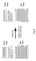
- the present inventionalso provides an array comprising a plurality of discrete coated nanostructures.
- the member nanostructuresare present at a density greater than about 1 ⁇ 10 10 /cm 2 , greater than about 1 ⁇ 10 11 /cm 2 , and more preferably at greater than about 1 ⁇ 10 12 /cm 2 or even greater than about 1 ⁇ 10 13 /cm 2 .
- the member nanostructuresare associated with a surface of a substrate, such as a silicon wafer.
- the member nanostructuresare encapsulated prior to association with the substrate surface, while in other embodiments, a first portion of a member nanostructure is associated with the substrate, and a second portion of the member nanostructure is associated with the first coating or the second coating.
- the surface of the substrateincludes a surface-binding ligand coupled to a second nanostructure binding moiety, e.g., for association with a portion of the nanostructure surface.
- a surface-binding ligandcoupled to a second nanostructure binding moiety, e.g., for association with a portion of the nanostructure surface.
- a silane moietywould function as the binding ligand on the substrate or surface.
- Devices including a plurality of discrete coated nanostructuresform another feature of the invention.
- Exemplary devices that can incorporate the discrete coated nanostructures of the inventioninclude, but are not limited to, a charge storage device, a memory device (e.g., a flash memory device), and a photovoltaic device.
- the present inventionprovides a coated nanostructure-containing composition having a plurality of nanostructures and a coating separating each member nanostructure.
- the coatingincludes a plurality of nanostructure binding moieties attached to a surface of the member nanostructure; after association of the nanostructure binding moieties with the surface of the member nanostructure, the coating can be converted to the second coating (e.g., an insulating shell; the first coating is optionally also insulating).
- the second coating or “shell”is an inflexible structure that provides a spacing (e.g., a selected or defined distance, or rigid spacing) between adjacent member nanostructures.
- the diameter of a given coated nanostructurecan range, e.g., between about 1 and about 100 nm, or optionally between about 1 nm and about 50 nm.
- a higher packing densityis desired, and thus a distance between nanostructures optionally ranges from about 1 nm to about 10 nm, about 3 nm to about 10 nm, and more preferably, between about 2 nm and about 6 nm, e.g., between about 3 and about 5 nm or about 2 nm and about 4 nm.
- the diameter of the coated nanostructurefalls within a range of from about 2 nm to about 6 nm, or optionally about 3.5 nm (or less).
- the insulating shellreduces or prevents (e.g., lateral) charge diffusion or transmission between adjacent or proximal member nanostructures, or between a nanostructure and another adjacent or proximal material or substrate.
- the shellmay reduce or prevent other types of transmission, such as light or heat.
- the insulating shellreduces the rate of charge diffusion between member nanostructures, whereby the average time for an electron to hop from one member nanostructure to another is greater than a predetermined length of time (e.g., greater than 1 millisecond, 1 second, 1 minute, 1 hour, 1 day, 1 month, or even 1 year or more).
- Nanostructure binding moietiesthat can be employed in the compositions of the present invention include, but are not limited to, one or more phosphonate ester, phosphonic acid, carboxylic acid or ester, amine, phosphine, phosphine oxide, sulfonate, sulfinate, alcohol, epoxide, amide or thiol moieties.
- the coating used to form the insulating shellcan be an organic, an inorganic, or a hybrid organic/inorganic composition.
- the nanostructure-binding coatingcomprises a silicon oxide cage complex, such as one or more silsesquioxanes or discrete silicates.
- the compositionoptionally includes a topcoat composition, e.g., one comprising the same material as the coating or the insulating shell.
- the present inventionalso provides a plurality of discrete nanostructures encompassed with rigid SiO 2 shells, wherein a diameter of a member nanostructure:shell construct (i.e., a member nanostructure with its shell) is less than about 10 nm (or optionally less than about 8 nm, less than about 6 nm, less than about 4 nm, or less than about 3.5 nm), and/or wherein the member nanostructures are present at a density greater than 1 ⁇ 10 10 /cm 2 , or optionally greater than about 1 ⁇ 10 11 /cm 2 , about 1 ⁇ 10 12 /cm 2 , or even equal to or greater than about 1 ⁇ 10 13 /cm 2 .
- a diameter of a member nanostructure:shell constructi.e., a member nanostructure with its shell
- the member nanostructuresare present at a density greater than 1 ⁇ 10 10 /cm 2 , or optionally greater than about 1 ⁇ 10 11 /cm 2 , about 1 ⁇ 10 12
- the member nanostructuresare optionally arranged in an array, e.g., an ordered or disordered array. Essentially all of the features described for the embodiments above apply to these embodiments as well, as relevant; for example, with respect to type of nanostructures, association with a substrate, inclusion in devices, topcoats, and/or the like.
- the present inventionalso provides devices, systems, compositions, films, and the like having therein a plurality of discrete coated nanostructures.
- One exemplary device that could be used with the discrete coated nanostructures of the present inventionis a memory device, e.g., a flash memory device.
- the flash memory deviceincludes a plurality of discrete nanostructures encompassed with rigid SiO 2 shells, wherein a diameter of a member nanostructure is less than about 6 nm, and wherein the member nanostructures are present at a density greater than about 1 ⁇ 10 10 /cm 2 , or more preferably, densities greater than about 1 ⁇ 10 12 /cm 2 .
- Other exemplary devicesinclude charge storage devices and photovoltaic devices.
- the present inventionprovides methods for post-deposition shell formation on a nanostructure.
- the methodsinclude the steps of providing one or more nanostructures having a ligand composition associated with a first surface, which ligand composition is capable of being converted to a rigid shell, and converting or curing the ligand composition and generating the rigid shell on the first surface of the nanostructure, thereby forming the shell after deposition of the ligand composition.
- the ligand compositioncan be, e.g., any of those described herein.
- the nanostructurescan be provided by synthesizing one or more nanowires, nanorods, nanotubes, branched nanostructures, branched nanocrystals, nanotetrapods, nanotripods, nanobipods, nanocrystals, nanodots, quantum dots, nanoparticles, or branched tetrapods (or a combination thereof) by any of a number of techniques known in the art.
- providing the one or more nanostructuresinvolves providing semiconductor nanocrystals or metal nanocrystals having at least one dimension of less than 10 nm, less than about 5 nm, or between 2-4 nm or smaller.
- the nanostructures having a ligand composition associated with a first surfaceare provided by providing one or more nanostructures having one or more surfactants associated with the first surface and exchanging the surfactants with the ligand composition.
- the step of exchanging the surfactantscan be achieved by various procedures.
- the surfactantse.g., carboxylic acids, fatty acids, phosphines and/or phosphine oxides
- the surfactantse.g., carboxylic acids, fatty acids, phosphines and/or phosphine oxides
- Organic solventsthat can be employed for this step include, but are not limited to, toluene, chloroform, chlorobenzene, and combinations thereof.
- the surfactantscan be removed in situ (e.g., after deposition on a substrate) by various techniques, such as performing a low temperature organic stripping procedure followed by oxidation using a reactive oxygen species (provided, e.g., by UV ozone generation, RF monoatomic oxygen generation, or oxygen radical generation).
- the ligand compositioncan then be associated with the stripped nanostructures.
- the nanostructuresare synthesized in the presence of the ligand composition, and thus no surfactant exchange step is required.
- the methods of the present inventioninclude the step of converting or curing the ligand composition to generate a second coating (e.g., in some embodiments, a rigid and/or insulating shell) on the first surface of the ligand-exchanged nanostructure.
- the curing stepis performed by heating the nanostructure having the ligand composition associated therewith at temperatures that will not degrade or otherwise compromise the nanostructure.
- curingis typically achieved at temperatures less than about 500° C. In some embodiments, the heating process is performed between 200-350° C.
- the curing processresults in the formation of the second coating or shell (e.g., a thin, solid matrix on the first surface of the nanostructure).
- the shellcan comprise, for example, an electrically conductive composition, an electrically insulating composition, an optically transparent composition, an optically opaque composition, or even a combination of these features.
- the second coatingis a rigid insulating shell comprising a glass or glass-like composition, such as SiO 2 .
- the curing stepis optionally performed by heating the nanostructure in an oxidizing atmosphere.
- heating the nanostructure in an oxidizing atmospherecan convert the metal to a metal oxide.
- the metal oxideis optionally converted to the metal by heating the nanostructure in a reducing atmosphere, e.g., after the nanostructure is processed (which can include, e.g., exposing the nanostructure to a temperature between about 200° C. and about 750° C., or even greater than 750° C.) and/or disposing a dielectric on the nanostructure.
- the nanostructures employed in the methods of the present inventionare coupled to a substrate, e.g., via a second nanostructure surface.
- a substratee.g., a silicon substrate (e.g., with or without a silicon oxide coating).
- Another exemplary substrateis a silicon nitride surface, either on a silicon wafer, transmission electron microscope (TEM) grid, or other suitable substrate.
- coated nanostructuresare coupled via a second nanostructure surface (e.g., a portion of the surface not in contact with the ligand composition).
- the methods of the present inventionfurther include the step of applying a planarization composition, e.g., a spin-on glass planarization composition, to the one or more nanostructures coupled to a substrate. While this optional step can be performed either prior to or after the curing step, the planarization composition is preferably applied after curing of the ligand into the rigid shell.
- a planarization compositione.g., a spin-on glass planarization composition
- the present inventionprovides nanostructures having a rigid shell formed post-deposition as prepared by the methods described herein.
- the rigid shellcomprises silicon (for example, SiO 2 ) and/or boron (e.g., B 2 O 3 ).
- the present inventionalso provides methods of reversibly modifying nanostructures.
- one or more nanostructures comprising a metalare provided.
- the metalis oxidized to produce a metal oxide, and the nanostructures are processed.
- the metal oxideis then reduced to provide the metal.
- the metalcan be oxidized by heating the nanostructures in an oxidizing atmosphere (e.g., one comprising oxygen).
- the nanostructuresare typically heated to a temperature between about 200° C. and about 700° C. (e.g., between about 200° C. and about 500° C.).
- the metal oxidecan be reduced by heating the nanostructures in a reducing atmosphere, e.g., an atmosphere comprising hydrogen, e.g., a forming gas.
- nanostructurerefers to a structure having at least one region or characteristic dimension having a dimension of less than about 500 nm, e.g., less than about 100 nm, less than about 50 nm, or even less than about 10 nm or about 5 nm. Typically, the region or characteristic dimension will be along the smallest axis of the structure. Examples of such structures include nanowires, nanorods, nanotubes, branched nanocrystals, nanotetrapods, tripods, bipods, nanocrystals, nanodots, quantum dots, nanoparticles, branched tetrapods (e.g., inorganic dendrimers), and the like.
- Nanostructurescan be substantially homogeneous in material properties, or in certain embodiments can be heterogeneous (e.g., heterostructures). Nanostructures can be, e.g., substantially crystalline, substantially monocrystalline, polycrystalline, metallic, polymeric, amorphous, or a combination thereof. The nanostructures can comprise, e.g., a metal, semiconductor, insulator, or a combination thereof. In one aspect, each of the three dimensions of the nanostructure has a dimension of less than about 500 nm, e.g., less than about 200 nm, less than about 100 nm, less than about 50 nm, less than about 10 nm, or even less than about 5 nm.
- crystallineor “substantially crystalline,” when used with respect to nanostructures, refer to the fact that the nanostructures typically exhibit long-range ordering across one or more dimensions of the structure. It will be understood by one of skill in the art that the term “long range ordering” will depend on the absolute size of the specific nanostructures, as ordering for a single crystal cannot extend beyond the boundaries of the crystal. In this case, “long-range ordering” will mean substantial order across at least the majority of the dimension of the nanostructure.
- a nanostructurecan bear an oxide or other coating, or can be comprised of a core and at least one shell. In such instances it will be appreciated that the oxide, shell(s), or other coating need not exhibit such ordering (e.g.
- crystallinerefers to the central core of the nanostructure (excluding the coating layers or shells).
- crystallineor “substantially crystalline” as used herein are intended to also encompass structures comprising various defects, stacking faults, atomic substitutions, and the like, as long as the structure exhibits substantial long range ordering (e.g., order over at least about 80% of the length of at least one axis of the nanostructure or its core).
- the interface between a core and the outside of a nanostructure or between a core and an adjacent shell or between a shell and a second adjacent shellmay contain non-crystalline regions and may even be amorphous. This does not prevent the nanostructure from being crystalline or substantially crystalline as defined herein.
- nanocrystallinewhen used with respect to a nanostructure indicates that the nanostructure is substantially crystalline and comprises substantially a single crystal.
- a nanostructure heterostructurecomprising a core and one or more shells
- monocrystallineindicates that the core is substantially crystalline and comprises substantially a single crystal.
- a “nanocrystal”is a nanostructure that is substantially monocrystalline.
- a nanocrystalthus has at least one region or characteristic dimension with a dimension of less than about 500 nm, e.g., less than about 200 nm, less than about 100 nm, less than about 50 nm, or even less than about 20 nm.
- the term “nanocrystal”is intended to encompass substantially monocrystalline nanostructures comprising various defects, stacking faults, atomic substitutions, and the like, as well as substantially monocrystalline nanostructures without such defects, faults, or substitutions.
- the core of the nanocrystalis typically substantially monocrystalline, but the shell(s) need not be.
- each of the three dimensions of the nanocrystalhas a dimension of less than about 500 nm, e.g., less than about 200 nm, less than about 100 nm, less than about 50 nm, or even less than about 20 nm.
- nanocrystalsinclude, but are not limited to, substantially spherical nanocrystals, branched nanocrystals, and substantially monocrystalline nanowires, nanorods, nanodots, quantum dots, nanotetrapods, tripods, bipods, and branched tetrapods (e.g., inorganic dendrimers).
- a “substantially spherical nanocrystal”is a nanocrystal with an aspect ratio between about 0.8 and about 1.2.
- Nanorodis a nanostructure that has one principle axis that is longer than the other two principle axes. Consequently, the nanorod has an aspect ratio greater than one. Nanorods of this invention typically have an aspect ratio between about 1.5 and about 10, but can have an aspect ratio greater than about 10, greater than about 20, greater than about 50, or greater than about 100, or even greater than about 10,000. Longer nanorods (e.g., those with an aspect ratio greater than about 10) are sometimes referred to as nanowires.
- the diameter of a nanorodis typically less than about 500 nm, preferably less than about 200 nm, more preferably less than about 150 nm, and most preferably less than about 100 nm, about 50 nm, or about 25 nm, or even less than about 10 nm or about 5 nm.
- Nanorodscan have a variable diameter or can have a substantially uniform diameter, that is, a diameter that shows a variance less than about 20% (e.g., less than about 10%, less than about 5%, or less than about 1%) over the region of greatest variability.
- Nanorodsare typically substantially crystalline and/or substantially monocrystalline, but can be, e.g., polycrystalline or amorphous.
- a “branched nanostructure”is a nanostructure having three or more arms, where each arm has the characteristics of a nanorod, or a nanostructure having two or more arms, each arm having the characteristics of a nanorod and emanating from a central region that has a crystal structure distinct from that of the arms. Examples include, but are not limited to, nanobipods (bipods), nanotripods (tripods), and nanotetrapods (tetrapods), which have two, three, or four arms, respectively.
- a “nanotetrapod”is a generally tetrahedral branched nanostructure having four arms emanating from a central region or core, where the angle between any two arms is approximately 109.5 degrees.
- the corehas one crystal structure and the arms have another crystal structure.
- Nanoparticleis any nanostructure having an aspect ratio less than about 1.5.
- Nanoparticlescan be of any shape, and include, for example, nanocrystals, substantially spherical particles (having an aspect ratio of about 0.9 to about 1.2), and irregularly shaped particles.
- Nanoparticlescan be amorphous, crystalline, partially crystalline, polycrystalline, or otherwise.
- Nanoparticlescan be substantially homogeneous in material properties, or in certain embodiments can be heterogeneous (e.g. heterostructures).
- the nanoparticlescan be fabricated from essentially any convenient material or materials.
- An “aspect ratio”is the length of a first axis of a nanostructure divided by the average of the lengths of the second and third axes of the nanostructure, where the second and third axes are the two axes whose lengths are most nearly equal each other.
- the aspect ratio for a perfect rodwould be the length of its long axis divided by the diameter of a cross-section perpendicular to (normal to) the long axis.
- the “diameter” of a nanostructurerefers to the diameter of a cross-section normal to a first axis of the nanostructure, where the first axis has the greatest difference in length with respect to the second and third axes (the second and third axes are the two axes whose lengths most nearly equal each other).
- the first axisis not necessarily the longest axis of the nanostructure; e.g., for a disk-shaped nanostructure, the cross-section would be a substantially circular cross-section normal to the short longitudinal axis of the disk. Where the cross-section is not circular, the diameter is the average of the major and minor axes of that cross-section.
- a diameteris typically measured across a cross-section perpendicular to the longest axis of the nanowire or nanorod.
- the diameteris measured from one side to the other through the center of the sphere.
- the term “coating”refers to a ligand that has been applied to a surface, such as the surface of a nanostructure.
- the coatingeither can fully or partially encapsulate the structure to which it has been applied.
- the coatingcan be porous or solid.
- optical propertyrefers to physical characteristics involving the transmission or generation of photons.
- the term “electrical property”refers to refers to physical characteristics involving the transmission or generation of electrons (or holes).
- high density packingor “high density” refer to densities of about 10 12 nanostructures per cm 2 or greater.
- An “organic group”is a chemical group that includes at least one carbon-hydrogen bond.
- hydrocarbon groupis a chemical group consisting of carbon and hydrogen atoms.
- alkyl grouprefers to a linear, branched, or cyclic saturated hydrocarbon moiety and includes all positional isomers, e.g., methyl, ethyl, propyl, 1-methylethyl, butyl, 1-methylpropyl, 2-methylpropyl, 1,1-dimethylethyl, pentyl, 1-methylbutyl, 2-methylbutyl, 3-methylbutyl, 2,2-dimethylpropyl, 1-ethylpropyl, hexyl, 1,1-dimethylpropyl, 1,2-dimethylpropyl, 1-methylpentyl, 2-methylpentyl, 3-methylpentyl, 4-methylpentyl, 1,1-dimethylbutyl, 1,2-dimethylbutyl, 1,3-dimethylbutyl, 2,2-dimethylbutyl, 2,3-dimethylbutyl, 3,3-dimethylbutyl, 1-ethylbutyl, 2-ethyl, 2-
- alkenyl grouprefers to a linear, branched, or cyclic unsaturated hydrocarbon moiety that comprises one or more carbon-carbon double bonds.
- alkenyl groupsinclude ethenyl, 2-propenyl, 2-butenyl, 3-butenyl, 1-methyl-2-propenyl, 2-methyl-2-propenyl, 2-pentenyl, 3-pentenyl, 4-pentenyl, 1-methyl-2-butenyl, 2-methyl-2-butenyl, 3-methyl-2-butenyl, 1-methyl-3-butenyl, 2-methyl-3-butenyl, 3-methyl-3-butenyl, 1,1-dimethyl-2-propenyl, 1,2-dimethyl-2-propenyl, 1-ethyl-2-propenyl, 2-hexenyl, 3-hexenyl, 4-hexenyl, 5-hexenyl, 1-methyl-2-pentenyl, 2-methyl-2-pentenyl, 3-methyl-2-pentenyl
- alkynyl grouprefers to a linear, branched, or cyclic unsaturated hydrocarbon moiety that comprises one or more carbon-carbon triple bonds.
- Representative alkynyl groupsinclude, e.g., 2-propynyl, 2-butynyl, 3-butynyl, 1-methyl-2-propynyl, 2-pentynyl, 3-pentynyl, 4-pentynyl, 1-methyl-2-butynyl, 1-methyl-3-butynyl, 2-methyl-3-butynyl, 1,1-dimethyl-2-propynyl, 1-ethyl-2-propynyl, 2-hexynyl, 3-hexynyl, 4-hexynyl, 5-hexynyl, 1-methyl-2-pentynyl, 1-methyl-3-pentynyl, 1-methyl-4-pentynyl, 2-methyl-3-pentynyl, 2-methyl-4-pentynyl
- aryl grouprefers to a chemical substituent comprising or consisting of an aromatic group.
- exemplary aryl groupsinclude, e.g., phenyl groups, benzyl groups, tolyl groups, xylyl groups, alkyl-aryl groups, or the like.
- Aryl groupsoptionally include multiple aromatic rings (e.g., diphenyl groups, etc.).
- the aryl groupcan be, e.g., substituted or unsubstituted. In a “substituted aryl group”, at least one hydrogen is replaced with one or more other atoms.
- alkyl-aryl grouprefers to a group that comprises alkyl and aryl moieties.
- heteroatomrefers to any atom which is not a carbon or hydrogen atom. Examples include, but are not limited to, oxygen, nitrogen, sulfur, phosphorus, and boron.
- a “surfactant”is a molecule capable of interacting (whether weakly or strongly) with one or more surfaces of a nanostructure.
- FIG. 1depicts exemplary silsesquioxane frameworks for use as nanostructure ligands in the present invention.
- FIG. 2provides an exemplary discrete silicate ligand having a phosphate moiety incorporated as a nanostructure binding head group.
- FIG. 3provides a schematic depiction of the preparation of a substrate using ligand-coated quantum dots.
- surfactantscrystal synthesis ligands
- a phosphosilicate ligandIn the middle panel, an SiO 2 surface is coated with a silane ligand to form a self assembled monolayer of surface assembly ligand (SAL).
- SALsurface assembly ligand
- the ligand exchanged nanodotsare applied to the SAL coated substrate, leaving a close-packed monolayer of CdSe dots on the SiO 2 substrate with SiO 2 between the dots after assembly, washing, and curing steps.
- FIG. 4provides a schematic side-view (top) and top-view (bottom) depiction of the conversion of a first coating to a second coating on a plurality of adjacent quantum dots.
- the views on the leftshow a close-packed monolayer of CdSe dots on an SiO 2 substrate with an SiO 2 ligand between the dots.
- the views on the rightshow a close-packed monolayer of CdSe dots on the SiO 2 substrate with SiO 2 between the dots.
- FIG. 5provides exemplary first coating compositions of the present invention.
- FIG. 6provides an exemplary synthesis protocol for the production of the silsesquioxane ligand heptacyclopentyl POSS disilanol diethoxyphosphate.
- Nanostructures having improved energy barrier heights and/or quantum confinementcould be used, e.g., for quantized charge storage and/or transfer in the field of microelectronics, or for photon generation and transfer in photonics.
- solid state storage devicessuch as flash memory devices use storage media having discrete read and write properties.
- Enhanced storage capacitiescould be implemented by storing charge on densely-packed discrete nanostructures, such as quantum dots.
- nanostructures that pack well at high densitye.g., those having spherical, nearly spherical, and/or isotropic structures, such as nanodots or quantum dots
- improved quantum confinement propertiesare particularly promising for use in discrete and/or quantized charge storage, as well as for photon generation and transfer.
- compositions, methods and devicesin which nanostructured charge storage elements are able to be closely packed (e.g. at densities of 1 ⁇ 10 10 /cm 2 or greater, even at a high density, e.g., at 1 ⁇ 10 12 /cm 2 or greater), while preserving or improving quantum confinement, either by controlling the distance between the nanostructures and/or by introducing an insulating or dielectric coating material such as silicon dioxide around discrete nanostructures.
- the nanostructuresare preferably provided as one or more close-packed ordered monolayers.
- hexagonally packed monolayers of CdSehave been prepared in the art by making use of phase segregation between aliphatic surfactants on the nanocrystals and aromatic conjugated organic materials, and deposition via spin-coating.
- the embedding of nanocrystals into (or on top of) an organic matrixis not desirable in memory device fabrication processes.
- the present inventionprovides, in one embodiment, monolayers of quantum dots with silsesquioxane or silicate ligand surface ligands prepared by various self-assembly methods and compatible with charge storage applications.
- Maintaining a selected distance between nanostructurescan be achieved using a ligand or coating associated with the nanostructure surface.
- the size of the ligand-nanostructure complex, and thus the distance between adjacent nanostructures,can be varied for different applications by altering the composition of the associated ligand.
- the size of the ligandcan be used to control dot-to-dot spacing during the preparation of a nanostructure-containing substrate or matrix.
- the physical properties of the nanostructure compositioncan also be adjusted by introducing a ligand coating that can be converted to a second coating having a second, desired property (for example, being dielectric).
- a ligand coatingthat can be converted to a second coating having a second, desired property (for example, being dielectric).
- the coated nanocrystals in their “post-processing” or cured stateare insulated with silicon dioxide-containing second coatings or shells, e.g., to reduce cross-talk between nanocrystals.
- Other desirable propertiesinclude, but are not limited to, malleability, rigidity, thermal tolerance, conductivity, transparency, and opaqueness (opacity), depending upon the application involved.
- ligand compositions that, upon conversion to a second coating, affect the HOMO or valence bond levels of the nanostructure compositionare also included in the compositions of the present invention.
- the present inventionand or various individual or combined component aspects thereof, possess far broader applicability than that which is embodied by these specific applications.
- the ability to provide or include a convertible coating that can be converted in situ, or otherwise when desiredhas broadly applicable value.
- optical coatingsmay be deposited using a coating material that offers a first optical property, but which may be converted to a second optical property, post-deposition.
- the ability to individually associate a coating with a nanostructure, which coating may be more easily manipulated in one form, but may be later converted while already uniformly or otherwise desirably coated onto the nanostructureprovides significant advantages to previously described nanostructure coating processes.
- the present inventionprovides methods and compositions involving discrete coated nanostructures. These nanostructures differ from nanostructures embedded in a matrix, in that each coated nanostructure has, upon synthesis or after subsequent application, a defined boundary provided by the coating that is not contiguous with the surrounding matrix.
- the coating materialis generally referred to herein as a “ligand” in that such coating typically comprises molecules that have individual interactions with the surface of the nanostructure, e.g., covalent, ionic, van der Waals, or other specific molecular interactions.
- the present inventionalso provides a plurality of discrete coated nanostructures, in which the first coatings have been converted to the second coatings such that the individual nanostructures are not in direct contact or otherwise in undesirable communication, e.g., electrical communication.
- the second coating (shell) component of the coated nanostructureis often non-crystalline, unlike the typical core:shell type nanostructures known in the art.
- the diameters of the coated nanostructuresare less than about 10 nm, and optionally less than about 5 nm, less than about 4 nm, or even less than about 3.5 nm.
- a discrete coated nanostructure of the present inventionincludes an individual nanostructure having a first surface and a first coating associated with the first surface of the individual nanostructure and having a first optical, electrical, physical or structural property, wherein the first coating is capable of being converted to a second coating having a different electrical, optical, structural and/or other physical property than the first coating.
- the first coatingencapsulates the nanostructure (i.e., it completely surrounds the nanostructure being coated).
- the nanostructureis partially encapsulated.
- the first coatingcan cover the portion of the nanostructure not associated with another composition, such as the surface of a substrate.
- the present inventionalso provides a coated nanostructure-containing composition having a plurality of nanostructures having a first coating separating each member nanostructure.
- the coatinghas a plurality of nanostructure binding moieties that are employed to attach the coating to the surface of the member nanostructures.
- the first coatingthen can be converted to a second coating or shell that possesses at least one different property from the original coating, e.g., a coating that is electrically, optically, chemically, and/or structurally different, e.g., insulative as opposed to conductive (or at least non-insulative), or rigid instead of malleable.
- An insulating coating (or insulating shell) as described hereincomprises a material that is nonconductive (e.g., dielectric).
- An insulating shellis generally capable of preventing substantial charge transfer for at least a brief length of time; for example, the insulating shell can reduce the rate of charge diffusion between member nanostructures, such that the average time for an electron to hop from one member nanostructure to another is at least a millisecond, or optionally at least 10 milliseconds, at least 100 milliseconds, at least 1 second, at least 1 minute, at least 1 hour, at least 1 day, at least 1 month, or at least 1 year or longer.
- the charge transferis substantially prevented (e.g., a device comprising the insulated nanostructures can maintain an applied charge) for a predetermined length of time ranging from 1 millisecond to at least 1 second, 1 minute, 1 hour, 1 day, 1 year, or longer.
- a convertible coating mechanism in accordance with the present inventione.g., as opposed to a synthesized nanocrystal that includes a shell component, one can garner a number of advantages, including, e.g., providing smaller core-shell structures, and potentially more coherent shell layers, that allow higher packing densities when such nanocrystals are arranged in a layer, e.g., a monolayer.
- a layere.g., a monolayer.
- providing the plurality of nanostructures at a density of about 1 ⁇ 10 10 /cm 2is sufficient.
- the plurality of nanostructures in the nanostructure-containing composition layerare present at a density of about 1 ⁇ 10 11 /cm 2 or greater, or about 1 ⁇ 10 12 /cm 2 or greater, and more preferably, at about 1 ⁇ 10 13 /cm 2 or greater.
- the plurality of discrete coated nanostructuresare provided as a monolayer.
- the plurality of nanostructuresincludes multiple monolayers, each independently having a selected or desired density of member nanostructures.
- the plurality of coated nanostructuresfunction as charge storage elements in various high-density data storage applications.
- Two key requirements for the use of the plurality of coated nanostructures in these applicationsare the selection of appropriate surface properties, and close packing of the nanostructures in monolayer arrays, optionally well-ordered monolayer arrays. As shown by Bulovic and coworkers (Coe et al.
- the organic layer(s)are not compatible with typical memory fabrication techniques.
- coated nanostructureswhich are more compatible with charge storage applications are provided by the present invention.
- the plurality of coated nanostructures of the present inventioncomprise one or more monolayers of nanodots having silsesquioxane or silicate ligand surface ligands. These can be prepared, for example, by various self-assembly methods as described herein; after curing, the resulting nanostructures are insulated by the second coating of silicon dioxide-containing ligands.
- the oxide second coatingreduces cross-talk between nanostructures.
- the ligands employed as first coatings in the compositions, devices and methods of the present inventionare prepared as a means by which to generate a second coating having a selected or desired property (or properties).
- the second coatingprovides an altered electrical, optical, physical or structural state as compared to the first coating, such as changes in rigidity, solubility, and/or in optical properties (refractive index, emission and/or absorption properties).
- a variety of coating compositionsare considered for use in the present invention.
- the coatingcan be an organic composition, such as various polymeric precursors that may be chemically or radiatively converted to altered (second) coating compositions, e.g., through cross-linking, further polymerization, etc.
- Exemplary organic compositionsinclude, but are not limited to, dendrimer PAMAM (amine dendrimer), amine-(or other nanocrystal binding head group) terminated methyl methacrylate (polymethylmethacrylate precursor), phosphonate head group-containing polymers, carboxylic acid-terminated diene or diacetylene compositions, any heteroatom containing monomer(s) that can be converted to polymers upon chemical, heat or light activation, as well as the ligands described in by Whiteford et al. in U.S. Ser. No. 10/656,910 filed Sep. 4, 2003, and titled “Organic Species that Facilitate Charge Transfer to/from Nanostructures.”
- the coatingis an inorganic composition.
- the coatingincludes a silicon or silicon oxide moiety.
- silicon oxidecan be understood to refer to silicon at any level of oxidation.
- silicon oxidecan refer to the chemical structure SiO x , wherein x is between 1 and 2 inclusive.
- Inorganic coatings for use in the present inventioninclude, but are not limited to, tin oxide, vanadium oxide, manganese oxide, titanium oxide, zirconium oxide, tungsten oxide, and niobium oxide, silicon carbide, silicon nitride, as well as other silicon-containing coatings and/or boron-containing coatings.
- the coatingcomprises a hybrid organic/inorganic composition, such as some embodiments of the silicon oxide cage complexes provided herein. See also the compositions provided in Schubert (2001) “Polymers Reinforced by Covalently Bonded Inorganic Clusters” Chem. Mater. 13:3487-3494; Feher and Walzer (1991) “Synthesis and characterization of vanadium-containing silsesquioxanes” Inorg. Chem. 30:1689-1694; Coronado and Gomez-Garc ⁇ a (1998) “Polyoxometalate-Based Molecular Materials” Chem. Rev. 98:273-296; Katsoulis (1998) “A Survey of Applications of Polyoxometalates” Chem. Rev.
- the coatingis a silicon-containing coating (e.g., either an inorganic or hybrid inorganic/organic composition) that can be converted to a rigid SiO 2 insulating shell after deposition of the coating and association of the nanostructure binding moieties with the surface of the member nanostructure.
- the present inventionprovides coated nanostructures in which the second coating comprises a rigid SiO 2 shell, and wherein a diameter of the discrete coated nanostructure is optionally less than or equal to 50 nm, less than or equal to 20 nm, less than or equal to 10 nm, less than or equal to 6 nm, or less than or equal to 3.5 nm.
- the coatingcan be used to provide spacing between adjacent member nanostructures, e.g., during preparation of substrate-bound nanostructure compositions (see, for example, the embodiment depicted in FIGS. 3 and 4 ).
- the coating ligands of the present inventionare sized such that the coated nanostructures can be packed to provide less than about 10 nm between nanostructures (center to center), or optionally less than about 8 nm, less than about 5 nm, or less than about 4 nm between nanostructure centers.
- the coatingprovides a spacing of between about 8-10 nm, about 4-8 nm, or preferably about 2-4 nm between nanostructure surfaces (e.g., the ligands are 1-2 nm in length).
- the coating composition or the rigid shellreduces or prevents charge diffusion between member nanostructures.
- Coating compositions that can be converted into second coatings of oxides of silicon and/or boronare particularly preferred in this embodiment.
- the coated nanostructuresare associated with a substrate and/or overlaid with a topcoat material.
- the top coating materialis a similar composition to that of either the first coating or second coating.
- a plurality of the nanostructurescan be overlaid with a composition that can also be converted to SiO 2 , thus embedding the nanostructures in a matrix of silicon.
- the ligands employed as first coatings in the compositions, devices and methods of the present inventionare prepared as a means by which to generate a second coating having a selected or desired property (or properties).
- a second coatinghaving a selected or desired property (or properties).
- quantum dots used in flash memory devicesneed to maintain discrete boundaries between adjacent nanostructures. This can be achieved by providing a ligand that can be converted to a rigid shell (second coating) having a defined diameter, thus controlling the distance between dots.
- device performancecan be improved if the second coating also functions to improve quantum confinement and reduce cross-talk between quantum dots; a ligand that produces a second coating that has dielectric characteristics is also desirable.
- the present inventionprovides ligand compositions for use as first coatings, for use in the generation of discrete coated nanostructures having e.g., improved barrier heights and/or quantum confinement.
- the first coating and second coatingtypically have differing physical properties.
- the first coatingcan be electrically neutral (the first electrical property) while the second coating comprises a dipole moment (the second electrical property); similarly, the first coating can comprise a dipole moment while the second coating is electrically neutral.
- the first coatingis non-insulating or conductive (e.g., a conjugated conducting organic-metal hybrid species), while the second coating is insulating or nonconductive (e.g., a metal oxide).
- the first coatingis insulating or nonconductive
- the second coatingis non-insulating or conductive.
- malleable first coatingsthat are converted to rigid second coatings (particularly those having semiconductive or insulating properties).
- One preferred composition embodiment for use as a rigid insulating shell encapsulating the selected nanostructureis silicon oxide (SiO 2 ); such rigid SiO 2 second coatings are optionally produced from malleable first coatings comprising silicon oxide caged complexes (e.g., silsesquioxanes).
- the first and second coatingsmay differ in optical properties.
- the first optical propertycomprises light absorption or emission at a first wavelength
- the second optical propertycomprises light absorption or emission at a second wavelength (e.g., by a lanthanide-containing coating or the like).
- the first optical propertycould be reduced or non-transmission of light (opaqueness) while the second optical property is transparency (or vice versa).
- Another embodiment of interestincludes first and second coatings that have different bandgap energies, e.g., to alter the electron and/or conductivity properties of the coated nanostructure.
- the first and second coatingscan differ in a physical property such as solubility, e.g., in a selected solvent.
- the first coatingcan render the coated nanostructures soluble in a selected solvent, to facilitate dispersal, deposition, or the like of the nanostructures, while nanostructures including the second coating are less soluble in the selected solvent.
- the first and second coatingscan have combinations of the above properties; for example, the first coating may increase solubility in a selected solvent, while the second coating is nonconductive.
- the ligand coating used to coat the nanostructuresis a silicon oxide cage complex.
- the polycyclic silicon-containing compounds known as silsesquioxanese.g., polyhedral oligomeric silsesquioxanes (POSS)
- PHSQhydrogen silsesquioxane
- MSQmethyl silsesquioxane
- additional silsesquioxane structuresare provided in FIG.
- R groupsinclude a variety of chemical moieties, including, but not limited to, short chain alkyl groups such as methyl, ethyl, isopropyl, isobutyl, longer chain alkyl groups such as isooctyl and norbornyl, as well as aromatic and non-aromatic cyclic structures such as phenyl, cyclopentyl, cyclohexyl and cycloheptyl groups.
- the silsesquioxanecan be either a closed cage structure or a partially open cage structure (e.g., in which some of the ring oxygens are not coupled to both adjacent silicon atoms; see for example, FIG. 5B ).
- the non-silicate organic groupwhich is located along an edge or at a corner of the cage complex, can be functionalized to accommodate binding of the ligand to an exposed surface of the nanostructure.
- the non-silicate groupcan function as an electron withdrawing (or electron donating) group.
- Functional groups which can be incorporated into the silsesquioxane moietyinclude, but are not limited to, alkyl, alcohol, phosphine, phosphonate, thiol, ether, carboxylate, amine, epoxide, alkene and aryl groups, as well as other nanostructure binding moieties, solubilizing moieties, or electron withdrawing/donating groups of interest.
- One preferred derivatizationis the incorporation of boron into the silicon oxide cage monomer, which, will produce a second coating of boron oxide and silicon oxide upon heat treatment.
- silsesquioxane frameworksare provided in FIG. 1 .
- Silsesquioxanescan be either purchased or synthesized, for example, by hydrolytic condensation of RSiCl 3 or RSi(OR) 3 monomers (see, for example, Feher et al. (1989) J. Am. Chem. Soc. 111:1741; Brown et al. (1964) J. Am. Chem. Soc. 86:1120; Brown et al. (1965) J. Am. Chem. Soc. 87:4313-4323).
- caged structures formed during synthesiscan be directed by manipulation of the reaction conditions including solvent choice, pH, temperature, and by the choice of R-group substituent (Feher et al. (1995) Polyhedron 14:3239-3253).
- Additional silsesquioxane frameworkse.g., for derivatization with nanostructure binding moieties are available from Hybrid Plastics (Fountain Valley, Calif.; on the world wide web at hybridplastics.com).
- the silsesquioxane frameworksare coupled to one or more nanostructure binding moieties prior to use as compositions or in the methods of the present invention.
- Any of a number of standard coupling reactions known in the artcan be used to derivatize the silsesquioxane framework, e.g. with one or more nanostructure binding head groups. See, for example, the reactions described in Feher et al. (1995) Polyhedron 14:3239-3253.
- Silsesquioxane compositions for use as first coatings in the present inventioninclude (but are not limited to) the compositions provided in FIG. 5 and Table 1.
- Additional discrete silicatescan also be derivatized with nanostructure binding moieties to form compositions of the present invention.
- cyclopentyltrimethoxysilaneCAS 143487-47-2
- the nanostructure binding head groupcan then be coupled to one or more of the free hydroxyl positions, either before or after cage formation.
- Phosphosilicate ligandsare another preferred embodiment for use in the compositions and methods described herein. As depicted in FIG. 2 , the phosphate group on the phosphosilicate ligand can be utilized to couple the ligand to a nanostructure. Preferably, phosphosilicate ligands that could be thermally decomposed into SiO 2 are utilized in the methods and compositions of the present invention; shells incorporating SiO 2 would lead to higher barrier height than ZnS, and potentially higher temperature tolerances during subsequent processing or manufacturing steps. Exemplary phosphosilicate ligands are provided in FIG. 5 , panels A and B.
- FIG. 5Additional ligands having thiol moieties as the nanostructure binding head groups are depicted in FIG. 5 , panels D-I. It will be evident that certain nanostructure binding groups are preferred for certain nanostructure compositions; for example, ligands having thiol (e.g., aryl thiol) moieties are preferred ligands for certain metal nanostructures (e.g., Pd nanostructures).
- thiole.g., aryl thiol
- metal nanostructurese.g., Pd nanostructures
- Exemplary nanostructure binding moietiesinclude, but are not limited to: the protonated or deprotonated forms of phosphonate, phosphinate, carboxylate, sulfonate, sulfinate, amine, alcohol, amide, and/or thiol moieties, ester moieties of phosphonate, phosphinate, carboxylate, sulfonate, and sulfinate, phosphines, phosphine oxides, and epoxides.
- the ligand coating used to coat the nanostructuresis a polyoxometalate.
- Polyoxometalatesare metal-oxygen cluster anions, typically formed from early transition metals (V, N, Ta, Mo and W) in their highest oxidation state. Numerous derivatives can be prepared from polyoxometalate compositions, including halide, alkoxyl, thiol, phospho, and organosilyl derivatives; for a good review, see Gouzerh and Proust (1990) Chem. Rev. 98:77-111.
- polyoxovandanate derivativescan be used as first coatings in the compositions and methods of the present invention. The first ligands would then be converted to a second coating comprising vanadium oxide, having properties comparable to those of silicon oxides.
- the polyoxometalatescan be used as a first coating on the nanostructure, and subsequently converted to a second coating having differing properties.
- Certain polyoxometalatesfor example, acid forms of molybdenum and tungsten-based polyoxometalates
- have photochromic or electrochromic propertieswhich can be reduced or altered upon conversion to a second coating (e.g., by treatment with an organic reducing agent, or by exposure to an externally applied electric field (see, for example, Yamase (1998) Chem. Rev. 98:307-325)).
- the second ligandincludes a catechol functional group, which can be used to tune the electrochemical properties of the second coating.
- Catechol functional groups for use in the present inventioninclude, but are not limited to, pyrocatechol, salicylic acid, and 2,2-biphenol (see, for example, Gigant et al. (2001) J. Am. Chem. Soc. 123:11632-11637).
- the second coatingis an insulating composition (e.g., used to form an insulating shell around the nanostructure).
- the second coatingis a metal oxide, or a glass or glass-like composition capable of forming oxide polyhedra.
- Silicon dioxide (SiO 2 ), boron oxide (B 2 O 3 ), and titanium oxide (TiO 2 )are preferred second coatings components that can be generated from the first coatings of the present invention by, e.g., thermal degradation (although other oxidation states can also be employed).
- second coatings of interestinclude, but are not limited to, compositions including GeO 2 , P 2 O 5 , AsO 5 , P 2 O 3 , As 2 O 3 , Sb 2 O 3 , V 2 O 5 , Nb 2 O 5 , Ta 2 O 5 , SnO 2 and WO 3 , as well as other oxidation states of the provided metal oxides.
- compositions for use as the first coating in the present inventionare provided in Table 1 below, as well as in FIGS. 5 and 6 .
- TABLE 1Compound 1 where R is a cyclopentyl group
- Compound 2where R is a cyclopentyl group
- Compound 3where R is a hydrogen or alkyl group
- Compound 4where R is an alkyl group, a heteroatom, or an electron withdrawing group
- Compound 5where R is an alkyl group or a nanostructure binding group
- Compound 6where R is a hydrogen, an alkyl group, or a nanostructure binding group
- Compound 7where R is a halide, a leaving group, or a nanostructure binding group
- Compound 8wherein R is an isobutyl group
- Compound 9where R is an isobutyl group
- Compound 10where R is an alkyl group or a hydrogen atom
- Compound 11where R is an alkyl group
- Compound 12where R is an iso
- Rcan be a hydrocarbon group.
- Ris an alkyl group (e.g., a cyclic alkyl group or a short alkyl group having fewer than 20 or even fewer than 10 carbon atoms), an aryl group, an alkylaryl group, an alkenyl group, or an alkynyl group.
- Ris an isobutyl group, a methyl group, a hexyl group, a cyclopentyl group, or a cyclohexyl group.
- the present inventionalso provides compositions for individually coating discrete nanostructures with a dielectric coating.
- the compositionincludes a first component comprising a silicon oxide cage complex and a second component comprising one or more nanostructure binding moieties, wherein each nanostructure binding moiety is independently coupled to the silicon oxide cage complex, e.g., via an oxygen or silicon atom.
- the compositions of the present inventionare converted to the dielectric coating after deposition of the composition on a surface of the nanostructure.
- Nanostructures prepared by any of a number of synthetic techniques known in the artcan be used to prepare a discrete coated nanostructure of the present invention, including both semiconductor and metallic nanostructures, for example.
- the first coatingis converted to the second coating after completion of synthesis of the nanostructure, e.g., after the nanostructures have been removed from any solvents or building materials used during the synthesis process.
- the first coatingis not difficult to displace from the nanostructure surface.
- the nanostructuresare associated with the surface of a substrate, such as a silicon wafer or a TEM grid.
- the substratehas been treated with a composition for association with the nanostructures, such as a functionalized self-assembly monolayer (SAM) ligand.
- SAMself-assembly monolayer
- Exemplary compositions for functionalizing the substrate surfaceinclude a silicon nitride coating, a silane ligand having a nanostructure binding moiety, or other chemical moiety that can provide or accept a proton for hydrogen-bonding to the coated nanostructure (e.g. amine, alcohol, phosphonate, fluorine or other non-carbon heteroatom).
- the silane ligandcan include structures having the formula [X 3 Si-spacer-binding group(s)] where X is a Cl, OR, alkyl, aryl, other hydrocarbon, heteroatom, or a combination of these groups, and where the spacer is an alkyl, aryl and/or heteroatom combination.
- the structure of the ligandcan be responsive to light activation, leading to crosslinking of ligands (e.g., to each other, or the surface of the SAL coated substrate) via inclusion of a photo-crosslinkable group.
- Exemplary surface ligands for use in the present invention(referred to generically as “SAL” in FIG. 4 ) are commercially available from Gelest Inc. (Tullytown, Pa.; on the world wide web at gelest.com).
- the individual nanostructures employed in the compositionsinclude, but are not limited to, a nanocrystal, a nanodot, a nanowire, a nanorod, a nanotube, a quantum dot, a nanoparticle, a nanotetrapod, a tripod, a bipod, a branched nanocrystal, or a branched tetrapod.
- the present inventionis not limited to either semiconductor nanostructures or metallic nanostructures; the type of nanostructure employed is determined in part by the purpose for which it is intended.
- the diameter (e.g., a first dimension) of the coated nanodot or quantum dotis less than about 10 nm, and optionally less than about 8 nm, 6 nm, 5 nm, or 4 nm.
- the nanostructure (e.g., dot) diametersranges from about 2 nm to about 4 nm.
- the diameter of the coated quantum dot or nanodotis less than or equal to about 6 nm, or optionally less than or equal to about 3.5 nm.
- Nanostructuressuch as nanocrystals, quantum dots, nanoparticles and the like, can be fabricated by a number of mechanisms known to one of skill in the art. Furthermore, their size can be controlled by any of a number of convenient methods that can be adapted to different materials, and they are optionally washed to remove excess surfactants remaining from their synthesis and/or excess ligands. See, for example, U.S. patent applications U.S. Ser. No. 10/796,832 to Scher et al. titled “Process for producing nanocrystals and nanocrystals produced thereby,” filed Mar. 10, 2004; U.S. Ser. No. 60/544,285 to Scher et al.
- the nanocrystalscan comprise inorganic materials, e.g., a semiconducting material selected from a variety of Group II-VI, Group III-V, or Group IV semiconductors, and including, e.g., a material comprising a first element selected from Group II of the periodic table and a second element selected from Group VI (e.g., ZnS, ZnO, ZnSe, ZnTe, CdS, CdSe, CdTe, HgS, HgSe, HgTe, MgS, MgSe, MgTe, CaS, CaSe, CaTe, SrS, SrSe, SrTe, BaS, BaSe, BaTe, and like materials); a material comprising a first element selected from Group III and a second element selected from Group V (e.g., GaN, GaP, Ga
- Metalssuch as Pd, Pt, Au, Ag, Ni, Fe, Sn, Zn, Ti, Ir, and Co can also be used in the synthesis of nanostructures for use in the present invention, as can metal oxides. Further details regarding nanocrystalline structures for use in the present invention can be found, for example, U.S. patent application Ser. No. 10/656,802, filed Sep. 4, 2003, titled “Nanocomposite Based Photovoltaic Devices” and incorporated herein by reference in its entirety for all purposes.
- the devices of the present inventionemploy nanostructures comprising small, roughly spherical CdSe or Pd nanocrystals, or other metal or semiconductor-based nanostructures that can be synthesized as spherical, nearly spherical, and/or isotropic nanoparticles (such as nanodots and/or quantum dots).
- the problemcould theoretically be addressed by growing a core structure (CdSe) having a first shell (ZnS) and an additional shell (SiO 2 ), however, this approach would also have the same disadvantages with respect to defect formation, solubility and spacing.
- the present inventioncircumvents these problems, either by performing a ligand exchange directly onto the selected nanostructure using a ligand that can be turned into a second coating (for example, an oxide) upon curing but will maintain the nanostructure solubility in organic solvents (e.g., for deposition purposes), or by growing the nanostructures in the presence of such a ligand.
- the present inventionprovides methods for post-deposition shell formation on a nanostructure. These methods include the steps of a) providing one or more nanostructures having a ligand composition associated with a first surface, which a ligand composition is capable of being converted to a second coating having differing electrical, optical, physical or structural properties (e.g., to a rigid shell), and b) curing the ligand composition and generating the second coating (e.g., the rigid shell) on the first surface of the nanostructure, thereby forming a shell on the nanostructure post-deposition of the ligand composition on the nanostructure.
- the methods of the present inventionare preferably performed at temperatures that do not compromise or degrade the structural and/or physical properties of the nanostructure.
- the nanostructures having the ligand composition associated therewithare provided by exchanging surface ligands.
- providing one or more nanostructures having a ligand composition associated with a first surfacecomprises providing one or more nanostructures having one or more surfactants associated with the first surface and exchanging the surfactants on the first surface with the ligand composition.
- the nanostructuresare synthesized in the presence of the ligand composition, and no ligand exchange is necessary.
- the methods of the present inventioncan be used to generate a shell or second coating on any of a number of nanostructures, including, but not limited to, a nanocrystal, a nanodot, a nanowire, a nanorod, a nanotube, a quantum dot, a nanoparticle, a nanotetrapod, a nanotripod, a nanobipod, a branched nanostructure, and the like.
- the methods of the present inventionare not limited to nanostructures prepared by a specific synthetic approach.
- organometallic solution-based syntheses of Pd, CdSe, CdTe and CdS nanocrystalstypically employ various surfactants and/or fatty acids as solubilizing agents (see, for example, U.S. patent publication 2002/0066401 to Peng et al. titled “Synthesis of colloidal nanocrystals,” U.S. patent publication 2003/173541 to Peng et al. titled “Colloidal nanocrystals with high photoluminescence quantum yields and methods of preparing the same,” Kim et al. (2003) NanoLetters 3:1289-1291, and Qu et al. (2001) NanoLetters 1:333-337, and references cited therein). Nanostructures prepared using these or other weakly-binding organic compositions can be employed in the methods of the present invention.
- the nanostructuresare provided by preparing or growing the initial structures (e.g., the core nanostructure components) in the presence of a weakly binding organic composition (the “growth ligand”).
- the growth ligandhas a weaker association with the nanostructure than the ligand used to generate the first coating (a “replacement ligand”), and thus can be readily exchanged, e.g., by mass action.
- the nanostructures employed in the methods of the present inventioncommonly have one or more organic compositions, or growth ligands, associated with the nanostructure surface (e.g., for solubilizing the nanostructure during the synthesis procedure).
- Typical growth ligandsinclude surfactants, for example, phosphines or phosphine oxides such as trioctyl phosphine (TOP), tri-n-butyl phosphine (TBP), or trioctyl phosphine oxide (TOPO) or acids such as hexadecyl phosphonic acid (HDPA) or octadecyl phosphonic acid (ODPA).
- TOPtrioctyl phosphine
- TBPtri-n-butyl phosphine
- TOPOtrioctyl phosphine oxide
- acidssuch as hexadecyl phosphonic acid (HDPA) or octadecyl phosphonic acid (ODPA
- the growth ligandsare exchanged for a ligand composition capable of being converted to a second ligand or second coating having a different electrical, optical, physical or structural property, thereby forming a ligand-exchanged nanostructure composition.
- the growth ligandsare exchanged for a ligand composition capable of being converted to a rigid insulating shell, such as an oxide.
- Exchanging the surfactants associated with the nanostructure surface with a ligand or first coating of the present inventioncan be achieved by any of a number of mechanisms known in the art.
- exchanging the surfactantsinvolves suspending or dissolving the nanostructures in an organic solvent, and combining the suspended nanostructures with the ligand composition.
- Solvents that can be used for the exchange processinclude any that are typically employed in conjunction with nanostructure synthesis and processing, such as toluene, chloroform, chlorobenzene, and the like.
- the temperature at which the exchanging step is performedwill depend upon the ligands involved and may range from room temperature to elevated temperatures equal or greater than 100° C., 200° C., 300° C. and the like.
- surface ligands comprising sulfonic acid moietiescan be exchanged without substantial heating, and optionally can be performed at room temperature.
- the nanostructuresare coupled to or associated with a substrate surface (e.g., a solid phase embodiment rather than in solution).
- the organic surfactants on the nanostructure surfacecan be removed in situ, for example, via a low temperature organic stripping process (at temperatures ⁇ 500° C., and optionally between 200-350° C.).
- the stripping processis optionally followed by oxidation using, e.g., a reactive oxygen species.
- the replacement ligande.g., the ligand of the first coating
- the ligand coated nanostructuresare induced to form monolayers due to intermolecular self-assembly forces.
- the present inventionprovides nanocrystals with silsesquioxane or silicate ligands tailored for charge storage applications.
- the nanostructuresare arranged into close packed arrays, or more preferably high density and/or ordered close-packed arrays. Controlled self-assembly of the close-packed arrays can be achieved by various wet-process methods, such as deposition of the nanostructure-first ligand composition onto self-assembled monolayers (SAMs) or otherwise functionalized substrates or oxides, or by evaporation-driven assembly.
- SAMsself-assembled monolayers
- the member components of the self-assembled monolayerassociate with both the surface of the substrate as well as the nanostructure, thus forming a bridge or linker between the two.
- Various SAM compositions for use in the present inventioninclude, but are not limited to, organosilanes, phosphonic acids, phosphines, thiols, amines, heteroatoms, and the like.
- the SAMconsists of a silane ligand with a binding head for the silsesquioxane or silicate ligand.
- the substratesare directly functionalized with binding groups suitable for binding to the nanocrystals.
- the nanostructuresare applied in a solution and deposited on the SAM or functionalized substrate by, e.g., spin-coating, dip-coating, spray-coating, or conventional printing technologies.
- the excess (unbound) nanostructuresare subsequently washed off the substrate using an organic solvent such as toluene or chloroform, resulting in a monolayer of nanocrystals coated with silicon-containing ligands.
- the monolayerscan be prepared by evaporation-driven assembly, without the need of specially treated substrates.
- the nanocrystalsare deposited on the substrate from solution by spin-coating, dip-coating, spray-coating, or conventional printing technologies. By controlling the de-wetting process of the solvent, well-ordered arrays of nanocrystals can be obtained.
- the substratecan be thermally annealed to cure the layer of first coating (and thereby form the second layer, which in some embodiments is a rigid insulating shell, on the first surface of the nanostructure).
- the technique used for the curing stepwill depend upon the type of ligand composition employed in the method.
- the curingcan be done under inert atmosphere, such as argon or nitrogen, or under oxygen, for example.
- the temperature of the curing processcan be adjusted for the surface ligands.
- curing the compositioncan involve heating the nanostructure having the ligand composition associated therewith to form the rigid shell on the nanostructure surface.
- Heatingcan be performed in one or more stages, and using various equipment such as a hot plate or quartz furnace (see Yang et al (2001) Proc. Natl. Acad. Sci. 25:339-343).
- the ligand:nanostructure complexis heated to less than about 500° C., and optionally, to between 200-350° C.
- Thermal curing of silsesquioxane ligandstypically involves heating the silsesquioxane-containing composition to temperatures of less than about 500° C., and preferably less than about 350° C., thereby transforming the cage structures into a network structure.
- the thermal curing processdecomposes the first coating into a second coating of SiO 2 .
- Conversion of the first coating to the second coating (or shell)can be monitored, for example, via thermogravimetric analysis using an FTIR spectrometer (see Yang (2001) supra, and references cited therein).
- conversion of the ligand composition from the first coating to a second coating or shell having altered electronic or optical propertiescan include irradiating the composition.
- the polymerization processis light activated, leading to crosslinkage of the first coating to form the organic shell (second coating).
- the one or more nanostructures provided in the methods of the present inventionare coupled to a substrate via a second nanostructure surface.
- this substrateis a silicon wafer.
- the member nanostructuresare encapsulated prior to association with the substrate surface, while in other embodiments, a first portion of a member nanostructure is associated with the substrate, and a second portion of the member nanostructure is associated with the first coating or the second coating.
- the surface of the silicon waferincludes a silane ligand coupled to a second nanostructure binding moiety, e.g., to facilitate association of the substrate with a portion of the nanostructure surface.
- the curing processis optionally followed by spin coating of another layer of e.g., first coating, silicate, or the like, onto the substrate-bound coated nanostructures, and thermal curing, thereby providing a top coating or overlay.
- the top layeris an insulating oxide layer.
- the methods of the present inventionoptionally further include the step of applying a planarization composition as the overlay or top coating composition applied to the substrate-coupled nanostructures.
- the optional planarization compositioncan be applied either before or after the step of curing the ligand composition.
- the planarization compositionfills any remaining narrow spaces and produces a (relatively) flat surface on the treated portion of the wafer and/or nanostructure composition.
- the top coating or planarization materialis compatible with the rigid shell of the coated nanostructure.
- the planarization compositionis a dielectric material (either similar or different in composition from the second coating composition).
- planarization materialsinclude, but are not limited to, various silicates, phosphosilicates, and siloxanes referred to as Spin On Glass (SOG).
- SOGSpin On Glass
- the ligand compositions of the present inventioncan be used as the planarization composition.
- the present inventionalso provides nanostructures having a rigid shell formed post-deposition as prepared by the methods described herein.
- the rigid shellcomprises silicon or silicon oxide, and the diameter of the nanostructure:shell composition is less than or equal to about 6 nm.
- the present inventionprovides methods for reducing charge diffusion among a plurality of nanostructures, e.g., nanodots, and particularly quantum dots.
- the methodsinclude the steps of coupling a ligand composition comprising an electron withdrawing group to a surface of a member nanodot (or quantum dot or other nanostructure), and forming a dipole on the surface of the member nanodot and increasing the electron affinity of the nanodot, thereby reducing any charge diffusion (such as lateral charge diffusion) among the nanodots.
- the nanostructures thus formedare used in the compositions and methods for post-deposition shell formation as described herein.
- the ligand compositions of the present inventionhave electron withdrawing characteristics and can be utilized as electron-withdrawing compositions in the present methods (e.g., silicon oxide cage complexes such as silsesquioxanes).
- the electron withdrawing compositionincludes a fluorine atom (for example, F, SiF, an SiF derivative, or a fluorine polymer such as polytetrafluoroethylene).
- the ligand compositionis a boron-containing composition (e.g., an aryl-boron oligomer or a boronic acid composition).
- the electron withdrawing compositionincludes a nanostructure binding group, such as a phosphonic acid moiety, phosphonate ester, or other nanostructure binding moiety such as those described herein, for coupling to the nanostructure surface.
- the first and second properties of the ligand compositions of the present inventionare photochromism-related properties (e.g., involving color changes induced in the coating by an incoming stimulus, such as light or other incident electromagnetic radiation).
- the electron withdrawing compositioncomprises a light-activated intramolecular salt, e.g., a spiropyran.
- Exemplary intramolecular salts for use in the methods and compositions of the present inventioninclude, but are not limited to, HOOCCH 2 CH(NH(CH 3 ) 2 )CH 2 CH 2 PO 3 H 2 . See also Léaustic et al. (2001) “Photochromism of cationic spiropyran-doped silica gel” New. J. Chem. 25:1297-1301 and references cited therein.
- the plurality of nanodotscomprises discrete quantized photon generation and transfer media or discrete quantized charge storage or charge transfer media.
- the present inventionalso provides one or more (e.g., a plurality of) nanodots (for example, quantum dots) or other nanostructures having reduced charge diffusion, as prepared by the methods described herein.
- the nanostructuresoptionally have a rigid shell formed post-deposition of the ligand composition, e.g., a rigid shell comprising silicon or silicon oxide.
- the nanostructurescan be of essentially any material, size, and/or shape. In one preferred class of embodiments, a diameter of the nanostructures is less than 6 nm, e.g., less than 3.5 nm.
- the present inventionalso provides methods for fabricating a nanostructure-based memory device that uses the nanocrystals to store charge.
- core/shell CdSe/ZnS semiconductorscan be deposited on/in a layer of conducting organic material.
- the thin ZnS shell generated by this methoddoes not have a high enough energy barrier to prevent leakage of the charge out of the nanocrystal. While this problem could theoretically be addressed by growing a very thick ZnS shell, this approach is synthetically impractical. After deposition of several monolayers of shell, the strain causes defect formation, and/or the nanocrystals become insoluble, thereby providing a practical limitation to feasible shell thickness.
- the problemmight also be addressed by growing a core (CdSe) shell (ZnS) and a third shell (SiO2), an approach that is synthetically feasible but has similar issues as to those listed above.
- the present inventiontakes the novel approach of performing a ligand exchange directly onto the nanostructure (for example, small, roughly spherical CdSe or Pd nanocrystals) using a ligand composition as provided herein (e.g., a modified silsesquioxane ligand).
- the nanostructurecan be grown in the presence of the ligand composition.
- the first coating of ligandcan be converted or cured into an oxide, and will maintain the nanostructure solubility in organic solvents for deposition purposes.
- the methods for fabricating a nanostructure-based memory device that uses the nanocrystals to store chargeinclude the steps of a) providing a plurality of nanostructures the members of which have associated therewith a weakly binding growth ligand; b) exchanging the growth ligand with a replacement ligand and forming a first coating on the member nanostructures; c) associating the coated member nanostructures with a surface of a substrate; and d) converting the first coating to a second coating that differs in one or more electrical, optical, physical or structural properties, thereby fabricating a nanostructure-based memory device.
- steps a and bare replaced by a single step, in which the nanostructures are synthesized in the presence of the ligand, whereby the ligand forms a first coating on the member nanostructures.
- nanoparticles having spherical, nearly spherical, and/or isotropic geometriesare most effective for close packing of the nanostructures.
- Exchanging the growth ligand or surfactant for a replacement ligand of the first coatingcan be done, for example, by mass action exchange.
- the binding constants for the weakly bound growth ligandare preferably less than those of the ligand for use in the first coating.
- nanostructure productcontains fewer organic contaminants than those prepared by methods currently available.
- length of the replacement ligandcan be tuned to control the diameter of the coated nanostructure and thus properly space the nanocrystals apart to reduce and/or prevent charge leakage, while still allowing high density packing.
- nanostructure-containing compositions of the present inventionMany electronic and optical applications can be manufactured using the nanostructure-containing compositions of the present invention. Particularly, any device that employs (or can be devised to employ) nanodot nanostructures would benefit from the compositions and methods of the present invention. For example, various electronic applications such as transistors and memory devices could be prepared using the nanostructure-containing compositions of the present invention. Light emitting applications, such as LEDs, back plane lighting for LCDs, phosphors, PVs, photodetectors, and photodiodes could also employ the nanostructure-containing compositions of the present invention, as could other optoelectronic devices such as photovoltaic devices. Furthermore, the coated nanostructures could be employed in signal dampening compositions and/or as detectable labels (e.g., based upon a second optical property having a specified emission wavelength.)
- Flash memoryis a type of electrically-erasable programmable read-only memory (EEPROM) that can be rapidly erased and reprogrammed.
- EEPROMelectrically-erasable programmable read-only memory
- Devices utilizing this type of constantly-powered, nonvolatile memorycan operate at higher effective speeds than standard EEPROM devices, since the memory is altered in blocks, instead of one byte at a time.
- Flash memorytypically encodes a single bit per cell, which comprises two transistors (a control gate and a floating gate) separated by a thin oxide layer.
- the cellis characterized by the specific threshold voltage between the two gates. Electrical charge is programmed/stored on the floating gate, which also controls the two possible voltage levels between the transistors (the on/off status of the cell).
- Multi-bit technologyis also being developed, in which the cells have two or more voltage thresholds (i.e., the voltage across each cell has been divided into greater than two levels). Additional details of nanostructure-based memory devices, transistors, and the like can be found, e.g., in U.S.
- cross-talkunregulated signal transmission between proximal signal carriers (cross-talk) reduces the performance/efficiency of a given device.
- One mechanism by which cross-talk among nanostructures in a nanostructure-containing device can be reducedis by increasing the distance between the nanostructures. This approach is particularly useful when dealing with nanoscale structures such as quantum dots. Increasing the distance between adjacent quantum dots can be accomplished by forming a rigid shell encompassing each member dot, thereby controlling the distance between them. The rigid shell is formed after deposition of a first coating onto the discrete nanostructures, thereby maintaining the discrete (physically separate) character of the individual nanostructures. If made out of an appropriate (e.g., dielectric or nonconductive) material, the rigid shell can also provide another mechanism for reducing cross-talk between nanostructures.
- an appropriate (e.g., dielectric or nonconductive) materialthe rigid shell can also provide another mechanism for reducing cross-talk between nanostructures.
- the nanostructure-containing compositions of the present inventioncan be prepared at densities of 10 10 /cm 2 , 10 11 /cm 2 , 10 12 /cm 2 , or greater without loss of quantum confinement or increased cross-talk between member quantum dots.
- the present inventionprovides novel processes for producing heterostructural nanocrystals, e.g., nanocrystals that are comprised of two or more different compositional elements where the different elements together impart useful properties to the nanocrystals.
- heterostructuresare typically embodied in a core-shell orientation, where a core of a first material is surrounded by a shell of a second material.
- the first materialcan comprise a conductor, a semiconductor, or an insulator (e.g., a dielectric)
- the second materialcan likewise comprise a conductor, a semiconductor, or an insulator (e.g., a dielectric), in any possible combinations (e.g., two conductive materials, a conductive material and an insulator, etc.).
- the methods of the present inventionprovide flexibility of processing to allow more facile fabrication of these nanocrystals, as well as manipulation of certain parameters, e.g. sizes in the sub-10 nm range, that were previously not attainable.
- any application to which typical core-shell nanocrystals were to be putwould be a potential application for the compositions of the present invention, e.g., those nanocrystal compositions made in accordance with the processes described herein.
- a variety of additional applicationswill be enabled by the abilities that are gained from these novel processes.
- nanostructuresFor some applications, e.g., fabrication of certain nanostructure-based devices, nanostructures must withstand high temperature processing, e.g., without melting and fusing with adjacent nanostructures. Although nanostructures comprising a material with a high melting point can be selected for use in such applications, all materials have their melting point lowered as the physical size of a structure is reduced to the nanometer range; high temperature processing steps can thus be problematic even for high melting point materials.
- the present inventionprovides novel processes for reversibly modifying nanostructures, e.g., nanostructure components of semiconductor devices, to protect the nanostructures from subsequent process steps.
- the methods of the inventioncan be used to oxidize palladium quantum dots (e.g., by a high temperature anneal in an oxidizing atmosphere), increasing their resistance to fusion during the process of encapsulating the dots in an overlying dielectric while fabricating a flash memory device.
- the oxidationcan be reversed (e.g., by a high temperature anneal in a reducing atmosphere) to convert the palladium oxide back to pure (or substantially pure) palladium, to capitalize on the properties of palladium metal for device performance.
- the methods of the inventioncan protect nanostructures of any of variety of materials, shapes, and sizes during a variety of subsequent manipulations, including but not limited to exposure to high temperatures.
- One general class of embodimentsthus provides methods of reversibly modifying nanostructures.
- one or more nanostructures comprising a metalare provided.
- the metalis oxidized to produce a metal oxide, and the nanostructures are processed.
- the metal oxideis then reduced to provide the metal.
- the metalcan be oxidized by heating the nanostructures in an oxidizing atmosphere (e.g., one comprising oxygen).
- the nanostructuresare typically heated to a temperature between about 200° C. and about 700° C. (e.g., between about 200° C. and about 500° C.).
- the metal oxidecan be reduced by heating the nanostructures in a reducing atmosphere, e.g., an atmosphere comprising hydrogen, e.g., a forming gas (i.e., 5% H 2 in N 2 ).
- the reactive gas(es)are preferably able to access the nanostructures through any material(s) surrounding the nanostructures.
- the nanostructurescan be at least partially reduced by heating in a nitrogen atmosphere.
- the nanostructuresare typically heated to a temperature between about 200° C. and about 700° C. (e.g., between about 200° C. and about 500° C.).
- the nanostructures to be modifiedcan be of essentially any size and/or shape.
- the nanostructurescan include one or more nanowires, nanorods, nanotubes, branched nanocrystals, nanotetrapods, tripods, bipods, nanocrystals, nanodots, quantum dots, nanoparticles, branched tetrapods, or a combination thereof.
- the nanostructuresare substantially spherical nanostructures.
- the methodscan be used for nanostructures comprising any metal that can undergo reversible oxidation.
- the metalcan be a noble metal (e.g., Au, Ag, or Pt) or a transition metal (e.g., Ni, Fe, Sn, or Zn).
- the metalis Pd; in this class of embodiments, the metal oxide is typically PdO.
- the entire nanostructure or a portion thereofe.g., a surface layer
- greater than 10% of the metal comprising a population of nanostructurescan be oxidized, e.g., greater than 20%, greater than 50%, greater than 75%, or even greater than 90%. Oxidation (and, conversely, reduction) can be monitored, e.g., via a technique such as energy dispersive spectrometry (EDS).
- EDSenergy dispersive spectrometry
- processing the nanostructurescomprises exposing the nanostructures to a temperature between about 200° C. and about 750° C. (e.g., a temperature greater than about 250° C., greater than about 500° C., or greater than about 600° C.), or even to a temperature greater than about 750° C.
- a temperaturebetween about 200° C. and about 750° C.
- Such elevated temperaturescan be encountered, for example, when disposing a dielectric on the nanostructures.
- the nanostructurescan be protected, e.g., from fusion at high temperature, by reversible oxidation. Additionally (or alternatively), the nanostructures can be protected by a coating such as those described herein.
- the one or more nanostructures providedhave a first coating associated with a first surface of each nanostructure.
- the first coatinghas a first optical, electrical, physical or structural property, and is capable of being converted to a second coating having a different optical, electrical, physical or structural property.
- the first and/or second coatingscan be, e.g., any of those described herein.
- the second coatingcan comprise an oxide, e.g., SiO 2 , optionally formed from a silsesquioxane composition such as those described herein.
- the first coatingcan be converted to the second coating by heating the nanostructures in an oxidizing atmosphere; it will be evident that the conversion can be simultaneous with oxidation of the metal.
- the coatinge.g., SiO 2
- the coatingcan help maintain physical separation between the nanostructures and thus reduce the tendency for adjacent nanostructures to fuse when exposed to high temperatures.
- Silsesquioxane ligandscontain substoichiometric oxygen for formation of SiO 2 ; curing a first coating comprising a silsesquioxane in an oxidizing atmosphere can thus form a better quality SiO 2 second coating, which can also (or alternatively) assist in blocking nanostructure fusion.
- a method for preparing a substrate having closely packed nanostructuresis depicted schematically in FIGS. 3 and 4 .
- a nanodot(depicted as a sphere) is synthesized with surfactants that coat the surface.
- the surfactantsare ligand-exchanged for the silsesquioxane or other silicate ligand (L).
- a selected substratee.g., a silicon dioxide wafer
- a silane ligand bearing a nanostructure binding head groupB
- the silane ligandsinteract and associate into a self assembled monolayer of surface assembly ligand (SAL) on the substrate surface, providing a nanostructure-binding interface (as indicated by the perpendicular arrows).
- SALsurface assembly ligand
- An exemplary surface assembly ligandincludes a cyclic dimethyl amino moiety and a SiMe 2 group coupled together via a linker (cyclic dimethyl amino-organic spacer-SiMe 2 ).
- the ligand exchanged nanodotsare then put on the SAL substrate by spin coating or dip coating with the solvent containing the dots.
- the excess dotsare washed off the substrate, resulting in a monolayer of nanodots insulated with silicon dioxide containing ligands. Due to the monolayer nature of the surface assembly ligand, the nanodots are closely packed (shown in side view in FIG. 4 ).
- the nanostructure-bound substrateis then thermally annealed to cure the layer, thus converting the first coating (for example, a phosphosilicate ligand) into a second coating (a shell of SiO 2 ).
- the resulting annealed surfaceis optionally treated to spin coating of another layer (a topcoat or overlay) of silicate and thermal curing, to produce a nanodot memory device.
- This reactionalso works with 2.0 equivalents of Cl—P(O)(OEt) 2 and 2.0 eq Et 3 N or pyridine in toluene.
- the reaction procedurewas performed as described above, including the hexane washes, and the product was isolated by crystallization at ⁇ 35° C. from a mixed solvent system consisting of THF, toluene and acetonitrile.
- silsesquioxane derivatives of the present inventioninclude:
- the controlled self-assembly of monolayers of nanocrystals with silsesquioxane or silicate ligands tailored for charge storage applicationscan be achieved by various wet-process methods, such as the deposition onto self-assembled monolayers (SAMs). This approach can be used to prepare monolayers having close packed nanostructure arrays, and preferably ordered close-packed nanostructure arrays.
- SAMsself-assembled monolayers
- a self assembled monolayer consisting of a silane ligand with a binding head for the silsesquioxane or silicate ligandis applied to a substrate surface.
- the nanocrystalsare deposited on the SAM from solution by spin-, dip-, or spray-coating, or conventional printing technologies. The excess dots are washed off the substrate resulting in a monolayer of nanocrystals insulated with silicon dioxide containing ligands.
- the nanostructure-containing monolayers of the present inventioncan alternatively be prepared by evaporation-driven assembly.
- specially-treated substrates functionalized or layered with chemical moieties for associating with the nanostructureare not required.
- CdSe nanocrystalsare drop-cast onto a silicon nitride substrate.
- the dewetting processis controlled by the composition of the surface ligand and by wicking the surface with a solvent-absorbing cleanroom cloth. By controlling the de-wetting process of the solvent, well-ordered arrays of nanocrystals can be obtained.
- the present inventiondescribes a general approach to making a memory device based on using nanocrystals for charge storage.
- the methodwas reduced to practice using CdSe nanocrystals without a shell, which were then ligand-exchanged with a silsesquioxane ligand modified with a phosphonate ester head group to bind to the nanocrystal. These nanocrystals were then deposited on an oxide-coated substrate in monolayers.
- the ligandwould be modified by attaching a different head group to the silsesquioxane, for example a thiol or sulfonate group to better bind to the nanocrystal.
- the ligandwould be purified, and then characterized by NMR and mass spectrometry.
- the ligandwould be exchanged onto the nanocrystal using VT-NMR to monitor the exchange.
- the exchanged nanocrystalswould then be cleaned to remove excess ligand.
- the nanocrystalswill then be deposited via spin-coating or evaporation onto the prepared substrate (SAM coated, functionalized, or unfunctionalized oxide substrate).
- nanostructurescan be varied: CdSe, any II-VI, III-V, or group IV semiconductor, any metal (including, but not limited to, Pd, Pt, Au, Ag, Ni, Fe, Sn, Zn, and Co).
- a narrow size distributioncan be provided either during the initial synthesis, or by subsequent size selection.
- the ligand binding group for either the weakly-bound growth ligand or the first coating (e.g., oxide-related) ligandcan be varied: thiol, sulfonate, sulfinate, phosphinate, carboxylate, phosphonate, phosphonate ester, amine, phosphine, etc.
- Various oxide ligandscan be generated (upon curing) depending upon the selection of first coating and intended use, such as SiO x , TiO x , VnO x or other oxides. The method of deposition can also be varied beyond those described here.
- Another method for forming an oxidewould be to controllably oxidize the nanocrystal surface (for example, by bubbling oxygen through a dilute solution of nanocrystals) to produce an oxide that provides an energy barrier (for example, a Co core with a cobalt oxide shell).
- the first coating ligands of the present inventioncould still be applied in solution and cured after deposition of the monolayer.
- the approach applied in this memory applicationcould also be used for nanocrystals that need to be embedded in a matrix, such as tagants or phosphors.
- Nanocrystal-based capacitorscan be prepared, e.g., as a demonstration of the feasibility of nanocrystal-based charge storage devices such as flash memory devices.
- a silicon wafer with a 3-6 nm thick tunnel oxide layer on itis prepared.
- Palladium quantum dots having a ligand composition of the inventione.g., the POSS ligand illustrated in FIG. 5 Panel F
- Palladium quantum dots having a ligand composition of the inventione.g., the POSS ligand illustrated in FIG. 5 Panel F
- the nanocrystalsare then spun or dropped onto the surface of the oxide-coated wafer, wet, and dried down.
- nanocrystalsare rinsed off, leaving basically a monolayer of nanocrystals on the wafer.
- the waferis baked in an atmosphere comprising oxygen at 250° C. for 10-30 minutes to cure the ligand composition and form the second coating (e.g., an SiO 2 shell).
- Another oxide layere.g., an SiO 2 layer
- chrome and goldare evaporated onto the oxide layer to form an electrode.
- the devicecan then be characterized by measuring CV curves before and after applying program and erase voltages.
Landscapes
- Chemical & Material Sciences (AREA)
- Engineering & Computer Science (AREA)
- Organic Chemistry (AREA)
- Nanotechnology (AREA)
- Power Engineering (AREA)
- Materials Engineering (AREA)
- Physics & Mathematics (AREA)
- Composite Materials (AREA)
- Condensed Matter Physics & Semiconductors (AREA)
- General Physics & Mathematics (AREA)
- Microelectronics & Electronic Packaging (AREA)
- Crystallography & Structural Chemistry (AREA)
- Manufacturing & Machinery (AREA)
- Semiconductor Memories (AREA)
- Luminescent Compositions (AREA)
- Non-Volatile Memory (AREA)
- Silicon Compounds (AREA)
- Photovoltaic Devices (AREA)
- Paints Or Removers (AREA)
- Silicon Polymers (AREA)
- Compounds Of Alkaline-Earth Elements, Aluminum Or Rare-Earth Metals (AREA)
- Inorganic Compounds Of Heavy Metals (AREA)
Abstract
Description
- This application is a non-provisional utility patent application claiming priority to and benefit of the following prior provisional patent applications: U.S. Ser. No. 60/578,236, filed Jun. 8, 2004, entitled “POST-DEPOSITION ENCAPSULATION OF NANOCRYSTALS: COMPOSITIONS, DEVICES AND SYSTEMS INCORPORATING SAME” by Jeffery A. Whiteford et al., and U.S. Ser. No. 60/632,570, filed Nov. 30, 2004, entitled “POST-DEPOSITION ENCAPSULATION OF NANOSTRUCTURES: COMPOSITIONS, DEVICES AND SYSTEMS INCORPORATING SAME” by Jeffery A. Whiteford et al., each of which is incorporated herein by reference in its entirety for all purposes.
- The invention relates primarily to the field of nanotechnology. More specifically, the invention pertains to compositions, devices and methods involving discrete coated nanostructures.
- Individual nanostructures, as well as those embedded in other materials to form nanocomposite materials, have many promising applications, including applications that make use of their optical and electronic properties. One particularly useful application would be in the area of nanocomposite based memory, where the nanostructures allow for high density charge storage.
- Of the synthetic approaches available for preparing nanostructures, top-down patterned approaches such as chemical vapor deposition (CVD) or molecular beam epitaxy (MBE) are commonly used to generate core and core:shell nanostructures. These methods typically yield large and/or disordered and/or low density packing nanoparticles, and require high cost (high temperature, high vacuum) processing steps. Solution based syntheses can also be used to synthesize semiconductor nanocrystals (either cores or core/shells) which are more readily compatible with solution based deposition methods such as spin coating or other evaporation methods. For example, nanostructures comprising CdSe cores (or crystalline cores) with a shell of ZnS can be prepared by solution deposition techniques (see, for example, Murray et al (1993) “Synthesis and characterization of nearly monodisperse CdE (E=S, Se, Te) semiconductor nanocrystals”J. Am. Chem. Soc.115: 8706-8715). However, nanostructures generated by these and other standard core-shell synthetic techniques typically do not have a thick enough shell to confine a charge in the core to enough degree to prevent charge diffusion to other nanostructures placed within a few nanometers of the first nanostructure.
- Alternatively, nanostructure synthesis by a chemical self-organizing approach typically produces the most well-controlled morphology and crystal size, but these synthetic protocols generate nanostructures having associated therewith additional organic and/or surfactant compounds. While useful for enhancing solubility and facilitating manipulation of the nanostructures during synthesis, the organic contaminants are avidly associated with the nanostructure surface, thus inhibiting further manipulation and/or integration of the newly synthesized nanostructure into devices and end applications.
- Even if these CdSe:ZnS constructs could be prepared having diameters allowing for high density packing (e.g., about 1×10¹²/cm2or greater), the ZnS shell would not provide enough quantum confinement for efficient use of the nanostructures in microelectronic and photonic devices, including, but not limited to, memory or charge storage devices.
- Accordingly, there exists a need in the art for discrete coated nanostructures that can be easily integrated into various manufacturing processes without further processing. Preferably, the coated nanostructures can be closely packed while maintaining greater quantum confinement than standard CdSe/ZnS core:shell structures. The present invention meets these and other needs by providing discrete coated nanostructures, ligands for coating discrete nanostructures, devices incorporating the coated nanostructures, and methods for preparing the coated nanostructures. A complete understanding of the invention will be obtained upon review of the following.
- One general class of embodiments provides a discrete coated nanostructure. The discrete coated nanostructure includes an individual nanostructure having a first surface, and a first coating associated with the first surface of the individual nanostructure. The first coating has a first optical, electrical, physical or structural property, and is capable of being converted to a second coating having one or more of a different optical, electrical, physical or structural property than the first coating. In some embodiments, the first coating encapsulates the nanostructure; in other embodiments, the first coating covers a portion of the nanostructure (for example, the portion of the nanostructure not associated with the surface of a substrate). In one embodiment, the electrical property of the second coating is a dielectric property; exemplary second coatings for this embodiment include silicon oxide, boron oxide, and combinations thereof.
- Nanostructures that can be used to prepare the discretely coated composition of the present invention include, but are not limited to, nanocrystals, nanodots, nanowires, nanorods, nanotubes, various nanoparticles, including, e.g., metal, semiconductor, or insulator nanoparticles, metal nanoparticles such as palladium, gold, platinum, silver, titanium, iridium, cobalt, tin, zinc, nickel, iron or ferrite nanoparticles or alloys of these, amorphous, crystalline, and polycrystalline inorganic or organic nanoparticles, and polymeric nanoparticles, such as those typically used in combinatorial chemical synthesis processes, e.g., like those available from Bangs Laboratories (Fishers, Ind.), nanotetrapods, nanotripods, nanobipods, branched nanostructures, branched nanocrystals, and branched tetrapods. In a preferred embodiment, the nanostructure comprises a spherical, nearly spherical, and/or isotropic nanoparticle such as a nanodot and/or a quantum dot. Preferably, the coated nanostructure has at least one dimension (for example, a diameter of the coated nanostructure) that is less than about 10 nm, and optionally less than about 8 nm, 5 nm, or 4 nm. In some embodiments of the present invention, the diameter of the coated nanostructure is between about 2 nm and about 6 nm, e.g., between 2-4 nm.
- A number of ligand compositions can be employed as coatings for the nanostructure. In one class of embodiments, the second coating comprises an oxide (e.g., SiO2). In some embodiments, the first coating has a first component comprising a silicon oxide cage complex and a second component comprising one or more nanostructure binding moieties. Exemplary nanostructure binding moieties include either the protonated or deprotonated forms of phosphonate, phosphinate, carboxylate, sulfonate, sulfinate, amine, alcohol, amide, and/or thiol moieties. Preferred nanostructure binding moieties include ester moieties of phosphonate, phosphinate, carboxylate, sulfonate, and sulfinate. Typically, the nanostructure binding moieties are independently coupled to the silicon oxide cage complex, e.g., via an oxygen or silicon atom of the cage.
- In certain embodiments, the coated nanostructure includes a silsesquioxane composition as the first coating. The silsesquioxane can be either a closed cage structure or a partially open cage structure. Optionally, the silicon oxide cage complex (e.g., the silsesquioxane) is derivatized with one or more boron, methyl, ethyl, branched or straight chain alkanes or alkenes with 3 to 22 (or more) carbon atoms, isopropyl, isobutyl, phenyl, cyclopentyl, cyclohexyl, cycloheptyl, isooctyl, norbornyl, and/or trimethylsilyl groups, electron withdrawing groups, electron donating groups, or a combination thereof. In an alternate embodiment, discrete silicates are employed in the first coating composition. One discrete silicate which can be used as first coatings is phosphosilicate. Upon curing, the silicon oxide cage complex first coating is typically converted to a second rigid coating comprising a silicon oxide (e.g., SiO2).
- The coatings employed in the compositions of the present invention typically exhibit a first property in their initial (i.e., pre-conversion or pre-cured) state, and a second, differing property in the second, post-conversion or post-curing state. For examples involving coatings having differing electrical properties upon conversion or curing, the first electrical property could include conductivity while the second electric property is nonconductivity (or vice versa). Likewise, the material in the first state may be an electron conductor or a neutral material, while the material in the second state may be a hole conductor. Alternatively, for embodiments relating to optical properties, the first and second optical properties could be opacity and transparency, e.g. to visible light. Alternatively, the first optical property could include light absorption (or transmission or emission) at a first wavelength, while the second optical property comprises light absorption (or transmission or emission) at a second wavelength. Alternatively, for embodiments relating to structural properties, the material in the first state could be a flexible molecule, while the second state could comprise a rigid (porous or solid) shell. In one class of embodiments, the first physical property comprises solubility, e.g., in a selected solvent, while the second electrical property comprises nonconductivity. Conversion of the coating can be accomplished, e.g., by application of heat and/or radiation.
- The present invention also provides an array comprising a plurality of discrete coated nanostructures. In a preferred embodiment, the member nanostructures are present at a density greater than about 1×10¹⁰/cm2, greater than about 1×10¹¹/cm2, and more preferably at greater than about 1×10¹²/cm2or even greater than about 1×10¹³/cm2. Optionally, the member nanostructures are associated with a surface of a substrate, such as a silicon wafer. In some embodiments, the member nanostructures are encapsulated prior to association with the substrate surface, while in other embodiments, a first portion of a member nanostructure is associated with the substrate, and a second portion of the member nanostructure is associated with the first coating or the second coating. Optionally, the surface of the substrate includes a surface-binding ligand coupled to a second nanostructure binding moiety, e.g., for association with a portion of the nanostructure surface. For example, in the case of a silicon wafer, a silane moiety would function as the binding ligand on the substrate or surface.
- Devices including a plurality of discrete coated nanostructures form another feature of the invention. Exemplary devices that can incorporate the discrete coated nanostructures of the invention include, but are not limited to, a charge storage device, a memory device (e.g., a flash memory device), and a photovoltaic device.
- In another aspect, the present invention provides a coated nanostructure-containing composition having a plurality of nanostructures and a coating separating each member nanostructure. The coating includes a plurality of nanostructure binding moieties attached to a surface of the member nanostructure; after association of the nanostructure binding moieties with the surface of the member nanostructure, the coating can be converted to the second coating (e.g., an insulating shell; the first coating is optionally also insulating). Optionally, the second coating or “shell” is an inflexible structure that provides a spacing (e.g., a selected or defined distance, or rigid spacing) between adjacent member nanostructures. For example, depending upon the coating employed, the diameter of a given coated nanostructure (or the distance from center to center between adjacent nanostructures in a packed array) can range, e.g., between about 1 and about 100 nm, or optionally between about 1 nm and about 50 nm. In preferred aspects, a higher packing density is desired, and thus a distance between nanostructures optionally ranges from about 1 nm to about 10 nm, about 3 nm to about 10 nm, and more preferably, between about 2 nm and about 6 nm, e.g., between about 3 and about 5 nm or about 2 nm and about 4 nm. In certain aspects for which a thickness that provides acceptable insulation or coating thickness while preserving a high packing density is preferred, the diameter of the coated nanostructure falls within a range of from about 2 nm to about 6 nm, or optionally about 3.5 nm (or less).
- In some embodiments, the insulating shell reduces or prevents (e.g., lateral) charge diffusion or transmission between adjacent or proximal member nanostructures, or between a nanostructure and another adjacent or proximal material or substrate. Alternatively, the shell may reduce or prevent other types of transmission, such as light or heat. In one class of embodiments, the insulating shell reduces the rate of charge diffusion between member nanostructures, whereby the average time for an electron to hop from one member nanostructure to another is greater than a predetermined length of time (e.g., greater than 1 millisecond, 1 second, 1 minute, 1 hour, 1 day, 1 month, or even 1 year or more).
- Nanostructure binding moieties that can be employed in the compositions of the present invention include, but are not limited to, one or more phosphonate ester, phosphonic acid, carboxylic acid or ester, amine, phosphine, phosphine oxide, sulfonate, sulfinate, alcohol, epoxide, amide or thiol moieties. The coating used to form the insulating shell can be an organic, an inorganic, or a hybrid organic/inorganic composition. In some embodiments of the present invention, the nanostructure-binding coating comprises a silicon oxide cage complex, such as one or more silsesquioxanes or discrete silicates.
- Essentially all of the features described for the embodiments above apply to these embodiments as well, as relevant; for example, with respect to type of nanostructures, density of member nanostructures, association with a substrate, inclusion in devices, and/or the like. The composition optionally includes a topcoat composition, e.g., one comprising the same material as the coating or the insulating shell.
- In a further embodiment, the present invention also provides a plurality of discrete nanostructures encompassed with rigid SiO2shells, wherein a diameter of a member nanostructure:shell construct (i.e., a member nanostructure with its shell) is less than about 10 nm (or optionally less than about 8 nm, less than about 6 nm, less than about 4 nm, or less than about 3.5 nm), and/or wherein the member nanostructures are present at a density greater than 1×10¹⁰/cm2, or optionally greater than about 1×10¹¹/cm2, about 1×10¹²/cm2, or even equal to or greater than about 1×10¹³/cm2. The member nanostructures are optionally arranged in an array, e.g., an ordered or disordered array. Essentially all of the features described for the embodiments above apply to these embodiments as well, as relevant; for example, with respect to type of nanostructures, association with a substrate, inclusion in devices, topcoats, and/or the like.
- The present invention also provides devices, systems, compositions, films, and the like having therein a plurality of discrete coated nanostructures. One exemplary device that could be used with the discrete coated nanostructures of the present invention is a memory device, e.g., a flash memory device. In a preferred embodiment, the flash memory device includes a plurality of discrete nanostructures encompassed with rigid SiO2shells, wherein a diameter of a member nanostructure is less than about 6 nm, and wherein the member nanostructures are present at a density greater than about 1×10¹⁰/cm2, or more preferably, densities greater than about 1×10¹²/cm2. Other exemplary devices include charge storage devices and photovoltaic devices.
- In a further aspect, the present invention provides methods for post-deposition shell formation on a nanostructure. The methods include the steps of providing one or more nanostructures having a ligand composition associated with a first surface, which ligand composition is capable of being converted to a rigid shell, and converting or curing the ligand composition and generating the rigid shell on the first surface of the nanostructure, thereby forming the shell after deposition of the ligand composition. The ligand composition can be, e.g., any of those described herein.
- The nanostructures can be provided by synthesizing one or more nanowires, nanorods, nanotubes, branched nanostructures, branched nanocrystals, nanotetrapods, nanotripods, nanobipods, nanocrystals, nanodots, quantum dots, nanoparticles, or branched tetrapods (or a combination thereof) by any of a number of techniques known in the art. For some embodiments, providing the one or more nanostructures involves providing semiconductor nanocrystals or metal nanocrystals having at least one dimension of less than 10 nm, less than about 5 nm, or between 2-4 nm or smaller.
- In one class of embodiments, the nanostructures having a ligand composition associated with a first surface are provided by providing one or more nanostructures having one or more surfactants associated with the first surface and exchanging the surfactants with the ligand composition. The step of exchanging the surfactants can be achieved by various procedures. For example, the surfactants (e.g., carboxylic acids, fatty acids, phosphines and/or phosphine oxides) can be exchanged via a “mass action” effect, by suspending or dissolving the nanostructures in an organic solvent and combining the suspended nanostructures with the ligand composition, thereby exchanging the surfactants on the first surface with the ligand composition. Organic solvents that can be employed for this step include, but are not limited to, toluene, chloroform, chlorobenzene, and combinations thereof. Alternatively, the surfactants can be removed in situ (e.g., after deposition on a substrate) by various techniques, such as performing a low temperature organic stripping procedure followed by oxidation using a reactive oxygen species (provided, e.g., by UV ozone generation, RF monoatomic oxygen generation, or oxygen radical generation). The ligand composition can then be associated with the stripped nanostructures. In an alternative class of embodiments, the nanostructures are synthesized in the presence of the ligand composition, and thus no surfactant exchange step is required.
- The methods of the present invention include the step of converting or curing the ligand composition to generate a second coating (e.g., in some embodiments, a rigid and/or insulating shell) on the first surface of the ligand-exchanged nanostructure. In a preferred embodiment, the curing step is performed by heating the nanostructure having the ligand composition associated therewith at temperatures that will not degrade or otherwise compromise the nanostructure. For the nanostructure-containing compositions of the present invention, curing is typically achieved at temperatures less than about 500° C. In some embodiments, the heating process is performed between 200-350° C. The curing process results in the formation of the second coating or shell (e.g., a thin, solid matrix on the first surface of the nanostructure). The shell can comprise, for example, an electrically conductive composition, an electrically insulating composition, an optically transparent composition, an optically opaque composition, or even a combination of these features. In a preferred embodiment, the second coating is a rigid insulating shell comprising a glass or glass-like composition, such as SiO2.
- The curing step is optionally performed by heating the nanostructure in an oxidizing atmosphere. In embodiments in which the nanostructure comprises a metal, heating the nanostructure in an oxidizing atmosphere can convert the metal to a metal oxide. The metal oxide is optionally converted to the metal by heating the nanostructure in a reducing atmosphere, e.g., after the nanostructure is processed (which can include, e.g., exposing the nanostructure to a temperature between about 200° C. and about 750° C., or even greater than 750° C.) and/or disposing a dielectric on the nanostructure.
- Optionally, the nanostructures employed in the methods of the present invention are coupled to a substrate, e.g., via a second nanostructure surface. While various substrates can be employed, one exemplary substrate is a silicon substrate, e.g., a silicon wafer (e.g., with or without a silicon oxide coating). Another exemplary substrate is a silicon nitride surface, either on a silicon wafer, transmission electron microscope (TEM) grid, or other suitable substrate. In some embodiments, coated nanostructures are coupled via a second nanostructure surface (e.g., a portion of the surface not in contact with the ligand composition).
- Optionally, the methods of the present invention further include the step of applying a planarization composition, e.g., a spin-on glass planarization composition, to the one or more nanostructures coupled to a substrate. While this optional step can be performed either prior to or after the curing step, the planarization composition is preferably applied after curing of the ligand into the rigid shell.
- In a further aspect, the present invention provides nanostructures having a rigid shell formed post-deposition as prepared by the methods described herein. In some preferred embodiments, the rigid shell comprises silicon (for example, SiO2) and/or boron (e.g., B2O3).
- The present invention also provides methods of reversibly modifying nanostructures. In the methods, one or more nanostructures comprising a metal are provided. The metal is oxidized to produce a metal oxide, and the nanostructures are processed. The metal oxide is then reduced to provide the metal. The metal can be oxidized by heating the nanostructures in an oxidizing atmosphere (e.g., one comprising oxygen). The nanostructures are typically heated to a temperature between about 200° C. and about 700° C. (e.g., between about 200° C. and about 500° C.). Similarly, the metal oxide can be reduced by heating the nanostructures in a reducing atmosphere, e.g., an atmosphere comprising hydrogen, e.g., a forming gas.
- These and other objects and features of the invention will become more fully apparent when the following detailed description is read in conjunction with the accompanying figures.
- Before describing the present invention in detail, it is to be understood that this invention is not limited to particular devices or systems, which can, of course, vary. It is also to be understood that the terminology used herein is for the purpose of describing particular embodiments only, and is not intended to be limiting. As used in this specification and the appended claims, the singular forms “a”, “an” and “the” include plural referents unless the content clearly dictates otherwise. Thus, for example, reference to “a nanostructure” includes a combination of two or more nanostructures; reference to “a ligand composition” includes mixtures of ligands, and the like.
- Unless defined otherwise, all technical and scientific terms used herein have the same meaning as commonly understood by one of ordinary skill in the art to which the invention pertains. Although any methods and materials similar or equivalent to those described herein can be used in the practice for testing of the present invention, the preferred materials and methods are described herein. In describing and claiming the present invention, the following terminology will be used in accordance with the definitions set out below.
- The term “nanostructure” as used herein refers to a structure having at least one region or characteristic dimension having a dimension of less than about 500 nm, e.g., less than about 100 nm, less than about 50 nm, or even less than about 10 nm or about 5 nm. Typically, the region or characteristic dimension will be along the smallest axis of the structure. Examples of such structures include nanowires, nanorods, nanotubes, branched nanocrystals, nanotetrapods, tripods, bipods, nanocrystals, nanodots, quantum dots, nanoparticles, branched tetrapods (e.g., inorganic dendrimers), and the like. Nanostructures can be substantially homogeneous in material properties, or in certain embodiments can be heterogeneous (e.g., heterostructures). Nanostructures can be, e.g., substantially crystalline, substantially monocrystalline, polycrystalline, metallic, polymeric, amorphous, or a combination thereof. The nanostructures can comprise, e.g., a metal, semiconductor, insulator, or a combination thereof. In one aspect, each of the three dimensions of the nanostructure has a dimension of less than about 500 nm, e.g., less than about 200 nm, less than about 100 nm, less than about 50 nm, less than about 10 nm, or even less than about 5 nm.
- The terms “crystalline” or “substantially crystalline,” when used with respect to nanostructures, refer to the fact that the nanostructures typically exhibit long-range ordering across one or more dimensions of the structure. It will be understood by one of skill in the art that the term “long range ordering” will depend on the absolute size of the specific nanostructures, as ordering for a single crystal cannot extend beyond the boundaries of the crystal. In this case, “long-range ordering” will mean substantial order across at least the majority of the dimension of the nanostructure. In some instances, a nanostructure can bear an oxide or other coating, or can be comprised of a core and at least one shell. In such instances it will be appreciated that the oxide, shell(s), or other coating need not exhibit such ordering (e.g. it can be amorphous, polycrystalline, or otherwise). In such instances, the phrase “crystalline,” “substantially crystalline,” “substantially monocrystalline,” or “monocrystalline” refers to the central core of the nanostructure (excluding the coating layers or shells). The terms “crystalline” or “substantially crystalline” as used herein are intended to also encompass structures comprising various defects, stacking faults, atomic substitutions, and the like, as long as the structure exhibits substantial long range ordering (e.g., order over at least about 80% of the length of at least one axis of the nanostructure or its core). In addition, it will be appreciated that the interface between a core and the outside of a nanostructure or between a core and an adjacent shell or between a shell and a second adjacent shell may contain non-crystalline regions and may even be amorphous. This does not prevent the nanostructure from being crystalline or substantially crystalline as defined herein.
- The term “monocrystalline” when used with respect to a nanostructure indicates that the nanostructure is substantially crystalline and comprises substantially a single crystal. When used with respect to a nanostructure heterostructure comprising a core and one or more shells, “monocrystalline” indicates that the core is substantially crystalline and comprises substantially a single crystal.
- A “nanocrystal” is a nanostructure that is substantially monocrystalline. A nanocrystal thus has at least one region or characteristic dimension with a dimension of less than about 500 nm, e.g., less than about 200 nm, less than about 100 nm, less than about 50 nm, or even less than about 20 nm. The term “nanocrystal” is intended to encompass substantially monocrystalline nanostructures comprising various defects, stacking faults, atomic substitutions, and the like, as well as substantially monocrystalline nanostructures without such defects, faults, or substitutions. In the case of nanocrystal heterostructures comprising a core and one or more shells, the core of the nanocrystal is typically substantially monocrystalline, but the shell(s) need not be. In one aspect, each of the three dimensions of the nanocrystal has a dimension of less than about 500 nm, e.g., less than about 200 nm, less than about 100 nm, less than about 50 nm, or even less than about 20 nm. Examples of nanocrystals include, but are not limited to, substantially spherical nanocrystals, branched nanocrystals, and substantially monocrystalline nanowires, nanorods, nanodots, quantum dots, nanotetrapods, tripods, bipods, and branched tetrapods (e.g., inorganic dendrimers).
- A “substantially spherical nanocrystal” is a nanocrystal with an aspect ratio between about 0.8 and about 1.2.
- A “nanorod” is a nanostructure that has one principle axis that is longer than the other two principle axes. Consequently, the nanorod has an aspect ratio greater than one. Nanorods of this invention typically have an aspect ratio between about 1.5 and about 10, but can have an aspect ratio greater than about 10, greater than about 20, greater than about 50, or greater than about 100, or even greater than about 10,000. Longer nanorods (e.g., those with an aspect ratio greater than about 10) are sometimes referred to as nanowires. The diameter of a nanorod is typically less than about 500 nm, preferably less than about 200 nm, more preferably less than about 150 nm, and most preferably less than about 100 nm, about 50 nm, or about 25 nm, or even less than about 10 nm or about 5 nm. Nanorods can have a variable diameter or can have a substantially uniform diameter, that is, a diameter that shows a variance less than about 20% (e.g., less than about 10%, less than about 5%, or less than about 1%) over the region of greatest variability. Nanorods are typically substantially crystalline and/or substantially monocrystalline, but can be, e.g., polycrystalline or amorphous.
- A “branched nanostructure” is a nanostructure having three or more arms, where each arm has the characteristics of a nanorod, or a nanostructure having two or more arms, each arm having the characteristics of a nanorod and emanating from a central region that has a crystal structure distinct from that of the arms. Examples include, but are not limited to, nanobipods (bipods), nanotripods (tripods), and nanotetrapods (tetrapods), which have two, three, or four arms, respectively.
- A “nanotetrapod” is a generally tetrahedral branched nanostructure having four arms emanating from a central region or core, where the angle between any two arms is approximately 109.5 degrees. Typically, the core has one crystal structure and the arms have another crystal structure.
- A “nanoparticle” is any nanostructure having an aspect ratio less than about 1.5. Nanoparticles can be of any shape, and include, for example, nanocrystals, substantially spherical particles (having an aspect ratio of about 0.9 to about 1.2), and irregularly shaped particles. Nanoparticles can be amorphous, crystalline, partially crystalline, polycrystalline, or otherwise. Nanoparticles can be substantially homogeneous in material properties, or in certain embodiments can be heterogeneous (e.g. heterostructures). The nanoparticles can be fabricated from essentially any convenient material or materials.
- An “aspect ratio” is the length of a first axis of a nanostructure divided by the average of the lengths of the second and third axes of the nanostructure, where the second and third axes are the two axes whose lengths are most nearly equal each other. For example, the aspect ratio for a perfect rod would be the length of its long axis divided by the diameter of a cross-section perpendicular to (normal to) the long axis.
- As used herein, the “diameter” of a nanostructure refers to the diameter of a cross-section normal to a first axis of the nanostructure, where the first axis has the greatest difference in length with respect to the second and third axes (the second and third axes are the two axes whose lengths most nearly equal each other). The first axis is not necessarily the longest axis of the nanostructure; e.g., for a disk-shaped nanostructure, the cross-section would be a substantially circular cross-section normal to the short longitudinal axis of the disk. Where the cross-section is not circular, the diameter is the average of the major and minor axes of that cross-section. For an elongated or high aspect ratio nanostructure, such as a nanowire or nanorod, a diameter is typically measured across a cross-section perpendicular to the longest axis of the nanowire or nanorod. For spherical nanostructures such as quantum dots, the diameter is measured from one side to the other through the center of the sphere.
- As used herein, the term “coating” refers to a ligand that has been applied to a surface, such as the surface of a nanostructure. The coating either can fully or partially encapsulate the structure to which it has been applied. Furthermore, the coating can be porous or solid.
- The term “optical property” refers to physical characteristics involving the transmission or generation of photons.
- Likewise, the term “electrical property” refers to refers to physical characteristics involving the transmission or generation of electrons (or holes).
- The phrases “high density packing” or “high density” refer to densities of about 1012nanostructures per cm2or greater.
- An “organic group” is a chemical group that includes at least one carbon-hydrogen bond.
- A “hydrocarbon group” is a chemical group consisting of carbon and hydrogen atoms.
- An “alkyl group” refers to a linear, branched, or cyclic saturated hydrocarbon moiety and includes all positional isomers, e.g., methyl, ethyl, propyl, 1-methylethyl, butyl, 1-methylpropyl, 2-methylpropyl, 1,1-dimethylethyl, pentyl, 1-methylbutyl, 2-methylbutyl, 3-methylbutyl, 2,2-dimethylpropyl, 1-ethylpropyl, hexyl, 1,1-dimethylpropyl, 1,2-dimethylpropyl, 1-methylpentyl, 2-methylpentyl, 3-methylpentyl, 4-methylpentyl, 1,1-dimethylbutyl, 1,2-dimethylbutyl, 1,3-dimethylbutyl, 2,2-dimethylbutyl, 2,3-dimethylbutyl, 3,3-dimethylbutyl, 1-ethylbutyl, 2-ethylbutyl, 1,1,2-trimethylpropyl, 1,2,2-trimethylpropyl, 1-ethyl-1-methylpropyl and 1-ethyl-2-methylpropyl, cyclopentyl, cyclohexyl, n-heptyl, n-octyl, 2-ethylhexyl, n-nonyl, n-decyl and the like. Alkyl groups can be, e.g., substituted or unsubstituted.
- An “alkenyl group” refers to a linear, branched, or cyclic unsaturated hydrocarbon moiety that comprises one or more carbon-carbon double bonds. Exemplary alkenyl groups include ethenyl, 2-propenyl, 2-butenyl, 3-butenyl, 1-methyl-2-propenyl, 2-methyl-2-propenyl, 2-pentenyl, 3-pentenyl, 4-pentenyl, 1-methyl-2-butenyl, 2-methyl-2-butenyl, 3-methyl-2-butenyl, 1-methyl-3-butenyl, 2-methyl-3-butenyl, 3-methyl-3-butenyl, 1,1-dimethyl-2-propenyl, 1,2-dimethyl-2-propenyl, 1-ethyl-2-propenyl, 2-hexenyl, 3-hexenyl, 4-hexenyl, 5-hexenyl, 1-methyl-2-pentenyl, 2-methyl-2-pentenyl, 3-methyl-2-pentenyl, 4-methyl-2-pentenyl, 1-methyl-3-pentenyl, 2-methyl-3-pentenyl, 3-methyl-3-pentenyl, 4-methyl-3-pentenyl, 1-methyl-4-pentenyl, 2-methyl-4-pentenyl, 3-methyl-4-pentenyl, 4-methyl-4-pentenyl, 1,1-dimethyl-2-butenyl, 1,1-dimethyl-3-butenyl, 1,2-dimethyl-2-butenyl, 1,2-dimethyl-3-butenyl, 1,3-dimethyl-2-butenyl, 1,3-dimethyl-3-butenyl, 2,2-dimethyl-3-butenyl, 2,3-dimethyl-2-butenyl, 2,3-dimethyl-3-butenyl, 3,3-dimethyl-2-butenyl, 1-ethyl-2-butenyl, 1-ethyl-3-butenyl, 2-ethyl-2-butenyl, 2-ethyl-3-butenyl, 1,1,2-trimethyl-2-propenyl, 1-ethyl-1-methyl-2-propenyl, 1-ethyl-2-methyl-2-propenyl, and the like. Alkenyl groups can be substituted or unsubstituted.
- An “alkynyl group” refers to a linear, branched, or cyclic unsaturated hydrocarbon moiety that comprises one or more carbon-carbon triple bonds. Representative alkynyl groups include, e.g., 2-propynyl, 2-butynyl, 3-butynyl, 1-methyl-2-propynyl, 2-pentynyl, 3-pentynyl, 4-pentynyl, 1-methyl-2-butynyl, 1-methyl-3-butynyl, 2-methyl-3-butynyl, 1,1-dimethyl-2-propynyl, 1-ethyl-2-propynyl, 2-hexynyl, 3-hexynyl, 4-hexynyl, 5-hexynyl, 1-methyl-2-pentynyl, 1-methyl-3-pentynyl, 1-methyl-4-pentynyl, 2-methyl-3-pentynyl, 2-methyl-4-pentynyl, 3-methyl-4-pentynyl, 4-methyl-2-pentynyl, 1,1-dimethyl-2-butynyl, 1,1-dimethyl-3-butynyl, 1,2-dimethyl-3-butynyl, 2,2-dimethyl-3-butynyl, 3,3-dimethyl-1-butynyl, 1-ethyl-2-butynyl, 1-ethyl-3-butynyl, 2-ethyl-3-butynyl 1-ethyl-1-methyl-2-propynyl, and the like. Alkynyl groups can be substituted or unsubstituted.
- The term “aryl group” refers to a chemical substituent comprising or consisting of an aromatic group. Exemplary aryl groups include, e.g., phenyl groups, benzyl groups, tolyl groups, xylyl groups, alkyl-aryl groups, or the like. Aryl groups optionally include multiple aromatic rings (e.g., diphenyl groups, etc.). The aryl group can be, e.g., substituted or unsubstituted. In a “substituted aryl group”, at least one hydrogen is replaced with one or more other atoms.
- The term “alkyl-aryl group” refers to a group that comprises alkyl and aryl moieties.
- A “heteroatom” refers to any atom which is not a carbon or hydrogen atom. Examples include, but are not limited to, oxygen, nitrogen, sulfur, phosphorus, and boron.
- A “surfactant” is a molecule capable of interacting (whether weakly or strongly) with one or more surfaces of a nanostructure.
- The term “about” as used herein indicates the value of a given quantity varies by +/−10% of the value, or optionally +/−5% of the value, or in some embodiments, by +/−1% of the value so described.
- A variety of additional terms are defined or otherwise characterized herein.
FIG. 1 depicts exemplary silsesquioxane frameworks for use as nanostructure ligands in the present invention.FIG. 2 provides an exemplary discrete silicate ligand having a phosphate moiety incorporated as a nanostructure binding head group.FIG. 3 provides a schematic depiction of the preparation of a substrate using ligand-coated quantum dots. In the top panel, surfactants (crystal synthesis ligands) coating the surface of a CdSe nanodot are exchanged for a phosphosilicate ligand. In the middle panel, an SiO2surface is coated with a silane ligand to form a self assembled monolayer of surface assembly ligand (SAL). In the bottom panel, the ligand exchanged nanodots are applied to the SAL coated substrate, leaving a close-packed monolayer of CdSe dots on the SiO2substrate with SiO2between the dots after assembly, washing, and curing steps.FIG. 4 provides a schematic side-view (top) and top-view (bottom) depiction of the conversion of a first coating to a second coating on a plurality of adjacent quantum dots. The views on the left show a close-packed monolayer of CdSe dots on an SiO2substrate with an SiO2ligand between the dots. Following heat curing, during which the ligand converts to an SiO2dielectric, the views on the right show a close-packed monolayer of CdSe dots on the SiO2substrate with SiO2between the dots.FIG. 5 provides exemplary first coating compositions of the present invention.FIG. 6 provides an exemplary synthesis protocol for the production of the silsesquioxane ligand heptacyclopentyl POSS disilanol diethoxyphosphate.- Many electronics applications would benefit from processes and compositions that provided nanostructures having improved energy barrier heights and/or quantum confinement. Nanostructures having these enhanced properties could be used, e.g., for quantized charge storage and/or transfer in the field of microelectronics, or for photon generation and transfer in photonics. For example, solid state storage devices such as flash memory devices use storage media having discrete read and write properties. Enhanced storage capacities could be implemented by storing charge on densely-packed discrete nanostructures, such as quantum dots. In particular, nanostructures that pack well at high density (e.g., those having spherical, nearly spherical, and/or isotropic structures, such as nanodots or quantum dots) as well as improved quantum confinement properties are particularly promising for use in discrete and/or quantized charge storage, as well as for photon generation and transfer.
- Cross-talk between dots (i.e., signal interference due to electronic interactions between the nanostructures) leads to poor device performance. The present invention, however, provides compositions, methods and devices in which nanostructured charge storage elements are able to be closely packed (e.g. at densities of 1×10¹⁰/cm2or greater, even at a high density, e.g., at 1×10¹²/cm2or greater), while preserving or improving quantum confinement, either by controlling the distance between the nanostructures and/or by introducing an insulating or dielectric coating material such as silicon dioxide around discrete nanostructures.
- For example, two significant issues considered with respect to the use of nanostructures as charge storage elements are the inclusion of appropriate surface properties, and the packing of the selected nanostructures into ordered or disordered monolayers. For high-density data storage applications, the nanostructures are preferably provided as one or more close-packed ordered monolayers. In the case of semiconducting nanocrystals, hexagonally packed monolayers of CdSe have been prepared in the art by making use of phase segregation between aliphatic surfactants on the nanocrystals and aromatic conjugated organic materials, and deposition via spin-coating. However, the embedding of nanocrystals into (or on top of) an organic matrix is not desirable in memory device fabrication processes. To this end, the present invention provides, in one embodiment, monolayers of quantum dots with silsesquioxane or silicate ligand surface ligands prepared by various self-assembly methods and compatible with charge storage applications.
- Maintaining a selected distance between nanostructures can be achieved using a ligand or coating associated with the nanostructure surface. The size of the ligand-nanostructure complex, and thus the distance between adjacent nanostructures, can be varied for different applications by altering the composition of the associated ligand. Thus, the size of the ligand can be used to control dot-to-dot spacing during the preparation of a nanostructure-containing substrate or matrix.
- In addition, the physical properties of the nanostructure composition can also be adjusted by introducing a ligand coating that can be converted to a second coating having a second, desired property (for example, being dielectric). For example, in some embodiments provided herein, the coated nanocrystals in their “post-processing” or cured state are insulated with silicon dioxide-containing second coatings or shells, e.g., to reduce cross-talk between nanocrystals. Other desirable properties include, but are not limited to, malleability, rigidity, thermal tolerance, conductivity, transparency, and opaqueness (opacity), depending upon the application involved. Furthermore, ligand compositions that, upon conversion to a second coating, affect the HOMO or valence bond levels of the nanostructure composition are also included in the compositions of the present invention.
- However, while primarily described in terms of charge insulation and/or nanostructure spacing for, e.g., charge storage applications such as non-volatile memory, it will be appreciated by those of skill in the art upon reading the present disclosure that the present invention, and or various individual or combined component aspects thereof, possess far broader applicability than that which is embodied by these specific applications. In particular, the ability to provide or include a convertible coating that can be converted in situ, or otherwise when desired (e.g., after association with the nanostructure, so as to alter the property of the nanostructure), has broadly applicable value. For example, optical coatings may be deposited using a coating material that offers a first optical property, but which may be converted to a second optical property, post-deposition. Additionally, the ability to individually associate a coating with a nanostructure, which coating may be more easily manipulated in one form, but may be later converted while already uniformly or otherwise desirably coated onto the nanostructure, provides significant advantages to previously described nanostructure coating processes.
- Discrete Coated Nanostructures
- The present invention provides methods and compositions involving discrete coated nanostructures. These nanostructures differ from nanostructures embedded in a matrix, in that each coated nanostructure has, upon synthesis or after subsequent application, a defined boundary provided by the coating that is not contiguous with the surrounding matrix. For ease of discussion, the coating material is generally referred to herein as a “ligand” in that such coating typically comprises molecules that have individual interactions with the surface of the nanostructure, e.g., covalent, ionic, van der Waals, or other specific molecular interactions. The present invention also provides a plurality of discrete coated nanostructures, in which the first coatings have been converted to the second coatings such that the individual nanostructures are not in direct contact or otherwise in undesirable communication, e.g., electrical communication. Furthermore, the second coating (shell) component of the coated nanostructure is often non-crystalline, unlike the typical core:shell type nanostructures known in the art. Optionally, the diameters of the coated nanostructures (e.g., the nanostructure:coating construct) are less than about 10 nm, and optionally less than about 5 nm, less than about 4 nm, or even less than about 3.5 nm.
- A discrete coated nanostructure of the present invention includes an individual nanostructure having a first surface and a first coating associated with the first surface of the individual nanostructure and having a first optical, electrical, physical or structural property, wherein the first coating is capable of being converted to a second coating having a different electrical, optical, structural and/or other physical property than the first coating. In some embodiments, the first coating encapsulates the nanostructure (i.e., it completely surrounds the nanostructure being coated). In other embodiments, the nanostructure is partially encapsulated. For example, the first coating can cover the portion of the nanostructure not associated with another composition, such as the surface of a substrate.
- Pluralities of Coated Nanostructures
- The present invention also provides a coated nanostructure-containing composition having a plurality of nanostructures having a first coating separating each member nanostructure. Typically the coating has a plurality of nanostructure binding moieties that are employed to attach the coating to the surface of the member nanostructures. The first coating then can be converted to a second coating or shell that possesses at least one different property from the original coating, e.g., a coating that is electrically, optically, chemically, and/or structurally different, e.g., insulative as opposed to conductive (or at least non-insulative), or rigid instead of malleable. An insulating coating (or insulating shell) as described herein comprises a material that is nonconductive (e.g., dielectric). An insulating shell is generally capable of preventing substantial charge transfer for at least a brief length of time; for example, the insulating shell can reduce the rate of charge diffusion between member nanostructures, such that the average time for an electron to hop from one member nanostructure to another is at least a millisecond, or optionally at least 10 milliseconds, at least 100 milliseconds, at least 1 second, at least 1 minute, at least 1 hour, at least 1 day, at least 1 month, or at least 1 year or longer. Optionally, the charge transfer is substantially prevented (e.g., a device comprising the insulated nanostructures can maintain an applied charge) for a predetermined length of time ranging from 1 millisecond to at least 1 second, 1 minute, 1 hour, 1 day, 1 year, or longer. By providing a convertible coating mechanism in accordance with the present invention, e.g., as opposed to a synthesized nanocrystal that includes a shell component, one can garner a number of advantages, including, e.g., providing smaller core-shell structures, and potentially more coherent shell layers, that allow higher packing densities when such nanocrystals are arranged in a layer, e.g., a monolayer. For some embodiments, providing the plurality of nanostructures at a density of about 1×10¹⁰/cm2is sufficient. However, in preferred embodiments, the plurality of nanostructures in the nanostructure-containing composition layer are present at a density of about 1×10¹¹/cm2or greater, or about 1×10¹²/cm2or greater, and more preferably, at about 1×10¹³/cm2or greater.
- Optionally, the plurality of discrete coated nanostructures (e.g., at a selected density) are provided as a monolayer. However, in some embodiments, the plurality of nanostructures includes multiple monolayers, each independently having a selected or desired density of member nanostructures.
- In a preferred embodiment, the plurality of coated nanostructures function as charge storage elements in various high-density data storage applications. Two key requirements for the use of the plurality of coated nanostructures in these applications are the selection of appropriate surface properties, and close packing of the nanostructures in monolayer arrays, optionally well-ordered monolayer arrays. As shown by Bulovic and coworkers (Coe et al. 2002 “Electroluminescence from single monolayers of nanocrystals in molecular organic devices”Nature420:800-803), hexagonally-packed monolayers of CdSe-type semiconducting nanocrystals can be prepared by taking advantage of phase segregation between aliphatic surfactants on the nanocrystals and aromatic conjugated organic materials deposited on the nanocrystal via spin-coating. However, a composition of nanocrystals embedded into (or on top of) a 40 nm thick organic matrix is not desirable in memory device fabrication processes. Among other issues, the thickness of the (fairly-conductive) organic matrix will not provide enough quantum confinement, and will reduce the read/write efficacy and predictability of the device. Furthermore, the organic layer(s) are not compatible with typical memory fabrication techniques. To this end, coated nanostructures which are more compatible with charge storage applications are provided by the present invention. In a specific preferred embodiment, the plurality of coated nanostructures of the present invention comprise one or more monolayers of nanodots having silsesquioxane or silicate ligand surface ligands. These can be prepared, for example, by various self-assembly methods as described herein; after curing, the resulting nanostructures are insulated by the second coating of silicon dioxide-containing ligands. Among other advantages, the oxide second coating reduces cross-talk between nanostructures.
- Coatings and Related Properties
- The ligands employed as first coatings in the compositions, devices and methods of the present invention are prepared as a means by which to generate a second coating having a selected or desired property (or properties). The second coating provides an altered electrical, optical, physical or structural state as compared to the first coating, such as changes in rigidity, solubility, and/or in optical properties (refractive index, emission and/or absorption properties). A variety of coating compositions are considered for use in the present invention. For example, the coating can be an organic composition, such as various polymeric precursors that may be chemically or radiatively converted to altered (second) coating compositions, e.g., through cross-linking, further polymerization, etc. Exemplary organic compositions include, but are not limited to, dendrimer PAMAM (amine dendrimer), amine-(or other nanocrystal binding head group) terminated methyl methacrylate (polymethylmethacrylate precursor), phosphonate head group-containing polymers, carboxylic acid-terminated diene or diacetylene compositions, any heteroatom containing monomer(s) that can be converted to polymers upon chemical, heat or light activation, as well as the ligands described in by Whiteford et al. in U.S. Ser. No. 10/656,910 filed Sep. 4, 2003, and titled “Organic Species that Facilitate Charge Transfer to/from Nanostructures.”
- Alternatively, the coating is an inorganic composition. Optionally, the coating includes a silicon or silicon oxide moiety. It will be understood by one of skill in the art that the term “silicon oxide” as used herein can be understood to refer to silicon at any level of oxidation. Thus, the term silicon oxide can refer to the chemical structure SiOx, wherein x is between 1 and 2 inclusive. Inorganic coatings for use in the present invention include, but are not limited to, tin oxide, vanadium oxide, manganese oxide, titanium oxide, zirconium oxide, tungsten oxide, and niobium oxide, silicon carbide, silicon nitride, as well as other silicon-containing coatings and/or boron-containing coatings. In some preferred embodiments, the coating comprises a hybrid organic/inorganic composition, such as some embodiments of the silicon oxide cage complexes provided herein. See also the compositions provided in Schubert (2001) “Polymers Reinforced by Covalently Bonded Inorganic Clusters”Chem. Mater.13:3487-3494; Feher and Walzer (1991) “Synthesis and characterization of vanadium-containing silsesquioxanes”Inorg. Chem.30:1689-1694; Coronado and Gomez-García (1998) “Polyoxometalate-Based Molecular Materials”Chem. Rev.98:273-296; Katsoulis (1998) “A Survey of Applications of Polyoxometalates”Chem. Rev.98:359-387; Muller and Peters (1998) “Polyoxometalates” Very Large Clusters—Nanoscale Magnets”Chem. Rev.98:239-271; Rhule et al (1998) “Polyoxometalates in Medicine”Chem. Rev.98:327-357; Weinstock (1998) “Homogeneous-Phase Electron-Transfer Reactions of Polyoxometalates”Chem. Rev.98:113-170; and Suzuki (1999) “Recent Advanced in the Cross-Coupling Reactions of Organoboron Derivatives with Organic Electrophiles 1995-1998” J. Organomet. Chem.576:147-168; Sellier et al. (2003) “Crystal structure and charge order below the metal-insulator transition in the vanadium bronze β-SrV6O15” Solid State Sciences5:591-599; Bulgakov et al. (2000) “Laser ablation synthesis of zinc oxide clusters: a new family of fullerenes?”Chem. Phys. Lett.320:19-25; Citeau et al. (2001) “A novel cage organotellurate (IV) macrocyclic host encapsulating a bromide anion guest”Chem. Commun. Pp. 2006-2007; Gigant et al. (2001) “Synthesis and Molecular Structures of Some New Titanium (IV) Aryloxides”J. Am. Chem. Soc.123:11623-11637; Liu et al. (2001) “A novel bimetallic cage complex constructed from six V4Co pentatomic rings: hydrothermal synthesis and crystal structure of [(2,2′-Py2NH)2Co]3V8O23” Chem. Commun. Pp. 1636-1637; and “On the formation and reactivity of multinuclear silsesquioxane metal complexes” 2003 dissertation thesis of Rob W. J. M. Hanssen, Eindhoven University of Technology.
- In a preferred embodiment, the coating is a silicon-containing coating (e.g., either an inorganic or hybrid inorganic/organic composition) that can be converted to a rigid SiO2insulating shell after deposition of the coating and association of the nanostructure binding moieties with the surface of the member nanostructure. The present invention provides coated nanostructures in which the second coating comprises a rigid SiO2shell, and wherein a diameter of the discrete coated nanostructure is optionally less than or equal to 50 nm, less than or equal to 20 nm, less than or equal to 10 nm, less than or equal to 6 nm, or less than or equal to 3.5 nm.
- In some embodiments, the coating can be used to provide spacing between adjacent member nanostructures, e.g., during preparation of substrate-bound nanostructure compositions (see, for example, the embodiment depicted in
FIGS. 3 and 4 ). Optionally, the coating ligands of the present invention are sized such that the coated nanostructures can be packed to provide less than about 10 nm between nanostructures (center to center), or optionally less than about 8 nm, less than about 5 nm, or less than about 4 nm between nanostructure centers. In many embodiments, the coating provides a spacing of between about 8-10 nm, about 4-8 nm, or preferably about 2-4 nm between nanostructure surfaces (e.g., the ligands are 1-2 nm in length). - In a preferred embodiment, the coating composition or the rigid shell reduces or prevents charge diffusion between member nanostructures. Coating compositions that can be converted into second coatings of oxides of silicon and/or boron are particularly preferred in this embodiment.
- Optionally, after conversion of the ligand coating to a second coating (one that typically has differing properties than the first coating), the coated nanostructures are associated with a substrate and/or overlaid with a topcoat material. Optionally, the top coating material is a similar composition to that of either the first coating or second coating. For example, after formation of rigid SiO2shells around discrete nanostructures, a plurality of the nanostructures can be overlaid with a composition that can also be converted to SiO2, thus embedding the nanostructures in a matrix of silicon.
- The ligands employed as first coatings in the compositions, devices and methods of the present invention are prepared as a means by which to generate a second coating having a selected or desired property (or properties). For example, quantum dots used in flash memory devices need to maintain discrete boundaries between adjacent nanostructures. This can be achieved by providing a ligand that can be converted to a rigid shell (second coating) having a defined diameter, thus controlling the distance between dots. In addition, device performance can be improved if the second coating also functions to improve quantum confinement and reduce cross-talk between quantum dots; a ligand that produces a second coating that has dielectric characteristics is also desirable. The present invention provides ligand compositions for use as first coatings, for use in the generation of discrete coated nanostructures having e.g., improved barrier heights and/or quantum confinement.
- The first coating and second coating typically have differing physical properties. For example, the first coating can be electrically neutral (the first electrical property) while the second coating comprises a dipole moment (the second electrical property); similarly, the first coating can comprise a dipole moment while the second coating is electrically neutral. In another embodiment, the first coating is non-insulating or conductive (e.g., a conjugated conducting organic-metal hybrid species), while the second coating is insulating or nonconductive (e.g., a metal oxide). In a further embodiment, the first coating is insulating or nonconductive, and the second coating is non-insulating or conductive. Of particular interest are malleable first coatings that are converted to rigid second coatings (particularly those having semiconductive or insulating properties). One preferred composition embodiment for use as a rigid insulating shell encapsulating the selected nanostructure is silicon oxide (SiO2); such rigid SiO2second coatings are optionally produced from malleable first coatings comprising silicon oxide caged complexes (e.g., silsesquioxanes).
- Alternatively, the first and second coatings may differ in optical properties. For example, the first optical property comprises light absorption or emission at a first wavelength, and the second optical property comprises light absorption or emission at a second wavelength (e.g., by a lanthanide-containing coating or the like). Alternatively, the first optical property could be reduced or non-transmission of light (opaqueness) while the second optical property is transparency (or vice versa). Another embodiment of interest includes first and second coatings that have different bandgap energies, e.g., to alter the electron and/or conductivity properties of the coated nanostructure.
- As another example, the first and second coatings can differ in a physical property such as solubility, e.g., in a selected solvent. For example, the first coating can render the coated nanostructures soluble in a selected solvent, to facilitate dispersal, deposition, or the like of the nanostructures, while nanostructures including the second coating are less soluble in the selected solvent. It will be evident that the first and second coatings can have combinations of the above properties; for example, the first coating may increase solubility in a selected solvent, while the second coating is nonconductive.
- Silicon Oxide Cage Complexes
- In a preferred embodiment, the ligand coating used to coat the nanostructures is a silicon oxide cage complex. The polycyclic silicon-containing compounds known as silsesquioxanes (or silasesquioxanes), e.g., polyhedral oligomeric silsesquioxanes (POSS), are one type of soluble discrete silicon oxide cage complex (see, for example, Hanssen supra). Exemplary silsesquioxanes include hydrogen silsesquioxane (HSQ) and methyl silsesquioxane (MSQ); additional silsesquioxane structures are provided in
FIG. 1 (in which the R groups include a variety of chemical moieties, including, but not limited to, short chain alkyl groups such as methyl, ethyl, isopropyl, isobutyl, longer chain alkyl groups such as isooctyl and norbornyl, as well as aromatic and non-aromatic cyclic structures such as phenyl, cyclopentyl, cyclohexyl and cycloheptyl groups. The silsesquioxane can be either a closed cage structure or a partially open cage structure (e.g., in which some of the ring oxygens are not coupled to both adjacent silicon atoms; see for example,FIG. 5B ). The non-silicate organic group, which is located along an edge or at a corner of the cage complex, can be functionalized to accommodate binding of the ligand to an exposed surface of the nanostructure. Optionally, the non-silicate group can function as an electron withdrawing (or electron donating) group. Functional groups which can be incorporated into the silsesquioxane moiety include, but are not limited to, alkyl, alcohol, phosphine, phosphonate, thiol, ether, carboxylate, amine, epoxide, alkene and aryl groups, as well as other nanostructure binding moieties, solubilizing moieties, or electron withdrawing/donating groups of interest. - One preferred derivatization is the incorporation of boron into the silicon oxide cage monomer, which, will produce a second coating of boron oxide and silicon oxide upon heat treatment.
- Exemplary silsesquioxane frameworks are provided in
FIG. 1 . Silsesquioxanes can be either purchased or synthesized, for example, by hydrolytic condensation of RSiCl3or RSi(OR)3monomers (see, for example, Feher et al. (1989)J. Am. Chem. Soc.111:1741; Brown et al. (1964)J. Am. Chem. Soc.86:1120; Brown et al. (1965)J. Am. Chem. Soc.87:4313-4323). The nature of the caged structures formed during synthesis (e.g., type of polyhedral, closed versus open) can be directed by manipulation of the reaction conditions including solvent choice, pH, temperature, and by the choice of R-group substituent (Feher et al. (1995)Polyhedron14:3239-3253). Additional silsesquioxane frameworks (e.g., for derivatization with nanostructure binding moieties) are available from Hybrid Plastics (Fountain Valley, Calif.; on the world wide web at hybridplastics.com). - Typically, the silsesquioxane frameworks are coupled to one or more nanostructure binding moieties prior to use as compositions or in the methods of the present invention. Any of a number of standard coupling reactions known in the art can be used to derivatize the silsesquioxane framework, e.g. with one or more nanostructure binding head groups. See, for example, the reactions described in Feher et al. (1995)Polyhedron14:3239-3253. Additional information regarding general synthesis techniques (as known to one of skill in the art) can be found in, for example, Fessendon and Fessendon, (1982)Organic Chemistry,2nd Edition, Willard Grant Press, Boston Mass.; Carey & Sundberg, (1990)Advanced Organic Chemistry,3rd Edition, Parts A and B, Plenum Press, New York; and March (1985)Advanced Organic Chemistry,3rd Edition, John Wiley and Sons, New York. Optionally, the standard chemical reactions described therein are modified to enhance reaction efficiency, yield, and/or convenience.
- Silsesquioxane compositions for use as first coatings in the present invention include (but are not limited to) the compositions provided in
FIG. 5 and Table 1. - Additional discrete silicates can also be derivatized with nanostructure binding moieties to form compositions of the present invention. For example, cyclopentyltrimethoxysilane (CAS 143487-47-2) will condense with water and assemble into cage structures. The nanostructure binding head group can then be coupled to one or more of the free hydroxyl positions, either before or after cage formation.
- Phosphosilicate ligands are another preferred embodiment for use in the compositions and methods described herein. As depicted in
FIG. 2 , the phosphate group on the phosphosilicate ligand can be utilized to couple the ligand to a nanostructure. Preferably, phosphosilicate ligands that could be thermally decomposed into SiO2are utilized in the methods and compositions of the present invention; shells incorporating SiO2would lead to higher barrier height than ZnS, and potentially higher temperature tolerances during subsequent processing or manufacturing steps. Exemplary phosphosilicate ligands are provided inFIG. 5 , panels A and B. - Additional ligands having thiol moieties as the nanostructure binding head groups are depicted in
FIG. 5 , panels D-I. It will be evident that certain nanostructure binding groups are preferred for certain nanostructure compositions; for example, ligands having thiol (e.g., aryl thiol) moieties are preferred ligands for certain metal nanostructures (e.g., Pd nanostructures). - Exemplary nanostructure binding moieties, one or more of which is typically independently coupled to the silicon oxide cage complex via an oxygen or silicon atom, include, but are not limited to: the protonated or deprotonated forms of phosphonate, phosphinate, carboxylate, sulfonate, sulfinate, amine, alcohol, amide, and/or thiol moieties, ester moieties of phosphonate, phosphinate, carboxylate, sulfonate, and sulfinate, phosphines, phosphine oxides, and epoxides.
- Polyoxometalates
- In other embodiments of the present invention, the ligand coating used to coat the nanostructures is a polyoxometalate. Polyoxometalates are metal-oxygen cluster anions, typically formed from early transition metals (V, N, Ta, Mo and W) in their highest oxidation state. Numerous derivatives can be prepared from polyoxometalate compositions, including halide, alkoxyl, thiol, phospho, and organosilyl derivatives; for a good review, see Gouzerh and Proust (1990)Chem. Rev.98:77-111. For example, polyoxovandanate derivatives can be used as first coatings in the compositions and methods of the present invention. The first ligands would then be converted to a second coating comprising vanadium oxide, having properties comparable to those of silicon oxides.
- The polyoxometalates can be used as a first coating on the nanostructure, and subsequently converted to a second coating having differing properties. Certain polyoxometalates (for example, acid forms of molybdenum and tungsten-based polyoxometalates) have photochromic or electrochromic properties, which can be reduced or altered upon conversion to a second coating (e.g., by treatment with an organic reducing agent, or by exposure to an externally applied electric field (see, for example, Yamase (1998)Chem. Rev.98:307-325)).
- Other Ligand Compositions
- Optionally, the second ligand includes a catechol functional group, which can be used to tune the electrochemical properties of the second coating. Catechol functional groups for use in the present invention include, but are not limited to, pyrocatechol, salicylic acid, and 2,2-biphenol (see, for example, Gigant et al. (2001)J. Am. Chem. Soc.123:11632-11637).
- In many embodiments of the present invention, the second coating is an insulating composition (e.g., used to form an insulating shell around the nanostructure). In a preferred embodiment, the second coating is a metal oxide, or a glass or glass-like composition capable of forming oxide polyhedra. Silicon dioxide (SiO2), boron oxide (B2O3), and titanium oxide (TiO2) are preferred second coatings components that can be generated from the first coatings of the present invention by, e.g., thermal degradation (although other oxidation states can also be employed). Other second coatings of interest include, but are not limited to, compositions including GeO2, P2O5, AsO5, P2O3, As2O3, Sb2O3, V2O5, Nb2O5, Ta2O5, SnO2and WO3, as well as other oxidation states of the provided metal oxides.
- Exemplary Compositions
- Exemplary compositions for use as the first coating in the present invention are provided in Table 1 below, as well as in
FIGS. 5 and 6 .
Other exemplary compositions for use as the first coating include, but are not limited to, compounds like Compounds 1-3,5-6, and 8-13, but where R is an organic group or a hydrogen atom. For example, R can be a hydrocarbon group. In certain embodiments, R is an alkyl group (e.g., a cyclic alkyl group or a short alkyl group having fewer than 20 or even fewer than 10 carbon atoms), an aryl group, an alkylaryl group, an alkenyl group, or an alkynyl group. For example, in some embodiments, R is an isobutyl group, a methyl group, a hexyl group, a cyclopentyl group, or a cyclohexyl group. - In one aspect, the present invention also provides compositions for individually coating discrete nanostructures with a dielectric coating. The composition includes a first component comprising a silicon oxide cage complex and a second component comprising one or more nanostructure binding moieties, wherein each nanostructure binding moiety is independently coupled to the silicon oxide cage complex, e.g., via an oxygen or silicon atom. The compositions of the present invention are converted to the dielectric coating after deposition of the composition on a surface of the nanostructure.
- Nanostructures
- Nanostructures prepared by any of a number of synthetic techniques known in the art can be used to prepare a discrete coated nanostructure of the present invention, including both semiconductor and metallic nanostructures, for example. Typically, the first coating is converted to the second coating after completion of synthesis of the nanostructure, e.g., after the nanostructures have been removed from any solvents or building materials used during the synthesis process. Preferably, the first coating is not difficult to displace from the nanostructure surface.
- Optionally, the nanostructures are associated with the surface of a substrate, such as a silicon wafer or a TEM grid. In some embodiments, the substrate has been treated with a composition for association with the nanostructures, such as a functionalized self-assembly monolayer (SAM) ligand. Exemplary compositions for functionalizing the substrate surface include a silicon nitride coating, a silane ligand having a nanostructure binding moiety, or other chemical moiety that can provide or accept a proton for hydrogen-bonding to the coated nanostructure (e.g. amine, alcohol, phosphonate, fluorine or other non-carbon heteroatom). For example, the silane ligand can include structures having the formula [X3Si-spacer-binding group(s)] where X is a Cl, OR, alkyl, aryl, other hydrocarbon, heteroatom, or a combination of these groups, and where the spacer is an alkyl, aryl and/or heteroatom combination. Optionally, the structure of the ligand can be responsive to light activation, leading to crosslinking of ligands (e.g., to each other, or the surface of the SAL coated substrate) via inclusion of a photo-crosslinkable group. Exemplary surface ligands for use in the present invention (referred to generically as “SAL” in
FIG. 4 ) are commercially available from Gelest Inc. (Tullytown, Pa.; on the world wide web at gelest.com). - The individual nanostructures employed in the compositions include, but are not limited to, a nanocrystal, a nanodot, a nanowire, a nanorod, a nanotube, a quantum dot, a nanoparticle, a nanotetrapod, a tripod, a bipod, a branched nanocrystal, or a branched tetrapod. The present invention is not limited to either semiconductor nanostructures or metallic nanostructures; the type of nanostructure employed is determined in part by the purpose for which it is intended. While any of these nanostructure embodiments can be used in the present invention, spherical, nearly spherical, and/or isotropic nanocrystals such as nanodots and/or quantum dots are used as the prototypical nanostructure for illustration purposes. For many embodiments, the diameter (e.g., a first dimension) of the coated nanodot or quantum dot is less than about 10 nm, and optionally less than about 8 nm, 6 nm, 5 nm, or 4 nm. In some embodiments, the nanostructure (e.g., dot) diameters ranges from about 2 nm to about 4 nm. In a preferred embodiment for use with densely-packed nanostructure arrays, the diameter of the coated quantum dot or nanodot is less than or equal to about 6 nm, or optionally less than or equal to about 3.5 nm.
- Nanostructures, such as nanocrystals, quantum dots, nanoparticles and the like, can be fabricated by a number of mechanisms known to one of skill in the art. Furthermore, their size can be controlled by any of a number of convenient methods that can be adapted to different materials, and they are optionally washed to remove excess surfactants remaining from their synthesis and/or excess ligands. See, for example, U.S. patent applications U.S. Ser. No. 10/796,832 to Scher et al. titled “Process for producing nanocrystals and nanocrystals produced thereby,” filed Mar. 10, 2004; U.S. Ser. No. 60/544,285 to Scher et al. titled “Methods of processing nanocrystals, compositions, devices and systems using same,” filed Feb. 11, 2004; U.S. Ser. No. 60/628,455 to Scher et al. titled “Process for group III-V semiconductor nanostructure synthesis and compositions made using same,” filed Nov. 15, 2004; and U.S. Ser. No. 60/637,409 to Whiteford, et al. titled “Process for group 10 metal nanostructure synthesis and compositions made using same,” filed Dec. 16, 2004; and references therein.
- The nanostructures employed in the nanostructure-containing compositions of the present invention can be fabricated from essentially any convenient materials. For example, the nanocrystals can comprise inorganic materials, e.g., a semiconducting material selected from a variety of Group II-VI, Group III-V, or Group IV semiconductors, and including, e.g., a material comprising a first element selected from Group II of the periodic table and a second element selected from Group VI (e.g., ZnS, ZnO, ZnSe, ZnTe, CdS, CdSe, CdTe, HgS, HgSe, HgTe, MgS, MgSe, MgTe, CaS, CaSe, CaTe, SrS, SrSe, SrTe, BaS, BaSe, BaTe, and like materials); a material comprising a first element selected from Group III and a second element selected from Group V (e.g., GaN, GaP, GaAs, GaSb, InN, InP, InAs, InSb, and like materials); a material comprising a Group IV element (Ge, Si, and like materials); a material such as PbS, PbSe, PbTe, AlS, AIP, and AlSb; or an alloy or a mixture thereof. Metals such as Pd, Pt, Au, Ag, Ni, Fe, Sn, Zn, Ti, Ir, and Co can also be used in the synthesis of nanostructures for use in the present invention, as can metal oxides. Further details regarding nanocrystalline structures for use in the present invention can be found, for example, U.S. patent application Ser. No. 10/656,802, filed Sep. 4, 2003, titled “Nanocomposite Based Photovoltaic Devices” and incorporated herein by reference in its entirety for all purposes.
- In a preferred embodiment, the devices of the present invention employ nanostructures comprising small, roughly spherical CdSe or Pd nanocrystals, or other metal or semiconductor-based nanostructures that can be synthesized as spherical, nearly spherical, and/or isotropic nanoparticles (such as nanodots and/or quantum dots).
- Methods for Post-Deposition Shell Formation on a Nanostructure
- Methods for making and using core/shell CdSe/ZnS semiconductors prepared via deposition on or in a layer of conducting organic material are known in the art, but these methods present several problems. For example, the thin ZnS shell of the nanostructure:shell construct does not have a high enough energy barrier to prevent leakage of the charge from of the nanostructure. While this problem can be addressed by growing a very thick ZnS shell, this approach is synthetically impractical, as after several monolayers, the strain causes defect formation, the nanocrystals become insoluble, and the spacing between the nanocrystals would be too large to meet the packing density desired for memory applications. The problem could theoretically be addressed by growing a core structure (CdSe) having a first shell (ZnS) and an additional shell (SiO2), however, this approach would also have the same disadvantages with respect to defect formation, solubility and spacing. The present invention circumvents these problems, either by performing a ligand exchange directly onto the selected nanostructure using a ligand that can be turned into a second coating (for example, an oxide) upon curing but will maintain the nanostructure solubility in organic solvents (e.g., for deposition purposes), or by growing the nanostructures in the presence of such a ligand.
- The present invention provides methods for post-deposition shell formation on a nanostructure. These methods include the steps of a) providing one or more nanostructures having a ligand composition associated with a first surface, which a ligand composition is capable of being converted to a second coating having differing electrical, optical, physical or structural properties (e.g., to a rigid shell), and b) curing the ligand composition and generating the second coating (e.g., the rigid shell) on the first surface of the nanostructure, thereby forming a shell on the nanostructure post-deposition of the ligand composition on the nanostructure. The methods of the present invention are preferably performed at temperatures that do not compromise or degrade the structural and/or physical properties of the nanostructure.
- In one class of embodiments, the nanostructures having the ligand composition associated therewith are provided by exchanging surface ligands. In this class of embodiments, providing one or more nanostructures having a ligand composition associated with a first surface comprises providing one or more nanostructures having one or more surfactants associated with the first surface and exchanging the surfactants on the first surface with the ligand composition. In another class of embodiments, the nanostructures are synthesized in the presence of the ligand composition, and no ligand exchange is necessary.
- Providing the Nanostructures
- The methods of the present invention can be used to generate a shell or second coating on any of a number of nanostructures, including, but not limited to, a nanocrystal, a nanodot, a nanowire, a nanorod, a nanotube, a quantum dot, a nanoparticle, a nanotetrapod, a nanotripod, a nanobipod, a branched nanostructure, and the like. Furthermore, the methods of the present invention are not limited to nanostructures prepared by a specific synthetic approach. For example, organometallic solution-based syntheses of Pd, CdSe, CdTe and CdS nanocrystals typically employ various surfactants and/or fatty acids as solubilizing agents (see, for example, U.S. patent publication 2002/0066401 to Peng et al. titled “Synthesis of colloidal nanocrystals,” U.S. patent publication 2003/173541 to Peng et al. titled “Colloidal nanocrystals with high photoluminescence quantum yields and methods of preparing the same,” Kim et al. (2003)NanoLetters3:1289-1291, and Qu et al. (2001)NanoLetters1:333-337, and references cited therein). Nanostructures prepared using these or other weakly-binding organic compositions can be employed in the methods of the present invention.
- Exchanging Surface Ligands
- In some embodiments of the methods, the nanostructures are provided by preparing or growing the initial structures (e.g., the core nanostructure components) in the presence of a weakly binding organic composition (the “growth ligand”). The growth ligand has a weaker association with the nanostructure than the ligand used to generate the first coating (a “replacement ligand”), and thus can be readily exchanged, e.g., by mass action.
- The nanostructures employed in the methods of the present invention commonly have one or more organic compositions, or growth ligands, associated with the nanostructure surface (e.g., for solubilizing the nanostructure during the synthesis procedure). Typical growth ligands include surfactants, for example, phosphines or phosphine oxides such as trioctyl phosphine (TOP), tri-n-butyl phosphine (TBP), or trioctyl phosphine oxide (TOPO) or acids such as hexadecyl phosphonic acid (HDPA) or octadecyl phosphonic acid (ODPA). Alternatively or in addition, various long chain carboxylic acids (e.g., fatty acids, such as stearic, palmitic, myristic, lauric, capric, caprylic, caproic and butyric acids, as well as other saturated or nonsaturated lipid-like structures) may have been employed during synthesis and remain associated with the nanostructure surface. In the methods of the present invention, the growth ligands are exchanged for a ligand composition capable of being converted to a second ligand or second coating having a different electrical, optical, physical or structural property, thereby forming a ligand-exchanged nanostructure composition. In a preferred embodiment, the growth ligands are exchanged for a ligand composition capable of being converted to a rigid insulating shell, such as an oxide.
- Exchanging the surfactants associated with the nanostructure surface with a ligand or first coating of the present invention can be achieved by any of a number of mechanisms known in the art. In one embodiment, exchanging the surfactants involves suspending or dissolving the nanostructures in an organic solvent, and combining the suspended nanostructures with the ligand composition. Solvents that can be used for the exchange process include any that are typically employed in conjunction with nanostructure synthesis and processing, such as toluene, chloroform, chlorobenzene, and the like. The temperature at which the exchanging step is performed will depend upon the ligands involved and may range from room temperature to elevated temperatures equal or greater than 100° C., 200° C., 300° C. and the like. For example, surface ligands comprising sulfonic acid moieties can be exchanged without substantial heating, and optionally can be performed at room temperature.
- In another embodiment, the nanostructures are coupled to or associated with a substrate surface (e.g., a solid phase embodiment rather than in solution). The organic surfactants on the nanostructure surface can be removed in situ, for example, via a low temperature organic stripping process (at temperatures <500° C., and optionally between 200-350° C.). The stripping process is optionally followed by oxidation using, e.g., a reactive oxygen species. The replacement ligand (e.g., the ligand of the first coating) is subsequently applied to the nanostructure by any of a number of techniques known in the art (vapor deposition, spraying, dipping, etc.).
- Self Assembly of Monolayers
- Optionally, the ligand coated nanostructures are induced to form monolayers due to intermolecular self-assembly forces. For example, in a preferred embodiment, the present invention provides nanocrystals with silsesquioxane or silicate ligands tailored for charge storage applications. Preferably, the nanostructures are arranged into close packed arrays, or more preferably high density and/or ordered close-packed arrays. Controlled self-assembly of the close-packed arrays can be achieved by various wet-process methods, such as deposition of the nanostructure-first ligand composition onto self-assembled monolayers (SAMs) or otherwise functionalized substrates or oxides, or by evaporation-driven assembly.
- The member components of the self-assembled monolayer associate with both the surface of the substrate as well as the nanostructure, thus forming a bridge or linker between the two. Various SAM compositions for use in the present invention include, but are not limited to, organosilanes, phosphonic acids, phosphines, thiols, amines, heteroatoms, and the like. In one preferred embodiment, the SAM consists of a silane ligand with a binding head for the silsesquioxane or silicate ligand. In an alternate preferred embodiment, the substrates are directly functionalized with binding groups suitable for binding to the nanocrystals. The nanostructures are applied in a solution and deposited on the SAM or functionalized substrate by, e.g., spin-coating, dip-coating, spray-coating, or conventional printing technologies. The excess (unbound) nanostructures are subsequently washed off the substrate using an organic solvent such as toluene or chloroform, resulting in a monolayer of nanocrystals coated with silicon-containing ligands.
- Alternatively, the monolayers can be prepared by evaporation-driven assembly, without the need of specially treated substrates. The nanocrystals are deposited on the substrate from solution by spin-coating, dip-coating, spray-coating, or conventional printing technologies. By controlling the de-wetting process of the solvent, well-ordered arrays of nanocrystals can be obtained.
- Further details regarding monolayer formation can be found, for example, in U.S. Patent Application Ser. No. 60/671,134 to Heald et al. titled “Methods and devices for forming nanostructure monolayers and devices including such monolayers,” filed Apr. 3, 2005, incorporated herein by reference in its entirety for all purposes.
- Curing the Ligand Composition and Generating the Second Coating
- After deposition and monolayer formation, the substrate can be thermally annealed to cure the layer of first coating (and thereby form the second layer, which in some embodiments is a rigid insulating shell, on the first surface of the nanostructure). The technique used for the curing step will depend upon the type of ligand composition employed in the method. The curing can be done under inert atmosphere, such as argon or nitrogen, or under oxygen, for example. The temperature of the curing process can be adjusted for the surface ligands. For example, curing the composition can involve heating the nanostructure having the ligand composition associated therewith to form the rigid shell on the nanostructure surface. Heating can be performed in one or more stages, and using various equipment such as a hot plate or quartz furnace (see Yang et al (2001)Proc. Natl. Acad. Sci.25:339-343). In some embodiments, the ligand:nanostructure complex is heated to less than about 500° C., and optionally, to between 200-350° C. Thermal curing of silsesquioxane ligands typically involves heating the silsesquioxane-containing composition to temperatures of less than about 500° C., and preferably less than about 350° C., thereby transforming the cage structures into a network structure. In other embodiments involving silicon-containing ligands, the thermal curing process decomposes the first coating into a second coating of SiO2. Conversion of the first coating to the second coating (or shell) can be monitored, for example, via thermogravimetric analysis using an FTIR spectrometer (see Yang (2001) supra, and references cited therein).
- In alternate embodiments, conversion of the ligand composition from the first coating to a second coating or shell having altered electronic or optical properties can include irradiating the composition. For example, for embodiments employing PMMA precursors or carboxylate diene or diacetylene moieties, the polymerization process is light activated, leading to crosslinkage of the first coating to form the organic shell (second coating).
- In some embodiments, the one or more nanostructures provided in the methods of the present invention are coupled to a substrate via a second nanostructure surface. Optionally, this substrate is a silicon wafer. In some embodiments, the member nanostructures are encapsulated prior to association with the substrate surface, while in other embodiments, a first portion of a member nanostructure is associated with the substrate, and a second portion of the member nanostructure is associated with the first coating or the second coating. Optionally, the surface of the silicon wafer includes a silane ligand coupled to a second nanostructure binding moiety, e.g., to facilitate association of the substrate with a portion of the nanostructure surface.
- The curing process is optionally followed by spin coating of another layer of e.g., first coating, silicate, or the like, onto the substrate-bound coated nanostructures, and thermal curing, thereby providing a top coating or overlay. In some embodiments, the top layer is an insulating oxide layer. The methods of the present invention optionally further include the step of applying a planarization composition as the overlay or top coating composition applied to the substrate-coupled nanostructures. The optional planarization composition can be applied either before or after the step of curing the ligand composition. The planarization composition fills any remaining narrow spaces and produces a (relatively) flat surface on the treated portion of the wafer and/or nanostructure composition. Preferably, the top coating or planarization material is compatible with the rigid shell of the coated nanostructure. Optionally, the planarization composition is a dielectric material (either similar or different in composition from the second coating composition).
- Exemplary planarization materials include, but are not limited to, various silicates, phosphosilicates, and siloxanes referred to as Spin On Glass (SOG). Optionally, the ligand compositions of the present invention can be used as the planarization composition.
- The present invention also provides nanostructures having a rigid shell formed post-deposition as prepared by the methods described herein. In a preferred embodiment, the rigid shell comprises silicon or silicon oxide, and the diameter of the nanostructure:shell composition is less than or equal to about 6 nm.
- Method for Reducing Charge Diffusion Among a Plurality of Quantum Dots
- In a further aspect, the present invention provides methods for reducing charge diffusion among a plurality of nanostructures, e.g., nanodots, and particularly quantum dots. The methods include the steps of coupling a ligand composition comprising an electron withdrawing group to a surface of a member nanodot (or quantum dot or other nanostructure), and forming a dipole on the surface of the member nanodot and increasing the electron affinity of the nanodot, thereby reducing any charge diffusion (such as lateral charge diffusion) among the nanodots. Optionally, the nanostructures thus formed are used in the compositions and methods for post-deposition shell formation as described herein.
- Many of the ligand compositions of the present invention have electron withdrawing characteristics and can be utilized as electron-withdrawing compositions in the present methods (e.g., silicon oxide cage complexes such as silsesquioxanes). In some embodiments, the electron withdrawing composition includes a fluorine atom (for example, F, SiF, an SiF derivative, or a fluorine polymer such as polytetrafluoroethylene). In other embodiments, the ligand composition is a boron-containing composition (e.g., an aryl-boron oligomer or a boronic acid composition). Optionally, the electron withdrawing composition includes a nanostructure binding group, such as a phosphonic acid moiety, phosphonate ester, or other nanostructure binding moiety such as those described herein, for coupling to the nanostructure surface.
- Optionally, the first and second properties of the ligand compositions of the present invention are photochromism-related properties (e.g., involving color changes induced in the coating by an incoming stimulus, such as light or other incident electromagnetic radiation). In some embodiments, the electron withdrawing composition comprises a light-activated intramolecular salt, e.g., a spiropyran. Exemplary intramolecular salts for use in the methods and compositions of the present invention include, but are not limited to, HOOCCH2CH(NH(CH3)2)CH2CH2PO3H2. See also Léaustic et al. (2001) “Photochromism of cationic spiropyran-doped silica gel” New. J. Chem. 25:1297-1301 and references cited therein.
- In one class of embodiments, the plurality of nanodots (or quantum dots or other nanostructures) comprises discrete quantized photon generation and transfer media or discrete quantized charge storage or charge transfer media.
- The present invention also provides one or more (e.g., a plurality of) nanodots (for example, quantum dots) or other nanostructures having reduced charge diffusion, as prepared by the methods described herein. The nanostructures optionally have a rigid shell formed post-deposition of the ligand composition, e.g., a rigid shell comprising silicon or silicon oxide. The nanostructures can be of essentially any material, size, and/or shape. In one preferred class of embodiments, a diameter of the nanostructures is less than 6 nm, e.g., less than 3.5 nm.
- Additional details regarding suitable ligand compositions for modifying nanostructure properties can be found, e.g., in U.S. patent application 60/635,799 by Whiteford et al. entitled “Compositions and methods for modulation of nanostructure energy levels,” filed Dec. 13, 2004.
- Methods for Fabricating a Memory Device
- The present invention also provides methods for fabricating a nanostructure-based memory device that uses the nanocrystals to store charge. As described in Coe et al. 2002, supra, core/shell CdSe/ZnS semiconductors can be deposited on/in a layer of conducting organic material. However, there are several problems with this previously described method. First, the thin ZnS shell generated by this method does not have a high enough energy barrier to prevent leakage of the charge out of the nanocrystal. While this problem could theoretically be addressed by growing a very thick ZnS shell, this approach is synthetically impractical. After deposition of several monolayers of shell, the strain causes defect formation, and/or the nanocrystals become insoluble, thereby providing a practical limitation to feasible shell thickness. Furthermore, the spacing between the thickly coated nanocrystals would be too large to meet the packing density desired for memory applications. The problem might also be addressed by growing a core (CdSe) shell (ZnS) and a third shell (SiO2), an approach that is synthetically feasible but has similar issues as to those listed above. The present invention takes the novel approach of performing a ligand exchange directly onto the nanostructure (for example, small, roughly spherical CdSe or Pd nanocrystals) using a ligand composition as provided herein (e.g., a modified silsesquioxane ligand). (Alternately, as noted, the nanostructure can be grown in the presence of the ligand composition.) Preferably, the first coating of ligand can be converted or cured into an oxide, and will maintain the nanostructure solubility in organic solvents for deposition purposes.
- The methods for fabricating a nanostructure-based memory device that uses the nanocrystals to store charge include the steps of a) providing a plurality of nanostructures the members of which have associated therewith a weakly binding growth ligand; b) exchanging the growth ligand with a replacement ligand and forming a first coating on the member nanostructures; c) associating the coated member nanostructures with a surface of a substrate; and d) converting the first coating to a second coating that differs in one or more electrical, optical, physical or structural properties, thereby fabricating a nanostructure-based memory device. In a related class of embodiments, steps a and b are replaced by a single step, in which the nanostructures are synthesized in the presence of the ligand, whereby the ligand forms a first coating on the member nanostructures. Preferably, nanoparticles having spherical, nearly spherical, and/or isotropic geometries (such as nanodots and/or quantum dots) are most effective for close packing of the nanostructures. Exchanging the growth ligand or surfactant for a replacement ligand of the first coating can be done, for example, by mass action exchange. To facilitate this process, the binding constants for the weakly bound growth ligand are preferably less than those of the ligand for use in the first coating.
- One advantage to this approach to nanostructure synthesis is that the nanostructure product contains fewer organic contaminants than those prepared by methods currently available. Another advantage is that the length of the replacement ligand can be tuned to control the diameter of the coated nanostructure and thus properly space the nanocrystals apart to reduce and/or prevent charge leakage, while still allowing high density packing.
- Devices
- Many electronic and optical applications can be manufactured using the nanostructure-containing compositions of the present invention. Particularly, any device that employs (or can be devised to employ) nanodot nanostructures would benefit from the compositions and methods of the present invention. For example, various electronic applications such as transistors and memory devices could be prepared using the nanostructure-containing compositions of the present invention. Light emitting applications, such as LEDs, back plane lighting for LCDs, phosphors, PVs, photodetectors, and photodiodes could also employ the nanostructure-containing compositions of the present invention, as could other optoelectronic devices such as photovoltaic devices. Furthermore, the coated nanostructures could be employed in signal dampening compositions and/or as detectable labels (e.g., based upon a second optical property having a specified emission wavelength.)
- The nanostructure-containing compositions of the present invention are particularly useful for the construction of flash memory constructs. Flash memory is a type of electrically-erasable programmable read-only memory (EEPROM) that can be rapidly erased and reprogrammed. Devices utilizing this type of constantly-powered, nonvolatile memory can operate at higher effective speeds than standard EEPROM devices, since the memory is altered in blocks, instead of one byte at a time.
- Flash memory typically encodes a single bit per cell, which comprises two transistors (a control gate and a floating gate) separated by a thin oxide layer. The cell is characterized by the specific threshold voltage between the two gates. Electrical charge is programmed/stored on the floating gate, which also controls the two possible voltage levels between the transistors (the on/off status of the cell). Multi-bit technology is also being developed, in which the cells have two or more voltage thresholds (i.e., the voltage across each cell has been divided into greater than two levels). Additional details of nanostructure-based memory devices, transistors, and the like can be found, e.g., in U.S. patent application Ser. No. 11/018,572 by Xiangfeng Duan et al. entitled “Nano-enabled memory devices and anisotropic charge carrying arrays”, filed Dec. 21, 2004.
- As noted herein, unregulated signal transmission between proximal signal carriers (cross-talk) reduces the performance/efficiency of a given device. One mechanism by which cross-talk among nanostructures in a nanostructure-containing device can be reduced is by increasing the distance between the nanostructures. This approach is particularly useful when dealing with nanoscale structures such as quantum dots. Increasing the distance between adjacent quantum dots can be accomplished by forming a rigid shell encompassing each member dot, thereby controlling the distance between them. The rigid shell is formed after deposition of a first coating onto the discrete nanostructures, thereby maintaining the discrete (physically separate) character of the individual nanostructures. If made out of an appropriate (e.g., dielectric or nonconductive) material, the rigid shell can also provide another mechanism for reducing cross-talk between nanostructures.
- The nanostructure-containing compositions of the present invention can be prepared at densities of 1010/cm2, 1011/cm2, 1012/cm2, or greater without loss of quantum confinement or increased cross-talk between member quantum dots.
- The present invention provides novel processes for producing heterostructural nanocrystals, e.g., nanocrystals that are comprised of two or more different compositional elements where the different elements together impart useful properties to the nanocrystals. As noted herein, such heterostructures are typically embodied in a core-shell orientation, where a core of a first material is surrounded by a shell of a second material. It is worth noting that the first material can comprise a conductor, a semiconductor, or an insulator (e.g., a dielectric), and the second material can likewise comprise a conductor, a semiconductor, or an insulator (e.g., a dielectric), in any possible combinations (e.g., two conductive materials, a conductive material and an insulator, etc.). The methods of the present invention provide flexibility of processing to allow more facile fabrication of these nanocrystals, as well as manipulation of certain parameters, e.g. sizes in the sub-10 nm range, that were previously not attainable. As a result, it is expected that any application to which typical core-shell nanocrystals were to be put would be a potential application for the compositions of the present invention, e.g., those nanocrystal compositions made in accordance with the processes described herein. In addition, a variety of additional applications will be enabled by the abilities that are gained from these novel processes.
- Methods for Reversible Modification of Nanostructures
- For some applications, e.g., fabrication of certain nanostructure-based devices, nanostructures must withstand high temperature processing, e.g., without melting and fusing with adjacent nanostructures. Although nanostructures comprising a material with a high melting point can be selected for use in such applications, all materials have their melting point lowered as the physical size of a structure is reduced to the nanometer range; high temperature processing steps can thus be problematic even for high melting point materials.
- The present invention provides novel processes for reversibly modifying nanostructures, e.g., nanostructure components of semiconductor devices, to protect the nanostructures from subsequent process steps. As one specific example, the methods of the invention can be used to oxidize palladium quantum dots (e.g., by a high temperature anneal in an oxidizing atmosphere), increasing their resistance to fusion during the process of encapsulating the dots in an overlying dielectric while fabricating a flash memory device. The oxidation can be reversed (e.g., by a high temperature anneal in a reducing atmosphere) to convert the palladium oxide back to pure (or substantially pure) palladium, to capitalize on the properties of palladium metal for device performance. It is worth noting that the methods of the invention can protect nanostructures of any of variety of materials, shapes, and sizes during a variety of subsequent manipulations, including but not limited to exposure to high temperatures.
- One general class of embodiments thus provides methods of reversibly modifying nanostructures. In the methods, one or more nanostructures comprising a metal are provided. The metal is oxidized to produce a metal oxide, and the nanostructures are processed. The metal oxide is then reduced to provide the metal.
- The metal can be oxidized by heating the nanostructures in an oxidizing atmosphere (e.g., one comprising oxygen). The nanostructures are typically heated to a temperature between about 200° C. and about 700° C. (e.g., between about 200° C. and about 500° C.). Similarly, the metal oxide can be reduced by heating the nanostructures in a reducing atmosphere, e.g., an atmosphere comprising hydrogen, e.g., a forming gas (i.e., 5% H2in N2). It will be evident that the reactive gas(es) are preferably able to access the nanostructures through any material(s) surrounding the nanostructures. Alternatively, the nanostructures can be at least partially reduced by heating in a nitrogen atmosphere. The nanostructures are typically heated to a temperature between about 200° C. and about 700° C. (e.g., between about 200° C. and about 500° C.).
- The nanostructures to be modified can be of essentially any size and/or shape. Thus, for example, the nanostructures can include one or more nanowires, nanorods, nanotubes, branched nanocrystals, nanotetrapods, tripods, bipods, nanocrystals, nanodots, quantum dots, nanoparticles, branched tetrapods, or a combination thereof. In one class of embodiments, the nanostructures are substantially spherical nanostructures.
- The methods can be used for nanostructures comprising any metal that can undergo reversible oxidation. For example, the metal can be a noble metal (e.g., Au, Ag, or Pt) or a transition metal (e.g., Ni, Fe, Sn, or Zn). In one preferred class of embodiments, the metal is Pd; in this class of embodiments, the metal oxide is typically PdO. The entire nanostructure or a portion thereof (e.g., a surface layer) can be oxidized. For example, greater than 10% of the metal comprising a population of nanostructures can be oxidized, e.g., greater than 20%, greater than 50%, greater than 75%, or even greater than 90%. Oxidation (and, conversely, reduction) can be monitored, e.g., via a technique such as energy dispersive spectrometry (EDS).
- As noted, such reversible oxidation can protect nanostructures during processing, e.g., certain device fabrication steps that are performed at high temperature. Thus, for example, in one class of embodiments, processing the nanostructures comprises exposing the nanostructures to a temperature between about 200° C. and about 750° C. (e.g., a temperature greater than about 250° C., greater than about 500° C., or greater than about 600° C.), or even to a temperature greater than about 750° C. Such elevated temperatures can be encountered, for example, when disposing a dielectric on the nanostructures.
- The nanostructures can be protected, e.g., from fusion at high temperature, by reversible oxidation. Additionally (or alternatively), the nanostructures can be protected by a coating such as those described herein. Thus, in one class of embodiments, the one or more nanostructures provided have a first coating associated with a first surface of each nanostructure. The first coating has a first optical, electrical, physical or structural property, and is capable of being converted to a second coating having a different optical, electrical, physical or structural property. The first and/or second coatings can be, e.g., any of those described herein. Thus, for example, the second coating can comprise an oxide, e.g., SiO2, optionally formed from a silsesquioxane composition such as those described herein. The first coating can be converted to the second coating by heating the nanostructures in an oxidizing atmosphere; it will be evident that the conversion can be simultaneous with oxidation of the metal. The coating (e.g., SiO2) can help maintain physical separation between the nanostructures and thus reduce the tendency for adjacent nanostructures to fuse when exposed to high temperatures. Silsesquioxane ligands contain substoichiometric oxygen for formation of SiO2; curing a first coating comprising a silsesquioxane in an oxidizing atmosphere can thus form a better quality SiO2second coating, which can also (or alternatively) assist in blocking nanostructure fusion.
- The following examples are offered to illustrate, but not to limit the claimed invention. It is understood that the examples and embodiments described herein are for illustrative purposes only and that various modifications or changes in light thereof will be suggested to persons skilled in the art and are to be included within the spirit and purview of this application and scope of the appended claims.
- A method for preparing a substrate having closely packed nanostructures is depicted schematically in
FIGS. 3 and 4 . A nanodot (depicted as a sphere) is synthesized with surfactants that coat the surface. The surfactants are ligand-exchanged for the silsesquioxane or other silicate ligand (L). - A selected substrate (e.g., a silicon dioxide wafer) is coated with a silane ligand bearing a nanostructure binding head group (B). The silane ligands interact and associate into a self assembled monolayer of surface assembly ligand (SAL) on the substrate surface, providing a nanostructure-binding interface (as indicated by the perpendicular arrows). An exemplary surface assembly ligand includes a cyclic dimethyl amino moiety and a SiMe2group coupled together via a linker (cyclic dimethyl amino-organic spacer-SiMe2).
- The ligand exchanged nanodots are then put on the SAL substrate by spin coating or dip coating with the solvent containing the dots. The excess dots are washed off the substrate, resulting in a monolayer of nanodots insulated with silicon dioxide containing ligands. Due to the monolayer nature of the surface assembly ligand, the nanodots are closely packed (shown in side view in
FIG. 4 ). The nanostructure-bound substrate is then thermally annealed to cure the layer, thus converting the first coating (for example, a phosphosilicate ligand) into a second coating (a shell of SiO2). The resulting annealed surface is optionally treated to spin coating of another layer (a topcoat or overlay) of silicate and thermal curing, to produce a nanodot memory device. - Synthesis of the exemplary polyhedral oligomeric silsesquioxane (POSS) ligand heptacyclopentyl POSS disilanol diethoxyphosphate 2 was performed as provided herein (
FIG. 6 ). All procedures were carried out under an inert atmosphere using Schlenk technique. The solvents were dried over 4 Å molecular sieves and degassed with three freeze-vacuum-thaw cycles. Theheptacyclopentyl POSS trisilanol 1 was dried by static vacuum in a dessicator with phosphorous pentoxide for 12 hours, and diethyl chlorophosphonate (Cl—P(O)(OEt)2was vacuum transferred before use. Mass spectrometry was performed at Scripps Research Institute in La Jolla, and31P {1H} NMR spectroscopy was performed with a Bruker FT NMR using31P at 162 MHz. - The reaction was set up in a 50 mL Schlenk flask. Heptacyclopentyl POSS trisilanol 1 (1.00 g, 1.14 mmol) was dissolved in a combination of toluene (10 mL) and triethylamine (15 mL) and produced a clear solution. Then ClP(O)(OEt)2(0.650 g, 0.545 mL, 3.77 mmoles) was added by syringe while stirring over 1 minute. After about 5 minutes, the clear solution turned cloudy. It was stirred overnight under argon.
- Approximately 20 hours after the addition of ClP(O)(OEt)2, the volatile components were removed by vacuum transfer. The residue was extracted with hexane (3×8 mL) and the volatiles removed again by vacuum transfer. The residue was dissolved in 1.25 mL of toluene and precipitated out of solution as an oil with 6 μL of acetonitrile. The upper phase was discarded and the precipitation process repeated twice. Then the oil was dissolved in 6 mL of THF, 2 μL of toluene and eventually about 6 m/L of acetonitrile. The last solvent was added slowly with mixing until the solution turned cloudy. Then the mixture was cooled to −35° C. overnight, which produced some white micro-crystals. The supernatant was removed and the volatile solvents removed by vacuum transfer until at about one third of the original starting volume remained, thus providing a substantial quantity of white micro-crystals. The remaining supernatant was removed leaving the product in the flask. Then the white
crystalline product 2 was dried under vacuum until a pressure of <0.010 torr was attained for 1 hour. The product was isolated as white micro-crystals 0.320 g, 0.313 mmol or 27.5% yield. Mass Spec: ESI-TOF(−) m/z 1034 [M−H+ Na], ESI-TOF(+) m/z 1011 [M−H]. NMR31P{1H} NMR (162 MHz, Tol-d8, 25 C) δ-11.3 (s, 1P). - This reaction also works with 2.0 equivalents of Cl—P(O)(OEt)2and 2.0 eq Et3N or pyridine in toluene. The reaction procedure was performed as described above, including the hexane washes, and the product was isolated by crystallization at −35° C. from a mixed solvent system consisting of THF, toluene and acetonitrile.
- Other silsesquioxane derivatives of the present invention include:
- 1) Closed Silicate Cage POSS molecule mono-silanol, having an organic spacer bonded to the alcohol to give an ether (aryl or alkyl derivatives), and a carbon bond on other end of the spacer leading to the nanostructure binding head group.
- 2) Open Silicate Cage POSS molecule tri-silanol, having three organic spacers bonded to alcohols to give a tri-ether, and the carbon bond on the other end of the spacer linking to the nanostructure binding moiety.
- 3) Silicate dimer (or larger oligomer) compound prepared by condensation. Difunctional Silane and mono-heteroatom functionalized POSS, having a binding group centered at middle of the difunctional Silane spacer unit.
- 4) Conversion of silicate closed cage from endo to exo by selective (Si—O—Si) opening of the cage (e.g., on one side) and modification of exposed di-ol with the binding head group, for side access binding or cross-linking cage molecules.
- The controlled self-assembly of monolayers of nanocrystals with silsesquioxane or silicate ligands tailored for charge storage applications can be achieved by various wet-process methods, such as the deposition onto self-assembled monolayers (SAMs). This approach can be used to prepare monolayers having close packed nanostructure arrays, and preferably ordered close-packed nanostructure arrays.
- A self assembled monolayer consisting of a silane ligand with a binding head for the silsesquioxane or silicate ligand is applied to a substrate surface. The nanocrystals are deposited on the SAM from solution by spin-, dip-, or spray-coating, or conventional printing technologies. The excess dots are washed off the substrate resulting in a monolayer of nanocrystals insulated with silicon dioxide containing ligands.
- The nanostructure-containing monolayers of the present invention can alternatively be prepared by evaporation-driven assembly. In this embodiment, specially-treated substrates functionalized or layered with chemical moieties for associating with the nanostructure are not required. CdSe nanocrystals are drop-cast onto a silicon nitride substrate. The dewetting process is controlled by the composition of the surface ligand and by wicking the surface with a solvent-absorbing cleanroom cloth. By controlling the de-wetting process of the solvent, well-ordered arrays of nanocrystals can be obtained.
- The present invention describes a general approach to making a memory device based on using nanocrystals for charge storage. The method was reduced to practice using CdSe nanocrystals without a shell, which were then ligand-exchanged with a silsesquioxane ligand modified with a phosphonate ester head group to bind to the nanocrystal. These nanocrystals were then deposited on an oxide-coated substrate in monolayers.
- The same general approach used, however, could be readily applied to metal nanocrystals by modifying the nanocrystal synthesis to make roughly spherical metal nanocrystals with weak binding ligands, for example Pd nanocrystals. These would then be cleaned and characterized, e.g., via NMR. The ligand would be modified by attaching a different head group to the silsesquioxane, for example a thiol or sulfonate group to better bind to the nanocrystal. The ligand would be purified, and then characterized by NMR and mass spectrometry. The ligand would be exchanged onto the nanocrystal using VT-NMR to monitor the exchange. The exchanged nanocrystals would then be cleaned to remove excess ligand. The nanocrystals will then be deposited via spin-coating or evaporation onto the prepared substrate (SAM coated, functionalized, or unfunctionalized oxide substrate).
- Various aspects of the present invention can be readily varied or altered while still accomplishing the synthesis of discrete coated nanostructures. The type of nanostructures employed can be varied: CdSe, any II-VI, III-V, or group IV semiconductor, any metal (including, but not limited to, Pd, Pt, Au, Ag, Ni, Fe, Sn, Zn, and Co). A narrow size distribution can be provided either during the initial synthesis, or by subsequent size selection. Furthermore, the ligand binding group for either the weakly-bound growth ligand or the first coating (e.g., oxide-related) ligand can be varied: thiol, sulfonate, sulfinate, phosphinate, carboxylate, phosphonate, phosphonate ester, amine, phosphine, etc. Various oxide ligands can be generated (upon curing) depending upon the selection of first coating and intended use, such as SiOx, TiOx, VnOxor other oxides. The method of deposition can also be varied beyond those described here.
- Another method for forming an oxide would be to controllably oxidize the nanocrystal surface (for example, by bubbling oxygen through a dilute solution of nanocrystals) to produce an oxide that provides an energy barrier (for example, a Co core with a cobalt oxide shell). The first coating ligands of the present invention could still be applied in solution and cured after deposition of the monolayer. The approach applied in this memory application could also be used for nanocrystals that need to be embedded in a matrix, such as tagants or phosphors.
- Nanocrystal-based capacitors can be prepared, e.g., as a demonstration of the feasibility of nanocrystal-based charge storage devices such as flash memory devices. To fabricate such an example device, a silicon wafer with a 3-6 nm thick tunnel oxide layer on it is prepared. Palladium quantum dots having a ligand composition of the invention (e.g., the POSS ligand illustrated in
FIG. 5 Panel F) associated therewith are prepared by surfactant exchange or by synthesis in the presence of the ligand and suspended in an organic solvent such as toluene. The nanocrystals are then spun or dropped onto the surface of the oxide-coated wafer, wet, and dried down. Excess nanocrystals are rinsed off, leaving basically a monolayer of nanocrystals on the wafer. The wafer is baked in an atmosphere comprising oxygen at 250° C. for 10-30 minutes to cure the ligand composition and form the second coating (e.g., an SiO2shell). Another oxide layer (e.g., an SiO2layer) is deposited on the nanocrystals by chemical vapor deposition, and chrome and gold are evaporated onto the oxide layer to form an electrode. The device can then be characterized by measuring CV curves before and after applying program and erase voltages. - While the foregoing invention has been described in some detail for purposes of clarity and understanding, it will be clear to one skilled in the art from a reading of this disclosure that various changes in form and detail can be made without departing from the true scope of the invention. For example, all the techniques and apparatus described above can be used in various combinations. All publications, patents, patent applications, and/or other documents cited in this application are incorporated by reference in their entirety for all purposes to the same extent as if each individual publication, patent, patent application, and/or other document were individually indicated to be incorporated by reference for all purposes.


Claims (45)


Priority Applications (5)
| Application Number | Priority Date | Filing Date | Title |
|---|---|---|---|
| US11/147,670US7267875B2 (en) | 2004-06-08 | 2005-06-07 | Post-deposition encapsulation of nanostructures: compositions, devices and systems incorporating same |
| US11/299,299US8563133B2 (en) | 2004-06-08 | 2005-12-09 | Compositions and methods for modulation of nanostructure energy levels |
| US11/304,498US8088483B1 (en) | 2004-06-08 | 2005-12-15 | Process for group 10 metal nanostructure synthesis and compositions made using same |
| US11/706,730US7585564B2 (en) | 2004-06-08 | 2007-02-13 | Post-deposition encapsulation of nanostructures: compositions, devices and systems incorporating same |
| US14/018,260US9149836B2 (en) | 2004-06-08 | 2013-09-04 | Compositions and methods for modulation of nanostructure energy levels |
Applications Claiming Priority (3)
| Application Number | Priority Date | Filing Date | Title |
|---|---|---|---|
| US57823604P | 2004-06-08 | 2004-06-08 | |
| US63257004P | 2004-11-30 | 2004-11-30 | |
| US11/147,670US7267875B2 (en) | 2004-06-08 | 2005-06-07 | Post-deposition encapsulation of nanostructures: compositions, devices and systems incorporating same |
Related Child Applications (2)
| Application Number | Title | Priority Date | Filing Date |
|---|---|---|---|
| US11/299,299Continuation-In-PartUS8563133B2 (en) | 2004-06-08 | 2005-12-09 | Compositions and methods for modulation of nanostructure energy levels |
| US11/706,730ContinuationUS7585564B2 (en) | 2004-06-08 | 2007-02-13 | Post-deposition encapsulation of nanostructures: compositions, devices and systems incorporating same |
Publications (2)
| Publication Number | Publication Date |
|---|---|
| US20060040103A1true US20060040103A1 (en) | 2006-02-23 |
| US7267875B2 US7267875B2 (en) | 2007-09-11 |
Family
ID=35510300
Family Applications (2)
| Application Number | Title | Priority Date | Filing Date |
|---|---|---|---|
| US11/147,670Active2025-12-11US7267875B2 (en) | 2004-06-08 | 2005-06-07 | Post-deposition encapsulation of nanostructures: compositions, devices and systems incorporating same |
| US11/706,730Expired - Fee RelatedUS7585564B2 (en) | 2004-06-08 | 2007-02-13 | Post-deposition encapsulation of nanostructures: compositions, devices and systems incorporating same |
Family Applications After (1)
| Application Number | Title | Priority Date | Filing Date |
|---|---|---|---|
| US11/706,730Expired - Fee RelatedUS7585564B2 (en) | 2004-06-08 | 2007-02-13 | Post-deposition encapsulation of nanostructures: compositions, devices and systems incorporating same |
Country Status (8)
| Country | Link |
|---|---|
| US (2) | US7267875B2 (en) |
| EP (1) | EP1776225A4 (en) |
| JP (1) | JP5253806B2 (en) |
| CN (2) | CN102054527B (en) |
| AU (1) | AU2005254490B2 (en) |
| CA (1) | CA2567907A1 (en) |
| TW (2) | TWI406890B (en) |
| WO (1) | WO2005123373A2 (en) |
Cited By (117)
| Publication number | Priority date | Publication date | Assignee | Title |
|---|---|---|---|---|
| US20060068154A1 (en)* | 2004-01-15 | 2006-03-30 | Nanosys, Inc. | Nanocrystal doped matrixes |
| US20070034833A1 (en)* | 2004-01-15 | 2007-02-15 | Nanosys, Inc. | Nanocrystal doped matrixes |
| US20070044295A1 (en)* | 2005-05-12 | 2007-03-01 | Nanosys, Inc. | Use of nanoparticles in film formation and as solder |
| WO2006093749A3 (en)* | 2005-02-25 | 2007-05-18 | Optimax Tech Corp | Optical thin films with nano-corrugated surface topologies by a simple coating method |
| US20070257297A1 (en)* | 2006-02-28 | 2007-11-08 | Kwang-Soo Seol | Memory device having nanocrystals and methods of manufacturing the same |
| US20070264488A1 (en)* | 2006-05-15 | 2007-11-15 | Stion Corporation | Method and structure for thin film photovoltaic materials using semiconductor materials |
| KR100787332B1 (en) | 2005-12-30 | 2007-12-18 | 주식회사 하이닉스반도체 | Composition for Hard Mask and Method for Manufacturing Semiconductor Device |
| US20080092953A1 (en)* | 2006-05-15 | 2008-04-24 | Stion Corporation | Method and structure for thin film photovoltaic materials using bulk semiconductor materials |
| US20080150004A1 (en)* | 2006-12-20 | 2008-06-26 | Nanosys, Inc. | Electron Blocking Layers for Electronic Devices |
| US20080150003A1 (en)* | 2006-12-20 | 2008-06-26 | Jian Chen | Electron blocking layers for electronic devices |
| US20080150009A1 (en)* | 2006-12-20 | 2008-06-26 | Nanosys, Inc. | Electron Blocking Layers for Electronic Devices |
| US20080169753A1 (en)* | 2007-01-11 | 2008-07-17 | Motorola, Inc. | Light emissive printed article printed with quantum dot ink |
| US20080286975A1 (en)* | 2007-05-14 | 2008-11-20 | Ramakanth Alapati | Platinum nanodet etch process |
| US20080300918A1 (en)* | 2007-05-29 | 2008-12-04 | Commercenet Consortium, Inc. | System and method for facilitating hospital scheduling and support |
| WO2009002551A1 (en)* | 2007-06-26 | 2008-12-31 | Qd Vision, Inc. | Photovoltaic devices including quantum dot down-conversion materials useful for solar cells and materials including quantum dots |
| WO2008140831A3 (en)* | 2007-01-18 | 2008-12-31 | Dartmouth College | Iron/iron oxide nanoparticle and use thereof |
| US20090012317A1 (en)* | 2007-06-15 | 2009-01-08 | Mayaterials, Inc. | Multi-functional silsesquioxanes for novel coating applications |
| WO2008140651A3 (en)* | 2007-03-13 | 2009-01-08 | Arthur J Olson | Self-assembled polyhedra |
| GB2453235A (en)* | 2007-09-28 | 2009-04-01 | Dainippon Printing Co Ltd | Electroluminescent device fabrication with ligand removal after quantum dot electroluminescent layer coating |
| WO2009023061A3 (en)* | 2007-06-12 | 2009-04-16 | Nanosys Inc | Dielectrics using substantially longitudinally oriented insulated conductive wires |
| US20090117392A1 (en)* | 2005-05-27 | 2009-05-07 | Jonathan Gordon Conn Veinot | Method for preparing nanocrystalline silicon in sio2 and freestanding silicon nanoparticles |
| US20090155967A1 (en)* | 2007-12-18 | 2009-06-18 | Vinod Robert Purayath | Method of forming memory with floating gates including self-aligned metal nanodots using a coupling layer |
| US20090162011A1 (en)* | 2006-03-07 | 2009-06-25 | Seth Coe-Sullivan | Compositions, optical component, system including an optical component, devices, and other products |
| US20090212351A1 (en)* | 2006-12-20 | 2009-08-27 | Nanosys, Inc. | Electron blocking layers for electronic devices |
| WO2009002660A3 (en)* | 2007-06-15 | 2009-09-24 | Mayaterials, Inc. | Multi-functional silsesquioxanes for novel coating applications |
| US20090246510A1 (en)* | 2008-03-25 | 2009-10-01 | Commissariat A L'energie Atomique | Metallic nanocrystal patterning |
| US20090243048A1 (en)* | 2008-03-25 | 2009-10-01 | Joel Dufourcq | Metallic nanocrystal encapsulation |
| US20090250105A1 (en)* | 2007-09-28 | 2009-10-08 | Stion Corporation | Thin film metal oxide bearing semiconductor material for single junction solar cell devices |
| US20090320920A1 (en)* | 2008-06-25 | 2009-12-31 | Stion Corporation | High efficiency photovoltaic cell and manufacturing method free of metal disulfide barrier material |
| US20100019211A1 (en)* | 2006-02-21 | 2010-01-28 | Samsung Electronics Co., Ltd. | Nanocomposite material and method of manufacturing the same |
| US20100087027A1 (en)* | 2008-09-30 | 2010-04-08 | Stion Corporation | Large Scale Chemical Bath System and Method for Cadmium Sulfide Processing of Thin Film Photovoltaic Materials |
| US20100122726A1 (en)* | 2008-11-20 | 2010-05-20 | Stion Corporation | Method and structure for thin film photovoltaic cell using similar material junction |
| US20100135909A1 (en)* | 2006-08-17 | 2010-06-03 | Lawrence A Villanueva | Dendrimers and methods of making and using thereof |
| US20100224244A1 (en)* | 2009-03-04 | 2010-09-09 | Seiko Epson Corporation | Photovoltaic converter device and electronic device |
| US20100276638A1 (en)* | 2009-05-01 | 2010-11-04 | Nanosys, Inc. | Functionalized matrixes for dispersion of nanostructures |
| US20100283014A1 (en)* | 2006-06-02 | 2010-11-11 | Craig Breen | Functionalized nanoparticles and method |
| US7847341B2 (en) | 2006-12-20 | 2010-12-07 | Nanosys, Inc. | Electron blocking layers for electronic devices |
| US20100314646A1 (en)* | 2006-03-07 | 2010-12-16 | Craig Breen | Compositions, optical component, system including an optical component, devices, and other products |
| US20110020980A1 (en)* | 2008-10-01 | 2011-01-27 | Stion Corporation | Thermal pre-treatment process for soda lime glass substrate for thin film photovoltaic materials |
| US20110020992A1 (en)* | 2009-07-21 | 2011-01-27 | Vinod Robert Purayath | Integrated Nanostructure-Based Non-Volatile Memory Fabrication |
| US20110056564A1 (en)* | 2008-05-09 | 2011-03-10 | Korgel Brian A | Nanoparticles and methods of making and using |
| US20110071659A1 (en)* | 2008-09-10 | 2011-03-24 | Stion Corporation | Application Specific Solar Cell and Method for Manufacture Using Thin Film Photovoltaic Materials |
| US20110070687A1 (en)* | 2008-09-30 | 2011-03-24 | Stion Corporation | Thermal management and method for large scale processing of cis and/or cigs based thin films overlying glass substrates |
| US20110073181A1 (en)* | 2008-09-30 | 2011-03-31 | Stion Corporation | Patterning electrode materials free from berm structures for thin film photovoltaic cells |
| US7939454B1 (en) | 2008-05-31 | 2011-05-10 | Stion Corporation | Module and lamination process for multijunction cells |
| US20110150695A1 (en)* | 2005-08-19 | 2011-06-23 | Nanosys, Inc. | Electronic grade metal nanostructures |
| US20110165405A1 (en)* | 2004-09-16 | 2011-07-07 | Nanosys, Inc. | Continuously variable graded artificial dielectrics using nanostructures |
| US20110212565A1 (en)* | 2008-09-30 | 2011-09-01 | Stion Corporation | Humidity Control and Method for Thin Film Photovoltaic Materials |
| US20110260237A1 (en)* | 2010-04-27 | 2011-10-27 | Samsung Electronics Co., Ltd. | Vertical memory devices with quantum-dot charge storage cells |
| US8075723B1 (en) | 2008-03-03 | 2011-12-13 | Stion Corporation | Laser separation method for manufacture of unit cells for thin film photovoltaic materials |
| US8088483B1 (en) | 2004-06-08 | 2012-01-03 | Nanosys, Inc. | Process for group 10 metal nanostructure synthesis and compositions made using same |
| US8105437B2 (en) | 2007-11-14 | 2012-01-31 | Stion Corporation | Method and system for large scale manufacture of thin film photovoltaic devices using multi-chamber configuration |
| US8168463B2 (en) | 2008-10-17 | 2012-05-01 | Stion Corporation | Zinc oxide film method and structure for CIGS cell |
| US8193055B1 (en) | 2007-12-18 | 2012-06-05 | Sandisk Technologies Inc. | Method of forming memory with floating gates including self-aligned metal nanodots using a polymer solution |
| US8193028B2 (en) | 2008-10-06 | 2012-06-05 | Stion Corporation | Sulfide species treatment of thin film photovoltaic cell and manufacturing method |
| US8198122B2 (en) | 2008-09-29 | 2012-06-12 | Stion Corporation | Bulk chloride species treatment of thin film photovoltaic cell and manufacturing method |
| US8207008B1 (en) | 2008-08-01 | 2012-06-26 | Stion Corporation | Affixing method and solar decal device using a thin film photovoltaic |
| US8236597B1 (en) | 2008-09-29 | 2012-08-07 | Stion Corporation | Bulk metal species treatment of thin film photovoltaic cell and manufacturing method |
| US8258000B2 (en) | 2008-09-29 | 2012-09-04 | Stion Corporation | Bulk sodium species treatment of thin film photovoltaic cell and manufacturing method |
| US8263494B2 (en) | 2010-01-25 | 2012-09-11 | Stion Corporation | Method for improved patterning accuracy for thin film photovoltaic panels |
| US8287942B1 (en) | 2007-09-28 | 2012-10-16 | Stion Corporation | Method for manufacture of semiconductor bearing thin film material |
| US8377736B2 (en) | 2008-10-02 | 2013-02-19 | Stion Corporation | System and method for transferring substrates in large scale processing of CIGS and/or CIS devices |
| US8394662B1 (en) | 2008-09-29 | 2013-03-12 | Stion Corporation | Chloride species surface treatment of thin film photovoltaic cell and manufacturing method |
| US8398772B1 (en) | 2009-08-18 | 2013-03-19 | Stion Corporation | Method and structure for processing thin film PV cells with improved temperature uniformity |
| US8425739B1 (en) | 2008-09-30 | 2013-04-23 | Stion Corporation | In chamber sodium doping process and system for large scale cigs based thin film photovoltaic materials |
| US8435826B1 (en) | 2008-10-06 | 2013-05-07 | Stion Corporation | Bulk sulfide species treatment of thin film photovoltaic cell and manufacturing method |
| US8436445B2 (en) | 2011-08-15 | 2013-05-07 | Stion Corporation | Method of manufacture of sodium doped CIGS/CIGSS absorber layers for high efficiency photovoltaic devices |
| US20130115462A1 (en)* | 2011-11-03 | 2013-05-09 | Baker Hughes Incorporated | Polarizable nanoparticles and electrorheological fluid comprising same |
| US8440903B1 (en) | 2008-02-21 | 2013-05-14 | Stion Corporation | Method and structure for forming module using a powder coating and thermal treatment process |
| US8461061B2 (en) | 2010-07-23 | 2013-06-11 | Stion Corporation | Quartz boat method and apparatus for thin film thermal treatment |
| US8476104B1 (en) | 2008-09-29 | 2013-07-02 | Stion Corporation | Sodium species surface treatment of thin film photovoltaic cell and manufacturing method |
| US8501521B1 (en) | 2008-09-29 | 2013-08-06 | Stion Corporation | Copper species surface treatment of thin film photovoltaic cell and manufacturing method |
| US8507786B1 (en) | 2009-06-27 | 2013-08-13 | Stion Corporation | Manufacturing method for patterning CIGS/CIS solar cells |
| TWI420572B (en)* | 2007-01-29 | 2013-12-21 | Eastman Kodak Co | Doped nanoparticle semiconductor charge transport layer |
| US8617917B2 (en) | 2008-06-25 | 2013-12-31 | Stion Corporation | Consumable adhesive layer for thin film photovoltaic material |
| US8628997B2 (en) | 2010-10-01 | 2014-01-14 | Stion Corporation | Method and device for cadmium-free solar cells |
| US8642138B2 (en) | 2008-06-11 | 2014-02-04 | Stion Corporation | Processing method for cleaning sulfur entities of contact regions |
| US8691618B2 (en) | 2008-09-29 | 2014-04-08 | Stion Corporation | Metal species surface treatment of thin film photovoltaic cell and manufacturing method |
| US8728200B1 (en) | 2011-01-14 | 2014-05-20 | Stion Corporation | Method and system for recycling processing gas for selenization of thin film photovoltaic materials |
| US8772078B1 (en) | 2008-03-03 | 2014-07-08 | Stion Corporation | Method and system for laser separation for exclusion region of multi-junction photovoltaic materials |
| US8809096B1 (en) | 2009-10-22 | 2014-08-19 | Stion Corporation | Bell jar extraction tool method and apparatus for thin film photovoltaic materials |
| US8808567B2 (en) | 2011-11-03 | 2014-08-19 | Baker Hughes Incorporated | Magnetic nanoparticles and magnetorheological fluid comprising same |
| WO2014159936A1 (en)* | 2013-03-14 | 2014-10-02 | Nanosys, Inc. | Polyhedral oligomeric silsesquioxane nanocrystal stabilization ligands |
| US8859880B2 (en) | 2010-01-22 | 2014-10-14 | Stion Corporation | Method and structure for tiling industrial thin-film solar devices |
| US8871305B2 (en) | 2007-06-29 | 2014-10-28 | Stion Corporation | Methods for infusing one or more materials into nano-voids of nanoporous or nanostructured materials |
| US20140322898A1 (en)* | 2009-10-14 | 2014-10-30 | Ravisubhash Tangirala | Nanocomposite and method of making thereof |
| US20140339497A1 (en)* | 2011-06-20 | 2014-11-20 | Crystalplex Corporation | Stabilized nanocrystals |
| US8981339B2 (en) | 2009-08-14 | 2015-03-17 | Qd Vision, Inc. | Lighting devices, an optical component for a lighting device, and methods |
| US8998606B2 (en) | 2011-01-14 | 2015-04-07 | Stion Corporation | Apparatus and method utilizing forced convection for uniform thermal treatment of thin film devices |
| US9005480B2 (en) | 2013-03-14 | 2015-04-14 | Nanosys, Inc. | Method for solventless quantum dot exchange |
| US9096930B2 (en) | 2010-03-29 | 2015-08-04 | Stion Corporation | Apparatus for manufacturing thin film photovoltaic devices |
| US9139770B2 (en) | 2012-06-22 | 2015-09-22 | Nanosys, Inc. | Silicone ligands for stabilizing quantum dot films |
| US9140844B2 (en) | 2008-05-06 | 2015-09-22 | Qd Vision, Inc. | Optical components, systems including an optical component, and devices |
| US9167659B2 (en) | 2008-05-06 | 2015-10-20 | Qd Vision, Inc. | Solid state lighting devices including quantum confined semiconductor nanoparticles, an optical component for a solid state lighting device, and methods |
| US9169435B2 (en) | 2012-07-02 | 2015-10-27 | Nanosys, Inc. | Highly luminescent nanostructures and methods of producing same |
| US9207385B2 (en) | 2008-05-06 | 2015-12-08 | Qd Vision, Inc. | Lighting systems and devices including same |
| US9212056B2 (en) | 2006-06-02 | 2015-12-15 | Qd Vision, Inc. | Nanoparticle including multi-functional ligand and method |
| US20160027883A1 (en)* | 2007-09-19 | 2016-01-28 | Micron Technology, Inc. | Methods of Forming Charge-Trapping Regions |
| WO2016042484A1 (en)* | 2014-09-16 | 2016-03-24 | Ecole Polytechnique Federale De Lausanne (Epfl) | Two-dimensional polymeric structures and method for producing thereof |
| US9297092B2 (en) | 2005-06-05 | 2016-03-29 | Qd Vision, Inc. | Compositions, optical component, system including an optical component, devices, and other products |
| US9331209B2 (en)* | 2008-01-09 | 2016-05-03 | Faquir C Jain | Nonvolatile memory and three-state FETs using cladded quantum dot gate structure |
| US9425253B2 (en) | 2009-09-23 | 2016-08-23 | Crystalplex Corporation | Passivated nanoparticles |
| US9874674B2 (en) | 2006-03-07 | 2018-01-23 | Samsung Electronics Co., Ltd. | Compositions, optical component, system including an optical component, devices, and other products |
| US9887316B2 (en) | 2011-04-01 | 2018-02-06 | Samsung Electronics Co., Ltd. | Quantum dots, method, and devices |
| WO2018054992A1 (en)* | 2016-09-22 | 2018-03-29 | Osram Opto Semiconductors Gmbh | Method for producing an outcoupling element for an optoelectronic component, and outcoupling element |
| US9951272B2 (en) | 2013-04-19 | 2018-04-24 | Samsung Research America, Inc. | Method of making semiconductor nanocrystals |
| WO2018167645A1 (en) | 2017-03-14 | 2018-09-20 | 3M Innovative Properties Company | Additive stabilized composite nanoparticles |
| US10297727B2 (en)* | 2012-11-07 | 2019-05-21 | Osram Opto Semiconductors Gmbh | Converter material, method for producing a converter material, and optoelectronic component |
| US10725340B2 (en) | 2017-02-14 | 2020-07-28 | Samsung Display Co., Ltd. | Quantum dot, color conversion panel, and display device including the same |
| WO2020184904A1 (en)* | 2019-03-13 | 2020-09-17 | 영창케미칼 주식회사 | Novel etching pattern forming method in semiconductor manufacturing process |
| US10995267B2 (en) | 2014-05-29 | 2021-05-04 | Crystalplex Corporation | Dispersion system for quantum dots having organic coatings comprising free polar and non-polar groups |
| CN115394568A (en)* | 2022-09-13 | 2022-11-25 | 湖南师范大学 | Cellulose-based hydrogel flexible electrolyte containing spiropyran |
| US20220403231A1 (en)* | 2021-06-21 | 2022-12-22 | Nichia Corporation | Wavelength conversion member, light-emitting device, and image display device |
| US20230322983A1 (en)* | 2022-03-28 | 2023-10-12 | Samsung Sdi Co., Ltd. | Curable composition, cured layer using the composition, color filter including the cured layer and display device including the color filter |
| US20230327059A1 (en)* | 2018-10-26 | 2023-10-12 | Tectus Corporation | Methods of modifying the composition of material layers |
| US11859118B2 (en) | 2016-05-19 | 2024-01-02 | Tectus Corporation | Cadmium-free quantum dots, tunable quantum dots, quantum dot containing polymer, articles, films, and 3D structure containing them and methods of making and using them |
| US20240206210A1 (en)* | 2021-08-27 | 2024-06-20 | Beijing Boe Technology Development Co., Ltd. | Light emitting device and method for preparing the same, display panel and display device |
Families Citing this family (82)
| Publication number | Priority date | Publication date | Assignee | Title |
|---|---|---|---|---|
| TWI406890B (en)* | 2004-06-08 | 2013-09-01 | Sandisk Corp | Post-deposition encapsulation of nanostructures : compositions, devices and systems incorporating same |
| US7968273B2 (en)* | 2004-06-08 | 2011-06-28 | Nanosys, Inc. | Methods and devices for forming nanostructure monolayers and devices including such monolayers |
| US8563133B2 (en)* | 2004-06-08 | 2013-10-22 | Sandisk Corporation | Compositions and methods for modulation of nanostructure energy levels |
| US7776758B2 (en) | 2004-06-08 | 2010-08-17 | Nanosys, Inc. | Methods and devices for forming nanostructure monolayers and devices including such monolayers |
| EP1797584A4 (en) | 2004-06-08 | 2014-08-13 | Sandisk Corp | METHODS AND DEVICES FOR FORMING NANOSTRUCTURE MONOLAYERS AND DEVICES COMPRISING SUCH SINGLES |
| KR100678477B1 (en)* | 2005-06-15 | 2007-02-02 | 삼성전자주식회사 | Nanocrystal nonvolatile memory device and manufacturing method thereof |
| CA2625880C (en)* | 2005-10-14 | 2016-10-11 | Cynthia M. Goh | Composite nanoparticles, nanoparticles and methods for producing same |
| US20070096083A1 (en)* | 2005-10-27 | 2007-05-03 | Intel Corporation | Substrate core polymer nanocomposite with nanoparticles and randomly oriented nanotubes and method |
| US20100068828A1 (en)* | 2005-12-08 | 2010-03-18 | Shawn Thomas | Method of forming a structure having a giant resistance anisotropy or low-k dielectric |
| WO2007106444A2 (en)* | 2006-03-13 | 2007-09-20 | University Of Alabama At Birmingham Research Foundation | Electrically pumped broadly tunable mid-infrared lasers based on quantum confined transition metal doped semiconductors |
| WO2007136350A1 (en)* | 2006-05-22 | 2007-11-29 | Nanyang Technological University | Organic memory device and method of its manufacture |
| JP4509080B2 (en)* | 2006-09-28 | 2010-07-21 | 信越化学工業株式会社 | Silsesquioxane compound mixture, hydrolyzable silane compound, production method thereof, resist composition using the same, pattern formation method, and substrate processing method |
| JP2008166729A (en)* | 2006-12-08 | 2008-07-17 | Canon Anelva Corp | Substrate heating apparatus and semiconductor manufacturing method |
| US20090136785A1 (en)* | 2007-01-03 | 2009-05-28 | Nanosys, Inc. | Methods for nanopatterning and production of magnetic nanostructures |
| US20080246076A1 (en)* | 2007-01-03 | 2008-10-09 | Nanosys, Inc. | Methods for nanopatterning and production of nanostructures |
| US20080193766A1 (en)* | 2007-02-13 | 2008-08-14 | Northern Nanotechnologies | Control of Transport to and from Nanoparticle Surfaces |
| US20100155749A1 (en)* | 2007-03-19 | 2010-06-24 | Nanosys, Inc. | Light-emitting diode (led) devices comprising nanocrystals |
| US20100110728A1 (en) | 2007-03-19 | 2010-05-06 | Nanosys, Inc. | Light-emitting diode (led) devices comprising nanocrystals |
| CA2678798C (en)* | 2007-03-19 | 2017-06-20 | Nanosys, Inc. | Methods for encapsulating nanocrystals |
| KR100900569B1 (en) | 2007-03-29 | 2009-06-02 | 국민대학교산학협력단 | Floating gate forming method and manufacturing method of nonvolatile memory device using same |
| US7666763B2 (en)* | 2007-05-29 | 2010-02-23 | Canon Anelva Corporation | Nanosilicon semiconductor substrate manufacturing method and semiconductor circuit device using nanosilicon semiconductor substrate manufactured by the method |
| WO2009107674A1 (en)* | 2008-02-28 | 2009-09-03 | 株式会社 村田製作所 | Ultrafine zinc oxide particle dispersion, method for manufacturing the same, and zinc oxide membrane |
| US7960715B2 (en)* | 2008-04-24 | 2011-06-14 | University Of Iowa Research Foundation | Semiconductor heterostructure nanowire devices |
| WO2010050936A1 (en)* | 2008-10-29 | 2010-05-06 | Innovalight, Inc. | Methods of forming multi-doped junctions on a substrate |
| US8540889B1 (en) | 2008-11-19 | 2013-09-24 | Nanosys, Inc. | Methods of generating liquidphobic surfaces |
| US11198270B2 (en) | 2008-12-30 | 2021-12-14 | Nanosys, Inc. | Quantum dot films, lighting devices, and lighting methods |
| US8343575B2 (en) | 2008-12-30 | 2013-01-01 | Nanosys, Inc. | Methods for encapsulating nanocrystals and resulting compositions |
| US10214686B2 (en) | 2008-12-30 | 2019-02-26 | Nanosys, Inc. | Methods for encapsulating nanocrystals and resulting compositions |
| JP5158375B2 (en)* | 2009-07-27 | 2013-03-06 | シャープ株式会社 | Semiconductor nanoparticle phosphor |
| GB0921596D0 (en) | 2009-12-09 | 2010-01-27 | Isis Innovation | Particles for the treatment of cancer in combination with radiotherapy |
| CN102834404B (en)* | 2010-03-01 | 2016-03-09 | 赢创德固赛有限公司 | The part of polyhedral oligomeric silsesquioxane (POSS)-connection |
| US9029834B2 (en) | 2010-07-06 | 2015-05-12 | International Business Machines Corporation | Process for forming a surrounding gate for a nanowire using a sacrificial patternable dielectric |
| KR102496406B1 (en) | 2010-11-10 | 2023-02-06 | 나노시스, 인크. | Quantum dot films, lighting devices, and lighting methods |
| US8771822B2 (en)* | 2011-01-18 | 2014-07-08 | Wisconsin Alumni Research Foundation | Methods for the growth of three-dimensional nanorod networks |
| US8877586B2 (en) | 2013-01-31 | 2014-11-04 | Sandisk 3D Llc | Process for forming resistive switching memory cells using nano-particles |
| CA2927191C (en) | 2013-10-17 | 2022-02-15 | Nanosys, Inc. | Light emitting diode (led) devices |
| EP3066523B1 (en) | 2013-11-05 | 2020-02-26 | Nanosys, Inc. | Backlight unit for display devices adapted to reduce light leakage |
| JP2015102857A (en)* | 2013-11-28 | 2015-06-04 | 富士フイルム株式会社 | Light conversion member, backlight unit, liquid crystal display device, and method for manufacturing light conversion member |
| TWI502762B (en)* | 2014-12-22 | 2015-10-01 | Ind Tech Res Inst | Method for producing compound solar cell and sulfide single crystal nano particle film |
| EP3238236B1 (en)* | 2014-12-23 | 2021-12-15 | Intel Corporation | Via blocking layer |
| US10984735B2 (en) | 2015-04-17 | 2021-04-20 | Nanosys, Inc. | White point uniformity in display devices |
| JP2018528302A (en) | 2015-08-19 | 2018-09-27 | スリーエム イノベイティブ プロパティズ カンパニー | Perfluoroether stabilized quantum dots |
| US9882108B2 (en) | 2015-09-08 | 2018-01-30 | The Regents Of The University Of California | Nanostructured layers of thermoelectric materials |
| US10249808B2 (en) | 2015-09-08 | 2019-04-02 | The Regents Of The University Of California | Surface doping of nanostructures |
| US10797215B2 (en) | 2015-09-08 | 2020-10-06 | Boris Russ | Graded thermoelectric materials |
| CN108026444B (en) | 2015-09-15 | 2020-08-04 | 3M创新有限公司 | Additive stabilized composite nanoparticles |
| US10829687B2 (en) | 2015-09-15 | 2020-11-10 | 3M Innovative Properties Company | Additive stabilized composite nanoparticles |
| FI129889B (en)* | 2015-10-09 | 2022-10-31 | Inkron Ltd | Dielectric siloxane particle films and devices having the same |
| US9658489B1 (en) | 2015-12-31 | 2017-05-23 | Nanosys, Inc. | Backlight units for display devices |
| KR102034615B1 (en) | 2016-02-17 | 2019-10-21 | 쓰리엠 이노베이티브 프로퍼티즈 컴파니 | Quantum Dots with Stabilized Fluorine-Based Copolymers |
| CN109476987A (en) | 2016-07-20 | 2019-03-15 | 3M创新有限公司 | Stable styrenic polymers for quantum dots |
| US11345849B2 (en) | 2016-07-20 | 2022-05-31 | 3M Innovative Properties Company | Stabilizing styrenic polymer for quantum dots |
| US11320577B2 (en) | 2016-10-31 | 2022-05-03 | Nanosys, Inc. | Radiation absorbing element for increasing color gamut of quantum dot based display devices |
| WO2018144548A1 (en) | 2017-01-31 | 2018-08-09 | Nanosys, Inc. | Rapid thickening of aminosilicones to promote emulsion stability and adhesion of uv-curable quantum dot enhancement film emulsions |
| CN110799621A (en) | 2017-05-10 | 2020-02-14 | 纳米系统公司 | Silicone copolymers as emulsification additives for quantum dot resin premixes |
| US11407937B2 (en) | 2017-05-10 | 2022-08-09 | Nanosys, Inc. | In-situ cross-linking of emulsified quantum dot-containing domains within a carrier resin |
| CN111051469B (en) | 2017-06-05 | 2024-06-04 | 昭荣化学工业株式会社 | Acid Stabilization of Quantum Dot-Resin Concentrates and Premixes |
| CN111373015B (en) | 2017-06-07 | 2024-06-04 | 昭荣化学工业株式会社 | Thiolated hydrophilic ligands for improving the reliability of quantum dots in resin films |
| US10919770B2 (en) | 2017-06-23 | 2021-02-16 | Nanosys, Inc. | Homogeneous anaerobically stable quantum dot concentrates |
| CN111164129B (en) | 2017-08-16 | 2024-03-12 | 昭荣化学工业株式会社 | PEG-based ligands with enhanced dispersion and improved properties |
| US11092850B2 (en) | 2017-08-25 | 2021-08-17 | Nanosys, Inc. | Using multiple excitation wavelengths in nanostructure based display devices |
| US11029559B2 (en) | 2017-08-25 | 2021-06-08 | Nanosys, Inc. | Nanostructure based display devices |
| US10935842B2 (en) | 2017-08-25 | 2021-03-02 | Nanosys, Inc. | Nanostructure based display devices |
| KR102712599B1 (en)* | 2017-10-17 | 2024-10-02 | 엘지디스플레이 주식회사 | Luminous body, light emitting film, light emitting diode and light emitting device having the luminous body |
| TWI778156B (en) | 2017-10-27 | 2022-09-21 | 美商納諾西斯有限公司 | Application of polyfunctional ligands for improving performance and stability of quantum dot inks |
| TWI648846B (en)* | 2017-12-20 | 2019-01-21 | 友達光電股份有限公司 | Light detector |
| CN110780486B (en) | 2018-07-24 | 2024-08-20 | 昭荣化学工业株式会社 | Method for improving display efficiency using quantum dots with integrated optical elements |
| WO2020040982A1 (en) | 2018-08-21 | 2020-02-27 | Nanosys, Inc. | Quantum dots with charge-transporting ligands |
| US11428988B2 (en) | 2018-08-31 | 2022-08-30 | Nanosys, Inc. | Increasing color gamut performance and efficiency in quantum dot color conversion layers |
| EP3928361A1 (en) | 2019-04-19 | 2021-12-29 | Nanosys, Inc. | Flexible electroluminescent devices |
| CN113994252A (en) | 2019-05-08 | 2022-01-28 | 纳米系统公司 | Nanostructure-based display device with improved light extraction efficiency |
| JP7716042B2 (en) | 2019-07-11 | 2025-07-31 | 昭栄化学工業株式会社 | Blue-emitting nanocrystals with cubic shape and fluorine passivation |
| WO2021142182A2 (en) | 2020-01-08 | 2021-07-15 | Nanosys, Inc. | Quantum dots with donor-acceptor ligands |
| WO2021206999A2 (en)* | 2020-04-06 | 2021-10-14 | Gelest, Inc. | Gradient glass-like ceramic structures and bottom-up fabrication method thereof |
| TW202224209A (en) | 2020-10-22 | 2022-06-16 | 美商納諾西斯有限公司 | Electroluminescent devices with hybrid transport layers |
| CN116548085A (en) | 2020-10-22 | 2023-08-04 | 纳米系统公司 | Electroluminescent device with organic transport layer |
| WO2023287886A1 (en) | 2021-07-13 | 2023-01-19 | Nanosys, Inc. | Tunable illumination device |
| US11751492B2 (en) | 2021-09-24 | 2023-09-05 | International Business Machines Corporation | Embedded memory pillar |
| CN119522650A (en) | 2022-05-09 | 2025-02-25 | 昭荣化学工业株式会社 | Micro LED-based display device and manufacturing method thereof |
| WO2024043081A1 (en)* | 2022-08-23 | 2024-02-29 | 信越化学工業株式会社 | Ink composition, production method for ink composition, and production method for color filter |
| KR20250073648A (en)* | 2022-12-08 | 2025-05-27 | 가부시키가이샤 닛폰 쇼쿠바이 | Resist composition and method for producing the same |
| WO2024205082A1 (en)* | 2023-03-29 | 2024-10-03 | 삼성에스디아이 주식회사 | Curable composition, cured layer manufactured using composition, and display device including cured layer |
Citations (39)
| Publication number | Priority date | Publication date | Assignee | Title |
|---|---|---|---|---|
| US5043940A (en)* | 1988-06-08 | 1991-08-27 | Eliyahou Harari | Flash EEPROM memory systems having multistate storage cells |
| US5434825A (en)* | 1988-06-08 | 1995-07-18 | Harari; Eliyahou | Flash EEPROM system cell array with more than two storage states per memory cell |
| US5505928A (en)* | 1991-11-22 | 1996-04-09 | The Regents Of University Of California | Preparation of III-V semiconductor nanocrystals |
| US5690807A (en)* | 1995-08-03 | 1997-11-25 | Massachusetts Institute Of Technology | Method for producing semiconductor particles |
| US5751018A (en)* | 1991-11-22 | 1998-05-12 | The Regents Of The University Of California | Semiconductor nanocrystals covalently bound to solid inorganic surfaces using self-assembled monolayers |
| US5897945A (en)* | 1996-02-26 | 1999-04-27 | President And Fellows Of Harvard College | Metal oxide nanorods |
| US5937295A (en)* | 1995-09-29 | 1999-08-10 | International Business Machines Corporation | Nano-structure memory device |
| US5990479A (en)* | 1997-11-25 | 1999-11-23 | Regents Of The University Of California | Organo Luminescent semiconductor nanocrystal probes for biological applications and process for making and using such probes |
| US5997832A (en)* | 1997-03-07 | 1999-12-07 | President And Fellows Of Harvard College | Preparation of carbide nanorods |
| US6036774A (en)* | 1996-02-26 | 2000-03-14 | President And Fellows Of Harvard College | Method of producing metal oxide nanorods |
| US6048616A (en)* | 1993-04-21 | 2000-04-11 | Philips Electronics N.A. Corp. | Encapsulated quantum sized doped semiconductor particles and method of manufacturing same |
| US6054349A (en)* | 1997-06-12 | 2000-04-25 | Fujitsu Limited | Single-electron device including therein nanocrystals |
| US6090666A (en)* | 1997-09-30 | 2000-07-18 | Sharp Kabushiki Kaisha | Method for fabricating semiconductor nanocrystal and semiconductor memory device using the semiconductor nanocrystal |
| US6136156A (en)* | 1996-03-01 | 2000-10-24 | Virginia Commonwealth University | Nanoparticles of silicon oxide alloys |
| US6139626A (en)* | 1998-09-04 | 2000-10-31 | Nec Research Institute, Inc. | Three-dimensionally patterned materials and methods for manufacturing same using nanocrystals |
| US6159620A (en)* | 1997-03-31 | 2000-12-12 | The Regents Of The University Of California | Single-electron solid state electronic device |
| US6207229B1 (en)* | 1997-11-13 | 2001-03-27 | Massachusetts Institute Of Technology | Highly luminescent color-selective materials and method of making thereof |
| US6222762B1 (en)* | 1992-01-14 | 2001-04-24 | Sandisk Corporation | Multi-state memory |
| US6225198B1 (en)* | 2000-02-04 | 2001-05-01 | The Regents Of The University Of California | Process for forming shaped group II-VI semiconductor nanocrystals, and product formed using process |
| US6297095B1 (en)* | 2000-06-16 | 2001-10-02 | Motorola, Inc. | Memory device that includes passivated nanoclusters and method for manufacture |
| US6306736B1 (en)* | 2000-02-04 | 2001-10-23 | The Regents Of The University Of California | Process for forming shaped group III-V semiconductor nanocrystals, and product formed using process |
| US6344403B1 (en)* | 2000-06-16 | 2002-02-05 | Motorola, Inc. | Memory device and method for manufacture |
| US20020066401A1 (en)* | 2000-10-04 | 2002-06-06 | Xiaogang Peng | Synthesis of colloidal nanocrystals |
| US20020071952A1 (en)* | 2000-12-08 | 2002-06-13 | Moungi Bawendi | Preparation of nanocrystallites |
| US6413819B1 (en)* | 2000-06-16 | 2002-07-02 | Motorola, Inc. | Memory device and method for using prefabricated isolated storage elements |
| US6413489B1 (en)* | 1997-04-15 | 2002-07-02 | Massachusetts Institute Of Technology | Synthesis of nanometer-sized particles by reverse micelle mediated techniques |
| US6477532B1 (en)* | 1999-06-30 | 2002-11-05 | Net4Music S.A. | Process for the remote publishing of musical scores |
| US6586785B2 (en)* | 2000-06-29 | 2003-07-01 | California Institute Of Technology | Aerosol silicon nanoparticles for use in semiconductor device fabrication |
| US20030173541A1 (en)* | 2001-07-30 | 2003-09-18 | Xiaogang Peng | Colloidal nanocrystals with high photoluminescence quantum yields and methods of preparing the same |
| US20040023010A1 (en)* | 2002-03-29 | 2004-02-05 | Vladimir Bulovic | Light emitting device including semiconductor nanocrystals |
| US20040026684A1 (en)* | 2002-04-02 | 2004-02-12 | Nanosys, Inc. | Nanowire heterostructures for encoding information |
| US6872645B2 (en)* | 2002-04-02 | 2005-03-29 | Nanosys, Inc. | Methods of positioning and/or orienting nanostructures |
| US20050072989A1 (en)* | 2003-10-06 | 2005-04-07 | Bawendi Moungi G. | Non-volatile memory device |
| US6878871B2 (en)* | 2002-09-05 | 2005-04-12 | Nanosys, Inc. | Nanostructure and nanocomposite based compositions and photovoltaic devices |
| US20050122775A1 (en)* | 2002-07-23 | 2005-06-09 | Asahi Glass Company, Limited | Novolatile semiconductor memory device and manufacturing process of the same |
| US20050201149A1 (en)* | 2004-03-10 | 2005-09-15 | Nanosys, Inc. | Nano-enabled memory devices and anisotropic charge carrying arrays |
| US20050202615A1 (en)* | 2004-03-10 | 2005-09-15 | Nanosys, Inc. | Nano-enabled memory devices and anisotropic charge carrying arrays |
| US6949206B2 (en)* | 2002-09-05 | 2005-09-27 | Nanosys, Inc. | Organic species that facilitate charge transfer to or from nanostructures |
| US20050287717A1 (en)* | 2004-06-08 | 2005-12-29 | Nanosys, Inc. | Methods and devices for forming nanostructure monolayers and devices including such monolayers |
Family Cites Families (16)
| Publication number | Priority date | Publication date | Assignee | Title |
|---|---|---|---|---|
| AU5177896A (en)* | 1995-04-24 | 1996-11-18 | Silicon Resources, Inc. | Compositions and methods for dehydrating, passivating and se aling systems |
| US5764568A (en) | 1996-10-24 | 1998-06-09 | Micron Quantum Devices, Inc. | Method for performing analog over-program and under-program detection for a multistate memory cell |
| CN1200429C (en)* | 1996-11-15 | 2005-05-04 | 株式会社日立制作所 | memory |
| WO1999001766A1 (en)* | 1997-07-04 | 1999-01-14 | Universiteit Utrecht | A metal particle, its preparation and use, and a material or device comprising the metal particle |
| AUPP004497A0 (en)* | 1997-10-28 | 1997-11-20 | University Of Melbourne, The | Stabilized particles |
| US5938934A (en)* | 1998-01-13 | 1999-08-17 | Dow Corning Corporation | Dendrimer-based nanoscopic sponges and metal composites |
| EP2224508B1 (en) | 1999-07-02 | 2016-01-06 | President and Fellows of Harvard College | Method of separating metallic and semiconducting nanoscopic wires |
| CN101798057A (en) | 2000-08-22 | 2010-08-11 | 哈佛学院董事会 | Doped elongated semiconductors, growing such semiconductors, devices including such semiconductors and fabricating such devices |
| EP1328529B1 (en)* | 2000-10-27 | 2007-01-10 | The Regents Of The University Of Michigan | Well-defined nanosized building blocks for organic/inorganic nanocomposites |
| CA2430888C (en) | 2000-12-11 | 2013-10-22 | President And Fellows Of Harvard College | Nanosensors |
| US6674932B1 (en)* | 2000-12-14 | 2004-01-06 | Hewlett-Packard Development Company, L.P. | Bistable molecular mechanical devices with a middle rotating segment activated by an electric field for electronic switching, gating, and memory applications |
| US7175961B2 (en)* | 2001-10-24 | 2007-02-13 | Hewlett-Packard Development Company, L.P. | Photopatternable molecular circuitry |
| EP1601612A2 (en) | 2003-03-11 | 2005-12-07 | Nanosys, Inc. | Process for producing nanocrystals and nanocrystals produced thereby |
| WO2005017962A2 (en) | 2003-08-04 | 2005-02-24 | Nanosys, Inc. | System and process for producing nanowire composites and electronic substrates therefrom |
| JP2007505991A (en) | 2003-09-04 | 2007-03-15 | ナノシス・インク. | Nanocrystal processing method and composition, device and system comprising said nanocrystal |
| TWI406890B (en)* | 2004-06-08 | 2013-09-01 | Sandisk Corp | Post-deposition encapsulation of nanostructures : compositions, devices and systems incorporating same |
- 2005
- 2005-05-31TWTW094117823Apatent/TWI406890B/ennot_activeIP Right Cessation
- 2005-05-31TWTW102120175Apatent/TW201341440A/enunknown
- 2005-06-07AUAU2005254490Apatent/AU2005254490B2/ennot_activeCeased
- 2005-06-07JPJP2007527681Apatent/JP5253806B2/ennot_activeExpired - Fee Related
- 2005-06-07CNCN201010503565.3Apatent/CN102054527B/ennot_activeExpired - Fee Related
- 2005-06-07USUS11/147,670patent/US7267875B2/enactiveActive
- 2005-06-07EPEP05784268.4Apatent/EP1776225A4/ennot_activeWithdrawn
- 2005-06-07CACA002567907Apatent/CA2567907A1/ennot_activeAbandoned
- 2005-06-07CNCN201210344519.2Apatent/CN102945800B/ennot_activeExpired - Fee Related
- 2005-06-07WOPCT/US2005/020100patent/WO2005123373A2/enactiveApplication Filing
- 2007
- 2007-02-13USUS11/706,730patent/US7585564B2/ennot_activeExpired - Fee Related
Patent Citations (45)
| Publication number | Priority date | Publication date | Assignee | Title |
|---|---|---|---|---|
| US5434825A (en)* | 1988-06-08 | 1995-07-18 | Harari; Eliyahou | Flash EEPROM system cell array with more than two storage states per memory cell |
| US5043940A (en)* | 1988-06-08 | 1991-08-27 | Eliyahou Harari | Flash EEPROM memory systems having multistate storage cells |
| US5751018A (en)* | 1991-11-22 | 1998-05-12 | The Regents Of The University Of California | Semiconductor nanocrystals covalently bound to solid inorganic surfaces using self-assembled monolayers |
| US5505928A (en)* | 1991-11-22 | 1996-04-09 | The Regents Of University Of California | Preparation of III-V semiconductor nanocrystals |
| US6317363B1 (en)* | 1992-01-14 | 2001-11-13 | Sandisk Corporation | Multi-state memory |
| US6222762B1 (en)* | 1992-01-14 | 2001-04-24 | Sandisk Corporation | Multi-state memory |
| US6317364B1 (en)* | 1992-01-14 | 2001-11-13 | Sandisk Corporation | Multi-state memory |
| US6275419B1 (en)* | 1992-01-14 | 2001-08-14 | Sandisk Corporation | Multi-state memory |
| US6048616A (en)* | 1993-04-21 | 2000-04-11 | Philips Electronics N.A. Corp. | Encapsulated quantum sized doped semiconductor particles and method of manufacturing same |
| US5690807A (en)* | 1995-08-03 | 1997-11-25 | Massachusetts Institute Of Technology | Method for producing semiconductor particles |
| US5937295A (en)* | 1995-09-29 | 1999-08-10 | International Business Machines Corporation | Nano-structure memory device |
| US5897945A (en)* | 1996-02-26 | 1999-04-27 | President And Fellows Of Harvard College | Metal oxide nanorods |
| US6036774A (en)* | 1996-02-26 | 2000-03-14 | President And Fellows Of Harvard College | Method of producing metal oxide nanorods |
| US6136156A (en)* | 1996-03-01 | 2000-10-24 | Virginia Commonwealth University | Nanoparticles of silicon oxide alloys |
| US5997832A (en)* | 1997-03-07 | 1999-12-07 | President And Fellows Of Harvard College | Preparation of carbide nanorods |
| US6159620A (en)* | 1997-03-31 | 2000-12-12 | The Regents Of The University Of California | Single-electron solid state electronic device |
| US6413489B1 (en)* | 1997-04-15 | 2002-07-02 | Massachusetts Institute Of Technology | Synthesis of nanometer-sized particles by reverse micelle mediated techniques |
| US6054349A (en)* | 1997-06-12 | 2000-04-25 | Fujitsu Limited | Single-electron device including therein nanocrystals |
| US6090666A (en)* | 1997-09-30 | 2000-07-18 | Sharp Kabushiki Kaisha | Method for fabricating semiconductor nanocrystal and semiconductor memory device using the semiconductor nanocrystal |
| US6207229B1 (en)* | 1997-11-13 | 2001-03-27 | Massachusetts Institute Of Technology | Highly luminescent color-selective materials and method of making thereof |
| US6322901B1 (en)* | 1997-11-13 | 2001-11-27 | Massachusetts Institute Of Technology | Highly luminescent color-selective nano-crystalline materials |
| US5990479A (en)* | 1997-11-25 | 1999-11-23 | Regents Of The University Of California | Organo Luminescent semiconductor nanocrystal probes for biological applications and process for making and using such probes |
| US6139626A (en)* | 1998-09-04 | 2000-10-31 | Nec Research Institute, Inc. | Three-dimensionally patterned materials and methods for manufacturing same using nanocrystals |
| US6477532B1 (en)* | 1999-06-30 | 2002-11-05 | Net4Music S.A. | Process for the remote publishing of musical scores |
| US6225198B1 (en)* | 2000-02-04 | 2001-05-01 | The Regents Of The University Of California | Process for forming shaped group II-VI semiconductor nanocrystals, and product formed using process |
| US6306736B1 (en)* | 2000-02-04 | 2001-10-23 | The Regents Of The University Of California | Process for forming shaped group III-V semiconductor nanocrystals, and product formed using process |
| US6344403B1 (en)* | 2000-06-16 | 2002-02-05 | Motorola, Inc. | Memory device and method for manufacture |
| US6413819B1 (en)* | 2000-06-16 | 2002-07-02 | Motorola, Inc. | Memory device and method for using prefabricated isolated storage elements |
| US6297095B1 (en)* | 2000-06-16 | 2001-10-02 | Motorola, Inc. | Memory device that includes passivated nanoclusters and method for manufacture |
| US6723606B2 (en)* | 2000-06-29 | 2004-04-20 | California Institute Of Technology | Aerosol process for fabricating discontinuous floating gate microelectronic devices |
| US6586785B2 (en)* | 2000-06-29 | 2003-07-01 | California Institute Of Technology | Aerosol silicon nanoparticles for use in semiconductor device fabrication |
| US20020066401A1 (en)* | 2000-10-04 | 2002-06-06 | Xiaogang Peng | Synthesis of colloidal nanocrystals |
| US20020071952A1 (en)* | 2000-12-08 | 2002-06-13 | Moungi Bawendi | Preparation of nanocrystallites |
| US6576291B2 (en)* | 2000-12-08 | 2003-06-10 | Massachusetts Institute Of Technology | Preparation of nanocrystallites |
| US20030173541A1 (en)* | 2001-07-30 | 2003-09-18 | Xiaogang Peng | Colloidal nanocrystals with high photoluminescence quantum yields and methods of preparing the same |
| US20040023010A1 (en)* | 2002-03-29 | 2004-02-05 | Vladimir Bulovic | Light emitting device including semiconductor nanocrystals |
| US20040026684A1 (en)* | 2002-04-02 | 2004-02-12 | Nanosys, Inc. | Nanowire heterostructures for encoding information |
| US6872645B2 (en)* | 2002-04-02 | 2005-03-29 | Nanosys, Inc. | Methods of positioning and/or orienting nanostructures |
| US20050122775A1 (en)* | 2002-07-23 | 2005-06-09 | Asahi Glass Company, Limited | Novolatile semiconductor memory device and manufacturing process of the same |
| US6878871B2 (en)* | 2002-09-05 | 2005-04-12 | Nanosys, Inc. | Nanostructure and nanocomposite based compositions and photovoltaic devices |
| US6949206B2 (en)* | 2002-09-05 | 2005-09-27 | Nanosys, Inc. | Organic species that facilitate charge transfer to or from nanostructures |
| US20050072989A1 (en)* | 2003-10-06 | 2005-04-07 | Bawendi Moungi G. | Non-volatile memory device |
| US20050201149A1 (en)* | 2004-03-10 | 2005-09-15 | Nanosys, Inc. | Nano-enabled memory devices and anisotropic charge carrying arrays |
| US20050202615A1 (en)* | 2004-03-10 | 2005-09-15 | Nanosys, Inc. | Nano-enabled memory devices and anisotropic charge carrying arrays |
| US20050287717A1 (en)* | 2004-06-08 | 2005-12-29 | Nanosys, Inc. | Methods and devices for forming nanostructure monolayers and devices including such monolayers |
Cited By (208)
| Publication number | Priority date | Publication date | Assignee | Title |
|---|---|---|---|---|
| US8425803B2 (en) | 2004-01-15 | 2013-04-23 | Samsung Electronics Co., Ltd. | Nanocrystal doped matrixes |
| US20070034833A1 (en)* | 2004-01-15 | 2007-02-15 | Nanosys, Inc. | Nanocrystal doped matrixes |
| US20100140551A1 (en)* | 2004-01-15 | 2010-06-10 | Nanosys, Inc. | Nanocrystal doped matrixes |
| US7645397B2 (en) | 2004-01-15 | 2010-01-12 | Nanosys, Inc. | Nanocrystal doped matrixes |
| US20090121190A1 (en)* | 2004-01-15 | 2009-05-14 | Nanosys, Inc. | Nanocrystal Doped Matrixes |
| US20060068154A1 (en)* | 2004-01-15 | 2006-03-30 | Nanosys, Inc. | Nanocrystal doped matrixes |
| US8749130B2 (en) | 2004-01-15 | 2014-06-10 | Samsung Electronics Co., Ltd. | Nanocrystal doped matrixes |
| US8592037B2 (en) | 2004-01-15 | 2013-11-26 | Samsung Electronics Co., Ltd. | Nanocrystal doped matrixes |
| US7374807B2 (en) | 2004-01-15 | 2008-05-20 | Nanosys, Inc. | Nanocrystal doped matrixes |
| US8088483B1 (en) | 2004-06-08 | 2012-01-03 | Nanosys, Inc. | Process for group 10 metal nanostructure synthesis and compositions made using same |
| US8089152B2 (en) | 2004-09-16 | 2012-01-03 | Nanosys, Inc. | Continuously variable graded artificial dielectrics using nanostructures |
| US20110165405A1 (en)* | 2004-09-16 | 2011-07-07 | Nanosys, Inc. | Continuously variable graded artificial dielectrics using nanostructures |
| US8558311B2 (en) | 2004-09-16 | 2013-10-15 | Nanosys, Inc. | Dielectrics using substantially longitudinally oriented insulated conductive wires |
| WO2006093749A3 (en)* | 2005-02-25 | 2007-05-18 | Optimax Tech Corp | Optical thin films with nano-corrugated surface topologies by a simple coating method |
| US20070044295A1 (en)* | 2005-05-12 | 2007-03-01 | Nanosys, Inc. | Use of nanoparticles in film formation and as solder |
| US20130059121A1 (en)* | 2005-05-27 | 2013-03-07 | The Governors Of The University Of Alberta | Nanocrystalline silicon in sio2 composite and freestanding silicon nanoparticles |
| US8323731B2 (en)* | 2005-05-27 | 2012-12-04 | The Governors Of The University Of Alberta | Method for preparing nanocrystalline silicon in SiO2 and freestanding silicon nanoparticles |
| US20090117392A1 (en)* | 2005-05-27 | 2009-05-07 | Jonathan Gordon Conn Veinot | Method for preparing nanocrystalline silicon in sio2 and freestanding silicon nanoparticles |
| US9297092B2 (en) | 2005-06-05 | 2016-03-29 | Qd Vision, Inc. | Compositions, optical component, system including an optical component, devices, and other products |
| US20110150695A1 (en)* | 2005-08-19 | 2011-06-23 | Nanosys, Inc. | Electronic grade metal nanostructures |
| US7976646B1 (en) | 2005-08-19 | 2011-07-12 | Nanosys, Inc. | Electronic grade metal nanostructures |
| KR100787332B1 (en) | 2005-12-30 | 2007-12-18 | 주식회사 하이닉스반도체 | Composition for Hard Mask and Method for Manufacturing Semiconductor Device |
| US20100019211A1 (en)* | 2006-02-21 | 2010-01-28 | Samsung Electronics Co., Ltd. | Nanocomposite material and method of manufacturing the same |
| US20070257297A1 (en)* | 2006-02-28 | 2007-11-08 | Kwang-Soo Seol | Memory device having nanocrystals and methods of manufacturing the same |
| US7501680B2 (en)* | 2006-02-28 | 2009-03-10 | Samsung Electronics Co., Ltd. | Memory device having nanocrystals in memory cell |
| US8849087B2 (en) | 2006-03-07 | 2014-09-30 | Qd Vision, Inc. | Compositions, optical component, system including an optical component, devices, and other products |
| US9874674B2 (en) | 2006-03-07 | 2018-01-23 | Samsung Electronics Co., Ltd. | Compositions, optical component, system including an optical component, devices, and other products |
| US20090162011A1 (en)* | 2006-03-07 | 2009-06-25 | Seth Coe-Sullivan | Compositions, optical component, system including an optical component, devices, and other products |
| US20100314646A1 (en)* | 2006-03-07 | 2010-12-16 | Craig Breen | Compositions, optical component, system including an optical component, devices, and other products |
| US10393940B2 (en) | 2006-03-07 | 2019-08-27 | Samsung Electronics Co., Ltd. | Compositions, optical component, system including an optical component, devices, and other products |
| US8718437B2 (en) | 2006-03-07 | 2014-05-06 | Qd Vision, Inc. | Compositions, optical component, system including an optical component, devices, and other products |
| WO2007134322A3 (en)* | 2006-05-15 | 2008-04-10 | Stion Corp | Method and structure for thin film photovoltaic materials using semiconductor materials |
| US8017860B2 (en) | 2006-05-15 | 2011-09-13 | Stion Corporation | Method and structure for thin film photovoltaic materials using bulk semiconductor materials |
| US9105776B2 (en)* | 2006-05-15 | 2015-08-11 | Stion Corporation | Method and structure for thin film photovoltaic materials using semiconductor materials |
| US20070264488A1 (en)* | 2006-05-15 | 2007-11-15 | Stion Corporation | Method and structure for thin film photovoltaic materials using semiconductor materials |
| US8314326B2 (en) | 2006-05-15 | 2012-11-20 | Stion Corporation | Method and structure for thin film photovoltaic materials using bulk semiconductor materials |
| US20080092953A1 (en)* | 2006-05-15 | 2008-04-24 | Stion Corporation | Method and structure for thin film photovoltaic materials using bulk semiconductor materials |
| US8845927B2 (en) | 2006-06-02 | 2014-09-30 | Qd Vision, Inc. | Functionalized nanoparticles and method |
| US9212056B2 (en) | 2006-06-02 | 2015-12-15 | Qd Vision, Inc. | Nanoparticle including multi-functional ligand and method |
| US9534168B2 (en) | 2006-06-02 | 2017-01-03 | Qd Vision, Inc. | Functionalized nanoparticles and method |
| US20100283014A1 (en)* | 2006-06-02 | 2010-11-11 | Craig Breen | Functionalized nanoparticles and method |
| US20100135909A1 (en)* | 2006-08-17 | 2010-06-03 | Lawrence A Villanueva | Dendrimers and methods of making and using thereof |
| US20080150009A1 (en)* | 2006-12-20 | 2008-06-26 | Nanosys, Inc. | Electron Blocking Layers for Electronic Devices |
| US20080150004A1 (en)* | 2006-12-20 | 2008-06-26 | Nanosys, Inc. | Electron Blocking Layers for Electronic Devices |
| US20080150003A1 (en)* | 2006-12-20 | 2008-06-26 | Jian Chen | Electron blocking layers for electronic devices |
| US20090212351A1 (en)* | 2006-12-20 | 2009-08-27 | Nanosys, Inc. | Electron blocking layers for electronic devices |
| US9214525B2 (en) | 2006-12-20 | 2015-12-15 | Sandisk Corporation | Gate stack having electron blocking layers on charge storage layers for electronic devices |
| US7847341B2 (en) | 2006-12-20 | 2010-12-07 | Nanosys, Inc. | Electron blocking layers for electronic devices |
| US8686490B2 (en) | 2006-12-20 | 2014-04-01 | Sandisk Corporation | Electron blocking layers for electronic devices |
| US8836212B2 (en) | 2007-01-11 | 2014-09-16 | Qd Vision, Inc. | Light emissive printed article printed with quantum dot ink |
| US20080169753A1 (en)* | 2007-01-11 | 2008-07-17 | Motorola, Inc. | Light emissive printed article printed with quantum dot ink |
| US20100047180A1 (en)* | 2007-01-18 | 2010-02-25 | Qi Zeng | Iron/Iron Oxide Nanoparticle and Use Thereof |
| WO2008140831A3 (en)* | 2007-01-18 | 2008-12-31 | Dartmouth College | Iron/iron oxide nanoparticle and use thereof |
| TWI420572B (en)* | 2007-01-29 | 2013-12-21 | Eastman Kodak Co | Doped nanoparticle semiconductor charge transport layer |
| US8507778B2 (en) | 2007-03-13 | 2013-08-13 | Arthur J. Olson | Self-assembled polyhedra |
| WO2008140651A3 (en)* | 2007-03-13 | 2009-01-08 | Arthur J Olson | Self-assembled polyhedra |
| US20100168439A1 (en)* | 2007-03-13 | 2010-07-01 | Olson Arthur J | Self-assembled polyhedra |
| US8809198B2 (en) | 2007-05-14 | 2014-08-19 | Micron Technology, Inc. | Nano-crystal etch process |
| US20080286975A1 (en)* | 2007-05-14 | 2008-11-20 | Ramakanth Alapati | Platinum nanodet etch process |
| US7659210B2 (en) | 2007-05-14 | 2010-02-09 | Micron Technology, Inc. | Nano-crystal etch process |
| US20100105211A1 (en)* | 2007-05-14 | 2010-04-29 | Ramakanth Alapati | Nano-crystal etch process |
| US20080300918A1 (en)* | 2007-05-29 | 2008-12-04 | Commercenet Consortium, Inc. | System and method for facilitating hospital scheduling and support |
| WO2009023061A3 (en)* | 2007-06-12 | 2009-04-16 | Nanosys Inc | Dielectrics using substantially longitudinally oriented insulated conductive wires |
| US7868198B2 (en) | 2007-06-15 | 2011-01-11 | Laine Richard M | Multi-functional silsesquioxanes for novel coating applications |
| US20090012317A1 (en)* | 2007-06-15 | 2009-01-08 | Mayaterials, Inc. | Multi-functional silsesquioxanes for novel coating applications |
| JP2010530911A (en)* | 2007-06-15 | 2010-09-16 | マヤテリアルズ インク | New multifunctional silsesquioxanes for painting |
| WO2009002660A3 (en)* | 2007-06-15 | 2009-09-24 | Mayaterials, Inc. | Multi-functional silsesquioxanes for novel coating applications |
| WO2009002551A1 (en)* | 2007-06-26 | 2008-12-31 | Qd Vision, Inc. | Photovoltaic devices including quantum dot down-conversion materials useful for solar cells and materials including quantum dots |
| US20100243053A1 (en)* | 2007-06-26 | 2010-09-30 | Seth Coe-Sullivan | Photovoltaic devices including quantum dot down-conversion materials useful for solar cells and materials including quantum dots |
| US8871305B2 (en) | 2007-06-29 | 2014-10-28 | Stion Corporation | Methods for infusing one or more materials into nano-voids of nanoporous or nanostructured materials |
| US20160027883A1 (en)* | 2007-09-19 | 2016-01-28 | Micron Technology, Inc. | Methods of Forming Charge-Trapping Regions |
| US9431493B2 (en)* | 2007-09-19 | 2016-08-30 | Micron Technology, Inc. | Methods of forming charge-trapping regions |
| US8759671B2 (en) | 2007-09-28 | 2014-06-24 | Stion Corporation | Thin film metal oxide bearing semiconductor material for single junction solar cell devices |
| US20090087546A1 (en)* | 2007-09-28 | 2009-04-02 | Dai Nippon Printing Co., Ltd. | Process for producing electroluminescent device |
| GB2453235A (en)* | 2007-09-28 | 2009-04-01 | Dainippon Printing Co Ltd | Electroluminescent device fabrication with ligand removal after quantum dot electroluminescent layer coating |
| US20090250105A1 (en)* | 2007-09-28 | 2009-10-08 | Stion Corporation | Thin film metal oxide bearing semiconductor material for single junction solar cell devices |
| US8287942B1 (en) | 2007-09-28 | 2012-10-16 | Stion Corporation | Method for manufacture of semiconductor bearing thin film material |
| US8501507B2 (en) | 2007-11-14 | 2013-08-06 | Stion Corporation | Method for large scale manufacture of thin film photovoltaic devices using multi-chamber configuration |
| US8512528B2 (en) | 2007-11-14 | 2013-08-20 | Stion Corporation | Method and system for large scale manufacture of thin film photovoltaic devices using single-chamber configuration |
| US8623677B2 (en) | 2007-11-14 | 2014-01-07 | Stion Corporation | Method and system for large scale manufacture of thin film photovoltaic devices using multi-chamber configuration |
| US8105437B2 (en) | 2007-11-14 | 2012-01-31 | Stion Corporation | Method and system for large scale manufacture of thin film photovoltaic devices using multi-chamber configuration |
| US8178370B2 (en) | 2007-11-14 | 2012-05-15 | Stion Corporation | Method and system for large scale manufacture of thin film photovoltaic devices using multi-chamber configuration |
| US8183066B2 (en) | 2007-11-14 | 2012-05-22 | Stion Corporation | Method and system for large scale manufacture of thin film photovoltaic devices using multi-chamber configuration |
| US8642361B2 (en) | 2007-11-14 | 2014-02-04 | Stion Corporation | Method and system for large scale manufacture of thin film photovoltaic devices using multi-chamber configuration |
| US8263465B2 (en) | 2007-12-18 | 2012-09-11 | Sandisk Technologies Inc. | Method of forming memory with floating gates including self-aligned metal nanodots using a coupling layer |
| US8193055B1 (en) | 2007-12-18 | 2012-06-05 | Sandisk Technologies Inc. | Method of forming memory with floating gates including self-aligned metal nanodots using a polymer solution |
| US7723186B2 (en) | 2007-12-18 | 2010-05-25 | Sandisk Corporation | Method of forming memory with floating gates including self-aligned metal nanodots using a coupling layer |
| US20100190319A1 (en)* | 2007-12-18 | 2010-07-29 | Vinod Robert Purayath | Method of forming memory with floating gates including self-aligned metal nanodots using a coupling layer |
| US20090155967A1 (en)* | 2007-12-18 | 2009-06-18 | Vinod Robert Purayath | Method of forming memory with floating gates including self-aligned metal nanodots using a coupling layer |
| US9331209B2 (en)* | 2008-01-09 | 2016-05-03 | Faquir C Jain | Nonvolatile memory and three-state FETs using cladded quantum dot gate structure |
| US8440903B1 (en) | 2008-02-21 | 2013-05-14 | Stion Corporation | Method and structure for forming module using a powder coating and thermal treatment process |
| US8075723B1 (en) | 2008-03-03 | 2011-12-13 | Stion Corporation | Laser separation method for manufacture of unit cells for thin film photovoltaic materials |
| US8772078B1 (en) | 2008-03-03 | 2014-07-08 | Stion Corporation | Method and system for laser separation for exclusion region of multi-junction photovoltaic materials |
| US20090243048A1 (en)* | 2008-03-25 | 2009-10-01 | Joel Dufourcq | Metallic nanocrystal encapsulation |
| US20090246510A1 (en)* | 2008-03-25 | 2009-10-01 | Commissariat A L'energie Atomique | Metallic nanocrystal patterning |
| US10145539B2 (en) | 2008-05-06 | 2018-12-04 | Samsung Electronics Co., Ltd. | Solid state lighting devices including quantum confined semiconductor nanoparticles, an optical component for a solid state lighting device, and methods |
| US9167659B2 (en) | 2008-05-06 | 2015-10-20 | Qd Vision, Inc. | Solid state lighting devices including quantum confined semiconductor nanoparticles, an optical component for a solid state lighting device, and methods |
| US10627561B2 (en) | 2008-05-06 | 2020-04-21 | Samsung Electronics Co., Ltd. | Lighting systems and devices including same |
| US9946004B2 (en) | 2008-05-06 | 2018-04-17 | Samsung Electronics Co., Ltd. | Lighting systems and devices including same |
| US9140844B2 (en) | 2008-05-06 | 2015-09-22 | Qd Vision, Inc. | Optical components, systems including an optical component, and devices |
| US10359555B2 (en) | 2008-05-06 | 2019-07-23 | Samsung Electronics Co., Ltd. | Lighting systems and devices including same |
| US9207385B2 (en) | 2008-05-06 | 2015-12-08 | Qd Vision, Inc. | Lighting systems and devices including same |
| US20110056564A1 (en)* | 2008-05-09 | 2011-03-10 | Korgel Brian A | Nanoparticles and methods of making and using |
| US7939454B1 (en) | 2008-05-31 | 2011-05-10 | Stion Corporation | Module and lamination process for multijunction cells |
| US8642138B2 (en) | 2008-06-11 | 2014-02-04 | Stion Corporation | Processing method for cleaning sulfur entities of contact regions |
| US9087943B2 (en) | 2008-06-25 | 2015-07-21 | Stion Corporation | High efficiency photovoltaic cell and manufacturing method free of metal disulfide barrier material |
| US20090320920A1 (en)* | 2008-06-25 | 2009-12-31 | Stion Corporation | High efficiency photovoltaic cell and manufacturing method free of metal disulfide barrier material |
| US8617917B2 (en) | 2008-06-25 | 2013-12-31 | Stion Corporation | Consumable adhesive layer for thin film photovoltaic material |
| US8207008B1 (en) | 2008-08-01 | 2012-06-26 | Stion Corporation | Affixing method and solar decal device using a thin film photovoltaic |
| US20110071659A1 (en)* | 2008-09-10 | 2011-03-24 | Stion Corporation | Application Specific Solar Cell and Method for Manufacture Using Thin Film Photovoltaic Materials |
| US8941132B2 (en) | 2008-09-10 | 2015-01-27 | Stion Corporation | Application specific solar cell and method for manufacture using thin film photovoltaic materials |
| US8198122B2 (en) | 2008-09-29 | 2012-06-12 | Stion Corporation | Bulk chloride species treatment of thin film photovoltaic cell and manufacturing method |
| US8236597B1 (en) | 2008-09-29 | 2012-08-07 | Stion Corporation | Bulk metal species treatment of thin film photovoltaic cell and manufacturing method |
| US8476104B1 (en) | 2008-09-29 | 2013-07-02 | Stion Corporation | Sodium species surface treatment of thin film photovoltaic cell and manufacturing method |
| US8258000B2 (en) | 2008-09-29 | 2012-09-04 | Stion Corporation | Bulk sodium species treatment of thin film photovoltaic cell and manufacturing method |
| US8501521B1 (en) | 2008-09-29 | 2013-08-06 | Stion Corporation | Copper species surface treatment of thin film photovoltaic cell and manufacturing method |
| US8691618B2 (en) | 2008-09-29 | 2014-04-08 | Stion Corporation | Metal species surface treatment of thin film photovoltaic cell and manufacturing method |
| US8394662B1 (en) | 2008-09-29 | 2013-03-12 | Stion Corporation | Chloride species surface treatment of thin film photovoltaic cell and manufacturing method |
| US20110073181A1 (en)* | 2008-09-30 | 2011-03-31 | Stion Corporation | Patterning electrode materials free from berm structures for thin film photovoltaic cells |
| US8673675B2 (en) | 2008-09-30 | 2014-03-18 | Stion Corporation | Humidity control and method for thin film photovoltaic materials |
| US20110070690A1 (en)* | 2008-09-30 | 2011-03-24 | Stion Corporation | Thermal management and method for large scale processing of cis and/or cigs based thin films overlying glass substrates |
| US20110212565A1 (en)* | 2008-09-30 | 2011-09-01 | Stion Corporation | Humidity Control and Method for Thin Film Photovoltaic Materials |
| US20110070685A1 (en)* | 2008-09-30 | 2011-03-24 | Stion Corporation | Thermal management and method for large scale processing of cis and/or cigs based thin films overlying glass substrates |
| US8067263B2 (en) | 2008-09-30 | 2011-11-29 | Stion Corporation | Thermal management and method for large scale processing of CIS and/or CIGS based thin films overlying glass substrates |
| US8071421B2 (en) | 2008-09-30 | 2011-12-06 | Stion Corporation | Thermal management and method for large scale processing of CIS and/or CIGS based thin films overlying glass substrates |
| US8318531B2 (en) | 2008-09-30 | 2012-11-27 | Stion Corporation | Thermal management and method for large scale processing of CIS and/or CIGS based thin films overlying glass substrates |
| US8076176B2 (en) | 2008-09-30 | 2011-12-13 | Stion Corporation | Thermal management and method for large scale processing of CIS and/or CIGS based thin films overlying glass substrates |
| US8383450B2 (en) | 2008-09-30 | 2013-02-26 | Stion Corporation | Large scale chemical bath system and method for cadmium sulfide processing of thin film photovoltaic materials |
| US20110070686A1 (en)* | 2008-09-30 | 2011-03-24 | Stion Corporation | Thermal management and method for large scale processing of cis and/or cigs based thin films overlying glass substrates |
| US20110070687A1 (en)* | 2008-09-30 | 2011-03-24 | Stion Corporation | Thermal management and method for large scale processing of cis and/or cigs based thin films overlying glass substrates |
| US8425739B1 (en) | 2008-09-30 | 2013-04-23 | Stion Corporation | In chamber sodium doping process and system for large scale cigs based thin film photovoltaic materials |
| US8084291B2 (en) | 2008-09-30 | 2011-12-27 | Stion Corporation | Thermal management and method for large scale processing of CIS and/or CIGS based thin films overlying glass substrates |
| US8084292B2 (en) | 2008-09-30 | 2011-12-27 | Stion Corporation | Thermal management and method for large scale processing of CIS and/or CIGS based thin films overlying glass substrates |
| US8435822B2 (en) | 2008-09-30 | 2013-05-07 | Stion Corporation | Patterning electrode materials free from berm structures for thin film photovoltaic cells |
| US8088640B2 (en) | 2008-09-30 | 2012-01-03 | Stion Corporation | Thermal management and method for large scale processing of CIS and/or CIGS based thin films overlying glass substrates |
| US20100087027A1 (en)* | 2008-09-30 | 2010-04-08 | Stion Corporation | Large Scale Chemical Bath System and Method for Cadmium Sulfide Processing of Thin Film Photovoltaic Materials |
| US8741689B2 (en) | 2008-10-01 | 2014-06-03 | Stion Corporation | Thermal pre-treatment process for soda lime glass substrate for thin film photovoltaic materials |
| US20110020980A1 (en)* | 2008-10-01 | 2011-01-27 | Stion Corporation | Thermal pre-treatment process for soda lime glass substrate for thin film photovoltaic materials |
| US8377736B2 (en) | 2008-10-02 | 2013-02-19 | Stion Corporation | System and method for transferring substrates in large scale processing of CIGS and/or CIS devices |
| US8193028B2 (en) | 2008-10-06 | 2012-06-05 | Stion Corporation | Sulfide species treatment of thin film photovoltaic cell and manufacturing method |
| US8435826B1 (en) | 2008-10-06 | 2013-05-07 | Stion Corporation | Bulk sulfide species treatment of thin film photovoltaic cell and manufacturing method |
| US8168463B2 (en) | 2008-10-17 | 2012-05-01 | Stion Corporation | Zinc oxide film method and structure for CIGS cell |
| US8557625B1 (en) | 2008-10-17 | 2013-10-15 | Stion Corporation | Zinc oxide film method and structure for cigs cell |
| US8344243B2 (en) | 2008-11-20 | 2013-01-01 | Stion Corporation | Method and structure for thin film photovoltaic cell using similar material junction |
| US20100122726A1 (en)* | 2008-11-20 | 2010-05-20 | Stion Corporation | Method and structure for thin film photovoltaic cell using similar material junction |
| US8759670B2 (en)* | 2009-03-04 | 2014-06-24 | Seiko Epson Corporation | Photovoltaic converter device and electronic device |
| US20100224244A1 (en)* | 2009-03-04 | 2010-09-09 | Seiko Epson Corporation | Photovoltaic converter device and electronic device |
| US8283412B2 (en) | 2009-05-01 | 2012-10-09 | Nanosys, Inc. | Functionalized matrices for dispersion of nanostructures |
| US8916064B2 (en) | 2009-05-01 | 2014-12-23 | Nanosys, Inc. | Functionalized matrices for dispersion of nanostructures |
| US20100276638A1 (en)* | 2009-05-01 | 2010-11-04 | Nanosys, Inc. | Functionalized matrixes for dispersion of nanostructures |
| US8618212B2 (en) | 2009-05-01 | 2013-12-31 | Nanosys, Inc. | Functionalized matrices for dispersion of nanostructures |
| US8507786B1 (en) | 2009-06-27 | 2013-08-13 | Stion Corporation | Manufacturing method for patterning CIGS/CIS solar cells |
| US8946022B2 (en) | 2009-07-21 | 2015-02-03 | Sandisk Technologies Inc. | Integrated nanostructure-based non-volatile memory fabrication |
| US8383479B2 (en) | 2009-07-21 | 2013-02-26 | Sandisk Technologies Inc. | Integrated nanostructure-based non-volatile memory fabrication |
| US20110020992A1 (en)* | 2009-07-21 | 2011-01-27 | Vinod Robert Purayath | Integrated Nanostructure-Based Non-Volatile Memory Fabrication |
| US9391244B2 (en) | 2009-08-14 | 2016-07-12 | Qd Vision, Inc. | Lighting devices, an optical component for a lighting device, and methods |
| US8981339B2 (en) | 2009-08-14 | 2015-03-17 | Qd Vision, Inc. | Lighting devices, an optical component for a lighting device, and methods |
| US8398772B1 (en) | 2009-08-18 | 2013-03-19 | Stion Corporation | Method and structure for processing thin film PV cells with improved temperature uniformity |
| US11656231B2 (en) | 2009-09-23 | 2023-05-23 | Tectus Corporation | Passivated nanoparticles |
| US9425253B2 (en) | 2009-09-23 | 2016-08-23 | Crystalplex Corporation | Passivated nanoparticles |
| US9287119B2 (en) | 2009-10-14 | 2016-03-15 | The Regents Of The University Of California | Nanocomposite and method of making thereof |
| US20140322898A1 (en)* | 2009-10-14 | 2014-10-30 | Ravisubhash Tangirala | Nanocomposite and method of making thereof |
| US8809096B1 (en) | 2009-10-22 | 2014-08-19 | Stion Corporation | Bell jar extraction tool method and apparatus for thin film photovoltaic materials |
| US8859880B2 (en) | 2010-01-22 | 2014-10-14 | Stion Corporation | Method and structure for tiling industrial thin-film solar devices |
| US8263494B2 (en) | 2010-01-25 | 2012-09-11 | Stion Corporation | Method for improved patterning accuracy for thin film photovoltaic panels |
| US9096930B2 (en) | 2010-03-29 | 2015-08-04 | Stion Corporation | Apparatus for manufacturing thin film photovoltaic devices |
| US20110260237A1 (en)* | 2010-04-27 | 2011-10-27 | Samsung Electronics Co., Ltd. | Vertical memory devices with quantum-dot charge storage cells |
| US8969947B2 (en)* | 2010-04-27 | 2015-03-03 | Samsung Electronics Co., Ltd. | Vertical memory devices with quantum-dot charge storage cells |
| US8461061B2 (en) | 2010-07-23 | 2013-06-11 | Stion Corporation | Quartz boat method and apparatus for thin film thermal treatment |
| US8628997B2 (en) | 2010-10-01 | 2014-01-14 | Stion Corporation | Method and device for cadmium-free solar cells |
| US8998606B2 (en) | 2011-01-14 | 2015-04-07 | Stion Corporation | Apparatus and method utilizing forced convection for uniform thermal treatment of thin film devices |
| US8728200B1 (en) | 2011-01-14 | 2014-05-20 | Stion Corporation | Method and system for recycling processing gas for selenization of thin film photovoltaic materials |
| US9887316B2 (en) | 2011-04-01 | 2018-02-06 | Samsung Electronics Co., Ltd. | Quantum dots, method, and devices |
| US20140339497A1 (en)* | 2011-06-20 | 2014-11-20 | Crystalplex Corporation | Stabilized nanocrystals |
| US8436445B2 (en) | 2011-08-15 | 2013-05-07 | Stion Corporation | Method of manufacture of sodium doped CIGS/CIGSS absorber layers for high efficiency photovoltaic devices |
| US20130115462A1 (en)* | 2011-11-03 | 2013-05-09 | Baker Hughes Incorporated | Polarizable nanoparticles and electrorheological fluid comprising same |
| US8808567B2 (en) | 2011-11-03 | 2014-08-19 | Baker Hughes Incorporated | Magnetic nanoparticles and magnetorheological fluid comprising same |
| US9283619B2 (en)* | 2011-11-03 | 2016-03-15 | Baker Hughes Incorporated | Polarizable nanoparticles comprising coated metal nanoparticles and electrorheological fluid comprising same |
| US9139770B2 (en) | 2012-06-22 | 2015-09-22 | Nanosys, Inc. | Silicone ligands for stabilizing quantum dot films |
| US9685583B2 (en) | 2012-07-02 | 2017-06-20 | Nanosys, Inc. | Highly luminescent nanostructures and methods of producing same |
| US9884993B2 (en) | 2012-07-02 | 2018-02-06 | Nanosys, Inc. | Highly luminescent nanostructures and methods of producing same |
| US10707371B2 (en) | 2012-07-02 | 2020-07-07 | Nanosys, Inc. | Highly luminescent nanostructures and methods of producing same |
| US9631141B2 (en) | 2012-07-02 | 2017-04-25 | Nanosys, Inc. | Highly luminescent nanostructures and methods of producing same |
| US9169435B2 (en) | 2012-07-02 | 2015-10-27 | Nanosys, Inc. | Highly luminescent nanostructures and methods of producing same |
| US10297727B2 (en)* | 2012-11-07 | 2019-05-21 | Osram Opto Semiconductors Gmbh | Converter material, method for producing a converter material, and optoelectronic component |
| WO2014159936A1 (en)* | 2013-03-14 | 2014-10-02 | Nanosys, Inc. | Polyhedral oligomeric silsesquioxane nanocrystal stabilization ligands |
| US9005480B2 (en) | 2013-03-14 | 2015-04-14 | Nanosys, Inc. | Method for solventless quantum dot exchange |
| US9133394B2 (en) | 2013-03-14 | 2015-09-15 | Nanosys, Inc. | Polyhedral oligomeric silsesquioxane nanocrystal stabilization ligands |
| US9951272B2 (en) | 2013-04-19 | 2018-04-24 | Samsung Research America, Inc. | Method of making semiconductor nanocrystals |
| US10995267B2 (en) | 2014-05-29 | 2021-05-04 | Crystalplex Corporation | Dispersion system for quantum dots having organic coatings comprising free polar and non-polar groups |
| WO2016042484A1 (en)* | 2014-09-16 | 2016-03-24 | Ecole Polytechnique Federale De Lausanne (Epfl) | Two-dimensional polymeric structures and method for producing thereof |
| US10758492B2 (en)* | 2014-09-16 | 2020-09-01 | Ecole polytechnique fédérale de Lausanne (EPFL) | Two-dimensional polymeric structures and method for producing thereof |
| US20170258737A1 (en)* | 2014-09-16 | 2017-09-14 | Ecole polytechnique fédérale de Lausanne (EPFL) | Two-dimensional polymeric structures and method for producing thereof |
| US11859118B2 (en) | 2016-05-19 | 2024-01-02 | Tectus Corporation | Cadmium-free quantum dots, tunable quantum dots, quantum dot containing polymer, articles, films, and 3D structure containing them and methods of making and using them |
| US12116518B2 (en) | 2016-05-19 | 2024-10-15 | Tectus Corporation | Cadmium-free quantum dots, tunable quantum dots, quantum dot containing polymer, articles, films, and 3D structure containing them and methods of making and using them |
| US11075324B2 (en) | 2016-09-22 | 2021-07-27 | Osram Oled Gmbh | Method of producing an outcoupling element for an optoelectronic component and outcoupling element |
| WO2018054992A1 (en)* | 2016-09-22 | 2018-03-29 | Osram Opto Semiconductors Gmbh | Method for producing an outcoupling element for an optoelectronic component, and outcoupling element |
| US10725340B2 (en) | 2017-02-14 | 2020-07-28 | Samsung Display Co., Ltd. | Quantum dot, color conversion panel, and display device including the same |
| WO2018167645A1 (en) | 2017-03-14 | 2018-09-20 | 3M Innovative Properties Company | Additive stabilized composite nanoparticles |
| US12113157B2 (en)* | 2018-10-26 | 2024-10-08 | Tectus Corporation | Methods of modifying the composition of material layers |
| US20230327059A1 (en)* | 2018-10-26 | 2023-10-12 | Tectus Corporation | Methods of modifying the composition of material layers |
| WO2020184904A1 (en)* | 2019-03-13 | 2020-09-17 | 영창케미칼 주식회사 | Novel etching pattern forming method in semiconductor manufacturing process |
| US12094719B2 (en) | 2019-03-13 | 2024-09-17 | Young Chang Chemical Co., Ltd | Etching pattern forming method in semiconductor manufacturing process |
| US20220403231A1 (en)* | 2021-06-21 | 2022-12-22 | Nichia Corporation | Wavelength conversion member, light-emitting device, and image display device |
| US11643595B2 (en)* | 2021-06-21 | 2023-05-09 | Nichia Corporation | Wavelength conversion member, light-emitting device, and image display device |
| US20240206210A1 (en)* | 2021-08-27 | 2024-06-20 | Beijing Boe Technology Development Co., Ltd. | Light emitting device and method for preparing the same, display panel and display device |
| US20230322983A1 (en)* | 2022-03-28 | 2023-10-12 | Samsung Sdi Co., Ltd. | Curable composition, cured layer using the composition, color filter including the cured layer and display device including the color filter |
| CN115394568A (en)* | 2022-09-13 | 2022-11-25 | 湖南师范大学 | Cellulose-based hydrogel flexible electrolyte containing spiropyran |
Also Published As
| Publication number | Publication date |
|---|---|
| TW200621861A (en) | 2006-07-01 |
| EP1776225A4 (en) | 2014-01-01 |
| AU2005254490A1 (en) | 2005-12-29 |
| JP2008505773A (en) | 2008-02-28 |
| US7267875B2 (en) | 2007-09-11 |
| US20080032134A1 (en) | 2008-02-07 |
| WO2005123373A2 (en) | 2005-12-29 |
| CN102054527B (en) | 2014-03-26 |
| JP5253806B2 (en) | 2013-07-31 |
| TW201341440A (en) | 2013-10-16 |
| CA2567907A1 (en) | 2005-12-29 |
| TWI406890B (en) | 2013-09-01 |
| CN102945800B (en) | 2016-01-06 |
| CN102945800A (en) | 2013-02-27 |
| WO2005123373A3 (en) | 2009-04-16 |
| AU2005254490B2 (en) | 2011-03-24 |
| CN102054527A (en) | 2011-05-11 |
| EP1776225A2 (en) | 2007-04-25 |
| US7585564B2 (en) | 2009-09-08 |
Similar Documents
| Publication | Publication Date | Title |
|---|---|---|
| US7267875B2 (en) | Post-deposition encapsulation of nanostructures: compositions, devices and systems incorporating same | |
| US8563133B2 (en) | Compositions and methods for modulation of nanostructure energy levels | |
| Trindade et al. | Nanocrystalline semiconductors: synthesis, properties, and perspectives | |
| Liu et al. | Thermodynamic implications of the ligand exchange with alkylamines on the surface of CdSe quantum dots: The importance of ligand–ligand interactions | |
| US6685986B2 (en) | Metal nanoshells | |
| Fendler | Chemical self-assembly for electronic applications | |
| US8092595B1 (en) | Self-assembly of water-soluble nanocrystals | |
| Luan et al. | Facile solution growth of vertically aligned ZnO nanorods sensitized with aqueous CdS and CdSe quantum dots for photovoltaic applications | |
| KR101424966B1 (en) | Post-deposition encapsulation of nanostructures: compositions, devices and systems incorporating same | |
| Zhou et al. | Low-cost synthesis of silicon quantum dots with near-unity internal quantum efficiency | |
| US20130032767A1 (en) | Octapod shaped nanocrystals and use thereof | |
| US8093494B2 (en) | Methods of making functionalized nanorods | |
| Wu et al. | Water-dispersed perovskite nanocube@ SiO2-C18-PC core–shell nanoparticles for cell imaging | |
| Loh et al. | Photoluminescent Si/SiO2 core/shell quantum dots prepared by high-pressure water vapor annealing for solar concentrators, light-emitting devices, and bioimaging | |
| Sawires et al. | Exploring various Integration Methods of carbon quantum dots in CsPbCl3 perovskite solar cells for enhanced power conversion efficiency | |
| Li et al. | Atomic-Scale Derivatives of Solid-State Materials | |
| KR101110356B1 (en) | Dye-sensitized solar cell using quantum dots and carbon nanotubes and manufacturing method | |
| Spera et al. | Improved Surface Passivation of Colloidal Ge1–x Sn x Nanoalloys through Amorphous SiO2 Shell Growth | |
| Pramanik et al. | Light-induced wavelength dependent self assembly process for targeted synthesis of phase stable 1D nanobelts and 2D nanoplatelets of CsPbI3 perovskites | |
| Antoun et al. | Facile Synthesis of Oligothiophene‐Capped CdS Nanoparticles | |
| JP2000084474A (en) | Preparation method of nanoparticle thin film | |
| Baruah et al. | Quantum Dots: Challenges and Developments | |
| Hemtanon et al. | Diode fabricated by layer by layer deposition of semiconductor nanoparticles | |
| Hassan | Synthesis of new nanocrystal materials | |
| Li et al. | Optical and Spectroscopic Investigations of Supramolecular Assemblies of Optoelectronic Materials |
Legal Events
| Date | Code | Title | Description |
|---|---|---|---|
| AS | Assignment | Owner name:NANOSYS, INC., CALIFORNIA Free format text:ASSIGNMENT OF ASSIGNORS INTEREST;ASSIGNORS:WHITEFORD, JEFFERY A.;BREWER, RHETT;BURETEA, MIHAI A.;AND OTHERS;REEL/FRAME:016541/0239;SIGNING DATES FROM 20050625 TO 20050826 | |
| FEPP | Fee payment procedure | Free format text:PAYOR NUMBER ASSIGNED (ORIGINAL EVENT CODE: ASPN); ENTITY STATUS OF PATENT OWNER: LARGE ENTITY | |
| STCF | Information on status: patent grant | Free format text:PATENTED CASE | |
| FPAY | Fee payment | Year of fee payment:4 | |
| AS | Assignment | Owner name:SANDISK CORPORATION, CALIFORNIA Free format text:ASSIGNMENT OF ASSIGNORS INTEREST;ASSIGNOR:NANOSYS, INC.;REEL/FRAME:028321/0361 Effective date:20120524 | |
| FPAY | Fee payment | Year of fee payment:8 | |
| AS | Assignment | Owner name:SANDISK TECHNOLOGIES INC., TEXAS Free format text:ASSIGNMENT OF ASSIGNORS INTEREST;ASSIGNOR:SANDISK CORPORATION;REEL/FRAME:038438/0904 Effective date:20160324 | |
| AS | Assignment | Owner name:SANDISK TECHNOLOGIES LLC, TEXAS Free format text:CHANGE OF NAME;ASSIGNOR:SANDISK TECHNOLOGIES INC;REEL/FRAME:038813/0004 Effective date:20160516 | |
| MAFP | Maintenance fee payment | Free format text:PAYMENT OF MAINTENANCE FEE, 12TH YEAR, LARGE ENTITY (ORIGINAL EVENT CODE: M1553); ENTITY STATUS OF PATENT OWNER: LARGE ENTITY Year of fee payment:12 | |
| AS | Assignment | Owner name:WODEN TECHNOLOGIES INC., DELAWARE Free format text:ASSIGNMENT OF ASSIGNORS INTEREST;ASSIGNOR:SANDISK TECHNOLOGIES LLC;REEL/FRAME:058871/0928 Effective date:20210729 |