US20060039178A1 - Device having a memory array storing each bit in multiple memory cells - Google Patents
Device having a memory array storing each bit in multiple memory cellsDownload PDFInfo
- Publication number
- US20060039178A1 US20060039178A1US11/245,725US24572505AUS2006039178A1US 20060039178 A1US20060039178 A1US 20060039178A1US 24572505 AUS24572505 AUS 24572505AUS 2006039178 A1US2006039178 A1US 2006039178A1
- Authority
- US
- United States
- Prior art keywords
- memory
- memory cells
- charge
- memory array
- conductors
- Prior art date
- Legal status (The legal status is an assumption and is not a legal conclusion. Google has not performed a legal analysis and makes no representation as to the accuracy of the status listed.)
- Granted
Links
- 239000004020conductorSubstances0.000claimsdescription45
- 230000008439repair processEffects0.000claimsdescription44
- 230000008859changeEffects0.000claimsdescription29
- 230000000295complement effectEffects0.000claimsdescription23
- 238000000034methodMethods0.000claimsdescription21
- 230000004044responseEffects0.000claimsdescription16
- 239000004065semiconductorSubstances0.000claimsdescription13
- 238000012360testing methodMethods0.000claimsdescription3
- 239000003990capacitorSubstances0.000description48
- 239000000872bufferSubstances0.000description35
- 238000003491arrayMethods0.000description30
- 230000002950deficientEffects0.000description22
- 238000001514detection methodMethods0.000description9
- 238000007599dischargingMethods0.000description8
- 238000007664blowingMethods0.000description4
- 238000010586diagramMethods0.000description4
- 238000004891communicationMethods0.000description3
- 230000003213activating effectEffects0.000description2
- 238000007796conventional methodMethods0.000description2
- 230000004913activationEffects0.000description1
- 230000003139buffering effectEffects0.000description1
- 230000007246mechanismEffects0.000description1
- 230000008569processEffects0.000description1
- 238000010998test methodMethods0.000description1
Images


Classifications
- G—PHYSICS
- G11—INFORMATION STORAGE
- G11C—STATIC STORES
- G11C8/00—Arrangements for selecting an address in a digital store
- G11C8/12—Group selection circuits, e.g. for memory block selection, chip selection, array selection
- G—PHYSICS
- G11—INFORMATION STORAGE
- G11C—STATIC STORES
- G11C11/00—Digital stores characterised by the use of particular electric or magnetic storage elements; Storage elements therefor
- G11C11/21—Digital stores characterised by the use of particular electric or magnetic storage elements; Storage elements therefor using electric elements
- G11C11/34—Digital stores characterised by the use of particular electric or magnetic storage elements; Storage elements therefor using electric elements using semiconductor devices
- G11C11/40—Digital stores characterised by the use of particular electric or magnetic storage elements; Storage elements therefor using electric elements using semiconductor devices using transistors
- G11C11/401—Digital stores characterised by the use of particular electric or magnetic storage elements; Storage elements therefor using electric elements using semiconductor devices using transistors forming cells needing refreshing or charge regeneration, i.e. dynamic cells
- G11C11/403—Digital stores characterised by the use of particular electric or magnetic storage elements; Storage elements therefor using electric elements using semiconductor devices using transistors forming cells needing refreshing or charge regeneration, i.e. dynamic cells with charge regeneration common to a multiplicity of memory cells, i.e. external refresh
- G—PHYSICS
- G11—INFORMATION STORAGE
- G11C—STATIC STORES
- G11C11/00—Digital stores characterised by the use of particular electric or magnetic storage elements; Storage elements therefor
- G11C11/21—Digital stores characterised by the use of particular electric or magnetic storage elements; Storage elements therefor using electric elements
- G11C11/34—Digital stores characterised by the use of particular electric or magnetic storage elements; Storage elements therefor using electric elements using semiconductor devices
- G11C11/40—Digital stores characterised by the use of particular electric or magnetic storage elements; Storage elements therefor using electric elements using semiconductor devices using transistors
- G11C11/401—Digital stores characterised by the use of particular electric or magnetic storage elements; Storage elements therefor using electric elements using semiconductor devices using transistors forming cells needing refreshing or charge regeneration, i.e. dynamic cells
- G11C11/4063—Auxiliary circuits, e.g. for addressing, decoding, driving, writing, sensing or timing
- G11C11/407—Auxiliary circuits, e.g. for addressing, decoding, driving, writing, sensing or timing for memory cells of the field-effect type
- G11C11/408—Address circuits
- G11C11/4082—Address Buffers; level conversion circuits
- G—PHYSICS
- G11—INFORMATION STORAGE
- G11C—STATIC STORES
- G11C11/00—Digital stores characterised by the use of particular electric or magnetic storage elements; Storage elements therefor
- G11C11/21—Digital stores characterised by the use of particular electric or magnetic storage elements; Storage elements therefor using electric elements
- G11C11/34—Digital stores characterised by the use of particular electric or magnetic storage elements; Storage elements therefor using electric elements using semiconductor devices
- G11C11/40—Digital stores characterised by the use of particular electric or magnetic storage elements; Storage elements therefor using electric elements using semiconductor devices using transistors
- G11C11/401—Digital stores characterised by the use of particular electric or magnetic storage elements; Storage elements therefor using electric elements using semiconductor devices using transistors forming cells needing refreshing or charge regeneration, i.e. dynamic cells
- G11C11/4063—Auxiliary circuits, e.g. for addressing, decoding, driving, writing, sensing or timing
- G11C11/407—Auxiliary circuits, e.g. for addressing, decoding, driving, writing, sensing or timing for memory cells of the field-effect type
- G11C11/408—Address circuits
- G11C11/4085—Word line control circuits, e.g. word line drivers, - boosters, - pull-up, - pull-down, - precharge
- G—PHYSICS
- G11—INFORMATION STORAGE
- G11C—STATIC STORES
- G11C11/00—Digital stores characterised by the use of particular electric or magnetic storage elements; Storage elements therefor
- G11C11/21—Digital stores characterised by the use of particular electric or magnetic storage elements; Storage elements therefor using electric elements
- G11C11/34—Digital stores characterised by the use of particular electric or magnetic storage elements; Storage elements therefor using electric elements using semiconductor devices
- G11C11/40—Digital stores characterised by the use of particular electric or magnetic storage elements; Storage elements therefor using electric elements using semiconductor devices using transistors
- G11C11/401—Digital stores characterised by the use of particular electric or magnetic storage elements; Storage elements therefor using electric elements using semiconductor devices using transistors forming cells needing refreshing or charge regeneration, i.e. dynamic cells
- G11C11/4063—Auxiliary circuits, e.g. for addressing, decoding, driving, writing, sensing or timing
- G11C11/407—Auxiliary circuits, e.g. for addressing, decoding, driving, writing, sensing or timing for memory cells of the field-effect type
- G11C11/408—Address circuits
- G11C11/4087—Address decoders, e.g. bit - or word line decoders; Multiple line decoders
- G—PHYSICS
- G11—INFORMATION STORAGE
- G11C—STATIC STORES
- G11C29/00—Checking stores for correct operation ; Subsequent repair; Testing stores during standby or offline operation
- G11C29/70—Masking faults in memories by using spares or by reconfiguring
- G11C29/74—Masking faults in memories by using spares or by reconfiguring using duplex memories, i.e. using dual copies
- G—PHYSICS
- G11—INFORMATION STORAGE
- G11C—STATIC STORES
- G11C29/00—Checking stores for correct operation ; Subsequent repair; Testing stores during standby or offline operation
- G11C29/70—Masking faults in memories by using spares or by reconfiguring
- G11C29/78—Masking faults in memories by using spares or by reconfiguring using programmable devices
- G11C29/781—Masking faults in memories by using spares or by reconfiguring using programmable devices combined in a redundant decoder
- G—PHYSICS
- G11—INFORMATION STORAGE
- G11C—STATIC STORES
- G11C29/00—Checking stores for correct operation ; Subsequent repair; Testing stores during standby or offline operation
- G11C29/70—Masking faults in memories by using spares or by reconfiguring
- G11C29/78—Masking faults in memories by using spares or by reconfiguring using programmable devices
- G11C29/80—Masking faults in memories by using spares or by reconfiguring using programmable devices with improved layout
- G—PHYSICS
- G11—INFORMATION STORAGE
- G11C—STATIC STORES
- G11C29/00—Checking stores for correct operation ; Subsequent repair; Testing stores during standby or offline operation
- G11C29/70—Masking faults in memories by using spares or by reconfiguring
- G11C29/88—Masking faults in memories by using spares or by reconfiguring with partially good memories
- G—PHYSICS
- G11—INFORMATION STORAGE
- G11C—STATIC STORES
- G11C7/00—Arrangements for writing information into, or reading information out from, a digital store
- G—PHYSICS
- G11—INFORMATION STORAGE
- G11C—STATIC STORES
- G11C7/00—Arrangements for writing information into, or reading information out from, a digital store
- G11C7/10—Input/output [I/O] data interface arrangements, e.g. I/O data control circuits, I/O data buffers
- G—PHYSICS
- G11—INFORMATION STORAGE
- G11C—STATIC STORES
- G11C11/00—Digital stores characterised by the use of particular electric or magnetic storage elements; Storage elements therefor
- G11C11/21—Digital stores characterised by the use of particular electric or magnetic storage elements; Storage elements therefor using electric elements
- G11C11/34—Digital stores characterised by the use of particular electric or magnetic storage elements; Storage elements therefor using electric elements using semiconductor devices
- G11C11/40—Digital stores characterised by the use of particular electric or magnetic storage elements; Storage elements therefor using electric elements using semiconductor devices using transistors
- G11C11/401—Digital stores characterised by the use of particular electric or magnetic storage elements; Storage elements therefor using electric elements using semiconductor devices using transistors forming cells needing refreshing or charge regeneration, i.e. dynamic cells
- G—PHYSICS
- G11—INFORMATION STORAGE
- G11C—STATIC STORES
- G11C2211/00—Indexing scheme relating to digital stores characterized by the use of particular electric or magnetic storage elements; Storage elements therefor
- G11C2211/401—Indexing scheme relating to cells needing refreshing or charge regeneration, i.e. dynamic cells
- G11C2211/4013—Memory devices with multiple cells per bit, e.g. twin-cells
- G—PHYSICS
- G11—INFORMATION STORAGE
- G11C—STATIC STORES
- G11C29/00—Checking stores for correct operation ; Subsequent repair; Testing stores during standby or offline operation
- G11C29/70—Masking faults in memories by using spares or by reconfiguring
- G11C29/78—Masking faults in memories by using spares or by reconfiguring using programmable devices
- G11C29/783—Masking faults in memories by using spares or by reconfiguring using programmable devices with refresh of replacement cells, e.g. in DRAMs
Definitions
- the present inventionrelates in general to memory array repair and, in particular, to devices and methods for repairing memory arrays, such as dynamic random access memory arrays, by storing each individual bit in multiple memory cells in the arrays.
- DRAM arraysstore digital information in the form of “1” and “0” bits by storing the bits as electric charges on capacitors. DRAM arrays then retrieve the stored bits by discharging their representative electric charges to a conductor, such as a digit line, and then detecting a change in voltage on the conductor resulting from the discharge.
- a conductorsuch as a digit line
- any “1” or “0” bits stored as electric charges on those capacitorscannot be retrieved by the array. In this circumstance, the array must be repaired by replacing the failing capacitors with redundant capacitors in redundant rows or columns in the array. If too many of the redundant capacitors also fail, then the array must be discarded.
- a conventional DRAM array 10 shown in FIG. 1stores digital information in the form of “1” and “0” bits by storing the bits as electric charges on storage capacitors 12 , 14 , and 16 in memory cells 18 , 20 , 22 and 24 arranged along word lines (i.e., rows) WL 0 , WL 1 , . . . , and WLm and complementary pairs of digit lines (i.e., columns) D 0 and D 0 *, D 1 and D 1 *, . . . , and Dn and Dn*.
- word linesi.e., rows
- WL 1i.e., WL 1 , . . . , and WLm
- complementary pairs of digit linesi.e., columns
- D 0 and D 0 *, D 1 and D 1 *, . . . , and Dn and Dn*are examples of memory cells.
- the DRAM array 10stores a “1” bit in the memory cell 18 , for example, by energizing the word line WL 0 to activate an NMOS transistor 26 .
- the DRAM array 10then applies a “1” bit voltage equal to a supply voltage V CC (e.g., 3.3 Volts) to the digit line D 0 , causing current to flow from the digit line D 0 , through the activated NMOS transistor 26 and the storage capacitor 12 , and to a cell plate voltage DVC 2 typically equal to one half the supply voltage V CC .
- V CCe.g., 3.3 Volts
- the DRAM array 10de-energizes the word line WL 0 to de-activate the NMOS transistor 26 and isolate the storage capacitor 12 from the digit line D 0 , thereby preventing the positive electric charge stored on the storage capacitor 12 from discharging back to the digit line D 0 .
- the DRAM array 10stores a “0” bit in the memory cell 20 , for example, by energizing the word line WL 1 to activate an NMOS transistor 28 .
- the DRAM array 10then applies a “0” bit voltage approximately equal to a reference voltage V SS (e.g., 0.0 Volts) to the digit line D 0 , causing current to flow from the cell plate voltage DVC 2 , through the storage capacitor 14 and the activated NMOS transistor 28 , and to the digit line D 0 .
- V SSe.g., 0.0 Volts
- the DRAM array 10de-energizes the word line WL 1 to de-activate the NMOS transistor 28 and isolate the storage capacitor 14 from the digit line D 0 , thereby preventing the negative electric charge stored on the storage capacitor 14 from discharging back to the digit line D 0 .
- the DRAM array 10stores “1” and “0” bits in the memory cells 22 arranged along the complementary digit lines D 0 *, D 1 *, . . . , and Dn* in a manner similar to that described above, with the exception that the “1” bit voltage for these cells is approximately equal to the reference voltage V SS and the “0” bit voltage equals the supply voltage V SS .
- the DRAM array 10retrieves “1” and “0” bits stored in the manner described above in the memory cells 18 , 20 , 22 , and 24 by discharging electric charges stored on the storage capacitors 12 , 14 , and 16 to the digit lines D 0 , D 0 *, D 1 , D 1 *, . . . , Dn, and Dn* and then detecting a change in voltage on the digit lines D 0 , D 0 *, D 1 , D 1 *, . . . , Dn, and Dn* resulting from the discharge with sense amplifiers ( 0 ), ( 1 ), . . . , and (n).
- the DRAM array 10retrieves the “1” bit stored in the memory cell 18 by first equilibrating the voltages on the digit lines D 0 and D 0 * to the cell plate voltage DVC 2 . The DRAM array 10 then energizes the word line WL 0 to activate the NMOS transistor 26 , causing the positive electric charge stored on the storage capacitor 12 to discharge through the activated NMOS transistor 26 to the digit line D 0 .
- V SENSE( V S ⁇ DVC 2) *C S /( C D +C S )
- V Sis the voltage V S1 on the storage capacitor 12
- C Sis the capacitance of the storage capacitor 12
- C Dis the capacitance of the digit line D 0 .
- the sense amplifier ( 0 )When the rise in voltage V SENSE on the digit line D 0 causes a difference in voltages between the digit lines D 0 and D 0 * to exceed a detection threshold (typically about 150 m Volts) of the sense amplifier ( 0 ), the sense amplifier ( 0 ) responds by driving the voltage on the digit line D 0 to the supply voltage V CC and by driving the voltage on the digit line D 0 * approximately to the reference voltage V SS . Input/output gating circuitry, DC sense amplifiers, and an output buffer (not shown) then transmit these voltages from the digit lines D 0 and D 0 * to external circuitry as a “1” bit.
- a detection thresholdtypically about 150 m Volts
- the DRAM array 10retrieves the “0” bit stored in the memory cell 20 , for example, by first equilibrating the voltages on the digit lines D 0 and D 0 * to the cell plate voltage DVC 2 .
- the DRAM array 10then energizes the word line WL 1 to activate the NMOS transistor 28 , causing the negative electric charge stored on the storage capacitor 14 to discharge through the activated NMOS transistor 28 to the digit line D 0 .
- the voltage on the digit line D 0falls by an amount V SENSE , calculated as described above, where V S is the voltage V S2 on the storage capacitor 14 and C S is the capacitance of the storage capacitor 14 .
- the sense amplifier ( 0 )When the drop in voltage V SENSE on the digit line D 0 causes the difference in voltages between the digit lines D 0 and D 0 * to exceed the detection threshold of the sense amplifier ( 0 ), the sense amplifier ( 0 ) responds by driving the voltage on the digit line D 0 approximately to the reference voltage V SS and by driving the voltage on the digit line D 0 * to the supply voltage V CC .
- the input/output gating circuitry, DC sense amplifiers, and output bufferthen transmit these voltages from the digit lines D 0 and D 0 * to external circuitry as a “0” bit.
- the DRAM array 10retrieves “1” and “0” bits from the memory cells 22 arranged along the complementary digit lines D 0 *, D 1 *, . . . , and Dn* in the same manner as described above.
- DRAM arrayssometimes contain defective memory cells that are unable to reliably store “1” and “0” bits in the manner described above. In some instances, this occurs because the capacitance of the storage capacitors in these memory cells is too small, preventing the capacitors from retaining a sufficient electric charge to cause a change in voltage V SENSE on a digit line when discharged to the digit line that exceeds a sense amplifier's detection threshold. In other instances, this occurs because the electric charge stored on the storage capacitors in these memory cells leaks away through a variety of mechanisms, also preventing the capacitors from retaining a sufficient electric charge to cause a detectable change in voltage V SENSE on a digit line when discharged to the digit line.
- DRAM arraysare also sometimes unable to reliably store “1” and “0” bits in certain memory cells because the detection threshold of the cells'associated sense amplifier is too large for the sense amplifier to detect a change in voltage V SENSE caused by one of the cells discharging to the digit line. In this case as well, the “1” and “0” bits represented by the electric charges stored in these cells are irretrievable.
- DRAM arraysare found to be defective in this way, an attempt is made to repair the arrays by replacing defective memory cells and defective sense amplifiers in the arrays with redundant memory cells provided in redundant rows or columns in the arrays and with redundant sense amplifiers provided in the redundant columns.
- a row address that identifies the defective cell's rowis permanently stored in the array by blowing selected fuses or anti-fuses in the array. Then, during normal operation of the DRAM array, if the array receives a request to access a memory cell having a memory address including a row address portion that corresponds to the stored row address, redundant circuitry in the array directs the array to access a redundant memory cell in the redundant row instead of accessing the memory cell identified by the received memory address. Since every memory cell in the defective cell's row has the same row address, every cell in the defective cell's row, both operative and defective, is replaced by a redundant memory cell in the redundant row.
- a column address that identifies the defective cell's columnis permanently stored in the array by blowing selected fuses or anti-fuses in the array. Then, during normal operation of the DRAM array, if the array receives a request to access a memory cell having a memory address including a column address portion that corresponds to the stored column address, redundant circuitry in the array directs the array to access a redundant memory cell in the redundant column instead of accessing the memory cell identified by the received memory address. Since every memory cell in the defective cell's column has the same column address, every cell in the defective cell's column, both operative and defective, is replaced by a redundant memory cell in the redundant column.
- the conventional repair process described aboveuses an entire redundant row or column to repair each defective memory cell in a DRAM or other memory array
- the number of defective memory cells that can be repaired in an arrayis limited by the number of redundant rows or columns in the array which, in turn, is limited by the space available in the array for redundant rows or columns.
- the conventional repair processcannot repair the quantity of defective memory cells they contain. This problem is often exacerbated by the discovery of defective redundant memory cells in the available redundant rows or columns. Obviously, it would be preferable to be able to repair these defective arrays rather than discard them.
- Such an improved device and methodshould be applicable to arrays containing memory cells that are unable to reliably store “1” and “0” bits because their storage capacitors do not retain a sufficient electric charge, or because their associated sense amplifiers have a detection threshold that is too large.
- the present inventionprovides an apparatus for repairing a memory array, such as a DRAM array, that includes a pair of complementary digit lines through which memory cells activated by word lines selected in accordance with row addresses are accessed.
- the arraymay need repair, for example, when a memory cell in the array is unable to properly store “1” and “0” bits because the charge it retains representing a bit is not sufficient to cause a detectable change in voltage on one of the digit lines when discharged to the digit line.
- enabling circuitrye.g., fuses or anti-fuses
- word line energizing circuitrye.g., a row decoder
- the apparatusstores a single “1” or “0” bit as a charge in multiple memory cells.
- the bit's representative charges stored in the multiple memory cellsare discharged to the digit lines to cause a change in voltage on the digit lines that is greater than and, therefore, more likely to be detectable than a change in voltage on the digit lines caused by discharging a representative charge stored in a single memory cell to the digit lines in the conventional manner.
- a memory system, an integrated circuit die, and a semiconductor waferinclude the repair apparatus and memory array described above.
- an electronic systemincludes input, output, processor, and memory devices, and the memory device includes the repair apparatus and memory array described above.
- the present inventionprovides an apparatus for repairing a memory array.
- the memory arrayis of the type in which stored bits are read by detecting a change in voltage between two conductors caused by sharing a charge stored in a memory cell in the array with one of the conductors.
- the apparatusrepairs the array when some memory cells in the array cannot retain a sufficient charge to cause a detectable change in voltage on one of the conductors.
- the apparatusincludes circuitry directing each memory cell in a group of cells in the array to store a charge representing a single stored bit and, when the single stored bit is being read, to share its stored charge with one of the conductors.
- the present inventionprovides an apparatus for repairing a memory array.
- the memory arrayis of the type in which stored bits are accessed by using sense amplifiers to detect a change in voltage between two conductors caused by sharing a charge stored in a memory cell in the array with one of the conductors.
- the apparatusrepairs the array when some of the sense amplifiers in the array cannot detect a change in voltage on one of the conductors caused by sharing a charge stored in one of the memory cells with one of the conductors.
- the apparatusincludes circuitry directing each memory cell in a group of cells in the array to store a charge representing a single stored bit and, when the single stored bit is being accessed, to share its stored charge with one of the conductors.
- a memory systemincludes a memory array including pairs of complementary digit lines, alternating even and odd word lines, and memory cells controlled by the word lines and accessed through the digit lines.
- Address buffersreceive memory addresses and output corresponding row and column addresses, and row decoder circuitry energizes at least two word lines in accordance with each row address.
- a column decoderoutputs a column select signal in accordance with each column address, and sense amplifier and input/output gating circuitry selects a pair of complementary digit lines in the array in accordance with each column select signal.
- a data bufferprovides communication between the accessed memory cells and external circuitry.
- a memory systemincludes a memory array including pairs of complementary digit lines, word lines, and memory cells controlled by the word lines and accessed through the digit lines.
- Address buffersreceive multiplexed memory addresses in the form of a first plurality of address bits followed in time by a second plurality of address bits. The address buffers also output a row address and a first portion of a column address corresponding to each memory address'associated first plurality of address bits, and output a second portion of the column address corresponding to each memory address'associated second plurality of address bits.
- Row decoder circuitryenergizes at least two word lines in accordance with each row address, and a column decoder outputs a column select signal in accordance with the first and second portions of each column address.
- Sense amplifier and input/output gating circuitryselects a pair of complementary digit lines in the array in accordance with each column select signal so at least two memory cells controlled by the energized word lines are accessed through one of the selected digit lines. As a result, the accessed memory cells together may store or output a single memory bit to external circuitry.
- a data bufferprovides communication between the accessed memory cells and external circuitry.
- a memory systemincludes a memory array including pairs of complementary digit lines, word lines, and memory cells controlled by the word lines and accessed through the digit lines.
- Row address bit terminalsreceive a first plurality of address bits associated with a non-multiplexed memory address
- column address bit terminalsreceive a second plurality of address bits associated with the non-multiplexed memory address.
- Address buffersoutput a row address corresponding to a first portion of the first plurality of address bits and output a column address corresponding to both the second plurality of address bits and a second portion of the first plurality of address bits.
- Row decoder circuitryenergizes at least two word lines in accordance with the row address, and a column decoder outputs a column select signal in accordance with the column address.
- Sense amplifier and input/output gating circuitryselects a pair of complementary digit lines in the array in accordance with the column select signal. As a result, at least two memory cells controlled by the energized word lines are accessed through one of the selected digit lines.
- a data bufferprovides communication between the accessed memory cells and external circuitry.
- a method for storing a bit in a memory array having a plurality of memory cells each coupled to one of a pair of complementary digit linesincludes providing a charge representing the bit on each of the digit lines, storing the charge provided on one of the digit lines in at least one of the memory cells, and storing the charge provided on one of the digit lines in at least one other of the memory cells.
- a method of testing a repair for a memory array of the type to store a bit by storing a charge in a memory cell, and also of the type to access the bit by sharing the stored charge with one of two conductors and then detecting a resulting change in voltage between the conductorscomprises: directing the memory cells in a group of memory cells in the memory array to each store the same bit by each storing a charge representing the bit; directing each memory cell in the group of memory cells to share its stored charge with one of the conductors; and attempting to detect a change in voltage between the conductors resulting from the memory cells in the group sharing their stored charges with the conductors.
- FIG. 1is a schematic of a conventional dynamic random access memory array
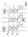
- FIG. 2is a block diagram and schematic of a memory system in accordance with the present invention.
- FIGS. 3A, 3B , and 3 Care schematics of alternative versions of a repair enable circuit in the memory system of FIG. 2 ;
- FIG. 4is a block diagram of a modified version of the memory system of FIG. 2 ;
- FIG. 5is a diagram of a semiconductor wafer including an integrated circuit die incorporating the memory system of FIG. 2 ;
- FIG. 6is a block diagram of an electronic system including a memory device incorporating the memory system of FIG. 2 .
- the present inventionprovides an improved device and method for repairing Dynamic Random Access Memory (DRAM) arrays and other memory arrays.
- the device and methodrepair arrays that, for example, contain memory cells that are defective as a result of being unable to retain an electric charge representing a “1” or “0” bit that is sufficient to cause a detectable change in voltage on a digit line when discharged to the digit line.
- the device and methodstore an electric charge representing an individual “1” or “0” bit in multiple memory cells in an array that share a pair of complementary digit lines.
- the electric charges stored in the multiple memory cellsare discharged to the pair of digit lines, causing a detectable change in voltage on the digit lines.
- the device and methodthus “gang” memory cells together to repair an array.
- an inventive memory system 30includes row and column address buffers 32 and 34 , respectively, receiving a multiplexed Memory Address, a row address strobe signal RAS*, and a column address strobe signal CAS*.
- the address buffers 32 and 34may comprise any circuitry for buffering memory addresses, including, for example, pre-decoders and array buffers.
- the present inventionis applicable to memory systems receiving any number of address bits in any configuration, including both multiplexed and non-multiplexed addressing schemes.
- a “multiplexed” Memory Addressis an address that is provided to a memory system in the form of a first plurality of address bits (e.g., the row address bits in a typical DRAM system) followed in time by a second plurality of address bits (e.g., the column address bits in a typical DRAM system).
- the memory system 30operates in both an unrepaired state and a repaired state.
- the row address buffers 32In its unrepaired state, in response to RAS* being activated, the row address buffers 32 operate in a well known manner to latch in a first plurality of address bits A 0 , A 1 , . . . , and Az from the Memory Address and then output a corresponding Row Address that includes row address bits RA 0 , RA 1 , . . . , RAz.
- a sense amplifier ( 0 )also equilibrates voltages on a pair of complementary digit lines D 0 and D 0 * to the cell plate voltage DVC 2 .
- a repair enable circuit 36is configured in the unrepaired state to allow normal operation of the memory system 30 by outputting a high, inactive repair enable signal REP_EN* to inputs of first and second NAND gates 38 and 40 , respectively.
- REP_EN*inactive repair enable signal
- the first NAND gate 38outputs a low, inactive odd row decoder enabling signal 0 _EN to disable an odd row decoder 42 and, at the same time, an inverter 44 outputs a low, causing the second NAND gate 40 to output a high, active even row decoder enabling signal E_EN to enable an even row decoder 46 .
- the enabled even row decoder 46then energizes one of a plurality of even word lines (i.e., rows) WL 0 and WL 2 in a DRAM array 48 selected in accordance with the row address bits RA 1 , . . . , RAz in a well known manner.
- the first NAND gate 38When, instead, the row address bit RA 0 is low, the first NAND gate 38 outputs a high, active odd row decoder enabling signal O_EN to enable the odd row decoder 42 and, at the same time, the inverter 44 outputs a high, causing the second NAND gate 40 to output a low, inactive even row decoder enabling signal E_EN to disable the even row decoder 46 .
- the enabled odd row decoder 42then energizes one of a plurality of odd word lines WL 1 and WL 3 selected in accordance with the row address bits RA 1 , . . . , RAz in a well known manner.
- the repair enable circuit 36may comprise any circuitry for enabling repair of an array, including, for example, fuses or anti-fuses.
- “configure,” “configuring,” and “configured,”include both an affirmative act with respect to a circuit (e.g., blowing a fuse or an anti-fuse) and the absence of an affirmative act with respect to the circuit (e.g., not blowing a fuse or an anti-fuse).
- the present inventionis not limited to enabling circuitry including the repair enable circuit 36 and first and second NAND gates 38 and 40 .
- the present inventionincludes within its scope any circuitry capable of enabling repair of an array.
- the row decoders 42 and 46may comprise any word line energizing circuitry, including, for example, phase drivers and word line drivers. Still further, it will be understood that while only four word lines are shown in FIG. 2 for purposes of clarity, any number of word lines will work for purposes of the present invention. Also, it will be understood that while the present invention is described with respect to the DRAM array 48 , the present invention is applicable to other memory arrays.
- the even word line WL 0is energized, as described above, in the unrepaired state of the memory system 30 , the energized even word line WL 0 activates an NMOS transistor 50 in a memory cell 52 in the DRAM array 48 through a control terminal 53 of the NMOS transistor 50 .
- the DRAM array 48is shown in FIG. 2 as having only four memory cells for clarity, it will be understood that the DRAM array 48 includes millions of memory cells, and that the present invention is applicable to arrays including any number of memory cells.
- an access terminal 55e.g., a digit line contact
- the DRAM array 48includes a multitude of digit lines and sense amplifiers, and that the present invention includes within its scope any number of digit lines and sense amplifiers.
- the storage capacitor 54When the storage capacitor 54 is connected to the digit line D 0 through the activated NMOS transistor 50 and the access terminal 55 , the storage capacitor 54 discharges its positive electric charge to the digit line D 0 . As a result, a voltage on the digit line D 0 rises by V SENSE as calculated above.
- the column address buffers 34operate in a well-known manner to latch in a second plurality of address bits A 0 , A 1 , . . . , and Az from the Memory Address and then output a corresponding Column Address to a column decoder 56 .
- the sense amplifier ( 0 )detects the change in voltage V SENSE and, in response, drives the digit line D 0 to the supply voltage V CC and the digit line D 0 * approximately to the reference voltage V SS .
- the column decoder 56then energizes a column select signal CSEL_ 0 selected in accordance with the Column Address in a well-known manner, thereby activating a pair of input/output gating NMOS transistors 58 and 60 .
- the voltages on the digit lines D 0 and D 0 *are transferred through an input/output bus ⁇ I/O, I/O*>to a data buffer 62 , including well-known DC sense amplifiers 64 , an output buffer 66 , write drivers 68 , and an input buffer 70 .
- the data buffer 62then outputs the “1” bit as an output data signal Q to external circuitry (not shown).
- external circuitrynot shown.
- the present inventionis not limited to data buffers including DC sense amplifiers, output buffers, write drivers, and input buffers.
- the sense amplifier ( 0 )does not detect the change in voltage V SENSE , and the voltages on the digit lines D 0 and D 0 * do not separate as desired.
- the “1” bit (and any other bit) stored on the storage capacitor 54is irretrievable, and the memory system 30 requires repair.
- the word line WL 3may comprise a redundant word line so that the failing memory cell 52 is replaced with a memory cell 72 along the word line WL 3 .
- conventional methodsare not always successful.
- Refresh counter circuitry 73such as a CBR (CAS Before RAS) refresh counter, is operative in a well-known manner in the unrepaired state of the memory system 30 .
- CBRCAS Before RAS
- Repair of the memory system 30is enabled in accordance with the present invention by configuring the repair enable circuit 36 to output a low, active repair enable signal REP_EN* to inputs of the first and second NAND gates 38 and 40 .
- the first NAND gate 38outputs a high, active odd row decoder enabling signal 0 _EN to enable the odd row decoder 42 .
- the second NAND gate 40also outputs a high, active even row decoder enabling signal E_EN to enable the even row decoder 46 .
- the row address buffers 32operate in the same well-known manner to latch in the first plurality of address bits A 0 , A 1 , . . . , and Az from the Memory Address and then output a corresponding Row Address that includes row address bits RA 0 , RA 1 , . . . , RAz.
- the sense amplifier ( 0 )also equilibrates the voltages on the digit lines D 0 and D 0 * to the cell plate voltage DVC 2 .
- the even row decoder 46Because the even row decoder 46 is enabled in the repaired state of the memory system 30 as described above, it energizes an even word line WL 0 or WL 2 selected in accordance with the row address bits RA 1 , . . . , RAz. As a result, the NMOS transistor 50 or an NMOS transistor 74 is activated, connecting the storage capacitor 54 or a storage capacitor 76 , respectively, to the respective digit line D 0 or D 0 * through the activated NMOS transistor 50 or 74 and the access terminal 55 or an access terminal 77 (e.g., a digit line contact).
- the odd row decoder 42because the odd row decoder 42 is also enabled in the repaired state, it energizes an odd word line WL 1 or WL 3 also selected in accordance with the row address bits RA 1 , . . . , RAz. As a result, an NMOS transistor 78 or 80 is activated, connecting a respective storage capacitor 82 or 84 to the respective digit line D 0 or D 0 * through the activated NMOS transistor 78 or 80 and the respective access terminal 55 or 77 .
- the memory system 30can store a “1” or “0” bit on the connected capacitors.
- the input buffer 70directs the write drivers 68 to drive the input/output bus ⁇ I/O, I/O*>to the supply voltage V CC (I/O) and approximately to the reference voltage V SS (I/O*).
- the column address buffers 34operate in the same well-known manner to latch in the second plurality of address bits A 0 , A 1 , . . . , Az from the Memory Address and output a corresponding Column Address to the column decoder 56 .
- the column decoder 56energizes the column select signal CSEL_ 0 selected in accordance with the Column Address, thereby activating the input/output gating NMOS transistors 58 and 60 and conducting the input/output bus ⁇ I/O, I/O*>voltages to the sense amplifier ( 0 ).
- the sense amplifier ( 0 )responds by driving the digit lines D 0 and D 0 * to the respective supply voltage V CC and reference voltage V SS . These voltages are then stored as described above on two of the storage capacitors 54 , 76 , 82 , and 84 that are each connected to one of the digit lines D 0 and D 0 *.
- the memory system 30can also retrieve a “1” or “0” bit stored on two of the storage capacitors 54 , 76 , 82 , and 84 .
- the even and odd row decoders 46 and 42respectively, energize one of the even word lines WL 0 and WL 2 and one of the odd word lines WL 1 and WL 3 each selected in accordance with the row address bits RA 1 , . . . , RAz as described above.
- positive electric charges representing a “1” bit stored on the storage capacitors 54 and 82may discharge through respective NMOS transistors 50 and 78 activated by respective energized word lines WL 0 and WL 1 .
- the “1” bitmay be successfully retrieved through the sense amplifier ( 0 ), the input/output gating NMOS transistors 58 and 60 , the input/output bus ⁇ I/O, I/O*>, and the data buffer 62 in the manner described above.
- the memory system 30including any previously defective memory cells, is repaired.
- the present inventionworks with two or more memory cells connected to the same digit line D 0 or D 0 *, for example, as described above, and with one or more memory cells connected to the digit line D 0 and one or more memory cells connected to the digit line D 0 *. Further, it should be understood that while the memory system 30 has been described as including both odd and even row decoders 42 and 46 , the present invention includes within its scope any decoding circuitry capable of energizing two or more word lines in accordance with each Memory Address.
- the present inventionincludes within its scope the energizing of a different number of word lines for different row addresses (e.g., energizing two word lines for a first row address and four word lines for a second row address). Such a scheme may be desirable where more memory cells are necessary to repair an array in some locations than in others.
- the memory system 30has less total storage capacity in its repaired state than in its unrepaired state. For example, if the memory system 30 is provided in a 16-Megabit ⁇ 1 configuration in its unrepaired state, it has 2 12 uniquely addressable word lines (i.e., rows) and 2 12 uniquely addressable pairs of digit lines (i.e., columns) for a total of 2 24 uniquely addressable locations (i.e., memory cells). If the memory system 30 is then repaired in accordance with the present invention by enabling the accessing of two memory cells for each received memory address, the repaired memory system 30 has 2 11 uniquely addressable pairs of word lines and 212 uniquely addressable pairs of digit lines for a total of 2 23 uniquely addressable locations (i.e., pairs of memory cells).
- the repaired memory system 30is in an 8-Megabit ⁇ 1 configuration. If, instead, the memory system 30 is repaired by enabling the accessing of four memory cells for each received memory address, the repaired memory system 30 has 2 10 uniquely addressable groups of four word lines and 212 uniquely addressable pairs of digit lines for a total of 2 22 uniquely addressable locations (i.e., groups of four memory cells). As a result, the repaired memory system 30 is in a 4-Megabit ⁇ 1 configuration.
- the even and odd row decoders 46 and 42are each configurable with, for example, fuses or anti-fuses, to select and energize two word lines in accordance with each row address.
- accessingmeans energizing a conductor, such as a word line, connected to an access terminal of the cell, and then sensing a resulting change in voltage on the conductor using a sense amplifier.
- accessingthus includes both refreshing and reading a memory cell.
- the 4-Megabit ⁇ 1 configuration produced in the above example by grouping four word lines together for each memory addressis an industry standard configuration and the 8-Megabit ⁇ 1 configuration is not, it can be seen that it can be advantageous to group four word lines together when repairing the memory system 30 in accordance with the present invention.
- the same advantageous principleapplies to grouping sixteen, sixty-four, etc., word lines together when repairing the memory system 30 in accordance with the present invention.
- 8-Megabit, 32-Megabit, 128-Megabit, etc., configurationscan be useful, for example, in producing standard Single In-Line Memory Module (SIMM) upgrade configurations.
- SIMMSingle In-Line Memory Module
- the column address buffers 34continue to receive the twelve address bits with each memory address that they received in the 16-Megabit ⁇ 1 configuration. This is because in both the unrepaired 16-Megabit ⁇ 1 configuration and the repaired 4-Megabit ⁇ 1 configuration, the memory system 30 has 2 12 uniquely addressable pairs of digit lines. Allowing the column address buffers 34 to continue to receive twelve address bits in the repaired 4-Megabit ⁇ 1 configuration can be problematic, though, because standard die packages for 4-Megabit ⁇ 1 dice include only eleven address bit terminals.
- the column address buffers 34 in the memory system 30are preferably configurable with, for example, fuses or anti-fuses, to latch in an address bit in the first eleven address bits from the Memory Address in response to RAS* being activated.
- the row address buffers 32latch in the other ten address bits from the Memory Address in response to RAS* being activated in order to be able to uniquely address the 2 10 groups of four word lines in the memory system 30 .
- the column address buffers 34latch in the second eleven address bits from the Memory Address in order to have a total of twelve address bits from the Memory Address to uniquely address the 2 12 pairs of complementary digit lines in the memory system 30 .
- the refresh counter circuitry 73 of the memory system 30may be configured with fuses, anti-fuses, or the like to output row addresses in the repaired state of the memory system 30 , which correspond appropriately to those addresses output by the row address buffers 32 .
- the repair enable circuit 36includes a plurality of fuses 86 that are configurable to cause the repair enable circuit 36 to output the low, active repair enable signal REP_EN*.
- the fuses 86may be configured in a well-known manner by laser or electric current.
- the repair enable circuit 36includes a plurality of anti-fuses 88 that are also configurable to cause the repair enable circuit 36 to output the low, active repair enable signal REP_EN*.
- the anti-fuses 88may be configured in a well-known manner with a programming voltage. As shown in FIG.
- the repair enable circuit 36is configurable in response to a test mode enable signal TEST_EN from external circuitry (not shown) to cause the repair enable circuit 36 to output the low, active repair enable signal REP_EN*.
- TEST_ENtest mode enable signal
- REP_EN*active repair enable signal
- FIG. 4A modified version of the memory system 30 of FIG. 2 is shown in FIG. 4 .
- row and column address buffers 90 and 92respectively, receive a non-multiplexed memory address 94 in the repaired, 4-Megabit ⁇ 1 state of the memory system 30 .
- the memory address 94includes row address bits R 0 , . . . , and R 9 provided through row address bit die bond pads 96 and column address bits C 0 , C 1 , . . . , C 11 provided through column address bit die bond pads 98 and one of the row address bit die bond pads 96 .
- the column address buffers 92receive the twelve address bits necessary to uniquely address the 2 12 pairs of digit lines in the memory system 30
- the row address buffers 90receive the ten address bits necessary to uniquely address the 2 10 groups of four word lines in the memory system 30 .
- the memory system 30is recovered from its unrepaired 16-Megabit ⁇ 1 configuration in a repaired 4-Megabit ⁇ 1 configuration that is pin compatible with the eleven standard pins in 4-Megabit die packages.
- the unrepaired, 16-Megabit ⁇ 1 configuration and repaired, 4-Megabit ⁇ 1 configuration for the memory system 30 described aboveare only examples, and that the present invention is therefore not so limited.
- a semiconductor wafer 100includes a yet-to-be cut integrated circuit die 102 that incorporates the memory system 30 of FIG. 2 .
- an electronic system 104includes an input device 106 , an output device 108 , and a memory device 110 , all coupled to a processor device 112 .
- the memory device 110incorporates the memory system 30 of FIG. 2 .
- the present inventionthus provides an improved device and method for repairing DRAM and other memory arrays.
- the present inventionwhen applied to a DRAM array effectively halves the time it takes to refresh the array.
- the present inventionalso reduces the time T RAC in a DRAM array from the activation of RAS* to the outputting of valid data because the greater charge applied by the present invention to the array's digit lines for each “1” or “0” bit retrieved from the array allows the sense amplifiers in the array to more quickly detect a bit being retrieved.
- the greater charge applied by the present invention to a DRAM array's digit lines for each “1” or “0” bit retrieved from the arraymakes the retrieval of bits from the array less sensitive to fluctuations in the supply voltage V CC and the reference voltage V SS .
Landscapes
- Engineering & Computer Science (AREA)
- Microelectronics & Electronic Packaging (AREA)
- Computer Hardware Design (AREA)
- For Increasing The Reliability Of Semiconductor Memories (AREA)
- Dram (AREA)
Abstract
Description
- This application is a continuation of application Ser. No. 10/928,380, filed Aug. 27, 2004, pending, which is a continuation of application Ser. No. 10/395,478, filed Mar. 24, 2003, now U.S. Pat. No. 6,853,601, issued Feb. 8, 2005, which is a continuation of application Ser. No. 10/189,138, filed Jul. 2, 2002, now U.S. Pat. No. 6,538,949, issued Mar. 25, 2003, which is a continuation of application Ser. No. 09/886,762, filed Jun. 21, 2001, now U.S. Pat. No. 6,442,094, issued Aug. 27, 2002, which is a continuation of application Ser. No. 09/618,816, filed Jul. 18, 2000, now U.S. Pat. No. 6,285,618, issued Sept. 4, 2001, which is a continuation of application Ser. No. 09/015,541, filed Jan. 29, 1998, now U.S. Pat. No. 6,122,213, issued Sept. 19, 2000, which is a divisional of application Ser. No. 08/775,510, filed Dec. 31, 1996, now U.S. Pat. No. 5,781,483, issued Jul. 14, 1998.
- 1. Field of the Invention The present invention relates in general to memory array repair and, in particular, to devices and methods for repairing memory arrays, such as dynamic random access memory arrays, by storing each individual bit in multiple memory cells in the arrays.
- 2. State of the Art In general, Dynamic Random Access Memory (DRAM) arrays store digital information in the form of “1” and “0” bits by storing the bits as electric charges on capacitors. DRAM arrays then retrieve the stored bits by discharging their representative electric charges to a conductor, such as a digit line, and then detecting a change in voltage on the conductor resulting from the discharge. When any of the capacitors in a DRAM array are unable to store a sufficient electric charge to cause a detectable change in voltage on a conductor when discharged to the conductor, any “1” or “0” bits stored as electric charges on those capacitors cannot be retrieved by the array. In this circumstance, the array must be repaired by replacing the failing capacitors with redundant capacitors in redundant rows or columns in the array. If too many of the redundant capacitors also fail, then the array must be discarded.
- More specifically, a
conventional DRAM array 10 shown inFIG. 1 stores digital information in the form of “1” and “0” bits by storing the bits as electric charges onstorage capacitors memory cells DRAM array 10 is shown inFIG. 1 as having only nine memory cells in order to simplify description, theDRAM array 10 typically includes thousands or millions of memory cells. - The
DRAM array 10 stores a “1” bit in thememory cell 18, for example, by energizing the word line WL0 to activate anNMOS transistor 26. TheDRAM array 10 then applies a “1” bit voltage equal to a supply voltage VCC(e.g., 3.3 Volts) to the digit line D0, causing current to flow from the digit line D0, through the activatedNMOS transistor 26 and thestorage capacitor 12, and to a cell plate voltage DVC2 typically equal to one half the supply voltage VCC. As this current flows, thestorage capacitor 12 stores positive electric charge received from the digit line D0, causing a voltage VS1, on thestorage capacitor 12 to increase. When the voltage VS1, on thestorage capacitor 12 equals the “1” bit voltage on the digit line D0, current stops flowing through thestorage capacitor 12. A short time later, theDRAM array 10 de-energizes the word line WL0 to de-activate theNMOS transistor 26 and isolate thestorage capacitor 12 from the digit line D0, thereby preventing the positive electric charge stored on thestorage capacitor 12 from discharging back to the digit line D0. - Similarly, the
DRAM array 10 stores a “0” bit in thememory cell 20, for example, by energizing the word line WL1 to activate anNMOS transistor 28. TheDRAM array 10 then applies a “0” bit voltage approximately equal to a reference voltage VSS(e.g., 0.0 Volts) to the digit line D0, causing current to flow from the cell plate voltage DVC2, through thestorage capacitor 14 and the activatedNMOS transistor 28, and to the digit line D0. As this current flows, thestorage capacitor 14 stores negative electric charge received from the digit line D0, causing a voltage VS2on thestorage capacitor 14 to decrease. When the voltage VS2equals the “0” bit voltage on the digit line D0, current stops flowing through thestorage capacitor 14. A short time later, theDRAM array 10 de-energizes the word line WL1 to de-activate theNMOS transistor 28 and isolate thestorage capacitor 14 from the digit line D0, thereby preventing the negative electric charge stored on thestorage capacitor 14 from discharging back to the digit line D0. - The
DRAM array 10 stores “1” and “0” bits in thememory cells 22 arranged along the complementary digit lines D0*, D1*, . . . , and Dn* in a manner similar to that described above, with the exception that the “1” bit voltage for these cells is approximately equal to the reference voltage VSSand the “0” bit voltage equals the supply voltage VSS. - The
DRAM array 10 retrieves “1” and “0” bits stored in the manner described above in thememory cells storage capacitors - For example, the
DRAM array 10 retrieves the “1” bit stored in thememory cell 18 by first equilibrating the voltages on the digit lines D0 and D0* to the cell plate voltage DVC2. TheDRAM array 10 then energizes the word line WL0 to activate theNMOS transistor 26, causing the positive electric charge stored on thestorage capacitor 12 to discharge through the activatedNMOS transistor 26 to the digit line D0. As the positive electric charge discharges, the voltage on the digit line D0 rises by an amount VSENSEcalculated as follows:
VSENSE=(VS−DVC2)*CS/(CD+CS)
where VSis the voltage VS1on thestorage capacitor 12, CSis the capacitance of thestorage capacitor 12, and CDis the capacitance of the digit line D0. When the rise in voltage VSENSEon the digit line D0 causes a difference in voltages between the digit lines D0 and D0* to exceed a detection threshold (typically about 150 m Volts) of the sense amplifier (0), the sense amplifier (0) responds by driving the voltage on the digit line D0 to the supply voltage VCCand by driving the voltage on the digit line D0* approximately to the reference voltage VSS. Input/output gating circuitry, DC sense amplifiers, and an output buffer (not shown) then transmit these voltages from the digit lines D0 and D0* to external circuitry as a “1” bit. - Likewise, the
DRAM array 10 retrieves the “0” bit stored in thememory cell 20, for example, by first equilibrating the voltages on the digit lines D0 and D0* to the cell plate voltage DVC2. TheDRAM array 10 then energizes the word line WL1 to activate theNMOS transistor 28, causing the negative electric charge stored on thestorage capacitor 14 to discharge through the activatedNMOS transistor 28 to the digit line D0. As the negative electric charge discharges, the voltage on the digit line D0 falls by an amount VSENSE, calculated as described above, where VSis the voltage VS2on thestorage capacitor 14 and CSis the capacitance of thestorage capacitor 14. When the drop in voltage VSENSEon the digit line D0 causes the difference in voltages between the digit lines D0 and D0* to exceed the detection threshold of the sense amplifier (0), the sense amplifier (0) responds by driving the voltage on the digit line D0 approximately to the reference voltage VSSand by driving the voltage on the digit line D0* to the supply voltage VCC. The input/output gating circuitry, DC sense amplifiers, and output buffer then transmit these voltages from the digit lines D0 and D0* to external circuitry as a “0” bit. - The
DRAM array 10 retrieves “1” and “0” bits from thememory cells 22 arranged along the complementary digit lines D0*, D1*, . . . , and Dn* in the same manner as described above. - DRAM arrays sometimes contain defective memory cells that are unable to reliably store “1” and “0” bits in the manner described above. In some instances, this occurs because the capacitance of the storage capacitors in these memory cells is too small, preventing the capacitors from retaining a sufficient electric charge to cause a change in voltage VSENSEon a digit line when discharged to the digit line that exceeds a sense amplifier's detection threshold. In other instances, this occurs because the electric charge stored on the storage capacitors in these memory cells leaks away through a variety of mechanisms, also preventing the capacitors from retaining a sufficient electric charge to cause a detectable change in voltage VSENSEon a digit line when discharged to the digit line. In either case, because the change in voltage VSENSEcaused by discharging the electric charges stored by the storage capacitors in these memory cells cannot be detected by a sense amplifier, the “1” and “0” bits represented by the electric charges stored in these memory cells are irretrievable.
- DRAM arrays are also sometimes unable to reliably store “1” and “0” bits in certain memory cells because the detection threshold of the cells'associated sense amplifier is too large for the sense amplifier to detect a change in voltage VSENSEcaused by one of the cells discharging to the digit line. In this case as well, the “1” and “0” bits represented by the electric charges stored in these cells are irretrievable.
- Generally, when DRAM arrays are found to be defective in this way, an attempt is made to repair the arrays by replacing defective memory cells and defective sense amplifiers in the arrays with redundant memory cells provided in redundant rows or columns in the arrays and with redundant sense amplifiers provided in the redundant columns.
- Conventionally, when a redundant row is used to repair a DRAM array containing a defective memory cell, a row address that identifies the defective cell's row is permanently stored in the array by blowing selected fuses or anti-fuses in the array. Then, during normal operation of the DRAM array, if the array receives a request to access a memory cell having a memory address including a row address portion that corresponds to the stored row address, redundant circuitry in the array directs the array to access a redundant memory cell in the redundant row instead of accessing the memory cell identified by the received memory address. Since every memory cell in the defective cell's row has the same row address, every cell in the defective cell's row, both operative and defective, is replaced by a redundant memory cell in the redundant row.
- Similarly, when a redundant column is used to repair a DRAM array containing a defective memory cell, a column address that identifies the defective cell's column is permanently stored in the array by blowing selected fuses or anti-fuses in the array. Then, during normal operation of the DRAM array, if the array receives a request to access a memory cell having a memory address including a column address portion that corresponds to the stored column address, redundant circuitry in the array directs the array to access a redundant memory cell in the redundant column instead of accessing the memory cell identified by the received memory address. Since every memory cell in the defective cell's column has the same column address, every cell in the defective cell's column, both operative and defective, is replaced by a redundant memory cell in the redundant column.
- The process described above for repairing a DRAM array using redundant rows and columns is well known in the art, and is described in various forms in U.S. Pat. No. Nos. 4,459,685, 4,601,019, 5,422,850 and 5,528,539.
- Because the conventional repair process described above uses an entire redundant row or column to repair each defective memory cell in a DRAM or other memory array, the number of defective memory cells that can be repaired in an array is limited by the number of redundant rows or columns in the array which, in turn, is limited by the space available in the array for redundant rows or columns. As a result, it is not uncommon for defective DRAM and other memory arrays to be discarded because the conventional repair process cannot repair the quantity of defective memory cells they contain. This problem is often exacerbated by the discovery of defective redundant memory cells in the available redundant rows or columns. Obviously, it would be preferable to be able to repair these defective arrays rather than discard them.
- Therefore, there is a need in the art for an improved device and method for repairing DRAM arrays and other memory arrays. Such an improved device and method should be applicable to arrays containing memory cells that are unable to reliably store “1” and “0” bits because their storage capacitors do not retain a sufficient electric charge, or because their associated sense amplifiers have a detection threshold that is too large.
- The present invention provides an apparatus for repairing a memory array, such as a DRAM array, that includes a pair of complementary digit lines through which memory cells activated by word lines selected in accordance with row addresses are accessed. The array may need repair, for example, when a memory cell in the array is unable to properly store “1” and “0” bits because the charge it retains representing a bit is not sufficient to cause a detectable change in voltage on one of the digit lines when discharged to the digit line.
- When repair is needed, enabling circuitry (e.g., fuses or anti-fuses) in the apparatus enables repair of the array, and word line energizing circuitry (e.g., a row decoder) responsive to the enabling circuitry energizes more than one word line in the array in accordance with each row address so that more than one memory cell is accessed through the digit lines for each row address. As a result, the apparatus stores a single “1” or “0” bit as a charge in multiple memory cells. Then, when the apparatus retrieves the single bit, the bit's representative charges stored in the multiple memory cells are discharged to the digit lines to cause a change in voltage on the digit lines that is greater than and, therefore, more likely to be detectable than a change in voltage on the digit lines caused by discharging a representative charge stored in a single memory cell to the digit lines in the conventional manner.
- In other embodiments of the present invention, a memory system, an integrated circuit die, and a semiconductor wafer include the repair apparatus and memory array described above. In another embodiment, an electronic system includes input, output, processor, and memory devices, and the memory device includes the repair apparatus and memory array described above.
- In a further embodiment, the present invention provides an apparatus for repairing a memory array. The memory array is of the type in which stored bits are read by detecting a change in voltage between two conductors caused by sharing a charge stored in a memory cell in the array with one of the conductors. The apparatus repairs the array when some memory cells in the array cannot retain a sufficient charge to cause a detectable change in voltage on one of the conductors. The apparatus includes circuitry directing each memory cell in a group of cells in the array to store a charge representing a single stored bit and, when the single stored bit is being read, to share its stored charge with one of the conductors.
- In a still further embodiment, the present invention provides an apparatus for repairing a memory array. The memory array is of the type in which stored bits are accessed by using sense amplifiers to detect a change in voltage between two conductors caused by sharing a charge stored in a memory cell in the array with one of the conductors. The apparatus repairs the array when some of the sense amplifiers in the array cannot detect a change in voltage on one of the conductors caused by sharing a charge stored in one of the memory cells with one of the conductors. The apparatus includes circuitry directing each memory cell in a group of cells in the array to store a charge representing a single stored bit and, when the single stored bit is being accessed, to share its stored charge with one of the conductors.
- In an additional embodiment, a memory system includes a memory array including pairs of complementary digit lines, alternating even and odd word lines, and memory cells controlled by the word lines and accessed through the digit lines. Address buffers receive memory addresses and output corresponding row and column addresses, and row decoder circuitry energizes at least two word lines in accordance with each row address. A column decoder outputs a column select signal in accordance with each column address, and sense amplifier and input/output gating circuitry selects a pair of complementary digit lines in the array in accordance with each column select signal. As a result, two or more memory cells that are each controlled by one of the energized word lines are accessed through one of the selected digit lines. A data buffer provides communication between the accessed memory cells and external circuitry.
- In a further embodiment, a memory system includes a memory array including pairs of complementary digit lines, word lines, and memory cells controlled by the word lines and accessed through the digit lines. Address buffers receive multiplexed memory addresses in the form of a first plurality of address bits followed in time by a second plurality of address bits. The address buffers also output a row address and a first portion of a column address corresponding to each memory address'associated first plurality of address bits, and output a second portion of the column address corresponding to each memory address'associated second plurality of address bits. Row decoder circuitry energizes at least two word lines in accordance with each row address, and a column decoder outputs a column select signal in accordance with the first and second portions of each column address. Sense amplifier and input/output gating circuitry selects a pair of complementary digit lines in the array in accordance with each column select signal so at least two memory cells controlled by the energized word lines are accessed through one of the selected digit lines. As a result, the accessed memory cells together may store or output a single memory bit to external circuitry. A data buffer provides communication between the accessed memory cells and external circuitry.
- In a still further embodiment, a memory system includes a memory array including pairs of complementary digit lines, word lines, and memory cells controlled by the word lines and accessed through the digit lines. Row address bit terminals receive a first plurality of address bits associated with a non-multiplexed memory address, and column address bit terminals receive a second plurality of address bits associated with the non-multiplexed memory address. Address buffers output a row address corresponding to a first portion of the first plurality of address bits and output a column address corresponding to both the second plurality of address bits and a second portion of the first plurality of address bits. Row decoder circuitry energizes at least two word lines in accordance with the row address, and a column decoder outputs a column select signal in accordance with the column address. Sense amplifier and input/output gating circuitry selects a pair of complementary digit lines in the array in accordance with the column select signal. As a result, at least two memory cells controlled by the energized word lines are accessed through one of the selected digit lines. A data buffer provides communication between the accessed memory cells and external circuitry.
- In a still additional embodiment, a method for storing a bit in a memory array having a plurality of memory cells each coupled to one of a pair of complementary digit lines includes providing a charge representing the bit on each of the digit lines, storing the charge provided on one of the digit lines in at least one of the memory cells, and storing the charge provided on one of the digit lines in at least one other of the memory cells.
- In another embodiment, a method of testing a repair for a memory array of the type to store a bit by storing a charge in a memory cell, and also of the type to access the bit by sharing the stored charge with one of two conductors and then detecting a resulting change in voltage between the conductors, comprises: directing the memory cells in a group of memory cells in the memory array to each store the same bit by each storing a charge representing the bit; directing each memory cell in the group of memory cells to share its stored charge with one of the conductors; and attempting to detect a change in voltage between the conductors resulting from the memory cells in the group sharing their stored charges with the conductors.
FIG. 1 is a schematic of a conventional dynamic random access memory array;FIG. 2 is a block diagram and schematic of a memory system in accordance with the present invention;FIGS. 3A, 3B , and3C are schematics of alternative versions of a repair enable circuit in the memory system ofFIG. 2 ;FIG. 4 is a block diagram of a modified version of the memory system ofFIG. 2 ;FIG. 5 is a diagram of a semiconductor wafer including an integrated circuit die incorporating the memory system ofFIG. 2 ; andFIG. 6 is a block diagram of an electronic system including a memory device incorporating the memory system ofFIG. 2 .- In general, the present invention provides an improved device and method for repairing Dynamic Random Access Memory (DRAM) arrays and other memory arrays. The device and method repair arrays that, for example, contain memory cells that are defective as a result of being unable to retain an electric charge representing a “1” or “0” bit that is sufficient to cause a detectable change in voltage on a digit line when discharged to the digit line.
- The device and method store an electric charge representing an individual “1” or “0” bit in multiple memory cells in an array that share a pair of complementary digit lines. When a bit stored in this inventive manner is retrieved, the electric charges stored in the multiple memory cells are discharged to the pair of digit lines, causing a detectable change in voltage on the digit lines. The device and method thus “gang” memory cells together to repair an array.
- More particularly, as shown in
FIG. 2 , aninventive memory system 30 includes row and column address buffers32 and34, respectively, receiving a multiplexed Memory Address, a row address strobe signal RAS*, and a column address strobe signal CAS*. It will be understood by those having skill in the field of this invention that the address buffers32 and34 may comprise any circuitry for buffering memory addresses, including, for example, pre-decoders and array buffers. Also, it will be understood that the present invention is applicable to memory systems receiving any number of address bits in any configuration, including both multiplexed and non-multiplexed addressing schemes. Further, as used herein, a “multiplexed” Memory Address is an address that is provided to a memory system in the form of a first plurality of address bits (e.g., the row address bits in a typical DRAM system) followed in time by a second plurality of address bits (e.g., the column address bits in a typical DRAM system). - The
memory system 30 operates in both an unrepaired state and a repaired state. In its unrepaired state, in response to RAS* being activated, the row address buffers32 operate in a well known manner to latch in a first plurality of address bits A0, A1, . . . , and Az from the Memory Address and then output a corresponding Row Address that includes row address bits RA0, RA1, . . . , RAz. A sense amplifier (0) also equilibrates voltages on a pair of complementary digit lines D0 and D0* to the cell plate voltage DVC2. - In addition, a repair enable
circuit 36 is configured in the unrepaired state to allow normal operation of thememory system 30 by outputting a high, inactive repair enable signal REP_EN* to inputs of first andsecond NAND gates first NAND gate 38 outputs a low, inactive odd row decoder enabling signal0_EN to disable anodd row decoder 42 and, at the same time, aninverter 44 outputs a low, causing thesecond NAND gate 40 to output a high, active even row decoder enabling signal E_EN to enable aneven row decoder 46. The enabled even rowdecoder 46 then energizes one of a plurality of even word lines (i.e., rows) WL0 and WL2 in aDRAM array 48 selected in accordance with the row address bits RA1, . . . , RAz in a well known manner. - When, instead, the row address bit RA0 is low, the
first NAND gate 38 outputs a high, active odd row decoder enabling signal O_EN to enable theodd row decoder 42 and, at the same time, theinverter 44 outputs a high, causing thesecond NAND gate 40 to output a low, inactive even row decoder enabling signal E_EN to disable theeven row decoder 46. The enabledodd row decoder 42 then energizes one of a plurality of odd word lines WL1 and WL3 selected in accordance with the row address bits RA1, . . . , RAz in a well known manner. - As will be described in more detail below with respect to
FIGS. 3A, 3B , and3C, the repair enablecircuit 36 may comprise any circuitry for enabling repair of an array, including, for example, fuses or anti-fuses. Also, as used herein, “configure,” “configuring,” and “configured,” include both an affirmative act with respect to a circuit (e.g., blowing a fuse or an anti-fuse) and the absence of an affirmative act with respect to the circuit (e.g., not blowing a fuse or an anti-fuse). Further, it will be understood that the present invention is not limited to enabling circuitry including the repair enablecircuit 36 and first andsecond NAND gates row decoders FIG. 2 for purposes of clarity, any number of word lines will work for purposes of the present invention. Also, it will be understood that while the present invention is described with respect to theDRAM array 48, the present invention is applicable to other memory arrays. - If, for example, the even word line WL0 is energized, as described above, in the unrepaired state of the
memory system 30, the energized even word line WL0 activates anNMOS transistor 50 in amemory cell 52 in theDRAM array 48 through acontrol terminal 53 of theNMOS transistor 50. Of course, while theDRAM array 48 is shown inFIG. 2 as having only four memory cells for clarity, it will be understood that theDRAM array 48 includes millions of memory cells, and that the present invention is applicable to arrays including any number of memory cells. - As a result of the
NMOS transistor 50 being activated, astorage capacitor 54 storing a positive electric charge representing a “1” bit, for example, is connected to the digit line D0 through the activatedNMOS transistor 50 and an access terminal55 (e.g., a digit line contact). Of course, while only one pair of complementary digit lines D0 and D0* and only one sense amplifier (0) are shown inFIG. 2 for clarity, it will be understood that theDRAM array 48 includes a multitude of digit lines and sense amplifiers, and that the present invention includes within its scope any number of digit lines and sense amplifiers. - When the
storage capacitor 54 is connected to the digit line D0 through the activatedNMOS transistor 50 and theaccess terminal 55, thestorage capacitor 54 discharges its positive electric charge to the digit line D0. As a result, a voltage on the digit line D0 rises by VSENSEas calculated above. During the same period of time, in response to CAS* being activated, the column address buffers34 operate in a well-known manner to latch in a second plurality of address bits A0, A1, . . . , and Az from the Memory Address and then output a corresponding Column Address to acolumn decoder 56. - If the positive electric charge stored in the
storage capacitor 54 is sufficient for VSENSEto exceed a detection threshold of the sense amplifier (0), the sense amplifier (0) detects the change in voltage VSENSEand, in response, drives the digit line D0 to the supply voltage VCCand the digit line D0* approximately to the reference voltage VSS. Thecolumn decoder 56 then energizes a column select signal CSEL_0 selected in accordance with the Column Address in a well-known manner, thereby activating a pair of input/outputgating NMOS transistors data buffer 62, including well-knownDC sense amplifiers 64, anoutput buffer 66, writedrivers 68, and aninput buffer 70. Thedata buffer 62 then outputs the “1” bit as an output data signal Q to external circuitry (not shown). Of course, it will be understood that the present invention is not limited to data buffers including DC sense amplifiers, output buffers, write drivers, and input buffers. - If, instead, the positive electric charge stored in the
storage capacitor 54 is insufficient for VSENSEto exceed the detection threshold of the sense amplifier (0), or the detection threshold of the sense amplifier (0) is too large, the sense amplifier (0) does not detect the change in voltage VSENSE, and the voltages on the digit lines D0 and D0* do not separate as desired. As a result, the “1” bit (and any other bit) stored on thestorage capacitor 54 is irretrievable, and thememory system 30 requires repair. - If only a few memory cells in the
memory system 30 require repair, conventional methods using redundant rows and columns to replace these memory cells may work to repair thememory system 30. For example, the word line WL3 may comprise a redundant word line so that the failingmemory cell 52 is replaced with amemory cell 72 along the word line WL3. However, as described above, conventional methods are not always successful. Refresh counter circuitry 73, such as a CBR (CAS Before RAS) refresh counter, is operative in a well-known manner in the unrepaired state of thememory system 30.- Repair of the
memory system 30 is enabled in accordance with the present invention by configuring the repair enablecircuit 36 to output a low, active repair enable signal REP_EN* to inputs of the first andsecond NAND gates first NAND gate 38 outputs a high, active odd row decoder enabling signal0_EN to enable theodd row decoder 42. At the same time, thesecond NAND gate 40 also outputs a high, active even row decoder enabling signal E_EN to enable theeven row decoder 46. - In the repaired state of the
memory system 30, in response to RAS* being activated, the row address buffers32 operate in the same well-known manner to latch in the first plurality of address bits A0, A1, . . . , and Az from the Memory Address and then output a corresponding Row Address that includes row address bits RA0, RA1, . . . , RAz. The sense amplifier (0) also equilibrates the voltages on the digit lines D0 and D0* to the cell plate voltage DVC2. - Because the
even row decoder 46 is enabled in the repaired state of thememory system 30 as described above, it energizes an even word line WL0 or WL2 selected in accordance with the row address bits RA1, . . . , RAz. As a result, theNMOS transistor 50 or anNMOS transistor 74 is activated, connecting thestorage capacitor 54 or astorage capacitor 76, respectively, to the respective digit line D0 or D0* through the activatedNMOS transistor access terminal 55 or an access terminal77 (e.g., a digit line contact). At the same time, because theodd row decoder 42 is also enabled in the repaired state, it energizes an odd word line WL1 or WL3 also selected in accordance with the row address bits RA1, . . . , RAz. As a result, anNMOS transistor respective storage capacitor NMOS transistor respective access terminal - With two of the
storage capacitors memory system 30 can store a “1” or “0” bit on the connected capacitors. To store a “1” bit, for example, received by theinput buffer 70 as an input data signal D, theinput buffer 70 directs thewrite drivers 68 to drive the input/output bus <I/O, I/O*>to the supply voltage VCC(I/O) and approximately to the reference voltage VSS(I/O*). During the same period of time, in response to CAS* being activated, the column address buffers34 operate in the same well-known manner to latch in the second plurality of address bits A0, A1, . . . , Az from the Memory Address and output a corresponding Column Address to thecolumn decoder 56. In response, thecolumn decoder 56 energizes the column select signal CSEL_0 selected in accordance with the Column Address, thereby activating the input/outputgating NMOS transistors storage capacitors - Of course, the
memory system 30 can also retrieve a “1” or “0” bit stored on two of thestorage capacitors odd row decoders storage capacitors respective NMOS transistors storage capacitors gating NMOS transistors data buffer 62 in the manner described above. Thus, thememory system 30, including any previously defective memory cells, is repaired. - It should be understood that the present invention works with two or more memory cells connected to the same digit line D0 or D0*, for example, as described above, and with one or more memory cells connected to the digit line D0 and one or more memory cells connected to the digit line D0*. Further, it should be understood that while the
memory system 30 has been described as including both odd and even rowdecoders - It should also be understood that the
memory system 30 has less total storage capacity in its repaired state than in its unrepaired state. For example, if thememory system 30 is provided in a 16-Megabit×1 configuration in its unrepaired state, it has 212uniquely addressable word lines (i.e., rows) and 212uniquely addressable pairs of digit lines (i.e., columns) for a total of 224uniquely addressable locations (i.e., memory cells). If thememory system 30 is then repaired in accordance with the present invention by enabling the accessing of two memory cells for each received memory address, the repairedmemory system 30 has 211uniquely addressable pairs of word lines and212 uniquely addressable pairs of digit lines for a total of 223uniquely addressable locations (i.e., pairs of memory cells). As a result, the repairedmemory system 30 is in an 8-Megabit×1 configuration. If, instead, thememory system 30 is repaired by enabling the accessing of four memory cells for each received memory address, the repairedmemory system 30 has 210uniquely addressable groups of four word lines and212 uniquely addressable pairs of digit lines for a total of 222uniquely addressable locations (i.e., groups of four memory cells). As a result, the repairedmemory system 30 is in a 4-Megabit×1 configuration. Of course, in order to enable the accessing of four memory cells for each received memory address, the even andodd row decoders - It will be understood that, as used herein, “accessing” a memory cell means energizing a conductor, such as a word line, connected to an access terminal of the cell, and then sensing a resulting change in voltage on the conductor using a sense amplifier. The term “accessing” thus includes both refreshing and reading a memory cell.
- Since the 4-Megabit×1 configuration produced in the above example by grouping four word lines together for each memory address is an industry standard configuration and the 8-Megabit×1 configuration is not, it can be seen that it can be advantageous to group four word lines together when repairing the
memory system 30 in accordance with the present invention. This allows 256-Megabit arrays to be recovered (i.e., repaired) as industry standard 64-Megabit arrays, 64-Megabit arrays to be recovered as industry standard 16-Megabit arrays, 16-Megabit arrays to be recovered as industry standard 4-Megabit arrays, 4-Megabit arrays to be recovered as industry standard 1-Megabit arrays, etc. Of course, the same advantageous principle applies to grouping sixteen, sixty-four, etc., word lines together when repairing thememory system 30 in accordance with the present invention. - Of course, 8-Megabit, 32-Megabit, 128-Megabit, etc., configurations can be useful, for example, in producing standard Single In-Line Memory Module (SIMM) upgrade configurations.
- However, continuing with the above example, if the
unrepaired memory system 30 having a 16-Megabit×1 configuration is to be recovered in accordance with the present invention in a 4-Megabit×1 configuration, it is necessary that the column address buffers34 continue to receive the twelve address bits with each memory address that they received in the 16-Megabit×1 configuration. This is because in both the unrepaired 16-Megabit×1 configuration and the repaired 4-Megabit×1 configuration, thememory system 30 has 212uniquely addressable pairs of digit lines. Allowing the column address buffers34 to continue to receive twelve address bits in the repaired 4-Megabit×1 configuration can be problematic, though, because standard die packages for 4-Megabit×1 dice include only eleven address bit terminals. - Therefore, still continuing with the above example, in the repaired 4-Megabit×1 configuration, the column address buffers34 in the
memory system 30 are preferably configurable with, for example, fuses or anti-fuses, to latch in an address bit in the first eleven address bits from the Memory Address in response to RAS* being activated. At the same time, of course, the row address buffers32 latch in the other ten address bits from the Memory Address in response to RAS* being activated in order to be able to uniquely address the 210groups of four word lines in thememory system 30. Later, in response to CAS* being activated, the column address buffers34 latch in the second eleven address bits from the Memory Address in order to have a total of twelve address bits from the Memory Address to uniquely address the 212pairs of complementary digit lines in thememory system 30. - Of course, it should be understood that the
refresh counter circuitry 73 of thememory system 30 may be configured with fuses, anti-fuses, or the like to output row addresses in the repaired state of thememory system 30, which correspond appropriately to those addresses output by the row address buffers32. - As shown in
FIG. 3A , the repair enablecircuit 36 includes a plurality offuses 86 that are configurable to cause the repair enablecircuit 36 to output the low, active repair enable signal REP_EN*. Thefuses 86 may be configured in a well-known manner by laser or electric current. As shown inFIG. 3B , the repair enablecircuit 36 includes a plurality ofanti-fuses 88 that are also configurable to cause the repair enablecircuit 36 to output the low, active repair enable signal REP_EN*. The anti-fuses88 may be configured in a well-known manner with a programming voltage. As shown inFIG. 3C , the repair enablecircuit 36 is configurable in response to a test mode enable signal TEST_EN from external circuitry (not shown) to cause the repair enablecircuit 36 to output the low, active repair enable signal REP_EN*. Such a configuration is desirable so repair of an array in accordance with the present invention may be tested in a temporary manner before it is implemented in a permanent manner using fuses, anti-fuses, or the like. - A modified version of the
memory system 30 ofFIG. 2 is shown inFIG. 4 . In this modified version, row and column address buffers90 and92, respectively, receive anon-multiplexed memory address 94 in the repaired, 4-Megabit×1 state of thememory system 30. Thememory address 94 includes row address bits R0, . . . , and R9 provided through row address bit diebond pads 96 and column address bits C0, C1, . . . , C11 provided through column address bit diebond pads 98 and one of the row address bit diebond pads 96. As a result, the column address buffers92 receive the twelve address bits necessary to uniquely address the 212pairs of digit lines in thememory system 30, and the row address buffers90 receive the ten address bits necessary to uniquely address the 210groups of four word lines in thememory system 30. At the same time, thememory system 30 is recovered from its unrepaired 16-Megabit×1 configuration in a repaired 4-Megabit×1 configuration that is pin compatible with the eleven standard pins in 4-Megabit die packages. Of course, it will be understood that the unrepaired, 16-Megabit×1 configuration and repaired, 4-Megabit×1 configuration for thememory system 30 described above are only examples, and that the present invention is therefore not so limited. - As shown in
FIG. 5 , asemiconductor wafer 100 includes a yet-to-be cut integrated circuit die102 that incorporates thememory system 30 ofFIG. 2 . - As shown in
FIG. 6 , anelectronic system 104 includes aninput device 106, anoutput device 108, and amemory device 110, all coupled to aprocessor device 112. Thememory device 110 incorporates thememory system 30 ofFIG. 2 . - The present invention thus provides an improved device and method for repairing DRAM and other memory arrays. By grouping two or more word lines together for each memory address, the present invention when applied to a DRAM array effectively halves the time it takes to refresh the array. The present invention also reduces the time TRACin a DRAM array from the activation of RAS* to the outputting of valid data because the greater charge applied by the present invention to the array's digit lines for each “1” or “0” bit retrieved from the array allows the sense amplifiers in the array to more quickly detect a bit being retrieved. Further, the greater charge applied by the present invention to a DRAM array's digit lines for each “1” or “0” bit retrieved from the array makes the retrieval of bits from the array less sensitive to fluctuations in the supply voltage VCCand the reference voltage VSS.
- Although the present invention has been described with reference to a particular embodiment, the invention is not limited to this described embodiment. For example, it should be understood that while the described embodiment has been described with respect to memory cells activated in accordance with row addresses and accessed in accordance with column addresses, the present invention is equally applicable to memory systems in which the memory cells are activated in accordance with column addresses and accessed in accordance with row addresses. Therefore, the invention is limited only by the appended claims, which include within their scope all equivalent devices or methods which operate according to the principles of the invention as described.
Claims (17)
Priority Applications (2)
| Application Number | Priority Date | Filing Date | Title |
|---|---|---|---|
| US11/245,725US7251155B2 (en) | 1996-12-31 | 2005-10-06 | Device and method having a memory array storing each bit in multiple memory cells |
| US11/777,749US7558102B2 (en) | 1996-12-31 | 2007-07-13 | Device and method having a memory array storing each bit in multiple memory cells |
Applications Claiming Priority (8)
| Application Number | Priority Date | Filing Date | Title |
|---|---|---|---|
| US08/775,510US5781483A (en) | 1996-12-31 | 1996-12-31 | Device and method for repairing a memory array by storing each bit in multiple memory cells in the array |
| US09/015,541US6122213A (en) | 1996-12-31 | 1998-01-29 | Device and method for repairing a memory array by storing each bit in multiple memory cells in the array |
| US09/618,816US6285618B1 (en) | 1996-12-31 | 2000-07-18 | Device and method for repairing a memory array by storing each bit in multiple memory cells in the array |
| US09/886,762US6442094B2 (en) | 1996-12-31 | 2001-06-21 | Device and method for repairing a memory array by storing each bit in multiple memory cells in the array |
| US10/189,138US6538949B2 (en) | 1996-12-31 | 2002-07-02 | Device and method for repairing a memory array by storing each bit in multiple memory cells in the array |
| US10/395,478US6853601B2 (en) | 1996-12-31 | 2003-03-24 | Device and method for repairing a memory array by storing each bit in multiple memory cells in the array |
| US10/928,380US6958945B2 (en) | 1996-12-31 | 2004-08-27 | Device having a memory array storing each bit in multiple memory cells |
| US11/245,725US7251155B2 (en) | 1996-12-31 | 2005-10-06 | Device and method having a memory array storing each bit in multiple memory cells |
Related Parent Applications (1)
| Application Number | Title | Priority Date | Filing Date |
|---|---|---|---|
| US10/928,380ContinuationUS6958945B2 (en) | 1996-12-31 | 2004-08-27 | Device having a memory array storing each bit in multiple memory cells |
Related Child Applications (1)
| Application Number | Title | Priority Date | Filing Date |
|---|---|---|---|
| US11/777,749ContinuationUS7558102B2 (en) | 1996-12-31 | 2007-07-13 | Device and method having a memory array storing each bit in multiple memory cells |
Publications (2)
| Publication Number | Publication Date |
|---|---|
| US20060039178A1true US20060039178A1 (en) | 2006-02-23 |
| US7251155B2 US7251155B2 (en) | 2007-07-31 |
Family
ID=25104662
Family Applications (14)
| Application Number | Title | Priority Date | Filing Date |
|---|---|---|---|
| US08/775,510Expired - LifetimeUS5781483A (en) | 1996-12-31 | 1996-12-31 | Device and method for repairing a memory array by storing each bit in multiple memory cells in the array |
| US09/015,381Expired - LifetimeUS6115299A (en) | 1996-12-31 | 1998-01-29 | Device and method for repairing a memory array by storing each bit in multiple memory cells in the array |
| US09/015,541Expired - LifetimeUS6122213A (en) | 1996-12-31 | 1998-01-29 | Device and method for repairing a memory array by storing each bit in multiple memory cells in the array |
| US09/015,380Expired - LifetimeUS5966334A (en) | 1996-12-31 | 1998-01-29 | Device and method for repairing a memory array by storing each bit in multiple memory cells in the array |
| US09/015,542Expired - LifetimeUS5953266A (en) | 1996-12-31 | 1998-01-29 | Device and method for repairing a memory array by storing each bit in multiple memory cells in the array |
| US09/015,543Expired - LifetimeUS6044029A (en) | 1996-12-31 | 1998-01-29 | Device and method for repairing a memory array by storing each bit in multiple memory cells in the array |
| US09/114,578Expired - LifetimeUS6023432A (en) | 1996-12-31 | 1998-07-13 | Device and method for repairing a memory array by storing each bit in multiple memory cells in the array |
| US09/618,816Expired - LifetimeUS6285618B1 (en) | 1996-12-31 | 2000-07-18 | Device and method for repairing a memory array by storing each bit in multiple memory cells in the array |
| US09/886,762Expired - LifetimeUS6442094B2 (en) | 1996-12-31 | 2001-06-21 | Device and method for repairing a memory array by storing each bit in multiple memory cells in the array |
| US10/189,138Expired - LifetimeUS6538949B2 (en) | 1996-12-31 | 2002-07-02 | Device and method for repairing a memory array by storing each bit in multiple memory cells in the array |
| US10/395,478Expired - Fee RelatedUS6853601B2 (en) | 1996-12-31 | 2003-03-24 | Device and method for repairing a memory array by storing each bit in multiple memory cells in the array |
| US10/928,380Expired - Fee RelatedUS6958945B2 (en) | 1996-12-31 | 2004-08-27 | Device having a memory array storing each bit in multiple memory cells |
| US11/245,725Expired - Fee RelatedUS7251155B2 (en) | 1996-12-31 | 2005-10-06 | Device and method having a memory array storing each bit in multiple memory cells |
| US11/777,749Expired - Fee RelatedUS7558102B2 (en) | 1996-12-31 | 2007-07-13 | Device and method having a memory array storing each bit in multiple memory cells |
Family Applications Before (12)
| Application Number | Title | Priority Date | Filing Date |
|---|---|---|---|
| US08/775,510Expired - LifetimeUS5781483A (en) | 1996-12-31 | 1996-12-31 | Device and method for repairing a memory array by storing each bit in multiple memory cells in the array |
| US09/015,381Expired - LifetimeUS6115299A (en) | 1996-12-31 | 1998-01-29 | Device and method for repairing a memory array by storing each bit in multiple memory cells in the array |
| US09/015,541Expired - LifetimeUS6122213A (en) | 1996-12-31 | 1998-01-29 | Device and method for repairing a memory array by storing each bit in multiple memory cells in the array |
| US09/015,380Expired - LifetimeUS5966334A (en) | 1996-12-31 | 1998-01-29 | Device and method for repairing a memory array by storing each bit in multiple memory cells in the array |
| US09/015,542Expired - LifetimeUS5953266A (en) | 1996-12-31 | 1998-01-29 | Device and method for repairing a memory array by storing each bit in multiple memory cells in the array |
| US09/015,543Expired - LifetimeUS6044029A (en) | 1996-12-31 | 1998-01-29 | Device and method for repairing a memory array by storing each bit in multiple memory cells in the array |
| US09/114,578Expired - LifetimeUS6023432A (en) | 1996-12-31 | 1998-07-13 | Device and method for repairing a memory array by storing each bit in multiple memory cells in the array |
| US09/618,816Expired - LifetimeUS6285618B1 (en) | 1996-12-31 | 2000-07-18 | Device and method for repairing a memory array by storing each bit in multiple memory cells in the array |
| US09/886,762Expired - LifetimeUS6442094B2 (en) | 1996-12-31 | 2001-06-21 | Device and method for repairing a memory array by storing each bit in multiple memory cells in the array |
| US10/189,138Expired - LifetimeUS6538949B2 (en) | 1996-12-31 | 2002-07-02 | Device and method for repairing a memory array by storing each bit in multiple memory cells in the array |
| US10/395,478Expired - Fee RelatedUS6853601B2 (en) | 1996-12-31 | 2003-03-24 | Device and method for repairing a memory array by storing each bit in multiple memory cells in the array |
| US10/928,380Expired - Fee RelatedUS6958945B2 (en) | 1996-12-31 | 2004-08-27 | Device having a memory array storing each bit in multiple memory cells |
Family Applications After (1)
| Application Number | Title | Priority Date | Filing Date |
|---|---|---|---|
| US11/777,749Expired - Fee RelatedUS7558102B2 (en) | 1996-12-31 | 2007-07-13 | Device and method having a memory array storing each bit in multiple memory cells |
Country Status (1)
| Country | Link |
|---|---|
| US (14) | US5781483A (en) |
Cited By (1)
| Publication number | Priority date | Publication date | Assignee | Title |
|---|---|---|---|---|
| US20080304341A1 (en)* | 2007-06-11 | 2008-12-11 | Hynix Semiconductor Inc. | Redundancy circuit |
Families Citing this family (48)
| Publication number | Priority date | Publication date | Assignee | Title |
|---|---|---|---|---|
| US5781483A (en)* | 1996-12-31 | 1998-07-14 | Micron Technology, Inc. | Device and method for repairing a memory array by storing each bit in multiple memory cells in the array |
| US5978297A (en)* | 1998-04-28 | 1999-11-02 | Micron Technology, Inc. | Method and apparatus for strobing antifuse circuits in a memory device |
| US6295618B1 (en)* | 1998-08-25 | 2001-09-25 | Micron Technology, Inc. | Method and apparatus for data compression in memory devices |
| US6199177B1 (en) | 1998-08-28 | 2001-03-06 | Micron Technology, Inc. | Device and method for repairing a semiconductor memory |
| KR100564421B1 (en)* | 1998-12-31 | 2006-06-23 | 주식회사 하이닉스반도체 | Data Width Setting Circuit of Memory Element |
| KR100504433B1 (en)* | 1999-01-09 | 2005-07-29 | 주식회사 하이닉스반도체 | Repair circuit of memory device used anti-fuse |
| US6240033B1 (en) | 1999-01-11 | 2001-05-29 | Hyundai Electronics Industries Co., Ltd. | Antifuse circuitry for post-package DRAM repair |
| US6574763B1 (en) | 1999-12-28 | 2003-06-03 | International Business Machines Corporation | Method and apparatus for semiconductor integrated circuit testing and burn-in |
| US6240008B1 (en)* | 2000-06-09 | 2001-05-29 | Silicon Access Networks, Inc. | Read zero DRAM |
| US6449203B1 (en)* | 2001-03-08 | 2002-09-10 | Micron Technology, Inc. | Refresh controller and address remapping circuit and method for dual mode full/reduced density DRAMs |
| US6549476B2 (en) | 2001-04-09 | 2003-04-15 | Micron Technology, Inc. | Device and method for using complementary bits in a memory array |
| US6525982B1 (en)* | 2001-09-11 | 2003-02-25 | Micron Technology, Inc. | Methods of programming and circuitry for a programmable element |
| US6594195B2 (en) | 2001-09-17 | 2003-07-15 | Cascade Semiconductor Corporation | Low-power, high-density semiconductor memory device |
| US6751159B2 (en) | 2001-10-26 | 2004-06-15 | Micron Technology, Inc. | Memory device operable in either a high-power, full-page size mode or a low-power, reduced-page size mode |
| US6838331B2 (en)* | 2002-04-09 | 2005-01-04 | Micron Technology, Inc. | Method and system for dynamically operating memory in a power-saving error correction mode |
| US6751143B2 (en)* | 2002-04-11 | 2004-06-15 | Micron Technology, Inc. | Method and system for low power refresh of dynamic random access memories |
| US7023031B2 (en)* | 2002-08-19 | 2006-04-04 | Micron Technology, Inc. | CMOS imager having on-chip ROM |
| US6853591B2 (en) | 2003-03-31 | 2005-02-08 | Micron Technology, Inc. | Circuit and method for decreasing the required refresh rate of DRAM devices |
| US7146456B2 (en)* | 2003-09-29 | 2006-12-05 | Infineon Technologies North America Corp. | Memory device with a flexible reduced density option |
| US6985391B2 (en)* | 2004-05-07 | 2006-01-10 | Micron Technology, Inc. | High speed redundant data sensing method and apparatus |
| KR100587080B1 (en)* | 2004-05-17 | 2006-06-08 | 주식회사 하이닉스반도체 | Method for detecting columnar fail by controlling sense amplifier of memory device and apparatus therefor |
| US20050289294A1 (en)* | 2004-06-29 | 2005-12-29 | Micron Technology, Inc. | DRAM with half and full density operation |
| US7224631B2 (en)* | 2004-08-31 | 2007-05-29 | Micron Technology, Inc. | Non-skipping auto-refresh in a DRAM |
| JP2006209817A (en)* | 2005-01-25 | 2006-08-10 | Oki Electric Ind Co Ltd | Semiconductor memory device and memory cell recovery method |
| US7099203B1 (en) | 2005-02-11 | 2006-08-29 | International Business Machines Corporation | Circuit and method for writing a binary value to a memory cell |
| US7164595B1 (en)* | 2005-08-25 | 2007-01-16 | Micron Technology, Inc. | Device and method for using dynamic cell plate sensing in a DRAM memory cell |
| US8725243B2 (en) | 2005-12-28 | 2014-05-13 | Cyberonics, Inc. | Methods and systems for recommending an appropriate pharmacological treatment to a patient for managing epilepsy and other neurological disorders |
| KR100744132B1 (en)* | 2006-02-21 | 2007-08-01 | 삼성전자주식회사 | A multi-level semiconductor memory device having redundant cells of a single level cell structure |
| US8116670B2 (en)* | 2006-11-14 | 2012-02-14 | Ricoh Company, Ltd. | Fixing device and image forming apparatus using the same |
| US8547756B2 (en) | 2010-10-04 | 2013-10-01 | Zeno Semiconductor, Inc. | Semiconductor memory device having an electrically floating body transistor |
| KR100890016B1 (en)* | 2007-05-10 | 2009-03-25 | 삼성전자주식회사 | Nonvolatile memory device, memory system comprising it and its programming method |
| KR100914265B1 (en)* | 2007-05-10 | 2009-08-27 | 삼성전자주식회사 | Nonvolatile memory device, memory system including it and how to read it |
| JP5458232B2 (en)* | 2007-06-01 | 2014-04-02 | ピーエスフォー ルクスコ エスエイアールエル | Antifuse replacement determination circuit and antifuse replacement determination method for semiconductor memory device |
| US8130547B2 (en) | 2007-11-29 | 2012-03-06 | Zeno Semiconductor, Inc. | Method of maintaining the state of semiconductor memory having electrically floating body transistor |
| US7775031B2 (en)* | 2008-05-07 | 2010-08-17 | Wood Ryan S | Recuperator for aircraft turbine engines |
| KR20090119143A (en)* | 2008-05-15 | 2009-11-19 | 삼성전자주식회사 | Bitline sense amplifiers, memory cores and semiconductor memory devices including the same |
| US8144534B2 (en)* | 2009-08-25 | 2012-03-27 | Micron Technology, Inc. | Methods and memory devices for repairing memory cells |
| KR101131552B1 (en)* | 2010-02-24 | 2012-04-04 | 주식회사 하이닉스반도체 | Phase change memory apparatus |
| US10340276B2 (en) | 2010-03-02 | 2019-07-02 | Zeno Semiconductor, Inc. | Method of maintaining the state of semiconductor memory having electrically floating body transistor |
| US8922236B2 (en)* | 2010-09-10 | 2014-12-30 | Semiconductor Energy Laboratory Co., Ltd. | Semiconductor memory device and method for inspecting the same |
| US10157669B2 (en) | 2013-04-02 | 2018-12-18 | Micron Technology, Inc. | Method of storing and retrieving information for a resistive random access memory (RRAM) with multi-memory cells per bit |
| US11259020B2 (en)* | 2013-04-05 | 2022-02-22 | Qualcomm Incorporated | Determining palettes in palette-based video coding |
| KR102252376B1 (en) | 2014-12-08 | 2021-05-14 | 삼성전자주식회사 | Memory device for controlling refresh operation with cell characteristic flag |
| US10514983B2 (en)* | 2017-04-26 | 2019-12-24 | Micron Technology, Inc. | Memory apparatus with redundancy array |
| KR102615012B1 (en) | 2018-11-12 | 2023-12-19 | 삼성전자주식회사 | Memory device and operation method thereof |
| CN111367829A (en)* | 2018-12-25 | 2020-07-03 | 北京兆易创新科技股份有限公司 | Linear address acquisition method and device |
| US11107549B2 (en) | 2019-12-16 | 2021-08-31 | Microsoft Technology Licensing, Llc | At-risk memory location identification and management |
| US20230091623A1 (en)* | 2021-09-23 | 2023-03-23 | Nanya Technology Corporation | Defect inspecting method and system performing the same |
Citations (25)
| Publication number | Priority date | Publication date | Assignee | Title |
|---|---|---|---|---|
| US4459685A (en)* | 1982-03-03 | 1984-07-10 | Inmos Corporation | Redundancy system for high speed, wide-word semiconductor memories |
| US4601019A (en)* | 1983-08-31 | 1986-07-15 | Texas Instruments Incorporated | Memory with redundancy |
| US5144584A (en)* | 1989-12-04 | 1992-09-01 | Nec Corporation | Semiconductor memory device |
| US5291443A (en)* | 1991-06-26 | 1994-03-01 | Micron Technology, Inc. | Simultaneous read and refresh of different rows in a dram |
| US5339273A (en)* | 1990-12-14 | 1994-08-16 | Fujitsu Ltd. | Semiconductor memory device having a testing function and method of testing the same |
| US5373475A (en)* | 1991-08-13 | 1994-12-13 | Mitsubishi Denki Kabushiki Kaisha | Semiconductor device in which the number of word lines selected simultaneously in a refresh mode is externally selectable and method of manufacturing the same |
| US5381368A (en)* | 1993-12-10 | 1995-01-10 | Micron Semiconductor, Inc. | Hardware implemented row copy enable mode for DRAMS to create repetitive backgrounds for video images or DRAM testing |
| US5381475A (en)* | 1993-12-02 | 1995-01-10 | At&T Corp. | Arrangement for suppressing echoes in a digital portable telephone |
| US5422850A (en)* | 1993-07-12 | 1995-06-06 | Texas Instruments Incorporated | Semiconductor memory device and defective memory cell repair circuit |
| US5440517A (en)* | 1994-08-15 | 1995-08-08 | Micron Technology, Inc. | DRAMs having on-chip row copy circuits for use in testing and video imaging and method for operating same |
| US5461587A (en)* | 1993-11-18 | 1995-10-24 | Samsung Electronics Co., Ltd. | Row redundancy circuit and method for a semiconductor memory device with a double row decoder |
| US5469393A (en)* | 1993-09-15 | 1995-11-21 | Micron Semiconductor, Inc. | Circuit and method for decreasing the cell margin during a test mode |
| US5471430A (en)* | 1993-05-24 | 1995-11-28 | Mitsubishi Denki Kabushiki Kaisha | Test circuit for refresh counter of clock synchronous type semiconductor memory device |
| US5502675A (en)* | 1989-06-06 | 1996-03-26 | Fujitsu Limited | Semiconductor memory device having a multi-bit input/output configuration which is capable of correcting a bit failure |
| US5528539A (en)* | 1994-09-29 | 1996-06-18 | Micron Semiconductor, Inc. | High speed global row redundancy system |
| US5555212A (en)* | 1994-09-19 | 1996-09-10 | Kabushiki Kaisha Toshiba | Method and apparatus for redundancy word line replacement in a semiconductor memory device |
| US5592428A (en)* | 1993-05-24 | 1997-01-07 | Sgs-Thomson Microelectronics S.A. | Dynamic memory |
| US5689467A (en)* | 1995-11-30 | 1997-11-18 | Texas Instruments Incorporated | Apparatus and method for reducing test time of the data retention parameter in a dynamic random access memory |
| US5689465A (en)* | 1992-06-19 | 1997-11-18 | Texas Instruments Incorporated | Semiconductor memory device and defective memory cell correction circuit |
| US5724286A (en)* | 1994-12-14 | 1998-03-03 | Mosaid Technologies Incorporated | Flexible DRAM array |
| US5754486A (en)* | 1997-02-28 | 1998-05-19 | Micron Technology, Inc. | Self-test circuit for memory integrated circuits |
| US5781483A (en)* | 1996-12-31 | 1998-07-14 | Micron Technology, Inc. | Device and method for repairing a memory array by storing each bit in multiple memory cells in the array |
| US5793694A (en)* | 1995-12-22 | 1998-08-11 | Hitachi, Ltd. | Semiconductor integrated circuit device having means for peak current reduction |
| US5818784A (en)* | 1995-04-26 | 1998-10-06 | Hitachi, Ltd. | Semiconductor memory device and memory system |
| US5862095A (en)* | 1988-05-13 | 1999-01-19 | Hitachi, Ltd. | Semiconductor memory having both a refresh operation cycle and a normal operation cycle and employing an address non-multiplex system |
Family Cites Families (7)
| Publication number | Priority date | Publication date | Assignee | Title |
|---|---|---|---|---|
| US5724288A (en)* | 1995-08-30 | 1998-03-03 | Micron Technology, Inc. | Data communication for memory |
| US6043562A (en)* | 1996-01-26 | 2000-03-28 | Micron Technology, Inc. | Digit line architecture for dynamic memory |
| US6075743A (en)* | 1996-12-26 | 2000-06-13 | Rambus Inc. | Method and apparatus for sharing sense amplifiers between memory banks |
| US6104650A (en)* | 1999-07-09 | 2000-08-15 | Micron Technology, Inc. | Sacrifice read test mode |
| US6714476B2 (en)* | 2001-02-15 | 2004-03-30 | Ibm Corporation | Memory array with dual wordline operation |
| KR100419992B1 (en)* | 2002-01-12 | 2004-02-26 | 삼성전자주식회사 | Uni-transistor random access memory device and read, write and refresh methods thereof |
| US7059045B2 (en)* | 2003-12-04 | 2006-06-13 | Intel Corporation | Method for handling integrated circuit die |
- 1996
- 1996-12-31USUS08/775,510patent/US5781483A/ennot_activeExpired - Lifetime
- 1998
- 1998-01-29USUS09/015,381patent/US6115299A/ennot_activeExpired - Lifetime
- 1998-01-29USUS09/015,541patent/US6122213A/ennot_activeExpired - Lifetime
- 1998-01-29USUS09/015,380patent/US5966334A/ennot_activeExpired - Lifetime
- 1998-01-29USUS09/015,542patent/US5953266A/ennot_activeExpired - Lifetime
- 1998-01-29USUS09/015,543patent/US6044029A/ennot_activeExpired - Lifetime
- 1998-07-13USUS09/114,578patent/US6023432A/ennot_activeExpired - Lifetime
- 2000
- 2000-07-18USUS09/618,816patent/US6285618B1/ennot_activeExpired - Lifetime
- 2001
- 2001-06-21USUS09/886,762patent/US6442094B2/ennot_activeExpired - Lifetime
- 2002
- 2002-07-02USUS10/189,138patent/US6538949B2/ennot_activeExpired - Lifetime
- 2003
- 2003-03-24USUS10/395,478patent/US6853601B2/ennot_activeExpired - Fee Related
- 2004
- 2004-08-27USUS10/928,380patent/US6958945B2/ennot_activeExpired - Fee Related
- 2005
- 2005-10-06USUS11/245,725patent/US7251155B2/ennot_activeExpired - Fee Related
- 2007
- 2007-07-13USUS11/777,749patent/US7558102B2/ennot_activeExpired - Fee Related
Patent Citations (30)
| Publication number | Priority date | Publication date | Assignee | Title |
|---|---|---|---|---|
| US4459685A (en)* | 1982-03-03 | 1984-07-10 | Inmos Corporation | Redundancy system for high speed, wide-word semiconductor memories |
| US4601019A (en)* | 1983-08-31 | 1986-07-15 | Texas Instruments Incorporated | Memory with redundancy |
| US4601019B1 (en)* | 1983-08-31 | 1997-09-30 | Texas Instruments Inc | Memory with redundancy |
| US5862095A (en)* | 1988-05-13 | 1999-01-19 | Hitachi, Ltd. | Semiconductor memory having both a refresh operation cycle and a normal operation cycle and employing an address non-multiplex system |
| US5502675A (en)* | 1989-06-06 | 1996-03-26 | Fujitsu Limited | Semiconductor memory device having a multi-bit input/output configuration which is capable of correcting a bit failure |
| US5144584A (en)* | 1989-12-04 | 1992-09-01 | Nec Corporation | Semiconductor memory device |
| US5339273A (en)* | 1990-12-14 | 1994-08-16 | Fujitsu Ltd. | Semiconductor memory device having a testing function and method of testing the same |
| US5291443A (en)* | 1991-06-26 | 1994-03-01 | Micron Technology, Inc. | Simultaneous read and refresh of different rows in a dram |
| US5373475A (en)* | 1991-08-13 | 1994-12-13 | Mitsubishi Denki Kabushiki Kaisha | Semiconductor device in which the number of word lines selected simultaneously in a refresh mode is externally selectable and method of manufacturing the same |
| US5689465A (en)* | 1992-06-19 | 1997-11-18 | Texas Instruments Incorporated | Semiconductor memory device and defective memory cell correction circuit |
| US5471430A (en)* | 1993-05-24 | 1995-11-28 | Mitsubishi Denki Kabushiki Kaisha | Test circuit for refresh counter of clock synchronous type semiconductor memory device |
| US5592428A (en)* | 1993-05-24 | 1997-01-07 | Sgs-Thomson Microelectronics S.A. | Dynamic memory |
| US5422850A (en)* | 1993-07-12 | 1995-06-06 | Texas Instruments Incorporated | Semiconductor memory device and defective memory cell repair circuit |
| US5469393A (en)* | 1993-09-15 | 1995-11-21 | Micron Semiconductor, Inc. | Circuit and method for decreasing the cell margin during a test mode |
| US5461587A (en)* | 1993-11-18 | 1995-10-24 | Samsung Electronics Co., Ltd. | Row redundancy circuit and method for a semiconductor memory device with a double row decoder |
| US5381475A (en)* | 1993-12-02 | 1995-01-10 | At&T Corp. | Arrangement for suppressing echoes in a digital portable telephone |
| US5381368A (en)* | 1993-12-10 | 1995-01-10 | Micron Semiconductor, Inc. | Hardware implemented row copy enable mode for DRAMS to create repetitive backgrounds for video images or DRAM testing |
| US5440517A (en)* | 1994-08-15 | 1995-08-08 | Micron Technology, Inc. | DRAMs having on-chip row copy circuits for use in testing and video imaging and method for operating same |
| US5555212A (en)* | 1994-09-19 | 1996-09-10 | Kabushiki Kaisha Toshiba | Method and apparatus for redundancy word line replacement in a semiconductor memory device |
| US5528539A (en)* | 1994-09-29 | 1996-06-18 | Micron Semiconductor, Inc. | High speed global row redundancy system |
| US5724286A (en)* | 1994-12-14 | 1998-03-03 | Mosaid Technologies Incorporated | Flexible DRAM array |
| US5818784A (en)* | 1995-04-26 | 1998-10-06 | Hitachi, Ltd. | Semiconductor memory device and memory system |
| US5689467A (en)* | 1995-11-30 | 1997-11-18 | Texas Instruments Incorporated | Apparatus and method for reducing test time of the data retention parameter in a dynamic random access memory |
| US5793694A (en)* | 1995-12-22 | 1998-08-11 | Hitachi, Ltd. | Semiconductor integrated circuit device having means for peak current reduction |
| US5781483A (en)* | 1996-12-31 | 1998-07-14 | Micron Technology, Inc. | Device and method for repairing a memory array by storing each bit in multiple memory cells in the array |
| US5953266A (en)* | 1996-12-31 | 1999-09-14 | Micron Technology, Inc. | Device and method for repairing a memory array by storing each bit in multiple memory cells in the array |
| US5966334A (en)* | 1996-12-31 | 1999-10-12 | Micron Technology, Inc. | Device and method for repairing a memory array by storing each bit in multiple memory cells in the array |
| US6023432A (en)* | 1996-12-31 | 2000-02-08 | Micron Technology, Inc. | Device and method for repairing a memory array by storing each bit in multiple memory cells in the array |
| US6958945B2 (en)* | 1996-12-31 | 2005-10-25 | Micron Technology, Inc. | Device having a memory array storing each bit in multiple memory cells |
| US5754486A (en)* | 1997-02-28 | 1998-05-19 | Micron Technology, Inc. | Self-test circuit for memory integrated circuits |
Cited By (2)
| Publication number | Priority date | Publication date | Assignee | Title |
|---|---|---|---|---|
| US20080304341A1 (en)* | 2007-06-11 | 2008-12-11 | Hynix Semiconductor Inc. | Redundancy circuit |
| US7573763B2 (en)* | 2007-06-11 | 2009-08-11 | Hynix Semiconductor Inc. | Redundancy circuit |
Also Published As
| Publication number | Publication date |
|---|---|
| US5953266A (en) | 1999-09-14 |
| US20030169632A1 (en) | 2003-09-11 |
| US6023432A (en) | 2000-02-08 |
| US20020176303A1 (en) | 2002-11-28 |
| US6044029A (en) | 2000-03-28 |
| US20010033520A1 (en) | 2001-10-25 |
| US6853601B2 (en) | 2005-02-08 |
| US6115299A (en) | 2000-09-05 |
| US7558102B2 (en) | 2009-07-07 |
| US20080013366A1 (en) | 2008-01-17 |
| US5781483A (en) | 1998-07-14 |
| US6285618B1 (en) | 2001-09-04 |
| US6538949B2 (en) | 2003-03-25 |
| US6442094B2 (en) | 2002-08-27 |
| US20050024970A1 (en) | 2005-02-03 |
| US7251155B2 (en) | 2007-07-31 |
| US6958945B2 (en) | 2005-10-25 |
| US5966334A (en) | 1999-10-12 |
| US6122213A (en) | 2000-09-19 |
Similar Documents
| Publication | Publication Date | Title |
|---|---|---|
| US7251155B2 (en) | Device and method having a memory array storing each bit in multiple memory cells | |
| US6212118B1 (en) | Semiconductor memory | |
| US5555212A (en) | Method and apparatus for redundancy word line replacement in a semiconductor memory device | |
| US6434064B2 (en) | Semiconductor memory device having redundancy circuit for saving faulty memory cells | |
| US20040218431A1 (en) | Semiconductor memory device and method of operating the same | |
| US5936908A (en) | System and method for an antifuse bank | |
| KR100464745B1 (en) | Semiconductor storage device formed to optimize test technique and redundancy technology | |
| US6442084B2 (en) | Semiconductor memory having segmented row repair | |
| US6826098B2 (en) | Semiconductor memory having multiple redundant columns with offset segmentation boundaries | |
| US6590818B1 (en) | Method and apparatus for soft defect detection in a memory | |
| US5742549A (en) | Sense amplifier circuit for detecting degradation of digit lines and method thereof | |
| US6563749B2 (en) | Dynamic memory circuit including spare cells | |
| US5877992A (en) | Data-bit redundancy in semiconductor memories | |
| US6809972B2 (en) | Circuit technique for column redundancy fuse latches | |
| US6191985B1 (en) | Dynamic memory having two modes of operation | |
| US6972613B2 (en) | Fuse latch circuit with non-disruptive re-interrogation | |
| KR0132400B1 (en) | Multi bit testing circuit for semiconductor memory device | |
| US20240395349A1 (en) | Apparatuses and methods for forcing memory cell failures in a memory device | |
| WO2003085671A1 (en) | Method and apparatus for repairing defective columns of memory cells |
Legal Events
| Date | Code | Title | Description |
|---|---|---|---|
| FEPP | Fee payment procedure | Free format text:PAYOR NUMBER ASSIGNED (ORIGINAL EVENT CODE: ASPN); ENTITY STATUS OF PATENT OWNER: LARGE ENTITY | |
| STCF | Information on status: patent grant | Free format text:PATENTED CASE | |
| FPAY | Fee payment | Year of fee payment:4 | |
| FPAY | Fee payment | Year of fee payment:8 | |
| AS | Assignment | Owner name:U.S. BANK NATIONAL ASSOCIATION, AS COLLATERAL AGENT, CALIFORNIA Free format text:SECURITY INTEREST;ASSIGNOR:MICRON TECHNOLOGY, INC.;REEL/FRAME:038669/0001 Effective date:20160426 Owner name:U.S. BANK NATIONAL ASSOCIATION, AS COLLATERAL AGEN Free format text:SECURITY INTEREST;ASSIGNOR:MICRON TECHNOLOGY, INC.;REEL/FRAME:038669/0001 Effective date:20160426 | |
| AS | Assignment | Owner name:MORGAN STANLEY SENIOR FUNDING, INC., AS COLLATERAL AGENT, MARYLAND Free format text:PATENT SECURITY AGREEMENT;ASSIGNOR:MICRON TECHNOLOGY, INC.;REEL/FRAME:038954/0001 Effective date:20160426 Owner name:MORGAN STANLEY SENIOR FUNDING, INC., AS COLLATERAL Free format text:PATENT SECURITY AGREEMENT;ASSIGNOR:MICRON TECHNOLOGY, INC.;REEL/FRAME:038954/0001 Effective date:20160426 | |
| AS | Assignment | Owner name:U.S. BANK NATIONAL ASSOCIATION, AS COLLATERAL AGENT, CALIFORNIA Free format text:CORRECTIVE ASSIGNMENT TO CORRECT THE REPLACE ERRONEOUSLY FILED PATENT #7358718 WITH THE CORRECT PATENT #7358178 PREVIOUSLY RECORDED ON REEL 038669 FRAME 0001. ASSIGNOR(S) HEREBY CONFIRMS THE SECURITY INTEREST;ASSIGNOR:MICRON TECHNOLOGY, INC.;REEL/FRAME:043079/0001 Effective date:20160426 Owner name:U.S. BANK NATIONAL ASSOCIATION, AS COLLATERAL AGEN Free format text:CORRECTIVE ASSIGNMENT TO CORRECT THE REPLACE ERRONEOUSLY FILED PATENT #7358718 WITH THE CORRECT PATENT #7358178 PREVIOUSLY RECORDED ON REEL 038669 FRAME 0001. ASSIGNOR(S) HEREBY CONFIRMS THE SECURITY INTEREST;ASSIGNOR:MICRON TECHNOLOGY, INC.;REEL/FRAME:043079/0001 Effective date:20160426 | |
| AS | Assignment | Owner name:MICRON TECHNOLOGY, INC., IDAHO Free format text:RELEASE BY SECURED PARTY;ASSIGNOR:U.S. BANK NATIONAL ASSOCIATION, AS COLLATERAL AGENT;REEL/FRAME:047243/0001 Effective date:20180629 | |
| FEPP | Fee payment procedure | Free format text:MAINTENANCE FEE REMINDER MAILED (ORIGINAL EVENT CODE: REM.); ENTITY STATUS OF PATENT OWNER: LARGE ENTITY | |
| LAPS | Lapse for failure to pay maintenance fees | Free format text:PATENT EXPIRED FOR FAILURE TO PAY MAINTENANCE FEES (ORIGINAL EVENT CODE: EXP.); ENTITY STATUS OF PATENT OWNER: LARGE ENTITY | |
| STCH | Information on status: patent discontinuation | Free format text:PATENT EXPIRED DUE TO NONPAYMENT OF MAINTENANCE FEES UNDER 37 CFR 1.362 | |
| FP | Lapsed due to failure to pay maintenance fee | Effective date:20190731 | |
| AS | Assignment | Owner name:MICRON TECHNOLOGY, INC., IDAHO Free format text:RELEASE BY SECURED PARTY;ASSIGNOR:MORGAN STANLEY SENIOR FUNDING, INC., AS COLLATERAL AGENT;REEL/FRAME:050937/0001 Effective date:20190731 |