US20060038242A1 - Semiconductive metal oxide thin film ferroelectric memory transistor - Google Patents
Semiconductive metal oxide thin film ferroelectric memory transistorDownload PDFInfo
- Publication number
- US20060038242A1 US20060038242A1US10/922,712US92271204AUS2006038242A1US 20060038242 A1US20060038242 A1US 20060038242A1US 92271204 AUS92271204 AUS 92271204AUS 2006038242 A1US2006038242 A1US 2006038242A1
- Authority
- US
- United States
- Prior art keywords
- layer
- oxide
- metal oxide
- ferroelectric
- gate stack
- Prior art date
- Legal status (The legal status is an assumption and is not a legal conclusion. Google has not performed a legal analysis and makes no representation as to the accuracy of the status listed.)
- Granted
Links
- 229910044991metal oxideInorganic materials0.000titleclaimsabstractdescription144
- 150000004706metal oxidesChemical class0.000titleclaimsabstractdescription142
- 239000010409thin filmSubstances0.000titledescription7
- 238000000034methodMethods0.000claimsabstractdescription96
- 229910052751metalInorganic materials0.000claimsabstractdescription52
- 239000002184metalSubstances0.000claimsabstractdescription52
- 239000000463materialSubstances0.000claimsabstractdescription38
- 238000004519manufacturing processMethods0.000claimsabstractdescription37
- PJXISJQVUVHSOJ-UHFFFAOYSA-Nindium(III) oxideInorganic materials[O-2].[O-2].[O-2].[In+3].[In+3]PJXISJQVUVHSOJ-UHFFFAOYSA-N0.000claimsabstractdescription16
- WOCIAKWEIIZHES-UHFFFAOYSA-Nruthenium(iv) oxideChemical compoundO=[Ru]=OWOCIAKWEIIZHES-UHFFFAOYSA-N0.000claimsabstractdescription12
- XLOMVQKBTHCTTD-UHFFFAOYSA-NZinc monoxideChemical compound[Zn]=OXLOMVQKBTHCTTD-UHFFFAOYSA-N0.000claimsdescription18
- VYPSYNLAJGMNEJ-UHFFFAOYSA-NSilicium dioxideChemical compoundO=[Si]=OVYPSYNLAJGMNEJ-UHFFFAOYSA-N0.000claimsdescription17
- 230000015572biosynthetic processEffects0.000claimsdescription16
- 238000005530etchingMethods0.000claimsdescription16
- 229910003437indium oxideInorganic materials0.000claimsdescription15
- 229910052741iridiumInorganic materials0.000claimsdescription13
- UQSXHKLRYXJYBZ-UHFFFAOYSA-NIron oxideChemical compound[Fe]=OUQSXHKLRYXJYBZ-UHFFFAOYSA-N0.000claimsdescription12
- 229910052454barium strontium titanateInorganic materials0.000claimsdescription12
- 229910052697platinumInorganic materials0.000claimsdescription12
- 229910052581Si3N4Inorganic materials0.000claimsdescription11
- 238000000206photolithographyMethods0.000claimsdescription11
- HQVNEWCFYHHQES-UHFFFAOYSA-Nsilicon nitrideChemical groupN12[Si]34N5[Si]62N3[Si]51N64HQVNEWCFYHHQES-UHFFFAOYSA-N0.000claimsdescription11
- 238000000151depositionMethods0.000claimsdescription9
- 229910052707rutheniumInorganic materials0.000claimsdescription9
- 229910001925ruthenium oxideInorganic materials0.000claimsdescription9
- 125000006850spacer groupChemical group0.000claimsdescription9
- XOLBLPGZBRYERU-UHFFFAOYSA-Ntin dioxideChemical compoundO=[Sn]=OXOLBLPGZBRYERU-UHFFFAOYSA-N0.000claimsdescription9
- 239000011787zinc oxideSubstances0.000claimsdescription9
- 235000012239silicon dioxideNutrition0.000claimsdescription8
- 239000000377silicon dioxideSubstances0.000claimsdescription8
- GWEVSGVZZGPLCZ-UHFFFAOYSA-NTitan oxideChemical compoundO=[Ti]=OGWEVSGVZZGPLCZ-UHFFFAOYSA-N0.000claimsdescription7
- 230000008021depositionEffects0.000claimsdescription7
- 229910052750molybdenumInorganic materials0.000claimsdescription7
- TWNQGVIAIRXVLR-UHFFFAOYSA-Noxo(oxoalumanyloxy)alumaneChemical compoundO=[Al]O[Al]=OTWNQGVIAIRXVLR-UHFFFAOYSA-N0.000claimsdescription7
- 238000000059patterningMethods0.000claimsdescription7
- 229910052702rheniumInorganic materials0.000claimsdescription7
- 229910052718tinInorganic materials0.000claimsdescription7
- 229910052721tungstenInorganic materials0.000claimsdescription7
- 229910052720vanadiumInorganic materials0.000claimsdescription7
- 229910002321LaFeO3Inorganic materials0.000claimsdescription6
- 229910052738indiumInorganic materials0.000claimsdescription6
- 238000005468ion implantationMethods0.000claimsdescription6
- 229910052758niobiumInorganic materials0.000claimsdescription6
- 229910052762osmiumInorganic materials0.000claimsdescription6
- 229910052763palladiumInorganic materials0.000claimsdescription6
- 229910052703rhodiumInorganic materials0.000claimsdescription6
- 229910052713technetiumInorganic materials0.000claimsdescription6
- 229910001887tin oxideInorganic materials0.000claimsdescription6
- OGIDPMRJRNCKJF-UHFFFAOYSA-Ntitanium oxideInorganic materials[Ti]=OOGIDPMRJRNCKJF-UHFFFAOYSA-N0.000claimsdescription6
- 229910052725zincInorganic materials0.000claimsdescription6
- 239000011701zincSubstances0.000claimsdescription6
- 229910003327LiNbO3Inorganic materials0.000claimsdescription4
- 229910002113barium titanateInorganic materials0.000claimsdescription4
- 238000011049fillingMethods0.000claimsdescription4
- 238000002513implantationMethods0.000claimsdescription3
- 229910052779NeodymiumInorganic materials0.000claims5
- 229910052772SamariumInorganic materials0.000claims5
- 229910052746lanthanumInorganic materials0.000claims5
- 229910002370SrTiO3Inorganic materials0.000claims4
- CETPSERCERDGAM-UHFFFAOYSA-Nceric oxideChemical compoundO=[Ce]=OCETPSERCERDGAM-UHFFFAOYSA-N0.000claims4
- 229910000422cerium(IV) oxideInorganic materials0.000claims4
- QZQVBEXLDFYHSR-UHFFFAOYSA-Ngallium(III) oxideInorganic materialsO=[Ga]O[Ga]=OQZQVBEXLDFYHSR-UHFFFAOYSA-N0.000claims4
- 229910000476molybdenum oxideInorganic materials0.000claims4
- QGLKJKCYBOYXKC-UHFFFAOYSA-NnonaoxidotritungstenChemical compoundO=[W]1(=O)O[W](=O)(=O)O[W](=O)(=O)O1QGLKJKCYBOYXKC-UHFFFAOYSA-N0.000claims4
- PQQKPALAQIIWST-UHFFFAOYSA-NoxomolybdenumChemical compound[Mo]=OPQQKPALAQIIWST-UHFFFAOYSA-N0.000claims4
- 229910001930tungsten oxideInorganic materials0.000claims4
- 229910008593TiyO3Inorganic materials0.000claims1
- 230000008569processEffects0.000abstractdescription62
- 239000000758substrateSubstances0.000abstractdescription49
- 229910052710siliconInorganic materials0.000abstractdescription44
- 239000010703siliconSubstances0.000abstractdescription44
- XUIMIQQOPSSXEZ-UHFFFAOYSA-NSiliconChemical compound[Si]XUIMIQQOPSSXEZ-UHFFFAOYSA-N0.000abstractdescription43
- QVGXLLKOCUKJST-UHFFFAOYSA-Natomic oxygenChemical compound[O]QVGXLLKOCUKJST-UHFFFAOYSA-N0.000abstractdescription10
- 239000001301oxygenSubstances0.000abstractdescription10
- 229910052760oxygenInorganic materials0.000abstractdescription10
- 238000009792diffusion processMethods0.000abstractdescription6
- 230000001747exhibiting effectEffects0.000abstractdescription6
- 230000008901benefitEffects0.000abstractdescription5
- 239000010408filmSubstances0.000description53
- 239000004065semiconductorSubstances0.000description28
- 239000007789gasSubstances0.000description14
- 238000002161passivationMethods0.000description12
- 230000010287polarizationEffects0.000description12
- BASFCYQUMIYNBI-UHFFFAOYSA-NplatinumSubstances[Pt]BASFCYQUMIYNBI-UHFFFAOYSA-N0.000description10
- 230000000694effectsEffects0.000description8
- 229920002120photoresistant polymerPolymers0.000description8
- 238000013461designMethods0.000description7
- 238000002955isolationMethods0.000description7
- 238000001465metallisationMethods0.000description7
- 239000012535impuritySubstances0.000description6
- 229910020279Pb(Zr, Ti)O3Inorganic materials0.000description5
- 229910052782aluminiumInorganic materials0.000description5
- XAGFODPZIPBFFR-UHFFFAOYSA-NaluminiumChemical compound[Al]XAGFODPZIPBFFR-UHFFFAOYSA-N0.000description5
- 230000005669field effectEffects0.000description5
- 239000012212insulatorSubstances0.000description5
- 229910001942caesium oxideInorganic materials0.000description4
- 230000005684electric fieldEffects0.000description4
- 239000011521glassSubstances0.000description4
- 150000002500ionsChemical class0.000description4
- 230000014759maintenance of locationEffects0.000description4
- 238000007254oxidation reactionMethods0.000description4
- 238000001020plasma etchingMethods0.000description4
- 238000004544sputter depositionMethods0.000description4
- 239000010936titaniumSubstances0.000description4
- FAPWRFPIFSIZLT-UHFFFAOYSA-MSodium chlorideChemical compound[Na+].[Cl-]FAPWRFPIFSIZLT-UHFFFAOYSA-M0.000description3
- 230000008859changeEffects0.000description3
- 150000001875compoundsChemical class0.000description3
- 239000010949copperSubstances0.000description3
- 238000005137deposition processMethods0.000description3
- 239000002019doping agentSubstances0.000description3
- 229910052731fluorineInorganic materials0.000description3
- 229910052739hydrogenInorganic materials0.000description3
- 230000010354integrationEffects0.000description3
- GKOZUEZYRPOHIO-UHFFFAOYSA-Niridium atomChemical compound[Ir]GKOZUEZYRPOHIO-UHFFFAOYSA-N0.000description3
- 230000003647oxidationEffects0.000description3
- PXGOKWXKJXAPGV-UHFFFAOYSA-NFluorineChemical compoundFFPXGOKWXKJXAPGV-UHFFFAOYSA-N0.000description2
- -1NdOChemical class0.000description2
- 229910002353SrRuO3Inorganic materials0.000description2
- 229910002367SrTiOInorganic materials0.000description2
- 230000004888barrier functionEffects0.000description2
- KOPBYBDAPCDYFK-UHFFFAOYSA-Ncaesium oxideChemical compound[O-2].[Cs+].[Cs+]KOPBYBDAPCDYFK-UHFFFAOYSA-N0.000description2
- 230000015556catabolic processEffects0.000description2
- 238000006243chemical reactionMethods0.000description2
- 238000005229chemical vapour depositionMethods0.000description2
- 229910052804chromiumInorganic materials0.000description2
- 229910021320cobalt-lanthanum-strontium oxideInorganic materials0.000description2
- 239000004020conductorSubstances0.000description2
- 229910052802copperInorganic materials0.000description2
- 239000013078crystalSubstances0.000description2
- 230000007423decreaseEffects0.000description2
- 238000006731degradation reactionMethods0.000description2
- 239000003989dielectric materialSubstances0.000description2
- AJNVQOSZGJRYEI-UHFFFAOYSA-Ndigallium;oxygen(2-)Chemical compound[O-2].[O-2].[O-2].[Ga+3].[Ga+3]AJNVQOSZGJRYEI-UHFFFAOYSA-N0.000description2
- 239000007772electrode materialSubstances0.000description2
- 239000011737fluorineSubstances0.000description2
- 239000001257hydrogenSubstances0.000description2
- 230000006872improvementEffects0.000description2
- JEIPFZHSYJVQDO-UHFFFAOYSA-Niron(III) oxideInorganic materialsO=[Fe]O[Fe]=OJEIPFZHSYJVQDO-UHFFFAOYSA-N0.000description2
- 238000004518low pressure chemical vapour depositionMethods0.000description2
- 238000012986modificationMethods0.000description2
- 230000004048modificationEffects0.000description2
- JKQOBWVOAYFWKG-UHFFFAOYSA-Nmolybdenum trioxideChemical compoundO=[Mo](=O)=OJKQOBWVOAYFWKG-UHFFFAOYSA-N0.000description2
- 238000000623plasma-assisted chemical vapour depositionMethods0.000description2
- 230000035945sensitivityEffects0.000description2
- 229910021332silicideInorganic materials0.000description2
- FVBUAEGBCNSCDD-UHFFFAOYSA-Nsilicide(4-)Chemical compound[Si-4]FVBUAEGBCNSCDD-UHFFFAOYSA-N0.000description2
- 235000002639sodium chlorideNutrition0.000description2
- 239000011780sodium chlorideSubstances0.000description2
- 229910052719titaniumInorganic materials0.000description2
- 238000012546transferMethods0.000description2
- ZNOKGRXACCSDPY-UHFFFAOYSA-Ntungsten trioxideChemical compoundO=[W](=O)=OZNOKGRXACCSDPY-UHFFFAOYSA-N0.000description2
- ZOXJGFHDIHLPTG-UHFFFAOYSA-NBoronChemical compound[B]ZOXJGFHDIHLPTG-UHFFFAOYSA-N0.000description1
- RYGMFSIKBFXOCR-UHFFFAOYSA-NCopperChemical compound[Cu]RYGMFSIKBFXOCR-UHFFFAOYSA-N0.000description1
- LFQSCWFLJHTTHZ-UHFFFAOYSA-NEthanolChemical compoundCCOLFQSCWFLJHTTHZ-UHFFFAOYSA-N0.000description1
- UFHFLCQGNIYNRP-UHFFFAOYSA-NHydrogenChemical compound[H][H]UFHFLCQGNIYNRP-UHFFFAOYSA-N0.000description1
- 229910002340LaNiO3Inorganic materials0.000description1
- 229910002874Sr2RuO4Inorganic materials0.000description1
- 229910004166TaNInorganic materials0.000description1
- ATJFFYVFTNAWJD-UHFFFAOYSA-NTinChemical compound[Sn]ATJFFYVFTNAWJD-UHFFFAOYSA-N0.000description1
- GGGMJWBVJUTTLO-UHFFFAOYSA-N[Co]=O.[Sr].[La]Chemical compound[Co]=O.[Sr].[La]GGGMJWBVJUTTLO-UHFFFAOYSA-N0.000description1
- 238000009825accumulationMethods0.000description1
- 238000000137annealingMethods0.000description1
- 229910052787antimonyInorganic materials0.000description1
- WATWJIUSRGPENY-UHFFFAOYSA-Nantimony atomChemical compound[Sb]WATWJIUSRGPENY-UHFFFAOYSA-N0.000description1
- 229910052796boronInorganic materials0.000description1
- 230000003197catalytic effectEffects0.000description1
- 229910017052cobaltInorganic materials0.000description1
- 239000010941cobaltSubstances0.000description1
- GUTLYIVDDKVIGB-UHFFFAOYSA-Ncobalt atomChemical compound[Co]GUTLYIVDDKVIGB-UHFFFAOYSA-N0.000description1
- 238000001514detection methodMethods0.000description1
- 238000005516engineering processMethods0.000description1
- 230000006870functionEffects0.000description1
- 230000008570general processEffects0.000description1
- 229910000449hafnium oxideInorganic materials0.000description1
- WIHZLLGSGQNAGK-UHFFFAOYSA-Nhafnium(4+);oxygen(2-)Chemical compound[O-2].[O-2].[Hf+4]WIHZLLGSGQNAGK-UHFFFAOYSA-N0.000description1
- 229910052736halogenInorganic materials0.000description1
- 125000001475halogen functional groupChemical group0.000description1
- 150000002367halogensChemical class0.000description1
- 150000002431hydrogenChemical class0.000description1
- 238000009413insulationMethods0.000description1
- 229910000458iridium tetroxideInorganic materials0.000description1
- HTXDPTMKBJXEOW-UHFFFAOYSA-Niridium(IV) oxideInorganic materialsO=[Ir]=OHTXDPTMKBJXEOW-UHFFFAOYSA-N0.000description1
- 229910052742ironInorganic materials0.000description1
- XEEYBQQBJWHFJM-UHFFFAOYSA-NironSubstances[Fe]XEEYBQQBJWHFJM-UHFFFAOYSA-N0.000description1
- 229910052744lithiumInorganic materials0.000description1
- 229910052748manganeseInorganic materials0.000description1
- 238000005259measurementMethods0.000description1
- 239000007769metal materialSubstances0.000description1
- 150000002739metalsChemical class0.000description1
- 229910052759nickelInorganic materials0.000description1
- PXHVJJICTQNCMI-UHFFFAOYSA-NnickelSubstances[Ni]PXHVJJICTQNCMI-UHFFFAOYSA-N0.000description1
- RUFLMLWJRZAWLJ-UHFFFAOYSA-Nnickel silicideChemical compound[Ni]=[Si]=[Ni]RUFLMLWJRZAWLJ-UHFFFAOYSA-N0.000description1
- 229910021334nickel silicideInorganic materials0.000description1
- 229910000510noble metalInorganic materials0.000description1
- 238000005457optimizationMethods0.000description1
- 230000001590oxidative effectEffects0.000description1
- 238000005498polishingMethods0.000description1
- 229910052700potassiumInorganic materials0.000description1
- 229910001927ruthenium tetroxideInorganic materials0.000description1
- 239000011540sensing materialSubstances0.000description1
- 229910052814silicon oxideInorganic materials0.000description1
- 229910052708sodiumInorganic materials0.000description1
- 229910052712strontiumInorganic materials0.000description1
- 239000000126substanceSubstances0.000description1
- 229910021341titanium silicideInorganic materials0.000description1
- WFKWXMTUELFFGS-UHFFFAOYSA-NtungstenChemical compound[W]WFKWXMTUELFFGS-UHFFFAOYSA-N0.000description1
- 239000010937tungstenSubstances0.000description1
- 229910021521yttrium barium copper oxideInorganic materials0.000description1
Images


Classifications
- H—ELECTRICITY
- H10—SEMICONDUCTOR DEVICES; ELECTRIC SOLID-STATE DEVICES NOT OTHERWISE PROVIDED FOR
- H10D—INORGANIC ELECTRIC SEMICONDUCTOR DEVICES
- H10D30/00—Field-effect transistors [FET]
- H10D30/60—Insulated-gate field-effect transistors [IGFET]
- H10D30/67—Thin-film transistors [TFT]
- H10D30/674—Thin-film transistors [TFT] characterised by the active materials
- H10D30/6755—Oxide semiconductors, e.g. zinc oxide, copper aluminium oxide or cadmium stannate
- H—ELECTRICITY
- H10—SEMICONDUCTOR DEVICES; ELECTRIC SOLID-STATE DEVICES NOT OTHERWISE PROVIDED FOR
- H10D—INORGANIC ELECTRIC SEMICONDUCTOR DEVICES
- H10D30/00—Field-effect transistors [FET]
- H10D30/60—Insulated-gate field-effect transistors [IGFET]
- H10D30/67—Thin-film transistors [TFT]
- H10D30/6704—Thin-film transistors [TFT] having supplementary regions or layers in the thin films or in the insulated bulk substrates for controlling properties of the device
- H10D30/6713—Thin-film transistors [TFT] having supplementary regions or layers in the thin films or in the insulated bulk substrates for controlling properties of the device characterised by the properties of the source or drain regions, e.g. compositions or sectional shapes
- H10D30/6715—Thin-film transistors [TFT] having supplementary regions or layers in the thin films or in the insulated bulk substrates for controlling properties of the device characterised by the properties of the source or drain regions, e.g. compositions or sectional shapes characterised by the doping profiles, e.g. having lightly-doped source or drain extensions
- H—ELECTRICITY
- H10—SEMICONDUCTOR DEVICES; ELECTRIC SOLID-STATE DEVICES NOT OTHERWISE PROVIDED FOR
- H10D—INORGANIC ELECTRIC SEMICONDUCTOR DEVICES
- H10D64/00—Electrodes of devices having potential barriers
- H10D64/01—Manufacture or treatment
- H10D64/018—Spacers formed inside holes at the prospective gate locations, e.g. holes left by removing dummy gates
- H—ELECTRICITY
- H10—SEMICONDUCTOR DEVICES; ELECTRIC SOLID-STATE DEVICES NOT OTHERWISE PROVIDED FOR
- H10D—INORGANIC ELECTRIC SEMICONDUCTOR DEVICES
- H10D64/00—Electrodes of devices having potential barriers
- H10D64/60—Electrodes characterised by their materials
- H10D64/66—Electrodes having a conductor capacitively coupled to a semiconductor by an insulator, e.g. MIS electrodes
- H10D64/68—Electrodes having a conductor capacitively coupled to a semiconductor by an insulator, e.g. MIS electrodes characterised by the insulator, e.g. by the gate insulator
- H10D64/689—Electrodes having a conductor capacitively coupled to a semiconductor by an insulator, e.g. MIS electrodes characterised by the insulator, e.g. by the gate insulator having ferroelectric layers
- H—ELECTRICITY
- H10—SEMICONDUCTOR DEVICES; ELECTRIC SOLID-STATE DEVICES NOT OTHERWISE PROVIDED FOR
- H10D—INORGANIC ELECTRIC SEMICONDUCTOR DEVICES
- H10D64/00—Electrodes of devices having potential barriers
- H10D64/01—Manufacture or treatment
- H10D64/017—Manufacture or treatment using dummy gates in processes wherein at least parts of the final gates are self-aligned to the dummy gates, i.e. replacement gate processes
Definitions
- This inventionrelated generally to semiconductor device and nonvolatile memory transistor, and more particularly to ferroelectric gate transistor structures and methods of fabrication.
- Ferroelectric materialsare composed of many randomly-distributed permanently polarized regions. Under the presence of an electric field, the regions with a polarization component in the direction of the electric field grow at the expense of the non-aligned regions so that a net polarization can result. If the electric field decreases, the polarization also decreases but at a slower rate so that even when the electric field becomes zero, a remnant polarization remains. This remnant polarization, existed under zero field condition (i.e., when power is turned off), is the basis of ferroelectric nonvolatile memory devices such as ferroelectric transistors.
- the ferroelectric transistoris typically a ferroelectric-gate-controlled semiconductor field-effect transistor (FET), which employs a ferroelectric film in contact with a silicon substrate, and in which a proper polarization of the ferroelectric film can create an inversion layer in the silicon channel of the transistor.
- FETsemiconductor field-effect transistor
- the basic ferroelectric-gate controlled field-effect transistoris a metal-ferroelectric silicon (MFS) FET.
- MFSrepresents the layers in the gate stack of the ferroelectric transistor, consisting a metal (M) gate electrode disposed on a ferroelectric (F) gate dielectric on the silicon (S) channel of the transistor.
- the gate dielectric interface designcan overcome the surface interface and surface state issues of a ferroelectric layer in contact with the silicon substrate, but they incorporate other difficulties such as higher operation voltage and trapped charges in the bottom floating gate layer.
- the operation voltage of these transistorsis higher than the ferroelectric layer programming voltage by an amount of the voltage across the gate dielectric. And when there is a voltage applied across the ferroelectric thin film, there will be current flow in the gate stack, and charges would be trapped in this floating electrode. The trapped charges may neutralize the polarization charges at the interface of the bottom electrode and the ferroelectric film and could shorten the memory retention time of this structure.
- the metal interface designis based on the formation of a Schottky diode in a metal-ferroelectric-metal silicon (MFMS) device.
- a Schottky barrieris formed between the bottom metal electrode of the gate unit (or a very shallow junction layer) and the silicon substrate.
- the Schottky ferroelectric gate memory transistorrequires a space between the bottom electrode and the source and drain region and a very shallow n-channel under the gate, therefore the drive current of the Schottky ferroelectric gate memory transistor can be relatively low.
- a conductive oxide interface layerdoes not have the drawbacks of a dielectric interface layer, and may not have the drawbacks of the metal interface layer of a Schottky diode formation.
- the conductive oxide interfacial layermay improve the quality of the ferroelectric film and the operation of the ferroelectric transistor by possible lattice matching with the ferroelectric layer, reducing or eliminating the oxygen diffusion problem at the ferroelectric interface to improve the reliability of the ferroelectric transistor, and possible etch selectivity improving with other dielectric and metal films.
- the present inventiondiscloses a novel transistor structure employing semiconductive metal oxide as the transistor conductive channel.
- the transistorscan achieve simpler fabrication process and could realize 3D structure to increase circuit density.
- the disclosed semiconductive metal oxide transistorcan have great potential in ferroelectric non volatile memory device. Besides the simpler fabrication process and possible 3D structure for higher memory density, the present invention ferroelectric semiconductive metal oxide transistor can provide good interfacial properties with the ferroelectric materials, possibly improving the ferroelectric film quality and reducing floating gate effect by omitting the gate dielectric.
- the semiconductive metal oxidefurther can have the advantages of possible lattice matching with the ferroelectric layer, reducing or eliminating the oxygen diffusion problem at the ferroelectric interface to improve the reliability of the ferroelectric transistor, and possible etch selectivity improvement with other dielectric and metal films.
- the semiconductive metal oxide filmis preferably a metal oxide exhibiting semiconducting properties at the transistor operating conditions, for example, In 2 O 3 or RuO 2 .
- the semiconductive metal oxide filmcan also be doped with n or p type impurity species to modify the conductivity. By varying the dopant concentration and other fabrication process parameters, the semiconductive metal oxide film can achieve the proper properties such as the ability to change resistance as a function of applied field suitable for the operation and optimization of the ferroelectric transistor performance.
- the present invention ferroelectric transistorcan be a metal-ferroelectric-semiconductive metal oxide FET.
- the gate stack of this transistorhas a top metal electrode (or top gate) disposed on a ferroelectric layer disposed on a semiconductive metal oxide channel on a substrate.
- the present invention ferroelectric transistorcan be a metal-ferroelectric-metal-semiconductive metal oxide FET.
- the gate stack of this transistorhas a top metal electrode (or top gate) disposed on a ferroelectric layer disposed on a bottom metal electrode (or bottom gate) disposed on a semiconductive metal oxide channel on a substrate.
- the present invention ferroelectric transistorcan also include a gate dielectric or a resistive oxide on the semiconductive metal oxide channel such as a metal-ferroelectric-gate dielectric-semiconductive metal oxide FET or a metal-ferroelectric-metal-gate dielectric-semiconductive metal oxide FET.
- a gate dielectric or a resistive oxide on the semiconductive metal oxide channelsuch as a metal-ferroelectric-gate dielectric-semiconductive metal oxide FET or a metal-ferroelectric-metal-gate dielectric-semiconductive metal oxide FET.
- the fabrication process of the present invention ferroelectric transistorcan be performed by a gate etching process or by a replacement gate process.
- the gate etching processthe multilayer gate stack is deposited and etched, while in the replacement gate process, a replacement gate stack is deposited as a place holder for the fabrication of other portions of the device, then the replacement gate stack is removed and the functional gate stack is deposited.
- FIG. 1shows a prior art ferroelectric-gate-controlled semiconductor field-effect transistor (FET) which is a metal-ferroelectric silicon (MFS) FET.
- FETferroelectric-gate-controlled semiconductor field-effect transistor
- MFSmetal-ferroelectric silicon
- FIG. 2Ashows a schematic of a prior art metal-ferroelectric-oxide silicon MFOS transistor.
- FIG. 2Bshows a schematic of a prior art metal-ferroelectric-metal-oxide silicon MFMOS transistor.
- FIG. 3shows a schematic of the present invention semiconductive metal oxide ferroelectric transistor.
- FIGS. 4 A-Bshows the operation of the present invention semiconductive metal oxide ferroelectric transistor.
- FIG. 5shows another embodiment of the present invention semiconductive metal oxide ferroelectric transistor having a gate stack of top electrode/ferroelectric/bottom electrode disposed on a semiconductor metal oxide channel.
- FIG. 6shows another embodiment of the present invention semiconductive metal oxide ferroelectric transistor having a gate stack of top electrode/ferroelectric/gate dielectric disposed on a semiconductor metal oxide channel.
- FIG. 7shows another embodiment of the present invention semiconductive metal oxide ferroelectric transistor having a gate stack of top electrode/ferroelectric/bottom electrode/gate dielectric disposed on a semiconductor metal oxide channel.
- FIGS. 8 A-Fshows a representative fabrication process for gate etching process.
- FIGS. 9 A-Jshows a representative fabrication process for replacement gate process.
- the present inventiondiscloses a transistor structure having a semiconductive metal oxide substrate as the conductive channel.
- the transistor devicecan achieve simpler fabrication process and could realize 3D integration structure to increase circuit density.
- the transistor having a semiconductive metal oxide channel of the present inventionis preferably employed as a ferroelectric non volatile memory field effect transistor.
- Metal oxide semiconductorshave been used as gas sensing materials because of their high sensitivity to the presence of various gases in the ambient atmosphere.
- the typical gas sensoroperates on the principle that the film resistance of a semiconductor metal oxide film changes significantly upon the chemical reaction between the gas species to be detected and the semiconductor metal oxide sensing film. The film resistance then becomes a direct measurement of the gas concentration.
- Semiconductor metal oxide gas sensorcan be used to detect gases such as CO, alcohol and oxygen.
- the high sensitivity of the semiconductor metal oxidesis due to their semiconducting properties since semiconductive metal oxides can be classified as poor semiconductors.
- the conductivity of these oxidescan change significantly with the doping of n or p-type impurities and both doped and un-doped semiconducting metal oxides have been studied for gas sensor applications.
- Typical semiconductor metal oxides utilized in gas detectionare molybdenum oxide (MoO 3 ), which possesses excellent catalytic, electrochromic and gas sensing properties, tungsten oxide (WO 3 ) which has been used to detect various gases due to its excellent semiconducting properties, and titanium oxide TiO 2 which is photoreactive and change conductivity upon irradiated with light of a given wavelength.
- semiconductor oxide materials suitable for sensor applicationsare tin oxide (SnO 2 ), iron oxide (Fe 2 O 3 ), indium oxide (In 2 O 3 ), cesium oxide (CeO 2 ), zinc oxide (ZnO 2 ), gallium oxide (Ga 2 O 3 ), SrTiO, LaFeO 3 , Cr 1.8 Ti 0.2 O 3 .
- the present inventiondiscloses a transistor employing a semiconductive metal oxide channel, especially a ferroelectric memory transistor, to simplify the fabrication process and to improve the suitability for 3D integration.
- the ferroelectric transistor of the present inventionis a ferroelectric field effect transistor having a semiconductive metal oxide conduction layer replacing the silicon conduction layer.
- the present invention semiconductive metal oxide transistorcomprises a source and a drain regions provided in a semiconductive metal oxide film, and the ferroelectric transistor further comprises a ferroelectric gate structure between the source and drain regions.
- FIG. 1shows the schematic of a prior art n-channel metal-ferroelectric silicon MFS transistor.
- a ferroelectric film 12is formed as a gate insulating film on a p-type silicon substrate 13 , together with source 14 and drain 15 regions having a high concentration of n-type impurity ions.
- a metal gate electrode 11is formed over the ferroelectric film 12 .
- the MFS transistoris isolated by the isolation trenches 16 .
- the basic drawback of the above ferroelectric transistoris the difficulty in fabricating a good ferroelectric/silicon interface.
- FIG. 2Ashows a MFOS memory transistor using a gate oxide layer 27 formed between the silicon substrate 13 and the ferroelectric film 12 .
- MFOSmetal-ferroelectric-oxide
- FIG. 2Bshows a metal floating gate layer 28 between the ferroelectric film 12 and the gate oxide layer 27 as shown in FIG. 2B for a metal-ferroelectric-metal-oxide (or insulator) silicon (MFMOS or MFMIS) transistor.
- a suitable conducting materiale.g.
- Pt or Iris normally selected for the floating gate 28 to allow the deposition of the ferroelectric thin film and to prevent diffusion of the ferroelectric material into the gate dielectric and the channel.
- the floating gate layer 28is also called bottom electrode, or bottom gate, in reference to the other gate electrode 11 , called top electrode, or top gate.
- the basic drawback for this ferroelectric transistor designis the possible floating gate effect, caused by the insulation of the gate dielectric.
- interfacial layerscan be employed to improve the ferroelectric/silicon interfacial problem such as the formation of a Schottky diode such as a metal-ferroelectric-metal silicon (MFMS) device disclosed in Nakao et al., U.S. Pat. No. 5,303,182, entitled “Nonvolatile semiconductor memory utilizing aferroelectricfilm”.
- MFMSmetal-ferroelectric-metal silicon
- the Schottky ferroelectric gate memory transistorrequires a space between the bottom electrode and the source and drain regions or a very shallow n-channel under the gate, therefore the drive current of the Schottky ferroelectric gate memory transistor can be relatively low.
- An interfacial layer of conductive metal oxidecan be employed in a co-pending application entitled “Conductive metal oxide gate ferroelectric memory transistor” of the same first inventor, disclosing a ferroelectric transistor having a conductive oxide in the place of the gate dielectric.
- the bottom gate of the ferroelectric layeris conductive through the conductive oxide to the silicon substrate, therefore there is no floating gate effect.
- the memory retention degradation related to the leakage current associated with the charges trapped within the floating gateis eliminated.
- the operating voltage for the ferroelectric transistorcan be reduced to the ferroelectric layer programming voltage because of the absence of the gate dielectric.
- the disclosed conductive oxideis preferably a conductive metal oxide, but can be a conductive oxide without any metal components.
- the conductive oxidecan make good interface with the silicon substrate, and can be selected to have a good lattice matching with the deposited ferroelectric film, especially ones having perovskite crystal structures.
- a conductive oxide serving as electrodes for the ferroelectric filmmay improve the quality of the ferroelectric film, and thus the operation of the ferroelectric transistor.
- a ferroelectric filmis generally formed in an oxidizing ambience such as a deposition process with oxygen as a reactive gas, or an annealing process in an oxygen ambience to improve the stability of the deposited ferroelectric film. Therefore the electrode material for a ferroelectric film is preferable an oxidization resistant noble metal such as Pt and Ir.
- Conductive oxidesis already oxidation resistant, and further, due to the high concentration of oxygen, the conductive oxide film can suppress the movement and accumulation of oxygen at the ferroelectric/conductive oxide interface to improve the reliability such as fatigue and the controllability of the ferroelectric and therefore its polarization property.
- conductive metal oxideis the etch selectivity.
- Oxygencan be used as an etching gas for conductive metal oxides since a steam pressure of metal oxide is typically very high.
- the conductive metal oxidetherefore can be etched with high selective etching rate to other dielectric films.
- the conductive metal oxide and the metalcan have high selective etching rate since the conductive metal oxide films (RuO 2 , for example) normally cannot easily react with halogen such as F and Cl used for etching the metal films.
- the conductive metal oxide disclosed abovecan behave as a semiconductor as utilized extensively in various gas sensor applications.
- the present inventionthus discloses a semiconductor metal oxide ferroelectric memory transistor, taking the advantages of a good interface between a semiconductive metal oxide and a ferroelectric layer. Further, by using a semiconductive metal oxide material as the device channel, the present invention transistor can be fabricated either horizontally or vertically planar, as well as able to stack many layers of devices in a 3D structure.
- the first embodiment of the present inventionis shown in FIG. 3 , illustrating a semiconductive metal oxide ferroelectric transistor.
- the gate stack of the present inventioncomprises a top gate electrode 63 and a ferroelectric film 62 , positioning on a semiconductive metal oxide layer 51 disposed on a substrate 69 , and disposed between the source 64 and drain 65 regions having a high concentration of opposite type impurity ions.
- the ferroelectric transistoris isolated by the isolation substrate 69 .
- the conductive channel layer of the present invention transistoris fabricated with a semiconductive metal oxide such as In 2 O 3 or RuO 2 .
- the semiconductive metal oxide in this examplecan be doped with p-type (n-type) impurities to form n-type (p-type) semiconductive metal oxide material.
- FIG. 4show the operation of an n-channel semiconductive metal oxide ferroelectric transistor.
- FIG. 4Awhen a positive voltage is applied to the gate electrode 63 , polarization of the ferroelectric film 62 occurs with electrons are pulled to the top and holes are pulled to the bottom of the ferroelectric film. Electrons are then accumulated at the bottom electrode and the surface of the silicon under the ferroelectric gate stack. This forms a high conductive channel 67 . Therefore the ferroelectric transistor is “ON”, i.e. if a voltage bias is placed across the source 64 and the drain 65 , a current will flow through the transistor.
- the ferroelectric transistor memoryis nonvolatile, meaning that the transistor remains in the ON state even after this positive voltage is removed due to the remnant polarization of the ferroelectric film 62 .
- FIG. 4Bwhen a negative voltage is applied to the gate electrode 63 , opposite polarization occurs in the ferroelectric film 62 with holes are pulled to the top of the ferroelectric gate and electrons are pulled to the bottom of the ferroelectric film. Holes then are accumulated at the bottom electrode and the surface of the silicon under the ferroelectric gate stack. There are no conduction channel 67 , and the ferroelectric transistor is “OFF”, i.e. a non-conduction state takes place between the source 64 and drain 65 regions, which is maintained even after the negative voltage is removed.
- a bottom gate electrodeis included.
- gate stack of the semiconductive metal oxide gate ferroelectric transistorcomprises a top gate electrode 163 , a ferroelectric film 162 and a bottom gate electrode 61 as shown in FIG. 5 .
- the bottom electrode 61is connected to the semiconductive metal oxide channel 51 , and therefore the bottom electrode 61 is not electrically isolated, and would not be able to accumulate charges likes a floating gate. The charge retention time of this device is thus independent of the current flow through the ferroelectric thin film.
- gate dielectricis included.
- gate stack of the semiconductive metal oxide gate ferroelectric transistorcomprises a top gate electrode 163 , a ferroelectric film 162 and a gate dielectric 81 as shown in FIG. 6 , or a top gate electrode 163 , a ferroelectric film 162 , a bottom electrode 61 and a gate dielectric 81 as shown in FIG. 7 .
- the gate dielectriccan also be a resistive material as disclosed in a co-pending application entitled “In 2 O 3 thin film resistivity control by doping metal oxide insulator for MFMox device applications”.
- the semiconductive metal oxide in the present inventionis preferably a metal oxide exhibiting semiconducting properties, such as indium oxide (In 2 O 3 ), ruthenium oxide (RuO 2 ), tungsten oxide (WO 3 ), molybdenum oxide (MoO 3 ), titanium oxide (TiO 2 ), tin oxide (SnO 2 ), iron oxide (Fe 2 O 3 ), cesium oxide (CeO 2 ), zinc oxide (ZnO 2 ), gallium oxide (Ga 2 O 3 ), SrTiO, LaFeO 3 , Cr 1.8 Ti 0.2 O 3 .
- a metal oxide exhibiting semiconducting propertiessuch as indium oxide (In 2 O 3 ), ruthenium oxide (RuO 2 ), tungsten oxide (WO 3 ), molybdenum oxide (MoO 3 ), titanium oxide (TiO 2 ), tin oxide (SnO 2 ), iron oxide (Fe 2 O 3 ), cesium oxide (CeO 2 ), zinc oxide (Z
- the semiconductive metal oxide filmcan also be an oxide film of any one metal selected from a group of Mo, W, Tc, Re, Ru, Os, Rh, Ir, Pd, Pt, In, Zn, Sn, Sr—Ru or Sr—Co (such as IrO 2 and RuO 2 ), or a rock-salt (NaCl) crystal structure face-centered cubic metal oxide, such as NdO, NbO, SmO, LaO, and VO.
- the preferred method of forming the semiconductive metal oxideis by deposition. However, other methods may be used such as doping by diffusion and ion implantation.
- the semiconductive metal oxidecan be boron (B) doped or fluorine (F) doped ZnO and antimony (Sb) doped or fluorine (F) doped SnO 2 .
- the semiconductive metal oxidemay be composed of any number of conductive perovskite oxides such as lanthanum strontium cobalt oxide (LSCO).
- conductive perovskite oxidessuch as lanthanum strontium cobalt oxide (LSCO).
- LSCOlanthanum strontium cobalt oxide
- layered perovskite oxidesinclude CaTiO, (Sr(Ru, Ir, Cr)O 3 )(SrO) n such as SrRuO 3 , SrIrO 3 , Sr 2 RuO 4 , Sr 2 IrO 4 and Ba 2 RuO 4 .
- the semiconductive metal oxide filmcan also include high temperature superconducting oxides such as La 1 ⁇ x Sr x CuO 4 , Nd 1 ⁇ x Ce x CuO 4 , YBa 2 Cu 3 O 7 , Bi 2 Sr 2 Ca n ⁇ 1 Cu n O 2n+4 , (Nd 1 ⁇ x Ce x ) 2 CuO 4 .
- high temperature superconducting oxidessuch as La 1 ⁇ x Sr x CuO 4 , Nd 1 ⁇ x Ce x CuO 4 , YBa 2 Cu 3 O 7 , Bi 2 Sr 2 Ca n ⁇ 1 Cu n O 2n+4 , (Nd 1 ⁇ x Ce x ) 2 CuO 4 .
- the ferroelectric material disclosed in the present inventionis preferably any of the following: Pb(Zr, Ti)O 3 (PZT), SrBi 2 Ta 2 O 9 (SBT), Pb 5 Ge 3 O 11 (PGO), BaTiO 3 , LiNbO 3 , STO, BST, BSTO, SBTN, PLT or PLZT, but any ferroelectric material exhibiting hysteresis effect can be employed in the conductive oxide ferroelectric transistor.
- the preferred ferroelectric compoundsare, in order of preference, PGO, SBT and PZT.
- the ferroelectric layeris preferably capped with a passivation layer such as silicon nitride (Si 3 N 4 ) or aluminum oxide (Al 2 O 3 ) to prevent hydrogen reaction.
- the bottom electrode and the top electrodeare preferably a metal layer such as aluminum, platinum or iridium, and more preferably a conductive layer, a conductive oxide layer, a conductive metal oxide layer, or a multilayer such as conductive oxide/metal, or conductive metal oxide/metal.
- the disclosed semiconductive metal oxide ferroelectric transistor structuremay also incorporate all the advanced features of the state of the art technology such as SOI or SIMOX substrate, halo or LDD source and drain, sidewall spacers for the gate stack, shallow trench isolation (STI) or LOCOS isolation, silicide formation such as titanium silicide, cobalt silicide, or nickel silicide, raised source and drain, passivation, tungsten or aluminum contact, aluminum or copper metallization.
- SOI or SIMOX substratehalo or LDD source and drain
- sidewall spacers for the gate stacksuch as shallow trench isolation (STI) or LOCOS isolation
- silicide formationsuch as titanium silicide, cobalt silicide, or nickel silicide, raised source and drain, passivation, tungsten or aluminum contact, aluminum or copper metallization.
- the present inventionfurther discloses the fabrication process for the semiconductive metal oxide ferroelectric transistor.
- the fabrication process for the semiconductive metal oxide ferroelectric transistoris illustrated and described below with reference to certain specific processes, the present invention is nevertheless not intended to be limited to the details shown.
- the general process of semiconductor fabricationhas been practiced for many years, and due to the multitude of different ways of fabricating a device or structure, various modifications may be made in the fabrication process details within the scope and range of the present invention and without departing from the meaning of the invention.
- One fabrication process for the semiconductive metal oxide ferroelectric transistoris a gate etching process, employing an etching process to form the gate stack and comprising the steps of:
- the device fabrication processis then completed with passivation and interconnect metallization steps. After passivation, another device can also fabricated on top of the previous device to form 3D memory structure.
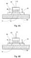
- FIG. 8APreparing a Semiconductor Substrate
- the fabrication processstarts with a substrate (silicon wafer substrate, glass substrate, compound Semiconductor substrate, or any suitable substrate), preferably a silicon substrate.
- a thin dielectric layeris deposited on the substrate to provide device isolation.
- the dielectric layeris preferably a silicon dioxide, deposited either by thermal oxidation process or a deposition process (sputtering process or chemical vapor deposition process such as plasma enhanced chemical vapor deposition process, or low pressure chemical vapor deposition process).
- the thickness of the dielectric layeris preferably between 50 nm to 200 nm. If a dielectric substrate (such as a glass substrate) is used, this dielectric layer might not be needed since the substrate already provides the needed device isolation.
- a thin layer of semiconductive metal oxidesuch as In 2 O 3 or RuO 2 is deposited onto the dielectric layer.
- the thickness of the semiconductive metal oxideis preferably between 20 nm to 100 nm.
- the semiconductive metal oxide layeris preferably properly doped with suitable impurities to achieve the right dopant and dopant concentration.
- the semiconductive metal oxide layeris then patterned to form active device areas.
- the patterning processis preferably photolithography process in which a photoresist mask is used to etch the semiconductive metal oxide layer, leaving islands for active device fabrication.
- FIG. 8Ashows a substrate 210 and a dielectric layer 216 , together with an active device area 214 of semiconductive metal oxide material. For simplicity, important but unrelated details is not shown, such as periphery devices and active region threshold voltage adjustment.
- FIG. 8BForming a Gate Stack on the Substrate
- the gate stack multilayer of ferroelectric film/top electrodeis deposited.
- a bottom electrode and/or a gate dielectriccan be added, and the gate stack multilayer can comprise three or four layers of optional gate dielectric, optional bottom electrode, ferroelectric film, and top electrode.
- the gate dielectricis preferably between 3 to 50 nm thick and is preferably silicon oxide, silicon nitride or any dielectric materials such hafnium oxide, aluminum oxide.
- the ferroelectric layeris preferably between 50 to 300 nm thick and is preferably PGO, PZT, STO, BST, BSTO, SBT, SBTN, PLT or PLZT, but can be any ferroelectric material exhibiting hysteresis effect.
- the top and bottom electrodeis preferably between 50 to 200 nm thick and is preferably aluminum, platinum or iridium, but also can be any conductive metal or conductive oxide materials. Furthermore, the electrode layers (either the bottom or the top electrode) can be a multilayer of metal and conductive oxide.
- the gate stack multilayeris then patterned into a ferroelectric gate stack, for example a top electrode 213 and a ferroelectric 212 as shown in FIG. 8B .
- the patterning of the gate stack multilayeris preferably by photolithography where a patterned mask is provided on the gate stack multilayer, then the gate stack multilayer is etched according to the pattern mask, and then the patterned mask is removed.
- the patterned maskis preferably a photoresist layer, coated and exposed to UV light under a photo mask to transfer a pattern from the photo mask onto the photoresist.
- the photoresist maskprotects the gate stack multilayer during an etch step to transfer the pattern from the photoresist onto the gate stack multilayer. And then the photoresist mask can be stripped.
- the gate stack multilayer etchingis preferably accomplished by reactive ion etching or by wet etches.
- the next stepis low doping drain (LDD) ion implantation into source 218 and drain 219 regions, although the ferroelectric memory transistor may or may not requires this LDD ion implantation.
- the next stepis sidewall spacer formation.
- a layer of dielectric materialsuch as silicon nitride, silicon dioxide or aluminum oxide is deposited onto the gate stack to a thickness of about between 20 to 80 nm, and then is anisotropic etched to leave a dielectric sidewall spacer 220 on the ferroelectric gate stack ( FIG. 8D ).
- the sidewall spacercan be used to protect the ferroelectric material from property degradation such as hydrogen diffusion.
- FIG. 8EForming Drain and Source Regions on Opposite Sides of the Gate Stack, FIG. 8E .
- a source region 221 and a drain region 222are formed by implantation of doping ions ( FIG. 8E ).
- the device fabrication processis then completed with passivation and interconnect metallization steps, FIG. 8F .
- a passivation layer 235such as silicon dioxide is deposited on the whole structure to a thickness of about 1000 to 2000 nm.
- the passivation layermay be planarized to improve the topology of the substrate.
- the structureis then annealed at a temperature of between about 400° C. to 500° C. for about 15 to 60 minutes.
- the passivation layeris then patterned, preferably by photolithography, to form contact holes, and then the fabrication process continued with first level metallization contact 241 to source 221 , contact 243 to gate stack (top electrode 213 , and ferroelectric 212 ), contact 242 to drain 222 .
- the gate etching process for the alternative embodiments of the present inventionis similar to the above gate etching process, with the addition of the bottom gate electrode and gate dielectric steps.
- the ferroelectric gate stackmay be fabricated by a replacement gate process similar to Hsu et al., U.S. Pat. No. 6,274,421, entitled “Method of making metal gate sub-micron MOS transistor”, hereby incorporated by reference.
- the fabrication processuses a replacement process to form the gate stack and comprises the steps of:
- the device fabrication processis then completed with passivation and interconnect metallization steps.
- FIG. 9APreparing a Semiconductor Substrate
- the fabrication processstarts with preparing a substrate (silicon wafer substrate, glass substrate, compound semiconductor substrate, or any suitable substrate), preferably a silicon substrate.
- a thin dielectric layeris deposited on the substrate to provide device isolation.
- the dielectric layeris preferably a silicon dioxide either by thermal oxidation process or a deposition process (sputtering process or chemical vapor deposition process such as plasma enhanced chemical vapor deposition process, low pressure chemical vapor deposition process).
- the thickness of the dielectric layeris preferably between 50 nm to 200 nm. If a dielectric substrate (such as a glass substrate) is used, the dielectric layer might not be needed.
- a thin layer of semiconductive metal oxidesuch as In 2 O 3 or RuO 2 is deposited onto the dielectric layer.
- the thickness of the semiconductive metal oxideis preferably between 20 nm to 100 nm.
- the semiconductive metal oxide layeris then patterned to form active device areas.
- the patterning processis preferably photolithography process in which a photoresist mask is used to etch the semiconductive metal oxide layer, leaving islands for active device fabrication.
- FIG. 9Ashows a substrate 310 and a dielectric layer 316 , together with an active device area 314 of semiconductive metal oxide material. For simplicity, important but unrelated details is not shown, such as periphery devices, possible well formation process and active region threshold voltage adjustment.
- FIG. 9BForming a Replacement Gate Stack Comprising a Sacrificial Layer on the Substrate
- the multilayer replacement gate stackserves as a place holder for the continued fabrication of the device, and will be removed before the fabrication of the functional gate stack.
- the multilayer replacement gate stackcomprises a sacrificial gate replacement layer.
- the replacement gate stackcomprises also a bottom electrode or a gate dielectric of the multilayer gate stack.
- the sacrificial gate replacement layeris preferably between about 50 to 200 nm thick and is preferably silicon nitride or silicon dioxide. Since the sacrificial gate replacement layer serves as a place holder for the functional gate stack, the thickness of the sacrificial layer is partially determined by the total thickness of the remainder of the functional gate stack.
- the replacement gate stack multilayeris then patterned into a ferroelectric gate stack, comprising a replacement gate layer 330 as shown in FIG. 9B .
- the patterning of the gate stack multilayeris preferably by photolithography and reactive ion etching.
- the next stepis optional low doping drain (LDD) ion implantation, and possible sidewall spacer formation, although the ferroelectric memory transistor may or may not requires this LDD ion implantation.
- LDDlow doping drain
- FIG. 9CForming drain and source regions on opposite sides of the replacement gate stack, ( FIG. 9C ):
- a source region 321 and a drain region 322are formed by implantation of doping ions.
- Contacts for the source and drain regionscan be fabricated with a thin layer of metal 350 such as Pt, Ir, Ti, TiN, TaN, or a multilayer of these metal materials.
- the metal layeris preferably deposited by a directional technique such as sputtering process. The sputtering process deposits a uniform layer of metal on the flat surface with little or even no metal being deposited onto the vertical sidewall of the silicon nitride sacrificial gate. Photolithography using photoresist mask can be used to etch metal from the non-active area ( FIG. 9D ).
- FIG. 9E
- a dielectric layer 335 such as silicon dioxideis deposited on the whole structure.
- the dielectric layeris then planarized, preferably by a chemical mechanical polishing (CMP) process.
- the thickness of the dielectric layeris preferably about 50% thicker than the replacement gate layer 330 and the semiconductive metal oxide, 314 to prevent dishing during planarization.
- the CMP processstops at the metal layer 350 on the silicon nitride sacrificial gate, and the metal on the sacrificial gate may or may not be completely removed ( FIG. 9E ).
- FIG. 9FRemoving the Sacrificial Layer Portion of the Replacement Gate Stack
- the replacement gate layer 330 and the remaining metal layer 350are removed to expose a gate trench 337 , preferably by a selective wet etch process to prevent damage to the surrounding structure.
- the metal at the sidewall of the gate trenchis removed also with a wet etch process.
- a spacer 340is fabricated in the sidewall of the gate trench to protect the ferroelectric gate stack.
- the spacer formationis preferably by depositing a layer of silicon nitride or aluminum oxide of about 5 to 20 nm thick, and then anisotropically etched by plasma reactive ion etching ( FIG. 9F ).
- FIG. 9HForming the Remainder of the Gate Stack
- the ferroelectric layeris then deposited into the gate trench.
- the ferroelectric layeris perferably PGO, PZT, STO, BST, BSTO, SBT, SBTN, PLT or PLZT, but can be any ferroelectric material exhibiting hysteresis effect.
- the thickness of the ferroelectric layeris preferably slightly thicker than the depth of the gate trench to minimize the dishing effect during the subsequent CMP process of planarize the ferroelectric layer 312 ( FIG. 9G ).
- the top electrodeis then fabricated on the ferroelectric layer 312 .
- the top electrode formationis preferably by depositing a blanket layer of top electrode material, and then is patterned into the top electrode, preferably by photolithography and reactive ion etching techniques.
- the top electrodeis preferably between 50 to 200 nm thick and is preferably aluminum, platinum or iridium, but also can be any conductive materials ( FIG. 9H ).
- a passivation layersuch as silicon dioxide is deposited on the whole structure to a thickness of about 300 to 500 nm.
- the structureis then annealed at a temperature of between about 400° C. to 500° C. for about 15 to 60 minutes.
- the passivation layeris then patterned, preferably by photolithography, to form contact holes, and then the fabrication process continued with first level metallization contact 341 to source 321 , contact 343 to gate stack (top electrode 313 , ferroelectric 312 , bottom electrode 311 and conductive oxide 301 ), contact 342 to drain 322 .
- a CMP planarization stepmay be added to have a planar surface.
- the above stepscan be repeated for more level memory transistor fabrication to form 3D memory structure ( FIG. 9J ).
- the replacement gate process for the alternative embodiments of the present inventionis similar to the above replacement process, with the exception of the addition of the bottom gate electrode or the gate dielectric steps.
Landscapes
- Semiconductor Memories (AREA)
- Non-Volatile Memory (AREA)
- Thin Film Transistor (AREA)
Abstract
Description
- This invention related generally to semiconductor device and nonvolatile memory transistor, and more particularly to ferroelectric gate transistor structures and methods of fabrication.
- Ferroelectric materials are composed of many randomly-distributed permanently polarized regions. Under the presence of an electric field, the regions with a polarization component in the direction of the electric field grow at the expense of the non-aligned regions so that a net polarization can result. If the electric field decreases, the polarization also decreases but at a slower rate so that even when the electric field becomes zero, a remnant polarization remains. This remnant polarization, existed under zero field condition (i.e., when power is turned off), is the basis of ferroelectric nonvolatile memory devices such as ferroelectric transistors.
- The ferroelectric transistor is typically a ferroelectric-gate-controlled semiconductor field-effect transistor (FET), which employs a ferroelectric film in contact with a silicon substrate, and in which a proper polarization of the ferroelectric film can create an inversion layer in the silicon channel of the transistor. The basic ferroelectric-gate controlled field-effect transistor is a metal-ferroelectric silicon (MFS) FET. The term MFS represents the layers in the gate stack of the ferroelectric transistor, consisting a metal (M) gate electrode disposed on a ferroelectric (F) gate dielectric on the silicon (S) channel of the transistor.
- However, effective transistor operation of the above MFS transistor is difficult to achieve due to the requirement of the ferroelectric/silicon interface. When a ferroelectric film is deposited directly on the silicon substrate, metals and oxygen from the ferroelectric layer may diffuse into the ferroelectric-silicon interface, creating interface trapped charges which affect the polarization of the ferroelectric film, and overall may make the operation of the ferroelectric transistor unstable. Further, since the thermal expansion coefficient and lattice structure of a ferroelectric film is not compatible with silicon, it is very difficult to form a high-quality ferroelectric film with a clean interface directly on the silicon substrate.
- Various designs have been proposed to address the drawbacks posed by the direct ferroelectric/silicon interface such as the addition of an interface layer such as a gate dielectric, a metal layer, a conductive metal oxide or a doped conductive metal oxide between the ferroelectric film and the silicon substrate.
- The gate dielectric interface design can overcome the surface interface and surface state issues of a ferroelectric layer in contact with the silicon substrate, but they incorporate other difficulties such as higher operation voltage and trapped charges in the bottom floating gate layer. The operation voltage of these transistors is higher than the ferroelectric layer programming voltage by an amount of the voltage across the gate dielectric. And when there is a voltage applied across the ferroelectric thin film, there will be current flow in the gate stack, and charges would be trapped in this floating electrode. The trapped charges may neutralize the polarization charges at the interface of the bottom electrode and the ferroelectric film and could shorten the memory retention time of this structure.
- The metal interface design is based on the formation of a Schottky diode in a metal-ferroelectric-metal silicon (MFMS) device. A Schottky barrier is formed between the bottom metal electrode of the gate unit (or a very shallow junction layer) and the silicon substrate. The Schottky ferroelectric gate memory transistor requires a space between the bottom electrode and the source and drain region and a very shallow n-channel under the gate, therefore the drive current of the Schottky ferroelectric gate memory transistor can be relatively low.
- Other novel ferroelectric transistor designs employ a conductive oxide, a conductive metal oxide or a doped conductive metal oxide interfacial layer between the ferroelectric material and the silicon substrate, as disclosed in co-pending application entitled “Conductive metal oxide gate ferroelectric memory transistor”, and “In2O3thin film resistivity control by doping metal oxide insulator for MFMox device applications” of the same first inventors, hereby incorporated by reference. A conductive oxide interface layer does not have the drawbacks of a dielectric interface layer, and may not have the drawbacks of the metal interface layer of a Schottky diode formation. The conductive oxide interfacial layer may improve the quality of the ferroelectric film and the operation of the ferroelectric transistor by possible lattice matching with the ferroelectric layer, reducing or eliminating the oxygen diffusion problem at the ferroelectric interface to improve the reliability of the ferroelectric transistor, and possible etch selectivity improving with other dielectric and metal films.
- Despite the obvious advantages of the conductive oxide, prior art ferroelectric transistor designs all employ a silicon conduction channel, leading to relatively complicated device fabrication process, together with the difficulty in 3D integration.
- Under appropriate conditions, certain conductive metal oxide materials behave as a semiconductor, and therefore the present invention discloses a novel transistor structure employing semiconductive metal oxide as the transistor conductive channel. By replacing the silicon conductive channel with a semiconductive metal oxide channel, the transistors can achieve simpler fabrication process and could realize 3D structure to increase circuit density.
- The disclosed semiconductive metal oxide transistor can have great potential in ferroelectric non volatile memory device. Besides the simpler fabrication process and possible 3D structure for higher memory density, the present invention ferroelectric semiconductive metal oxide transistor can provide good interfacial properties with the ferroelectric materials, possibly improving the ferroelectric film quality and reducing floating gate effect by omitting the gate dielectric. The semiconductive metal oxide further can have the advantages of possible lattice matching with the ferroelectric layer, reducing or eliminating the oxygen diffusion problem at the ferroelectric interface to improve the reliability of the ferroelectric transistor, and possible etch selectivity improvement with other dielectric and metal films.
- The semiconductive metal oxide film is preferably a metal oxide exhibiting semiconducting properties at the transistor operating conditions, for example, In2O3or RuO2. The semiconductive metal oxide film can also be doped with n or p type impurity species to modify the conductivity. By varying the dopant concentration and other fabrication process parameters, the semiconductive metal oxide film can achieve the proper properties such as the ability to change resistance as a function of applied field suitable for the operation and optimization of the ferroelectric transistor performance.
- The present invention ferroelectric transistor can be a metal-ferroelectric-semiconductive metal oxide FET. The gate stack of this transistor has a top metal electrode (or top gate) disposed on a ferroelectric layer disposed on a semiconductive metal oxide channel on a substrate. The present invention ferroelectric transistor can be a metal-ferroelectric-metal-semiconductive metal oxide FET. The gate stack of this transistor has a top metal electrode (or top gate) disposed on a ferroelectric layer disposed on a bottom metal electrode (or bottom gate) disposed on a semiconductive metal oxide channel on a substrate. The present invention ferroelectric transistor can also include a gate dielectric or a resistive oxide on the semiconductive metal oxide channel such as a metal-ferroelectric-gate dielectric-semiconductive metal oxide FET or a metal-ferroelectric-metal-gate dielectric-semiconductive metal oxide FET.
- The fabrication process of the present invention ferroelectric transistor can be performed by a gate etching process or by a replacement gate process. In the gate etching process, the multilayer gate stack is deposited and etched, while in the replacement gate process, a replacement gate stack is deposited as a place holder for the fabrication of other portions of the device, then the replacement gate stack is removed and the functional gate stack is deposited.
FIG. 1 shows a prior art ferroelectric-gate-controlled semiconductor field-effect transistor (FET) which is a metal-ferroelectric silicon (MFS) FET.FIG. 2A shows a schematic of a prior art metal-ferroelectric-oxide silicon MFOS transistor.FIG. 2B shows a schematic of a prior art metal-ferroelectric-metal-oxide silicon MFMOS transistor.FIG. 3 shows a schematic of the present invention semiconductive metal oxide ferroelectric transistor.- FIGS.4A-B shows the operation of the present invention semiconductive metal oxide ferroelectric transistor.
FIG. 5 shows another embodiment of the present invention semiconductive metal oxide ferroelectric transistor having a gate stack of top electrode/ferroelectric/bottom electrode disposed on a semiconductor metal oxide channel.FIG. 6 shows another embodiment of the present invention semiconductive metal oxide ferroelectric transistor having a gate stack of top electrode/ferroelectric/gate dielectric disposed on a semiconductor metal oxide channel.FIG. 7 shows another embodiment of the present invention semiconductive metal oxide ferroelectric transistor having a gate stack of top electrode/ferroelectric/bottom electrode/gate dielectric disposed on a semiconductor metal oxide channel.- FIGS.8A-F shows a representative fabrication process for gate etching process.
- FIGS.9A-J shows a representative fabrication process for replacement gate process.
- The present invention discloses a transistor structure having a semiconductive metal oxide substrate as the conductive channel. By replacing the silicon conductive channel with a semiconductive metal oxide channel, the transistor device can achieve simpler fabrication process and could realize 3D integration structure to increase circuit density. The transistor having a semiconductive metal oxide channel of the present invention is preferably employed as a ferroelectric non volatile memory field effect transistor.
- Metal oxide semiconductors have been used as gas sensing materials because of their high sensitivity to the presence of various gases in the ambient atmosphere. The typical gas sensor operates on the principle that the film resistance of a semiconductor metal oxide film changes significantly upon the chemical reaction between the gas species to be detected and the semiconductor metal oxide sensing film. The film resistance then becomes a direct measurement of the gas concentration. Semiconductor metal oxide gas sensor can be used to detect gases such as CO, alcohol and oxygen.
- The high sensitivity of the semiconductor metal oxides is due to their semiconducting properties since semiconductive metal oxides can be classified as poor semiconductors. The conductivity of these oxides can change significantly with the doping of n or p-type impurities and both doped and un-doped semiconducting metal oxides have been studied for gas sensor applications. Typical semiconductor metal oxides utilized in gas detection are molybdenum oxide (MoO3), which possesses excellent catalytic, electrochromic and gas sensing properties, tungsten oxide (WO3) which has been used to detect various gases due to its excellent semiconducting properties, and titanium oxide TiO2which is photoreactive and change conductivity upon irradiated with light of a given wavelength. Other semiconductor oxide materials suitable for sensor applications are tin oxide (SnO2), iron oxide (Fe2O3), indium oxide (In2O3), cesium oxide (CeO2), zinc oxide (ZnO2), gallium oxide (Ga2O3), SrTiO, LaFeO3, Cr1.8Ti0.2O3.
- The present invention discloses a transistor employing a semiconductive metal oxide channel, especially a ferroelectric memory transistor, to simplify the fabrication process and to improve the suitability for 3D integration. The ferroelectric transistor of the present invention is a ferroelectric field effect transistor having a semiconductive metal oxide conduction layer replacing the silicon conduction layer. The present invention semiconductive metal oxide transistor comprises a source and a drain regions provided in a semiconductive metal oxide film, and the ferroelectric transistor further comprises a ferroelectric gate structure between the source and drain regions.
FIG. 1 shows the schematic of a prior art n-channel metal-ferroelectric silicon MFS transistor. Aferroelectric film 12 is formed as a gate insulating film on a p-type silicon substrate 13, together withsource 14 and drain15 regions having a high concentration of n-type impurity ions. Ametal gate electrode 11 is formed over theferroelectric film 12. The MFS transistor is isolated by theisolation trenches 16. The basic drawback of the above ferroelectric transistor is the difficulty in fabricating a good ferroelectric/silicon interface.- To address the drawbacks posed by the direct ferroelectric/silicon interface, a gate dielectric can be inserted between the ferroelectric film and the silicon substrate. The ferroelectric transistor is then called metal-ferroelectric-oxide (or insulator) silicon (MFOS or MFIS) FET.
FIG. 2A shows a MFOS memory transistor using agate oxide layer 27 formed between thesilicon substrate 13 and theferroelectric film 12. Alternatively, a metal floatinggate layer 28 can be added between theferroelectric film 12 and thegate oxide layer 27 as shown inFIG. 2B for a metal-ferroelectric-metal-oxide (or insulator) silicon (MFMOS or MFMIS) transistor. A suitable conducting material (e.g. Pt or Ir) is normally selected for the floatinggate 28 to allow the deposition of the ferroelectric thin film and to prevent diffusion of the ferroelectric material into the gate dielectric and the channel. The floatinggate layer 28 is also called bottom electrode, or bottom gate, in reference to theother gate electrode 11, called top electrode, or top gate. The basic drawback for this ferroelectric transistor design is the possible floating gate effect, caused by the insulation of the gate dielectric. - Other interfacial layers can be employed to improve the ferroelectric/silicon interfacial problem such as the formation of a Schottky diode such as a metal-ferroelectric-metal silicon (MFMS) device disclosed in Nakao et al., U.S. Pat. No. 5,303,182, entitled “Nonvolatile semiconductor memory utilizing aferroelectricfilm”. A thin metal layer is position between the ferroelectric layer and the silicon substrate, and a Schottky barrier is formed between this metal layer and the silicon substrate. To prevent shortage between the gate and the source/drain regions, the Schottky ferroelectric gate memory transistor requires a space between the bottom electrode and the source and drain regions or a very shallow n-channel under the gate, therefore the drive current of the Schottky ferroelectric gate memory transistor can be relatively low. Hsu et al., U.S. Pat. No. 5,731,608, entittled “One transistor ferroelectric memory cell and method of making the same”, and its continuations and divisions (U.S. Pat. Nos. 5,962,884; 6,117,691; 6,018,171; 5,942,776; 5,932,904; 6,146,904; 6,011,285; 6,531,325), hereby incorporated by reference, disclose a distance between 50 to 300 nm from the bottom metal electrode to the source and drain to reduce the possible high leakage current due to the increased field intensity at the metal edge of the Schottky diode because of the sharp edge at the periphery of the metal contact. Alternatively, Willer et al., U.S. Pat. No. 6,538,273, entittled “Ferroelectric transistor and method for fabricating it”, discloses a recess of the source and drain below the surface of the semiconductor surface in a Schottky ferroelectric gate memory transistor.
- An interfacial layer of conductive metal oxide can be employed in a co-pending application entitled “Conductive metal oxide gate ferroelectric memory transistor” of the same first inventor, disclosing a ferroelectric transistor having a conductive oxide in the place of the gate dielectric. By replacing the gate dielectric with a conductive oxide, the bottom gate of the ferroelectric layer is conductive through the conductive oxide to the silicon substrate, therefore there is no floating gate effect. The memory retention degradation related to the leakage current associated with the charges trapped within the floating gate is eliminated. Furthermore, the operating voltage for the ferroelectric transistor can be reduced to the ferroelectric layer programming voltage because of the absence of the gate dielectric.
- Another co-pending application entitled “In2O3thin film resistivity control by doping metal oxide insulator for MFMox device applications” of the same first inventors, has also disclosed a novel interfacial layer design by the use of a resistive oxide film in place of the gate dielectric, fabricated with proper resistance value to optimize the performance of the ferroelectric transistor. By replacing the gate dielectric with a resistive oxide film, and by optimizing the value of the film resistance, the bottom gate of the ferroelectric layer is electrically connected to the silicon substrate, therefore the floating gate effect can be eliminated, resulting in the improvement of the memory retention characteristics. Furthermore, the operating voltage for the ferroelectric transistor can be reduced because of the absence of the gate dielectric.
- The disclosed conductive oxide is preferably a conductive metal oxide, but can be a conductive oxide without any metal components. The conductive oxide can make good interface with the silicon substrate, and can be selected to have a good lattice matching with the deposited ferroelectric film, especially ones having perovskite crystal structures.
- Furthermore, a conductive oxide serving as electrodes for the ferroelectric film may improve the quality of the ferroelectric film, and thus the operation of the ferroelectric transistor. A ferroelectric film is generally formed in an oxidizing ambience such as a deposition process with oxygen as a reactive gas, or an annealing process in an oxygen ambience to improve the stability of the deposited ferroelectric film. Therefore the electrode material for a ferroelectric film is preferable an oxidization resistant noble metal such as Pt and Ir. Conductive oxides is already oxidation resistant, and further, due to the high concentration of oxygen, the conductive oxide film can suppress the movement and accumulation of oxygen at the ferroelectric/conductive oxide interface to improve the reliability such as fatigue and the controllability of the ferroelectric and therefore its polarization property.
- One further advantage of conductive metal oxide is the etch selectivity. Oxygen can be used as an etching gas for conductive metal oxides since a steam pressure of metal oxide is typically very high. The conductive metal oxide therefore can be etched with high selective etching rate to other dielectric films. In addition, the conductive metal oxide and the metal can have high selective etching rate since the conductive metal oxide films (RuO2, for example) normally cannot easily react with halogen such as F and Cl used for etching the metal films.
- Under proper conditions, the conductive metal oxide disclosed above can behave as a semiconductor as utilized extensively in various gas sensor applications. The present invention thus discloses a semiconductor metal oxide ferroelectric memory transistor, taking the advantages of a good interface between a semiconductive metal oxide and a ferroelectric layer. Further, by using a semiconductive metal oxide material as the device channel, the present invention transistor can be fabricated either horizontally or vertically planar, as well as able to stack many layers of devices in a 3D structure.
- The first embodiment of the present invention is shown in
FIG. 3 , illustrating a semiconductive metal oxide ferroelectric transistor. The gate stack of the present invention comprises atop gate electrode 63 and aferroelectric film 62, positioning on a semiconductivemetal oxide layer 51 disposed on asubstrate 69, and disposed between thesource 64 and drain65 regions having a high concentration of opposite type impurity ions. The ferroelectric transistor is isolated by theisolation substrate 69. The conductive channel layer of the present invention transistor is fabricated with a semiconductive metal oxide such as In2O3 or RuO2. The semiconductive metal oxide in this example can be doped with p-type (n-type) impurities to form n-type (p-type) semiconductive metal oxide material. FIG. 4 show the operation of an n-channel semiconductive metal oxide ferroelectric transistor. InFIG. 4A , when a positive voltage is applied to thegate electrode 63, polarization of theferroelectric film 62 occurs with electrons are pulled to the top and holes are pulled to the bottom of the ferroelectric film. Electrons are then accumulated at the bottom electrode and the surface of the silicon under the ferroelectric gate stack. This forms a highconductive channel 67. Therefore the ferroelectric transistor is “ON”, i.e. if a voltage bias is placed across thesource 64 and thedrain 65, a current will flow through the transistor. The ferroelectric transistor memory is nonvolatile, meaning that the transistor remains in the ON state even after this positive voltage is removed due to the remnant polarization of theferroelectric film 62.- In
FIG. 4B , when a negative voltage is applied to thegate electrode 63, opposite polarization occurs in theferroelectric film 62 with holes are pulled to the top of the ferroelectric gate and electrons are pulled to the bottom of the ferroelectric film. Holes then are accumulated at the bottom electrode and the surface of the silicon under the ferroelectric gate stack. There are noconduction channel 67, and the ferroelectric transistor is “OFF”, i.e. a non-conduction state takes place between thesource 64 and drain65 regions, which is maintained even after the negative voltage is removed. - In the second embodiment of the invention, a bottom gate electrode is included. Thus gate stack of the semiconductive metal oxide gate ferroelectric transistor comprises a
top gate electrode 163, aferroelectric film 162 and abottom gate electrode 61 as shown inFIG. 5 . Thebottom electrode 61 is connected to the semiconductivemetal oxide channel 51, and therefore thebottom electrode 61 is not electrically isolated, and would not be able to accumulate charges likes a floating gate. The charge retention time of this device is thus independent of the current flow through the ferroelectric thin film. - In alternate embodiments of the invention, a gate dielectric is included. Thus gate stack of the semiconductive metal oxide gate ferroelectric transistor comprises a
top gate electrode 163, aferroelectric film 162 and agate dielectric 81 as shown inFIG. 6 , or atop gate electrode 163, aferroelectric film 162, abottom electrode 61 and agate dielectric 81 as shown inFIG. 7 . The gate dielectric can also be a resistive material as disclosed in a co-pending application entitled “In2O3thin film resistivity control by doping metal oxide insulator for MFMox device applications”. - The semiconductive metal oxide in the present invention is preferably a metal oxide exhibiting semiconducting properties, such as indium oxide (In2O3), ruthenium oxide (RuO2), tungsten oxide (WO3), molybdenum oxide (MoO3), titanium oxide (TiO2), tin oxide (SnO2), iron oxide (Fe2O3), cesium oxide (CeO2), zinc oxide (ZnO2), gallium oxide (Ga2O3), SrTiO, LaFeO3, Cr1.8Ti0.2O3.
- The semiconductive metal oxide film can also be an oxide film of any one metal selected from a group of Mo, W, Tc, Re, Ru, Os, Rh, Ir, Pd, Pt, In, Zn, Sn, Sr—Ru or Sr—Co (such as IrO2and RuO2), or a rock-salt (NaCl) crystal structure face-centered cubic metal oxide, such as NdO, NbO, SmO, LaO, and VO. The preferred method of forming the semiconductive metal oxide is by deposition. However, other methods may be used such as doping by diffusion and ion implantation. For example, the semiconductive metal oxide can be boron (B) doped or fluorine (F) doped ZnO and antimony (Sb) doped or fluorine (F) doped SnO2.
- The semiconductive metal oxide may be composed of any number of conductive perovskite oxides such as lanthanum strontium cobalt oxide (LSCO). Typical examples of simple perovskite oxides are expressed by the general formula ABO3such as SrRuO3or LaNiO3, where AB can be any combination of (A=Ca, Sr)(B═V, Cr, Fe, Ru), (A=La)(B═Ti, Co, Ni, Cu), (A═H, Li, Na, K)(B═Re, Mo, Nb), (A=La1−xSrx)(B═V, Mn, Co). Another example of conductive perovskite oxides is expressed by the general formula A2B2O7where (A=Bi, Pd)(B═Ru1−xBix, Ru1−xPbx). Examples of layered perovskite oxides include CaTiO, (Sr(Ru, Ir, Cr)O3)(SrO)nsuch as SrRuO3, SrIrO3, Sr2RuO4, Sr2IrO4and Ba2RuO4. The semiconductive metal oxide film can also include high temperature superconducting oxides such as La1−xSrxCuO4, Nd1−xCexCuO4, YBa2Cu3O7, Bi2Sr2Can−1CunO2n+4, (Nd1−xCex)2CuO4. See, for example, Suzuki, U.S. Pat. No. 6,151,240, entitled “Ferroelectric nonvolatile memory and oxide multi-layered structure”, hereby incorporated by reference.
- The ferroelectric material disclosed in the present invention is preferably any of the following: Pb(Zr, Ti)O3(PZT), SrBi2Ta2O9(SBT), Pb5Ge3O11(PGO), BaTiO3, LiNbO3, STO, BST, BSTO, SBTN, PLT or PLZT, but any ferroelectric material exhibiting hysteresis effect can be employed in the conductive oxide ferroelectric transistor. The preferred ferroelectric compounds are, in order of preference, PGO, SBT and PZT. The ferroelectric layer is preferably capped with a passivation layer such as silicon nitride (Si3N4) or aluminum oxide (Al2O3) to prevent hydrogen reaction.
- The bottom electrode and the top electrode are preferably a metal layer such as aluminum, platinum or iridium, and more preferably a conductive layer, a conductive oxide layer, a conductive metal oxide layer, or a multilayer such as conductive oxide/metal, or conductive metal oxide/metal.
- Within the scope of the invention, the disclosed semiconductive metal oxide ferroelectric transistor structure may also incorporate all the advanced features of the state of the art technology such as SOI or SIMOX substrate, halo or LDD source and drain, sidewall spacers for the gate stack, shallow trench isolation (STI) or LOCOS isolation, silicide formation such as titanium silicide, cobalt silicide, or nickel silicide, raised source and drain, passivation, tungsten or aluminum contact, aluminum or copper metallization.
- The present invention further discloses the fabrication process for the semiconductive metal oxide ferroelectric transistor. Although the fabrication process for the semiconductive metal oxide ferroelectric transistor is illustrated and described below with reference to certain specific processes, the present invention is nevertheless not intended to be limited to the details shown. The general process of semiconductor fabrication has been practiced for many years, and due to the multitude of different ways of fabricating a device or structure, various modifications may be made in the fabrication process details within the scope and range of the present invention and without departing from the meaning of the invention.
- One fabrication process for the semiconductive metal oxide ferroelectric transistor is a gate etching process, employing an etching process to form the gate stack and comprising the steps of:
- Preparing a semiconductor metal oxide channel layer
- Forming a gate stack on the semiconductor metal oxide layer
- Forming drain and source regions on opposite sides of the gate stack in the semiconductor metal oxide.
- The device fabrication process is then completed with passivation and interconnect metallization steps. After passivation, another device can also fabricated on top of the previous device to form 3D memory structure.
- Preparing a Semiconductor Substrate,
FIG. 8A : - The fabrication process starts with a substrate (silicon wafer substrate, glass substrate, compound Semiconductor substrate, or any suitable substrate), preferably a silicon substrate. A thin dielectric layer is deposited on the substrate to provide device isolation. The dielectric layer is preferably a silicon dioxide, deposited either by thermal oxidation process or a deposition process (sputtering process or chemical vapor deposition process such as plasma enhanced chemical vapor deposition process, or low pressure chemical vapor deposition process). The thickness of the dielectric layer is preferably between 50 nm to 200 nm. If a dielectric substrate (such as a glass substrate) is used, this dielectric layer might not be needed since the substrate already provides the needed device isolation. Then a thin layer of semiconductive metal oxide such as In2O3or RuO2is deposited onto the dielectric layer. The thickness of the semiconductive metal oxide is preferably between 20 nm to 100 nm. The semiconductive metal oxide layer is preferably properly doped with suitable impurities to achieve the right dopant and dopant concentration. The semiconductive metal oxide layer is then patterned to form active device areas. The patterning process is preferably photolithography process in which a photoresist mask is used to etch the semiconductive metal oxide layer, leaving islands for active device fabrication.
FIG. 8A shows asubstrate 210 and adielectric layer 216, together with anactive device area 214 of semiconductive metal oxide material. For simplicity, important but unrelated details is not shown, such as periphery devices and active region threshold voltage adjustment.- Forming a Gate Stack on the Substrate,
FIG. 8B : - Then the gate stack multilayer of ferroelectric film/top electrode is deposited. In alternate embodiments of the invention, a bottom electrode and/or a gate dielectric can be added, and the gate stack multilayer can comprise three or four layers of optional gate dielectric, optional bottom electrode, ferroelectric film, and top electrode. The gate dielectric is preferably between 3 to 50 nm thick and is preferably silicon oxide, silicon nitride or any dielectric materials such hafnium oxide, aluminum oxide. The ferroelectric layer is preferably between 50 to 300 nm thick and is preferably PGO, PZT, STO, BST, BSTO, SBT, SBTN, PLT or PLZT, but can be any ferroelectric material exhibiting hysteresis effect. The top and bottom electrode is preferably between 50 to 200 nm thick and is preferably aluminum, platinum or iridium, but also can be any conductive metal or conductive oxide materials. Furthermore, the electrode layers (either the bottom or the top electrode) can be a multilayer of metal and conductive oxide.
- The gate stack multilayer is then patterned into a ferroelectric gate stack, for example a
top electrode 213 and a ferroelectric212 as shown inFIG. 8B . The patterning of the gate stack multilayer is preferably by photolithography where a patterned mask is provided on the gate stack multilayer, then the gate stack multilayer is etched according to the pattern mask, and then the patterned mask is removed. The patterned mask is preferably a photoresist layer, coated and exposed to UV light under a photo mask to transfer a pattern from the photo mask onto the photoresist. The photoresist mask protects the gate stack multilayer during an etch step to transfer the pattern from the photoresist onto the gate stack multilayer. And then the photoresist mask can be stripped. The gate stack multilayer etching is preferably accomplished by reactive ion etching or by wet etches. - The next step is low doping drain (LDD) ion implantation into
source 218 and drain219 regions, although the ferroelectric memory transistor may or may not requires this LDD ion implantation. The next step is sidewall spacer formation. A layer of dielectric material such as silicon nitride, silicon dioxide or aluminum oxide is deposited onto the gate stack to a thickness of about between 20 to 80 nm, and then is anisotropic etched to leave adielectric sidewall spacer 220 on the ferroelectric gate stack (FIG. 8D ). The sidewall spacer can be used to protect the ferroelectric material from property degradation such as hydrogen diffusion. - Forming Drain and Source Regions on Opposite Sides of the Gate Stack,
FIG. 8E . - Then a
source region 221 and adrain region 222 are formed by implantation of doping ions (FIG. 8E ). The device fabrication process is then completed with passivation and interconnect metallization steps,FIG. 8F . Apassivation layer 235 such as silicon dioxide is deposited on the whole structure to a thickness of about 1000 to 2000 nm. The passivation layer may be planarized to improve the topology of the substrate. The structure is then annealed at a temperature of between about 400° C. to 500° C. for about 15 to 60 minutes. The passivation layer is then patterned, preferably by photolithography, to form contact holes, and then the fabrication process continued with firstlevel metallization contact 241 tosource 221, contact243 to gate stack (top electrode 213, and ferroelectric212), contact242 to drain222. - The gate etching process for the alternative embodiments of the present invention (the ferroelectric transistor with the gate stack of bottom electrode and/or gate dielectric) is similar to the above gate etching process, with the addition of the bottom gate electrode and gate dielectric steps.
- Alternatively, the ferroelectric gate stack may be fabricated by a replacement gate process similar to Hsu et al., U.S. Pat. No. 6,274,421, entitled “Method of making metal gate sub-micron MOS transistor”, hereby incorporated by reference. The fabrication process uses a replacement process to form the gate stack and comprises the steps of:
- Preparing a semiconductor substrate
- Forming a replacement gate stack comprising a sacrificial layer
- Forming drain and source regions on opposite sides of the replacement gate stack
- Filling the areas surrounding the replacement gate stack while exposing a top portion of the replacement gate stack
- Removing the sacrificial layer portion of the replacement gate stack
- Forming the remainder of the gate stack.
- The device fabrication process is then completed with passivation and interconnect metallization steps.
- Preparing a Semiconductor Substrate,
FIG. 9A : - Similar to the gate etching process, the fabrication process starts with preparing a substrate (silicon wafer substrate, glass substrate, compound semiconductor substrate, or any suitable substrate), preferably a silicon substrate. A thin dielectric layer is deposited on the substrate to provide device isolation. The dielectric layer is preferably a silicon dioxide either by thermal oxidation process or a deposition process (sputtering process or chemical vapor deposition process such as plasma enhanced chemical vapor deposition process, low pressure chemical vapor deposition process). The thickness of the dielectric layer is preferably between 50 nm to 200 nm. If a dielectric substrate (such as a glass substrate) is used, the dielectric layer might not be needed. Then a thin layer of semiconductive metal oxide such as In2O3or RuO2is deposited onto the dielectric layer. The thickness of the semiconductive metal oxide is preferably between 20 nm to 100 nm. The semiconductive metal oxide layer is then patterned to form active device areas. The patterning process is preferably photolithography process in which a photoresist mask is used to etch the semiconductive metal oxide layer, leaving islands for active device fabrication.
FIG. 9A shows asubstrate 310 and adielectric layer 316, together with anactive device area 314 of semiconductive metal oxide material. For simplicity, important but unrelated details is not shown, such as periphery devices, possible well formation process and active region threshold voltage adjustment.- Forming a Replacement Gate Stack Comprising a Sacrificial Layer on the Substrate,
FIG. 9B : - Then the multilayer replacement gate stack is deposited. The replacement gate stack serves as a place holder for the continued fabrication of the device, and will be removed before the fabrication of the functional gate stack. Thus the multilayer replacement gate stack comprises a sacrificial gate replacement layer. In other embodiments of the invention where a bottom electrode or a gate dielectric of the gate stack is included, the replacement gate stack comprises also a bottom electrode or a gate dielectric of the multilayer gate stack. The sacrificial gate replacement layer is preferably between about 50 to 200 nm thick and is preferably silicon nitride or silicon dioxide. Since the sacrificial gate replacement layer serves as a place holder for the functional gate stack, the thickness of the sacrificial layer is partially determined by the total thickness of the remainder of the functional gate stack.
- The replacement gate stack multilayer is then patterned into a ferroelectric gate stack, comprising a
replacement gate layer 330 as shown inFIG. 9B . The patterning of the gate stack multilayer is preferably by photolithography and reactive ion etching. - The next step is optional low doping drain (LDD) ion implantation, and possible sidewall spacer formation, although the ferroelectric memory transistor may or may not requires this LDD ion implantation.
- Forming drain and source regions on opposite sides of the replacement gate stack, (
FIG. 9C ): - Then a
source region 321 and adrain region 322 are formed by implantation of doping ions. Contacts for the source and drain regions can be fabricated with a thin layer ofmetal 350 such as Pt, Ir, Ti, TiN, TaN, or a multilayer of these metal materials. The metal layer is preferably deposited by a directional technique such as sputtering process. The sputtering process deposits a uniform layer of metal on the flat surface with little or even no metal being deposited onto the vertical sidewall of the silicon nitride sacrificial gate. Photolithography using photoresist mask can be used to etch metal from the non-active area (FIG. 9D ). - Filling the Areas Surrounding the Replacement Gate Stack While Exposing a Top Portion of the Replacement Gate Stack,
FIG. 9E : - A dielectric layer335 such as silicon dioxide is deposited on the whole structure. The dielectric layer is then planarized, preferably by a chemical mechanical polishing (CMP) process. The thickness of the dielectric layer is preferably about 50% thicker than the
replacement gate layer 330 and the semiconductive metal oxide,314 to prevent dishing during planarization. The CMP process stops at themetal layer 350 on the silicon nitride sacrificial gate, and the metal on the sacrificial gate may or may not be completely removed (FIG. 9E ). - Removing the Sacrificial Layer Portion of the Replacement Gate Stack,
FIG. 9F : - The
replacement gate layer 330 and the remainingmetal layer 350 are removed to expose agate trench 337, preferably by a selective wet etch process to prevent damage to the surrounding structure. The metal at the sidewall of the gate trench is removed also with a wet etch process. - A
spacer 340 is fabricated in the sidewall of the gate trench to protect the ferroelectric gate stack. The spacer formation is preferably by depositing a layer of silicon nitride or aluminum oxide of about 5 to 20 nm thick, and then anisotropically etched by plasma reactive ion etching (FIG. 9F ). - Forming the Remainder of the Gate Stack,
FIG. 9H : - The ferroelectric layer is then deposited into the gate trench. The ferroelectric layer is perferably PGO, PZT, STO, BST, BSTO, SBT, SBTN, PLT or PLZT, but can be any ferroelectric material exhibiting hysteresis effect. The thickness of the ferroelectric layer is preferably slightly thicker than the depth of the gate trench to minimize the dishing effect during the subsequent CMP process of planarize the ferroelectric layer312 (
FIG. 9G ). - The top electrode is then fabricated on the
ferroelectric layer 312. The top electrode formation is preferably by depositing a blanket layer of top electrode material, and then is patterned into the top electrode, preferably by photolithography and reactive ion etching techniques. The top electrode is preferably between 50 to 200 nm thick and is preferably aluminum, platinum or iridium, but also can be any conductive materials (FIG. 9H ). - The device fabrication process is then completed with passivation and interconnect metallization steps,
FIG. 9I . A passivation layer such as silicon dioxide is deposited on the whole structure to a thickness of about 300 to 500 nm. The structure is then annealed at a temperature of between about 400° C. to 500° C. for about 15 to 60 minutes. The passivation layer is then patterned, preferably by photolithography, to form contact holes, and then the fabrication process continued with firstlevel metallization contact 341 tosource 321, contact343 to gate stack (top electrode 313, ferroelectric312, bottom electrode311 and conductive oxide301), contact342 to drain322. - A CMP planarization step may be added to have a planar surface. The above steps can be repeated for more level memory transistor fabrication to form 3D memory structure (
FIG. 9J ). - The replacement gate process for the alternative embodiments of the present invention (the ferroelectric transistor with the gate stack of additional bottom electrode or gate dielectric) is similar to the above replacement process, with the exception of the addition of the bottom gate electrode or the gate dielectric steps.
- Thus a novel ferroelectric transistor and its memory cell application have been disclosed, together with the method of device fabrication. It will be appreciated that though preferred embodiments of the invention have been disclosed, further variations and modifications thereof may be made within the scope of the invention as defined in the appended claims. Further, although the invention has been described with reference to a ferroelectric transistor for use with nonvolatile memory applications, other applications of the inventive concepts disclosed herein will also be apparent to those skilled in the art.
Claims (43)
Priority Applications (2)
| Application Number | Priority Date | Filing Date | Title |
|---|---|---|---|
| US10/922,712US7378286B2 (en) | 2004-08-20 | 2004-08-20 | Semiconductive metal oxide thin film ferroelectric memory transistor |
| JP2005230168AJP2006060209A (en) | 2004-08-20 | 2005-08-08 | Semiconductive metal oxide thin film ferroelectric memory transistor |
Applications Claiming Priority (1)
| Application Number | Priority Date | Filing Date | Title |
|---|---|---|---|
| US10/922,712US7378286B2 (en) | 2004-08-20 | 2004-08-20 | Semiconductive metal oxide thin film ferroelectric memory transistor |
Publications (2)
| Publication Number | Publication Date |
|---|---|
| US20060038242A1true US20060038242A1 (en) | 2006-02-23 |
| US7378286B2 US7378286B2 (en) | 2008-05-27 |
Family
ID=35908858
Family Applications (1)
| Application Number | Title | Priority Date | Filing Date |
|---|---|---|---|
| US10/922,712Expired - Fee RelatedUS7378286B2 (en) | 2004-08-20 | 2004-08-20 | Semiconductive metal oxide thin film ferroelectric memory transistor |
Country Status (2)
| Country | Link |
|---|---|
| US (1) | US7378286B2 (en) |
| JP (1) | JP2006060209A (en) |
Cited By (71)
| Publication number | Priority date | Publication date | Assignee | Title |
|---|---|---|---|---|
| US20040240501A1 (en)* | 2003-05-30 | 2004-12-02 | Takashi Katoda | Photonic devices formed of high-purity molybdenum oxide |
| US20060157695A1 (en)* | 2005-01-19 | 2006-07-20 | Takashi Katoda | Electronic devices formed on substrates and their fabrication methods |
| US20060157696A1 (en)* | 2005-01-18 | 2006-07-20 | Takashi Katoda | Photonic devices formed on substrates and their fabrication methods |
| US20080001188A1 (en)* | 2006-06-30 | 2008-01-03 | Taiwan Semiconductor Manufacturing Co., Ltd. | SOI devices and methods for fabricating the same |
| US20080017936A1 (en)* | 2006-06-29 | 2008-01-24 | International Business Machines Corporation | Semiconductor device structures (gate stacks) with charge compositions |
| US7335594B1 (en)* | 2005-04-27 | 2008-02-26 | Spansion Llc | Method for manufacturing a memory device having a nanocrystal charge storage region |
| US7389675B1 (en)* | 2006-05-12 | 2008-06-24 | The United States Of America As Represented By The National Aeronautics And Space Administration | Miniaturized metal (metal alloy)/ PdOx/SiC hydrogen and hydrocarbon gas sensors |
| US20080203443A1 (en)* | 2007-02-22 | 2008-08-28 | American Semiconductor, Inc. | Independently-Double-Gated Transistor Memory (IDGM) |
| US20080258140A1 (en)* | 2007-04-20 | 2008-10-23 | Samsung Electronics Co., Ltd. | Thin film transistor including selectively crystallized channel layer and method of manufacturing the thin film transistor |
| US20080293208A1 (en)* | 2005-09-06 | 2008-11-27 | Canon Kabushiki Kaisha | Method of fabricating oxide semiconductor device |
| US20080315200A1 (en)* | 2007-06-19 | 2008-12-25 | Samsung Electronics Co., Ltd. | Oxide semiconductors and thin film transistors comprising the same |
| EP2120267A1 (en)* | 2008-05-15 | 2009-11-18 | Samsung Electronics Co., Ltd. | Semiconductor devices and methods of manufacturing the same |
| US20090294764A1 (en)* | 2008-05-29 | 2009-12-03 | Samsung Electronics Co., Ltd. | Oxide semiconductors and thin film transistors comprising the same |
| EP2159845A1 (en)* | 2008-09-01 | 2010-03-03 | Semiconductor Energy Laboratory Co, Ltd. | Oxide semiconductor device and method for manufacturing the same |
| EP2161756A1 (en)* | 2008-09-09 | 2010-03-10 | FUJIFILM Corporation | Thin film field-effect transistor and display using the same |
| US20110101343A1 (en)* | 2006-04-17 | 2011-05-05 | Chang-Jung Kim | ZnO based semiconductor devices and methods of manufacturing the same |
| US20110182102A1 (en)* | 2010-01-26 | 2011-07-28 | Kabushiki Kaisha Toshiba | Semiconductor memory device |
| US20110227064A1 (en)* | 2010-03-22 | 2011-09-22 | Samsung Electronics Co., Ltd. | Thin film transistors, methods of manufacturing thin film transistors, and semiconductor device including thin film transistors |
| US20120161126A1 (en)* | 2010-12-28 | 2012-06-28 | Semiconductor Energy Laboratory Co., Ltd. | Semiconductor device and manufacturing method thereof |
| US8268194B2 (en) | 2007-02-16 | 2012-09-18 | Samsung Electronics Co., Ltd. | Oxide semiconductor target |
| US20120248451A1 (en)* | 2009-12-25 | 2012-10-04 | Yuji Sone | Field-effect transistor, semiconductor memory display element, image display device, and system |
| US8450732B2 (en) | 2007-06-19 | 2013-05-28 | Samsung Electronics Co., Ltd. | Oxide semiconductors and thin film transistors comprising the same |
| KR20130058614A (en)* | 2011-11-25 | 2013-06-04 | 가부시키가이샤 한도오따이 에네루기 켄큐쇼 | Semiconductor device and method for manufacturing the same |
| US8716061B2 (en) | 2008-11-07 | 2014-05-06 | Semiconductor Energy Laboratory Co., Ltd. | Semiconductor device and method for manufacturing the same |
| WO2014071634A1 (en)* | 2012-11-12 | 2014-05-15 | 深圳市柔宇科技有限公司 | Self-aligned metal oxide thin film transistor device and manufacturing method |
| JP2014131052A (en)* | 2008-11-07 | 2014-07-10 | Semiconductor Energy Lab Co Ltd | Semiconductor device |
| US8829512B2 (en) | 2010-12-28 | 2014-09-09 | Semiconductor Energy Laboratory Co., Ltd. | Semiconductor device and method for manufacturing the same |
| US20160133753A1 (en)* | 2014-06-10 | 2016-05-12 | International Business Machines Corporation | Semiconductor devices containing an epitaxial perovskite/doped strontium titanate structure |
| JP2016146499A (en)* | 2010-08-06 | 2016-08-12 | 株式会社半導体エネルギー研究所 | Semiconductor device |
| EP2978012A4 (en)* | 2013-03-20 | 2016-10-19 | Boe Technology Group Co Ltd | THIN FILM TRANSISTOR AND ITS PREPARATION METHOD, MATRIX SUBSTRATE, AND DISPLAY DEVICE |
| US20170040181A1 (en)* | 2010-03-05 | 2017-02-09 | Semiconductor Energy Laboratory Co., Ltd. | Semiconductor device and manufacturing method thereof |
| US9722093B1 (en)* | 2016-06-30 | 2017-08-01 | United Microelectronics Corp. | Oxide semiconductor transistor and manufacturing method thereof |
| US20170263169A1 (en)* | 2009-01-22 | 2017-09-14 | Semiconductor Energy Laboratory Co., Ltd. | Method for driving display device |
| US20170317141A1 (en)* | 2016-04-28 | 2017-11-02 | HGST Netherlands B.V. | Nonvolatile schottky barrier memory transistor |
| US20170330967A1 (en)* | 2009-12-28 | 2017-11-16 | Sony Corporation | Semiconductor component and manufacturing method thereof |
| CN107359122A (en)* | 2017-06-07 | 2017-11-17 | 西安电子科技大学 | Mn adulterates the preparation method of hetero-junctions spin fet |
| CN107359127A (en)* | 2017-06-07 | 2017-11-17 | 西安电子科技大学 | The Fe doping spin fets and its manufacture method of Sapphire Substrate |
| CN107369707A (en)* | 2017-06-07 | 2017-11-21 | 西安电子科技大学 | Based on 4H SiC substrate hetero-junctions spin fets and its manufacture method |
| CN107658337A (en)* | 2017-06-07 | 2018-02-02 | 西安电子科技大学 | High electron mobility spin fet and preparation method thereof |
| US9911858B2 (en) | 2010-12-28 | 2018-03-06 | Semiconductor Energy Laboratory Co., Ltd. | Semiconductor device and method for manufacturing the same |
| WO2018125118A1 (en)* | 2016-12-29 | 2018-07-05 | Intel Corporation | Back-end ferroelectric field-effect transistor devices |
| US10056463B2 (en) | 2016-06-30 | 2018-08-21 | United Microelectronics Corp. | Transistor and manufacturing method thereof |
| WO2018236360A1 (en)* | 2017-06-20 | 2018-12-27 | Intel Corporation | PHASE FIELD EFFECT TRANSISTORS HAVING FERROELECTRIC GRID DIELECTRICS |
| US20190066750A1 (en)* | 2017-08-30 | 2019-02-28 | United Microelectronics Corp. | Dual mode memory system and method of working the same |
| US10269956B2 (en)* | 2017-02-28 | 2019-04-23 | International Business Machines Corporation | Asymmetric vertical device |
| KR20190045385A (en)* | 2010-11-05 | 2019-05-02 | 가부시키가이샤 한도오따이 에네루기 켄큐쇼 | Semiconductor device |
| WO2019132996A1 (en)* | 2017-12-29 | 2019-07-04 | Intel Corporation | Ferroelectric gate dielectrics in integrated circuits |
| US10374054B2 (en)* | 2017-06-27 | 2019-08-06 | SK Hynix Inc. | Ferroelectric memory devices |
| CN110323277A (en)* | 2018-03-28 | 2019-10-11 | 华为技术有限公司 | Field effect transistor and preparation method thereof |
| US20200032104A1 (en)* | 2016-11-23 | 2020-01-30 | Hoya Corporation | Method for polishing glass substrate, method for manufacturing glass substrate, method for manufacturing magnetic-disk glass substrate, method for manufacturing magnetic disk, polishing liquid, and method for reducing cerium oxide |
| CN111029409A (en)* | 2019-10-31 | 2020-04-17 | 上海集成电路研发中心有限公司 | Transistor with adjustable performance |
| FR3088485A1 (en)* | 2018-11-13 | 2020-05-15 | Commissariat A L'energie Atomique Et Aux Energies Alternatives | SEMICONDUCTOR DEVICE WITH FIELD PLATE |
| CN111987153A (en)* | 2020-09-15 | 2020-11-24 | 电子科技大学 | Ultra-low power consumption field effect transistor and preparation method thereof |
| US10962497B2 (en) | 2017-12-19 | 2021-03-30 | International Business Machines Corporation | Sensors based on negative capacitance field effect transistors |
| CN113054017A (en)* | 2019-12-27 | 2021-06-29 | 台湾积体电路制造股份有限公司 | Semiconductor device and method |
| CN113193047A (en)* | 2021-03-31 | 2021-07-30 | 南京邮电大学 | Negative capacitance field effect transistor with ferroelectric layers of different thicknesses and preparation method |
| CN113555287A (en)* | 2021-07-22 | 2021-10-26 | 吉林建筑大学 | A kind of preparation method of P-type transient thin film transistor with moisture-triggered degradation |
| CN113745261A (en)* | 2021-07-21 | 2021-12-03 | 湖南大学 | Micro-LED optical information sensing and storage unit, photonic integrated chip, array and preparation method |
| US11195758B2 (en) | 2017-09-05 | 2021-12-07 | Semiconductor Energy Laboratory Co., Ltd. | Semiconductor device and method for manufacturing semiconductor device having plurality of insulator |
| CN114303245A (en)* | 2019-08-27 | 2022-04-08 | 美光科技公司 | Ferroelectric transistors and assemblies including ferroelectric transistors |
| US11404569B2 (en)* | 2019-12-17 | 2022-08-02 | Taiwan Semiconductor Manufacturing Company, Ltd. | Sidewall spacer structure to increase switching performance of ferroelectric memory device |
| US20220254793A1 (en)* | 2021-02-05 | 2022-08-11 | Taiwan Semiconductor Manufacturing Co., Ltd. | Cocktail layer over gate dielectric layer of fet feram |
| CN115132764A (en)* | 2021-12-09 | 2022-09-30 | 友达光电股份有限公司 | Active element substrate and manufacturing method thereof |
| CN115274856A (en)* | 2022-08-30 | 2022-11-01 | 电子科技大学长三角研究院(湖州) | Optical control ferroelectric memory device based on two-dimensional ferroelectric semiconductor and preparation method thereof |
| CN115428156A (en)* | 2020-03-31 | 2022-12-02 | 微软技术许可有限责任公司 | Side gate semiconductor-superconductor hybrid device |
| CN116568042A (en)* | 2023-07-10 | 2023-08-08 | 北京大学 | A Nitride Ferroelectric Neuromorphic Device for Electro-Writing and Optical Reading and Its Preparation Method |
| US20230262990A1 (en)* | 2021-08-11 | 2023-08-17 | Imec Vzw | Memory device with ferroelectric charge trapping layer |
| US20230282275A1 (en)* | 2022-03-04 | 2023-09-07 | Seoul National University R&Db Foundation | Ferroelectric-based synaptic device and method of operating the synaptic device, and 3d synaptic device stack using the synaptic devices |
| WO2023168807A1 (en)* | 2022-03-07 | 2023-09-14 | 长鑫存储技术有限公司 | Semiconductor structure and method of forming same |
| DE102018217684B4 (en) | 2017-10-16 | 2023-12-21 | Globalfoundries U.S. Inc. | Method for adjusting negative capacitance in gate electrode structures and associated semiconductor device |
| JP7564161B2 (en) | 2009-12-04 | 2024-10-08 | 株式会社半導体エネルギー研究所 | Semiconductor Device |
Families Citing this family (56)
| Publication number | Priority date | Publication date | Assignee | Title |
|---|---|---|---|---|
| KR100698013B1 (en)* | 2005-12-08 | 2007-03-23 | 한국전자통신연구원 | Schottky Barrier Through Transistors and Manufacturing Method Thereof |
| JP5132171B2 (en)* | 2006-03-31 | 2013-01-30 | 株式会社半導体エネルギー研究所 | Nonvolatile semiconductor memory device and manufacturing method thereof, and semiconductor device and manufacturing method thereof |
| US8629490B2 (en)* | 2006-03-31 | 2014-01-14 | Semiconductor Energy Laboratory Co., Ltd. | Nonvolatile semiconductor storage device with floating gate electrode and control gate electrode |
| KR101150142B1 (en)* | 2006-04-06 | 2012-06-11 | 어플라이드 머티어리얼스, 인코포레이티드 | Reactive sputtering zinc oxide transparent conductive oxides onto large area substrates |
| US7692223B2 (en)* | 2006-04-28 | 2010-04-06 | Semiconductor Energy Laboratory Co., Ltd | Semiconductor device and method for manufacturing the same |
| KR100732802B1 (en) | 2006-09-01 | 2007-06-27 | 주식회사 하이닉스반도체 | Nonvolatile Ferroelectric Memory Devices |
| JP2008112909A (en)* | 2006-10-31 | 2008-05-15 | Kochi Prefecture Sangyo Shinko Center | Thin film semiconductor device and manufacturing method thereof |
| EP1976019B1 (en)* | 2007-03-29 | 2011-06-15 | Korea Advanced Institute of Science and Technology | Thin film transistor including titanium oxides as active layer and method of manufacturing the same |
| EP2183780A4 (en) | 2007-08-02 | 2010-07-28 | Applied Materials Inc | THIN FILM TRANSISTORS USING THIN FILM SEMICONDUCTOR MATERIALS |
| JP5514437B2 (en)* | 2007-12-28 | 2014-06-04 | 三菱マテリアル株式会社 | A method for manufacturing a dielectric thin film. |
| US8980066B2 (en)* | 2008-03-14 | 2015-03-17 | Applied Materials, Inc. | Thin film metal oxynitride semiconductors |
| US8143093B2 (en)* | 2008-03-20 | 2012-03-27 | Applied Materials, Inc. | Process to make metal oxide thin film transistor array with etch stopping layer |
| JP2010003916A (en)* | 2008-06-20 | 2010-01-07 | Elpida Memory Inc | Semiconductor device and method of manufacturing the same |
| US8258511B2 (en)* | 2008-07-02 | 2012-09-04 | Applied Materials, Inc. | Thin film transistors using multiple active channel layers |
| WO2010014974A2 (en)* | 2008-08-01 | 2010-02-04 | President And Fellows Of Harvard College | Phase transition devices and smart capacitive devices |
| JP5459515B2 (en) | 2009-02-20 | 2014-04-02 | 株式会社村田製作所 | Resistance memory element and method of using the same |
| CN102334187B (en) | 2009-02-20 | 2016-01-20 | 株式会社村田制作所 | Resistive memory element and using method thereof |
| CN102640294B (en) | 2009-09-24 | 2014-12-17 | 应用材料公司 | Methods of fabricating metal oxide or metal oxynitride TFTs using wet process for source-drain metal etch |
| US8840763B2 (en)* | 2009-09-28 | 2014-09-23 | Applied Materials, Inc. | Methods for stable process in a reactive sputtering process using zinc or doped zinc target |
| US8546252B2 (en)* | 2009-10-05 | 2013-10-01 | International Business Machines Corporation | Metal gate FET having reduced threshold voltage roll-off |
| KR20120094013A (en)* | 2009-11-13 | 2012-08-23 | 가부시키가이샤 한도오따이 에네루기 켄큐쇼 | Sputtering target and manufacturing method thereof, and transistor |
| JP5727204B2 (en) | 2009-12-11 | 2015-06-03 | 株式会社半導体エネルギー研究所 | Method for manufacturing semiconductor device |
| WO2011074590A1 (en)* | 2009-12-17 | 2011-06-23 | Semiconductor Energy Laboratory Co., Ltd. | Semiconductor device, measurement apparatus, and measurement method of relative permittivity |
| JP5552638B2 (en)* | 2010-05-14 | 2014-07-16 | 独立行政法人産業技術総合研究所 | Field effect transistor having perovskite-type composite oxide channel layer and memory device using the same |
| US8878174B2 (en)* | 2011-04-15 | 2014-11-04 | Semiconductor Energy Laboratory Co., Ltd. | Semiconductor element, memory circuit, integrated circuit, and driving method of the integrated circuit |
| CN105931967B (en)* | 2011-04-27 | 2019-05-03 | 株式会社半导体能源研究所 | Manufacturing method of semiconductor device |
| US8809928B2 (en)* | 2011-05-06 | 2014-08-19 | Semiconductor Energy Laboratory Co., Ltd. | Semiconductor device, memory device, and method for manufacturing the semiconductor device |
| US9112036B2 (en)* | 2011-06-10 | 2015-08-18 | Semiconductor Energy Laboratory Co., Ltd. | Manufacturing method of semiconductor device |
| US9431545B2 (en)* | 2011-09-23 | 2016-08-30 | Semiconductor Energy Laboratory Co., Ltd. | Semiconductor device and method for manufacturing the same |
| US8637864B2 (en)* | 2011-10-13 | 2014-01-28 | Semiconductor Energy Laboratory Co., Ltd. | Semiconductor device and method of manufacturing the same |
| US8878177B2 (en)* | 2011-11-11 | 2014-11-04 | Semiconductor Energy Laboratory Co., Ltd. | Semiconductor device and method for manufacturing semiconductor device |
| TWI451570B (en)* | 2011-11-15 | 2014-09-01 | Univ Nat Chiao Tung | Multi-bit resistance switching memory components and arrays |
| US8956929B2 (en)* | 2011-11-30 | 2015-02-17 | Semiconductor Energy Laboratory Co., Ltd. | Method for manufacturing semiconductor device |
| JP6053490B2 (en) | 2011-12-23 | 2016-12-27 | 株式会社半導体エネルギー研究所 | Method for manufacturing semiconductor device |
| JP6080563B2 (en)* | 2012-01-23 | 2017-02-15 | 株式会社半導体エネルギー研究所 | Method for manufacturing semiconductor device |
| JP6186166B2 (en)* | 2012-05-02 | 2017-08-23 | 株式会社半導体エネルギー研究所 | Semiconductor device |
| CN102751240B (en)* | 2012-05-18 | 2015-03-11 | 京东方科技集团股份有限公司 | Thin film transistor array substrate, manufacturing method thereof, display panel and display device |
| KR20140121634A (en) | 2013-04-08 | 2014-10-16 | 삼성전자주식회사 | Semiconductor device and fabricating method thereof |
| US9337210B2 (en) | 2013-08-12 | 2016-05-10 | Micron Technology, Inc. | Vertical ferroelectric field effect transistor constructions, constructions comprising a pair of vertical ferroelectric field effect transistors, vertical strings of ferroelectric field effect transistors, and vertical strings of laterally opposing pairs of vertical ferroelectric field effect transistors |
| US9859016B2 (en)* | 2013-11-25 | 2018-01-02 | Sharp Kabushiki Kaisha | Semiconductor device and method for writing thereto |
| WO2015145292A1 (en) | 2014-03-28 | 2015-10-01 | Semiconductor Energy Laboratory Co., Ltd. | Transistor and semiconductor device |
| US9263577B2 (en) | 2014-04-24 | 2016-02-16 | Micron Technology, Inc. | Ferroelectric field effect transistors, pluralities of ferroelectric field effect transistors arrayed in row lines and column lines, and methods of forming a plurality of ferroelectric field effect transistors |
| US9472560B2 (en) | 2014-06-16 | 2016-10-18 | Micron Technology, Inc. | Memory cell and an array of memory cells |
| US9159829B1 (en) | 2014-10-07 | 2015-10-13 | Micron Technology, Inc. | Recessed transistors containing ferroelectric material |
| KR102281848B1 (en)* | 2015-01-26 | 2021-07-26 | 삼성디스플레이 주식회사 | Thin film transistor and method of manufacturing the same |
| US9305929B1 (en) | 2015-02-17 | 2016-04-05 | Micron Technology, Inc. | Memory cells |
| US10403646B2 (en)* | 2015-02-20 | 2019-09-03 | Semiconductor Energy Laboratory Co., Ltd. | Semiconductor device and method for manufacturing the same |
| TWI693719B (en)* | 2015-05-11 | 2020-05-11 | 日商半導體能源研究所股份有限公司 | Manufacturing method of semiconductor device |
| US10134982B2 (en) | 2015-07-24 | 2018-11-20 | Micron Technology, Inc. | Array of cross point memory cells |
| US9853211B2 (en) | 2015-07-24 | 2017-12-26 | Micron Technology, Inc. | Array of cross point memory cells individually comprising a select device and a programmable device |
| JP6850096B2 (en)* | 2015-09-24 | 2021-03-31 | 株式会社半導体エネルギー研究所 | Manufacturing method of semiconductor devices and manufacturing method of electronic devices |
| US10396145B2 (en) | 2017-01-12 | 2019-08-27 | Micron Technology, Inc. | Memory cells comprising ferroelectric material and including current leakage paths having different total resistances |
| CN107425059B (en)* | 2017-06-07 | 2020-05-22 | 西安电子科技大学 | Cr-doped heterojunction spin field effect transistor and preparation method thereof |
| WO2020180322A1 (en) | 2019-03-06 | 2020-09-10 | Hewlett-Packard Development Company, L.P. | Semiconductor materials |
| US11107901B2 (en)* | 2019-04-03 | 2021-08-31 | Sandisk Technologies Llc | Charge storage memory device including ferroelectric layer between control gate electrode layers and methods of making the same |
| US11170834B2 (en) | 2019-07-10 | 2021-11-09 | Micron Technology, Inc. | Memory cells and methods of forming a capacitor including current leakage paths having different total resistances |
Citations (29)
| Publication number | Priority date | Publication date | Assignee | Title |
|---|---|---|---|---|
| US3832700A (en)* | 1973-04-24 | 1974-08-27 | Westinghouse Electric Corp | Ferroelectric memory device |
| US5293510A (en)* | 1990-04-24 | 1994-03-08 | Ramtron International Corporation | Semiconductor device with ferroelectric and method of manufacturing the same |
| US5303182A (en)* | 1991-11-08 | 1994-04-12 | Rohm Co., Ltd. | Nonvolatile semiconductor memory utilizing a ferroelectric film |
| US5365094A (en)* | 1991-11-18 | 1994-11-15 | Rohm Company Limited | Semiconductor device including ferroelectric nonvolatile memory |
| US5383088A (en)* | 1993-08-09 | 1995-01-17 | International Business Machines Corporation | Storage capacitor with a conducting oxide electrode for metal-oxide dielectrics |
| US5621681A (en)* | 1995-03-22 | 1997-04-15 | Samsung Electronics Co., Ltd. | Device and manufacturing method for a ferroelectric memory |
| US5623439A (en)* | 1994-06-01 | 1997-04-22 | Fujitsu Limited | Ferroelectric memory device |
| US5731608A (en)* | 1997-03-07 | 1998-03-24 | Sharp Microelectronics Technology, Inc. | One transistor ferroelectric memory cell and method of making the same |
| US5777356A (en)* | 1996-01-03 | 1998-07-07 | Bell Communications Research, Inc. | Platinum-free ferroelectric memory cell with intermetallic barrier layer and method of making same |
| US5798903A (en)* | 1995-12-26 | 1998-08-25 | Bell Communications Research, Inc. | Electrode structure for ferroelectric capacitor integrated on silicon |
| US5812442A (en)* | 1996-05-06 | 1998-09-22 | Samsung Electronics Co., Ltd. | Ferroelectric memory using leakage current and multi-numeration system ferroelectric memory |
| US5932904A (en)* | 1997-03-07 | 1999-08-03 | Sharp Laboratories Of America, Inc. | Two transistor ferroelectric memory cell |
| US5942776A (en)* | 1997-03-07 | 1999-08-24 | Sharp Laboratories Of America, Inc. | Shallow junction ferroelectric memory cell and method of making the same |
| US5962884A (en)* | 1997-03-07 | 1999-10-05 | Sharp Laboratories Of America, Inc. | Single transistor ferroelectric memory cell with asymmetrical ferroelectric polarization and method of making the same |
| US6011285A (en)* | 1998-01-02 | 2000-01-04 | Sharp Laboratories Of America, Inc. | C-axis oriented thin film ferroelectric transistor memory cell and method of making the same |
| US6018171A (en)* | 1997-03-07 | 2000-01-25 | Sharp Laboratories Of America, Inc. | Shallow junction ferroelectric memory cell having a laterally extending p-n junction and method of making the same |
| US6069381A (en)* | 1997-09-15 | 2000-05-30 | International Business Machines Corporation | Ferroelectric memory transistor with resistively coupled floating gate |
| US6140173A (en)* | 1994-10-04 | 2000-10-31 | U.S. Philips Corporation | Method of manufacturing a semiconductor device comprising a ferroelectric memory element |
| US6151240A (en)* | 1995-06-01 | 2000-11-21 | Sony Corporation | Ferroelectric nonvolatile memory and oxide multi-layered structure |
| US6214724B1 (en)* | 1996-12-16 | 2001-04-10 | Kabushiki Kaisha Toshiba | Semiconductor device and manufacturing method therefor |
| US6225655B1 (en)* | 1996-10-25 | 2001-05-01 | Texas Instruments Incorporated | Ferroelectric transistors using thin film semiconductor gate electrodes |
| US6274916B1 (en)* | 1999-11-19 | 2001-08-14 | International Business Machines Corporation | Ultrafast nanoscale field effect transistor |
| US6420742B1 (en)* | 2000-06-16 | 2002-07-16 | Micron Technology, Inc. | Ferroelectric memory transistor with high-k gate insulator and method of fabrication |
| US6498362B1 (en)* | 1999-08-26 | 2002-12-24 | Micron Technology, Inc. | Weak ferroelectric transistor |
| US6503763B2 (en)* | 2001-03-27 | 2003-01-07 | Sharp Laboratories Of America, Inc. | Method of making MFMOS capacitors with high dielectric constant materials |
| US6531325B1 (en)* | 2002-06-04 | 2003-03-11 | Sharp Laboratories Of America, Inc. | Memory transistor and method of fabricating same |
| US6538273B2 (en)* | 1998-11-04 | 2003-03-25 | Infineon Technologies Ag | Ferroelectric transistor and method for fabricating it |
| US6555879B1 (en)* | 2002-01-11 | 2003-04-29 | Advanced Micro Devices, Inc. | SOI device with metal source/drain and method of fabrication |
| US20050059172A1 (en)* | 1999-12-27 | 2005-03-17 | Hyundai Electronics Industries Co., Ltd | Fabrication method and structure for ferroelectric nonvolatile memory field effect transistor |
Family Cites Families (7)
| Publication number | Priority date | Publication date | Assignee | Title |
|---|---|---|---|---|
| JPH1041477A (en)* | 1996-07-23 | 1998-02-13 | Sanyo Electric Co Ltd | Ferroelectric memory |
| US6242771B1 (en)* | 1998-01-02 | 2001-06-05 | Sharp Laboratories Of America, Inc. | Chemical vapor deposition of PB5GE3O11 thin film for ferroelectric applications |
| JP2002110932A (en)* | 2000-09-28 | 2002-04-12 | Toshiba Corp | Semiconductor device and manufacturing method thereof |
| US6495377B2 (en)* | 2001-02-13 | 2002-12-17 | Sharp Laboratories Of America, Inc. | Method of fabricating ferroelectric memory transistors |
| US6531324B2 (en)* | 2001-03-28 | 2003-03-11 | Sharp Laboratories Of America, Inc. | MFOS memory transistor & method of fabricating same |
| JP2003060170A (en)* | 2001-08-16 | 2003-02-28 | Canon Inc | Ferroelectric memory device using oxide semiconductor |
| JP2003298062A (en)* | 2002-03-29 | 2003-10-17 | Sharp Corp | Thin film transistor and method of manufacturing the same |
- 2004
- 2004-08-20USUS10/922,712patent/US7378286B2/ennot_activeExpired - Fee Related
- 2005
- 2005-08-08JPJP2005230168Apatent/JP2006060209A/enactivePending
Patent Citations (33)
| Publication number | Priority date | Publication date | Assignee | Title |
|---|---|---|---|---|
| US3832700A (en)* | 1973-04-24 | 1974-08-27 | Westinghouse Electric Corp | Ferroelectric memory device |
| US5293510A (en)* | 1990-04-24 | 1994-03-08 | Ramtron International Corporation | Semiconductor device with ferroelectric and method of manufacturing the same |
| US5303182A (en)* | 1991-11-08 | 1994-04-12 | Rohm Co., Ltd. | Nonvolatile semiconductor memory utilizing a ferroelectric film |
| US5365094A (en)* | 1991-11-18 | 1994-11-15 | Rohm Company Limited | Semiconductor device including ferroelectric nonvolatile memory |
| US5383088A (en)* | 1993-08-09 | 1995-01-17 | International Business Machines Corporation | Storage capacitor with a conducting oxide electrode for metal-oxide dielectrics |
| US5623439A (en)* | 1994-06-01 | 1997-04-22 | Fujitsu Limited | Ferroelectric memory device |
| US6140173A (en)* | 1994-10-04 | 2000-10-31 | U.S. Philips Corporation | Method of manufacturing a semiconductor device comprising a ferroelectric memory element |
| US5744374A (en)* | 1995-03-22 | 1998-04-28 | Samsung Electronics Co., Ltd. | Device and manufacturing method for a ferroelectric memory |
| US5621681A (en)* | 1995-03-22 | 1997-04-15 | Samsung Electronics Co., Ltd. | Device and manufacturing method for a ferroelectric memory |
| US6151240A (en)* | 1995-06-01 | 2000-11-21 | Sony Corporation | Ferroelectric nonvolatile memory and oxide multi-layered structure |
| US5798903A (en)* | 1995-12-26 | 1998-08-25 | Bell Communications Research, Inc. | Electrode structure for ferroelectric capacitor integrated on silicon |
| US5777356A (en)* | 1996-01-03 | 1998-07-07 | Bell Communications Research, Inc. | Platinum-free ferroelectric memory cell with intermetallic barrier layer and method of making same |
| US5812442A (en)* | 1996-05-06 | 1998-09-22 | Samsung Electronics Co., Ltd. | Ferroelectric memory using leakage current and multi-numeration system ferroelectric memory |
| US6362499B1 (en)* | 1996-10-25 | 2002-03-26 | Texas Instruments Incorporated | Ferroelectric transistors using thin film semiconductor gate electrodes |
| US6225655B1 (en)* | 1996-10-25 | 2001-05-01 | Texas Instruments Incorporated | Ferroelectric transistors using thin film semiconductor gate electrodes |
| US6214724B1 (en)* | 1996-12-16 | 2001-04-10 | Kabushiki Kaisha Toshiba | Semiconductor device and manufacturing method therefor |
| US6018171A (en)* | 1997-03-07 | 2000-01-25 | Sharp Laboratories Of America, Inc. | Shallow junction ferroelectric memory cell having a laterally extending p-n junction and method of making the same |
| US5731608A (en)* | 1997-03-07 | 1998-03-24 | Sharp Microelectronics Technology, Inc. | One transistor ferroelectric memory cell and method of making the same |
| US6117691A (en)* | 1997-03-07 | 2000-09-12 | Sharp Laboratories Of America, Inc. | Method of making a single transistor ferroelectric memory cell with asymmetrical ferroelectric polarization |
| US5932904A (en)* | 1997-03-07 | 1999-08-03 | Sharp Laboratories Of America, Inc. | Two transistor ferroelectric memory cell |
| US6146904A (en)* | 1997-03-07 | 2000-11-14 | Sharp Laboratories Of America, Inc. | Method of making a two transistor ferroelectric memory cell |
| US5962884A (en)* | 1997-03-07 | 1999-10-05 | Sharp Laboratories Of America, Inc. | Single transistor ferroelectric memory cell with asymmetrical ferroelectric polarization and method of making the same |
| US5942776A (en)* | 1997-03-07 | 1999-08-24 | Sharp Laboratories Of America, Inc. | Shallow junction ferroelectric memory cell and method of making the same |
| US6069381A (en)* | 1997-09-15 | 2000-05-30 | International Business Machines Corporation | Ferroelectric memory transistor with resistively coupled floating gate |
| US6011285A (en)* | 1998-01-02 | 2000-01-04 | Sharp Laboratories Of America, Inc. | C-axis oriented thin film ferroelectric transistor memory cell and method of making the same |
| US6538273B2 (en)* | 1998-11-04 | 2003-03-25 | Infineon Technologies Ag | Ferroelectric transistor and method for fabricating it |
| US6498362B1 (en)* | 1999-08-26 | 2002-12-24 | Micron Technology, Inc. | Weak ferroelectric transistor |
| US6274916B1 (en)* | 1999-11-19 | 2001-08-14 | International Business Machines Corporation | Ultrafast nanoscale field effect transistor |
| US20050059172A1 (en)* | 1999-12-27 | 2005-03-17 | Hyundai Electronics Industries Co., Ltd | Fabrication method and structure for ferroelectric nonvolatile memory field effect transistor |
| US6420742B1 (en)* | 2000-06-16 | 2002-07-16 | Micron Technology, Inc. | Ferroelectric memory transistor with high-k gate insulator and method of fabrication |
| US6503763B2 (en)* | 2001-03-27 | 2003-01-07 | Sharp Laboratories Of America, Inc. | Method of making MFMOS capacitors with high dielectric constant materials |
| US6555879B1 (en)* | 2002-01-11 | 2003-04-29 | Advanced Micro Devices, Inc. | SOI device with metal source/drain and method of fabrication |
| US6531325B1 (en)* | 2002-06-04 | 2003-03-11 | Sharp Laboratories Of America, Inc. | Memory transistor and method of fabricating same |
Cited By (156)
| Publication number | Priority date | Publication date | Assignee | Title |
|---|---|---|---|---|
| US7759693B2 (en) | 2003-05-30 | 2010-07-20 | Takashi Katoda | Photonic devices formed of high-purity molybdenum oxide |
| US20040240501A1 (en)* | 2003-05-30 | 2004-12-02 | Takashi Katoda | Photonic devices formed of high-purity molybdenum oxide |
| US7671378B2 (en)* | 2005-01-18 | 2010-03-02 | Takashi Katoda | Photonic devices formed on substrates and their fabrication methods |
| US20060157696A1 (en)* | 2005-01-18 | 2006-07-20 | Takashi Katoda | Photonic devices formed on substrates and their fabrication methods |
| US20060157695A1 (en)* | 2005-01-19 | 2006-07-20 | Takashi Katoda | Electronic devices formed on substrates and their fabrication methods |
| US7557385B2 (en)* | 2005-01-19 | 2009-07-07 | Takashi Katoda | Electronic devices formed on substrates and their fabrication methods |
| US7335594B1 (en)* | 2005-04-27 | 2008-02-26 | Spansion Llc | Method for manufacturing a memory device having a nanocrystal charge storage region |
| US7883934B2 (en) | 2005-09-06 | 2011-02-08 | Canon Kabushiki Kaisha | Method of fabricating oxide semiconductor device |
| US20080293208A1 (en)* | 2005-09-06 | 2008-11-27 | Canon Kabushiki Kaisha | Method of fabricating oxide semiconductor device |
| US20100144089A1 (en)* | 2005-09-06 | 2010-06-10 | Canon Kabushiki Kaisha | Method of fabricating oxide semiconductor device |
| US7691715B2 (en)* | 2005-09-06 | 2010-04-06 | Canon Kabushiki Kaisha | Method of fabricating oxide semiconductor device |
| US20110101343A1 (en)* | 2006-04-17 | 2011-05-05 | Chang-Jung Kim | ZnO based semiconductor devices and methods of manufacturing the same |
| US20110101342A1 (en)* | 2006-04-17 | 2011-05-05 | Chang-Jung Kim | ZnO based semiconductor devices and methods of manufacturing the same |
| US8421070B2 (en) | 2006-04-17 | 2013-04-16 | Samsung Electronics Co., Ltd. | ZnO based semiconductor devices and methods of manufacturing the same |
| US8735882B2 (en) | 2006-04-17 | 2014-05-27 | Samsung Electronics Co., Ltd. | ZnO based semiconductor devices and methods of manufacturing the same |
| US20090113992A1 (en)* | 2006-05-12 | 2009-05-07 | Hunter Gary W | Miniaturized Metal (Metal Alloy)/ PdOx/SiC Hydrogen And Hydrocarbon Gas Sensors |
| US7389675B1 (en)* | 2006-05-12 | 2008-06-24 | The United States Of America As Represented By The National Aeronautics And Space Administration | Miniaturized metal (metal alloy)/ PdOx/SiC hydrogen and hydrocarbon gas sensors |
| US8001828B2 (en) | 2006-05-12 | 2011-08-23 | The United States Of America As Represented By The Administrator Of National Aeronautics And Space Administration | Miniaturized metal (metal alloy)/ PdOx/SiC hydrogen and hydrocarbon gas sensors |
| US20080017936A1 (en)* | 2006-06-29 | 2008-01-24 | International Business Machines Corporation | Semiconductor device structures (gate stacks) with charge compositions |
| US20090218623A1 (en)* | 2006-06-30 | 2009-09-03 | Chung-Long Cheng | Soi devices and methods for fabricating the same |
| US7812379B2 (en) | 2006-06-30 | 2010-10-12 | Taiwan Semiconductor Manufacturing Co., Ltd. | SOI devices |
| US20090298243A1 (en)* | 2006-06-30 | 2009-12-03 | Chung-Long Cheng | Soi devices and methods for fabricating the same |
| US20080001188A1 (en)* | 2006-06-30 | 2008-01-03 | Taiwan Semiconductor Manufacturing Co., Ltd. | SOI devices and methods for fabricating the same |
| US7550795B2 (en)* | 2006-06-30 | 2009-06-23 | Taiwan Semiconductor Manufacturing | SOI devices and methods for fabricating the same |
| US7803674B2 (en) | 2006-06-30 | 2010-09-28 | Taiwan Semiconductor Manufacturing Co., Ltd. | Methods for fabricating SOI devices |
| US8268194B2 (en) | 2007-02-16 | 2012-09-18 | Samsung Electronics Co., Ltd. | Oxide semiconductor target |
| US7898009B2 (en) | 2007-02-22 | 2011-03-01 | American Semiconductor, Inc. | Independently-double-gated transistor memory (IDGM) |
| WO2008103198A1 (en)* | 2007-02-22 | 2008-08-28 | American Semiconductor, Inc. | Independently-double-gated transistor memory |
| US20080203443A1 (en)* | 2007-02-22 | 2008-08-28 | American Semiconductor, Inc. | Independently-Double-Gated Transistor Memory (IDGM) |
| US8618543B2 (en) | 2007-04-20 | 2013-12-31 | Samsung Electronics Co., Ltd. | Thin film transistor including selectively crystallized channel layer and method of manufacturing the thin film transistor |
| US20080258140A1 (en)* | 2007-04-20 | 2008-10-23 | Samsung Electronics Co., Ltd. | Thin film transistor including selectively crystallized channel layer and method of manufacturing the thin film transistor |
| US20080315200A1 (en)* | 2007-06-19 | 2008-12-25 | Samsung Electronics Co., Ltd. | Oxide semiconductors and thin film transistors comprising the same |
| US8450732B2 (en) | 2007-06-19 | 2013-05-28 | Samsung Electronics Co., Ltd. | Oxide semiconductors and thin film transistors comprising the same |
| US7935964B2 (en) | 2007-06-19 | 2011-05-03 | Samsung Electronics Co., Ltd. | Oxide semiconductors and thin film transistors comprising the same |
| EP2408011A3 (en)* | 2008-05-15 | 2012-02-22 | Samsung Electronics Co., Ltd. | Oxide semiconductor devices and methods of manufacturing the same |
| US20090283763A1 (en)* | 2008-05-15 | 2009-11-19 | Samsung Electronics Co., Ltd. | Transistors, semiconductor devices and methods of manufacturing the same |
| US8384076B2 (en) | 2008-05-15 | 2013-02-26 | Samsung Electronics Co., Ltd. | Transistors, semiconductor devices and methods of manufacturing the same |
| KR101496148B1 (en) | 2008-05-15 | 2015-02-27 | 삼성전자주식회사 | Semiconductor device and manufacturing method thereof |
| EP2120267A1 (en)* | 2008-05-15 | 2009-11-18 | Samsung Electronics Co., Ltd. | Semiconductor devices and methods of manufacturing the same |
| US7816680B2 (en) | 2008-05-29 | 2010-10-19 | Samsung Electronics Co., Ltd. | Oxide semiconductors and thin film transistors comprising the same |
| US20090294764A1 (en)* | 2008-05-29 | 2009-12-03 | Samsung Electronics Co., Ltd. | Oxide semiconductors and thin film transistors comprising the same |
| US10128381B2 (en) | 2008-09-01 | 2018-11-13 | Semiconductor Energy Laboratory Co., Ltd. | Semiconductor device with oxygen rich gate insulating layer |
| US9082857B2 (en) | 2008-09-01 | 2015-07-14 | Semiconductor Energy Laboratory Co., Ltd. | Semiconductor device comprising an oxide semiconductor layer |
| US20100051949A1 (en)* | 2008-09-01 | 2010-03-04 | Semiconductor Energy Laboratory Co., Ltd. | Semiconductor device and method for manufacturing the same |
| US9397194B2 (en) | 2008-09-01 | 2016-07-19 | Semiconductor Energy Laboratory Co., Ltd. | Method for manufacturing semiconductor device with oxide semiconductor ohmic conatct layers |
| EP2159845A1 (en)* | 2008-09-01 | 2010-03-03 | Semiconductor Energy Laboratory Co, Ltd. | Oxide semiconductor device and method for manufacturing the same |
| EP2161756A1 (en)* | 2008-09-09 | 2010-03-10 | FUJIFILM Corporation | Thin film field-effect transistor and display using the same |
| US7994579B2 (en) | 2008-09-09 | 2011-08-09 | Fujifilm Corporation | Thin film field-effect transistor and display using the same |
| US20100059746A1 (en)* | 2008-09-09 | 2010-03-11 | Fujifilm Corporation | Thin film field-effect transistor and display using the same |
| US9231110B2 (en) | 2008-11-07 | 2016-01-05 | Semiconductor Energy Laboratory Co., Ltd. | Semiconductor device and method for manufacturing the same |
| JP2014131052A (en)* | 2008-11-07 | 2014-07-10 | Semiconductor Energy Lab Co Ltd | Semiconductor device |
| US8716061B2 (en) | 2008-11-07 | 2014-05-06 | Semiconductor Energy Laboratory Co., Ltd. | Semiconductor device and method for manufacturing the same |
| US8980665B2 (en) | 2008-11-07 | 2015-03-17 | Semiconductor Energy Laboratory Co., Ltd. | Semiconductor device and method for manufacturing the same |
| US10878736B2 (en) | 2009-01-22 | 2020-12-29 | Semiconductor Energy Laboratory Co., Ltd. | Method for driving display device |
| US11551596B2 (en) | 2009-01-22 | 2023-01-10 | Semiconductor Energy Laboratory Co., Ltd. | Method for driving display device |
| US12062310B2 (en) | 2009-01-22 | 2024-08-13 | Semiconductor Energy Laboratory Co., Ltd. | Method for driving display device |
| US10896633B2 (en)* | 2009-01-22 | 2021-01-19 | Semiconductor Energy Laboratory Co., Ltd. | Method for driving display device |
| US20170263169A1 (en)* | 2009-01-22 | 2017-09-14 | Semiconductor Energy Laboratory Co., Ltd. | Method for driving display device |
| JP7564161B2 (en) | 2009-12-04 | 2024-10-08 | 株式会社半導体エネルギー研究所 | Semiconductor Device |
| US10020374B2 (en)* | 2009-12-25 | 2018-07-10 | Ricoh Company, Ltd. | Field-effect transistor, semiconductor memory display element, image display device, and system |
| US20120248451A1 (en)* | 2009-12-25 | 2012-10-04 | Yuji Sone | Field-effect transistor, semiconductor memory display element, image display device, and system |
| US11271085B2 (en) | 2009-12-25 | 2022-03-08 | Ricoh Company, Ltd. | Field-effect transistor having amorphous composite metal oxide insulation film, semiconductor memory, display element, image display device, and system |
| US11043590B2 (en) | 2009-12-28 | 2021-06-22 | Sony Corporation | Semiconductor component and manufacturing method thereof |
| US9991383B2 (en)* | 2009-12-28 | 2018-06-05 | Sony Corporation | Semiconductor component and manufacturing method thereof |
| US11848380B2 (en) | 2009-12-28 | 2023-12-19 | Sony Group Corporation | Semiconductor component and manufacturing method thereof |
| US12439630B2 (en) | 2009-12-28 | 2025-10-07 | Sony Group Corporation | Semiconductor component and manufacturing method thereof |
| US20170330967A1 (en)* | 2009-12-28 | 2017-11-16 | Sony Corporation | Semiconductor component and manufacturing method thereof |
| US10727335B2 (en) | 2009-12-28 | 2020-07-28 | Sony Corporation | Semiconductor component and manufacturing method thereof |
| US8179710B2 (en)* | 2010-01-26 | 2012-05-15 | Kabushiki Kaisha Toshiba | Semiconductor memory device |
| US20110182102A1 (en)* | 2010-01-26 | 2011-07-28 | Kabushiki Kaisha Toshiba | Semiconductor memory device |
| US10388538B2 (en)* | 2010-03-05 | 2019-08-20 | Semiconductor Energy Laboratory Co., Ltd. | Semiconductor device and manufacturing method thereof |
| US20170040181A1 (en)* | 2010-03-05 | 2017-02-09 | Semiconductor Energy Laboratory Co., Ltd. | Semiconductor device and manufacturing method thereof |
| US9564531B2 (en)* | 2010-03-22 | 2017-02-07 | Samsung Electronics Co., Ltd. | Thin film transistors, methods of manufacturing thin film transistors, and semiconductor device including thin film transistors |
| US20110227064A1 (en)* | 2010-03-22 | 2011-09-22 | Samsung Electronics Co., Ltd. | Thin film transistors, methods of manufacturing thin film transistors, and semiconductor device including thin film transistors |
| JP2016146499A (en)* | 2010-08-06 | 2016-08-12 | 株式会社半導体エネルギー研究所 | Semiconductor device |
| KR102130257B1 (en)* | 2010-11-05 | 2020-07-03 | 가부시키가이샤 한도오따이 에네루기 켄큐쇼 | Semiconductor device |
| KR20190045385A (en)* | 2010-11-05 | 2019-05-02 | 가부시키가이샤 한도오따이 에네루기 켄큐쇼 | Semiconductor device |
| US9780225B2 (en) | 2010-12-28 | 2017-10-03 | Semiconductor Energy Laboratory Co., Ltd. | Semiconductor device and manufacturing method thereof |
| US9129997B2 (en) | 2010-12-28 | 2015-09-08 | Semiconductor Energy Laboratory Co., Ltd. | Semiconductor device and method for manufacturing the same |
| US20120161126A1 (en)* | 2010-12-28 | 2012-06-28 | Semiconductor Energy Laboratory Co., Ltd. | Semiconductor device and manufacturing method thereof |
| US8829512B2 (en) | 2010-12-28 | 2014-09-09 | Semiconductor Energy Laboratory Co., Ltd. | Semiconductor device and method for manufacturing the same |
| US9911858B2 (en) | 2010-12-28 | 2018-03-06 | Semiconductor Energy Laboratory Co., Ltd. | Semiconductor device and method for manufacturing the same |
| US8883556B2 (en)* | 2010-12-28 | 2014-11-11 | Semiconductor Energy Laboratory Co., Ltd. | Semiconductor device and manufacturing method thereof |
| JP2018006762A (en)* | 2011-11-25 | 2018-01-11 | 株式会社半導体エネルギー研究所 | Semiconductor device |
| US12336224B2 (en) | 2011-11-25 | 2025-06-17 | Semiconductor Energy Laboratory Co., Ltd. | Semiconductor device and method for manufacturing the same |
| KR20200090692A (en)* | 2011-11-25 | 2020-07-29 | 가부시키가이샤 한도오따이 에네루기 켄큐쇼 | Semiconductor device and method for manufacturing the same |
| KR102279474B1 (en)* | 2011-11-25 | 2021-07-21 | 가부시키가이샤 한도오따이 에네루기 켄큐쇼 | Semiconductor device and method for manufacturing the same |
| KR102137817B1 (en)* | 2011-11-25 | 2020-07-27 | 가부시키가이샤 한도오따이 에네루기 켄큐쇼 | Semiconductor device and method for manufacturing the same |
| US20150162449A1 (en)* | 2011-11-25 | 2015-06-11 | Semiconductor Energy Laboratory Co., Ltd. | Semiconductor device and method for manufacturing the same |
| KR20200031596A (en)* | 2011-11-25 | 2020-03-24 | 가부시키가이샤 한도오따이 에네루기 켄큐쇼 | Semiconductor device and method for manufacturing the same |
| KR20130058614A (en)* | 2011-11-25 | 2013-06-04 | 가부시키가이샤 한도오따이 에네루기 켄큐쇼 | Semiconductor device and method for manufacturing the same |
| KR102092178B1 (en)* | 2011-11-25 | 2020-03-23 | 가부시키가이샤 한도오따이 에네루기 켄큐쇼 | Semiconductor device and method for manufacturing the same |
| KR102655144B1 (en)* | 2011-11-25 | 2024-04-04 | 가부시키가이샤 한도오따이 에네루기 켄큐쇼 | Semiconductor device and method for manufacturing the same |
| US20180323306A1 (en)* | 2011-11-25 | 2018-11-08 | Semiconductor Energy Laboratory Co., Ltd. | Semiconductor device and method for manufacturing the same |
| KR20220155966A (en)* | 2011-11-25 | 2022-11-24 | 가부시키가이샤 한도오따이 에네루기 켄큐쇼 | Semiconductor device and method for manufacturing the same |
| WO2014071634A1 (en)* | 2012-11-12 | 2014-05-15 | 深圳市柔宇科技有限公司 | Self-aligned metal oxide thin film transistor device and manufacturing method |
| EP2978012A4 (en)* | 2013-03-20 | 2016-10-19 | Boe Technology Group Co Ltd | THIN FILM TRANSISTOR AND ITS PREPARATION METHOD, MATRIX SUBSTRATE, AND DISPLAY DEVICE |
| US20160133753A1 (en)* | 2014-06-10 | 2016-05-12 | International Business Machines Corporation | Semiconductor devices containing an epitaxial perovskite/doped strontium titanate structure |
| US9590100B2 (en)* | 2014-06-10 | 2017-03-07 | International Business Machines Corporation | Semiconductor devices containing an epitaxial perovskite/doped strontium titanate structure |
| US20170317141A1 (en)* | 2016-04-28 | 2017-11-02 | HGST Netherlands B.V. | Nonvolatile schottky barrier memory transistor |
| US10056463B2 (en) | 2016-06-30 | 2018-08-21 | United Microelectronics Corp. | Transistor and manufacturing method thereof |
| TWI731863B (en)* | 2016-06-30 | 2021-07-01 | 聯華電子股份有限公司 | Oxide semiconductor transistor and manufacturing method thereof |
| US9722093B1 (en)* | 2016-06-30 | 2017-08-01 | United Microelectronics Corp. | Oxide semiconductor transistor and manufacturing method thereof |
| US12203007B2 (en) | 2016-11-23 | 2025-01-21 | Hoya Corporation | Polishing liquid |
| US11098224B2 (en)* | 2016-11-23 | 2021-08-24 | Hoya Corporation | Method for polishing glass substrate, method for manufacturing glass substrate, method for manufacturing magnetic-disk glass substrate, method for manufacturing magnetic disk, polishing liquid, and method for reducing cerium oxide |
| US20200032104A1 (en)* | 2016-11-23 | 2020-01-30 | Hoya Corporation | Method for polishing glass substrate, method for manufacturing glass substrate, method for manufacturing magnetic-disk glass substrate, method for manufacturing magnetic disk, polishing liquid, and method for reducing cerium oxide |
| WO2018125118A1 (en)* | 2016-12-29 | 2018-07-05 | Intel Corporation | Back-end ferroelectric field-effect transistor devices |
| US10361300B2 (en) | 2017-02-28 | 2019-07-23 | International Business Machines Corporation | Asymmetric vertical device |
| US10269956B2 (en)* | 2017-02-28 | 2019-04-23 | International Business Machines Corporation | Asymmetric vertical device |
| CN107658337A (en)* | 2017-06-07 | 2018-02-02 | 西安电子科技大学 | High electron mobility spin fet and preparation method thereof |
| CN107359122A (en)* | 2017-06-07 | 2017-11-17 | 西安电子科技大学 | Mn adulterates the preparation method of hetero-junctions spin fet |
| CN107359122B (en)* | 2017-06-07 | 2020-09-08 | 西安电子科技大学 | Preparation method of Mn-doped heterojunction spin field effect transistor |
| CN107658337B (en)* | 2017-06-07 | 2020-09-08 | 西安电子科技大学 | High electron mobility spin field effect transistor and preparation method thereof |
| CN107359127A (en)* | 2017-06-07 | 2017-11-17 | 西安电子科技大学 | The Fe doping spin fets and its manufacture method of Sapphire Substrate |
| CN107369707A (en)* | 2017-06-07 | 2017-11-21 | 西安电子科技大学 | Based on 4H SiC substrate hetero-junctions spin fets and its manufacture method |
| WO2018236360A1 (en)* | 2017-06-20 | 2018-12-27 | Intel Corporation | PHASE FIELD EFFECT TRANSISTORS HAVING FERROELECTRIC GRID DIELECTRICS |
| US10374054B2 (en)* | 2017-06-27 | 2019-08-06 | SK Hynix Inc. | Ferroelectric memory devices |
| US10410708B1 (en) | 2017-08-30 | 2019-09-10 | United Microelectronics Corp. | Dual mode memory system and method of working the same |
| US10354711B2 (en)* | 2017-08-30 | 2019-07-16 | United Microelectronics Corp. | Dual mode memory system and method of working the same |
| US20190066750A1 (en)* | 2017-08-30 | 2019-02-28 | United Microelectronics Corp. | Dual mode memory system and method of working the same |
| US12154827B2 (en) | 2017-09-05 | 2024-11-26 | Semiconductor Energy Laboratory Co., Ltd. | Semiconductor device having plurality of insulators |
| US11195758B2 (en) | 2017-09-05 | 2021-12-07 | Semiconductor Energy Laboratory Co., Ltd. | Semiconductor device and method for manufacturing semiconductor device having plurality of insulator |
| US11804407B2 (en) | 2017-09-05 | 2023-10-31 | Semiconductor Energy Laboratory Co., Ltd. | Semiconductor device having plurality of insulators |
| DE102018010468B4 (en) | 2017-10-16 | 2024-12-24 | Globalfoundries U.S. Inc. | METHOD FOR ADJUSTING NEGATIVE CAPACITY IN GATE ELECTRODE STRUCTURES |
| DE102018217684B4 (en) | 2017-10-16 | 2023-12-21 | Globalfoundries U.S. Inc. | Method for adjusting negative capacitance in gate electrode structures and associated semiconductor device |
| US11747296B2 (en) | 2017-12-19 | 2023-09-05 | International Business Machines Corporation | Sensors based on negative capacitance field effect transistors |
| US10962497B2 (en) | 2017-12-19 | 2021-03-30 | International Business Machines Corporation | Sensors based on negative capacitance field effect transistors |
| US11195932B2 (en) | 2017-12-29 | 2021-12-07 | Intel Corporation | Ferroelectric gate dielectrics in integrated circuits |
| WO2019132996A1 (en)* | 2017-12-29 | 2019-07-04 | Intel Corporation | Ferroelectric gate dielectrics in integrated circuits |
| CN110323277A (en)* | 2018-03-28 | 2019-10-11 | 华为技术有限公司 | Field effect transistor and preparation method thereof |
| FR3088485A1 (en)* | 2018-11-13 | 2020-05-15 | Commissariat A L'energie Atomique Et Aux Energies Alternatives | SEMICONDUCTOR DEVICE WITH FIELD PLATE |
| US11251274B2 (en) | 2018-11-13 | 2022-02-15 | Commissariat A L'energie Atomique Et Aux Energies Alternatives | Field plate semiconductor device |
| US12408388B2 (en) | 2019-08-27 | 2025-09-02 | Micron Technology, Inc. | Ferroelectric transistors and assemblies comprising ferroelectric transistors |
| CN114303245A (en)* | 2019-08-27 | 2022-04-08 | 美光科技公司 | Ferroelectric transistors and assemblies including ferroelectric transistors |
| CN111029409A (en)* | 2019-10-31 | 2020-04-17 | 上海集成电路研发中心有限公司 | Transistor with adjustable performance |
| US11837661B2 (en) | 2019-12-17 | 2023-12-05 | Taiwan Semiconductor Manufacturing Company, Ltd. | Sidewall spacer structure to increase switching performance of ferroelectric memory device |
| US11404569B2 (en)* | 2019-12-17 | 2022-08-02 | Taiwan Semiconductor Manufacturing Company, Ltd. | Sidewall spacer structure to increase switching performance of ferroelectric memory device |
| US20240055519A1 (en)* | 2019-12-17 | 2024-02-15 | Taiwan Semiconductor Manufacturing Company, Ltd. | Sidewall spacer structure to increase switching performance of ferroelectric memory device |
| CN113054017A (en)* | 2019-12-27 | 2021-06-29 | 台湾积体电路制造股份有限公司 | Semiconductor device and method |
| CN115428156A (en)* | 2020-03-31 | 2022-12-02 | 微软技术许可有限责任公司 | Side gate semiconductor-superconductor hybrid device |
| CN111987153A (en)* | 2020-09-15 | 2020-11-24 | 电子科技大学 | Ultra-low power consumption field effect transistor and preparation method thereof |
| US12127411B2 (en) | 2021-02-05 | 2024-10-22 | Taiwan Semiconductor Manufacturing Company, Ltd. | Cocktail layer over gate dielectric layer of FET FeRAM |
| US20220254793A1 (en)* | 2021-02-05 | 2022-08-11 | Taiwan Semiconductor Manufacturing Co., Ltd. | Cocktail layer over gate dielectric layer of fet feram |
| US11581334B2 (en)* | 2021-02-05 | 2023-02-14 | Taiwan Semiconductor Manufacturing Company, Ltd. | Cocktail layer over gate dielectric layer of FET FeRAM |
| US11818896B2 (en) | 2021-02-05 | 2023-11-14 | Taiwan Semiconductor Manufacturing Company, Ltd. | Cocktail layer over gate dielectric layer of FET FeRAM |
| CN113193047A (en)* | 2021-03-31 | 2021-07-30 | 南京邮电大学 | Negative capacitance field effect transistor with ferroelectric layers of different thicknesses and preparation method |
| CN113745261A (en)* | 2021-07-21 | 2021-12-03 | 湖南大学 | Micro-LED optical information sensing and storage unit, photonic integrated chip, array and preparation method |
| CN113555287A (en)* | 2021-07-22 | 2021-10-26 | 吉林建筑大学 | A kind of preparation method of P-type transient thin film transistor with moisture-triggered degradation |
| US20230262990A1 (en)* | 2021-08-11 | 2023-08-17 | Imec Vzw | Memory device with ferroelectric charge trapping layer |
| US12041782B2 (en)* | 2021-08-11 | 2024-07-16 | Imec Vzw | Memory device with ferroelectric charge trapping layer |
| CN115132764A (en)* | 2021-12-09 | 2022-09-30 | 友达光电股份有限公司 | Active element substrate and manufacturing method thereof |
| US20230282275A1 (en)* | 2022-03-04 | 2023-09-07 | Seoul National University R&Db Foundation | Ferroelectric-based synaptic device and method of operating the synaptic device, and 3d synaptic device stack using the synaptic devices |
| US12224003B2 (en)* | 2022-03-04 | 2025-02-11 | Seoul National University R&Db Foundation | Ferroelectric-based synaptic device and method of operating the synaptic device, and 3D synaptic device stack using the synaptic devices |
| WO2023168807A1 (en)* | 2022-03-07 | 2023-09-14 | 长鑫存储技术有限公司 | Semiconductor structure and method of forming same |
| CN115274856A (en)* | 2022-08-30 | 2022-11-01 | 电子科技大学长三角研究院(湖州) | Optical control ferroelectric memory device based on two-dimensional ferroelectric semiconductor and preparation method thereof |
| CN116568042A (en)* | 2023-07-10 | 2023-08-08 | 北京大学 | A Nitride Ferroelectric Neuromorphic Device for Electro-Writing and Optical Reading and Its Preparation Method |
Also Published As
| Publication number | Publication date |
|---|---|
| US7378286B2 (en) | 2008-05-27 |
| JP2006060209A (en) | 2006-03-02 |
Similar Documents
| Publication | Publication Date | Title |
|---|---|---|
| US7378286B2 (en) | Semiconductive metal oxide thin film ferroelectric memory transistor | |
| US7297602B2 (en) | Conductive metal oxide gate ferroelectric memory transistor | |
| US7008833B2 (en) | In2O3thin film resistivity control by doping metal oxide insulator for MFMox device applications | |
| US11437084B2 (en) | Embedded ferroelectric memory cell | |
| US7338907B2 (en) | Selective etching processes of silicon nitride and indium oxide thin films for FeRAM device applications | |
| US7573083B2 (en) | Transistor type ferroelectric memory and method of manufacturing the same | |
| US7482616B2 (en) | Semiconductor devices having phase change memory cells, electronic systems employing the same and methods of fabricating the same | |
| US9590100B2 (en) | Semiconductor devices containing an epitaxial perovskite/doped strontium titanate structure | |
| EP1345259A2 (en) | Polycrystalline memory structure, method for forming same structure, and semiconductor memory device using same structure | |
| EP0821415A2 (en) | A capacitor and method of manufacture thereof | |
| JP2008270313A (en) | Semiconductor memory device | |
| US11869564B2 (en) | Embedded ferroelectric memory cell | |
| JP2009117768A (en) | Semiconductor memory device and manufacturing method thereof | |
| TWI602284B (en) | Impedance switching device for non-volatile memory device and method of forming same | |
| CN113497045A (en) | Ferroelectric memory with reduced edge leakage and method of manufacturing the same | |
| US20050230725A1 (en) | Ferroelectric capacitor having an oxide electrode template and a method of manufacture therefor | |
| TW202310374A (en) | Semiconductor device | |
| US6987308B2 (en) | Ferroelectric capacitors with metal oxide for inhibiting fatigue | |
| JP3795882B2 (en) | Semiconductor device and manufacturing method thereof | |
| US20250014945A1 (en) | Semiconductor device including a metal oxide interface layer and methods for forming the same | |
| JP2008166486A (en) | Semiconductor memory device | |
| US20070170482A1 (en) | Semiconductor storage device and manufacturing method thereof | |
| JP2005012100A (en) | Manufacturing method of semiconductor device | |
| JP2000036569A (en) | Structure of semiconductor memory device | |
| JP2001267525A (en) | Ferroelectric nonvolatile memory device |
Legal Events
| Date | Code | Title | Description |
|---|---|---|---|
| AS | Assignment | Owner name:SHARP LABORATORIES OF AMERICA, INC., WASHINGTON Free format text:ASSIGNMENT OF ASSIGNORS INTEREST;ASSIGNORS:HSU, SHENG TENG;LI, TINGKAI;LEE, JONG-JAN;REEL/FRAME:015709/0870 Effective date:20040820 | |
| STCF | Information on status: patent grant | Free format text:PATENTED CASE | |
| AS | Assignment | Owner name:SHARP KABUSHIKI KAISHA, JAPAN Free format text:ASSIGNMENT OF ASSIGNORS INTEREST;ASSIGNOR:SHARP LABORATORIES OF AMERICA INC.;REEL/FRAME:021050/0834 Effective date:20080606 | |
| FPAY | Fee payment | Year of fee payment:4 | |
| FEPP | Fee payment procedure | Free format text:PAYOR NUMBER ASSIGNED (ORIGINAL EVENT CODE: ASPN); ENTITY STATUS OF PATENT OWNER: LARGE ENTITY Free format text:PAYER NUMBER DE-ASSIGNED (ORIGINAL EVENT CODE: RMPN); ENTITY STATUS OF PATENT OWNER: LARGE ENTITY | |
| FPAY | Fee payment | Year of fee payment:8 | |
| FEPP | Fee payment procedure | Free format text:MAINTENANCE FEE REMINDER MAILED (ORIGINAL EVENT CODE: REM.); ENTITY STATUS OF PATENT OWNER: LARGE ENTITY | |
| LAPS | Lapse for failure to pay maintenance fees | Free format text:PATENT EXPIRED FOR FAILURE TO PAY MAINTENANCE FEES (ORIGINAL EVENT CODE: EXP.); ENTITY STATUS OF PATENT OWNER: LARGE ENTITY | |
| STCH | Information on status: patent discontinuation | Free format text:PATENT EXPIRED DUE TO NONPAYMENT OF MAINTENANCE FEES UNDER 37 CFR 1.362 | |
| FP | Lapsed due to failure to pay maintenance fee | Effective date:20200527 |