US20060033095A1 - Non-planar pMOS structure with a strained channel region and an integrated strained CMOS flow - Google Patents
Non-planar pMOS structure with a strained channel region and an integrated strained CMOS flowDownload PDFInfo
- Publication number
- US20060033095A1 US20060033095A1US10/915,780US91578004AUS2006033095A1US 20060033095 A1US20060033095 A1US 20060033095A1US 91578004 AUS91578004 AUS 91578004AUS 2006033095 A1US2006033095 A1US 2006033095A1
- Authority
- US
- United States
- Prior art keywords
- layer
- fin
- strained
- forming
- gate
- Prior art date
- Legal status (The legal status is an assumption and is not a legal conclusion. Google has not performed a legal analysis and makes no representation as to the accuracy of the status listed.)
- Granted
Links
- 239000004065semiconductorSubstances0.000claimsabstractdescription52
- 239000000758substrateSubstances0.000claimsabstractdescription21
- 238000000034methodMethods0.000claimsdescription27
- 239000000463materialSubstances0.000claimsdescription15
- 229910052710siliconInorganic materials0.000claimsdescription12
- 239000010703siliconSubstances0.000claimsdescription12
- 229910000577Silicon-germaniumInorganic materials0.000claimsdescription5
- LEVVHYCKPQWKOP-UHFFFAOYSA-N[Si].[Ge]Chemical compound[Si].[Ge]LEVVHYCKPQWKOP-UHFFFAOYSA-N0.000claimsdescription2
- 239000010410layerSubstances0.000claims28
- 239000011241protective layerSubstances0.000claims3
- 239000003989dielectric materialSubstances0.000claims2
- 229910006990Si1-xGexInorganic materials0.000abstract1
- 229910007020Si1−xGexInorganic materials0.000abstract1
- 239000002019doping agentSubstances0.000description17
- XUIMIQQOPSSXEZ-UHFFFAOYSA-NSiliconChemical compound[Si]XUIMIQQOPSSXEZ-UHFFFAOYSA-N0.000description11
- 229910052581Si3N4Inorganic materials0.000description10
- 238000005468ion implantationMethods0.000description9
- 238000004519manufacturing processMethods0.000description8
- 238000005530etchingMethods0.000description7
- HQVNEWCFYHHQES-UHFFFAOYSA-Nsilicon nitrideChemical compoundN12[Si]34N5[Si]62N3[Si]51N64HQVNEWCFYHHQES-UHFFFAOYSA-N0.000description7
- VYPSYNLAJGMNEJ-UHFFFAOYSA-NSilicium dioxideChemical compoundO=[Si]=OVYPSYNLAJGMNEJ-UHFFFAOYSA-N0.000description6
- 238000000137annealingMethods0.000description6
- 238000000151depositionMethods0.000description5
- 238000000059patterningMethods0.000description5
- MCMNRKCIXSYSNV-UHFFFAOYSA-NZirconium dioxideChemical compoundO=[Zr]=OMCMNRKCIXSYSNV-UHFFFAOYSA-N0.000description4
- 230000008021depositionEffects0.000description4
- 239000007789gasSubstances0.000description4
- QUZPNFFHZPRKJD-UHFFFAOYSA-NgermaneChemical compound[GeH4]QUZPNFFHZPRKJD-UHFFFAOYSA-N0.000description4
- 229910052986germanium hydrideInorganic materials0.000description4
- 229910021420polycrystalline siliconInorganic materials0.000description4
- 229920005591polysiliconPolymers0.000description4
- BLRPTPMANUNPDV-UHFFFAOYSA-NSilaneChemical compound[SiH4]BLRPTPMANUNPDV-UHFFFAOYSA-N0.000description3
- 229910052785arsenicInorganic materials0.000description3
- 238000005229chemical vapour depositionMethods0.000description3
- 238000000407epitaxyMethods0.000description3
- 238000004518low pressure chemical vapour depositionMethods0.000description3
- 229910021421monocrystalline siliconInorganic materials0.000description3
- ZOXJGFHDIHLPTG-UHFFFAOYSA-NBoronChemical compound[B]ZOXJGFHDIHLPTG-UHFFFAOYSA-N0.000description2
- NBIIXXVUZAFLBC-UHFFFAOYSA-NPhosphoric acidChemical compoundOP(O)(O)=ONBIIXXVUZAFLBC-UHFFFAOYSA-N0.000description2
- 229910003915SiCl2H2Inorganic materials0.000description2
- RQNWIZPPADIBDY-UHFFFAOYSA-Narsenic atomChemical compound[As]RQNWIZPPADIBDY-UHFFFAOYSA-N0.000description2
- 230000015572biosynthetic processEffects0.000description2
- 229910052796boronInorganic materials0.000description2
- 239000000969carrierSubstances0.000description2
- 238000009792diffusion processMethods0.000description2
- 229910000078germaneInorganic materials0.000description2
- 238000002513implantationMethods0.000description2
- MRELNEQAGSRDBK-UHFFFAOYSA-Nlanthanum(3+);oxygen(2-)Chemical compound[O-2].[O-2].[O-2].[La+3].[La+3]MRELNEQAGSRDBK-UHFFFAOYSA-N0.000description2
- 229910052751metalInorganic materials0.000description2
- 239000002184metalSubstances0.000description2
- 229910052698phosphorusInorganic materials0.000description2
- 238000000926separation methodMethods0.000description2
- 239000000377silicon dioxideSubstances0.000description2
- 229910052814silicon oxideInorganic materials0.000description2
- 229910052723transition metalInorganic materials0.000description2
- 150000003624transition metalsChemical class0.000description2
- 238000001039wet etchingMethods0.000description2
- UFHFLCQGNIYNRP-UHFFFAOYSA-NHydrogenChemical compound[H][H]UFHFLCQGNIYNRP-UHFFFAOYSA-N0.000description1
- OAICVXFJPJFONN-UHFFFAOYSA-NPhosphorusChemical compound[P]OAICVXFJPJFONN-UHFFFAOYSA-N0.000description1
- 229910000147aluminium phosphateInorganic materials0.000description1
- 238000004380ashingMethods0.000description1
- QVGXLLKOCUKJST-UHFFFAOYSA-Natomic oxygenChemical compound[O]QVGXLLKOCUKJST-UHFFFAOYSA-N0.000description1
- 229910052681coesiteInorganic materials0.000description1
- 230000000295complement effectEffects0.000description1
- 238000010276constructionMethods0.000description1
- 229910052906cristobaliteInorganic materials0.000description1
- MROCJMGDEKINLD-UHFFFAOYSA-NdichlorosilaneChemical compoundCl[SiH2]ClMROCJMGDEKINLD-UHFFFAOYSA-N0.000description1
- 229910000449hafnium oxideInorganic materials0.000description1
- 238000010438heat treatmentMethods0.000description1
- 239000001257hydrogenSubstances0.000description1
- 229910052739hydrogenInorganic materials0.000description1
- 239000007943implantSubstances0.000description1
- 239000011810insulating materialSubstances0.000description1
- 238000012986modificationMethods0.000description1
- 230000004048modificationEffects0.000description1
- 230000003647oxidationEffects0.000description1
- 238000007254oxidation reactionMethods0.000description1
- 239000001301oxygenSubstances0.000description1
- 229910052760oxygenInorganic materials0.000description1
- RVTZCBVAJQQJTK-UHFFFAOYSA-Noxygen(2-);zirconium(4+)Chemical compound[O-2].[O-2].[Zr+4]RVTZCBVAJQQJTK-UHFFFAOYSA-N0.000description1
- 239000011574phosphorusSubstances0.000description1
- 230000000284resting effectEffects0.000description1
- 229910052594sapphireInorganic materials0.000description1
- 239000010980sapphireSubstances0.000description1
- 229910000077silaneInorganic materials0.000description1
- 235000012239silicon dioxideNutrition0.000description1
- 229910052682stishoviteInorganic materials0.000description1
- 239000000126substanceSubstances0.000description1
- 229910052905tridymiteInorganic materials0.000description1
- 229910001928zirconium oxideInorganic materials0.000description1
Images


Classifications
- H—ELECTRICITY
- H10—SEMICONDUCTOR DEVICES; ELECTRIC SOLID-STATE DEVICES NOT OTHERWISE PROVIDED FOR
- H10D—INORGANIC ELECTRIC SEMICONDUCTOR DEVICES
- H10D30/00—Field-effect transistors [FET]
- H10D30/60—Insulated-gate field-effect transistors [IGFET]
- H10D30/751—Insulated-gate field-effect transistors [IGFET] having composition variations in the channel regions
- H—ELECTRICITY
- H10—SEMICONDUCTOR DEVICES; ELECTRIC SOLID-STATE DEVICES NOT OTHERWISE PROVIDED FOR
- H10D—INORGANIC ELECTRIC SEMICONDUCTOR DEVICES
- H10D30/00—Field-effect transistors [FET]
- H10D30/60—Insulated-gate field-effect transistors [IGFET]
- H10D30/62—Fin field-effect transistors [FinFET]
- H—ELECTRICITY
- H10—SEMICONDUCTOR DEVICES; ELECTRIC SOLID-STATE DEVICES NOT OTHERWISE PROVIDED FOR
- H10D—INORGANIC ELECTRIC SEMICONDUCTOR DEVICES
- H10D30/00—Field-effect transistors [FET]
- H10D30/60—Insulated-gate field-effect transistors [IGFET]
- H10D30/67—Thin-film transistors [TFT]
- H10D30/674—Thin-film transistors [TFT] characterised by the active materials
- H10D30/6741—Group IV materials, e.g. germanium or silicon carbide
- H10D30/6748—Group IV materials, e.g. germanium or silicon carbide having a multilayer structure or superlattice structure
- H—ELECTRICITY
- H10—SEMICONDUCTOR DEVICES; ELECTRIC SOLID-STATE DEVICES NOT OTHERWISE PROVIDED FOR
- H10D—INORGANIC ELECTRIC SEMICONDUCTOR DEVICES
- H10D86/00—Integrated devices formed in or on insulating or conducting substrates, e.g. formed in silicon-on-insulator [SOI] substrates or on stainless steel or glass substrates
- H10D86/01—Manufacture or treatment
- H10D86/011—Manufacture or treatment comprising FinFETs
- H—ELECTRICITY
- H10—SEMICONDUCTOR DEVICES; ELECTRIC SOLID-STATE DEVICES NOT OTHERWISE PROVIDED FOR
- H10D—INORGANIC ELECTRIC SEMICONDUCTOR DEVICES
- H10D86/00—Integrated devices formed in or on insulating or conducting substrates, e.g. formed in silicon-on-insulator [SOI] substrates or on stainless steel or glass substrates
- H10D86/201—Integrated devices formed in or on insulating or conducting substrates, e.g. formed in silicon-on-insulator [SOI] substrates or on stainless steel or glass substrates the substrates comprising an insulating layer on a semiconductor body, e.g. SOI
- H10D86/215—Integrated devices formed in or on insulating or conducting substrates, e.g. formed in silicon-on-insulator [SOI] substrates or on stainless steel or glass substrates the substrates comprising an insulating layer on a semiconductor body, e.g. SOI comprising FinFETs
- H—ELECTRICITY
- H10—SEMICONDUCTOR DEVICES; ELECTRIC SOLID-STATE DEVICES NOT OTHERWISE PROVIDED FOR
- H10D—INORGANIC ELECTRIC SEMICONDUCTOR DEVICES
- H10D62/00—Semiconductor bodies, or regions thereof, of devices having potential barriers
- H10D62/80—Semiconductor bodies, or regions thereof, of devices having potential barriers characterised by the materials
- H10D62/82—Heterojunctions
- H10D62/822—Heterojunctions comprising only Group IV materials heterojunctions, e.g. Si/Ge heterojunctions
- H—ELECTRICITY
- H10—SEMICONDUCTOR DEVICES; ELECTRIC SOLID-STATE DEVICES NOT OTHERWISE PROVIDED FOR
- H10D—INORGANIC ELECTRIC SEMICONDUCTOR DEVICES
- H10D84/00—Integrated devices formed in or on semiconductor substrates that comprise only semiconducting layers, e.g. on Si wafers or on GaAs-on-Si wafers
- H10D84/01—Manufacture or treatment
- H10D84/0123—Integrating together multiple components covered by H10D12/00 or H10D30/00, e.g. integrating multiple IGBTs
- H10D84/0126—Integrating together multiple components covered by H10D12/00 or H10D30/00, e.g. integrating multiple IGBTs the components including insulated gates, e.g. IGFETs
- H10D84/0165—Integrating together multiple components covered by H10D12/00 or H10D30/00, e.g. integrating multiple IGBTs the components including insulated gates, e.g. IGFETs the components including complementary IGFETs, e.g. CMOS devices
- H10D84/0167—Manufacturing their channels
- H—ELECTRICITY
- H10—SEMICONDUCTOR DEVICES; ELECTRIC SOLID-STATE DEVICES NOT OTHERWISE PROVIDED FOR
- H10D—INORGANIC ELECTRIC SEMICONDUCTOR DEVICES
- H10D84/00—Integrated devices formed in or on semiconductor substrates that comprise only semiconducting layers, e.g. on Si wafers or on GaAs-on-Si wafers
- H10D84/01—Manufacture or treatment
- H10D84/02—Manufacture or treatment characterised by using material-based technologies
- H10D84/03—Manufacture or treatment characterised by using material-based technologies using Group IV technology, e.g. silicon technology or silicon-carbide [SiC] technology
- H10D84/038—Manufacture or treatment characterised by using material-based technologies using Group IV technology, e.g. silicon technology or silicon-carbide [SiC] technology using silicon technology, e.g. SiGe
- Y—GENERAL TAGGING OF NEW TECHNOLOGICAL DEVELOPMENTS; GENERAL TAGGING OF CROSS-SECTIONAL TECHNOLOGIES SPANNING OVER SEVERAL SECTIONS OF THE IPC; TECHNICAL SUBJECTS COVERED BY FORMER USPC CROSS-REFERENCE ART COLLECTIONS [XRACs] AND DIGESTS
- Y10—TECHNICAL SUBJECTS COVERED BY FORMER USPC
- Y10S—TECHNICAL SUBJECTS COVERED BY FORMER USPC CROSS-REFERENCE ART COLLECTIONS [XRACs] AND DIGESTS
- Y10S438/00—Semiconductor device manufacturing: process
- Y10S438/933—Germanium or silicon or Ge-Si on III-V
Definitions
- This inventionrelates to the field of semiconductor manufacturing, and more specifically, to a semiconductor transistor and its manufacture.
- MOSmetal-oxide-semiconductor
- Another way to increase the speed of the transistoris to create a transistor channel with a high mobility of the carriers by, for example, growing a strained silicon (Si) layer on a relaxed silicon germanium (“Si 1-x Ge x ”) layer thereby increasing mobility of electrons.
- the tensile strain in the Si layerdoes not increase the hole mobility. Therefore, for a p-MOS transistor structure, the channel formed from the Si layer under tensile stress cannot provide increased hole mobility.
- the tensile strained Si layeris grown on a planar substrate, which limits the density of the transistors and increases intrinsic capacitance.
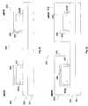
- FIG. 1Ais a perspective view of a semiconductor structure having a Silicon-On-Isolator (SOI) substrate for a non-planar strained p-MOS transistor structure fabrication according to one embodiment of the invention
- FIG. 1Bis a view similar to FIG. 1A , after a strained Si 1-x Ge x layer and an intrinsic Si layer are formed on the SOI substrate;
- FIG. 1Cis a view similar to FIG. 1B , after annealing to form a relaxed Si 1-x Ge x layer;
- FIG. 1Dis a view similar to FIG. 1C , after forming a tri-gate fin from the relaxed Si 1-x Ge x layer according to one embodiment of the invention
- FIG. 1Eis a view similar to FIG. 1D , after a strained Si 1-y Ge y layer is epitaxially formed on the relaxed Si 1-x Ge x tri-gate fin;
- FIG. 1Fis a cross-sectional view of the semiconductor structure after a high-k dielectric layer is formed on the strained Si 1-y Ge y tri-gate fin according to one embodiment of the invention
- FIG. 1Gis a cross-sectional view of the semiconductor structure after a tri-gate electrode is formed on the high-k dielectric layer according to one embodiment of the invention
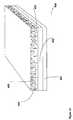
- FIG. 1His a perspective view of a tri-gate p-MOS semiconductor structure according to one embodiment of the invention.
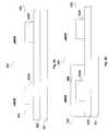
- FIG. 2Ais a cross-sectional side view of a semiconductor structure for a non-planar tri-gate CMOS fabrication with tri-gate fins according to one embodiment of the invention
- FIG. 2Bis a view similar to FIG. 2A , after covering an n-MOS portion of the semiconductor structure by a protection layer, leaving a p-MOS portion exposed;
- FIG. 2Cis a view similar to FIG. 2B , after epitaxially forming a strained Si 1-y Ge y layer on a tri-gate fin of the p-MOS portion of the semiconductor structure;
- FIG. 2Dis a view similar to FIG. 2C , after a protection oxide layer is formed on the strained Si 1-y Ge y layer covering the tri-gate fin of the p-MOS portion of the semiconductor structure;
- FIG. 2Eis a view similar to FIG. 2D , after removing the protection layer from the n-MOS portion of the semiconductor structure;
- FIG. 2Fis a view similar to FIG. 2E , after forming a strained Si layer on a tri-gate fin of the n-MOS portion of the semiconductor structure;
- FIG. 2Gis a view similar to FIG. 2F , after forming a protection pad oxide layer on the strained Si layer covering the tri-gate fin of the n-MOS portion of the semiconductor structure;
- FIG. 2His a view similar to FIG. 2G , after removing the protection oxide layers from the n-MOS and p-MOS portions of the semiconductor structure;
- FIG. 2Iis a view similar to FIG. 2H , after forming a high-k dielectric layer on the strained Si layer and Si 1-y Ge y layer;
- FIG. 2Jis a view similar to FIG. 2I , after forming a tri-gate gate electrode on the high-k dielectric layer;
- FIG. 2Kis a perspective view of the strained CMOS structure according to one embodiment of the invention.
- a non-planar strained p-MOS transistor structure and a non-planar integrated strained complementary metal-oxide-semiconductor (CMOS) structure with respective processes of their fabricationare described herein.
- a relaxed Si 1-x Ge x layeris formed on the silicon-on-isolator (SOI) substrate.
- SOIsilicon-on-isolator
- the relaxed Si 1-x Ge x layeris patterned, and subsequently, etched to form a tri-gate fin on the SOI substrate.
- a Si 1-y Ge y layerhaving a Ge content y higher than a Ge content x in the relaxed Si 1-x Ge x layer, is epitaxially formed on the tri-gate fin formed from the etched relaxed Si 1-x Ge x layer on the SOI substrate.
- the Si 1-y Ge y layercovers two opposing sidewalls and a top surface of the tri-gate fin. Due to the higher Ge content, the lattice of the Si 1-y Ge y layer has a larger spacing than the spacing of the lattice of the underlying relaxed Si 1-x Ge x layer. The larger spacing of the Si 1-y Ge y strains the Si 1-y Ge y layer, resulting in the compressive stress in the latter.
- Compressive stress in Si 1-y Ge y layersubstantially increases the hole mobility in the transistor channel of the non-planar p-MOS transistor structure improving current-voltage (I-V) characteristics.
- the I-V characteristicsare improved, for example, by increasing a saturation drain current (I DSAT ) and a linear drain current (I DLIN ) of a non-planar p-MOS transistor, as a result of increased hole mobility in the transistor channel.
- FIG. 1A of the accompanying drawingsillustrates a semiconductor structure for a non-planar strained p-MOS transistor structure fabrication according to one embodiment of the invention.
- semiconductor structure 400includes an insulating layer 402 , which is sandwiched between a silicon layer 403 and a bulk monocrystalline silicon substrate 401 forming a silicon-on-isolator (SOI) substrate.
- SOIsilicon-on-isolator
- devicesare formed in and on the layer of silicon 403 .
- the insulating layer 402may serve to reduce capacitance between the devices formed in the silicon layer 403 and the substrate 401 , resulting in less power consumption and greater circuit speed.
- the insulating layer 402is a buried oxide layer, for example, SiO 2 , and the like.
- the insulating layer 402may be any one, or a combination of, sapphire, silicon dioxide, silicon nitride, or other insulating materials.
- the thickness of the silicon layer 403may be in the approximate range of 2.5 nanometers (“nm”) to 7.5 nm.
- the thickness of the insulating layer 402may be in the approximate range of 500 angstroms (“ ⁇ ”) to 1500 ⁇ . More specifically, the thickness of the silicon layer formed on top surface of the buried oxide layer resting on the monocrystalline Si substrate, is about 5 nm and the thickness of the buried oxide layer is about 1000 ⁇ .
- the SOI substratemay be formed by any one of the techniques known in the art, for example, separation by implantation of oxygen (SIMOX), hydrogen implantation and separation approach (also called SmartCut®), and the like.
- FIG. 1Billustrates a semiconductor structure 400 after a strained Si 1-x Ge x layer and an intrinsic Si layer are formed on the SOI substrate.
- the strained Si 1-x Ge x layer 404 and an intrinsic Si layer 405are subsequently formed on the Si layer 403 .
- the Si 1-x Ge x layer 404is epitaxially grown on the Si layer 403 .
- Si 1-x Ge x materialhas a lattice structure substantially the same as a monocrystalline Si lattice structure. Because of the presence of Ge atoms, the Si 1-x Ge x lattice spacing is substantially larger than the Si lattice spacing.
- Ge atoms of the Si 1-x Ge x layer 404are diagrammed as large circles, whereas Si atoms are diagrammed as small circles in FIG. 1B .
- the lattice spacing of the Si 1-x Ge xincreases with increasing the Ge content x in the Si 1-x Ge x .
- the larger lattice spacingstrains the Si 1-x Ge x layer 404 formed on the Si layer 403 and generates the compressive stress in the Si 1-x Ge x layer 404 .
- an intrinsic Si layer 405is epitaxially grown on the strained Si 1-x Ge x layer 404 to become a capping layer for the Si 1-x Ge x layer 404 .
- the Ge content x in the Si 1-x Ge x layer 404 formed on the Si layer 403is in the approximate range of 0.05 to 0.2 (that is of 5% to 20%). In more specific embodiment, the Ge content x in the Si 1-x Ge x layer 404 on the Si layer 403 is about 0.15 that is equivalent to 15%.
- the thickness of the strained Si 1-x Ge x layer 404depends on the ultimate device geometry. In one embodiment, to form a non-planar tri-gate transistor structure, the strained Si 1-x Ge x layer 404 may have the thickness in the approximate range of 15-25 nm and the intrinsic Si layer 405 may have the thickness in the approximate range between 3 nm to 15 nm.
- the strained Si 1-x Ge x layer 404may have the thickness about 20 nm. In yet another embodiment, to form, for example, a double-gate device, the strained Si 1-x Ge x layer 404 may be about 100 nm thick.
- the heat treatment, or annealing, of the semiconductor structure 400is carried out to reduce strain of the Si 1-x Ge x layer 404 .
- Annealingresults in diffusion of the Ge atoms from Si 1-x Ge x layer 404 into the underlying Si layer 403 and upper intrinsic Si layer 405 , as illustrated in FIG. 1B .
- the diffusion of the Ge atomsrelaxes the strain in the Si 1-x Ge x layer 404 , such that the relaxed Si 1-x Ge x layer 406 is formed, as illustrated in FIG. 1C .
- the annealing temperature to relax the strained Si 1-x Ge x layer 404is in the approximate range of 1000 to 1100 C, and more specifically, about 1050 C.
- FIG. 1Cis a view of the semiconductor structure 400 after annealing.
- the semiconductor structure 400after annealing, comprises a relaxed Si 1-x Ge x layer 406 formed from the strained Si 1-x Ge x layer 404 , the Si layer 403 and the intrinsic Si layer 405 .
- the relaxed Si 1-x Ge x layer 406rests on top surface of the buried oxide layer 402 covering the silicon substrate 401 .
- the total thickness of the relaxed Si 1-x Ge x layer 406may be in the approximate range of 20 nm to 100 nm.
- the semiconductor structure 400is patterned to expose portions of the relaxed Si 1-x Ge x layer 406 .
- the exposed portions of the relaxed Si 1-x Ge x layer 406are subsequently etched and removed so that tri-gate fins in the relaxed Si 1-x Ge x layer 406 are formed.
- FIG. 1Dshows the semiconductor structure 400 with a tri-gate fin formed from relaxed Si 1-x Ge x layer on the oxide layer according to one embodiment of the invention.
- the tri-gate fin 407stands above the insulating layer 402 , the insulating layer 402 covers the Si substrate 401 .
- patterning of the relaxed Si 1-x Ge x layer 406 to form the tri-gate fin 407may be performed by using a well known in the art photolithographic technique.
- Etching the portions of the relaxed Si 1-x Ge x layer 406can be performed with an anisotropic etchant, which selectively removes the exposed portions of the relaxed Si 1-x Ge x layer 406 over the other exposed materials of the structure, generating the tri-gate fin 407 with vertical sidewalls.
- the width 421 of the tri-gate fin 407is in the approximate range of 20 nm to 120 nm.
- FIG. 1Eillustrates a strained Si 1-y Ge y 408 selectively grown on the tri-gate fin 407 .
- the strained Si 1-y Ge y layer 408covers the top surface and two opposing sidewalls of the tri-gate fin 407 , but does cover the insulating layer 402 . Because the Si 1-y Ge y layer 408 has the same lattice structure as the relaxed Si 1-x Ge x layer 406 comprising the tri-gate fin 407 , it can be epitaxially grown on the relaxed Si 1-x Ge x layer.
- the Si 1-y Ge y layerwhich is selectively grown by epitaxy on the relaxed Si 1-x Ge x tri-gate fin, has the Ge content y approximately from 0.10 to 0.50 (10% to 50%) higher than the Ge content x in the underlying relaxed Si 1-x Ge x fin.
- the Ge contenty of the Si 1-y Ge y layer epitaxially grown on the relaxed Si 1-0.15 Ge 0.15 tri-gate finis about 0.3 (30%) higher than the Ge content x in the underlying relaxed Si 1-x Ge x fin.
- the Ge content y of the Si 1-y Ge y layer epitaxially grown on the relaxed Si 1-0.15 Ge 0.15 tri-gate finis about 0.3 (30%).
- the higher Ge contentmeans larger lattice spacing of the Si 1-y Ge y layer relative to the relaxed Si 1-x Ge x layer. Larger lattice spacing creates compressive stress in the Si 1-y Ge y layer covering the top surface and two opposing sidewalls of the relaxed Si 1-x Ge x tri-gate fin.
- the compressive stress in the Si 1-y Ge y layerreduces the effective mass of the p-type carriers (holes) that substantially increases the hole mobility in a channel of the non-planar PMOS transistor, wherein the channel is formed in the strained Si 1-y Ge y layer 408 .
- the hole mobility enhancement factor in the channel formed in the strained Si 1-y Ge y layer 408is in the approximate range of 1.2 to 5.
- the strained Si 1-y Ge y layer 408may be epitaxially grown on the tri-gate fin 407 by a low pressure chemical vapour deposition (CVD) technique including Silane (SiH4) and Germane (GeH 4 ) gases.
- the strained Si 1-y Ge y layer 408may be epitaxially grown on the relaxed Si 1-x Ge x tri-gate fin 407 by a low pressure chemical vapour deposition (CVD) technique including DichloroSilane (SiCl 2 H 2 ) and Germane (GeH 4 ) gases.
- the pressure in the reactormay be in the approximate range of 1 torr to 400 torr and the temperature may be in the approximate range of 300 C to 900 C.
- the thickness of the strained Si 1-y Ge y layer selectively grown by epitaxy on the relaxed Si 1-x Ge x tri-gate finis in the approximate range of 50 ⁇ to 200 ⁇ . More specifically, the thickness of the strained Si 1-y Ge y layer is about 100 ⁇ .
- a n-type dopantfor example, arsenic (“As”), phosphorus (“P”), and the like, is added to the relaxed Si 1-x Ge x tri-gate fin 407 covered by the strained Si 1-y Ge y layer 408 to form a n-well.
- the n-type dopantmay be added by using, for example, the ion implantation technique.
- the concentration of the n-type dopantsis in the approximate range of 2 ⁇ 10 16 cm ⁇ 3 to 2 ⁇ 10 19 cm ⁇ 3 .
- a dielectric layeris formed on the strained Si 1-y Ge y layer.
- the dielectric layer 409covers the top surface and two opposing sidewalls of the tri-gate fin 407 with the strained Si 1-y Ge y layer 408 .
- the dielectric layer 409forms a gate dielectric of the tri-gate transistor structure.
- the dielectric layer 409may be blanket deposited, patterned, and etched into the gate dielectric utilizing known photolithographic and etching techniques.
- the dielectric layermay include oxide of a transition metal.
- the dielectric layer 409may include a high-k dielectric, for example, zirconium oxide(“ZrO 2 ”).
- the dielectric layer 409may include of any one of a hafnium oxide(“HFO 2 ”) and lanthanum oxide (“La 2 O 4 ”).
- the thickness of the dielectric layer 409may be between 10 ⁇ and 40 ⁇ .
- FIG. 1Gis a cross-sectional view of the semiconductor structure 400 after a tri-gate electrode layer is formed on the high-k dielectric layer according to one embodiment of the invention.
- the tri-gate electrode layer 411is formed on the dielectric layer 409 covering the top surface and the sidewalls of the tri-gate fin 407 , as illustrated in FIG. 1G .
- the thickness of the tri-gate electrode layer 411is in the approximate range of 500 ⁇ to 1500 ⁇ .
- the tri-gate electrode layer 411may be formed by blanket deposition of polysilicon and patterning the polysilicon into the tri-gate electrode utilizing known photolithographic techniques.
- the tri-gate electrode layer 411 and the underlying dielectric layer 409may be subsequently patterned and etched to a predetermined width.
- the tri-gate electrode layer 411includes a metal underlayer under the polysilicon.
- the tri-gate electrode layer 411is a metal.
- FIG. 1His a perspective view of a tri-gate p-MOS semiconductor structure 400 according to one embodiment of the invention.
- the structure 400has a source region 413 and a drain region 414 formed in the fin structure (“fin body”) 418 at opposite sides of the gate electrode 421 .
- the gate electrode 421 with underlying dielectric 429has a predetermined width 415 and covers a portion of the fin body 418 .
- the fin body 418includes a tri-gate fin 407 formed from relaxed Si 1-x Ge x layer covered by the strained Si 1-y Ge y layer 408 .
- the fin body 418is formed on top surface of the insulating layer 402 .
- the insulating layer 402rests on the silicon substrate 401 .
- the width 415 of the gate electrode 421is in the approximate range of 80 nm to 120 nm
- the thickness 416 of the fin body 418is in the approximate range of 20 nm to 120 nm
- the width 417 of the fin body 418is in the approximate range of 20 nm to 120 nm.
- a p-type dopantfor example, boron (“B”) is added to the fin body 418 at the opposite sides of the gate electrode 421 , for example, by ion implantation.
- the concentration of the p-type dopantsis in the approximate range of 10 18 cm ⁇ 3 to 10 21 cm ⁇ 3 .
- FIGS. 2A-2Killustrate an exemplary process to fabricate a strained non-planar tri-gate CMOS structure, according to one embodiment of the invention.
- FIG. 2Aillustrates a cross-sectional view of the semiconductor structure 500 for tri-gate CMOS fabrication with two tri-gate fins 503 N and 503 P formed from a relaxed Si 1-x Ge x layer. As shown in FIG. 2A , the tri-gate fins 503 N and 503 P formed from a relaxed Si 1-x Ge x layer are located on an oxide layer 502 , which covers a Si substrate 501 .
- One of the tri-gate fins 503 Nbelongs to an n-MOS portion 520 of the semiconductor structure, whereas the other tri-gate fin 503 P belongs to a p-MOS portion 530 of the CMOS structure.
- Semiconductor structure 500 having tri-gate fins 503 N and 503 P formed from the relaxed Si 1-x Ge x layermay be fabricated using the process described presently.
- the n-MOS portion 520is covered by a first protection layer to protect the n-MOS portion during p-MOS portion formation.
- FIG. 2Bis a cross-sectional view of the semiconductor structure 500 after covering the n-MOS portion by a first protection layer.
- the p-MOS portion 530 of the structure 500is uncovered, while the first protection layer 505 covers the top surface and sidewalls of the tri-gate fin 503 N that belongs to the n-MOS portion 520 .
- the first protection layer 505may be formed, for example, by depositing a silicon nitride (“Si 3 N 4 ”) layer on the wafer, forming a resist on the Si 3 N 4 layer, patterning the resist to expose portions of the Si 3 N 4 layer covering the p-MOS portion 530 , etching the silicon nitride layer on the p-MOS portion 530 to expose p-MOS portion 530 , and then ashing the resist producing the structure in FIG. 2B .
- other implant mask materialsmay be used as a first protection layer 505 .
- a strained Si 1-y Ge y layeris selectively formed on the tri-gate fin 503 P of the p-MOS portion 530 .
- FIG. 2Cshows a cross-sectional view of the semiconductor structure 500 after epitaxially forming a strained Si 1-y Ge y layer on the tri-gate fin of the p-MOS portion.
- the n-MOS portion 520is covered by the first protection layer 505 .
- the strained Si 1-y Ge y layer 504covers the top surface and two opposing sidewalls of the tri-gate fin 503 P of the p-MOS portion 530 of the structure 500 leaving the oxide layer 502 uncovered.
- the strained Si 1-y Ge y layer 504is selectively epitaxially grown on the top surface and two opposing sidewalls of the tri-gate fin 503 P of the p-MOS portion 530 .
- the strained Si 1-y Ge y layer 504is grown by low pressure CVD technique with a flow including SiH 4 and GeH 4 gases.
- the strained Si 1-y Ge y layer 504may be epitaxially grown by a low-pressure chemical vapour CVD with a flow including of SiCl 2 H 2 and GeH 4 gases.
- the pressure in the reactormay be in the approximate range of 1 torr to 400 torr and the temperature may be in the approximate range of 300 C to 900 C.
- the strained Si 1-y Ge y layer 504has a Ge content y approximately 15% higher than the Ge content x of the relaxed Si 1-x Ge x layer of the tri-gate fin 503 P and a lattice spacing substantially larger than the lattice spacing of the Si 1-x Ge x layer of the tri-gate fin 503 P that results in a compressive stress in the strained Si 1-y Ge y layer 504 along the top surface and two opposing sidewalls of the tri-gate fin 503 P of the p-MOS portion 530 .
- the strained Si 1-y Ge y layer 504has the Ge content y about 10% to 50% higher than the relaxed Si 1-x Ge x layer of the tri-gate fin 503 P.
- the strained Si 1-y Ge y layer 504has the Ge content y about 0.3 (30%) and the relaxed Si 1-x Ge x layer of the tri-gate fin 503 P has the Ge content x of about 0.15 (15%).
- the compressive stressincreases the hole mobility in the strained Si 1-y Ge y layer 504 .
- the hole mobility enhancement factor in the channel formed in the strained Si 1-y Ge y layer 408is in the approximate range of 1.2 to 5.
- the thickness of the strained Si 1-y Ge y layer 504is in the approximate range of 50 ⁇ to 200 ⁇ , and more specifically, about 100 ⁇ .
- a n-type dopantis added to the tri-gate fin 503 N covered by the strained Si 1-y Ge y layer 504 .
- the n-type dopantmay be any one of As, P, and the like.
- the n-type dopantmay be added, for example, by the ion implantation technique.
- the concentration of the dopantsis in the approximate range of 2 ⁇ 10 17 cm ⁇ 3 to 2 ⁇ 10 19 cm ⁇ 3 .
- the strained Si 1-y Ge y layer 504may be covered by a second protection layer to protect the surface of the strained Si 1-y Ge y layer 504 from unnecessary damage.
- FIG. 2Dis a cross-sectional view of the semiconductor structure 500 having a second protection layer 506 formed on the strained Si 1-y Ge y layer.
- the second protection layer 506is deposited on the strained Si 1-y Ge y layer 504 along the top surface and two opposing sidewalls of the tri-gate fin 503 P of the p-MOS portion 530 .
- the second protection layer 506may be a silicon oxide layer formed by the epitaxial growth and the subsequent oxidation of silicon.
- the second protection layer 506may be a second silicon nitride layer formed by patterning and etching technique, which is known to one of ordinary skill in the art of semiconductor fabrication.
- the protection layer 506may be formed by repeating the deposition of silicon nitride layer on the wafer, lithographically patterning the silicon nitride layer to leave a resist on the p-MOS portion 530 , etching the silicon nitride layer off the n-MOS portion 520 , and then stripping off the resist.
- the second protection layer 506also protects the p-MOS portion 530 from, for example, unnecessary deposition of Si during the strained channel formation at the n-MOS portion 520 of the semiconductor structure 500 .
- the thickness of the second protection layer 506may be in the approximate range of 30 ⁇ to 100 ⁇ .
- the first protection layer 505is removed from the n-MOS portion 520 of the semiconductor structure 500 .
- FIG. 2Eis a cross-sectional view of the semiconductor structure 500 , after removing the first protection layer 505 from the n-MOS portion of the semiconductor structure 500 .
- the first protection layer 505may be removed by, for example, wet etching using a hot phosphoric acid.
- the strained Si layeris epitaxially grown on the tri-gate fin 503 N of the n-MOS portion 520 .
- FIG. 2Fis a cross-sectional view of the semiconductor structure after forming a strained Si layer on the tri-gate fin of the n-MOS portion.
- the strained Si layer 507covers the top surface and two opposing sidewalls of the fin tri-gate 503 N of the n-MOS portion 520 of the semiconductor structure 500 and does not cover the oxide layer 502 .
- the strained Si layer 507may be formed by the epitaxy.
- the Si 1-x Ge x layer of the tri-gate fin 503 Nhas substantially larger lattice spacing, than the lattice spacing of the Si layer, resulting in a tensile strain in the Si layer along the top surface and two opposing sidewalls of the tri-gate fin 503 N of the n-MOS portion 520 .
- the tensile strainincreases the electron mobility in the strained Si layer 507 of the n-MOS portion 520 of the semiconductor structure 500 .
- the electron mobility enhancement factor in the channel formed in the strained Si layer 507is in the approximate range of 1.2 to 5.
- the thickness of the strained Si layer 507is in the approximate range of 50 ⁇ to 200 ⁇ , and more specifically, about 100 ⁇ .
- a p-wellis formed in the n-MOS portion 520 .
- a p-type dopantfor example, B, and the like, is added to the tri-gate fin 503 N covered by the strained Si layer 507 by the ion implantation technique.
- the pad oxide layeris formed on the strained Si layer, covering the top surface and two opposing sidewalls of the tri-gate fin 503 N.
- concentration of p-dopantsis in the approximate range of 2 ⁇ 10 17 cm ⁇ 3 to 2 ⁇ 10 19 cm ⁇ 3 .
- FIG. 2Gis a cross-sectional view of the semiconductor structure 500 after forming a pad oxide layer.
- the pad oxide layer 508is formed on the strained Si layer 507 covering the tri-gate fin 503 N of the n-MOS portion 530 .
- the pad oxide layer 508covers the strained Si layer 507 along the top surface and two opposing sidewalls of the tri-gate fin 503 N.
- the pad oxide layer 508is a silicon oxide.
- the second protection layer 506 and the pad oxide layer 508are removed from the n-MOS portion 520 and the p-MOS 530 portion, respectively.
- FIG. 2His a cross-sectional view of the semiconductor structure 500 after removing the oxide layers from the n-MOS and p-MOS portions.
- the second protection layer 506 and the pad oxide layer 508may be removed by, for example, wet etching.
- a dielectric layeris formed on the strained Si and Si 1-y Ge y layers.
- FIG. 2Iis a cross-sectional view of semiconductor structure 500 after forming a dielectric layer on the strained Si layer and Si 1-y Ge y layer, which respectively covers the tri-gate fins of each of the n-MOS and p-MOS portions.
- the dielectric layer 509is deposited on the strained Si layer 507 and the strained Si 1-y Ge y layer 504 , covering the top surface and two opposing sidewalls of the tri-gate fins 503 N and 503 P of the n-MOS portion 520 and the p-MOS 530 portion respectively, as illustrated in FIG. 21 .
- the dielectric layer 509may be blanket deposited, patterned, and etched into the gate dielectric using known photolithographic and etching techniques.
- the dielectric layer 509is a high-k dielectric.
- the dielectric layer 509may include an oxide
- the dielectric layer 509may include an oxide of transition metal.
- the dielectric layer 509may be made of ZrO 2 , HFO 2 , or La 2 O 5 or any combination thereof.
- the dielectric layer 509may be formed to the thickness in the approximate range of 10 ⁇ to 40 ⁇ .
- the tri-gate electrode layeris formed on the dielectric layer 509 .
- FIG. 2Jis a cross-sectional view of the semiconductor structure 500 , after forming a tri-gate electrode layer.
- the tri-gate electrode layer 510is formed on the gate dielectric layer 509 covering the top surface and two opposing sidewalls of each of the tri-gate fins 503 N and 503 P of the n-MOS 520 portion and the p-MOS portion 530 .
- the thickness of the tri-gate electrode layer 510is in the approximate range of 500 ⁇ to 1500 ⁇ .
- the tri-gate electrode layer 510may be formed by blanket deposition of polysilicon. Then, the tri-gate electrode layer 510 may be patterned and etched into the tri-gate electrode using known in the art photolithographic and etching techniques.
- the tri-gate electrode layer 510 with the underlying dielectric layer 509are patterned and etched to a predetermined width.
- FIG. 2Kis a perspective view of the non-planar tri-gate CMOS structure 600 according to one embodiment of the invention.
- the CMOS structure 600has the n-MOS portion 520 and the p-MOS portion 530 .
- the n-MOS portion 520has a source region 523 and a drain region 524 formed in the portions of n-MOS fin structure (“n-MOS fin body”) 525 at opposite sides of the gate electrode 521 .
- the n-MOS gate electrode 521 with the underlying dielectric layer 509has the width 542 and covers the top surface and two opposing sidewalls of the n-MOS fin body 525 .
- the n-MOS fin body 525is formed on top surface of the oxide layer 502 .
- the oxide layer 502covers the silicon substrate 501 .
- the n-MOS fin body 525includes a relaxed Si 1-x Ge x layer covered by the tensile strained Si layer.
- a strained channel of the n-MOS portion 527is formed in the tensile strained Si layer under the dielectric layer 509 along the top surface and the two opposing sidewalls of the fin body 525 .
- a n-type dopantfor example, arsenic (“As”) is added into the fin body 525 on the opposite sides of the gate electrode 521 on the n-MOS portion 520 of the CMOS structure 600 .
- the n-type dopantmay be added by, for example, the ion implantation.
- the concentration of n-dopantsmaybe in the approximate range of 10 18 cm ⁇ 3 to 10 21 cm ⁇ 3 .
- the p-MOS portion 530has a source region 533 and a drain region 534 formed in the p-MOS fin body 535 on opposite sides of the gate electrode 531 .
- the p-MOS gate electrode 531 with underlying dielectric layer 509has the predetermined width 542 and covers the top surface and the two opposing sidewalls of the p-MOS fin body 535 .
- the p-MOS fin body 535is formed on top surface of the oxide layer 502 .
- the oxide layer 502covers the silicon substrate 501 .
- the p-MOS fin body 535 of the p-MOS portionincludes the relaxed Si 1-x Ge x layer, wherein the top surface and two opposing sidewalls of the relaxed Si 1-x Ge x layer are covered by the compressively strained Si 1-y Ge y layer.
- a strained channel 537 of the p-MOS portion 530is formed in the compressively strained Si 1-y Ge y layer under the gate dielectric layer 509 along the top surface and the two opposing sidewalls of the p-MOS fin body 535 .
- a p-type dopantfor example, boron (“B”) is added into the p-MOS fin body 535 at the opposite sides of the gate electrode 531 on the p-MOS portion 530 of the CMOS structure 600 .
- the p-type dopantmay be added by, for example, the ion implantation.
- the concentration of p-dopantsmay be in the approximate range of 10 18 cm ⁇ 3 to 10 21 cm ⁇ 3 .
- the width 542 of the n-MOS tri-gate electrode 521 and the p-MOS tri-gate electrode 531 with the underlying dielectric 509may be in the approximate range of 30 nm to 120 nm each.
- the width 541 of the n-MOS fin body 525 and the p-MOS fin body 535may be in the approximate range of 30 nm to 120 nm each.
- the thickness 543 of the n-MOS fin body 525 and the p-MOS fin body 535may be in the approximate range of 20 nm to 120 nm each.
Landscapes
- Insulated Gate Type Field-Effect Transistor (AREA)
- Thin Film Transistor (AREA)
- Metal-Oxide And Bipolar Metal-Oxide Semiconductor Integrated Circuits (AREA)
Abstract
Description
- 1. Field of the Invention
- This invention relates to the field of semiconductor manufacturing, and more specifically, to a semiconductor transistor and its manufacture.
- 2. Discussion of Related Art
- Various techniques are used to improve performance of a metal-oxide-semiconductor (MOS) transistor. Transistors have continuously been scaled down, thus increasing their density, and accordingly, their switching speeds.
- Another way to increase the speed of the transistor, is to create a transistor channel with a high mobility of the carriers by, for example, growing a strained silicon (Si) layer on a relaxed silicon germanium (“Si1-xGex”) layer thereby increasing mobility of electrons. The tensile strain in the Si layer, however, does not increase the hole mobility. Therefore, for a p-MOS transistor structure, the channel formed from the Si layer under tensile stress cannot provide increased hole mobility. In addition, the tensile strained Si layer is grown on a planar substrate, which limits the density of the transistors and increases intrinsic capacitance.
- The invention is described by way of example with reference to the accompanying drawings, wherein:
FIG. 1A is a perspective view of a semiconductor structure having a Silicon-On-Isolator (SOI) substrate for a non-planar strained p-MOS transistor structure fabrication according to one embodiment of the invention;FIG. 1B is a view similar toFIG. 1A , after a strained Si1-xGexlayer and an intrinsic Si layer are formed on the SOI substrate;FIG. 1C is a view similar toFIG. 1B , after annealing to form a relaxed Si1-x Gexlayer;FIG. 1D is a view similar toFIG. 1C , after forming a tri-gate fin from the relaxed Si1-xGexlayer according to one embodiment of the invention;FIG. 1E is a view similar toFIG. 1D , after a strained Si1-yGeylayer is epitaxially formed on the relaxed Si1-xGextri-gate fin;FIG. 1F is a cross-sectional view of the semiconductor structure after a high-k dielectric layer is formed on the strained Si1-yGeytri-gate fin according to one embodiment of the invention;FIG. 1G is a cross-sectional view of the semiconductor structure after a tri-gate electrode is formed on the high-k dielectric layer according to one embodiment of the invention;FIG. 1H is a perspective view of a tri-gate p-MOS semiconductor structure according to one embodiment of the invention;FIG. 2A is a cross-sectional side view of a semiconductor structure for a non-planar tri-gate CMOS fabrication with tri-gate fins according to one embodiment of the invention;FIG. 2B is a view similar toFIG. 2A , after covering an n-MOS portion of the semiconductor structure by a protection layer, leaving a p-MOS portion exposed;FIG. 2C is a view similar toFIG. 2B , after epitaxially forming a strained Si1-yGeylayer on a tri-gate fin of the p-MOS portion of the semiconductor structure;FIG. 2D is a view similar toFIG. 2C , after a protection oxide layer is formed on the strained Si1-yGeylayer covering the tri-gate fin of the p-MOS portion of the semiconductor structure;FIG. 2E is a view similar toFIG. 2D , after removing the protection layer from the n-MOS portion of the semiconductor structure;FIG. 2F is a view similar toFIG. 2E , after forming a strained Si layer on a tri-gate fin of the n-MOS portion of the semiconductor structure;FIG. 2G is a view similar toFIG. 2F , after forming a protection pad oxide layer on the strained Si layer covering the tri-gate fin of the n-MOS portion of the semiconductor structure;FIG. 2H is a view similar toFIG. 2G , after removing the protection oxide layers from the n-MOS and p-MOS portions of the semiconductor structure;FIG. 2I is a view similar toFIG. 2H , after forming a high-k dielectric layer on the strained Si layer and Si1-yGeylayer;FIG. 2J is a view similar toFIG. 2I , after forming a tri-gate gate electrode on the high-k dielectric layer; andFIG. 2K is a perspective view of the strained CMOS structure according to one embodiment of the invention.- A non-planar strained p-MOS transistor structure and a non-planar integrated strained complementary metal-oxide-semiconductor (CMOS) structure with respective processes of their fabrication are described herein. A relaxed Si1-xGexlayer is formed on the silicon-on-isolator (SOI) substrate. The relaxed Si1-xGexlayer is patterned, and subsequently, etched to form a tri-gate fin on the SOI substrate. Further, a Si1-yGeylayer, having a Ge content y higher than a Ge content x in the relaxed Si1-xGexlayer, is epitaxially formed on the tri-gate fin formed from the etched relaxed Si1-xGexlayer on the SOI substrate. The Si1-yGeylayer covers two opposing sidewalls and a top surface of the tri-gate fin. Due to the higher Ge content, the lattice of the Si1-yGeylayer has a larger spacing than the spacing of the lattice of the underlying relaxed Si1-xGexlayer. The larger spacing of the Si1-yGeystrains the Si1-yGeylayer, resulting in the compressive stress in the latter. A compressively stressed Si1-yGeylayer epitaxially grown on the top surface and the two opposing sidewalls of the tri-gate fin formed from the relaxed Si1-xGexlayer, which rests on the SOI substrate, is used to form a strained channel between a source and drain region of the non-planar p-MOS transistor structure. Compressive stress in Si1-yGeylayer substantially increases the hole mobility in the transistor channel of the non-planar p-MOS transistor structure improving current-voltage (I-V) characteristics. The I-V characteristics are improved, for example, by increasing a saturation drain current (IDSAT) and a linear drain current (IDLIN) of a non-planar p-MOS transistor, as a result of increased hole mobility in the transistor channel.
FIG. 1A of the accompanying drawings illustrates a semiconductor structure for a non-planar strained p-MOS transistor structure fabrication according to one embodiment of the invention. As shown inFIG. 1A ,semiconductor structure 400 includes an insulatinglayer 402, which is sandwiched between asilicon layer 403 and a bulkmonocrystalline silicon substrate 401 forming a silicon-on-isolator (SOI) substrate. Generally, devices are formed in and on the layer ofsilicon 403. The insulatinglayer 402 may serve to reduce capacitance between the devices formed in thesilicon layer 403 and thesubstrate 401, resulting in less power consumption and greater circuit speed. In one embodiment, the insulatinglayer 402 is a buried oxide layer, for example, SiO2, and the like. In alternative embodiments, the insulatinglayer 402 may be any one, or a combination of, sapphire, silicon dioxide, silicon nitride, or other insulating materials. The thickness of thesilicon layer 403 may be in the approximate range of 2.5 nanometers (“nm”) to 7.5 nm. The thickness of the insulatinglayer 402 may be in the approximate range of 500 angstroms (“Å”) to 1500 Å. More specifically, the thickness of the silicon layer formed on top surface of the buried oxide layer resting on the monocrystalline Si substrate, is about 5 nm and the thickness of the buried oxide layer is about 1000 Å. The SOI substrate may be formed by any one of the techniques known in the art, for example, separation by implantation of oxygen (SIMOX), hydrogen implantation and separation approach (also called SmartCut®), and the like.FIG. 1B illustrates asemiconductor structure 400 after a strained Si1-xGexlayer and an intrinsic Si layer are formed on the SOI substrate. The strained Si1-xGexlayer404 and anintrinsic Si layer 405 are subsequently formed on theSi layer 403. The Si1-xGexlayer404 is epitaxially grown on theSi layer 403. Generally, Si1-xGexmaterial has a lattice structure substantially the same as a monocrystalline Si lattice structure. Because of the presence of Ge atoms, the Si1-xGexlattice spacing is substantially larger than the Si lattice spacing. Ge atoms of the Si1-xGexlayer404 are diagrammed as large circles, whereas Si atoms are diagrammed as small circles inFIG. 1B . The lattice spacing of the Si1-xGexincreases with increasing the Ge content x in the Si1-xGex. The larger lattice spacing strains the Si1-xGexlayer404 formed on theSi layer 403 and generates the compressive stress in the Si1-xGexlayer404. In one embodiment, anintrinsic Si layer 405 is epitaxially grown on the strained Si1-xGexlayer404 to become a capping layer for the Si1-xGexlayer404. In one embodiment, the Ge content x in the Si1-xGexlayer404 formed on theSi layer 403 is in the approximate range of 0.05 to 0.2 (that is of 5% to 20%). In more specific embodiment, the Ge content x in the Si1-xGexlayer404 on theSi layer 403 is about 0.15 that is equivalent to 15%. Generally, the thickness of the strained Si1-xGexlayer404 depends on the ultimate device geometry. In one embodiment, to form a non-planar tri-gate transistor structure, the strained Si1-xGexlayer404 may have the thickness in the approximate range of 15-25 nm and theintrinsic Si layer 405 may have the thickness in the approximate range between 3 nm to 15 nm. In another embodiment, the strained Si1-xGexlayer404 may have the thickness about 20 nm. In yet another embodiment, to form, for example, a double-gate device, the strained Si1-xGexlayer404 may be about 100 nm thick.- The heat treatment, or annealing, of the
semiconductor structure 400 is carried out to reduce strain of the Si1-xGexlayer404. Annealing results in diffusion of the Ge atoms from Si1-xGexlayer404 into theunderlying Si layer 403 and upperintrinsic Si layer 405, as illustrated inFIG. 1B . The diffusion of the Ge atoms relaxes the strain in the Si1-xGexlayer404, such that the relaxed Si1-xGexlayer406 is formed, as illustrated inFIG. 1C . In one embodiment, the annealing temperature to relax the strained Si1-xGexlayer404 is in the approximate range of 1000 to 1100 C, and more specifically, about 1050 C. FIG. 1C is a view of thesemiconductor structure 400 after annealing. As shown inFIG. 1C , thesemiconductor structure 400, after annealing, comprises a relaxed Si1-xGexlayer406 formed from the strained Si1-xGexlayer404, theSi layer 403 and theintrinsic Si layer 405. The relaxed Si1-xGexlayer406 rests on top surface of the buriedoxide layer 402 covering thesilicon substrate 401. In one embodiment, the total thickness of the relaxed Si1-xGexlayer406 may be in the approximate range of 20 nm to 100 nm.- The
semiconductor structure 400 is patterned to expose portions of the relaxed Si1-xGexlayer406. The exposed portions of the relaxed Si1-xGexlayer406 are subsequently etched and removed so that tri-gate fins in the relaxed Si1-xGexlayer406 are formed.FIG. 1D shows thesemiconductor structure 400 with a tri-gate fin formed from relaxed Si1-xGexlayer on the oxide layer according to one embodiment of the invention. Thetri-gate fin 407 stands above the insulatinglayer 402, the insulatinglayer 402 covers theSi substrate 401. In one embodiment, patterning of the relaxed Si1-xGexlayer406 to form thetri-gate fin 407 may be performed by using a well known in the art photolithographic technique. Etching the portions of the relaxed Si1-xGexlayer406 can be performed with an anisotropic etchant, which selectively removes the exposed portions of the relaxed Si1-xGexlayer406 over the other exposed materials of the structure, generating thetri-gate fin 407 with vertical sidewalls. In one embodiment, thewidth 421 of thetri-gate fin 407 is in the approximate range of 20 nm to 120 nm. FIG. 1E illustrates a strained Si1-yGey408 selectively grown on thetri-gate fin 407. The strained Si1-yGeylayer408 covers the top surface and two opposing sidewalls of thetri-gate fin 407, but does cover the insulatinglayer 402. Because the Si1-yGeylayer408 has the same lattice structure as the relaxed Si1-xGexlayer406 comprising thetri-gate fin 407, it can be epitaxially grown on the relaxed Si1-xGexlayer. In one embodiment, the Si1-yGeylayer, which is selectively grown by epitaxy on the relaxed Si1-xGextri-gate fin, has the Ge content y approximately from 0.10 to 0.50 (10% to 50%) higher than the Ge content x in the underlying relaxed Si1-xGexfin. In another embodiment, the Ge contenty of the Si1-yGeylayer epitaxially grown on the relaxed Si1-0.15Ge0.15tri-gate fin is about 0.3 (30%) higher than the Ge content x in the underlying relaxed Si1-xGexfin. In yet another embodiment, the Ge content y of the Si1-yGeylayer epitaxially grown on the relaxed Si1-0.15Ge0.15tri-gate fin is about 0.3 (30%). Generally, the higher Ge content means larger lattice spacing of the Si1-yGeylayer relative to the relaxed Si1-xGexlayer. Larger lattice spacing creates compressive stress in the Si1-yGeylayer covering the top surface and two opposing sidewalls of the relaxed Si1-xGextri-gate fin. The compressive stress in the Si1-yGeylayer reduces the effective mass of the p-type carriers (holes) that substantially increases the hole mobility in a channel of the non-planar PMOS transistor, wherein the channel is formed in the strained Si1-yGeylayer408. In one embodiment, the hole mobility enhancement factor in the channel formed in the strained Si1-yGeylayer408 is in the approximate range of 1.2 to 5.- In one embodiment, the strained Si1-yGeylayer408 may be epitaxially grown on the
tri-gate fin 407 by a low pressure chemical vapour deposition (CVD) technique including Silane (SiH4) and Germane (GeH4) gases. For another embodiment, the strained Si1-yGeylayer408 may be epitaxially grown on the relaxed Si1-xGextri-gate fin 407 by a low pressure chemical vapour deposition (CVD) technique including DichloroSilane (SiCl2H2) and Germane (GeH4) gases. In one embodiment, the pressure in the reactor may be in the approximate range of 1 torr to 400 torr and the temperature may be in the approximate range of 300 C to 900 C. In one embodiment, the thickness of the strained Si1-yGeylayer selectively grown by epitaxy on the relaxed Si1-xGextri-gate fin is in the approximate range of 50 Å to 200 Å. More specifically, the thickness of the strained Si1-yGeylayer is about 100 Å. Further, a n-type dopant, for example, arsenic (“As”), phosphorus (“P”), and the like, is added to the relaxed Si1-xGextri-gate fin 407 covered by the strained Si1-yGeylayer408 to form a n-well. The n-type dopant may be added by using, for example, the ion implantation technique. The concentration of the n-type dopants is in the approximate range of 2×1016cm−3to 2×1019cm−3. - As illustrated in
FIG. 1F , a dielectric layer is formed on the strained Si1-yGeylayer. Thedielectric layer 409 covers the top surface and two opposing sidewalls of thetri-gate fin 407 with the strained Si1-yGeylayer408. Thedielectric layer 409 forms a gate dielectric of the tri-gate transistor structure. In one embodiment, thedielectric layer 409 may be blanket deposited, patterned, and etched into the gate dielectric utilizing known photolithographic and etching techniques. In one embodiment, the dielectric layer may include oxide of a transition metal. In one embodiment, thedielectric layer 409 may include a high-k dielectric, for example, zirconium oxide(“ZrO2”). For alternative embodiments, thedielectric layer 409 may include of any one of a hafnium oxide(“HFO2”) and lanthanum oxide (“La2O4”). The thickness of thedielectric layer 409 may be between 10 Å and 40Å. FIG. 1G is a cross-sectional view of thesemiconductor structure 400 after a tri-gate electrode layer is formed on the high-k dielectric layer according to one embodiment of the invention. Thetri-gate electrode layer 411 is formed on thedielectric layer 409 covering the top surface and the sidewalls of thetri-gate fin 407, as illustrated inFIG. 1G . In one embodiment, the thickness of thetri-gate electrode layer 411 is in the approximate range of 500 Å to 1500 Å. In one embodiment, thetri-gate electrode layer 411 may be formed by blanket deposition of polysilicon and patterning the polysilicon into the tri-gate electrode utilizing known photolithographic techniques. For an embodiment, thetri-gate electrode layer 411 and theunderlying dielectric layer 409 may be subsequently patterned and etched to a predetermined width. In another embodiment, thetri-gate electrode layer 411 includes a metal underlayer under the polysilicon. In yet another embodiment, thetri-gate electrode layer 411 is a metal.FIG. 1H is a perspective view of a tri-gate p-MOS semiconductor structure 400 according to one embodiment of the invention. Thestructure 400 has asource region 413 and a drain region414 formed in the fin structure (“fin body”)418 at opposite sides of thegate electrode 421. Thegate electrode 421 withunderlying dielectric 429 has apredetermined width 415 and covers a portion of the fin body418. For an embodiment, the fin body418 includes atri-gate fin 407 formed from relaxed Si1-xGexlayer covered by the strained Si1-yGeylayer408. The fin body418 is formed on top surface of the insulatinglayer 402. The insulatinglayer 402 rests on thesilicon substrate 401. In one embodiment, thewidth 415 of thegate electrode 421 is in the approximate range of 80 nm to 120 nm, the thickness416 of the fin body418 is in the approximate range of 20 nm to 120 nm, and the width417 of the fin body418 is in the approximate range of 20 nm to 120 nm. For an embodiment, to form thesource region 413 and the drain region414 of the p-MOS transistor structure 400, a p-type dopant, for example, boron (“B”) is added to the fin body418 at the opposite sides of thegate electrode 421, for example, by ion implantation. For an embodiment, the concentration of the p-type dopants is in the approximate range of 1018cm−3to 1021cm−3.FIGS. 2A-2K illustrate an exemplary process to fabricate a strained non-planar tri-gate CMOS structure, according to one embodiment of the invention.FIG. 2A illustrates a cross-sectional view of thesemiconductor structure 500 for tri-gate CMOS fabrication with twotri-gate fins FIG. 2A , thetri-gate fins oxide layer 502, which covers aSi substrate 501. One of thetri-gate fins 503N belongs to an n-MOS portion 520 of the semiconductor structure, whereas the othertri-gate fin 503P belongs to a p-MOS portion 530 of the CMOS structure.Semiconductor structure 500 havingtri-gate fins MOS portion 530, the n-MOS portion 520 is covered by a first protection layer to protect the n-MOS portion during p-MOS portion formation.FIG. 2B is a cross-sectional view of thesemiconductor structure 500 after covering the n-MOS portion by a first protection layer. The p-MOS portion 530 of thestructure 500 is uncovered, while thefirst protection layer 505 covers the top surface and sidewalls of thetri-gate fin 503N that belongs to the n-MOS portion 520. For an embodiment, thefirst protection layer 505 may be formed, for example, by depositing a silicon nitride (“Si3N4”) layer on the wafer, forming a resist on the Si3N4layer, patterning the resist to expose portions of the Si3N4layer covering the p-MOS portion 530, etching the silicon nitride layer on the p-MOS portion 530 to expose p-MOS portion 530, and then ashing the resist producing the structure inFIG. 2B . In alternative embodiments, other implant mask materials may be used as afirst protection layer 505. Next, to form a strained channel in the p-MOS portion 530 of thesemiconductor structure 500, a strained Si1-yGeylayer is selectively formed on thetri-gate fin 503P of the p-MOS portion 530.FIG. 2C shows a cross-sectional view of thesemiconductor structure 500 after epitaxially forming a strained Si1-yGeylayer on the tri-gate fin of the p-MOS portion. The n-MOS portion 520 is covered by thefirst protection layer 505. The strained Si1-yGeylayer504 covers the top surface and two opposing sidewalls of thetri-gate fin 503P of the p-MOS portion 530 of thestructure 500 leaving theoxide layer 502 uncovered. In one embodiment, the strained Si1-yGeylayer504 is selectively epitaxially grown on the top surface and two opposing sidewalls of thetri-gate fin 503P of the p-MOS portion 530. More specifically, the strained Si1-yGeylayer504 is grown by low pressure CVD technique with a flow including SiH4and GeH4gases. For another embodiment, the strained Si1-yGeylayer504 may be epitaxially grown by a low-pressure chemical vapour CVD with a flow including of SiCl2H2and GeH4gases. The pressure in the reactor may be in the approximate range of 1 torr to 400 torr and the temperature may be in the approximate range of 300 C to 900 C.- The strained Si1-yGeylayer504 has a Ge content y approximately 15% higher than the Ge content x of the relaxed Si1-xGexlayer of the
tri-gate fin 503P and a lattice spacing substantially larger than the lattice spacing of the Si1-xGexlayer of thetri-gate fin 503P that results in a compressive stress in the strained Si1-yGeylayer504 along the top surface and two opposing sidewalls of thetri-gate fin 503P of the p-MOS portion 530. In one embodiment, the strained Si1-yGeylayer504 has the Ge content y about 10% to 50% higher than the relaxed Si1-xGexlayer of thetri-gate fin 503P. In one embodiment, the strained Si1-yGeylayer504 has the Ge content y about 0.3 (30%) and the relaxed Si1-xGexlayer of thetri-gate fin 503P has the Ge content x of about 0.15 (15%). The compressive stress increases the hole mobility in the strained Si1-yGeylayer504. In one embodiment, the hole mobility enhancement factor in the channel formed in the strained Si1-yGeylayer408 is in the approximate range of 1.2 to 5. In one embodiment, the thickness of the strained Si1-yGeylayer504 is in the approximate range of 50 Å to 200 Å, and more specifically, about 100 Å. Further, to form a n-well, a n-type dopant is added to thetri-gate fin 503N covered by the strained Si1-yGeylayer504. The n-type dopant may be any one of As, P, and the like. The n-type dopant may be added, for example, by the ion implantation technique. For an embodiment, the concentration of the dopants is in the approximate range of 2×1017cm−3to 2×1019cm−3. In one embodiment, before the ion implantation, the strained Si1-yGeylayer504 may be covered by a second protection layer to protect the surface of the strained Si1-yGeylayer504 from unnecessary damage. FIG. 2D is a cross-sectional view of thesemiconductor structure 500 having asecond protection layer 506 formed on the strained Si1-yGeylayer. Thesecond protection layer 506 is deposited on the strained Si1-yGeylayer504 along the top surface and two opposing sidewalls of thetri-gate fin 503P of the p-MOS portion 530. For an embodiment, thesecond protection layer 506 may be a silicon oxide layer formed by the epitaxial growth and the subsequent oxidation of silicon. For another embodiment, thesecond protection layer 506 may be a second silicon nitride layer formed by patterning and etching technique, which is known to one of ordinary skill in the art of semiconductor fabrication. For example, theprotection layer 506 may be formed by repeating the deposition of silicon nitride layer on the wafer, lithographically patterning the silicon nitride layer to leave a resist on the p-MOS portion 530, etching the silicon nitride layer off the n-MOS portion 520, and then stripping off the resist.- The
second protection layer 506 also protects the p-MOS portion 530 from, for example, unnecessary deposition of Si during the strained channel formation at the n-MOS portion 520 of thesemiconductor structure 500. The thickness of thesecond protection layer 506 may be in the approximate range of 30 Å to 100 Å. Next, to form a n-MOS portion, thefirst protection layer 505 is removed from the n-MOS portion 520 of thesemiconductor structure 500. FIG. 2E is a cross-sectional view of thesemiconductor structure 500, after removing thefirst protection layer 505 from the n-MOS portion of thesemiconductor structure 500. For an embodiment, thefirst protection layer 505 may be removed by, for example, wet etching using a hot phosphoric acid. Further, to form a strained channel, the strained Si layer is epitaxially grown on thetri-gate fin 503N of the n-MOS portion 520.FIG. 2F is a cross-sectional view of the semiconductor structure after forming a strained Si layer on the tri-gate fin of the n-MOS portion. Thestrained Si layer 507 covers the top surface and two opposing sidewalls of the fin tri-gate503N of the n-MOS portion 520 of thesemiconductor structure 500 and does not cover theoxide layer 502. For an embodiment, thestrained Si layer 507 may be formed by the epitaxy. Because of presence of Ge atoms, the Si1-xGexlayer of thetri-gate fin 503N has substantially larger lattice spacing, than the lattice spacing of the Si layer, resulting in a tensile strain in the Si layer along the top surface and two opposing sidewalls of thetri-gate fin 503N of the n-MOS portion 520. The tensile strain increases the electron mobility in thestrained Si layer 507 of the n-MOS portion 520 of thesemiconductor structure 500. In one embodiment, the electron mobility enhancement factor in the channel formed in thestrained Si layer 507 is in the approximate range of 1.2 to 5. In one embodiment, the thickness of thestrained Si layer 507 is in the approximate range of 50 Å to 200 Å, and more specifically, about 100 Å.- Further, a p-well is formed in the n-
MOS portion 520. For an embodiment, to form a p-well, a p-type dopant, for example, B, and the like, is added to thetri-gate fin 503N covered by thestrained Si layer 507 by the ion implantation technique. For an embodiment, before the ion implantation, to protect the surface of the channel during the ion implantation, the pad oxide layer is formed on the strained Si layer, covering the top surface and two opposing sidewalls of thetri-gate fin 503N. The concentration of p-dopants is in the approximate range of 2×1017cm−3to 2×1019cm−3. FIG. 2G is a cross-sectional view of thesemiconductor structure 500 after forming a pad oxide layer. Thepad oxide layer 508 is formed on thestrained Si layer 507 covering thetri-gate fin 503N of the n-MOS portion 530. Thepad oxide layer 508 covers thestrained Si layer 507 along the top surface and two opposing sidewalls of thetri-gate fin 503N. In one embodiment, thepad oxide layer 508 is a silicon oxide. Next, thesecond protection layer 506 and thepad oxide layer 508 are removed from the n-MOS portion 520 and the p-MOS 530 portion, respectively.FIG. 2H is a cross-sectional view of thesemiconductor structure 500 after removing the oxide layers from the n-MOS and p-MOS portions. In one embodiment, thesecond protection layer 506 and thepad oxide layer 508 may be removed by, for example, wet etching. Next, a dielectric layer is formed on the strained Si and Si1-yGeylayers.FIG. 2I is a cross-sectional view ofsemiconductor structure 500 after forming a dielectric layer on the strained Si layer and Si1-yGeylayer, which respectively covers the tri-gate fins of each of the n-MOS and p-MOS portions. Thedielectric layer 509 is deposited on thestrained Si layer 507 and the strained Si1-yGeylayer504, covering the top surface and two opposing sidewalls of thetri-gate fins MOS portion 520 and the p-MOS 530 portion respectively, as illustrated inFIG. 21 . In one embodiment, thedielectric layer 509 may be blanket deposited, patterned, and etched into the gate dielectric using known photolithographic and etching techniques. For an embodiment, thedielectric layer 509 is a high-k dielectric. For an embodiment, thedielectric layer 509 may include an oxide For another embodiment, thedielectric layer 509 may include an oxide of transition metal. For alternative embodiments, thedielectric layer 509 may be made of ZrO2, HFO2, or La2O5or any combination thereof. For an embodiment, thedielectric layer 509 may be formed to the thickness in the approximate range of 10 Å to 40 Å. Next, the tri-gate electrode layer is formed on thedielectric layer 509.FIG. 2J is a cross-sectional view of thesemiconductor structure 500, after forming a tri-gate electrode layer. Thetri-gate electrode layer 510 is formed on thegate dielectric layer 509 covering the top surface and two opposing sidewalls of each of thetri-gate fins MOS 520 portion and the p-MOS portion 530. For an embodiment, the thickness of thetri-gate electrode layer 510 is in the approximate range of 500 Å to 1500 Å. For an embodiment, thetri-gate electrode layer 510 may be formed by blanket deposition of polysilicon. Then, thetri-gate electrode layer 510 may be patterned and etched into the tri-gate electrode using known in the art photolithographic and etching techniques. For an embodiment, thetri-gate electrode layer 510 with theunderlying dielectric layer 509 are patterned and etched to a predetermined width.FIG. 2K is a perspective view of the non-planar tri-gate CMOS structure600 according to one embodiment of the invention. The CMOS structure600 has the n-MOS portion 520 and the p-MOS portion 530. The n-MOS portion 520 has asource region 523 and adrain region 524 formed in the portions of n-MOS fin structure (“n-MOS fin body”)525 at opposite sides of thegate electrode 521. The n-MOS gate electrode 521 with theunderlying dielectric layer 509 has thewidth 542 and covers the top surface and two opposing sidewalls of the n-MOS fin body 525. The n-MOS fin body 525 is formed on top surface of theoxide layer 502. Theoxide layer 502 covers thesilicon substrate 501. For an embodiment, the n-MOS fin body 525 includes a relaxed Si1-xGexlayer covered by the tensile strained Si layer. A strained channel of the n-MOS portion 527 is formed in the tensile strained Si layer under thedielectric layer 509 along the top surface and the two opposing sidewalls of thefin body 525. For an embodiment, to form thesource region 523 and thedrain region 524 of the n-MOS portion of the CMOS structure, a n-type dopant, for example, arsenic (“As”) is added into thefin body 525 on the opposite sides of thegate electrode 521 on the n-MOS portion 520 of the CMOS structure600. The n-type dopant may be added by, for example, the ion implantation. For an embodiment, the concentration of n-dopants maybe in the approximate range of 1018cm−3to 1021cm−3.- The p-
MOS portion 530 has asource region 533 and adrain region 534 formed in the p-MOS fin body 535 on opposite sides of the gate electrode531. The p-MOS gate electrode531 with underlyingdielectric layer 509 has the predeterminedwidth 542 and covers the top surface and the two opposing sidewalls of the p-MOS fin body 535. The p-MOS fin body 535 is formed on top surface of theoxide layer 502. Theoxide layer 502 covers thesilicon substrate 501. For an embodiment, the p-MOS fin body 535 of the p-MOS portion includes the relaxed Si1-xGexlayer, wherein the top surface and two opposing sidewalls of the relaxed Si1-xGexlayer are covered by the compressively strained Si1-yGeylayer. Astrained channel 537 of the p-MOS portion 530 is formed in the compressively strained Si1-yGeylayer under thegate dielectric layer 509 along the top surface and the two opposing sidewalls of the p-MOS fin body 535. For an embodiment, to form the p-MOS source region 533 and the p-MOS drain region 534 of the CMOS structure600, a p-type dopant, for example, boron (“B”) is added into the p-MOS fin body 535 at the opposite sides of the gate electrode531 on the p-MOS portion 530 of the CMOS structure600. The p-type dopant may be added by, for example, the ion implantation. For an embodiment, the concentration of p-dopants may be in the approximate range of 1018cm−3to 1021cm−3. - For an embodiment, the
width 542 of the n-MOStri-gate electrode 521 and the p-MOS tri-gate electrode531 with theunderlying dielectric 509 may be in the approximate range of 30 nm to 120 nm each. Thewidth 541 of the n-MOS fin body 525 and the p-MOS fin body 535 may be in the approximate range of 30 nm to 120 nm each. Thethickness 543 of the n-MOS fin body 525 and the p-MOS fin body 535 may be in the approximate range of 20 nm to 120 nm each. - While certain exemplary embodiments have been described and shown in the accompanying drawings, it is to be understood that such embodiments are merely illustrative and not restrictive of the current invention, and that this invention is not restricted to the specific constructions and arrangements shown and described since modifications may occur to those ordinarily skilled in the art. It may, for example, be possible to create similar structures utilizing materials other than Si and SiGe.
Claims (12)
1.-6. (canceled)
7. A method of forming a semiconductor structure, comprising:
forming an insulating layer;
forming a first layer of a first material on the insulating layer, the first layer having a first lattice spacing;
forming a fin having a top surface and opposing sidewalls from the first layer; and
forming a second layer of a second material on the fin, wherein the second layer of the second material covers the top surface and the opposing sidewalls of the fin and has a second lattice spacing, which is larger than the first lattice spacing.
8. The method ofclaim 7 , further comprising:
forming a gate dielectric layer on the second layer;
forming a gate electrode on the gate dielectric layer; and
forming a source region and a drain region on opposing sides of the gate electrode.
9. The method ofclaim 7 , wherein forming the second layer of the second material on the fin comprises an epitaxial growth.
10. The method ofclaim 7 , wherein the second layer covering the fin is under compressive stress.
11. The method ofclaim 7 , wherein the first layer is a relaxed SiGe layer and the second layer is a compressively strained SiGe layer.
12.-15. (canceled)
16. A method of forming a semiconductor transistor structure, comprising:
forming a first layer of a first material on an insulating layer on a substrate, the first layer having a first lattice spacing;
forming a first and a second fin from the first layer, the first fin being on a first portion and the second fin being on a second portion of a semiconductor transistor structure;
protecting a first portion of the semiconductor transistor structure with a first protective layer;
forming a second layer of a second material having a second lattice spacing substantially larger than the first lattice spacing on the second fin;
removing the first protective layer from the first portion of the semiconductor transistor structure and protecting the second portion of the semiconductor transistor structure with a second protective layer; and
forming a third layer of a third material having a third lattice spacing substantially smaller than the first lattice spacing on the first fin.
17. The method ofclaim 16 , further comprising:
forming gate dielectrics on the second layer of the second material and on the third layer of the third material;
forming gate electrodes on each of the gate dielectrics; and
forming a source region and a drain region at opposing sides of each of the first and the second gate electrodes.
18. The method ofclaim 16 , wherein the second material comprises silicon germanium and the third material comprises silicon.
19. The method ofclaim 16 , wherein forming the second layer and the third layer comprises epitaxial growth.
20. The method ofclaim 19 , wherein the second layer covers a top and two opposing sidewalls of the second fin and the third layer covers a top and two opposing sidewalls of the first fin.
Priority Applications (2)
| Application Number | Priority Date | Filing Date | Title |
|---|---|---|---|
| US10/915,780US7348284B2 (en) | 2004-08-10 | 2004-08-10 | Non-planar pMOS structure with a strained channel region and an integrated strained CMOS flow |
| US12/004,706US7960794B2 (en) | 2004-08-10 | 2007-12-20 | Non-planar pMOS structure with a strained channel region and an integrated strained CMOS flow |
Applications Claiming Priority (1)
| Application Number | Priority Date | Filing Date | Title |
|---|---|---|---|
| US10/915,780US7348284B2 (en) | 2004-08-10 | 2004-08-10 | Non-planar pMOS structure with a strained channel region and an integrated strained CMOS flow |
Related Child Applications (1)
| Application Number | Title | Priority Date | Filing Date |
|---|---|---|---|
| US12/004,706DivisionUS7960794B2 (en) | 2004-08-10 | 2007-12-20 | Non-planar pMOS structure with a strained channel region and an integrated strained CMOS flow |
Publications (2)
| Publication Number | Publication Date |
|---|---|
| US20060033095A1true US20060033095A1 (en) | 2006-02-16 |
| US7348284B2 US7348284B2 (en) | 2008-03-25 |
Family
ID=35799162
Family Applications (2)
| Application Number | Title | Priority Date | Filing Date |
|---|---|---|---|
| US10/915,780Expired - LifetimeUS7348284B2 (en) | 2004-08-10 | 2004-08-10 | Non-planar pMOS structure with a strained channel region and an integrated strained CMOS flow |
| US12/004,706Active2026-09-26US7960794B2 (en) | 2004-08-10 | 2007-12-20 | Non-planar pMOS structure with a strained channel region and an integrated strained CMOS flow |
Family Applications After (1)
| Application Number | Title | Priority Date | Filing Date |
|---|---|---|---|
| US12/004,706Active2026-09-26US7960794B2 (en) | 2004-08-10 | 2007-12-20 | Non-planar pMOS structure with a strained channel region and an integrated strained CMOS flow |
Country Status (1)
| Country | Link |
|---|---|
| US (2) | US7348284B2 (en) |
Cited By (12)
| Publication number | Priority date | Publication date | Assignee | Title |
|---|---|---|---|---|
| US20040256699A1 (en)* | 2003-04-01 | 2004-12-23 | Stmicroelectronics Sa | Method of fabricating a semiconductor device comprising a gate dielectric made of high dielectric permittivity material |
| US20060043579A1 (en)* | 2004-08-31 | 2006-03-02 | Jun He | Transistor performance enhancement using engineered strains |
| US20080206905A1 (en)* | 2007-02-28 | 2008-08-28 | Matthias Schaller | Technique for patterning differently stressed layers formed above transistors by enhanced etch control strategies |
| EP2682983A1 (en)* | 2012-07-03 | 2014-01-08 | Imec | CMOS device comprising silicon and germanium and method for manufacturing thereof |
| US20140027816A1 (en)* | 2012-07-27 | 2014-01-30 | Stephen M. Cea | High mobility strained channels for fin-based transistors |
| US20140091362A1 (en)* | 2009-07-28 | 2014-04-03 | Taiwan Semiconductor Manufacturing Company, Ltd. | INTEGRATED CIRCUIT TRANSISTOR STRUCTURE WITH HIGH GERMANIUM CONCENTRATION SiGe STRESSOR |
| EP2709156A3 (en)* | 2012-09-14 | 2014-04-23 | Imec | Band engineered semiconductor device and method for manufacturing thereof |
| EP2761648A4 (en)* | 2011-09-30 | 2015-06-24 | Intel Corp | MANUFACTURE OF NON-PLANAR TRANSISTOR FIN |
| KR20160098187A (en)* | 2013-12-16 | 2016-08-18 | 인텔 코포레이션 | Dual strained cladding layers for semiconductor devices |
| US9646832B2 (en)* | 2015-07-29 | 2017-05-09 | International Business Machines Corporation | Porous fin as compliant medium to form dislocation-free heteroepitaxial films |
| EP3123518A4 (en)* | 2014-03-27 | 2017-11-22 | Intel Corporation | High mobility strained channels for fin-based nmos transistors |
| US20230170388A1 (en)* | 2013-12-16 | 2023-06-01 | Daedalus Prime Llc | Cmos finfet device having strained sige fins and a strained si cladding layer on the nmos channel |
Families Citing this family (69)
| Publication number | Priority date | Publication date | Assignee | Title |
|---|---|---|---|---|
| US7456476B2 (en) | 2003-06-27 | 2008-11-25 | Intel Corporation | Nonplanar semiconductor device with partially or fully wrapped around gate electrode and methods of fabrication |
| US6909151B2 (en) | 2003-06-27 | 2005-06-21 | Intel Corporation | Nonplanar device with stress incorporation layer and method of fabrication |
| US7154118B2 (en)* | 2004-03-31 | 2006-12-26 | Intel Corporation | Bulk non-planar transistor having strained enhanced mobility and methods of fabrication |
| US8399934B2 (en) | 2004-12-20 | 2013-03-19 | Infineon Technologies Ag | Transistor device |
| US8178902B2 (en) | 2004-06-17 | 2012-05-15 | Infineon Technologies Ag | CMOS transistor with dual high-k gate dielectric and method of manufacture thereof |
| US7042009B2 (en) | 2004-06-30 | 2006-05-09 | Intel Corporation | High mobility tri-gate devices and methods of fabrication |
| US7348284B2 (en) | 2004-08-10 | 2008-03-25 | Intel Corporation | Non-planar pMOS structure with a strained channel region and an integrated strained CMOS flow |
| US7422946B2 (en) | 2004-09-29 | 2008-09-09 | Intel Corporation | Independently accessed double-gate and tri-gate transistors in same process flow |
| US7361958B2 (en)* | 2004-09-30 | 2008-04-22 | Intel Corporation | Nonplanar transistors with metal gate electrodes |
| US20060086977A1 (en) | 2004-10-25 | 2006-04-27 | Uday Shah | Nonplanar device with thinned lower body portion and method of fabrication |
| US7393733B2 (en)* | 2004-12-01 | 2008-07-01 | Amberwave Systems Corporation | Methods of forming hybrid fin field-effect transistor structures |
| US7193279B2 (en)* | 2005-01-18 | 2007-03-20 | Intel Corporation | Non-planar MOS structure with a strained channel region |
| US7518196B2 (en) | 2005-02-23 | 2009-04-14 | Intel Corporation | Field effect transistor with narrow bandgap source and drain regions and method of fabrication |
| US20060202266A1 (en)* | 2005-03-14 | 2006-09-14 | Marko Radosavljevic | Field effect transistor with metal source/drain regions |
| US7160781B2 (en)* | 2005-03-21 | 2007-01-09 | Infineon Technologies Ag | Transistor device and methods of manufacture thereof |
| US7238990B2 (en)* | 2005-04-06 | 2007-07-03 | Freescale Semiconductor, Inc. | Interlayer dielectric under stress for an integrated circuit |
| US7361538B2 (en)* | 2005-04-14 | 2008-04-22 | Infineon Technologies Ag | Transistors and methods of manufacture thereof |
| US7858481B2 (en) | 2005-06-15 | 2010-12-28 | Intel Corporation | Method for fabricating transistor with thinned channel |
| US7547637B2 (en) | 2005-06-21 | 2009-06-16 | Intel Corporation | Methods for patterning a semiconductor film |
| US7279375B2 (en) | 2005-06-30 | 2007-10-09 | Intel Corporation | Block contact architectures for nanoscale channel transistors |
| US7402875B2 (en) | 2005-08-17 | 2008-07-22 | Intel Corporation | Lateral undercut of metal gate in SOI device |
| US8188551B2 (en) | 2005-09-30 | 2012-05-29 | Infineon Technologies Ag | Semiconductor devices and methods of manufacture thereof |
| US20070052036A1 (en)* | 2005-09-02 | 2007-03-08 | Hongfa Luan | Transistors and methods of manufacture thereof |
| US20070052037A1 (en)* | 2005-09-02 | 2007-03-08 | Hongfa Luan | Semiconductor devices and methods of manufacture thereof |
| US20070090416A1 (en) | 2005-09-28 | 2007-04-26 | Doyle Brian S | CMOS devices with a single work function gate electrode and method of fabrication |
| US7479421B2 (en)* | 2005-09-28 | 2009-01-20 | Intel Corporation | Process for integrating planar and non-planar CMOS transistors on a bulk substrate and article made thereby |
| US20070090408A1 (en)* | 2005-09-29 | 2007-04-26 | Amlan Majumdar | Narrow-body multiple-gate FET with dominant body transistor for high performance |
| US7485503B2 (en) | 2005-11-30 | 2009-02-03 | Intel Corporation | Dielectric interface for group III-V semiconductor device |
| US7510943B2 (en)* | 2005-12-16 | 2009-03-31 | Infineon Technologies Ag | Semiconductor devices and methods of manufacture thereof |
| US20070152266A1 (en)* | 2005-12-29 | 2007-07-05 | Intel Corporation | Method and structure for reducing the external resistance of a three-dimensional transistor through use of epitaxial layers |
| US8143646B2 (en) | 2006-08-02 | 2012-03-27 | Intel Corporation | Stacking fault and twin blocking barrier for integrating III-V on Si |
| US20080157225A1 (en)* | 2006-12-29 | 2008-07-03 | Suman Datta | SRAM and logic transistors with variable height multi-gate transistor architecture |
| US7821061B2 (en) | 2007-03-29 | 2010-10-26 | Intel Corporation | Silicon germanium and germanium multigate and nanowire structures for logic and multilevel memory applications |
| US7800166B2 (en)* | 2008-05-30 | 2010-09-21 | Intel Corporation | Recessed channel array transistor (RCAT) structures and method of formation |
| US8362566B2 (en) | 2008-06-23 | 2013-01-29 | Intel Corporation | Stress in trigate devices using complimentary gate fill materials |
| US7833891B2 (en)* | 2008-07-23 | 2010-11-16 | International Business Machines Corporation | Semiconductor device manufacturing method using oxygen diffusion barrier layer between buried oxide layer and high K dielectric layer |
| US7884354B2 (en)* | 2008-07-31 | 2011-02-08 | Intel Corporation | Germanium on insulator (GOI) semiconductor substrates |
| US8110467B2 (en)* | 2009-04-21 | 2012-02-07 | International Business Machines Corporation | Multiple Vt field-effect transistor devices |
| US8440998B2 (en) | 2009-12-21 | 2013-05-14 | Intel Corporation | Increasing carrier injection velocity for integrated circuit devices |
| US8633470B2 (en) | 2009-12-23 | 2014-01-21 | Intel Corporation | Techniques and configurations to impart strain to integrated circuit devices |
| SG191896A1 (en) | 2011-02-08 | 2013-08-30 | Applied Materials Inc | Epitaxy of high tensile silicon alloy for tensile strain applications |
| US8693235B2 (en) | 2011-12-06 | 2014-04-08 | Taiwan Semiconductor Manufacturing Company, Ltd. | Methods and apparatus for finFET SRAM arrays in integrated circuits |
| US8582352B2 (en)* | 2011-12-06 | 2013-11-12 | Taiwan Semiconductor Manufacturing Company, Ltd. | Methods and apparatus for FinFET SRAM cells |
| US8617968B1 (en) | 2012-06-18 | 2013-12-31 | International Business Machines Corporation | Strained silicon and strained silicon germanium on insulator metal oxide semiconductor field effect transistors (MOSFETs) |
| US9728464B2 (en) | 2012-07-27 | 2017-08-08 | Intel Corporation | Self-aligned 3-D epitaxial structures for MOS device fabrication |
| US9029835B2 (en) | 2012-12-20 | 2015-05-12 | Intel Corporation | Epitaxial film on nanoscale structure |
| US9391181B2 (en) | 2012-12-21 | 2016-07-12 | Intel Corporation | Lattice mismatched hetero-epitaxial film |
| US8901607B2 (en)* | 2013-01-14 | 2014-12-02 | Taiwan Semiconductor Manufacturing Company, Ltd. | Semiconductor device and fabricating the same |
| US8951870B2 (en)* | 2013-03-14 | 2015-02-10 | International Business Machines Corporation | Forming strained and relaxed silicon and silicon germanium fins on the same wafer |
| US9040363B2 (en) | 2013-03-20 | 2015-05-26 | International Business Machines Corporation | FinFET with reduced capacitance |
| KR102038486B1 (en) | 2013-04-09 | 2019-10-30 | 삼성전자 주식회사 | Semiconductor device and method for fabricating the same |
| US9000536B2 (en)* | 2013-06-28 | 2015-04-07 | Taiwan Semiconductor Manufacturing Co., Ltd. | Fin field effect transistor having a highly doped region |
| KR102089682B1 (en) | 2013-07-15 | 2020-03-16 | 삼성전자 주식회사 | Semiconductor device and method for fabricating the same |
| CN105493251A (en)* | 2013-09-27 | 2016-04-13 | 英特尔公司 | Non-planar semiconductor device with multi-layer flexible substrate |
| US9147683B2 (en) | 2014-02-18 | 2015-09-29 | International Business Machines Corporation | CMOS transistors including gate spacers of the same thickness |
| KR102094535B1 (en) | 2014-03-21 | 2020-03-30 | 삼성전자주식회사 | Transistor and method for fabricating the same |
| CN105097535B (en)* | 2014-05-12 | 2018-03-13 | 中国科学院微电子研究所 | method for manufacturing FinFet device |
| JP6428789B2 (en) | 2014-06-24 | 2018-11-28 | インテル・コーポレーション | Integrated circuits, complementary metal oxide semiconductor (CMOS) devices, computing systems, and methods |
| CN105489555A (en)* | 2014-09-19 | 2016-04-13 | 中国科学院微电子研究所 | Semiconductor device manufacturing method |
| US9472575B2 (en) | 2015-02-06 | 2016-10-18 | International Business Machines Corporation | Formation of strained fins in a finFET device |
| CN106024713B (en)* | 2015-04-03 | 2019-09-27 | 中芯国际集成电路制造(上海)有限公司 | A kind of semiconductor device and its preparation method, electronic device |
| CN107430994B (en) | 2015-04-10 | 2022-02-18 | 应用材料公司 | Method for increasing growth rate of selective epitaxial growth |
| US10833175B2 (en)* | 2015-06-04 | 2020-11-10 | International Business Machines Corporation | Formation of dislocation-free SiGe finFET using porous silicon |
| US9362311B1 (en) | 2015-07-24 | 2016-06-07 | Samsung Electronics Co., Ltd. | Method of fabricating semiconductor device |
| US10043903B2 (en) | 2015-12-21 | 2018-08-07 | Samsung Electronics Co., Ltd. | Semiconductor devices with source/drain stress liner |
| TWI717338B (en) | 2016-03-08 | 2021-02-01 | 聯華電子股份有限公司 | Semiconductor device and method for fabricating the same |
| TWI687980B (en) | 2016-03-22 | 2020-03-11 | 聯華電子股份有限公司 | Semiconductor device and method for fabricating the same |
| US10163659B1 (en) | 2017-07-19 | 2018-12-25 | United Microelectronics Corp. | Fin-type field effect transistor and method of forming the same |
| CN110299286B (en) | 2018-03-21 | 2022-06-03 | 联华电子股份有限公司 | Method for manufacturing epitaxial fin-shaped structure |
Citations (89)
| Publication number | Priority date | Publication date | Assignee | Title |
|---|---|---|---|---|
| US4906589A (en)* | 1989-02-06 | 1990-03-06 | Industrial Technology Research Institute | Inverse-T LDDFET with self-aligned silicide |
| US4996574A (en)* | 1988-07-01 | 1991-02-26 | Fujitsu Limited | MIS transistor structure for increasing conductance between source and drain regions |
| US5124777A (en)* | 1990-07-02 | 1992-06-23 | Samsung Electronics Co., Ltd. | Dielectric medium for capacitor of semiconductor device |
| US5338959A (en)* | 1992-03-30 | 1994-08-16 | Samsung Electronics Co., Ltd. | Thin film transistor with three dimensional multichannel structure |
| US5346839A (en)* | 1991-06-10 | 1994-09-13 | Texas Instruments Incorporated | Sidewall doping technique for SOI transistors |
| US5391506A (en)* | 1992-01-31 | 1995-02-21 | Kawasaki Steel Corporation | Manufacturing method for semiconductor devices with source/drain formed in substrate projection. |
| US5466621A (en)* | 1988-11-21 | 1995-11-14 | Hitachi, Ltd. | Method of manufacturing a semiconductor device having silicon islands |
| US5545586A (en)* | 1990-11-27 | 1996-08-13 | Nec Corporation | Method of making a transistor having easily controllable impurity profile |
| US5563077A (en)* | 1992-04-24 | 1996-10-08 | Hyundai Electronics Industries Co., Ltd. | Method of fabricating a thin film transistor having vertical channel |
| US5578513A (en)* | 1993-09-17 | 1996-11-26 | Mitsubishi Denki Kabushiki Kaisha | Method of making a semiconductor device having a gate all around type of thin film transistor |
| US5595919A (en)* | 1996-02-20 | 1997-01-21 | Chartered Semiconductor Manufacturing Pte Ltd. | Method of making self-aligned halo process for reducing junction capacitance |
| US5658806A (en)* | 1995-10-26 | 1997-08-19 | National Science Council | Method for fabricating thin-film transistor with bottom-gate or dual-gate configuration |
| US5716879A (en)* | 1994-12-15 | 1998-02-10 | Goldstar Electron Company, Ltd. | Method of making a thin film transistor |
| US5793088A (en)* | 1996-06-18 | 1998-08-11 | Integrated Device Technology, Inc. | Structure for controlling threshold voltage of MOSFET |
| US5804848A (en)* | 1995-01-20 | 1998-09-08 | Sony Corporation | Field effect transistor having multiple gate electrodes surrounding the channel region |
| US5814895A (en)* | 1995-12-22 | 1998-09-29 | Sony Corporation | Static random access memory having transistor elements formed on side walls of a trench in a semiconductor substrate |
| US5821629A (en)* | 1994-10-04 | 1998-10-13 | United Microelectronics Corporation | Buried structure SRAM cell and methods for fabrication |
| US5827769A (en)* | 1996-11-20 | 1998-10-27 | Intel Corporation | Method for fabricating a transistor with increased hot carrier resistance by nitridizing and annealing the sidewall oxide of the gate electrode |
| US5888309A (en)* | 1997-12-29 | 1999-03-30 | Taiwan Semiconductor Manufacturing Company, Ltd. | Lateral etch inhibited multiple for forming a via through a microelectronics layer susceptible to etching within a fluorine containing plasma followed by an oxygen containing plasma |
| US5905285A (en)* | 1996-09-12 | 1999-05-18 | Advanced Micro Devices, Inc. | Ultra short trench transistors and process for making same |
| US6018176A (en)* | 1995-05-26 | 2000-01-25 | Samsung Electronics Co., Ltd. | Vertical transistor and memory cell |
| US6066869A (en)* | 1997-10-06 | 2000-05-23 | Micron Technology, Inc. | Circuit and method for a folded bit line memory cell with vertical transistor and trench capacitor |
| US6252284B1 (en)* | 1999-12-09 | 2001-06-26 | International Business Machines Corporation | Planarized silicon fin device |
| US6307235B1 (en)* | 1998-03-30 | 2001-10-23 | Micron Technology, Inc. | Another technique for gated lateral bipolar transistors |
| US20020011612A1 (en)* | 2000-07-31 | 2002-01-31 | Kabushiki Kaisha Toshiba | Semiconductor device and method for manufacturing the same |
| US20020036290A1 (en)* | 2000-09-28 | 2002-03-28 | Kabushiki Kaisha Toshiba | Semiconductor device having MIS field effect transistors or three-dimensional structure |
| US6376317B1 (en)* | 1998-03-30 | 2002-04-23 | Micron Technology, Inc. | Methods for dual-gated transistors |
| US6383882B1 (en)* | 2000-08-21 | 2002-05-07 | Samsung Electronics Co., Ltd. | Method for fabricating MOS transistor using selective silicide process |
| US6396108B1 (en)* | 2000-11-13 | 2002-05-28 | Advanced Micro Devices, Inc. | Self-aligned double gate silicon-on-insulator (SOI) device |
| US6407442B2 (en)* | 1994-10-28 | 2002-06-18 | Canon Kabushiki Kaisha | Semiconductor device, and operating device, signal converter, and signal processing system using the same semiconductor device |
| US20020081794A1 (en)* | 2000-12-26 | 2002-06-27 | Nec Corporation | Enhanced deposition control in fabricating devices in a semiconductor wafer |
| US6413802B1 (en)* | 2000-10-23 | 2002-07-02 | The Regents Of The University Of California | Finfet transistor structures having a double gate channel extending vertically from a substrate and methods of manufacture |
| US6413877B1 (en)* | 2000-12-22 | 2002-07-02 | Lam Research Corporation | Method of preventing damage to organo-silicate-glass materials during resist stripping |
| US6459123B1 (en)* | 1999-04-30 | 2002-10-01 | Infineon Technologies Richmond, Lp | Double gated transistor |
| US6472258B1 (en)* | 2000-11-13 | 2002-10-29 | International Business Machines Corporation | Double gate trench transistor |
| US20020166838A1 (en)* | 2001-05-10 | 2002-11-14 | Institute Of Microelectronics | Sloped trench etching process |
| US20030042542A1 (en)* | 1996-04-26 | 2003-03-06 | Shigeto Maegawa | Semiconductor device having a thin film transistor and manufacturing method thereof |
| US20030057486A1 (en)* | 2001-09-27 | 2003-03-27 | International Business Machines Corporation | Fin field effect transistor with self-aligned gate |
| US20030067017A1 (en)* | 2001-10-05 | 2003-04-10 | Meikei Ieong | Variable threshold voltage double gated transistors and method of fabrication |
| US20030085194A1 (en)* | 2001-11-07 | 2003-05-08 | Hopkins Dean A. | Method for fabricating close spaced mirror arrays |
| US6562665B1 (en)* | 2000-10-16 | 2003-05-13 | Advanced Micro Devices, Inc. | Fabrication of a field effect transistor with a recess in a semiconductor pillar in SOI technology |
| US20030102497A1 (en)* | 2001-12-04 | 2003-06-05 | International Business Machines Corporation | Multiple-plane finFET CMOS |
| US20030102518A1 (en)* | 2001-12-04 | 2003-06-05 | International Business Machines Corporation | Finfet SRAM cell using low mobility plane for cell stability and method for forming |
| US20030111686A1 (en)* | 2001-12-13 | 2003-06-19 | Nowak Edward J. | Method for forming asymmetric dual gate transistor |
| US6583469B1 (en)* | 2002-01-28 | 2003-06-24 | International Business Machines Corporation | Self-aligned dog-bone structure for FinFET applications and methods to fabricate the same |
| US20030143791A1 (en)* | 2002-01-29 | 2003-07-31 | Samsung Electronics Co., Ltd. | Methods for fabricating MOS transistors with notched gate electrodes |
| US6611029B1 (en)* | 2002-11-08 | 2003-08-26 | Advanced Micro Devices, Inc. | Double gate semiconductor device having separate gates |
| US6630388B2 (en)* | 2001-03-13 | 2003-10-07 | National Institute Of Advanced Industrial Science And Technology | Double-gate field-effect transistor, integrated circuit using the transistor and method of manufacturing the same |
| US6635909B2 (en)* | 2002-03-19 | 2003-10-21 | International Business Machines Corporation | Strained fin FETs structure and method |
| US6680240B1 (en)* | 2002-06-25 | 2004-01-20 | Advanced Micro Devices, Inc. | Silicon-on-insulator device with strained device film and method for making the same with partial replacement of isolation oxide |
| US20040031979A1 (en)* | 2002-06-07 | 2004-02-19 | Amberwave Systems Corporation | Strained-semiconductor-on-insulator device structures |
| US20040036126A1 (en)* | 2002-08-23 | 2004-02-26 | Chau Robert S. | Tri-gate devices and methods of fabrication |
| US6706571B1 (en)* | 2002-10-22 | 2004-03-16 | Advanced Micro Devices, Inc. | Method for forming multiple structures in a semiconductor device |
| US6709982B1 (en)* | 2002-11-26 | 2004-03-23 | Advanced Micro Devices, Inc. | Double spacer FinFET formation |
| US6713396B2 (en)* | 2002-04-29 | 2004-03-30 | Hewlett-Packard Development Company, L.P. | Method of fabricating high density sub-lithographic features on a substrate |
| US20040061178A1 (en)* | 2002-09-30 | 2004-04-01 | Advanced Micro Devices Inc. | Finfet having improved carrier mobility and method of its formation |
| US6716690B1 (en)* | 2003-03-12 | 2004-04-06 | Advanced Micro Devices, Inc. | Uniformly doped source/drain junction in a double-gate MOSFET |
| US6716684B1 (en)* | 2000-11-13 | 2004-04-06 | Advanced Micro Devices, Inc. | Method of making a self-aligned triple gate silicon-on-insulator device |
| US20040070020A1 (en)* | 1999-12-17 | 2004-04-15 | Ichiro Fujiwara | Nonvolatile semiconductor memory device and method for operating the same |
| US6730964B2 (en)* | 1997-07-22 | 2004-05-04 | Hitachi, Ltd. | Semiconductor device and method of producing the same |
| US6756657B1 (en)* | 1993-06-25 | 2004-06-29 | Semiconductor Energy Laboratory Co., Ltd. | Method of preparing a semiconductor having controlled crystal orientation |
| US6764884B1 (en)* | 2003-04-03 | 2004-07-20 | Advanced Micro Devices, Inc. | Method for forming a gate in a FinFET device and thinning a fin in a channel region of the FinFET device |
| US20040145019A1 (en)* | 2003-01-23 | 2004-07-29 | Srikanteswara Dakshina-Murthy | Strained channel finfet |
| US6770516B2 (en)* | 2002-09-05 | 2004-08-03 | Taiwan Semiconductor Manufacturing Company | Method of forming an N channel and P channel FINFET device on the same semiconductor substrate |
| US6787402B1 (en)* | 2001-04-27 | 2004-09-07 | Advanced Micro Devices, Inc. | Double-gate vertical MOSFET transistor and fabrication method |
| US6790733B1 (en)* | 2003-03-28 | 2004-09-14 | International Business Machines Corporation | Preserving TEOS hard mask using COR for raised source-drain including removable/disposable spacer |
| US20040180491A1 (en)* | 2003-03-13 | 2004-09-16 | Nobutoshi Arai | Memory function body, particle forming method therefor and, memory device, semiconductor device, and electronic equipment having the memory function body |
| US6794718B2 (en)* | 2002-12-19 | 2004-09-21 | International Business Machines Corporation | High mobility crystalline planes in double-gate CMOS technology |
| US6794313B1 (en)* | 2002-09-20 | 2004-09-21 | Taiwan Semiconductor Manufacturing Company, Ltd. | Oxidation process to improve polysilicon sidewall roughness |
| US6798000B2 (en)* | 2000-07-04 | 2004-09-28 | Infineon Technologies Ag | Field effect transistor |
| US20040191980A1 (en)* | 2003-03-27 | 2004-09-30 | Rafael Rios | Multi-corner FET for better immunity from short channel effects |
| US20040195624A1 (en)* | 2003-04-04 | 2004-10-07 | National Taiwan University | Strained silicon fin field effect transistor |
| US20040198003A1 (en)* | 2003-03-26 | 2004-10-07 | Taiwan Semiconductor Manufacturing Co., Ltd. | Multiple-gate transistors with improved gate control |
| US20050035415A1 (en)* | 2003-08-13 | 2005-02-17 | Yee-Chia Yeo | Multiple-gate transistors formed on bulk substrates |
| US6869868B2 (en)* | 2002-12-13 | 2005-03-22 | Taiwan Semiconductor Manufacturing Company, Ltd. | Method of fabricating a MOSFET device with metal containing gate structures |
| US6884154B2 (en)* | 2000-02-23 | 2005-04-26 | Shin-Etsu Handotai Co., Ltd. | Method for apparatus for polishing outer peripheral chamfered part of wafer |
| US6885055B2 (en)* | 2003-02-04 | 2005-04-26 | Lee Jong-Ho | Double-gate FinFET device and fabricating method thereof |
| US20050093154A1 (en)* | 2003-07-25 | 2005-05-05 | Interuniversitair Microelektronica Centrum (Imec Vzw) | Multiple gate semiconductor device and method for forming same |
| US20050118790A1 (en)* | 2003-12-01 | 2005-06-02 | Taiwan Semiconductor Manufacturing Company, Ltd. | Method for dicing semiconductor wafers |
| US20050127362A1 (en)* | 2003-12-10 | 2005-06-16 | Ying Zhang | Sectional field effect devices and method of fabrication |
| US20050145941A1 (en)* | 2004-01-07 | 2005-07-07 | International Business Machines Corporation | High performance strained silicon FinFETs device and method for forming same |
| US20050156171A1 (en)* | 2003-12-30 | 2005-07-21 | Brask Justin K. | Nonplanar transistors with metal gate electrodes |
| US6921982B2 (en)* | 2003-07-21 | 2005-07-26 | International Business Machines Corporation | FET channel having a strained lattice structure along multiple surfaces |
| US20050184316A1 (en)* | 2003-07-23 | 2005-08-25 | Kim Young-Pil | Fin field effect transistors having multi-layer fin patterns and methods of forming the same |
| US20050224797A1 (en)* | 2004-04-01 | 2005-10-13 | Taiwan Semiconductor Manufacturing Company, Ltd. | CMOS fabricated on different crystallographic orientation substrates |
| US20050227498A1 (en)* | 2004-03-31 | 2005-10-13 | International Business Machines Corporation | Method for fabricating strained silicon-on-insulator structures and strained silicon-on insulator structures formed thereby |
| US20050224800A1 (en)* | 2004-03-31 | 2005-10-13 | Nick Lindert | Bulk non-planar transistor having strained enhanced mobility and methods of fabrication |
| US20050230763A1 (en)* | 2004-04-15 | 2005-10-20 | Taiwan Semiconductor Manufacturing Co., Ltd. | Method of manufacturing a microelectronic device with electrode perturbing sill |
| US20060014338A1 (en)* | 2004-06-30 | 2006-01-19 | International Business Machines Corporation | Method and structure for strained finfet devices |
Family Cites Families (315)
| Publication number | Priority date | Publication date | Assignee | Title |
|---|---|---|---|---|
| US3387820A (en) | 1965-05-24 | 1968-06-11 | Continental Aviat & Engineerin | Turbine engine construction |
| US4231149A (en) | 1978-10-10 | 1980-11-04 | Texas Instruments Incorporated | Narrow band-gap semiconductor CCD imaging device and method of fabrication |
| JPS59145538A (en) | 1983-10-21 | 1984-08-21 | Hitachi Ltd | Semiconductor integrated circuit device |
| GB2156149A (en) | 1984-03-14 | 1985-10-02 | Philips Electronic Associated | Dielectrically-isolated integrated circuit manufacture |
| US4487652A (en) | 1984-03-30 | 1984-12-11 | Motorola, Inc. | Slope etch of polyimide |
| US4711701A (en) | 1986-09-16 | 1987-12-08 | Texas Instruments Incorporated | Self-aligned transistor method |
| US5514885A (en) | 1986-10-09 | 1996-05-07 | Myrick; James J. | SOI methods and apparatus |
| US4818715A (en) | 1987-07-09 | 1989-04-04 | Industrial Technology Research Institute | Method of fabricating a LDDFET with self-aligned silicide |
| US4907048A (en) | 1987-11-23 | 1990-03-06 | Xerox Corporation | Double implanted LDD transistor self-aligned with gate |
| DE3806079A1 (en)* | 1988-02-26 | 1989-09-07 | Kernforschungsz Karlsruhe | METHOD FOR GENERATING AND GUIDING INTENSIVE, LARGE-SCALE ION, ELECTRON AND X-RAY RAYS |
| US4905063A (en) | 1988-06-21 | 1990-02-27 | American Telephone And Telegraph Company, At&T Bell Laboratories | Floating gate memories |
| KR910010043B1 (en) | 1988-07-28 | 1991-12-10 | 한국전기통신공사 | Fine Line Width Formation Method Using Spacer |
| US4994873A (en) | 1988-10-17 | 1991-02-19 | Motorola, Inc. | Local interconnect for stacked polysilicon device |
| US5278012A (en) | 1989-03-29 | 1994-01-11 | Hitachi, Ltd. | Method for producing thin film multilayer substrate, and method and apparatus for detecting circuit conductor pattern of the substrate |
| JPH02302044A (en) | 1989-05-16 | 1990-12-14 | Fujitsu Ltd | Manufacturing method of semiconductor device |
| US5328810A (en) | 1990-05-07 | 1994-07-12 | Micron Technology, Inc. | Method for reducing, by a factor or 2-N, the minimum masking pitch of a photolithographic process |
| JP3061406B2 (en) | 1990-09-28 | 2000-07-10 | 株式会社東芝 | Semiconductor device |
| US5218213A (en) | 1991-02-22 | 1993-06-08 | Harris Corporation | SOI wafer with sige |
| US5521859A (en) | 1991-03-20 | 1996-05-28 | Fujitsu Limited | Semiconductor memory device having thin film transistor and method of producing the same |
| JPH05152293A (en) | 1991-04-30 | 1993-06-18 | Sgs Thomson Microelectron Inc | Method for manufacturing stepped wall interconnect and gate |
| US5346836A (en) | 1991-06-06 | 1994-09-13 | Micron Technology, Inc. | Process for forming low resistance contacts between silicide areas and upper level polysilicon interconnects |
| US5179037A (en) | 1991-12-24 | 1993-01-12 | Texas Instruments Incorporated | Integration of lateral and vertical quantum well transistors in the same epitaxial stack |
| JPH05243572A (en) | 1992-02-27 | 1993-09-21 | Fujitsu Ltd | Semiconductor device |
| US5405454A (en) | 1992-03-19 | 1995-04-11 | Matsushita Electric Industrial Co., Ltd. | Electrically insulated silicon structure and producing method therefor |
| KR960002088B1 (en) | 1993-02-17 | 1996-02-10 | 삼성전자주식회사 | Method of manufacturing a semiconductor device having a silicon on insulator (SOI) structure |
| US5357119A (en) | 1993-02-19 | 1994-10-18 | Board Of Regents Of The University Of California | Field effect devices having short period superlattice structures using Si and Ge |
| JPH06310547A (en) | 1993-02-25 | 1994-11-04 | Mitsubishi Electric Corp | Semiconductor device and manufacture thereof |
| EP0623963A1 (en) | 1993-05-06 | 1994-11-09 | Siemens Aktiengesellschaft | MOSFET on SOI substrate |
| US5739544A (en) | 1993-05-26 | 1998-04-14 | Matsushita Electric Industrial Co., Ltd. | Quantization functional device utilizing a resonance tunneling effect and method for producing the same |
| US5475869A (en) | 1993-05-28 | 1995-12-12 | Nec Corporation | Radio base station capable of distinguishing between interference due to collisions of outgoing call signals and an external interference noise |
| JP3778581B2 (en) | 1993-07-05 | 2006-05-24 | 三菱電機株式会社 | Semiconductor device and manufacturing method thereof |
| US5479033A (en) | 1994-05-27 | 1995-12-26 | Sandia Corporation | Complementary junction heterostructure field-effect transistor |
| JP3361922B2 (en) | 1994-09-13 | 2003-01-07 | 株式会社東芝 | Semiconductor device |
| JP3378414B2 (en) | 1994-09-14 | 2003-02-17 | 株式会社東芝 | Semiconductor device |
| JPH08153880A (en) | 1994-09-29 | 1996-06-11 | Toshiba Corp | Semiconductor device and manufacturing method thereof |
| US5576227A (en) | 1994-11-02 | 1996-11-19 | United Microelectronics Corp. | Process for fabricating a recessed gate MOS device |
| JP3078720B2 (en) | 1994-11-02 | 2000-08-21 | 三菱電機株式会社 | Semiconductor device and manufacturing method thereof |
| GB2295488B (en) | 1994-11-24 | 1996-11-20 | Toshiba Cambridge Res Center | Semiconductor device |
| US5539229A (en) | 1994-12-28 | 1996-07-23 | International Business Machines Corporation | MOSFET with raised STI isolation self-aligned to the gate stack |
| US5665203A (en) | 1995-04-28 | 1997-09-09 | International Business Machines Corporation | Silicon etching method |
| JP3303601B2 (en) | 1995-05-19 | 2002-07-22 | 日産自動車株式会社 | Groove type semiconductor device |
| KR100205442B1 (en) | 1995-12-26 | 1999-07-01 | 구본준 | Thin film transistor and its manufacturing method |
| DE19607209A1 (en) | 1996-02-26 | 1997-08-28 | Gregor Kohlruss | Cleaning device for cleaning flat objects |
| JP3710880B2 (en) | 1996-06-28 | 2005-10-26 | 株式会社東芝 | Nonvolatile semiconductor memory device |
| TW556263B (en) | 1996-07-11 | 2003-10-01 | Semiconductor Energy Lab | Semiconductor device and method of manufacturing the same |
| US6399970B2 (en) | 1996-09-17 | 2002-06-04 | Matsushita Electric Industrial Co., Ltd. | FET having a Si/SiGeC heterojunction channel |
| US6063675A (en) | 1996-10-28 | 2000-05-16 | Texas Instruments Incorporated | Method of forming a MOSFET using a disposable gate with a sidewall dielectric |
| US6163053A (en) | 1996-11-06 | 2000-12-19 | Ricoh Company, Ltd. | Semiconductor device having opposite-polarity region under channel |
| JPH10150185A (en) | 1996-11-20 | 1998-06-02 | Mitsubishi Electric Corp | Semiconductor device and manufacturing method thereof |
| US5773331A (en) | 1996-12-17 | 1998-06-30 | International Business Machines Corporation | Method for making single and double gate field effect transistors with sidewall source-drain contacts |
| US5908313A (en) | 1996-12-31 | 1999-06-01 | Intel Corporation | Method of forming a transistor |
| JP4086926B2 (en) | 1997-01-29 | 2008-05-14 | 富士通株式会社 | Semiconductor device and manufacturing method thereof |
| JPH118390A (en) | 1997-06-18 | 1999-01-12 | Mitsubishi Electric Corp | Semiconductor device and manufacturing method thereof |
| US6054355A (en) | 1997-06-30 | 2000-04-25 | Kabushiki Kaisha Toshiba | Method of manufacturing a semiconductor device which includes forming a dummy gate |
| US6251763B1 (en) | 1997-06-30 | 2001-06-26 | Kabushiki Kaisha Toshiba | Semiconductor device and method for manufacturing same |
| US5952701A (en) | 1997-08-18 | 1999-09-14 | National Semiconductor Corporation | Design and fabrication of semiconductor structure having complementary channel-junction insulated-gate field-effect transistors whose gate electrodes have work functions close to mid-gap semiconductor value |
| US5776821A (en) | 1997-08-22 | 1998-07-07 | Vlsi Technology, Inc. | Method for forming a reduced width gate electrode |
| US5976767A (en) | 1997-10-09 | 1999-11-02 | Micron Technology, Inc. | Ammonium hydroxide etch of photoresist masked silicon |
| US5963817A (en) | 1997-10-16 | 1999-10-05 | International Business Machines Corporation | Bulk and strained silicon on insulator using local selective oxidation |
| US5856225A (en) | 1997-11-24 | 1999-01-05 | Chartered Semiconductor Manufacturing Ltd | Creation of a self-aligned, ion implanted channel region, after source and drain formation |
| US6120846A (en) | 1997-12-23 | 2000-09-19 | Advanced Technology Materials, Inc. | Method for the selective deposition of bismuth based ferroelectric thin films by chemical vapor deposition |
| US6117741A (en) | 1998-01-09 | 2000-09-12 | Texas Instruments Incorporated | Method of forming a transistor having an improved sidewall gate structure |
| US6351040B1 (en) | 1998-01-22 | 2002-02-26 | Micron Technology, Inc. | Method and apparatus for implementing selected functionality on an integrated circuit device |
| US6294416B1 (en) | 1998-01-23 | 2001-09-25 | Texas Instruments-Acer Incorporated | Method of fabricating CMOS transistors with self-aligned planarization twin-well by using fewer mask counts |
| US6087208A (en) | 1998-03-31 | 2000-07-11 | Advanced Micro Devices, Inc. | Method for increasing gate capacitance by using both high and low dielectric gate material |
| US6215190B1 (en) | 1998-05-12 | 2001-04-10 | International Business Machines Corporation | Borderless contact to diffusion with respect to gate conductor and methods for fabricating |
| US6232641B1 (en) | 1998-05-29 | 2001-05-15 | Kabushiki Kaisha Toshiba | Semiconductor apparatus having elevated source and drain structure and manufacturing method therefor |
| US6114201A (en) | 1998-06-01 | 2000-09-05 | Texas Instruments-Acer Incorporated | Method of manufacturing a multiple fin-shaped capacitor for high density DRAMs |
| US20010040907A1 (en) | 1998-06-12 | 2001-11-15 | Utpal Kumar Chakrabarti | Optical device including carbon-doped contact layers |
| US6165880A (en) | 1998-06-15 | 2000-12-26 | Taiwan Semiconductor Manufacturing Company | Double spacer technology for making self-aligned contacts (SAC) on semiconductor integrated circuits |
| US6130123A (en) | 1998-06-30 | 2000-10-10 | Intel Corporation | Method for making a complementary metal gate electrode technology |
| US6696366B1 (en) | 1998-08-17 | 2004-02-24 | Lam Research Corporation | Technique for etching a low capacitance dielectric layer |
| JP2000156502A (en) | 1998-09-21 | 2000-06-06 | Texas Instr Inc <Ti> | Integrated circuit and method |
| US5985726A (en) | 1998-11-06 | 1999-11-16 | Advanced Micro Devices, Inc. | Damascene process for forming ultra-shallow source/drain extensions and pocket in ULSI MOSFET |
| US6262456B1 (en) | 1998-11-06 | 2001-07-17 | Advanced Micro Devices, Inc. | Integrated circuit having transistors with different threshold voltages |
| US6114206A (en) | 1998-11-06 | 2000-09-05 | Advanced Micro Devices, Inc. | Multiple threshold voltage transistor implemented by a damascene process |
| US6153485A (en) | 1998-11-09 | 2000-11-28 | Chartered Semiconductor Manufacturing Ltd. | Salicide formation on narrow poly lines by pulling back of spacer |
| US6200865B1 (en) | 1998-12-04 | 2001-03-13 | Advanced Micro Devices, Inc. | Use of sacrificial dielectric structure to form semiconductor device with a self-aligned threshold adjust and overlying low-resistance gate |
| US6362111B1 (en) | 1998-12-09 | 2002-03-26 | Texas Instruments Incorporated | Tunable gate linewidth reduction process |
| TW406312B (en) | 1998-12-18 | 2000-09-21 | United Microelectronics Corp | The method of etching doped poly-silicon |
| TW449919B (en) | 1998-12-18 | 2001-08-11 | Koninkl Philips Electronics Nv | A method of manufacturing a semiconductor device |
| US6380558B1 (en) | 1998-12-29 | 2002-04-30 | Semiconductor Energy Laboratory Co., Ltd. | Semiconductor device and method of fabricating the same |
| US6150222A (en) | 1999-01-07 | 2000-11-21 | Advanced Micro Devices, Inc. | Method of making a high performance transistor with elevated spacer formation and self-aligned channel regions |
| FR2788629B1 (en) | 1999-01-15 | 2003-06-20 | Commissariat Energie Atomique | TRANSISTOR MIS AND METHOD FOR FABRICATING SUCH A TRANSISTOR ON A SEMICONDUCTOR SUBSTRATE |
| US6174820B1 (en) | 1999-02-16 | 2001-01-16 | Sandia Corporation | Use of silicon oxynitride as a sacrificial material for microelectromechanical devices |
| JP2000243854A (en) | 1999-02-22 | 2000-09-08 | Toshiba Corp | Semiconductor device and manufacturing method thereof |
| US6093621A (en) | 1999-04-05 | 2000-07-25 | Vanguard International Semiconductor Corp. | Method of forming shallow trench isolation |
| US7045468B2 (en) | 1999-04-09 | 2006-05-16 | Intel Corporation | Isolated junction structure and method of manufacture |
| DE60001601T2 (en) | 1999-06-18 | 2003-12-18 | Lucent Technologies Inc., Murray Hill | Manufacturing process for manufacturing a CMOS integrated circuit with vertical transistors |
| JP2001015704A (en) | 1999-06-29 | 2001-01-19 | Hitachi Ltd | Semiconductor integrated circuit |
| US6218309B1 (en) | 1999-06-30 | 2001-04-17 | Lam Research Corporation | Method of achieving top rounding and uniform etch depths while etching shallow trench isolation features |
| US6501131B1 (en) | 1999-07-22 | 2002-12-31 | International Business Machines Corporation | Transistors having independently adjustable parameters |
| TW432594B (en) | 1999-07-31 | 2001-05-01 | Taiwan Semiconductor Mfg | Manufacturing method for shallow trench isolation |
| US6259135B1 (en) | 1999-09-24 | 2001-07-10 | International Business Machines Corporation | MOS transistors structure for reducing the size of pitch limited circuits |
| FR2799305B1 (en) | 1999-10-05 | 2004-06-18 | St Microelectronics Sa | METHOD FOR MANUFACTURING A SEMICONDUCTOR DEVICE WITH ENVELOPING GRID AND DEVICE OBTAINED |
| EP1091413A3 (en) | 1999-10-06 | 2005-01-12 | Lsi Logic Corporation | Fully-depleted, fully-inverted, short-length and vertical channel, dual-gate, cmos fet |
| US6159808A (en) | 1999-11-12 | 2000-12-12 | United Semiconductor Corp. | Method of forming self-aligned DRAM cell |
| AU3970401A (en) | 1999-11-29 | 2001-06-04 | Trustees Of The University Of Pennsylvania, The | Fabrication of nanometer size gaps on an electrode |
| US6150670A (en) | 1999-11-30 | 2000-11-21 | International Business Machines Corporation | Process for fabricating a uniform gate oxide of a vertical transistor |
| US6541829B2 (en) | 1999-12-03 | 2003-04-01 | Kabushiki Kaisha Toshiba | Semiconductor device and method of manufacturing the same |
| KR100311049B1 (en) | 1999-12-13 | 2001-10-12 | 윤종용 | Nonvolatile semiconductor memory device and manufacturing method thereof |
| US6303479B1 (en) | 1999-12-16 | 2001-10-16 | Spinnaker Semiconductor, Inc. | Method of manufacturing a short-channel FET with Schottky-barrier source and drain contacts |
| JP4194237B2 (en) | 1999-12-28 | 2008-12-10 | 株式会社リコー | Voltage generation circuit and reference voltage source circuit using field effect transistor |
| US7391087B2 (en) | 1999-12-30 | 2008-06-24 | Intel Corporation | MOS transistor structure and method of fabrication |
| JP3613113B2 (en) | 2000-01-21 | 2005-01-26 | 日本電気株式会社 | Semiconductor device and manufacturing method thereof |
| US6319807B1 (en) | 2000-02-07 | 2001-11-20 | United Microelectronics Corp. | Method for forming a semiconductor device by using reverse-offset spacer process |
| US6483156B1 (en) | 2000-03-16 | 2002-11-19 | International Business Machines Corporation | Double planar gated SOI MOSFET structure |
| FR2806832B1 (en) | 2000-03-22 | 2002-10-25 | Commissariat Energie Atomique | METAL SOURCE AND DRAIN MOS TRANSISTOR, AND METHOD FOR MANUFACTURING SUCH A TRANSISTOR |
| JP3906005B2 (en) | 2000-03-27 | 2007-04-18 | 株式会社東芝 | Manufacturing method of semiconductor device |
| KR100332834B1 (en) | 2000-03-29 | 2002-04-15 | 윤덕용 | A fabrication method of sub-micron gate using anisotropic etching |
| TW466606B (en) | 2000-04-20 | 2001-12-01 | United Microelectronics Corp | Manufacturing method for dual metal gate electrode |
| JP2001338987A (en) | 2000-05-26 | 2001-12-07 | Nec Microsystems Ltd | Forming method of shallow trench isolation region of mos transistor |
| FR2810161B1 (en) | 2000-06-09 | 2005-03-11 | Commissariat Energie Atomique | ELECTRONIC MEMORY WITH DAMASCENE ARCHITECTURE AND METHOD OF MAKING SAID MEMORY |
| US6526996B1 (en) | 2000-06-12 | 2003-03-04 | Promos Technologies, Inc. | Dry clean method instead of traditional wet clean after metal etch |
| US6391782B1 (en) | 2000-06-20 | 2002-05-21 | Advanced Micro Devices, Inc. | Process for forming multiple active lines and gate-all-around MOSFET |
| KR100360476B1 (en) | 2000-06-27 | 2002-11-08 | 삼성전자 주식회사 | Vertical nano-size transistor using carbon nanotubes and manufacturing method thereof |
| KR100545706B1 (en) | 2000-06-28 | 2006-01-24 | 주식회사 하이닉스반도체 | Semiconductor device manufacturing method |
| JP3859199B2 (en) | 2000-07-18 | 2006-12-20 | エルジー エレクトロニクス インコーポレイティド | Carbon nanotube horizontal growth method and field effect transistor using the same |
| JP2002047034A (en) | 2000-07-31 | 2002-02-12 | Shinetsu Quartz Prod Co Ltd | Quartz glass jig for process equipment using plasma |
| US6403981B1 (en) | 2000-08-07 | 2002-06-11 | Advanced Micro Devices, Inc. | Double gate transistor having a silicon/germanium channel region |
| US6358800B1 (en) | 2000-09-18 | 2002-03-19 | Vanguard International Semiconductor Corporation | Method of forming a MOSFET with a recessed-gate having a channel length beyond photolithography limit |
| US6387820B1 (en) | 2000-09-19 | 2002-05-14 | Advanced Micro Devices, Inc. | BC13/AR chemistry for metal overetching on a high density plasma etcher |
| JP2002100762A (en) | 2000-09-22 | 2002-04-05 | Mitsubishi Electric Corp | Semiconductor device and method of manufacturing the same |
| US7163864B1 (en) | 2000-10-18 | 2007-01-16 | International Business Machines Corporation | Method of fabricating semiconductor side wall fin |
| US6645840B2 (en) | 2000-10-19 | 2003-11-11 | Texas Instruments Incorporated | Multi-layered polysilicon process |
| US6479866B1 (en) | 2000-11-14 | 2002-11-12 | Advanced Micro Devices, Inc. | SOI device with self-aligned selective damage implant, and method |
| JP2002198441A (en) | 2000-11-16 | 2002-07-12 | Hynix Semiconductor Inc | Method of forming dual metal gate for semiconductor device |
| CN1449585A (en) | 2000-11-22 | 2003-10-15 | 株式会社日立制作所 | Semiconductor device and manufacturing method thereof |
| US6552401B1 (en) | 2000-11-27 | 2003-04-22 | Micron Technology | Use of gate electrode workfunction to improve DRAM refresh |
| US20020100942A1 (en) | 2000-12-04 | 2002-08-01 | Fitzgerald Eugene A. | CMOS inverter and integrated circuits utilizing strained silicon surface channel MOSFETs |
| US6921947B2 (en) | 2000-12-15 | 2005-07-26 | Renesas Technology Corp. | Semiconductor device having recessed isolation insulation film |
| US6537901B2 (en) | 2000-12-29 | 2003-03-25 | Hynix Semiconductor Inc. | Method of manufacturing a transistor in a semiconductor device |
| TW561530B (en) | 2001-01-03 | 2003-11-11 | Macronix Int Co Ltd | Process for fabricating CMOS transistor of IC devices employing double spacers for preventing short-channel effect |
| US6975014B1 (en) | 2001-01-09 | 2005-12-13 | Advanced Micro Devices, Inc. | Method for making an ultra thin FDSOI device with improved short-channel performance |
| US6359311B1 (en) | 2001-01-17 | 2002-03-19 | Taiwan Semiconductor Manufacturing Co., Ltd. | Quasi-surrounding gate and a method of fabricating a silicon-on-insulator semiconductor device with the same |
| US6403434B1 (en) | 2001-02-09 | 2002-06-11 | Advanced Micro Devices, Inc. | Process for manufacturing MOS transistors having elevated source and drain regions and a high-k gate dielectric |
| US6475890B1 (en) | 2001-02-12 | 2002-11-05 | Advanced Micro Devices, Inc. | Fabrication of a field effect transistor with an upside down T-shaped semiconductor pillar in SOI technology |
| JP2002246310A (en) | 2001-02-14 | 2002-08-30 | Sony Corp | Method for forming semiconductor thin film, method for manufacturing semiconductor device, apparatus used for implementing these methods, and electro-optical device |
| US6475869B1 (en) | 2001-02-26 | 2002-11-05 | Advanced Micro Devices, Inc. | Method of forming a double gate transistor having an epitaxial silicon/germanium channel region |
| US6410371B1 (en) | 2001-02-26 | 2002-06-25 | Advanced Micro Devices, Inc. | Method of fabrication of semiconductor-on-insulator (SOI) wafer having a Si/SiGe/Si active layer |
| TW582071B (en) | 2001-03-20 | 2004-04-01 | Macronix Int Co Ltd | Method for etching metal in a semiconductor |
| JP3940565B2 (en) | 2001-03-29 | 2007-07-04 | 株式会社東芝 | Semiconductor device and manufacturing method thereof |
| US6458662B1 (en) | 2001-04-04 | 2002-10-01 | Advanced Micro Devices, Inc. | Method of fabricating a semiconductor device having an asymmetrical dual-gate silicon-germanium (SiGe) channel MOSFET and a device thereby formed |
| KR100414217B1 (en) | 2001-04-12 | 2004-01-07 | 삼성전자주식회사 | Semiconductor device having gate all around type transistor and method of forming the same |
| US6645861B2 (en) | 2001-04-18 | 2003-11-11 | International Business Machines Corporation | Self-aligned silicide process for silicon sidewall source and drain contacts |
| US6902947B2 (en) | 2001-05-07 | 2005-06-07 | Applied Materials, Inc. | Integrated method for release and passivation of MEMS structures |
| KR100363332B1 (en) | 2001-05-23 | 2002-12-05 | Samsung Electronics Co Ltd | Method for forming semiconductor device having gate all-around type transistor |
| US6635923B2 (en) | 2001-05-24 | 2003-10-21 | International Business Machines Corporation | Damascene double-gate MOSFET with vertical channel regions |
| US6506692B2 (en) | 2001-05-30 | 2003-01-14 | Intel Corporation | Method of making a semiconductor device using a silicon carbide hard mask |
| US6593625B2 (en) | 2001-06-12 | 2003-07-15 | International Business Machines Corporation | Relaxed SiGe layers on Si or silicon-on-insulator substrates by ion implantation and thermal annealing |
| US6737333B2 (en) | 2001-07-03 | 2004-05-18 | Texas Instruments Incorporated | Semiconductor device isolation structure and method of forming |
| JP2003017508A (en) | 2001-07-05 | 2003-01-17 | Nec Corp | Field effect transistor |
| US6534807B2 (en) | 2001-08-13 | 2003-03-18 | International Business Machines Corporation | Local interconnect junction on insulator (JOI) structure |
| US6501141B1 (en) | 2001-08-13 | 2002-12-31 | Taiwan Semiconductor Manufacturing Company, Ltd | Self-aligned contact with improved isolation and method for forming |
| US6764965B2 (en) | 2001-08-17 | 2004-07-20 | United Microelectronics Corp. | Method for improving the coating capability of low-k dielectric layer |
| JP2003100902A (en) | 2001-09-21 | 2003-04-04 | Mitsubishi Electric Corp | Method for manufacturing semiconductor device |
| KR100398874B1 (en) | 2001-11-21 | 2003-09-19 | 삼성전자주식회사 | MOS Transistor With T-Shaped Gate Electrode And Method Of Fabricating The Same |
| US7385262B2 (en) | 2001-11-27 | 2008-06-10 | The Board Of Trustees Of The Leland Stanford Junior University | Band-structure modulation of nano-structures in an electric field |
| US6555879B1 (en) | 2002-01-11 | 2003-04-29 | Advanced Micro Devices, Inc. | SOI device with metal source/drain and method of fabrication |
| US6722946B2 (en) | 2002-01-17 | 2004-04-20 | Nutool, Inc. | Advanced chemical mechanical polishing system with smart endpoint detection |
| KR100458288B1 (en) | 2002-01-30 | 2004-11-26 | 한국과학기술원 | Double-Gate FinFET |
| DE10203998A1 (en) | 2002-02-01 | 2003-08-21 | Infineon Technologies Ag | Production of a toothed structure in crystal structure in/on substrate used in production of floating gate transistor comprises forming trenches using a mask on the substrate and etching process and the unmasked region of substrate |
| US6784071B2 (en) | 2003-01-31 | 2004-08-31 | Taiwan Semiconductor Manufacturing Company, Ltd. | Bonded SOI wafer with <100> device layer and <110> substrate for performance improvement |
| US20030151077A1 (en) | 2002-02-13 | 2003-08-14 | Leo Mathew | Method of forming a vertical double gate semiconductor device and structure thereof |
| JP3782021B2 (en) | 2002-02-22 | 2006-06-07 | 株式会社東芝 | Semiconductor device, semiconductor device manufacturing method, and semiconductor substrate manufacturing method |
| US6660598B2 (en) | 2002-02-26 | 2003-12-09 | International Business Machines Corporation | Method of forming a fully-depleted SOI ( silicon-on-insulator) MOSFET having a thinned channel region |
| JP4370104B2 (en) | 2002-03-05 | 2009-11-25 | シャープ株式会社 | Semiconductor memory device |
| US6639827B2 (en) | 2002-03-12 | 2003-10-28 | Intel Corporation | Low standby power using shadow storage |
| US6605498B1 (en) | 2002-03-29 | 2003-08-12 | Intel Corporation | Semiconductor transistor having a backfilled channel material |
| US6784076B2 (en) | 2002-04-08 | 2004-08-31 | Micron Technology, Inc. | Process for making a silicon-on-insulator ledge by implanting ions from silicon source |
| FR2838238B1 (en) | 2002-04-08 | 2005-04-15 | St Microelectronics Sa | SEMICONDUCTOR DEVICE WITH ENVELOPING GRID ENCAPSULATED IN AN INSULATING MEDIUM |
| US6762469B2 (en) | 2002-04-19 | 2004-07-13 | International Business Machines Corporation | High performance CMOS device structure with mid-gap metal gate |
| US6537885B1 (en) | 2002-05-09 | 2003-03-25 | Infineon Technologies Ag | Transistor and method of manufacturing a transistor having a shallow junction formation using a two step EPI layer |
| US6642090B1 (en) | 2002-06-03 | 2003-11-04 | International Business Machines Corporation | Fin FET devices from bulk semiconductor and method for forming |
| US7105891B2 (en) | 2002-07-15 | 2006-09-12 | Texas Instruments Incorporated | Gate structure and method |
| US6974729B2 (en) | 2002-07-16 | 2005-12-13 | Interuniversitair Microelektronica Centrum (Imec) | Integrated semiconductor fin device and a method for manufacturing such device |
| DE10232804A1 (en) | 2002-07-19 | 2004-02-12 | Piv Drives Gmbh | Agricultural machine with continuously variable bevel gear |
| KR100477543B1 (en) | 2002-07-26 | 2005-03-18 | 동부아남반도체 주식회사 | Method for forming short-channel transistor |
| US6919238B2 (en) | 2002-07-29 | 2005-07-19 | Intel Corporation | Silicon on insulator (SOI) transistor and methods of fabrication |
| US6921702B2 (en) | 2002-07-30 | 2005-07-26 | Micron Technology Inc. | Atomic layer deposited nanolaminates of HfO2/ZrO2 films as gate dielectrics |
| JP2004071996A (en) | 2002-08-09 | 2004-03-04 | Hitachi Ltd | Manufacturing method for semiconductor integrated circuit device |
| US6891234B1 (en) | 2004-01-07 | 2005-05-10 | Acorn Technologies, Inc. | Transistor with workfunction-induced charge layer |
| US6833556B2 (en) | 2002-08-12 | 2004-12-21 | Acorn Technologies, Inc. | Insulated gate field effect transistor having passivated schottky barriers to the channel |
| US6984585B2 (en) | 2002-08-12 | 2006-01-10 | Applied Materials Inc | Method for removal of residue from a magneto-resistive random access memory (MRAM) film stack using a sacrificial mask layer |
| JP3865233B2 (en) | 2002-08-19 | 2007-01-10 | 富士通株式会社 | CMOS integrated circuit device |
| US7163851B2 (en) | 2002-08-26 | 2007-01-16 | International Business Machines Corporation | Concurrent Fin-FET and thick-body device fabrication |
| JP5179692B2 (en) | 2002-08-30 | 2013-04-10 | 富士通セミコンダクター株式会社 | Semiconductor memory device and manufacturing method thereof |
| JP3651802B2 (en) | 2002-09-12 | 2005-05-25 | 株式会社東芝 | Manufacturing method of semiconductor device |
| JP3556651B2 (en) | 2002-09-27 | 2004-08-18 | 沖電気工業株式会社 | Method for manufacturing semiconductor device |
| KR100481209B1 (en) | 2002-10-01 | 2005-04-08 | 삼성전자주식회사 | MOS Transistor having multiple channels and method of manufacturing the same |
| JP4294935B2 (en) | 2002-10-17 | 2009-07-15 | 株式会社ルネサステクノロジ | Semiconductor device |
| US8222680B2 (en) | 2002-10-22 | 2012-07-17 | Advanced Micro Devices, Inc. | Double and triple gate MOSFET devices and methods for making same |
| US6833588B2 (en) | 2002-10-22 | 2004-12-21 | Advanced Micro Devices, Inc. | Semiconductor device having a U-shaped gate structure |
| US6706581B1 (en) | 2002-10-29 | 2004-03-16 | Taiwan Semiconductor Manufacturing Company | Dual gate dielectric scheme: SiON for high performance devices and high k for low power devices |
| US6787439B2 (en) | 2002-11-08 | 2004-09-07 | Advanced Micro Devices, Inc. | Method using planarizing gate material to improve gate critical dimension in semiconductor devices |
| US6864519B2 (en) | 2002-11-26 | 2005-03-08 | Taiwan Semiconductor Manufacturing Co., Ltd. | CMOS SRAM cell configured using multiple-gate transistors |
| US6855990B2 (en) | 2002-11-26 | 2005-02-15 | Taiwan Semiconductor Manufacturing Co., Ltd | Strained-channel multiple-gate transistor |
| US6825506B2 (en) | 2002-11-27 | 2004-11-30 | Intel Corporation | Field effect transistor and method of fabrication |
| US6821834B2 (en) | 2002-12-04 | 2004-11-23 | Yoshiyuki Ando | Ion implantation methods and transistor cell layout for fin type transistors |
| KR100487922B1 (en) | 2002-12-06 | 2005-05-06 | 주식회사 하이닉스반도체 | A transistor of a semiconductor device and a method for forming the same |
| US7728360B2 (en) | 2002-12-06 | 2010-06-01 | Taiwan Semiconductor Manufacturing Co., Ltd. | Multiple-gate transistor structure |
| US6645797B1 (en) | 2002-12-06 | 2003-11-11 | Advanced Micro Devices, Inc. | Method for forming fins in a FinFET device using sacrificial carbon layer |
| US6686231B1 (en) | 2002-12-06 | 2004-02-03 | Advanced Micro Devices, Inc. | Damascene gate process with sacrificial oxide in semiconductor devices |
| JP2006511091A (en) | 2002-12-19 | 2006-03-30 | インターナショナル・ビジネス・マシーンズ・コーポレーション | FinFET SRAM Cell Using Inverted FinFET Thin Film Transistor |
| US6780694B2 (en) | 2003-01-08 | 2004-08-24 | International Business Machines Corporation | MOS transistor |
| US7259425B2 (en) | 2003-01-23 | 2007-08-21 | Advanced Micro Devices, Inc. | Tri-gate and gate around MOSFET devices and methods for making same |
| US6762483B1 (en) | 2003-01-23 | 2004-07-13 | Advanced Micro Devices, Inc. | Narrow fin FinFET |
| KR100543472B1 (en) | 2004-02-11 | 2006-01-20 | 삼성전자주식회사 | A semiconductor device having a depletion prevention film in a source / drain region and a method of forming the same |
| WO2004073044A2 (en) | 2003-02-13 | 2004-08-26 | Massachusetts Institute Of Technology | Finfet device and method to make same |
| US6855606B2 (en) | 2003-02-20 | 2005-02-15 | Taiwan Semiconductor Manufacturing Company, Ltd. | Semiconductor nano-rod devices |
| US7105894B2 (en) | 2003-02-27 | 2006-09-12 | Taiwan Semiconductor Manufacturing Co., Ltd. | Contacts to semiconductor fin devices |
| KR100499159B1 (en) | 2003-02-28 | 2005-07-01 | 삼성전자주식회사 | Semiconductor device having a recessed channel and method of manufacturing the same |
| US6921913B2 (en) | 2003-03-04 | 2005-07-26 | Taiwan Semiconductor Manufacturing Co., Ltd. | Strained-channel transistor structure with lattice-mismatched zone |
| US6828628B2 (en) | 2003-03-05 | 2004-12-07 | Agere Systems, Inc. | Diffused MOS devices with strained silicon portions and methods for forming same |
| US6787854B1 (en) | 2003-03-12 | 2004-09-07 | Advanced Micro Devices, Inc. | Method for forming a fin in a finFET device |
| US6800885B1 (en) | 2003-03-12 | 2004-10-05 | Advance Micro Devices, Inc. | Asymmetrical double gate or all-around gate MOSFET devices and methods for making same |
| TW582099B (en) | 2003-03-13 | 2004-04-01 | Ind Tech Res Inst | Method of adhering material layer on transparent substrate and method of forming single crystal silicon on transparent substrate |
| US6902962B2 (en) | 2003-04-04 | 2005-06-07 | Taiwan Semiconductor Manufacturing Company, Ltd. | Silicon-on-insulator chip with multiple crystal orientations |
| JP4689969B2 (en) | 2003-04-05 | 2011-06-01 | ローム・アンド・ハース・エレクトロニック・マテリアルズ,エル.エル.シー. | Preparation of Group IVA and Group VIA compounds |
| US7442415B2 (en) | 2003-04-11 | 2008-10-28 | Sharp Laboratories Of America, Inc. | Modulated temperature method of atomic layer deposition (ALD) of high dielectric constant films |
| JP2004319704A (en) | 2003-04-15 | 2004-11-11 | Seiko Instruments Inc | Semiconductor device |
| TW200506093A (en) | 2003-04-21 | 2005-02-16 | Aviza Tech Inc | System and method for forming multi-component films |
| WO2004097943A1 (en) | 2003-04-28 | 2004-11-11 | Matsushita Electric Industrial Co., Ltd. | Semiconductor device and method for manufacturing same |
| US7074656B2 (en) | 2003-04-29 | 2006-07-11 | Taiwan Semiconductor Manufacturing Company, Ltd. | Doping of semiconductor fin devices |
| JP3976703B2 (en) | 2003-04-30 | 2007-09-19 | エルピーダメモリ株式会社 | Manufacturing method of semiconductor device |
| US6867433B2 (en) | 2003-04-30 | 2005-03-15 | Taiwan Semiconductor Manufacturing Company, Ltd. | Semiconductor-on-insulator chip incorporating strained-channel partially-depleted, fully-depleted, and multiple-gate transistors |
| US6838322B2 (en) | 2003-05-01 | 2005-01-04 | Freescale Semiconductor, Inc. | Method for forming a double-gated semiconductor device |
| US6909147B2 (en) | 2003-05-05 | 2005-06-21 | International Business Machines Corporation | Multi-height FinFETS |
| US7812340B2 (en) | 2003-06-13 | 2010-10-12 | International Business Machines Corporation | Strained-silicon-on-insulator single-and double-gate MOSFET and method for forming the same |
| US6830998B1 (en) | 2003-06-17 | 2004-12-14 | Advanced Micro Devices, Inc. | Gate dielectric quality for replacement metal gate transistors |
| US7045401B2 (en) | 2003-06-23 | 2006-05-16 | Sharp Laboratories Of America, Inc. | Strained silicon finFET device |
| US6909151B2 (en) | 2003-06-27 | 2005-06-21 | Intel Corporation | Nonplanar device with stress incorporation layer and method of fabrication |
| US20040262683A1 (en) | 2003-06-27 | 2004-12-30 | Bohr Mark T. | PMOS transistor strain optimization with raised junction regions |
| US6960517B2 (en) | 2003-06-30 | 2005-11-01 | Intel Corporation | N-gate transistor |
| US6716686B1 (en) | 2003-07-08 | 2004-04-06 | Advanced Micro Devices, Inc. | Method for forming channels in a finfet device |
| US7196372B1 (en) | 2003-07-08 | 2007-03-27 | Spansion Llc | Flash memory device |
| KR100487567B1 (en) | 2003-07-24 | 2005-05-03 | 삼성전자주식회사 | Method for fabricating a finfet in a semiconductor device |
| US6835618B1 (en) | 2003-08-05 | 2004-12-28 | Advanced Micro Devices, Inc. | Epitaxially grown fin for FinFET |
| US6787406B1 (en) | 2003-08-12 | 2004-09-07 | Advanced Micro Devices, Inc. | Systems and methods for forming dense n-channel and p-channel fins using shadow implanting |
| KR100496891B1 (en) | 2003-08-14 | 2005-06-23 | 삼성전자주식회사 | Silicon fin for finfet and method for fabricating the same |
| US7355253B2 (en) | 2003-08-22 | 2008-04-08 | International Business Machines Corporation | Strained-channel Fin field effect transistor (FET) with a uniform channel thickness and separate gates |
| US6998301B1 (en) | 2003-09-03 | 2006-02-14 | Advanced Micro Devices, Inc. | Method for forming a tri-gate MOSFET |
| US6955969B2 (en) | 2003-09-03 | 2005-10-18 | Advanced Micro Devices, Inc. | Method of growing as a channel region to reduce source/drain junction capacitance |
| US6877728B2 (en) | 2003-09-04 | 2005-04-12 | Lakin Manufacturing Corporation | Suspension assembly having multiple torsion members which cooperatively provide suspension to a wheel |
| JP4439358B2 (en) | 2003-09-05 | 2010-03-24 | 株式会社東芝 | Field effect transistor and manufacturing method thereof |
| US7170126B2 (en) | 2003-09-16 | 2007-01-30 | International Business Machines Corporation | Structure of vertical strained silicon devices |
| US6970373B2 (en) | 2003-10-02 | 2005-11-29 | Intel Corporation | Method and apparatus for improving stability of a 6T CMOS SRAM cell |
| US6855588B1 (en) | 2003-10-07 | 2005-02-15 | United Microelectronics Corp. | Method of fabricating a double gate MOSFET device |
| US6888199B2 (en) | 2003-10-07 | 2005-05-03 | International Business Machines Corporation | High-density split-gate FinFET |
| US20050139860A1 (en) | 2003-10-22 | 2005-06-30 | Snyder John P. | Dynamic schottky barrier MOSFET device and method of manufacture |
| US6946377B2 (en) | 2003-10-29 | 2005-09-20 | Texas Instruments Incorporated | Multiple-gate MOSFET device with lithography independent silicon body thickness and methods for fabricating the same |
| KR100515061B1 (en) | 2003-10-31 | 2005-09-14 | 삼성전자주식회사 | Semiconductor devices having a fin field effect transistor and methods for forming the same |
| US7138320B2 (en) | 2003-10-31 | 2006-11-21 | Advanced Micro Devices, Inc. | Advanced technique for forming a transistor having raised drain and source regions |
| US6867460B1 (en) | 2003-11-05 | 2005-03-15 | International Business Machines Corporation | FinFET SRAM cell with chevron FinFET logic |
| US6831310B1 (en) | 2003-11-10 | 2004-12-14 | Freescale Semiconductor, Inc. | Integrated circuit having multiple memory types and method of formation |
| KR100521384B1 (en) | 2003-11-17 | 2005-10-12 | 삼성전자주식회사 | Method for fabricating a finfet in a semiconductor device |
| US6885072B1 (en) | 2003-11-18 | 2005-04-26 | Applied Intellectual Properties Co., Ltd. | Nonvolatile memory with undercut trapping structure |
| US7545001B2 (en) | 2003-11-25 | 2009-06-09 | Taiwan Semiconductor Manufacturing Company | Semiconductor device having high drive current and method of manufacture therefor |
| US7075150B2 (en) | 2003-12-02 | 2006-07-11 | International Business Machines Corporation | Ultra-thin Si channel MOSFET using a self-aligned oxygen implant and damascene technique |
| US7018551B2 (en) | 2003-12-09 | 2006-03-28 | International Business Machines Corporation | Pull-back method of forming fins in FinFets |
| US7662689B2 (en) | 2003-12-23 | 2010-02-16 | Intel Corporation | Strained transistor integration for CMOS |
| US7223679B2 (en) | 2003-12-24 | 2007-05-29 | Intel Corporation | Transistor gate electrode having conductor material layer |
| US7247578B2 (en) | 2003-12-30 | 2007-07-24 | Intel Corporation | Method of varying etch selectivities of a film |
| US7078282B2 (en) | 2003-12-30 | 2006-07-18 | Intel Corporation | Replacement gate flow facilitating high yield and incorporation of etch stop layers and/or stressed films |
| US7045407B2 (en) | 2003-12-30 | 2006-05-16 | Intel Corporation | Amorphous etch stop for the anisotropic etching of substrates |
| US6997415B2 (en)* | 2003-12-31 | 2006-02-14 | Gulfstream Aerospace Corporation | Method and arrangement for aircraft fuel dispersion |
| US6974736B2 (en) | 2004-01-09 | 2005-12-13 | International Business Machines Corporation | Method of forming FET silicide gate structures incorporating inner spacers |
| US7056794B2 (en) | 2004-01-09 | 2006-06-06 | International Business Machines Corporation | FET gate structure with metal gate electrode and silicide contact |
| US7268058B2 (en) | 2004-01-16 | 2007-09-11 | Intel Corporation | Tri-gate transistors and methods to fabricate same |
| US7385247B2 (en) | 2004-01-17 | 2008-06-10 | Samsung Electronics Co., Ltd. | At least penta-sided-channel type of FinFET transistor |
| JP2005209782A (en) | 2004-01-21 | 2005-08-04 | Toshiba Corp | Semiconductor device |
| US7250645B1 (en) | 2004-01-22 | 2007-07-31 | Advanced Micro Devices, Inc. | Reversed T-shaped FinFET |
| US7224029B2 (en) | 2004-01-28 | 2007-05-29 | International Business Machines Corporation | Method and structure to create multiple device widths in FinFET technology in both bulk and SOI |
| KR100587672B1 (en) | 2004-02-02 | 2006-06-08 | 삼성전자주식회사 | Fin transistor formation method using damascene method |
| EP1566844A3 (en) | 2004-02-20 | 2006-04-05 | Samsung Electronics Co., Ltd. | Multi-gate transistor and method for manufacturing the same |
| US7060539B2 (en) | 2004-03-01 | 2006-06-13 | International Business Machines Corporation | Method of manufacture of FinFET devices with T-shaped fins and devices manufactured thereby |
| JP4852694B2 (en) | 2004-03-02 | 2012-01-11 | 独立行政法人産業技術総合研究所 | Semiconductor integrated circuit and manufacturing method thereof |
| US6921691B1 (en) | 2004-03-18 | 2005-07-26 | Infineon Technologies Ag | Transistor with dopant-bearing metal in source and drain |
| KR100576361B1 (en) | 2004-03-23 | 2006-05-03 | 삼성전자주식회사 | 3D CMOS field effect transistor and method of manufacturing the same |
| US6881635B1 (en) | 2004-03-23 | 2005-04-19 | International Business Machines Corporation | Strained silicon NMOS devices with embedded source/drain |
| US7141480B2 (en) | 2004-03-26 | 2006-11-28 | Texas Instruments Incorporated | Tri-gate low power device and method for manufacturing the same |
| US7049654B2 (en) | 2004-03-31 | 2006-05-23 | Intel Corporation | Memory with split gate devices and method of fabrication |
| US7023018B2 (en) | 2004-04-06 | 2006-04-04 | Texas Instruments Incorporated | SiGe transistor with strained layers |
| KR100642632B1 (en) | 2004-04-27 | 2006-11-10 | 삼성전자주식회사 | Manufacturing Methods of Semiconductor Devices and Semiconductor Devices Produced by the |
| US7084018B1 (en) | 2004-05-05 | 2006-08-01 | Advanced Micro Devices, Inc. | Sacrificial oxide for minimizing box undercut in damascene FinFET |
| US20050255642A1 (en) | 2004-05-11 | 2005-11-17 | Chi-Wen Liu | Method of fabricating inlaid structure |
| US7355233B2 (en) | 2004-05-12 | 2008-04-08 | Taiwan Semiconductor Manufacturing Company, Ltd. | Apparatus and method for multiple-gate semiconductor device with angled sidewalls |
| US6864540B1 (en) | 2004-05-21 | 2005-03-08 | International Business Machines Corp. | High performance FET with elevated source/drain region |
| KR100625177B1 (en) | 2004-05-25 | 2006-09-20 | 삼성전자주식회사 | Manufacturing method of multi-bridge channel type MOS transistor |
| KR100634372B1 (en) | 2004-06-04 | 2006-10-16 | 삼성전자주식회사 | Semiconductor Devices and Formation Methods |
| US7989855B2 (en) | 2004-06-10 | 2011-08-02 | Nec Corporation | Semiconductor device including a deflected part |
| US7132360B2 (en) | 2004-06-10 | 2006-11-07 | Freescale Semiconductor, Inc. | Method for treating a semiconductor surface to form a metal-containing layer |
| US7291886B2 (en) | 2004-06-21 | 2007-11-06 | International Business Machines Corporation | Hybrid substrate technology for high-mobility planar and multiple-gate MOSFETs |
| US7348284B2 (en) | 2004-08-10 | 2008-03-25 | Intel Corporation | Non-planar pMOS structure with a strained channel region and an integrated strained CMOS flow |
| US20060040054A1 (en) | 2004-08-18 | 2006-02-23 | Pearlstein Ronald M | Passivating ALD reactor chamber internal surfaces to prevent residue buildup |
| US7105934B2 (en) | 2004-08-30 | 2006-09-12 | International Business Machines Corporation | FinFET with low gate capacitance and low extrinsic resistance |
| US7250367B2 (en) | 2004-09-01 | 2007-07-31 | Micron Technology, Inc. | Deposition methods using heteroleptic precursors |
| US7071064B2 (en) | 2004-09-23 | 2006-07-04 | Intel Corporation | U-gate transistors and methods of fabrication |
| US7332439B2 (en) | 2004-09-29 | 2008-02-19 | Intel Corporation | Metal gate transistors with epitaxial source and drain regions |
| US7422946B2 (en) | 2004-09-29 | 2008-09-09 | Intel Corporation | Independently accessed double-gate and tri-gate transistors in same process flow |
| US20060086977A1 (en) | 2004-10-25 | 2006-04-27 | Uday Shah | Nonplanar device with thinned lower body portion and method of fabrication |
| CA2589539A1 (en) | 2004-12-07 | 2006-06-15 | Thunderbird Technologies, Inc. | Strained silicon, gate engineered fermi-fets |
| US7247547B2 (en) | 2005-01-05 | 2007-07-24 | International Business Machines Corporation | Method of fabricating a field effect transistor having improved junctions |
| US7875547B2 (en) | 2005-01-12 | 2011-01-25 | Taiwan Semiconductor Manufacturing Co., Ltd. | Contact hole structures and contact structures and fabrication methods thereof |
| US20060172480A1 (en) | 2005-02-03 | 2006-08-03 | Taiwan Semiconductor Manufacturing Company, Ltd. | Single metal gate CMOS device design |
| US7238564B2 (en) | 2005-03-10 | 2007-07-03 | Taiwan Semiconductor Manufacturing Company | Method of forming a shallow trench isolation structure |
| US7177177B2 (en) | 2005-04-07 | 2007-02-13 | International Business Machines Corporation | Back-gate controlled read SRAM cell |
| KR100699839B1 (en) | 2005-04-21 | 2007-03-27 | 삼성전자주식회사 | A semiconductor device having multiple channels and a method of manufacturing the same. |
| US7429536B2 (en) | 2005-05-23 | 2008-09-30 | Micron Technology, Inc. | Methods for forming arrays of small, closely spaced features |
| US7319074B2 (en) | 2005-06-13 | 2008-01-15 | United Microelectronics Corp. | Method of defining polysilicon patterns |
| US7279375B2 (en) | 2005-06-30 | 2007-10-09 | Intel Corporation | Block contact architectures for nanoscale channel transistors |
| US20070023795A1 (en) | 2005-07-15 | 2007-02-01 | Kabushiki Kaisha Toshiba | Semiconductor device and method of fabricating the same |
| US7352034B2 (en) | 2005-08-25 | 2008-04-01 | International Business Machines Corporation | Semiconductor structures integrating damascene-body FinFET's and planar devices on a common substrate and methods for forming such semiconductor structures |
| US7416943B2 (en) | 2005-09-01 | 2008-08-26 | Micron Technology, Inc. | Peripheral gate stacks and recessed array gates |
| US8513066B2 (en) | 2005-10-25 | 2013-08-20 | Freescale Semiconductor, Inc. | Method of making an inverted-T channel transistor |
- 2004
- 2004-08-10USUS10/915,780patent/US7348284B2/ennot_activeExpired - Lifetime
- 2007
- 2007-12-20USUS12/004,706patent/US7960794B2/enactiveActive
Patent Citations (99)
| Publication number | Priority date | Publication date | Assignee | Title |
|---|---|---|---|---|
| US4996574A (en)* | 1988-07-01 | 1991-02-26 | Fujitsu Limited | MIS transistor structure for increasing conductance between source and drain regions |
| US5466621A (en)* | 1988-11-21 | 1995-11-14 | Hitachi, Ltd. | Method of manufacturing a semiconductor device having silicon islands |
| US4906589A (en)* | 1989-02-06 | 1990-03-06 | Industrial Technology Research Institute | Inverse-T LDDFET with self-aligned silicide |
| US5124777A (en)* | 1990-07-02 | 1992-06-23 | Samsung Electronics Co., Ltd. | Dielectric medium for capacitor of semiconductor device |
| US5545586A (en)* | 1990-11-27 | 1996-08-13 | Nec Corporation | Method of making a transistor having easily controllable impurity profile |
| US5346839A (en)* | 1991-06-10 | 1994-09-13 | Texas Instruments Incorporated | Sidewall doping technique for SOI transistors |
| US5391506A (en)* | 1992-01-31 | 1995-02-21 | Kawasaki Steel Corporation | Manufacturing method for semiconductor devices with source/drain formed in substrate projection. |
| US5338959A (en)* | 1992-03-30 | 1994-08-16 | Samsung Electronics Co., Ltd. | Thin film transistor with three dimensional multichannel structure |
| US5563077A (en)* | 1992-04-24 | 1996-10-08 | Hyundai Electronics Industries Co., Ltd. | Method of fabricating a thin film transistor having vertical channel |
| US6756657B1 (en)* | 1993-06-25 | 2004-06-29 | Semiconductor Energy Laboratory Co., Ltd. | Method of preparing a semiconductor having controlled crystal orientation |
| US5578513A (en)* | 1993-09-17 | 1996-11-26 | Mitsubishi Denki Kabushiki Kaisha | Method of making a semiconductor device having a gate all around type of thin film transistor |
| US5821629A (en)* | 1994-10-04 | 1998-10-13 | United Microelectronics Corporation | Buried structure SRAM cell and methods for fabrication |
| US6407442B2 (en)* | 1994-10-28 | 2002-06-18 | Canon Kabushiki Kaisha | Semiconductor device, and operating device, signal converter, and signal processing system using the same semiconductor device |
| US5716879A (en)* | 1994-12-15 | 1998-02-10 | Goldstar Electron Company, Ltd. | Method of making a thin film transistor |
| US5899710A (en)* | 1995-01-20 | 1999-05-04 | Sony Corporation | Method for forming field effect transistor having multiple gate electrodes surrounding the channel region |
| US5804848A (en)* | 1995-01-20 | 1998-09-08 | Sony Corporation | Field effect transistor having multiple gate electrodes surrounding the channel region |
| US6018176A (en)* | 1995-05-26 | 2000-01-25 | Samsung Electronics Co., Ltd. | Vertical transistor and memory cell |
| US5658806A (en)* | 1995-10-26 | 1997-08-19 | National Science Council | Method for fabricating thin-film transistor with bottom-gate or dual-gate configuration |
| US5814895A (en)* | 1995-12-22 | 1998-09-29 | Sony Corporation | Static random access memory having transistor elements formed on side walls of a trench in a semiconductor substrate |
| US5595919A (en)* | 1996-02-20 | 1997-01-21 | Chartered Semiconductor Manufacturing Pte Ltd. | Method of making self-aligned halo process for reducing junction capacitance |
| US20030042542A1 (en)* | 1996-04-26 | 2003-03-06 | Shigeto Maegawa | Semiconductor device having a thin film transistor and manufacturing method thereof |
| US5793088A (en)* | 1996-06-18 | 1998-08-11 | Integrated Device Technology, Inc. | Structure for controlling threshold voltage of MOSFET |
| US5905285A (en)* | 1996-09-12 | 1999-05-18 | Advanced Micro Devices, Inc. | Ultra short trench transistors and process for making same |
| US5827769A (en)* | 1996-11-20 | 1998-10-27 | Intel Corporation | Method for fabricating a transistor with increased hot carrier resistance by nitridizing and annealing the sidewall oxide of the gate electrode |
| US6730964B2 (en)* | 1997-07-22 | 2004-05-04 | Hitachi, Ltd. | Semiconductor device and method of producing the same |
| US6066869A (en)* | 1997-10-06 | 2000-05-23 | Micron Technology, Inc. | Circuit and method for a folded bit line memory cell with vertical transistor and trench capacitor |
| US5888309A (en)* | 1997-12-29 | 1999-03-30 | Taiwan Semiconductor Manufacturing Company, Ltd. | Lateral etch inhibited multiple for forming a via through a microelectronics layer susceptible to etching within a fluorine containing plasma followed by an oxygen containing plasma |
| US6376317B1 (en)* | 1998-03-30 | 2002-04-23 | Micron Technology, Inc. | Methods for dual-gated transistors |
| US6307235B1 (en)* | 1998-03-30 | 2001-10-23 | Micron Technology, Inc. | Another technique for gated lateral bipolar transistors |
| US6459123B1 (en)* | 1999-04-30 | 2002-10-01 | Infineon Technologies Richmond, Lp | Double gated transistor |
| US6252284B1 (en)* | 1999-12-09 | 2001-06-26 | International Business Machines Corporation | Planarized silicon fin device |
| US20040070020A1 (en)* | 1999-12-17 | 2004-04-15 | Ichiro Fujiwara | Nonvolatile semiconductor memory device and method for operating the same |
| US6884154B2 (en)* | 2000-02-23 | 2005-04-26 | Shin-Etsu Handotai Co., Ltd. | Method for apparatus for polishing outer peripheral chamfered part of wafer |
| US6798000B2 (en)* | 2000-07-04 | 2004-09-28 | Infineon Technologies Ag | Field effect transistor |
| US20020011612A1 (en)* | 2000-07-31 | 2002-01-31 | Kabushiki Kaisha Toshiba | Semiconductor device and method for manufacturing the same |
| US6383882B1 (en)* | 2000-08-21 | 2002-05-07 | Samsung Electronics Co., Ltd. | Method for fabricating MOS transistor using selective silicide process |
| US6525403B2 (en)* | 2000-09-28 | 2003-02-25 | Kabushiki Kaisha Toshiba | Semiconductor device having MIS field effect transistors or three-dimensional structure |
| US20020036290A1 (en)* | 2000-09-28 | 2002-03-28 | Kabushiki Kaisha Toshiba | Semiconductor device having MIS field effect transistors or three-dimensional structure |
| US6562665B1 (en)* | 2000-10-16 | 2003-05-13 | Advanced Micro Devices, Inc. | Fabrication of a field effect transistor with a recess in a semiconductor pillar in SOI technology |
| US6413802B1 (en)* | 2000-10-23 | 2002-07-02 | The Regents Of The University Of California | Finfet transistor structures having a double gate channel extending vertically from a substrate and methods of manufacture |
| US6472258B1 (en)* | 2000-11-13 | 2002-10-29 | International Business Machines Corporation | Double gate trench transistor |
| US6716684B1 (en)* | 2000-11-13 | 2004-04-06 | Advanced Micro Devices, Inc. | Method of making a self-aligned triple gate silicon-on-insulator device |
| US6396108B1 (en)* | 2000-11-13 | 2002-05-28 | Advanced Micro Devices, Inc. | Self-aligned double gate silicon-on-insulator (SOI) device |
| US6413877B1 (en)* | 2000-12-22 | 2002-07-02 | Lam Research Corporation | Method of preventing damage to organo-silicate-glass materials during resist stripping |
| US20020081794A1 (en)* | 2000-12-26 | 2002-06-27 | Nec Corporation | Enhanced deposition control in fabricating devices in a semiconductor wafer |
| US6630388B2 (en)* | 2001-03-13 | 2003-10-07 | National Institute Of Advanced Industrial Science And Technology | Double-gate field-effect transistor, integrated circuit using the transistor and method of manufacturing the same |
| US6787402B1 (en)* | 2001-04-27 | 2004-09-07 | Advanced Micro Devices, Inc. | Double-gate vertical MOSFET transistor and fabrication method |
| US20020166838A1 (en)* | 2001-05-10 | 2002-11-14 | Institute Of Microelectronics | Sloped trench etching process |
| US20030057486A1 (en)* | 2001-09-27 | 2003-03-27 | International Business Machines Corporation | Fin field effect transistor with self-aligned gate |
| US6689650B2 (en)* | 2001-09-27 | 2004-02-10 | International Business Machines Corporation | Fin field effect transistor with self-aligned gate |
| US20030067017A1 (en)* | 2001-10-05 | 2003-04-10 | Meikei Ieong | Variable threshold voltage double gated transistors and method of fabrication |
| US20030085194A1 (en)* | 2001-11-07 | 2003-05-08 | Hopkins Dean A. | Method for fabricating close spaced mirror arrays |
| US20030102518A1 (en)* | 2001-12-04 | 2003-06-05 | International Business Machines Corporation | Finfet SRAM cell using low mobility plane for cell stability and method for forming |
| US20030102497A1 (en)* | 2001-12-04 | 2003-06-05 | International Business Machines Corporation | Multiple-plane finFET CMOS |
| US20030111686A1 (en)* | 2001-12-13 | 2003-06-19 | Nowak Edward J. | Method for forming asymmetric dual gate transistor |
| US6583469B1 (en)* | 2002-01-28 | 2003-06-24 | International Business Machines Corporation | Self-aligned dog-bone structure for FinFET applications and methods to fabricate the same |
| US20030143791A1 (en)* | 2002-01-29 | 2003-07-31 | Samsung Electronics Co., Ltd. | Methods for fabricating MOS transistors with notched gate electrodes |
| US6849884B2 (en)* | 2002-03-19 | 2005-02-01 | International Business Machines Corporation | Strained Fin FETs structure and method |
| US20030201458A1 (en)* | 2002-03-19 | 2003-10-30 | Clark William F. | Strained fin fets structure and method |
| US6635909B2 (en)* | 2002-03-19 | 2003-10-21 | International Business Machines Corporation | Strained fin FETs structure and method |
| US6713396B2 (en)* | 2002-04-29 | 2004-03-30 | Hewlett-Packard Development Company, L.P. | Method of fabricating high density sub-lithographic features on a substrate |
| US20040031979A1 (en)* | 2002-06-07 | 2004-02-19 | Amberwave Systems Corporation | Strained-semiconductor-on-insulator device structures |
| US6680240B1 (en)* | 2002-06-25 | 2004-01-20 | Advanced Micro Devices, Inc. | Silicon-on-insulator device with strained device film and method for making the same with partial replacement of isolation oxide |
| US20040036127A1 (en)* | 2002-08-23 | 2004-02-26 | Chau Robert S. | Tri-gate devices and methods of fabrication |
| US20040036126A1 (en)* | 2002-08-23 | 2004-02-26 | Chau Robert S. | Tri-gate devices and methods of fabrication |
| US20040094807A1 (en)* | 2002-08-23 | 2004-05-20 | Chau Robert S. | Tri-gate devices and methods of fabrication |
| US6770516B2 (en)* | 2002-09-05 | 2004-08-03 | Taiwan Semiconductor Manufacturing Company | Method of forming an N channel and P channel FINFET device on the same semiconductor substrate |
| US6794313B1 (en)* | 2002-09-20 | 2004-09-21 | Taiwan Semiconductor Manufacturing Company, Ltd. | Oxidation process to improve polysilicon sidewall roughness |
| US20040061178A1 (en)* | 2002-09-30 | 2004-04-01 | Advanced Micro Devices Inc. | Finfet having improved carrier mobility and method of its formation |
| US6800910B2 (en)* | 2002-09-30 | 2004-10-05 | Advanced Micro Devices, Inc. | FinFET device incorporating strained silicon in the channel region |
| US6706571B1 (en)* | 2002-10-22 | 2004-03-16 | Advanced Micro Devices, Inc. | Method for forming multiple structures in a semiconductor device |
| US6611029B1 (en)* | 2002-11-08 | 2003-08-26 | Advanced Micro Devices, Inc. | Double gate semiconductor device having separate gates |
| US6709982B1 (en)* | 2002-11-26 | 2004-03-23 | Advanced Micro Devices, Inc. | Double spacer FinFET formation |
| US6869868B2 (en)* | 2002-12-13 | 2005-03-22 | Taiwan Semiconductor Manufacturing Company, Ltd. | Method of fabricating a MOSFET device with metal containing gate structures |
| US6794718B2 (en)* | 2002-12-19 | 2004-09-21 | International Business Machines Corporation | High mobility crystalline planes in double-gate CMOS technology |
| US6897527B2 (en)* | 2003-01-23 | 2005-05-24 | Advanced Micro Devices, Inc. | Strained channel FinFET |
| US6803631B2 (en)* | 2003-01-23 | 2004-10-12 | Advanced Micro Devices, Inc. | Strained channel finfet |
| US20040145019A1 (en)* | 2003-01-23 | 2004-07-29 | Srikanteswara Dakshina-Murthy | Strained channel finfet |
| US6885055B2 (en)* | 2003-02-04 | 2005-04-26 | Lee Jong-Ho | Double-gate FinFET device and fabricating method thereof |
| US6716690B1 (en)* | 2003-03-12 | 2004-04-06 | Advanced Micro Devices, Inc. | Uniformly doped source/drain junction in a double-gate MOSFET |
| US20040180491A1 (en)* | 2003-03-13 | 2004-09-16 | Nobutoshi Arai | Memory function body, particle forming method therefor and, memory device, semiconductor device, and electronic equipment having the memory function body |
| US20040198003A1 (en)* | 2003-03-26 | 2004-10-07 | Taiwan Semiconductor Manufacturing Co., Ltd. | Multiple-gate transistors with improved gate control |
| US20040191980A1 (en)* | 2003-03-27 | 2004-09-30 | Rafael Rios | Multi-corner FET for better immunity from short channel effects |
| US6790733B1 (en)* | 2003-03-28 | 2004-09-14 | International Business Machines Corporation | Preserving TEOS hard mask using COR for raised source-drain including removable/disposable spacer |
| US6764884B1 (en)* | 2003-04-03 | 2004-07-20 | Advanced Micro Devices, Inc. | Method for forming a gate in a FinFET device and thinning a fin in a channel region of the FinFET device |
| US20040195624A1 (en)* | 2003-04-04 | 2004-10-07 | National Taiwan University | Strained silicon fin field effect transistor |
| US6921982B2 (en)* | 2003-07-21 | 2005-07-26 | International Business Machines Corporation | FET channel having a strained lattice structure along multiple surfaces |
| US20050184316A1 (en)* | 2003-07-23 | 2005-08-25 | Kim Young-Pil | Fin field effect transistors having multi-layer fin patterns and methods of forming the same |
| US20050093154A1 (en)* | 2003-07-25 | 2005-05-05 | Interuniversitair Microelektronica Centrum (Imec Vzw) | Multiple gate semiconductor device and method for forming same |
| US20050035415A1 (en)* | 2003-08-13 | 2005-02-17 | Yee-Chia Yeo | Multiple-gate transistors formed on bulk substrates |
| US20050118790A1 (en)* | 2003-12-01 | 2005-06-02 | Taiwan Semiconductor Manufacturing Company, Ltd. | Method for dicing semiconductor wafers |
| US20050127362A1 (en)* | 2003-12-10 | 2005-06-16 | Ying Zhang | Sectional field effect devices and method of fabrication |
| US20050156171A1 (en)* | 2003-12-30 | 2005-07-21 | Brask Justin K. | Nonplanar transistors with metal gate electrodes |
| US20050145941A1 (en)* | 2004-01-07 | 2005-07-07 | International Business Machines Corporation | High performance strained silicon FinFETs device and method for forming same |
| US20050227498A1 (en)* | 2004-03-31 | 2005-10-13 | International Business Machines Corporation | Method for fabricating strained silicon-on-insulator structures and strained silicon-on insulator structures formed thereby |
| US20050224800A1 (en)* | 2004-03-31 | 2005-10-13 | Nick Lindert | Bulk non-planar transistor having strained enhanced mobility and methods of fabrication |
| US20050224797A1 (en)* | 2004-04-01 | 2005-10-13 | Taiwan Semiconductor Manufacturing Company, Ltd. | CMOS fabricated on different crystallographic orientation substrates |
| US20050230763A1 (en)* | 2004-04-15 | 2005-10-20 | Taiwan Semiconductor Manufacturing Co., Ltd. | Method of manufacturing a microelectronic device with electrode perturbing sill |
| US20060014338A1 (en)* | 2004-06-30 | 2006-01-19 | International Business Machines Corporation | Method and structure for strained finfet devices |
Cited By (28)
| Publication number | Priority date | Publication date | Assignee | Title |
|---|---|---|---|---|
| US7129563B2 (en)* | 2003-04-01 | 2006-10-31 | Stmicroelectronics Sa | Method of fabricating a semiconductor device comprising a gate dielectric made of high dielectric permittivity material |
| US20040256699A1 (en)* | 2003-04-01 | 2004-12-23 | Stmicroelectronics Sa | Method of fabricating a semiconductor device comprising a gate dielectric made of high dielectric permittivity material |
| US20060043579A1 (en)* | 2004-08-31 | 2006-03-02 | Jun He | Transistor performance enhancement using engineered strains |
| US7679145B2 (en)* | 2004-08-31 | 2010-03-16 | Intel Corporation | Transistor performance enhancement using engineered strains |
| US20080206905A1 (en)* | 2007-02-28 | 2008-08-28 | Matthias Schaller | Technique for patterning differently stressed layers formed above transistors by enhanced etch control strategies |
| WO2008106207A3 (en)* | 2007-02-28 | 2008-12-31 | Advanced Micro Devices Inc | Technique for patterning differently stressed layers formed above transistors by enhanced etch control strategies |
| US7883629B2 (en) | 2007-02-28 | 2011-02-08 | Globalfoundries Inc. | Technique for patterning differently stressed layers formed above transistors by enhanced etch control strategies |
| US9660082B2 (en)* | 2009-07-28 | 2017-05-23 | Taiwan Semiconductor Manufacturing Company, Ltd. | Integrated circuit transistor structure with high germanium concentration SiGe stressor |
| US20140091362A1 (en)* | 2009-07-28 | 2014-04-03 | Taiwan Semiconductor Manufacturing Company, Ltd. | INTEGRATED CIRCUIT TRANSISTOR STRUCTURE WITH HIGH GERMANIUM CONCENTRATION SiGe STRESSOR |
| JP2016001755A (en)* | 2009-07-28 | 2016-01-07 | 台湾積體電路製造股▲ふん▼有限公司Taiwan Semiconductor Manufacturing Company,Ltd. | Integrated circuit transistor structure |
| EP2761648A4 (en)* | 2011-09-30 | 2015-06-24 | Intel Corp | MANUFACTURE OF NON-PLANAR TRANSISTOR FIN |
| EP2682983A1 (en)* | 2012-07-03 | 2014-01-08 | Imec | CMOS device comprising silicon and germanium and method for manufacturing thereof |
| US9184294B2 (en) | 2012-07-27 | 2015-11-10 | Intel Corporation | High mobility strained channels for fin-based transistors |
| US20140027816A1 (en)* | 2012-07-27 | 2014-01-30 | Stephen M. Cea | High mobility strained channels for fin-based transistors |
| US8847281B2 (en)* | 2012-07-27 | 2014-09-30 | Intel Corporation | High mobility strained channels for fin-based transistors |
| US9893149B2 (en) | 2012-07-27 | 2018-02-13 | Intel Corporation | High mobility strained channels for fin-based transistors |
| EP2709156A3 (en)* | 2012-09-14 | 2014-04-23 | Imec | Band engineered semiconductor device and method for manufacturing thereof |
| US9935107B2 (en) | 2013-12-16 | 2018-04-03 | Intel Corporation | CMOS FinFET device with dual strained cladding layers on relaxed SiGe fins, and method of fabricating the same |
| KR20160098187A (en)* | 2013-12-16 | 2016-08-18 | 인텔 코포레이션 | Dual strained cladding layers for semiconductor devices |
| US20230170388A1 (en)* | 2013-12-16 | 2023-06-01 | Daedalus Prime Llc | Cmos finfet device having strained sige fins and a strained si cladding layer on the nmos channel |
| KR102145262B1 (en)* | 2013-12-16 | 2020-08-18 | 인텔 코포레이션 | Dual strained cladding layers for semiconductor devices |
| EP3084834A4 (en)* | 2013-12-16 | 2017-08-02 | Intel Corporation | Dual strained cladding layers for semiconductor devices |
| TWI637508B (en)* | 2014-03-27 | 2018-10-01 | 英特爾股份有限公司 | High mobility strain channel for fin-based NMOS transistors |
| EP3123518A4 (en)* | 2014-03-27 | 2017-11-22 | Intel Corporation | High mobility strained channels for fin-based nmos transistors |
| US10153372B2 (en) | 2014-03-27 | 2018-12-11 | Intel Corporation | High mobility strained channels for fin-based NMOS transistors |
| US9947529B2 (en)* | 2015-07-29 | 2018-04-17 | International Business Machines Corporation | Porous fin as compliant medium to form dislocation-free heteroepitaxial films |
| US20170200603A1 (en)* | 2015-07-29 | 2017-07-13 | International Business Machines Corporation | Porous fin as compliant medium to form dislocation-free heteroepitaxial films |
| US9646832B2 (en)* | 2015-07-29 | 2017-05-09 | International Business Machines Corporation | Porous fin as compliant medium to form dislocation-free heteroepitaxial films |
Also Published As
| Publication number | Publication date |
|---|---|
| US20080169512A1 (en) | 2008-07-17 |
| US7348284B2 (en) | 2008-03-25 |
| US7960794B2 (en) | 2011-06-14 |
Similar Documents
| Publication | Publication Date | Title |
|---|---|---|
| US7348284B2 (en) | Non-planar pMOS structure with a strained channel region and an integrated strained CMOS flow | |
| US11677004B2 (en) | Strained channel field effect transistor | |
| US7781771B2 (en) | Bulk non-planar transistor having strained enhanced mobility and methods of fabrication | |
| US7781799B2 (en) | Source/drain strained layers | |
| US7023018B2 (en) | SiGe transistor with strained layers | |
| US7491988B2 (en) | Transistors with increased mobility in the channel zone and method of fabrication | |
| US6844227B2 (en) | Semiconductor devices and method for manufacturing the same | |
| US8574970B2 (en) | Method of forming an extremely thin semiconductor insulator (ETSOI) FET having a stair-shaped raised source/drain | |
| US7560328B2 (en) | Strained Si on multiple materials for bulk or SOI substrates | |
| KR101600553B1 (en) | Methods for fabricating mos devices having epitaxially grown stress-inducing source and drain regions | |
| US8253177B2 (en) | Strained channel transistor | |
| US8399933B2 (en) | Semiconductor device having silicon on stressed liner (SOL) | |
| US20130323899A1 (en) | High Performance CMOS Device Design | |
| US7485929B2 (en) | Semiconductor-on-insulator (SOI) strained active areas | |
| US20120292637A1 (en) | Dual Cavity Etch for Embedded Stressor Regions | |
| US20080128765A1 (en) | MOSFET Device With Localized Stressor | |
| JP2007518272A (en) | Method for manufacturing strained FINFET channel | |
| US10002965B2 (en) | Fin field effect transistor complementary metal oxide semiconductor with dual strained channels with solid phase doping | |
| US20160254145A1 (en) | Methods for fabricating semiconductor structure with condensed silicon germanium layer | |
| US7109096B2 (en) | Semiconductor device and method of manufacturing the same |
Legal Events
| Date | Code | Title | Description |
|---|---|---|---|
| AS | Assignment | Owner name:INTEL CORPORATION, CALIFORNIA Free format text:ASSIGNMENT OF ASSIGNORS INTEREST;ASSIGNORS:DOYLE, BRIAN S;DATTA, SUMAN;JIN, BEEN-JIH;AND OTHERS;REEL/FRAME:016057/0880;SIGNING DATES FROM 20041124 TO 20041129 | |
| STCF | Information on status: patent grant | Free format text:PATENTED CASE | |
| FPAY | Fee payment | Year of fee payment:4 | |
| FPAY | Fee payment | Year of fee payment:8 | |
| MAFP | Maintenance fee payment | Free format text:PAYMENT OF MAINTENANCE FEE, 12TH YEAR, LARGE ENTITY (ORIGINAL EVENT CODE: M1553); ENTITY STATUS OF PATENT OWNER: LARGE ENTITY Year of fee payment:12 | |
| AS | Assignment | Owner name:TAHOE RESEARCH, LTD., IRELAND Free format text:ASSIGNMENT OF ASSIGNORS INTEREST;ASSIGNOR:INTEL CORPORATION;REEL/FRAME:061175/0176 Effective date:20220718 |