US20060032428A1 - Process for obtaining of bulk monocrystalline gallium-containing nitride - Google Patents
Process for obtaining of bulk monocrystalline gallium-containing nitrideDownload PDFInfo
- Publication number
- US20060032428A1 US20060032428A1US10/519,141US51914104AUS2006032428A1US 20060032428 A1US20060032428 A1US 20060032428A1US 51914104 AUS51914104 AUS 51914104AUS 2006032428 A1US2006032428 A1US 2006032428A1
- Authority
- US
- United States
- Prior art keywords
- nitride
- gallium
- group
- process according
- crystallization
- Prior art date
- Legal status (The legal status is an assumption and is not a legal conclusion. Google has not performed a legal analysis and makes no representation as to the accuracy of the status listed.)
- Granted
Links
- 150000004767nitridesChemical class0.000titleclaimsabstractdescription160
- 238000000034methodMethods0.000titleclaimsabstractdescription158
- 229910052733galliumInorganic materials0.000titleclaimsabstractdescription143
- GYHNNYVSQQEPJS-UHFFFAOYSA-NGalliumChemical compound[Ga]GYHNNYVSQQEPJS-UHFFFAOYSA-N0.000titleclaimsabstractdescription142
- 230000008569processEffects0.000titleclaimsabstractdescription115
- QGZKDVFQNNGYKY-UHFFFAOYSA-NAmmoniaChemical compoundNQGZKDVFQNNGYKY-UHFFFAOYSA-N0.000claimsabstractdescription154
- 229910021529ammoniaInorganic materials0.000claimsabstractdescription74
- PXIPVTKHYLBLMZ-UHFFFAOYSA-NSodium azideChemical compound[Na+].[N-]=[N+]=[N-]PXIPVTKHYLBLMZ-UHFFFAOYSA-N0.000claimsabstractdescription68
- 150000001540azidesChemical class0.000claimsabstractdescription57
- 239000013078crystalSubstances0.000claimsabstractdescription53
- GUWHRJQTTVADPB-UHFFFAOYSA-Nlithium azideChemical compound[Li+].[N-]=[N+]=[N-]GUWHRJQTTVADPB-UHFFFAOYSA-N0.000claimsabstractdescription24
- 150000001875compoundsChemical class0.000claimsabstractdescription21
- 230000005693optoelectronicsEffects0.000claimsabstractdescription12
- 238000002425crystallisationMethods0.000claimsdescription96
- 230000008025crystallizationEffects0.000claimsdescription96
- 238000004090dissolutionMethods0.000claimsdescription86
- 239000010410layerSubstances0.000claimsdescription76
- 239000000758substrateSubstances0.000claimsdescription36
- IJGRMHOSHXDMSA-UHFFFAOYSA-NAtomic nitrogenChemical compoundN#NIJGRMHOSHXDMSA-UHFFFAOYSA-N0.000claimsdescription30
- 238000006243chemical reactionMethods0.000claimsdescription22
- 239000002904solventSubstances0.000claimsdescription19
- 150000002500ionsChemical class0.000claimsdescription15
- 238000000354decomposition reactionMethods0.000claimsdescription14
- 229910052757nitrogenInorganic materials0.000claimsdescription14
- 239000000203mixtureSubstances0.000claimsdescription13
- 239000002019doping agentSubstances0.000claimsdescription10
- 230000002269spontaneous effectEffects0.000claimsdescription10
- 230000015572biosynthetic processEffects0.000claimsdescription7
- 239000011241protective layerSubstances0.000claimsdescription6
- 238000001953recrystallisationMethods0.000claimsdescription6
- 229910052594sapphireInorganic materials0.000claimsdescription6
- 239000010980sapphireSubstances0.000claimsdescription6
- -1MBE nitrideChemical class0.000claimsdescription5
- 208000012868OvergrowthDiseases0.000claimsdescription5
- 238000000407epitaxyMethods0.000claimsdescription4
- 229910010271silicon carbideInorganic materials0.000claimsdescription4
- 229910052782aluminiumInorganic materials0.000claimsdescription3
- 229910052804chromiumInorganic materials0.000claimsdescription3
- 229910052748manganeseInorganic materials0.000claimsdescription3
- 239000000463materialSubstances0.000claimsdescription3
- 229910052709silverInorganic materials0.000claimsdescription3
- 239000002178crystalline materialSubstances0.000claimsdescription2
- 229910052742ironInorganic materials0.000claimsdescription2
- 229910003465moissaniteInorganic materials0.000claimsdescription2
- 229910052750molybdenumInorganic materials0.000claimsdescription2
- 229910052759nickelInorganic materials0.000claimsdescription2
- 229910052710siliconInorganic materials0.000claimsdescription2
- 229910052596spinelInorganic materials0.000claimsdescription2
- 239000011029spinelSubstances0.000claimsdescription2
- 229910052719titaniumInorganic materials0.000claimsdescription2
- 229910052721tungstenInorganic materials0.000claimsdescription2
- XLOMVQKBTHCTTD-UHFFFAOYSA-Nzinc oxideInorganic materials[Zn]=OXLOMVQKBTHCTTD-UHFFFAOYSA-N0.000claimsdescription2
- 239000011787zinc oxideSubstances0.000claimsdescription2
- 101100181929Caenorhabditis elegans lin-3 geneProteins0.000claims2
- 238000002248hydride vapour-phase epitaxyMethods0.000claims2
- 238000002488metal-organic chemical vapour depositionMethods0.000claims2
- 239000004065semiconductorSubstances0.000abstractdescription10
- 239000000243solutionSubstances0.000description76
- 229910002601GaNInorganic materials0.000description69
- JMASRVWKEDWRBT-UHFFFAOYSA-NGallium nitrideChemical compound[Ga]#NJMASRVWKEDWRBT-UHFFFAOYSA-N0.000description21
- 230000001965increasing effectEffects0.000description18
- 239000000126substanceSubstances0.000description17
- 230000008859changeEffects0.000description12
- 230000036961partial effectEffects0.000description11
- 229910021055KNH2Inorganic materials0.000description8
- 230000000694effectsEffects0.000description8
- 238000009826distributionMethods0.000description7
- 239000012535impuritySubstances0.000description7
- 239000011777magnesiumSubstances0.000description7
- 235000012431wafersNutrition0.000description7
- VYPSYNLAJGMNEJ-UHFFFAOYSA-NSilicium dioxideChemical compoundO=[Si]=OVYPSYNLAJGMNEJ-UHFFFAOYSA-N0.000description6
- QVGXLLKOCUKJST-UHFFFAOYSA-Natomic oxygenChemical compound[O]QVGXLLKOCUKJST-UHFFFAOYSA-N0.000description6
- 150000002259gallium compoundsChemical class0.000description6
- 229910000069nitrogen hydrideInorganic materials0.000description6
- 239000001301oxygenSubstances0.000description6
- 229910052760oxygenInorganic materials0.000description6
- 238000011160researchMethods0.000description6
- 150000001408amidesChemical class0.000description5
- 238000001816coolingMethods0.000description5
- 238000004519manufacturing processMethods0.000description5
- 230000003287optical effectEffects0.000description5
- 229910002704AlGaNInorganic materials0.000description4
- DGAQECJNVWCQMB-PUAWFVPOSA-MIlexoside XXIXChemical compoundC[C@@H]1CC[C@@]2(CC[C@@]3(C(=CC[C@H]4[C@]3(CC[C@@H]5[C@@]4(CC[C@@H](C5(C)C)OS(=O)(=O)[O-])C)C)[C@@H]2[C@]1(C)O)C)C(=O)O[C@H]6[C@@H]([C@H]([C@@H]([C@H](O6)CO)O)O)O.[Na+]DGAQECJNVWCQMB-PUAWFVPOSA-M0.000description4
- ZLMJMSJWJFRBEC-UHFFFAOYSA-NPotassiumChemical compound[K]ZLMJMSJWJFRBEC-UHFFFAOYSA-N0.000description4
- 230000004888barrier functionEffects0.000description4
- 230000003247decreasing effectEffects0.000description4
- 239000012299nitrogen atmosphereSubstances0.000description4
- 229910052700potassiumInorganic materials0.000description4
- 239000011591potassiumSubstances0.000description4
- 239000002243precursorSubstances0.000description4
- 229920006395saturated elastomerPolymers0.000description4
- 229910052708sodiumInorganic materials0.000description4
- 239000011734sodiumSubstances0.000description4
- 230000008901benefitEffects0.000description3
- 239000003153chemical reaction reagentSubstances0.000description3
- 230000007547defectEffects0.000description3
- 238000000151depositionMethods0.000description3
- 150000002258galliumChemical class0.000description3
- 239000007792gaseous phaseSubstances0.000description3
- 229910052736halogenInorganic materials0.000description3
- 150000002367halogensChemical class0.000description3
- 238000010438heat treatmentMethods0.000description3
- 150000003949imidesChemical class0.000description3
- HBMJWWWQQXIZIP-UHFFFAOYSA-Nsilicon carbideChemical compound[Si+]#[C-]HBMJWWWQQXIZIP-UHFFFAOYSA-N0.000description3
- 239000000377silicon dioxideSubstances0.000description3
- 239000007787solidSubstances0.000description3
- 239000007858starting materialSubstances0.000description3
- 238000003786synthesis reactionMethods0.000description3
- NLXLAEXVIDQMFP-UHFFFAOYSA-NAmmonium chlorideSubstances[NH4+].[Cl-]NLXLAEXVIDQMFP-UHFFFAOYSA-N0.000description2
- UFHFLCQGNIYNRP-UHFFFAOYSA-NHydrogenChemical compound[H][H]UFHFLCQGNIYNRP-UHFFFAOYSA-N0.000description2
- WHXSMMKQMYFTQS-UHFFFAOYSA-NLithiumChemical compound[Li]WHXSMMKQMYFTQS-UHFFFAOYSA-N0.000description2
- GWEVSGVZZGPLCZ-UHFFFAOYSA-NTitan oxideChemical compoundO=[Ti]=OGWEVSGVZZGPLCZ-UHFFFAOYSA-N0.000description2
- MCMNRKCIXSYSNV-UHFFFAOYSA-NZirconium dioxideChemical compoundO=[Zr]=OMCMNRKCIXSYSNV-UHFFFAOYSA-N0.000description2
- 229910045601alloyInorganic materials0.000description2
- 239000000956alloySubstances0.000description2
- 235000011114ammonium hydroxideNutrition0.000description2
- UAZDIGCOBKKMPU-UHFFFAOYSA-Oazanium;azideChemical compound[NH4+].[N-]=[N+]=[N-]UAZDIGCOBKKMPU-UHFFFAOYSA-O0.000description2
- 229910052681coesiteInorganic materials0.000description2
- 230000001276controlling effectEffects0.000description2
- 229910052906cristobaliteInorganic materials0.000description2
- 230000001419dependent effectEffects0.000description2
- 230000008030eliminationEffects0.000description2
- 238000003379elimination reactionMethods0.000description2
- 238000007716flux methodMethods0.000description2
- 150000004820halidesChemical class0.000description2
- 125000005842heteroatomChemical group0.000description2
- 238000001534heteroepitaxyMethods0.000description2
- 150000004678hydridesChemical class0.000description2
- 239000001257hydrogenSubstances0.000description2
- 229910052739hydrogenInorganic materials0.000description2
- 238000009434installationMethods0.000description2
- 230000000670limiting effectEffects0.000description2
- 229910052744lithiumInorganic materials0.000description2
- 229910052751metalInorganic materials0.000description2
- 230000006911nucleationEffects0.000description2
- 238000010899nucleationMethods0.000description2
- 238000005498polishingMethods0.000description2
- TZLVRPLSVNESQC-UHFFFAOYSA-Npotassium azideChemical compound[K+].[N-]=[N+]=[N-]TZLVRPLSVNESQC-UHFFFAOYSA-N0.000description2
- 238000010956selective crystallizationMethods0.000description2
- 229910052682stishoviteInorganic materials0.000description2
- 229910052905tridymiteInorganic materials0.000description2
- ZFFBIQMNKOJDJE-UHFFFAOYSA-N2-bromo-1,2-diphenylethanoneChemical compoundC=1C=CC=CC=1C(Br)C(=O)C1=CC=CC=C1ZFFBIQMNKOJDJE-UHFFFAOYSA-N0.000description1
- IVRMZWNICZWHMI-UHFFFAOYSA-NAzideChemical group[N-]=[N+]=[N-]IVRMZWNICZWHMI-UHFFFAOYSA-N0.000description1
- 229910000807Ga alloyInorganic materials0.000description1
- 229910005267GaCl3Inorganic materials0.000description1
- 229910013698LiNH2Inorganic materials0.000description1
- 229910018954NaNH2Inorganic materials0.000description1
- 229910000831SteelInorganic materials0.000description1
- 238000002441X-ray diffractionMethods0.000description1
- XAGFODPZIPBFFR-UHFFFAOYSA-NaluminiumChemical compound[Al]XAGFODPZIPBFFR-UHFFFAOYSA-N0.000description1
- PNEYBMLMFCGWSK-UHFFFAOYSA-Naluminium oxideInorganic materials[O-2].[O-2].[O-2].[Al+3].[Al+3]PNEYBMLMFCGWSK-UHFFFAOYSA-N0.000description1
- 230000009286beneficial effectEffects0.000description1
- 230000000903blocking effectEffects0.000description1
- 238000009529body temperature measurementMethods0.000description1
- 239000012159carrier gasSubstances0.000description1
- AYTVLULEEPNWAX-UHFFFAOYSA-Ncesium;azideChemical compound[Cs+].[N-]=[N+]=[N-]AYTVLULEEPNWAX-UHFFFAOYSA-N0.000description1
- 238000005229chemical vapour depositionMethods0.000description1
- 239000002131composite materialSubstances0.000description1
- 238000010276constructionMethods0.000description1
- 238000010924continuous productionMethods0.000description1
- PMHQVHHXPFUNSP-UHFFFAOYSA-Mcopper(1+);methylsulfanylmethane;bromideChemical compoundBr[Cu].CSCPMHQVHHXPFUNSP-UHFFFAOYSA-M0.000description1
- 230000007797corrosionEffects0.000description1
- 238000005260corrosionMethods0.000description1
- 239000012297crystallization seedSubstances0.000description1
- 239000011549crystallization solutionSubstances0.000description1
- 238000005520cutting processMethods0.000description1
- 230000008021depositionEffects0.000description1
- 230000001627detrimental effectEffects0.000description1
- 238000010586diagramMethods0.000description1
- 239000010432diamondSubstances0.000description1
- 229910003460diamondInorganic materials0.000description1
- 238000009792diffusion processMethods0.000description1
- 230000002708enhancing effectEffects0.000description1
- 238000005530etchingMethods0.000description1
- 230000001747exhibiting effectEffects0.000description1
- 238000002474experimental methodMethods0.000description1
- 239000010408filmSubstances0.000description1
- 239000012530fluidSubstances0.000description1
- UPWPDUACHOATKO-UHFFFAOYSA-Kgallium trichlorideChemical compoundCl[Ga](Cl)ClUPWPDUACHOATKO-UHFFFAOYSA-K0.000description1
- 229910052738indiumInorganic materials0.000description1
- APFVFJFRJDLVQX-UHFFFAOYSA-Nindium atomChemical compound[In]APFVFJFRJDLVQX-UHFFFAOYSA-N0.000description1
- 239000011261inert gasSubstances0.000description1
- 230000002427irreversible effectEffects0.000description1
- 238000005184irreversible processMethods0.000description1
- 239000003446ligandSubstances0.000description1
- 239000007791liquid phaseSubstances0.000description1
- AFRJJFRNGGLMDW-UHFFFAOYSA-Nlithium amideChemical compound[Li+].[NH2-]AFRJJFRNGGLMDW-UHFFFAOYSA-N0.000description1
- 229910052749magnesiumInorganic materials0.000description1
- TWRAJPCQPHBABR-UHFFFAOYSA-Nmagnesium;diazideChemical compound[Mg+2].[N-]=[N+]=[N-].[N-]=[N+]=[N-]TWRAJPCQPHBABR-UHFFFAOYSA-N0.000description1
- 238000000691measurement methodMethods0.000description1
- 230000008018meltingEffects0.000description1
- 238000002844meltingMethods0.000description1
- 239000012528membraneSubstances0.000description1
- 239000002184metalSubstances0.000description1
- 150000002736metal compoundsChemical class0.000description1
- 150000002739metalsChemical class0.000description1
- 230000004048modificationEffects0.000description1
- 238000012986modificationMethods0.000description1
- 238000000059patterningMethods0.000description1
- 238000007517polishing processMethods0.000description1
- 238000002203pretreatmentMethods0.000description1
- 238000012545processingMethods0.000description1
- 230000002829reductive effectEffects0.000description1
- 230000011514reflexEffects0.000description1
- 230000001105regulatory effectEffects0.000description1
- 230000002441reversible effectEffects0.000description1
- 239000012047saturated solutionSubstances0.000description1
- 238000000550scanning electron microscopy energy dispersive X-ray spectroscopyMethods0.000description1
- 239000004332silverSubstances0.000description1
- 239000002002slurrySubstances0.000description1
- ODZPKZBBUMBTMG-UHFFFAOYSA-Nsodium amideChemical compound[NH2-].[Na+]ODZPKZBBUMBTMG-UHFFFAOYSA-N0.000description1
- 238000010561standard procedureMethods0.000description1
- 239000010959steelSubstances0.000description1
- 238000005092sublimation methodMethods0.000description1
- 238000012360testing methodMethods0.000description1
- 239000010409thin filmSubstances0.000description1
- 230000007704transitionEffects0.000description1
- 238000000927vapour-phase epitaxyMethods0.000description1
- XLYOFNOQVPJJNP-UHFFFAOYSA-NwaterSubstancesOXLYOFNOQVPJJNP-UHFFFAOYSA-N0.000description1
- 229910052725zincInorganic materials0.000description1
Images


Classifications
- C—CHEMISTRY; METALLURGY
- C30—CRYSTAL GROWTH
- C30B—SINGLE-CRYSTAL GROWTH; UNIDIRECTIONAL SOLIDIFICATION OF EUTECTIC MATERIAL OR UNIDIRECTIONAL DEMIXING OF EUTECTOID MATERIAL; REFINING BY ZONE-MELTING OF MATERIAL; PRODUCTION OF A HOMOGENEOUS POLYCRYSTALLINE MATERIAL WITH DEFINED STRUCTURE; SINGLE CRYSTALS OR HOMOGENEOUS POLYCRYSTALLINE MATERIAL WITH DEFINED STRUCTURE; AFTER-TREATMENT OF SINGLE CRYSTALS OR A HOMOGENEOUS POLYCRYSTALLINE MATERIAL WITH DEFINED STRUCTURE; APPARATUS THEREFOR
- C30B9/00—Single-crystal growth from melt solutions using molten solvents
- C—CHEMISTRY; METALLURGY
- C30—CRYSTAL GROWTH
- C30B—SINGLE-CRYSTAL GROWTH; UNIDIRECTIONAL SOLIDIFICATION OF EUTECTIC MATERIAL OR UNIDIRECTIONAL DEMIXING OF EUTECTOID MATERIAL; REFINING BY ZONE-MELTING OF MATERIAL; PRODUCTION OF A HOMOGENEOUS POLYCRYSTALLINE MATERIAL WITH DEFINED STRUCTURE; SINGLE CRYSTALS OR HOMOGENEOUS POLYCRYSTALLINE MATERIAL WITH DEFINED STRUCTURE; AFTER-TREATMENT OF SINGLE CRYSTALS OR A HOMOGENEOUS POLYCRYSTALLINE MATERIAL WITH DEFINED STRUCTURE; APPARATUS THEREFOR
- C30B29/00—Single crystals or homogeneous polycrystalline material with defined structure characterised by the material or by their shape
- C30B29/10—Inorganic compounds or compositions
- C30B29/40—AIIIBV compounds wherein A is B, Al, Ga, In or Tl and B is N, P, As, Sb or Bi
- C30B29/403—AIII-nitrides
- C—CHEMISTRY; METALLURGY
- C30—CRYSTAL GROWTH
- C30B—SINGLE-CRYSTAL GROWTH; UNIDIRECTIONAL SOLIDIFICATION OF EUTECTIC MATERIAL OR UNIDIRECTIONAL DEMIXING OF EUTECTOID MATERIAL; REFINING BY ZONE-MELTING OF MATERIAL; PRODUCTION OF A HOMOGENEOUS POLYCRYSTALLINE MATERIAL WITH DEFINED STRUCTURE; SINGLE CRYSTALS OR HOMOGENEOUS POLYCRYSTALLINE MATERIAL WITH DEFINED STRUCTURE; AFTER-TREATMENT OF SINGLE CRYSTALS OR A HOMOGENEOUS POLYCRYSTALLINE MATERIAL WITH DEFINED STRUCTURE; APPARATUS THEREFOR
- C30B29/00—Single crystals or homogeneous polycrystalline material with defined structure characterised by the material or by their shape
- C30B29/10—Inorganic compounds or compositions
- C30B29/40—AIIIBV compounds wherein A is B, Al, Ga, In or Tl and B is N, P, As, Sb or Bi
- C30B29/403—AIII-nitrides
- C30B29/406—Gallium nitride
- C—CHEMISTRY; METALLURGY
- C30—CRYSTAL GROWTH
- C30B—SINGLE-CRYSTAL GROWTH; UNIDIRECTIONAL SOLIDIFICATION OF EUTECTIC MATERIAL OR UNIDIRECTIONAL DEMIXING OF EUTECTOID MATERIAL; REFINING BY ZONE-MELTING OF MATERIAL; PRODUCTION OF A HOMOGENEOUS POLYCRYSTALLINE MATERIAL WITH DEFINED STRUCTURE; SINGLE CRYSTALS OR HOMOGENEOUS POLYCRYSTALLINE MATERIAL WITH DEFINED STRUCTURE; AFTER-TREATMENT OF SINGLE CRYSTALS OR A HOMOGENEOUS POLYCRYSTALLINE MATERIAL WITH DEFINED STRUCTURE; APPARATUS THEREFOR
- C30B7/00—Single-crystal growth from solutions using solvents which are liquid at normal temperature, e.g. aqueous solutions
- C30B7/005—Epitaxial layer growth
Definitions
- the inventionrelates to new improvements in a process for obtaining of bulk monocrystalline gallium-containing nitride, as well as in bulk Group XIII element nitride monocrystals and use thereof (numbering of the Groups is given according to the IUPAC convention of 1989 throughout this application).
- the improvementsrelate in general to a process for crystal growth in the environment of supercritical ammonia-containing solution and the crystals obtained in such a process.
- the improved process and the improved bulk monocrystalsare mainly intended for variety of nitride-based semiconductor products such as various opto-electronic devices.
- the present inventionrelates also to a mineralizer used for supercritical ammonia-containing solution.
- Known opto-electronic devicesare based on use of Group XIII element nitrides such as AlN, GaN and InN and mixed Group XIII element nitrides containing two or three Group XIII elements.
- Group XIII element nitridessuch as AlN, GaN and InN and mixed Group XIII element nitrides containing two or three Group XIII elements.
- Such nitrideshave thus far been manufactured on sapphire or silicon-carbide substrates, differing from the thereafter deposited nitride layers (i.e. heteroepitaxy).
- the nitride monocrystals grown according to those methodshave a high surface dislocation density, usually about 10 7 /cm 2 to 10 9 /cm 2 .
- the HVPE substratesDue to distortion caused by epitaxial growth on hetero-substrates, for example on sapphire, the HVPE substrates have tilted crystal axes, which is detrimental to the quality of the opto-electronic devices produced on such substrates.
- ELOGEpitaxial Lateral Overgrowth
- the ammonobasic method for preparing gallium-containing nitride crystalshas recently been disclosed in WO 02/101120.
- the methodallows production of gallium-containing nitride monocrystals crystallized on at least one crystallization seed in the presence of a Group I element-containing compound in a supercritical ammonia-containing solution.
- gallium-containing nitridesare used as feedstock for growth of desired crystals.
- the thus obtained gallium-containing nitride bulk monocrystalshave surface dislocation density lower than surface dislocation density of seeds used in the process.
- the bulk monocrystalshave sufficient size and regular shape enhancing industrial use of the crystals—among others—as substrates for epitaxy in opto-electronic devices.
- the major advantage of the discussed methodis that it has enabled to lower dislocation density in the thus grown GaN monocrystal layers to less than 10 6 /cm 2 .
- the bulk nitride monocrystals obtained by that methodhave high resistivity (in the case of GaN monocrystals within a range of several ⁇ cm) and good crystalline quality, as demonstrated by a low value of FWHM of the X-ray rocking curve from (0002) plane—less then 60 arcsec for a Cu K ⁇ 1 beam.
- a process for obtaining a bulk gallium-containing nitride monocrystal according to the present inventionis carried out as defined in the independent claims 1 and 2 while the preferred aspects of the process are defined in corresponding dependent claims.
- a bulk gallium-containing nitride monocrystal obtained by the process according to the present inventionis covered as stated in claim 21 and respective claims dependent on claim 21 .
- mineralizer used for supercritical ammonia-containing solutionis defined in the appended claims 25 to 30 .
- Process for obtaining a bulk gallium-containing nitride monocrystals from supercritical ammonia-containing solution in the presence of a mineralizeris characterized in that in a pressurized reaction vessel—using ammonia as solvent and Group I element azides and optionally Group II element azides as mineralizer, a supercritical ammonia-containing solution including Group I and optionally Group II element ions is first obtained to dissolve next a gallium-containing feedstock at dissolution temperature and/or dissolution pressure and then the desired gallium-containing nitride is crystallized from the supercritical solution on the surface of at least one seed at the crystallization temperature and/or crystallization pressure, wherein the crystallization temperature and/or crystallization pressure is selected according to the temperature coefficient of solubility and pressure coefficient of solubility of the desired gallium-containing nitride to be crystallized.
- Process for obtaining bulk gallium-containing nitride monocrystals from supercritical ammonia-containing solution in the presence of Group I and optionally Group II element-containing mineralizeris characterized in that when gallium-containing nitride has a negative temperature coefficient of solubility and a positive pressure coefficient of solubility in supercritical ammonia-containing solution, in the presence of Group I and optionally Group II element-containing mineralizer, in a pressurized reaction vessel—using Group I element azides and optionally Group II element azides as mineralizers—supercritical ammonia-containing solution including Group I and optionally Group II element ions is first obtained to dissolve next a gallium-containing feedstock at dissolution temperature and/or dissolution pressure and then gallium-containing nitride is crystallized from the supercritical solution on the surface of at least one seed by means of bringing the temperature to crystallization temperature and/or the pressure to crystallization pressure, the crystallization temperature being higher than the dissolution temperature and/or the crystallization pressure being
- the gaseous nitrogen, produced during the decomposition of the azideis preferably at least partially evacuated from the system before the re-crystallization step is started.
- the nitridehaving a general formula Al x Ga 1-x N, where 0 ⁇ x ⁇ 1 is being crystallized.
- azide mineralizersselected from the group consisting of LiN 3 , NaN 3 , KN 3 , CsN 3 and mixtures thereof are used.
- the mineralizer usedcontains at least one compound selected from the group consisting of LiN 3 , NaN 3 , KN 3 and CsN 3 .
- the mineralizermay contain NaN 3 and KN 3 or NaN 3 and LiN 3 or else KN 3 and LiN 3 mixed in arbitrary molar ratio.
- the mineralizermay also contain Group I and optionally Group II element-containing compound(s) other than azides.
- Group I element azidesare introduced into the system in a molar ratio of azides to ammonia ranging from 1:200 to 1:2.
- a seed crystal with at least one crystalline layer of Group XIII element nitride, preferably gallium-containing nitride, having a dislocation density less than 10 7 /cm 2is used.
- a structure having a number of surfaces spaced adequately far from each other, arranged on a primary substrate and susceptible to the lateral overgrowth of crystalline nitridesmay be used as a seed.
- a crystalline nitride of Group XIII elementspreferably gallium nitride—GaN, is used.
- the seedmay contain as the primary substrate a crystalline material such as sapphire, spinel, ZnO, SiC or Si, wherein the primary substrate made of the material reacting with a supercritical ammonia-containing solution is covered with a protective layer, preferably made of a nitride containing Group XIII elements or metallic silver, prior to formation of a monocrystalline nitride layer.
- a protective layerpreferably made of a nitride containing Group XIII elements or metallic silver, prior to formation of a monocrystalline nitride layer.
- some surfaces of the seedsare covered with a mask layer prior to formation of a monocrystalline nitride layer.
- the present processallows to obtain a monocrystalline nitride layer having the same or better quality as it gets thicker.
- bulk nitride monocrystals obtainedconsist essentially of gallium nitride—GaN.
- the bulk nitride monocrystals obtainedmay contain any of the following elements: Ni, Cr, Co, Ti, Fe, Al, Ag, Mo, W, Si and Mn.
- the present inventionrelates also to a bulk nitride monocrystals obtained by the above process.
- bulk nitride monocrystalsare suitable for use as substrates for epitaxy and as templates, i.e. bulk nitride monocrystals having surface modified by epitaxial monocrystalline layer(s) of the same or different Group XIII element nitride deposited by MOCVD or HVPE or else MBE, optionally doped with various dopants.
- Mineralizer used for supercritical ammonia-containing solution according to the inventioncomprises at least one compound selected from the group consisting of LiN 3 , NaN 3 , KN 3 , and CsN 3 .
- itcontains NaN 3 and KN 3 or NaN 3 and LiN 3 , or KN 3 and LiN 3 in arbitrary molar ratio of NaN 3 to KN 3 , NaN 3 to LiN 3 and KN 3 to LiN 3 .
- itmay contain NaN 3 , KN 3 and LiN 3 in arbitrary molar ratio of NaN 3 to KN 3 and LiN 3 .
- Mineralizer according to the present inventionmay also further contain Group I and optionally Group II element-containing compound(s) other than azides and/or Group I element, and/or Group II element.
- the main advantage of the present process according to the inventionis that in the product obtained by the process certain uncontrolled impurities can be eliminated.
- impuritiesare those introduced to the reaction solution with starting materials, the most troublesome being hygroscopic reagents bringing in oxygen in the form of absorbed water.
- Significant degree of elimination of oxygen from the bulk nitride monocrystals obtainable by the process according to the present inventionis particularly desired when n-type electrically conductive layers are to be produced by using Si dopants.
- the present inventionprovides successfully an improved product for use in opto-electronics and electronics.
- the bulk gallium-containing nitride monocrystals obtained by the process according to the inventionhave at least one surface suitable for epitaxial growth of semiconducting nitride layers without any additional pre-treatment, the surface being a C-plane or more preferably non-polar A-plane or M-plane.
- the big advantage of the process according to the present inventionis such, that the dislocation density of the thus obtained bulk monocrystals may be orders of magnitude lower than the dislocation density of the seed used.
- FIG. 1shows the change of temperature in time inside the autoclave at a constant pressure and illustrates the relation between the change of the temperature and dissolution and crystallization steps in the process according to the present invention
- FIG. 2presents the change of pressure in time inside the autoclave at constant temperature and illustrates the relation between the change of the pressure and dissolution and crystallization steps in the process according to the present invention
- FIG. 3shows a schematic axial cross section of an autoclave and a set of furnaces, as used to run the process according to the present invention
- FIG. 4presents a schematic perspective drawing of an apparatus used to run the process according to the present invention
- FIG. 1shows the change of temperature in time inside the autoclave at a constant pressure and illustrates the relation between the change of the temperature and dissolution and crystallization steps in the process according to the present invention
- FIG. 3shows a schematic axial cross section of an autoclave and a set of furnaces, as used to run the process according to the present invention
- FIG. 4presents a schematic perspective drawing of an
- FIG. 6shows the change of temperature in time inside the autoclave in Example 1
- FIG. 7presents the change of pressure in time inside the autoclave in Example 2
- FIG. 8presents the change of temperature in time in the autoclave in Example 3
- FIG. 9presents the change of temperature in time in the autoclave in Example 6
- FIG. 10shows a cross-section of a semiconductor UV laser diode/GaN substrate
- FIG. 11presents the change of temperature in time in the autoclave in Example 8.
- Group XIII element nitridemeans a nitride of Group XIII elements, i.e. aluminum, gallium and indium either alone or in any combination.
- Gallium-containing nitrideis the most preferred such nitride.
- Gallium-containing nitridemeans a nitride of gallium and optionally other element(s) of Group XIII. It includes, but is not restricted to, the binary compound GaN, ternary compounds such as AlGaN, InGaN, and also quaternary compound AlInGaN—AlGaN being the most preferred one, where the ratio of other elements of Group XIII to Ga can vary in a wide range.
- Bulk monocrystal of gallium-containing nitridemeans a monocrystal—especially for use as a substrate for epitaxy—made of gallium-containing nitride, from which opto-electronic devices such as LED or LD can be formed by epitaxial methods, such as MOCVD and HVPE.
- C-, A- or M-planerefers to C-, A- or M-plane surfaces of hexagonal Group XIII element nitride crystals.
- Precursor of gallium-containing nitrideis a substance or a mixture of substances containing at least gallium and optionally containing also Group I elements, Group II elements, Group XIII element(s), nitrogen and/or hydrogen; it may also be metallic gallium or alloys of gallium as well as gallium hydrides, amides, imides, amido-imides and azides that can form gallium compounds soluble in supercritical ammonia-containing solvent.
- Gallium-containing feedstockis a gallium-containing nitride or Group XIII element nitride or their precursors.
- GaNobtained by various methods may be used, among others by flux methods, HNP method, HVPE methods.
- polycrystalline GaN obtained by reaction of metallic gallium with supercritical ammonia-containing solutionmay be used.
- Supercritical ammonia-containing solutionmeans a fluid in a supercritical state, consisting essentially of ammonia and one or more Group I and optionally Group II element ions, used to dissolve a gallium-containing feedstock.
- Mineralizeris generally a substance introducing into the supercritical ammonia-containing solution one or more Group I and optionally Group II element ions, affecting dissolution of a feedstock and gallium containing nitride.
- Gallium complex compoundsare complex chemical compounds, in which a gallium atom is a coordination center surrounded by ligands, such as ammonia molecules or its derivatives, like NH 2 ⁇ , NH 2 ⁇ , etc.
- Supercritical solutionis used when referring to the supercritical solvent when it contains Group XIII element(s), in particular gallium—in a soluble form, originating from the dissolution of a Group XIII element(s)-containing feedstock, in particular gallium.
- solubilityAccording to our experience at sufficiently high temperature and pressure equilibrium state may be established between the solid state such as gallium-containing nitride and the supercritical solution. For this reason solubility of gallium-containing nitride may be defined as the equilibrium concentration of soluble gallium compounds, as obtained in the above defined dissolution process. In the process according to the present invention the equilibrium concentration, i.e. solubility, may be controlled by changing composition of the solution, temperature and/or pressure.
- Negative temperature coefficient of solubilitymeans that the solubility of the respective compound is a monotonically decreasing function of temperature if all other parameters are kept constant.
- positive pressure coefficient of solubilitymeans that, if all other parameters are kept constant, the solubility is a monotonically increasing function of pressure.
- re-crystallization of gallium nitridemay be achieved by increasing the temperature inside the furnace to 500° C., while keeping constant pressure of 200 MPa (crystallization step).
- re-crystallization of gallium nitrideis achieved by means of reducing the pressure to 200 MPa while keeping constant temperature of 500° C. (crystallization step).
- Super-saturationif concentration of soluble gallium compounds in supercritical ammonia-containing solution is higher then the solubility of gallium-containing nitride at given physical and chemical conditions, then super-saturation of the supercritical solution with respect to gallium-containing nitride may be defined as the difference between said concentration and solubility. In the case of dissolution of gallium-containing nitride in a closed system, such a super-saturation can be achieved by increasing temperature and/or decreasing pressure.
- Chemical transport of gallium-containing nitride in the supercritical solutionmeans a continuous process involving dissolution of a gallium-containing feedstock in the supercritical solution, circulation of the soluble gallium compounds within the solution and crystallization of gallium-containing nitride from the super-saturated supercritical solution.
- chemical transportmay be caused by temperature difference, pressure difference, concentration difference, or other chemical or physical differences between the dissolved feedstock and the crystallization product.
- a bulk monocrystalline gallium-containing nitridemay be obtained in effect of chemical transport between the dissolution and crystallization zones of the autoclave, established by means of temperature difference between the two zones, whereas the temperature of crystallization zone should be higher than the temperature of dissolution zone.
- Seedis crucial for obtaining a desired bulk gallium-containing nitride monocrystals in a process according to the present invention.
- the seed selected for the processshould have possibly high quality.
- Various structures or wafers having a modified surfacecan also be used. For example a structure having a number of surfaces spaced adequately far from each other, arranged on a primary substrate and susceptible to the lateral overgrowth of crystalline nitrides may be used as seeds.
- a seed having a homoepitaxial surface, exhibiting n-type electric conductivity, for example doped with Simay be used.
- Such seedscan be produced using processes for gallium-containing nitride crystal growth from gaseous phase, such as HVPE or MOCVD, or else MBE. Doping with Si during the growth process at the level of 10 16 to 10 21 /cm 2 ensures n-type electric conductivity.
- a composite seedmay be used and in such seed directly on a primary substrate or on a buffer layer made for example of AlN—a layer made of GaN doped with Si may be deposited.
- Spontaneous crystallization from the super-saturated supercritical solutionmeans any undesired process of nucleation and growth of the gallium-containing nitride crystals taking place at any site within the autoclave except at the surface of the seed crystal(s).
- Spontaneous crystallizationalso comprises nucleation and growth on the surface of the seed crystal(s) if the grown crystal has an orientation different from that of the seed.
- Selective crystallization on a seedmeans a process of crystallization taking place on the surface of the seed, carried out without spontaneous crystallization or with spontaneous crystallization taking place to a negligible extend. This is a process indispensable for achieving the aim of the present invention, i.e. obtaining a bulk gallium-containing nitride monocrystal and at the same time an essential element of the present invention.
- Temperature and pressure of the reactionIn the practical examples presented in the present specification temperature measurements inside the autoclave have been performed when the autoclave was empty, i.e. without the supercritical ammonia-containing solution. Thus, the temperature values cited in the examples are not the actual temperature values of the process carried out in the supercritical state. Pressure was measured directly or calculated on the basis of physical and chemical data for supercritical ammonia at selected process temperature and the volume of the autoclave. In the process according to the present invention increase of pressure caused by decomposition of azide mineralized was taken into consideration as well.
- Autoclavemeans a closed and pressurized reaction vessel, which has a reaction chamber where the ammonobasic process according to the present invention is carried out.
- the present processinvolves dissolution of a gallium-containing feedstock in a supercritical solvent and crystallization of a desired gallium-containing nitride on a surface of a seed crystal, with over-saturation of the supercritical solution with respect to the desired gallium-containing nitride, achieved by means of temperature gradient and/or pressure change.
- the supercritical solutioncontains ammonia and/or its derivatives, and includes ions of Group I and optionally Group II elements.
- the specific ionsare introduced in the form of azides, such as lithium azide, sodium azide, potassium azide, and cesium azide, or mixtures thereof.
- the feedstockconsists essentially of Group XIII element(s)-containing nitrides and/or its precursors, selected from the group including azides, imides, amido-imides, amides, hydrides, Group XIII element(s)-containing metal compounds and alloys, as well as pure metallic elements of Group XIII.
- Galliumis the preferred Group XIII element.
- the first variant of the process according to the inventionallows to improve crystal growth conditions and to obtain a bulk gallium-containing nitride monocrystals from supercritical ammonia-containing solution in the presence of a mineralizer, in a process of selective crystallization on a seed that can take place in turns of chemical transport in the supercritical solution, containing ammonobasic mineralizers.
- the present process for obtaining a bulk monocrystalline gallium-containing nitrideis characterized in that in a pressurized reaction vessel—using ammonia as solvent and Group I element azides and optionally Group II element azides as mineralizer, a supercritical ammonia-containing solution including Group I and optionally Group II element ions is first obtained to dissolve in the next step a gallium-containing feedstock at dissolution temperature and/or dissolution pressure and then the desired gallium-containing nitride is crystallized from the supercritical solution on the surface of at least one seed at the crystallization temperature and/or crystallization pressure, wherein the crystallization temperature and/or crystallization pressure is selected according to the temperature coefficient of solubility and pressure coefficient of solubility of the desired gallium-containing nitride to be crystallized.
- the second variant of the process according to the present inventionis directed to a process for obtaining bulk gallium-containing nitride monocrystals from supercritical ammonia-containing solution in the presence of Group I and optionally Group II element-containing mineralizer, characterized in that when gallium-containing nitride has a negative temperature coefficient of solubility and a positive pressure coefficient of solubility in supercritical ammonia-containing solution, in the presence of Group I and optionally Group II element-containing mineralizer, in a pressurized reaction vessel—using Group I element azides and optionally Group II element azides as mineralizers—supercritical ammonia-containing solution including Group I and optionally Group II element ions is first obtained to dissolve next a gallium-containing feedstock at dissolution temperature and/or dissolution pressure and then gallium-containing nitride is crystallized from the supercritical solution on the surface of at least one seed by means of bringing the temperature to crystallization temperature and/or the pressure to crystallization pressure, the crystallization temperature being higher than the dis
- the super-saturation of the solution with respect to the seedscan be controlled by regulating the dissolution and crystallization temperature.
- the temperature controlshall present no technical problem if the process is carried out within the temperature range of 300° C. to 600° C., preferably 400° C. to 550° C. and the temperature difference between the two zones is maintained at the level of ca. 150° C., preferably below ca. 100° C..
- the super-saturation controlcan be also achieved by placing in the autoclave one or more baffles separating the dissolution zone from the crystallization zone and controlling convective mass flow within the autoclave.
- the supercritical solventshould contain mineralizers in order to affect solubility of a feedstock and the solubility can be significantly changed by the presence of Group I and optionally Group II element ions.
- MineralizersLithium, sodium and potassium are preferred as Group I elements, and sodium and potassium are the most preferred.
- the Group I and Group II element azides of very high purity in a solid formare available commercially. Moreover, they can be easily purified. Once purified, the azides retain high purity for a relatively long time, as they are non-reactive and almost non-hygroscopic, thus they do not absorb impurities from air.
- the azidesmay be stored, manipulated and (in particular) put into an autoclave without such special precautionary measures or equipment (e.g. a glove box), which are indispensable when handling e.g. metallic lithium, sodium or potassium.
- Group I and Group II element azidesdissolve in supercritical ammonia-containing solution.
- the research studies directed to the use of azide mineralizers in processes according to the present inventionrevealed that under the present process conditions the azide ammonia solution is chemically stable up to certain temperature, at which the azide starts to decompose (in the case of NaN 3 this is ca. 250° C.). Below this temperature the azide ammonia solution is hardly reactive with respect to feedstock and the azide does not act as the ammonobasic mineralizer. However, when the temperature of the supercritical ammonia-containing solution goes high enough (in the case of NaN 3 —beyond 300° C.), intensive decomposition of azide ion N 3 —takes place and molecular nitrogen N 2 is released.
- the azidecommences to act as mineralizer, and enhances dissolution of the feedstock and crystallization of gallium-containing nitride on the seed.
- the second variant of the process according to the present inventionis realized with metallic gallium as the feedstock, the use of azides makes it easier to control super-saturation and the amount of gallium that does not dissolve.
- the main disadvantage of using azidesis the extra pressure, originating from the gaseous nitrogen, released during decomposition of azide.
- the increment of pressureis remarkable and usually undesired, because more durable autoclaves are then needed.
- the autoclavecontains then a mixture, comprising the (undesired) gaseous nitrogen.
- the autoclaveshould be at least partially evacuated and charged with the solvent (ammonia).
- the solventammonia
- crystallization of a bulk monocrystal of gallium-containing nitridetakes place in an autoclave, at temperature from 100° C. to 800° C. preferably from of 300° C. to 600° C., most preferably 400° C. to 550° C. and at pressure from 10 MPa to 1000 MPa, preferably from 100 MPa to 550 MPa, while the molar ratio of the above identified azide mineralizers to ammonia ranges from 1:200 to 1:2, preferably from 1:100 to 1:5 and most preferably from 1:20 to 1:8.
- the present inventionrelates to a method for obtaining a bulk gallium-containing nitride monocrystal grown in a direction parallel to c-axis of hexagonal lattice of a gallium nitride seed in a supercritical ammonia-containing solution with gallium-complex compounds in the Ga:NH 3 molar ratio of more than 1:50.
- a bulk monocrystal of gallium-containing nitrideis crystallized on a surface of the seed crystal.
- the seed crystals for crystallization of a gallium-containing nitride by means of a process according to the inventionare preferably of the same composition as the desired nitride to be crystallized and such seeds can be obtained by a number of known methods, described in details in literature.
- Various seed crystalsmay be used, both homo-seeds and hetero-seeds.
- a seed crystalconsists of gallium-containing nitride (homo-seed) or at least contains a layer of such a nitride (hetero-seed).
- gallium nitride crystalsmay be obtained in effect of spontaneous crystallization from the supercritical ammonia-containing solution.
- Suitable seed crystalsmay be obtained by methods of synthesis of GaN based on heteroepitaxial deposition, involving halogens in gaseous phase (HVPE). This method is suitable for reproducible manufacturing of big size seed crystals, having even ca. 5 cm in diameter. Such crystals are available from a number of sources, among others they are produced by NICHIA, ATMI, TDI, SUMITOMO and other manufacturers. Seed crystals can be also obtained by HNP method, under which growth of GaN crystals occurs spontaneously in molten gallium under a high pressure nitrogen atmosphere. Recently the paper “Growth of bulk GaN single crystals by the pressure-controlled solution growth method” by T. Inoue, Y. Seki, O. Oda, S. Kurai, Y.
- Yamada and T. Taguchihas been published in J. Cryst. Growth 229, 35-40 (2001).
- the authorsdescribed a method for producing GaN, similar to HNP method.
- the crystal growthis initiated by a slow increase of nitrogen pressure and simultaneously maintaining uniform temperature and not by generating a temperature difference within a crucible with a molten gallium. It was reported that the method allows growing GaN monocrystals having up to 10 mm in diameter.
- Another method suitable for obtaining seed crystalsinvolves melting a mixture of sodium azide, metallic gallium and metallic sodium. With increasing temperature sodium azide decomposes and releases atomic nitrogen, which in turns reacts with gallium, forming the desired gallium nitride.
- seeds of monocrystalline GaNare used.
- GaN seeds obtained by HVPE, flux methods and HNPare available. It is also possible to use as seed monocrystalline GaN plates having A plane (1 1 ⁇ overscore (2) ⁇ 0), M plane (1 ⁇ overscore (1) ⁇ 0 0), or R plane (1 ⁇ overscore (1) ⁇ 0 2) cut out of bulk monocrystal obtained from supercritical ammonia-containing solution. Also N-side of C plane (0001) plate may be used as advantageous seed in the process according to the present invention
- depositing a bulk monocrystal of gallium-containing nitridemay include lateral growth of the desired nitride on a variety of surfaces susceptible to such growth, placed on a crystal seed and spaced apart from each other.
- a primary substrate as described belowshould be considered to be a particular seed crystal, and various materials can be used to form such a substrate including homo-seed crystals in the form of flat wafers or hetero-seeds on which a buffer gallium-containing nitride layer is needed.
- the dissolution step and crystallization stepmay be separated one from the other either by consecutive creation of temperature and pressure condition corresponding to dissolution step and crystallization step in single zone reactor or by creation of at least two zones in the autoclave, in which different temperature is prevailing and placing gallium-containing feedstock in the dissolution zone of lower temperature while placing the seeds in the crystallization zone of higher temperature.
- the temperature difference between the two zonesshould be controlled to such extent as to ensure chemical transport in supercritical solution between the two zones.
- gallium-containing nitridehas a general formula Al x Ga 1-x N, where 0 ⁇ x ⁇ 1 and it may contain dopants of donor, acceptor or magnetic nature. Ammonia may be used as the supercritical solvent and Group I and optionally Group II element ions should be present in the solution.
- a feedstockconsists essentially of gallium-containing nitride or its precursors, selected from the group consisting of gallium-containing azides, imides, amido-imides, amides, hydrides, and also metallic compounds and alloys, as well as metallic gallium.
- the seedpreferably comprise a crystalline layer of gallium-containing nitride and the layer may be furthermore doped with Si in amount of 10 16 to 10 21 /cm 3 .
- Crystallization of gallium-containing nitrideis carried out at temperature ranging from 100° C. to 800° C. and pressure ranging from 10 to 1000 MPa, and the content of Group I and optionally Group II element ions in the supercritical solution is controlled to ensure suitable solubility of the feedstock and of the gallium-containing nitride product.
- Molar ratio of Group I element ions to ammoniais controlled to range from 1:200 do 1:2.
- gallium-containing nitrideAs a feedstock preferably gallium-containing nitride is used, since such a feedstock may be reversibly dissolved in the supercritical ammonia-containing solution.
- Use of gallium nitride as a particular type of feedstock in combination with metallic galliumallows for precise control of the crystallization process when GaN bulk monocrystals are produced by a process according to the present invention.
- dissolution step and crystallization stepare carried out simultaneously (second variant of the process) in separate zones created and spaced apart in the autoclave.
- solventis brought into the supercritical state and in one zone of the autoclave the gallium-containing feedstock is dissolved while in another zone, at temperature higher than in the dissolution zone and/or at pressure lower than in the dissolution zone, crystallization on the seed is carried out, due to a chemical transport between the two zones, which mainly occurs by convection.
- the feedstockis maintained in the lower temperature (or higher pressure) zone while the seeds are kept in the higher temperature (or lower pressure) zone.
- the temperature difference between the two zonesis greater than 1° C. and preferably it is ranging from 5° C. to 150° C., most preferably it is kept below 100° C.
- Gallium nitrideexhibits good solubility in supercritical ammonia, provided that the latter contains Group I and optionally Group II elements or their compounds, such as KNH 2 .
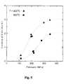
- the graph in FIG. 5presents how solubility of GaN in supercritical ammonia-containing solution depends on pressure, for temperature 400° C. and 500° C.
- the solubilityis defined as the molar percentage: S m ⁇ [GaN solution :(KNH 2 +NH 3 )] ⁇ 100%.
- S mshould be a smooth function of only three parameters: temperature, pressure, and molar ratio of the mineralizer (i.e.
- S mS m (T, p, x)).
- Small changes of S mcan be expressed as: ⁇ S m ⁇ ( ⁇ S m / ⁇ T )
- the partial differentialsare called “coefficients” (e.g. ( ⁇ S m / ⁇ T)
- the solubilityis a decereasing function of temperature and an increasing function of pressure.
- the solubilityis a decereasing function of temperature and an increasing function of pressure.
- Negative temperature coefficient of solubilitymeans that in the presence of a temperature gradient the chemical transport of gallium-containing nitride occurs from lower temperature dissolution zone to higher temperature crystallization zone.
- the deposited nitride monocrystalmay contain Group I elements in a concentration greater that 0.1 ppm since Group I element ions are present in the supercritical ammonia-containing solution.
- no halogensare intentionally introduced into the supercritical ammonia-containing solution, although some halides may be brought into the solution with starting materials, in particular with a feedstock in the form of HVPE gallium-containing nitride wafers, as well as with seeds obtained by the same method, as the seeds may be slightly dissolved in the early stage of the process.
- intentional replacing of 0.05 to 0.50 Ga by Almay be achieved, because of great similarity of the crystal lattice constants of the GaN and AlN, by a respective modification of the composition of the supercritical solution.
- the bulk nitride crystals obtained by the process according to the present inventionmay be also intentionally doped with donor dopants (such as Si) and/or acceptor dopants (such a Mg, Zn) or else magnetic dopants (such as Mn and Cr) in concentrations of 10 17 to 10 21 /cm 3 .
- donor dopantssuch as Si
- acceptor dopantssuch as Mg, Zn
- magnetic dopantssuch as Mn and Cr
- the bulk monocrystals obtainedhave surface dislocation density typically lower than 10 6 /cm 2 , preferably lower than 10 5 /cm 2 and most preferably lower than 10 4 /cm 2 .
- What is typical for the process according to the present inventionis that even if monocrystalline seed of a relatively poor surface quality (with dislocation desity higher than 10 7 /cm 2 ) is used, the obtained bulk gallium-containing nitride layer may have the surface quality significantly improved, so that surface dislocation density value drops to 10 4 /cm 2 .
- FIG. 3 and FIG. 4The apparatus is schematically presented in FIG. 3 and FIG. 4 , although it has to be noticed that the inventive process can be realized in pressurized reaction vessels of different constructions as long as the principles outlined in the specification and the claims are adhered to.
- the main part of the apparatusis an autoclave 1 used for bringing the solvent into a supercritical state.
- the autoclaveis equipped with the installation 2 , which enhance chemical transport in the supercritical solution within the autoclave 1 .
- the autoclave 1is situated in the chamber 3 of the furnace 4 , equipped with heating units 5 and cooling means 6 . Position of the autoclave 1 within the chamber 3 is secured by a screw blocking device 7 .
- the furnace 4is embedded in the bed 8 and secured with steel tapes 2 tightly wound around the furnace 4 and the bed 8 .
- the bed 8 with the furnace 4is pivotally mounted on the supporting base 10 and secured in the desired position by means of a pin securing device 11 .
- the convective flow in the autoclave 1 placed in the furnace 4is established by means of the installation 2 in the form of a horizontal baffle 12 of a size corresponding to 70% of horizontal cross section area of the autoclave 1 .
- the baffle 12separates the dissolution zone 13 from the crystallization zone 14 .
- the horizontal baffle 12is located approximately in the middle of the autoclave 1 in terms of longitudinal dimension. Temperature values in individual zones of the autoclave 1 within a range between 100° C. and 800° C. are controlled by setting up respective temperature for the furnace 4 by a control unit 15 .
- the dissolution zone 13 corresponding to low temperature zone of the furnace 4is situated above the horizontal baffle(s) 12 .
- the feedstock 16is placed in the dissolution zone 13 and the quantity of the feedstock 16 is such that its volume does not exceed 50% of volume of the dissolution zone 13 .
- the total volume of the crucibleshould not exceed 80% of volume of the dissolution zone 13 and the amount of metallic gallium feedstock 16 should match the former requirement (50% of the dissolution zone volume).
- the crystallization zone 14corresponds to high temperature zone of the furnace 4 and is situated below the separating baffle(s) 12 .
- the seed 17is located and the specific position in which the seed 17 is placed is below crossing of up-stream convective flow and down-stream convective flow, but still above the bottom of the crystallization zone 14 .
- the separating baffle(s) 12is/are positioned within the zone of cooling means 6 . As the result of cooling the baffle 12 region, the temperature difference between the dissolution zone 13 and the crystallization zone 14 may be controlled.
- At the level of bottom of the crystallization zone 14there is another cooling device 18 used in order to cool down the zone after the process is over, so that the dissolution of the grown crystal(s) during the cooling stage after the process is remarkably reduced.
- the bulk monocrystals of gallium-containing nitride obtained by the process according to the present inventionmay be used as substrates for opto-electronic semiconductor devices based on nitrides, in particular for laser diodes.
- Dissolution zone of an 84 cm 3 high-pressure autoclave( FIG. 4 ) was charged with 6.0 g of feedstock in the form of gallium nitride wafers obtained by HVPE method, each of 200 ⁇ m thickness as well as 0.27 g of 6N metallic gallium, and 0.5 g of GaN seeds obtained also by HVPE method were placed in the crystallization zone of the same autoclave. Then 9.8 g of 5N sodium azide and 39 g of 5N ammonia were placed in the autoclave. The autoclave was closed, put into the chamber of a furnace and heated up to 300° C. This temperature was maintained inside the autoclave for the next two days.
- the azidewas decomposed and the ammonobasic solvent was produced, which enabled complete dissolution of metallic gallium.
- the temperature in the dissolution zone of the autoclavewas increased to 400° C., while the temperature of the crystallization zone was increased to 500° C.
- This temperature distribution inside the autoclavewas maintained for another 14 days ( FIG. 6 ).
- the expected pressure within the autoclaveis ca. 230 MPa.
- the real pressureturned out to be ca. 330 MPa and the observed increment was the effect of gaseous nitrogen, produced during decomposition of the azide.
- Dissolution zone of an 84 cm 3 high-pressure autoclave( FIG. 4 ) was charged with 6.0 g of feedstock in the form of gallium nitride wafers obtained by HVPE method, each of 200 ⁇ m thickness as well as 1.05 g of 6N metallic gallium, and 0.7 g of GaN seeds obtained also by HVPE method were placed in the crystallization zone of the same autoclave. Then 4.9 g of 5N sodium azide, 2.9 g of 4N metallic potassium and 39 g of 5N ammonia were placed in the autoclave. The autoclave was closed, put into the chamber of a furnace and heated up to 300° C. This temperature was maintained inside the autoclave for the next two days.
- the azidewas decomposed and the ammonobasic solvent was produced, which enabled complete dissolution of metallic gallium.
- the temperature in the autoclavewas increased to 500° C. for one day.
- the temperature of the dissolution zonewas decreased to 450° C.
- the temperature of the crystallization zonewas increased to 550° C.
- This temperature distribution inside the autoclavewas maintained for another 7 days ( FIG. 7 ).
- the expected pressure within the autoclaveis ca. 260 MPa.
- the real pressureturned out to be ca. 310 MPa and the observed increment was the effect of gaseous nitrogen, produced during decomposition of the azide.
- Dissolution zone of an 84 cm 3 high-pressure autoclave( FIG. 4 ) was charged with 8.0 g of feedstock in the form of 6N metallic gallium, and 0.5 g of GaN seeds obtained also by HVPE method, each of ca. 250 ⁇ m thickness, were placed in the crystallization zone of the same autoclave. Then 4.9 g of 5N sodium azide and 38 g of 5N ammonia were placed in the autoclave. The autoclave was closed and put into the chamber of a furnace. The temperature in the dissolution zone of the autoclave was increased to 500° C. by slow heating (0.35° C./min), while the temperature in the crystallization zone was maintained at the level of 300° C. The target temperature of 500° C.
- ELOG structuresseeds possessing surfaces susceptible to the lateral overgrowth
- Dissolution zone of an 84 cm 3 high-pressure autoclave( FIG. 4 ) was charged with 0.5 g of feedstock in the form of aluminum nitride tablet as well as 0.28 g of 6N metallic gallium, and 1.6 g of GaN seeds obtained also by HVPE method were placed in the crystallization zone of the same autoclave. Then 9.2 g of 4N sodium azide and 36.6 g of 5N ammonia were placed in the autoclave. The autoclave was closed, put into the chamber of a furnace and the temperature inside the autoclave was increased to 325° C. (in the crystallization zone) and to 275° C. (in the dissolution zone) for one day.
- the azidewas decomposed and ammonobasic solvent was produced, which enabled total dissolution of metallic gallium.
- the temperature of the dissolution zonewas then increased to 400° C., while the temperature of the crystallization zone was increased to 500° C. ( FIG. 9 ).
- the temperaturewas very slowly (at ca. 2° C./h) increased to 450° C. and 550° C. in the dissolution and crystallization zones respectively.
- the expected pressure within the autoclaveis ca. 260 MPa.
- the real pressureturned out to be ca. 360 MPa and the observed increment was the effect of gaseous nitrogen, produced during decomposition of the azide.
- the autoclavewas maintained for another 2 days ( FIG. 9 ).
- FIG. 10shows a sectional view of a ridge type UV laser diode 100 having an active layer of Al x Ga 1-x N (0 ⁇ x ⁇ 0.7) multi-quantum well (MQW) structure, which is formed on the inventive substrate 101 of GaN having a defect density of 10 6 /cm 2 made by the method of crystallization from supercritical solution disclosed in the Polish Patent Application No. P-347918.
- MQWmulti-quantum well
- the following layersare formed on the substrate 101 by MOCVD method: a buffer layer 102 made of 4 ⁇ m Al 0.05 Ga 0.95 N, an n-type contact layer 103 of 5 ⁇ m Al 0.05 Ga 0.95 N doped with Si, a crack-preventing layer 104 of 0.15 ⁇ m In 0.06 Ga 0.94 N doped with Si, formed at 800° C., an n-type clad layer 105 of super lattice comprising 100 layers of 2.5 ⁇ m (25 ⁇ ) Al 0.05 Ga 0.95 N doped with Si of 5 ⁇ 10 18 /cm 3 and 100 layers of 2.5 nm un-doped Al 0.1 Ga 0.9 N and an n-type optical guide layer 106 of 0.15 ⁇ m un-doped Al 0.15 Ga 0.85 N. Any other layers than the n-type clad layer 105 may be omitted depending on the device characteristics.
- an active layer 107is formed, which comprises multi-quantum well structure made by combination of 4.5 nm un-doped GaN well-layer and 10 nm Al 0.15 Ga 0.85 N barrier layer, wherein the well layer may be un-doped while the barrier layer may be doped with n-type dopant such as Si of 10 17 to 10 19 /cm 3 .
- the most upside barrier layermay be un-doped to prevent Mg-diffusion from the next layer, i.e. p-type carrier confining layer 108 containing p-type dopant such as Mg.
- the p-type nitride semiconductoris formed, comprising a p-type electron confirming layer 108 of 10 nm p-Al 0.3 Ga 0.7 N doped with Mg of 1 ⁇ 10 19 /cm 3 , a p-type optical guide layer 109 of 0.15 ⁇ m Al 0.04 Ga 0.96 N doped with Mg, a p-type super-lattice clad layer 110 of 90 layers (0.45 ⁇ m) of 2.5 nm p-Al 0.1 Ga 0.9 N/2.5 nm Al 0.05 Ga 0.95 N (at least one of them doped with Mg) and a p-type contact layer 111 of 15 nm p-GaN doped with Mg of 10 21 /cm 3 . Any other layers than the p-type clad layer 110 may be omitted depending on the device characteristics.
- the laser diodeis provided with a ridge strip made by etching in a manner that both side etched optical guide layer 109 is up to 0.1 ⁇ m in thickness.
- the described deviceis also provided with a strip-like p-electrode 120 of Ni/Au, a strip-like n-electrode 121 of Ti/Al, a protective layer 162 of ZrO 2 , a dielectric multi-layer 164 of SiO 2 and TiO 2 , and pad electrodes 122 and 123 of Ni—Ti—Au.
- High-pressure autoclave 1( FIG. 3 and FIG. 4 ), having the inner diameter of 40 mm, length equal to 480 mm and volume of 600 cm 3 , was charged with 53.0 g of 6N metallic gallium in the dissolution zone 13 , and 8 seeds of the diameter of 1 inch and mass of 2.0 g each in the form of GaN obtained by HVPE method were placed in the crystallization zone 14 of the same autoclave. Then 46.2 g of 5N sodium azide, 23.5 g of 5N potassium azide and 255 g of 5N ammonia were placed in the autoclave 1 . The temperature in the dissolution zone of the autoclave was increased to 450° C.
- the real pressureturned out to be ca. 320 MPa and the observed increment was the effect of gaseous nitrogen, produced during decomposition of the azide.
- partial dissolution of the feedstocki.e. polycrystalline GaN
- growth of monocrystalline gallium nitride layers on both sides of each seed in the crystallization zone 14was observed.
- the total thickness of the re-crystallized layerswas ca. 5 mm.
- the thus obtained monocrystalwas subject to the following processing, so as to obtain substrates for epitaxy:
Landscapes
- Chemical & Material Sciences (AREA)
- Engineering & Computer Science (AREA)
- Crystallography & Structural Chemistry (AREA)
- Materials Engineering (AREA)
- Metallurgy (AREA)
- Organic Chemistry (AREA)
- Inorganic Chemistry (AREA)
- Crystals, And After-Treatments Of Crystals (AREA)
- Semiconductor Lasers (AREA)
Abstract
Description
- The invention relates to new improvements in a process for obtaining of bulk monocrystalline gallium-containing nitride, as well as in bulk Group XIII element nitride monocrystals and use thereof (numbering of the Groups is given according to the IUPAC convention of 1989 throughout this application). The improvements relate in general to a process for crystal growth in the environment of supercritical ammonia-containing solution and the crystals obtained in such a process. The improved process and the improved bulk monocrystals are mainly intended for variety of nitride-based semiconductor products such as various opto-electronic devices. The present invention relates also to a mineralizer used for supercritical ammonia-containing solution.
- Known opto-electronic devices are based on use of Group XIII element nitrides such as AlN, GaN and InN and mixed Group XIII element nitrides containing two or three Group XIII elements. Such nitrides have thus far been manufactured on sapphire or silicon-carbide substrates, differing from the thereafter deposited nitride layers (i.e. heteroepitaxy).
- The two most commonly used methods, i.e. Metallo-Organic Chemical Vapor Deposition (MOCVD) method and Halide Vapor Phase Epitaxy (HVPE) [“Optical patterning of GaN films” M. K. Kelly, O. Ambacher, Appl. Phys. Lett. 69 (12)(1996) and “Fabrication of thin-film InGaN light-emitting diode membranes” W. S. Wrong, T. Sands, Appl. Phys. Lett. 75 (10) (1999)], based on depositing nitrides from the gaseous phase, have many technological drawbacks that make it impossible to obtain bulk monocrystalline layers of desired nitrides of a sufficiently good quality. The nitride monocrystals grown according to those methods have a high surface dislocation density, usually about 107/cm2to 109/cm2. Besides, due to distortion caused by epitaxial growth on hetero-substrates, for example on sapphire, the HVPE substrates have tilted crystal axes, which is detrimental to the quality of the opto-electronic devices produced on such substrates.
- Due to significant differences in chemical, physical, crystallographic and electrical properties of substrates such as sapphire or silicon carbide and semiconductor nitride layers deposited thereon by hetero-epitaxy, big technological effort is needed to advance progress in opto-electronics.
- Certain decrease of density of dislocations and other defects could be attained by using the Epitaxial Lateral Overgrowth (ELOG) method. In this method, a nitride layer is first grown on the sapphire substrate, and then SiO2is deposited in the form of strips or grids. Next, such a substrate may be used for lateral nitride growing, reducing the defects density to about 107/cm2.
- On the other hand growth of bulk crystals of gallium nitride and other nitrides of Group XIII elements is also extremely difficult Standard methods of crystallization from melt and sublimation methods are not applicable because of decomposition of the nitrides into metals and N2. In the High Nitrogen Pressure (HNP) method [,,Prospects for high-pressure crystal growth of III-V nitrides” S. Porowski et al., Inst. Phys. Conf. Series, 137, 369 (1998)] decomposition is inhibited by applying a nitrogen atmosphere under high pressure. Growth of crystals is carried out in melted gallium, i.e. in the liquid phase, resulting in production of GaN platelets about 10 mm in size. Sufficient solubility of nitrogen in gallium requires temperatures of about 1500° C. and nitrogen pressures of the order of 1500 MPa.
- Supercritical ammonia was proposed to lower the temperature and decrease the pressure during the nitride crystals growth process. It was proven in particular that it is possible to obtain crystalline gallium nitride by synthesis from gallium and ammonia, provided that the latter contains Group I element amides (KNH2or LiNH2). The processes were conducted at temperatures of up to 550° C. and
pressure 500 MPa, yielding crystals of about 5 μm in size [,,AMMONO method of BN, AlN, and GaN synthesis and crystal growth” R. Dwiliński et al., Proc. EGW-3, Warsaw, Jun. 22-24, 1998, MRS Internet Journal of Nitride Semiconductor Research, http://nsr.mij.mrs.org/3/25]. - Use of supercritical ammonia also allowed recrystallization of gallium nitride within the feedstock comprising finely crystalline GaN [,,Crystal Growth of gallium nitride in supercritical ammonia” J. W. Kolis et al., J. Cryst. Growth 222, 431-434 (2001)]. Recrystallization was made possible by introduction of amide (KNH2) into supercritical ammonia, along with a small quantity of a halogen (KI). Processes conducted at 400° C. and 340 MPa gave GaN crystals about 0.5 mm in size. However, no chemical transport processes were observed in the supercritical solution, in particular no growth on seeds.
- The ammonobasic method for preparing gallium-containing nitride crystals has recently been disclosed in WO 02/101120. The method allows production of gallium-containing nitride monocrystals crystallized on at least one crystallization seed in the presence of a Group I element-containing compound in a supercritical ammonia-containing solution. As feedstock for growth of desired crystals, gallium-containing nitrides are used. The thus obtained gallium-containing nitride bulk monocrystals have surface dislocation density lower than surface dislocation density of seeds used in the process. The bulk monocrystals have sufficient size and regular shape enhancing industrial use of the crystals—among others—as substrates for epitaxy in opto-electronic devices. The major advantage of the discussed method is that it has enabled to lower dislocation density in the thus grown GaN monocrystal layers to less than 106/cm2. Besides, the bulk nitride monocrystals obtained by that method have high resistivity (in the case of GaN monocrystals within a range of several Ω·cm) and good crystalline quality, as demonstrated by a low value of FWHM of the X-ray rocking curve from (0002) plane—less then 60 arcsec for a Cu K α1 beam.
- Ammonothermal method for growing gallium nitride crystals on seeds is described in French
patent application FR 2 796 657 A. In view of the experiments disclosed in WO 02/101120 and the experience based thereon, according to the teaching contained in the French application, neither temperature distribution of the process can be successfully selected for the effective crystal growth nor the seeds can be effectively protected against dissolution in supercritical solvent without intensive research being done. Moreover, the arrangement of feedstock and seeds, disclosed in theFrench application FR 2 796 657 A, is disadvantageous. - Further research studies have proven that the crystalline quality of the optically active nitride layers depends also on other factors, such as presence of heteroatoms in the Group XIII element nitrides lattice. Various sources of such heteroatoms built-in the crystalline structure of the nitrides have been considered and examined.
- In a number of tests it has been proven that although the high grade reagents have been used in the process according to WO 02/101120 a content of the undesired impurities fluctuates from one charge of the reaction vessel to another and cannot be easily controlled.
- It has further been proven that in spite of use of the various technical measures such as use of a glove box for introducing solid reagents to the reaction vessels, oxygen has turned out to be one of the most troublesome impurities. There are difficulties in controlling its content in the environment of the ammonobasic nitride-crystals growth process, mainly due to the fact that oxygen may be introduced as an impurity contained in the mineralizer necessary to obtain a supercritical ammonia-containing solution.
- It is thus the main aim of the present invention to improve the above discussed ammonobasic method for preparing gallium-containing nitride crystals in the presence of mineralizer in a supercritical ammonia-containing solution by elimination of certain impurities from the crystallization solution and obtained nitride crystals, and thus to provide an improved product for use in opto-electronics and electronics. It is a further aim of the present invention to provide a mineralizer suitable for use in the ammonobasic method for preparing gallium containing nitride crystals. These aims have been achieved by developing technical solutions according to the invention as defined in the appended claims.
- A process for obtaining a bulk gallium-containing nitride monocrystal according to the present invention is carried out as defined in the
independent claims - A bulk gallium-containing nitride monocrystal obtained by the process according to the present invention is covered as stated in claim21 and respective claims dependent on claim21.
- Use of a bulk gallium-containing nitride monocrystals obtained by the process according to the present invention is indicated in the claims22 to24.
- Finally, mineralizer used for supercritical ammonia-containing solution is defined in the appended claims25 to30.
- Process for obtaining a bulk gallium-containing nitride monocrystals from supercritical ammonia-containing solution in the presence of a mineralizer, according to the present invention is characterized in that in a pressurized reaction vessel—using ammonia as solvent and Group I element azides and optionally Group II element azides as mineralizer, a supercritical ammonia-containing solution including Group I and optionally Group II element ions is first obtained to dissolve next a gallium-containing feedstock at dissolution temperature and/or dissolution pressure and then the desired gallium-containing nitride is crystallized from the supercritical solution on the surface of at least one seed at the crystallization temperature and/or crystallization pressure, wherein the crystallization temperature and/or crystallization pressure is selected according to the temperature coefficient of solubility and pressure coefficient of solubility of the desired gallium-containing nitride to be crystallized.
- Process for obtaining bulk gallium-containing nitride monocrystals from supercritical ammonia-containing solution in the presence of Group I and optionally Group II element-containing mineralizer, according to the present invention is characterized in that when gallium-containing nitride has a negative temperature coefficient of solubility and a positive pressure coefficient of solubility in supercritical ammonia-containing solution, in the presence of Group I and optionally Group II element-containing mineralizer, in a pressurized reaction vessel—using Group I element azides and optionally Group II element azides as mineralizers—supercritical ammonia-containing solution including Group I and optionally Group II element ions is first obtained to dissolve next a gallium-containing feedstock at dissolution temperature and/or dissolution pressure and then gallium-containing nitride is crystallized from the supercritical solution on the surface of at least one seed by means of bringing the temperature to crystallization temperature and/or the pressure to crystallization pressure, the crystallization temperature being higher than the dissolution temperature and/or the crystallization pressure being lower than the dissolution pressure at least at the crystallization zone of the pressurized reaction vessel, where the seed is placed—so that super-saturation of the supercritical solution with respect to the seed is achieved—and then the super-saturation of the supercritical solution is maintained at the level at which spontaneous crystallization of the nitride may be neglected, while crystallization of the desired gallium-containing nitride is carried out on the seed.
- In the process according to the invention the gaseous nitrogen, produced during the decomposition of the azide, is preferably at least partially evacuated from the system before the re-crystallization step is started.
- In one preferred embodiment of the above process as a gallium-containing nitride—the nitride having a general formula AlxGa1-xN, where 0≦x<1 is being crystallized.
- In the above process the azide mineralizers selected from the group consisting of LiN3, NaN3, KN3, CsN3and mixtures thereof are used.
- The mineralizer used contains at least one compound selected from the group consisting of LiN3, NaN3, KN3and CsN3. In particular, the mineralizer may contain NaN3and KN3or NaN3and LiN3or else KN3and LiN3mixed in arbitrary molar ratio. The mineralizer may also contain Group I and optionally Group II element-containing compound(s) other than azides.
- Group I element azides are introduced into the system in a molar ratio of azides to ammonia ranging from 1:200 to 1:2.
- In the process according to the invention a seed crystal with at least one crystalline layer of Group XIII element nitride, preferably gallium-containing nitride, having a dislocation density less than 107/cm2is used.
- In the process according to the invention a structure having a number of surfaces spaced adequately far from each other, arranged on a primary substrate and susceptible to the lateral overgrowth of crystalline nitrides may be used as a seed.
- As the primary substrate of the seed used in the process according to the present invention a crystalline nitride of Group XIII elements, preferably gallium nitride—GaN, is used.
- Alternatively, the seed may contain as the primary substrate a crystalline material such as sapphire, spinel, ZnO, SiC or Si, wherein the primary substrate made of the material reacting with a supercritical ammonia-containing solution is covered with a protective layer, preferably made of a nitride containing Group XIII elements or metallic silver, prior to formation of a monocrystalline nitride layer.
- Preferably, in the process according to the invention some surfaces of the seeds are covered with a mask layer prior to formation of a monocrystalline nitride layer.
- The present process allows to obtain a monocrystalline nitride layer having the same or better quality as it gets thicker.
- Preferably, in the process according to the invention bulk nitride monocrystals obtained consist essentially of gallium nitride—GaN. The bulk nitride monocrystals obtained may contain any of the following elements: Ni, Cr, Co, Ti, Fe, Al, Ag, Mo, W, Si and Mn.
- The present invention relates also to a bulk nitride monocrystals obtained by the above process.
- The thus obtained bulk nitride monocrystals are suitable for use as substrates for epitaxy and as templates, i.e. bulk nitride monocrystals having surface modified by epitaxial monocrystalline layer(s) of the same or different Group XIII element nitride deposited by MOCVD or HVPE or else MBE, optionally doped with various dopants.
- Mineralizer used for supercritical ammonia-containing solution according to the invention comprises at least one compound selected from the group consisting of LiN3, NaN3, KN3, and CsN3.
- Preferably, it contains NaN3and KN3or NaN3and LiN3, or KN3and LiN3in arbitrary molar ratio of NaN3to KN3, NaN3to LiN3and KN3to LiN3.
- Alternatively, it may contain NaN3, KN3and LiN3in arbitrary molar ratio of NaN3to KN3and LiN3.
- Mineralizer according to the present invention may also further contain Group I and optionally Group II element-containing compound(s) other than azides and/or Group I element, and/or Group II element.
- The main advantage of the present process according to the invention is that in the product obtained by the process certain uncontrolled impurities can be eliminated. Among such impurities are those introduced to the reaction solution with starting materials, the most troublesome being hygroscopic reagents bringing in oxygen in the form of absorbed water. Significant degree of elimination of oxygen from the bulk nitride monocrystals obtainable by the process according to the present invention is particularly desired when n-type electrically conductive layers are to be produced by using Si dopants.
- In this respect the present invention provides successfully an improved product for use in opto-electronics and electronics.
- Furthermore, the bulk gallium-containing nitride monocrystals obtained by the process according to the invention have at least one surface suitable for epitaxial growth of semiconducting nitride layers without any additional pre-treatment, the surface being a C-plane or more preferably non-polar A-plane or M-plane.
- The big advantage of the process according to the present invention is such, that the dislocation density of the thus obtained bulk monocrystals may be orders of magnitude lower than the dislocation density of the seed used.
- The accompanying drawings illustrate the present invention and
FIG. 1 shows the change of temperature in time inside the autoclave at a constant pressure and illustrates the relation between the change of the temperature and dissolution and crystallization steps in the process according to the present invention,FIG. 2 presents the change of pressure in time inside the autoclave at constant temperature and illustrates the relation between the change of the pressure and dissolution and crystallization steps in the process according to the present invention,FIG. 3 shows a schematic axial cross section of an autoclave and a set of furnaces, as used to run the process according to the present invention,FIG. 4 presents a schematic perspective drawing of an apparatus used to run the process according to the present invention,FIG. 5 shows the dependence of GaN solubility in supercritical ammonia containing potassium amide (in the molar ratio of KNH2:NH3=0.07) on pressure at temperature T=400° C. and T=500° C.,FIG. 6 shows the change of temperature in time inside the autoclave in Example 1,FIG. 7 presents the change of pressure in time inside the autoclave in Example 2,FIG. 8 presents the change of temperature in time in the autoclave in Example 3,FIG. 9 presents the change of temperature in time in the autoclave in Example 6,FIG. 10 shows a cross-section of a semiconductor UV laser diode/GaN substrate andFIG. 11 presents the change of temperature in time in the autoclave in Example 8. - In the present invention the following definitions apply:
- Group XIII element nitride means a nitride of Group XIII elements, i.e. aluminum, gallium and indium either alone or in any combination. Gallium-containing nitride is the most preferred such nitride.
- Gallium-containing nitride means a nitride of gallium and optionally other element(s) of Group XIII. It includes, but is not restricted to, the binary compound GaN, ternary compounds such as AlGaN, InGaN, and also quaternary compound AlInGaN—AlGaN being the most preferred one, where the ratio of other elements of Group XIII to Ga can vary in a wide range.
- Bulk monocrystal of gallium-containing nitride means a monocrystal—especially for use as a substrate for epitaxy—made of gallium-containing nitride, from which opto-electronic devices such as LED or LD can be formed by epitaxial methods, such as MOCVD and HVPE.
- C-, A- or M-plane refers to C-, A- or M-plane surfaces of hexagonal Group XIII element nitride crystals.
- Precursor of gallium-containing nitride is a substance or a mixture of substances containing at least gallium and optionally containing also Group I elements, Group II elements, Group XIII element(s), nitrogen and/or hydrogen; it may also be metallic gallium or alloys of gallium as well as gallium hydrides, amides, imides, amido-imides and azides that can form gallium compounds soluble in supercritical ammonia-containing solvent.
- Gallium-containing feedstock is a gallium-containing nitride or Group XIII element nitride or their precursors. As a feedstock, GaN obtained by various methods may be used, among others by flux methods, HNP method, HVPE methods. Moreover, polycrystalline GaN obtained by reaction of metallic gallium with supercritical ammonia-containing solution may be used.
- Supercritical ammonia-containing solution means a fluid in a supercritical state, consisting essentially of ammonia and one or more Group I and optionally Group II element ions, used to dissolve a gallium-containing feedstock.
- Mineralizer is generally a substance introducing into the supercritical ammonia-containing solution one or more Group I and optionally Group II element ions, affecting dissolution of a feedstock and gallium containing nitride.
- Dissolution of gallium-containing feedstock means either reversible or irreversible process of forming out of said feedstock gallium compounds soluble in the supercritical solvent, for example gallium-complex compounds. Gallium complex compounds are complex chemical compounds, in which a gallium atom is a coordination center surrounded by ligands, such as ammonia molecules or its derivatives, like NH2−, NH2−, etc.
- Supercritical solution is used when referring to the supercritical solvent when it contains Group XIII element(s), in particular gallium—in a soluble form, originating from the dissolution of a Group XIII element(s)-containing feedstock, in particular gallium.
- Solubility: According to our experience at sufficiently high temperature and pressure equilibrium state may be established between the solid state such as gallium-containing nitride and the supercritical solution. For this reason solubility of gallium-containing nitride may be defined as the equilibrium concentration of soluble gallium compounds, as obtained in the above defined dissolution process. In the process according to the present invention the equilibrium concentration, i.e. solubility, may be controlled by changing composition of the solution, temperature and/or pressure.
- Negative temperature coefficient of solubility means that the solubility of the respective compound is a monotonically decreasing function of temperature if all other parameters are kept constant. Similarly, positive pressure coefficient of solubility means that, if all other parameters are kept constant, the solubility is a monotonically increasing function of pressure. In our research we have shown that the solubility of gallium-containing nitride in supercritical ammonia-containing solvent possesses a negative temperature coefficient and a positive pressure coefficient in temperature ranging at least from 300° C. to 550° C. and pressure from 100 to 550 MPa. This means that in accordance to
FIG. 1 , after dissolution of feedstock in an autoclave kept for 8 days at thetemperature 400° C. (i.e. after dissolution step) re-crystallization of gallium nitride may be achieved by increasing the temperature inside the furnace to 500° C., while keeping constant pressure of 200 MPa (crystallization step). On the other hand, as shown inFIG. 2 , after dissolution of a feedstock at increased pressure in an autoclave kept for 2 days at the level of 350 MPa (i.e. after dissolution step), re-crystallization of gallium nitride is achieved by means of reducing the pressure to 200 MPa while keeping constant temperature of 500° C. (crystallization step). - Super-saturation: if concentration of soluble gallium compounds in supercritical ammonia-containing solution is higher then the solubility of gallium-containing nitride at given physical and chemical conditions, then super-saturation of the supercritical solution with respect to gallium-containing nitride may be defined as the difference between said concentration and solubility. In the case of dissolution of gallium-containing nitride in a closed system, such a super-saturation can be achieved by increasing temperature and/or decreasing pressure.
- Chemical transport of gallium-containing nitride in the supercritical solution means a continuous process involving dissolution of a gallium-containing feedstock in the supercritical solution, circulation of the soluble gallium compounds within the solution and crystallization of gallium-containing nitride from the super-saturated supercritical solution. Generally, chemical transport may be caused by temperature difference, pressure difference, concentration difference, or other chemical or physical differences between the dissolved feedstock and the crystallization product. According to the present invention a bulk monocrystalline gallium-containing nitride may be obtained in effect of chemical transport between the dissolution and crystallization zones of the autoclave, established by means of temperature difference between the two zones, whereas the temperature of crystallization zone should be higher than the temperature of dissolution zone.
- Seed, as it has already been mentioned, is crucial for obtaining a desired bulk gallium-containing nitride monocrystals in a process according to the present invention. In view of the fact that the quality of the seed is crucial for the crystalline quality of the bulk gallium-containing nitride monocrystals obtained by the process according to the present invention, the seed selected for the process should have possibly high quality. Various structures or wafers having a modified surface can also be used. For example a structure having a number of surfaces spaced adequately far from each other, arranged on a primary substrate and susceptible to the lateral overgrowth of crystalline nitrides may be used as seeds. Moreover, a seed having a homoepitaxial surface, exhibiting n-type electric conductivity, for example doped with Si, may be used. Such seeds can be produced using processes for gallium-containing nitride crystal growth from gaseous phase, such as HVPE or MOCVD, or else MBE. Doping with Si during the growth process at the level of 1016to 1021/cm2ensures n-type electric conductivity. Moreover, a composite seed may be used and in such seed directly on a primary substrate or on a buffer layer made for example of AlN—a layer made of GaN doped with Si may be deposited.
- Spontaneous crystallization from the super-saturated supercritical solution means any undesired process of nucleation and growth of the gallium-containing nitride crystals taking place at any site within the autoclave except at the surface of the seed crystal(s). Spontaneous crystallization also comprises nucleation and growth on the surface of the seed crystal(s) if the grown crystal has an orientation different from that of the seed.
- Selective crystallization on a seed means a process of crystallization taking place on the surface of the seed, carried out without spontaneous crystallization or with spontaneous crystallization taking place to a negligible extend. This is a process indispensable for achieving the aim of the present invention, i.e. obtaining a bulk gallium-containing nitride monocrystal and at the same time an essential element of the present invention.
- Temperature and pressure of the reaction: In the practical examples presented in the present specification temperature measurements inside the autoclave have been performed when the autoclave was empty, i.e. without the supercritical ammonia-containing solution. Thus, the temperature values cited in the examples are not the actual temperature values of the process carried out in the supercritical state. Pressure was measured directly or calculated on the basis of physical and chemical data for supercritical ammonia at selected process temperature and the volume of the autoclave. In the process according to the present invention increase of pressure caused by decomposition of azide mineralized was taken into consideration as well.
- Autoclave means a closed and pressurized reaction vessel, which has a reaction chamber where the ammonobasic process according to the present invention is carried out.
- As it has been stated earlier, the present process involves dissolution of a gallium-containing feedstock in a supercritical solvent and crystallization of a desired gallium-containing nitride on a surface of a seed crystal, with over-saturation of the supercritical solution with respect to the desired gallium-containing nitride, achieved by means of temperature gradient and/or pressure change.
- The supercritical solution contains ammonia and/or its derivatives, and includes ions of Group I and optionally Group II elements. The specific ions are introduced in the form of azides, such as lithium azide, sodium azide, potassium azide, and cesium azide, or mixtures thereof.
- The feedstock consists essentially of Group XIII element(s)-containing nitrides and/or its precursors, selected from the group including azides, imides, amido-imides, amides, hydrides, Group XIII element(s)-containing metal compounds and alloys, as well as pure metallic elements of Group XIII. Gallium is the preferred Group XIII element.
- Generally, the first variant of the process according to the invention allows to improve crystal growth conditions and to obtain a bulk gallium-containing nitride monocrystals from supercritical ammonia-containing solution in the presence of a mineralizer, in a process of selective crystallization on a seed that can take place in turns of chemical transport in the supercritical solution, containing ammonobasic mineralizers.
- The present process for obtaining a bulk monocrystalline gallium-containing nitride is characterized in that in a pressurized reaction vessel—using ammonia as solvent and Group I element azides and optionally Group II element azides as mineralizer, a supercritical ammonia-containing solution including Group I and optionally Group II element ions is first obtained to dissolve in the next step a gallium-containing feedstock at dissolution temperature and/or dissolution pressure and then the desired gallium-containing nitride is crystallized from the supercritical solution on the surface of at least one seed at the crystallization temperature and/or crystallization pressure, wherein the crystallization temperature and/or crystallization pressure is selected according to the temperature coefficient of solubility and pressure coefficient of solubility of the desired gallium-containing nitride to be crystallized. In this variant of the process according to the invention it is preferred to run the crystallization process from the supercritical solution super-saturated to such extend as to avoid spontaneous crystallization of the desired gallium-containing nitride, that is to obtain crystal growth on the seeds only.
- The second variant of the process according to the present invention is directed to a process for obtaining bulk gallium-containing nitride monocrystals from supercritical ammonia-containing solution in the presence of Group I and optionally Group II element-containing mineralizer, characterized in that when gallium-containing nitride has a negative temperature coefficient of solubility and a positive pressure coefficient of solubility in supercritical ammonia-containing solution, in the presence of Group I and optionally Group II element-containing mineralizer, in a pressurized reaction vessel—using Group I element azides and optionally Group II element azides as mineralizers—supercritical ammonia-containing solution including Group I and optionally Group II element ions is first obtained to dissolve next a gallium-containing feedstock at dissolution temperature and/or dissolution pressure and then gallium-containing nitride is crystallized from the supercritical solution on the surface of at least one seed by means of bringing the temperature to crystallization temperature and/or the pressure to crystallization pressure, the crystallization temperature being higher than the dissolution temperature and/or the crystallization pressure being lower than the dissolution pressure at least at the crystallization zone of the pressurized reaction vessel, where the seed is placed—super-saturation of the supercritical solution with respect to the seed is achieved—and then the super-saturation of the supercritical solution is maintained at the level at which spontaneous crystallization of the nitride may be neglected, crystallization of the desired gallium-containing nitride is carried out on the seed.
- If in the second variant of the process according to the invention two separate zones are created in the autoclave, i.e. the dissolution zone and the crystallization zone, the super-saturation of the solution with respect to the seeds can be controlled by regulating the dissolution and crystallization temperature. The temperature control shall present no technical problem if the process is carried out within the temperature range of 300° C. to 600° C., preferably 400° C. to 550° C. and the temperature difference between the two zones is maintained at the level of ca. 150° C., preferably below ca. 100° C.. The super-saturation control can be also achieved by placing in the autoclave one or more baffles separating the dissolution zone from the crystallization zone and controlling convective mass flow within the autoclave. Besides, when two separate temperature zones are created within the autoclave, super-saturation of the supercritical solution with respect to the seed may be controlled if the gallium-containing feedstock—for example in the form of GaN—placed in the dissolution zone of the autoclave is used, that has much greater total surface area then the total surface area of the seed placed in the crystallization zone of the autoclave.
- Generally, the supercritical solvent should contain mineralizers in order to affect solubility of a feedstock and the solubility can be significantly changed by the presence of Group I and optionally Group II element ions. Lithium, sodium and potassium are preferred as Group I elements, and sodium and potassium are the most preferred.
- It has been proven that in the process according to the present invention use of Group I and optionally Group II element azides is beneficial in various aspects, when the molar ratio of Group I element azides to ammonia ranges from 1:200 to 1:2.
- The Group I and Group II element azides of very high purity in a solid form are available commercially. Moreover, they can be easily purified. Once purified, the azides retain high purity for a relatively long time, as they are non-reactive and almost non-hygroscopic, thus they do not absorb impurities from air. The azides may be stored, manipulated and (in particular) put into an autoclave without such special precautionary measures or equipment (e.g. a glove box), which are indispensable when handling e.g. metallic lithium, sodium or potassium.
- Group I and Group II element azides dissolve in supercritical ammonia-containing solution. The research studies directed to the use of azide mineralizers in processes according to the present invention revealed that under the present process conditions the azide ammonia solution is chemically stable up to certain temperature, at which the azide starts to decompose (in the case of NaN3this is ca. 250° C.). Below this temperature the azide ammonia solution is hardly reactive with respect to feedstock and the azide does not act as the ammonobasic mineralizer. However, when the temperature of the supercritical ammonia-containing solution goes high enough (in the case of NaN3—beyond 300° C.), intensive decomposition of azide ion N3—takes place and molecular nitrogen N2is released. Only at this stage the azide commences to act as mineralizer, and enhances dissolution of the feedstock and crystallization of gallium-containing nitride on the seed. Thus, if the second variant of the process according to the present invention is realized with metallic gallium as the feedstock, the use of azides makes it easier to control super-saturation and the amount of gallium that does not dissolve.
- The main disadvantage of using azides is the extra pressure, originating from the gaseous nitrogen, released during decomposition of azide. The increment of pressure is remarkable and usually undesired, because more durable autoclaves are then needed. However, one can get rid of this effect. There are several ways to do it The one presented below—as an example—should not be construed as limiting. The azide can be first closed in an empty autoclave (or an autoclave filled with an inert gas), together with the other starting materials (feedstock, seeds etc.) and decomposed by heating to the temperature higher than the decomposition temperature of the azide(s) used. The autoclave contains then a mixture, comprising the (undesired) gaseous nitrogen. Then the temperature should be decreased back, below the critical temperature of the mixture, the autoclave should be at least partially evacuated and charged with the solvent (ammonia). Note, that the Group I and optionally Group II elements remaining in the autoclave after decomposition of their azides may have a very high level of purity, hardly available otherwise.
- Although the present process may be used in order to obtain a variety of Group XIII element nitrides, it will be further explained in details with respect to gallium-containing nitride.
- According to the present invention, crystallization of a bulk monocrystal of gallium-containing nitride takes place in an autoclave, at temperature from 100° C. to 800° C. preferably from of 300° C. to 600° C., most preferably 400° C. to 550° C. and at pressure from 10 MPa to 1000 MPa, preferably from 100 MPa to 550 MPa, while the molar ratio of the above identified azide mineralizers to ammonia ranges from 1:200 to 1:2, preferably from 1:100 to 1:5 and most preferably from 1:20 to 1:8.
- In the preferred embodiment, the present invention relates to a method for obtaining a bulk gallium-containing nitride monocrystal grown in a direction parallel to c-axis of hexagonal lattice of a gallium nitride seed in a supercritical ammonia-containing solution with gallium-complex compounds in the Ga:NH3molar ratio of more than 1:50.
- According to the present invention a bulk monocrystal of gallium-containing nitride is crystallized on a surface of the seed crystal.
- The seed crystals for crystallization of a gallium-containing nitride by means of a process according to the invention are preferably of the same composition as the desired nitride to be crystallized and such seeds can be obtained by a number of known methods, described in details in literature. Various seed crystals may be used, both homo-seeds and hetero-seeds. Generally, a seed crystal consists of gallium-containing nitride (homo-seed) or at least contains a layer of such a nitride (hetero-seed). For example, gallium nitride crystals may be obtained in effect of spontaneous crystallization from the supercritical ammonia-containing solution. Suitable seed crystals may be obtained by methods of synthesis of GaN based on heteroepitaxial deposition, involving halogens in gaseous phase (HVPE). This method is suitable for reproducible manufacturing of big size seed crystals, having even ca. 5 cm in diameter. Such crystals are available from a number of sources, among others they are produced by NICHIA, ATMI, TDI, SUMITOMO and other manufacturers. Seed crystals can be also obtained by HNP method, under which growth of GaN crystals occurs spontaneously in molten gallium under a high pressure nitrogen atmosphere. Recently the paper “Growth of bulk GaN single crystals by the pressure-controlled solution growth method” by T. Inoue, Y. Seki, O. Oda, S. Kurai, Y. Yamada and T. Taguchi has been published in J. Cryst. Growth 229, 35-40 (2001). The authors described a method for producing GaN, similar to HNP method. In their method the crystal growth is initiated by a slow increase of nitrogen pressure and simultaneously maintaining uniform temperature and not by generating a temperature difference within a crucible with a molten gallium. It was reported that the method allows growing GaN monocrystals having up to 10 mm in diameter. Another method suitable for obtaining seed crystals involves melting a mixture of sodium azide, metallic gallium and metallic sodium. With increasing temperature sodium azide decomposes and releases atomic nitrogen, which in turns reacts with gallium, forming the desired gallium nitride.
- Preferably, seeds of monocrystalline GaN are used. GaN seeds obtained by HVPE, flux methods and HNP are available. It is also possible to use as seed monocrystalline GaN plates having A plane (1 1 {overscore (2)} 0), M plane (1 {overscore (1)} 0 0), or R plane (1 {overscore (1)} 0 2) cut out of bulk monocrystal obtained from supercritical ammonia-containing solution. Also N-side of C plane (0001) plate may be used as advantageous seed in the process according to the present invention
- As mentioned above, depositing a bulk monocrystal of gallium-containing nitride may include lateral growth of the desired nitride on a variety of surfaces susceptible to such growth, placed on a crystal seed and spaced apart from each other. A primary substrate as described below should be considered to be a particular seed crystal, and various materials can be used to form such a substrate including homo-seed crystals in the form of flat wafers or hetero-seeds on which a buffer gallium-containing nitride layer is needed.
- According to specific embodiments of the process according to the present invention, the dissolution step and crystallization step may be separated one from the other either by consecutive creation of temperature and pressure condition corresponding to dissolution step and crystallization step in single zone reactor or by creation of at least two zones in the autoclave, in which different temperature is prevailing and placing gallium-containing feedstock in the dissolution zone of lower temperature while placing the seeds in the crystallization zone of higher temperature. The temperature difference between the two zones should be controlled to such extent as to ensure chemical transport in supercritical solution between the two zones.
- As mentioned earlier, gallium-containing nitride has a general formula AlxGa1-xN, where 0≦x<1 and it may contain dopants of donor, acceptor or magnetic nature. Ammonia may be used as the supercritical solvent and Group I and optionally Group II element ions should be present in the solution. A feedstock consists essentially of gallium-containing nitride or its precursors, selected from the group consisting of gallium-containing azides, imides, amido-imides, amides, hydrides, and also metallic compounds and alloys, as well as metallic gallium. The seed preferably comprise a crystalline layer of gallium-containing nitride and the layer may be furthermore doped with Si in amount of 1016to 1021/cm3.
- Crystallization of gallium-containing nitride is carried out at temperature ranging from 100° C. to 800° C. and pressure ranging from 10 to 1000 MPa, and the content of Group I and optionally Group II element ions in the supercritical solution is controlled to ensure suitable solubility of the feedstock and of the gallium-containing nitride product. Molar ratio of Group I element ions to ammonia is controlled to range from 1:200 do 1:2.
- As a feedstock preferably gallium-containing nitride is used, since such a feedstock may be reversibly dissolved in the supercritical ammonia-containing solution. However, it is possible to combine the use of the nitride as a feedstock with the use of metallic gallium, that undergoes irreversible dissolution in the supercritical ammonia-containing solution and contributes to the increase of the overall concentration of soluble gallium compounds in the solution. Use of gallium nitride as a particular type of feedstock in combination with metallic gallium allows for precise control of the crystallization process when GaN bulk monocrystals are produced by a process according to the present invention.
- As mentioned above in the process according to the present invention preferably dissolution step and crystallization step are carried out simultaneously (second variant of the process) in separate zones created and spaced apart in the autoclave. In other words, in the autoclave solvent is brought into the supercritical state and in one zone of the autoclave the gallium-containing feedstock is dissolved while in another zone, at temperature higher than in the dissolution zone and/or at pressure lower than in the dissolution zone, crystallization on the seed is carried out, due to a chemical transport between the two zones, which mainly occurs by convection. In such a process the feedstock is maintained in the lower temperature (or higher pressure) zone while the seeds are kept in the higher temperature (or lower pressure) zone. The temperature difference between the two zones is greater than 1° C. and preferably it is ranging from 5° C. to 150° C., most preferably it is kept below 100° C.
- When dissolution and crystallization steps are carried out consecutively, after dissolution of gallium-containing feedstock in the supercritical ammonia-containing solution, there is a transition stage of bringing the solution into higher temperature or lower pressure conditions. In such a case, super-saturation of the supercritical ammonia-containing solution is controlled strictly by temperature control in order to avoid spontaneous crystallization.
- In order to carry out the process according to the present invention, it is preferred to use the apparatus described in details further below, which is also schematically represented in
FIG. 3 andFIG. 4 . - The research studies have shown that the best bulk monocrystalline gallium-containing nitride product obtained by a process according to the present invention had a surface dislocation density below 104/cm2and at the same time its FWHM rocking-curve value for the (0002) plane (for Cu K α1) was below 60 arcsec. Such parameters can guarantee the quality and durability of semiconductor devices made of such crystals as substrates for epitaxial layers. Because of the electric conductivity exhibited by the product, n-type electrode may be placed on the substrate.
- Gallium nitride exhibits good solubility in supercritical ammonia, provided that the latter contains Group I and optionally Group II elements or their compounds, such as KNH2. The graph in
FIG. 5 presents how solubility of GaN in supercritical ammonia-containing solution depends on pressure, fortemperature 400° C. and 500° C. Here the solubility is defined as the molar percentage: Sm≡[GaNsolution:(KNH2+NH3)]×100%. In this example KNH2is used in the molar ratio of KNH2:NH3=0.07. In this case Smshould be a smooth function of only three parameters: temperature, pressure, and molar ratio of the mineralizer (i.e. Sm=Sm(T, p, x)). Small changes of Smcan be expressed as:
ΔSm≈(∂Sm/∂T)|p,xΔT+(∂Sm/∂p)|T,xΔp+(∂Sm/∂x)|T,pΔx,
where the partial derivatives (e.g. (∂Sm/∂T)|p,x) determine the behavior of Smwith variation of its parameters (e.g. T). In this specification the partial differentials are called “coefficients” (e.g. (∂Sm/∂T)|p,xis a “temperature coefficient of solubility”). - As it results form the diagram presented in
FIG. 5 , the solubility is a decereasing function of temperature and an increasing function of pressure. On the basis of these dependences it is possible to obtain bulk monocrystalline gallium-containing nitride by dissolving it under higher solubility conditions and crystallizing under lower solubility conditions. Negative temperature coefficient of solubility means that in the presence of a temperature gradient the chemical transport of gallium-containing nitride occurs from lower temperature dissolution zone to higher temperature crystallization zone. - It has turned out that various compounds and even metallic gallium may be the source of soluble gallium complexes. Once the soluble gallium complexes are introduced into the supercritical solution of the composition described above in the dissolution step, the solution is brought into the super-saturated state by simple change of physical conditions (by increase of temperature or decrease of pressure). It is now possible to crystallize the desired bulk monocrystalline gallium-containing nitride on seeds from super-saturated solution of soluble gallium complexes. When no other Group XIII elements are present in the solution, it is possible to obtain stoichiometric GaN on a monocrystalline GaN seed. The deposited nitride monocrystal may contain Group I elements in a concentration greater that 0.1 ppm since Group I element ions are present in the supercritical ammonia-containing solution. In view of maintaining the desired ammonobasic character of the supercritical ammonia-containing solution, and also in order to avoid corrosion of the reaction vessel, no halogens are intentionally introduced into the supercritical ammonia-containing solution, although some halides may be brought into the solution with starting materials, in particular with a feedstock in the form of HVPE gallium-containing nitride wafers, as well as with seeds obtained by the same method, as the seeds may be slightly dissolved in the early stage of the process.
- According to the present invention, intentional replacing of 0.05 to 0.50 Ga by Al may be achieved, because of great similarity of the crystal lattice constants of the GaN and AlN, by a respective modification of the composition of the supercritical solution.
- The bulk nitride crystals obtained by the process according to the present invention may be also intentionally doped with donor dopants (such as Si) and/or acceptor dopants (such a Mg, Zn) or else magnetic dopants (such as Mn and Cr) in concentrations of 1017to 1021/cm3. The dopants change optical, electrical and magnetic properties of the obtained gallium-containing nitride crystals.
- The bulk monocrystals obtained have surface dislocation density typically lower than 106/cm2, preferably lower than 105/cm2and most preferably lower than 104/cm2. What is typical for the process according to the present invention, is that even if monocrystalline seed of a relatively poor surface quality (with dislocation desity higher than 107/cm2) is used, the obtained bulk gallium-containing nitride layer may have the surface quality significantly improved, so that surface dislocation density value drops to 104/cm2. As mentioned above, good crystalline quality of bulk monocrystals obtained by the process according to the present invention is additionally confirmed by the fact that the value of FWHM of the X-ray rocking curve from the plane (0002) is typically below 300 arcsec and the best obtained result was below 60 arcsec (for a Cu K α1 reflex).
- Below a short description of the apparatus used to carry out the process according to the present invention is provided. The apparatus is schematically presented in
FIG. 3 andFIG. 4 , although it has to be noticed that the inventive process can be realized in pressurized reaction vessels of different constructions as long as the principles outlined in the specification and the claims are adhered to. - The main part of the apparatus is an
autoclave 1 used for bringing the solvent into a supercritical state. The autoclave is equipped with theinstallation 2, which enhance chemical transport in the supercritical solution within theautoclave 1. Theautoclave 1 is situated in thechamber 3 of thefurnace 4, equipped withheating units 5 and cooling means6. Position of theautoclave 1 within thechamber 3 is secured by ascrew blocking device 7. Thefurnace 4 is embedded in thebed 8 and secured withsteel tapes 2 tightly wound around thefurnace 4 and thebed 8. Thebed 8 with thefurnace 4 is pivotally mounted on the supportingbase 10 and secured in the desired position by means of apin securing device 11. By tilting the autoclave during the crystallization process it is possible to influence the convective flow and thus the chemical transport. The convective flow in theautoclave 1 placed in thefurnace 4 is established by means of theinstallation 2 in the form of ahorizontal baffle 12 of a size corresponding to 70% of horizontal cross section area of theautoclave 1. Thebaffle 12 separates thedissolution zone 13 from thecrystallization zone 14. Thehorizontal baffle 12 is located approximately in the middle of theautoclave 1 in terms of longitudinal dimension. Temperature values in individual zones of theautoclave 1 within a range between 100° C. and 800° C. are controlled by setting up respective temperature for thefurnace 4 by acontrol unit 15. In theautoclave 1 thedissolution zone 13 corresponding to low temperature zone of thefurnace 4 is situated above the horizontal baffle(s)12. Thefeedstock 16 is placed in thedissolution zone 13 and the quantity of thefeedstock 16 is such that its volume does not exceed 50% of volume of thedissolution zone 13. Simultaneously, when metallic gallium is introduced as thefeedstock 16 in crucibles, the total volume of the crucible should not exceed 80% of volume of thedissolution zone 13 and the amount ofmetallic gallium feedstock 16 should match the former requirement (50% of the dissolution zone volume). Thecrystallization zone 14 corresponds to high temperature zone of thefurnace 4 and is situated below the separating baffle(s)12. In thecrystallization zone 14 theseed 17 is located and the specific position in which theseed 17 is placed is below crossing of up-stream convective flow and down-stream convective flow, but still above the bottom of thecrystallization zone 14. The separating baffle(s)12 is/are positioned within the zone of cooling means6. As the result of cooling thebaffle 12 region, the temperature difference between thedissolution zone 13 and thecrystallization zone 14 may be controlled. At the level of bottom of thecrystallization zone 14 there is another cooling device18 used in order to cool down the zone after the process is over, so that the dissolution of the grown crystal(s) during the cooling stage after the process is remarkably reduced. - Due to the good crystalline quality, the bulk monocrystals of gallium-containing nitride obtained by the process according to the present invention may be used as substrates for opto-electronic semiconductor devices based on nitrides, in particular for laser diodes.
- The following examples are intended to illustrate the invention and should not be construed as limiting.
- Dissolution zone of an 84 cm3high-pressure autoclave (
FIG. 4 ) was charged with 6.0 g of feedstock in the form of gallium nitride wafers obtained by HVPE method, each of 200 μm thickness as well as 0.27 g of 6N metallic gallium, and 0.5 g of GaN seeds obtained also by HVPE method were placed in the crystallization zone of the same autoclave. Then 9.8 g of 5N sodium azide and 39 g of 5N ammonia were placed in the autoclave. The autoclave was closed, put into the chamber of a furnace and heated up to 300° C. This temperature was maintained inside the autoclave for the next two days. During that time the azide was decomposed and the ammonobasic solvent was produced, which enabled complete dissolution of metallic gallium. After two days the temperature in the dissolution zone of the autoclave was increased to 400° C., while the temperature of the crystallization zone was increased to 500° C. This temperature distribution inside the autoclave was maintained for another 14 days (FIG. 6 ). At such conditions the expected pressure within the autoclave is ca. 230 MPa. The real pressure turned out to be ca. 330 MPa and the observed increment was the effect of gaseous nitrogen, produced during decomposition of the azide. As the result of the process, partial dissolution of the feedstock in the dissolution zone and growth of monocrystalline gallium nitride layers on both sides of each seed in the crystallization zone was observed. The total thickness of the re-crystallized layers was ca. 800 μm. - Dissolution zone of an 84 cm3high-pressure autoclave (
FIG. 4 ) was charged with 6.0 g of feedstock in the form of gallium nitride wafers obtained by HVPE method, each of 200 μm thickness as well as 1.05 g of 6N metallic gallium, and 0.7 g of GaN seeds obtained also by HVPE method were placed in the crystallization zone of the same autoclave. Then 4.9 g of 5N sodium azide, 2.9 g of 4N metallic potassium and 39 g of 5N ammonia were placed in the autoclave. The autoclave was closed, put into the chamber of a furnace and heated up to 300° C. This temperature was maintained inside the autoclave for the next two days. During that time the azide was decomposed and the ammonobasic solvent was produced, which enabled complete dissolution of metallic gallium. After two days the temperature in the autoclave was increased to 500° C. for one day. Then the temperature of the dissolution zone was decreased to 450° C., while the temperature of the crystallization zone was increased to 550° C. This temperature distribution inside the autoclave was maintained for another 7 days (FIG. 7 ). At such conditions the expected pressure within the autoclave is ca. 260 MPa. The real pressure turned out to be ca. 310 MPa and the observed increment was the effect of gaseous nitrogen, produced during decomposition of the azide. As the result of the process, partial dissolution of the feedstock in the dissolution zone and growth of monocrystalline gallium nitride layers on both sides of each seed in the crystallization zone was observed. The total thickness of the re-crystallized layers was ca. 700 μm. - Dissolution zone of an 84 cm3high-pressure autoclave (
FIG. 4 ) was charged with 8.0 g of feedstock in the form of 6N metallic gallium, and 0.5 g of GaN seeds obtained also by HVPE method, each of ca. 250 μm thickness, were placed in the crystallization zone of the same autoclave. Then 4.9 g of 5N sodium azide and 38 g of 5N ammonia were placed in the autoclave. The autoclave was closed and put into the chamber of a furnace. The temperature in the dissolution zone of the autoclave was increased to 500° C. by slow heating (0.35° C./min), while the temperature in the crystallization zone was maintained at the level of 300° C. The target temperature of 500° C. in the dissolution zone was achieved in ca. 1 day (FIG. 8 ). This temperature distribution was maintained inside the autoclave for the next two days. During that time the azide was decomposed and the ammonobasic solvent was produced, which enabled partial dissolution of metallic gallium and the reaction of all non-dissolved gallium to polycrystalline GaN. After three days the temperature in the crystallization zone was rapidly (2° C./min) increased to 550° C. This temperature distribution inside the autoclave was maintained for another 14 days (FIG. 8 ). At such conditions the expected pressure within the autoclave is ca. 270 MPa. The real pressure turned out to be ca. 330 MPa and the observed increment was the effect of gaseous nitrogen, produced during decomposition of the azide. As the result of the process, partial dissolution of the feedstock (i.e. polycrystalline GaN) in the dissolution zone and growth of monocrystalline gallium nitride layers on both sides of each seed in the crystallization zone was observed. The total thickness of the re-crystallized layers was ca. 1.6 mm. - Procedures as described in Examples 1 to 3 have been repeated except that seeds possessing surfaces susceptible to the lateral overgrowth (ELOG structures) were used. In our case, the ELOG structures had the form of ridges, ca. 10 μm high and 7 μm wide.
- Growth of monocrystalline gallium nitride layers on the seeds in the crystallization zone was observed and the deposited GaN layers were of good crystalline quality.
- Procedures as described in Examples 1 to 3 have been repeated except that a mixture of sodium azide and magnesium azide in the molar ratio of NaN3:Mg(N3)2=20:1 was used.
- Similar results were obtained and bulk monocrystals of GaN deposited on the seeds were of good quality.
- Dissolution zone of an 84 cm3high-pressure autoclave (
FIG. 4 ) was charged with 0.5 g of feedstock in the form of aluminum nitride tablet as well as 0.28 g of 6N metallic gallium, and 1.6 g of GaN seeds obtained also by HVPE method were placed in the crystallization zone of the same autoclave. Then 9.2 g of 4N sodium azide and 36.6 g of 5N ammonia were placed in the autoclave. The autoclave was closed, put into the chamber of a furnace and the temperature inside the autoclave was increased to 325° C. (in the crystallization zone) and to 275° C. (in the dissolution zone) for one day. The azide was decomposed and ammonobasic solvent was produced, which enabled total dissolution of metallic gallium. The temperature of the dissolution zone was then increased to 400° C., while the temperature of the crystallization zone was increased to 500° C. (FIG. 9 ). After another day the temperature was very slowly (at ca. 2° C./h) increased to 450° C. and 550° C. in the dissolution and crystallization zones respectively. At such conditions the expected pressure within the autoclave is ca. 260 MPa. The real pressure turned out to be ca. 360 MPa and the observed increment was the effect of gaseous nitrogen, produced during decomposition of the azide. At such conditions the autoclave was maintained for another 2 days (FIG. 9 ). As the result of the process, partial dissolution of the feedstock (i.e. the AlN tablet) in the dissolution zone and growth of monocrystalline AlGaN layers on both sides of each seed in the crystallization zone was observed. The total thickness of the re-crystallized layers was ca. 10 μm. The deposited layers of mixed nitride were of good quality and two independent measurement techniques (SEM-EDX and X-ray diffraction) revealed that the composition of the layers was Al0.2Ga0.8N. - In the enclosed drawing
FIG. 10 shows a sectional view of a ridge typeUV laser diode 100 having an active layer of AlxGa1-xN (0≦x<0.7) multi-quantum well (MQW) structure, which is formed on the inventive substrate101 of GaN having a defect density of 106/cm2made by the method of crystallization from supercritical solution disclosed in the Polish Patent Application No. P-347918. - As shown in
FIG. 10 , the following layers are formed on the substrate101 by MOCVD method: abuffer layer 102 made of 4 μm Al0.05Ga0.95N, an n-type contact layer 103 of 5 μm Al0.05Ga0.95N doped with Si, a crack-preventinglayer 104 of 0.15 μm In0.06Ga0.94N doped with Si, formed at 800° C., an n-type cladlayer 105 of super lattice comprising 100 layers of 2.5 μm (25 Å) Al0.05Ga0.95N doped with Si of 5×10¹⁸/cm3and 100 layers of 2.5 nm un-doped Al0.1Ga0.9N and an n-typeoptical guide layer 106 of 0.15 μm un-doped Al0.15Ga0.85N. Any other layers than the n-type cladlayer 105 may be omitted depending on the device characteristics. - On the n-type nitride semiconductor layers103 to106, an
active layer 107 is formed, which comprises multi-quantum well structure made by combination of 4.5 nm un-doped GaN well-layer and 10 nm Al0.15Ga0.85N barrier layer, wherein the well layer may be un-doped while the barrier layer may be doped with n-type dopant such as Si of 1017to 1019/cm3. In the preferred case, the most upside barrier layer may be un-doped to prevent Mg-diffusion from the next layer, i.e. p-typecarrier confining layer 108 containing p-type dopant such as Mg. - On the last barrier layer, the p-type nitride semiconductor is formed, comprising a p-type
electron confirming layer 108 of 10 nm p-Al0.3Ga0.7N doped with Mg of 1×10¹⁹/cm3, a p-typeoptical guide layer 109 of 0.15 μm Al0.04Ga0.96N doped with Mg, a p-type super-lattice cladlayer 110 of 90 layers (0.45 μm) of 2.5 nm p-Al0.1Ga0.9N/2.5 nm Al0.05Ga0.95N (at least one of them doped with Mg) and a p-type contact layer 111 of 15 nm p-GaN doped with Mg of 1021/cm3. Any other layers than the p-type cladlayer 110 may be omitted depending on the device characteristics. - The laser diode is provided with a ridge strip made by etching in a manner that both side etched
optical guide layer 109 is up to 0.1 μm in thickness. The described device is also provided with a strip-like p-electrode 120 of Ni/Au, a strip-like n-electrode 121 of Ti/Al, aprotective layer 162 of ZrO2, adielectric multi-layer 164 of SiO2and TiO2, andpad electrodes - High-pressure autoclave1 (
FIG. 3 andFIG. 4 ), having the inner diameter of 40 mm, length equal to 480 mm and volume of 600 cm3, was charged with 53.0 g of 6N metallic gallium in thedissolution zone crystallization zone 14 of the same autoclave. Then 46.2 g of 5N sodium azide, 23.5 g of 5N potassium azide and 255 g of 5N ammonia were placed in theautoclave 1. The temperature in the dissolution zone of the autoclave was increased to 450° C. by (at 1° C./min), while the temperature in the crystallization zone was maintained at the level of 250° C.-300° C. (FIG. 11 ). This temperature distribution was maintained inside the autoclave for the next three days. During that time the azide was decomposed and the ammonobasic solvent characterized by the molar ratios of KNH2:NH3=0.02 and NaNH2:NH3=0.05 was produced. This enabled partial dissolution of metallic gallium and the reaction of all non-dissolved gallium to polycrystalline GaN. After three days the temperature in the crystallization zone was increased to 500° C. This temperature distribution inside the autoclave was maintained for another 60 days (FIG. 11 ). At such conditions the expected pressure within the autoclave is ca. 230 MPa. The real pressure turned out to be ca. 320 MPa and the observed increment was the effect of gaseous nitrogen, produced during decomposition of the azide. As the result of the process, partial dissolution of the feedstock (i.e. polycrystalline GaN) in thedissolution zone 13 and growth of monocrystalline gallium nitride layers on both sides of each seed in thecrystallization zone 14 was observed. The total thickness of the re-crystallized layers was ca. 5 mm. - The thus obtained monocrystal was subject to the following processing, so as to obtain substrates for epitaxy:
- 1) The 5 mm thick monocrystalline layer, deposited on a HVPE-GaN seed was put into a furnace and annealed for 1 to 5 hours in the nitrogen atmosphere, containing also low amount of oxygen, at temperature form 600° C. to 900° C.
- 2) The monocrystalline layer was placed into the wire saw manufactured by Takatori Corp. It was positioned and sliced so that 5 wafers with the off-angle between 0.05 and 0.2 degree from the main axis of the crystal were obtained.
- 3) The wafers were put once more into a furnace and annealed for 1 to 5 hours in the nitrogen atmosphere, containing also low amount of oxygen, at temperature form 600° C. to 900° C. (The thus prepared samples are called GaN substrates.)
- 4) The GaN substrates were mounted on worktables, placed into a polishing machine manufactured by Logitech Ltd. and polished consecutively on each side. In the polishing process diamond tools as well as silica or alumina slurries (with pH from 3 to 6 or else from 9 to 11) were used. The roughness of the obtained surfaces was lower than 10 Å.
- 5) In the next step, the surfaces of the GaN substrates were covered with a protective layer of GaN or AlGaN, several microns thick, by means of HVPE method. Thus, template substrates were obtained. The conditions of the HVPE process were as follows: reaction temperature: 1050° C., reaction pressure: atmospheric (0.1 MPa), partial pressure of ammonia: 0.03 MPa, partial pressure of GaCl3: 100 Pa, carrier gas: hydrogen.
- 6) Optionally, on a GaN template with the protective layer (as described in step 5) or on a GaN template without the protective layer, another layer of GaN—3 mm thick—was produced by the HVPE method. After cutting and polishing according to the aforementioned procedure the substrates of thickness of 0.5 mm, suitable as substrates for opto-electronic devices, were obtained.
Claims (30)
Applications Claiming Priority (5)
| Application Number | Priority Date | Filing Date | Title |
|---|---|---|---|
| PL354740APL205838B1 (en) | 2002-06-26 | 2002-06-26 | Epitaxy substrate |
| PLP-354740 | 2002-06-26 | ||
| PLP-357697 | 2002-12-11 | ||
| PL357697APL232212B1 (en) | 2002-12-11 | 2002-12-11 | Method of obtaining voluminal mono-crystalline nitride containing gallium |
| PCT/PL2003/000040WO2004003261A1 (en) | 2002-06-26 | 2003-04-17 | Process for obtaining of bulk monocrystallline gallium-containing nitride |
Publications (2)
| Publication Number | Publication Date |
|---|---|
| US20060032428A1true US20060032428A1 (en) | 2006-02-16 |
| US7364619B2 US7364619B2 (en) | 2008-04-29 |
Family
ID=30002432
Family Applications (1)
| Application Number | Title | Priority Date | Filing Date |
|---|---|---|---|
| US10/519,141Expired - LifetimeUS7364619B2 (en) | 2002-06-26 | 2003-04-17 | Process for obtaining of bulk monocrystalline gallium-containing nitride |
Country Status (8)
| Country | Link |
|---|---|
| US (1) | US7364619B2 (en) |
| EP (1) | EP1518009B1 (en) |
| JP (1) | JP4663319B2 (en) |
| KR (1) | KR100971851B1 (en) |
| CN (1) | CN100339512C (en) |
| AU (1) | AU2003238980A1 (en) |
| PL (1) | PL225422B1 (en) |
| WO (1) | WO2004003261A1 (en) |
Cited By (75)
| Publication number | Priority date | Publication date | Assignee | Title |
|---|---|---|---|---|
| US20040089221A1 (en)* | 2001-06-06 | 2004-05-13 | Dwilinski Robert Tomasz | Bulk monocrystalline gallium nitride |
| US20040251471A1 (en)* | 2001-10-26 | 2004-12-16 | Robert Dwilinski | Light emitting element structure using nitride bulk single crystal layer |
| US20050026398A1 (en)* | 2003-08-01 | 2005-02-03 | Toyoda Gosei Co., Ltd. | Method of making group III nitride-based compound semiconductor |
| US20050087124A1 (en)* | 2001-06-06 | 2005-04-28 | Robert Dwilinski | Method and equipment for manufacturing aluminum nitride bulk single crystal |
| US20060037530A1 (en)* | 2002-12-11 | 2006-02-23 | Ammono Sp. Z O.O. | Process for obtaining bulk mono-crystalline gallium-containing nitride |
| US20060054076A1 (en)* | 2002-05-17 | 2006-03-16 | Ammono Sp. Z O.O. | Phosphor single crystal substrate and method for preparing the same, and nitride semiconductor component using the same |
| US20060138431A1 (en)* | 2002-05-17 | 2006-06-29 | Robert Dwilinski | Light emitting device structure having nitride bulk single crystal layer |
| US20060191472A1 (en)* | 2002-05-17 | 2006-08-31 | Robert Dwilinski | Bulk single crystal production facility employing supercritical ammonia |
| US20070272941A1 (en)* | 2004-03-31 | 2007-11-29 | Yusuke Mori | Method For Producing III Group Element Nitride Crystal, Production Apparatus For Use Therein, And Semiconductor Element Produced Thereby |
| US20080003440A1 (en)* | 2006-06-14 | 2008-01-03 | Sumitomo Electric Industries, Ltd. | Method of Storing GaN Substrate, Stored Substrate, and Semiconductor Device and Method of Its Manufacture |
| US7420261B2 (en) | 2001-10-26 | 2008-09-02 | Ammono Sp. Z O.O. | Bulk nitride mono-crystal including substrate for epitaxy |
| US20090301388A1 (en)* | 2008-06-05 | 2009-12-10 | Soraa Inc. | Capsule for high pressure processing and method of use for supercritical fluids |
| US20090320745A1 (en)* | 2008-06-25 | 2009-12-31 | Soraa, Inc. | Heater device and method for high pressure processing of crystalline materials |
| US20100031872A1 (en)* | 2008-08-07 | 2010-02-11 | Soraa, Inc. | Apparatus and method for seed crystal utilization in large-scale manufacturing of gallium nitride |
| US20100031874A1 (en)* | 2008-08-07 | 2010-02-11 | Soraa, Inc. | Process and apparatus for growing a crystalline gallium-containing nitride using an azide mineralizer |
| US20100031875A1 (en)* | 2008-08-07 | 2010-02-11 | Soraa, Inc. | Process for large-scale ammonothermal manufacturing of gallium nitride boules |
| US20100104495A1 (en)* | 2006-10-16 | 2010-04-29 | Mitsubishi Chemical Corporation | Method for producing nitride semiconductor, crystal growth rate increasing agent, single crystal nitride, wafer and device |
| US20100151194A1 (en)* | 2008-12-12 | 2010-06-17 | Soraa, Inc. | Polycrystalline group iii metal nitride with getter and method of making |
| US20100147210A1 (en)* | 2008-12-12 | 2010-06-17 | Soraa, Inc. | high pressure apparatus and method for nitride crystal growth |
| US20100295088A1 (en)* | 2008-10-02 | 2010-11-25 | Soraa, Inc. | Textured-surface light emitting diode and method of manufacture |
| US20100295054A1 (en)* | 2007-06-08 | 2010-11-25 | Rohm Co., Ltd. | Semiconductor light-emitting element and method for fabricating the same |
| US20100307405A1 (en)* | 2008-01-31 | 2010-12-09 | Sumitomo Electric Industries, Ltd. | Method for Growing AlxGa1-xN Single Crystal |
| US7905957B2 (en) | 2004-11-26 | 2011-03-15 | Ammono Sp. Z.O.O. | Method of obtaining bulk single crystals by seeded growth |
| US20110100291A1 (en)* | 2009-01-29 | 2011-05-05 | Soraa, Inc. | Plant and method for large-scale ammonothermal manufacturing of gallium nitride boules |
| US20110183498A1 (en)* | 2008-06-05 | 2011-07-28 | Soraa, Inc. | High Pressure Apparatus and Method for Nitride Crystal Growth |
| US20110220912A1 (en)* | 2010-03-11 | 2011-09-15 | Soraa, Inc. | Semi-insulating Group III Metal Nitride and Method of Manufacture |
| US8110848B2 (en) | 2002-12-11 | 2012-02-07 | Ammono Sp. Z O.O. | Substrate for epitaxy and method of preparing the same |
| US8354679B1 (en) | 2008-10-02 | 2013-01-15 | Soraa, Inc. | Microcavity light emitting diode method of manufacture |
| US8389099B1 (en) | 2007-06-01 | 2013-03-05 | Rubicon Technology, Inc. | Asymmetrical wafer configurations and method for creating the same |
| US8398767B2 (en) | 2004-06-11 | 2013-03-19 | Ammono S.A. | Bulk mono-crystalline gallium-containing nitride and its application |
| US8435347B2 (en) | 2009-09-29 | 2013-05-07 | Soraa, Inc. | High pressure apparatus with stackable rings |
| US8444765B2 (en) | 2008-08-07 | 2013-05-21 | Soraa, Inc. | Process and apparatus for large-scale manufacturing of bulk monocrystalline gallium-containing nitride |
| US8455894B1 (en) | 2008-10-17 | 2013-06-04 | Soraa, Inc. | Photonic-crystal light emitting diode and method of manufacture |
| US8465588B2 (en) | 2008-09-11 | 2013-06-18 | Soraa, Inc. | Ammonothermal method for growth of bulk gallium nitride |
| US8482104B2 (en) | 2012-01-09 | 2013-07-09 | Soraa, Inc. | Method for growth of indium-containing nitride films |
| US8492185B1 (en) | 2011-07-14 | 2013-07-23 | Soraa, Inc. | Large area nonpolar or semipolar gallium and nitrogen containing substrate and resulting devices |
| US8558265B2 (en) | 2008-08-04 | 2013-10-15 | Soraa, Inc. | White light devices using non-polar or semipolar gallium containing materials and phosphors |
| US8618560B2 (en) | 2009-04-07 | 2013-12-31 | Soraa, Inc. | Polarized white light devices using non-polar or semipolar gallium containing materials and transparent phosphors |
| US8729559B2 (en) | 2010-10-13 | 2014-05-20 | Soraa, Inc. | Method of making bulk InGaN substrates and devices thereon |
| US8772787B2 (en) | 2006-06-14 | 2014-07-08 | Sumitomo Electric Industries, Ltd. | Prepared and stored GaN substrate |
| US8786053B2 (en) | 2011-01-24 | 2014-07-22 | Soraa, Inc. | Gallium-nitride-on-handle substrate materials and devices and method of manufacture |
| US8837546B1 (en) | 2009-05-29 | 2014-09-16 | Soraa Laser Diode, Inc. | Gallium nitride based laser dazzling device and method |
| US8987156B2 (en) | 2008-12-12 | 2015-03-24 | Soraa, Inc. | Polycrystalline group III metal nitride with getter and method of making |
| US8986447B2 (en) | 2008-06-05 | 2015-03-24 | Soraa, Inc. | High pressure apparatus and method for nitride crystal growth |
| US9157167B1 (en) | 2008-06-05 | 2015-10-13 | Soraa, Inc. | High pressure apparatus and method for nitride crystal growth |
| US9175418B2 (en) | 2009-10-09 | 2015-11-03 | Soraa, Inc. | Method for synthesis of high quality large area bulk gallium based crystals |
| US9250044B1 (en) | 2009-05-29 | 2016-02-02 | Soraa Laser Diode, Inc. | Gallium and nitrogen containing laser diode dazzling devices and methods of use |
| US9275912B1 (en) | 2012-08-30 | 2016-03-01 | Soraa, Inc. | Method for quantification of extended defects in gallium-containing nitride crystals |
| US9299555B1 (en) | 2012-09-28 | 2016-03-29 | Soraa, Inc. | Ultrapure mineralizers and methods for nitride crystal growth |
| US9404197B2 (en) | 2008-07-07 | 2016-08-02 | Soraa, Inc. | Large area, low-defect gallium-containing nitride crystals, method of making, and method of use |
| US9543392B1 (en) | 2008-12-12 | 2017-01-10 | Soraa, Inc. | Transparent group III metal nitride and method of manufacture |
| US9564320B2 (en) | 2010-06-18 | 2017-02-07 | Soraa, Inc. | Large area nitride crystal and method for making it |
| US9589792B2 (en) | 2012-11-26 | 2017-03-07 | Soraa, Inc. | High quality group-III metal nitride crystals, methods of making, and methods of use |
| US9650723B1 (en) | 2013-04-11 | 2017-05-16 | Soraa, Inc. | Large area seed crystal for ammonothermal crystal growth and method of making |
| EP2092093A4 (en)* | 2006-10-25 | 2017-06-14 | The Regents of The University of California | Method for growing group iii-nitride crystals in a mixture of supercritical ammonia and nitrogen, and group iii-nitride crystals grown thereby |
| US9724666B1 (en) | 2011-10-21 | 2017-08-08 | Soraa, Inc. | Apparatus for large volume ammonothermal manufacture of gallium nitride crystals and methods of use |
| US9800017B1 (en) | 2009-05-29 | 2017-10-24 | Soraa Laser Diode, Inc. | Laser device and method for a vehicle |
| US10029955B1 (en) | 2011-10-24 | 2018-07-24 | Slt Technologies, Inc. | Capsule for high pressure, high temperature processing of materials and methods of use |
| US10036099B2 (en) | 2008-08-07 | 2018-07-31 | Slt Technologies, Inc. | Process for large-scale ammonothermal manufacturing of gallium nitride boules |
| USRE47114E1 (en) | 2008-12-12 | 2018-11-06 | Slt Technologies, Inc. | Polycrystalline group III metal nitride with getter and method of making |
| US10145026B2 (en) | 2012-06-04 | 2018-12-04 | Slt Technologies, Inc. | Process for large-scale ammonothermal manufacturing of semipolar gallium nitride boules |
| US10174438B2 (en) | 2017-03-30 | 2019-01-08 | Slt Technologies, Inc. | Apparatus for high pressure reaction |
| US11239637B2 (en) | 2018-12-21 | 2022-02-01 | Kyocera Sld Laser, Inc. | Fiber delivered laser induced white light system |
| US11421843B2 (en) | 2018-12-21 | 2022-08-23 | Kyocera Sld Laser, Inc. | Fiber-delivered laser-induced dynamic light system |
| US11466384B2 (en) | 2019-01-08 | 2022-10-11 | Slt Technologies, Inc. | Method of forming a high quality group-III metal nitride boule or wafer using a patterned substrate |
| US20220411955A1 (en)* | 2021-06-24 | 2022-12-29 | Instytut Wysokich Cisnien Polskiej Akademii Nauk | Method for reducing a lateral growth of crystals |
| US11705322B2 (en) | 2020-02-11 | 2023-07-18 | Slt Technologies, Inc. | Group III nitride substrate, method of making, and method of use |
| US11721549B2 (en) | 2020-02-11 | 2023-08-08 | Slt Technologies, Inc. | Large area group III nitride crystals and substrates, methods of making, and methods of use |
| US11746439B2 (en) | 2017-04-07 | 2023-09-05 | Japan Steel Works M&E, Inc. | Pressure container for crystal production |
| US11884202B2 (en) | 2019-01-18 | 2024-01-30 | Kyocera Sld Laser, Inc. | Laser-based fiber-coupled white light system |
| US12000552B2 (en) | 2019-01-18 | 2024-06-04 | Kyocera Sld Laser, Inc. | Laser-based fiber-coupled white light system for a vehicle |
| US12024795B2 (en) | 2020-11-02 | 2024-07-02 | Slt Technologies, Inc. | Ultrapure mineralizer and improved methods for nitride crystal growth |
| US12091771B2 (en) | 2020-02-11 | 2024-09-17 | Slt Technologies, Inc. | Large area group III nitride crystals and substrates, methods of making, and methods of use |
| US12152742B2 (en) | 2019-01-18 | 2024-11-26 | Kyocera Sld Laser, Inc. | Laser-based light guide-coupled wide-spectrum light system |
| US12218477B2 (en) | 2015-08-19 | 2025-02-04 | Kyocera Sld Laser, Inc. | High-luminous flux laser-based white light source |
Families Citing this family (39)
| Publication number | Priority date | Publication date | Assignee | Title |
|---|---|---|---|---|
| US9279193B2 (en)* | 2002-12-27 | 2016-03-08 | Momentive Performance Materials Inc. | Method of making a gallium nitride crystalline composition having a low dislocation density |
| EP1759408A1 (en)* | 2004-06-11 | 2007-03-07 | AMMONO Sp.z o.o. | High electron mobility transistor (hemt) made of layers of group xiii element nitrides and manufacturing method thereof. |
| US7558631B2 (en)* | 2004-12-21 | 2009-07-07 | Ebr Systems, Inc. | Leadless tissue stimulation systems and methods |
| US8709371B2 (en)* | 2005-07-08 | 2014-04-29 | The Regents Of The University Of California | Method for growing group III-nitride crystals in supercritical ammonia using an autoclave |
| EP1977029B1 (en) | 2005-12-20 | 2020-07-22 | SLT Technologies, Inc. | Crystalline composition |
| US8039412B2 (en) | 2005-12-20 | 2011-10-18 | Momentive Performance Materials Inc. | Crystalline composition, device, and associated method |
| US7942970B2 (en) | 2005-12-20 | 2011-05-17 | Momentive Performance Materials Inc. | Apparatus for making crystalline composition |
| US7935382B2 (en) | 2005-12-20 | 2011-05-03 | Momentive Performance Materials, Inc. | Method for making crystalline composition |
| TWI490918B (en) | 2006-01-20 | 2015-07-01 | Univ California | Improved growth method for semi-polar nitriding (aluminum, indium, gallium, boron) |
| US8728234B2 (en) | 2008-06-04 | 2014-05-20 | Sixpoint Materials, Inc. | Methods for producing improved crystallinity group III-nitride crystals from initial group III-nitride seed by ammonothermal growth |
| EP2041794A4 (en)* | 2006-06-21 | 2010-07-21 | Univ California | OPTOELECTRONIC AND ELECTRONIC DEVICES USING N-FACIAL OR M-PLANNED GAN SUBSTRATES PREPARED BY AMMONIOTHERMIC GROWTH |
| US8458262B2 (en)* | 2006-12-22 | 2013-06-04 | At&T Mobility Ii Llc | Filtering spam messages across a communication network |
| JP5241855B2 (en) | 2008-02-25 | 2013-07-17 | シックスポイント マテリアルズ, インコーポレイテッド | Method for producing group III nitride wafer and group III nitride wafer |
| EP2291551B1 (en) | 2008-06-04 | 2018-04-25 | SixPoint Materials, Inc. | High-pressure vessel for growing group iii nitride crystals and method of growing group iii nitride crystals using high-pressure vessel and group iii nitride crystal |
| WO2009149254A1 (en)* | 2008-06-05 | 2009-12-10 | Soraa, Inc. | High pressure apparatus and method for nitride crystal growth |
| WO2009151642A1 (en) | 2008-06-12 | 2009-12-17 | Sixpoint Materials, Inc. | Method for testing group-iii nitride wafers and group iii-nitride wafers with test data |
| US8303710B2 (en)* | 2008-06-18 | 2012-11-06 | Soraa, Inc. | High pressure apparatus and method for nitride crystal growth |
| US20100006873A1 (en)* | 2008-06-25 | 2010-01-14 | Soraa, Inc. | HIGHLY POLARIZED WHITE LIGHT SOURCE BY COMBINING BLUE LED ON SEMIPOLAR OR NONPOLAR GaN WITH YELLOW LED ON SEMIPOLAR OR NONPOLAR GaN |
| WO2010005914A1 (en)* | 2008-07-07 | 2010-01-14 | Soraa, Inc. | High quality large area bulk non-polar or semipolar gallium based substrates and methods |
| US8284810B1 (en) | 2008-08-04 | 2012-10-09 | Soraa, Inc. | Solid state laser device using a selected crystal orientation in non-polar or semi-polar GaN containing materials and methods |
| US20100031873A1 (en)* | 2008-08-07 | 2010-02-11 | Soraa, Inc. | Basket process and apparatus for crystalline gallium-containing nitride |
| JP2010105903A (en)* | 2008-08-21 | 2010-05-13 | Mitsubishi Chemicals Corp | Method for producing group 13 metal nitride crystal and method for producing semiconductor device |
| US8148801B2 (en) | 2008-08-25 | 2012-04-03 | Soraa, Inc. | Nitride crystal with removable surface layer and methods of manufacture |
| US20110203514A1 (en)* | 2008-11-07 | 2011-08-25 | The Regents Of The University Of California | Novel vessel designs and relative placements of the source material and seed crystals with respect to the vessel for the ammonothermal growth of group-iii nitride crystals |
| US20110300051A1 (en)* | 2008-11-07 | 2011-12-08 | The Regents Of The University Of California | Group-iii nitride monocrystal with improved purity and method of producing the same |
| US20110209659A1 (en)* | 2008-11-07 | 2011-09-01 | The Regents Of The University Of California | Controlling relative growth rates of different exposed crystallographic facets of a group-iii nitride crystal during the ammonothermal growth of a group-iii nitride crystal |
| KR20110093853A (en)* | 2008-11-07 | 2011-08-18 | 더 리전츠 오브 더 유니버시티 오브 캘리포니아 | Reactor Designs for Use in Ammonothermal Growth of Group III Nitride Crystals |
| WO2010053960A1 (en)* | 2008-11-07 | 2010-05-14 | The Regents Of The University Of California | Using boron-containing compounds, gasses and fluids during ammonothermal growth of group-iii nitride crystals |
| WO2010053996A1 (en)* | 2008-11-07 | 2010-05-14 | The Regents Of The University Of California | Addition of hydrogen and/or nitrogen containing compounds to the nitrogen-containing solvent used during the ammonothermal growth of group-iii nitride crystals |
| US8852341B2 (en) | 2008-11-24 | 2014-10-07 | Sixpoint Materials, Inc. | Methods for producing GaN nutrient for ammonothermal growth |
| WO2010129718A2 (en) | 2009-05-05 | 2010-11-11 | Sixpoint Materials, Inc. | Growth reactor for gallium-nitride crystals using ammonia and hydrogen chloride |
| US8306081B1 (en) | 2009-05-27 | 2012-11-06 | Soraa, Inc. | High indium containing InGaN substrates for long wavelength optical devices |
| EP2267197A1 (en)* | 2009-06-25 | 2010-12-29 | AMMONO Sp.z o.o. | Method of obtaining bulk mono-crystalline gallium-containing nitride, bulk mono-crystalline gallium-containing nitride, substrates manufactured thereof and devices manufactured on such substrates |
| JP2013541491A (en) | 2010-10-29 | 2013-11-14 | ザ リージェンツ オブ ザ ユニバーシティ オブ カリフォルニア | Ammonothermal growth of III-nitride crystals in species with at least two surfaces forming acute angles, right angles or obtuse angles with each other |
| WO2013003073A1 (en) | 2011-06-27 | 2013-01-03 | Sixpoint Materials, Inc. | Ultracapacitors with electrodes containing transition metal nitride |
| JP2013091596A (en)* | 2011-10-24 | 2013-05-16 | Mitsubishi Chemicals Corp | Method for producing nitride crystal |
| EP2772570A4 (en) | 2011-10-28 | 2015-03-04 | Mitsubishi Chem Corp | PROCESS FOR PRODUCING NITRIDE CRYSTAL AND NITRIDE CRYSTAL |
| CN112430848B (en)* | 2020-10-21 | 2021-09-28 | 北京工业大学 | Nitride single crystal growth device and method |
| CN115364780B (en)* | 2022-07-20 | 2024-01-26 | 西南科技大学 | Preparation and application of derivatized titanium dioxide/reduced graphene oxide composite aerogels |
Citations (19)
| Publication number | Priority date | Publication date | Assignee | Title |
|---|---|---|---|---|
| US5679965A (en)* | 1995-03-29 | 1997-10-21 | North Carolina State University | Integrated heterostructures of Group III-V nitride semiconductor materials including epitaxial ohmic contact, non-nitride buffer layer and methods of fabricating same |
| US6046464A (en)* | 1995-03-29 | 2000-04-04 | North Carolina State University | Integrated heterostructures of group III-V nitride semiconductor materials including epitaxial ohmic contact comprising multiple quantum well |
| US6177057B1 (en)* | 1999-02-09 | 2001-01-23 | The United States Of America As Represented By The Secretary Of The Navy | Process for preparing bulk cubic gallium nitride |
| US6249534B1 (en)* | 1998-04-06 | 2001-06-19 | Matsushita Electronics Corporation | Nitride semiconductor laser device |
| US6252261B1 (en)* | 1998-09-30 | 2001-06-26 | Nec Corporation | GaN crystal film, a group III element nitride semiconductor wafer and a manufacturing process therefor |
| US6270569B1 (en)* | 1997-06-11 | 2001-08-07 | Hitachi Cable Ltd. | Method of fabricating nitride crystal, mixture, liquid phase growth method, nitride crystal, nitride crystal powders, and vapor phase growth method |
| US20020014631A1 (en)* | 2000-06-27 | 2002-02-07 | Kakuya Iwata | Semiconductor light emitting device |
| US20020031153A1 (en)* | 1996-10-30 | 2002-03-14 | Atsuko Niwa | Optical information processing equipment and semiconductor light emitting device suitable therefor |
| US20020047113A1 (en)* | 2000-09-01 | 2002-04-25 | Nec Corporation | Semiconductor device |
| US20020063258A1 (en)* | 1998-05-28 | 2002-05-30 | Kensaku Motoki | Gallium nitride-type semiconductor device |
| US6399500B1 (en)* | 1997-04-04 | 2002-06-04 | Centrum Badan Wysokocisnieniowych Pan | Mechano-chemical polishing of crystals and epitaxial layers of GaN and Ga1-x-yA1xInyN |
| US20020078881A1 (en)* | 2000-11-30 | 2002-06-27 | Cuomo Jerome J. | Method and apparatus for producing M'''N columns and M'''N materials grown thereon |
| US6447604B1 (en)* | 2000-03-13 | 2002-09-10 | Advanced Technology Materials, Inc. | Method for achieving improved epitaxy quality (surface texture and defect density) on free-standing (aluminum, indium, gallium) nitride ((al,in,ga)n) substrates for opto-electronic and electronic devices |
| US6459712B2 (en)* | 1995-09-18 | 2002-10-01 | Hitachi, Ltd. | Semiconductor devices |
| US6468882B2 (en)* | 2000-07-10 | 2002-10-22 | Sumitomo Electric Industries, Ltd. | Method of producing a single crystal gallium nitride substrate and single crystal gallium nitride substrate |
| US6488767B1 (en)* | 2001-06-08 | 2002-12-03 | Advanced Technology Materials, Inc. | High surface quality GaN wafer and method of fabricating same |
| US6509651B1 (en)* | 1998-07-28 | 2003-01-21 | Sumitomo Electric Industries, Ltd. | Substrate-fluorescent LED |
| US6720586B1 (en)* | 1999-11-15 | 2004-04-13 | Matsushita Electric Industrial Co., Ltd. | Method of fabricating nitride semiconductor, method of fabricating nitride semiconductor device, nitride semiconductor device, semiconductor light emitting device and method of fabricating the same |
| US7160388B2 (en)* | 2001-06-06 | 2007-01-09 | Nichia Corporation | Process and apparatus for obtaining bulk monocrystalline gallium-containing nitride |
Family Cites Families (14)
| Publication number | Priority date | Publication date | Assignee | Title |
|---|---|---|---|---|
| JPH02137287A (en) | 1988-11-17 | 1990-05-25 | Sanyo Electric Co Ltd | Semiconductor laser device |
| JPH07249830A (en) | 1994-03-10 | 1995-09-26 | Hitachi Ltd | Method for manufacturing semiconductor light emitting device |
| JPH09134878A (en) | 1995-11-10 | 1997-05-20 | Matsushita Electron Corp | Manufacture of gallium nitride compound semiconductor |
| JPH107496A (en) | 1996-06-25 | 1998-01-13 | Hitachi Cable Ltd | Method and apparatus for producing nitride crystal |
| PL186905B1 (en) | 1997-06-05 | 2004-03-31 | Cantrum Badan Wysokocisnieniow | Method of producing high-resistance volumetric gan crystals |
| PL183687B1 (en) | 1997-06-06 | 2002-06-28 | Ct Badan | Method of obtaining semiconductive compounds of a3-b5 group and electric conductivity of p and n type |
| TW519551B (en) | 1997-06-11 | 2003-02-01 | Hitachi Cable | Methods of fabricating nitride crystals and nitride crystals obtained therefrom |
| JP3533938B2 (en)* | 1997-06-11 | 2004-06-07 | 日立電線株式会社 | Method for producing nitride crystal, mixture, liquid phase growth method, nitride crystal, nitride crystal powder, and vapor phase growth method |
| US6593589B1 (en) | 1998-01-30 | 2003-07-15 | The University Of New Mexico | Semiconductor nitride structures |
| FR2796657B1 (en)* | 1999-07-20 | 2001-10-26 | Thomson Csf | PROCESS FOR THE SYNTHESIS OF SOLID MONOCRYSTALLINE MATERIALS IN NITRIDES OF ELEMENTS OF COLUMN III OF THE TABLE OF THE PERIODIC CLASSIFICATION |
| US6398867B1 (en)* | 1999-10-06 | 2002-06-04 | General Electric Company | Crystalline gallium nitride and method for forming crystalline gallium nitride |
| JP2002134416A (en)* | 2000-10-19 | 2002-05-10 | Ricoh Co Ltd | Crystal growth method and manufacturing method of p-type group III nitride, and semiconductor device |
| JP4633962B2 (en)* | 2001-05-18 | 2011-02-16 | 日亜化学工業株式会社 | Manufacturing method of nitride semiconductor substrate |
| PL207400B1 (en) | 2001-06-06 | 2010-12-31 | Ammono Społka Z Ograniczoną Odpowiedzialnością | Method of and apparatus for obtaining voluminous, gallium containing, monocrystalline nitride |
- 2003
- 2003-04-17USUS10/519,141patent/US7364619B2/ennot_activeExpired - Lifetime
- 2003-04-17WOPCT/PL2003/000040patent/WO2004003261A1/enactiveApplication Filing
- 2003-04-17CNCNB038147939Apatent/CN100339512C/ennot_activeExpired - Fee Related
- 2003-04-17PLPL377151Apatent/PL225422B1/enunknown
- 2003-04-17KRKR1020047021345Apatent/KR100971851B1/ennot_activeExpired - Fee Related
- 2003-04-17EPEP03733682.3Apatent/EP1518009B1/ennot_activeExpired - Lifetime
- 2003-04-17AUAU2003238980Apatent/AU2003238980A1/ennot_activeAbandoned
- 2003-04-17JPJP2004517422Apatent/JP4663319B2/ennot_activeExpired - Fee Related
Patent Citations (19)
| Publication number | Priority date | Publication date | Assignee | Title |
|---|---|---|---|---|
| US5679965A (en)* | 1995-03-29 | 1997-10-21 | North Carolina State University | Integrated heterostructures of Group III-V nitride semiconductor materials including epitaxial ohmic contact, non-nitride buffer layer and methods of fabricating same |
| US6046464A (en)* | 1995-03-29 | 2000-04-04 | North Carolina State University | Integrated heterostructures of group III-V nitride semiconductor materials including epitaxial ohmic contact comprising multiple quantum well |
| US6459712B2 (en)* | 1995-09-18 | 2002-10-01 | Hitachi, Ltd. | Semiconductor devices |
| US20020031153A1 (en)* | 1996-10-30 | 2002-03-14 | Atsuko Niwa | Optical information processing equipment and semiconductor light emitting device suitable therefor |
| US6399500B1 (en)* | 1997-04-04 | 2002-06-04 | Centrum Badan Wysokocisnieniowych Pan | Mechano-chemical polishing of crystals and epitaxial layers of GaN and Ga1-x-yA1xInyN |
| US6270569B1 (en)* | 1997-06-11 | 2001-08-07 | Hitachi Cable Ltd. | Method of fabricating nitride crystal, mixture, liquid phase growth method, nitride crystal, nitride crystal powders, and vapor phase growth method |
| US6249534B1 (en)* | 1998-04-06 | 2001-06-19 | Matsushita Electronics Corporation | Nitride semiconductor laser device |
| US20020063258A1 (en)* | 1998-05-28 | 2002-05-30 | Kensaku Motoki | Gallium nitride-type semiconductor device |
| US6509651B1 (en)* | 1998-07-28 | 2003-01-21 | Sumitomo Electric Industries, Ltd. | Substrate-fluorescent LED |
| US6252261B1 (en)* | 1998-09-30 | 2001-06-26 | Nec Corporation | GaN crystal film, a group III element nitride semiconductor wafer and a manufacturing process therefor |
| US6177057B1 (en)* | 1999-02-09 | 2001-01-23 | The United States Of America As Represented By The Secretary Of The Navy | Process for preparing bulk cubic gallium nitride |
| US6720586B1 (en)* | 1999-11-15 | 2004-04-13 | Matsushita Electric Industrial Co., Ltd. | Method of fabricating nitride semiconductor, method of fabricating nitride semiconductor device, nitride semiconductor device, semiconductor light emitting device and method of fabricating the same |
| US6447604B1 (en)* | 2000-03-13 | 2002-09-10 | Advanced Technology Materials, Inc. | Method for achieving improved epitaxy quality (surface texture and defect density) on free-standing (aluminum, indium, gallium) nitride ((al,in,ga)n) substrates for opto-electronic and electronic devices |
| US20020014631A1 (en)* | 2000-06-27 | 2002-02-07 | Kakuya Iwata | Semiconductor light emitting device |
| US6468882B2 (en)* | 2000-07-10 | 2002-10-22 | Sumitomo Electric Industries, Ltd. | Method of producing a single crystal gallium nitride substrate and single crystal gallium nitride substrate |
| US20020047113A1 (en)* | 2000-09-01 | 2002-04-25 | Nec Corporation | Semiconductor device |
| US20020078881A1 (en)* | 2000-11-30 | 2002-06-27 | Cuomo Jerome J. | Method and apparatus for producing M'''N columns and M'''N materials grown thereon |
| US7160388B2 (en)* | 2001-06-06 | 2007-01-09 | Nichia Corporation | Process and apparatus for obtaining bulk monocrystalline gallium-containing nitride |
| US6488767B1 (en)* | 2001-06-08 | 2002-12-03 | Advanced Technology Materials, Inc. | High surface quality GaN wafer and method of fabricating same |
Cited By (124)
| Publication number | Priority date | Publication date | Assignee | Title |
|---|---|---|---|---|
| US20040255840A1 (en)* | 2001-06-06 | 2004-12-23 | Robert Dwilinski | Method for forming gallium-containing nitride bulk single crystal on heterogenous substrate |
| US20050087124A1 (en)* | 2001-06-06 | 2005-04-28 | Robert Dwilinski | Method and equipment for manufacturing aluminum nitride bulk single crystal |
| US7744697B2 (en) | 2001-06-06 | 2010-06-29 | Nichia Corporation | Bulk monocrystalline gallium nitride |
| US20040089221A1 (en)* | 2001-06-06 | 2004-05-13 | Dwilinski Robert Tomasz | Bulk monocrystalline gallium nitride |
| US7422633B2 (en)* | 2001-06-06 | 2008-09-09 | Ammono Sp. Zo. O. | Method of forming gallium-containing nitride bulk single crystal on heterogeneous substrate |
| US7374615B2 (en) | 2001-06-06 | 2008-05-20 | Ammono.Sp.Zo.O | Method and equipment for manufacturing aluminum nitride bulk single crystal |
| US20080108162A1 (en)* | 2001-10-26 | 2008-05-08 | Ammono Sp.Zo.O | Light-Emitting Device Structure Using Nitride Bulk Single Crystal Layer |
| US20040251471A1 (en)* | 2001-10-26 | 2004-12-16 | Robert Dwilinski | Light emitting element structure using nitride bulk single crystal layer |
| US7935550B2 (en)* | 2001-10-26 | 2011-05-03 | Ammono Sp. Z O.O. | Method of forming light-emitting device using nitride bulk single crystal layer |
| US7750355B2 (en) | 2001-10-26 | 2010-07-06 | Ammono Sp. Z O.O. | Light emitting element structure using nitride bulk single crystal layer |
| US7420261B2 (en) | 2001-10-26 | 2008-09-02 | Ammono Sp. Z O.O. | Bulk nitride mono-crystal including substrate for epitaxy |
| US20090315012A1 (en)* | 2002-05-17 | 2009-12-24 | Ammono, Sp. Zo.O | Light emitting device structure having nitride bulk single crystal layer |
| US7335262B2 (en) | 2002-05-17 | 2008-02-26 | Ammono Sp. Z O.O. | Apparatus for obtaining a bulk single crystal using supercritical ammonia |
| US7871843B2 (en) | 2002-05-17 | 2011-01-18 | Ammono. Sp. z o.o. | Method of preparing light emitting device |
| US20060054076A1 (en)* | 2002-05-17 | 2006-03-16 | Ammono Sp. Z O.O. | Phosphor single crystal substrate and method for preparing the same, and nitride semiconductor component using the same |
| US20060191472A1 (en)* | 2002-05-17 | 2006-08-31 | Robert Dwilinski | Bulk single crystal production facility employing supercritical ammonia |
| US7589358B2 (en) | 2002-05-17 | 2009-09-15 | Ammono Sp. Z O.O. | Phosphor single crystal substrate and method for preparing the same, and nitride semiconductor component using the same |
| US20060138431A1 (en)* | 2002-05-17 | 2006-06-29 | Robert Dwilinski | Light emitting device structure having nitride bulk single crystal layer |
| US7811380B2 (en) | 2002-12-11 | 2010-10-12 | Ammono Sp. Z O.O. | Process for obtaining bulk mono-crystalline gallium-containing nitride |
| US8110848B2 (en) | 2002-12-11 | 2012-02-07 | Ammono Sp. Z O.O. | Substrate for epitaxy and method of preparing the same |
| US20060037530A1 (en)* | 2002-12-11 | 2006-02-23 | Ammono Sp. Z O.O. | Process for obtaining bulk mono-crystalline gallium-containing nitride |
| US20100206218A1 (en)* | 2003-01-08 | 2010-08-19 | Toyoda Gosei Co., Ltd. | Method of making group III nitride-based compound semiconductor |
| US8119505B2 (en) | 2003-08-01 | 2012-02-21 | Toyoda Gosei Co., Ltd. | Method of making group III nitride-based compound semiconductor |
| US20050026398A1 (en)* | 2003-08-01 | 2005-02-03 | Toyoda Gosei Co., Ltd. | Method of making group III nitride-based compound semiconductor |
| US7687382B2 (en)* | 2003-08-01 | 2010-03-30 | Toyoda Gosei Co., Ltd. | Method of making group III nitride-based compound semiconductor |
| US7794539B2 (en)* | 2004-03-31 | 2010-09-14 | Panasonic Corporation | Method for producing III group element nitride crystal, production apparatus for use therein, and semiconductor element produced thereby |
| US20070272941A1 (en)* | 2004-03-31 | 2007-11-29 | Yusuke Mori | Method For Producing III Group Element Nitride Crystal, Production Apparatus For Use Therein, And Semiconductor Element Produced Thereby |
| US8398767B2 (en) | 2004-06-11 | 2013-03-19 | Ammono S.A. | Bulk mono-crystalline gallium-containing nitride and its application |
| US7905957B2 (en) | 2004-11-26 | 2011-03-15 | Ammono Sp. Z.O.O. | Method of obtaining bulk single crystals by seeded growth |
| US8227826B2 (en)* | 2006-06-14 | 2012-07-24 | Sumitomo Electric Industries, Ltd. | Method of storing GaN substrate, stored substrate, and semiconductor device and method of its manufacture |
| EP1868252A3 (en)* | 2006-06-14 | 2012-11-21 | Sumitomo Electric Industries, Ltd. | Method of storing GaN substrate, stored substrate and semiconductor device and method of its manufacture |
| US7811908B2 (en)* | 2006-06-14 | 2010-10-12 | Sumitomo Electric Industries, Ltd. | Method of storing GaN substrate, stored substrate, and semiconductor device and method of its manufacture |
| KR101364653B1 (en)* | 2006-06-14 | 2014-02-19 | 스미토모덴키고교가부시키가이샤 | METHOD OF STORING GaN SUBSTRATE, STORED SUBSTRATE, AND SEMICONDUCTOR DEVICE AND METHOD OF ITS MANUFACTURE |
| US8772787B2 (en) | 2006-06-14 | 2014-07-08 | Sumitomo Electric Industries, Ltd. | Prepared and stored GaN substrate |
| US20100326876A1 (en)* | 2006-06-14 | 2010-12-30 | Sumitomo Electric Industries, Ltd. | Method of Storing GaN Substrate, Stored Substrate, and Semiconductor Device and Method of Its Manufacture |
| US20080003440A1 (en)* | 2006-06-14 | 2008-01-03 | Sumitomo Electric Industries, Ltd. | Method of Storing GaN Substrate, Stored Substrate, and Semiconductor Device and Method of Its Manufacture |
| US20100104495A1 (en)* | 2006-10-16 | 2010-04-29 | Mitsubishi Chemical Corporation | Method for producing nitride semiconductor, crystal growth rate increasing agent, single crystal nitride, wafer and device |
| EP2092093A4 (en)* | 2006-10-25 | 2017-06-14 | The Regents of The University of California | Method for growing group iii-nitride crystals in a mixture of supercritical ammonia and nitrogen, and group iii-nitride crystals grown thereby |
| US8623136B1 (en) | 2007-06-01 | 2014-01-07 | Rubicon Technology, Inc. | Asymmetrical wafer configurations and method for creating the same |
| US8389099B1 (en) | 2007-06-01 | 2013-03-05 | Rubicon Technology, Inc. | Asymmetrical wafer configurations and method for creating the same |
| US9390906B1 (en) | 2007-06-01 | 2016-07-12 | Rubicon Technology, Inc. | Method for creating asymmetrical wafer |
| US20100295054A1 (en)* | 2007-06-08 | 2010-11-25 | Rohm Co., Ltd. | Semiconductor light-emitting element and method for fabricating the same |
| US8124982B2 (en) | 2007-06-08 | 2012-02-28 | Rohm Co., Ltd. | Semiconductor light-emitting element and method for fabrication the same |
| US20100307405A1 (en)* | 2008-01-31 | 2010-12-09 | Sumitomo Electric Industries, Ltd. | Method for Growing AlxGa1-xN Single Crystal |
| US9157167B1 (en) | 2008-06-05 | 2015-10-13 | Soraa, Inc. | High pressure apparatus and method for nitride crystal growth |
| US20110183498A1 (en)* | 2008-06-05 | 2011-07-28 | Soraa, Inc. | High Pressure Apparatus and Method for Nitride Crystal Growth |
| US8986447B2 (en) | 2008-06-05 | 2015-03-24 | Soraa, Inc. | High pressure apparatus and method for nitride crystal growth |
| US8871024B2 (en) | 2008-06-05 | 2014-10-28 | Soraa, Inc. | High pressure apparatus and method for nitride crystal growth |
| US20090301388A1 (en)* | 2008-06-05 | 2009-12-10 | Soraa Inc. | Capsule for high pressure processing and method of use for supercritical fluids |
| US20090320745A1 (en)* | 2008-06-25 | 2009-12-31 | Soraa, Inc. | Heater device and method for high pressure processing of crystalline materials |
| US9404197B2 (en) | 2008-07-07 | 2016-08-02 | Soraa, Inc. | Large area, low-defect gallium-containing nitride crystals, method of making, and method of use |
| US8558265B2 (en) | 2008-08-04 | 2013-10-15 | Soraa, Inc. | White light devices using non-polar or semipolar gallium containing materials and phosphors |
| US8956894B2 (en) | 2008-08-04 | 2015-02-17 | Soraa, Inc. | White light devices using non-polar or semipolar gallium containing materials and phosphors |
| USRE47711E1 (en) | 2008-08-04 | 2019-11-05 | Soraa, Inc. | White light devices using non-polar or semipolar gallium containing materials and phosphors |
| US8323405B2 (en) | 2008-08-07 | 2012-12-04 | Soraa, Inc. | Process and apparatus for growing a crystalline gallium-containing nitride using an azide mineralizer |
| US8430958B2 (en) | 2008-08-07 | 2013-04-30 | Soraa, Inc. | Apparatus and method for seed crystal utilization in large-scale manufacturing of gallium nitride |
| US8979999B2 (en) | 2008-08-07 | 2015-03-17 | Soraa, Inc. | Process for large-scale ammonothermal manufacturing of gallium nitride boules |
| US20100031875A1 (en)* | 2008-08-07 | 2010-02-11 | Soraa, Inc. | Process for large-scale ammonothermal manufacturing of gallium nitride boules |
| US10036099B2 (en) | 2008-08-07 | 2018-07-31 | Slt Technologies, Inc. | Process for large-scale ammonothermal manufacturing of gallium nitride boules |
| US20100031872A1 (en)* | 2008-08-07 | 2010-02-11 | Soraa, Inc. | Apparatus and method for seed crystal utilization in large-scale manufacturing of gallium nitride |
| US8444765B2 (en) | 2008-08-07 | 2013-05-21 | Soraa, Inc. | Process and apparatus for large-scale manufacturing of bulk monocrystalline gallium-containing nitride |
| US20100031874A1 (en)* | 2008-08-07 | 2010-02-11 | Soraa, Inc. | Process and apparatus for growing a crystalline gallium-containing nitride using an azide mineralizer |
| US8465588B2 (en) | 2008-09-11 | 2013-06-18 | Soraa, Inc. | Ammonothermal method for growth of bulk gallium nitride |
| US20100295088A1 (en)* | 2008-10-02 | 2010-11-25 | Soraa, Inc. | Textured-surface light emitting diode and method of manufacture |
| US8354679B1 (en) | 2008-10-02 | 2013-01-15 | Soraa, Inc. | Microcavity light emitting diode method of manufacture |
| US8455894B1 (en) | 2008-10-17 | 2013-06-04 | Soraa, Inc. | Photonic-crystal light emitting diode and method of manufacture |
| USRE47114E1 (en) | 2008-12-12 | 2018-11-06 | Slt Technologies, Inc. | Polycrystalline group III metal nitride with getter and method of making |
| US9543392B1 (en) | 2008-12-12 | 2017-01-10 | Soraa, Inc. | Transparent group III metal nitride and method of manufacture |
| US20100151194A1 (en)* | 2008-12-12 | 2010-06-17 | Soraa, Inc. | Polycrystalline group iii metal nitride with getter and method of making |
| US20100147210A1 (en)* | 2008-12-12 | 2010-06-17 | Soraa, Inc. | high pressure apparatus and method for nitride crystal growth |
| US8461071B2 (en) | 2008-12-12 | 2013-06-11 | Soraa, Inc. | Polycrystalline group III metal nitride with getter and method of making |
| US8987156B2 (en) | 2008-12-12 | 2015-03-24 | Soraa, Inc. | Polycrystalline group III metal nitride with getter and method of making |
| US20110100291A1 (en)* | 2009-01-29 | 2011-05-05 | Soraa, Inc. | Plant and method for large-scale ammonothermal manufacturing of gallium nitride boules |
| USRE47241E1 (en) | 2009-04-07 | 2019-02-12 | Soraa, Inc. | Polarized white light devices using non-polar or semipolar gallium containing materials and transparent phosphors |
| US8618560B2 (en) | 2009-04-07 | 2013-12-31 | Soraa, Inc. | Polarized white light devices using non-polar or semipolar gallium containing materials and transparent phosphors |
| US11088507B1 (en) | 2009-05-29 | 2021-08-10 | Kyocera Sld Laser, Inc. | Laser source apparatus |
| US9014229B1 (en) | 2009-05-29 | 2015-04-21 | Soraa Laser Diode, Inc. | Gallium nitride based laser dazzling method |
| US11817675B1 (en) | 2009-05-29 | 2023-11-14 | Kyocera Sld Laser, Inc. | Laser device for white light |
| US10084281B1 (en) | 2009-05-29 | 2018-09-25 | Soraa Laser Diode, Inc. | Laser device and method for a vehicle |
| US9250044B1 (en) | 2009-05-29 | 2016-02-02 | Soraa Laser Diode, Inc. | Gallium and nitrogen containing laser diode dazzling devices and methods of use |
| US10297977B1 (en) | 2009-05-29 | 2019-05-21 | Soraa Laser Diode, Inc. | Laser device and method for a vehicle |
| US11101618B1 (en) | 2009-05-29 | 2021-08-24 | Kyocera Sld Laser, Inc. | Laser device for dynamic white light |
| US8908731B1 (en) | 2009-05-29 | 2014-12-09 | Soraa Laser Diode, Inc. | Gallium nitride based laser dazzling device and method |
| US9800017B1 (en) | 2009-05-29 | 2017-10-24 | Soraa Laser Diode, Inc. | Laser device and method for a vehicle |
| US8837546B1 (en) | 2009-05-29 | 2014-09-16 | Soraa Laser Diode, Inc. | Gallium nitride based laser dazzling device and method |
| US10205300B1 (en) | 2009-05-29 | 2019-02-12 | Soraa Laser Diode, Inc. | Gallium and nitrogen containing laser diode dazzling devices and methods of use |
| US10904506B1 (en) | 2009-05-29 | 2021-01-26 | Soraa Laser Diode, Inc. | Laser device for white light |
| US8435347B2 (en) | 2009-09-29 | 2013-05-07 | Soraa, Inc. | High pressure apparatus with stackable rings |
| US9175418B2 (en) | 2009-10-09 | 2015-11-03 | Soraa, Inc. | Method for synthesis of high quality large area bulk gallium based crystals |
| US20110220912A1 (en)* | 2010-03-11 | 2011-09-15 | Soraa, Inc. | Semi-insulating Group III Metal Nitride and Method of Manufacture |
| US8878230B2 (en) | 2010-03-11 | 2014-11-04 | Soraa, Inc. | Semi-insulating group III metal nitride and method of manufacture |
| US9564320B2 (en) | 2010-06-18 | 2017-02-07 | Soraa, Inc. | Large area nitride crystal and method for making it |
| US11453956B2 (en) | 2010-06-18 | 2022-09-27 | Slt Technologies, Inc. | Method for growth of a merged crystal by bonding at least a first and second crystal to an adhesion layer to form a tiled substrate and growing a crystalline composition over said tiled substrate |
| US8729559B2 (en) | 2010-10-13 | 2014-05-20 | Soraa, Inc. | Method of making bulk InGaN substrates and devices thereon |
| US8786053B2 (en) | 2011-01-24 | 2014-07-22 | Soraa, Inc. | Gallium-nitride-on-handle substrate materials and devices and method of manufacture |
| US8946865B2 (en) | 2011-01-24 | 2015-02-03 | Soraa, Inc. | Gallium—nitride-on-handle substrate materials and devices and method of manufacture |
| US8492185B1 (en) | 2011-07-14 | 2013-07-23 | Soraa, Inc. | Large area nonpolar or semipolar gallium and nitrogen containing substrate and resulting devices |
| US9724666B1 (en) | 2011-10-21 | 2017-08-08 | Soraa, Inc. | Apparatus for large volume ammonothermal manufacture of gallium nitride crystals and methods of use |
| US10029955B1 (en) | 2011-10-24 | 2018-07-24 | Slt Technologies, Inc. | Capsule for high pressure, high temperature processing of materials and methods of use |
| US8482104B2 (en) | 2012-01-09 | 2013-07-09 | Soraa, Inc. | Method for growth of indium-containing nitride films |
| US10145026B2 (en) | 2012-06-04 | 2018-12-04 | Slt Technologies, Inc. | Process for large-scale ammonothermal manufacturing of semipolar gallium nitride boules |
| US10604865B2 (en) | 2012-06-04 | 2020-03-31 | Slt Technologies, Inc. | Process for large-scale ammonothermal manufacturing of semipolar gallium nitride boules |
| US9275912B1 (en) | 2012-08-30 | 2016-03-01 | Soraa, Inc. | Method for quantification of extended defects in gallium-containing nitride crystals |
| US9299555B1 (en) | 2012-09-28 | 2016-03-29 | Soraa, Inc. | Ultrapure mineralizers and methods for nitride crystal growth |
| US9589792B2 (en) | 2012-11-26 | 2017-03-07 | Soraa, Inc. | High quality group-III metal nitride crystals, methods of making, and methods of use |
| US9650723B1 (en) | 2013-04-11 | 2017-05-16 | Soraa, Inc. | Large area seed crystal for ammonothermal crystal growth and method of making |
| US12218477B2 (en) | 2015-08-19 | 2025-02-04 | Kyocera Sld Laser, Inc. | High-luminous flux laser-based white light source |
| US10174438B2 (en) | 2017-03-30 | 2019-01-08 | Slt Technologies, Inc. | Apparatus for high pressure reaction |
| US11746439B2 (en) | 2017-04-07 | 2023-09-05 | Japan Steel Works M&E, Inc. | Pressure container for crystal production |
| US11788699B2 (en) | 2018-12-21 | 2023-10-17 | Kyocera Sld Laser, Inc. | Fiber-delivered laser-induced dynamic light system |
| US11594862B2 (en) | 2018-12-21 | 2023-02-28 | Kyocera Sld Laser, Inc. | Fiber delivered laser induced white light system |
| US11239637B2 (en) | 2018-12-21 | 2022-02-01 | Kyocera Sld Laser, Inc. | Fiber delivered laser induced white light system |
| US11421843B2 (en) | 2018-12-21 | 2022-08-23 | Kyocera Sld Laser, Inc. | Fiber-delivered laser-induced dynamic light system |
| US11466384B2 (en) | 2019-01-08 | 2022-10-11 | Slt Technologies, Inc. | Method of forming a high quality group-III metal nitride boule or wafer using a patterned substrate |
| US12000552B2 (en) | 2019-01-18 | 2024-06-04 | Kyocera Sld Laser, Inc. | Laser-based fiber-coupled white light system for a vehicle |
| US11884202B2 (en) | 2019-01-18 | 2024-01-30 | Kyocera Sld Laser, Inc. | Laser-based fiber-coupled white light system |
| US12152742B2 (en) | 2019-01-18 | 2024-11-26 | Kyocera Sld Laser, Inc. | Laser-based light guide-coupled wide-spectrum light system |
| US11721549B2 (en) | 2020-02-11 | 2023-08-08 | Slt Technologies, Inc. | Large area group III nitride crystals and substrates, methods of making, and methods of use |
| US11705322B2 (en) | 2020-02-11 | 2023-07-18 | Slt Technologies, Inc. | Group III nitride substrate, method of making, and method of use |
| US12091771B2 (en) | 2020-02-11 | 2024-09-17 | Slt Technologies, Inc. | Large area group III nitride crystals and substrates, methods of making, and methods of use |
| US12252812B2 (en) | 2020-11-02 | 2025-03-18 | Slt Technologies, Inc. | Ultrapure mineralizer and improved methods for nitride crystal growth |
| US12024795B2 (en) | 2020-11-02 | 2024-07-02 | Slt Technologies, Inc. | Ultrapure mineralizer and improved methods for nitride crystal growth |
| US20220411955A1 (en)* | 2021-06-24 | 2022-12-29 | Instytut Wysokich Cisnien Polskiej Akademii Nauk | Method for reducing a lateral growth of crystals |
| US11821108B2 (en)* | 2021-06-24 | 2023-11-21 | Instytut Wysokich Cisnien Polskiej Akademii Nauk | Method for reducing lateral growth of GaN crystals in an ammonothermal crystal growing process |
Also Published As
| Publication number | Publication date |
|---|---|
| CN1681974A (en) | 2005-10-12 |
| EP1518009A1 (en) | 2005-03-30 |
| KR20050016907A (en) | 2005-02-21 |
| AU2003238980A8 (en) | 2004-01-19 |
| CN100339512C (en) | 2007-09-26 |
| AU2003238980A1 (en) | 2004-01-19 |
| PL225422B1 (en) | 2017-04-28 |
| US7364619B2 (en) | 2008-04-29 |
| KR100971851B1 (en) | 2010-07-23 |
| EP1518009B1 (en) | 2013-07-17 |
| WO2004003261A1 (en) | 2004-01-08 |
| PL377151A1 (en) | 2006-01-23 |
| JP2005530674A (en) | 2005-10-13 |
| JP4663319B2 (en) | 2011-04-06 |
Similar Documents
| Publication | Publication Date | Title |
|---|---|---|
| US7364619B2 (en) | Process for obtaining of bulk monocrystalline gallium-containing nitride | |
| US7811380B2 (en) | Process for obtaining bulk mono-crystalline gallium-containing nitride | |
| US8110848B2 (en) | Substrate for epitaxy and method of preparing the same | |
| EP1442162B1 (en) | Substrate for epitaxy | |
| Grzegory | High pressure growth of bulk GaN from solutions in gallium | |
| KR101419940B1 (en) | Nitride single crystal seed growth in supercritical ammonia with alkali metal ions | |
| AU2002347692A1 (en) | Bulk monocrystalline gallium nitride | |
| US7314517B2 (en) | Process for obtaining bulk mono-crystalline gallium-containing nitride | |
| KR20070033384A (en) | Bulk single crystal of gallium-containing nitride and its application | |
| Bockowski | Bulk growth of gallium nitride: challenges and difficulties |
Legal Events
| Date | Code | Title | Description |
|---|---|---|---|
| AS | Assignment | Owner name:AMMONO. SP. Z.O.O., POLAND Free format text:ASSIGNMENT OF ASSIGNORS INTEREST;ASSIGNORS:DWILINSKI, ROBERT;DORADZINSKI, ROMAN;GARCZYNSKI, JERRY;AND OTHERS;REEL/FRAME:016874/0779 Effective date:20041214 Owner name:NICHIA CORPORATION, JAPAN Free format text:ASSIGNMENT OF ASSIGNORS INTEREST;ASSIGNORS:DWILINSKI, ROBERT;DORADZINSKI, ROMAN;GARCZYNSKI, JERRY;AND OTHERS;REEL/FRAME:016874/0779 Effective date:20041214 | |
| AS | Assignment | Owner name:NICHIA CORPORATION, JAPAN Free format text:CORRECTIVE COVERSHEET TO CORRECT INVENTORS NAMES,PREVIOUSLY RECORDED ON REEL 016874 FRAME 0779;ASSIGNORS:DWILINSKI, ROBERT;DORADZINSKI, ROMAN;GARCZYNSKI, JERZY;AND OTHERS;REEL/FRAME:018096/0007;SIGNING DATES FROM 20041214 TO 20041221 Owner name:AMMONO SP. Z.O.O., POLAND Free format text:CORRECTIVE COVERSHEET TO CORRECT INVENTORS NAMES,PREVIOUSLY RECORDED ON REEL 016874 FRAME 0779;ASSIGNORS:DWILINSKI, ROBERT;DORADZINSKI, ROMAN;GARCZYNSKI, JERZY;AND OTHERS;REEL/FRAME:018096/0007;SIGNING DATES FROM 20041214 TO 20041221 | |
| FEPP | Fee payment procedure | Free format text:PAYOR NUMBER ASSIGNED (ORIGINAL EVENT CODE: ASPN); ENTITY STATUS OF PATENT OWNER: LARGE ENTITY | |
| STCF | Information on status: patent grant | Free format text:PATENTED CASE | |
| CC | Certificate of correction | ||
| FPAY | Fee payment | Year of fee payment:4 | |
| FPAY | Fee payment | Year of fee payment:8 | |
| MAFP | Maintenance fee payment | Free format text:PAYMENT OF MAINTENANCE FEE, 12TH YEAR, LARGE ENTITY (ORIGINAL EVENT CODE: M1553); ENTITY STATUS OF PATENT OWNER: LARGE ENTITY Year of fee payment:12 |