US20060024924A1 - Manufacturing method for semiconductor devices, and formation apparatus for semiconductor wafer dicing masks - Google Patents
Manufacturing method for semiconductor devices, and formation apparatus for semiconductor wafer dicing masksDownload PDFInfo
- Publication number
- US20060024924A1 US20060024924A1US11/193,487US19348705AUS2006024924A1US 20060024924 A1US20060024924 A1US 20060024924A1US 19348705 AUS19348705 AUS 19348705AUS 2006024924 A1US2006024924 A1US 2006024924A1
- Authority
- US
- United States
- Prior art keywords
- mask
- semiconductor
- semiconductor wafer
- semiconductor devices
- flawed
- Prior art date
- Legal status (The legal status is an assumption and is not a legal conclusion. Google has not performed a legal analysis and makes no representation as to the accuracy of the status listed.)
- Granted
Links
- 239000004065semiconductorSubstances0.000titleclaimsabstractdescription521
- 238000004519manufacturing processMethods0.000titleclaimsdescription74
- 230000015572biosynthetic processEffects0.000titleclaimsdescription51
- 238000001020plasma etchingMethods0.000claimsabstractdescription24
- 238000007689inspectionMethods0.000claimsdescription28
- 230000001678irradiating effectEffects0.000claimsdescription8
- 235000012431wafersNutrition0.000description175
- 238000000034methodMethods0.000description81
- 238000005530etchingMethods0.000description12
- 230000001681protective effectEffects0.000description12
- 238000013500data storageMethods0.000description7
- 239000000853adhesiveSubstances0.000description6
- 238000007517polishing processMethods0.000description6
- 230000001070adhesive effectEffects0.000description5
- 238000000227grindingMethods0.000description5
- 230000001105regulatory effectEffects0.000description5
- XAGFODPZIPBFFR-UHFFFAOYSA-NaluminiumChemical compound[Al]XAGFODPZIPBFFR-UHFFFAOYSA-N0.000description4
- 229910052782aluminiumInorganic materials0.000description4
- 238000010586diagramMethods0.000description4
- 239000010408filmSubstances0.000description4
- 239000000976inkSubstances0.000description4
- 238000005498polishingMethods0.000description4
- 239000011347resinSubstances0.000description4
- 229920005989resinPolymers0.000description4
- 230000001276controlling effectEffects0.000description3
- 238000001816coolingMethods0.000description3
- 238000007599dischargingMethods0.000description3
- 238000007726management methodMethods0.000description3
- NBIIXXVUZAFLBC-UHFFFAOYSA-NPhosphoric acidChemical compoundOP(O)(O)=ONBIIXXVUZAFLBC-UHFFFAOYSA-N0.000description2
- QAOWNCQODCNURD-UHFFFAOYSA-NSulfuric acidChemical compoundOS(O)(=O)=OQAOWNCQODCNURD-UHFFFAOYSA-N0.000description2
- 238000004891communicationMethods0.000description2
- 230000007547defectEffects0.000description2
- 230000006866deteriorationEffects0.000description2
- 239000012212insulatorSubstances0.000description2
- 238000012986modificationMethods0.000description2
- 230000004048modificationEffects0.000description2
- 230000002093peripheral effectEffects0.000description2
- 230000007261regionalizationEffects0.000description2
- 239000004575stoneSubstances0.000description2
- 239000010409thin filmSubstances0.000description2
- 238000001039wet etchingMethods0.000description2
- GRYLNZFGIOXLOG-UHFFFAOYSA-NNitric acidChemical compoundO[N+]([O-])=OGRYLNZFGIOXLOG-UHFFFAOYSA-N0.000description1
- 239000002253acidSubstances0.000description1
- 229910000147aluminium phosphateInorganic materials0.000description1
- 238000004380ashingMethods0.000description1
- 230000015556catabolic processEffects0.000description1
- 238000006243chemical reactionMethods0.000description1
- 239000011248coating agentSubstances0.000description1
- 238000000576coating methodMethods0.000description1
- 239000004020conductorSubstances0.000description1
- 239000002826coolantSubstances0.000description1
- 238000006731degradation reactionMethods0.000description1
- 230000000593degrading effectEffects0.000description1
- 230000008021depositionEffects0.000description1
- 239000006185dispersionSubstances0.000description1
- 230000000694effectsEffects0.000description1
- 238000001125extrusionMethods0.000description1
- 239000007788liquidSubstances0.000description1
- 239000000463materialSubstances0.000description1
- 229910017604nitric acidInorganic materials0.000description1
Images


Classifications
- H—ELECTRICITY
- H01—ELECTRIC ELEMENTS
- H01L—SEMICONDUCTOR DEVICES NOT COVERED BY CLASS H10
- H01L21/00—Processes or apparatus adapted for the manufacture or treatment of semiconductor or solid state devices or of parts thereof
- H01L21/67—Apparatus specially adapted for handling semiconductor or electric solid state devices during manufacture or treatment thereof; Apparatus specially adapted for handling wafers during manufacture or treatment of semiconductor or electric solid state devices or components ; Apparatus not specifically provided for elsewhere
- H01L21/683—Apparatus specially adapted for handling semiconductor or electric solid state devices during manufacture or treatment thereof; Apparatus specially adapted for handling wafers during manufacture or treatment of semiconductor or electric solid state devices or components ; Apparatus not specifically provided for elsewhere for supporting or gripping
- H01L21/6835—Apparatus specially adapted for handling semiconductor or electric solid state devices during manufacture or treatment thereof; Apparatus specially adapted for handling wafers during manufacture or treatment of semiconductor or electric solid state devices or components ; Apparatus not specifically provided for elsewhere for supporting or gripping using temporarily an auxiliary support
- H01L21/6836—Wafer tapes, e.g. grinding or dicing support tapes
- H—ELECTRICITY
- H01—ELECTRIC ELEMENTS
- H01L—SEMICONDUCTOR DEVICES NOT COVERED BY CLASS H10
- H01L21/00—Processes or apparatus adapted for the manufacture or treatment of semiconductor or solid state devices or of parts thereof
- H01L21/70—Manufacture or treatment of devices consisting of a plurality of solid state components formed in or on a common substrate or of parts thereof; Manufacture of integrated circuit devices or of parts thereof
- H01L21/77—Manufacture or treatment of devices consisting of a plurality of solid state components or integrated circuits formed in, or on, a common substrate
- H01L21/78—Manufacture or treatment of devices consisting of a plurality of solid state components or integrated circuits formed in, or on, a common substrate with subsequent division of the substrate into plural individual devices
- H—ELECTRICITY
- H01—ELECTRIC ELEMENTS
- H01L—SEMICONDUCTOR DEVICES NOT COVERED BY CLASS H10
- H01L23/00—Details of semiconductor or other solid state devices
- H01L23/544—Marks applied to semiconductor devices or parts, e.g. registration marks, alignment structures, wafer maps
- H—ELECTRICITY
- H01—ELECTRIC ELEMENTS
- H01L—SEMICONDUCTOR DEVICES NOT COVERED BY CLASS H10
- H01L2221/00—Processes or apparatus adapted for the manufacture or treatment of semiconductor or solid state devices or of parts thereof covered by H01L21/00
- H01L2221/67—Apparatus for handling semiconductor or electric solid state devices during manufacture or treatment thereof; Apparatus for handling wafers during manufacture or treatment of semiconductor or electric solid state devices or components; Apparatus not specifically provided for elsewhere
- H01L2221/683—Apparatus for handling semiconductor or electric solid state devices during manufacture or treatment thereof; Apparatus for handling wafers during manufacture or treatment of semiconductor or electric solid state devices or components; Apparatus not specifically provided for elsewhere for supporting or gripping
- H01L2221/68304—Apparatus for handling semiconductor or electric solid state devices during manufacture or treatment thereof; Apparatus for handling wafers during manufacture or treatment of semiconductor or electric solid state devices or components; Apparatus not specifically provided for elsewhere for supporting or gripping using temporarily an auxiliary support
- H01L2221/68327—Apparatus for handling semiconductor or electric solid state devices during manufacture or treatment thereof; Apparatus for handling wafers during manufacture or treatment of semiconductor or electric solid state devices or components; Apparatus not specifically provided for elsewhere for supporting or gripping using temporarily an auxiliary support used during dicing or grinding
- H—ELECTRICITY
- H01—ELECTRIC ELEMENTS
- H01L—SEMICONDUCTOR DEVICES NOT COVERED BY CLASS H10
- H01L2221/00—Processes or apparatus adapted for the manufacture or treatment of semiconductor or solid state devices or of parts thereof covered by H01L21/00
- H01L2221/67—Apparatus for handling semiconductor or electric solid state devices during manufacture or treatment thereof; Apparatus for handling wafers during manufacture or treatment of semiconductor or electric solid state devices or components; Apparatus not specifically provided for elsewhere
- H01L2221/683—Apparatus for handling semiconductor or electric solid state devices during manufacture or treatment thereof; Apparatus for handling wafers during manufacture or treatment of semiconductor or electric solid state devices or components; Apparatus not specifically provided for elsewhere for supporting or gripping
- H01L2221/68304—Apparatus for handling semiconductor or electric solid state devices during manufacture or treatment thereof; Apparatus for handling wafers during manufacture or treatment of semiconductor or electric solid state devices or components; Apparatus not specifically provided for elsewhere for supporting or gripping using temporarily an auxiliary support
- H01L2221/6834—Apparatus for handling semiconductor or electric solid state devices during manufacture or treatment thereof; Apparatus for handling wafers during manufacture or treatment of semiconductor or electric solid state devices or components; Apparatus not specifically provided for elsewhere for supporting or gripping using temporarily an auxiliary support used to protect an active side of a device or wafer
- H—ELECTRICITY
- H01—ELECTRIC ELEMENTS
- H01L—SEMICONDUCTOR DEVICES NOT COVERED BY CLASS H10
- H01L2221/00—Processes or apparatus adapted for the manufacture or treatment of semiconductor or solid state devices or of parts thereof covered by H01L21/00
- H01L2221/67—Apparatus for handling semiconductor or electric solid state devices during manufacture or treatment thereof; Apparatus for handling wafers during manufacture or treatment of semiconductor or electric solid state devices or components; Apparatus not specifically provided for elsewhere
- H01L2221/683—Apparatus for handling semiconductor or electric solid state devices during manufacture or treatment thereof; Apparatus for handling wafers during manufacture or treatment of semiconductor or electric solid state devices or components; Apparatus not specifically provided for elsewhere for supporting or gripping
- H01L2221/68304—Apparatus for handling semiconductor or electric solid state devices during manufacture or treatment thereof; Apparatus for handling wafers during manufacture or treatment of semiconductor or electric solid state devices or components; Apparatus not specifically provided for elsewhere for supporting or gripping using temporarily an auxiliary support
- H01L2221/68359—Apparatus for handling semiconductor or electric solid state devices during manufacture or treatment thereof; Apparatus for handling wafers during manufacture or treatment of semiconductor or electric solid state devices or components; Apparatus not specifically provided for elsewhere for supporting or gripping using temporarily an auxiliary support used as a support during manufacture of interconnect decals or build up layers
- H—ELECTRICITY
- H01—ELECTRIC ELEMENTS
- H01L—SEMICONDUCTOR DEVICES NOT COVERED BY CLASS H10
- H01L2223/00—Details relating to semiconductor or other solid state devices covered by the group H01L23/00
- H01L2223/544—Marks applied to semiconductor devices or parts
- H01L2223/54473—Marks applied to semiconductor devices or parts for use after dicing
- H—ELECTRICITY
- H01—ELECTRIC ELEMENTS
- H01L—SEMICONDUCTOR DEVICES NOT COVERED BY CLASS H10
- H01L2924/00—Indexing scheme for arrangements or methods for connecting or disconnecting semiconductor or solid-state bodies as covered by H01L24/00
- H01L2924/0001—Technical content checked by a classifier
- H01L2924/0002—Not covered by any one of groups H01L24/00, H01L24/00 and H01L2224/00
Definitions
- the present inventionrelates to a dicing method for a semiconductor wafer in which a semiconductor wafer with a plurality semiconductor devices formed thereon is diced into the respective separate semiconductor devices by application of plasma etching, a manufacturing method for semiconductor devices including such a dicing method involving the plasma etching as a part of its process, and a formation apparatus for semiconductor wafer dicing masks for forming semiconductor wafer dicing masks for defining dicing lines used for dicing of the respective separate semiconductor devices through the plasma etching.
- polishing processis performed on the face of the opposite side for the circuit formation face of the semiconductor wafer as a thinning processing of the semiconductor wafer to the level of, for example, a thickness of 100 ⁇ m or smaller.
- An object of the present inventionis to provide, for solving the problem, a dicing method for semiconductor wafer capable of distinguishing flawed semiconductor devices from other semiconductor devices while preventing degradation of the quality of the respective semiconductor devices in a semiconductor wafer, a manufacturing method for semiconductor devices, and a formation apparatus for semiconductor wafer dicing masks for use during dicing of the semiconductor devices.
- the present inventionis constituted as shown below.
- a manufacturing method for semiconductor devicescomprising:
- the manufacturing method for semiconductor devices as defined in the first aspectwherein the mask is placed so as to partially expose the surface of the flawed semiconductor device on basis of position information for the flawed semiconductor device in the semiconductor wafer.
- the manufacturing method for semiconductor devices as defined in the first aspectfurther comprising:
- the manufacturing method for semiconductor devices as defined in second aspectwherein the position information for the flawed semiconductor device is formed by using a result of an inspection performed on the respective semiconductor devices in the semiconductor wafer.
- the manufacturing method for semiconductor devices as defined in the fifth aspectwherein the mask is removed by irradiating a laser beam to the mask of the semiconductor wafer while moving the laser beam relatively along to the surface of the semiconductor wafer.
- the manufacturing method for semiconductor devices as defined in the sixth aspectwherein the laser beam is relatively moved on basis of preset mask data.
- the manufacturing method for semiconductor devices as defined in the sixth aspectwherein the laser beam is relatively moved, on basis of position information for the dicing lines and position information for the flawed semiconductor device in the semiconductor wafer.
- the manufacturing method for semiconductor devices as defined in the first aspectwherein the mask is placed so as to expose an almost central area of the surface of the flawed semiconductor device in an almost circular shape.
- the manufacturing method for semiconductor devices as defined in the first aspectfurther comprising:
- a manufacturing method for semiconductor devicescomprising:
- the manufacturing method for semiconductor devices as defined in the twelfth aspectwherein the mask is placed so as to entirely expose the surface of the flawed semiconductor device on basis of position information for the flawed semiconductor device in the semiconductor wafer.
- the manufacturing method for semiconductor devices as defined in the twelfth aspectfurther comprising:
- the manufacturing method for semiconductor devices as defined in the thirteenth aspectwherein the position information for the flawed semiconductor device is formed by using a result of an inspection performed on the respective semiconductor devices in the semiconductor wafer.
- the manufacturing method for semiconductor devices as defined in the sixteenth aspectwherein the mask is removed by irradiating a laser beam to the mask of the semiconductor wafer while moving the laser beam relatively along to the surface of the semiconductor wafer.
- the manufacturing method for semiconductor devices as defined in the seventeenth aspectwherein the laser beam is relatively moved on basis of preset mask data.
- the manufacturing method for semiconductor devices as defined in the seventeenth aspectwherein the laser beam is relatively moved on basis of position information for the dicing lines and position information for the flawed semiconductor device in the semiconductor wafer.
- the manufacturing method for semiconductor devices as defined in the twelfth aspectfurther comprising:
- a formation apparatus for semiconductor wafer dicing masks for defining dicing lines to dice a semiconductor wafer, in which a plurality of semiconductor devices are formed, into respective separate semiconductor devices through plasma etching processing by partial removal of a mask placed so as to cover an entire mask placement-side surface of the semiconductor wafercomprising:
- the placementis performed so as to partially expose the surface of a flawed semiconductor device, and then plasma etching is applied, so that the semiconductor wafer is diced into the respective separate semiconductor devices along the dicing lines and at the same time (simultaneously) an exposed portion of the flawed semiconductor device is removed so as to form the removed portion into a flawed semiconductor device distinguishing mark (bad mark).
- the plasma etching for dicing the semiconductor device into the respective separate semiconductor devicesallows the dicing together with the formation of the bad marks, which makes it possible to provide a dicing method for semiconductor wafers capable of realizing efficient formation of the bad marks, i.e., a manufacturing method for semiconductor devices.
- the second aspect or the third aspect of the present inventionby conducting such placement of the mask based on the position information for the flawed semiconductor device, it becomes possible to specifically realize the formation of the bad marks and the dicing with use of, for example, automated apparatuses and the like.
- the position information for such a flawed semiconductor deviceis position information formed based on the result of the inspection performed on the respective semiconductor devices, the information obtained from the inspection process can be directly linked to the formation of the bad marks on the flawed semiconductor devices, thereby allowing reliable formation of the bad marks.
- the formation of the maskis achieved by placing the mask in such a way as to cover the entire mask placement-side surface of the semiconductor wafer and by applying processing to partially remove the placed mask.
- the processing of the maskcan be specifically realized with use of laser beams. Moreover, by relatively moving the laser beam and the semiconductor wafer during such processing based on mask data and position information for the flawed semiconductor device, the mask at a desired position will be credibly removed
- the dicing lines defined by the maskare definitely positioned between the flawed semiconductor devices and the adjacent semiconductor devices, which makes it possible to maintain the uniformity of etching of dicing position portions in the plasma etching operation and to provide high-quality semiconductor devices.
- the surface of the flawed semiconductor deviceis totally exposed, so that the flawed semiconductor device itself is removed by the plasma etching.
- removing the flawed semiconductor device itselfmakes it possible to credibly prevent the flawed semiconductor device from being confused with other semiconductor devices.
- FIG. 1is a schematic diagram for showing a plasma processing apparatus for use in the manufacturing process of semiconductor devices according to a first embodiment of the present invention
- FIG. 2is a schematic diagram for showing a laser processing apparatus for use in the manufacturing process of the semiconductor devices in the first embodiment of the present invention
- FIG. 3is a flowchart showing the procedures of the semiconductor device manufacturing process in the first embodiment
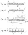
- FIG. 4Ais a schematic explanatory view for explaining each process in the flowchart in FIG. 3 , in which a semiconductor wafer has semiconductor devices formed thereon;
- FIG. 4Bis a schematic explanatory view for explaining each process in the flowchart in FIG. 3 , in which the semiconductor wafer has a protective sheet being applied in a protective sheet application process;
- FIG. 4Cis a schematic explanatory view for explaining each process in the flowchart in FIG. 3 , in which the semiconductor wafer is subjected to a polishing process;
- FIG. 4Dis a schematic explanatory view for explaining each process in the flowchart in FIG. 3 , in which the semiconductor wafer is subjected to a damaged layer removal process;
- FIG. 5Ais a schematic explanatory view for explaining each process in the flowchart in FIG. 3 , in which the semiconductor wafer has a mask layer formed in a mask layer formation process;
- FIG. 5Bis a schematic explanatory view for explaining each process in the flowchart in FIG. 3 , in which the semiconductor wafer has a dicing line mask removal portion and a bad mark mask removal portion formed in a mask layer partial removal process;
- FIG. 5Cis a schematic explanatory view for explaining each process in the flowchart in FIG. 3 , in which the semiconductor wafer is subjected to etching in a plasma dicing process;
- FIG. 5Dis a schematic explanatory view for explaining each process in the flowchart in FIG. 3 , in which the semiconductor wafer is diced into respective separate semiconductor devices;
- FIG. 5Eis a schematic explanatory view for explaining each process in the flowchart in FIG. 3 , in which the semiconductor wafer has the mask removed in a mask layer removal process;
- FIG. 5Fis a schematic explanatory view for explaining each process in the flowchart in FIG. 3 , in which the semiconductor wafer has a die bonding sheet applied thereto;
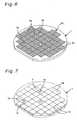
- FIG. 6is a schematic perspective view showing the semiconductor wafer having a mask pattern formed thereon;
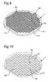
- FIG. 7is a schematic perspective view showing the semiconductor wafer having the mask removed after the plasma dicing
- FIG. 8Ais a schematic explanatory view for explaining part of the manufacturing process of semiconductor devices according to a second embodiment of the present invention, in which the semiconductor wafer has a mask layer formed in the mask layer formation process;
- FIG. 8Bis a schematic explanatory view for explaining part of the manufacturing process of semiconductor devices according to the second embodiment of the present invention, in which the semiconductor wafer has the mask layer partially removed in the mask layer partial removal process;
- FIG. 8Cis a schematic explanatory view for explaining part of the manufacturing process of semiconductor devices according to the second embodiment of the present invention, in which the semiconductor wafer is subjected to etching in the plasma dicing process;
- FIG. 8Dis a schematic explanatory view for explaining part of the manufacturing process of semiconductor devices according to the second embodiment of the present invention, in which the semiconductor wafer is diced into respective separate semiconductor devices;
- FIG. 8Eis a schematic explanatory view for explaining part of the manufacturing process of semiconductor devices according to the second embodiment of the present invention, in which a semiconductor wafer has the mask removed in the mask layer removal process;
- FIG. 8Fis a schematic explanatory view for explaining part of the manufacturing process of semiconductor devices according to the second embodiment of the present invention, in which the semiconductor wafer has a die bonding sheet applied thereto;
- FIG. 9is a schematic perspective view for showing the semiconductor wafer having mask patterns formed thereon in the second embodiment.
- FIG. 10is a schematic perspective view for showing the semiconductor wafer having the mask removed after the plasma dicing in the second embodiment.
- FIG. 1shows a schematic diagram schematically showing the structure of a plasma processing apparatus 101 exemplifying the semiconductor wafer dicing apparatus for implementing the semiconductor wafer dicing method in the first embodiment.
- the plasma processing apparatus 101applies plasma etching to a semiconductor wafer having a plurality of semiconductor devices formed thereon to conduct dicing (plasma dicing) of the semiconductor wafer into respective separate semiconductor devices.
- plasma dicingplasma dicing
- the plasma processing apparatus 101has a vacuum chamber 11 that includes a processing chamber 12 of an enclosed space for applying plasma processing to a semiconductor wafer 1 .
- a lower electrode 13 and an upper electrode 14are parallely disposed facing each other.
- a mounting face 13 a on which an almost disc-shaped semiconductor wafer 1 can be mountedis formed, and the semiconductor wafer 1 is mounted on the mounting face 13 a in the state that the entire periphery thereof is surrounded by an insulating ring 18 .
- the mounting face 13 ahas a function to suck and hold the mounted semiconductor wafer 1 in a releasably way through vacuum suction or electrostatic suction.
- the lower electrode 13is disposed inside the processing chamber 12 through an insulator 12 a , with the lower electrode 13 and the processing chamber 12 being electrically insulated through the insulator 12 a.
- a gas supply hole 14 awhich is a passage to supply plasma generation gas to the inside of a space (electric discharge space) formed between the upper electrode 14 and the lower electrode 13 , is formed in such a way as to go through the inside of the upper electrode 14 .
- one end of the gas supply hole 14 a in the upper electrode 14 formed to be linked to the outside of the vacuum chamber 11is connected to a plasma generation gas supply unit 17 provided outside of the vacuum chamber 11 , which makes it possible to supply, for example, a fluorinated plasma generation gas from the plasma generation gas supply unit 17 to the processing chamber 12 through the gas supply hole 14 a .
- a flow regulating valve 16exemplifying a gas flow rate regulating portion for regulating a supply gas flow rate to a desired flow rate is provided.
- a porous plate 15is seated on the lower surface of the upper electrode 14 as viewed in the drawing, which makes it possible to supply the plasma generation gas supplied through the gas supply hole 14 a to the inside of the processing chamber 12 in such a way as to be evenly sprayed to the semiconductor wafer 1 mounted on the mounting face 13 a of the lower electrode 13 through the porous plate 15 .
- the plasma processing apparatus 101has an air discharging pump 19 exemplifying an evacuation apparatus for reducing the pressure in the processing chamber 12 to a desired pressure (i.e., vacuumizing the processing chamber 12 ) by evacuating the processing chamber 12 .
- an RF power supply unit 20is electrically connected to the lower electrode 13 , which makes it possible to apply high-frequency voltage to the lower electrode 13 from the RF power supply unit 20 .
- the processing chamber 12is evacuated and vacuumized by the air discharging pump 19 and a high-frequency voltage is applied to the lower electrode 13 by driving the RF power supply unit 20 while a specified amount of the plasma generation gas is supplied to the processing chamber 12 from the plasma generation gas supply unit 17 , by which fluorinated plasma is generated between the electric discharge space between the upper electrode 14 and the lower electrode 13 .
- etchingi.e., plasma etching
- the plasma processing apparatus 101has a cooling unit 21 for cooling the semiconductor wafer 1 mounted on the mounting face 13 a of the lower electrode 13 through the mounting face 13 a by circulating a coolant inside the lower electrode 13
- the presence of the cooling unit 21makes it possible to prevent the temperature of the semiconductor wafer 1 from increasing beyond a specified temperature from the heat generated during plasma processing.
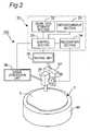
- a laser processing apparatus 102exemplifying the formation apparatus for semiconductor wafer dicing masks, in which during plasma dicing by such a plasma processing apparatus 101 , a mask layer placed on the surface of a semiconductor wafer 1 is processed with a laser beam along the dicing positions of respective semiconductor devices to form dicing lines, with reference to the schematic block diagram in FIG. 2 .
- the laser processing apparatus 102has a wafer holding unit 40 (wafer holding device) for holding the semiconductor wafer 1 having a mask layer 5 formed thereon in the state of being exposed in a releasably way.
- a moving plate moving head 37 equipped with a laser irradiation unit 39 and a camera 38is provided on the wafer holding unit 40 is, and further a moving apparatus (device) 35 for moving the moving plate moving head 37 relatively to the wafer holding unit 40 is provided along the surface of the semiconductor wafer 1 in the state of being held by the wafer holding unit 40 .
- the moving apparatus 35 moving the moving plate moving head 37allows the laser irradiation unit 39 and the camera 38 attached to the moving plate moving head 37 to be moved relatively to the wafer holding unit 40 .
- the laser irradiation unit 39is capable of irradiating the laser beam generated by a laser generation unit 36 to the semiconductor wafer 1 disposed below.
- the laser irradiation apparatus(device) comprises the laser irradiation unit 39 and the laser generation unit 36 .
- the camera 38is an infrared camera for picking images of the semiconductor wafer 1 disposed below by infrared light. In this case, images of a circuit pattern or distinguishing marks on the circuit formation face of the semiconductor wafer 1 may be picked up through the mask layer 5 . Then, the image pick-up result is inputted into a recognition section 34 included in a laser processing control unit 30 exemplifying a control device, where recognition processing is performed to detect the position and the circuit pattern arrangement of the semiconductor wafer 1 .
- the laser processing control unit 30comprises a control section 33 for controlling laser generation operation by the laser generation unit 36 , moving operation by the moving apparatus 35 and recognition processing by the recognition section 34 , an operation/input section 31 for operating and commanding the control by the control section 33 , and a work data storage section 32 for storing data which is referred during control operation by the control section 33 .
- the work data storage section 32stores data on dicing positions (dicing lines or parting lines) of respective semiconductor devices on the semiconductor wafer 1 and data on the width of the dicing lines formed at the dicing positions (dicing width), i.e., the removal width of the mask layer removed along the dicing positions. Data write onto the work data storage section 32 is executable by the operation/input section 31 .
- the control section 33controls the moving apparatus 35 based on an actual position data of the semiconductor wafer 1 detected by the recognition section 34 and the data on the dicing positions stored in the work data storage section 32 . With this, the moving apparatus 35 makes it possible to move the laser irradiation unit 39 along the dicing positions on the upper face of the semiconductor wafer 1 . Further, by the control section 33 controlling the laser generation unit 36 based on the data on the width of the dicing lines, it becomes possible to irradiate a laser beam with an output appropriate for removing the mask layer 5 with a removal width corresponding to the width of the dicing lines from the laser irradiation unit 39 . By executing such laser processing, it becomes possible to form a mask pattern with only a portion corresponding to the dicing lines for separating the semiconductor devices from each other being removed in the mask layer 5 on the surface of the semiconductor wafer 1 .
- FIG. 3shows a flowchart showing the procedures in the manufacturing process of the semiconductor devices
- FIGS. 4A, 4B , 4 C, 4 D, 5 A, 5 B, 5 C, 5 D, 5 E and 5 Fshow schematic explanatory views for explaining the procedures of the manufacturing process.
- step S 1 in the flowchart of FIG. 3the processing such as film formation, exposure and etching is applied to a circuit-formation-face 1 a that is a first surface of the semiconductor wafer 1 to form a plurality of circuit formation portions 2 which become semiconductor devices as shown in FIG. 4A (semiconductor device formation process). Further, in each of the circuit formation portions 2 , a plurality of external connection electrodes 3 are formed from conductive materials in the state of being exposed from the circuit-formation-face 1 a.
- the formation states of the respective circuit formation portions 2 and the external connection electrodes 3are inspected (semiconductor device inspection process, step S 2 ).
- semiconductor device inspection processstep S 2
- the quality checkis performed by every circuit formation portion 2 , and with respect to those circuit formation portions 2 determined to be flawed, their position information for the semiconductor wafer 1 is formed and stored.
- Such position informationmay be stored in a storage device included in the inspection apparatus for performing the inspection or may be stored in a storage device included in a management system for managing the entire manufacturing process of semiconductor devices and the like.
- the type of the storage configurationmay take various forms as long as the position information is stored in the state accessible in the following processes. Further, the position information is created and maintained not only in the case of the position information for those circuit formation portions 2 determined to be flawed, but in the case of the position information for the circuit formation portions 2 determined, on the contrary, to be acceptable, so that the acceptable circuit formation portions 2 may be distinguished from the flawed circuit formation portions 2 .
- a protective sheet 4is applied to the circuit-formation-face 1 a through an adhesive agent so as to prevent the circuit-formation-face 1 a of the semiconductor wafer 1 after completion of the inspection process from being damaged during each processing thereafter (protective sheet application process, step S 3 ).
- the protective sheet 4 for useis formed into almost the same shape as the external shape of the semiconductor wafer 1 so as to cover the entire circuit-formation-face 1 a and not to protrude outward from the end portion of the semiconductor wafer 1 .
- step S 41 in FIG. 3a polishing process for thinning the thickness of the semiconductor wafer 1 is performed. More specifically, as shown in FIG. 4C , with the circuit-formation-face 1 a of the semiconductor wafer 1 being on the lower side as viewed in the drawing, the semiconductor wafer 1 is placed on a holding table 42 through the protective sheet 4 and the placing position is held. In this state, a processing-target-face 1 b (second surface or mask placement-side surface on which a mask is placed in the following processes) that is a surface on the opposite side of the circuit-formation-face 1 a of the semiconductor wafer 1 is polished by using a grinding wheel 41 .
- a processing-target-face 1 bsecond surface or mask placement-side surface on which a mask is placed in the following processes
- the semiconductor wafer 1is thinned to have a thickness of about 100 ⁇ m or smaller, e.g., 50 ⁇ m in the first embodiment.
- a damaged layer retaining stress imparted by polishing with the grinding wheel 41is formed.
- Such a damaged layer being left on the formed semiconductor devicesdegrades the resistance of the semiconductor devices, and causes deterioration of their quality.
- the damaged layer formed on the processing-target-face 1 b of the semiconductor wafer 1is removed as shown in FIG. 4D (damaged layer removal process, step S 42 ). For example, as shown in FIG.
- an etching solution (sulfuric acid, nitric acid, phosphoric acid, fluorinated acid, etc.) 51is brought into contact with the damaged layer formed on the processing-target-face 1 b of the semiconductor wafer 1 so as to remove the damaged layer by corroding the damaged layer by the chemical reaction (wet etching treatment)
- wet etching treatmentinstead of by using the wet etching treatment as the removal processing of the damaged layer, the damaged layer may be removed by applying plasma etching to the processing-target-face 1 b (plasma etching process), or the damaged layer may be removed by performing polishing on the processing-target-face 1 b .
- the process combining the polishing process in step S 41 and the damaged layer removal process in step S 42constitutes the thinning process in step S 4 .
- a mask layer 5is formed on the processing-target-face 1 b of the semiconductor wafer 1 (mask layer formation process, step S 51 ).
- the mask layer 5is for forming mask patterns for use in the later-described plasma dicing process, the mask pattern being formed from a material, such as aluminum and resin, having tolerance against plasma produced with use of fluorinated gasses.
- a method for forming an aluminum thin film on the processing-target-face 1 b by deposition and a method for applying a foil-like aluminum thin filmare used.
- resina method for applying a resin formed in a film shape and a method for coating the processing-target-face 1 b with a liquid resin by spin coat method and the like may be used.
- partial removal of the mask layer 5 by laser processingis performed (mask layer partial removal process, step S 52 ). More specifically, in the laser processing apparatus 102 shown in FIG. 2 , the semiconductor wafer 1 having the mask layer 5 formed on the processing-target-face 1 b is placed on the wafer holding unit 40 through the protective sheet 4 which is applied to the circuit-formation-face 1 a , and the placing position is held. After that, while the camera 38 is moved by the moving apparatus 35 along the surface of the semiconductor wafer 1 , an image of the circuit patterns of the semiconductor wafer 1 is obtained. By performing recognition processing of the obtained image in the recognition section 34 , the actual position of the semiconductor wafer 1 is recognized.
- the control section 33controls the moving apparatus 35 based on the result of the recognition processing and the position data on the dicing positions (positions of the dicing lines) stored in the work data storage section 32 , and moves the laser irradiation unit 39 along the dicing positions of the semiconductor wafer 1 . While moving the laser irradiation unit 39 , the control section 33 controls the laser generation unit 36 based on the data on the width of the dicing lines, and irradiates a laser beam with an output appropriate for removing the mask layer 5 with a removal width corresponding to the width. With such irradiation of the laser beam 39 a , a dicing mask removal portion 5 a where the mask layer 5 is partially removed is formed at the dicing positions of the respective semiconductor devices as shown in FIG. 5B .
- the position information of the flawed circuit formation portions 2 created based on the inspection result of the previously performed semiconductor device inspection process(step S 2 ), i.e., the position information for the flawed semiconductor devices, are inputted through the operation/input section 31 .
- Such input of the position informationmay be conducted through wireless communication means, wire communication means or storage media.
- the control section 33controls the moving apparatus 35 , the laser generation unit 36 and the laser irradiation unit 39 based on the position information for the flawed semiconductor devices held in the work data storage section 32 so as to irradiate the laser beam 39 a to the mask layer 5 placed on the processing-target-face 1 b of the flawed semiconductor devices, by which the mask layer 5 is partially removed so as to expose a part of the processing-target-face 1 b of the flawed semiconductor devices.
- the mask layer 5is partially removed so as to expose an almost central area of the processing-target-face 1 b of the flawed semiconductor device in an almost circular shape.
- a portion of the mask layer 5 partially removed by such wayis a bad mark mask removal portion 5 b on which a bad mark (flawed semiconductor device distinguishing mark) is formed in the following plasma dicing process.
- the partial removal of the mask layer 5is executed so as to partially expose the surfaces of all the flawed semiconductor devices.
- the partial removal of the mask layer 5is not executed. Portions of the mask layer 5 remaining after portions corresponding to the dicing mask removal portion 5 a and the bad mark mask removal portion 5 b are removed make masks 5 C, and portions (surfaces) of the masks 5 C are portions to which etching is not applied during the later-executed plasma dicing.
- the inspection of the semiconductor devicesis performed from the side of the circuit-formation-face 1 a , whereas in the laser processing apparatus 102 , the mask layer 5 disposed on the side of the processing-target-face 1 b of the semiconductor wafer 1 is processed. Therefore, the position information for the flawed semiconductor devices created and obtained during the inspection process is handled as information in which the upper and lower faces of the semiconductor wafer 1 being inverted in the laser processing. Moreover, the position information of such flawed semiconductor devices and dicing line data may be combined to constitute mask data for formation of mask patterns.
- mask patterns 5 bas shown in the schematic perspective view of the semiconductor wafer 1 in FIG. 6 are formed.
- Such mask patterns 5 bcomprises the dicing line mask removal portions 5 a , the bad mark mask removal portions 5 b and the masks 5 c , and in the case of the semiconductor wafer 1 shown in FIG. 6 , three flawed semiconductor devices are present.
- description is given of the case where in the outer peripheral portion of the semiconductor wafer 1 , the mask layer 5 on a portion without the semiconductor devices is also removed in FIG. 6the present embodiment is not limited to this case and therefore is applicable to the case where, for example, the mask layer 5 on this portion is not removed.
- the semiconductor wafer 1is placed on the placing face 13 a of the lower electrode 13 through the protective sheet 4 with the processing-target-face 1 b having the mask patterns 5 d formed thereon being the upper face.
- the vacuum chamber 11is enclosed and the air discharging pump 19 is driven to vacuumize the processing chamber 12 (e.g., to approx 100 Pa), while a gas is supplied at a flow rate regulated by the flow regulating valve 16 from the plasma generation gas supply unit 17 to the inside of the processing chamber 12 through the gas supply hole 14 a and the porous plate 15 .
- a high-frequency voltageis applied to the lower electrode 13 from the RF power supply unit 20 so that plasma is generated in the electric discharge space between the upper electrode 14 and the lower electrode 13 .
- a plasma 61 generated in the electric discharge spaceis irradiated to the mask patterns 5 d formed on the processing-target-face 1 b of the semiconductor wafer 1 in the state of being placed on the placing face 13 a of the lower electrode 13 .
- the surfaces of the processing-target-face 1 b corresponding to the dicing mask removal portions 5 a and the bad mark mask removal portions 5 bwhich are the exposed surfaces without the mask 5 C formed thereon, are irradiated with the plasma 61 .
- the exposed surfaces of the processing-target-face 1 bare subjected to etching.
- the semiconductor wafer 1is diced into respective separate semiconductor devices 1 d along dicing lines 1 c , and almost circular-shaped through hole are formed as bad marks 1 e in a central area of flawed semiconductor devices 1 f along the bad mark mask removal portions 5 b.
- FIG. 7shows a schematic perspective view of the semiconductor wafer 1 subjected to the mask layer removal process.
- the respective semiconductor devices 1 d and the flawed semiconductor devices 1 fare separated into respective pieces, and in the central area of the each of the flawed semiconductor devices 1 f , the bad mark 1 e is formed as an almost circular-shaped through hole.
- an adhesive sheet (die bonding sheet) 6is applied to the processing-target-face 1 b of the semiconductor wafer 1 (die bonding sheet application process, step S 8 ), and the protective sheet 4 protecting the circuit-formation-face 1 a of the semiconductor wafer 1 is removed.
- the adhesive sheet 6herein has a size larger than the semiconductor wafer 1 and is fixed to its surrounding by an unshown wafer-ring (jig). Holding the wafer-ring allows handling of the semiconductor wafer 1 . With this, the manufacturing process of semiconductor devices is completed.
- each circuit-formation-face 1 a of the semiconductor devices 1 d in the state of adhering to the adhesive sheet 6is sucked and held by, for example, a suction nozzle, and in this state, the suction nozzle is raised so that the sucked and held semiconductor devices 1 d can be removed from the adhesive sheet 6 and be picked up.
- an image of the circuit-formation-face 1 a of the semiconductor devices 1 dis obtained by an image pickup apparatus and the image is subjected to recognition processing, by which those semiconductor devices 1 d to be picked up are identified. As shown in FIG.
- the flawed semiconductor device 1 fsince the flawed semiconductor device 1 f has the circular-shaped through hole formed as the bad mark 1 e , light reflectance on its circuit-formation-face 1 a is largely difference from the circuit-formation-face 1 a of the other semiconductor devices 1 d , which makes it possible to clearly distinguish the flawed semiconductor device 1 f from the other semiconductor devices 1 d during the above-stated recognition processing. Therefore, it becomes possible to securely prevent the flawed semiconductor device 1 f from being picked up by mistake during picking-up of the semiconductor devices 1 d.
- suction and holding of the semiconductor devices 1 d by the suction nozzleis implemented by sucking and holding the almost central area of the circuit-formation-face 1 a , and since the flawed semiconductor device 1 f has the almost circular-shaped through hole formed as the bad mark 1 e , suction and holding of the circuit-formation-face 1 a of the flawed semiconductor device can also be structurally prevented.
- the bad mark 1 e formed on such flawed semiconductor devices 1 fallows an operator to clearly recognize by sight, thereby making it possible to clearly distinguish the flawed semiconductor device 1 f from the other semiconductor devices 1 d.
- the size of the bad mark 1 e formed on such flawed semiconductor devices 1 fis determined by depending on the size (planar size) of semiconductor devices (or flawed semiconductor devices), and is preferably determined, for example, in the size range of about 10% to 40% of the size is of the semiconductor device.
- the size of the bad mark 1 eis preferably not less than the size which enables the visible recognition apparatus to surely recognize whether or not the bad mark 1 e is formed on a certain semiconductor device 1 d , when the semiconductor 20 device 1 d is sucked and held from the semiconductor wafer 1 which was diced and is covered with the adhesive sheet 6 in a die bonding apparatus or the like.
- the bad mark 1 eis not limited to those formed as the through holes as describe above.
- the bad markmay be formed by removing a part thereof, e.g., about a half depth thereof.
- the formed bad markneeds to have a recognizable size. Therefore, in the present specification, “removal” of the exposed portion in the bad mark mask removal portion herein signifies not only the case of “complete” removal but also the case of “partial” removal.
- the formation of the bad marks 1 e for clearly distinguishing such flawed semiconductor devices 1 f from the other semiconductor devices 1 dis achieved by performing plasma dicing with use of the bad mark mask removal portions 5 b formed together with the dicing mask removal portions 5 a which defines the dicing lined in the mask pattern formation process. Therefore, an additional new process for formation of such bad marks 1 e is not necessary, and therefore forming of the bad marks 1 e make efficient.
- the bad mark 1 eis not formed as the prominent portion with use of inks and resist layers like conventional bad marks but formed as the almost-circular-shaped through hole, and further, since the formation of the bad mark 1 e is performed after the thinning processing of the semiconductor wafer 1 is executed, recess portions and the like formed on the surface of the semiconductor wafer 1 due to the thinning processing can be surely prevented, thereby allowing manufacturing of high-quality semiconductor devices.
- the size and the prominence height of the respective external connection electrodes 3 formed on the circuit-formation-face 1 a of the respective semiconductor devicesare sufficiently smaller (e.g., about 1 ⁇ 5 to 1/10 times) than the size and the prominence height of the prominent portion of the conventional bad mark formed with use of inks and the resist layers, the extrusions or indentions of the circuit-formation-face 1 a caused by formation of these external connection electrodes 3 can be sufficiently absorbed by the protective sheet 4 applied to the circuit-formation-face 1 a , and will not exert an influence during the thinning processing.
- the dicing mask removal portions 5 acan be formed between the flawed semiconductor device 1 f and the adjacent semiconductor devices 1 d .
- the etching statecan be maintained almost uniform. Therefore, plasma dicing can be conducted under the uniform conditions despite whether adjacent semiconductor devices are the flawed semiconductor devices or not, which makes it possible to manufacture high-quality semiconductor devices.
- FIGS. 8A, 8B , 8 C, 8 D, 8 E, and 8 Fshow the schematic explanatory views for showing part of the procedures in the manufacturing method for semiconductor devices according to a second embodiment of the present invention.
- the manufacturing method for semiconductor devices in the second embodimentwhich is performed in the procedures similar to those in the flowchart in FIG. 3 showing the procedures in the manufacturing method in the first embodiment, is different from the first embodiment in the point that the formation of the bad mark is not involved and the flawed semiconductor device itself is removed by etching during plasma etching.
- descriptionis given on the different point.
- a mask layer 5is formed on a processing-target-face 1 b of the semiconductor wafer 1 after thinning processing is applied and removal the damaged layer is performed.
- the formed mask layer 5is processed with the laser beam 39 a to form the dicing mask removal portion 5 a along dicing positions (positions of the dicing lines).
- processing with the laser beam 39 ais performed so as to totally remove the mask layer 5 placed on the processing-target-face 1 b of the flawed semiconductor devices. More specifically, as shown in FIG.
- FIG. 9shows a schematic perspective view of the semiconductor wafer 1 with the mask patterns 5 d formed thereon by such partial removal of the mask layer 5 .
- portions denoted by reference numeral P 1correspond to the flawed semiconductor devices with the mask layer 5 removed, and on this semiconductor wafer 1 , three flawed semiconductor devices are present.
- FIG. 8Cplasma etching is applied to the semiconductor wafer 1 having the mask pattern 5 d formed thereon in the plasma processing apparatus 101 .
- the processing-target-face 1 b with the dicing mask removal portion 5 a formed thereon and the processing-target-face 1 b of the flawed semiconductor devicesare irradiated with the plasma 61 and are subjected to etching.
- FIG. 8Dthe semiconductor wafer 1 is diced into respective separate semiconductor devices 1 d and the flawed semiconductor devices themselves are removed and eliminated.
- the mask removal processis performed as shown in FIG. 8F
- the die bonding sheet application processis performed as shown in FIG. 8 , by which the manufacturing process of semiconductor devices is completed.
- FIG. 10shows a schematic perspective view of the semiconductor wafer 1 on which the flawed semiconductor devices are removed and which is diced into respective separate semiconductor devices 1 d as viewed from the side of the processing-target-face 1 b .
- FIG. 10indicates that semiconductor devices 1 d are removed (eliminated) at three locations as denoted by reference numeral P 2 on the semiconductor wafer 1 .
- the flawed semiconductor devicesare completely removed and eliminated, and therefore as shown in FIG. 8F , the respective semiconductor devices 1 d in the final manufacturing stage do not include the flawed semiconductor devices themselves. Therefore, during picking-up of the semiconductor devices 1 d performed thereafter, picking-up of the flawed semiconductor devices by mistake can be prevented completely.
- the mask constituting the mask patterns created in advance based on the position information of the flawed semiconductor devicesmay be placed on the processing-target-face 1 b of the semiconductor wafer 1 so as to partially or completely expose the surface of the flawed semiconductor devices.
- the mask data created in combination of the position information of the flawed semiconductor devices and dicing line informationmay be inputted into the laser processing apparatus 102 for processing the mask layer 5 based on the mask data.
- the bad marksmay be formed on the flawed semiconductor devices, or the flawed semiconductor devices themselves may be eliminated, and the method therefore may take various forms.
- the bad mark mask removal portion 5 bis not limited to those formed as almost circular-shaped through holes as shown in the first embodiment, but may include those formed as, for example, polygon-shaped or oval-shaped through holes. Further, a plurality of the bad mark mask removal portions 5 b may be formed for one flawed semiconductor device 1 f . Further, in the case where a flawed semiconductor device 1 f is disposed on the outermost portion of the semiconductor wafer 1 in FIG. 6 , instead of forming the bad mark mask removal portion in an almost central area of the flawed semiconductor device 1 f , the bad mark mask removal portion may be formed so as to exclude the peripheral end side where the semiconductor devices 1 d are not disposed adjacently. In such a case, the bad mark mask removal portion 5 b may still be formed between the adjacent semiconductor devices 1 d to maintain the uniformity of etching.
Landscapes
- Engineering & Computer Science (AREA)
- Physics & Mathematics (AREA)
- Condensed Matter Physics & Semiconductors (AREA)
- General Physics & Mathematics (AREA)
- Computer Hardware Design (AREA)
- Microelectronics & Electronic Packaging (AREA)
- Power Engineering (AREA)
- Manufacturing & Machinery (AREA)
- Dicing (AREA)
Abstract
Description
- The present invention relates to a dicing method for a semiconductor wafer in which a semiconductor wafer with a plurality semiconductor devices formed thereon is diced into the respective separate semiconductor devices by application of plasma etching, a manufacturing method for semiconductor devices including such a dicing method involving the plasma etching as a part of its process, and a formation apparatus for semiconductor wafer dicing masks for forming semiconductor wafer dicing masks for defining dicing lines used for dicing of the respective separate semiconductor devices through the plasma etching.
- Conventionally, in manufacturing of such semiconductor devices, after a plurality of semiconductor devices are formed on a circuit formation face of a semiconductor wafer, the formed semiconductor devices undergo an inspection (mainly an inspection of electric characteristic), and based on the result of quality check, flawed (bad) semiconductor devices are marked, for example, on their surfaces, so as to be visibly distinguishable from other semiconductor devices for management of the flawed semiconductor devices.
- As such conventional marking methods, a method for forming bad marks on the surface of the flawed semiconductor devices with inks and a method for forming bad marks through formation of resist films are known (see, e.g., Japanese unexamined patent publication No. 2000-124270 A).
- After the inspection of the semiconductor devices, and formation of bad marks on the flawed semiconductor devices reflecting the result of the inspection, polishing process is performed on the face of the opposite side for the circuit formation face of the semiconductor wafer as a thinning processing of the semiconductor wafer to the level of, for example, a thickness of 100 μm or smaller.
- However, by forming such bad marks (formed on the circuit formation face), smooth protuberant portions (protuberance layer) are formed only on portions of the circuit formation face of the semiconductor wafer where the bad marks are formed. Thus, with the protuberant portions partially formed on the circuit formation face, as a result of polishing process performed on the opposite face, smooth recess portions are formed in turn on portions corresponding to the places where the protuberant portions are formed on the pertinent face. This causes such problem as degraded quality of semiconductor devices as the formation of the bad marks aiming at quality management of the semiconductor devices contrarily hinders the uniformity of the thickness of manufactured semiconductor devices. Particularly, the thinned semiconductor wafer is often required a higher-level uniformity of the thickness, making occurrence of such a problem more prominent.
- An object of the present invention is to provide, for solving the problem, a dicing method for semiconductor wafer capable of distinguishing flawed semiconductor devices from other semiconductor devices while preventing degradation of the quality of the respective semiconductor devices in a semiconductor wafer, a manufacturing method for semiconductor devices, and a formation apparatus for semiconductor wafer dicing masks for use during dicing of the semiconductor devices.
- In order to accomplish the object, the present invention is constituted as shown below.
- According to a first aspect of the present invention, there is provided a manufacturing method for semiconductor devices comprising:
- placing a mask on a mask placement-side surface of a semiconductor wafer in which a plurality of semiconductor devices are formed, while defining dicing lines for dicing the semiconductor wafer into the respective separate semiconductor devices and partially exposing the mask placement-side surface on a flawed semiconductor device among the respective semiconductor devices; and
- dicing (separating or dividing) the semiconductor wafer into the respective semiconductor devices along the defined dicing lines and removing an exposed portion of the flawed semiconductor device so as to form a removed portion as a distinguishing mark for the flawed semiconductor device, by applying plasma etching to the mask placement-side surface of the semiconductor wafer, thereby the separated respective semiconductor devices distinguishably from the flawed semiconductor devices are manufactured.
- According to a second aspect of the present invention, there is provided the manufacturing method for semiconductor devices as defined in the first aspect, wherein the mask is placed so as to partially expose the surface of the flawed semiconductor device on basis of position information for the flawed semiconductor device in the semiconductor wafer.
- According to a third aspect of the present invention, there is provided the manufacturing method for semiconductor devices as defined in the first aspect, further comprising:
- obtaining position information for the flawed semiconductor device in the semiconductor wafer before placing the mask, wherein
- the mask is placed on basis of the obtained position information for the flawed semiconductor device.
- According to a fourth aspect of the present invention, there is provided the manufacturing method for semiconductor devices as defined in second aspect, wherein the position information for the flawed semiconductor device is formed by using a result of an inspection performed on the respective semiconductor devices in the semiconductor wafer.
- According to a fifth aspect of the present invention, there is provided the manufacturing method for semiconductor devices as defined in the first aspect, wherein in placing of the mask,
- the mask is placed so as to cover the entire mask placement-side surface of the semiconductor wafer, and then
- parts of the mask are removed in conformity with the respective positions of the dicing lines on the semiconductor wafer so as to partially expose the surface of the semiconductor wafer to define the dicing lines, and a part of the mask on the flawed semiconductor device is removed so as to partially expose the surface of the flawed semiconductor device.
- According to a sixth aspect of the present invention, there is provided the manufacturing method for semiconductor devices as defined in the fifth aspect, wherein the mask is removed by irradiating a laser beam to the mask of the semiconductor wafer while moving the laser beam relatively along to the surface of the semiconductor wafer.
- According to a seventh aspect of the present invention, there is provided the manufacturing method for semiconductor devices as defined in the sixth aspect, wherein the laser beam is relatively moved on basis of preset mask data.
- According to an eighth aspect of the present invention, there is provided the manufacturing method for semiconductor devices as defined in the sixth aspect, wherein the laser beam is relatively moved, on basis of position information for the dicing lines and position information for the flawed semiconductor device in the semiconductor wafer.
- According to a ninth aspect of the present invention, there is provided the manufacturing method for semiconductor devices as defined in the first aspect, wherein the mask is placed so as to expose an almost central area of the surface of the flawed semiconductor device in an almost circular shape.
- According to a tenth aspect of the present invention, there is provided the manufacturing method for semiconductor devices as defined in the first aspect, further comprising:
- removing the respective masks from the mask placement-side surface of the semiconductor wafer, after dicing the semiconductor and removing the exposed portion.
- According to an eleventh aspect of the present invention, there is provided the manufacturing method for semiconductor devices as defined in the fourth aspect, wherein
- after the inspection of the respective semiconductor devices, thinning of the semiconductor wafer is performed, and then
- the mask is placed on the thinned semiconductor wafer.
- According to a twelfth aspect of the present invention, there is provided a manufacturing method for semiconductor devices comprising:
- placing a mask on a mask placement-side surface of a semiconductor wafer in which a plurality of semiconductor devices are formed, while defining dicing lines for dicing the semiconductor wafer into the respective separate semiconductor devices and entirely exposing the mask placement-side surface on a flawed semiconductor device among the respective semiconductor devices; and
- dicing the semiconductor wafer into the respective semiconductor devices along the defined dicing lines and removing the flawed semiconductor device entirely, by applying plasma etching to the mask placement-side surface of the semiconductor wafer, thereby the separated respective semiconductor devices are manufactured.
- According to a thirteenth aspect of the present invention, there is provided the manufacturing method for semiconductor devices as defined in the twelfth aspect, wherein the mask is placed so as to entirely expose the surface of the flawed semiconductor device on basis of position information for the flawed semiconductor device in the semiconductor wafer.
- According to a fourth aspect of the present invention, there is provided the manufacturing method for semiconductor devices as defined in the twelfth aspect, further comprising:
- obtaining position information for the flawed semiconductor device in the semiconductor wafer before placing of the mask, wherein
- the mask is placed on basis of the obtained position information for the flawed semiconductor device.
- According to a fifth aspect of the present invention, there is provided the manufacturing method for semiconductor devices as defined in the thirteenth aspect, wherein the position information for the flawed semiconductor device is formed by using a result of an inspection performed on the respective semiconductor devices in the semiconductor wafer.
- According to a sixteenth aspect of the present invention, there is provided the manufacturing method for semiconductor devices as defined in the twelfth aspect, wherein in placing of the mask,
- the mask is placed so as to cover the entire mask placement-side surface of the semiconductor wafer, and then
- parts of the mask are removed in conformity with the respective positions of the dicing lines on the semiconductor wafer so as to partially expose the surface of the semiconductor wafer to define the dicing lines, and the entire mask on the flawed semiconductor device is removed so as to entirely expose the surface of the flawed semiconductor device.
- According to a seventeenth aspect of the present invention, there is provided the manufacturing method for semiconductor devices as defined in the sixteenth aspect, wherein the mask is removed by irradiating a laser beam to the mask of the semiconductor wafer while moving the laser beam relatively along to the surface of the semiconductor wafer.
- According to an eighteenth aspect of the present invention, there is provided the manufacturing method for semiconductor devices as defined in the seventeenth aspect, wherein the laser beam is relatively moved on basis of preset mask data.
- According to a nineteenth aspect of the present invention, there is provided the manufacturing method for semiconductor devices as defined in the seventeenth aspect, wherein the laser beam is relatively moved on basis of position information for the dicing lines and position information for the flawed semiconductor device in the semiconductor wafer.
- According to a twentieth aspect of the present invention, there is provided the manufacturing method for semiconductor devices as defined in the twelfth aspect, further comprising:
- removing the respective masks from the mask placement-side surface of the semiconductor wafer, after dicing the semiconductor wafer and removing the exposed portion.
- According to a 21st aspect of the present invention, there is provided the manufacturing method for semiconductor devices as defined in the fifteenth aspect, wherein
- after the inspection of the respective semiconductor devices, thinning of the semiconductor wafer is performed, and then
- the mask is placed on the thinned semiconductor wafer.
- According to a 22nd aspect of the present invention, there is provided a formation apparatus for semiconductor wafer dicing masks for defining dicing lines to dice a semiconductor wafer, in which a plurality of semiconductor devices are formed, into respective separate semiconductor devices through plasma etching processing by partial removal of a mask placed so as to cover an entire mask placement-side surface of the semiconductor wafer, comprising:
- a wafer holding device for holding the semiconductor wafer;
- a laser irradiation device for irradiating a laser beam to the mask on the semiconductor wafer held by the wafer holding device so as to remove an irradiated portion of the mask;
- a moving device for relatively moving the wafer holding device and the laser irradiation device in directions along the surface of the semiconductor wafer; and
- a control device having position information for the dicing lines and position information for a flawed semiconductor device among the respective semiconductor is devices, which is operable to remove a portion of the mask corresponding to the dicing lines and remove the mask so as to partially or entirely expose the surface of the flawed semiconductor device, by controlling operations of the laser irradiation device and the moving device on basis of the position information for the dicing lines, and thereby the semiconductor wafer dicing mask is formed.
- According to the first aspect of the present invention, when a mask for defining dicing lines of the respective semiconductor devices is placed on the mask placement-side surface of the semiconductor wafer, the placement is performed so as to partially expose the surface of a flawed semiconductor device, and then plasma etching is applied, so that the semiconductor wafer is diced into the respective separate semiconductor devices along the dicing lines and at the same time (simultaneously) an exposed portion of the flawed semiconductor device is removed so as to form the removed portion into a flawed semiconductor device distinguishing mark (bad mark). Thus, by forming the flawed semiconductor device distinguishing mark through plasma etching in the final stage of the manufacturing process of the semiconductor devices, it becomes possible to prevent occurrence of such conventional problem that bad marks with use of inks and resist films which are formed as prominent portions cause dispersion of the thickness of the semiconductor wafer through the thinning processing.
- Moreover, the plasma etching for dicing the semiconductor device into the respective separate semiconductor devices allows the dicing together with the formation of the bad marks, which makes it possible to provide a dicing method for semiconductor wafers capable of realizing efficient formation of the bad marks, i.e., a manufacturing method for semiconductor devices.
- Therefore, it becomes possible to efficiently form the distinguishing marks allowing clear distinction of the flawed semiconductor device from other semiconductor devices without degrading the quality of the semiconductor devices, and to stabilize the quality of the diced semiconductor devices.
- According to the second aspect or the third aspect of the present invention, by conducting such placement of the mask based on the position information for the flawed semiconductor device, it becomes possible to specifically realize the formation of the bad marks and the dicing with use of, for example, automated apparatuses and the like.
- According to the fourth aspect of the present invention, since the position information for such a flawed semiconductor device is position information formed based on the result of the inspection performed on the respective semiconductor devices, the information obtained from the inspection process can be directly linked to the formation of the bad marks on the flawed semiconductor devices, thereby allowing reliable formation of the bad marks.
- According to the fifth aspect of the present invention, the formation of the mask is achieved by placing the mask in such a way as to cover the entire mask placement-side surface of the semiconductor wafer and by applying processing to partially remove the placed mask.
- According to the sixth aspect, the seventh aspect or the eighth aspect of the present invention, the processing of the mask can be specifically realized with use of laser beams. Moreover, by relatively moving the laser beam and the semiconductor wafer during such processing based on mask data and position information for the flawed semiconductor device, the mask at a desired position will be credibly removed
- According to the ninth aspect of the present invention, by placing the mask so as to expose an almost central area of the surface of the flawed semiconductor device in an almost circular shape, the dicing lines defined by the mask are definitely positioned between the flawed semiconductor devices and the adjacent semiconductor devices, which makes it possible to maintain the uniformity of etching of dicing position portions in the plasma etching operation and to provide high-quality semiconductor devices.
- According to another aspect of the present invention, during the placement of the mask, instead of being partially exposed, the surface of the flawed semiconductor device is totally exposed, so that the flawed semiconductor device itself is removed by the plasma etching. Thus, removing the flawed semiconductor device itself makes it possible to credibly prevent the flawed semiconductor device from being confused with other semiconductor devices.
- Moreover, by incorporating such semiconductor wafer dicing methods of the respective aspects in the manufacturing process of semiconductor devices, it becomes possible to provide a manufacturing method for semiconductor devices capable of covering acquisition of the position information for flawed semiconductor devices from the inspection process to dicing of the semiconductor wafer into the respective separate semiconductor devices performed together with formation of the bad marks.
- These and other aspects and features of the present invention will become clear from the following description taken in conjunction with the preferred embodiments thereof with reference to the accompanying drawings, in which:
FIG. 1 is a schematic diagram for showing a plasma processing apparatus for use in the manufacturing process of semiconductor devices according to a first embodiment of the present invention;FIG. 2 is a schematic diagram for showing a laser processing apparatus for use in the manufacturing process of the semiconductor devices in the first embodiment of the present invention;FIG. 3 is a flowchart showing the procedures of the semiconductor device manufacturing process in the first embodiment;FIG. 4A is a schematic explanatory view for explaining each process in the flowchart inFIG. 3 , in which a semiconductor wafer has semiconductor devices formed thereon;FIG. 4B is a schematic explanatory view for explaining each process in the flowchart inFIG. 3 , in which the semiconductor wafer has a protective sheet being applied in a protective sheet application process;FIG. 4C is a schematic explanatory view for explaining each process in the flowchart inFIG. 3 , in which the semiconductor wafer is subjected to a polishing process;FIG. 4D is a schematic explanatory view for explaining each process in the flowchart inFIG. 3 , in which the semiconductor wafer is subjected to a damaged layer removal process;FIG. 5A is a schematic explanatory view for explaining each process in the flowchart inFIG. 3 , in which the semiconductor wafer has a mask layer formed in a mask layer formation process;FIG. 5B is a schematic explanatory view for explaining each process in the flowchart inFIG. 3 , in which the semiconductor wafer has a dicing line mask removal portion and a bad mark mask removal portion formed in a mask layer partial removal process;FIG. 5C is a schematic explanatory view for explaining each process in the flowchart inFIG. 3 , in which the semiconductor wafer is subjected to etching in a plasma dicing process;FIG. 5D is a schematic explanatory view for explaining each process in the flowchart inFIG. 3 , in which the semiconductor wafer is diced into respective separate semiconductor devices;FIG. 5E is a schematic explanatory view for explaining each process in the flowchart inFIG. 3 , in which the semiconductor wafer has the mask removed in a mask layer removal process;FIG. 5F is a schematic explanatory view for explaining each process in the flowchart inFIG. 3 , in which the semiconductor wafer has a die bonding sheet applied thereto;FIG. 6 is a schematic perspective view showing the semiconductor wafer having a mask pattern formed thereon;FIG. 7 is a schematic perspective view showing the semiconductor wafer having the mask removed after the plasma dicing;FIG. 8A is a schematic explanatory view for explaining part of the manufacturing process of semiconductor devices according to a second embodiment of the present invention, in which the semiconductor wafer has a mask layer formed in the mask layer formation process;FIG. 8B is a schematic explanatory view for explaining part of the manufacturing process of semiconductor devices according to the second embodiment of the present invention, in which the semiconductor wafer has the mask layer partially removed in the mask layer partial removal process;FIG. 8C is a schematic explanatory view for explaining part of the manufacturing process of semiconductor devices according to the second embodiment of the present invention, in which the semiconductor wafer is subjected to etching in the plasma dicing process;FIG. 8D is a schematic explanatory view for explaining part of the manufacturing process of semiconductor devices according to the second embodiment of the present invention, in which the semiconductor wafer is diced into respective separate semiconductor devices;FIG. 8E is a schematic explanatory view for explaining part of the manufacturing process of semiconductor devices according to the second embodiment of the present invention, in which a semiconductor wafer has the mask removed in the mask layer removal process;FIG. 8F is a schematic explanatory view for explaining part of the manufacturing process of semiconductor devices according to the second embodiment of the present invention, in which the semiconductor wafer has a die bonding sheet applied thereto;FIG. 9 is a schematic perspective view for showing the semiconductor wafer having mask patterns formed thereon in the second embodiment; andFIG. 10 is a schematic perspective view for showing the semiconductor wafer having the mask removed after the plasma dicing in the second embodiment.- Before the description of the present invention proceeds, it is to be noted that like parts are designated by like reference numerals throughout the accompanying drawings.
- Hereinbelow, the embodiment of the present invention will be described in detail with reference to the drawings.
- For describing a semiconductor wafer dicing method and a semiconductor device manufacturing method according to a first embodiment of the present invention, first, the structure of the apparatuses for use in the dicing method and the manufacturing method will be described.
FIG. 1 shows a schematic diagram schematically showing the structure of aplasma processing apparatus 101 exemplifying the semiconductor wafer dicing apparatus for implementing the semiconductor wafer dicing method in the first embodiment. Theplasma processing apparatus 101 applies plasma etching to a semiconductor wafer having a plurality of semiconductor devices formed thereon to conduct dicing (plasma dicing) of the semiconductor wafer into respective separate semiconductor devices. First, the outlined structure of theplasma processing apparatus 101 will be described hereinbelow with reference toFIG. 1 .- As shown in
FIG. 1 , theplasma processing apparatus 101 has avacuum chamber 11 that includes aprocessing chamber 12 of an enclosed space for applying plasma processing to asemiconductor wafer 1. Inside thevacuum chamber 11, alower electrode 13 and anupper electrode 14 are parallely disposed facing each other. Moreover, on the upper face of thelower electrode 13 as viewed in the drawing, a mountingface 13aon which an almost disc-shapedsemiconductor wafer 1 can be mounted is formed, and thesemiconductor wafer 1 is mounted on the mountingface 13ain the state that the entire periphery thereof is surrounded by an insulatingring 18. Moreover, the mountingface 13ahas a function to suck and hold the mountedsemiconductor wafer 1 in a releasably way through vacuum suction or electrostatic suction. Thelower electrode 13 is disposed inside theprocessing chamber 12 through aninsulator 12a, with thelower electrode 13 and theprocessing chamber 12 being electrically insulated through theinsulator 12a. - Moreover, in the
upper electrode 14, agas supply hole 14a, which is a passage to supply plasma generation gas to the inside of a space (electric discharge space) formed between theupper electrode 14 and thelower electrode 13, is formed in such a way as to go through the inside of theupper electrode 14. Moreover, one end of thegas supply hole 14ain theupper electrode 14 formed to be linked to the outside of thevacuum chamber 11 is connected to a plasma generationgas supply unit 17 provided outside of thevacuum chamber 11, which makes it possible to supply, for example, a fluorinated plasma generation gas from the plasma generationgas supply unit 17 to theprocessing chamber 12 through thegas supply hole 14a. It is to be noted that at some midpoint of the gas supply passage extending between the plasma generationgas supply unit 17 and the one end of thegas supply hole 14a, aflow regulating valve 16 exemplifying a gas flow rate regulating portion for regulating a supply gas flow rate to a desired flow rate is provided. Further, aporous plate 15 is seated on the lower surface of theupper electrode 14 as viewed in the drawing, which makes it possible to supply the plasma generation gas supplied through thegas supply hole 14ato the inside of theprocessing chamber 12 in such a way as to be evenly sprayed to thesemiconductor wafer 1 mounted on the mountingface 13aof thelower electrode 13 through theporous plate 15. - Moreover, the
plasma processing apparatus 101 has anair discharging pump 19 exemplifying an evacuation apparatus for reducing the pressure in theprocessing chamber 12 to a desired pressure (i.e., vacuumizing the processing chamber12) by evacuating theprocessing chamber 12. Moreover, an RFpower supply unit 20 is electrically connected to thelower electrode 13, which makes it possible to apply high-frequency voltage to thelower electrode 13 from the RFpower supply unit 20. - In the thus-structured
plasma processing apparatus 101, after thesemiconductor wafer 1 is mounted on the mountingface 13aof thelower electrode 13 and thevacuum chamber 11 is enclosed, theprocessing chamber 12 is evacuated and vacuumized by theair discharging pump 19 and a high-frequency voltage is applied to thelower electrode 13 by driving the RFpower supply unit 20 while a specified amount of the plasma generation gas is supplied to theprocessing chamber 12 from the plasma generationgas supply unit 17, by which fluorinated plasma is generated between the electric discharge space between theupper electrode 14 and thelower electrode 13. By irradiating thus-generated plasma to the surface of thesemiconductor wafer 1, etching (i.e., plasma etching) of the irradiated surface can be implemented. It is to be noted that theplasma processing apparatus 101 has acooling unit 21 for cooling thesemiconductor wafer 1 mounted on the mountingface 13aof thelower electrode 13 through the mountingface 13aby circulating a coolant inside thelower electrode 13 Thus, the presence of the coolingunit 21 makes it possible to prevent the temperature of thesemiconductor wafer 1 from increasing beyond a specified temperature from the heat generated during plasma processing. - Description is now given of the structure of a
laser processing apparatus 102 exemplifying the formation apparatus for semiconductor wafer dicing masks, in which during plasma dicing by such aplasma processing apparatus 101, a mask layer placed on the surface of asemiconductor wafer 1 is processed with a laser beam along the dicing positions of respective semiconductor devices to form dicing lines, with reference to the schematic block diagram inFIG. 2 . - As shown in
FIG. 2 , thelaser processing apparatus 102 has a wafer holding unit40 (wafer holding device) for holding thesemiconductor wafer 1 having amask layer 5 formed thereon in the state of being exposed in a releasably way. A movingplate moving head 37 equipped with alaser irradiation unit 39 and acamera 38 is provided on thewafer holding unit 40 is, and further a moving apparatus (device)35 for moving the movingplate moving head 37 relatively to thewafer holding unit 40 is provided along the surface of thesemiconductor wafer 1 in the state of being held by thewafer holding unit 40. Thus, the movingapparatus 35 moving the movingplate moving head 37 allows thelaser irradiation unit 39 and thecamera 38 attached to the movingplate moving head 37 to be moved relatively to thewafer holding unit 40. Moreover, thelaser irradiation unit 39 is capable of irradiating the laser beam generated by alaser generation unit 36 to thesemiconductor wafer 1 disposed below. It is to be noted that in the first embodiment, the laser irradiation apparatus (device) comprises thelaser irradiation unit 39 and thelaser generation unit 36. - The
camera 38 is an infrared camera for picking images of thesemiconductor wafer 1 disposed below by infrared light. In this case, images of a circuit pattern or distinguishing marks on the circuit formation face of thesemiconductor wafer 1 may be picked up through themask layer 5. Then, the image pick-up result is inputted into arecognition section 34 included in a laserprocessing control unit 30 exemplifying a control device, where recognition processing is performed to detect the position and the circuit pattern arrangement of thesemiconductor wafer 1. - Moreover, the laser
processing control unit 30 comprises acontrol section 33 for controlling laser generation operation by thelaser generation unit 36, moving operation by the movingapparatus 35 and recognition processing by therecognition section 34, an operation/input section 31 for operating and commanding the control by thecontrol section 33, and a workdata storage section 32 for storing data which is referred during control operation by thecontrol section 33. The workdata storage section 32 stores data on dicing positions (dicing lines or parting lines) of respective semiconductor devices on thesemiconductor wafer 1 and data on the width of the dicing lines formed at the dicing positions (dicing width), i.e., the removal width of the mask layer removed along the dicing positions. Data write onto the workdata storage section 32 is executable by the operation/input section 31. - When laser processing of the
semiconductor wafer 1 is executed in thelaser processing apparatus 102 having such structure, thecontrol section 33 controls the movingapparatus 35 based on an actual position data of thesemiconductor wafer 1 detected by therecognition section 34 and the data on the dicing positions stored in the workdata storage section 32. With this, the movingapparatus 35 makes it possible to move thelaser irradiation unit 39 along the dicing positions on the upper face of thesemiconductor wafer 1. Further, by thecontrol section 33 controlling thelaser generation unit 36 based on the data on the width of the dicing lines, it becomes possible to irradiate a laser beam with an output appropriate for removing themask layer 5 with a removal width corresponding to the width of the dicing lines from thelaser irradiation unit 39. By executing such laser processing, it becomes possible to form a mask pattern with only a portion corresponding to the dicing lines for separating the semiconductor devices from each other being removed in themask layer 5 on the surface of thesemiconductor wafer 1. - Description is now given of a series of the manufacturing processes of respective semiconductor devices including the dicing of the
semiconductor wafer 1 performed with use of the thus-structuredlaser processing apparatus 102 and theplasma processing apparatus 101. For the description,FIG. 3 shows a flowchart showing the procedures in the manufacturing process of the semiconductor devices, and furtherFIGS. 4A, 4B ,4C,4D,5A,5B,5C,5D,5E and5F show schematic explanatory views for explaining the procedures of the manufacturing process. - First, in step S1 in the flowchart of
FIG. 3 , the processing such as film formation, exposure and etching is applied to a circuit-formation-face 1athat is a first surface of thesemiconductor wafer 1 to form a plurality ofcircuit formation portions 2 which become semiconductor devices as shown inFIG. 4A (semiconductor device formation process). Further, in each of thecircuit formation portions 2, a plurality ofexternal connection electrodes 3 are formed from conductive materials in the state of being exposed from the circuit-formation-face 1a. - Next, in order to determine whether or not the
semiconductor wafer 1 having respectivecircuit formation portions 2 and theexternal connection electrodes 3 formed thereon has any defect portions in its formation state, the formation states of the respectivecircuit formation portions 2 and theexternal connection electrodes 3 are inspected (semiconductor device inspection process, step S2). In this inspection, it is mainly inspected whether or not thecircuit formation portions 2 and theexternal connection electrodes 3 have any defects in their electric characteristics. Based on the result of the inspection, the quality check is performed by everycircuit formation portion 2, and with respect to thosecircuit formation portions 2 determined to be flawed, their position information for thesemiconductor wafer 1 is formed and stored. Such position information may be stored in a storage device included in the inspection apparatus for performing the inspection or may be stored in a storage device included in a management system for managing the entire manufacturing process of semiconductor devices and the like. The type of the storage configuration may take various forms as long as the position information is stored in the state accessible in the following processes. Further, the position information is created and maintained not only in the case of the position information for thosecircuit formation portions 2 determined to be flawed, but in the case of the position information for thecircuit formation portions 2 determined, on the contrary, to be acceptable, so that the acceptablecircuit formation portions 2 may be distinguished from the flawedcircuit formation portions 2. - Next, as shown in
FIG. 4B , aprotective sheet 4 is applied to the circuit-formation-face 1athrough an adhesive agent so as to prevent the circuit-formation-face 1aof thesemiconductor wafer 1 after completion of the inspection process from being damaged during each processing thereafter (protective sheet application process, step S3). It is to be noted that theprotective sheet 4 for use is formed into almost the same shape as the external shape of thesemiconductor wafer 1 so as to cover the entire circuit-formation-face 1aand not to protrude outward from the end portion of thesemiconductor wafer 1. By using theprotective sheet 4 in such a shape, it becomes possible to prevent such damage that during the following processes such as plasma processing, theprotective sheet 14 protruding from thesemiconductor wafer 1 is burnt by plasma from occurring. - Next, in step S41 in
FIG. 3 , a polishing process for thinning the thickness of thesemiconductor wafer 1 is performed. More specifically, as shown inFIG. 4C , with the circuit-formation-face 1aof thesemiconductor wafer 1 being on the lower side as viewed in the drawing, thesemiconductor wafer 1 is placed on a holding table42 through theprotective sheet 4 and the placing position is held. In this state, a processing-target-face 1b(second surface or mask placement-side surface on which a mask is placed in the following processes) that is a surface on the opposite side of the circuit-formation-face 1aof thesemiconductor wafer 1 is polished by using agrinding wheel 41. On the lower face of thegrinding wheel 41 as viewed in the drawing, a grinding stone is fixed, and the grinding stone is rotated along the processing-target-face 1bof thesemiconductor wafer 1 in the state of being in contact with the surface to perform polishing of the processing-target-face 1b. By such polishing treatment, thesemiconductor wafer 1 is thinned to have a thickness of about 100 μm or smaller, e.g., 50 μm in the first embodiment. - In the vicinity of the surface of the processing-target-
face 1bof thesemiconductor wafer 1 subjected to the polishing process, a damaged layer retaining stress imparted by polishing with the grindingwheel 41 is formed. Such a damaged layer being left on the formed semiconductor devices degrades the resistance of the semiconductor devices, and causes deterioration of their quality. In order to prevent such deterioration of the quality, the damaged layer formed on the processing-target-face 1bof thesemiconductor wafer 1 is removed as shown inFIG. 4D (damaged layer removal process, step S42). For example, as shown inFIG. 4D , an etching solution (sulfuric acid, nitric acid, phosphoric acid, fluorinated acid, etc.)51 is brought into contact with the damaged layer formed on the processing-target-face 1bof thesemiconductor wafer 1 so as to remove the damaged layer by corroding the damaged layer by the chemical reaction (wet etching treatment) It is to be noted that instead of by using the wet etching treatment as the removal processing of the damaged layer, the damaged layer may be removed by applying plasma etching to the processing-target-face 1b(plasma etching process), or the damaged layer may be removed by performing polishing on the processing-target-face 1b. Moreover, the process combining the polishing process in step S41 and the damaged layer removal process in step S42 constitutes the thinning process in step S4. - After such a thinning process is applied, as shown in
FIG. 5 , amask layer 5 is formed on the processing-target-face 1bof the semiconductor wafer1 (mask layer formation process, step S51). Themask layer 5 is for forming mask patterns for use in the later-described plasma dicing process, the mask pattern being formed from a material, such as aluminum and resin, having tolerance against plasma produced with use of fluorinated gasses. - In the case of using aluminum, a method for forming an aluminum thin film on the processing-target-
face 1bby deposition and a method for applying a foil-like aluminum thin film are used. In the case of using resin, a method for applying a resin formed in a film shape and a method for coating the processing-target-face 1bwith a liquid resin by spin coat method and the like may be used. - Next, as shown in
FIG. 5B , partial removal of themask layer 5 by laser processing is performed (mask layer partial removal process, step S52). More specifically, in thelaser processing apparatus 102 shown inFIG. 2 , thesemiconductor wafer 1 having themask layer 5 formed on the processing-target-face 1bis placed on thewafer holding unit 40 through theprotective sheet 4 which is applied to the circuit-formation-face 1a, and the placing position is held. After that, while thecamera 38 is moved by the movingapparatus 35 along the surface of thesemiconductor wafer 1, an image of the circuit patterns of thesemiconductor wafer 1 is obtained. By performing recognition processing of the obtained image in therecognition section 34, the actual position of thesemiconductor wafer 1 is recognized. Thecontrol section 33 controls the movingapparatus 35 based on the result of the recognition processing and the position data on the dicing positions (positions of the dicing lines) stored in the workdata storage section 32, and moves thelaser irradiation unit 39 along the dicing positions of thesemiconductor wafer 1. While moving thelaser irradiation unit 39, thecontrol section 33 controls thelaser generation unit 36 based on the data on the width of the dicing lines, and irradiates a laser beam with an output appropriate for removing themask layer 5 with a removal width corresponding to the width. With such irradiation of thelaser beam 39a, a dicingmask removal portion 5awhere themask layer 5 is partially removed is formed at the dicing positions of the respective semiconductor devices as shown inFIG. 5B . - In the work
data storage section 32 of thelaser processing apparatus 102, the position information of the flawedcircuit formation portions 2 created based on the inspection result of the previously performed semiconductor device inspection process (step S2), i.e., the position information for the flawed semiconductor devices, are inputted through the operation/input section 31. Such input of the position information may be conducted through wireless communication means, wire communication means or storage media. During removal processing of themask layer 5 along the dicing positions, thecontrol section 33 controls the movingapparatus 35, thelaser generation unit 36 and thelaser irradiation unit 39 based on the position information for the flawed semiconductor devices held in the workdata storage section 32 so as to irradiate thelaser beam 39ato themask layer 5 placed on the processing-target-face 1bof the flawed semiconductor devices, by which themask layer 5 is partially removed so as to expose a part of the processing-target-face 1bof the flawed semiconductor devices. - More specifically, in the
semiconductor wafer 1 shown inFIG. 5B , if a semiconductor device positioned on the left end as viewed in the drawing is a flawed semiconductor device, and then themask layer 5 is partially removed so as to expose an almost central area of the processing-target-face 1bof the flawed semiconductor device in an almost circular shape. A portion of themask layer 5 partially removed by such way is a bad markmask removal portion 5bon which a bad mark (flawed semiconductor device distinguishing mark) is formed in the following plasma dicing process. In the case where a plurality of flawed semiconductor devices is present on thesemiconductor wafer 1, the partial removal of themask layer 5 is executed so as to partially expose the surfaces of all the flawed semiconductor devices. - As for the semiconductor devices determined not to be flawed but to be acceptable, the partial removal of the
mask layer 5 is not executed. Portions of themask layer 5 remaining after portions corresponding to the dicingmask removal portion 5aand the bad markmask removal portion 5bare removed make masks5C, and portions (surfaces) of the masks5C are portions to which etching is not applied during the later-executed plasma dicing. - Moreover, in the semiconductor device inspection process, the inspection of the semiconductor devices (circuit formation portions2) is performed from the side of the circuit-formation-
face 1a, whereas in thelaser processing apparatus 102, themask layer 5 disposed on the side of the processing-target-face 1bof thesemiconductor wafer 1 is processed. Therefore, the position information for the flawed semiconductor devices created and obtained during the inspection process is handled as information in which the upper and lower faces of thesemiconductor wafer 1 being inverted in the laser processing. Moreover, the position information of such flawed semiconductor devices and dicing line data may be combined to constitute mask data for formation of mask patterns. - Thus, by executing a mask pattern formation process (S5) composed of the combination of the mask layer formation process in step S51 and the mask layer partial removal process in step S52, for example,
mask patterns 5bas shown in the schematic perspective view of thesemiconductor wafer 1 inFIG. 6 are formed.Such mask patterns 5bcomprises the dicing linemask removal portions 5a, the bad markmask removal portions 5band themasks 5c, and in the case of thesemiconductor wafer 1 shown inFIG. 6 , three flawed semiconductor devices are present. Although description is given of the case where in the outer peripheral portion of thesemiconductor wafer 1, themask layer 5 on a portion without the semiconductor devices is also removed inFIG. 6 , the present embodiment is not limited to this case and therefore is applicable to the case where, for example, themask layer 5 on this portion is not removed. - Next, by performing plasma etching on the
semiconductor wafer 1 with the mask patterns Sd being formed thereon, dicing of thesemiconductor wafer 1 into respective separate semiconductor devices (plasma dicing process, step S6) is performed. - More specifically, in the
plasma processing apparatus 101 shown inFIG. 1 , thesemiconductor wafer 1 is placed on the placingface 13aof thelower electrode 13 through theprotective sheet 4 with the processing-target-face 1bhaving themask patterns 5dformed thereon being the upper face. Then, thevacuum chamber 11 is enclosed and theair discharging pump 19 is driven to vacuumize the processing chamber12 (e.g., to approx 100 Pa), while a gas is supplied at a flow rate regulated by theflow regulating valve 16 from the plasma generationgas supply unit 17 to the inside of theprocessing chamber 12 through thegas supply hole 14aand theporous plate 15. In such a state, a high-frequency voltage is applied to thelower electrode 13 from the RFpower supply unit 20 so that plasma is generated in the electric discharge space between theupper electrode 14 and thelower electrode 13. - As shown in
FIG. 5C , aplasma 61 generated in the electric discharge space is irradiated to themask patterns 5dformed on the processing-target-face 1bof thesemiconductor wafer 1 in the state of being placed on the placingface 13aof thelower electrode 13. With such irradiation of theplasma 61, the surfaces of the processing-target-face 1bcorresponding to the dicingmask removal portions 5aand the bad markmask removal portions 5b, which are the exposed surfaces without the mask5C formed thereon, are irradiated with theplasma 61. By such irradiation of the plasma, the exposed surfaces of the processing-target-face 1bare subjected to etching. - By application of plasma etching to the exposed surfaces of the processing-target-
face 1bof thesemiconductor wafer 1, the thickness of portions of thesemiconductor wafer 1 corresponding to the exposed surfaces are thinned, and the portions are removed at the end. With this, as shown inFIG. 5D , thesemiconductor wafer 1 is diced into respectiveseparate semiconductor devices 1dalong dicinglines 1c, and almost circular-shaped through hole are formed asbad marks 1ein a central area offlawed semiconductor devices 1falong the bad markmask removal portions 5b. - After that, as shown in
FIG. 5E , themasks 5cremaining on the processing-target-faces 1bof the dicedsemiconductor devices 1dand theflawed semiconductor devices 1fare removed by applying, for example, ashing (mask layer removal process, step S7).FIG. 7 shows a schematic perspective view of thesemiconductor wafer 1 subjected to the mask layer removal process. As shown inFIG. 7 , therespective semiconductor devices 1dand theflawed semiconductor devices 1fare separated into respective pieces, and in the central area of the each of theflawed semiconductor devices 1f, thebad mark 1eis formed as an almost circular-shaped through hole. - After that, as shown in
FIG. 5F , an adhesive sheet (die bonding sheet)6 is applied to the processing-target-face 1bof the semiconductor wafer1 (die bonding sheet application process, step S8), and theprotective sheet 4 protecting the circuit-formation-face 1aof thesemiconductor wafer 1 is removed. Theadhesive sheet 6 herein has a size larger than thesemiconductor wafer 1 and is fixed to its surrounding by an unshown wafer-ring (jig). Holding the wafer-ring allows handling of thesemiconductor wafer 1. With this, the manufacturing process of semiconductor devices is completed. - Thus, each circuit-formation-
face 1aof thesemiconductor devices 1din the state of adhering to theadhesive sheet 6 is sucked and held by, for example, a suction nozzle, and in this state, the suction nozzle is raised so that the sucked and heldsemiconductor devices 1dcan be removed from theadhesive sheet 6 and be picked up. During such suction and picking-up by the suction nozzle, an image of the circuit-formation-face 1aof thesemiconductor devices 1dis obtained by an image pickup apparatus and the image is subjected to recognition processing, by which thosesemiconductor devices 1dto be picked up are identified. As shown inFIG. 5F , since theflawed semiconductor device 1fhas the circular-shaped through hole formed as thebad mark 1e, light reflectance on its circuit-formation-face 1ais largely difference from the circuit-formation-face 1aof theother semiconductor devices 1d, which makes it possible to clearly distinguish theflawed semiconductor device 1ffrom theother semiconductor devices 1dduring the above-stated recognition processing. Therefore, it becomes possible to securely prevent theflawed semiconductor device 1ffrom being picked up by mistake during picking-up of thesemiconductor devices 1d. - Moreover, suction and holding of the
semiconductor devices 1dby the suction nozzle is implemented by sucking and holding the almost central area of the circuit-formation-face 1a, and since theflawed semiconductor device 1fhas the almost circular-shaped through hole formed as thebad mark 1e, suction and holding of the circuit-formation-face 1aof the flawed semiconductor device can also be structurally prevented. - Moreover, the
bad mark 1eformed on suchflawed semiconductor devices 1fallows an operator to clearly recognize by sight, thereby making it possible to clearly distinguish theflawed semiconductor device 1ffrom theother semiconductor devices 1d. - The size of the
bad mark 1eformed on suchflawed semiconductor devices 1f(i.e., the size of the bad markmask removal portion 5b) is determined by depending on the size (planar size) of semiconductor devices (or flawed semiconductor devices), and is preferably determined, for example, in the size range of about 10% to 40% of the size is of the semiconductor device. Particularly, the size of thebad mark 1eis preferably not less than the size which enables the visible recognition apparatus to surely recognize whether or not thebad mark 1eis formed on acertain semiconductor device 1d, when thesemiconductor 20device 1dis sucked and held from thesemiconductor wafer 1 which was diced and is covered with theadhesive sheet 6 in a die bonding apparatus or the like. - It is to be understood the
bad mark 1eis not limited to those formed as the through holes as describe above. For example, instead of the case where a portion of thesemiconductor wafer 1 corresponding to the exposed surface in the bad markmask removal portion 5bis completely removed, the bad mark may be formed by removing a part thereof, e.g., about a half depth thereof. However, in the case where “partial removal” is conducted, the formed bad mark needs to have a recognizable size. Therefore, in the present specification, “removal” of the exposed portion in the bad mark mask removal portion herein signifies not only the case of “complete” removal but also the case of “partial” removal. - Moreover, the formation of the
bad marks 1efor clearly distinguishing suchflawed semiconductor devices 1ffrom theother semiconductor devices 1dis achieved by performing plasma dicing with use of the bad markmask removal portions 5bformed together with the dicingmask removal portions 5awhich defines the dicing lined in the mask pattern formation process. Therefore, an additional new process for formation of suchbad marks 1eis not necessary, and therefore forming of thebad marks 1emake efficient. - Moreover, the
bad mark 1eis not formed as the prominent portion with use of inks and resist layers like conventional bad marks but formed as the almost-circular-shaped through hole, and further, since the formation of thebad mark 1eis performed after the thinning processing of thesemiconductor wafer 1 is executed, recess portions and the like formed on the surface of thesemiconductor wafer 1 due to the thinning processing can be surely prevented, thereby allowing manufacturing of high-quality semiconductor devices. It is to be noted that since the size and the prominence height of the respectiveexternal connection electrodes 3 formed on the circuit-formation-face 1aof the respective semiconductor devices are sufficiently smaller (e.g., about ⅕ to 1/10 times) than the size and the prominence height of the prominent portion of the conventional bad mark formed with use of inks and the resist layers, the extrusions or indentions of the circuit-formation-face 1acaused by formation of theseexternal connection electrodes 3 can be sufficiently absorbed by theprotective sheet 4 applied to the circuit-formation-face 1a, and will not exert an influence during the thinning processing. - Moreover, by forming the bad mark
mask removal portion 5bas the almost circular-shaped through hole in the center area of the processing-target-face 1bof theflawed semiconductor device 1f, the dicingmask removal portions 5acan be formed between theflawed semiconductor device 1fand theadjacent semiconductor devices 1d. Thus, by applying plasma etching in the state that the dicingmask removal portion 5ais formed in between all the adjacent semiconductor devices on thesemiconductor wafer 1 regardless of the shape of the dicingmask removal portion 5a, the etching state can be maintained almost uniform. Therefore, plasma dicing can be conducted under the uniform conditions despite whether adjacent semiconductor devices are the flawed semiconductor devices or not, which makes it possible to manufacture high-quality semiconductor devices. - It is to be noted that the present invention is not limited to this embodiment and is applicable to other various aspects. For example,
FIGS. 8A, 8B ,8C,8D,8E, and8F show the schematic explanatory views for showing part of the procedures in the manufacturing method for semiconductor devices according to a second embodiment of the present invention. The manufacturing method for semiconductor devices in the second embodiment, which is performed in the procedures similar to those in the flowchart inFIG. 3 showing the procedures in the manufacturing method in the first embodiment, is different from the first embodiment in the point that the formation of the bad mark is not involved and the flawed semiconductor device itself is removed by etching during plasma etching. Hereinbelow, description is given on the different point. - First, as shown in
FIG. 8A , amask layer 5 is formed on a processing-target-face 1bof thesemiconductor wafer 1 after thinning processing is applied and removal the damaged layer is performed. After that, in thelaser processing apparatus 102, the formedmask layer 5 is processed with thelaser beam 39ato form the dicingmask removal portion 5aalong dicing positions (positions of the dicing lines). In this case, based on position information of the flawed semiconductor devices, processing with thelaser beam 39ais performed so as to totally remove themask layer 5 placed on the processing-target-face 1bof the flawed semiconductor devices. More specifically, as shown inFIG. 8B , if it is determined that acircuit formation portion 2 disposed on the left end as viewed in the drawing is flawed based on the position information of the flawed semiconductor devices, themask layer 5 disposed on the entire processing-target-face 1bof the flawed semiconductor device is removed by irradiation of thelaser beam 39a, and the entire surface thereof is put in the state of being exposed. Herein,FIG. 9 shows a schematic perspective view of thesemiconductor wafer 1 with themask patterns 5dformed thereon by such partial removal of themask layer 5. InFIG. 9 , portions denoted by reference numeral P1 correspond to the flawed semiconductor devices with themask layer 5 removed, and on thissemiconductor wafer 1, three flawed semiconductor devices are present. - Then, as shown in
FIG. 8C , plasma etching is applied to thesemiconductor wafer 1 having themask pattern 5dformed thereon in theplasma processing apparatus 101. With this, the processing-target-face 1bwith the dicingmask removal portion 5aformed thereon and the processing-target-face 1bof the flawed semiconductor devices are irradiated with theplasma 61 and are subjected to etching. As a result, as shown inFIG. 8D , thesemiconductor wafer 1 is diced into respectiveseparate semiconductor devices 1dand the flawed semiconductor devices themselves are removed and eliminated. - After that, the mask removal process is performed as shown in
FIG. 8F , and further, the die bonding sheet application process is performed as shown inFIG. 8 , by which the manufacturing process of semiconductor devices is completed. FIG. 10 shows a schematic perspective view of thesemiconductor wafer 1 on which the flawed semiconductor devices are removed and which is diced into respectiveseparate semiconductor devices 1das viewed from the side of the processing-target-face 1b.FIG. 10 indicates thatsemiconductor devices 1dare removed (eliminated) at three locations as denoted by reference numeral P2 on thesemiconductor wafer 1.- On such a
semiconductor wafer 1, the flawed semiconductor devices are completely removed and eliminated, and therefore as shown inFIG. 8F , therespective semiconductor devices 1din the final manufacturing stage do not include the flawed semiconductor devices themselves. Therefore, during picking-up of thesemiconductor devices 1dperformed thereafter, picking-up of the flawed semiconductor devices by mistake can be prevented completely. - Although in each of the embodiments, description has been made of the case where the
mask layer 5 formed on thesemiconductor wafer 1 is processed with a laser beam based on the position information of the flawed semiconductor devices created and obtained in the semiconductor device inspection process, the present invention is not limited to this case. - Instead of this case, the mask constituting the mask patterns created in advance based on the position information of the flawed semiconductor devices may be placed on the processing-target-
face 1bof thesemiconductor wafer 1 so as to partially or completely expose the surface of the flawed semiconductor devices. - Moreover, in the case where the inspection process in the manufacturing process of semiconductor devices is performed separately from the processes following the mask formation process, the mask data created in combination of the position information of the flawed semiconductor devices and dicing line information may be inputted into the
laser processing apparatus 102 for processing themask layer 5 based on the mask data. - More particularly, when the mask patterns, which are for use in plasma dicing, are placed so as to (partially or completely) expose the surface of the flawed semiconductor devices, the bad marks may be formed on the flawed semiconductor devices, or the flawed semiconductor devices themselves may be eliminated, and the method therefore may take various forms.
- Moreover, the bad mark
mask removal portion 5bis not limited to those formed as almost circular-shaped through holes as shown in the first embodiment, but may include those formed as, for example, polygon-shaped or oval-shaped through holes. Further, a plurality of the bad markmask removal portions 5bmay be formed for oneflawed semiconductor device 1f. Further, in the case where aflawed semiconductor device 1fis disposed on the outermost portion of thesemiconductor wafer 1 inFIG. 6 , instead of forming the bad mark mask removal portion in an almost central area of theflawed semiconductor device 1f, the bad mark mask removal portion may be formed so as to exclude the peripheral end side where thesemiconductor devices 1dare not disposed adjacently. In such a case, the bad markmask removal portion 5bmay still be formed between theadjacent semiconductor devices 1dto maintain the uniformity of etching. - It is to be noted that, by properly combining the arbitrary embodiments of the aforementioned various embodiments, the effects possessed by them can be produced.
- Although the present invention has been fully described in connection with the preferred embodiments thereof with reference to the accompanying drawings, it is to be noted that various changes and modifications are apparent to those skilled in the art. Such changes and modifications are to be understood as included within the scope of the present invention as defined by the appended claims unless they depart therefrom.
- The disclosure of Japanese Patent Application No. 2004-225104 filed on Aug. 2, 2004 including specification, drawing and claims are incorporated herein by reference in its entirety.
Claims (22)
Applications Claiming Priority (2)
| Application Number | Priority Date | Filing Date | Title |
|---|---|---|---|
| JP2004-225104 | 2004-08-02 | ||
| JP2004225104AJP4018088B2 (en) | 2004-08-02 | 2004-08-02 | Semiconductor wafer dividing method and semiconductor element manufacturing method |
Publications (2)
| Publication Number | Publication Date |
|---|---|
| US20060024924A1true US20060024924A1 (en) | 2006-02-02 |
| US7629228B2 US7629228B2 (en) | 2009-12-08 |
Family
ID=35355362
Family Applications (1)
| Application Number | Title | Priority Date | Filing Date |
|---|---|---|---|
| US11/193,487Active2028-01-16US7629228B2 (en) | 2004-08-02 | 2005-08-01 | Manufacturing method for semiconductor devices, and formation apparatus for semiconductor wafer dicing masks |
Country Status (9)
| Country | Link |
|---|---|
| US (1) | US7629228B2 (en) |
| EP (1) | EP1782464B1 (en) |
| JP (1) | JP4018088B2 (en) |
| KR (1) | KR101141877B1 (en) |
| CN (1) | CN100576504C (en) |
| AT (1) | ATE553497T1 (en) |
| MY (1) | MY140100A (en) |
| TW (1) | TW200616060A (en) |
| WO (1) | WO2006013910A1 (en) |
Cited By (86)
| Publication number | Priority date | Publication date | Assignee | Title |
|---|---|---|---|---|
| US20060186542A1 (en)* | 2005-02-21 | 2006-08-24 | Casio Computer Co., Ltd. | Semiconductor device and manufacturing method thereof |
| US20070037321A1 (en)* | 2005-08-10 | 2007-02-15 | Tomoko Higashino | Semiconductor device and a manufacturing method of the same |
| US20070128834A1 (en)* | 2005-12-02 | 2007-06-07 | Disco Corporation | Wafer dividing method |
| US20070141752A1 (en)* | 2005-12-15 | 2007-06-21 | Yoshiyuki Abe | Manufacturing method of semiconductor integrated circuit device |
| US20070164073A1 (en)* | 2006-01-13 | 2007-07-19 | Disco Corporation | Wafer dividing method and wafer dividing apparatus |
| WO2008044778A1 (en)* | 2006-10-06 | 2008-04-17 | Panasonic Corporation | Method for fabricating semiconductor chip |
| WO2008123012A1 (en)* | 2007-03-09 | 2008-10-16 | Panasonic Corporation | Method of manufacturing semiconductor chip |
| US20100055875A1 (en)* | 2006-08-24 | 2010-03-04 | Panasonic Corporation | Method for manufacturing semiconductor chip and method for processing semiconductor wafer |
| WO2010147934A1 (en)* | 2009-06-16 | 2010-12-23 | Hsio Technologies, Llc | Semiconductor die terminal |
| WO2012112937A3 (en)* | 2011-02-18 | 2013-02-21 | Applied Materials, Inc. | Method and system for wafer level singulation |
| WO2012173770A3 (en)* | 2011-06-15 | 2013-02-21 | Applied Materials, Inc. | Multi-step and asymmetrically shaped laser beam scribing |
| WO2012173793A3 (en)* | 2011-06-15 | 2013-02-28 | Applied Materials, Inc. | Wafer dicing using pulse train laser with multiple-pulse bursts and plasma etch |
| WO2012173791A3 (en)* | 2011-06-15 | 2013-03-14 | Applied Materials, Inc. | Wafer dicing using hybrid galvanic laser scribing process with plasma etch |
| WO2012173792A3 (en)* | 2011-06-15 | 2013-04-04 | Applied Materials, Inc. | Laser and plasma etch wafer dicing using physically-removable mask |
| WO2013009575A3 (en)* | 2011-07-11 | 2013-05-10 | Applied Materials, Inc. | Wafer dicing using hybrid split-beam laser scribing process with plasma etch |
| US8525346B2 (en) | 2009-06-02 | 2013-09-03 | Hsio Technologies, Llc | Compliant conductive nano-particle electrical interconnect |
| US8557682B2 (en) | 2011-06-15 | 2013-10-15 | Applied Materials, Inc. | Multi-layer mask for substrate dicing by laser and plasma etch |
| US8598016B2 (en) | 2011-06-15 | 2013-12-03 | Applied Materials, Inc. | In-situ deposited mask layer for device singulation by laser scribing and plasma etch |
| US8610265B2 (en) | 2009-06-02 | 2013-12-17 | Hsio Technologies, Llc | Compliant core peripheral lead semiconductor test socket |
| US20130344683A1 (en)* | 2011-03-14 | 2013-12-26 | Plasma-Therm Llc | Method and Apparatus for Plasma Dicing a Semi-conductor Wafer |
| US8618649B2 (en) | 2009-06-02 | 2013-12-31 | Hsio Technologies, Llc | Compliant printed circuit semiconductor package |
| US20140004685A1 (en)* | 2012-06-29 | 2014-01-02 | Mohammad Kamruzzaman CHOWDHURY | Laser and plasma etch wafer dicing with a double sided uv-curable adhesive film |
| US20140057414A1 (en)* | 2012-08-27 | 2014-02-27 | Aparna Iyer | Mask residue removal for substrate dicing by laser and plasma etch |
| US8703581B2 (en) | 2011-06-15 | 2014-04-22 | Applied Materials, Inc. | Water soluble mask for substrate dicing by laser and plasma etch |
| US20140151879A1 (en)* | 2012-11-30 | 2014-06-05 | Disco Corporation | Stress-resilient chip structure and dicing process |
| US8758067B2 (en) | 2010-06-03 | 2014-06-24 | Hsio Technologies, Llc | Selective metalization of electrical connector or socket housing |
| US8759197B2 (en) | 2011-06-15 | 2014-06-24 | Applied Materials, Inc. | Multi-step and asymmetrically shaped laser beam scribing |
| US8789272B2 (en) | 2009-06-02 | 2014-07-29 | Hsio Technologies, Llc | Method of making a compliant printed circuit peripheral lead semiconductor test socket |
| US20140213042A1 (en)* | 2013-01-25 | 2014-07-31 | Wei-Sheng Lei | Substrate dicing by laser ablation & plasma etch damage removal for ultra-thin wafers |
| US8803539B2 (en) | 2009-06-03 | 2014-08-12 | Hsio Technologies, Llc | Compliant wafer level probe assembly |
| US8912812B2 (en) | 2009-06-02 | 2014-12-16 | Hsio Technologies, Llc | Compliant printed circuit wafer probe diagnostic tool |
| US8928344B2 (en) | 2009-06-02 | 2015-01-06 | Hsio Technologies, Llc | Compliant printed circuit socket diagnostic tool |
| US20150027290A1 (en)* | 2007-08-07 | 2015-01-29 | Semiconductor Components Industries, Llc | Semiconductor die singulation methods |
| US8955216B2 (en) | 2009-06-02 | 2015-02-17 | Hsio Technologies, Llc | Method of making a compliant printed circuit peripheral lead semiconductor package |
| US8955215B2 (en) | 2009-05-28 | 2015-02-17 | Hsio Technologies, Llc | High performance surface mount electrical interconnect |
| US8981568B2 (en) | 2009-06-16 | 2015-03-17 | Hsio Technologies, Llc | Simulated wirebond semiconductor package |
| US8981809B2 (en) | 2009-06-29 | 2015-03-17 | Hsio Technologies, Llc | Compliant printed circuit semiconductor tester interface |
| US8987886B2 (en) | 2009-06-02 | 2015-03-24 | Hsio Technologies, Llc | Copper pillar full metal via electrical circuit structure |
| US8988093B2 (en) | 2009-06-02 | 2015-03-24 | Hsio Technologies, Llc | Bumped semiconductor wafer or die level electrical interconnect |
| US8984748B2 (en) | 2009-06-29 | 2015-03-24 | Hsio Technologies, Llc | Singulated semiconductor device separable electrical interconnect |
| US20150087131A1 (en)* | 2013-09-20 | 2015-03-26 | Infineon Technologies Ag | Method for processing a chip |
| WO2015041851A1 (en)* | 2013-09-19 | 2015-03-26 | Applied Materials, Inc. | Alternating masking and laser scribing approach for wafer dicing using laser scribing and plasma etch |
| WO2015053929A1 (en)* | 2013-10-10 | 2015-04-16 | Applied Materials, Inc. | Method and apparatus for dicing wafers having thick passivation polymer layer |
| US20150111363A1 (en)* | 2013-10-22 | 2015-04-23 | Wei-Sheng Lei | Maskless hybrid laser scribing and plasma etching wafer dicing process |
| US9029242B2 (en) | 2011-06-15 | 2015-05-12 | Applied Materials, Inc. | Damage isolation by shaped beam delivery in laser scribing process |
| US9054097B2 (en) | 2009-06-02 | 2015-06-09 | Hsio Technologies, Llc | Compliant printed circuit area array semiconductor device package |
| US9093767B2 (en) | 2009-06-02 | 2015-07-28 | Hsio Technologies, Llc | High performance surface mount electrical interconnect |
| US9136196B2 (en) | 2009-06-02 | 2015-09-15 | Hsio Technologies, Llc | Compliant printed circuit wafer level semiconductor package |
| WO2015153592A1 (en)* | 2014-04-04 | 2015-10-08 | Applied Materials, Inc. | Residue removal from singulated die sidewall |
| US9184527B2 (en) | 2009-06-02 | 2015-11-10 | Hsio Technologies, Llc | Electrical connector insulator housing |
| US9184145B2 (en) | 2009-06-02 | 2015-11-10 | Hsio Technologies, Llc | Semiconductor device package adapter |
| US9196980B2 (en) | 2009-06-02 | 2015-11-24 | Hsio Technologies, Llc | High performance surface mount electrical interconnect with external biased normal force loading |
| US9232654B2 (en) | 2009-06-02 | 2016-01-05 | Hsio Technologies, Llc | High performance electrical circuit structure |
| US9231328B2 (en) | 2009-06-02 | 2016-01-05 | Hsio Technologies, Llc | Resilient conductive electrical interconnect |
| US9245803B1 (en)* | 2014-10-17 | 2016-01-26 | Applied Materials, Inc. | Hybrid wafer dicing approach using a bessel beam shaper laser scribing process and plasma etch process |
| US9277654B2 (en) | 2009-06-02 | 2016-03-01 | Hsio Technologies, Llc | Composite polymer-metal electrical contacts |
| US9276336B2 (en) | 2009-05-28 | 2016-03-01 | Hsio Technologies, Llc | Metalized pad to electrical contact interface |
| US9276339B2 (en) | 2009-06-02 | 2016-03-01 | Hsio Technologies, Llc | Electrical interconnect IC device socket |
| US9281244B1 (en)* | 2014-09-18 | 2016-03-08 | Applied Materials, Inc. | Hybrid wafer dicing approach using an adaptive optics-controlled laser scribing process and plasma etch process |
| US9320133B2 (en) | 2009-06-02 | 2016-04-19 | Hsio Technologies, Llc | Electrical interconnect IC device socket |
| US9320144B2 (en) | 2009-06-17 | 2016-04-19 | Hsio Technologies, Llc | Method of forming a semiconductor socket |
| US9318862B2 (en) | 2009-06-02 | 2016-04-19 | Hsio Technologies, Llc | Method of making an electronic interconnect |
| US9350093B2 (en) | 2010-06-03 | 2016-05-24 | Hsio Technologies, Llc | Selective metalization of electrical connector or socket housing |
| US9414500B2 (en) | 2009-06-02 | 2016-08-09 | Hsio Technologies, Llc | Compliant printed flexible circuit |
| US9536815B2 (en) | 2009-05-28 | 2017-01-03 | Hsio Technologies, Llc | Semiconductor socket with direct selective metalization |
| US9559447B2 (en) | 2015-03-18 | 2017-01-31 | Hsio Technologies, Llc | Mechanical contact retention within an electrical connector |
| US9603249B2 (en) | 2009-06-02 | 2017-03-21 | Hsio Technologies, Llc | Direct metalization of electrical circuit structures |
| US9613841B2 (en) | 2009-06-02 | 2017-04-04 | Hsio Technologies, Llc | Area array semiconductor device package interconnect structure with optional package-to-package or flexible circuit to package connection |
| US9689897B2 (en) | 2010-06-03 | 2017-06-27 | Hsio Technologies, Llc | Performance enhanced semiconductor socket |
| US9699906B2 (en) | 2009-06-02 | 2017-07-04 | Hsio Technologies, Llc | Hybrid printed circuit assembly with low density main core and embedded high density circuit regions |
| US20170213756A1 (en)* | 2016-01-22 | 2017-07-27 | Disco Corporation | Wafer processing method |
| US9761520B2 (en) | 2012-07-10 | 2017-09-12 | Hsio Technologies, Llc | Method of making an electrical connector having electrodeposited terminals |
| US20170345781A1 (en)* | 2016-05-30 | 2017-11-30 | Panasonic Intellectual Property Management Co., Ltd. | Element chip manufacturing method |
| US20170345715A1 (en)* | 2016-05-30 | 2017-11-30 | Panasonic Intellectual Property Management Co., Ltd. | Element chip manufacturing method |
| US9930775B2 (en) | 2009-06-02 | 2018-03-27 | Hsio Technologies, Llc | Copper pillar full metal via electrical circuit structure |
| US20180185964A1 (en)* | 2015-11-09 | 2018-07-05 | Furukawa Electric Co., Ltd. | Method of producing semiconductor chip, and mask-integrated surface protective tape used therein |
| US10159154B2 (en) | 2010-06-03 | 2018-12-18 | Hsio Technologies, Llc | Fusion bonded liquid crystal polymer circuit structure |
| US10418267B2 (en)* | 2015-03-13 | 2019-09-17 | Furukawa Electric Co., Ltd. | Method of processing a semiconductor wafer, semiconductor chip, and surface protective tape |
| US10506722B2 (en) | 2013-07-11 | 2019-12-10 | Hsio Technologies, Llc | Fusion bonded liquid crystal polymer electrical circuit structure |
| US10667410B2 (en) | 2013-07-11 | 2020-05-26 | Hsio Technologies, Llc | Method of making a fusion bonded circuit structure |
| US20200194270A1 (en)* | 2018-12-13 | 2020-06-18 | Asm Technology Singapore Pte Ltd | Plasma chemical processing of wafer dies |
| US20210175122A1 (en)* | 2019-12-09 | 2021-06-10 | Spts Technologies Limited | Semiconductor Wafer Dicing Process |
| US11342226B2 (en)* | 2019-08-13 | 2022-05-24 | Applied Materials, Inc. | Hybrid wafer dicing approach using an actively-focused laser beam laser scribing process and plasma etch process |
| US11437243B2 (en)* | 2017-10-18 | 2022-09-06 | Furukawa Electric Co., Ltd. | Mask material for plasma dicing, mask-integrated surface protective tape and method of producing semiconductor chip |
| US20230260854A1 (en)* | 2022-02-16 | 2023-08-17 | Disco Corporation | Wafer processing method |
| CN118782499A (en)* | 2024-06-18 | 2024-10-15 | 中环领先半导体科技股份有限公司 | Wafer cleaving device and method |
Families Citing this family (94)
| Publication number | Priority date | Publication date | Assignee | Title |
|---|---|---|---|---|
| US7989319B2 (en)* | 2007-08-07 | 2011-08-02 | Semiconductor Components Industries, Llc | Semiconductor die singulation method |
| US8012857B2 (en)* | 2007-08-07 | 2011-09-06 | Semiconductor Components Industries, Llc | Semiconductor die singulation method |
| US8859396B2 (en) | 2007-08-07 | 2014-10-14 | Semiconductor Components Industries, Llc | Semiconductor die singulation method |
| JP5246001B2 (en)* | 2009-04-10 | 2013-07-24 | パナソニック株式会社 | Substrate processing method, semiconductor chip manufacturing method, and semiconductor chip manufacturing method with resin adhesive layer |
| US9165833B2 (en) | 2010-01-18 | 2015-10-20 | Semiconductor Components Industries, Llc | Method of forming a semiconductor die |
| US20110175209A1 (en)* | 2010-01-18 | 2011-07-21 | Seddon Michael J | Method of forming an em protected semiconductor die |
| US8384231B2 (en) | 2010-01-18 | 2013-02-26 | Semiconductor Components Industries, Llc | Method of forming a semiconductor die |
| US9299664B2 (en)* | 2010-01-18 | 2016-03-29 | Semiconductor Components Industries, Llc | Method of forming an EM protected semiconductor die |
| US8658436B2 (en)* | 2010-04-19 | 2014-02-25 | Tokyo Electron Limited | Method for separating and transferring IC chips |
| US8642448B2 (en) | 2010-06-22 | 2014-02-04 | Applied Materials, Inc. | Wafer dicing using femtosecond-based laser and plasma etch |
| JP2012109364A (en)* | 2010-11-17 | 2012-06-07 | Disco Abrasive Syst Ltd | Method of processing optical device unit |
| US8802545B2 (en) | 2011-03-14 | 2014-08-12 | Plasma-Therm Llc | Method and apparatus for plasma dicing a semi-conductor wafer |
| US8912077B2 (en) | 2011-06-15 | 2014-12-16 | Applied Materials, Inc. | Hybrid laser and plasma etch wafer dicing using substrate carrier |
| US8507363B2 (en) | 2011-06-15 | 2013-08-13 | Applied Materials, Inc. | Laser and plasma etch wafer dicing using water-soluble die attach film |
| US8652940B2 (en) | 2012-04-10 | 2014-02-18 | Applied Materials, Inc. | Wafer dicing used hybrid multi-step laser scribing process with plasma etch |
| US8748297B2 (en) | 2012-04-20 | 2014-06-10 | Infineon Technologies Ag | Methods of forming semiconductor devices by singulating a substrate by removing a dummy fill material |
| US8946057B2 (en) | 2012-04-24 | 2015-02-03 | Applied Materials, Inc. | Laser and plasma etch wafer dicing using UV-curable adhesive film |
| US9048309B2 (en) | 2012-07-10 | 2015-06-02 | Applied Materials, Inc. | Uniform masking for wafer dicing using laser and plasma etch |
| US8859397B2 (en) | 2012-07-13 | 2014-10-14 | Applied Materials, Inc. | Method of coating water soluble mask for laser scribing and plasma etch |
| US8993414B2 (en) | 2012-07-13 | 2015-03-31 | Applied Materials, Inc. | Laser scribing and plasma etch for high die break strength and clean sidewall |
| US8940619B2 (en) | 2012-07-13 | 2015-01-27 | Applied Materials, Inc. | Method of diced wafer transportation |
| US8845854B2 (en) | 2012-07-13 | 2014-09-30 | Applied Materials, Inc. | Laser, plasma etch, and backside grind process for wafer dicing |
| US9159574B2 (en) | 2012-08-27 | 2015-10-13 | Applied Materials, Inc. | Method of silicon etch for trench sidewall smoothing |
| US9252057B2 (en) | 2012-10-17 | 2016-02-02 | Applied Materials, Inc. | Laser and plasma etch wafer dicing with partial pre-curing of UV release dicing tape for film frame wafer application |
| US9484260B2 (en) | 2012-11-07 | 2016-11-01 | Semiconductor Components Industries, Llc | Heated carrier substrate semiconductor die singulation method |
| US9136173B2 (en) | 2012-11-07 | 2015-09-15 | Semiconductor Components Industries, Llc | Singulation method for semiconductor die having a layer of material along one major surface |
| US8975162B2 (en) | 2012-12-20 | 2015-03-10 | Applied Materials, Inc. | Wafer dicing from wafer backside |
| JP6110136B2 (en)* | 2012-12-28 | 2017-04-05 | 株式会社ディスコ | Wafer laser processing method and laser processing apparatus |
| US9236305B2 (en) | 2013-01-25 | 2016-01-12 | Applied Materials, Inc. | Wafer dicing with etch chamber shield ring for film frame wafer applications |
| JP6021687B2 (en)* | 2013-02-25 | 2016-11-09 | 株式会社ディスコ | Laminated wafer processing method |
| TWI619165B (en) | 2013-03-14 | 2018-03-21 | 應用材料股份有限公司 | Multi-layer mask with non-light definable laser energy absorbing layer for substrate cutting by laser and plasma etching |
| US8883614B1 (en) | 2013-05-22 | 2014-11-11 | Applied Materials, Inc. | Wafer dicing with wide kerf by laser scribing and plasma etching hybrid approach |
| US20150011073A1 (en)* | 2013-07-02 | 2015-01-08 | Wei-Sheng Lei | Laser scribing and plasma etch for high die break strength and smooth sidewall |
| US9105710B2 (en)* | 2013-08-30 | 2015-08-11 | Applied Materials, Inc. | Wafer dicing method for improving die packaging quality |
| US9224650B2 (en) | 2013-09-19 | 2015-12-29 | Applied Materials, Inc. | Wafer dicing from wafer backside and front side |
| US9406564B2 (en) | 2013-11-21 | 2016-08-02 | Infineon Technologies Ag | Singulation through a masking structure surrounding expitaxial regions |
| US9312177B2 (en) | 2013-12-06 | 2016-04-12 | Applied Materials, Inc. | Screen print mask for laser scribe and plasma etch wafer dicing process |
| US9299614B2 (en) | 2013-12-10 | 2016-03-29 | Applied Materials, Inc. | Method and carrier for dicing a wafer |
| US9293304B2 (en) | 2013-12-17 | 2016-03-22 | Applied Materials, Inc. | Plasma thermal shield for heat dissipation in plasma chamber |
| US9299611B2 (en) | 2014-01-29 | 2016-03-29 | Applied Materials, Inc. | Method of wafer dicing using hybrid laser scribing and plasma etch approach with mask plasma treatment for improved mask etch resistance |
| US8927393B1 (en) | 2014-01-29 | 2015-01-06 | Applied Materials, Inc. | Water soluble mask formation by dry film vacuum lamination for laser and plasma dicing |
| US9012305B1 (en) | 2014-01-29 | 2015-04-21 | Applied Materials, Inc. | Wafer dicing using hybrid laser scribing and plasma etch approach with intermediate non-reactive post mask-opening clean |
| US9018079B1 (en) | 2014-01-29 | 2015-04-28 | Applied Materials, Inc. | Wafer dicing using hybrid laser scribing and plasma etch approach with intermediate reactive post mask-opening clean |
| US8991329B1 (en) | 2014-01-31 | 2015-03-31 | Applied Materials, Inc. | Wafer coating |
| US9236284B2 (en) | 2014-01-31 | 2016-01-12 | Applied Materials, Inc. | Cooled tape frame lift and low contact shadow ring for plasma heat isolation |
| US9130030B1 (en) | 2014-03-07 | 2015-09-08 | Applied Materials, Inc. | Baking tool for improved wafer coating process |
| US20150255349A1 (en) | 2014-03-07 | 2015-09-10 | JAMES Matthew HOLDEN | Approaches for cleaning a wafer during hybrid laser scribing and plasma etching wafer dicing processes |
| US9418894B2 (en) | 2014-03-21 | 2016-08-16 | Semiconductor Components Industries, Llc | Electronic die singulation method |
| US9275902B2 (en) | 2014-03-26 | 2016-03-01 | Applied Materials, Inc. | Dicing processes for thin wafers with bumps on wafer backside |
| US8975163B1 (en) | 2014-04-10 | 2015-03-10 | Applied Materials, Inc. | Laser-dominated laser scribing and plasma etch hybrid wafer dicing |
| US8932939B1 (en) | 2014-04-14 | 2015-01-13 | Applied Materials, Inc. | Water soluble mask formation by dry film lamination |
| US8912078B1 (en) | 2014-04-16 | 2014-12-16 | Applied Materials, Inc. | Dicing wafers having solder bumps on wafer backside |
| US8999816B1 (en) | 2014-04-18 | 2015-04-07 | Applied Materials, Inc. | Pre-patterned dry laminate mask for wafer dicing processes |
| US8912075B1 (en) | 2014-04-29 | 2014-12-16 | Applied Materials, Inc. | Wafer edge warp supression for thin wafer supported by tape frame |
| US9159621B1 (en) | 2014-04-29 | 2015-10-13 | Applied Materials, Inc. | Dicing tape protection for wafer dicing using laser scribe process |
| US8980727B1 (en) | 2014-05-07 | 2015-03-17 | Applied Materials, Inc. | Substrate patterning using hybrid laser scribing and plasma etching processing schemes |
| US9112050B1 (en) | 2014-05-13 | 2015-08-18 | Applied Materials, Inc. | Dicing tape thermal management by wafer frame support ring cooling during plasma dicing |
| US9034771B1 (en) | 2014-05-23 | 2015-05-19 | Applied Materials, Inc. | Cooling pedestal for dicing tape thermal management during plasma dicing |
| US9165832B1 (en) | 2014-06-30 | 2015-10-20 | Applied Materials, Inc. | Method of die singulation using laser ablation and induction of internal defects with a laser |
| US9130057B1 (en) | 2014-06-30 | 2015-09-08 | Applied Materials, Inc. | Hybrid dicing process using a blade and laser |
| US9093518B1 (en) | 2014-06-30 | 2015-07-28 | Applied Materials, Inc. | Singulation of wafers having wafer-level underfill |
| US9142459B1 (en) | 2014-06-30 | 2015-09-22 | Applied Materials, Inc. | Wafer dicing using hybrid laser scribing and plasma etch approach with mask application by vacuum lamination |
| US9349648B2 (en) | 2014-07-22 | 2016-05-24 | Applied Materials, Inc. | Hybrid wafer dicing approach using a rectangular shaped two-dimensional top hat laser beam profile or a linear shaped one-dimensional top hat laser beam profile laser scribing process and plasma etch process |
| US9196498B1 (en) | 2014-08-12 | 2015-11-24 | Applied Materials, Inc. | Stationary actively-cooled shadow ring for heat dissipation in plasma chamber |
| US9117868B1 (en) | 2014-08-12 | 2015-08-25 | Applied Materials, Inc. | Bipolar electrostatic chuck for dicing tape thermal management during plasma dicing |
| US9385041B2 (en) | 2014-08-26 | 2016-07-05 | Semiconductor Components Industries, Llc | Method for insulating singulated electronic die |
| US11195756B2 (en) | 2014-09-19 | 2021-12-07 | Applied Materials, Inc. | Proximity contact cover ring for plasma dicing |
| US9177861B1 (en) | 2014-09-19 | 2015-11-03 | Applied Materials, Inc. | Hybrid wafer dicing approach using laser scribing process based on an elliptical laser beam profile or a spatio-temporal controlled laser beam profile |
| US9196536B1 (en) | 2014-09-25 | 2015-11-24 | Applied Materials, Inc. | Hybrid wafer dicing approach using a phase modulated laser beam profile laser scribing process and plasma etch process |
| US9130056B1 (en) | 2014-10-03 | 2015-09-08 | Applied Materials, Inc. | Bi-layer wafer-level underfill mask for wafer dicing and approaches for performing wafer dicing |
| US10692765B2 (en) | 2014-11-07 | 2020-06-23 | Applied Materials, Inc. | Transfer arm for film frame substrate handling during plasma singulation of wafers |
| US9159624B1 (en) | 2015-01-05 | 2015-10-13 | Applied Materials, Inc. | Vacuum lamination of polymeric dry films for wafer dicing using hybrid laser scribing and plasma etch approach |
| US9355907B1 (en)* | 2015-01-05 | 2016-05-31 | Applied Materials, Inc. | Hybrid wafer dicing approach using a line shaped laser beam profile laser scribing process and plasma etch process |
| US9330977B1 (en) | 2015-01-05 | 2016-05-03 | Applied Materials, Inc. | Hybrid wafer dicing approach using a galvo scanner and linear stage hybrid motion laser scribing process and plasma etch process |
| US9601375B2 (en) | 2015-04-27 | 2017-03-21 | Applied Materials, Inc. | UV-cure pre-treatment of carrier film for wafer dicing using hybrid laser scribing and plasma etch approach |
| US9478455B1 (en) | 2015-06-12 | 2016-10-25 | Applied Materials, Inc. | Thermal pyrolytic graphite shadow ring assembly for heat dissipation in plasma chamber |
| US9721839B2 (en) | 2015-06-12 | 2017-08-01 | Applied Materials, Inc. | Etch-resistant water soluble mask for hybrid wafer dicing using laser scribing and plasma etch |
| US9972575B2 (en) | 2016-03-03 | 2018-05-15 | Applied Materials, Inc. | Hybrid wafer dicing approach using a split beam laser scribing process and plasma etch process |
| US9852997B2 (en) | 2016-03-25 | 2017-12-26 | Applied Materials, Inc. | Hybrid wafer dicing approach using a rotating beam laser scribing process and plasma etch process |
| CN105717562B (en)* | 2016-04-22 | 2018-02-06 | 东莞市光志光电有限公司 | Novel bright enhancement film regular point wound coil die cutting process manufacturing and method |
| US9793132B1 (en) | 2016-05-13 | 2017-10-17 | Applied Materials, Inc. | Etch mask for hybrid laser scribing and plasma etch wafer singulation process |
| US10366923B2 (en) | 2016-06-02 | 2019-07-30 | Semiconductor Components Industries, Llc | Method of separating electronic devices having a back layer and apparatus |
| US10373869B2 (en) | 2017-05-24 | 2019-08-06 | Semiconductor Components Industries, Llc | Method of separating a back layer on a substrate using exposure to reduced temperature and related apparatus |
| US11158540B2 (en) | 2017-05-26 | 2021-10-26 | Applied Materials, Inc. | Light-absorbing mask for hybrid laser scribing and plasma etch wafer singulation process |
| US10363629B2 (en) | 2017-06-01 | 2019-07-30 | Applied Materials, Inc. | Mitigation of particle contamination for wafer dicing processes |
| US10535561B2 (en) | 2018-03-12 | 2020-01-14 | Applied Materials, Inc. | Hybrid wafer dicing approach using a multiple pass laser scribing process and plasma etch process |
| US11355394B2 (en) | 2018-09-13 | 2022-06-07 | Applied Materials, Inc. | Wafer dicing using hybrid laser scribing and plasma etch approach with intermediate breakthrough treatment |
| JP7158224B2 (en)* | 2018-09-26 | 2022-10-21 | 浜松ホトニクス株式会社 | Semiconductor device inspection method and semiconductor device inspection apparatus |
| US10818551B2 (en) | 2019-01-09 | 2020-10-27 | Semiconductor Components Industries, Llc | Plasma die singulation systems and related methods |
| US11011424B2 (en) | 2019-08-06 | 2021-05-18 | Applied Materials, Inc. | Hybrid wafer dicing approach using a spatially multi-focused laser beam laser scribing process and plasma etch process |
| US10903121B1 (en) | 2019-08-14 | 2021-01-26 | Applied Materials, Inc. | Hybrid wafer dicing approach using a uniform rotating beam laser scribing process and plasma etch process |
| US11600492B2 (en) | 2019-12-10 | 2023-03-07 | Applied Materials, Inc. | Electrostatic chuck with reduced current leakage for hybrid laser scribing and plasma etch wafer singulation process |
| US11211247B2 (en) | 2020-01-30 | 2021-12-28 | Applied Materials, Inc. | Water soluble organic-inorganic hybrid mask formulations and their applications |
| JP2022085738A (en)* | 2020-11-27 | 2022-06-08 | パナソニックIpマネジメント株式会社 | How to make chips |
Citations (3)
| Publication number | Priority date | Publication date | Assignee | Title |
|---|---|---|---|---|
| US5633173A (en)* | 1994-07-14 | 1997-05-27 | Hyundai Electronics Industries Co., Ltd. | Method for detecting wafer defects |
| US6605479B1 (en)* | 2001-07-27 | 2003-08-12 | Advanced Micro Devices, Inc. | Method of using damaged areas of a wafer for process qualifications and experiments, and system for accomplishing same |
| US20040137700A1 (en)* | 2002-02-25 | 2004-07-15 | Kazuma Sekiya | Method for dividing semiconductor wafer |
Family Cites Families (8)
| Publication number | Priority date | Publication date | Assignee | Title |
|---|---|---|---|---|
| JPS63261843A (en)* | 1987-04-20 | 1988-10-28 | Nec Kansai Ltd | Manufacture of semiconductor device |
| JPH02305450A (en) | 1989-05-19 | 1990-12-19 | Mitsubishi Electric Corp | Manufacture of acceleration sensor |
| JPH07283179A (en) | 1994-04-13 | 1995-10-27 | Hitachi Ltd | Method for manufacturing semiconductor device |
| KR970053273A (en)* | 1995-12-30 | 1997-07-31 | 김주용 | Wafer defect inspection method |
| JP2000124270A (en) | 1998-10-13 | 2000-04-28 | Sony Corp | Manufacture of semiconductor |
| JP2000340527A (en) | 1999-05-28 | 2000-12-08 | Horiba Ltd | Method for separating semiconductor elements |
| JP2002273884A (en)* | 2001-03-21 | 2002-09-25 | Canon Inc | Liquid ejection head and method of manufacturing the same |
| US6897128B2 (en)* | 2002-11-20 | 2005-05-24 | Matsushita Electric Industrial Co., Ltd. | Method of manufacturing semiconductor device, plasma processing apparatus and plasma processing method |
- 2004
- 2004-08-02JPJP2004225104Apatent/JP4018088B2/ennot_activeExpired - Lifetime
- 2005
- 2005-07-28WOPCT/JP2005/014261patent/WO2006013910A1/ennot_activeCeased
- 2005-07-28KRKR1020077000923Apatent/KR101141877B1/ennot_activeExpired - Fee Related
- 2005-07-28EPEP05768741Apatent/EP1782464B1/ennot_activeExpired - Lifetime
- 2005-07-28CNCN200580025755Apatent/CN100576504C/ennot_activeExpired - Lifetime
- 2005-07-28ATAT05768741Tpatent/ATE553497T1/enactive
- 2005-07-29TWTW094125799Apatent/TW200616060A/enunknown
- 2005-07-29MYMYPI20053539Apatent/MY140100A/enunknown
- 2005-08-01USUS11/193,487patent/US7629228B2/enactiveActive
Patent Citations (3)
| Publication number | Priority date | Publication date | Assignee | Title |
|---|---|---|---|---|
| US5633173A (en)* | 1994-07-14 | 1997-05-27 | Hyundai Electronics Industries Co., Ltd. | Method for detecting wafer defects |
| US6605479B1 (en)* | 2001-07-27 | 2003-08-12 | Advanced Micro Devices, Inc. | Method of using damaged areas of a wafer for process qualifications and experiments, and system for accomplishing same |
| US20040137700A1 (en)* | 2002-02-25 | 2004-07-15 | Kazuma Sekiya | Method for dividing semiconductor wafer |
Cited By (137)
| Publication number | Priority date | Publication date | Assignee | Title |
|---|---|---|---|---|
| US7390688B2 (en)* | 2005-02-21 | 2008-06-24 | Casio Computer Co.,Ltd. | Semiconductor device and manufacturing method thereof |
| US20060186542A1 (en)* | 2005-02-21 | 2006-08-24 | Casio Computer Co., Ltd. | Semiconductor device and manufacturing method thereof |
| US20070037321A1 (en)* | 2005-08-10 | 2007-02-15 | Tomoko Higashino | Semiconductor device and a manufacturing method of the same |
| US20100213594A1 (en)* | 2005-08-10 | 2010-08-26 | Renesas Technology Corp. | Semiconductor device and a manufacturing method of the same |
| US20090191667A1 (en)* | 2005-08-10 | 2009-07-30 | Renesas Technology Corp. | semiconductor device and a manufacturing method of the same |
| US7514294B2 (en)* | 2005-08-10 | 2009-04-07 | Renesas Technology Corp. | Semiconductor device and a manufacturing method of the same |
| US20070128834A1 (en)* | 2005-12-02 | 2007-06-07 | Disco Corporation | Wafer dividing method |
| US20070141752A1 (en)* | 2005-12-15 | 2007-06-21 | Yoshiyuki Abe | Manufacturing method of semiconductor integrated circuit device |
| US7544587B2 (en)* | 2006-01-13 | 2009-06-09 | Disco Corporation | Wafer dividing method and wafer dividing apparatus |
| US20070164073A1 (en)* | 2006-01-13 | 2007-07-19 | Disco Corporation | Wafer dividing method and wafer dividing apparatus |
| US7964449B2 (en)* | 2006-08-24 | 2011-06-21 | Panasonic Corporation | Method for manufacturing semiconductor chip and method for processing semiconductor wafer |
| US20100055875A1 (en)* | 2006-08-24 | 2010-03-04 | Panasonic Corporation | Method for manufacturing semiconductor chip and method for processing semiconductor wafer |
| US20090004780A1 (en)* | 2006-10-06 | 2009-01-01 | Matsushita Electric Industrial Co., Ltd. | Method for Fabricating Semiconductor Chip |
| WO2008044778A1 (en)* | 2006-10-06 | 2008-04-17 | Panasonic Corporation | Method for fabricating semiconductor chip |
| CN101366113B (en)* | 2006-10-06 | 2010-12-01 | 松下电器产业株式会社 | Method for manufacturing semiconductor chip |
| US7767551B2 (en) | 2006-10-06 | 2010-08-03 | Panasonic Corporation | Method for fabricating semiconductor chip |
| US20100022071A1 (en)* | 2007-03-09 | 2010-01-28 | Panasonic Corporation | Method of manufacturing semiconductor chip |
| US7767554B2 (en) | 2007-03-09 | 2010-08-03 | Panasonic Corporation | Method of manufacturing semicondictor chip |
| WO2008123012A1 (en)* | 2007-03-09 | 2008-10-16 | Panasonic Corporation | Method of manufacturing semiconductor chip |
| US20150027290A1 (en)* | 2007-08-07 | 2015-01-29 | Semiconductor Components Industries, Llc | Semiconductor die singulation methods |
| US9196511B2 (en)* | 2007-08-07 | 2015-11-24 | Semiconductor Components Industries, Llc | Semiconductor die singulation methods |
| US9660368B2 (en) | 2009-05-28 | 2017-05-23 | Hsio Technologies, Llc | High performance surface mount electrical interconnect |
| US9536815B2 (en) | 2009-05-28 | 2017-01-03 | Hsio Technologies, Llc | Semiconductor socket with direct selective metalization |
| US9276336B2 (en) | 2009-05-28 | 2016-03-01 | Hsio Technologies, Llc | Metalized pad to electrical contact interface |
| US8955215B2 (en) | 2009-05-28 | 2015-02-17 | Hsio Technologies, Llc | High performance surface mount electrical interconnect |
| US9603249B2 (en) | 2009-06-02 | 2017-03-21 | Hsio Technologies, Llc | Direct metalization of electrical circuit structures |
| US9613841B2 (en) | 2009-06-02 | 2017-04-04 | Hsio Technologies, Llc | Area array semiconductor device package interconnect structure with optional package-to-package or flexible circuit to package connection |
| US8525346B2 (en) | 2009-06-02 | 2013-09-03 | Hsio Technologies, Llc | Compliant conductive nano-particle electrical interconnect |
| US10609819B2 (en) | 2009-06-02 | 2020-03-31 | Hsio Technologies, Llc | Hybrid printed circuit assembly with low density main core and embedded high density circuit regions |
| US9184527B2 (en) | 2009-06-02 | 2015-11-10 | Hsio Technologies, Llc | Electrical connector insulator housing |
| US9184145B2 (en) | 2009-06-02 | 2015-11-10 | Hsio Technologies, Llc | Semiconductor device package adapter |
| US9093767B2 (en) | 2009-06-02 | 2015-07-28 | Hsio Technologies, Llc | High performance surface mount electrical interconnect |
| US9930775B2 (en) | 2009-06-02 | 2018-03-27 | Hsio Technologies, Llc | Copper pillar full metal via electrical circuit structure |
| US8610265B2 (en) | 2009-06-02 | 2013-12-17 | Hsio Technologies, Llc | Compliant core peripheral lead semiconductor test socket |
| US9076884B2 (en) | 2009-06-02 | 2015-07-07 | Hsio Technologies, Llc | Compliant printed circuit semiconductor package |
| US8618649B2 (en) | 2009-06-02 | 2013-12-31 | Hsio Technologies, Llc | Compliant printed circuit semiconductor package |
| US9699906B2 (en) | 2009-06-02 | 2017-07-04 | Hsio Technologies, Llc | Hybrid printed circuit assembly with low density main core and embedded high density circuit regions |
| US9054097B2 (en) | 2009-06-02 | 2015-06-09 | Hsio Technologies, Llc | Compliant printed circuit area array semiconductor device package |
| US9136196B2 (en) | 2009-06-02 | 2015-09-15 | Hsio Technologies, Llc | Compliant printed circuit wafer level semiconductor package |
| US8704377B2 (en) | 2009-06-02 | 2014-04-22 | Hsio Technologies, Llc | Compliant conductive nano-particle electrical interconnect |
| US9318862B2 (en) | 2009-06-02 | 2016-04-19 | Hsio Technologies, Llc | Method of making an electronic interconnect |
| US9196980B2 (en) | 2009-06-02 | 2015-11-24 | Hsio Technologies, Llc | High performance surface mount electrical interconnect with external biased normal force loading |
| US9232654B2 (en) | 2009-06-02 | 2016-01-05 | Hsio Technologies, Llc | High performance electrical circuit structure |
| US9231328B2 (en) | 2009-06-02 | 2016-01-05 | Hsio Technologies, Llc | Resilient conductive electrical interconnect |
| US8789272B2 (en) | 2009-06-02 | 2014-07-29 | Hsio Technologies, Llc | Method of making a compliant printed circuit peripheral lead semiconductor test socket |
| US9277654B2 (en) | 2009-06-02 | 2016-03-01 | Hsio Technologies, Llc | Composite polymer-metal electrical contacts |
| US8987886B2 (en) | 2009-06-02 | 2015-03-24 | Hsio Technologies, Llc | Copper pillar full metal via electrical circuit structure |
| US8829671B2 (en) | 2009-06-02 | 2014-09-09 | Hsio Technologies, Llc | Compliant core peripheral lead semiconductor socket |
| US8912812B2 (en) | 2009-06-02 | 2014-12-16 | Hsio Technologies, Llc | Compliant printed circuit wafer probe diagnostic tool |
| US9276339B2 (en) | 2009-06-02 | 2016-03-01 | Hsio Technologies, Llc | Electrical interconnect IC device socket |
| US8928344B2 (en) | 2009-06-02 | 2015-01-06 | Hsio Technologies, Llc | Compliant printed circuit socket diagnostic tool |
| US9414500B2 (en) | 2009-06-02 | 2016-08-09 | Hsio Technologies, Llc | Compliant printed flexible circuit |
| US9320133B2 (en) | 2009-06-02 | 2016-04-19 | Hsio Technologies, Llc | Electrical interconnect IC device socket |
| US8955216B2 (en) | 2009-06-02 | 2015-02-17 | Hsio Technologies, Llc | Method of making a compliant printed circuit peripheral lead semiconductor package |
| US8988093B2 (en) | 2009-06-02 | 2015-03-24 | Hsio Technologies, Llc | Bumped semiconductor wafer or die level electrical interconnect |
| US8803539B2 (en) | 2009-06-03 | 2014-08-12 | Hsio Technologies, Llc | Compliant wafer level probe assembly |
| WO2010147934A1 (en)* | 2009-06-16 | 2010-12-23 | Hsio Technologies, Llc | Semiconductor die terminal |
| US8981568B2 (en) | 2009-06-16 | 2015-03-17 | Hsio Technologies, Llc | Simulated wirebond semiconductor package |
| US8970031B2 (en)* | 2009-06-16 | 2015-03-03 | Hsio Technologies, Llc | Semiconductor die terminal |
| US20120049342A1 (en)* | 2009-06-16 | 2012-03-01 | Hsio Technologies, Llc | Semiconductor die terminal |
| US9320144B2 (en) | 2009-06-17 | 2016-04-19 | Hsio Technologies, Llc | Method of forming a semiconductor socket |
| US8981809B2 (en) | 2009-06-29 | 2015-03-17 | Hsio Technologies, Llc | Compliant printed circuit semiconductor tester interface |
| US8984748B2 (en) | 2009-06-29 | 2015-03-24 | Hsio Technologies, Llc | Singulated semiconductor device separable electrical interconnect |
| US8758067B2 (en) | 2010-06-03 | 2014-06-24 | Hsio Technologies, Llc | Selective metalization of electrical connector or socket housing |
| US9350093B2 (en) | 2010-06-03 | 2016-05-24 | Hsio Technologies, Llc | Selective metalization of electrical connector or socket housing |
| US9689897B2 (en) | 2010-06-03 | 2017-06-27 | Hsio Technologies, Llc | Performance enhanced semiconductor socket |
| US10159154B2 (en) | 2010-06-03 | 2018-12-18 | Hsio Technologies, Llc | Fusion bonded liquid crystal polymer circuit structure |
| US9350124B2 (en) | 2010-12-01 | 2016-05-24 | Hsio Technologies, Llc | High speed circuit assembly with integral terminal and mating bias loading electrical connector assembly |
| US9502294B2 (en)* | 2011-02-18 | 2016-11-22 | Applied Materials, Inc. | Method and system for wafer level singulation |
| WO2012112937A3 (en)* | 2011-02-18 | 2013-02-21 | Applied Materials, Inc. | Method and system for wafer level singulation |
| US20140196850A1 (en)* | 2011-02-18 | 2014-07-17 | Applied Materials, Inc. | Method and system for wafer level singulation |
| US8580615B2 (en) | 2011-02-18 | 2013-11-12 | Applied Materials, Inc. | Method and system for wafer level singulation |
| CN103370780A (en)* | 2011-02-18 | 2013-10-23 | 应用材料公司 | Method and system for wafer level singulation |
| US9343365B2 (en)* | 2011-03-14 | 2016-05-17 | Plasma-Therm Llc | Method and apparatus for plasma dicing a semi-conductor wafer |
| US20130344683A1 (en)* | 2011-03-14 | 2013-12-26 | Plasma-Therm Llc | Method and Apparatus for Plasma Dicing a Semi-conductor Wafer |
| WO2012173793A3 (en)* | 2011-06-15 | 2013-02-28 | Applied Materials, Inc. | Wafer dicing using pulse train laser with multiple-pulse bursts and plasma etch |
| US8598016B2 (en) | 2011-06-15 | 2013-12-03 | Applied Materials, Inc. | In-situ deposited mask layer for device singulation by laser scribing and plasma etch |
| US9129904B2 (en) | 2011-06-15 | 2015-09-08 | Applied Materials, Inc. | Wafer dicing using pulse train laser with multiple-pulse bursts and plasma etch |
| US9126285B2 (en) | 2011-06-15 | 2015-09-08 | Applied Materials, Inc. | Laser and plasma etch wafer dicing using physically-removable mask |
| US8703581B2 (en) | 2011-06-15 | 2014-04-22 | Applied Materials, Inc. | Water soluble mask for substrate dicing by laser and plasma etch |
| US9054176B2 (en) | 2011-06-15 | 2015-06-09 | Applied Materials, Inc. | Multi-step and asymmetrically shaped laser beam scribing |
| US10112259B2 (en) | 2011-06-15 | 2018-10-30 | Applied Materials, Inc. | Damage isolation by shaped beam delivery in laser scribing process |
| KR101962456B1 (en) | 2011-06-15 | 2019-03-26 | 어플라이드 머티어리얼스, 인코포레이티드 | Multi-step and asymmetrically shaped laser beam scribing |
| US9029242B2 (en) | 2011-06-15 | 2015-05-12 | Applied Materials, Inc. | Damage isolation by shaped beam delivery in laser scribing process |
| WO2012173791A3 (en)* | 2011-06-15 | 2013-03-14 | Applied Materials, Inc. | Wafer dicing using hybrid galvanic laser scribing process with plasma etch |
| US9263308B2 (en) | 2011-06-15 | 2016-02-16 | Applied Materials, Inc. | Water soluble mask for substrate dicing by laser and plasma etch |
| US8759197B2 (en) | 2011-06-15 | 2014-06-24 | Applied Materials, Inc. | Multi-step and asymmetrically shaped laser beam scribing |
| WO2012173770A3 (en)* | 2011-06-15 | 2013-02-21 | Applied Materials, Inc. | Multi-step and asymmetrically shaped laser beam scribing |
| US8557683B2 (en) | 2011-06-15 | 2013-10-15 | Applied Materials, Inc. | Multi-step and asymmetrically shaped laser beam scribing |
| WO2012173792A3 (en)* | 2011-06-15 | 2013-04-04 | Applied Materials, Inc. | Laser and plasma etch wafer dicing using physically-removable mask |
| US8557682B2 (en) | 2011-06-15 | 2013-10-15 | Applied Materials, Inc. | Multi-layer mask for substrate dicing by laser and plasma etch |
| KR20150001829A (en)* | 2011-06-15 | 2015-01-06 | 어플라이드 머티어리얼스, 인코포레이티드 | Multi-step and asymmetrically shaped laser beam scribing |
| WO2013009575A3 (en)* | 2011-07-11 | 2013-05-10 | Applied Materials, Inc. | Wafer dicing using hybrid split-beam laser scribing process with plasma etch |
| US8951819B2 (en) | 2011-07-11 | 2015-02-10 | Applied Materials, Inc. | Wafer dicing using hybrid split-beam laser scribing process with plasma etch |
| US20140004685A1 (en)* | 2012-06-29 | 2014-01-02 | Mohammad Kamruzzaman CHOWDHURY | Laser and plasma etch wafer dicing with a double sided uv-curable adhesive film |
| US8969177B2 (en)* | 2012-06-29 | 2015-03-03 | Applied Materials, Inc. | Laser and plasma etch wafer dicing with a double sided UV-curable adhesive film |
| US9761520B2 (en) | 2012-07-10 | 2017-09-12 | Hsio Technologies, Llc | Method of making an electrical connector having electrodeposited terminals |
| US10453789B2 (en) | 2012-07-10 | 2019-10-22 | Hsio Technologies, Llc | Electrodeposited contact terminal for use as an electrical connector or semiconductor packaging substrate |
| KR20200098733A (en)* | 2012-08-27 | 2020-08-20 | 어플라이드 머티어리얼스, 인코포레이티드 | Mask residue removal for substrate dicing by laser and plasma etch |
| KR102303143B1 (en) | 2012-08-27 | 2021-09-15 | 어플라이드 머티어리얼스, 인코포레이티드 | Mask residue removal for substrate dicing by laser and plasma etch |
| US20140057414A1 (en)* | 2012-08-27 | 2014-02-27 | Aparna Iyer | Mask residue removal for substrate dicing by laser and plasma etch |
| US10211175B2 (en)* | 2012-11-30 | 2019-02-19 | International Business Machines Corporation | Stress-resilient chip structure and dicing process |
| US20140151879A1 (en)* | 2012-11-30 | 2014-06-05 | Disco Corporation | Stress-resilient chip structure and dicing process |
| US20140213042A1 (en)* | 2013-01-25 | 2014-07-31 | Wei-Sheng Lei | Substrate dicing by laser ablation & plasma etch damage removal for ultra-thin wafers |
| US8980726B2 (en)* | 2013-01-25 | 2015-03-17 | Applied Materials, Inc. | Substrate dicing by laser ablation and plasma etch damage removal for ultra-thin wafers |
| US10667410B2 (en) | 2013-07-11 | 2020-05-26 | Hsio Technologies, Llc | Method of making a fusion bonded circuit structure |
| US10506722B2 (en) | 2013-07-11 | 2019-12-10 | Hsio Technologies, Llc | Fusion bonded liquid crystal polymer electrical circuit structure |
| WO2015041851A1 (en)* | 2013-09-19 | 2015-03-26 | Applied Materials, Inc. | Alternating masking and laser scribing approach for wafer dicing using laser scribing and plasma etch |
| US20150087131A1 (en)* | 2013-09-20 | 2015-03-26 | Infineon Technologies Ag | Method for processing a chip |
| WO2015053929A1 (en)* | 2013-10-10 | 2015-04-16 | Applied Materials, Inc. | Method and apparatus for dicing wafers having thick passivation polymer layer |
| US9460966B2 (en) | 2013-10-10 | 2016-10-04 | Applied Materials, Inc. | Method and apparatus for dicing wafers having thick passivation polymer layer |
| US20150111363A1 (en)* | 2013-10-22 | 2015-04-23 | Wei-Sheng Lei | Maskless hybrid laser scribing and plasma etching wafer dicing process |
| US9041198B2 (en)* | 2013-10-22 | 2015-05-26 | Applied Materials, Inc. | Maskless hybrid laser scribing and plasma etching wafer dicing process |
| US9209084B2 (en) | 2013-10-22 | 2015-12-08 | Applied Materials, Inc. | Maskless hybrid laser scribing and plasma etching wafer dicing process |
| WO2015153592A1 (en)* | 2014-04-04 | 2015-10-08 | Applied Materials, Inc. | Residue removal from singulated die sidewall |
| US9281244B1 (en)* | 2014-09-18 | 2016-03-08 | Applied Materials, Inc. | Hybrid wafer dicing approach using an adaptive optics-controlled laser scribing process and plasma etch process |
| US9245803B1 (en)* | 2014-10-17 | 2016-01-26 | Applied Materials, Inc. | Hybrid wafer dicing approach using a bessel beam shaper laser scribing process and plasma etch process |
| US10418267B2 (en)* | 2015-03-13 | 2019-09-17 | Furukawa Electric Co., Ltd. | Method of processing a semiconductor wafer, semiconductor chip, and surface protective tape |
| US9755335B2 (en) | 2015-03-18 | 2017-09-05 | Hsio Technologies, Llc | Low profile electrical interconnect with fusion bonded contact retention and solder wick reduction |
| US9559447B2 (en) | 2015-03-18 | 2017-01-31 | Hsio Technologies, Llc | Mechanical contact retention within an electrical connector |
| US20180185964A1 (en)* | 2015-11-09 | 2018-07-05 | Furukawa Electric Co., Ltd. | Method of producing semiconductor chip, and mask-integrated surface protective tape used therein |
| US10307866B2 (en)* | 2015-11-09 | 2019-06-04 | Furukawa Electric Co., Ltd. | Method of producing semiconductor chip, and mask-integrated surface protective tape used therein |
| US9881828B2 (en)* | 2016-01-22 | 2018-01-30 | Disco Corporation | Wafer processing method |
| US20170213756A1 (en)* | 2016-01-22 | 2017-07-27 | Disco Corporation | Wafer processing method |
| US10049933B2 (en)* | 2016-05-30 | 2018-08-14 | Panasonic Intellectual Property Management Co., Ltd. | Element chip manufacturing method |
| US20170345781A1 (en)* | 2016-05-30 | 2017-11-30 | Panasonic Intellectual Property Management Co., Ltd. | Element chip manufacturing method |
| CN107452596A (en)* | 2016-05-30 | 2017-12-08 | 松下知识产权经营株式会社 | The manufacture method of element chip |
| US20170345715A1 (en)* | 2016-05-30 | 2017-11-30 | Panasonic Intellectual Property Management Co., Ltd. | Element chip manufacturing method |
| US10236266B2 (en)* | 2016-05-30 | 2019-03-19 | Panasonic Intellectual Property Management Co., Ltd. | Element chip manufacturing method |
| US11437243B2 (en)* | 2017-10-18 | 2022-09-06 | Furukawa Electric Co., Ltd. | Mask material for plasma dicing, mask-integrated surface protective tape and method of producing semiconductor chip |
| US20200194270A1 (en)* | 2018-12-13 | 2020-06-18 | Asm Technology Singapore Pte Ltd | Plasma chemical processing of wafer dies |
| CN111326412A (en)* | 2018-12-13 | 2020-06-23 | 先进科技新加坡有限公司 | Plasma chemical processing of wafer chips |
| US11342226B2 (en)* | 2019-08-13 | 2022-05-24 | Applied Materials, Inc. | Hybrid wafer dicing approach using an actively-focused laser beam laser scribing process and plasma etch process |
| US20210175122A1 (en)* | 2019-12-09 | 2021-06-10 | Spts Technologies Limited | Semiconductor Wafer Dicing Process |
| US12100619B2 (en)* | 2019-12-09 | 2024-09-24 | Spts Technologies Limited | Semiconductor wafer dicing process |
| US20230260854A1 (en)* | 2022-02-16 | 2023-08-17 | Disco Corporation | Wafer processing method |
| CN118782499A (en)* | 2024-06-18 | 2024-10-15 | 中环领先半导体科技股份有限公司 | Wafer cleaving device and method |
Also Published As
| Publication number | Publication date |
|---|---|
| US7629228B2 (en) | 2009-12-08 |
| EP1782464A1 (en) | 2007-05-09 |
| WO2006013910A1 (en) | 2006-02-09 |
| JP2006049404A (en) | 2006-02-16 |
| TW200616060A (en) | 2006-05-16 |
| EP1782464B1 (en) | 2012-04-11 |
| MY140100A (en) | 2009-11-30 |
| ATE553497T1 (en) | 2012-04-15 |
| JP4018088B2 (en) | 2007-12-05 |
| KR101141877B1 (en) | 2012-05-08 |
| CN100576504C (en) | 2009-12-30 |
| KR20070036128A (en) | 2007-04-02 |
| CN101002315A (en) | 2007-07-18 |
Similar Documents
| Publication | Publication Date | Title |
|---|---|---|
| US7629228B2 (en) | Manufacturing method for semiconductor devices, and formation apparatus for semiconductor wafer dicing masks | |
| US7927973B2 (en) | Method for dividing semiconductor wafer and manufacturing method for semiconductor devices | |
| US7678670B2 (en) | TEG removing method in manufacturing method for semiconductor chips | |
| JP4447325B2 (en) | Method for dividing semiconductor wafer | |
| US20220359212A1 (en) | Substrate processing apparatus and substrate processing method | |
| US10679897B2 (en) | Device wafer processing method | |
| US12191149B2 (en) | Substrate processing method and substrate processing system | |
| US11289348B2 (en) | Workpiece processing method | |
| US7488668B2 (en) | Manufacturing method for semiconductor devices, arrangement determination method and apparatus for semiconductor device formation regions, and program for determining arrangement of semiconductor device formation regions | |
| US10026632B2 (en) | Wafer processing system and wafer processing method using same | |
| US20220266312A1 (en) | Separating apparatus and separating method | |
| JP2020194918A (en) | Method for manufacturing element chip | |
| US11024542B2 (en) | Manufacturing method of device chip | |
| US20230005792A1 (en) | Method of manufacturing chips | |
| TW201903870A (en) | Wafer cutting method eliminating cracks generated during grinding and stress of the wafer, ensuring that the wafer does not crack due to the stress and guaranteeing the quality of the wafer, and increasing the yield of the chips | |
| JP2006294807A (en) | Wafer division method | |
| JP2015220366A (en) | Wafer processing method | |
| JP7143587B2 (en) | Semiconductor manufacturing equipment and semiconductor device manufacturing method | |
| JP2019169685A (en) | Manufacturing method of element chip | |
| KR20230123434A (en) | Method of processing wafer | |
| JP2024038907A (en) | Wafer processing method | |
| JP2020198367A (en) | Substrate processing system and substrate processing method |
Legal Events
| Date | Code | Title | Description |
|---|---|---|---|
| AS | Assignment | Owner name:MATSUSHITA ELECTRIC INDUSTRIAL CO., LTD., JAPAN Free format text:ASSIGNMENT OF ASSIGNORS INTEREST;ASSIGNORS:HAJI, HIROSHI;ARITA, KIYOSHI;NISHINAKA, TERUAKI;REEL/FRAME:016729/0800 Effective date:20050816 | |
| AS | Assignment | Owner name:PANASONIC CORPORATION, JAPAN Free format text:CHANGE OF NAME;ASSIGNOR:MATSUSHITA ELECTRIC INDUSTRIAL CO., LTD.;REEL/FRAME:021835/0446 Effective date:20081001 Owner name:PANASONIC CORPORATION,JAPAN Free format text:CHANGE OF NAME;ASSIGNOR:MATSUSHITA ELECTRIC INDUSTRIAL CO., LTD.;REEL/FRAME:021835/0446 Effective date:20081001 | |
| STCF | Information on status: patent grant | Free format text:PATENTED CASE | |
| FEPP | Fee payment procedure | Free format text:PAYOR NUMBER ASSIGNED (ORIGINAL EVENT CODE: ASPN); ENTITY STATUS OF PATENT OWNER: LARGE ENTITY | |
| FPAY | Fee payment | Year of fee payment:4 | |
| FEPP | Fee payment procedure | Free format text:PAYER NUMBER DE-ASSIGNED (ORIGINAL EVENT CODE: RMPN); ENTITY STATUS OF PATENT OWNER: LARGE ENTITY Free format text:PAYOR NUMBER ASSIGNED (ORIGINAL EVENT CODE: ASPN); ENTITY STATUS OF PATENT OWNER: LARGE ENTITY | |
| FPAY | Fee payment | Year of fee payment:8 | |
| MAFP | Maintenance fee payment | Free format text:PAYMENT OF MAINTENANCE FEE, 12TH YEAR, LARGE ENTITY (ORIGINAL EVENT CODE: M1553); ENTITY STATUS OF PATENT OWNER: LARGE ENTITY Year of fee payment:12 |