US20060009003A1 - Methods for nanowire growth - Google Patents
Methods for nanowire growthDownload PDFInfo
- Publication number
- US20060009003A1 US20060009003A1US11/117,702US11770205AUS2006009003A1US 20060009003 A1US20060009003 A1US 20060009003A1US 11770205 AUS11770205 AUS 11770205AUS 2006009003 A1US2006009003 A1US 2006009003A1
- Authority
- US
- United States
- Prior art keywords
- thin film
- nanowires
- substrate
- film
- regions
- Prior art date
- Legal status (The legal status is an assumption and is not a legal conclusion. Google has not performed a legal analysis and makes no representation as to the accuracy of the status listed.)
- Granted
Links
- 239000002070nanowireSubstances0.000titleclaimsabstractdescription188
- 238000000034methodMethods0.000titleclaimsabstractdescription78
- 239000010409thin filmSubstances0.000claimsabstractdescription116
- 239000000463materialSubstances0.000claimsabstractdescription80
- 239000000758substrateSubstances0.000claimsabstractdescription78
- 239000004065semiconductorSubstances0.000claimsabstractdescription62
- 239000003054catalystSubstances0.000claimsabstractdescription37
- 238000005530etchingMethods0.000claimsabstractdescription31
- 238000004519manufacturing processMethods0.000claimsabstractdescription21
- 238000010438heat treatmentMethods0.000claimsabstractdescription8
- 238000000151depositionMethods0.000claimsabstractdescription6
- 239000010408filmSubstances0.000claimsdescription113
- 239000010931goldSubstances0.000claimsdescription31
- 239000000084colloidal systemSubstances0.000claimsdescription17
- 229910052737goldInorganic materials0.000claimsdescription14
- 239000011651chromiumSubstances0.000claimsdescription13
- 230000008018meltingEffects0.000claimsdescription10
- 238000002844meltingMethods0.000claimsdescription10
- 229910052804chromiumInorganic materials0.000claimsdescription9
- PCHJSUWPFVWCPO-UHFFFAOYSA-NgoldChemical compound[Au]PCHJSUWPFVWCPO-UHFFFAOYSA-N0.000claimsdescription9
- 230000000737periodic effectEffects0.000claimsdescription7
- 239000000155meltSubstances0.000claimsdescription5
- VYZAMTAEIAYCRO-UHFFFAOYSA-NChromiumChemical compound[Cr]VYZAMTAEIAYCRO-UHFFFAOYSA-N0.000claimsdescription4
- 239000002243precursorSubstances0.000claimsdescription3
- 239000000725suspensionSubstances0.000claimsdescription3
- 239000011248coating agentSubstances0.000claimsdescription2
- 238000000576coating methodMethods0.000claimsdescription2
- 239000012808vapor phaseSubstances0.000claimsdescription2
- 230000008569processEffects0.000abstractdescription36
- 239000002086nanomaterialSubstances0.000abstractdescription30
- 229910052751metalInorganic materials0.000description28
- 239000002184metalSubstances0.000description28
- 230000015572biosynthetic processEffects0.000description24
- 238000003786synthesis reactionMethods0.000description23
- 239000002073nanorodSubstances0.000description19
- 229910052710siliconInorganic materials0.000description19
- 239000002159nanocrystalSubstances0.000description18
- 239000010410layerSubstances0.000description17
- XUIMIQQOPSSXEZ-UHFFFAOYSA-NSiliconChemical compound[Si]XUIMIQQOPSSXEZ-UHFFFAOYSA-N0.000description13
- 239000013078crystalSubstances0.000description13
- 239000010703siliconSubstances0.000description13
- 239000011162core materialSubstances0.000description12
- 239000002245particleSubstances0.000description12
- 239000011257shell materialSubstances0.000description12
- 239000002019doping agentSubstances0.000description11
- 238000001878scanning electron micrographMethods0.000description10
- 229910045601alloyInorganic materials0.000description8
- 239000000956alloySubstances0.000description8
- 239000002071nanotubeSubstances0.000description8
- -1and in particularSubstances0.000description7
- 230000008901benefitEffects0.000description7
- UHYPYGJEEGLRJD-UHFFFAOYSA-Ncadmium(2+);selenium(2-)Chemical compound[Se-2].[Cd+2]UHYPYGJEEGLRJD-UHFFFAOYSA-N0.000description7
- 239000002131composite materialSubstances0.000description7
- 239000004054semiconductor nanocrystalSubstances0.000description7
- 230000003197catalytic effectEffects0.000description6
- 239000011258core-shell materialSubstances0.000description6
- 238000012545processingMethods0.000description6
- 229910052718tinInorganic materials0.000description6
- 239000011135tinSubstances0.000description6
- 229910052782aluminiumInorganic materials0.000description5
- 238000004581coalescenceMethods0.000description5
- 229910052738indiumInorganic materials0.000description5
- 239000002105nanoparticleSubstances0.000description5
- 229920000642polymerPolymers0.000description5
- 229910000673Indium arsenideInorganic materials0.000description4
- PXHVJJICTQNCMI-UHFFFAOYSA-NNickelChemical compound[Ni]PXHVJJICTQNCMI-UHFFFAOYSA-N0.000description4
- 238000010586diagramMethods0.000description4
- 229910052732germaniumInorganic materials0.000description4
- RPQDHPTXJYYUPQ-UHFFFAOYSA-Nindium arsenideChemical compound[In]#[As]RPQDHPTXJYYUPQ-UHFFFAOYSA-N0.000description4
- 239000002074nanoribbonSubstances0.000description4
- 229910052711seleniumInorganic materials0.000description4
- 229910052714telluriumInorganic materials0.000description4
- 235000012431wafersNutrition0.000description4
- 229910017115AlSbInorganic materials0.000description3
- OKTJSMMVPCPJKN-UHFFFAOYSA-NCarbonChemical compound[C]OKTJSMMVPCPJKN-UHFFFAOYSA-N0.000description3
- 229910005542GaSbInorganic materials0.000description3
- 229910001218Gallium arsenideInorganic materials0.000description3
- VYPSYNLAJGMNEJ-UHFFFAOYSA-NSilicium dioxideChemical compoundO=[Si]=OVYPSYNLAJGMNEJ-UHFFFAOYSA-N0.000description3
- 238000013459approachMethods0.000description3
- 229910052793cadmiumInorganic materials0.000description3
- 239000002041carbon nanotubeSubstances0.000description3
- 229910021393carbon nanotubeInorganic materials0.000description3
- 229910017052cobaltInorganic materials0.000description3
- 239000010941cobaltSubstances0.000description3
- GUTLYIVDDKVIGB-UHFFFAOYSA-Ncobalt atomChemical compound[Co]GUTLYIVDDKVIGB-UHFFFAOYSA-N0.000description3
- 230000008021depositionEffects0.000description3
- 230000005496eutecticsEffects0.000description3
- 239000007789gasSubstances0.000description3
- 238000004770highest occupied molecular orbitalMethods0.000description3
- WPYVAWXEWQSOGY-UHFFFAOYSA-Nindium antimonideChemical compound[Sb]#[In]WPYVAWXEWQSOGY-UHFFFAOYSA-N0.000description3
- 239000012212insulatorSubstances0.000description3
- 238000004768lowest unoccupied molecular orbitalMethods0.000description3
- 239000011159matrix materialSubstances0.000description3
- 150000002739metalsChemical class0.000description3
- 239000000203mixtureSubstances0.000description3
- 230000003287optical effectEffects0.000description3
- 238000000059patterningMethods0.000description3
- 229910021420polycrystalline siliconInorganic materials0.000description3
- 239000002096quantum dotSubstances0.000description3
- 239000000523sampleSubstances0.000description3
- 239000004575stoneSubstances0.000description3
- 229910052717sulfurInorganic materials0.000description3
- 229910052725zincInorganic materials0.000description3
- YBNMDCCMCLUHBL-UHFFFAOYSA-N(2,5-dioxopyrrolidin-1-yl) 4-pyren-1-ylbutanoateChemical compoundC=1C=C(C2=C34)C=CC3=CC=CC4=CC=C2C=1CCCC(=O)ON1C(=O)CCC1=OYBNMDCCMCLUHBL-UHFFFAOYSA-N0.000description2
- 229910004613CdTeInorganic materials0.000description2
- 229910004262HgTeInorganic materials0.000description2
- KDLHZDBZIXYQEI-UHFFFAOYSA-NPalladiumChemical compound[Pd]KDLHZDBZIXYQEI-UHFFFAOYSA-N0.000description2
- 229910002665PbTeInorganic materials0.000description2
- 241001455273TetrapodaSpecies0.000description2
- ATJFFYVFTNAWJD-UHFFFAOYSA-NTinChemical compound[Sn]ATJFFYVFTNAWJD-UHFFFAOYSA-N0.000description2
- 229910007709ZnTeInorganic materials0.000description2
- XAGFODPZIPBFFR-UHFFFAOYSA-NaluminiumChemical compound[Al]XAGFODPZIPBFFR-UHFFFAOYSA-N0.000description2
- JRPBQTZRNDNNOP-UHFFFAOYSA-Nbarium titanateChemical compound[Ba+2].[Ba+2].[O-][Ti]([O-])([O-])[O-]JRPBQTZRNDNNOP-UHFFFAOYSA-N0.000description2
- 229910002113barium titanateInorganic materials0.000description2
- 229910052796boronInorganic materials0.000description2
- 238000001312dry etchingMethods0.000description2
- 230000005670electromagnetic radiationEffects0.000description2
- 238000005516engineering processMethods0.000description2
- 239000011888foilSubstances0.000description2
- 230000006870functionEffects0.000description2
- 229910052733galliumInorganic materials0.000description2
- 230000000873masking effectEffects0.000description2
- 238000010297mechanical methods and processMethods0.000description2
- 230000007246mechanismEffects0.000description2
- 230000001404mediated effectEffects0.000description2
- 229910044991metal oxideInorganic materials0.000description2
- 150000004706metal oxidesChemical class0.000description2
- 229910052759nickelInorganic materials0.000description2
- 229910052698phosphorusInorganic materials0.000description2
- 229920005591polysiliconPolymers0.000description2
- 238000012805post-processingMethods0.000description2
- 238000002360preparation methodMethods0.000description2
- SBIBMFFZSBJNJF-UHFFFAOYSA-Nselenium;zincChemical compound[Se]=[Zn]SBIBMFFZSBJNJF-UHFFFAOYSA-N0.000description2
- 229910010271silicon carbideInorganic materials0.000description2
- 238000001308synthesis methodMethods0.000description2
- 230000002194synthesizing effectEffects0.000description2
- OCGWQDWYSQAFTO-UHFFFAOYSA-NtellanylideneleadChemical compound[Pb]=[Te]OCGWQDWYSQAFTO-UHFFFAOYSA-N0.000description2
- 229910052719titaniumInorganic materials0.000description2
- 239000010936titaniumSubstances0.000description2
- 238000001039wet etchingMethods0.000description2
- 229910018873(CdSe)ZnSInorganic materials0.000description1
- 229910015849BeSiN2Inorganic materials0.000description1
- 229910015894BeTeInorganic materials0.000description1
- 229910004608CdSnAs2Inorganic materials0.000description1
- 229910021589Copper(I) bromideInorganic materials0.000description1
- 229910021591Copper(I) chlorideInorganic materials0.000description1
- 229910021593Copper(I) fluorideInorganic materials0.000description1
- 229910021595Copper(I) iodideInorganic materials0.000description1
- VMQMZMRVKUZKQL-UHFFFAOYSA-NCu+Chemical compound[Cu+]VMQMZMRVKUZKQL-UHFFFAOYSA-N0.000description1
- 229910016518CuGeP3Inorganic materials0.000description1
- 229910016351CuSi2P3Inorganic materials0.000description1
- 229910002601GaNInorganic materials0.000description1
- 229910005540GaPInorganic materials0.000description1
- 229910005987Ge3N4Inorganic materials0.000description1
- 229910005829GeSInorganic materials0.000description1
- 229910005866GeSeInorganic materials0.000description1
- 229910005900GeTeInorganic materials0.000description1
- 229910005939Ge—SnInorganic materials0.000description1
- 229910018540Si CInorganic materials0.000description1
- 229910008355Si-SnInorganic materials0.000description1
- 229910052581Si3N4Inorganic materials0.000description1
- 229910003910SiCl4Inorganic materials0.000description1
- BLRPTPMANUNPDV-UHFFFAOYSA-NSilaneChemical compound[SiH4]BLRPTPMANUNPDV-UHFFFAOYSA-N0.000description1
- 229910000577Silicon-germaniumInorganic materials0.000description1
- 229910021607Silver chlorideInorganic materials0.000description1
- 229910021608Silver(I) fluorideInorganic materials0.000description1
- 229910008310Si—GeInorganic materials0.000description1
- 229910006453Si—SnInorganic materials0.000description1
- 229910005642SnTeInorganic materials0.000description1
- RTAQQCXQSZGOHL-UHFFFAOYSA-NTitaniumChemical compound[Ti]RTAQQCXQSZGOHL-UHFFFAOYSA-N0.000description1
- 229910007475ZnGeP2Inorganic materials0.000description1
- 229910007707ZnSnSb2Inorganic materials0.000description1
- 239000011149active materialSubstances0.000description1
- PNEYBMLMFCGWSK-UHFFFAOYSA-Naluminium oxideInorganic materials[O-2].[O-2].[O-2].[Al+3].[Al+3]PNEYBMLMFCGWSK-UHFFFAOYSA-N0.000description1
- 238000000137annealingMethods0.000description1
- 229910052787antimonyInorganic materials0.000description1
- 238000003491arrayMethods0.000description1
- 229910052785arsenicInorganic materials0.000description1
- 229910052454barium strontium titanateInorganic materials0.000description1
- 239000013590bulk materialSubstances0.000description1
- 229910052799carbonInorganic materials0.000description1
- 230000001413cellular effectEffects0.000description1
- 239000000919ceramicSubstances0.000description1
- 238000012512characterization methodMethods0.000description1
- 150000001875compoundsChemical class0.000description1
- 229920001940conductive polymerPolymers0.000description1
- 239000004020conductorSubstances0.000description1
- 229910052802copperInorganic materials0.000description1
- OXBLHERUFWYNTN-UHFFFAOYSA-Mcopper(I) chlorideChemical compound[Cu]ClOXBLHERUFWYNTN-UHFFFAOYSA-M0.000description1
- 229910052593corundumInorganic materials0.000description1
- 229910021419crystalline siliconInorganic materials0.000description1
- 238000002425crystallisationMethods0.000description1
- 230000008025crystallizationEffects0.000description1
- 239000000412dendrimerSubstances0.000description1
- 229920000736dendritic polymerPolymers0.000description1
- 230000001419dependent effectEffects0.000description1
- 229910003460diamondInorganic materials0.000description1
- 239000010432diamondSubstances0.000description1
- 238000000609electron-beam lithographyMethods0.000description1
- 230000005669field effectEffects0.000description1
- 239000007888film coatingSubstances0.000description1
- 238000009501film coatingMethods0.000description1
- 238000003306harvestingMethods0.000description1
- AMGQUBHHOARCQH-UHFFFAOYSA-Nindium;oxotinChemical compound[In].[Sn]=OAMGQUBHHOARCQH-UHFFFAOYSA-N0.000description1
- 230000000977initiatory effectEffects0.000description1
- 239000011810insulating materialSubstances0.000description1
- 238000009413insulationMethods0.000description1
- 230000010354integrationEffects0.000description1
- 229910052742ironInorganic materials0.000description1
- 238000000608laser ablationMethods0.000description1
- 238000001725laser pyrolysisMethods0.000description1
- 229910052451lead zirconate titanateInorganic materials0.000description1
- HFGPZNIAWCZYJU-UHFFFAOYSA-Nlead zirconate titanateChemical compound[O-2].[O-2].[O-2].[O-2].[O-2].[Ti+4].[Zr+4].[Pb+2]HFGPZNIAWCZYJU-UHFFFAOYSA-N0.000description1
- 239000004973liquid crystal related substanceSubstances0.000description1
- 238000001459lithographyMethods0.000description1
- 229910052749magnesiumInorganic materials0.000description1
- 229910052753mercuryInorganic materials0.000description1
- 229910001092metal group alloyInorganic materials0.000description1
- 239000007769metal materialSubstances0.000description1
- 239000002923metal particleSubstances0.000description1
- 239000000693micelleSubstances0.000description1
- 238000000386microscopyMethods0.000description1
- 229910003465moissaniteInorganic materials0.000description1
- 229910021421monocrystalline siliconInorganic materials0.000description1
- 238000001127nanoimprint lithographyMethods0.000description1
- 230000006855networkingEffects0.000description1
- 125000000962organic groupChemical group0.000description1
- 229920000620organic polymerPolymers0.000description1
- 230000003647oxidationEffects0.000description1
- 238000007254oxidation reactionMethods0.000description1
- 229910052763palladiumInorganic materials0.000description1
- SLIUAWYAILUBJU-UHFFFAOYSA-NpentaceneChemical compoundC1=CC=CC2=CC3=CC4=CC5=CC=CC=C5C=C4C=C3C=C21SLIUAWYAILUBJU-UHFFFAOYSA-N0.000description1
- 239000012071phaseSubstances0.000description1
- 238000000206photolithographyMethods0.000description1
- 229920001690polydopaminePolymers0.000description1
- 239000002861polymer materialSubstances0.000description1
- 230000005855radiationEffects0.000description1
- 230000009467reductionEffects0.000description1
- 239000013545self-assembled monolayerSubstances0.000description1
- 229910000077silaneInorganic materials0.000description1
- 235000012239silicon dioxideNutrition0.000description1
- 239000000377silicon dioxideSubstances0.000description1
- 229910052814silicon oxideInorganic materials0.000description1
- FDNAPBUWERUEDA-UHFFFAOYSA-Nsilicon tetrachlorideChemical compoundCl[Si](Cl)(Cl)ClFDNAPBUWERUEDA-UHFFFAOYSA-N0.000description1
- 229910052709silverInorganic materials0.000description1
- ADZWSOLPGZMUMY-UHFFFAOYSA-Msilver bromideChemical compound[Ag]BrADZWSOLPGZMUMY-UHFFFAOYSA-M0.000description1
- HKZLPVFGJNLROG-UHFFFAOYSA-Msilver monochlorideChemical compound[Cl-].[Ag+]HKZLPVFGJNLROG-UHFFFAOYSA-M0.000description1
- REYHXKZHIMGNSE-UHFFFAOYSA-Msilver monofluorideChemical compound[F-].[Ag+]REYHXKZHIMGNSE-UHFFFAOYSA-M0.000description1
- 239000002356single layerSubstances0.000description1
- MBEGFNBBAVRKLK-UHFFFAOYSA-Nsodium;iminomethylideneazanideChemical compound[Na+].[NH-]C#NMBEGFNBBAVRKLK-UHFFFAOYSA-N0.000description1
- 239000007787solidSubstances0.000description1
- VEALVRVVWBQVSL-UHFFFAOYSA-Nstrontium titanateChemical compound[Sr+2].[O-][Ti]([O-])=OVEALVRVVWBQVSL-UHFFFAOYSA-N0.000description1
- 239000002344surface layerSubstances0.000description1
- 239000004094surface-active agentSubstances0.000description1
- 229910000314transition metal oxideInorganic materials0.000description1
- 229910001845yogo sapphireInorganic materials0.000description1
Images


Classifications
- C—CHEMISTRY; METALLURGY
- C30—CRYSTAL GROWTH
- C30B—SINGLE-CRYSTAL GROWTH; UNIDIRECTIONAL SOLIDIFICATION OF EUTECTIC MATERIAL OR UNIDIRECTIONAL DEMIXING OF EUTECTOID MATERIAL; REFINING BY ZONE-MELTING OF MATERIAL; PRODUCTION OF A HOMOGENEOUS POLYCRYSTALLINE MATERIAL WITH DEFINED STRUCTURE; SINGLE CRYSTALS OR HOMOGENEOUS POLYCRYSTALLINE MATERIAL WITH DEFINED STRUCTURE; AFTER-TREATMENT OF SINGLE CRYSTALS OR A HOMOGENEOUS POLYCRYSTALLINE MATERIAL WITH DEFINED STRUCTURE; APPARATUS THEREFOR
- C30B29/00—Single crystals or homogeneous polycrystalline material with defined structure characterised by the material or by their shape
- C30B29/60—Single crystals or homogeneous polycrystalline material with defined structure characterised by the material or by their shape characterised by shape
- C30B29/605—Products containing multiple oriented crystallites, e.g. columnar crystallites
- B—PERFORMING OPERATIONS; TRANSPORTING
- B82—NANOTECHNOLOGY
- B82Y—SPECIFIC USES OR APPLICATIONS OF NANOSTRUCTURES; MEASUREMENT OR ANALYSIS OF NANOSTRUCTURES; MANUFACTURE OR TREATMENT OF NANOSTRUCTURES
- B82Y10/00—Nanotechnology for information processing, storage or transmission, e.g. quantum computing or single electron logic
- C—CHEMISTRY; METALLURGY
- C30—CRYSTAL GROWTH
- C30B—SINGLE-CRYSTAL GROWTH; UNIDIRECTIONAL SOLIDIFICATION OF EUTECTIC MATERIAL OR UNIDIRECTIONAL DEMIXING OF EUTECTOID MATERIAL; REFINING BY ZONE-MELTING OF MATERIAL; PRODUCTION OF A HOMOGENEOUS POLYCRYSTALLINE MATERIAL WITH DEFINED STRUCTURE; SINGLE CRYSTALS OR HOMOGENEOUS POLYCRYSTALLINE MATERIAL WITH DEFINED STRUCTURE; AFTER-TREATMENT OF SINGLE CRYSTALS OR A HOMOGENEOUS POLYCRYSTALLINE MATERIAL WITH DEFINED STRUCTURE; APPARATUS THEREFOR
- C30B11/00—Single-crystal growth by normal freezing or freezing under temperature gradient, e.g. Bridgman-Stockbarger method
- C30B11/04—Single-crystal growth by normal freezing or freezing under temperature gradient, e.g. Bridgman-Stockbarger method adding crystallising materials or reactants forming it in situ to the melt
- C30B11/08—Single-crystal growth by normal freezing or freezing under temperature gradient, e.g. Bridgman-Stockbarger method adding crystallising materials or reactants forming it in situ to the melt every component of the crystal composition being added during the crystallisation
- C30B11/12—Vaporous components, e.g. vapour-liquid-solid-growth
- H—ELECTRICITY
- H01—ELECTRIC ELEMENTS
- H01L—SEMICONDUCTOR DEVICES NOT COVERED BY CLASS H10
- H01L21/00—Processes or apparatus adapted for the manufacture or treatment of semiconductor or solid state devices or of parts thereof
- H01L21/02—Manufacture or treatment of semiconductor devices or of parts thereof
- H01L21/02104—Forming layers
- H01L21/02365—Forming inorganic semiconducting materials on a substrate
- H01L21/02436—Intermediate layers between substrates and deposited layers
- H01L21/02439—Materials
- H—ELECTRICITY
- H01—ELECTRIC ELEMENTS
- H01L—SEMICONDUCTOR DEVICES NOT COVERED BY CLASS H10
- H01L21/00—Processes or apparatus adapted for the manufacture or treatment of semiconductor or solid state devices or of parts thereof
- H01L21/02—Manufacture or treatment of semiconductor devices or of parts thereof
- H01L21/02104—Forming layers
- H01L21/02365—Forming inorganic semiconducting materials on a substrate
- H01L21/02436—Intermediate layers between substrates and deposited layers
- H01L21/02494—Structure
- H01L21/02513—Microstructure
- H—ELECTRICITY
- H01—ELECTRIC ELEMENTS
- H01L—SEMICONDUCTOR DEVICES NOT COVERED BY CLASS H10
- H01L21/00—Processes or apparatus adapted for the manufacture or treatment of semiconductor or solid state devices or of parts thereof
- H01L21/02—Manufacture or treatment of semiconductor devices or of parts thereof
- H01L21/02104—Forming layers
- H01L21/02365—Forming inorganic semiconducting materials on a substrate
- H01L21/02518—Deposited layers
- H01L21/02521—Materials
- H01L21/02524—Group 14 semiconducting materials
- H01L21/02532—Silicon, silicon germanium, germanium
- H—ELECTRICITY
- H01—ELECTRIC ELEMENTS
- H01L—SEMICONDUCTOR DEVICES NOT COVERED BY CLASS H10
- H01L21/00—Processes or apparatus adapted for the manufacture or treatment of semiconductor or solid state devices or of parts thereof
- H01L21/02—Manufacture or treatment of semiconductor devices or of parts thereof
- H01L21/02104—Forming layers
- H01L21/02365—Forming inorganic semiconducting materials on a substrate
- H01L21/02518—Deposited layers
- H01L21/02587—Structure
- H01L21/0259—Microstructure
- H01L21/02603—Nanowires
- H—ELECTRICITY
- H01—ELECTRIC ELEMENTS
- H01L—SEMICONDUCTOR DEVICES NOT COVERED BY CLASS H10
- H01L21/00—Processes or apparatus adapted for the manufacture or treatment of semiconductor or solid state devices or of parts thereof
- H01L21/02—Manufacture or treatment of semiconductor devices or of parts thereof
- H01L21/02104—Forming layers
- H01L21/02365—Forming inorganic semiconducting materials on a substrate
- H01L21/02518—Deposited layers
- H01L21/02587—Structure
- H01L21/0259—Microstructure
- H01L21/02606—Nanotubes
- H—ELECTRICITY
- H01—ELECTRIC ELEMENTS
- H01L—SEMICONDUCTOR DEVICES NOT COVERED BY CLASS H10
- H01L21/00—Processes or apparatus adapted for the manufacture or treatment of semiconductor or solid state devices or of parts thereof
- H01L21/02—Manufacture or treatment of semiconductor devices or of parts thereof
- H01L21/02104—Forming layers
- H01L21/02365—Forming inorganic semiconducting materials on a substrate
- H01L21/02612—Formation types
- H01L21/02617—Deposition types
- H01L21/02636—Selective deposition, e.g. simultaneous growth of mono- and non-monocrystalline semiconductor materials
- H01L21/02639—Preparation of substrate for selective deposition
- H01L21/02645—Seed materials
- H—ELECTRICITY
- H01—ELECTRIC ELEMENTS
- H01L—SEMICONDUCTOR DEVICES NOT COVERED BY CLASS H10
- H01L21/00—Processes or apparatus adapted for the manufacture or treatment of semiconductor or solid state devices or of parts thereof
- H01L21/02—Manufacture or treatment of semiconductor devices or of parts thereof
- H01L21/02104—Forming layers
- H01L21/02365—Forming inorganic semiconducting materials on a substrate
- H01L21/02612—Formation types
- H01L21/02617—Deposition types
- H01L21/02636—Selective deposition, e.g. simultaneous growth of mono- and non-monocrystalline semiconductor materials
- H01L21/02653—Vapour-liquid-solid growth
- H—ELECTRICITY
- H10—SEMICONDUCTOR DEVICES; ELECTRIC SOLID-STATE DEVICES NOT OTHERWISE PROVIDED FOR
- H10D—INORGANIC ELECTRIC SEMICONDUCTOR DEVICES
- H10D30/00—Field-effect transistors [FET]
- H10D30/01—Manufacture or treatment
- H10D30/014—Manufacture or treatment of FETs having zero-dimensional [0D] or one-dimensional [1D] channels, e.g. quantum wire FETs, single-electron transistors [SET] or Coulomb blockade transistors
- H—ELECTRICITY
- H10—SEMICONDUCTOR DEVICES; ELECTRIC SOLID-STATE DEVICES NOT OTHERWISE PROVIDED FOR
- H10D—INORGANIC ELECTRIC SEMICONDUCTOR DEVICES
- H10D30/00—Field-effect transistors [FET]
- H10D30/40—FETs having zero-dimensional [0D], one-dimensional [1D] or two-dimensional [2D] charge carrier gas channels
- H10D30/43—FETs having zero-dimensional [0D], one-dimensional [1D] or two-dimensional [2D] charge carrier gas channels having 1D charge carrier gas channels, e.g. quantum wire FETs or transistors having 1D quantum-confined channels
- H—ELECTRICITY
- H10—SEMICONDUCTOR DEVICES; ELECTRIC SOLID-STATE DEVICES NOT OTHERWISE PROVIDED FOR
- H10D—INORGANIC ELECTRIC SEMICONDUCTOR DEVICES
- H10D30/00—Field-effect transistors [FET]
- H10D30/60—Insulated-gate field-effect transistors [IGFET]
- H10D30/67—Thin-film transistors [TFT]
- H10D30/674—Thin-film transistors [TFT] characterised by the active materials
- H10D30/6741—Group IV materials, e.g. germanium or silicon carbide
- H—ELECTRICITY
- H10—SEMICONDUCTOR DEVICES; ELECTRIC SOLID-STATE DEVICES NOT OTHERWISE PROVIDED FOR
- H10D—INORGANIC ELECTRIC SEMICONDUCTOR DEVICES
- H10D30/00—Field-effect transistors [FET]
- H10D30/60—Insulated-gate field-effect transistors [IGFET]
- H10D30/67—Thin-film transistors [TFT]
- H10D30/674—Thin-film transistors [TFT] characterised by the active materials
- H10D30/6755—Oxide semiconductors, e.g. zinc oxide, copper aluminium oxide or cadmium stannate
- H—ELECTRICITY
- H10—SEMICONDUCTOR DEVICES; ELECTRIC SOLID-STATE DEVICES NOT OTHERWISE PROVIDED FOR
- H10D—INORGANIC ELECTRIC SEMICONDUCTOR DEVICES
- H10D30/00—Field-effect transistors [FET]
- H10D30/60—Insulated-gate field-effect transistors [IGFET]
- H10D30/67—Thin-film transistors [TFT]
- H10D30/6757—Thin-film transistors [TFT] characterised by the structure of the channel, e.g. transverse or longitudinal shape or doping profile
- H—ELECTRICITY
- H10—SEMICONDUCTOR DEVICES; ELECTRIC SOLID-STATE DEVICES NOT OTHERWISE PROVIDED FOR
- H10D—INORGANIC ELECTRIC SEMICONDUCTOR DEVICES
- H10D62/00—Semiconductor bodies, or regions thereof, of devices having potential barriers
- H10D62/10—Shapes, relative sizes or dispositions of the regions of the semiconductor bodies; Shapes of the semiconductor bodies
- H10D62/117—Shapes of semiconductor bodies
- H10D62/118—Nanostructure semiconductor bodies
- H10D62/119—Nanowire, nanosheet or nanotube semiconductor bodies
- H10D62/121—Nanowire, nanosheet or nanotube semiconductor bodies oriented parallel to substrates
- H—ELECTRICITY
- H10—SEMICONDUCTOR DEVICES; ELECTRIC SOLID-STATE DEVICES NOT OTHERWISE PROVIDED FOR
- H10D—INORGANIC ELECTRIC SEMICONDUCTOR DEVICES
- H10D62/00—Semiconductor bodies, or regions thereof, of devices having potential barriers
- H10D62/10—Shapes, relative sizes or dispositions of the regions of the semiconductor bodies; Shapes of the semiconductor bodies
- H10D62/117—Shapes of semiconductor bodies
- H10D62/118—Nanostructure semiconductor bodies
- H10D62/119—Nanowire, nanosheet or nanotube semiconductor bodies
- H10D62/122—Nanowire, nanosheet or nanotube semiconductor bodies oriented at angles to substrates, e.g. perpendicular to substrates
- H—ELECTRICITY
- H10—SEMICONDUCTOR DEVICES; ELECTRIC SOLID-STATE DEVICES NOT OTHERWISE PROVIDED FOR
- H10D—INORGANIC ELECTRIC SEMICONDUCTOR DEVICES
- H10D62/00—Semiconductor bodies, or regions thereof, of devices having potential barriers
- H10D62/10—Shapes, relative sizes or dispositions of the regions of the semiconductor bodies; Shapes of the semiconductor bodies
- H10D62/117—Shapes of semiconductor bodies
- H10D62/118—Nanostructure semiconductor bodies
- H10D62/119—Nanowire, nanosheet or nanotube semiconductor bodies
- H10D62/123—Nanowire, nanosheet or nanotube semiconductor bodies comprising junctions
- H—ELECTRICITY
- H10—SEMICONDUCTOR DEVICES; ELECTRIC SOLID-STATE DEVICES NOT OTHERWISE PROVIDED FOR
- H10D—INORGANIC ELECTRIC SEMICONDUCTOR DEVICES
- H10D62/00—Semiconductor bodies, or regions thereof, of devices having potential barriers
- H10D62/80—Semiconductor bodies, or regions thereof, of devices having potential barriers characterised by the materials
- H10D62/81—Semiconductor bodies, or regions thereof, of devices having potential barriers characterised by the materials of structures exhibiting quantum-confinement effects, e.g. single quantum wells; of structures having periodic or quasi-periodic potential variation
- H10D62/812—Single quantum well structures
- H10D62/813—Quantum wire structures
- H—ELECTRICITY
- H10—SEMICONDUCTOR DEVICES; ELECTRIC SOLID-STATE DEVICES NOT OTHERWISE PROVIDED FOR
- H10K—ORGANIC ELECTRIC SOLID-STATE DEVICES
- H10K85/00—Organic materials used in the body or electrodes of devices covered by this subclass
- H10K85/20—Carbon compounds, e.g. carbon nanotubes or fullerenes
- H10K85/221—Carbon nanotubes
- H—ELECTRICITY
- H10—SEMICONDUCTOR DEVICES; ELECTRIC SOLID-STATE DEVICES NOT OTHERWISE PROVIDED FOR
- H10D—INORGANIC ELECTRIC SEMICONDUCTOR DEVICES
- H10D62/00—Semiconductor bodies, or regions thereof, of devices having potential barriers
- H10D62/80—Semiconductor bodies, or regions thereof, of devices having potential barriers characterised by the materials
- H10D62/85—Semiconductor bodies, or regions thereof, of devices having potential barriers characterised by the materials being Group III-V materials, e.g. GaAs
- Y—GENERAL TAGGING OF NEW TECHNOLOGICAL DEVELOPMENTS; GENERAL TAGGING OF CROSS-SECTIONAL TECHNOLOGIES SPANNING OVER SEVERAL SECTIONS OF THE IPC; TECHNICAL SUBJECTS COVERED BY FORMER USPC CROSS-REFERENCE ART COLLECTIONS [XRACs] AND DIGESTS
- Y10—TECHNICAL SUBJECTS COVERED BY FORMER USPC
- Y10S—TECHNICAL SUBJECTS COVERED BY FORMER USPC CROSS-REFERENCE ART COLLECTIONS [XRACs] AND DIGESTS
- Y10S977/00—Nanotechnology
- Y10S977/70—Nanostructure
- Y10S977/762—Nanowire or quantum wire, i.e. axially elongated structure having two dimensions of 100 nm or less
- Y—GENERAL TAGGING OF NEW TECHNOLOGICAL DEVELOPMENTS; GENERAL TAGGING OF CROSS-SECTIONAL TECHNOLOGIES SPANNING OVER SEVERAL SECTIONS OF THE IPC; TECHNICAL SUBJECTS COVERED BY FORMER USPC CROSS-REFERENCE ART COLLECTIONS [XRACs] AND DIGESTS
- Y10—TECHNICAL SUBJECTS COVERED BY FORMER USPC
- Y10S—TECHNICAL SUBJECTS COVERED BY FORMER USPC CROSS-REFERENCE ART COLLECTIONS [XRACs] AND DIGESTS
- Y10S977/00—Nanotechnology
- Y10S977/902—Specified use of nanostructure
- Y10S977/932—Specified use of nanostructure for electronic or optoelectronic application
- Y10S977/936—Specified use of nanostructure for electronic or optoelectronic application in a transistor or 3-terminal device
- Y10S977/938—Field effect transistors, FETS, with nanowire- or nanotube-channel region
- Y—GENERAL TAGGING OF NEW TECHNOLOGICAL DEVELOPMENTS; GENERAL TAGGING OF CROSS-SECTIONAL TECHNOLOGIES SPANNING OVER SEVERAL SECTIONS OF THE IPC; TECHNICAL SUBJECTS COVERED BY FORMER USPC CROSS-REFERENCE ART COLLECTIONS [XRACs] AND DIGESTS
- Y10—TECHNICAL SUBJECTS COVERED BY FORMER USPC
- Y10T—TECHNICAL SUBJECTS COVERED BY FORMER US CLASSIFICATION
- Y10T428/00—Stock material or miscellaneous articles
- Y10T428/13—Hollow or container type article [e.g., tube, vase, etc.]
- Y10T428/1352—Polymer or resin containing [i.e., natural or synthetic]
- Y10T428/139—Open-ended, self-supporting conduit, cylinder, or tube-type article
- Y—GENERAL TAGGING OF NEW TECHNOLOGICAL DEVELOPMENTS; GENERAL TAGGING OF CROSS-SECTIONAL TECHNOLOGIES SPANNING OVER SEVERAL SECTIONS OF THE IPC; TECHNICAL SUBJECTS COVERED BY FORMER USPC CROSS-REFERENCE ART COLLECTIONS [XRACs] AND DIGESTS
- Y10—TECHNICAL SUBJECTS COVERED BY FORMER USPC
- Y10T—TECHNICAL SUBJECTS COVERED BY FORMER US CLASSIFICATION
- Y10T428/00—Stock material or miscellaneous articles
- Y10T428/29—Coated or structually defined flake, particle, cell, strand, strand portion, rod, filament, macroscopic fiber or mass thereof
- Y10T428/2902—Channel shape
- Y—GENERAL TAGGING OF NEW TECHNOLOGICAL DEVELOPMENTS; GENERAL TAGGING OF CROSS-SECTIONAL TECHNOLOGIES SPANNING OVER SEVERAL SECTIONS OF THE IPC; TECHNICAL SUBJECTS COVERED BY FORMER USPC CROSS-REFERENCE ART COLLECTIONS [XRACs] AND DIGESTS
- Y10—TECHNICAL SUBJECTS COVERED BY FORMER USPC
- Y10T—TECHNICAL SUBJECTS COVERED BY FORMER US CLASSIFICATION
- Y10T428/00—Stock material or miscellaneous articles
- Y10T428/29—Coated or structually defined flake, particle, cell, strand, strand portion, rod, filament, macroscopic fiber or mass thereof
- Y10T428/2913—Rod, strand, filament or fiber
- Y10T428/2933—Coated or with bond, impregnation or core
- Y10T428/294—Coated or with bond, impregnation or core including metal or compound thereof [excluding glass, ceramic and asbestos]
- Y10T428/2942—Plural coatings
- Y10T428/2949—Glass, ceramic or metal oxide in coating
Definitions
- the present inventionrelates to nanowires, and more particularly, to nanowire growth.
- Nanomaterials, and in particular, nanowireshave the potential to facilitate a whole new generation of electronic devices.
- uses of nanomaterialshave been proposed that exploit the unique and interesting properties of these materials more as a bulk material than as individual elements requiring individual assembly.
- Duan et al.Nature 425:274-278 (September 2003) describes a nanowire based transistor for use in large area electronic substrates, such as, displays, antennas, and the like that employ a bulk processed, oriented semiconductor nanowire film or layer in place of a rigid semiconductor wafer.
- the resultis an electronic substrate that performs on par with a single crystal wafer substrate that can be manufactured using conventional and less expensive processes than those used to manufacture poorer performing amorphous semiconductors, which is also more amenable to varied architectures, such as, flexible and/or shaped materials.
- nanocrystalshave been described for use as a flexible and efficient active layer for photoelectric devices.
- the ability to provide a quantum confined semiconductor crystal in a hole conducting matrixallows the production of a photoactive layer that can be exploited either as a photovoltaic device or photoelectric detector.
- these nanomaterialsare simply processed using standard film coating processes. See, e.g., U.S. patent application Ser. No. 10/656,802, filed Sep. 4, 2003, which is incorporated herein by reference in its entirety.
- the new process requirementis the ability to provide a film of nanowires that are substantially oriented along a given axis.
- the technology for such orientationhas already been described in detail in, for example, International Publication Nos. WO 03/085700, WO 03/085701 and WO 2004/032191, as well as U.S. patent application Ser. No. 10/673,092, filed Sep. 25, 2003, which all are incorporated herein by reference in their entirety.
- a major impediment to the emergence of this new generation of electronic devices based on nanostructuresis the ability to effectively grow nanowires and other nanostructures that have consistent characteristics.
- Current approaches to grow nanowiresdo not facilitate mass production, do not yield consistent nanowire performance characteristics and can be improved to generate better device performance based on nanowires.
- the present inventionprovides methods for growing nanowires that facilitate mass production, yield consistent nanowire performance characteristics and generate improved device performance.
- a primary benefitis the use of such materials in large area electronics applications.
- the inventionprovides a method for producing nanowires, that comprises placing a thin film of a catalyst material on a substrate, the thin film having periodic thickness variations that include relatively thicker regions of the thin film and relatively thinner regions of the thin film.
- the substrate and thin filmare heated to a temperature at which the thin film melts, whereupon the melting thin film disassociates from itself at the relatively thinner regions.
- a semiconductoris then vapor deposited onto the first substrate, and nanowire growth is catalyzed by the catalyst material.
- the inventionprovides a method for producing nanowires comprising providing thin film of a first catalyst material on a growth substrate, overlying the first thin film with at least one second thin film made from a second material different than the first catalyst material, the second thin film forming a plurality of islands on the first thin film.
- the first underlying thin filmis selectively etched, such that a set of islands of the second thin film mask selected portions of the underlying first thin film and expose other regions of the first thin film that can be selectively removed by etching.
- a population of nanowirescan then be grown on the first thin film.
- the second thin filmmay optionally be removed by etching (e.g., using a wet etchant) following etching of the selected regions of the first thin film.
- etchinge.g., using a wet etchant
- the remaining portions of the first thin film not removed by etchingform islands that can then be used to nucleate nanowire growth.
- the growth substrate and first thin filmare heated to a temperature at which the first thin film melts. Concurrently, a semiconductor is vapor deposited onto the first substrate, and nanowire growth is catalyzed by the first catalyst material.
- the final etched substratemay be coated with a colloid suspension of the first catalyst material. If the colloid has an affinity for the remaining portions of the first thin film not removed by etching, but not the underlying substrate, these colloids will co-locate with the remaining portions of the first thin film. The first thin film and colloid composite can then be used to initiate nanowire growth. Alternatively, if the colloids have an affinity for the underlying substrate, but not the remaining regions of the first thin-film not removed by etching, these colloids will co-locate with the exposed underlying substrate regions. The first thin-film and colloids can then be used to initiate nanowire growth simultaneously in different regions of the substrate.
- the first thin filmcan be thinner than the second thin film, or alternatively the first thin film may be thicker than the second thin film.
- the first thin filmmay be Au or Cr (or any other suitable metal catalytic film), and the second thin film may be Cr or Au (or any other suitable film that is preferably differentially etchable from the first thin film).
- a single thin film of materialmay be overlaid and form islands on a thin silicon layer on a silicon-on-insulator (SOI) substrate, and then the silicon layer etched (e.g., by dry etching) to leave selected portions of silicon on the SOI substrate. The thin silicon layer remaining on the substrate forms islands which can be used to nucleate nanowire wire.
- SOIsilicon-on-insulator
- the inventionprovides a method for producing nanowires that comprises providing a thin film of a catalyst material on a first substrate, the film forming a plurality of catalyst islands on the substrate of a first island density; partially etching one or more selected regions of the thin film where nanowire growth is desired leaving a subset of catalyst islands at a lower island density than the first density in the one or more regions; and growing a population of nanowires in the one or more partially etched regions from the remaining subset of catalyst islands.
- the thin filmis preferably less than about 10 nm in thickness, for example between about 1 to about 7 nm in thickness, for example between about 1 and 5 nm in thickness.
- Such nano-thickness filmsform catalyst islands which can be used to nucleate the growth of nanowires. Controlled etching of selected regions of such films reduces the island density in those regions which enables the growth of isolated and substantially oriented nanowires while minimizing background growth in the etched regions, thus simplifying post-growth processing of the wires.
- FIG. 1Ais a diagram of a single crystal semiconductor nanowire.
- FIG. 1Bis a diagram of a nanowire doped according to a core-shell structure.
- FIG. 2Ais a diagram of a nanowire based transistor device.
- FIG. 2Bis a diagram of a nanowire based transistor device having a film of oriented nanowires employed as the conductive channel.
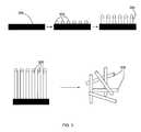
- FIG. 3is a schematic illustration of a typical nanowire synthesis process using a catalyst driven VLS process.
- FIGS. 4A-4Eschematically illustrates a process of synthesizing nanowires using a VLS method by employing inherent perturbations in a catalyst film on a substrate.
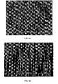
- FIG. 5Ais an SEM image of a 1.2 nm Au film showing that such film forms island clusters that can be used to nucleate nanowire growth.
- FIG. 5Bis an SEM image of a 5.0 nm Cr film showing larger diameter island clusters as compared to the thinner film of FIG. 5A .
- FIG. 5Cis a schematic representation of the film of FIG. 5B shown overlaying the film of FIG. 5A and illustrating how the islands of the overlying film mask selected island portions of the underlying film.
- FIG. 5Dshows the films of FIG. 5C following etching of exposed regions of the underlying film.
- FIG. 5Eshows removal of the overlying thin film following selective etching of the film.
- FIG. 5Fshows nanowire growth from the remaining catalyst islands of the underlying thin film.
- FIG. 6Ais an SEM image of a patterned Au film grown on a Si growth substrate prior to nanowire growth showing etched region 1100 that has been etched for about 5 seconds.
- FIG. 6Bis a 200 ⁇ magnified SEM image of the Au film of FIG. 6A showing that controlled etching of the Au film reduces the density of island clusters in the etched region by approximately a factor of ten versus the density of island clusters in the masked (e.g., non-etched) regions of the film.
- FIG. 6Cis an SEM image of the Au film of FIG. 6A after nanowire growth showing that nanowires grown in the etched regions of the Au film were found to be substantially oriented, and growth occurred without substantial background growth as compared to the other non-etched regions of the film.
- FIG. 6Dis a high-magnification SEM image of the Au film of FIG. 6C .
- nanowiresare frequently referred to, the techniques described herein are also applicable to other nanostructures, such as nanorods, nanotubes, nanotetrapods, nanoribbons and/or combinations thereof. It should further be appreciated that the manufacturing techniques described herein could be used to create any semiconductor device type, and other electronic component types. Further, the techniques would be suitable for application in electrical systems, optical systems, consumer electronics, industrial electronics, wireless systems, space applications, or any other application.
- an “aspect ratio”is the length of a first axis of a nanostructure divided by the average of the lengths of the second and third axes of the nanostructure, where the second and third axes are the two axes whose lengths are most nearly equal to each other.
- the aspect ratio for a perfect rodwould be the length of its long axis divided by the diameter of a cross-section perpendicular to (normal to) the long axis.
- heterostructurewhen used with reference to nanostructures refers to nanostructures characterized by at least two different and/or distinguishable material types. Typically, one region of the nanostructure comprises a first material type, while a second region of the nanostructure comprises a second material type.
- the nanostructurecomprises a core of a first material and at least one shell of a second (or third etc.) material, where the different material types are distributed radially about the long axis of a nanowire, a long axis of an arm of a branched nanocrystal, or the center of a nanocrystal, for example.
- a shellneed not completely cover the adjacent materials to be considered a shell or for the nanostructure to be considered a heterostructure.
- a nanocrystal characterized by a core of one material covered with small islands of a second materialis a heterostructure.
- the different material typesare distributed at different locations within the nanostructure.
- material typescan be distributed along the major (long) axis of a nanowire or along a long axis of arm of a branched nanocrystal.
- Different regions within a heterostructurecan comprise entirely different materials, or the different regions can comprise a base material.
- a “nanostructure”is a structure having at least one region or characteristic dimension with a dimension of less than about 500 nm, e.g., less than about 200 nm, less than about 100 nm, less than about 50 nm, or even less than about 20 nm. Typically, the region or characteristic dimension will be along the smallest axis of the structure. Examples of such structures include nanowires, nanorods, nanotubes, branched nanocrystals, nanotetrapods, tripods, bipods, nanocrystals, nanodots, quantum dots, nanoparticles, branched tetrapods (e.g., inorganic dendrimers), and the like.
- Nanostructurescan be substantially homogeneous in material properties, or in certain embodiments can be heterogeneous (e.g., heterostructures). Nanostructures can be, for example, substantially crystalline, substantially monocrystalline, polycrystalline, amorphous, or a combination thereof. In one aspect, each of the three dimensions of the nanostructure has a dimension of less than about 500 nm, for example, less than about 200 nm, less than about 100 nm, less than about 50 nm, or even less than about 20 nm.
- nanowiregenerally refers to any elongated conductive or semiconductive material (or other material described herein) that includes at least one cross sectional dimension that is less than 500 nm, and preferably, less than 100 nm, and has an aspect ratio (length:width) of greater than 10, preferably greater than 50, and more preferably, greater than 100.
- the nanowires of this inventioncan be substantially homogeneous in material properties, or in certain embodiments can be heterogeneous (e.g. nanowire heterostructures).
- the nanowirescan be fabricated from essentially any convenient material or materials, and can be, e.g., substantially crystalline, substantially monocrystalline, polycrystalline, or amorphous.
- Nanowirescan have a variable diameter or can have a substantially uniform diameter, that is, a diameter that shows a variance less than about 20% (e.g., less than about 10%, less than about 5%, or less than about 1%) over the region of greatest variability and over a linear dimension of at least 5 nm (e.g., at least 10 nm, at least 20 nm, or at least 50 nm).
- Nanowires according to this inventioncan expressly exclude carbon nanotubes, and, in certain embodiments, exclude “whiskers” or “nanowhiskers”, particularly whiskers having a diameter greater than 100 nm, or greater than about 200 nm.
- nanowiresexamples include semiconductor nanowires as described in Published International Patent Application Nos. WO 02/17362, WO 02/48701, and WO 01/03208, carbon nanotubes, and other elongated conductive or semiconductive structures of like dimensions, which are incorporated herein by reference.
- nanorodgenerally refers to any elongated conductive or semiconductive material (or other material described herein) similar to a nanowire, but having an aspect ratio (length:width) less than that of a nanowire.
- two or more nanorodscan be coupled together along their longitudinal axis so that the coupled nanorods span all the way between electrodes.
- two or more nanorodscan be substantially aligned along their longitudinal axis, but not coupled together, such that a small gap exists between the ends of the two or more nanorods.
- electronscan flow from one nanorod to another by hopping from one nanorod to another to traverse the small gap.
- the two or more nanorodscan be substantially aligned, such that they form a path by which electrons can travel between electrodes.
- a wide range of types of materials for nanowires, nanorods, nanotubes and nanoribbonscan be used, including semiconductor material selected from, e.g., Si, Ge, Sn, Se, Te, B, C (including diamond), P, B—C, B—P(BP 6 ), B—Si, Si—C, Si—Ge, Si—Sn and Ge—Sn, SiC, BN/BP/BAs, AlN/AlP/AlAs/AlSb, GaN/GaP/GaAs/GaSb, InN/InP/InAs/InSb, BN/BP/BAs, AlN/AlP/AlAs/AlSb, GaN/GaP/GaAs/GaSb, InN/InP/InAs/InSb, ZnO/ZnS/ZnSe/ZnTe, CdS/CdSe/CdTe, HgS/HgSe/Hg
- the nanowirescan also be formed from other materials such as metals such as gold, nickel, palladium, iradium, cobalt, chromium, aluminum, titanium, tin and the like, metal alloys, polymers, conductive polymers, ceramics, and/or combinations thereof.
- metalssuch as gold, nickel, palladium, iradium, cobalt, chromium, aluminum, titanium, tin and the like
- metal alloyspolymers, conductive polymers, ceramics, and/or combinations thereof.
- Other now known or later developed conducting or semiconductor materialscan be employed.
- the semiconductormay comprise a dopant from a group consisting of: a p-type dopant from Group III of the periodic table; an n-type dopant from Group V of the periodic table; a p-type dopant selected from a group consisting of: B, Al and In; an n-type dopant selected from a group consisting of: P, As and Sb; a p-type dopant from Group II of the periodic table; a p-type dopant selected from a group consisting of: Mg, Zn, Cd and Hg; a p-type dopant from Group IV of the periodic table; a p-type dopant selected from a group consisting of: C and Si; or an n-type dopant selected from a group consisting of: Si, Ge, Sn, S, Se and Te.
- Other now known or later developed dopant materialscan be employed.
- the nanowires or nanoribbonscan include carbon nanotubes, or nanotubes formed of conductive or semiconductive organic polymer materials, (e.g., pentacene, and transition metal oxides).
- conductive or semiconductive organic polymer materialse.g., pentacene, and transition metal oxides.
- Nanowiree.g., nanowire-like structures having a hollow tube formed axially therethrough.
- Nanotubescan be formed in combinations/thin films of nanotubes as is described herein for nanowires, alone or in combination with nanowires, to provide the properties and advantages described herein.
- Nanomaterialshave been produced in a wide variety of different ways. For example, solution based, surfactant mediated crystal growth has been described for producing spherical inorganic nanomaterials, e.g., quantum dots, as well as elongated nanomaterials, e.g., nanorods and nanotetrapods. Other methods have also been employed to produce nanomaterials, including vapor phase methods. For example, silicon nanocrystals have been reported produced by laser pyrolysis of silane gas.
- substrate based synthesis methodsincluding, e.g., low temperature synthesis methods for producing, e.g., ZnO nanowires as described by Greene et al. (“Low-temperature wafer scale production of ZnO nanowire arrays”, L. Greene, M. Law, J. Goldberger, F. Kim, J. Johnson, Y. Zhang, R. Saykally, P. Yang, Angew. Chem. Int. Ed. 42, 3031-3034, 2003), and higher temperature VLS methods that employ catalytic gold particles, e.g., that are deposited either as a colloid or as a thin film that forms a particle upon heating. Such VLS methods of producing nanowires are described in, for example, Published International Patent Application No. WO 02/017362, the full disclosure of which is incorporated herein by reference in its entirety for all purposes.
- FIG. 1Aillustrates a single crystal semiconductor nanowire core (hereafter “nanowire”) 100 .
- FIG. 1Ashows a nanowire 100 that is a uniformly doped single crystal nanowire.
- Such single crystal nanowirescan be doped into either p- or n-type semiconductors in a fairly controlled way.
- Doped nanowires such as nanowire 100exhibit improved electronic properties. For instance, such nanowires can be doped to have carrier mobility levels comparable to bulk single crystal materials.
- FIG. 1Bshows a nanowire 110 doped according to a core-shell structure.
- nanowire 110has a doped surface layer 112 , which can have varying thickness levels, including being only a molecular monolayer on the surface of nanowire 110 .
- the valence band of the insulating shellcan be lower than the valence band of the core for p-type doped wires, or the conduction band of the shell can be higher than the core for n-type doped wires.
- the core nanostructurecan be made from any metallic or semiconductor material, and the shell can be made from the same or a different material.
- the first core materialcan comprise a first semiconductor selected from the group consisting of: a Group II-VI semiconductor, a Group III-V semiconductor, a Group IV semiconductor, and an alloy thereof.
- the second material of the shellcan comprise a second semiconductor, the same as or different from the first semiconductor, e.g., selected from the group consisting of: a Group II-VI semiconductor, a Group III-V semiconductor, a Group IV semiconductor, and an alloy thereof.
- Example semiconductorsinclude, but are not limited to, CdSe, CdTe, InP, InAs, CdS, ZnS, ZnSe, ZnTe, HgTe, GaN, GaP, GaAs, GaSb, InSb, Si, Ge, AlAs, AlSb, PbSe, PbS, and PbTe.
- metallic materialssuch as gold, chromium, tin, nickel, aluminum etc. and alloys thereof can be used as the core material, and the metallic core can be overcoated with an appropriate shell material such as silicon dioxide or other insulating materials
- Nanostructurescan be fabricated and their size can be controlled by any of a number of convenient methods that can be adapted to different materials. For example, synthesis of nanocrystals of various composition is described in, e.g., Peng et al. (2000) “Shape Control of CdSe Nanocrystals” Nature 404, 59-61; Puntes et al. (2001) “Colloidal nanocrystal shape and size control: The case of cobalt” Science 291, 2115-2117; U.S. Pat. No. 6,306,736 to Alivisatos et al. (Oct. 23, 2001) entitled “Process for forming shaped group III-V semiconductor nanocrystals, and product formed using process”; U.S.
- nanowires having various aspect ratiosincluding nanowires with controlled diameters, is described in, e.g., Gudiksen et al (2000) “Diameter-selective synthesis of semiconductor nanowires” J. Am. Chem. Soc. 122, 8801-8802; Cui et al. (2001) “Diameter-controlled synthesis of single-crystal silicon nanowires” Appl. Phys. Lett. 78, 2214-2216; Gudiksen et al. (2001) “Synthetic control of the diameter and length of single crystal semiconductor nanowires” J. Phys. Chem. B 105,4062-4064; Morales et al.
- branched nanowirese.g., nanotetrapods, tripods, bipods, and branched tetrapods
- FIG. 1“Controlled synthesis of multi-armed CdS nanorod architectures using monosurfactant system” J. Am. Chem. Soc. 123, 5150-5151; and Manna et al. (2000) “ Synthesis of Soluble and Processable Rod - ,Arrow - , Teardrop - , and Tetrapod - Shaped CdSe Nanocrystals” J. Am. Chem. Soc. 122, 12700-12706.
- core-shell nanostructure heterostructuresnamely nanocrystal and nanowire (e.g., nanorod) core-shell heterostructures
- core-shell nanostructure heterostructuresnamely nanocrystal and nanowire (e.g., nanorod) core-shell heterostructures
- Peng et al.1997) “Epitaxial growth of highly luminescent CdSe/CdS core/shell nanocrystals with photostability and electronic accessibility” J. Am. Chem. Soc. 119, 7019-7029; Dabbousi et al. (1997) “(CdSe)ZnS core-shell quantum dots: Synthesis and characterization of a size series of highly luminescent nanocrysallites” J. Phys. Chem. B 101, 9463-9475; Manna et al.
- Nanowire heterostructuresin which the different materials are distributed at different locations along the long axis of the nanowire is described in, e.g., Gudiksen et al. (2002) “Growth of nanowire superlattice structures for nanoscale photonics and electronics” Nature 415, 617-620; Bjork et al. (2002) “One-dimensional steeplechase for electrons realized” Nano Letters 2, 86-90; Wu et al. (2002) “Block-by-block growth of single-crystalline Si/SiGe superlattice nanowires” Nano Letters 2, 83-86; and U.S. patent application 60/370,095 (Apr. 2, 2002) to Empedocles entitled “Nanowire heterostructures for encoding information.” Similar approaches can be applied to growth of other heterostructures.
- Exemplary applications of semiconductor nanowire materialsinclude simple electronic components, such as, transistors.
- a simple nanowire transistor deviceis shown in FIG. 2A .
- the basic device 200includes a source electrode 202 and a drain electrode 204 disposed upon a substrate 206 and spaced apart from each other.
- a semiconductor nanowire 208is provided spanning the two electrodes and is electrically connected to the electrodes 202 and 204 .
- the transistortypically includes an insulator or dielectric layer over its surface that provides insulation between the nanowire 208 and, for example, gate electrode 210 .
- the dielectric layeris provided as an oxide shell 212 or coating on the nanowire 208 .
- FETfield effect transistor
- FIG. 2Bschematically illustrates a variation of the simple device shown in FIG. 2A .
- the transistor device 250includes source 252 , drain 254 and gate 260 electrode provided upon a substrate 256 .
- a film or population of substantially oriented nanowires 258that span the source and drain electrodes 252 and 254 , bridging the gate electrode 260 .
- the nanowire film 258provides a much higher current density than a single nanowire based device, while retaining processibility advantages of film-based processing and uniformity.
- the fact that some of the nanowires in the nanowire population do not completely span the source and drain electrodesdoes not substantively affect the operation of the device as the overwhelming number of nanowires will provide this functionality.
- FIG. 3provides a schematic illustration of a typical nanowire synthesis process using a catalyst driven VLS process that is the basis from which a number of aspects of the present invention derive.
- a substrate 300is provided upon which nanowires will be synthesized.
- a population of catalytic particles 302for example, gold or other metal colloids, are then deposited upon the substrate surface.
- the particlesmay be provided as such, for example, as a population of colloidal particles, or they may be provided as a thin film on the substrate that is then formed into particles, for example, by heating and coalescence of the film.
- the substrate and particlesare then exposed to elevated temperatures, for example, from about 300° C. to 800° C., for example, about 600° C. to 800° C.
- a semiconductor precursor gasfor example, SiCl 4 .
- Other precursor gaseswill be known to individuals skilled in the relevant arts.
- super saturation of the metal particle with the semiconductorthen results in the crystallization of the semiconductor in a form that is defined by the diameter of the supersaturated particle, forming a cylindrical semiconductor wire 304 .
- the grown nanowiresare then harvested from the substrate to yield a population of free standing or suspended nanowires 308 .
- Certain aspects of the inventionare directed to improved processes for synthesizing nanowires from films of catalyst materials, for example, metallic films.
- this aspect of the inventionprovides for use of other types of films as the catalytic component for nanowire growth.
- Use of non-gold materialsprovides benefits of tunability of the overall process by providing variations in the properties of the film that is used, as well as provides benefits of lower cost, alternative nanowire composition, and altered processing parameters, for example, lower temperature melting point metal catalytic films for nanowire synthesis, for example, having a lower melting temperature than gold.
- low melting point metal filmsallows the use of a broader range of substrate materials including, for example, polymeric materials that have elevated melting temperatures, because such metals will tend to form eutectics with the semiconductor material being used for nanowire growth at lower temperatures, for example, temperatures less than about 400° C., and thus will not damage the underlying substrate.
- useful low melting temperature metalsinclude, for example, In, Cd, Sn, Zn, or alloys thereof, and the like.
- any metal that generate eutectics with the semiconductor material being used for nanowire growth at a temperature less than about 400° C.may be broadly useful in its applicability to alternative substrates, for example, polymers, conducting or non-conducting oxides, metal foils, etc., which substrates would otherwise be damaged during a typical CVD process.
- Such lower temperature processesmay optionally employ any of a variety of different nanowire materials, including, in addition to group IV semiconductors, group III-V semiconductors and their alloys, and those that form crystals at lower temperatures, for example, Group II-VI semiconductors and their alloys.
- group IV semiconductorsgroup III-V semiconductors and their alloys
- crystals at lower temperaturesfor example, Group II-VI semiconductors and their alloys.
- both low melting temperature and low temperature crystal synthesiswould be desired.
- the morphology of the filmsmay also be altered to adjust the properties of the wires synthesized therefrom.
- wire morphology resulting from metal film based growthis dependent, to some extent, upon the way in which the film melts, and coalesces during the heating/CVD process. Where larger droplets of metal catalyst form from the film, it will produce larger diameter wires, and vice versa.
- a filmwas patterned into predetermined sized islands or patches, which would coalesce into roughly equivalently sized droplets. However, this method would require some additional up-front processing steps to pattern the metal islands.
- break points in the coalescence pattern of the metal filmsmay be pre-designated to some extent by virtue of varying the film thickness over the surface, for example, during original deposition.
- the film thicknessmay be made thinner in certain regions and thicker in others, it will increase the probability that the coalescence breakage point, for example, where the film pulls apart from itself to form separate droplets, will form at such thinner regions, and the bulk of the droplet will be formed at the thicker regions.
- the correct function of periodically varying film thicknessesit may be possible to define not only the size of the formed droplets, but the location of their centers with accuracy that is greater than what could be achieved by simply patterning the location of catalyst islands as previously described.
- Generating relatively regular deviations in the film thicknessmay be accomplished by a number of methods. For example, in at least one embodiment, acoustic methods are used to impose a standing wave in a forming film that includes high spots and low spots across the wave. Orthogonally directed waves then optionally provide such variation in two dimensions. A variety of mechanisms can be employed in generating such high frequency waves across the film surface, including piezoelectric transducers, and the like, that can be placed into contact with the deposition substrate during metal film deposition.
- optical methodsmay be employed to impose standing wave pattern across a forming or melting metal film.
- Such optical methodstypically employ electromagnetic radiation, where the wavelength of the electromagnetic radiation defines the perturbation periodicity across the film surface.
- Orthogonally directed radiationcan define the pattern in two dimensions.
- mechanical methodsmay be used to define surface perturbations in a metal film to enhance uniform droplet formation.
- e-beam lithography, nano-imprint lithography, superlattice stamping, or the likemay be used to define high and low regions in a metal film. While also useful in generating uniform droplets for wire synthesis, such mechanical methods again require an additional processing step that adds to expense and complexity of wire production, and for that reason are less favored than the other methods described herein.
- surface perturbationsare imposed in a metal film, not as a result of a force exerted over the film, but as a result of the morphology of the underlying substrate.
- surface variations in an underlying substratemay impart a requisite variability to any overlaying metal layer to cause substantially regular coalescence patterns for the film upon heating.
- a polysilicon layeris provided that includes relatively regular grain boundaries between different crystal phases yielding a “stepping stone” morphology to the surface. When a film is deposited over these “stepping stones” the film will either form islands on each grain or have sufficient stresses at the grain boundary that upon heating, a pattern of coalescence will occur providing metal islands over the silicon grains.
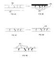
- a substrate 400may be provided with a deposited polysilicon layer 402 , as shown in FIG. 4A .
- Oxidation of the poly-Si layer 402provides an oxide 404 on the surface and at the grain boundaries 406 , as shown in FIG. 4B , which is subsequently etched away, as shown in FIG. 4C .
- the “stepping stone” morphologythen has a metal film 408 deposited thereon, as shown in FIG. 4D , which either directly forms metal islands 410 over the grain, or, upon heating, forms metal islands over the grain or boundary, based upon the differential stresses in each region, as shown in FIG. 4E .
- each of these metal islandsUpon exposure to the synthesis conditions, each of these metal islands then forms a catalytic particle that forms the basis for wire synthesis as described previously.
- This methodis similar to the patterned film methods described in Published International Patent Application No. WO 03/085700 (incorporated herein by reference in its entirety for all purposes), except that it relies upon the existing surface morphology of the underlying substrate as the patterning mechanism, as opposed to relying upon an additional patterning step.
- multiple layers of nano-thickness filmse.g., films having a thickness of less than about 10 nm
- one overlying film layeracts as a mask for exposing underlying film regions that can be selectively removed by etching, to provide isolated island regions of the underlying film that can be used to promote the growth of relatively clean, isolated, and substantially aligned nanowires by eliminating unwanted nanowire growth around the growing wires.
- FIG. 5Ais an SEM image of a 1.2 nm Au film showing that such film forms island clusters that can be used to nucleate nanowire growth.
- FIG. 5Bis an SEM image of a 5.0 nm Cr film showing larger diameter island clusters as compared to the thinner film of FIG. 5A .
- nano-thickness filmsform island clusters 500 and 502 that can be used as etch masks for lithography.
- Films with greater thicknessese.g., film in FIG. 5B having a thickness of about 5.0 nm
- tend to form larger island clusters 502 than those with relatively smaller thicknessese.g., as shown by the 1.2 nm thickness film of FIG. 5A ).
- FIG. 5Ashows that as shown in FIG.
- nano-thickness films on the order of about 5.0 nm in thicknesstend to produce island clusters 502 having an average diameter of between about 300 and 500 nm, while nano-thickness films having a thickness of about 1.2 nm tend to form island clusters 500 having an average diameter of between about 80 to 150 nm as shown in FIG. 5A .
- a first nano-thickness film of less than about 10 nm (for example, a 1.2 nm thick film as shown in FIG. 5A ) of a first catalyst material (e.g., Au)is deposited on a growth substrate 511 .
- the first filmis overlaid with at least one second thin film having the same or a different thickness (e.g., a film having a thickness of about 5.0 nm as shown in FIG. 5B ) than the first thin film.
- the second nano-thickness filmis made from a second material (e.g., Cr or other suitable material) from the first catalyst material so that the first and second films can be differentially etched. Both nanothickness films form island clusters 510 , 512 as shown in FIG. 5C when overlaid on top of one another.
- a second materiale.g., Cr or other suitable material
- an etchante.g., a wet etchant such as Transene TFA gold etchant (42% KI 3% I w/ balance in H 2 O)
- a wet etchantsuch as Transene TFA gold etchant (42% KI 3% I w/ balance in H 2 O)
- the island clusters 510 of the second thin filmserve as an etch mask for masking selected portions of the first thin film and exposing other portions of the film that can be selectively removed by etching.
- the second thin filmmay then optionally be removed by etching (e.g., using a Chromium wet etchant such as Cyantek CR-14) as shown in FIG. 5E .
- the remaining portions 512 of the first thin film not removed by etchingcan then be used to initiate nanowire growth.
- the first substrate and remaining portions of the first thin filmare heated to a temperature at which the first thin film melts.
- a semiconductore.g., Si for Si nanowires
- nanowire growthoccurs as catalyzed by the first catalyst material, to grow nanowires 514 at the site of the catalyst islands 512 , as shown in FIG. 5F .
- the final etched substratemay be coated with a colloid suspension of the first catalyst material (e.g., Au). If the colloid has an affinity for the remaining portions of the first thin film not removed by etching, but not the underlying substrate, these colloids will co-locate with the remaining portions of the first thin film.
- the first thin film and colloid compositemay then be used to initiate nanowire growth.
- the colloidshave an affinity for the underlying substrate, but not the remaining regions of the first thin-film not removed by etching, these colloids will co-locate with the exposed underlying substrate regions.
- the first thin-film and colloidsmay then be used to initiate nanowire growth simultaneously in different regions of the substrate.
- the first underlying thin filmmay be Au or Cr (or any other suitable metal or semiconductor (e.g., Si, Ge, etc.) film), and the second overlying, masking thin film may be Cr or Au (or any other suitable thin film).
- lower melting point metal films as described abovecan be used, such as In, Cd, Sn, Zn, or alloys thereof, and the like.
- any metal that generate eutectics with the semiconductor material being used for nanowire growth at a temperature less than about 400° C.may be broadly useful in its applicability to alternative substrates, for example, polymers, conducting or non-conducting oxides, metal foils, etc., can be used, which substrates would otherwise be damaged during a typical CVD process.
- Such lower temperature processesmay optionally employ any of a variety of different nanowire materials, including, in addition to group IV semiconductors, group III-V semiconductors, and those that form crystals as lower temperatures, e.g., Group II-VI semiconductors.
- the underlying film for initiating nanowire growthcan be a nano-thickness silicon film on a silicon-on-insulator (SOI) substrate, and a single nano-thickness film such as Au or Cr (or other suitable thin film) may be overlaid on the silicon film layer to mask selected regions of it.
- the exposed portions of the silicon film layer between the island clusters of the overlaying film layercan then be selectively removed by etching (e.g., using a silicon dry etching process) to leave selected portions of the underlying silicon film intact on the SOI substrate.
- the remaining portions of the silicon filmcan then be used to initiate nanowire growth (e.g., following wet etching to remove the overlying film layer).
- the inventionprovides a method for producing nanowires that comprises providing a patterned thin film of a catalyst material on a growth substrate, selected regions of the thin film are partially etched where nanowire growth is desired. A population of nanowires is then grown in the partially etched regions of the film.
- the filmis preferably a nano-thickness film of less than about 10 nm in thickness, for example between about 1 to about 7 nm in thickness, for example between about 1 and 5 nm in thickness.
- FIG. 6Ais a SEM image of a patterned Au film grown on a Si growth substrate prior to nanowire growth showing a rectangular-shaped etched region 600 that has been etched for about 5 seconds.
- the etched regionis created by wet etching selected patterned regions of the Au film using a gold wet etchant without any photolithography.
- FIG. 6Bis a 200 ⁇ magnified version of the Au film of FIG. 6A showing that controlled etching of the Au film reduces the density of island clusters 612 in the etched region by approximately a factor of ten versus the density of island clusters in the masked (e.g., non-etched) regions of the film on the left side of FIG. 6C .
- Numerous electronic devices and systemscan incorporate semiconductor or other type devices with thin films of nanowires produced by the methods of the present invention.
- Some example applications for the present inventionare described below or elsewhere herein for illustrative purposes, and are not limiting.
- the applications described hereincan include aligned or non-aligned thin films of nanowires, and can include composite or non-composite thin films of nanowires.
- Semiconductor devicescan be coupled to signals of other electronic circuits, and/or can be integrated with other electronic circuits.
- Semiconductor devicescan be formed on large substrates, which can be subsequently separated or diced into smaller substrates. Furthermore, on large substrates (i.e., substrates substantially larger than conventional semiconductor wafers), semiconductor devices formed thereon can be interconnected.
- the nanowires produced by the processes of the present inventioncan also be incorporated in applications requiring a single semiconductor device, and to multiple semiconductor devices.
- the nanowires produced by the processes of the present inventionare particularly applicable to large area, macro electronic substrates on which a plurality of semiconductor devices are formed.
- Such electronic devicescan include display driving circuits for active matrix liquid crystal displays (LCDs), organic LED displays, field emission displays.
- LCDsliquid crystal displays
- Other active displayscan be formed from a nanowire-polymer, quantum dots-polymer composite (the composite can function both as the emitter and active driving matrix).
- the nanowires produced by the processes of the present inventionare also applicable to smart libraries, credit cards, large area array sensors, and radio-frequency identification (RFID) tags, including smart cards, smart inventory tags, and the like.
- RFIDradio-frequency identification
- the nanowires produced by the processes of the present inventionare also applicable to digital and analog circuit applications.
- the nanowires produced by the processes of the present inventionare useful in applications that require ultra large-scale integration on a large area substrate.
- a thin film of nanowires produced by the processes of the present inventioncan be implemented in logic circuits, memory circuits, processors, amplifiers, and other digital and analog circuits.
- a clear conducting substrateis used to enhance the photovoltaic properties of the particular photovoltaic device.
- a clear conducting substratecan be used as a flexible, large-area replacement for indium tin oxide (ITO) or the like.
- ITOindium tin oxide
- a substratecan be coated with a thin film of nanowires that is formed to have a large bandgap, i.e., greater than visible light so that it would be non-absorbing, but would be formed to have either the HOMO or LUMO bands aligned with the active material of a photovoltaic device that would be formed on top of it.
- Clear conductorscan be located on two sides of the absorbing photovoltaic material to carry away current from the photovoltaic device.
- Two different nanowire materialscan be chosen, one having the HOMO aligned with that of the photovoltaic material HOMO band, and the other having the LUMO aligned with the LUMO band of the photovoltaic material.
- the bandgaps of the two nanowires materialscan be chosen to be much larger than that of the photovoltaic material.
- the nanowires, according to this embodimentcan be lightly doped to decrease the resistance of the thin films of nanowires, while permitting the substrate to remain mostly non-absorbing.
- such goodscan include personal computers, workstations, servers, networking devices, handheld electronic devices such as PDAs and palm pilots, telephones (e.g., cellular and standard), radios, televisions, electronic games and game systems, home security systems, automobiles, aircraft, boats, other household and commercial appliances, and the like.
- PDAs and palm pilotse.g., cellular and standard
- telephonese.g., cellular and standard
- radiose.g., televisions, electronic games and game systems, home security systems, automobiles, aircraft, boats, other household and commercial appliances, and the like.
Landscapes
- Engineering & Computer Science (AREA)
- Chemical & Material Sciences (AREA)
- Physics & Mathematics (AREA)
- Power Engineering (AREA)
- Computer Hardware Design (AREA)
- Microelectronics & Electronic Packaging (AREA)
- Manufacturing & Machinery (AREA)
- Condensed Matter Physics & Semiconductors (AREA)
- General Physics & Mathematics (AREA)
- Materials Engineering (AREA)
- Crystallography & Structural Chemistry (AREA)
- Nanotechnology (AREA)
- Metallurgy (AREA)
- Organic Chemistry (AREA)
- Mathematical Physics (AREA)
- Theoretical Computer Science (AREA)
- Thin Film Transistor (AREA)
- Crystals, And After-Treatments Of Crystals (AREA)
Abstract
Description
- The present application claims the benefit of the filing dates of U.S. Provisional Patent Application No. 60/586,170, filed Jul. 7, 2004, U.S. Provisional Patent Application No. 60/605,454, filed Aug. 30, 2004 and U.S. Provisional Patent Application No. 60/653,574, filed Feb. 16, 2005, the disclosures of which applications are incorporated by reference herein in their entireties.
- 1. Field of the Invention
- The present invention relates to nanowires, and more particularly, to nanowire growth.
- 2. Background of the Invention
- Nanomaterials, and in particular, nanowires have the potential to facilitate a whole new generation of electronic devices. For example, In certain cases, uses of nanomaterials have been proposed that exploit the unique and interesting properties of these materials more as a bulk material than as individual elements requiring individual assembly. For example, Duan et al.,Nature425:274-278 (September 2003), describes a nanowire based transistor for use in large area electronic substrates, such as, displays, antennas, and the like that employ a bulk processed, oriented semiconductor nanowire film or layer in place of a rigid semiconductor wafer. The result is an electronic substrate that performs on par with a single crystal wafer substrate that can be manufactured using conventional and less expensive processes than those used to manufacture poorer performing amorphous semiconductors, which is also more amenable to varied architectures, such as, flexible and/or shaped materials.
- In another example, bulk processed nanocrystals have been described for use as a flexible and efficient active layer for photoelectric devices. In particular, the ability to provide a quantum confined semiconductor crystal in a hole conducting matrix (to provide a type-II bandgap offset), allows the production of a photoactive layer that can be exploited either as a photovoltaic device or photoelectric detector. When disposed in an active composite, these nanomaterials are simply processed using standard film coating processes. See, e.g., U.S. patent application Ser. No. 10/656,802, filed Sep. 4, 2003, which is incorporated herein by reference in its entirety.
- In accordance with these uses of nanowires and other nanomaterials, the new process requirement is the ability to provide a film of nanowires that are substantially oriented along a given axis. The technology for such orientation has already been described in detail in, for example, International Publication Nos. WO 03/085700, WO 03/085701 and WO 2004/032191, as well as U.S. patent application Ser. No. 10/673,092, filed Sep. 25, 2003, which all are incorporated herein by reference in their entirety.
- A major impediment to the emergence of this new generation of electronic devices based on nanostructures is the ability to effectively grow nanowires and other nanostructures that have consistent characteristics. Current approaches to grow nanowires do not facilitate mass production, do not yield consistent nanowire performance characteristics and can be improved to generate better device performance based on nanowires.
- What are needed are systems and methods for growing nanowires that facilitate mass production, yield consistent nanowire performance characteristics and generate improved device performance.
- The present invention provides methods for growing nanowires that facilitate mass production, yield consistent nanowire performance characteristics and generate improved device performance. A primary benefit is the use of such materials in large area electronics applications.
- In a first aspect of the invention, the invention provides a method for producing nanowires, that comprises placing a thin film of a catalyst material on a substrate, the thin film having periodic thickness variations that include relatively thicker regions of the thin film and relatively thinner regions of the thin film. The substrate and thin film are heated to a temperature at which the thin film melts, whereupon the melting thin film disassociates from itself at the relatively thinner regions. A semiconductor is then vapor deposited onto the first substrate, and nanowire growth is catalyzed by the catalyst material.
- In another aspect of the invention, the invention provides a method for producing nanowires comprising providing thin film of a first catalyst material on a growth substrate, overlying the first thin film with at least one second thin film made from a second material different than the first catalyst material, the second thin film forming a plurality of islands on the first thin film. The first underlying thin film is selectively etched, such that a set of islands of the second thin film mask selected portions of the underlying first thin film and expose other regions of the first thin film that can be selectively removed by etching. A population of nanowires can then be grown on the first thin film.
- The second thin film may optionally be removed by etching (e.g., using a wet etchant) following etching of the selected regions of the first thin film. The remaining portions of the first thin film not removed by etching form islands that can then be used to nucleate nanowire growth. The growth substrate and first thin film are heated to a temperature at which the first thin film melts. Concurrently, a semiconductor is vapor deposited onto the first substrate, and nanowire growth is catalyzed by the first catalyst material.
- Additionally, the final etched substrate may be coated with a colloid suspension of the first catalyst material. If the colloid has an affinity for the remaining portions of the first thin film not removed by etching, but not the underlying substrate, these colloids will co-locate with the remaining portions of the first thin film. The first thin film and colloid composite can then be used to initiate nanowire growth. Alternatively, if the colloids have an affinity for the underlying substrate, but not the remaining regions of the first thin-film not removed by etching, these colloids will co-locate with the exposed underlying substrate regions. The first thin-film and colloids can then be used to initiate nanowire growth simultaneously in different regions of the substrate.
- The first thin film can be thinner than the second thin film, or alternatively the first thin film may be thicker than the second thin film. In one embodiment, the first thin film may be Au or Cr (or any other suitable metal catalytic film), and the second thin film may be Cr or Au (or any other suitable film that is preferably differentially etchable from the first thin film). Alternatively, a single thin film of material may be overlaid and form islands on a thin silicon layer on a silicon-on-insulator (SOI) substrate, and then the silicon layer etched (e.g., by dry etching) to leave selected portions of silicon on the SOI substrate. The thin silicon layer remaining on the substrate forms islands which can be used to nucleate nanowire wire.
- In another related aspect of the invention, the invention provides a method for producing nanowires that comprises providing a thin film of a catalyst material on a first substrate, the film forming a plurality of catalyst islands on the substrate of a first island density; partially etching one or more selected regions of the thin film where nanowire growth is desired leaving a subset of catalyst islands at a lower island density than the first density in the one or more regions; and growing a population of nanowires in the one or more partially etched regions from the remaining subset of catalyst islands. The thin film is preferably less than about 10 nm in thickness, for example between about 1 to about 7 nm in thickness, for example between about 1 and 5 nm in thickness. Such nano-thickness films form catalyst islands which can be used to nucleate the growth of nanowires. Controlled etching of selected regions of such films reduces the island density in those regions which enables the growth of isolated and substantially oriented nanowires while minimizing background growth in the etched regions, thus simplifying post-growth processing of the wires.
- Further embodiments, features, and advantages of the invention, as well as the structure and operation of the various embodiments of the invention are described in detail below with reference to accompanying drawings.
- The invention is described with reference to the accompanying drawings. In the drawings, like reference numbers indicate identical or functionally similar elements. The drawing in which an element first appears is indicated by the left-most digit in the corresponding reference number.
FIG. 1A is a diagram of a single crystal semiconductor nanowire.FIG. 1B is a diagram of a nanowire doped according to a core-shell structure.FIG. 2A is a diagram of a nanowire based transistor device.FIG. 2B is a diagram of a nanowire based transistor device having a film of oriented nanowires employed as the conductive channel.FIG. 3 is a schematic illustration of a typical nanowire synthesis process using a catalyst driven VLS process.FIGS. 4A-4E schematically illustrates a process of synthesizing nanowires using a VLS method by employing inherent perturbations in a catalyst film on a substrate.FIG. 5A is an SEM image of a 1.2 nm Au film showing that such film forms island clusters that can be used to nucleate nanowire growth.FIG. 5B is an SEM image of a 5.0 nm Cr film showing larger diameter island clusters as compared to the thinner film ofFIG. 5A .FIG. 5C is a schematic representation of the film ofFIG. 5B shown overlaying the film ofFIG. 5A and illustrating how the islands of the overlying film mask selected island portions of the underlying film.FIG. 5D shows the films ofFIG. 5C following etching of exposed regions of the underlying film.FIG. 5E shows removal of the overlying thin film following selective etching of the film.FIG. 5F shows nanowire growth from the remaining catalyst islands of the underlying thin film.FIG. 6A is an SEM image of a patterned Au film grown on a Si growth substrate prior to nanowire growth showing etched region1100 that has been etched for about 5 seconds.FIG. 6B is a 200× magnified SEM image of the Au film ofFIG. 6A showing that controlled etching of the Au film reduces the density of island clusters in the etched region by approximately a factor of ten versus the density of island clusters in the masked (e.g., non-etched) regions of the film.FIG. 6C is an SEM image of the Au film ofFIG. 6A after nanowire growth showing that nanowires grown in the etched regions of the Au film were found to be substantially oriented, and growth occurred without substantial background growth as compared to the other non-etched regions of the film.FIG. 6D is a high-magnification SEM image of the Au film ofFIG. 6C .- It should be appreciated that the particular implementations shown and described herein are examples of the invention and are not intended to otherwise limit the scope of the present invention in any way. Indeed, for the sake of brevity, conventional electronics, manufacturing, semiconductor devices, and nanowire (NW), nanorod, nanotube, and nanoribbon technologies and other functional aspects of the systems (and components of the individual operating components of the systems) may not be described in detail herein. Furthermore, for purposes of brevity, the invention is frequently described herein as pertaining to nanowires.
- It should be appreciated that although nanowires are frequently referred to, the techniques described herein are also applicable to other nanostructures, such as nanorods, nanotubes, nanotetrapods, nanoribbons and/or combinations thereof. It should further be appreciated that the manufacturing techniques described herein could be used to create any semiconductor device type, and other electronic component types. Further, the techniques would be suitable for application in electrical systems, optical systems, consumer electronics, industrial electronics, wireless systems, space applications, or any other application.
- As used herein, an “aspect ratio” is the length of a first axis of a nanostructure divided by the average of the lengths of the second and third axes of the nanostructure, where the second and third axes are the two axes whose lengths are most nearly equal to each other. For example, the aspect ratio for a perfect rod would be the length of its long axis divided by the diameter of a cross-section perpendicular to (normal to) the long axis.
- The term “heterostructure” when used with reference to nanostructures refers to nanostructures characterized by at least two different and/or distinguishable material types. Typically, one region of the nanostructure comprises a first material type, while a second region of the nanostructure comprises a second material type. In certain embodiments, the nanostructure comprises a core of a first material and at least one shell of a second (or third etc.) material, where the different material types are distributed radially about the long axis of a nanowire, a long axis of an arm of a branched nanocrystal, or the center of a nanocrystal, for example. A shell need not completely cover the adjacent materials to be considered a shell or for the nanostructure to be considered a heterostructure. For example, a nanocrystal characterized by a core of one material covered with small islands of a second material is a heterostructure. In other embodiments, the different material types are distributed at different locations within the nanostructure. For example, material types can be distributed along the major (long) axis of a nanowire or along a long axis of arm of a branched nanocrystal. Different regions within a heterostructure can comprise entirely different materials, or the different regions can comprise a base material.
- As used herein, a “nanostructure” is a structure having at least one region or characteristic dimension with a dimension of less than about 500 nm, e.g., less than about 200 nm, less than about 100 nm, less than about 50 nm, or even less than about 20 nm. Typically, the region or characteristic dimension will be along the smallest axis of the structure. Examples of such structures include nanowires, nanorods, nanotubes, branched nanocrystals, nanotetrapods, tripods, bipods, nanocrystals, nanodots, quantum dots, nanoparticles, branched tetrapods (e.g., inorganic dendrimers), and the like. Nanostructures can be substantially homogeneous in material properties, or in certain embodiments can be heterogeneous (e.g., heterostructures). Nanostructures can be, for example, substantially crystalline, substantially monocrystalline, polycrystalline, amorphous, or a combination thereof. In one aspect, each of the three dimensions of the nanostructure has a dimension of less than about 500 nm, for example, less than about 200 nm, less than about 100 nm, less than about 50 nm, or even less than about 20 nm.
- As used herein, the term “nanowire” generally refers to any elongated conductive or semiconductive material (or other material described herein) that includes at least one cross sectional dimension that is less than 500 nm, and preferably, less than 100 nm, and has an aspect ratio (length:width) of greater than 10, preferably greater than 50, and more preferably, greater than 100.
- The nanowires of this invention can be substantially homogeneous in material properties, or in certain embodiments can be heterogeneous (e.g. nanowire heterostructures). The nanowires can be fabricated from essentially any convenient material or materials, and can be, e.g., substantially crystalline, substantially monocrystalline, polycrystalline, or amorphous. Nanowires can have a variable diameter or can have a substantially uniform diameter, that is, a diameter that shows a variance less than about 20% (e.g., less than about 10%, less than about 5%, or less than about 1%) over the region of greatest variability and over a linear dimension of at least 5 nm (e.g., at least 10 nm, at least 20 nm, or at least 50 nm). Typically the diameter is evaluated away from the ends of the nanowire (e.g. over the central 20%, 40%, 50%, or 80% of the nanowire). A nanowire can be straight or can be e.g. curved or bent, over the entire length of its long axis or a portion thereof. In certain embodiments, a nanowire or a portion thereof can exhibit two- or three-dimensional quantum confinement. Nanowires according to this invention can expressly exclude carbon nanotubes, and, in certain embodiments, exclude “whiskers” or “nanowhiskers”, particularly whiskers having a diameter greater than 100 nm, or greater than about 200 nm.
- Examples of such nanowires include semiconductor nanowires as described in Published International Patent Application Nos. WO 02/17362, WO 02/48701, and WO 01/03208, carbon nanotubes, and other elongated conductive or semiconductive structures of like dimensions, which are incorporated herein by reference.
- As used herein, the term “nanorod” generally refers to any elongated conductive or semiconductive material (or other material described herein) similar to a nanowire, but having an aspect ratio (length:width) less than that of a nanowire. Note that two or more nanorods can be coupled together along their longitudinal axis so that the coupled nanorods span all the way between electrodes. Alternatively, two or more nanorods can be substantially aligned along their longitudinal axis, but not coupled together, such that a small gap exists between the ends of the two or more nanorods. In this case, electrons can flow from one nanorod to another by hopping from one nanorod to another to traverse the small gap. The two or more nanorods can be substantially aligned, such that they form a path by which electrons can travel between electrodes.
- A wide range of types of materials for nanowires, nanorods, nanotubes and nanoribbons can be used, including semiconductor material selected from, e.g., Si, Ge, Sn, Se, Te, B, C (including diamond), P, B—C, B—P(BP6), B—Si, Si—C, Si—Ge, Si—Sn and Ge—Sn, SiC, BN/BP/BAs, AlN/AlP/AlAs/AlSb, GaN/GaP/GaAs/GaSb, InN/InP/InAs/InSb, BN/BP/BAs, AlN/AlP/AlAs/AlSb, GaN/GaP/GaAs/GaSb, InN/InP/InAs/InSb, ZnO/ZnS/ZnSe/ZnTe, CdS/CdSe/CdTe, HgS/HgSe/HgTe, BeS/BeSe/BeTe/MgS/MgSe, GeS, GeSe, GeTe, SnS, SnSe, SnTe, PbO, PbS, PbSe, PbTe, CuF, CuCl, CuBr, CuI, AgF, AgCl, AgBr, AgI, BeSiN2, CaCN2, ZnGeP2, CdSnAs2, ZnSnSb2, CuGeP3, CuSi2P3, (Cu, Ag)(Al, Ga, In, Ti, Fe)(S, Se, Te)2, Si3N4, Ge3N4, Al2O3, (Al, Ga, In)2(S, Se, Te)3, Al2CO, and an appropriate combination of two or more such semiconductors.
- The nanowires can also be formed from other materials such as metals such as gold, nickel, palladium, iradium, cobalt, chromium, aluminum, titanium, tin and the like, metal alloys, polymers, conductive polymers, ceramics, and/or combinations thereof. Other now known or later developed conducting or semiconductor materials can be employed.
- In certain aspects, the semiconductor may comprise a dopant from a group consisting of: a p-type dopant from Group III of the periodic table; an n-type dopant from Group V of the periodic table; a p-type dopant selected from a group consisting of: B, Al and In; an n-type dopant selected from a group consisting of: P, As and Sb; a p-type dopant from Group II of the periodic table; a p-type dopant selected from a group consisting of: Mg, Zn, Cd and Hg; a p-type dopant from Group IV of the periodic table; a p-type dopant selected from a group consisting of: C and Si; or an n-type dopant selected from a group consisting of: Si, Ge, Sn, S, Se and Te. Other now known or later developed dopant materials can be employed.
- Additionally, the nanowires or nanoribbons can include carbon nanotubes, or nanotubes formed of conductive or semiconductive organic polymer materials, (e.g., pentacene, and transition metal oxides).
- Hence, although the term “nanowire” is referred to throughout the description herein for illustrative purposes, it is intended that the description herein also encompass the use of nanotubes (e.g., nanowire-like structures having a hollow tube formed axially therethrough). Nanotubes can be formed in combinations/thin films of nanotubes as is described herein for nanowires, alone or in combination with nanowires, to provide the properties and advantages described herein.
- It should be understood that the spatial descriptions (e.g., “above”, “below”, “up”, “down”, “top”, “bottom”, etc.) made herein are for purposes of illustration only, and that devices of the present invention can be spatially arranged in any orientation or manner.
- Nanomaterials have been produced in a wide variety of different ways. For example, solution based, surfactant mediated crystal growth has been described for producing spherical inorganic nanomaterials, e.g., quantum dots, as well as elongated nanomaterials, e.g., nanorods and nanotetrapods. Other methods have also been employed to produce nanomaterials, including vapor phase methods. For example, silicon nanocrystals have been reported produced by laser pyrolysis of silane gas.
- Other methods employ substrate based synthesis methods including, e.g., low temperature synthesis methods for producing, e.g., ZnO nanowires as described by Greene et al. (“Low-temperature wafer scale production of ZnO nanowire arrays”, L. Greene, M. Law, J. Goldberger, F. Kim, J. Johnson, Y. Zhang, R. Saykally, P. Yang, Angew.Chem. Int. Ed.42, 3031-3034, 2003), and higher temperature VLS methods that employ catalytic gold particles, e.g., that are deposited either as a colloid or as a thin film that forms a particle upon heating. Such VLS methods of producing nanowires are described in, for example, Published International Patent Application No. WO 02/017362, the full disclosure of which is incorporated herein by reference in its entirety for all purposes.
- Types of Nanowires and Their Synthesis
FIG. 1A illustrates a single crystal semiconductor nanowire core (hereafter “nanowire”)100.FIG. 1A shows ananowire 100 that is a uniformly doped single crystal nanowire. Such single crystal nanowires can be doped into either p- or n-type semiconductors in a fairly controlled way. Doped nanowires such asnanowire 100 exhibit improved electronic properties. For instance, such nanowires can be doped to have carrier mobility levels comparable to bulk single crystal materials.FIG. 1B shows ananowire 110 doped according to a core-shell structure. As shown inFIG. 1B ,nanowire 110 has a dopedsurface layer 112, which can have varying thickness levels, including being only a molecular monolayer on the surface ofnanowire 110.- The valence band of the insulating shell can be lower than the valence band of the core for p-type doped wires, or the conduction band of the shell can be higher than the core for n-type doped wires. Generally, the core nanostructure can be made from any metallic or semiconductor material, and the shell can be made from the same or a different material. For example, the first core material can comprise a first semiconductor selected from the group consisting of: a Group II-VI semiconductor, a Group III-V semiconductor, a Group IV semiconductor, and an alloy thereof. Similarly, the second material of the shell can comprise a second semiconductor, the same as or different from the first semiconductor, e.g., selected from the group consisting of: a Group II-VI semiconductor, a Group III-V semiconductor, a Group IV semiconductor, and an alloy thereof. Example semiconductors include, but are not limited to, CdSe, CdTe, InP, InAs, CdS, ZnS, ZnSe, ZnTe, HgTe, GaN, GaP, GaAs, GaSb, InSb, Si, Ge, AlAs, AlSb, PbSe, PbS, and PbTe. As noted above, metallic materials such as gold, chromium, tin, nickel, aluminum etc. and alloys thereof can be used as the core material, and the metallic core can be overcoated with an appropriate shell material such as silicon dioxide or other insulating materials
- Nanostructures can be fabricated and their size can be controlled by any of a number of convenient methods that can be adapted to different materials. For example, synthesis of nanocrystals of various composition is described in, e.g., Peng et al. (2000) “Shape Control of CdSe Nanocrystals”
Nature 404, 59-61; Puntes et al. (2001) “Colloidal nanocrystal shape and size control: The case of cobalt”Science291, 2115-2117; U.S. Pat. No. 6,306,736 to Alivisatos et al. (Oct. 23, 2001) entitled “Process for forming shaped group III-V semiconductor nanocrystals, and product formed using process”; U.S. Pat. No. 6,225,198 to Alivisatos et al. (May 1, 2001) entitled “Process for forming shaped group II-VI semiconductor nanocrystals, and product formed using process”; U.S. Pat. No. 5,505,928 to Alivisatos et al. (Apr. 9, 1996) entitled “Preparation of III-V semiconductor nanocrystals”; U.S. Pat. No. 5,751,018 to Alivisatos et al. (May 12, 1998) entitled “Semiconductor nanocrystals covalently bound to solid inorganic surfaces using self-assembled monolayers”; U.S. Pat. No. 6,048,616 to Gallagher et al. (Apr. 11, 2000) entitled “Encapsulated quantum sized doped semiconductor particles and method of manufacturing same”; and U.S. Pat. No. 5,990,479 to Weiss et al. (Nov. 23, 1999) entitled “Organo luminescent semiconductor nanocrystal probes for biological applications and process for making and using such probes.” - Growth of nanowires having various aspect ratios, including nanowires with controlled diameters, is described in, e.g., Gudiksen et al (2000) “Diameter-selective synthesis of semiconductor nanowires”J. Am. Chem. Soc.122, 8801-8802; Cui et al. (2001) “Diameter-controlled synthesis of single-crystal silicon nanowires”Appl. Phys. Lett.78, 2214-2216; Gudiksen et al. (2001) “Synthetic control of the diameter and length of single crystal semiconductor nanowires”J. Phys. Chem. B105,4062-4064; Morales et al. (1998) “A laser ablation method for the synthesis of crystalline semiconductor nanowires”Science279, 208-211; Duan et al. (2000) “General synthesis of compound semiconductor nanowires”Adv. Mater.12, 298-302; Cui et al. (2000) “Doping and electrical transport in silicon nanowires”J. Phys. Chem. B104, 5213-5216; Peng et al. (2000) “Shape control of CdSe nanocrystals”
Nature 404, 59-61; Puntes et al. (2001) “Colloidal nanocrystal shape and size control: The case of cobalt”Science291, 2115-2117; U.S. Pat. No. 6,306,736 to Alivisatos et al. (Oct. 23, 2001) entitled “Process for forming shaped group III-V semiconductor nanocrystals, and product formed using process”; U.S. Pat. No. 6,225,198 to Alivisatos et al. (May 1, 2001) entitled “Process for forming shaped group II-VI semiconductor nanocrystals, and product formed using process”; U.S. Pat. No. 6,036,774 to Lieber et al. (Mar. 14, 2000) entitled “Method of producing metal oxide nanorods”; U.S. Pat. No. 5,897,945 to Lieber et al. (Apr. 27, 1999) entitled “Metal oxide nanorods”; U.S. Pat. No. 5,997,832 to Lieber et al. (Dec. 7, 1999) “Preparation of carbide nanorods”; Urbau et al. (2002) “Synthesis of single-crystalline perovskite nanowires composed of barium titanate and strontium titanate”J. Am. Chem. Soc.,124, 1186; and Yun et al. (2002) “Ferroelectric Properties of Individual Barium Titanate Nanowires Investigated by Scanned Probe Microscopy”Nanoletters2, 447. - Growth of branched nanowires (e.g., nanotetrapods, tripods, bipods, and branched tetrapods) is described in, e.g., Jun et al. (2001) “Controlled synthesis of multi-armed CdS nanorod architectures using monosurfactant system”J. Am. Chem. Soc.123, 5150-5151; and Manna et al. (2000) “Synthesis of Soluble and Processable Rod-,Arrow-, Teardrop-, and Tetrapod-Shaped CdSe Nanocrystals” J. Am. Chem. Soc.122, 12700-12706.
- Synthesis of nanoparticles is described in, e.g., U.S. Pat. No. 5,690,807 to Clark Jr. et al. (Nov. 25, 1997) entitled “Method for producing semiconductor particles”; U.S. Pat. No. 6,136,156 to El-Shall, et al. (Oct. 24, 2000) entitled “Nanoparticles of silicon oxide alloys”; U.S. Pat. No. 6,413,489 to Ying et al. (Jul. 2, 2002) entitled “Synthesis of nanometer-sized particles by reverse micelle mediated techniques”; and Liu et al. (2001) “Sol-Gel Synthesis of Free-Standing Ferroelectric Lead Zirconate Titanate Nanoparticles”J. Am. Chem. Soc.123, 4344. Synthesis of nanoparticles is also described in the above citations for growth of nanocrystals, nanowires, and branched nanowires, where the resulting nanostructures have an aspect ratio less than about 1.5.
- Synthesis of core-shell nanostructure heterostructures, namely nanocrystal and nanowire (e.g., nanorod) core-shell heterostructures, are described in, e.g., Peng et al. (1997) “Epitaxial growth of highly luminescent CdSe/CdS core/shell nanocrystals with photostability and electronic accessibility”J. Am. Chem. Soc.119, 7019-7029; Dabbousi et al. (1997) “(CdSe)ZnS core-shell quantum dots: Synthesis and characterization of a size series of highly luminescent nanocrysallites”J. Phys. Chem. B101, 9463-9475; Manna et al. (2002) “Epitaxial growth and photochemical annealing of graded CdS/ZnS shells on colloidal CdSe nanorods” J. Am. Chem. Soc.124, 7136-7145; and Cao et al. (2000) “Growth and properties of semiconductor core/shell nanocrystals with InAs cores”J. Am. Chem. Soc.122, 9692-9702. Similar approaches can be applied to growth of other core-shell nanostructures.
- Growth of nanowire heterostructures in which the different materials are distributed at different locations along the long axis of the nanowire is described in, e.g., Gudiksen et al. (2002) “Growth of nanowire superlattice structures for nanoscale photonics and electronics”Nature415, 617-620; Bjork et al. (2002) “One-dimensional steeplechase for electrons realized”Nano Letters2, 86-90; Wu et al. (2002) “Block-by-block growth of single-crystalline Si/SiGe superlattice nanowires”Nano Letters2, 83-86; and U.S. patent application 60/370,095 (Apr. 2, 2002) to Empedocles entitled “Nanowire heterostructures for encoding information.” Similar approaches can be applied to growth of other heterostructures.
- Exemplary Nanowire Devices
- Exemplary applications of semiconductor nanowire materials include simple electronic components, such as, transistors. For example, a simple nanowire transistor device is shown in
FIG. 2A . As shown, thebasic device 200 includes asource electrode 202 and adrain electrode 204 disposed upon asubstrate 206 and spaced apart from each other. Asemiconductor nanowire 208 is provided spanning the two electrodes and is electrically connected to theelectrodes nanowire 208 and, for example,gate electrode 210. As shown, the dielectric layer is provided as anoxide shell 212 or coating on thenanowire 208. By modulating the field applied to thegate electrode 210, one can vary the conductivity of thenanowire 208 as in a conventional field effect transistor (FET). FIG. 2B schematically illustrates a variation of the simple device shown inFIG. 2A . As shown, thetransistor device 250 includessource 252, drain254 andgate 260 electrode provided upon asubstrate 256. However, in place of a single nanowire with a dielectric shell is a film or population of substantially orientednanowires 258 that span the source and drainelectrodes gate electrode 260. As compared to the device illustrated inFIG. 2A , thenanowire film 258 provides a much higher current density than a single nanowire based device, while retaining processibility advantages of film-based processing and uniformity. In particular, the fact that some of the nanowires in the nanowire population do not completely span the source and drain electrodes does not substantively affect the operation of the device as the overwhelming number of nanowires will provide this functionality.- Growth of Nanowires from Films
FIG. 3 provides a schematic illustration of a typical nanowire synthesis process using a catalyst driven VLS process that is the basis from which a number of aspects of the present invention derive. Briefly, as shown, asubstrate 300 is provided upon which nanowires will be synthesized. A population ofcatalytic particles 302, for example, gold or other metal colloids, are then deposited upon the substrate surface. The particles may be provided as such, for example, as a population of colloidal particles, or they may be provided as a thin film on the substrate that is then formed into particles, for example, by heating and coalescence of the film. The substrate and particles are then exposed to elevated temperatures, for example, from about 300° C. to 800° C., for example, about 600° C. to 800° C. in the presence of a semiconductor precursor gas, for example, SiCl4. Other precursor gases will be known to individuals skilled in the relevant arts. Super saturation of the metal particle with the semiconductor then results in the crystallization of the semiconductor in a form that is defined by the diameter of the supersaturated particle, forming acylindrical semiconductor wire 304. Continued growth then elongates the nanowire untilwires 306 of a desired length are achieved. For many applications, the grown nanowires are then harvested from the substrate to yield a population of free standing or suspendednanowires 308.- Certain aspects of the invention are directed to improved processes for synthesizing nanowires from films of catalyst materials, for example, metallic films. In particular, in contrast to previously described processes, this aspect of the invention provides for use of other types of films as the catalytic component for nanowire growth. Use of non-gold materials provides benefits of tunability of the overall process by providing variations in the properties of the film that is used, as well as provides benefits of lower cost, alternative nanowire composition, and altered processing parameters, for example, lower temperature melting point metal catalytic films for nanowire synthesis, for example, having a lower melting temperature than gold. Use of low melting point metal films allows the use of a broader range of substrate materials including, for example, polymeric materials that have elevated melting temperatures, because such metals will tend to form eutectics with the semiconductor material being used for nanowire growth at lower temperatures, for example, temperatures less than about 400° C., and thus will not damage the underlying substrate.
- Examples of useful low melting temperature metals include, for example, In, Cd, Sn, Zn, or alloys thereof, and the like. Typically, any metal that generate eutectics with the semiconductor material being used for nanowire growth at a temperature less than about 400° C., may be broadly useful in its applicability to alternative substrates, for example, polymers, conducting or non-conducting oxides, metal foils, etc., which substrates would otherwise be damaged during a typical CVD process. Such lower temperature processes may optionally employ any of a variety of different nanowire materials, including, in addition to group IV semiconductors, group III-V semiconductors and their alloys, and those that form crystals at lower temperatures, for example, Group II-VI semiconductors and their alloys. Of course, as will be appreciated, where lower temperature synthesis is desired, for example, to preserve the properties of the underlying substrate, both low melting temperature and low temperature crystal synthesis would be desired.
- In addition to using films of different compositions, the morphology of the films may also be altered to adjust the properties of the wires synthesized therefrom. In particular, wire morphology resulting from metal film based growth is dependent, to some extent, upon the way in which the film melts, and coalesces during the heating/CVD process. Where larger droplets of metal catalyst form from the film, it will produce larger diameter wires, and vice versa. In other processes, a film was patterned into predetermined sized islands or patches, which would coalesce into roughly equivalently sized droplets. However, this method would require some additional up-front processing steps to pattern the metal islands.
- Accordingly, in certain aspects of the invention, break points in the coalescence pattern of the metal films may be pre-designated to some extent by virtue of varying the film thickness over the surface, for example, during original deposition. In particular, by making the film thinner in certain regions and thicker in others, it will increase the probability that the coalescence breakage point, for example, where the film pulls apart from itself to form separate droplets, will form at such thinner regions, and the bulk of the droplet will be formed at the thicker regions. In fact, with the correct function of periodically varying film thicknesses, it may be possible to define not only the size of the formed droplets, but the location of their centers with accuracy that is greater than what could be achieved by simply patterning the location of catalyst islands as previously described.
- Generating relatively regular deviations in the film thickness may be accomplished by a number of methods. For example, in at least one embodiment, acoustic methods are used to impose a standing wave in a forming film that includes high spots and low spots across the wave. Orthogonally directed waves then optionally provide such variation in two dimensions. A variety of mechanisms can be employed in generating such high frequency waves across the film surface, including piezoelectric transducers, and the like, that can be placed into contact with the deposition substrate during metal film deposition.
- In related aspects, optical methods may be employed to impose standing wave pattern across a forming or melting metal film. Such optical methods typically employ electromagnetic radiation, where the wavelength of the electromagnetic radiation defines the perturbation periodicity across the film surface. Orthogonally directed radiation can define the pattern in two dimensions.
- In a further variation, mechanical methods may be used to define surface perturbations in a metal film to enhance uniform droplet formation. In particular, e-beam lithography, nano-imprint lithography, superlattice stamping, or the like, may be used to define high and low regions in a metal film. While also useful in generating uniform droplets for wire synthesis, such mechanical methods again require an additional processing step that adds to expense and complexity of wire production, and for that reason are less favored than the other methods described herein.
- In another aspect, surface perturbations are imposed in a metal film, not as a result of a force exerted over the film, but as a result of the morphology of the underlying substrate. In particular, surface variations in an underlying substrate may impart a requisite variability to any overlaying metal layer to cause substantially regular coalescence patterns for the film upon heating. In at least a first example, a polysilicon layer is provided that includes relatively regular grain boundaries between different crystal phases yielding a “stepping stone” morphology to the surface. When a film is deposited over these “stepping stones” the film will either form islands on each grain or have sufficient stresses at the grain boundary that upon heating, a pattern of coalescence will occur providing metal islands over the silicon grains.
- In practice, and as shown in
FIGS. 4A-4E , asubstrate 400 may be provided with a depositedpolysilicon layer 402, as shown inFIG. 4A . Oxidation of the poly-Si layer 402 provides anoxide 404 on the surface and at thegrain boundaries 406, as shown inFIG. 4B , which is subsequently etched away, as shown inFIG. 4C . The “stepping stone” morphology then has ametal film 408 deposited thereon, as shown inFIG. 4D , which either directly formsmetal islands 410 over the grain, or, upon heating, forms metal islands over the grain or boundary, based upon the differential stresses in each region, as shown inFIG. 4E . Upon exposure to the synthesis conditions, each of these metal islands then forms a catalytic particle that forms the basis for wire synthesis as described previously. This method is similar to the patterned film methods described in Published International Patent Application No. WO 03/085700 (incorporated herein by reference in its entirety for all purposes), except that it relies upon the existing surface morphology of the underlying substrate as the patterning mechanism, as opposed to relying upon an additional patterning step. - In another aspect of the invention, multiple layers of nano-thickness films (e.g., films having a thickness of less than about 10 nm) can be used wherein one overlying film layer acts as a mask for exposing underlying film regions that can be selectively removed by etching, to provide isolated island regions of the underlying film that can be used to promote the growth of relatively clean, isolated, and substantially aligned nanowires by eliminating unwanted nanowire growth around the growing wires.
FIG. 5A is an SEM image of a 1.2 nm Au film showing that such film forms island clusters that can be used to nucleate nanowire growth.FIG. 5B is an SEM image of a 5.0 nm Cr film showing larger diameter island clusters as compared to the thinner film ofFIG. 5A .- As shown for example in FIGS.5A-B, nano-thickness films form
island clusters FIG. 5B having a thickness of about 5.0 nm) tend to formlarger island clusters 502 than those with relatively smaller thicknesses (e.g., as shown by the 1.2 nm thickness film ofFIG. 5A ). For example, as shown inFIG. 5B , nano-thickness films on the order of about 5.0 nm in thickness tend to produceisland clusters 502 having an average diameter of between about 300 and 500 nm, while nano-thickness films having a thickness of about 1.2 nm tend to formisland clusters 500 having an average diameter of between about 80 to 150 nm as shown inFIG. 5A . - Based on this understanding, and as shown with reference to FIGS.5C-F, in this aspect of the invention, a first nano-thickness film of less than about 10 nm (for example, a 1.2 nm thick film as shown in
FIG. 5A ) of a first catalyst material (e.g., Au) is deposited on agrowth substrate 511. Then the first film is overlaid with at least one second thin film having the same or a different thickness (e.g., a film having a thickness of about 5.0 nm as shown inFIG. 5B ) than the first thin film. The second nano-thickness film is made from a second material (e.g., Cr or other suitable material) from the first catalyst material so that the first and second films can be differentially etched. Both nanothickness films formisland clusters FIG. 5C when overlaid on top of one another. - As shown in
FIG. 5D , an etchant (e.g., a wet etchant such as Transene TFA gold etchant (42% KI 3% I w/ balance in H2O)) is then used to selectively etch the first underlying thin film (e.g., Au) to remove selected exposed regions of it from thegrowth substrate 511. Theisland clusters 510 of the second thin film serve as an etch mask for masking selected portions of the first thin film and exposing other portions of the film that can be selectively removed by etching. Following removal of the exposed regions of the underlying thin film, the second thin film may then optionally be removed by etching (e.g., using a Chromium wet etchant such as Cyantek CR-14) as shown inFIG. 5E . The remainingportions 512 of the first thin film not removed by etching can then be used to initiate nanowire growth. The first substrate and remaining portions of the first thin film are heated to a temperature at which the first thin film melts. A semiconductor (e.g., Si for Si nanowires) is then vapor deposited onto the first substrate, and nanowire growth occurs as catalyzed by the first catalyst material, to grownanowires 514 at the site of thecatalyst islands 512, as shown inFIG. 5F . By removing excess amounts of thefirst film 512 by etching, it is possible to largely eliminate unwanted growth of nanowires of random diameters and length on the growth substrate. This unwanted nanowire growth can interfere with post-processing of nanowires either done on the growth substrate or after the nanowires are removed from the substrate. Reduction of unwanted nanowire growth thereby enables the production of clean, isolated and substantially aligned nanowires for multiple device applications and facilitates post-processing (e.g., harvesting) of the wires. - Alternatively, to further enhance nanowire growth from the first (underlying) thin film, the final etched substrate may be coated with a colloid suspension of the first catalyst material (e.g., Au). If the colloid has an affinity for the remaining portions of the first thin film not removed by etching, but not the underlying substrate, these colloids will co-locate with the remaining portions of the first thin film. The first thin film and colloid composite may then be used to initiate nanowire growth. Alternatively, if the colloids have an affinity for the underlying substrate, but not the remaining regions of the first thin-film not removed by etching, these colloids will co-locate with the exposed underlying substrate regions. The first thin-film and colloids may then be used to initiate nanowire growth simultaneously in different regions of the substrate.
- In one embodiment, the first underlying thin film may be Au or Cr (or any other suitable metal or semiconductor (e.g., Si, Ge, etc.) film), and the second overlying, masking thin film may be Cr or Au (or any other suitable thin film). Alternatively, lower melting point metal films as described above can be used, such as In, Cd, Sn, Zn, or alloys thereof, and the like. Typically, any metal that generate eutectics with the semiconductor material being used for nanowire growth at a temperature less than about 400° C., may be broadly useful in its applicability to alternative substrates, for example, polymers, conducting or non-conducting oxides, metal foils, etc., can be used, which substrates would otherwise be damaged during a typical CVD process. Such lower temperature processes may optionally employ any of a variety of different nanowire materials, including, in addition to group IV semiconductors, group III-V semiconductors, and those that form crystals as lower temperatures, e.g., Group II-VI semiconductors.
- Alternatively, the underlying film for initiating nanowire growth can be a nano-thickness silicon film on a silicon-on-insulator (SOI) substrate, and a single nano-thickness film such as Au or Cr (or other suitable thin film) may be overlaid on the silicon film layer to mask selected regions of it. The exposed portions of the silicon film layer between the island clusters of the overlaying film layer can then be selectively removed by etching (e.g., using a silicon dry etching process) to leave selected portions of the underlying silicon film intact on the SOI substrate. The remaining portions of the silicon film can then be used to initiate nanowire growth (e.g., following wet etching to remove the overlying film layer).
- In another aspect of the invention shown with reference to FIGS.6A-D, the invention provides a method for producing nanowires that comprises providing a patterned thin film of a catalyst material on a growth substrate, selected regions of the thin film are partially etched where nanowire growth is desired. A population of nanowires is then grown in the partially etched regions of the film. The film is preferably a nano-thickness film of less than about 10 nm in thickness, for example between about 1 to about 7 nm in thickness, for example between about 1 and 5 nm in thickness.
- For example,
FIG. 6A is a SEM image of a patterned Au film grown on a Si growth substrate prior to nanowire growth showing a rectangular-shapedetched region 600 that has been etched for about 5 seconds. The etched region is created by wet etching selected patterned regions of the Au film using a gold wet etchant without any photolithography.FIG. 6B is a 200× magnified version of the Au film ofFIG. 6A showing that controlled etching of the Au film reduces the density ofisland clusters 612 in the etched region by approximately a factor of ten versus the density of island clusters in the masked (e.g., non-etched) regions of the film on the left side ofFIG. 6C . - As shown in the low and high magnification SEM images of
FIGS. 6C and 6D , respectively, “clean” nanowires grown in the etched regions of the Au film were found to be substantially oriented, and growth occurred without substantial background growth as compared to the other non-etched regions of the film. Nanowires grown in non-etched regions can be seen in the upper right and lower right and right corners ofFIG. 6C . Thus, controlled etching of selected regions of such films reduces the island density in those regions which enables the growth of isolated and substantially oriented nanowires while minimizing background growth, thereby simplifying post-growth processing of the wires. - Use of Nanowires of the Present Invention in Exemplary Devices and Applications
- Numerous electronic devices and systems can incorporate semiconductor or other type devices with thin films of nanowires produced by the methods of the present invention. Some example applications for the present invention are described below or elsewhere herein for illustrative purposes, and are not limiting. The applications described herein can include aligned or non-aligned thin films of nanowires, and can include composite or non-composite thin films of nanowires.
- Semiconductor devices (or other type devices) can be coupled to signals of other electronic circuits, and/or can be integrated with other electronic circuits. Semiconductor devices can be formed on large substrates, which can be subsequently separated or diced into smaller substrates. Furthermore, on large substrates (i.e., substrates substantially larger than conventional semiconductor wafers), semiconductor devices formed thereon can be interconnected.
- The nanowires produced by the processes of the present invention can also be incorporated in applications requiring a single semiconductor device, and to multiple semiconductor devices. For example, the nanowires produced by the processes of the present invention are particularly applicable to large area, macro electronic substrates on which a plurality of semiconductor devices are formed. Such electronic devices can include display driving circuits for active matrix liquid crystal displays (LCDs), organic LED displays, field emission displays. Other active displays can be formed from a nanowire-polymer, quantum dots-polymer composite (the composite can function both as the emitter and active driving matrix). The nanowires produced by the processes of the present invention are also applicable to smart libraries, credit cards, large area array sensors, and radio-frequency identification (RFID) tags, including smart cards, smart inventory tags, and the like.
- The nanowires produced by the processes of the present invention are also applicable to digital and analog circuit applications. In particular, the nanowires produced by the processes of the present invention are useful in applications that require ultra large-scale integration on a large area substrate. For example, a thin film of nanowires produced by the processes of the present invention can be implemented in logic circuits, memory circuits, processors, amplifiers, and other digital and analog circuits.
- The nanowires produced by the processes of the present invention can be applied to photovoltaic applications. In such applications, a clear conducting substrate is used to enhance the photovoltaic properties of the particular photovoltaic device. For example, such a clear conducting substrate can be used as a flexible, large-area replacement for indium tin oxide (ITO) or the like. A substrate can be coated with a thin film of nanowires that is formed to have a large bandgap, i.e., greater than visible light so that it would be non-absorbing, but would be formed to have either the HOMO or LUMO bands aligned with the active material of a photovoltaic device that would be formed on top of it. Clear conductors can be located on two sides of the absorbing photovoltaic material to carry away current from the photovoltaic device. Two different nanowire materials can be chosen, one having the HOMO aligned with that of the photovoltaic material HOMO band, and the other having the LUMO aligned with the LUMO band of the photovoltaic material. The bandgaps of the two nanowires materials can be chosen to be much larger than that of the photovoltaic material. The nanowires, according to this embodiment, can be lightly doped to decrease the resistance of the thin films of nanowires, while permitting the substrate to remain mostly non-absorbing.
- Hence, a wide range of military and consumer goods can incorporate the nanowires produced by the processes of the present invention. For example, such goods can include personal computers, workstations, servers, networking devices, handheld electronic devices such as PDAs and palm pilots, telephones (e.g., cellular and standard), radios, televisions, electronic games and game systems, home security systems, automobiles, aircraft, boats, other household and commercial appliances, and the like.
- Exemplary embodiments of the present invention have been presented. The invention is not limited to these examples. These examples are presented herein for purposes of illustration, and not limitation. Alternatives (including equivalents, extensions, variations, deviations, etc., of those described herein) will be apparent to persons skilled in the relevant art(s) based on the teachings contained herein. Such alternatives fall within the scope and spirit of the invention.
- All publications, patents and patent applications mentioned in this specification are indicative of the level of skill of those skilled in the art to which this invention pertains, and are herein incorporated by reference to the same extent as if each individual publication, patent or patent application was specifically and individually indicated to be incorporated by reference.
Claims (19)
Priority Applications (1)
| Application Number | Priority Date | Filing Date | Title |
|---|---|---|---|
| US11/117,702US7344961B2 (en) | 2004-07-07 | 2005-04-29 | Methods for nanowire growth |
Applications Claiming Priority (4)
| Application Number | Priority Date | Filing Date | Title |
|---|---|---|---|
| US58617004P | 2004-07-07 | 2004-07-07 | |
| US60545404P | 2004-08-30 | 2004-08-30 | |
| US65357405P | 2005-02-16 | 2005-02-16 | |
| US11/117,702US7344961B2 (en) | 2004-07-07 | 2005-04-29 | Methods for nanowire growth |
Publications (2)
| Publication Number | Publication Date |
|---|---|
| US20060009003A1true US20060009003A1 (en) | 2006-01-12 |
| US7344961B2 US7344961B2 (en) | 2008-03-18 |
Family
ID=35839688
Family Applications (4)
| Application Number | Title | Priority Date | Filing Date |
|---|---|---|---|
| US11/117,707Active2025-11-17US7339184B2 (en) | 2004-07-07 | 2005-04-29 | Systems and methods for harvesting and integrating nanowires |
| US11/117,702Active2026-06-08US7344961B2 (en) | 2004-07-07 | 2005-04-29 | Methods for nanowire growth |
| US11/839,778Active2026-10-05US7767102B2 (en) | 2004-07-07 | 2007-08-16 | Systems and methods for harvesting and integrating nanowires |
| US12/820,931AbandonedUS20100261013A1 (en) | 2004-07-07 | 2010-06-22 | Systems and methods for harvesting and integrating nanowires |
Family Applications Before (1)
| Application Number | Title | Priority Date | Filing Date |
|---|---|---|---|
| US11/117,707Active2025-11-17US7339184B2 (en) | 2004-07-07 | 2005-04-29 | Systems and methods for harvesting and integrating nanowires |
Family Applications After (2)
| Application Number | Title | Priority Date | Filing Date |
|---|---|---|---|
| US11/839,778Active2026-10-05US7767102B2 (en) | 2004-07-07 | 2007-08-16 | Systems and methods for harvesting and integrating nanowires |
| US12/820,931AbandonedUS20100261013A1 (en) | 2004-07-07 | 2010-06-22 | Systems and methods for harvesting and integrating nanowires |
Country Status (6)
| Country | Link |
|---|---|
| US (4) | US7339184B2 (en) |
| EP (1) | EP1769530A2 (en) |
| JP (1) | JP2008506254A (en) |
| AU (1) | AU2005325265A1 (en) |
| CA (1) | CA2572798A1 (en) |
| WO (2) | WO2006078281A2 (en) |
Cited By (47)
| Publication number | Priority date | Publication date | Assignee | Title |
|---|---|---|---|---|
| US20020117659A1 (en)* | 2000-12-11 | 2002-08-29 | Lieber Charles M. | Nanosensors |
| US20020130311A1 (en)* | 2000-08-22 | 2002-09-19 | Lieber Charles M. | Doped elongated semiconductors, growing such semiconductors, devices including such semiconductors and fabricating such devices |
| US20030089899A1 (en)* | 2000-08-22 | 2003-05-15 | Lieber Charles M. | Nanoscale wires and related devices |
| US20060094189A1 (en)* | 2003-01-08 | 2006-05-04 | Thomas B. Haverstock, Haverstock & Owens Llp | Nanoparticles and method for making the same |
| US20060110618A1 (en)* | 2004-11-24 | 2006-05-25 | General Electric Company | Electrodes for photovoltaic cells and methods for manufacture thereof |
| US20060175601A1 (en)* | 2000-08-22 | 2006-08-10 | President And Fellows Of Harvard College | Nanoscale wires and related devices |
| US20060212975A1 (en)* | 2005-03-09 | 2006-09-21 | Samsung Electronics Co., Ltd. | Nano wires and method of manufacturing the same |
| US20060225162A1 (en)* | 2005-03-30 | 2006-10-05 | Sungsoo Yi | Method of making a substrate structure with enhanced surface area |
| US20060257637A1 (en)* | 2005-04-13 | 2006-11-16 | Nanosys, Inc. | Nanowire dispersion compositions and uses thereof |
| US7254151B2 (en) | 2002-07-19 | 2007-08-07 | President & Fellows Of Harvard College | Nanoscale coherent optical components |
| US20070212538A1 (en)* | 2004-12-09 | 2007-09-13 | Nanosys, Inc. | Nanowire structures comprising carbon |
| US20070264623A1 (en)* | 2004-06-15 | 2007-11-15 | President And Fellows Of Harvard College | Nanosensors |
| US20080038520A1 (en)* | 2005-12-29 | 2008-02-14 | Nanosys, Inc. | Methods for oriented growth of nanowires on patterned substrates |
| US20080176030A1 (en)* | 2002-06-08 | 2008-07-24 | Fonash Stephen J | Lateral collection photovoltaics |
| US20080191196A1 (en)* | 2005-06-06 | 2008-08-14 | Wei Lu | Nanowire heterostructures |
| US20080318366A1 (en)* | 2006-01-23 | 2008-12-25 | Commissariat A L'energie Atomique | Method for producing a support for the growth of localised elongated nanostructures |
| US20090004852A1 (en)* | 2004-02-13 | 2009-01-01 | President And Fellows Of Havard College | Nanostructures Containing Metal Semiconductor Compounds |
| US20090095950A1 (en)* | 2004-12-06 | 2009-04-16 | President And Fellows Of Harvard College | Nanoscale Wire-Based Data Storage |
| WO2009082666A1 (en)* | 2007-12-21 | 2009-07-02 | 3M Innovative Properties Company | Electrode catalyst dispersion and ink composition |
| US7569503B2 (en) | 2004-11-24 | 2009-08-04 | Nanosys, Inc. | Contact doping and annealing systems and processes for nanowire thin films |
| US20100055303A1 (en)* | 2008-08-29 | 2010-03-04 | Kwangyeol Lee | Nanowire fabrication |
| US20100087013A1 (en)* | 2006-06-12 | 2010-04-08 | President And Fellows Of Harvard College | Nanosensors and related technologies |
| US20100127153A1 (en)* | 2007-05-07 | 2010-05-27 | Nxp B.V. | Photosensitive device and a method of manufacturing a photosensitive device |
| US20100133509A1 (en)* | 2007-06-06 | 2010-06-03 | Panasonic Corporation | Semiconductor nanowire and its manufacturing method |
| US20100152057A1 (en)* | 2006-11-22 | 2010-06-17 | President And Fellows Of Havard College | High-sensitivity nanoscale wire sensors |
| US7741197B1 (en) | 2005-12-29 | 2010-06-22 | Nanosys, Inc. | Systems and methods for harvesting and reducing contamination in nanowires |
| US7785922B2 (en) | 2004-04-30 | 2010-08-31 | Nanosys, Inc. | Methods for oriented growth of nanowires on patterned substrates |
| US20100227382A1 (en)* | 2005-05-25 | 2010-09-09 | President And Fellows Of Harvard College | Nanoscale sensors |
| US20100237272A1 (en)* | 2008-05-28 | 2010-09-23 | Praveen Chaudhari | Methods of growing heteroepitaxial single crystal or large grained semiconductor films and devices thereon |
| US7842432B2 (en) | 2004-12-09 | 2010-11-30 | Nanosys, Inc. | Nanowire structures comprising carbon |
| US20110023955A1 (en)* | 2007-06-26 | 2011-02-03 | Fonash Stephen J | Lateral collection photovoltaics |
| US20110033969A1 (en)* | 2008-05-28 | 2011-02-10 | Solar-Tectic, Llc | Methods of growing heteroepitaxial single crystal or large grained semiconductor films and devices thereon |
| US20110073839A1 (en)* | 2009-09-30 | 2011-03-31 | Kahen Keith B | Ii-vi semiconductor nanowires |
| US20110076841A1 (en)* | 2009-09-30 | 2011-03-31 | Kahen Keith B | Forming catalyzed ii-vi semiconductor nanowires |
| US20110175059A1 (en)* | 2010-01-19 | 2011-07-21 | Kahen Keith B | Ii-vi core-shell semiconductor nanowires |
| WO2011049804A3 (en)* | 2009-10-21 | 2011-08-25 | The Board Of Trustees Of The University Of Illinois | Method of forming an array of high aspect ratio semiconductor nanostructures |
| US20110229795A1 (en)* | 2004-12-09 | 2011-09-22 | Nanosys, Inc. | Nanowire-Based Membrane Electrode Assemblies for Fuel Cells |
| US8058640B2 (en) | 2006-09-11 | 2011-11-15 | President And Fellows Of Harvard College | Branched nanoscale wires |
| US20120049696A1 (en)* | 2010-08-30 | 2012-03-01 | Samsung Electronics Co., Ltd. | Piezoelectric device using nanopore and method of manufacturing the same |
| US8142890B1 (en)* | 2007-12-05 | 2012-03-27 | University Of Central Florida Research Foundation, Inc. | Fabrication of high aspect ratio core-shell CdS-Mn/ZnS nanowires |
| US8278011B2 (en) | 2004-12-09 | 2012-10-02 | Nanosys, Inc. | Nanostructured catalyst supports |
| US8623288B1 (en) | 2009-06-29 | 2014-01-07 | Nanosys, Inc. | Apparatus and methods for high density nanowire growth |
| US9297796B2 (en) | 2009-09-24 | 2016-03-29 | President And Fellows Of Harvard College | Bent nanowires and related probing of species |
| RU2648329C2 (en)* | 2016-06-14 | 2018-03-23 | Федеральное государственное бюджетное образовательное учреждение высшего образования "Воронежский государственный технический университет" | Method for producing sodium filamentary nanocrystals |
| US10199518B2 (en) | 2008-05-28 | 2019-02-05 | Solar-Tectic Llc | Methods of growing heteroepitaxial single crystal or large grained semiconductor films and devices thereon |
| US10490817B2 (en) | 2009-05-19 | 2019-11-26 | Oned Material Llc | Nanostructured materials for battery applications |
| US11004984B2 (en)* | 2019-09-23 | 2021-05-11 | International Business Machines Corporation | Low resistivity epitaxially formed contact region for nanosheet external resistance reduction |
Families Citing this family (118)
| Publication number | Priority date | Publication date | Assignee | Title |
|---|---|---|---|---|
| US8958917B2 (en) | 1998-12-17 | 2015-02-17 | Hach Company | Method and system for remote monitoring of fluid quality and treatment |
| US7454295B2 (en) | 1998-12-17 | 2008-11-18 | The Watereye Corporation | Anti-terrorism water quality monitoring system |
| US9056783B2 (en) | 1998-12-17 | 2015-06-16 | Hach Company | System for monitoring discharges into a waste water collection system |
| JP4251268B2 (en)* | 2002-11-20 | 2009-04-08 | ソニー株式会社 | Electronic device and manufacturing method thereof |
| US8920619B2 (en) | 2003-03-19 | 2014-12-30 | Hach Company | Carbon nanotube sensor |
| US6962515B2 (en)* | 2003-03-28 | 2005-11-08 | Motorola, Inc. | Method of reducing leakage current in electronic devices having carbon nanotubes |
| CA2561277A1 (en)* | 2004-03-26 | 2005-10-13 | Foster-Miller, Inc. | Carbon nanotube-based electronic devices made by electronic deposition and applications thereof |
| WO2006086074A2 (en)* | 2004-12-16 | 2006-08-17 | William Marsh Rice University | Carbon nanotube substrates and catalyzed hot stamp for polishing and patterning the substrates |
| JP5132934B2 (en)* | 2004-12-28 | 2013-01-30 | パナソニック株式会社 | Semiconductor nanowire and semiconductor device including the nanowire |
| US8072005B2 (en)* | 2005-02-04 | 2011-12-06 | Brown University Research Foundation | Apparatus, method and computer program product providing radial addressing of nanowires |
| US8883568B2 (en)* | 2008-06-10 | 2014-11-11 | Brown University Research Foundation | Method providing radial addressing of nanowires |
| US20090304923A1 (en)* | 2005-03-11 | 2009-12-10 | New Jersey Institute Of Technology | Microwave Synthesis of Metal-Carbon Nanotube Composites |
| US7329613B2 (en)* | 2005-03-11 | 2008-02-12 | International Business Machines Corporation | Structure and method for forming semiconductor wiring levels using atomic layer deposition |
| KR101100887B1 (en)* | 2005-03-17 | 2012-01-02 | 삼성전자주식회사 | Thin Film Transistor, Thin Film Transistor Display Panel and Manufacturing Method Thereof |
| KR101109623B1 (en) | 2005-04-07 | 2012-01-31 | 엘지디스플레이 주식회사 | Thin film transistor and its manufacturing method. |
| KR101145146B1 (en)* | 2005-04-07 | 2012-05-14 | 엘지디스플레이 주식회사 | TFT and method of fabricating of the same |
| US7749922B2 (en)* | 2005-05-05 | 2010-07-06 | The Board Of Trustees Of The University Of Illinois | Nanowire structures and electrical devices |
| CA2609042A1 (en)* | 2005-06-02 | 2006-12-07 | Nanosys, Inc. | Light emitting nanowires for macroelectronics |
| US7736954B2 (en)* | 2005-08-26 | 2010-06-15 | Sematech, Inc. | Methods for nanoscale feature imprint molding |
| WO2007038164A2 (en)* | 2005-09-23 | 2007-04-05 | Nanosys, Inc. | Methods for nanostructure doping |
| US7906803B2 (en)* | 2005-12-06 | 2011-03-15 | Canon Kabushiki Kaisha | Nano-wire capacitor and circuit device therewith |
| KR100672256B1 (en)* | 2005-12-08 | 2007-01-24 | 주식회사 탑 엔지니어링 | Thin film pattern forming apparatus and forming method thereof |
| WO2007100551A2 (en)* | 2006-02-22 | 2007-09-07 | The Regents Of The University Of California | Very large scale integration of field effect transistors on si nanowires |
| US20070224697A1 (en)* | 2006-03-24 | 2007-09-27 | Bruker Daltonics, Inc. | Means and method for analyzing samples by mass spectrometry |
| JP4970997B2 (en) | 2006-03-30 | 2012-07-11 | パナソニック株式会社 | Manufacturing method of nanowire transistor |
| KR100739988B1 (en)* | 2006-06-28 | 2007-07-16 | 주식회사 하이닉스반도체 | Manufacturing Method of Flash Memory Device |
| FR2904145B1 (en)* | 2006-07-20 | 2008-10-17 | Commissariat Energie Atomique | ELECTRONIC HEAT TRANSFER COMPONENT BY EBULLITION AND CONDENSATION AND METHOD FOR MANUFACTURING THE SAME |
| KR100757328B1 (en)* | 2006-10-04 | 2007-09-11 | 삼성전자주식회사 | Monoelectron transistor and method of manufacturing the same |
| JP5009993B2 (en) | 2006-11-09 | 2012-08-29 | ナノシス・インク. | Nanowire arrangement method and deposition method |
| WO2008063657A2 (en)* | 2006-11-21 | 2008-05-29 | Qd Vision, Inc. | Light emitting devices and displays with improved performance |
| US7786024B2 (en)* | 2006-11-29 | 2010-08-31 | Nanosys, Inc. | Selective processing of semiconductor nanowires by polarized visible radiation |
| US8258047B2 (en)* | 2006-12-04 | 2012-09-04 | General Electric Company | Nanostructures, methods of depositing nanostructures and devices incorporating the same |
| JP2008159812A (en)* | 2006-12-22 | 2008-07-10 | Sharp Corp | Semiconductor layer forming apparatus and semiconductor layer forming method |
| EP1936666A1 (en)* | 2006-12-22 | 2008-06-25 | Interuniversitair Microelektronica Centrum | Doping of nanostructures |
| CN101622319B (en)* | 2007-01-03 | 2013-05-08 | 内诺格雷姆公司 | Silicon/germanium based nanoparticle inks, doped particles, printing and methods for semiconductor applications |
| AU2008203934C1 (en)* | 2007-01-12 | 2014-03-13 | Qunano Ab | Nitride nanowires and method of producing such |
| JP4381428B2 (en) | 2007-04-10 | 2009-12-09 | シャープ株式会社 | Fine structure arranging method, substrate on which fine structures are arranged, integrated circuit device and display element |
| US20090321113A1 (en)* | 2007-04-20 | 2009-12-31 | Cambrios Technologies Corporation | High contrast transparent conductors and methods of forming the same |
| US7892610B2 (en)* | 2007-05-07 | 2011-02-22 | Nanosys, Inc. | Method and system for printing aligned nanowires and other electrical devices |
| US7639356B2 (en)* | 2007-05-18 | 2009-12-29 | The United States Of America As Represented By The Secretary Of The Navy | Highly efficient surface enhanced Raman and fluorescence nanostructure substrates |
| KR100904588B1 (en)* | 2007-07-05 | 2009-06-25 | 삼성전자주식회사 | Method for manufacturing a nanowire in the form of a core / shell, nanowires produced thereby and nanowire devices comprising the same |
| JP5524839B2 (en) | 2007-08-21 | 2014-06-18 | ザ、リージェンツ、オブ、ザ、ユニバーシティ、オブ、カリフォルニア | Thermoelectric device with nanostructures and method of operating the device |
| DE102007043648A1 (en)* | 2007-09-13 | 2009-03-19 | Siemens Ag | Organic photodetector for the detection of infrared radiation, process for the preparation thereof and use |
| FR2924108B1 (en)* | 2007-11-28 | 2010-02-12 | Commissariat Energie Atomique | PROCESS FOR PRODUCING, ON DIELECTRIC MATERIAL, NANOWELS OF SEMICONDUCTOR MATERIALS CONNECTING TWO ELECTRODES |
| US7989360B2 (en) | 2008-01-07 | 2011-08-02 | Micron Technology, Inc. | Semiconductor processing methods, and methods for forming silicon dioxide |
| DE102008007713A1 (en)* | 2008-02-04 | 2009-08-06 | Byk-Chemie Gmbh | Wetting and dispersing agent |
| JP2011512668A (en)* | 2008-02-16 | 2011-04-21 | チュンブク ナショナル ユニヴァーシティ インダストリー−アカデミック コーポレイション ファウンデーション | Single-electron transistor operating at room temperature and method for manufacturing the same |
| KR101536778B1 (en)* | 2009-02-09 | 2015-07-16 | 충북대학교 산학협력단 | Single Electron Transistor Operating at Room Temperature and the Fabricating Method thereof |
| GB2458906A (en)* | 2008-04-01 | 2009-10-07 | Sharp Kk | Nanowire manufacture |
| KR20110008206A (en) | 2008-04-03 | 2011-01-26 | 큐디 비젼, 인크. | Light Emitting Device Including Quantum Dots |
| US9525148B2 (en) | 2008-04-03 | 2016-12-20 | Qd Vision, Inc. | Device including quantum dots |
| WO2009134687A2 (en)* | 2008-04-27 | 2009-11-05 | The Board Of Trustees Of The University Of Illinois | Method of fabricating a planar semiconductor nanowire |
| JP2010021524A (en)* | 2008-06-11 | 2010-01-28 | Murata Mfg Co Ltd | Multilayer ceramic electronic component and method of manufacturing same |
| US8166819B2 (en)* | 2008-07-24 | 2012-05-01 | Northrop Grumman Systems Corporation | Standing wave field induced force |
| US20100047662A1 (en)* | 2008-08-22 | 2010-02-25 | Ford Global Technologies, Llc | Catalyst Layers Having Thin Film Mesh Catalyst (TFMC) Supported on a Mesh Substrate and Methods of Making the Same |
| KR101501599B1 (en) | 2008-10-27 | 2015-03-11 | 삼성전자주식회사 | METHOD OF REMOVING CARBONIZING CATALYST FROM GRAPHENE SHEET AND METHOD FOR TRANSFERRING GRAPHENE SHEET |
| KR101494671B1 (en)* | 2008-10-27 | 2015-02-24 | 삼성전자주식회사 | Method of preparing piezoelectric material nanotube and piezoelectric material nanotube |
| DE102008054077B4 (en)* | 2008-10-31 | 2021-04-01 | Globalfoundries Dresden Module One Limited Liability Company & Co. Kg | Method and device for the production of bonding wires on the basis of microelectronic production techniques |
| KR101539669B1 (en)* | 2008-12-16 | 2015-07-27 | 삼성전자주식회사 | Method for forming a core-shell type structure and method for manufacturing a transistor using the same |
| US7981772B2 (en)* | 2008-12-29 | 2011-07-19 | International Business Machines Corporation | Methods of fabricating nanostructures |
| EP2208526A1 (en) | 2008-12-30 | 2010-07-21 | Max-Planck-Gesellschaft zur Förderung der Wissenschaften e.V. | An autosynthesizer for the controlled synthesis of nano- and sub-nanostructures |
| WO2010120849A2 (en)* | 2009-04-16 | 2010-10-21 | Pinon Technologies, Inc. | Synthesis of silicon nanorods |
| WO2010124263A2 (en)* | 2009-04-24 | 2010-10-28 | Old Dominion University Research Foundation | Electroosmotic pump |
| US8080456B2 (en)* | 2009-05-20 | 2011-12-20 | International Business Machines Corporation | Robust top-down silicon nanowire structure using a conformal nitride |
| US20120135158A1 (en) | 2009-05-26 | 2012-05-31 | Sharp Kabushiki Kaisha | Methods and systems for electric field deposition of nanowires and other devices |
| WO2011021183A2 (en)* | 2009-08-17 | 2011-02-24 | Ramot At Tel-Aviv University Ltd. | Aligned nanoarray and method for fabricating the same |
| KR101728575B1 (en)* | 2009-10-07 | 2017-04-19 | 큐디 비젼, 인크. | Device including quantum dots |
| US9112085B2 (en) | 2009-11-30 | 2015-08-18 | The Royal Institution For The Advancement Of Learning/Mcgill University | High efficiency broadband semiconductor nanowire devices |
| KR101161060B1 (en)* | 2009-11-30 | 2012-06-29 | 서강대학교산학협력단 | Arranging apparatus into columnar structure for nano particles and Method for arranging the same |
| US8563395B2 (en)* | 2009-11-30 | 2013-10-22 | The Royal Institute For The Advancement Of Learning/Mcgill University | Method of growing uniform semiconductor nanowires without foreign metal catalyst and devices thereof |
| US20110140071A1 (en)* | 2009-12-14 | 2011-06-16 | Olga Kryliouk | Nano-spherical group iii-nitride materials |
| US20120256166A1 (en) | 2009-12-17 | 2012-10-11 | Merck Patent Gesellschaft Mit Beschrankter Haftung | Deposition of nanoparticles |
| CN102770367B (en) | 2009-12-22 | 2015-08-19 | 昆南诺股份有限公司 | Method for preparing nanowire structures |
| WO2011090863A1 (en)* | 2010-01-19 | 2011-07-28 | Eastman Kodak Company | Ii-vi core-shell semiconductor nanowires |
| US8377729B2 (en) | 2010-01-19 | 2013-02-19 | Eastman Kodak Company | Forming II-VI core-shell semiconductor nanowires |
| US8475869B2 (en)* | 2010-04-02 | 2013-07-02 | Rhodia Operations | Selective nanoparticle assembly systems and methods |
| US20110143263A1 (en)* | 2010-04-29 | 2011-06-16 | Ford Global Technologies, Llc | Catalyst Layer Having Thin Film Nanowire Catalyst and Electrode Assembly Employing the Same |
| US9570760B2 (en)* | 2010-04-29 | 2017-02-14 | Ford Global Technologies, Llc | Fuel cell electrode assembly and method of making the same |
| US9447520B2 (en)* | 2010-05-11 | 2016-09-20 | Qunano Ab | Gas-phase synthesis method for forming semiconductor nanowires |
| US8476637B2 (en) | 2010-06-08 | 2013-07-02 | Sundiode Inc. | Nanostructure optoelectronic device having sidewall electrical contact |
| US8659037B2 (en) | 2010-06-08 | 2014-02-25 | Sundiode Inc. | Nanostructure optoelectronic device with independently controllable junctions |
| US8431817B2 (en)* | 2010-06-08 | 2013-04-30 | Sundiode Inc. | Multi-junction solar cell having sidewall bi-layer electrical interconnect |
| US8338280B2 (en)* | 2010-07-08 | 2012-12-25 | Globalfoundries Singapore Pte. Ltd. | Method for fabricating nano devices |
| US9240328B2 (en) | 2010-11-19 | 2016-01-19 | Alphabet Energy, Inc. | Arrays of long nanostructures in semiconductor materials and methods thereof |
| MY147415A (en)* | 2010-11-24 | 2012-12-14 | Mimos Berhad | A method for nanowires and nanotubes growth |
| US8736011B2 (en)* | 2010-12-03 | 2014-05-27 | Alphabet Energy, Inc. | Low thermal conductivity matrices with embedded nanostructures and methods thereof |
| EP2649653B1 (en) | 2010-12-09 | 2021-05-05 | Faculdade De Ciências E Tecnologia Da Universidade Nova de Lisboa | Mesoscopic optoelectronic devices comprising arrays of semiconductor pillars deposited from a suspension and production method thereof |
| US8763525B2 (en)* | 2010-12-15 | 2014-07-01 | Carestream Health, Inc. | Gravure printing of transparent conductive films containing networks of metal nanoparticles |
| TWI490832B (en)* | 2010-12-16 | 2015-07-01 | Hon Hai Prec Ind Co Ltd | Self-luminous display and manufacturing method thereof |
| US8623779B2 (en)* | 2011-02-04 | 2014-01-07 | Ford Global Technologies, Llc | Catalyst layer supported on substrate hairs of metal oxides |
| TW201246599A (en)* | 2011-05-06 | 2012-11-16 | Nanocrystal Asia Inc Taiwan | Semiconductor substrate and fabricating method thereof |
| JP5409707B2 (en)* | 2011-06-15 | 2014-02-05 | シャープ株式会社 | Semiconductor element, method for manufacturing semiconductor element, light emitting diode, photoelectric conversion element, solar cell, lighting device, backlight and display device |
| CN102496485B (en)* | 2011-12-06 | 2013-07-17 | 浙江理工大学 | Method for improving firmness of combination of dye-sensitized cell nanometer fibrous membrane and conductive glass |
| CN102496471B (en)* | 2011-12-06 | 2013-07-17 | 浙江理工大学 | Method for preparing titanium dioxide-zinc oxide nuclear shell structure nanometer fiber membrane for dye sensitized battery |
| CN102496479B (en)* | 2011-12-06 | 2013-07-17 | 浙江理工大学 | Method for preparing titanium dioxide (TiO2)/niobium pentoxide (Nb2O5) core-shell structure nano-fiber film for dye-sensitized solar cell |
| KR101926539B1 (en)* | 2011-12-13 | 2018-12-10 | 엘지이노텍 주식회사 | Nanowire grid structure and method of manufacturing a nanowire |
| CN103178137B (en)* | 2011-12-22 | 2016-04-13 | 清华大学 | Solar battery group |
| CN104205294B (en) | 2012-02-14 | 2017-05-10 | 六边钻公司 | Electronic devices based on gallium nitride nanowires |
| US9051175B2 (en) | 2012-03-07 | 2015-06-09 | Alphabet Energy, Inc. | Bulk nano-ribbon and/or nano-porous structures for thermoelectric devices and methods for making the same |
| CN104583114B (en)* | 2012-06-18 | 2017-04-05 | 苏州诺菲纳米科技有限公司 | Reduced agglomeration of nanowire suspensions stored in containers |
| US9257627B2 (en) | 2012-07-23 | 2016-02-09 | Alphabet Energy, Inc. | Method and structure for thermoelectric unicouple assembly |
| US9082930B1 (en) | 2012-10-25 | 2015-07-14 | Alphabet Energy, Inc. | Nanostructured thermolectric elements and methods of making the same |
| KR101968635B1 (en)* | 2012-11-22 | 2019-04-12 | 삼성전자주식회사 | Method of forming electric wiring using inkjet printing and inkjet printing apparatus |
| MY164421A (en) | 2012-12-06 | 2017-12-15 | Mimos Berhad | A method of producing vertical nanowires |
| WO2014169242A1 (en)* | 2013-04-12 | 2014-10-16 | The Regents Of The University Of California | Nanowire nanoelectromechanical field-effect transistors |
| CN104795326A (en)* | 2014-01-16 | 2015-07-22 | 中芯国际集成电路制造(上海)有限公司 | Method for manufacturing silicon nanowire structure |
| KR101564065B1 (en)* | 2014-01-23 | 2015-10-29 | 광주과학기술원 | Touch sensor including nanowire array in vertical direction and method thereof |
| WO2015157501A1 (en) | 2014-04-10 | 2015-10-15 | Alphabet Energy, Inc. | Ultra-long silicon nanostructures, and methods of forming and transferring the same |
| US10061151B2 (en)* | 2014-06-30 | 2018-08-28 | Lg Display Co., Ltd. | Light shielding material and display device including the same |
| KR102391354B1 (en)* | 2014-06-30 | 2022-04-28 | 엘지디스플레이 주식회사 | Light shielding material and display device comprising of the same |
| US9942979B2 (en)* | 2014-11-03 | 2018-04-10 | Samsung Electronics Co., Ltd. | Flexible printed circuit board |
| WO2016081513A1 (en)* | 2014-11-17 | 2016-05-26 | The Regents Of The University Of Colorado, A Body Corporate | Catalyst, structures, reactors, and methods of forming same |
| EP3054486B1 (en)* | 2015-02-04 | 2021-07-07 | Nokia Technologies Oy | A field-effect apparatus, associated apparatus and methods |
| US10103242B2 (en)* | 2015-08-12 | 2018-10-16 | International Business Machines Corporation | Growing groups III-V lateral nanowire channels |
| CN108695382B (en) | 2017-04-07 | 2021-07-06 | 中芯国际集成电路制造(上海)有限公司 | Semiconductor device and method of manufacturing the same |
| WO2019147616A1 (en)* | 2018-01-24 | 2019-08-01 | Nano-C, Inc. | Methods for manufacturing of heterogeneous rigid rod networks |
| JP6954184B2 (en)* | 2018-03-01 | 2021-10-27 | 富士通株式会社 | Manufacturing methods for semiconductor devices, receivers and semiconductor devices |
| KR102781967B1 (en)* | 2022-01-28 | 2025-03-18 | 삼성전자주식회사 | Capacitor wire and electronic devices including the same |
Citations (90)
| Publication number | Priority date | Publication date | Assignee | Title |
|---|---|---|---|---|
| US5196396A (en)* | 1991-07-16 | 1993-03-23 | The President And Fellows Of Harvard College | Method of making a superconducting fullerene composition by reacting a fullerene with an alloy containing alkali metal |
| US5252835A (en)* | 1992-07-17 | 1993-10-12 | President And Trustees Of Harvard College | Machining oxide thin-films with an atomic force microscope: pattern and object formation on the nanometer scale |
| US5274602A (en)* | 1991-10-22 | 1993-12-28 | Florida Atlantic University | Large capacity solid-state memory |
| US5332910A (en)* | 1991-03-22 | 1994-07-26 | Hitachi, Ltd. | Semiconductor optical device with nanowhiskers |
| US5338430A (en)* | 1992-12-23 | 1994-08-16 | Minnesota Mining And Manufacturing Company | Nanostructured electrode membranes |
| US5505928A (en)* | 1991-11-22 | 1996-04-09 | The Regents Of University Of California | Preparation of III-V semiconductor nanocrystals |
| US5512131A (en)* | 1993-10-04 | 1996-04-30 | President And Fellows Of Harvard College | Formation of microstamped patterns on surfaces and derivative articles |
| US5640343A (en)* | 1996-03-18 | 1997-06-17 | International Business Machines Corporation | Magnetic memory array using magnetic tunnel junction devices in the memory cells |
| US5674592A (en)* | 1995-05-04 | 1997-10-07 | Minnesota Mining And Manufacturing Company | Functionalized nanostructured films |
| US5690807A (en)* | 1995-08-03 | 1997-11-25 | Massachusetts Institute Of Technology | Method for producing semiconductor particles |
| US5751018A (en)* | 1991-11-22 | 1998-05-12 | The Regents Of The University Of California | Semiconductor nanocrystals covalently bound to solid inorganic surfaces using self-assembled monolayers |
| US5840435A (en)* | 1993-07-15 | 1998-11-24 | President And Fellows Of Harvard College | Covalent carbon nitride material comprising C2 N and formation method |
| US5858862A (en)* | 1996-09-25 | 1999-01-12 | Sony Corporation | Process for producing quantum fine wire |
| US5897945A (en)* | 1996-02-26 | 1999-04-27 | President And Fellows Of Harvard College | Metal oxide nanorods |
| US5953595A (en)* | 1995-09-29 | 1999-09-14 | Sony Corporation | Method of manufacturing thin film transistor |
| US5962863A (en)* | 1993-09-09 | 1999-10-05 | The United States Of America As Represented By The Secretary Of The Navy | Laterally disposed nanostructures of silicon on an insulating substrate |
| US5976957A (en)* | 1996-10-28 | 1999-11-02 | Sony Corporation | Method of making silicon quantum wires on a substrate |
| US5990479A (en)* | 1997-11-25 | 1999-11-23 | Regents Of The University Of California | Organo Luminescent semiconductor nanocrystal probes for biological applications and process for making and using such probes |
| US5997832A (en)* | 1997-03-07 | 1999-12-07 | President And Fellows Of Harvard College | Preparation of carbide nanorods |
| US6004444A (en)* | 1997-11-05 | 1999-12-21 | The Trustees Of Princeton University | Biomimetic pathways for assembling inorganic thin films and oriented mesoscopic silicate patterns through guided growth |
| US6036774A (en)* | 1996-02-26 | 2000-03-14 | President And Fellows Of Harvard College | Method of producing metal oxide nanorods |
| US6048616A (en)* | 1993-04-21 | 2000-04-11 | Philips Electronics N.A. Corp. | Encapsulated quantum sized doped semiconductor particles and method of manufacturing same |
| US6128214A (en)* | 1999-03-29 | 2000-10-03 | Hewlett-Packard | Molecular wire crossbar memory |
| US6136156A (en)* | 1996-03-01 | 2000-10-24 | Virginia Commonwealth University | Nanoparticles of silicon oxide alloys |
| US6159742A (en)* | 1998-06-05 | 2000-12-12 | President And Fellows Of Harvard College | Nanometer-scale microscopy probes |
| US6190634B1 (en)* | 1995-06-07 | 2001-02-20 | President And Fellows Of Harvard College | Carbide nanomaterials |
| US6207229B1 (en)* | 1997-11-13 | 2001-03-27 | Massachusetts Institute Of Technology | Highly luminescent color-selective materials and method of making thereof |
| US6225198B1 (en)* | 2000-02-04 | 2001-05-01 | The Regents Of The University Of California | Process for forming shaped group II-VI semiconductor nanocrystals, and product formed using process |
| US6235675B1 (en)* | 1998-09-22 | 2001-05-22 | Idaho Research Foundation, Inc. | Methods of forming materials containing carbon and boron, methods of forming catalysts, filaments comprising boron and carbon, and catalysts |
| US6248674B1 (en)* | 2000-02-02 | 2001-06-19 | Hewlett-Packard Company | Method of aligning nanowires |
| US6256767B1 (en)* | 1999-03-29 | 2001-07-03 | Hewlett-Packard Company | Demultiplexer for a molecular wire crossbar network (MWCN DEMUX) |
| US6274007B1 (en)* | 1999-11-25 | 2001-08-14 | Sceptre Electronics Limited | Methods of formation of a silicon nanostructure, a silicon quantum wire array and devices based thereon |
| US20010023986A1 (en)* | 2000-02-07 | 2001-09-27 | Vladimir Mancevski | System and method for fabricating logic devices comprising carbon nanotube transistors |
| US6306736B1 (en)* | 2000-02-04 | 2001-10-23 | The Regents Of The University Of California | Process for forming shaped group III-V semiconductor nanocrystals, and product formed using process |
| US20020005876A1 (en)* | 2000-04-07 | 2002-01-17 | Grimes Craig A. | Apparatus and method for dispersing nano-elements to assemble a device |
| US20020014667A1 (en)* | 2000-07-18 | 2002-02-07 | Shin Jin Koog | Method of horizontally growing carbon nanotubes and field effect transistor using the carbon nanotubes grown by the method |
| US6360736B1 (en)* | 2000-02-18 | 2002-03-26 | Yung Che Cheng | Air gun firing system |
| US6380103B2 (en)* | 1996-01-03 | 2002-04-30 | Micron Technology, Inc. | Rapid thermal etch and rapid thermal oxidation |
| US6383923B1 (en)* | 1999-10-05 | 2002-05-07 | Agere Systems Guardian Corp. | Article comprising vertically nano-interconnected circuit devices and method for making the same |
| US6413489B1 (en)* | 1997-04-15 | 2002-07-02 | Massachusetts Institute Of Technology | Synthesis of nanometer-sized particles by reverse micelle mediated techniques |
| US20020104762A1 (en)* | 1999-10-01 | 2002-08-08 | Walter Stonas | Methods for the manufacture of colloidal rod particles as nanobar codes |
| US6438025B1 (en)* | 1999-09-08 | 2002-08-20 | Sergei Skarupo | Magnetic memory device |
| US20020117659A1 (en)* | 2000-12-11 | 2002-08-29 | Lieber Charles M. | Nanosensors |
| US6447663B1 (en)* | 2000-08-01 | 2002-09-10 | Ut-Battelle, Llc | Programmable nanometer-scale electrolytic metal deposition and depletion |
| US20020125192A1 (en)* | 2001-02-14 | 2002-09-12 | Lopez Gabriel P. | Nanostructured devices for separation and analysis |
| US20020127495A1 (en)* | 2001-03-12 | 2002-09-12 | Axel Scherer | Method of fabricating nanometer-scale flowchannels and trenches with self-aligned electrodes and the structures formed by the same |
| US20020130311A1 (en)* | 2000-08-22 | 2002-09-19 | Lieber Charles M. | Doped elongated semiconductors, growing such semiconductors, devices including such semiconductors and fabricating such devices |
| US20020130353A1 (en)* | 1999-07-02 | 2002-09-19 | Lieber Charles M. | Nanoscopic wire-based devices, arrays, and methods of their manufacture |
| US6471761B2 (en)* | 2000-04-21 | 2002-10-29 | University Of New Mexico | Prototyping of patterned functional nanostructures |
| US20020158342A1 (en)* | 2001-03-14 | 2002-10-31 | Mark Tuominen | Nanofabrication |
| US20020163079A1 (en)* | 2001-05-02 | 2002-11-07 | Fujitsu Limited | Integrated circuit device and method of producing the same |
| US20020175408A1 (en)* | 2001-03-30 | 2002-11-28 | The Regents Of The University Of California | Methods of fabricating nanostructures and nanowires and devices fabricated therefrom |
| US20030012723A1 (en)* | 2001-07-10 | 2003-01-16 | Clarke Mark S.F. | Spatial localization of dispersed single walled carbon nanotubes into useful structures |
| US20030042562A1 (en)* | 2001-08-30 | 2003-03-06 | Carsten Giebeler | Magnetoresistive device and electronic device |
| US20030044777A1 (en)* | 1993-10-28 | 2003-03-06 | Kenneth L. Beattie | Flowthrough devices for multiple discrete binding reactions |
| US20030049875A1 (en)* | 2001-09-12 | 2003-03-13 | Jyh-Rong Sheu | Manufacturing method for an electron-emitting source of triode structure |
| US20030071246A1 (en)* | 2001-01-23 | 2003-04-17 | Grigorov Leonid N. | Quantum devices based on crystallized electron pairs and methods for their manufacture and use |
| US20030089899A1 (en)* | 2000-08-22 | 2003-05-15 | Lieber Charles M. | Nanoscale wires and related devices |
| US6566704B2 (en)* | 2000-06-27 | 2003-05-20 | Samsung Electronics Co., Ltd. | Vertical nano-size transistor using carbon nanotubes and manufacturing method thereof |
| US6586785B2 (en)* | 2000-06-29 | 2003-07-01 | California Institute Of Technology | Aerosol silicon nanoparticles for use in semiconductor device fabrication |
| US20030186522A1 (en)* | 2002-04-02 | 2003-10-02 | Nanosys, Inc. | Methods of positioning and/or orienting nanostructures |
| US20030189202A1 (en)* | 2002-04-05 | 2003-10-09 | Jun Li | Nanowire devices and methods of fabrication |
| US20040005258A1 (en)* | 2001-12-12 | 2004-01-08 | Fonash Stephen J. | Chemical reactor templates: sacrificial layer fabrication and template use |
| US20040026684A1 (en)* | 2002-04-02 | 2004-02-12 | Nanosys, Inc. | Nanowire heterostructures for encoding information |
| US20040031975A1 (en)* | 2002-03-18 | 2004-02-19 | Max-Planck-Gesellschaft Zur Forderung Der Wissenschaften E.V., A German Corporation | Field effect transistor memory cell, memory device and method for manufacturing a field effect transistor memory cell |
| US20040036128A1 (en)* | 2002-08-23 | 2004-02-26 | Yuegang Zhang | Multi-gate carbon nano-tube transistors |
| US20040061422A1 (en)* | 2002-09-26 | 2004-04-01 | International Business Machines Corporation | System and method for molecular optical emission |
| US20040095658A1 (en)* | 2002-09-05 | 2004-05-20 | Nanosys, Inc. | Nanocomposites |
| US20040112964A1 (en)* | 2002-09-30 | 2004-06-17 | Nanosys, Inc. | Applications of nano-enabled large area macroelectronic substrates incorporating nanowires and nanowire composites |
| US6760245B2 (en)* | 2002-05-01 | 2004-07-06 | Hewlett-Packard Development Company, L.P. | Molecular wire crossbar flash memory |
| US20040135951A1 (en)* | 2002-09-30 | 2004-07-15 | Dave Stumbo | Integrated displays using nanowire transistors |
| US20040146560A1 (en)* | 2002-09-05 | 2004-07-29 | Nanosys, Inc. | Oriented nanostructures and methods of preparing |
| US6773616B1 (en)* | 2001-11-13 | 2004-08-10 | Hewlett-Packard Development Company, L.P. | Formation of nanoscale wires |
| US6798000B2 (en)* | 2000-07-04 | 2004-09-28 | Infineon Technologies Ag | Field effect transistor |
| US6815218B1 (en)* | 1999-06-09 | 2004-11-09 | Massachusetts Institute Of Technology | Methods for manufacturing bioelectronic devices |
| US6815750B1 (en)* | 2002-05-22 | 2004-11-09 | Hewlett-Packard Development Company, L.P. | Field effect transistor with channel extending through layers on a substrate |
| US6831017B1 (en)* | 2002-04-05 | 2004-12-14 | Integrated Nanosystems, Inc. | Catalyst patterning for nanowire devices |
| US6858455B2 (en)* | 2001-05-25 | 2005-02-22 | Ut-Battelle, Llc | Gated fabrication of nanostructure field emission cathode material within a device |
| US20050064618A1 (en)* | 2001-08-20 | 2005-03-24 | Brown Simon Anthony | Nanoscale electronic devices & frabrication methods |
| US20050066883A1 (en)* | 2003-09-25 | 2005-03-31 | Nanosys, Inc. | Methods, devices and compositions for depositing and orienting nanostructures |
| US6878871B2 (en)* | 2002-09-05 | 2005-04-12 | Nanosys, Inc. | Nanostructure and nanocomposite based compositions and photovoltaic devices |
| US20050079659A1 (en)* | 2002-09-30 | 2005-04-14 | Nanosys, Inc. | Large-area nanoenabled macroelectronic substrates and uses therefor |
| US20050145596A1 (en)* | 2003-12-29 | 2005-07-07 | Metz Matthew V. | Method of fabricating multiple nanowires of uniform length from a single catalytic nanoparticle |
| US20050176245A1 (en)* | 2004-02-09 | 2005-08-11 | Melechko Anatoli V. | Nanotransfer and nanoreplication using deterministically grown sacrificial nanotemplates |
| US20050191419A1 (en)* | 2003-04-11 | 2005-09-01 | Helt James M. | Fabrication of nanostructures |
| US20050279274A1 (en)* | 2004-04-30 | 2005-12-22 | Chunming Niu | Systems and methods for nanowire growth and manufacturing |
| US20060024860A1 (en)* | 2002-07-02 | 2006-02-02 | Masaru Wada | Semiconductor apparatus and process for fabricating the same |
| US20060046480A1 (en)* | 2003-10-16 | 2006-03-02 | Ting Guo | Nanostructures, nanogrooves, and nanowires |
| US7078276B1 (en)* | 2003-01-08 | 2006-07-18 | Kovio, Inc. | Nanoparticles and method for making the same |
| US20070032091A1 (en)* | 2004-06-08 | 2007-02-08 | Nanosys, Inc. | Methods and devices for forming nanostructure monolayers and devices including such monolayers |
Family Cites Families (12)
| Publication number | Priority date | Publication date | Assignee | Title |
|---|---|---|---|---|
| US5036774A (en)* | 1989-02-21 | 1991-08-06 | Thrall Car Manufacturing Company | Long-travel side bearing for an articulated railroad car |
| WO1996029629A2 (en) | 1995-03-01 | 1996-09-26 | President And Fellows Of Harvard College | Microcontact printing on surfaces and derivative articles |
| JP3500555B2 (en) | 1996-03-29 | 2004-02-23 | 日本特殊陶業株式会社 | Spark plug for internal combustion engine |
| KR100223807B1 (en)* | 1997-06-04 | 1999-10-15 | 구본준 | Manufacturing method of semiconductor device |
| DE10149218A1 (en)* | 2001-10-05 | 2003-05-08 | Bosch Gmbh Robert | wiper system |
| WO2004032161A1 (en) | 2002-09-27 | 2004-04-15 | Epcos Ag | Electrical component and an assembly comprising said component |
| WO2004032193A2 (en) | 2002-09-30 | 2004-04-15 | Nanosys, Inc. | Large-area nanoenabled macroelectronic substrates and uses therefor |
| JP2006501690A (en) | 2002-09-30 | 2006-01-12 | ナノシス・インコーポレイテッド | Applications of large-area macroelectronic substrates incorporating nano-enabled, nanowires and nanowire hybrids |
| KR100604130B1 (en)* | 2003-04-24 | 2006-07-26 | 학교법인 포항공과대학교 | Center removed nanostructure and method for manufacturing same |
| JP2007505991A (en) | 2003-09-04 | 2007-03-15 | ナノシス・インク. | Nanocrystal processing method and composition, device and system comprising said nanocrystal |
| US7101761B2 (en)* | 2003-12-23 | 2006-09-05 | Intel Corporation | Method of fabricating semiconductor devices with replacement, coaxial gate structure |
| US7446014B2 (en)* | 2006-10-12 | 2008-11-04 | Sharp Laboratories Of America, Inc. | Nanoelectrochemical cell |
- 2005
- 2005-04-29CACA002572798Apatent/CA2572798A1/ennot_activeAbandoned
- 2005-04-29AUAU2005325265Apatent/AU2005325265A1/ennot_activeAbandoned
- 2005-04-29WOPCT/US2005/014922patent/WO2006078281A2/enactiveApplication Filing
- 2005-04-29USUS11/117,707patent/US7339184B2/enactiveActive
- 2005-04-29WOPCT/US2005/014925patent/WO2006016914A2/enactiveApplication Filing
- 2005-04-29USUS11/117,702patent/US7344961B2/enactiveActive
- 2005-04-29JPJP2007520298Apatent/JP2008506254A/ennot_activeWithdrawn
- 2005-04-29EPEP05856676Apatent/EP1769530A2/ennot_activeWithdrawn
- 2007
- 2007-08-16USUS11/839,778patent/US7767102B2/enactiveActive
- 2010
- 2010-06-22USUS12/820,931patent/US20100261013A1/ennot_activeAbandoned
Patent Citations (95)
| Publication number | Priority date | Publication date | Assignee | Title |
|---|---|---|---|---|
| US5332910A (en)* | 1991-03-22 | 1994-07-26 | Hitachi, Ltd. | Semiconductor optical device with nanowhiskers |
| US5196396A (en)* | 1991-07-16 | 1993-03-23 | The President And Fellows Of Harvard College | Method of making a superconducting fullerene composition by reacting a fullerene with an alloy containing alkali metal |
| US5274602A (en)* | 1991-10-22 | 1993-12-28 | Florida Atlantic University | Large capacity solid-state memory |
| US5751018A (en)* | 1991-11-22 | 1998-05-12 | The Regents Of The University Of California | Semiconductor nanocrystals covalently bound to solid inorganic surfaces using self-assembled monolayers |
| US5505928A (en)* | 1991-11-22 | 1996-04-09 | The Regents Of University Of California | Preparation of III-V semiconductor nanocrystals |
| US5252835A (en)* | 1992-07-17 | 1993-10-12 | President And Trustees Of Harvard College | Machining oxide thin-films with an atomic force microscope: pattern and object formation on the nanometer scale |
| US5338430A (en)* | 1992-12-23 | 1994-08-16 | Minnesota Mining And Manufacturing Company | Nanostructured electrode membranes |
| US6048616A (en)* | 1993-04-21 | 2000-04-11 | Philips Electronics N.A. Corp. | Encapsulated quantum sized doped semiconductor particles and method of manufacturing same |
| US5840435A (en)* | 1993-07-15 | 1998-11-24 | President And Fellows Of Harvard College | Covalent carbon nitride material comprising C2 N and formation method |
| US5962863A (en)* | 1993-09-09 | 1999-10-05 | The United States Of America As Represented By The Secretary Of The Navy | Laterally disposed nanostructures of silicon on an insulating substrate |
| US5512131A (en)* | 1993-10-04 | 1996-04-30 | President And Fellows Of Harvard College | Formation of microstamped patterns on surfaces and derivative articles |
| US20030044777A1 (en)* | 1993-10-28 | 2003-03-06 | Kenneth L. Beattie | Flowthrough devices for multiple discrete binding reactions |
| US5674592A (en)* | 1995-05-04 | 1997-10-07 | Minnesota Mining And Manufacturing Company | Functionalized nanostructured films |
| US6190634B1 (en)* | 1995-06-07 | 2001-02-20 | President And Fellows Of Harvard College | Carbide nanomaterials |
| US5690807A (en)* | 1995-08-03 | 1997-11-25 | Massachusetts Institute Of Technology | Method for producing semiconductor particles |
| US5953595A (en)* | 1995-09-29 | 1999-09-14 | Sony Corporation | Method of manufacturing thin film transistor |
| US6380103B2 (en)* | 1996-01-03 | 2002-04-30 | Micron Technology, Inc. | Rapid thermal etch and rapid thermal oxidation |
| US5897945A (en)* | 1996-02-26 | 1999-04-27 | President And Fellows Of Harvard College | Metal oxide nanorods |
| US6036774A (en)* | 1996-02-26 | 2000-03-14 | President And Fellows Of Harvard College | Method of producing metal oxide nanorods |
| US6136156A (en)* | 1996-03-01 | 2000-10-24 | Virginia Commonwealth University | Nanoparticles of silicon oxide alloys |
| US5640343A (en)* | 1996-03-18 | 1997-06-17 | International Business Machines Corporation | Magnetic memory array using magnetic tunnel junction devices in the memory cells |
| US5858862A (en)* | 1996-09-25 | 1999-01-12 | Sony Corporation | Process for producing quantum fine wire |
| US5976957A (en)* | 1996-10-28 | 1999-11-02 | Sony Corporation | Method of making silicon quantum wires on a substrate |
| US5997832A (en)* | 1997-03-07 | 1999-12-07 | President And Fellows Of Harvard College | Preparation of carbide nanorods |
| US6413489B1 (en)* | 1997-04-15 | 2002-07-02 | Massachusetts Institute Of Technology | Synthesis of nanometer-sized particles by reverse micelle mediated techniques |
| US6004444A (en)* | 1997-11-05 | 1999-12-21 | The Trustees Of Princeton University | Biomimetic pathways for assembling inorganic thin films and oriented mesoscopic silicate patterns through guided growth |
| US6207229B1 (en)* | 1997-11-13 | 2001-03-27 | Massachusetts Institute Of Technology | Highly luminescent color-selective materials and method of making thereof |
| US6322901B1 (en)* | 1997-11-13 | 2001-11-27 | Massachusetts Institute Of Technology | Highly luminescent color-selective nano-crystalline materials |
| US5990479A (en)* | 1997-11-25 | 1999-11-23 | Regents Of The University Of California | Organo Luminescent semiconductor nanocrystal probes for biological applications and process for making and using such probes |
| US6159742A (en)* | 1998-06-05 | 2000-12-12 | President And Fellows Of Harvard College | Nanometer-scale microscopy probes |
| US6235675B1 (en)* | 1998-09-22 | 2001-05-22 | Idaho Research Foundation, Inc. | Methods of forming materials containing carbon and boron, methods of forming catalysts, filaments comprising boron and carbon, and catalysts |
| US6128214A (en)* | 1999-03-29 | 2000-10-03 | Hewlett-Packard | Molecular wire crossbar memory |
| US6256767B1 (en)* | 1999-03-29 | 2001-07-03 | Hewlett-Packard Company | Demultiplexer for a molecular wire crossbar network (MWCN DEMUX) |
| US6815218B1 (en)* | 1999-06-09 | 2004-11-09 | Massachusetts Institute Of Technology | Methods for manufacturing bioelectronic devices |
| US20020130353A1 (en)* | 1999-07-02 | 2002-09-19 | Lieber Charles M. | Nanoscopic wire-based devices, arrays, and methods of their manufacture |
| US6438025B1 (en)* | 1999-09-08 | 2002-08-20 | Sergei Skarupo | Magnetic memory device |
| US20020104762A1 (en)* | 1999-10-01 | 2002-08-08 | Walter Stonas | Methods for the manufacture of colloidal rod particles as nanobar codes |
| US6383923B1 (en)* | 1999-10-05 | 2002-05-07 | Agere Systems Guardian Corp. | Article comprising vertically nano-interconnected circuit devices and method for making the same |
| US6274007B1 (en)* | 1999-11-25 | 2001-08-14 | Sceptre Electronics Limited | Methods of formation of a silicon nanostructure, a silicon quantum wire array and devices based thereon |
| US6248674B1 (en)* | 2000-02-02 | 2001-06-19 | Hewlett-Packard Company | Method of aligning nanowires |
| US6225198B1 (en)* | 2000-02-04 | 2001-05-01 | The Regents Of The University Of California | Process for forming shaped group II-VI semiconductor nanocrystals, and product formed using process |
| US6306736B1 (en)* | 2000-02-04 | 2001-10-23 | The Regents Of The University Of California | Process for forming shaped group III-V semiconductor nanocrystals, and product formed using process |
| US20010023986A1 (en)* | 2000-02-07 | 2001-09-27 | Vladimir Mancevski | System and method for fabricating logic devices comprising carbon nanotube transistors |
| US6360736B1 (en)* | 2000-02-18 | 2002-03-26 | Yung Che Cheng | Air gun firing system |
| US20020005876A1 (en)* | 2000-04-07 | 2002-01-17 | Grimes Craig A. | Apparatus and method for dispersing nano-elements to assemble a device |
| US6471761B2 (en)* | 2000-04-21 | 2002-10-29 | University Of New Mexico | Prototyping of patterned functional nanostructures |
| US6566704B2 (en)* | 2000-06-27 | 2003-05-20 | Samsung Electronics Co., Ltd. | Vertical nano-size transistor using carbon nanotubes and manufacturing method thereof |
| US6586785B2 (en)* | 2000-06-29 | 2003-07-01 | California Institute Of Technology | Aerosol silicon nanoparticles for use in semiconductor device fabrication |
| US6798000B2 (en)* | 2000-07-04 | 2004-09-28 | Infineon Technologies Ag | Field effect transistor |
| US20020014667A1 (en)* | 2000-07-18 | 2002-02-07 | Shin Jin Koog | Method of horizontally growing carbon nanotubes and field effect transistor using the carbon nanotubes grown by the method |
| US6447663B1 (en)* | 2000-08-01 | 2002-09-10 | Ut-Battelle, Llc | Programmable nanometer-scale electrolytic metal deposition and depletion |
| US20020130311A1 (en)* | 2000-08-22 | 2002-09-19 | Lieber Charles M. | Doped elongated semiconductors, growing such semiconductors, devices including such semiconductors and fabricating such devices |
| US20030089899A1 (en)* | 2000-08-22 | 2003-05-15 | Lieber Charles M. | Nanoscale wires and related devices |
| US20020117659A1 (en)* | 2000-12-11 | 2002-08-29 | Lieber Charles M. | Nanosensors |
| US20030071246A1 (en)* | 2001-01-23 | 2003-04-17 | Grigorov Leonid N. | Quantum devices based on crystallized electron pairs and methods for their manufacture and use |
| US20020125192A1 (en)* | 2001-02-14 | 2002-09-12 | Lopez Gabriel P. | Nanostructured devices for separation and analysis |
| US20020127495A1 (en)* | 2001-03-12 | 2002-09-12 | Axel Scherer | Method of fabricating nanometer-scale flowchannels and trenches with self-aligned electrodes and the structures formed by the same |
| US20020158342A1 (en)* | 2001-03-14 | 2002-10-31 | Mark Tuominen | Nanofabrication |
| US20020175408A1 (en)* | 2001-03-30 | 2002-11-28 | The Regents Of The University Of California | Methods of fabricating nanostructures and nanowires and devices fabricated therefrom |
| US6882051B2 (en)* | 2001-03-30 | 2005-04-19 | The Regents Of The University Of California | Nanowires, nanostructures and devices fabricated therefrom |
| US20020163079A1 (en)* | 2001-05-02 | 2002-11-07 | Fujitsu Limited | Integrated circuit device and method of producing the same |
| US6858455B2 (en)* | 2001-05-25 | 2005-02-22 | Ut-Battelle, Llc | Gated fabrication of nanostructure field emission cathode material within a device |
| US20030012723A1 (en)* | 2001-07-10 | 2003-01-16 | Clarke Mark S.F. | Spatial localization of dispersed single walled carbon nanotubes into useful structures |
| US20050064618A1 (en)* | 2001-08-20 | 2005-03-24 | Brown Simon Anthony | Nanoscale electronic devices & frabrication methods |
| US20030042562A1 (en)* | 2001-08-30 | 2003-03-06 | Carsten Giebeler | Magnetoresistive device and electronic device |
| US20030049875A1 (en)* | 2001-09-12 | 2003-03-13 | Jyh-Rong Sheu | Manufacturing method for an electron-emitting source of triode structure |
| US6773616B1 (en)* | 2001-11-13 | 2004-08-10 | Hewlett-Packard Development Company, L.P. | Formation of nanoscale wires |
| US20040005258A1 (en)* | 2001-12-12 | 2004-01-08 | Fonash Stephen J. | Chemical reactor templates: sacrificial layer fabrication and template use |
| US20040031975A1 (en)* | 2002-03-18 | 2004-02-19 | Max-Planck-Gesellschaft Zur Forderung Der Wissenschaften E.V., A German Corporation | Field effect transistor memory cell, memory device and method for manufacturing a field effect transistor memory cell |
| US20050230356A1 (en)* | 2002-04-02 | 2005-10-20 | Nanosys, Inc. | Methods of making, positioning and orienting nanostructures, nanostructure arrays and nanostructure devices |
| US20030186522A1 (en)* | 2002-04-02 | 2003-10-02 | Nanosys, Inc. | Methods of positioning and/or orienting nanostructures |
| US6872645B2 (en)* | 2002-04-02 | 2005-03-29 | Nanosys, Inc. | Methods of positioning and/or orienting nanostructures |
| US20040026684A1 (en)* | 2002-04-02 | 2004-02-12 | Nanosys, Inc. | Nanowire heterostructures for encoding information |
| US6831017B1 (en)* | 2002-04-05 | 2004-12-14 | Integrated Nanosystems, Inc. | Catalyst patterning for nanowire devices |
| US20030189202A1 (en)* | 2002-04-05 | 2003-10-09 | Jun Li | Nanowire devices and methods of fabrication |
| US6760245B2 (en)* | 2002-05-01 | 2004-07-06 | Hewlett-Packard Development Company, L.P. | Molecular wire crossbar flash memory |
| US6815750B1 (en)* | 2002-05-22 | 2004-11-09 | Hewlett-Packard Development Company, L.P. | Field effect transistor with channel extending through layers on a substrate |
| US20060024860A1 (en)* | 2002-07-02 | 2006-02-02 | Masaru Wada | Semiconductor apparatus and process for fabricating the same |
| US20040036126A1 (en)* | 2002-08-23 | 2004-02-26 | Chau Robert S. | Tri-gate devices and methods of fabrication |
| US20040036128A1 (en)* | 2002-08-23 | 2004-02-26 | Yuegang Zhang | Multi-gate carbon nano-tube transistors |
| US20040146560A1 (en)* | 2002-09-05 | 2004-07-29 | Nanosys, Inc. | Oriented nanostructures and methods of preparing |
| US20040095658A1 (en)* | 2002-09-05 | 2004-05-20 | Nanosys, Inc. | Nanocomposites |
| US6878871B2 (en)* | 2002-09-05 | 2005-04-12 | Nanosys, Inc. | Nanostructure and nanocomposite based compositions and photovoltaic devices |
| US20040061422A1 (en)* | 2002-09-26 | 2004-04-01 | International Business Machines Corporation | System and method for molecular optical emission |
| US20040112964A1 (en)* | 2002-09-30 | 2004-06-17 | Nanosys, Inc. | Applications of nano-enabled large area macroelectronic substrates incorporating nanowires and nanowire composites |
| US20050079659A1 (en)* | 2002-09-30 | 2005-04-14 | Nanosys, Inc. | Large-area nanoenabled macroelectronic substrates and uses therefor |
| US20040135951A1 (en)* | 2002-09-30 | 2004-07-15 | Dave Stumbo | Integrated displays using nanowire transistors |
| US7078276B1 (en)* | 2003-01-08 | 2006-07-18 | Kovio, Inc. | Nanoparticles and method for making the same |
| US20050191419A1 (en)* | 2003-04-11 | 2005-09-01 | Helt James M. | Fabrication of nanostructures |
| US20050066883A1 (en)* | 2003-09-25 | 2005-03-31 | Nanosys, Inc. | Methods, devices and compositions for depositing and orienting nanostructures |
| US20060046480A1 (en)* | 2003-10-16 | 2006-03-02 | Ting Guo | Nanostructures, nanogrooves, and nanowires |
| US20050145596A1 (en)* | 2003-12-29 | 2005-07-07 | Metz Matthew V. | Method of fabricating multiple nanowires of uniform length from a single catalytic nanoparticle |
| US20050176245A1 (en)* | 2004-02-09 | 2005-08-11 | Melechko Anatoli V. | Nanotransfer and nanoreplication using deterministically grown sacrificial nanotemplates |
| US20050279274A1 (en)* | 2004-04-30 | 2005-12-22 | Chunming Niu | Systems and methods for nanowire growth and manufacturing |
| US20070032091A1 (en)* | 2004-06-08 | 2007-02-08 | Nanosys, Inc. | Methods and devices for forming nanostructure monolayers and devices including such monolayers |
Cited By (107)
| Publication number | Priority date | Publication date | Assignee | Title |
|---|---|---|---|---|
| US20070032051A1 (en)* | 2000-08-22 | 2007-02-08 | President And Fellows Of Harvard College | Doped elongated semiconductors, growing such semiconductors, devices including such semiconductors, and fabricating such devices |
| US8153470B2 (en) | 2000-08-22 | 2012-04-10 | President And Fellows Of Harvard College | Doped elongated semiconductors, growing such semiconductors, devices including such semiconductors, and fabricating such devices |
| US20030089899A1 (en)* | 2000-08-22 | 2003-05-15 | Lieber Charles M. | Nanoscale wires and related devices |
| US20050164432A1 (en)* | 2000-08-22 | 2005-07-28 | President And Fellows Of Harvard College | Doped elongated semiconductors, growing such semiconductors, devices including such semiconductors and fabricating such devices |
| US20100155698A1 (en)* | 2000-08-22 | 2010-06-24 | President And Fellows Of Harvard College | Nanoscale wires and related devices |
| US7595260B2 (en) | 2000-08-22 | 2009-09-29 | President And Fellows Of Harvard College | Doped elongated semiconductors, growing such semiconductors, devices including such semiconductors, and fabricating such devices |
| US7476596B2 (en) | 2000-08-22 | 2009-01-13 | President And Fellows Of Harvard College | Doped elongated semiconductors, growing such semiconductors, devices including such semiconductors, and fabricating such devices |
| US20060175601A1 (en)* | 2000-08-22 | 2006-08-10 | President And Fellows Of Harvard College | Nanoscale wires and related devices |
| US7211464B2 (en) | 2000-08-22 | 2007-05-01 | President & Fellows Of Harvard College | Doped elongated semiconductors, growing such semiconductors, devices including such semiconductors and fabricating such devices |
| US20070032052A1 (en)* | 2000-08-22 | 2007-02-08 | President And Fellows Of Harvard College | Doped elongated semiconductors, growing such semiconductors, devices including such semiconductors, and fabricating such devices |
| US7301199B2 (en) | 2000-08-22 | 2007-11-27 | President And Fellows Of Harvard College | Nanoscale wires and related devices |
| US7915151B2 (en) | 2000-08-22 | 2011-03-29 | President And Fellows Of Harvard College | Doped elongated semiconductors, growing such semiconductors, devices including such semiconductors and fabricating such devices |
| US20070026645A1 (en)* | 2000-08-22 | 2007-02-01 | President And Fellows Of Harvard College | Doped elongated semiconductors, growing such semiconductors, devices including such semiconductors, and fabricating such devices |
| US20070032023A1 (en)* | 2000-08-22 | 2007-02-08 | President And Fellows Of Harvard College | Doped elongated semiconductors, growing such semiconductors, devices including such semiconductors, and fabricating such devices |
| US20020130311A1 (en)* | 2000-08-22 | 2002-09-19 | Lieber Charles M. | Doped elongated semiconductors, growing such semiconductors, devices including such semiconductors and fabricating such devices |
| US20090057650A1 (en)* | 2000-08-22 | 2009-03-05 | President And Fellows Of Harvard College | Nanoscale wires and related devices |
| US20100093158A1 (en)* | 2000-08-22 | 2010-04-15 | President And Fellows Of Harvard College | Doped elongated semiconductors, growing such semiconductors, devices including such semiconductors and fabricating such devices |
| US7666708B2 (en) | 2000-08-22 | 2010-02-23 | President And Fellows Of Harvard College | Doped elongated semiconductors, growing such semiconductors, devices including such semiconductors, and fabricating such devices |
| US7619290B2 (en) | 2000-12-11 | 2009-11-17 | President And Fellows Of Harvard College | Nanosensors |
| US20100022012A1 (en)* | 2000-12-11 | 2010-01-28 | President And Fellows Of Harvard College | Nanosensors |
| US20070158766A1 (en)* | 2000-12-11 | 2007-07-12 | President And Fellows Of Harvard College | Nanosensors |
| US7256466B2 (en) | 2000-12-11 | 2007-08-14 | President & Fellows Of Harvard College | Nanosensors |
| US7956427B2 (en) | 2000-12-11 | 2011-06-07 | President And Fellows Of Harvard College | Nanosensors |
| US7911009B2 (en) | 2000-12-11 | 2011-03-22 | President And Fellows Of Harvard College | Nanosensors |
| US7129554B2 (en) | 2000-12-11 | 2006-10-31 | President & Fellows Of Harvard College | Nanosensors |
| US20020117659A1 (en)* | 2000-12-11 | 2002-08-29 | Lieber Charles M. | Nanosensors |
| US7385267B2 (en) | 2000-12-11 | 2008-06-10 | President And Fellows Of Harvard College | Nanosensors |
| US8399339B2 (en) | 2000-12-11 | 2013-03-19 | President And Fellows Of Harvard College | Nanosensors |
| US20060054936A1 (en)* | 2000-12-11 | 2006-03-16 | President And Fellows Of Harvard College | Nanosensors |
| US20080176030A1 (en)* | 2002-06-08 | 2008-07-24 | Fonash Stephen J | Lateral collection photovoltaics |
| US8294025B2 (en) | 2002-06-08 | 2012-10-23 | Solarity, Llc | Lateral collection photovoltaics |
| US7254151B2 (en) | 2002-07-19 | 2007-08-07 | President & Fellows Of Harvard College | Nanoscale coherent optical components |
| US7259100B2 (en)* | 2003-01-08 | 2007-08-21 | Kovio, Inc. | Nanoparticles and method for making the same |
| US7259101B2 (en)* | 2003-01-08 | 2007-08-21 | Kovio, Inc. | Nanoparticles and method for making the same |
| US20060094189A1 (en)* | 2003-01-08 | 2006-05-04 | Thomas B. Haverstock, Haverstock & Owens Llp | Nanoparticles and method for making the same |
| US20090004852A1 (en)* | 2004-02-13 | 2009-01-01 | President And Fellows Of Havard College | Nanostructures Containing Metal Semiconductor Compounds |
| US20090227107A9 (en)* | 2004-02-13 | 2009-09-10 | President And Fellows Of Havard College | Nanostructures Containing Metal Semiconductor Compounds |
| US7785922B2 (en) | 2004-04-30 | 2010-08-31 | Nanosys, Inc. | Methods for oriented growth of nanowires on patterned substrates |
| US20070264623A1 (en)* | 2004-06-15 | 2007-11-15 | President And Fellows Of Harvard College | Nanosensors |
| US20060110618A1 (en)* | 2004-11-24 | 2006-05-25 | General Electric Company | Electrodes for photovoltaic cells and methods for manufacture thereof |
| US7569503B2 (en) | 2004-11-24 | 2009-08-04 | Nanosys, Inc. | Contact doping and annealing systems and processes for nanowire thin films |
| US20090095950A1 (en)* | 2004-12-06 | 2009-04-16 | President And Fellows Of Harvard College | Nanoscale Wire-Based Data Storage |
| US8154002B2 (en) | 2004-12-06 | 2012-04-10 | President And Fellows Of Harvard College | Nanoscale wire-based data storage |
| USRE46921E1 (en) | 2004-12-09 | 2018-06-26 | Oned Material Llc | Nanostructured catalyst supports |
| US20110229795A1 (en)* | 2004-12-09 | 2011-09-22 | Nanosys, Inc. | Nanowire-Based Membrane Electrode Assemblies for Fuel Cells |
| US8440369B2 (en) | 2004-12-09 | 2013-05-14 | Nanosys, Inc. | Nanowire-based membrane electrode assemblies for fuel cells |
| US20070212538A1 (en)* | 2004-12-09 | 2007-09-13 | Nanosys, Inc. | Nanowire structures comprising carbon |
| USRE45703E1 (en) | 2004-12-09 | 2015-09-29 | Oned Material Llc | Nanostructured catalyst supports |
| US8278011B2 (en) | 2004-12-09 | 2012-10-02 | Nanosys, Inc. | Nanostructured catalyst supports |
| US8357475B2 (en) | 2004-12-09 | 2013-01-22 | Nanosys, Inc. | Nanowire-based membrane electrode assemblies for fuel cells |
| USRE48084E1 (en) | 2004-12-09 | 2020-07-07 | Oned Material Llc | Nanostructured catalyst supports |
| US7842432B2 (en) | 2004-12-09 | 2010-11-30 | Nanosys, Inc. | Nanowire structures comprising carbon |
| US7939218B2 (en) | 2004-12-09 | 2011-05-10 | Nanosys, Inc. | Nanowire structures comprising carbon |
| US7649192B2 (en)* | 2005-03-09 | 2010-01-19 | Samsung Electronics Co., Ltd. | Nano wires and method of manufacturing the same |
| US20060212975A1 (en)* | 2005-03-09 | 2006-09-21 | Samsung Electronics Co., Ltd. | Nano wires and method of manufacturing the same |
| US20060225162A1 (en)* | 2005-03-30 | 2006-10-05 | Sungsoo Yi | Method of making a substrate structure with enhanced surface area |
| WO2006107422A3 (en)* | 2005-03-30 | 2009-04-16 | Agilent Technologies Inc | Method of making a substrate structure with enhanced surface area |
| US7745498B2 (en) | 2005-04-13 | 2010-06-29 | Nanosys, Inc. | Nanowire dispersion compositions and uses thereof |
| US20060257637A1 (en)* | 2005-04-13 | 2006-11-16 | Nanosys, Inc. | Nanowire dispersion compositions and uses thereof |
| US20100227382A1 (en)* | 2005-05-25 | 2010-09-09 | President And Fellows Of Harvard College | Nanoscale sensors |
| US8232584B2 (en) | 2005-05-25 | 2012-07-31 | President And Fellows Of Harvard College | Nanoscale sensors |
| US20080191196A1 (en)* | 2005-06-06 | 2008-08-14 | Wei Lu | Nanowire heterostructures |
| US7858965B2 (en) | 2005-06-06 | 2010-12-28 | President And Fellows Of Harvard College | Nanowire heterostructures |
| US7951422B2 (en) | 2005-12-29 | 2011-05-31 | Nanosys, Inc. | Methods for oriented growth of nanowires on patterned substrates |
| US20080038520A1 (en)* | 2005-12-29 | 2008-02-14 | Nanosys, Inc. | Methods for oriented growth of nanowires on patterned substrates |
| US7741197B1 (en) | 2005-12-29 | 2010-06-22 | Nanosys, Inc. | Systems and methods for harvesting and reducing contamination in nanowires |
| US20080318366A1 (en)* | 2006-01-23 | 2008-12-25 | Commissariat A L'energie Atomique | Method for producing a support for the growth of localised elongated nanostructures |
| US7544547B2 (en)* | 2006-01-23 | 2009-06-09 | Commissariat A L'energie Atomique | Method for producing a support for the growth of localised elongated nanostructures |
| US9903862B2 (en) | 2006-06-12 | 2018-02-27 | President And Fellows Of Harvard College | Nanosensors and related technologies |
| US9102521B2 (en) | 2006-06-12 | 2015-08-11 | President And Fellows Of Harvard College | Nanosensors and related technologies |
| US20100087013A1 (en)* | 2006-06-12 | 2010-04-08 | President And Fellows Of Harvard College | Nanosensors and related technologies |
| US8058640B2 (en) | 2006-09-11 | 2011-11-15 | President And Fellows Of Harvard College | Branched nanoscale wires |
| US8575663B2 (en) | 2006-11-22 | 2013-11-05 | President And Fellows Of Harvard College | High-sensitivity nanoscale wire sensors |
| US20100152057A1 (en)* | 2006-11-22 | 2010-06-17 | President And Fellows Of Havard College | High-sensitivity nanoscale wire sensors |
| US9535063B2 (en) | 2006-11-22 | 2017-01-03 | President And Fellows Of Harvard College | High-sensitivity nanoscale wire sensors |
| US20100127153A1 (en)* | 2007-05-07 | 2010-05-27 | Nxp B.V. | Photosensitive device and a method of manufacturing a photosensitive device |
| US8330090B2 (en)* | 2007-05-07 | 2012-12-11 | Nxp, B.V. | Photosensitive device and method of manufacturing a photosensitive device using nanowire diodes |
| US20100133509A1 (en)* | 2007-06-06 | 2010-06-03 | Panasonic Corporation | Semiconductor nanowire and its manufacturing method |
| US8143144B2 (en)* | 2007-06-06 | 2012-03-27 | Panasonic Corporation | Semiconductor nanowire and its manufacturing method |
| US20110023955A1 (en)* | 2007-06-26 | 2011-02-03 | Fonash Stephen J | Lateral collection photovoltaics |
| US8142890B1 (en)* | 2007-12-05 | 2012-03-27 | University Of Central Florida Research Foundation, Inc. | Fabrication of high aspect ratio core-shell CdS-Mn/ZnS nanowires |
| WO2009082666A1 (en)* | 2007-12-21 | 2009-07-02 | 3M Innovative Properties Company | Electrode catalyst dispersion and ink composition |
| US9054249B2 (en) | 2008-05-28 | 2015-06-09 | Solar—Tectic LLC | Methods of growing heteroepitaxial single crystal or large grained semiconductor films and devices thereon |
| US10199518B2 (en) | 2008-05-28 | 2019-02-05 | Solar-Tectic Llc | Methods of growing heteroepitaxial single crystal or large grained semiconductor films and devices thereon |
| US20100237272A1 (en)* | 2008-05-28 | 2010-09-23 | Praveen Chaudhari | Methods of growing heteroepitaxial single crystal or large grained semiconductor films and devices thereon |
| US9722130B2 (en) | 2008-05-28 | 2017-08-01 | Solar-Tectic Llc | Methods of growing heteroepitaxial single crystal or large grained semiconductor films and devices thereon |
| US8491718B2 (en) | 2008-05-28 | 2013-07-23 | Karin Chaudhari | Methods of growing heteroepitaxial single crystal or large grained semiconductor films and devices thereon |
| US20110033969A1 (en)* | 2008-05-28 | 2011-02-10 | Solar-Tectic, Llc | Methods of growing heteroepitaxial single crystal or large grained semiconductor films and devices thereon |
| US20100055303A1 (en)* | 2008-08-29 | 2010-03-04 | Kwangyeol Lee | Nanowire fabrication |
| US8568876B2 (en) | 2008-08-29 | 2013-10-29 | Korea University Research And Business Foundation | Nanowire fabrication |
| US8029851B2 (en)* | 2008-08-29 | 2011-10-04 | Korea University Research And Business Foundation | Nanowire fabrication |
| US10490817B2 (en) | 2009-05-19 | 2019-11-26 | Oned Material Llc | Nanostructured materials for battery applications |
| US11233240B2 (en) | 2009-05-19 | 2022-01-25 | Oned Material, Inc. | Nanostructured materials for battery applications |
| US12224441B2 (en) | 2009-05-19 | 2025-02-11 | Oned Material, Inc. | Nanostructured materials for battery |
| US11600821B2 (en) | 2009-05-19 | 2023-03-07 | Oned Material, Inc. | Nanostructured materials for battery applications |
| US8623288B1 (en) | 2009-06-29 | 2014-01-07 | Nanosys, Inc. | Apparatus and methods for high density nanowire growth |
| US9297796B2 (en) | 2009-09-24 | 2016-03-29 | President And Fellows Of Harvard College | Bent nanowires and related probing of species |
| US20110073839A1 (en)* | 2009-09-30 | 2011-03-31 | Kahen Keith B | Ii-vi semiconductor nanowires |
| US20110076841A1 (en)* | 2009-09-30 | 2011-03-31 | Kahen Keith B | Forming catalyzed ii-vi semiconductor nanowires |
| US8274138B2 (en)* | 2009-09-30 | 2012-09-25 | Eastman Kodak Company | II-VI semiconductor nanowires |
| WO2011049804A3 (en)* | 2009-10-21 | 2011-08-25 | The Board Of Trustees Of The University Of Illinois | Method of forming an array of high aspect ratio semiconductor nanostructures |
| US8980656B2 (en) | 2009-10-21 | 2015-03-17 | The Board Of Trustees Of The University Of Illinois | Method of forming an array of high aspect ratio semiconductor nanostructures |
| US20110175059A1 (en)* | 2010-01-19 | 2011-07-21 | Kahen Keith B | Ii-vi core-shell semiconductor nanowires |
| US8212236B2 (en)* | 2010-01-19 | 2012-07-03 | Eastman Kodak Company | II-VI core-shell semiconductor nanowires |
| US20120049696A1 (en)* | 2010-08-30 | 2012-03-01 | Samsung Electronics Co., Ltd. | Piezoelectric device using nanopore and method of manufacturing the same |
| RU2648329C2 (en)* | 2016-06-14 | 2018-03-23 | Федеральное государственное бюджетное образовательное учреждение высшего образования "Воронежский государственный технический университет" | Method for producing sodium filamentary nanocrystals |
| US11004984B2 (en)* | 2019-09-23 | 2021-05-11 | International Business Machines Corporation | Low resistivity epitaxially formed contact region for nanosheet external resistance reduction |
Also Published As
| Publication number | Publication date |
|---|---|
| WO2006016914A2 (en) | 2006-02-16 |
| AU2005325265A1 (en) | 2006-07-27 |
| US7339184B2 (en) | 2008-03-04 |
| WO2006016914A3 (en) | 2009-04-09 |
| US20100261013A1 (en) | 2010-10-14 |
| JP2008506254A (en) | 2008-02-28 |
| US7767102B2 (en) | 2010-08-03 |
| US20060008942A1 (en) | 2006-01-12 |
| US7344961B2 (en) | 2008-03-18 |
| WO2006078281A2 (en) | 2006-07-27 |
| WO2006078281A3 (en) | 2007-05-24 |
| CA2572798A1 (en) | 2006-07-27 |
| EP1769530A2 (en) | 2007-04-04 |
| US20080041814A1 (en) | 2008-02-21 |
Similar Documents
| Publication | Publication Date | Title |
|---|---|---|
| US7344961B2 (en) | Methods for nanowire growth | |
| US7776760B2 (en) | Systems and methods for nanowire growth | |
| US7985454B2 (en) | Systems and methods for nanowire growth and manufacturing | |
| US7951422B2 (en) | Methods for oriented growth of nanowires on patterned substrates | |
| US7741197B1 (en) | Systems and methods for harvesting and reducing contamination in nanowires | |
| US7273732B2 (en) | Systems and methods for nanowire growth and harvesting | |
| US7785922B2 (en) | Methods for oriented growth of nanowires on patterned substrates | |
| US20060273328A1 (en) | Light emitting nanowires for macroelectronics | |
| KR20070032360A (en) | Systems and Methods for Collecting and Integrating Nanowires |
Legal Events
| Date | Code | Title | Description |
|---|---|---|---|
| AS | Assignment | Owner name:NANOSYS, INC., CALIFORNIA Free format text:ASSIGNMENT OF ASSIGNORS INTEREST;ASSIGNORS:ROMANO, LINDA T.;HAMILTON, JAMES M.;REEL/FRAME:016355/0497;SIGNING DATES FROM 20050625 TO 20050718 | |
| STCF | Information on status: patent grant | Free format text:PATENTED CASE | |
| FEPP | Fee payment procedure | Free format text:PAT HOLDER NO LONGER CLAIMS SMALL ENTITY STATUS, ENTITY STATUS SET TO UNDISCOUNTED (ORIGINAL EVENT CODE: STOL); ENTITY STATUS OF PATENT OWNER: LARGE ENTITY | |
| FPAY | Fee payment | Year of fee payment:4 | |
| AS | Assignment | Owner name:NANOSYS, INC., CALIFORNIA Free format text:SECURITY AGREEMENT;ASSIGNOR:PRVP HOLDINGS, LLC;REEL/FRAME:030285/0829 Effective date:20121221 | |
| AS | Assignment | Owner name:NANOSYS, INC., CALIFORNIA Free format text:RELEASE BY SECURED PARTY;ASSIGNOR:NANOSYS, INC.;REEL/FRAME:030599/0907 Effective date:20130611 | |
| AS | Assignment | Owner name:ONED MATERIAL LLC, CALIFORNIA Free format text:ASSIGNMENT OF ASSIGNORS INTEREST;ASSIGNOR:NANOSYS, INC.;REEL/FRAME:032264/0148 Effective date:20131231 | |
| AS | Assignment | Owner name:MPEG LA, L.L.C., COLORADO Free format text:SECURITY INTEREST;ASSIGNOR:ONED MATERIAL LLC;REEL/FRAME:032447/0937 Effective date:20131231 | |
| AS | Assignment | Owner name:MPEG LA, L.L.C., MARYLAND Free format text:SECURITY INTEREST;ASSIGNOR:ONED MATERIAL LLC;REEL/FRAME:034171/0227 Effective date:20140801 | |
| FPAY | Fee payment | Year of fee payment:8 | |
| AS | Assignment | Owner name:ONED MATERIAL LLC, CALIFORNIA Free format text:RELEASE BY SECURED PARTY;ASSIGNOR:MPEG LA, L.L.C;REEL/FRAME:040373/0380 Effective date:20161005 Owner name:ONED MATERIAL LLC, CALIFORNIA Free format text:RELEASE BY SECURED PARTY;ASSIGNOR:MPEG LA, L.L.C;REEL/FRAME:040373/0484 Effective date:20161005 | |
| MAFP | Maintenance fee payment | Free format text:PAYMENT OF MAINTENANCE FEE, 12TH YEAR, LARGE ENTITY (ORIGINAL EVENT CODE: M1553); ENTITY STATUS OF PATENT OWNER: LARGE ENTITY Year of fee payment:12 | |
| AS | Assignment | Owner name:ONED MATERIAL, INC., CALIFORNIA Free format text:CHANGE OF NAME;ASSIGNOR:ONED MATERIAL LLC;REEL/FRAME:053375/0462 Effective date:20191231 | |
| AS | Assignment | Owner name:VOLTA ENERGY TECHNOLOGIES, LLC, AS COLLATERAL AGENT, ILLINOIS Free format text:PATENT SECURITY AGREEMENT;ASSIGNOR:ONED MATERIAL, INC.;REEL/FRAME:068174/0120 Effective date:20240725 |