US20060006495A1 - Ultrathin chemically grown oxide film as a dopant diffusion barrier in semiconductor devices - Google Patents
Ultrathin chemically grown oxide film as a dopant diffusion barrier in semiconductor devicesDownload PDFInfo
- Publication number
- US20060006495A1 US20060006495A1US11/215,951US21595105AUS2006006495A1US 20060006495 A1US20060006495 A1US 20060006495A1US 21595105 AUS21595105 AUS 21595105AUS 2006006495 A1US2006006495 A1US 2006006495A1
- Authority
- US
- United States
- Prior art keywords
- semiconductor layer
- silicon
- semiconductor
- conductivity
- dopant
- Prior art date
- Legal status (The legal status is an assumption and is not a legal conclusion. Google has not performed a legal analysis and makes no representation as to the accuracy of the status listed.)
- Granted
Links
- 239000004065semiconductorSubstances0.000titleclaimsabstractdescription117
- 239000002019doping agentSubstances0.000titleclaimsabstractdescription71
- 238000009792diffusion processMethods0.000titleclaimsabstractdescription28
- 230000004888barrier functionEffects0.000titleabstractdescription25
- 238000000034methodMethods0.000claimsdescription60
- XUIMIQQOPSSXEZ-UHFFFAOYSA-NSiliconChemical compound[Si]XUIMIQQOPSSXEZ-UHFFFAOYSA-N0.000claimsdescription50
- 229910052710siliconInorganic materials0.000claimsdescription36
- 239000010703siliconSubstances0.000claimsdescription36
- 239000000463materialSubstances0.000claimsdescription26
- IJGRMHOSHXDMSA-UHFFFAOYSA-NAtomic nitrogenChemical compoundN#NIJGRMHOSHXDMSA-UHFFFAOYSA-N0.000claimsdescription24
- 238000000151depositionMethods0.000claimsdescription23
- 229910052757nitrogenInorganic materials0.000claimsdescription12
- OAICVXFJPJFONN-UHFFFAOYSA-NPhosphorusChemical group[P]OAICVXFJPJFONN-UHFFFAOYSA-N0.000claimsdescription9
- 229910052698phosphorusInorganic materials0.000claimsdescription9
- 239000011574phosphorusSubstances0.000claimsdescription9
- 238000005468ion implantationMethods0.000claimsdescription8
- 238000011065in-situ storageMethods0.000claimsdescription6
- 239000007788liquidSubstances0.000claimsdescription6
- VHUUQVKOLVNVRT-UHFFFAOYSA-NAmmonium hydroxideChemical compound[NH4+].[OH-]VHUUQVKOLVNVRT-UHFFFAOYSA-N0.000claimsdescription4
- ZOXJGFHDIHLPTG-UHFFFAOYSA-NBoronChemical group[B]ZOXJGFHDIHLPTG-UHFFFAOYSA-N0.000claimsdescription4
- 229910045601alloyInorganic materials0.000claimsdescription4
- 239000000956alloySubstances0.000claimsdescription4
- 229910052796boronInorganic materials0.000claimsdescription4
- GNPVGFCGXDBREM-UHFFFAOYSA-Ngermanium atomChemical compound[Ge]GNPVGFCGXDBREM-UHFFFAOYSA-N0.000claimsdescription4
- 229910000676Si alloyInorganic materials0.000claimsdescription3
- 229910000577Silicon-germaniumInorganic materials0.000claimsdescription3
- LEVVHYCKPQWKOP-UHFFFAOYSA-N[Si].[Ge]Chemical compound[Si].[Ge]LEVVHYCKPQWKOP-UHFFFAOYSA-N0.000claimsdescription3
- 229910052732germaniumInorganic materials0.000claimsdescription3
- 230000015654memoryEffects0.000abstractdescription65
- 229910021420polycrystalline siliconInorganic materials0.000abstractdescription14
- 229920005591polysiliconPolymers0.000abstractdescription12
- 239000004020conductorSubstances0.000description42
- VYPSYNLAJGMNEJ-UHFFFAOYSA-NSilicium dioxideChemical compoundO=[Si]=OVYPSYNLAJGMNEJ-UHFFFAOYSA-N0.000description27
- 239000000758substrateSubstances0.000description23
- 239000003989dielectric materialSubstances0.000description14
- 239000000377silicon dioxideSubstances0.000description11
- 235000012239silicon dioxideNutrition0.000description11
- 235000012431wafersNutrition0.000description11
- 230000008021depositionEffects0.000description10
- 238000004519manufacturing processMethods0.000description10
- 230000008569processEffects0.000description8
- NRTOMJZYCJJWKI-UHFFFAOYSA-NTitanium nitrideChemical compound[Ti]#NNRTOMJZYCJJWKI-UHFFFAOYSA-N0.000description6
- 230000015572biosynthetic processEffects0.000description6
- 229920002120photoresistant polymerPolymers0.000description6
- 238000000206photolithographyMethods0.000description5
- 229910052814silicon oxideInorganic materials0.000description5
- 239000000126substanceSubstances0.000description5
- 229910052581Si3N4Inorganic materials0.000description4
- 230000008859changeEffects0.000description4
- 150000001875compoundsChemical class0.000description4
- 238000005530etchingMethods0.000description4
- 230000006870functionEffects0.000description4
- HQVNEWCFYHHQES-UHFFFAOYSA-Nsilicon nitrideChemical compoundN12[Si]34N5[Si]62N3[Si]51N64HQVNEWCFYHHQES-UHFFFAOYSA-N0.000description4
- 229910052721tungstenInorganic materials0.000description4
- 239000010937tungstenSubstances0.000description4
- 239000012777electrically insulating materialSubstances0.000description3
- 239000007789gasSubstances0.000description3
- 238000002513implantationMethods0.000description3
- 230000000873masking effectEffects0.000description3
- 230000007704transitionEffects0.000description3
- WFKWXMTUELFFGS-UHFFFAOYSA-NtungstenChemical group[W]WFKWXMTUELFFGS-UHFFFAOYSA-N0.000description3
- BLRPTPMANUNPDV-UHFFFAOYSA-NSilaneChemical compound[SiH4]BLRPTPMANUNPDV-UHFFFAOYSA-N0.000description2
- 239000006117anti-reflective coatingSubstances0.000description2
- 229910052785arsenicInorganic materials0.000description2
- RQNWIZPPADIBDY-UHFFFAOYSA-Narsenic atomChemical compound[As]RQNWIZPPADIBDY-UHFFFAOYSA-N0.000description2
- 230000015556catabolic processEffects0.000description2
- YBMRDBCBODYGJE-UHFFFAOYSA-Ngermanium oxideInorganic materialsO=[Ge]=OYBMRDBCBODYGJE-UHFFFAOYSA-N0.000description2
- 239000011810insulating materialSubstances0.000description2
- 229910021421monocrystalline siliconInorganic materials0.000description2
- 230000003647oxidationEffects0.000description2
- 238000007254oxidation reactionMethods0.000description2
- PVADDRMAFCOOPC-UHFFFAOYSA-NoxogermaniumChemical compound[Ge]=OPVADDRMAFCOOPC-UHFFFAOYSA-N0.000description2
- 238000000059patterningMethods0.000description2
- 230000002441reversible effectEffects0.000description2
- 229910015844BCl3Inorganic materials0.000description1
- RYGMFSIKBFXOCR-UHFFFAOYSA-NCopperChemical compound[Cu]RYGMFSIKBFXOCR-UHFFFAOYSA-N0.000description1
- 229910000927Ge alloyInorganic materials0.000description1
- RTAQQCXQSZGOHL-UHFFFAOYSA-NTitaniumChemical compound[Ti]RTAQQCXQSZGOHL-UHFFFAOYSA-N0.000description1
- AXQKVSDUCKWEKE-UHFFFAOYSA-N[C].[Ge].[Si]Chemical compound[C].[Ge].[Si]AXQKVSDUCKWEKE-UHFFFAOYSA-N0.000description1
- PNEYBMLMFCGWSK-UHFFFAOYSA-Naluminium oxideInorganic materials[O-2].[O-2].[O-2].[Al+3].[Al+3]PNEYBMLMFCGWSK-UHFFFAOYSA-N0.000description1
- 238000003491arrayMethods0.000description1
- 230000003190augmentative effectEffects0.000description1
- 230000008901benefitEffects0.000description1
- 229910017052cobaltInorganic materials0.000description1
- 239000010941cobaltSubstances0.000description1
- GUTLYIVDDKVIGB-UHFFFAOYSA-Ncobalt atomChemical compound[Co]GUTLYIVDDKVIGB-UHFFFAOYSA-N0.000description1
- 238000010276constructionMethods0.000description1
- 239000000356contaminantSubstances0.000description1
- 230000008602contractionEffects0.000description1
- 229910052802copperInorganic materials0.000description1
- 239000010949copperSubstances0.000description1
- 229910052593corundumInorganic materials0.000description1
- 230000007423decreaseEffects0.000description1
- 230000007547defectEffects0.000description1
- 230000000694effectsEffects0.000description1
- 239000012212insulatorSubstances0.000description1
- 239000002184metalSubstances0.000description1
- 229910044991metal oxideInorganic materials0.000description1
- 150000004706metal oxidesChemical class0.000description1
- 239000000203mixtureSubstances0.000description1
- 230000007935neutral effectEffects0.000description1
- 229910000480nickel oxideInorganic materials0.000description1
- GNRSAWUEBMWBQH-UHFFFAOYSA-NoxonickelChemical compound[Ni]=OGNRSAWUEBMWBQH-UHFFFAOYSA-N0.000description1
- 238000002161passivationMethods0.000description1
- 238000005498polishingMethods0.000description1
- 239000002243precursorSubstances0.000description1
- 238000009877renderingMethods0.000description1
- 238000007789sealingMethods0.000description1
- 229910052715tantalumInorganic materials0.000description1
- GUVRBAGPIYLISA-UHFFFAOYSA-Ntantalum atomChemical compound[Ta]GUVRBAGPIYLISA-UHFFFAOYSA-N0.000description1
- MZLGASXMSKOWSE-UHFFFAOYSA-Ntantalum nitrideChemical compound[Ta]#NMZLGASXMSKOWSE-UHFFFAOYSA-N0.000description1
- 239000010936titaniumSubstances0.000description1
- 229910052719titaniumInorganic materials0.000description1
- FAQYAMRNWDIXMY-UHFFFAOYSA-NtrichloroboraneChemical compoundClB(Cl)ClFAQYAMRNWDIXMY-UHFFFAOYSA-N0.000description1
- -1tungsten nitrideChemical class0.000description1
- 229910001845yogo sapphireInorganic materials0.000description1
Images


Classifications
- G—PHYSICS
- G11—INFORMATION STORAGE
- G11C—STATIC STORES
- G11C5/00—Details of stores covered by group G11C11/00
- G11C5/02—Disposition of storage elements, e.g. in the form of a matrix array
- G—PHYSICS
- G11—INFORMATION STORAGE
- G11C—STATIC STORES
- G11C11/00—Digital stores characterised by the use of particular electric or magnetic storage elements; Storage elements therefor
- G11C11/21—Digital stores characterised by the use of particular electric or magnetic storage elements; Storage elements therefor using electric elements
- G11C11/34—Digital stores characterised by the use of particular electric or magnetic storage elements; Storage elements therefor using electric elements using semiconductor devices
- G11C11/39—Digital stores characterised by the use of particular electric or magnetic storage elements; Storage elements therefor using electric elements using semiconductor devices using thyristors or the avalanche or negative resistance type, e.g. PNPN, SCR, SCS, UJT
- G—PHYSICS
- G11—INFORMATION STORAGE
- G11C—STATIC STORES
- G11C17/00—Read-only memories programmable only once; Semi-permanent stores, e.g. manually-replaceable information cards
- G11C17/06—Read-only memories programmable only once; Semi-permanent stores, e.g. manually-replaceable information cards using diode elements
- G—PHYSICS
- G11—INFORMATION STORAGE
- G11C—STATIC STORES
- G11C17/00—Read-only memories programmable only once; Semi-permanent stores, e.g. manually-replaceable information cards
- G11C17/14—Read-only memories programmable only once; Semi-permanent stores, e.g. manually-replaceable information cards in which contents are determined by selectively establishing, breaking or modifying connecting links by permanently altering the state of coupling elements, e.g. PROM
- G11C17/16—Read-only memories programmable only once; Semi-permanent stores, e.g. manually-replaceable information cards in which contents are determined by selectively establishing, breaking or modifying connecting links by permanently altering the state of coupling elements, e.g. PROM using electrically-fusible links
- H—ELECTRICITY
- H10—SEMICONDUCTOR DEVICES; ELECTRIC SOLID-STATE DEVICES NOT OTHERWISE PROVIDED FOR
- H10B—ELECTRONIC MEMORY DEVICES
- H10B63/00—Resistance change memory devices, e.g. resistive RAM [ReRAM] devices
- H10B63/20—Resistance change memory devices, e.g. resistive RAM [ReRAM] devices comprising selection components having two electrodes, e.g. diodes
- H—ELECTRICITY
- H10—SEMICONDUCTOR DEVICES; ELECTRIC SOLID-STATE DEVICES NOT OTHERWISE PROVIDED FOR
- H10B—ELECTRONIC MEMORY DEVICES
- H10B63/00—Resistance change memory devices, e.g. resistive RAM [ReRAM] devices
- H10B63/80—Arrangements comprising multiple bistable or multi-stable switching components of the same type on a plane parallel to the substrate, e.g. cross-point arrays
- H—ELECTRICITY
- H10—SEMICONDUCTOR DEVICES; ELECTRIC SOLID-STATE DEVICES NOT OTHERWISE PROVIDED FOR
- H10D—INORGANIC ELECTRIC SEMICONDUCTOR DEVICES
- H10D10/00—Bipolar junction transistors [BJT]
- H10D10/01—Manufacture or treatment
- H10D10/051—Manufacture or treatment of vertical BJTs
- H—ELECTRICITY
- H10—SEMICONDUCTOR DEVICES; ELECTRIC SOLID-STATE DEVICES NOT OTHERWISE PROVIDED FOR
- H10D—INORGANIC ELECTRIC SEMICONDUCTOR DEVICES
- H10D10/00—Bipolar junction transistors [BJT]
- H10D10/40—Vertical BJTs
- H—ELECTRICITY
- H10—SEMICONDUCTOR DEVICES; ELECTRIC SOLID-STATE DEVICES NOT OTHERWISE PROVIDED FOR
- H10D—INORGANIC ELECTRIC SEMICONDUCTOR DEVICES
- H10D62/00—Semiconductor bodies, or regions thereof, of devices having potential barriers
- H10D62/10—Shapes, relative sizes or dispositions of the regions of the semiconductor bodies; Shapes of the semiconductor bodies
- H10D62/113—Isolations within a component, i.e. internal isolations
- H10D62/115—Dielectric isolations, e.g. air gaps
- H—ELECTRICITY
- H10—SEMICONDUCTOR DEVICES; ELECTRIC SOLID-STATE DEVICES NOT OTHERWISE PROVIDED FOR
- H10D—INORGANIC ELECTRIC SEMICONDUCTOR DEVICES
- H10D8/00—Diodes
- H10D8/50—PIN diodes
- G—PHYSICS
- G11—INFORMATION STORAGE
- G11C—STATIC STORES
- G11C2213/00—Indexing scheme relating to G11C13/00 for features not covered by this group
- G11C2213/70—Resistive array aspects
- G11C2213/71—Three dimensional array
- G—PHYSICS
- G11—INFORMATION STORAGE
- G11C—STATIC STORES
- G11C2213/00—Indexing scheme relating to G11C13/00 for features not covered by this group
- G11C2213/70—Resistive array aspects
- G11C2213/77—Array wherein the memory element being directly connected to the bit lines and word lines without any access device being used
- H—ELECTRICITY
- H10—SEMICONDUCTOR DEVICES; ELECTRIC SOLID-STATE DEVICES NOT OTHERWISE PROVIDED FOR
- H10N—ELECTRIC SOLID-STATE DEVICES NOT OTHERWISE PROVIDED FOR
- H10N70/00—Solid-state devices having no potential barriers, and specially adapted for rectifying, amplifying, oscillating or switching
- H10N70/20—Multistable switching devices, e.g. memristors
- H—ELECTRICITY
- H10—SEMICONDUCTOR DEVICES; ELECTRIC SOLID-STATE DEVICES NOT OTHERWISE PROVIDED FOR
- H10N—ELECTRIC SOLID-STATE DEVICES NOT OTHERWISE PROVIDED FOR
- H10N70/00—Solid-state devices having no potential barriers, and specially adapted for rectifying, amplifying, oscillating or switching
- H10N70/801—Constructional details of multistable switching devices
- H10N70/821—Device geometry
- H10N70/826—Device geometry adapted for essentially vertical current flow, e.g. sandwich or pillar type devices
- H—ELECTRICITY
- H10—SEMICONDUCTOR DEVICES; ELECTRIC SOLID-STATE DEVICES NOT OTHERWISE PROVIDED FOR
- H10N—ELECTRIC SOLID-STATE DEVICES NOT OTHERWISE PROVIDED FOR
- H10N70/00—Solid-state devices having no potential barriers, and specially adapted for rectifying, amplifying, oscillating or switching
- H10N70/801—Constructional details of multistable switching devices
- H10N70/881—Switching materials
- H10N70/883—Oxides or nitrides
- H10N70/8833—Binary metal oxides, e.g. TaOx
Definitions
- the inventionrelates to an ultrathin chemically grown oxide layer which serves to prevent dopant diffusion between semiconductor layers.
- P-type and n-type dopantsare added to semiconductor material, notably silicon, to enhance conductivity.
- semiconductor materialnotably silicon
- Most semiconductor devicesrequire adjacent regions of the device to have different dopant characteristics: One region is to be heavily doped while an adjacent region is undoped or lightly doped, for example; or a heavily doped p-type region may be adjacent to a heavily doped n-type region.
- Dopantsdo not reliably remain where they've been placed through implantation or in situ doping, however. Dopants tend to diffuse, and, particularly in smaller devices, sharp transitions in doping profiles can be difficult to maintain.
- Barrierscan be used to prevent dopant diffusion, but in general such barriers will significantly change the electrical properties of the device.
- a thick oxide layer, for example,would form an unwanted dielectric barrier.
- the present inventionis defined by the following claims, and nothing in this section should be taken as a limitation on those claims.
- the inventionis directed to a chemically grown oxide film that serves as a dopant diffusion barrier.
- a first aspect of the inventionprovides for a semiconductor device in an integrated circuit comprising: a first semiconductor layer; a chemically grown oxide grown on the first semiconductor layer, wherein the chemically grown oxide comprises nitrogen and is no more than about 7 angstroms thick; and a second semiconductor layer in immediate contact with the chemically grown oxide, wherein the first semiconductor layer or the second semiconductor layer is doped with a first conductivity-enhancing dopant, and wherein, after fabrication of the integrated circuit is complete, a concentration of the first conductivity-enhancing dopant is at least ten times higher in one of the first semiconductor or the second semiconductor layer than in the other of the first semiconductor layer or the second semiconductor layer.
- Another aspect of the inventionprovides for a method for forming a semiconductor device, the method comprising: forming a first semiconductor layer; growing a chemically grown oxide on the first semiconductor layer in a liquid ambient; forming a second semiconductor layer directly on the chemically grown oxide, wherein the first semiconductor layer or the second semiconductor layer is doped with a first conductivity-enhancing dopant; and subjecting the first semiconductor layer, the chemically grown oxide layer, and the second semiconductor layer to a temperature exceeding about 700 degrees C., wherein the chemically grown oxide inhibits diffusion of the first conductivity-enhancing dopant between the first and second semiconductor layers.
- a preferred embodiment of the inventionprovides for a method for forming a nonvolatile memory cell, the method comprising: depositing a first semiconductor layer above a substrate; growing a chemically grown oxide on the first semiconductor layer in a liquid ambient; depositing a second semiconductor layer above the chemically grown oxide; and forming a vertically oriented diode comprising the first semiconductor layer, the chemically grown oxide, and the second semiconductor layer, wherein the nonvolatile memory cell comprises the vertically oriented diode.
- Another preferred embodiment of the inventionprovides for a method to form a monolithic three dimensional memory array, the method comprising: i) forming a first memory level above a substrate, the first memory level formed by a method comprising: a) forming a first plurality of substantially parallel conductors extending in a first direction; b) depositing a first semiconductor layer above the first conductors; c) growing a first chemically grown oxide on the first semiconductor layer in a liquid ambient; d) depositing a second semiconductor layer above the first chemically grown oxide; f) patterning and etching the first semiconductor layer and the second semiconductor layer to form a first plurality of pillars; and e) forming a second plurality of substantially parallel conductors above the first pillars, the second conductors extending in a second direction different from the first direction, each of the first pillars disposed between one of the first conductors and one of the second conductors; and ii) monolithically forming a second memory level above the first memory
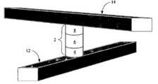
- FIG. 1is a perspective view showing a vertical polysilicon diode that may advantageously be formed having a chemically grown oxide film according to an embodiment of the invention.
- FIGS. 2 a and 2 bare cross-sectional views showing stages in formation of a vertical polysilicon diode formed having a chemically grown oxide film within the device according to a preferred embodiment of the invention.
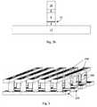
- FIG. 3is a perspective view of a memory level of memory cells like those shown in FIG. 2 b.
- FIGS. 4 a - 4 care cross-sectional views showing stages of fabrication of a first memory level of a monolithic three dimensional memory array formed according to a preferred embodiment of the present invention.
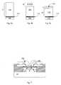
- FIGS. 5 a and 5 bare cross-sectional views of vertical diodes formed according to embodiments of the present invention.
- FIGS. 6 a - 6 care cross-sectional views illustrating loss of semiconductor thickness during formation of a diode formed according to an embodiment of the present invention.
- FIG. 7is a cross-sectional view of another embodiment of the present invention.
- FIG. 1shows a vertically oriented p-i-n diode 2 , formed of polycrystalline silicon (in this discussion, polycrystalline silicon will be referred to as polysilicon.)
- the diodeis formed between bottom conductor 12 and top conductor 14 .
- Bottom region 4is heavily doped with an n-type dopant, such as phosphorus or arsenic
- middle region 6is intrinsic polysilicon, which is not intentionally doped
- top region 8is heavily doped with a p-type dopant such as boron or BCl 3 .
- Many other semiconductor devicesincluding p-n diodes, Zener diodes, thyristors, bipolar transistors, etc., include regions having different doping characteristics.
- the p-i-n diode 2 of FIG. 1is presented as an example.
- the difference in doping characteristics between these different regionsmust be maintained for the device to function.
- Dopantscan be introduced into semiconductor material by several methods, including ion implantation or diffusion from a nearby dopant source. If the semiconductor material is deposited, it can be doped in situ, by flowing a gas that will provide the dopant during deposition, so that dopant atoms are incorporated into the semiconductor material as it is deposited.
- n-type dopantsmay diffuse, however, especially when provided with thermal energy. Additionally, most n-type dopants, such as phosphorus and arsenic, have a strong preference to be located on the surface of deposited silicon, rather than buried.
- n-type dopantssuch as phosphorus and arsenic
- SiH 4a typical precursor gas to deposit silicon
- PH 3a typical precursor gas to deposit silicon
- PH 3which will provide phosphorus.
- the flow of PH 3is stopped, while SiH 4 flow continues.
- the silicon of region 6is deposited without dopant, but phosphorus from region 4 , seeking the surface, diffuses into region 6 during deposition.
- a significant thickness of siliconmust be deposited to guarantee that a sufficient thickness of region 6 is deposited which includes no phosphorus. Unwanted dopant diffusion from heavily doped region 4 to intrinsic region 6 makes it difficult to form a sharp junction between these regions, and may force the overall height of the diode 2 to be more than desired.
- n-type dopants having strong affinity for the film surfaceare prone to unwanted diffusion. Elevated temperature processing will cause most dopants to diffuse, and boron, the most popular p-type dopant, diffuses rapidly in silicon.
- a barrier materialcould serve to impede dopant diffusion.
- a non-semiconductor material between semiconductor layershas been impractical because such a barrier would disrupt the electrical performance of the device.
- Siliconthe most commonly used semiconductor material, can be oxidized to form a high-quality oxide, silicon dioxide.
- a thermally grown silicon dioxide layerwill prevent or slow diffusion of dopants, but will also act as an unwanted dielectric barrier. As the silicon dioxide layer is made thinner, it allows more current flow, but becomes a less effective barrier to diffusion. Also, the temperatures required to perform thermal oxidation will promote unwanted diffusion elsewhere on the wafer.
- Conductive barrier materialslike titanium nitride, disrupt the electrical performance of the device.
- aspects of the present inventionprovide for semiconductor devices that include a chemically grown oxide (CGO) film that serves as a highly effective dopant diffusion barrier, even when formed so thin that it does not act as a dielectric barrier and thus can be formed between layers in an active device.
- this CGO filmis grown by immersing a layer of silicon or a silicon-rich alloy in a chemical wet bath. This is a low-temperature growth technique which will not increase the overall thermal budget. Limiting exposure to high-temperature processes reduces undesirable side effects, such as dopant diffusion elsewhere in the device, or peeling of, for example, metal or silicon dioxide layers or elements caused by differential expansion and contraction of unlike materials when heated and cooled.
- Such a CGO filmcan be formed in the vertically oriented polysilicon diode of FIG. 1 .
- the diodeis preferably formed above a conventional monocrystalline silicon wafer, though other substrates may be used.
- bottom conductor 12is formed, dielectric is deposited between adjacent conductors, and a planarization step removes overfill of dielectric,.forming a planar surface and exposing the top of conductor 12 .
- Conductor 12is shown in cross-section extending left-to-right across the page.
- the first layer 4 of silicon heavily doped with an n-type dopant, such as phosphorus,is deposited on the planarized surface.
- the waferis removed from the chamber and dipped in a conventional HF solution to remove any native oxide.
- the waferis preferably immersed in a chemical wet bath, preferably comprising H 2 O 2 and a chemical that will contribute nitrogen, for example NH 4 OH.
- a dip of about 5 minutes at about 55 degrees C., for example,will form a very thin CGO film 10 , about 4.7 angstroms thick. (The thickness of CGO film 10 is exaggerated. If it were shown to scale, CGO film 10 would not be visible.)
- the waferis returned to the chamber, and the remaining thickness of silicon 6 is deposited.
- a pattern and etch stepis performed next, forming the pillar-shaped diode 2 .
- Gaps between the diodes 2are filled with dielectric fill (not shown); a planarization step, for example by chemical mechanical polishing (CMP) removes the overfill of dielectric to expose the tops of diodes 2 .
- Top heavily doped p-type region 8is formed by ion implantation. After implantation, the top conductor 14 (shown in cross-section, extending out of the page) will be formed.
- a CGO film grown as describedincludes a small amount, for example about 0.4 atomic percent, of nitrogen.
- the amount of included nitrogenmay vary, for example from about 0.2 atomic percent to about 2 atomic percent or more. Inclusion of a small percentage of nitrogen in oxide films has been shown to impede dopant diffusion. Without wishing to be bound by any particular theory, it is believed that the incorporated nitrogen in the CGO film of the present invention gives the film its property as a superior barrier to dopant diffusion when compared with silicon dioxide films without nitrogen.
- This filmis formed extremely thin, and thus does not form a dielectric barrier that will interfere with the function of p-i-n diode 2 .
- CGO film 10heavily doped n-type region 4 is in effective electrical contact with intrinsic region 6 .
- the CGO film of the present inventioncan be formed between intrinsic region 6 and top heavily doped p-type region 8 instead or as well.
- Top heavily doped p-type region 10can be doped by ion implantation, as described, or in situ doped.
- Bottom region 4could be doped by ion implantation or some other method. The polarity of doped regions 2 and 6 could be reversed.
- diode 2is an example of a semiconductor device in an integrated circuit comprising: a first semiconductor layer; a chemically grown oxide grown on the first semiconductor layer, wherein the chemically grown oxide comprises nitrogen and is no more than about 7 angstroms thick; and a second semiconductor layer in immediate contact with the chemically grown oxide, wherein the first semiconductor layer or the second semiconductor layer is doped with a first conductivity-enhancing dopant, and wherein, after fabrication of the integrated circuit is complete, a concentration of the first conductivity-enhancing dopant is at least ten times higher in one of the first semiconductor or the second semiconductor layer than in the other of the first semiconductor layer or the second semiconductor layer.
- the difference in dopant concentration in the first and second semiconductor layerscan be much greater, for example about 100 or 1000 times.
- heavily doped layer 4can have a dopant concentration between about 1 ⁇ 10 19 and about 3 ⁇ 10 21 atoms/cm 3
- intrinsic layer 6has a dopant concentration between about 1 ⁇ 10 15 and about 1 ⁇ 10 18 atoms/cm 3 .
- elevated temperaturesfor example 500, 600, or 700 degrees C. or greater.
- Temperaturemay be elevated during various processes, for example during an anneal step performed to crystallize the semiconductor material.
- the first and second semiconductor layersare diode portions.
- one layeris heavily doped while the other is substantially undoped; in other embodiments (p-n diodes, for example) the first semiconductor layer can be doped with a dopant of a first conductivity type, while the second semiconductor layer is doped with a dopant of a second conductivity type, the second type opposite the first type.
- the CGO filmserves to prevent diffusion of dopants between the first and second semiconductor layers.
- the first and second semiconductor layersare in electrical contact.
- the '549 applicationdescribes a monolithic three dimensional memory array including vertically oriented p-i-n diodes like diode 2 of FIG. 1 .
- the polysilicon of the p-i-n diodeis in a high-resistance state.
- Application of a programming voltagepermanently changes the nature of the polysilicon, rendering it low-resistance. It is believed the change is caused by an increase in the degree of order in the polysilicon, as described more fully in Herner et al., Ser. No. 11/148,530, “Nonvolatile Memory Cell Operating by Increasing Order in Polycrystalline Semiconductor Material,” filed Jun. 8, 2005 and hereby incorporated by reference.
- This change in resistanceis stable and readily detectable, and thus can record a data state, allowing the device to operate as a memory cell.
- a first memory levelis formed above the substrate, and additional memory levels may be formed above it.
- a shorter dioderequires a lower programming voltage and decreases the aspect ratio of the gaps between adjacent diodes. Very high-aspect ratio gaps are difficult to fill without voids. A thickness of at least 600 angstroms is preferred for the intrinsic region to reduce current leakage in reverse bias of the diode. Inclusion of a CGO film in such a diode according to aspects of the present invention will allow for sharper transitions in the dopant profile, and thus reduce overall diode height.
- a monolithic three dimensional memory arrayis one in which multiple memory levels are formed above a single substrate, such as a wafer, with no intervening substrates.
- the layers forming one memory levelare deposited or grown directly over the layers of an existing level or levels.
- stacked memorieshave been constructed by forming memory levels on separate substrates and adhering the memory levels atop each other, as in Leedy, U.S. Pat. No. 5,915,167, “Three dimensional structure memory.”
- the substratesmay be thinned or removed from the memory levels before bonding, but as the memory levels are initially formed over separate substrates, such memories are not true monolithic three dimensional memory arrays.
- the problem of dopant diffusionis aggravated in fabrication of a monolithic three dimensional memory array, since devices formed in the first memory level are exposed to the thermal processing required to create the memory levels above it, which are necessarily formed after it.
- the CGO film of the present inventionis advantageously used in such an array.
- FIG. 3shows a memory level of exemplary memory cells formed according to an embodiment of the present invention, including bottom conductors 200 , pillars 300 (each pillar 300 comprising a diode), and top conductors 400 . Fabrication of such a memory level, including a CGO film formed according to embodiments of the present invention within each diode (not shown) will be described in detail. More detailed information regarding fabrication of a similar memory level is provided in the '470, '549, and '824 applications, previously incorporated. More information on fabrication of related memories is provided in Hemer et al., U.S. patent application Ser. No.
- This substrate 100can be any semiconducting substrate as known in the art, such as monocrystalline silicon, IV-IV compounds like silicon-germanium or silicon-germanium-carbon, III-V compounds, II-VII compounds, epitaxial layers over such substrates, or any other semiconducting material.
- the substratemay include integrated circuits fabricated therein.
- the insulating layer 102is formed over substrate 100 .
- the insulating layer 102can be silicon oxide, silicon nitride, high-dielectric film, Si—C—O—H film, or any other suitable insulating material.
- the first conductors 200are formed over the substrate and insulator.
- An adhesion layer 104may be included between the insulating layer 102 and the conducting layer 106 to help the conducting layer 106 adhere. If the overlying conducting layer is tungsten, titanium nitride is preferred as adhesion layer 104 .
- Conducting layer 106can comprise any conducting material known in the art, such as tungsten, or other materials, including tantalum, titanium, copper, cobalt, or alloys thereof.
- the layerswill be patterned and etched using any suitable masking and etching process to form substantially parallel, substantially coplanar conductors 200 , shown in FIG. 4 a in cross-section.
- photoresistis deposited, patterned by photolithography and the layers etched, and then the photoresist removed using standard process techniques.
- Conductors 200could be formed by a Damascene method instead.
- Dielectric material 108is deposited over and between conductor rails 200 .
- Dielectric material 108can be any known electrically insulating material, such as silicon oxide, silicon nitride, or silicon oxynitride. In a preferred embodiment, silicon doxide is used as dielectric material 108 .
- FIG. 4 aThis removal of dielectric overfill to form planar surface 109 can be performed by any process known in the art, such as chemical mechanical planarization (CMP) or etchback.
- CMPchemical mechanical planarization
- An etchback technique that may advantageously be usedis described in Raghuram et al., U.S. application Ser. No. 10/883417, “Nonselective Unpatterned Etchback to Expose Buried Patterned Features,” filed Jun. 30, 2004 and hereby incorporated by reference.
- a plurality of substantially parallel first conductorshave been formed at a first height above substrate 100 .
- a barrier layer 110is deposited as the first layer after planarization of the conductor rails.
- Any suitable materialcan be used in the barrier layer, including tungsten nitride, tantalum nitride, titanium nitride, or combinations of these materials.
- titanium nitrideis used as the barrier layer.
- the barrier layeris titanium nitride, it can be deposited in the same manner as the adhesion layer described earlier.
- the semiconductor materialcan be silicon, germanium, a silicon-germanium alloy, or other suitable semiconductors or compounds.
- silicongermanium
- a silicon-germanium alloyor other suitable semiconductors or compounds.
- this descriptionwill refer to the semiconductor material as silicon, but it will be understood that the skilled practitioner may select any of these other suitable materials instead.
- the pillarcomprises a semiconductor junction diode.
- a preferred junction diodehas a bottom heavily doped region 112 , intrinsic region 114 , and top heavily doped region 116 .
- the conductivity type of bottom region 112 and top region 116are opposite: Either region 112 is p-type while region 116 is n-type, or region 112 is n-type while region 116 is p-type.
- Middle region 114is intrinsic, or not intentionally doped, though in some embodiments it may be lightly doped. An undoped region will never be perfectly electrically neutral, and will always have defects or contaminants that cause it to behave as if slightly n-doped or p-doped.
- bottom region 112will be n-type while top region 116 is p-type. It will be understood that these conductivity types could be reversed, as in FIG. 5 b.
- a CGO film 113is interposed between regions 112 and 114 .
- bottom heavily doped region 112can be formed by any deposition and doping method known in the art.
- the siliconcan be deposited and then doped, but is preferably doped in situ by flowing a donor gas providing n-type dopant atoms, for example phosphorus, during deposition of the silicon.
- Heavily doped region 112is preferably between about 100 and about 800 angstroms thick, preferably about 200 angstroms thick.
- Layer 112is preferably at least 80 atomic percent silicon. It is preferred that layer 112 be high in silicon, so that the CGO film to be formed is predominantly silicon dioxide, rather than germanium oxide.
- the wafersare removed from the chamber.
- An HF dipmay be performed to remove any native oxide that has formed on the silicon.
- the siliconis then exposed to a solution containing H 2 O 2 and a component that will provide nitrogen.
- the wafermay be immersed in a bath containing NH 4 OH, H 2 O 2 , and H 2 O, in equal amounts, for at least one minute, for example for about five minutes or longer.
- the bathis preferably heated to a temperature between about 25 and about 180 degrees C., for example about 55 degrees C. This step will cause growth of thin CGO film 113 .
- This layerwill be very thin, preferably less than about 10 angstroms thick, preferably between about 4 and about 7 angstroms thick, for example about 4.7 angstroms thick, and may or may not be continuous.
- CGO film 113is necessarily depicted with its thickness exaggerated relative to the other layers.
- Undoped siliconis to be deposited next to form intrinsic layer 114 . It will be recalled that the previous deposition was of heavily doped n-type silicon to form layer 112 . During this deposition, heavily doped silicon was deposited not only on the wafers, but on chamber walls and other surfaces. During deposition of intrinsic silicon layer 114 , doped silicon on chamber surfaces from the previous deposition may provide unwanted dopant to the intrinsic silicon; such unintentional doping is called autodoping. To avoid autodoping, either the chamber can be cleaned before the deposition of intrinsic layer 114 or a thin undoped layer can be deposited in an empty chamber, effectively sealing in the earlier-deposited dopants. The method of depositing a passivation layer to prevent autodoping is described in Herner et al., U.S. Pat. No. 6,635,556, “Method of Preventing Autodoping,” hereby incorporated by reference.
- intrinsic layer 114is deposited on CGO film 113 .
- Intrinsic layer 114can be formed by any method known in the art.
- Layer 114can be silicon, germanium, or any alloy of silicon or germanium.
- heavily doped p-type layer 116will be formed by ion implantation.
- FIG. 6 aintrinsic layer 114 has a deposited thickness A.
- an upcoming planarization stepwill remove a thickness B, and, in FIG. 6 c, ion implantation to form region 116 will cause a thickness C to be heavily doped.
- intrinsic layer 114should have thickness D.
- the thickness A to be depositedis the sum of the ultimate desired thickness D of the intrinsic region 114 , the thickness C of heavily doped p-type region 116 to be formed by implantation, and thickness B to be lost during planarization.
- intrinsic region 114is preferably between about 600 and about 2000 angstroms, for example about 1600 angstroms.
- Heavily doped p-type layer 116is between about 100 and about 1000 angstroms, preferably about 200 angstroms. The amount lost during planarization will most likely be between about 400 and about 800 angstroms, depending on the planarization method used.
- the thickness to be deposited undoped in this stepis between about 1100 and about 3800 angstrom, preferably about 2600 angstroms.
- Pillars 300should have about the same pitch and about the same width as conductors 200 below, such that each pillar 300 is formed on top of a conductor 200 . Some misalignment can be tolerated.
- the pillars 300can be formed using any suitable masking and etching process.
- photoresistcan be deposited, patterned using standard photolithography techniques, and etched, then the photoresist removed.
- a hard mask of some other materialfor example silicon dioxide, can be formed on top of the semiconductor layer stack, with bottom antireflective coating (BARC) on top, then patterned and etched.
- BARCbottom antireflective coating
- DARCdielectric antireflective coating
- Dielectric material 108is deposited over and between the semiconductor pillars 300 , filling the gaps between them.
- Dielectric material 108can be any known electrically insulating material, such as silicon oxide, silicon nitride, or silicon oxynitride. In a preferred embodiment, silicon dioxide is used as the insulating material.
- the dielectric material on top of the pillars 300is removed, exposing the tops of pillars 300 separated by dielectric material 108 , and leaving a substantially planar surface.
- This removal of dielectric overfillcan be performed by any process known in the art, such as CMP or etchback.
- CMP or etchbackion implantation is performed, forming heavily doped p-type top region 116 .
- the p-type dopantis preferably boron or BCL 3 .
- the resulting structureis shown in FIG. 4 b.
- the resistivity of the semiconductor material of the diodedetectably and permanently changes when subjected to a programming voltage.
- a dielectric rupture antifusewhich is intact before programming and is ruptured during programming, may be included in the cell to increase the difference between current flow observed when a read voltage is applied to a programmed vs. an unprogrammed cell.
- dielectric rupture antifuse 118can be formed by any appropriate method, including thermal oxidation of a portion of heavily doped p-type region 116 .
- Silicon dioxideis a high-quality oxide
- germanium oxideis a very poor quality oxide, and is water-soluble. So long as the semiconductor material at the top of heavily doped p-type layer 116 is at least about 80 atomic percent silicon, this oxide can be thermally grown, as shown in FIG. 4 c, and will be predominantly high-quality silicon dioxide.
- this layercan be deposited instead, and may be any appropriate dielectric material. For example, a layer of Al 2 O 3 can be deposited at about 150 degrees C. Other materials may be used.
- Dielectric rupture antifuse 118is preferably between about 20 and about 80 angstroms thick, preferably about 50 angstroms thick. In other embodiments, dielectric rupture antifuse 118 may be omitted.
- Top conductors 400can be formed in the same manner as bottom conductors 200 , for example by depositing adhesion layer 120 , preferably of titanium nitride, and conductive layer 122 , preferably of tungsten. Conductive layer 122 and adhesion layer 120 are then patterned and etched using any suitable masking and etching technique to form substantially parallel, substantially coplanar conductors 400 , shown in FIG. 4 c extending left-to-right across the page. In a preferred embodiment, photoresist is deposited, patterned by photolithography and the layers etched, and then the photoresist removed using standard process techniques.
- the dielectric materialcan be any known electrically insulating material, such as silicon oxide, silicon nitride, or silicon oxynitride. In a preferred embodiment, silicon oxide is used as this dielectric material.
- CGO film 113does not behave as a dielectric rupture antifuse. With applied voltage, a dielectric rupture antifuse initially prevents current flow, building up capacitance. When capacitance becomes too high, the dielectric rupture antifuse suffers dielectric breakdown, and a permanent conductive path is formed through the antifuse. CGO film 113 does not form a dielectric barrier; it is too thin and too conductive to build up sufficient capacitance to cause dielectric breakdown.
- Formation of a first memory levelhas been described. Additional memory levels can be formed above this first memory level.
- conductorscan be shared between memory levels; i.e. top conductor 400 would serve as the bottom conductor of the next memory level.
- an interlevel dielectric(not shown) is formed above the first memory level of FIG. 4 c, its surface planarized, and construction of a second memory level begins on this planarized interlevel dielectric, with no shared conductors.
- a monolithic three dimensional memory array formed above a substratecomprises at least a first memory level formed at a first height above the substrate and a second memory level formed at a second height different from the first height. Three, four, eight, or indeed any number of memory levels can be formed above the substrate in such a multilevel array.
- the detailed example givendescribed a method for forming a semiconductor device, the method comprising: forming a first semiconductor layer; growing a chemically grown oxide on the first semiconductor layer in a liquid ambient; forming a second semiconductor layer directly on the-chemically grown oxide, wherein the first semiconductor layer or the second semiconductor layer is doped with a first conductivity-enhancing dopant.
- the first semiconductor layer, the chemically grown oxide layer, and the second semiconductor layermay be subjected to a temperature exceeding about 700 degrees C.
- the chemically grown oxideinhibits diffusion of the first conductivity-enhancing dopant between the first and second semiconductor layers.
- a currentwill be passed between the first and second semiconductor layers.
- a nonvolatile memory cellis formed by a method comprising: depositing a first semiconductor layer above a substrate; growing a chemically grown oxide on the first semiconductor layer in a liquid ambient; depositing a second semiconductor layer above the chemically grown oxide; and forming a vertically oriented diode comprising the first semiconductor layer, the chemically grown oxide, and the second semiconductor layer, wherein the nonvolatile memory cell comprises the vertically oriented diode.
- the step of growing the chemically grown oxidecomprises immersing the first semiconductor layer in a solution comprising H 2 O 2 and a component comprising nitrogen, for example NH 4 OH. During the growing step the temperature does not exceed about 180 degrees C.
- the memory cell describedincludes a first conductor extending in a first direction and a second conductor extending in a second direction, the second direction different from the first direction, the diode above the first conductor, the second conductor above the diode, and the vertically oriented diode disposed between the first conductor and the second conductor.
- Embodiments of the memory cellmay further include a resistance-switching element in series with the diode, such as an antifuse.
- other materials, such as nickel oxidemay be used as the resistance-switching material, as in the '939 application. If the resistance-switching element is an antifuse, the cell will be a one-time-programmable memory cell. If the resistance change is reversible, the cell may be a rewriteable memory cell.
- a bipolar transistorincludes a heavily doped emitter 202 doped with a first conductivity type dopant, typically formed in polysilicon, adjacent to base region 204 doped with a second conductivity type dopant opposite the first type.
- emitter 202is n-type while base region 204 is p-type.
- Polarities of other regionsare as indicated.
- Cross-hatched sectionsare a dielectric material, for example silicon dioxide.
- Base region 204may be formed either in a monocrystalline wafer substrate or in polysilicon.
- Dopantmay diffuse from emitter 202 to base region 204 , which will compromise device performance by shorting the device or causing higher leakage in the “off” state, but emitter 202 and base region 204 must be in electrical contact.
- Bipolar transistorsare well known in the art; thus this device will not be described in detail.
- a CGO film 206 formed according to the present inventionwill prevent unwanted dopant diffusion from emitter 202 to base region 204 without preventing the electrical contact required for device function.
- a CGO film 206is formed as described earlier, by exposing base region 204 to a solution comprising H 2 O 2 and a component that will provide nitrogen, before depositing emitter 202 .
- a CGO filmcan also act as a dopant diffusion barrier in a CMOS transistor.
- the CGO filmcan be formed with sufficient thickness to provide a dielectric barrier, or can be coupled with another film that will provide a dielectric barrier, and can act as a gate oxide or part of a gate oxide, preventing dopant diffusion from a heavily doped gate to an undoped or lightly doped channel region.
Landscapes
- Engineering & Computer Science (AREA)
- Computer Hardware Design (AREA)
- Semiconductor Memories (AREA)
Abstract
Description
- This application is a continuation-in-part of Herner et al., U.S. patent application Ser. No. 11/015,824, “Nonvolatile Memory Cell Comprising a Reduced Height Vertical Diode,” filed Dec. 17, 2004 and hereinafter the '824 application, which is a continuation-in-part of Herner, U.S. patent application Ser. No. 10/955,549, “Nonvolatile Memory Cell Without a Dielectric Antifuse Having High- and Low-Impedance States,” filed Sep. 29, 2004, hereinafter the '549 application; which is a continuation-in-part of Herner et al., U.S. patent application Ser. No. 10/855784, “A High-Density Three-Dimensional Memory Cell,” filed May 26, 2004; which is a continuation of Herner et al., U.S. patent application Ser. No. 10/326470, “An Improved Method for Making High-Density Nonvolatile Memory,” filed Dec. 19, 2002 (since abandoned) and hereinafter the '470 application, all assigned to the assignee of the present invention and hereby incorporated by reference in their entirety.
- The invention relates to an ultrathin chemically grown oxide layer which serves to prevent dopant diffusion between semiconductor layers.
- P-type and n-type dopants are added to semiconductor material, notably silicon, to enhance conductivity. Most semiconductor devices require adjacent regions of the device to have different dopant characteristics: One region is to be heavily doped while an adjacent region is undoped or lightly doped, for example; or a heavily doped p-type region may be adjacent to a heavily doped n-type region.
- Dopants do not reliably remain where they've been placed through implantation or in situ doping, however. Dopants tend to diffuse, and, particularly in smaller devices, sharp transitions in doping profiles can be difficult to maintain.
- Barriers can be used to prevent dopant diffusion, but in general such barriers will significantly change the electrical properties of the device. A thick oxide layer, for example, would form an unwanted dielectric barrier.
- There is a need, therefore, for a method to prevent or inhibit dopant diffusion between semiconductor regions in a semiconductor device without disrupting the electrical function of the device.
- The present invention is defined by the following claims, and nothing in this section should be taken as a limitation on those claims. In general, the invention is directed to a chemically grown oxide film that serves as a dopant diffusion barrier.
- A first aspect of the invention provides for a semiconductor device in an integrated circuit comprising: a first semiconductor layer; a chemically grown oxide grown on the first semiconductor layer, wherein the chemically grown oxide comprises nitrogen and is no more than about 7 angstroms thick; and a second semiconductor layer in immediate contact with the chemically grown oxide, wherein the first semiconductor layer or the second semiconductor layer is doped with a first conductivity-enhancing dopant, and wherein, after fabrication of the integrated circuit is complete, a concentration of the first conductivity-enhancing dopant is at least ten times higher in one of the first semiconductor or the second semiconductor layer than in the other of the first semiconductor layer or the second semiconductor layer.
- Another aspect of the invention provides for a method for forming a semiconductor device, the method comprising: forming a first semiconductor layer; growing a chemically grown oxide on the first semiconductor layer in a liquid ambient; forming a second semiconductor layer directly on the chemically grown oxide, wherein the first semiconductor layer or the second semiconductor layer is doped with a first conductivity-enhancing dopant; and subjecting the first semiconductor layer, the chemically grown oxide layer, and the second semiconductor layer to a temperature exceeding about 700 degrees C., wherein the chemically grown oxide inhibits diffusion of the first conductivity-enhancing dopant between the first and second semiconductor layers.
- A preferred embodiment of the invention provides for a method for forming a nonvolatile memory cell, the method comprising: depositing a first semiconductor layer above a substrate; growing a chemically grown oxide on the first semiconductor layer in a liquid ambient; depositing a second semiconductor layer above the chemically grown oxide; and forming a vertically oriented diode comprising the first semiconductor layer, the chemically grown oxide, and the second semiconductor layer, wherein the nonvolatile memory cell comprises the vertically oriented diode.
- Another preferred embodiment of the invention provides for a method to form a monolithic three dimensional memory array, the method comprising: i) forming a first memory level above a substrate, the first memory level formed by a method comprising: a) forming a first plurality of substantially parallel conductors extending in a first direction; b) depositing a first semiconductor layer above the first conductors; c) growing a first chemically grown oxide on the first semiconductor layer in a liquid ambient; d) depositing a second semiconductor layer above the first chemically grown oxide; f) patterning and etching the first semiconductor layer and the second semiconductor layer to form a first plurality of pillars; and e) forming a second plurality of substantially parallel conductors above the first pillars, the second conductors extending in a second direction different from the first direction, each of the first pillars disposed between one of the first conductors and one of the second conductors; and ii) monolithically forming a second memory level above the first memory level.
- Each of the aspects and embodiments of the invention described herein can be used alone or in combination with one another.
- The preferred aspects and embodiments will now be described with reference to the attached drawings.
FIG. 1 is a perspective view showing a vertical polysilicon diode that may advantageously be formed having a chemically grown oxide film according to an embodiment of the invention.FIGS. 2 aand2bare cross-sectional views showing stages in formation of a vertical polysilicon diode formed having a chemically grown oxide film within the device according to a preferred embodiment of the invention.FIG. 3 is a perspective view of a memory level of memory cells like those shown inFIG. 2 b.FIGS. 4 a-4care cross-sectional views showing stages of fabrication of a first memory level of a monolithic three dimensional memory array formed according to a preferred embodiment of the present invention.FIGS. 5 aand5bare cross-sectional views of vertical diodes formed according to embodiments of the present invention.FIGS. 6 a-6care cross-sectional views illustrating loss of semiconductor thickness during formation of a diode formed according to an embodiment of the present invention.FIG. 7 is a cross-sectional view of another embodiment of the present invention.- Semiconductor devices are doped with p-type and n-type dopants to enhance conductivity. Most semiconductor devices require sharp transitions in dopant profiles. For example,
FIG. 1 shows a vertically orientedp-i-n diode 2, formed of polycrystalline silicon (in this discussion, polycrystalline silicon will be referred to as polysilicon.) The diode is formed betweenbottom conductor 12 andtop conductor 14.Bottom region 4 is heavily doped with an n-type dopant, such as phosphorus or arsenic,middle region 6 is intrinsic polysilicon, which is not intentionally doped, andtop region 8 is heavily doped with a p-type dopant such as boron or BCl3. (Many other semiconductor devices, including p-n diodes, Zener diodes, thyristors, bipolar transistors, etc., include regions having different doping characteristics. Thep-i-n diode 2 ofFIG. 1 is presented as an example.) The difference in doping characteristics between these different regions must be maintained for the device to function. - Dopants can be introduced into semiconductor material by several methods, including ion implantation or diffusion from a nearby dopant source. If the semiconductor material is deposited, it can be doped in situ, by flowing a gas that will provide the dopant during deposition, so that dopant atoms are incorporated into the semiconductor material as it is deposited.
- Dopants may diffuse, however, especially when provided with thermal energy. Additionally, most n-type dopants, such as phosphorus and arsenic, have a strong preference to be located on the surface of deposited silicon, rather than buried. Referring to
FIG. 1 , heavily doped n-type region 4 can be formed by flowing SiH4, a typical precursor gas to deposit silicon, along with PH3, which will provide phosphorus. To formintrinsic region 6, the flow of PH3is stopped, while SiH4flow continues. The silicon ofregion 6 is deposited without dopant, but phosphorus fromregion 4, seeking the surface, diffuses intoregion 6 during deposition. A significant thickness of silicon must be deposited to guarantee that a sufficient thickness ofregion 6 is deposited which includes no phosphorus. Unwanted dopant diffusion from heavily dopedregion 4 tointrinsic region 6 makes it difficult to form a sharp junction between these regions, and may force the overall height of thediode 2 to be more than desired. - Not only n-type dopants having strong affinity for the film surface are prone to unwanted diffusion. Elevated temperature processing will cause most dopants to diffuse, and boron, the most popular p-type dopant, diffuses rapidly in silicon.
- Inclusion of a barrier material could serve to impede dopant diffusion. In general, though, a non-semiconductor material between semiconductor layers has been impractical because such a barrier would disrupt the electrical performance of the device. Silicon, the most commonly used semiconductor material, can be oxidized to form a high-quality oxide, silicon dioxide. A thermally grown silicon dioxide layer will prevent or slow diffusion of dopants, but will also act as an unwanted dielectric barrier. As the silicon dioxide layer is made thinner, it allows more current flow, but becomes a less effective barrier to diffusion. Also, the temperatures required to perform thermal oxidation will promote unwanted diffusion elsewhere on the wafer. Conductive barrier materials, like titanium nitride, disrupt the electrical performance of the device.
- Aspects of the present invention provide for semiconductor devices that include a chemically grown oxide (CGO) film that serves as a highly effective dopant diffusion barrier, even when formed so thin that it does not act as a dielectric barrier and thus can be formed between layers in an active device. In preferred embodiments this CGO film is grown by immersing a layer of silicon or a silicon-rich alloy in a chemical wet bath. This is a low-temperature growth technique which will not increase the overall thermal budget. Limiting exposure to high-temperature processes reduces undesirable side effects, such as dopant diffusion elsewhere in the device, or peeling of, for example, metal or silicon dioxide layers or elements caused by differential expansion and contraction of unlike materials when heated and cooled.
- Such a CGO film can be formed in the vertically oriented polysilicon diode of
FIG. 1 . The diode is preferably formed above a conventional monocrystalline silicon wafer, though other substrates may be used. Turning toFIG. 2 a,bottom conductor 12 is formed, dielectric is deposited between adjacent conductors, and a planarization step removes overfill of dielectric,.forming a planar surface and exposing the top ofconductor 12.Conductor 12 is shown in cross-section extending left-to-right across the page. Thefirst layer 4 of silicon heavily doped with an n-type dopant, such as phosphorus, is deposited on the planarized surface. After deposition oflayer 4, the wafer is removed from the chamber and dipped in a conventional HF solution to remove any native oxide. Next the wafer is preferably immersed in a chemical wet bath, preferably comprising H2O2and a chemical that will contribute nitrogen, for example NH4OH. A dip of about 5 minutes at about 55 degrees C., for example, will form a verythin CGO film 10, about 4.7 angstroms thick. (The thickness ofCGO film 10 is exaggerated. If it were shown to scale,CGO film 10 would not be visible.) Next the wafer is returned to the chamber, and the remaining thickness ofsilicon 6 is deposited. - Turning to
FIG. 2 b,a pattern and etch step is performed next, forming the pillar-shapeddiode 2. As will be appreciated by those skilled in the art, it is usual to form a large number of such pillars in a single patterning step. Gaps between thediodes 2 are filled with dielectric fill (not shown); a planarization step, for example by chemical mechanical polishing (CMP) removes the overfill of dielectric to expose the tops ofdiodes 2. Top heavily doped p-type region 8 is formed by ion implantation. After implantation, the top conductor14 (shown in cross-section, extending out of the page) will be formed. - It has been found that very
thin CGO film 10 will prevent or inhibit diffusion of phosphorus from heavily doped n-type region 4 intointrinsic region 6. A CGO film grown as described includes a small amount, for example about 0.4 atomic percent, of nitrogen. The amount of included nitrogen may vary, for example from about 0.2 atomic percent to about 2 atomic percent or more. Inclusion of a small percentage of nitrogen in oxide films has been shown to impede dopant diffusion. Without wishing to be bound by any particular theory, it is believed that the incorporated nitrogen in the CGO film of the present invention gives the film its property as a superior barrier to dopant diffusion when compared with silicon dioxide films without nitrogen. - This film is formed extremely thin, and thus does not form a dielectric barrier that will interfere with the function of
p-i-n diode 2. Despite the presence ofCGO film 10, heavily doped n-type region 4 is in effective electrical contact withintrinsic region 6. - Many variations can be imagined. The CGO film of the present invention can be formed between
intrinsic region 6 and top heavily doped p-type region 8 instead or as well. Top heavily doped p-type region 10 can be doped by ion implantation, as described, or in situ doped.Bottom region 4 could be doped by ion implantation or some other method. The polarity ofdoped regions - To summarize,
diode 2 is an example of a semiconductor device in an integrated circuit comprising: a first semiconductor layer; a chemically grown oxide grown on the first semiconductor layer, wherein the chemically grown oxide comprises nitrogen and is no more than about 7 angstroms thick; and a second semiconductor layer in immediate contact with the chemically grown oxide, wherein the first semiconductor layer or the second semiconductor layer is doped with a first conductivity-enhancing dopant, and wherein, after fabrication of the integrated circuit is complete, a concentration of the first conductivity-enhancing dopant is at least ten times higher in one of the first semiconductor or the second semiconductor layer than in the other of the first semiconductor layer or the second semiconductor layer. The difference in dopant concentration in the first and second semiconductor layers can be much greater, for example about 100 or 1000 times. - For example, adjacent to
CGO film 10, heavily dopedlayer 4 can have a dopant concentration between about 1×10¹⁹and about 3×10²¹atoms/cm3, while adjacent to heavily dopedCGO film 10,intrinsic layer 6 has a dopant concentration between about 1×10¹⁵and about 1×10¹⁸atoms/cm3. These differences in dopant concentration are maintained even after exposure to elevated temperatures, for example 500, 600, or 700 degrees C. or greater. Temperature may be elevated during various processes, for example during an anneal step performed to crystallize the semiconductor material. - In the example given, the first and second semiconductor layers are diode portions. In this embodiment, one layer is heavily doped while the other is substantially undoped; in other embodiments (p-n diodes, for example) the first semiconductor layer can be doped with a dopant of a first conductivity type, while the second semiconductor layer is doped with a dopant of a second conductivity type, the second type opposite the first type. In any case, the CGO film serves to prevent diffusion of dopants between the first and second semiconductor layers. The first and second semiconductor layers are in electrical contact.
- The '549 application describes a monolithic three dimensional memory array including vertically oriented p-i-n diodes like
diode 2 ofFIG. 1 . As formed, the polysilicon of the p-i-n diode is in a high-resistance state. Application of a programming voltage permanently changes the nature of the polysilicon, rendering it low-resistance. It is believed the change is caused by an increase in the degree of order in the polysilicon, as described more fully in Herner et al., Ser. No. 11/148,530, “Nonvolatile Memory Cell Operating by Increasing Order in Polycrystalline Semiconductor Material,” filed Jun. 8, 2005 and hereby incorporated by reference. This change in resistance is stable and readily detectable, and thus can record a data state, allowing the device to operate as a memory cell. A first memory level is formed above the substrate, and additional memory levels may be formed above it. - As described in the '824 application, it may be advantageous to reduce the height of the p-i-n diode. A shorter diode requires a lower programming voltage and decreases the aspect ratio of the gaps between adjacent diodes. Very high-aspect ratio gaps are difficult to fill without voids. A thickness of at least 600 angstroms is preferred for the intrinsic region to reduce current leakage in reverse bias of the diode. Inclusion of a CGO film in such a diode according to aspects of the present invention will allow for sharper transitions in the dopant profile, and thus reduce overall diode height.
- This technique is particularly useful in a monolithic three dimensional memory array. A monolithic three dimensional memory array is one in which multiple memory levels are formed above a single substrate, such as a wafer, with no intervening substrates. The layers forming one memory level are deposited or grown directly over the layers of an existing level or levels. In contrast, stacked memories have been constructed by forming memory levels on separate substrates and adhering the memory levels atop each other, as in Leedy, U.S. Pat. No. 5,915,167, “Three dimensional structure memory.” The substrates may be thinned or removed from the memory levels before bonding, but as the memory levels are initially formed over separate substrates, such memories are not true monolithic three dimensional memory arrays.
- The problem of dopant diffusion is aggravated in fabrication of a monolithic three dimensional memory array, since devices formed in the first memory level are exposed to the thermal processing required to create the memory levels above it, which are necessarily formed after it. Thus the CGO film of the present invention is advantageously used in such an array.
FIG. 3 shows a memory level of exemplary memory cells formed according to an embodiment of the present invention, includingbottom conductors 200, pillars300 (eachpillar 300 comprising a diode), andtop conductors 400. Fabrication of such a memory level, including a CGO film formed according to embodiments of the present invention within each diode (not shown) will be described in detail. More detailed information regarding fabrication of a similar memory level is provided in the '470, '549, and '824 applications, previously incorporated. More information on fabrication of related memories is provided in Hemer et al., U.S. patent application Ser. No. 11/125,606, “High-Density Nonvolatile Memory Array Fabricated at Low Temperature Comprising Semiconductor Diodes,” filed May 9, 2005; Herner et al., U.S. patent application Ser. No. 10/954,577, “Junction Diode Comprising Varying Semiconductor Compositions,” filed Sep. 29, 2004; and Herner et al., U.S. patent application Ser. No. 11/125939, “Rewriteable Memory Cell Comprising a Diode and a Resistance-Switching Material,” filed May 9, 2005 and hereinafter the '939 application, all owned by the assignee of the present invention and hereby incorporated by reference. To avoid obscuring the invention, not all of this detail will be included in this description, but no teaching of these or other incorporated patents and applications is intended to be excluded. It will be understood that this example is non-limiting, and that these details can be modified, omitted, or augmented while the results fall within the scope of the invention.- Fabrication
- Fabrication of a single memory level will be described in detail. Additional memory levels can be stacked, each monolithically formed above the one below it.
- Turning to
FIG. 4 a,formation of the memory begins with asubstrate 100. Thissubstrate 100 can be any semiconducting substrate as known in the art, such as monocrystalline silicon, IV-IV compounds like silicon-germanium or silicon-germanium-carbon, III-V compounds, II-VII compounds, epitaxial layers over such substrates, or any other semiconducting material. The substrate may include integrated circuits fabricated therein. - An insulating
layer 102 is formed oversubstrate 100. The insulatinglayer 102 can be silicon oxide, silicon nitride, high-dielectric film, Si—C—O—H film, or any other suitable insulating material. - The
first conductors 200 are formed over the substrate and insulator. Anadhesion layer 104 may be included between the insulatinglayer 102 and theconducting layer 106 to help theconducting layer 106 adhere. If the overlying conducting layer is tungsten, titanium nitride is preferred asadhesion layer 104. - The next layer to be deposited is conducting
layer 106. Conductinglayer 106 can comprise any conducting material known in the art, such as tungsten, or other materials, including tantalum, titanium, copper, cobalt, or alloys thereof. - Once all the layers that will form the conductor rails have been deposited, the layers will be patterned and etched using any suitable masking and etching process to form substantially parallel, substantially
coplanar conductors 200, shown inFIG. 4 ain cross-section. In one embodiment, photoresist is deposited, patterned by photolithography and the layers etched, and then the photoresist removed using standard process techniques.Conductors 200 could be formed by a Damascene method instead. - Next a
dielectric material 108 is deposited over and between conductor rails200.Dielectric material 108 can be any known electrically insulating material, such as silicon oxide, silicon nitride, or silicon oxynitride. In a preferred embodiment, silicon doxide is used asdielectric material 108. - Finally, excess
dielectric material 108 on top ofconductor rails 200 is removed, exposing the tops ofconductor rails 200 separated bydielectric material 108, and leaving a substantiallyplanar surface 109. The resulting structure is shown inFIG. 4 a.This removal of dielectric overfill to formplanar surface 109 can be performed by any process known in the art, such as chemical mechanical planarization (CMP) or etchback. An etchback technique that may advantageously be used is described in Raghuram et al., U.S. application Ser. No. 10/883417, “Nonselective Unpatterned Etchback to Expose Buried Patterned Features,” filed Jun. 30, 2004 and hereby incorporated by reference. At this stage, a plurality of substantially parallel first conductors have been formed at a first height abovesubstrate 100. - Next, turning to
FIG. 4 b,vertical pillars will be formed above completed conductor rails200. (To savespace substrate 100 is not shown inFIG. 4 b;its presence will be assumed.) Preferably abarrier layer 110 is deposited as the first layer after planarization of the conductor rails. Any suitable material can be used in the barrier layer, including tungsten nitride, tantalum nitride, titanium nitride, or combinations of these materials. In a preferred embodiment, titanium nitride is used as the barrier layer. Where the barrier layer is titanium nitride, it can be deposited in the same manner as the adhesion layer described earlier. - Next semiconductor material that will be patterned into pillars is deposited. The semiconductor material can be silicon, germanium, a silicon-germanium alloy, or other suitable semiconductors or compounds. For simplicity, this description will refer to the semiconductor material as silicon, but it will be understood that the skilled practitioner may select any of these other suitable materials instead.
- In preferred embodiments, the pillar comprises a semiconductor junction diode. Turning to
FIG. 5 a,a preferred junction diode has a bottom heavily dopedregion 112,intrinsic region 114, and top heavily dopedregion 116. The conductivity type ofbottom region 112 andtop region 116 are opposite: Eitherregion 112 is p-type whileregion 116 is n-type, orregion 112 is n-type whileregion 116 is p-type.Middle region 114 is intrinsic, or not intentionally doped, though in some embodiments it may be lightly doped. An undoped region will never be perfectly electrically neutral, and will always have defects or contaminants that cause it to behave as if slightly n-doped or p-doped. - In
FIG. 5 a,and in the exemplary array,bottom region 112 will be n-type whiletop region 116 is p-type. It will be understood that these conductivity types could be reversed, as inFIG. 5 b.ACGO film 113 is interposed betweenregions - To form the diode of
FIG. 5 a,returning toFIG. 4 b,bottom heavily dopedregion 112 can be formed by any deposition and doping method known in the art. The silicon can be deposited and then doped, but is preferably doped in situ by flowing a donor gas providing n-type dopant atoms, for example phosphorus, during deposition of the silicon. Heavily dopedregion 112 is preferably between about 100 and about 800 angstroms thick, preferably about 200 angstroms thick.Layer 112 is preferably at least 80 atomic percent silicon. It is preferred thatlayer 112 be high in silicon, so that the CGO film to be formed is predominantly silicon dioxide, rather than germanium oxide. - Next the wafers are removed from the chamber. An HF dip may be performed to remove any native oxide that has formed on the silicon. The silicon is then exposed to a solution containing H2O2and a component that will provide nitrogen. For example, the wafer may be immersed in a bath containing NH4OH, H2O2, and H2O, in equal amounts, for at least one minute, for example for about five minutes or longer. The bath is preferably heated to a temperature between about 25 and about 180 degrees C., for example about 55 degrees C. This step will cause growth of
thin CGO film 113. This layer will be very thin, preferably less than about 10 angstroms thick, preferably between about 4 and about 7 angstroms thick, for example about 4.7 angstroms thick, and may or may not be continuous. In order to be shown inFIG. 4 b,CGO film 113 is necessarily depicted with its thickness exaggerated relative to the other layers. - Undoped silicon is to be deposited next to form
intrinsic layer 114. It will be recalled that the previous deposition was of heavily doped n-type silicon to formlayer 112. During this deposition, heavily doped silicon was deposited not only on the wafers, but on chamber walls and other surfaces. During deposition ofintrinsic silicon layer 114, doped silicon on chamber surfaces from the previous deposition may provide unwanted dopant to the intrinsic silicon; such unintentional doping is called autodoping. To avoid autodoping, either the chamber can be cleaned before the deposition ofintrinsic layer 114 or a thin undoped layer can be deposited in an empty chamber, effectively sealing in the earlier-deposited dopants. The method of depositing a passivation layer to prevent autodoping is described in Herner et al., U.S. Pat. No. 6,635,556, “Method of Preventing Autodoping,” hereby incorporated by reference. - When the wafer is returned to the chamber,
intrinsic layer 114 is deposited onCGO film 113.Intrinsic layer 114 can be formed by any method known in the art.Layer 114 can be silicon, germanium, or any alloy of silicon or germanium. In a preferred embodiment heavily doped p-type layer 116 will be formed by ion implantation. Turning toFIG. 6 a,intrinsic layer 114 has a deposited thickness A. As shown inFIG. 6 b,an upcoming planarization step will remove a thickness B, and, inFIG. 6 c,ion implantation to formregion 116 will cause a thickness C to be heavily doped. In the finished deviceintrinsic layer 114 should have thickness D. Thus the thickness A to be deposited is the sum of the ultimate desired thickness D of theintrinsic region 114, the thickness C of heavily doped p-type region 116 to be formed by implantation, and thickness B to be lost during planarization. In the finished device,intrinsic region 114 is preferably between about 600 and about 2000 angstroms, for example about 1600 angstroms. Heavily doped p-type layer 116 is between about 100 and about 1000 angstroms, preferably about 200 angstroms. The amount lost during planarization will most likely be between about 400 and about 800 angstroms, depending on the planarization method used. The thickness to be deposited undoped in this step, then, is between about 1100 and about 3800 angstrom, preferably about 2600 angstroms. - Note that despite the presence of
CGO film 113,silicon layer 112 andsemiconductor layer 114 are in electrical contact. - Returning to
FIG. 4 b,semiconductor layers114 and112 just deposited, along withunderlying barrier layer 110, will be patterned and etched to formpillars 300.Pillars 300 should have about the same pitch and about the same width asconductors 200 below, such that eachpillar 300 is formed on top of aconductor 200. Some misalignment can be tolerated. - The
pillars 300 can be formed using any suitable masking and etching process. For example, photoresist can be deposited, patterned using standard photolithography techniques, and etched, then the photoresist removed. Alternatively, a hard mask of some other material, for example silicon dioxide, can be formed on top of the semiconductor layer stack, with bottom antireflective coating (BARC) on top, then patterned and etched. Similarly, dielectric antireflective coating (DARC) can be used as a hard mask. - The photolithography techniques described in Chen, U.S. application Ser. No. 10/728436, “Photomask Features with Interior Nonprinting Window Using Alternating Phase Shifting,” filed Dec. 5, 2003; or Chen, U.S. application Ser. No. 10/815312, Photomask Features with Chromeless Nonprinting Phase Shifting Window,” filed Apr. 1, 2004, both owned by the assignee of the present invention and hereby incorporated by reference, can advantageously be used to perform any photolithography step used in formation of a memory array according to the present invention.
Dielectric material 108 is deposited over and between thesemiconductor pillars 300, filling the gaps between them.Dielectric material 108 can be any known electrically insulating material, such as silicon oxide, silicon nitride, or silicon oxynitride. In a preferred embodiment, silicon dioxide is used as the insulating material.- Next the dielectric material on top of the
pillars 300 is removed, exposing the tops ofpillars 300 separated bydielectric material 108, and leaving a substantially planar surface. This removal of dielectric overfill can be performed by any process known in the art, such as CMP or etchback. After CMP or etchback, ion implantation is performed, forming heavily doped p-type top region 116. The p-type dopant is preferably boron or BCL3. The resulting structure is shown inFIG. 4 b. - As described earlier, the resistivity of the semiconductor material of the diode detectably and permanently changes when subjected to a programming voltage. In some embodiments, a dielectric rupture antifuse, which is intact before programming and is ruptured during programming, may be included in the cell to increase the difference between current flow observed when a read voltage is applied to a programmed vs. an unprogrammed cell.
- Turning to
FIG. 4 c,if optional dielectric rupture antifuse118 is included, it can be formed by any appropriate method, including thermal oxidation of a portion of heavily doped p-type region 116. Silicon dioxide is a high-quality oxide, while germanium oxide is a very poor quality oxide, and is water-soluble. So long as the semiconductor material at the top of heavily doped p-type layer 116 is at least about 80 atomic percent silicon, this oxide can be thermally grown, as shown inFIG. 4 c,and will be predominantly high-quality silicon dioxide. Alternatively, this layer can be deposited instead, and may be any appropriate dielectric material. For example, a layer of Al2O3can be deposited at about 150 degrees C. Other materials may be used. Dielectric rupture antifuse118 is preferably between about 20 and about 80 angstroms thick, preferably about 50 angstroms thick. In other embodiments, dielectric rupture antifuse118 may be omitted. Top conductors 400 can be formed in the same manner asbottom conductors 200, for example by depositingadhesion layer 120, preferably of titanium nitride, andconductive layer 122, preferably of tungsten.Conductive layer 122 andadhesion layer 120 are then patterned and etched using any suitable masking and etching technique to form substantially parallel, substantiallycoplanar conductors 400, shown inFIG. 4 cextending left-to-right across the page. In a preferred embodiment, photoresist is deposited, patterned by photolithography and the layers etched, and then the photoresist removed using standard process techniques.- Next a dielectric material (not shown) is deposited over and between conductor rails400. The dielectric material can be any known electrically insulating material, such as silicon oxide, silicon nitride, or silicon oxynitride. In a preferred embodiment, silicon oxide is used as this dielectric material.
- Note that in the device just described,
CGO film 113 does not behave as a dielectric rupture antifuse. With applied voltage, a dielectric rupture antifuse initially prevents current flow, building up capacitance. When capacitance becomes too high, the dielectric rupture antifuse suffers dielectric breakdown, and a permanent conductive path is formed through the antifuse.CGO film 113 does not form a dielectric barrier; it is too thin and too conductive to build up sufficient capacitance to cause dielectric breakdown. - Formation of a first memory level has been described. Additional memory levels can be formed above this first memory level. In some embodiments, conductors can be shared between memory levels; i.e.
top conductor 400 would serve as the bottom conductor of the next memory level. In other embodiments, an interlevel dielectric (not shown) is formed above the first memory level ofFIG. 4 c,its surface planarized, and construction of a second memory level begins on this planarized interlevel dielectric, with no shared conductors. - A monolithic three dimensional memory array formed above a substrate comprises at least a first memory level formed at a first height above the substrate and a second memory level formed at a second height different from the first height. Three, four, eight, or indeed any number of memory levels can be formed above the substrate in such a multilevel array.
- The detailed example given described a method for forming a semiconductor device, the method comprising: forming a first semiconductor layer; growing a chemically grown oxide on the first semiconductor layer in a liquid ambient; forming a second semiconductor layer directly on the-chemically grown oxide, wherein the first semiconductor layer or the second semiconductor layer is doped with a first conductivity-enhancing dopant. In embodiments of the present invention, during formation of a monolithic three dimensional memory array, the first semiconductor layer, the chemically grown oxide layer, and the second semiconductor layer may be subjected to a temperature exceeding about 700 degrees C. The chemically grown oxide inhibits diffusion of the first conductivity-enhancing dopant between the first and second semiconductor layers. During programming and read of this device, a current will be passed between the first and second semiconductor layers.
- A nonvolatile memory cell is formed by a method comprising: depositing a first semiconductor layer above a substrate; growing a chemically grown oxide on the first semiconductor layer in a liquid ambient; depositing a second semiconductor layer above the chemically grown oxide; and forming a vertically oriented diode comprising the first semiconductor layer, the chemically grown oxide, and the second semiconductor layer, wherein the nonvolatile memory cell comprises the vertically oriented diode. The step of growing the chemically grown oxide comprises immersing the first semiconductor layer in a solution comprising H2O2and a component comprising nitrogen, for example NH4OH. During the growing step the temperature does not exceed about 180 degrees C.
- The memory cell described includes a first conductor extending in a first direction and a second conductor extending in a second direction, the second direction different from the first direction, the diode above the first conductor, the second conductor above the diode, and the vertically oriented diode disposed between the first conductor and the second conductor. Embodiments of the memory cell may further include a resistance-switching element in series with the diode, such as an antifuse. In other embodiments, other materials, such as nickel oxide may be used as the resistance-switching material, as in the '939 application. If the resistance-switching element is an antifuse, the cell will be a one-time-programmable memory cell. If the resistance change is reversible, the cell may be a rewriteable memory cell.
- Other Devices
- Use of a CGO film in a vertical polysilicon p-i-n diode has been described, but it will be understood by those skilled in the art that many other devices may benefit from the dopant diffusion barrier properties of such a film.
- Turning to
FIG. 7 , for example, a bipolar transistor includes a heavily dopedemitter 202 doped with a first conductivity type dopant, typically formed in polysilicon, adjacent tobase region 204 doped with a second conductivity type dopant opposite the first type. For example, in thisembodiment emitter 202 is n-type whilebase region 204 is p-type. Polarities of other regions are as indicated. Cross-hatched sections are a dielectric material, for example silicon dioxide.Base region 204 may be formed either in a monocrystalline wafer substrate or in polysilicon. Dopant may diffuse fromemitter 202 tobase region 204, which will compromise device performance by shorting the device or causing higher leakage in the “off” state, butemitter 202 andbase region 204 must be in electrical contact. Bipolar transistors are well known in the art; thus this device will not be described in detail. - A
CGO film 206 formed according to the present invention will prevent unwanted dopant diffusion fromemitter 202 tobase region 204 without preventing the electrical contact required for device function. ACGO film 206 is formed as described earlier, by exposingbase region 204 to a solution comprising H2O2and a component that will provide nitrogen, before depositingemitter 202. - In another embodiment, a CGO film can also act as a dopant diffusion barrier in a CMOS transistor. For example, the CGO film can be formed with sufficient thickness to provide a dielectric barrier, or can be coupled with another film that will provide a dielectric barrier, and can act as a gate oxide or part of a gate oxide, preventing dopant diffusion from a heavily doped gate to an undoped or lightly doped channel region.
- Detailed methods of fabrication have been described herein, but any other methods that form the same structures can be used while the results fall within the scope of the invention.
- The foregoing detailed description has described only a few of the many forms that this invention can take. For this reason, this detailed description is intended by way of illustration, and not by way of limitation. It is only the following claims, including all equivalents, which are intended to define the scope of this invention.
Claims (20)
Priority Applications (1)
| Application Number | Priority Date | Filing Date | Title |
|---|---|---|---|
| US11/215,951US7265049B2 (en) | 2002-12-19 | 2005-08-31 | Ultrathin chemically grown oxide film as a dopant diffusion barrier in semiconductor devices |
Applications Claiming Priority (5)
| Application Number | Priority Date | Filing Date | Title |
|---|---|---|---|
| US32647002A | 2002-12-19 | 2002-12-19 | |
| US10/855,784US6952030B2 (en) | 2002-12-19 | 2004-05-26 | High-density three-dimensional memory cell |
| US10/955,549US8637366B2 (en) | 2002-12-19 | 2004-09-29 | Nonvolatile memory cell without a dielectric antifuse having high- and low-impedance states |
| US11/015,824US7285464B2 (en) | 2002-12-19 | 2004-12-17 | Nonvolatile memory cell comprising a reduced height vertical diode |
| US11/215,951US7265049B2 (en) | 2002-12-19 | 2005-08-31 | Ultrathin chemically grown oxide film as a dopant diffusion barrier in semiconductor devices |
Related Parent Applications (1)
| Application Number | Title | Priority Date | Filing Date |
|---|---|---|---|
| US11/015,824Continuation-In-PartUS7285464B2 (en) | 2002-12-19 | 2004-12-17 | Nonvolatile memory cell comprising a reduced height vertical diode |
Publications (2)
| Publication Number | Publication Date |
|---|---|
| US20060006495A1true US20060006495A1 (en) | 2006-01-12 |
| US7265049B2 US7265049B2 (en) | 2007-09-04 |
Family
ID=46322555
Family Applications (1)
| Application Number | Title | Priority Date | Filing Date |
|---|---|---|---|
| US11/215,951Expired - Fee RelatedUS7265049B2 (en) | 2002-12-19 | 2005-08-31 | Ultrathin chemically grown oxide film as a dopant diffusion barrier in semiconductor devices |
Country Status (1)
| Country | Link |
|---|---|
| US (1) | US7265049B2 (en) |
Cited By (30)
| Publication number | Priority date | Publication date | Assignee | Title |
|---|---|---|---|---|
| US20060250837A1 (en)* | 2005-05-09 | 2006-11-09 | Sandisk 3D, Llc | Nonvolatile memory cell comprising a diode and a resistance-switching material |
| US20070114508A1 (en)* | 2005-11-23 | 2007-05-24 | Matrix Semiconductor, Inc. | Reversible resistivity-switching metal oxide or nitride layer with added metal |
| US20070141858A1 (en)* | 2005-12-16 | 2007-06-21 | Matrix Semiconductor, Inc. | Laser anneal of vertically oriented semiconductor structures while maintaining a dopant profile |
| US20070228414A1 (en)* | 2006-03-31 | 2007-10-04 | Sandisk 3D, Llc | Heterojunction device comprising a semiconductor and a resistivity-switching oxide or nitride |
| US20070228354A1 (en)* | 2006-03-31 | 2007-10-04 | Sandisk 3D, Llc | Nonvolatile rewritable memory cell comprising a resistivity-switching oxide or nitride and an antifuse |
| US20070236981A1 (en)* | 2006-03-31 | 2007-10-11 | Sandisk 3D, Llc | Multilevel nonvolatile memory cell comprising a resistivity-switching oxide or nitride and an antifuse |
| US20080116441A1 (en)* | 2006-11-16 | 2008-05-22 | Usha Raghuram | Nonvolatile phase change memory cell having a reduced contact area |
| US20080119007A1 (en)* | 2006-11-16 | 2008-05-22 | Usha Raghuram | Method of making a nonvolatile phase change memory cell having a reduced contact area |
| US20080145994A1 (en)* | 2006-12-13 | 2008-06-19 | Herner S Brad | Method for isotropic doping of a non-planar surface exposed in a void |
| US20080311722A1 (en)* | 2007-06-15 | 2008-12-18 | Sandisk 3D Llc | Method for forming polycrystalline thin film bipolar transistors |
| US20080308903A1 (en)* | 2007-06-15 | 2008-12-18 | Sandisk 3D Llc | Polycrystalline thin film bipolar transistors |
| WO2008156694A1 (en)* | 2007-06-15 | 2008-12-24 | Sandik 3D Llc | Polycrystalline thin film bipolar transistors and methods of making the same |
| US20080316809A1 (en)* | 2007-06-25 | 2008-12-25 | Sandisk 3D Llc | High forward current diodes for reverse write 3D cell |
| US20080316796A1 (en)* | 2007-06-25 | 2008-12-25 | Sandisk 3D Llc | Method of making high forward current diodes for reverse write 3D cell |
| US20080316808A1 (en)* | 2007-06-25 | 2008-12-25 | Sandisk 3D Llc | Nonvolatile memory device containing carbon or nitrogen doped diode |
| US20080316795A1 (en)* | 2007-06-25 | 2008-12-25 | Sandisk 3D Llc | Method of making nonvolatile memory device containing carbon or nitrogen doped diode |
| WO2009002476A2 (en) | 2007-06-25 | 2008-12-31 | Sandisk 3D Llc | Nonvolatile memory device containing a carbon- or nitrogen-doped diode and methods of making andoperating the same |
| WO2009002477A1 (en) | 2007-06-25 | 2008-12-31 | Sandisk 3D Llc | High forward current diodes for reverse write 3d cell and method of making thereof |
| US20090001342A1 (en)* | 2007-06-29 | 2009-01-01 | April Schricker | Memory cell that employs a selectively grown reversible resistance-switching element and methods of forming the same |
| US20090001345A1 (en)* | 2007-06-29 | 2009-01-01 | April Schricker | Memory cell that employs a selectively deposited reversible resistance-switching element and methods of forming the same |
| US20090001343A1 (en)* | 2007-06-29 | 2009-01-01 | April Schricker | Memory cell that employs a selectively deposited reversible resistance-switching element and methods of forming the same |
| US20090001344A1 (en)* | 2007-06-29 | 2009-01-01 | April Schricker | Memory cell that employs a selectively grown reversible resistance-switching element and methods of forming the same |
| US20090085154A1 (en)* | 2007-09-28 | 2009-04-02 | Herner S Brad | Vertical diode based memory cells having a lowered programming voltage and methods of forming the same |
| US20090085087A1 (en)* | 2007-09-28 | 2009-04-02 | Sandisk Corporation | Liner for tungsten/silicon dioxide interface in memory |
| US20090098415A1 (en)* | 2007-10-10 | 2009-04-16 | Shin-Etsu Chemical Co., Ltd. | Method of fabricating silicon substrate for magnetic recording media, and magnetic recording medium |
| US7834338B2 (en) | 2005-11-23 | 2010-11-16 | Sandisk 3D Llc | Memory cell comprising nickel-cobalt oxide switching element |
| US20110210304A1 (en)* | 2008-09-05 | 2011-09-01 | Kenichi Murooka | Storage device |
| US20110233507A1 (en)* | 2010-03-25 | 2011-09-29 | Sonehara Takeshi | Resistance change memory and method of manufacturing the same |
| US8975178B2 (en) | 2011-12-27 | 2015-03-10 | Kabushiki Kaisha Toshiba | Method of manufacturing a memory device using fine patterning techniques |
| CN111477677A (en)* | 2020-05-27 | 2020-07-31 | 江苏时代全芯存储科技股份有限公司 | Diode structure and method of making the same |
Families Citing this family (16)
| Publication number | Priority date | Publication date | Assignee | Title |
|---|---|---|---|---|
| WO2004061851A2 (en) | 2002-12-19 | 2004-07-22 | Matrix Semiconductor, Inc | An improved method for making high-density nonvolatile memory |
| US7285464B2 (en)* | 2002-12-19 | 2007-10-23 | Sandisk 3D Llc | Nonvolatile memory cell comprising a reduced height vertical diode |
| US20050226067A1 (en) | 2002-12-19 | 2005-10-13 | Matrix Semiconductor, Inc. | Nonvolatile memory cell operating by increasing order in polycrystalline semiconductor material |
| US8637366B2 (en) | 2002-12-19 | 2014-01-28 | Sandisk 3D Llc | Nonvolatile memory cell without a dielectric antifuse having high- and low-impedance states |
| US7405465B2 (en) | 2004-09-29 | 2008-07-29 | Sandisk 3D Llc | Deposited semiconductor structure to minimize n-type dopant diffusion and method of making |
| US7307268B2 (en)* | 2005-01-19 | 2007-12-11 | Sandisk Corporation | Structure and method for biasing phase change memory array for reliable writing |
| JP2011003719A (en)* | 2009-06-18 | 2011-01-06 | Toshiba Corp | Resistance variation memory |
| US8551855B2 (en) | 2009-10-23 | 2013-10-08 | Sandisk 3D Llc | Memory cell that includes a carbon-based reversible resistance switching element compatible with a steering element, and methods of forming the same |
| US8481396B2 (en)* | 2009-10-23 | 2013-07-09 | Sandisk 3D Llc | Memory cell that includes a carbon-based reversible resistance switching element compatible with a steering element, and methods of forming the same |
| US8551850B2 (en)* | 2009-12-07 | 2013-10-08 | Sandisk 3D Llc | Methods of forming a reversible resistance-switching metal-insulator-metal structure |
| US8389375B2 (en)* | 2010-02-11 | 2013-03-05 | Sandisk 3D Llc | Memory cell formed using a recess and methods for forming the same |
| US8237146B2 (en)* | 2010-02-24 | 2012-08-07 | Sandisk 3D Llc | Memory cell with silicon-containing carbon switching layer and methods for forming the same |
| US20110210306A1 (en)* | 2010-02-26 | 2011-09-01 | Yubao Li | Memory cell that includes a carbon-based memory element and methods of forming the same |
| US8471360B2 (en) | 2010-04-14 | 2013-06-25 | Sandisk 3D Llc | Memory cell with carbon switching material having a reduced cross-sectional area and methods for forming the same |
| JP5269010B2 (en)* | 2010-08-17 | 2013-08-21 | 株式会社東芝 | Nonvolatile semiconductor memory device |
| US8866124B2 (en) | 2011-02-02 | 2014-10-21 | Sandisk 3D Llc | Diodes with native oxide regions for use in memory arrays and methods of forming the same |
Citations (1)
| Publication number | Priority date | Publication date | Assignee | Title |
|---|---|---|---|---|
| US5792569A (en)* | 1996-03-19 | 1998-08-11 | International Business Machines Corporation | Magnetic devices and sensors based on perovskite manganese oxide materials |
- 2005
- 2005-08-31USUS11/215,951patent/US7265049B2/ennot_activeExpired - Fee Related
Patent Citations (1)
| Publication number | Priority date | Publication date | Assignee | Title |
|---|---|---|---|---|
| US5792569A (en)* | 1996-03-19 | 1998-08-11 | International Business Machines Corporation | Magnetic devices and sensors based on perovskite manganese oxide materials |
Cited By (69)
| Publication number | Priority date | Publication date | Assignee | Title |
|---|---|---|---|---|
| US7812404B2 (en) | 2005-05-09 | 2010-10-12 | Sandisk 3D Llc | Nonvolatile memory cell comprising a diode and a resistance-switching material |
| US20060250837A1 (en)* | 2005-05-09 | 2006-11-09 | Sandisk 3D, Llc | Nonvolatile memory cell comprising a diode and a resistance-switching material |
| US8687410B2 (en) | 2005-05-09 | 2014-04-01 | Sandisk 3D Llc | Nonvolatile memory cell comprising a diode and a resistance-switching material |
| US20070114508A1 (en)* | 2005-11-23 | 2007-05-24 | Matrix Semiconductor, Inc. | Reversible resistivity-switching metal oxide or nitride layer with added metal |
| US7834338B2 (en) | 2005-11-23 | 2010-11-16 | Sandisk 3D Llc | Memory cell comprising nickel-cobalt oxide switching element |
| US7816659B2 (en) | 2005-11-23 | 2010-10-19 | Sandisk 3D Llc | Devices having reversible resistivity-switching metal oxide or nitride layer with added metal |
| US7615502B2 (en) | 2005-12-16 | 2009-11-10 | Sandisk 3D Llc | Laser anneal of vertically oriented semiconductor structures while maintaining a dopant profile |
| US20070141858A1 (en)* | 2005-12-16 | 2007-06-21 | Matrix Semiconductor, Inc. | Laser anneal of vertically oriented semiconductor structures while maintaining a dopant profile |
| US7808810B2 (en) | 2006-03-31 | 2010-10-05 | Sandisk 3D Llc | Multilevel nonvolatile memory cell comprising a resistivity-switching oxide or nitride and an antifuse |
| US20110114913A1 (en)* | 2006-03-31 | 2011-05-19 | Tanmay Kumar | Heterojunction device comprising a semiconductor and a resistivity-switching oxide or nitride |
| WO2007126678A1 (en)* | 2006-03-31 | 2007-11-08 | Sandisk 3D Llc | Nonvolatile rewriteable memory cell comprising a resistivity- switching oxide or nitride and an antifuse |
| US20070236981A1 (en)* | 2006-03-31 | 2007-10-11 | Sandisk 3D, Llc | Multilevel nonvolatile memory cell comprising a resistivity-switching oxide or nitride and an antifuse |
| US7829875B2 (en) | 2006-03-31 | 2010-11-09 | Sandisk 3D Llc | Nonvolatile rewritable memory cell comprising a resistivity-switching oxide or nitride and an antifuse |
| US20070228354A1 (en)* | 2006-03-31 | 2007-10-04 | Sandisk 3D, Llc | Nonvolatile rewritable memory cell comprising a resistivity-switching oxide or nitride and an antifuse |
| US20070228414A1 (en)* | 2006-03-31 | 2007-10-04 | Sandisk 3D, Llc | Heterojunction device comprising a semiconductor and a resistivity-switching oxide or nitride |
| US8592792B2 (en) | 2006-03-31 | 2013-11-26 | Sandisk 3D Llc | Heterojunction device comprising a semiconductor oxide and a resistivity-switching oxide or nitride |
| US8227787B2 (en) | 2006-03-31 | 2012-07-24 | Sandisk 3D Llc | Heterojunction device comprising a semiconductor and a resistivity-switching oxide or nitride |
| US7875871B2 (en) | 2006-03-31 | 2011-01-25 | Sandisk 3D Llc | Heterojunction device comprising a semiconductor and a resistivity-switching oxide or nitride |
| US20080116441A1 (en)* | 2006-11-16 | 2008-05-22 | Usha Raghuram | Nonvolatile phase change memory cell having a reduced contact area |
| US8163593B2 (en) | 2006-11-16 | 2012-04-24 | Sandisk Corporation | Method of making a nonvolatile phase change memory cell having a reduced contact area |
| US20080119007A1 (en)* | 2006-11-16 | 2008-05-22 | Usha Raghuram | Method of making a nonvolatile phase change memory cell having a reduced contact area |
| US7728318B2 (en) | 2006-11-16 | 2010-06-01 | Sandisk Corporation | Nonvolatile phase change memory cell having a reduced contact area |
| US7811916B2 (en)* | 2006-12-13 | 2010-10-12 | Sandisk 3D Llc | Method for isotropic doping of a non-planar surface exposed in a void |
| US20080145994A1 (en)* | 2006-12-13 | 2008-06-19 | Herner S Brad | Method for isotropic doping of a non-planar surface exposed in a void |
| US8004013B2 (en) | 2007-06-15 | 2011-08-23 | Sandisk 3D Llc | Polycrystalline thin film bipolar transistors |
| US7855119B2 (en) | 2007-06-15 | 2010-12-21 | Sandisk 3D Llc | Method for forming polycrystalline thin film bipolar transistors |
| WO2008156694A1 (en)* | 2007-06-15 | 2008-12-24 | Sandik 3D Llc | Polycrystalline thin film bipolar transistors and methods of making the same |
| US20080308903A1 (en)* | 2007-06-15 | 2008-12-18 | Sandisk 3D Llc | Polycrystalline thin film bipolar transistors |
| US20080311722A1 (en)* | 2007-06-15 | 2008-12-18 | Sandisk 3D Llc | Method for forming polycrystalline thin film bipolar transistors |
| WO2009002476A2 (en) | 2007-06-25 | 2008-12-31 | Sandisk 3D Llc | Nonvolatile memory device containing a carbon- or nitrogen-doped diode and methods of making andoperating the same |
| WO2009002477A1 (en) | 2007-06-25 | 2008-12-31 | Sandisk 3D Llc | High forward current diodes for reverse write 3d cell and method of making thereof |
| US20080316808A1 (en)* | 2007-06-25 | 2008-12-25 | Sandisk 3D Llc | Nonvolatile memory device containing carbon or nitrogen doped diode |
| US20080316795A1 (en)* | 2007-06-25 | 2008-12-25 | Sandisk 3D Llc | Method of making nonvolatile memory device containing carbon or nitrogen doped diode |
| US8102694B2 (en) | 2007-06-25 | 2012-01-24 | Sandisk 3D Llc | Nonvolatile memory device containing carbon or nitrogen doped diode |
| US8072791B2 (en) | 2007-06-25 | 2011-12-06 | Sandisk 3D Llc | Method of making nonvolatile memory device containing carbon or nitrogen doped diode |
| WO2009002476A3 (en)* | 2007-06-25 | 2009-03-05 | Sandisk 3D Llc | Nonvolatile memory device containing a carbon- or nitrogen-doped diode and methods of making andoperating the same |
| US7830697B2 (en) | 2007-06-25 | 2010-11-09 | Sandisk 3D Llc | High forward current diodes for reverse write 3D cell |
| US20080316796A1 (en)* | 2007-06-25 | 2008-12-25 | Sandisk 3D Llc | Method of making high forward current diodes for reverse write 3D cell |
| US20080316809A1 (en)* | 2007-06-25 | 2008-12-25 | Sandisk 3D Llc | High forward current diodes for reverse write 3D cell |
| US7684226B2 (en) | 2007-06-25 | 2010-03-23 | Sandisk 3D Llc | Method of making high forward current diodes for reverse write 3D cell |
| US20090001344A1 (en)* | 2007-06-29 | 2009-01-01 | April Schricker | Memory cell that employs a selectively grown reversible resistance-switching element and methods of forming the same |
| US7824956B2 (en) | 2007-06-29 | 2010-11-02 | Sandisk 3D Llc | Memory cell that employs a selectively grown reversible resistance-switching element and methods of forming the same |
| US7902537B2 (en) | 2007-06-29 | 2011-03-08 | Sandisk 3D Llc | Memory cell that employs a selectively grown reversible resistance-switching element and methods of forming the same |
| US20090001342A1 (en)* | 2007-06-29 | 2009-01-01 | April Schricker | Memory cell that employs a selectively grown reversible resistance-switching element and methods of forming the same |
| US20110147693A1 (en)* | 2007-06-29 | 2011-06-23 | April Schricker | Memory cell that employs a selectively grown reversible resistance-switching element and methods of forming the same |
| US20090001343A1 (en)* | 2007-06-29 | 2009-01-01 | April Schricker | Memory cell that employs a selectively deposited reversible resistance-switching element and methods of forming the same |
| US8816315B2 (en) | 2007-06-29 | 2014-08-26 | Sandisk 3D Llc | Memory cell that employs a selectively grown reversible resistance-switching element and methods of forming the same |
| US8809114B2 (en) | 2007-06-29 | 2014-08-19 | Sandisk 3D Llc | Memory cell that employs a selectively grown reversible resistance-switching element and methods of forming the same |
| US7846785B2 (en) | 2007-06-29 | 2010-12-07 | Sandisk 3D Llc | Memory cell that employs a selectively deposited reversible resistance-switching element and methods of forming the same |
| US20090001345A1 (en)* | 2007-06-29 | 2009-01-01 | April Schricker | Memory cell that employs a selectively deposited reversible resistance-switching element and methods of forming the same |
| US8507315B2 (en) | 2007-06-29 | 2013-08-13 | Sandisk 3D Llc | Memory cell that employs a selectively grown reversible resistance-switching element and methods of forming the same |
| US8373150B2 (en) | 2007-06-29 | 2013-02-12 | Sandisk 3D, Llc | Memory cell that employs a selectively grown reversible resistance-switching element and methods of forming the same |
| US8233308B2 (en) | 2007-06-29 | 2012-07-31 | Sandisk 3D Llc | Memory cell that employs a selectively deposited reversible resistance-switching element and methods of forming the same |
| US8173486B2 (en) | 2007-06-29 | 2012-05-08 | Sandisk 3D Llc | Memory cell that employs a selectively grown reversible resistance-switching element and methods of forming the same |
| US8913417B2 (en) | 2007-06-29 | 2014-12-16 | Sandisk 3D Llc | Memory cell that employs a selectively deposited reversible resistance-switching element and methods of forming the same |
| US20090085087A1 (en)* | 2007-09-28 | 2009-04-02 | Sandisk Corporation | Liner for tungsten/silicon dioxide interface in memory |
| US8349663B2 (en) | 2007-09-28 | 2013-01-08 | Sandisk 3D Llc | Vertical diode based memory cells having a lowered programming voltage and methods of forming the same |
| US20090085154A1 (en)* | 2007-09-28 | 2009-04-02 | Herner S Brad | Vertical diode based memory cells having a lowered programming voltage and methods of forming the same |
| US8071475B2 (en)* | 2007-09-28 | 2011-12-06 | Sandisk 3D Llc | Liner for tungsten/silicon dioxide interface in memory |
| US7851076B2 (en)* | 2007-10-10 | 2010-12-14 | Shin-Etsu Chemical Co., Ltd. | Method of fabricating silicon substrate for magnetic recording media, and magnetic recording medium |
| US20090098415A1 (en)* | 2007-10-10 | 2009-04-16 | Shin-Etsu Chemical Co., Ltd. | Method of fabricating silicon substrate for magnetic recording media, and magnetic recording medium |
| US8766225B2 (en)* | 2008-09-05 | 2014-07-01 | Kabushiki Kaisha Toshiba | Storage device |
| US20110210304A1 (en)* | 2008-09-05 | 2011-09-01 | Kenichi Murooka | Storage device |
| US8507887B2 (en)* | 2010-03-25 | 2013-08-13 | Kabushiki Kaisha Toshiba | Resistance change memory and method of manufacturing the same |
| JP2011204814A (en)* | 2010-03-25 | 2011-10-13 | Toshiba Corp | Resistance change memory |
| US20110233507A1 (en)* | 2010-03-25 | 2011-09-29 | Sonehara Takeshi | Resistance change memory and method of manufacturing the same |
| US8987696B2 (en) | 2010-03-25 | 2015-03-24 | Kabushiki Kaisha Toshiba | Resistance change memory and method of manufacturing the same |
| US8975178B2 (en) | 2011-12-27 | 2015-03-10 | Kabushiki Kaisha Toshiba | Method of manufacturing a memory device using fine patterning techniques |
| CN111477677A (en)* | 2020-05-27 | 2020-07-31 | 江苏时代全芯存储科技股份有限公司 | Diode structure and method of making the same |
Also Published As
| Publication number | Publication date |
|---|---|
| US7265049B2 (en) | 2007-09-04 |
Similar Documents
| Publication | Publication Date | Title |
|---|---|---|
| US7265049B2 (en) | Ultrathin chemically grown oxide film as a dopant diffusion barrier in semiconductor devices | |
| US7648896B2 (en) | Deposited semiconductor structure to minimize n-type dopant diffusion and method of making | |
| US8018025B2 (en) | Nonvolatile memory cell comprising a reduced height vertical diode | |
| US8722518B2 (en) | Methods for protecting patterned features during trench etch | |
| US9246089B2 (en) | Nonvolatile memory cell without a dielectric antifuse having high- and low-impedance states | |
| US20060249753A1 (en) | High-density nonvolatile memory array fabricated at low temperature comprising semiconductor diodes | |
| US8349663B2 (en) | Vertical diode based memory cells having a lowered programming voltage and methods of forming the same | |
| US7754605B2 (en) | Ultrashallow semiconductor contact by outdiffusion from a solid source | |
| KR20080074883A (en) | Antimony-doped vertical diodes to avoid or limit dopant diffusion |
Legal Events
| Date | Code | Title | Description |
|---|---|---|---|
| AS | Assignment | Owner name:MATRIX SEMICONDUCTOR, CALIFORNIA Free format text:ASSIGNMENT OF ASSIGNORS INTEREST;ASSIGNORS:HERNER, S. BRAD;ECKERT, VICTORIA L.;REEL/FRAME:017129/0529;SIGNING DATES FROM 20051014 TO 20051102 | |
| AS | Assignment | Owner name:SANDISK 3D LLC,CALIFORNIA Free format text:MERGER;ASSIGNOR:MATRIX SEMICONDUCTOR, INC.;REEL/FRAME:017544/0769 Effective date:20051020 Owner name:SANDISK 3D LLC, CALIFORNIA Free format text:MERGER;ASSIGNOR:MATRIX SEMICONDUCTOR, INC.;REEL/FRAME:017544/0769 Effective date:20051020 | |
| AS | Assignment | Owner name:SANDISK 3D LLC, CALIFORNIA Free format text:CORRECTIVE ASSIGNMENT TO CORRECT THE CORRECTIVE MERGER TO ADD PAGES TO THE MERGER DOCUMENT PREVIOUSLY RECORDED PREVIOUSLY RECORDED ON REEL 017544 FRAME 0769;ASSIGNOR:MATRIX SEMICONDUCTOR, INC.;REEL/FRAME:018950/0686 Effective date:20051020 Owner name:SANDISK 3D LLC,CALIFORNIA Free format text:CORRECTIVE ASSIGNMENT TO CORRECT THE CORRECTIVE MERGER TO ADD PAGES TO THE MERGER DOCUMENT PREVIOUSLY RECORDED PREVIOUSLY RECORDED ON REEL 017544 FRAME 0769. ASSIGNOR(S) HEREBY CONFIRMS THE MERGER;ASSIGNOR:MATRIX SEMICONDUCTOR, INC.;REEL/FRAME:018950/0686 Effective date:20051020 Owner name:SANDISK 3D LLC, CALIFORNIA Free format text:CORRECTIVE ASSIGNMENT TO CORRECT THE CORRECTIVE MERGER TO ADD PAGES TO THE MERGER DOCUMENT PREVIOUSLY RECORDED PREVIOUSLY RECORDED ON REEL 017544 FRAME 0769. ASSIGNOR(S) HEREBY CONFIRMS THE MERGER;ASSIGNOR:MATRIX SEMICONDUCTOR, INC.;REEL/FRAME:018950/0686 Effective date:20051020 | |
| STCF | Information on status: patent grant | Free format text:PATENTED CASE | |
| FPAY | Fee payment | Year of fee payment:4 | |
| FPAY | Fee payment | Year of fee payment:8 | |
| AS | Assignment | Owner name:SANDISK TECHNOLOGIES INC., TEXAS Free format text:ASSIGNMENT OF ASSIGNORS INTEREST;ASSIGNOR:SANDISK 3D LLC.;REEL/FRAME:038300/0665 Effective date:20160324 | |
| AS | Assignment | Owner name:SANDISK TECHNOLOGIES INC., TEXAS Free format text:CORRECTIVE ASSIGNMENT TO CORRECT THE INCORRECT LISTED PATENT NUMBER 8853569 TO THE CORRECT PATENT NUMBER 8883569 PREVIOUSLY RECORDED ON REEL 038300 FRAME 0665. ASSIGNOR(S) HEREBY CONFIRMS THE ASSIGNMENT;ASSIGNOR:SANDISK 3D LLC;REEL/FRAME:038520/0552 Effective date:20160324 | |
| AS | Assignment | Owner name:SANDISK TECHNOLOGIES LLC, TEXAS Free format text:CHANGE OF NAME;ASSIGNOR:SANDISK TECHNOLOGIES INC;REEL/FRAME:038809/0472 Effective date:20160516 | |
| FEPP | Fee payment procedure | Free format text:MAINTENANCE FEE REMINDER MAILED (ORIGINAL EVENT CODE: REM.); ENTITY STATUS OF PATENT OWNER: LARGE ENTITY | |
| LAPS | Lapse for failure to pay maintenance fees | Free format text:PATENT EXPIRED FOR FAILURE TO PAY MAINTENANCE FEES (ORIGINAL EVENT CODE: EXP.); ENTITY STATUS OF PATENT OWNER: LARGE ENTITY | |
| STCH | Information on status: patent discontinuation | Free format text:PATENT EXPIRED DUE TO NONPAYMENT OF MAINTENANCE FEES UNDER 37 CFR 1.362 | |
| FP | Lapsed due to failure to pay maintenance fee | Effective date:20190904 |