US20060006468A1 - Semiconductor device - Google Patents
Semiconductor deviceDownload PDFInfo
- Publication number
- US20060006468A1 US20060006468A1US11/226,978US22697805AUS2006006468A1US 20060006468 A1US20060006468 A1US 20060006468A1US 22697805 AUS22697805 AUS 22697805AUS 2006006468 A1US2006006468 A1US 2006006468A1
- Authority
- US
- United States
- Prior art keywords
- region
- integrated circuit
- circuit device
- layer
- transistor
- Prior art date
- Legal status (The legal status is an assumption and is not a legal conclusion. Google has not performed a legal analysis and makes no representation as to the accuracy of the status listed.)
- Granted
Links
Images


Classifications
- H—ELECTRICITY
- H10—SEMICONDUCTOR DEVICES; ELECTRIC SOLID-STATE DEVICES NOT OTHERWISE PROVIDED FOR
- H10D—INORGANIC ELECTRIC SEMICONDUCTOR DEVICES
- H10D30/00—Field-effect transistors [FET]
- H10D30/60—Insulated-gate field-effect transistors [IGFET]
- H10D30/67—Thin-film transistors [TFT]
- H10D30/6757—Thin-film transistors [TFT] characterised by the structure of the channel, e.g. transverse or longitudinal shape or doping profile
- H—ELECTRICITY
- H10—SEMICONDUCTOR DEVICES; ELECTRIC SOLID-STATE DEVICES NOT OTHERWISE PROVIDED FOR
- H10B—ELECTRONIC MEMORY DEVICES
- H10B12/00—Dynamic random access memory [DRAM] devices
- H—ELECTRICITY
- H10—SEMICONDUCTOR DEVICES; ELECTRIC SOLID-STATE DEVICES NOT OTHERWISE PROVIDED FOR
- H10B—ELECTRONIC MEMORY DEVICES
- H10B12/00—Dynamic random access memory [DRAM] devices
- H10B12/20—DRAM devices comprising floating-body transistors, e.g. floating-body cells
- H—ELECTRICITY
- H10—SEMICONDUCTOR DEVICES; ELECTRIC SOLID-STATE DEVICES NOT OTHERWISE PROVIDED FOR
- H10D—INORGANIC ELECTRIC SEMICONDUCTOR DEVICES
- H10D12/00—Bipolar devices controlled by the field effect, e.g. insulated-gate bipolar transistors [IGBT]
- H10D12/211—Gated diodes
- H—ELECTRICITY
- H10—SEMICONDUCTOR DEVICES; ELECTRIC SOLID-STATE DEVICES NOT OTHERWISE PROVIDED FOR
- H10D—INORGANIC ELECTRIC SEMICONDUCTOR DEVICES
- H10D30/00—Field-effect transistors [FET]
- H10D30/60—Insulated-gate field-effect transistors [IGFET]
- H10D30/67—Thin-film transistors [TFT]
- H10D30/6729—Thin-film transistors [TFT] characterised by the electrodes
- H10D30/673—Thin-film transistors [TFT] characterised by the electrodes characterised by the shapes, relative sizes or dispositions of the gate electrodes
- H10D30/6733—Multi-gate TFTs
- H10D30/6734—Multi-gate TFTs having gate electrodes arranged on both top and bottom sides of the channel, e.g. dual-gate TFTs
- H—ELECTRICITY
- H10—SEMICONDUCTOR DEVICES; ELECTRIC SOLID-STATE DEVICES NOT OTHERWISE PROVIDED FOR
- H10D—INORGANIC ELECTRIC SEMICONDUCTOR DEVICES
- H10D30/00—Field-effect transistors [FET]
- H10D30/60—Insulated-gate field-effect transistors [IGFET]
- H10D30/68—Floating-gate IGFETs
- H10D30/681—Floating-gate IGFETs having only two programming levels
- H—ELECTRICITY
- H10—SEMICONDUCTOR DEVICES; ELECTRIC SOLID-STATE DEVICES NOT OTHERWISE PROVIDED FOR
- H10D—INORGANIC ELECTRIC SEMICONDUCTOR DEVICES
- H10D30/00—Field-effect transistors [FET]
- H10D30/60—Insulated-gate field-effect transistors [IGFET]
- H10D30/711—Insulated-gate field-effect transistors [IGFET] having floating bodies
- H—ELECTRICITY
- H10—SEMICONDUCTOR DEVICES; ELECTRIC SOLID-STATE DEVICES NOT OTHERWISE PROVIDED FOR
- H10D—INORGANIC ELECTRIC SEMICONDUCTOR DEVICES
- H10D86/00—Integrated devices formed in or on insulating or conducting substrates, e.g. formed in silicon-on-insulator [SOI] substrates or on stainless steel or glass substrates
- H10D86/201—Integrated devices formed in or on insulating or conducting substrates, e.g. formed in silicon-on-insulator [SOI] substrates or on stainless steel or glass substrates the substrates comprising an insulating layer on a semiconductor body, e.g. SOI
- G—PHYSICS
- G11—INFORMATION STORAGE
- G11C—STATIC STORES
- G11C2211/00—Indexing scheme relating to digital stores characterized by the use of particular electric or magnetic storage elements; Storage elements therefor
- G11C2211/401—Indexing scheme relating to cells needing refreshing or charge regeneration, i.e. dynamic cells
- G11C2211/4016—Memory devices with silicon-on-insulator cells
- H—ELECTRICITY
- H10—SEMICONDUCTOR DEVICES; ELECTRIC SOLID-STATE DEVICES NOT OTHERWISE PROVIDED FOR
- H10B—ELECTRONIC MEMORY DEVICES
- H10B12/00—Dynamic random access memory [DRAM] devices
- H10B12/01—Manufacture or treatment
- H10B12/02—Manufacture or treatment for one transistor one-capacitor [1T-1C] memory cells
- H10B12/05—Making the transistor
Definitions
- the present inventionrelates to semiconductor devices, and relates particularly, but not exclusively, to semiconductor charge storage devices such as semiconductor memories, and to substrates for manufacturing such devices.
- DRAMDynamic Random Access Memory
- a DRAMDynamic Random Access Memory
- a field effect transistorBy applying suitable voltage pulses between the gate and drain and between the source and drain of each transistor, an electric charge can be generated and stored in the body of the transistor, the presence or absence of the charge representing a “1” or “0” state of a binary data bit.
- SOISilicon On Insulator
- the transistors used in this type of deviceare PD-SOI (partially depleted silicon on insulator) transistors, which are formed in a layer of silicon formed on an insulating layer, the source, body and drain of each transistor being formed in the same layer, throughout the whole thickness of the silicon layer.
- the silicon layeris then covered by a dielectric film on which the gate of each transistor is formed.
- the body of the transistorTo enable a charge to be stored in the body of a transistor of this type, it is necessary for the body of the transistor to have a sufficiently thick layer of silicon at its central part to provide the silicon with a non-depleted region, known as the neutral region, the charge being stored in, or in the proximity of, this latter region. As a consequence, such transistors are known as partially depleted transistors.
- FD-SOIfully depleted silicon on insulator transistors
- the silicon layer in which the source and drain regions are formedis thinner and/or the doping is less concentrated than in the case of partially depleted SOI transistors, as a result of which no neutral zone is provided. This means that it is not possible to store a charge in the body of such transistors.
- FD-SOI transistorspresent a number of advantages compared with partially depleted transistors, for example excellent short channel behaviour and a very rapid switching frequency. These advantages result from the small thickness of the silicon layer.
- FIGS. 1 and 2A comparison of the construction of bulk and SOI transistors is shown in FIGS. 1 and 2 .
- an SOI transistoris formed from a substrate 10 having a substrate layer 12 of silicon, an insulating layer 14 of silicon oxide or sapphire, and a silicon layer 16 .
- the substrate 10comprises only the silicon substrate layer 12 .
- FIGS. 2 a and 2 bin which parts common to both types of device are denoted by like reference numerals, integrated circuits comprising field effect transistors (of which only one is shown in each of FIGS. 2 a and 2 b ) are formed on the substrates 10 by successive photolithographic operations in which layers are partially removed, doped or new layers are deposited.
- the field effect transistor shown in FIG. 2 ahas a source 18 and a drain 20 formed in layer 16 , a body 22 being defined between the source 16 and drain 20 , the source 18 and drain 20 extending through the full depth of layer 16 .
- the source 18 , drain 20 and body 22are formed by doping of the silicon of layer 16 .
- the body 22is covered by a dielectric film 24 overlapping with source 18 and drain 20 , and on which a gate 26 is provided.
- the layer 26is removed around the source 18 and drain 20 , and replaced by an insulating framework 28 of silicon oxide.
- an electrically conducting channel 30 connecting the source 18 and drain 20forms at the surface of the body 22 at the interface with dielectric film 24 .
- the source 18 and drain 20are formed in substrate layer 12 to define the body 22 between the source and the drain, and the dielectric film 24 covers the body 22 and overlaps the source 18 and drain 20 .
- FIG. 3 bshows the variation of potential with thickness z (measured from the interface with dielectric film 24 ) of region B in the bulk transistor of FIG. 3 a .
- the graph shown in FIG. 3 bshows curves B c , B y and N f , representing the potential of the valence band, the conduction band and the Fermi level respectively at the interior of body 22 .
- FIGS. 4 a and 4 bshow corresponding diagrams for a PD-SOI transistor
- FIGS. 5 a and 5 bshow corresponding diagrams for a FD-SOI transistor.
- the valence band By and conduction band B chave a minimum value of potential at the interface of body 22 and dielectric film 24 in the case of each type or transistor.
- the potentials B v and B cvary in a first zone Z d , and tend towards a limiting value beyond which a second zone Z n , known as the neutral zone, starts.
- This second zone Z nextends through the total thickness of the substrate layer 12 .
- the PD-SOI transistorhas two depletion zones Z d1 and Z d2 , adjacent dielectric film 24 and insulting layer 14 respectively, between which is located a neutral zone Z n .
- depletion zone Z d2depends upon the back gate potential relative to the front gate potential. It is possible to store an electric charge in the body 22 , in particular in, or in the proximity of, neutral zone Z n located between the two depletion zones Z d1 and Z d2 .
- One possible application of such a transistoris as an individual memory cell, capable of representing two logic states depending upon the presence or absence of charge in or in the proximity of the neutral zone Z n , for forming a semiconductor memory device such as a DRAM.
- the potential of the conduction band B c and valence band B vvaries continually throughout the entire thickness of body 22 .
- the body 22has a depletion zone Z d extending throughout its entire thickness, as a result of which no neutral zone exists. It is therefore not possible to store charge in the body 22 , and the transistor of this type therefore cannot be used as a memory cell.
- transistors of this typehave a number of advantages, in particular excellent short channel behaviour and a very rapid switching frequency, these properties being as a result of the small thickness of layer 16 .
- Preferred embodiments of the present inventionseek to combine the advantageous features of partially and fully depleted SOI transistors.
- a semiconductor devicecomprising:
- the present inventioncan be used to construct a particularly compact semiconductor memory device in which individual bits of data are represented by the presence or absence of charge stored in the body of individual transistors, while also utilising transistors of high performance.
- the energy band modifying meansmay be adapted to create a region in which an electrical charge can be at least temporarily stored in the body region of at least one said field effect transistor.
- the energy band modifying meansis adapted to increase the length, in a direction substantially perpendicular to said first insulating layer, of a region in which the energy of said valence and conduction band in the body region of at least one said field effect transistor is substantially constant.
- the energy band modifying meansmay be adapted to apply a respective voltage change to a respective source, drain and at least one gate of at least one said field effect transistor.
- thisenables the charge storing capability of the invention to be achieved without significantly altering the substrate potential.
- the advantageis also provided that the device can be manufactured with the minimum number of manufacturing steps.
- the energy band modifying meanscomprises a doped portion of the body region of at least one said field effect transistor, wherein said doped portion is more heavily doped than the adjacent portion of the corresponding said body region.
- the doped portionmay be arranged adjacent said first insulating layer.
- the energy band modifying meansmay comprise at least one second semiconductor layer arranged adjacent source and drain regions of at least one said field effect transistor in use and on a side of said first insulating layer remote from said first semiconductor layer.
- At least one said second semiconductor layermay at least partially cover said substrate.
- At least one said second semiconductor layerpreferably forms part of said substrate.
- the devicemay further comprise contact means for connecting the or each said second semiconductor layer to a respective source of electrical input signals.
- the devicemay further comprise respective source and drain regions of at least one said field effect transistor formed in said first semiconductor layer to define a respective body region between said source and drain regions.
- the devicemay further comprise at least one respective gate of at least one said field effect transistor arranged adjacent the corresponding said body region of said field effect transistor.
- the devicemay further comprise a second insulating layer formed on said first semiconductor layer, and at least one respective gate region of at least one said field effect transistor arranged on said second insulating layer.
- the deviceis a semiconductor memory device.
- a method of controlling a semiconductor devicecomprising a substrate of semiconductor material, a first electrically insulating layer provided on said substrate, and a first semiconductor layer provided on said first insulating layer and having respective source and drain regions of at least one field effect transistor formed therein to define a respective body region between said source and drain regions, the method comprising modifying the valence and/or conduction band in a respective body region of at least one said field effect transistor to increase the amount of electrical charge which can be at least temporarily stored in said body region.
- the step of modifying said valence and/or conduction bandmay comprise applying a respective voltage change to a respective source, drain and at least one gate of said field effect transistor.
- the step of modifying said valence and/or conduction bandmay comprise applying a respective voltage to at least one second semiconductor layer located on a side of said first insulating layer remote from said first semiconductor layer.
- a semiconductor wafercomprising:
- FIG. 1 ashows a schematic cross-sectional view of a known substrate for fabrication of integrated circuits using SOI technology
- FIG. 1 bis a schematic cross-sectional view of a known substrate for fabrication of integrated circuits using bulk technology
- FIG. 2 ais a schematic cross-sectional view of a known transistor formed from the substrate of FIG. 1 a;
- FIG. 2 bis a cross-sectional view of a known transistor formed from the substrate of FIG. 1 b;
- FIG. 3 ais a schematic cross-sectional view of the transistor of FIG. 2 b showing a region in which variation in potential is considered;
- FIG. 3 bis a graph illustrating the variation in potential in region B of the transistor of FIG. 3 a;
- FIG. 4 ais a schematic cross-sectional view of the transistor of FIG. 2 a using PD-SOI technology
- FIG. 4 bis a graph showing the variation of potential in region B of the transistor shown in FIG. 4 a;
- FIG. 5 ais a schematic cross-sectional view of the transistor or FIG. 2 a using FD-SOI technology
- FIG. 5 bis a graph showing the variation of potential in the region B of the transistor of FIG. 5 a;
- FIG. 6is a schematic cross-sectional view of a semiconductor device of a first embodiment of the present invention.
- FIG. 7 ais a schematic cross-sectional view of a semiconductor device of a second embodiment of the present invention, having unmodified energy bands;
- FIG. 7 bis a schematic cross-sectional view of the device of FIG. 7 a having modified energy bands.
- FIG. 8is a schematic cross-sectional view of a semiconductor device of a third embodiment of the present invention.
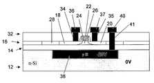
- FIG. 6a semiconductor device embodying the present invention is shown in which parts common to the device of FIG. 5 a are denoted by like reference numerals.
- a first semiconductor layer in the form of a silicon layer 16 in which an NMOS transistor is formedis covered by an insulating layer 32 , perforated by windows which are filled with conductive material to form contact areas 34 , 35 connected to the source 18 and drain 20 regions respectively.
- the contact areas 34 , 35are connected to conductive lines 36 , 37 respectively.
- the NMOS transistor of FIG. 6has a substrate layer 12 of n-type silicon having a second semiconductor layer in the form of a box region 38 of p-type silicon which is highly doped compared with the body 22 , but less highly doped than the corresponding source 18 and drain 20 .
- the box region 38is connected to a conductive line 40 by means of contact area 41 passing through insulating layer 14 , framework 28 and insulating layer 32 .
- An arrangement of transistors of this typecan be made using 0.13 ⁇ m technology, having an insulating layer 14 of thickness 400 nm and silicon layer 16 of thickness 30 nm. It should be noted that a single contact 41 can be used for a plurality of transistors of this type, and would typically be used for tens or hundreds of transistors.
- a negative voltageto box region 38 , typically in the region of ⁇ 20V for a layer 14 of thickness 400 nm, it is possible by means of the potential difference between gate 26 and box region 38 to form a neutral zone in the body 22 , similar to the neutral zone of the PD-SOI transistor of FIG. 4 . In this way, it is possible to generate, store and eliminate an electric charge in this neutral zone, the voltage necessary to create the neutral zone being reduced if the thickness of the layer 14 is reduced. Accordingly, such a transistor can be used to store a charge representing binary data, for example in a semiconductor DRAM memory or embedded memory device. A process for generating or eliminating electric charge in such a transistor is described in International patent application PCT/GB02/06495. In the regions of the device not provided with a box region 38 , it is possible to form conventional FD-SOI or PD-SOI transistors.
- FIGS. 7 a and 7 bin which parts common to the embodiment of FIG. 6 are denoted by like reference numerals, as an alternative to providing box region 38 to distort the valence and/or conduction band in the body 22 to increase the amount of charge which can be stored in the body 22 , it is possible to have a sufficiently large potential difference between the gate 26 and substrate layer 12 adjacent the body 22 to provide a charge storing neutral zone in the body 22 . This is achieved, for example, by applying a relatively large voltage shift (i.e. in the region of +20V) to each of the gate 26 , source 18 and drain 20 of the transistor.
- a relatively large voltage shifti.e. in the region of +20V
- FIG. 7 aillustrates a fully depleted (FD) SOI transistor biased in such a way as to behave like a normal FD device.
- FIG. 7 aapplying 2V on the gate 26 and 2V on the drain 20 , while the source 18 is kept at 0V turns on the transistor.
- FIG. 7 billustrates the same FD-SOI transistor behaving electrically like a partially depleted (PD) device.
- the addition of 20V on all device nodesdistorts the bands in such a way as to create a neutral region 23 in the transistor body 22 .
- 20Vis used when layer 14 is typically 400 nm thick. The respective voltage added is reduced proportionally in the case of a thinner layer 14 .
- FIG. 7 benables the charge storing neutral zone to be formed without the necessity of significantly altering the voltage of the substrate layer 12 , and requires fewer manufacturing steps than are necessary for the device shown in FIG. 6 .
- Thisalso provides the advantage that memory and logic devices can be formed on the same substrate, since although memory devices generally function correctly if a significant voltage shift is applied to the substrate, this is generally not the case for logic devices such as processors. Accordingly, the voltage shifts are applied to the memory devices but not to the logic devices.
- the box region 38is replaced by a highly doped region at the lower part of body 22 adjacent the insulating layer 14 , the source 18 and the drain 20 .
- a layercauses a similar effect to operation of the box region 38 of FIG. 6 .
- the energy bands of the body of the transistorare modified by doping more heavily a portion 25 of the body 22 .
- the body 22has therefore an upper part 21 with low doping content and a lower part 25 with a high doping content. This can be achieved by proper ion implantation, by epitaxy or by diffusion.
- the higher doping level of the lower body part 25distorts the bands in such a way as to create a region where the bands are flat, therefore creating a neutral region 23 .
- the present inventionallows transistors to be formed, the bodies of which can store an electric charge representing a binary data bit, in a silicon layer much narrower than in the prior art, with the advantage that the improved device performance of FD-SOI transistors is obtained.
Landscapes
- Semiconductor Memories (AREA)
- Thin Film Transistor (AREA)
- Dram (AREA)
Abstract
Description
- The present invention relates to semiconductor devices, and relates particularly, but not exclusively, to semiconductor charge storage devices such as semiconductor memories, and to substrates for manufacturing such devices.
- International patent application PCT/EP02/06495 discloses a DRAM (Dynamic Random Access Memory) device comprising a matrix of memory cells, each cell being formed by a field effect transistor. By applying suitable voltage pulses between the gate and drain and between the source and drain of each transistor, an electric charge can be generated and stored in the body of the transistor, the presence or absence of the charge representing a “1” or “0” state of a binary data bit. Memory devices using SOI (Silicon On Insulator) type field effect transistors are disclosed in more detail in “SOI technology: materials to VLSI”, second edition, Kluwer, Boston 1997.
- The transistors used in this type of device are PD-SOI (partially depleted silicon on insulator) transistors, which are formed in a layer of silicon formed on an insulating layer, the source, body and drain of each transistor being formed in the same layer, throughout the whole thickness of the silicon layer. The silicon layer is then covered by a dielectric film on which the gate of each transistor is formed.
- To enable a charge to be stored in the body of a transistor of this type, it is necessary for the body of the transistor to have a sufficiently thick layer of silicon at its central part to provide the silicon with a non-depleted region, known as the neutral region, the charge being stored in, or in the proximity of, this latter region. As a consequence, such transistors are known as partially depleted transistors.
- FD-SOI (fully depleted silicon on insulator) transistors are known, in which the silicon layer in which the source and drain regions are formed is thinner and/or the doping is less concentrated than in the case of partially depleted SOI transistors, as a result of which no neutral zone is provided. This means that it is not possible to store a charge in the body of such transistors. However, FD-SOI transistors present a number of advantages compared with partially depleted transistors, for example excellent short channel behaviour and a very rapid switching frequency. These advantages result from the small thickness of the silicon layer.
- A comparison of the construction of bulk and SOI transistors is shown in
FIGS. 1 and 2 . Referring toFIGS. 1 aand2a, an SOI transistor is formed from asubstrate 10 having asubstrate layer 12 of silicon, aninsulating layer 14 of silicon oxide or sapphire, and asilicon layer 16. In the case of a transistor using bulk technology, as shown inFIGS. 1 band2b, thesubstrate 10 comprises only thesilicon substrate layer 12. - Referring to
FIGS. 2 aand2b, in which parts common to both types of device are denoted by like reference numerals, integrated circuits comprising field effect transistors (of which only one is shown in each ofFIGS. 2 aand2b) are formed on thesubstrates 10 by successive photolithographic operations in which layers are partially removed, doped or new layers are deposited. The field effect transistor shown inFIG. 2 ahas asource 18 and adrain 20 formed inlayer 16, abody 22 being defined between thesource 16 anddrain 20, thesource 18 anddrain 20 extending through the full depth oflayer 16. As will be familiar to persons skilled in the art, thesource 18,drain 20 andbody 22 are formed by doping of the silicon oflayer 16. Thebody 22 is covered by adielectric film 24 overlapping withsource 18 anddrain 20, and on which agate 26 is provided. Thelayer 26 is removed around thesource 18 anddrain 20, and replaced by aninsulating framework 28 of silicon oxide. When a suitable voltage is applied to thegate 26, an electrically conductingchannel 30 connecting thesource 18 and drain20 forms at the surface of thebody 22 at the interface withdielectric film 24. - Referring to
FIG. 2 b, thesource 18 anddrain 20 are formed insubstrate layer 12 to define thebody 22 between the source and the drain, and thedielectric film 24 covers thebody 22 and overlaps thesource 18 anddrain 20. - Referring now to
FIGS. 3 aand3b,FIG. 3 bshows the variation of potential with thickness z (measured from the interface with dielectric film24) of region B in the bulk transistor ofFIG. 3 a. The graph shown inFIG. 3 bshows curves Bc, Byand Nf, representing the potential of the valence band, the conduction band and the Fermi level respectively at the interior ofbody 22. Similarly,FIGS. 4 aand4bshow corresponding diagrams for a PD-SOI transistor, andFIGS. 5 aand5bshow corresponding diagrams for a FD-SOI transistor. - It can be seen from
FIGS. 3 bto5bthat the valence band By and conduction band Bchave a minimum value of potential at the interface ofbody 22 anddielectric film 24 in the case of each type or transistor. However, it can be seen fromFIG. 3 bthat the potentials Bvand Bcvary in a first zone Zd, and tend towards a limiting value beyond which a second zone Zn, known as the neutral zone, starts. This second zone Znextends through the total thickness of thesubstrate layer 12. When a suitable voltage is applied togate 26, an electrically conductingchannel 30 forms at the surface of thebody 22 at the interface withdielectric film 24. - Referring now to
FIG. 4 b, it can be seen that the PD-SOI transistor has two depletion zones Zd1and Zd2, adjacentdielectric film 24 andinsulting layer 14 respectively, between which is located a neutral zone Zn. It will be appreciated by persons skilled in the art that the shape and extent of depletion zone Zd2depends upon the back gate potential relative to the front gate potential. It is possible to store an electric charge in thebody 22, in particular in, or in the proximity of, neutral zone Znlocated between the two depletion zones Zd1and Zd2. One possible application of such a transistor is as an individual memory cell, capable of representing two logic states depending upon the presence or absence of charge in or in the proximity of the neutral zone Zn, for forming a semiconductor memory device such as a DRAM. - Referring now to
FIG. 5 b, it can be seen that in the case of the FD-SOI transistor, the potential of the conduction band Bcand valence band Bvvaries continually throughout the entire thickness ofbody 22. In other words, thebody 22 has a depletion zone Zdextending throughout its entire thickness, as a result of which no neutral zone exists. It is therefore not possible to store charge in thebody 22, and the transistor of this type therefore cannot be used as a memory cell. However, transistors of this type have a number of advantages, in particular excellent short channel behaviour and a very rapid switching frequency, these properties being as a result of the small thickness oflayer 16. - Preferred embodiments of the present invention seek to combine the advantageous features of partially and fully depleted SOI transistors.
- According to an aspect of the present invention, there is provided a semiconductor device comprising:
- a substrate of semiconductor material;
- a first electrically insulating layer provided on said substrate;
- a first semiconductor layer provided on said first insulating layer and adapted to have respective source and drain regions of at least one field effect transistor formed therein to define a respective body region between said source and drain regions; and
- energy band modifying means for modifying the valence and/or conduction band in a said body region of at least one said field effect transistor to increase the amount of electrical charge which can be at least temporarily stored in said body region.
- By providing energy band modifying means for modifying the valence and/or conduction band of the body region of at least one said field effect transistor to increase the amount of electrical charge which can be stored in said body region, this provides the surprising advantage that the first semiconductor layer can be made considerably thinner than in the case of the prior art, which means that the advantages due to the thin layers of FD-SOI transistors (e.g., faster device performance) can be combined with the charge storing capability of PD-SOI transistors. For example, the present invention can be used to construct a particularly compact semiconductor memory device in which individual bits of data are represented by the presence or absence of charge stored in the body of individual transistors, while also utilising transistors of high performance.
- The energy band modifying means may be adapted to create a region in which an electrical charge can be at least temporarily stored in the body region of at least one said field effect transistor.
- In a preferred embodiment, the energy band modifying means is adapted to increase the length, in a direction substantially perpendicular to said first insulating layer, of a region in which the energy of said valence and conduction band in the body region of at least one said field effect transistor is substantially constant.
- The energy band modifying means may be adapted to apply a respective voltage change to a respective source, drain and at least one gate of at least one said field effect transistor.
- By applying voltage shifts to the source, drain and at least one gate of at least one said field effect transistor, this enables the charge storing capability of the invention to be achieved without significantly altering the substrate potential. This significantly improves the versatility of integrated devices formed from the device, for example by providing the advantage that charge storing memory devices can be located on the same substrate as logic devices, which latter devices generally cannot function if significant voltage shifts are applied to the substrate, and the voltage shifts applied to the memory devices only. The advantage is also provided that the device can be manufactured with the minimum number of manufacturing steps.
- In a preferred embodiment, the energy band modifying means comprises a doped portion of the body region of at least one said field effect transistor, wherein said doped portion is more heavily doped than the adjacent portion of the corresponding said body region.
- The doped portion may be arranged adjacent said first insulating layer.
- The energy band modifying means may comprise at least one second semiconductor layer arranged adjacent source and drain regions of at least one said field effect transistor in use and on a side of said first insulating layer remote from said first semiconductor layer.
- At least one said second semiconductor layer may at least partially cover said substrate.
- At least one said second semiconductor layer preferably forms part of said substrate.
- The device may further comprise contact means for connecting the or each said second semiconductor layer to a respective source of electrical input signals.
- The device may further comprise respective source and drain regions of at least one said field effect transistor formed in said first semiconductor layer to define a respective body region between said source and drain regions.
- The device may further comprise at least one respective gate of at least one said field effect transistor arranged adjacent the corresponding said body region of said field effect transistor.
- The device may further comprise a second insulating layer formed on said first semiconductor layer, and at least one respective gate region of at least one said field effect transistor arranged on said second insulating layer.
- In a preferred embodiment, the device is a semiconductor memory device.
- According to another aspect of the present invention, there is provided a method of controlling a semiconductor device comprising a substrate of semiconductor material, a first electrically insulating layer provided on said substrate, and a first semiconductor layer provided on said first insulating layer and having respective source and drain regions of at least one field effect transistor formed therein to define a respective body region between said source and drain regions, the method comprising modifying the valence and/or conduction band in a respective body region of at least one said field effect transistor to increase the amount of electrical charge which can be at least temporarily stored in said body region.
- The step of modifying said valence and/or conduction band may comprise applying a respective voltage change to a respective source, drain and at least one gate of said field effect transistor.
- The step of modifying said valence and/or conduction band may comprise applying a respective voltage to at least one second semiconductor layer located on a side of said first insulating layer remote from said first semiconductor layer.
- According to a further aspect of the present invention, there is provided a semiconductor wafer comprising:
- a substrate of doped semiconductor material;
- a first electrically insulating layer provided on said substrate;
- a first semiconductor layer provided on said first insulating; and
- at least one second layer of doped semiconductor material provided on a side of said first electrically insulating layer remote from said first semiconductor layer, wherein the or each said second semiconductor layer is more strongly doped than the respective region of said substrate adjacent thereto.
- Preferred embodiments of the invention will now be described, by way of example only and not in any limitative sense, with reference to the accompanying drawings, in which:
FIG. 1 ashows a schematic cross-sectional view of a known substrate for fabrication of integrated circuits using SOI technology;FIG. 1 bis a schematic cross-sectional view of a known substrate for fabrication of integrated circuits using bulk technology;FIG. 2 ais a schematic cross-sectional view of a known transistor formed from the substrate ofFIG. 1 a;FIG. 2 bis a cross-sectional view of a known transistor formed from the substrate ofFIG. 1 b;FIG. 3 ais a schematic cross-sectional view of the transistor ofFIG. 2 bshowing a region in which variation in potential is considered;FIG. 3 bis a graph illustrating the variation in potential in region B of the transistor ofFIG. 3 a;FIG. 4 ais a schematic cross-sectional view of the transistor ofFIG. 2 ausing PD-SOI technology;FIG. 4 bis a graph showing the variation of potential in region B of the transistor shown inFIG. 4 a;FIG. 5 ais a schematic cross-sectional view of the transistor orFIG. 2 ausing FD-SOI technology;FIG. 5 bis a graph showing the variation of potential in the region B of the transistor ofFIG. 5 a;FIG. 6 is a schematic cross-sectional view of a semiconductor device of a first embodiment of the present invention;FIG. 7 ais a schematic cross-sectional view of a semiconductor device of a second embodiment of the present invention, having unmodified energy bands;FIG. 7 bis a schematic cross-sectional view of the device ofFIG. 7 ahaving modified energy bands; andFIG. 8 is a schematic cross-sectional view of a semiconductor device of a third embodiment of the present invention.- Referring to
FIG. 6 , a semiconductor device embodying the present invention is shown in which parts common to the device ofFIG. 5 aare denoted by like reference numerals. A first semiconductor layer in the form of asilicon layer 16 in which an NMOS transistor is formed is covered by an insulatinglayer 32, perforated by windows which are filled with conductive material to formcontact areas source 18 and drain20 regions respectively. Thecontact areas conductive lines - The NMOS transistor of
FIG. 6 has asubstrate layer 12 of n-type silicon having a second semiconductor layer in the form of abox region 38 of p-type silicon which is highly doped compared with thebody 22, but less highly doped than thecorresponding source 18 anddrain 20. Thebox region 38 is connected to aconductive line 40 by means ofcontact area 41 passing through insulatinglayer 14,framework 28 and insulatinglayer 32. An arrangement of transistors of this type can be made using 0.13 μm technology, having an insulatinglayer 14 of thickness 400 nm andsilicon layer 16 ofthickness 30 nm. It should be noted that asingle contact 41 can be used for a plurality of transistors of this type, and would typically be used for tens or hundreds of transistors. - By applying a negative voltage to box
region 38, typically in the region of −20V for alayer 14 of thickness 400 nm, it is possible by means of the potential difference betweengate 26 andbox region 38 to form a neutral zone in thebody 22, similar to the neutral zone of the PD-SOI transistor ofFIG. 4 . In this way, it is possible to generate, store and eliminate an electric charge in this neutral zone, the voltage necessary to create the neutral zone being reduced if the thickness of thelayer 14 is reduced. Accordingly, such a transistor can be used to store a charge representing binary data, for example in a semiconductor DRAM memory or embedded memory device. A process for generating or eliminating electric charge in such a transistor is described in International patent application PCT/GB02/06495. In the regions of the device not provided with abox region 38, it is possible to form conventional FD-SOI or PD-SOI transistors. - Referring to
FIGS. 7 aand7b, in which parts common to the embodiment ofFIG. 6 are denoted by like reference numerals, as an alternative to providingbox region 38 to distort the valence and/or conduction band in thebody 22 to increase the amount of charge which can be stored in thebody 22, it is possible to have a sufficiently large potential difference between thegate 26 andsubstrate layer 12 adjacent thebody 22 to provide a charge storing neutral zone in thebody 22. This is achieved, for example, by applying a relatively large voltage shift (i.e. in the region of +20V) to each of thegate 26,source 18 and drain20 of the transistor. - In particular, as shown in
FIGS. 7 aand7b,FIG. 7 aillustrates a fully depleted (FD) SOI transistor biased in such a way as to behave like a normal FD device. InFIG. 7 a, applying 2V on thegate drain 20, while thesource 18 is kept at 0V turns on the transistor.FIG. 7 b, on the other hand, illustrates the same FD-SOI transistor behaving electrically like a partially depleted (PD) device. The addition of 20V on all device nodes distorts the bands in such a way as to create aneutral region 23 in thetransistor body 22. 20V is used whenlayer 14 is typically 400 nm thick. The respective voltage added is reduced proportionally in the case of athinner layer 14. - The arrangement of
FIG. 7 benables the charge storing neutral zone to be formed without the necessity of significantly altering the voltage of thesubstrate layer 12, and requires fewer manufacturing steps than are necessary for the device shown inFIG. 6 . This also provides the advantage that memory and logic devices can be formed on the same substrate, since although memory devices generally function correctly if a significant voltage shift is applied to the substrate, this is generally not the case for logic devices such as processors. Accordingly, the voltage shifts are applied to the memory devices but not to the logic devices. - Referring to
FIG. 8 , in which parts common to the embodiments ofFIGS. 6 and 7 are denoted by like reference numerals, thebox region 38 is replaced by a highly doped region at the lower part ofbody 22 adjacent the insulatinglayer 14, thesource 18 and thedrain 20. Such a layer causes a similar effect to operation of thebox region 38 ofFIG. 6 . In particular, the energy bands of the body of the transistor are modified by doping more heavily aportion 25 of thebody 22. This creates a doping gradient in the body. Thebody 22 has therefore anupper part 21 with low doping content and alower part 25 with a high doping content. This can be achieved by proper ion implantation, by epitaxy or by diffusion. The higher doping level of thelower body part 25 distorts the bands in such a way as to create a region where the bands are flat, therefore creating aneutral region 23. - It can therefore be seen that the present invention allows transistors to be formed, the bodies of which can store an electric charge representing a binary data bit, in a silicon layer much narrower than in the prior art, with the advantage that the improved device performance of FD-SOI transistors is obtained.
- It will be appreciated by persons skilled in the art that the above embodiment has been described by way of example only, and not in any limitative sense, and that various alterations and modifications are possible without departure from the scope of the invention as defined by the appended claims. Furthermore, it will be appreciated by persons skilled in the art that the above principle can be applied to PD-SOI type circuits when the thickness of the neutral zone is insufficient for the intended purpose of those circuits, and that the principle can be applied to PMOS type transistors as well as NMOS type transistors, in which case the polarities of the voltages used are opposite from those set out in the above-described embodiment.
Claims (25)
Priority Applications (1)
| Application Number | Priority Date | Filing Date | Title |
|---|---|---|---|
| US11/226,978US7514748B2 (en) | 2002-04-18 | 2005-09-15 | Semiconductor device |
Applications Claiming Priority (9)
| Application Number | Priority Date | Filing Date | Title |
|---|---|---|---|
| EPEP02405316.7 | 2002-04-18 | ||
| EP02405316AEP1355361A1 (en) | 2002-04-18 | 2002-04-18 | Method of forming an electric charge in a body of a semiconductor component |
| EP02405316 | 2002-04-18 | ||
| EP02078585AEP1357603A3 (en) | 2002-04-18 | 2002-08-27 | Semiconductor device |
| EPEP02078585.3 | 2002-08-27 | ||
| EP02078585 | 2002-08-27 | ||
| PCT/EP2003/002748WO2003088322A2 (en) | 2002-04-18 | 2003-03-17 | Semiconductor device |
| US10/487,157US7061050B2 (en) | 2002-04-18 | 2003-03-17 | Semiconductor device utilizing both fully and partially depleted devices |
| US11/226,978US7514748B2 (en) | 2002-04-18 | 2005-09-15 | Semiconductor device |
Related Parent Applications (3)
| Application Number | Title | Priority Date | Filing Date |
|---|---|---|---|
| PCT/EP2003/002748DivisionWO2003088322A2 (en) | 2002-04-18 | 2003-03-17 | Semiconductor device |
| US10487157Division | 2003-03-17 | ||
| US10/487,157DivisionUS7061050B2 (en) | 2002-04-18 | 2003-03-17 | Semiconductor device utilizing both fully and partially depleted devices |
Publications (2)
| Publication Number | Publication Date |
|---|---|
| US20060006468A1true US20060006468A1 (en) | 2006-01-12 |
| US7514748B2 US7514748B2 (en) | 2009-04-07 |
Family
ID=28793215
Family Applications (2)
| Application Number | Title | Priority Date | Filing Date |
|---|---|---|---|
| US10/487,157Expired - Fee RelatedUS7061050B2 (en) | 2002-04-18 | 2003-03-17 | Semiconductor device utilizing both fully and partially depleted devices |
| US11/226,978Expired - LifetimeUS7514748B2 (en) | 2002-04-18 | 2005-09-15 | Semiconductor device |
Family Applications Before (1)
| Application Number | Title | Priority Date | Filing Date |
|---|---|---|---|
| US10/487,157Expired - Fee RelatedUS7061050B2 (en) | 2002-04-18 | 2003-03-17 | Semiconductor device utilizing both fully and partially depleted devices |
Country Status (5)
| Country | Link |
|---|---|
| US (2) | US7061050B2 (en) |
| EP (1) | EP1357603A3 (en) |
| CN (1) | CN1647283A (en) |
| AU (1) | AU2003226646A1 (en) |
| WO (1) | WO2003088322A2 (en) |
Cited By (3)
| Publication number | Priority date | Publication date | Assignee | Title |
|---|---|---|---|---|
| US20100246285A1 (en)* | 2009-03-24 | 2010-09-30 | Micron Technology, Inc. | Methods, devices, and systems relating to a memory cell having a floating body |
| US20100254186A1 (en)* | 2009-04-07 | 2010-10-07 | Micron Technology, Inc. | Methods, devices, and systems relating to memory cells having a floating body |
| US20110134690A1 (en)* | 2009-12-08 | 2011-06-09 | Carlos Mazure | METHOD OF CONTROLLING A DRAM MEMORY CELL ON THE SeOI HAVING A SECOND CONTROL GATE BURIED UNDER THE INSULATING LAYER |
Families Citing this family (261)
| Publication number | Priority date | Publication date | Assignee | Title |
|---|---|---|---|---|
| US7710771B2 (en)* | 2002-11-20 | 2010-05-04 | The Regents Of The University Of California | Method and apparatus for capacitorless double-gate storage |
| US20040228168A1 (en) | 2003-05-13 | 2004-11-18 | Richard Ferrant | Semiconductor memory device and method of operating same |
| US6912150B2 (en) | 2003-05-13 | 2005-06-28 | Lionel Portman | Reference current generator, and method of programming, adjusting and/or operating same |
| US7518189B1 (en)* | 2003-07-03 | 2009-04-14 | American Semiconductor, Inc. | Independently-double-gated field effect transistor |
| US7335934B2 (en) | 2003-07-22 | 2008-02-26 | Innovative Silicon S.A. | Integrated circuit device, and method of fabricating same |
| US7184298B2 (en) | 2003-09-24 | 2007-02-27 | Innovative Silicon S.A. | Low power programming technique for a floating body memory transistor, memory cell, and memory array |
| JP2005116623A (en)* | 2003-10-03 | 2005-04-28 | Nec Electronics Corp | Semiconductor device and manufacturing method thereof |
| JP4511885B2 (en)* | 2004-07-09 | 2010-07-28 | Dowaエレクトロニクス株式会社 | Phosphor, LED and light source |
| US7238555B2 (en) | 2005-06-30 | 2007-07-03 | Freescale Semiconductor, Inc. | Single transistor memory cell with reduced programming voltages |
| US7517741B2 (en) | 2005-06-30 | 2009-04-14 | Freescale Semiconductor, Inc. | Single transistor memory cell with reduced recombination rates |
| US7709313B2 (en)* | 2005-07-19 | 2010-05-04 | International Business Machines Corporation | High performance capacitors in planar back gates CMOS |
| US7410856B2 (en) | 2006-09-14 | 2008-08-12 | Micron Technology, Inc. | Methods of forming vertical transistors |
| US7608898B2 (en) | 2006-10-31 | 2009-10-27 | Freescale Semiconductor, Inc. | One transistor DRAM cell structure |
| US7851859B2 (en)* | 2006-11-01 | 2010-12-14 | Samsung Electronics Co., Ltd. | Single transistor memory device having source and drain insulating regions and method of fabricating the same |
| KR100801707B1 (en)* | 2006-12-13 | 2008-02-11 | 삼성전자주식회사 | Floating Body Memory and Manufacturing Method Thereof |
| US7724578B2 (en)* | 2006-12-15 | 2010-05-25 | Globalfoundries Inc. | Sensing device for floating body cell memory and method thereof |
| US20080191788A1 (en)* | 2007-02-08 | 2008-08-14 | International Business Machines Corporation | Soi mosfet device with adjustable threshold voltage |
| JP5019436B2 (en)* | 2007-02-22 | 2012-09-05 | ルネサスエレクトロニクス株式会社 | Semiconductor integrated circuit |
| US8064274B2 (en) | 2007-05-30 | 2011-11-22 | Micron Technology, Inc. | Integrated circuit having voltage generation circuitry for memory cell array, and method of operating and/or controlling same |
| US20100027355A1 (en)* | 2007-07-31 | 2010-02-04 | Dao Thuy B | Planar double gate transistor storage cell |
| US20090078999A1 (en)* | 2007-09-20 | 2009-03-26 | Anderson Brent A | Semiconductor device structures with floating body charge storage and methods for forming such semiconductor device structures. |
| US7948008B2 (en)* | 2007-10-26 | 2011-05-24 | Micron Technology, Inc. | Floating body field-effect transistors, and methods of forming floating body field-effect transistors |
| KR101017809B1 (en)* | 2008-03-13 | 2011-02-28 | 주식회사 하이닉스반도체 | Semiconductor device and manufacturing method thereof |
| US7977172B2 (en)* | 2008-12-08 | 2011-07-12 | Advanced Micro Devices, Inc. | Dynamic random access memory (DRAM) cells and methods for fabricating the same |
| US8258810B2 (en) | 2010-09-30 | 2012-09-04 | Monolithic 3D Inc. | 3D semiconductor device |
| US8405420B2 (en) | 2009-04-14 | 2013-03-26 | Monolithic 3D Inc. | System comprising a semiconductor device and structure |
| US9509313B2 (en) | 2009-04-14 | 2016-11-29 | Monolithic 3D Inc. | 3D semiconductor device |
| US8058137B1 (en) | 2009-04-14 | 2011-11-15 | Monolithic 3D Inc. | Method for fabrication of a semiconductor device and structure |
| US8384426B2 (en) | 2009-04-14 | 2013-02-26 | Monolithic 3D Inc. | Semiconductor device and structure |
| US8669778B1 (en) | 2009-04-14 | 2014-03-11 | Monolithic 3D Inc. | Method for design and manufacturing of a 3D semiconductor device |
| US8362800B2 (en) | 2010-10-13 | 2013-01-29 | Monolithic 3D Inc. | 3D semiconductor device including field repairable logics |
| US9577642B2 (en) | 2009-04-14 | 2017-02-21 | Monolithic 3D Inc. | Method to form a 3D semiconductor device |
| US8754533B2 (en) | 2009-04-14 | 2014-06-17 | Monolithic 3D Inc. | Monolithic three-dimensional semiconductor device and structure |
| US8395191B2 (en) | 2009-10-12 | 2013-03-12 | Monolithic 3D Inc. | Semiconductor device and structure |
| US9711407B2 (en) | 2009-04-14 | 2017-07-18 | Monolithic 3D Inc. | Method of manufacturing a three dimensional integrated circuit by transfer of a mono-crystalline layer |
| US8373439B2 (en) | 2009-04-14 | 2013-02-12 | Monolithic 3D Inc. | 3D semiconductor device |
| US8427200B2 (en) | 2009-04-14 | 2013-04-23 | Monolithic 3D Inc. | 3D semiconductor device |
| US7986042B2 (en) | 2009-04-14 | 2011-07-26 | Monolithic 3D Inc. | Method for fabrication of a semiconductor device and structure |
| US8362482B2 (en) | 2009-04-14 | 2013-01-29 | Monolithic 3D Inc. | Semiconductor device and structure |
| US8378715B2 (en) | 2009-04-14 | 2013-02-19 | Monolithic 3D Inc. | Method to construct systems |
| US10043781B2 (en) | 2009-10-12 | 2018-08-07 | Monolithic 3D Inc. | 3D semiconductor device and structure |
| US8476145B2 (en) | 2010-10-13 | 2013-07-02 | Monolithic 3D Inc. | Method of fabricating a semiconductor device and structure |
| US12027518B1 (en) | 2009-10-12 | 2024-07-02 | Monolithic 3D Inc. | 3D semiconductor devices and structures with metal layers |
| US10366970B2 (en) | 2009-10-12 | 2019-07-30 | Monolithic 3D Inc. | 3D semiconductor device and structure |
| US8148728B2 (en) | 2009-10-12 | 2012-04-03 | Monolithic 3D, Inc. | Method for fabrication of a semiconductor device and structure |
| US10910364B2 (en) | 2009-10-12 | 2021-02-02 | Monolitaic 3D Inc. | 3D semiconductor device |
| US8450804B2 (en) | 2011-03-06 | 2013-05-28 | Monolithic 3D Inc. | Semiconductor device and structure for heat removal |
| US8536023B2 (en) | 2010-11-22 | 2013-09-17 | Monolithic 3D Inc. | Method of manufacturing a semiconductor device and structure |
| US10157909B2 (en) | 2009-10-12 | 2018-12-18 | Monolithic 3D Inc. | 3D semiconductor device and structure |
| US9099424B1 (en) | 2012-08-10 | 2015-08-04 | Monolithic 3D Inc. | Semiconductor system, device and structure with heat removal |
| US10354995B2 (en) | 2009-10-12 | 2019-07-16 | Monolithic 3D Inc. | Semiconductor memory device and structure |
| US8742476B1 (en) | 2012-11-27 | 2014-06-03 | Monolithic 3D Inc. | Semiconductor device and structure |
| US10388863B2 (en) | 2009-10-12 | 2019-08-20 | Monolithic 3D Inc. | 3D memory device and structure |
| US11018133B2 (en) | 2009-10-12 | 2021-05-25 | Monolithic 3D Inc. | 3D integrated circuit |
| US11984445B2 (en) | 2009-10-12 | 2024-05-14 | Monolithic 3D Inc. | 3D semiconductor devices and structures with metal layers |
| US8581349B1 (en) | 2011-05-02 | 2013-11-12 | Monolithic 3D Inc. | 3D memory semiconductor device and structure |
| US11374118B2 (en) | 2009-10-12 | 2022-06-28 | Monolithic 3D Inc. | Method to form a 3D integrated circuit |
| US8492838B2 (en) | 2009-11-16 | 2013-07-23 | International Business Machines Corporation | Isolation structures for SOI devices with ultrathin SOI and ultrathin box |
| FR2953641B1 (en) | 2009-12-08 | 2012-02-10 | S O I Tec Silicon On Insulator Tech | HOMOGENEOUS TRANSISTOR CIRCUIT ON SEOI WITH REAR CONTROL CHANNEL BURED UNDER THE INSULATING LAYER |
| US8508289B2 (en) | 2009-12-08 | 2013-08-13 | Soitec | Data-path cell on an SeOI substrate with a back control gate beneath the insulating layer |
| FR2953643B1 (en) | 2009-12-08 | 2012-07-27 | Soitec Silicon On Insulator | MEMORY CELL FLASH ON SEOI HAVING A SECOND CHECK GRID ENTERREE UNDER THE INSULATING LAYER |
| FR2957193B1 (en) | 2010-03-03 | 2012-04-20 | Soitec Silicon On Insulator | SEOI SUBSTRATE DATA PATH CELL WITH REAR CONTROL GRID BURED UNDER THE INSULATING LAYER |
| FR2955195B1 (en) | 2010-01-14 | 2012-03-09 | Soitec Silicon On Insulator | DEVICE FOR COMPARING DATA IN A MEMORY ADDRESSABLE BY CONTENT ON SEOI |
| FR2955200B1 (en) | 2010-01-14 | 2012-07-20 | Soitec Silicon On Insulator | DEVICE AND MANUFACTURING METHOD HAVING CONTACT BETWEEN SEMICONDUCTOR REGIONS THROUGH AN INSULATED INSULATED LAYER |
| FR2955203B1 (en) | 2010-01-14 | 2012-03-23 | Soitec Silicon On Insulator | MEMORY CELL WITH THE CHANNEL CROSSING A DIELECTRIC LAYER ENTERREE |
| FR2955204B1 (en) | 2010-01-14 | 2012-07-20 | Soitec Silicon On Insulator | DRAM MEMORY CELL HAVING A VERTICAL BIPOLAR INJECTOR |
| US8541819B1 (en) | 2010-12-09 | 2013-09-24 | Monolithic 3D Inc. | Semiconductor device and structure |
| US8492886B2 (en) | 2010-02-16 | 2013-07-23 | Monolithic 3D Inc | 3D integrated circuit with logic |
| US8026521B1 (en) | 2010-10-11 | 2011-09-27 | Monolithic 3D Inc. | Semiconductor device and structure |
| US8298875B1 (en) | 2011-03-06 | 2012-10-30 | Monolithic 3D Inc. | Method for fabrication of a semiconductor device and structure |
| US8373230B1 (en) | 2010-10-13 | 2013-02-12 | Monolithic 3D Inc. | Method for fabrication of a semiconductor device and structure |
| US8461035B1 (en) | 2010-09-30 | 2013-06-11 | Monolithic 3D Inc. | Method for fabrication of a semiconductor device and structure |
| US9099526B2 (en) | 2010-02-16 | 2015-08-04 | Monolithic 3D Inc. | Integrated circuit device and structure |
| FR2957186B1 (en) | 2010-03-08 | 2012-09-28 | Soitec Silicon On Insulator | MEMORY CELL OF SRAM TYPE |
| FR2957449B1 (en) | 2010-03-11 | 2022-07-15 | S O I Tec Silicon On Insulator Tech | READOUT MICRO-AMPLIFIER FOR MEMORY |
| FR2958441B1 (en) | 2010-04-02 | 2012-07-13 | Soitec Silicon On Insulator | PSEUDO-INVERTER CIRCUIT ON SEOI |
| EP2375442A1 (en) | 2010-04-06 | 2011-10-12 | S.O.I.Tec Silicon on Insulator Technologies | Method for manufacturing a semiconductor substrate |
| EP2381470B1 (en) | 2010-04-22 | 2012-08-22 | Soitec | Semiconductor device comprising a field-effect transistor in a silicon-on-insulator structure |
| US9219005B2 (en) | 2011-06-28 | 2015-12-22 | Monolithic 3D Inc. | Semiconductor system and device |
| US9953925B2 (en) | 2011-06-28 | 2018-04-24 | Monolithic 3D Inc. | Semiconductor system and device |
| US8642416B2 (en) | 2010-07-30 | 2014-02-04 | Monolithic 3D Inc. | Method of forming three dimensional integrated circuit devices using layer transfer technique |
| US10217667B2 (en) | 2011-06-28 | 2019-02-26 | Monolithic 3D Inc. | 3D semiconductor device, fabrication method and system |
| US8901613B2 (en) | 2011-03-06 | 2014-12-02 | Monolithic 3D Inc. | Semiconductor device and structure for heat removal |
| US10497713B2 (en) | 2010-11-18 | 2019-12-03 | Monolithic 3D Inc. | 3D semiconductor memory device and structure |
| US12362219B2 (en) | 2010-11-18 | 2025-07-15 | Monolithic 3D Inc. | 3D semiconductor memory device and structure |
| US8273610B2 (en) | 2010-11-18 | 2012-09-25 | Monolithic 3D Inc. | Method of constructing a semiconductor device and structure |
| US11482440B2 (en) | 2010-12-16 | 2022-10-25 | Monolithic 3D Inc. | 3D semiconductor device and structure with a built-in test circuit for repairing faulty circuits |
| US8163581B1 (en) | 2010-10-13 | 2012-04-24 | Monolith IC 3D | Semiconductor and optoelectronic devices |
| US11018191B1 (en) | 2010-10-11 | 2021-05-25 | Monolithic 3D Inc. | 3D semiconductor device and structure |
| US11227897B2 (en) | 2010-10-11 | 2022-01-18 | Monolithic 3D Inc. | Method for producing a 3D semiconductor memory device and structure |
| US11158674B2 (en) | 2010-10-11 | 2021-10-26 | Monolithic 3D Inc. | Method to produce a 3D semiconductor device and structure |
| US10290682B2 (en) | 2010-10-11 | 2019-05-14 | Monolithic 3D Inc. | 3D IC semiconductor device and structure with stacked memory |
| US11024673B1 (en) | 2010-10-11 | 2021-06-01 | Monolithic 3D Inc. | 3D semiconductor device and structure |
| US11600667B1 (en) | 2010-10-11 | 2023-03-07 | Monolithic 3D Inc. | Method to produce 3D semiconductor devices and structures with memory |
| US10896931B1 (en) | 2010-10-11 | 2021-01-19 | Monolithic 3D Inc. | 3D semiconductor device and structure |
| US8114757B1 (en) | 2010-10-11 | 2012-02-14 | Monolithic 3D Inc. | Semiconductor device and structure |
| US11469271B2 (en) | 2010-10-11 | 2022-10-11 | Monolithic 3D Inc. | Method to produce 3D semiconductor devices and structures with memory |
| US11315980B1 (en) | 2010-10-11 | 2022-04-26 | Monolithic 3D Inc. | 3D semiconductor device and structure with transistors |
| US11257867B1 (en) | 2010-10-11 | 2022-02-22 | Monolithic 3D Inc. | 3D semiconductor device and structure with oxide bonds |
| US11043523B1 (en) | 2010-10-13 | 2021-06-22 | Monolithic 3D Inc. | Multilevel semiconductor device and structure with image sensors |
| US11327227B2 (en) | 2010-10-13 | 2022-05-10 | Monolithic 3D Inc. | Multilevel semiconductor device and structure with electromagnetic modulators |
| US11855100B2 (en) | 2010-10-13 | 2023-12-26 | Monolithic 3D Inc. | Multilevel semiconductor device and structure with oxide bonding |
| US11404466B2 (en) | 2010-10-13 | 2022-08-02 | Monolithic 3D Inc. | Multilevel semiconductor device and structure with image sensors |
| US11855114B2 (en) | 2010-10-13 | 2023-12-26 | Monolithic 3D Inc. | Multilevel semiconductor device and structure with image sensors and wafer bonding |
| US11869915B2 (en) | 2010-10-13 | 2024-01-09 | Monolithic 3D Inc. | Multilevel semiconductor device and structure with image sensors and wafer bonding |
| US11133344B2 (en) | 2010-10-13 | 2021-09-28 | Monolithic 3D Inc. | Multilevel semiconductor device and structure with image sensors |
| US12080743B2 (en) | 2010-10-13 | 2024-09-03 | Monolithic 3D Inc. | Multilevel semiconductor device and structure with image sensors and wafer bonding |
| US11929372B2 (en) | 2010-10-13 | 2024-03-12 | Monolithic 3D Inc. | Multilevel semiconductor device and structure with image sensors and wafer bonding |
| US9197804B1 (en) | 2011-10-14 | 2015-11-24 | Monolithic 3D Inc. | Semiconductor and optoelectronic devices |
| US12094892B2 (en) | 2010-10-13 | 2024-09-17 | Monolithic 3D Inc. | 3D micro display device and structure |
| US11164898B2 (en) | 2010-10-13 | 2021-11-02 | Monolithic 3D Inc. | Multilevel semiconductor device and structure |
| US11605663B2 (en) | 2010-10-13 | 2023-03-14 | Monolithic 3D Inc. | Multilevel semiconductor device and structure with image sensors and wafer bonding |
| US11063071B1 (en) | 2010-10-13 | 2021-07-13 | Monolithic 3D Inc. | Multilevel semiconductor device and structure with waveguides |
| US11163112B2 (en) | 2010-10-13 | 2021-11-02 | Monolithic 3D Inc. | Multilevel semiconductor device and structure with electromagnetic modulators |
| US12360310B2 (en) | 2010-10-13 | 2025-07-15 | Monolithic 3D Inc. | Multilevel semiconductor device and structure with oxide bonding |
| US10679977B2 (en) | 2010-10-13 | 2020-06-09 | Monolithic 3D Inc. | 3D microdisplay device and structure |
| US11694922B2 (en) | 2010-10-13 | 2023-07-04 | Monolithic 3D Inc. | Multilevel semiconductor device and structure with oxide bonding |
| US10833108B2 (en) | 2010-10-13 | 2020-11-10 | Monolithic 3D Inc. | 3D microdisplay device and structure |
| US8283215B2 (en) | 2010-10-13 | 2012-10-09 | Monolithic 3D Inc. | Semiconductor and optoelectronic devices |
| US8379458B1 (en) | 2010-10-13 | 2013-02-19 | Monolithic 3D Inc. | Semiconductor device and structure |
| US10943934B2 (en) | 2010-10-13 | 2021-03-09 | Monolithic 3D Inc. | Multilevel semiconductor device and structure |
| US11437368B2 (en) | 2010-10-13 | 2022-09-06 | Monolithic 3D Inc. | Multilevel semiconductor device and structure with oxide bonding |
| US10978501B1 (en) | 2010-10-13 | 2021-04-13 | Monolithic 3D Inc. | Multilevel semiconductor device and structure with waveguides |
| US10998374B1 (en) | 2010-10-13 | 2021-05-04 | Monolithic 3D Inc. | Multilevel semiconductor device and structure |
| US11984438B2 (en) | 2010-10-13 | 2024-05-14 | Monolithic 3D Inc. | Multilevel semiconductor device and structure with oxide bonding |
| US11495484B2 (en) | 2010-11-18 | 2022-11-08 | Monolithic 3D Inc. | 3D semiconductor devices and structures with at least two single-crystal layers |
| US11804396B2 (en) | 2010-11-18 | 2023-10-31 | Monolithic 3D Inc. | Methods for producing a 3D semiconductor device and structure with memory cells and multiple metal layers |
| US12033884B2 (en) | 2010-11-18 | 2024-07-09 | Monolithic 3D Inc. | Methods for producing a 3D semiconductor device and structure with memory cells and multiple metal layers |
| US11004719B1 (en) | 2010-11-18 | 2021-05-11 | Monolithic 3D Inc. | Methods for producing a 3D semiconductor memory device and structure |
| US11107721B2 (en) | 2010-11-18 | 2021-08-31 | Monolithic 3D Inc. | 3D semiconductor device and structure with NAND logic |
| US11482439B2 (en) | 2010-11-18 | 2022-10-25 | Monolithic 3D Inc. | Methods for producing a 3D semiconductor memory device comprising charge trap junction-less transistors |
| US11211279B2 (en) | 2010-11-18 | 2021-12-28 | Monolithic 3D Inc. | Method for processing a 3D integrated circuit and structure |
| US11031275B2 (en) | 2010-11-18 | 2021-06-08 | Monolithic 3D Inc. | 3D semiconductor device and structure with memory |
| US11854857B1 (en) | 2010-11-18 | 2023-12-26 | Monolithic 3D Inc. | Methods for producing a 3D semiconductor device and structure with memory cells and multiple metal layers |
| US12136562B2 (en) | 2010-11-18 | 2024-11-05 | Monolithic 3D Inc. | 3D semiconductor device and structure with single-crystal layers |
| US11018042B1 (en) | 2010-11-18 | 2021-05-25 | Monolithic 3D Inc. | 3D semiconductor memory device and structure |
| US12154817B1 (en) | 2010-11-18 | 2024-11-26 | Monolithic 3D Inc. | Methods for producing a 3D semiconductor memory device and structure |
| US12243765B2 (en) | 2010-11-18 | 2025-03-04 | Monolithic 3D Inc. | 3D semiconductor device and structure with metal layers and memory cells |
| US11615977B2 (en) | 2010-11-18 | 2023-03-28 | Monolithic 3D Inc. | 3D semiconductor memory device and structure |
| US11862503B2 (en) | 2010-11-18 | 2024-01-02 | Monolithic 3D Inc. | Method for producing a 3D semiconductor device and structure with memory cells and multiple metal layers |
| US11508605B2 (en) | 2010-11-18 | 2022-11-22 | Monolithic 3D Inc. | 3D semiconductor memory device and structure |
| US11164770B1 (en) | 2010-11-18 | 2021-11-02 | Monolithic 3D Inc. | Method for producing a 3D semiconductor memory device and structure |
| US11923230B1 (en) | 2010-11-18 | 2024-03-05 | Monolithic 3D Inc. | 3D semiconductor device and structure with bonding |
| US11443971B2 (en) | 2010-11-18 | 2022-09-13 | Monolithic 3D Inc. | 3D semiconductor device and structure with memory |
| US11094576B1 (en) | 2010-11-18 | 2021-08-17 | Monolithic 3D Inc. | Methods for producing a 3D semiconductor memory device and structure |
| US11521888B2 (en) | 2010-11-18 | 2022-12-06 | Monolithic 3D Inc. | 3D semiconductor device and structure with high-k metal gate transistors |
| US11610802B2 (en) | 2010-11-18 | 2023-03-21 | Monolithic 3D Inc. | Method for producing a 3D semiconductor device and structure with single crystal transistors and metal gate electrodes |
| US11569117B2 (en) | 2010-11-18 | 2023-01-31 | Monolithic 3D Inc. | 3D semiconductor device and structure with single-crystal layers |
| US12068187B2 (en) | 2010-11-18 | 2024-08-20 | Monolithic 3D Inc. | 3D semiconductor device and structure with bonding and DRAM memory cells |
| US11735462B2 (en) | 2010-11-18 | 2023-08-22 | Monolithic 3D Inc. | 3D semiconductor device and structure with single-crystal layers |
| US11784082B2 (en) | 2010-11-18 | 2023-10-10 | Monolithic 3D Inc. | 3D semiconductor device and structure with bonding |
| US12100611B2 (en) | 2010-11-18 | 2024-09-24 | Monolithic 3D Inc. | Methods for producing a 3D semiconductor device and structure with memory cells and multiple metal layers |
| US11482438B2 (en) | 2010-11-18 | 2022-10-25 | Monolithic 3D Inc. | Methods for producing a 3D semiconductor memory device and structure |
| US11901210B2 (en) | 2010-11-18 | 2024-02-13 | Monolithic 3D Inc. | 3D semiconductor device and structure with memory |
| US12272586B2 (en) | 2010-11-18 | 2025-04-08 | Monolithic 3D Inc. | 3D semiconductor memory device and structure with memory and metal layers |
| US11355381B2 (en) | 2010-11-18 | 2022-06-07 | Monolithic 3D Inc. | 3D semiconductor memory device and structure |
| US11355380B2 (en) | 2010-11-18 | 2022-06-07 | Monolithic 3D Inc. | Methods for producing 3D semiconductor memory device and structure utilizing alignment marks |
| US11121021B2 (en) | 2010-11-18 | 2021-09-14 | Monolithic 3D Inc. | 3D semiconductor device and structure |
| US12144190B2 (en) | 2010-11-18 | 2024-11-12 | Monolithic 3D Inc. | 3D semiconductor device and structure with bonding and memory cells preliminary class |
| US12125737B1 (en) | 2010-11-18 | 2024-10-22 | Monolithic 3D Inc. | 3D semiconductor device and structure with metal layers and memory cells |
| US8975670B2 (en) | 2011-03-06 | 2015-03-10 | Monolithic 3D Inc. | Semiconductor device and structure for heat removal |
| US10388568B2 (en) | 2011-06-28 | 2019-08-20 | Monolithic 3D Inc. | 3D semiconductor device and system |
| US8687399B2 (en) | 2011-10-02 | 2014-04-01 | Monolithic 3D Inc. | Semiconductor device and structure |
| US9029173B2 (en) | 2011-10-18 | 2015-05-12 | Monolithic 3D Inc. | Method for fabrication of a semiconductor device and structure |
| US9000557B2 (en) | 2012-03-17 | 2015-04-07 | Zvi Or-Bach | Semiconductor device and structure |
| US10600888B2 (en) | 2012-04-09 | 2020-03-24 | Monolithic 3D Inc. | 3D semiconductor device |
| US11694944B1 (en) | 2012-04-09 | 2023-07-04 | Monolithic 3D Inc. | 3D semiconductor device and structure with metal layers and a connective path |
| US11616004B1 (en) | 2012-04-09 | 2023-03-28 | Monolithic 3D Inc. | 3D semiconductor device and structure with metal layers and a connective path |
| US11594473B2 (en) | 2012-04-09 | 2023-02-28 | Monolithic 3D Inc. | 3D semiconductor device and structure with metal layers and a connective path |
| US11735501B1 (en) | 2012-04-09 | 2023-08-22 | Monolithic 3D Inc. | 3D semiconductor device and structure with metal layers and a connective path |
| US11410912B2 (en) | 2012-04-09 | 2022-08-09 | Monolithic 3D Inc. | 3D semiconductor device with vias and isolation layers |
| US11164811B2 (en) | 2012-04-09 | 2021-11-02 | Monolithic 3D Inc. | 3D semiconductor device with isolation layers and oxide-to-oxide bonding |
| US8557632B1 (en) | 2012-04-09 | 2013-10-15 | Monolithic 3D Inc. | Method for fabrication of a semiconductor device and structure |
| US11088050B2 (en) | 2012-04-09 | 2021-08-10 | Monolithic 3D Inc. | 3D semiconductor device with isolation layers |
| US11476181B1 (en) | 2012-04-09 | 2022-10-18 | Monolithic 3D Inc. | 3D semiconductor device and structure with metal layers |
| US11881443B2 (en) | 2012-04-09 | 2024-01-23 | Monolithic 3D Inc. | 3D semiconductor device and structure with metal layers and a connective path |
| US8686428B1 (en) | 2012-11-16 | 2014-04-01 | Monolithic 3D Inc. | Semiconductor device and structure |
| US8574929B1 (en) | 2012-11-16 | 2013-11-05 | Monolithic 3D Inc. | Method to form a 3D semiconductor device and structure |
| US11217565B2 (en) | 2012-12-22 | 2022-01-04 | Monolithic 3D Inc. | Method to form a 3D semiconductor device and structure |
| US11018116B2 (en) | 2012-12-22 | 2021-05-25 | Monolithic 3D Inc. | Method to form a 3D semiconductor device and structure |
| US11961827B1 (en) | 2012-12-22 | 2024-04-16 | Monolithic 3D Inc. | 3D semiconductor device and structure with metal layers |
| US11063024B1 (en) | 2012-12-22 | 2021-07-13 | Monlithic 3D Inc. | Method to form a 3D semiconductor device and structure |
| US8674470B1 (en) | 2012-12-22 | 2014-03-18 | Monolithic 3D Inc. | Semiconductor device and structure |
| US11784169B2 (en) | 2012-12-22 | 2023-10-10 | Monolithic 3D Inc. | 3D semiconductor device and structure with metal layers |
| US11967583B2 (en) | 2012-12-22 | 2024-04-23 | Monolithic 3D Inc. | 3D semiconductor device and structure with metal layers |
| US11916045B2 (en) | 2012-12-22 | 2024-02-27 | Monolithic 3D Inc. | 3D semiconductor device and structure with metal layers |
| US12051674B2 (en) | 2012-12-22 | 2024-07-30 | Monolithic 3D Inc. | 3D semiconductor device and structure with metal layers |
| US11309292B2 (en) | 2012-12-22 | 2022-04-19 | Monolithic 3D Inc. | 3D semiconductor device and structure with metal layers |
| US10115663B2 (en) | 2012-12-29 | 2018-10-30 | Monolithic 3D Inc. | 3D semiconductor device and structure |
| US11087995B1 (en) | 2012-12-29 | 2021-08-10 | Monolithic 3D Inc. | 3D semiconductor device and structure |
| US11430667B2 (en) | 2012-12-29 | 2022-08-30 | Monolithic 3D Inc. | 3D semiconductor device and structure with bonding |
| US11177140B2 (en) | 2012-12-29 | 2021-11-16 | Monolithic 3D Inc. | 3D semiconductor device and structure |
| US11430668B2 (en) | 2012-12-29 | 2022-08-30 | Monolithic 3D Inc. | 3D semiconductor device and structure with bonding |
| US9871034B1 (en) | 2012-12-29 | 2018-01-16 | Monolithic 3D Inc. | Semiconductor device and structure |
| US10600657B2 (en) | 2012-12-29 | 2020-03-24 | Monolithic 3D Inc | 3D semiconductor device and structure |
| US12249538B2 (en) | 2012-12-29 | 2025-03-11 | Monolithic 3D Inc. | 3D semiconductor device and structure including power distribution grids |
| US10892169B2 (en) | 2012-12-29 | 2021-01-12 | Monolithic 3D Inc. | 3D semiconductor device and structure |
| US9385058B1 (en) | 2012-12-29 | 2016-07-05 | Monolithic 3D Inc. | Semiconductor device and structure |
| US10903089B1 (en) | 2012-12-29 | 2021-01-26 | Monolithic 3D Inc. | 3D semiconductor device and structure |
| US11004694B1 (en) | 2012-12-29 | 2021-05-11 | Monolithic 3D Inc. | 3D semiconductor device and structure |
| US10651054B2 (en) | 2012-12-29 | 2020-05-12 | Monolithic 3D Inc. | 3D semiconductor device and structure |
| US12094965B2 (en) | 2013-03-11 | 2024-09-17 | Monolithic 3D Inc. | 3D semiconductor device and structure with metal layers and memory cells |
| US10325651B2 (en) | 2013-03-11 | 2019-06-18 | Monolithic 3D Inc. | 3D semiconductor device with stacked memory |
| US11869965B2 (en) | 2013-03-11 | 2024-01-09 | Monolithic 3D Inc. | 3D semiconductor device and structure with metal layers and memory cells |
| US8902663B1 (en) | 2013-03-11 | 2014-12-02 | Monolithic 3D Inc. | Method of maintaining a memory state |
| US11935949B1 (en) | 2013-03-11 | 2024-03-19 | Monolithic 3D Inc. | 3D semiconductor device and structure with metal layers and memory cells |
| US12100646B2 (en) | 2013-03-12 | 2024-09-24 | Monolithic 3D Inc. | 3D semiconductor device and structure with metal layers |
| US11398569B2 (en) | 2013-03-12 | 2022-07-26 | Monolithic 3D Inc. | 3D semiconductor device and structure |
| US8994404B1 (en) | 2013-03-12 | 2015-03-31 | Monolithic 3D Inc. | Semiconductor device and structure |
| US10840239B2 (en) | 2014-08-26 | 2020-11-17 | Monolithic 3D Inc. | 3D semiconductor device and structure |
| US11088130B2 (en) | 2014-01-28 | 2021-08-10 | Monolithic 3D Inc. | 3D semiconductor device and structure |
| US11923374B2 (en) | 2013-03-12 | 2024-03-05 | Monolithic 3D Inc. | 3D semiconductor device and structure with metal layers |
| US10224279B2 (en) | 2013-03-15 | 2019-03-05 | Monolithic 3D Inc. | Semiconductor device and structure |
| US9117749B1 (en) | 2013-03-15 | 2015-08-25 | Monolithic 3D Inc. | Semiconductor device and structure |
| US11270055B1 (en) | 2013-04-15 | 2022-03-08 | Monolithic 3D Inc. | Automation for monolithic 3D devices |
| US11030371B2 (en) | 2013-04-15 | 2021-06-08 | Monolithic 3D Inc. | Automation for monolithic 3D devices |
| US9021414B1 (en) | 2013-04-15 | 2015-04-28 | Monolithic 3D Inc. | Automation for monolithic 3D devices |
| US11487928B2 (en) | 2013-04-15 | 2022-11-01 | Monolithic 3D Inc. | Automation for monolithic 3D devices |
| US11341309B1 (en) | 2013-04-15 | 2022-05-24 | Monolithic 3D Inc. | Automation for monolithic 3D devices |
| US11574109B1 (en) | 2013-04-15 | 2023-02-07 | Monolithic 3D Inc | Automation methods for 3D integrated circuits and devices |
| US11720736B2 (en) | 2013-04-15 | 2023-08-08 | Monolithic 3D Inc. | Automation methods for 3D integrated circuits and devices |
| US20150129967A1 (en) | 2013-11-12 | 2015-05-14 | Stmicroelectronics International N.V. | Dual gate fd-soi transistor |
| US10297586B2 (en) | 2015-03-09 | 2019-05-21 | Monolithic 3D Inc. | Methods for processing a 3D semiconductor device |
| US11031394B1 (en) | 2014-01-28 | 2021-06-08 | Monolithic 3D Inc. | 3D semiconductor device and structure |
| US11107808B1 (en) | 2014-01-28 | 2021-08-31 | Monolithic 3D Inc. | 3D semiconductor device and structure |
| US12094829B2 (en) | 2014-01-28 | 2024-09-17 | Monolithic 3D Inc. | 3D semiconductor device and structure |
| US9800204B2 (en) | 2014-03-19 | 2017-10-24 | Stmicroelectronics International N.V. | Integrated circuit capacitor including dual gate silicon-on-insulator transistor |
| US11011507B1 (en) | 2015-04-19 | 2021-05-18 | Monolithic 3D Inc. | 3D semiconductor device and structure |
| US10825779B2 (en) | 2015-04-19 | 2020-11-03 | Monolithic 3D Inc. | 3D semiconductor device and structure |
| US11056468B1 (en) | 2015-04-19 | 2021-07-06 | Monolithic 3D Inc. | 3D semiconductor device and structure |
| US10381328B2 (en) | 2015-04-19 | 2019-08-13 | Monolithic 3D Inc. | Semiconductor device and structure |
| US11956952B2 (en) | 2015-08-23 | 2024-04-09 | Monolithic 3D Inc. | Semiconductor memory device and structure |
| US11978731B2 (en) | 2015-09-21 | 2024-05-07 | Monolithic 3D Inc. | Method to produce a multi-level semiconductor memory device and structure |
| US12250830B2 (en) | 2015-09-21 | 2025-03-11 | Monolithic 3D Inc. | 3D semiconductor memory devices and structures |
| US11114427B2 (en) | 2015-11-07 | 2021-09-07 | Monolithic 3D Inc. | 3D semiconductor processor and memory device and structure |
| US12178055B2 (en) | 2015-09-21 | 2024-12-24 | Monolithic 3D Inc. | 3D semiconductor memory devices and structures |
| US12100658B2 (en) | 2015-09-21 | 2024-09-24 | Monolithic 3D Inc. | Method to produce a 3D multilayer semiconductor device and structure |
| CN108401468A (en) | 2015-09-21 | 2018-08-14 | 莫诺利特斯3D有限公司 | 3D semiconductor devices and structures |
| US11937422B2 (en) | 2015-11-07 | 2024-03-19 | Monolithic 3D Inc. | Semiconductor memory device and structure |
| US10522225B1 (en) | 2015-10-02 | 2019-12-31 | Monolithic 3D Inc. | Semiconductor device with non-volatile memory |
| US11991884B1 (en) | 2015-10-24 | 2024-05-21 | Monolithic 3D Inc. | 3D semiconductor device and structure with logic and memory |
| US12120880B1 (en) | 2015-10-24 | 2024-10-15 | Monolithic 3D Inc. | 3D semiconductor device and structure with logic and memory |
| US11296115B1 (en) | 2015-10-24 | 2022-04-05 | Monolithic 3D Inc. | 3D semiconductor device and structure |
| US12035531B2 (en) | 2015-10-24 | 2024-07-09 | Monolithic 3D Inc. | 3D semiconductor device and structure with logic and memory |
| US11114464B2 (en) | 2015-10-24 | 2021-09-07 | Monolithic 3D Inc. | 3D semiconductor device and structure |
| US10847540B2 (en) | 2015-10-24 | 2020-11-24 | Monolithic 3D Inc. | 3D semiconductor memory device and structure |
| US12219769B2 (en) | 2015-10-24 | 2025-02-04 | Monolithic 3D Inc. | 3D semiconductor device and structure with logic and memory |
| US12016181B2 (en) | 2015-10-24 | 2024-06-18 | Monolithic 3D Inc. | 3D semiconductor device and structure with logic and memory |
| US10418369B2 (en) | 2015-10-24 | 2019-09-17 | Monolithic 3D Inc. | Multi-level semiconductor memory device and structure |
| US12225704B2 (en) | 2016-10-10 | 2025-02-11 | Monolithic 3D Inc. | 3D memory devices and structures with memory arrays and metal layers |
| US11329059B1 (en) | 2016-10-10 | 2022-05-10 | Monolithic 3D Inc. | 3D memory devices and structures with thinned single crystal substrates |
| US11251149B2 (en) | 2016-10-10 | 2022-02-15 | Monolithic 3D Inc. | 3D memory device and structure |
| US11812620B2 (en) | 2016-10-10 | 2023-11-07 | Monolithic 3D Inc. | 3D DRAM memory devices and structures with control circuits |
| US11930648B1 (en) | 2016-10-10 | 2024-03-12 | Monolithic 3D Inc. | 3D memory devices and structures with metal layers |
| US11711928B2 (en) | 2016-10-10 | 2023-07-25 | Monolithic 3D Inc. | 3D memory devices and structures with control circuits |
| US11869591B2 (en) | 2016-10-10 | 2024-01-09 | Monolithic 3D Inc. | 3D memory devices and structures with control circuits |
| US11763864B2 (en) | 2019-04-08 | 2023-09-19 | Monolithic 3D Inc. | 3D memory semiconductor devices and structures with bit-line pillars |
| US11158652B1 (en) | 2019-04-08 | 2021-10-26 | Monolithic 3D Inc. | 3D memory semiconductor devices and structures |
| US11296106B2 (en) | 2019-04-08 | 2022-04-05 | Monolithic 3D Inc. | 3D memory semiconductor devices and structures |
| US10892016B1 (en) | 2019-04-08 | 2021-01-12 | Monolithic 3D Inc. | 3D memory semiconductor devices and structures |
| US11018156B2 (en) | 2019-04-08 | 2021-05-25 | Monolithic 3D Inc. | 3D memory semiconductor devices and structures |
Citations (18)
| Publication number | Priority date | Publication date | Assignee | Title |
|---|---|---|---|---|
| US3439214A (en)* | 1968-03-04 | 1969-04-15 | Fairchild Camera Instr Co | Beam-junction scan converter |
| US3997799A (en)* | 1975-09-15 | 1976-12-14 | Baker Roger T | Semiconductor-device for the storage of binary data |
| US4032947A (en)* | 1971-10-20 | 1977-06-28 | Siemens Aktiengesellschaft | Controllable charge-coupled semiconductor device |
| US4298962A (en)* | 1979-01-25 | 1981-11-03 | Nippon Electric Co., Ltd. | Memory |
| US4979014A (en)* | 1987-08-10 | 1990-12-18 | Kabushiki Kaisha Toshiba | MOS transistor |
| US5144390A (en)* | 1988-09-02 | 1992-09-01 | Texas Instruments Incorporated | Silicon-on insulator transistor with internal body node to source node connection |
| US5448513A (en)* | 1993-12-02 | 1995-09-05 | Regents Of The University Of California | Capacitorless DRAM device on silicon-on-insulator substrate |
| US5489792A (en)* | 1994-04-07 | 1996-02-06 | Regents Of The University Of California | Silicon-on-insulator transistors having improved current characteristics and reduced electrostatic discharge susceptibility |
| US5696718A (en)* | 1994-11-10 | 1997-12-09 | Commissariat A L'energie Atomique | Device having an electrically erasable non-volatile memory and process for producing such a device |
| US5780906A (en)* | 1995-06-21 | 1998-07-14 | Micron Technology, Inc. | Static memory cell and method of manufacturing a static memory cell |
| US5936265A (en)* | 1996-03-25 | 1999-08-10 | Kabushiki Kaisha Toshiba | Semiconductor device including a tunnel effect element |
| US6081443A (en)* | 1996-03-04 | 2000-06-27 | Mitsubishi Denki Kabushiki Kaisha | Semiconductor memory device |
| US6111778A (en)* | 1999-05-10 | 2000-08-29 | International Business Machines Corporation | Body contacted dynamic memory |
| US6424016B1 (en)* | 1996-05-24 | 2002-07-23 | Texas Instruments Incorporated | SOI DRAM having P-doped polysilicon gate for a memory pass transistor |
| US6518105B1 (en)* | 2001-12-10 | 2003-02-11 | Taiwan Semiconductor Manufacturing Company | High performance PD SOI tunneling-biased MOSFET |
| US6537891B1 (en)* | 2000-08-29 | 2003-03-25 | Micron Technology, Inc. | Silicon on insulator DRAM process utilizing both fully and partially depleted devices |
| US6809381B2 (en)* | 2001-10-11 | 2004-10-26 | Oki Electric Industry Co, Ltd. | Semiconductor memory device having full depletion type logic transistors and partial depletion type memory transistors |
| US7189606B2 (en)* | 2002-06-05 | 2007-03-13 | Micron Technology, Inc. | Method of forming fully-depleted (FD) SOI MOSFET access transistor |
Family Cites Families (153)
| Publication number | Priority date | Publication date | Assignee | Title |
|---|---|---|---|---|
| IT979035B (en) | 1972-04-25 | 1974-09-30 | Ibm | INTEGRATED CIRCUIT DEVICE FOR STORING BINARY INFORMATION WITH ELECTRO-LUMINESCENT EMISSION |
| FR2197494A5 (en) | 1972-08-25 | 1974-03-22 | Radiotechnique Compelec | |
| EP0030856B1 (en) | 1979-12-13 | 1984-03-21 | Fujitsu Limited | Charge-pumping semiconductor memory cell comprising a charge-storage region and memory device using such a cell |
| JPS5982761A (en) | 1982-11-04 | 1984-05-12 | Hitachi Ltd | semiconductor memory |
| JPS6177359A (en) | 1984-09-21 | 1986-04-19 | Fujitsu Ltd | semiconductor storage device |
| JPS61280651A (en) | 1985-05-24 | 1986-12-11 | Fujitsu Ltd | semiconductor storage device |
| JPS627149A (en) | 1985-07-03 | 1987-01-14 | Agency Of Ind Science & Technol | Semiconductor memory device |
| JPH0671067B2 (en) | 1985-11-20 | 1994-09-07 | 株式会社日立製作所 | Semiconductor device |
| JPS62272561A (en) | 1986-05-20 | 1987-11-26 | Seiko Epson Corp | 1 transistor memory cell |
| JPS6319847A (en) | 1986-07-14 | 1988-01-27 | Oki Electric Ind Co Ltd | Semiconductor memory device |
| US4816884A (en) | 1987-07-20 | 1989-03-28 | International Business Machines Corporation | High density vertical trench transistor and capacitor memory cell structure and fabrication method therefor |
| DE68926793T2 (en) | 1988-03-15 | 1997-01-09 | Toshiba Kawasaki Kk | Dynamic RAM |
| JPH0666443B2 (en) | 1988-07-07 | 1994-08-24 | 株式会社東芝 | Semiconductor memory cell and semiconductor memory |
| US4910709A (en) | 1988-08-10 | 1990-03-20 | International Business Machines Corporation | Complementary metal-oxide-semiconductor transistor and one-capacitor dynamic-random-access memory cell |
| US5164805A (en) | 1988-08-22 | 1992-11-17 | Massachusetts Institute Of Technology | Near-intrinsic thin-film SOI FETS |
| US5258635A (en) | 1988-09-06 | 1993-11-02 | Kabushiki Kaisha Toshiba | MOS-type semiconductor integrated circuit device |
| JPH02168496A (en) | 1988-09-14 | 1990-06-28 | Kawasaki Steel Corp | Semiconductor memory circuit |
| NL8802423A (en) | 1988-10-03 | 1990-05-01 | Imec Inter Uni Micro Electr | METHOD FOR OPERATING A MOSS STRUCTURE AND MOSS STRUCTURE SUITABLE FOR IT. |
| US4894697A (en) | 1988-10-31 | 1990-01-16 | International Business Machines Corporation | Ultra dense dram cell and its method of fabrication |
| JPH02294076A (en) | 1989-05-08 | 1990-12-05 | Hitachi Ltd | Semiconductor integrated circuit device |
| JPH03171768A (en) | 1989-11-30 | 1991-07-25 | Toshiba Corp | semiconductor storage device |
| US5366917A (en) | 1990-03-20 | 1994-11-22 | Nec Corporation | Method for fabricating polycrystalline silicon having micro roughness on the surface |
| US5024993A (en)* | 1990-05-02 | 1991-06-18 | Microelectronics & Computer Technology Corporation | Superconducting-semiconducting circuits, devices and systems |
| DE69111929T2 (en) | 1990-07-09 | 1996-03-28 | Sony Corp | Semiconductor device on a dielectric insulated substrate. |
| JPH04176163A (en) | 1990-11-08 | 1992-06-23 | Fujitsu Ltd | Semiconductor device and manufacture thereof |
| US5331197A (en) | 1991-04-23 | 1994-07-19 | Canon Kabushiki Kaisha | Semiconductor memory device including gate electrode sandwiching a channel region |
| US5424567A (en)* | 1991-05-15 | 1995-06-13 | North American Philips Corporation | Protected programmable transistor with reduced parasitic capacitances and method of fabrication |
| EP0537677B1 (en) | 1991-10-16 | 1998-08-19 | Sony Corporation | Method of forming an SOI structure with a DRAM |
| EP0836194B1 (en) | 1992-03-30 | 2000-05-24 | Mitsubishi Denki Kabushiki Kaisha | Semiconductor device |
| US5528062A (en) | 1992-06-17 | 1996-06-18 | International Business Machines Corporation | High-density DRAM structure on soi |
| EP0599388B1 (en) | 1992-11-20 | 2000-08-02 | Koninklijke Philips Electronics N.V. | Semiconductor device provided with a programmable element |
| JPH06216338A (en) | 1992-11-27 | 1994-08-05 | Internatl Business Mach Corp <Ibm> | Semiconductor memory cell and its preparation |
| JPH0799251A (en) | 1992-12-10 | 1995-04-11 | Sony Corp | Semiconductor memory cell |
| DE69329376T2 (en)* | 1992-12-30 | 2001-01-04 | Samsung Electronics Co., Ltd. | Method of making an SOI transistor DRAM |
| JP3613594B2 (en) | 1993-08-19 | 2005-01-26 | 株式会社ルネサステクノロジ | Semiconductor element and semiconductor memory device using the same |
| EP0655788B1 (en)* | 1993-11-29 | 1998-01-21 | STMicroelectronics S.A. | A volatile memory cell |
| US5446299A (en)* | 1994-04-29 | 1995-08-29 | International Business Machines Corporation | Semiconductor random access memory cell on silicon-on-insulator with dual control gates |
| JP3273582B2 (en) | 1994-05-13 | 2002-04-08 | キヤノン株式会社 | Storage device |
| JPH0832040A (en) | 1994-07-14 | 1996-02-02 | Nec Corp | Semiconductor device |
| JP3304635B2 (en)* | 1994-09-26 | 2002-07-22 | 三菱電機株式会社 | Semiconductor storage device |
| US5627092A (en)* | 1994-09-26 | 1997-05-06 | Siemens Aktiengesellschaft | Deep trench dram process on SOI for low leakage DRAM cell |
| US5593912A (en)* | 1994-10-06 | 1997-01-14 | International Business Machines Corporation | SOI trench DRAM cell for 256 MB DRAM and beyond |
| JP3315293B2 (en) | 1995-01-05 | 2002-08-19 | 株式会社東芝 | Semiconductor storage device |
| JP3274306B2 (en)* | 1995-01-20 | 2002-04-15 | 株式会社東芝 | Semiconductor integrated circuit device |
| US6292424B1 (en)* | 1995-01-20 | 2001-09-18 | Kabushiki Kaisha Toshiba | DRAM having a power supply voltage lowering circuit |
| JP2806286B2 (en) | 1995-02-07 | 1998-09-30 | 日本電気株式会社 | Semiconductor device |
| JP3407232B2 (en) | 1995-02-08 | 2003-05-19 | 富士通株式会社 | Semiconductor memory device and operation method thereof |
| JPH08222648A (en) | 1995-02-14 | 1996-08-30 | Canon Inc | Storage device |
| EP0727820B1 (en) | 1995-02-17 | 2004-03-24 | Hitachi, Ltd. | Semiconductor memory device and method of manufacturing the same |
| JP3600335B2 (en)* | 1995-03-27 | 2004-12-15 | 株式会社東芝 | Semiconductor device |
| JPH08274277A (en) | 1995-03-31 | 1996-10-18 | Toyota Central Res & Dev Lab Inc | Semiconductor memory device and manufacturing method thereof |
| US5568356A (en) | 1995-04-18 | 1996-10-22 | Hughes Aircraft Company | Stacked module assembly including electrically interconnected switching module and plural electronic modules |
| EP0739097B1 (en) | 1995-04-21 | 2004-04-07 | Nippon Telegraph And Telephone Corporation | MOSFET circuit and CMOS logic circuit using the same |
| US5606188A (en)* | 1995-04-26 | 1997-02-25 | International Business Machines Corporation | Fabrication process and structure for a contacted-body silicon-on-insulator dynamic random access memory |
| JP2848272B2 (en) | 1995-05-12 | 1999-01-20 | 日本電気株式会社 | Semiconductor storage device |
| DE19519159C2 (en) | 1995-05-24 | 1998-07-09 | Siemens Ag | DRAM cell arrangement and method for its production |
| JPH0946688A (en) | 1995-07-26 | 1997-02-14 | Fujitsu Ltd | Video information provision / reception system |
| JPH0982912A (en) | 1995-09-13 | 1997-03-28 | Toshiba Corp | Semiconductor memory device and manufacturing method thereof |
| US5585285A (en) | 1995-12-06 | 1996-12-17 | Micron Technology, Inc. | Method of forming dynamic random access memory circuitry using SOI and isolation trenches |
| DE19603810C1 (en) | 1996-02-02 | 1997-08-28 | Siemens Ag | Memory cell arrangement and method for its production |
| US6307236B1 (en) | 1996-04-08 | 2001-10-23 | Hitachi, Ltd. | Semiconductor integrated circuit device |
| EP0801427A3 (en)* | 1996-04-11 | 1999-05-06 | Matsushita Electric Industrial Co., Ltd. | Field effect transistor, semiconductor storage device, method of manufacturing the same and method of driving semiconductor storage device |
| US5886376A (en)* | 1996-07-01 | 1999-03-23 | International Business Machines Corporation | EEPROM having coplanar on-insulator FET and control gate |
| US5778243A (en)* | 1996-07-03 | 1998-07-07 | International Business Machines Corporation | Multi-threaded cell for a memory |
| US5811283A (en)* | 1996-08-13 | 1998-09-22 | United Microelectronics Corporation | Silicon on insulator (SOI) dram cell structure and process |
| JP3260660B2 (en)* | 1996-08-22 | 2002-02-25 | 株式会社東芝 | Semiconductor device and manufacturing method thereof |
| JP2877103B2 (en)* | 1996-10-21 | 1999-03-31 | 日本電気株式会社 | Nonvolatile semiconductor memory device and method of manufacturing the same |
| KR19980057003A (en)* | 1996-12-30 | 1998-09-25 | 김영환 | Semiconductor memory device and manufacturing method thereof |
| JP3161354B2 (en) | 1997-02-07 | 2001-04-25 | 日本電気株式会社 | Semiconductor device and manufacturing method thereof |
| US5732014A (en)* | 1997-02-20 | 1998-03-24 | Micron Technology, Inc. | Merged transistor structure for gain memory cell |
| EP0860878A2 (en) | 1997-02-20 | 1998-08-26 | Texas Instruments Incorporated | An integrated circuit with programmable elements |
| JP3441330B2 (en) | 1997-02-28 | 2003-09-02 | 株式会社東芝 | Semiconductor device and manufacturing method thereof |
| JPH11191596A (en) | 1997-04-02 | 1999-07-13 | Sony Corp | Semiconductor memory cell and method of manufacturing the same |
| US6424011B1 (en)* | 1997-04-14 | 2002-07-23 | International Business Machines Corporation | Mixed memory integration with NVRAM, dram and sram cell structures on same substrate |
| US5881010A (en) | 1997-05-15 | 1999-03-09 | Stmicroelectronics, Inc. | Multiple transistor dynamic random access memory array architecture with simultaneous refresh of multiple memory cells during a read operation |
| US5784311A (en)* | 1997-06-13 | 1998-07-21 | International Business Machines Corporation | Two-device memory cell on SOI for merged logic and memory applications |
| JPH1187649A (en) | 1997-09-04 | 1999-03-30 | Hitachi Ltd | Semiconductor storage device |
| US5943581A (en)* | 1997-11-05 | 1999-08-24 | Vanguard International Semiconductor Corporation | Method of fabricating a buried reservoir capacitor structure for high-density dynamic random access memory (DRAM) circuits |
| US5976945A (en)* | 1997-11-20 | 1999-11-02 | Vanguard International Semiconductor Corporation | Method for fabricating a DRAM cell structure on an SOI wafer incorporating a two dimensional trench capacitor |
| DE19752968C1 (en) | 1997-11-28 | 1999-06-24 | Siemens Ag | Memory cell arrangement and method for its production |
| DE59814170D1 (en) | 1997-12-17 | 2008-04-03 | Qimonda Ag | Memory cell arrangement and method for its production |
| US5943258A (en)* | 1997-12-24 | 1999-08-24 | Texas Instruments Incorporated | Memory with storage cells having SOI drive and access transistors with tied floating body connections |
| US6097056A (en)* | 1998-04-28 | 2000-08-01 | International Business Machines Corporation | Field effect transistor having a floating gate |
| US6225158B1 (en)* | 1998-05-28 | 2001-05-01 | International Business Machines Corporation | Trench storage dynamic random access memory cell with vertical transfer device |
| TW432545B (en)* | 1998-08-07 | 2001-05-01 | Ibm | Method and improved SOI body contact structure for transistors |
| JP4030198B2 (en) | 1998-08-11 | 2008-01-09 | 株式会社ルネサステクノロジ | Manufacturing method of semiconductor integrated circuit device |
| KR100268419B1 (en) | 1998-08-14 | 2000-10-16 | 윤종용 | A high integrated semiconductor memory device and method fabricating the same |
| US6423596B1 (en) | 1998-09-29 | 2002-07-23 | Texas Instruments Incorporated | Method for two-sided fabrication of a memory array |
| US6096598A (en)* | 1998-10-29 | 2000-08-01 | International Business Machines Corporation | Method for forming pillar memory cells and device formed thereby |
| US6214694B1 (en)* | 1998-11-17 | 2001-04-10 | International Business Machines Corporation | Process of making densely patterned silicon-on-insulator (SOI) region on a wafer |
| KR100290787B1 (en) | 1998-12-26 | 2001-07-12 | 박종섭 | Manufacturing Method of Semiconductor Memory Device |
| JP3384350B2 (en) | 1999-03-01 | 2003-03-10 | 株式会社村田製作所 | Method for producing low-temperature sintered ceramic composition |
| DE19912108A1 (en) | 1999-03-18 | 2000-09-28 | Porsche Ag | Lubricant reservoir for an internal combustion engine |
| US6157216A (en) | 1999-04-22 | 2000-12-05 | International Business Machines Corporation | Circuit driver on SOI for merged logic and memory circuits |
| US6333532B1 (en) | 1999-07-16 | 2001-12-25 | International Business Machines Corporation | Patterned SOI regions in semiconductor chips |
| JP2001044391A (en) | 1999-07-29 | 2001-02-16 | Fujitsu Ltd | Semiconductor memory device and manufacturing method thereof |
| US6566177B1 (en)* | 1999-10-25 | 2003-05-20 | International Business Machines Corporation | Silicon-on-insulator vertical array device trench capacitor DRAM |
| US6391658B1 (en)* | 1999-10-26 | 2002-05-21 | International Business Machines Corporation | Formation of arrays of microelectronic elements |
| JP2001180633A (en) | 1999-12-27 | 2001-07-03 | Toshiba Tec Corp | Label printer |
| US6544837B1 (en)* | 2000-03-17 | 2003-04-08 | International Business Machines Corporation | SOI stacked DRAM logic |
| JP2002064150A (en) | 2000-06-05 | 2002-02-28 | Mitsubishi Electric Corp | Semiconductor device |
| DE10028424C2 (en) | 2000-06-06 | 2002-09-19 | Infineon Technologies Ag | Manufacturing process for DRAM memory cells |
| US6479862B1 (en) | 2000-06-22 | 2002-11-12 | Progressant Technologies, Inc. | Charge trapping device and method for implementing a transistor having a negative differential resistance mode |
| JP2002009081A (en) | 2000-06-26 | 2002-01-11 | Toshiba Corp | Semiconductor device and manufacturing method thereof |
| JP4011833B2 (en) | 2000-06-30 | 2007-11-21 | 株式会社東芝 | Semiconductor memory |
| KR100339425B1 (en)* | 2000-07-21 | 2002-06-03 | 박종섭 | Semiconductor device and Method for Manufacturing with recessed SOI structure |
| JP4226205B2 (en) | 2000-08-11 | 2009-02-18 | 富士雄 舛岡 | Manufacturing method of semiconductor memory device |
| US6621725B2 (en) | 2000-08-17 | 2003-09-16 | Kabushiki Kaisha Toshiba | Semiconductor memory device with floating storage bulk region and method of manufacturing the same |
| JP4713783B2 (en) | 2000-08-17 | 2011-06-29 | 株式会社東芝 | Semiconductor memory device |
| US6492211B1 (en) | 2000-09-07 | 2002-12-10 | International Business Machines Corporation | Method for novel SOI DRAM BICMOS NPN |
| US20020070411A1 (en)* | 2000-09-08 | 2002-06-13 | Alcatel | Method of processing a high voltage p++/n-well junction and a device manufactured by the method |
| JP4064607B2 (en) | 2000-09-08 | 2008-03-19 | 株式会社東芝 | Semiconductor memory device |
| JP2002094027A (en)* | 2000-09-11 | 2002-03-29 | Toshiba Corp | Semiconductor memory device and manufacturing method thereof |
| US6350653B1 (en)* | 2000-10-12 | 2002-02-26 | International Business Machines Corporation | Embedded DRAM on silicon-on-insulator substrate |
| US6849871B2 (en)* | 2000-10-20 | 2005-02-01 | International Business Machines Corporation | Fully-depleted-collector silicon-on-insulator (SOI) bipolar transistor useful alone or in SOI BiCMOS |
| US6429477B1 (en)* | 2000-10-31 | 2002-08-06 | International Business Machines Corporation | Shared body and diffusion contact structure and method for fabricating same |
| US6440872B1 (en)* | 2000-11-03 | 2002-08-27 | International Business Machines Corporation | Method for hybrid DRAM cell utilizing confined strap isolation |
| US6549450B1 (en)* | 2000-11-08 | 2003-04-15 | Ibm Corporation | Method and system for improving the performance on SOI memory arrays in an SRAM architecture system |
| US6441436B1 (en)* | 2000-11-29 | 2002-08-27 | United Microelectronics Corp. | SOI device and method of fabrication |
| JP3808700B2 (en) | 2000-12-06 | 2006-08-16 | 株式会社東芝 | Semiconductor device and manufacturing method thereof |
| US20020072155A1 (en)* | 2000-12-08 | 2002-06-13 | Chih-Cheng Liu | Method of fabricating a DRAM unit |
| US7101772B2 (en)* | 2000-12-30 | 2006-09-05 | Texas Instruments Incorporated | Means for forming SOI |
| US6552398B2 (en)* | 2001-01-16 | 2003-04-22 | Ibm Corporation | T-Ram array having a planar cell structure and method for fabricating the same |
| US6441435B1 (en)* | 2001-01-31 | 2002-08-27 | Advanced Micro Devices, Inc. | SOI device with wrap-around contact to underside of body, and method of making |
| JP4216483B2 (en) | 2001-02-15 | 2009-01-28 | 株式会社東芝 | Semiconductor memory device |
| JP3884266B2 (en) | 2001-02-19 | 2007-02-21 | 株式会社東芝 | Semiconductor memory device and manufacturing method thereof |
| US6548848B2 (en) | 2001-03-15 | 2003-04-15 | Kabushiki Kaisha Toshiba | Semiconductor memory device |
| JP4354663B2 (en) | 2001-03-15 | 2009-10-28 | 株式会社東芝 | Semiconductor memory device |
| JP4071476B2 (en) | 2001-03-21 | 2008-04-02 | 株式会社東芝 | Semiconductor wafer and method for manufacturing semiconductor wafer |
| JP4053738B2 (en) | 2001-04-26 | 2008-02-27 | 株式会社東芝 | Semiconductor memory device |
| CN1230905C (en) | 2001-04-26 | 2005-12-07 | 株式会社东芝 | Semiconductor device |
| US6556477B2 (en) | 2001-05-21 | 2003-04-29 | Ibm Corporation | Integrated chip having SRAM, DRAM and flash memory and method for fabricating the same |
| JP2003031693A (en) | 2001-07-19 | 2003-01-31 | Toshiba Corp | Semiconductor memory |
| US6770546B2 (en)* | 2001-07-30 | 2004-08-03 | Semiconductor Energy Laboratory Co., Ltd. | Method of manufacturing semiconductor device |
| US6567330B2 (en)* | 2001-08-17 | 2003-05-20 | Kabushiki Kaisha Toshiba | Semiconductor memory device |
| JP2003132682A (en) | 2001-08-17 | 2003-05-09 | Toshiba Corp | Semiconductor memory device |
| JP3984014B2 (en)* | 2001-09-26 | 2007-09-26 | 株式会社東芝 | Method for manufacturing substrate for semiconductor device and substrate for semiconductor device |
| JP4322453B2 (en) | 2001-09-27 | 2009-09-02 | 株式会社東芝 | Semiconductor device and manufacturing method thereof |
| US6657259B2 (en)* | 2001-12-04 | 2003-12-02 | International Business Machines Corporation | Multiple-plane FinFET CMOS |
| JP3825688B2 (en)* | 2001-12-25 | 2006-09-27 | 株式会社東芝 | Manufacturing method of semiconductor device |
| JP2003203967A (en) | 2001-12-28 | 2003-07-18 | Toshiba Corp | Method for manufacturing partial SOI wafer, semiconductor device, and method for manufacturing the same |
| US20030123279A1 (en)* | 2002-01-03 | 2003-07-03 | International Business Machines Corporation | Silicon-on-insulator SRAM cells with increased stability and yield |
| JP2003243528A (en)* | 2002-02-13 | 2003-08-29 | Toshiba Corp | Semiconductor device |
| US6661042B2 (en)* | 2002-03-11 | 2003-12-09 | Monolithic System Technology, Inc. | One-transistor floating-body DRAM cell in bulk CMOS process with electrically isolated charge storage region |
| JP4880867B2 (en) | 2002-04-10 | 2012-02-22 | セイコーインスツル株式会社 | THIN FILM MEMORY, ARRAY, ITS OPERATION METHOD AND MANUFACTURING METHOD |
| US6888200B2 (en)* | 2002-08-30 | 2005-05-03 | Micron Technology Inc. | One transistor SOI non-volatile random access memory cell |
| US6917078B2 (en)* | 2002-08-30 | 2005-07-12 | Micron Technology Inc. | One transistor SOI non-volatile random access memory cell |
| US6903969B2 (en)* | 2002-08-30 | 2005-06-07 | Micron Technology Inc. | One-device non-volatile random access memory cell |
| JP4044401B2 (en) | 2002-09-11 | 2008-02-06 | 株式会社東芝 | Semiconductor memory device |
| JP2004111643A (en) | 2002-09-18 | 2004-04-08 | Toshiba Corp | Semiconductor memory device and control method thereof |
| US6861689B2 (en)* | 2002-11-08 | 2005-03-01 | Freescale Semiconductor, Inc. | One transistor DRAM cell structure and method for forming |
| US7030436B2 (en)* | 2002-12-04 | 2006-04-18 | Micron Technology, Inc. | Embedded DRAM gain memory cell having MOS transistor body provided with a bi-polar transistor charge injecting means |
| US6714436B1 (en)* | 2003-03-20 | 2004-03-30 | Motorola, Inc. | Write operation for capacitorless RAM |
- 2002
- 2002-08-27EPEP02078585Apatent/EP1357603A3/ennot_activeWithdrawn
- 2003
- 2003-03-17WOPCT/EP2003/002748patent/WO2003088322A2/ennot_activeApplication Discontinuation
- 2003-03-17USUS10/487,157patent/US7061050B2/ennot_activeExpired - Fee Related
- 2003-03-17CNCN03808738.3Apatent/CN1647283A/enactivePending
- 2003-03-17AUAU2003226646Apatent/AU2003226646A1/ennot_activeAbandoned
- 2005
- 2005-09-15USUS11/226,978patent/US7514748B2/ennot_activeExpired - Lifetime
Patent Citations (21)
| Publication number | Priority date | Publication date | Assignee | Title |
|---|---|---|---|---|
| US3439214A (en)* | 1968-03-04 | 1969-04-15 | Fairchild Camera Instr Co | Beam-junction scan converter |
| US4032947A (en)* | 1971-10-20 | 1977-06-28 | Siemens Aktiengesellschaft | Controllable charge-coupled semiconductor device |
| US3997799A (en)* | 1975-09-15 | 1976-12-14 | Baker Roger T | Semiconductor-device for the storage of binary data |
| US4298962A (en)* | 1979-01-25 | 1981-11-03 | Nippon Electric Co., Ltd. | Memory |
| US4979014A (en)* | 1987-08-10 | 1990-12-18 | Kabushiki Kaisha Toshiba | MOS transistor |
| US5144390A (en)* | 1988-09-02 | 1992-09-01 | Texas Instruments Incorporated | Silicon-on insulator transistor with internal body node to source node connection |
| US5448513A (en)* | 1993-12-02 | 1995-09-05 | Regents Of The University Of California | Capacitorless DRAM device on silicon-on-insulator substrate |
| US6300649B1 (en)* | 1994-04-07 | 2001-10-09 | The Regents Of The University Of California | Silicon-on-insulator transistors having improved current characteristics and reduced electrostatic discharge susceptibility |
| US6121077A (en)* | 1994-04-07 | 2000-09-19 | The Regents Of The University Of California | Silicon-on-insulator transistors having improved current characteristics and reduced electrostatic discharge susceptibility |
| US5489792A (en)* | 1994-04-07 | 1996-02-06 | Regents Of The University Of California | Silicon-on-insulator transistors having improved current characteristics and reduced electrostatic discharge susceptibility |
| US5982003A (en)* | 1994-04-07 | 1999-11-09 | The Regents Of The University Of California | Silicon-on-insulator transistors having improved current characteristics and reduced electrostatic discharge susceptibility |
| US5696718A (en)* | 1994-11-10 | 1997-12-09 | Commissariat A L'energie Atomique | Device having an electrically erasable non-volatile memory and process for producing such a device |
| US5780906A (en)* | 1995-06-21 | 1998-07-14 | Micron Technology, Inc. | Static memory cell and method of manufacturing a static memory cell |
| US6081443A (en)* | 1996-03-04 | 2000-06-27 | Mitsubishi Denki Kabushiki Kaisha | Semiconductor memory device |
| US5936265A (en)* | 1996-03-25 | 1999-08-10 | Kabushiki Kaisha Toshiba | Semiconductor device including a tunnel effect element |
| US6424016B1 (en)* | 1996-05-24 | 2002-07-23 | Texas Instruments Incorporated | SOI DRAM having P-doped polysilicon gate for a memory pass transistor |
| US6111778A (en)* | 1999-05-10 | 2000-08-29 | International Business Machines Corporation | Body contacted dynamic memory |
| US6537891B1 (en)* | 2000-08-29 | 2003-03-25 | Micron Technology, Inc. | Silicon on insulator DRAM process utilizing both fully and partially depleted devices |
| US6809381B2 (en)* | 2001-10-11 | 2004-10-26 | Oki Electric Industry Co, Ltd. | Semiconductor memory device having full depletion type logic transistors and partial depletion type memory transistors |
| US6518105B1 (en)* | 2001-12-10 | 2003-02-11 | Taiwan Semiconductor Manufacturing Company | High performance PD SOI tunneling-biased MOSFET |
| US7189606B2 (en)* | 2002-06-05 | 2007-03-13 | Micron Technology, Inc. | Method of forming fully-depleted (FD) SOI MOSFET access transistor |
Cited By (11)
| Publication number | Priority date | Publication date | Assignee | Title |
|---|---|---|---|---|
| US20100246285A1 (en)* | 2009-03-24 | 2010-09-30 | Micron Technology, Inc. | Methods, devices, and systems relating to a memory cell having a floating body |
| US8148780B2 (en) | 2009-03-24 | 2012-04-03 | Micron Technology, Inc. | Devices and systems relating to a memory cell having a floating body |
| US8547739B2 (en) | 2009-03-24 | 2013-10-01 | Micron Technology, Inc. | Methods, devices, and systems relating to a memory cell having a floating body |
| KR101317108B1 (en) | 2009-03-24 | 2013-10-11 | 마이크론 테크놀로지, 인크. | Methods, devices, and systems relating to a memory cell having a floating body |
| US8767457B2 (en) | 2009-03-24 | 2014-07-01 | Micron Technology, Inc. | Apparatus relating to a memory cell having a floating body |
| US9048131B2 (en) | 2009-03-24 | 2015-06-02 | Micron Technology, Inc. | Apparatus and methods relating to a memory cell having a floating body |
| US20100254186A1 (en)* | 2009-04-07 | 2010-10-07 | Micron Technology, Inc. | Methods, devices, and systems relating to memory cells having a floating body |
| US7929343B2 (en) | 2009-04-07 | 2011-04-19 | Micron Technology, Inc. | Methods, devices, and systems relating to memory cells having a floating body |
| US20110170345A1 (en)* | 2009-04-07 | 2011-07-14 | Micron Technology, Inc. | Methods, devices, and systems relating to memory cells having a floating body |
| US8213225B2 (en) | 2009-04-07 | 2012-07-03 | Micron Technology, Inc. | Methods, devices, and systems relating to memory cells having a floating body |
| US20110134690A1 (en)* | 2009-12-08 | 2011-06-09 | Carlos Mazure | METHOD OF CONTROLLING A DRAM MEMORY CELL ON THE SeOI HAVING A SECOND CONTROL GATE BURIED UNDER THE INSULATING LAYER |
Also Published As
| Publication number | Publication date |
|---|---|
| US20040238890A1 (en) | 2004-12-02 |
| US7514748B2 (en) | 2009-04-07 |
| US7061050B2 (en) | 2006-06-13 |
| WO2003088322A3 (en) | 2004-04-01 |
| CN1647283A (en) | 2005-07-27 |
| AU2003226646A1 (en) | 2003-10-27 |
| EP1357603A3 (en) | 2004-01-14 |
| WO2003088322A2 (en) | 2003-10-23 |
| EP1357603A2 (en) | 2003-10-29 |
| AU2003226646A8 (en) | 2003-10-27 |
Similar Documents
| Publication | Publication Date | Title |
|---|---|---|
| US7061050B2 (en) | Semiconductor device utilizing both fully and partially depleted devices | |
| US11489073B2 (en) | Memory device comprising an electrically floating body transistor and methods of operating | |
| EP0535681B1 (en) | Semiconductor body, its manufacturing method, and semiconductor device using the body | |
| KR100324973B1 (en) | Electrically erasable programmable ROM (EEPROM) with field effect transistor (FET) and control gate in the same plane on the insulator | |
| US4653025A (en) | Random access memory with high density and low power | |
| TWI427776B (en) | Method, device and system for a memory unit having a floating body | |
| US6646305B2 (en) | Grounded body SOI SRAM cell | |
| US20040259312A1 (en) | DRAM cell arrangement with vertical MOS transistors, and method for its fabrication | |
| EP0175378A2 (en) | Dynamic random access memory (DRAM) | |
| US20050029592A1 (en) | Method and structure for buried circuits and devices | |
| US8143656B2 (en) | High performance one-transistor DRAM cell device and manufacturing method thereof | |
| CN101207155A (en) | Floating body memory cells with gates that favor regions of different conductivity types | |
| US7432560B2 (en) | Body-tied-to-source MOSFETs with asymmetrical source and drain regions and methods of fabricating the same | |
| US7247528B2 (en) | Methods of fabricating semiconductor integrated circuits using selective epitaxial growth and partial planarization techniques | |
| US6362502B1 (en) | DRAM cell circuit | |
| JP2007059680A (en) | Semiconductor device and manufacturing method thereof | |
| JP2008053288A (en) | Semiconductor integrated circuit and its manufacturing method | |
| US20110134690A1 (en) | METHOD OF CONTROLLING A DRAM MEMORY CELL ON THE SeOI HAVING A SECOND CONTROL GATE BURIED UNDER THE INSULATING LAYER | |
| US20070023789A1 (en) | Multiport single transistor bit cell | |
| KR20080008909A (en) | DRAM device having double gate 1-transistor DRAM cell and wire using bulk silicon and fabrication method thereof | |
| JP2008098467A (en) | Semiconductor memory device and manufacturing method thereof | |
| KR20050024099A (en) | method of fabricating SRAM device and SRAM device fabricated thereby | |
| JP2004266225A (en) | Semiconductor memory device and method of manufacturing the same | |
| KR20080008910A (en) | 1-transistor DRAM cell using bulk silicon, DRAM device having same, and manufacturing method thereof |
Legal Events
| Date | Code | Title | Description |
|---|---|---|---|
| STCF | Information on status: patent grant | Free format text:PATENTED CASE | |
| AS | Assignment | Owner name:MICRON TECHNOLOGY, INC., IDAHO Free format text:ASSIGNMENT OF ASSIGNORS INTEREST;ASSIGNOR:INNOVATIVE SILICON ISI S.A.;REEL/FRAME:025850/0798 Effective date:20101209 | |
| FEPP | Fee payment procedure | Free format text:PAT HOLDER NO LONGER CLAIMS SMALL ENTITY STATUS, ENTITY STATUS SET TO UNDISCOUNTED (ORIGINAL EVENT CODE: STOL); ENTITY STATUS OF PATENT OWNER: LARGE ENTITY | |
| REFU | Refund | Free format text:REFUND - SURCHARGE, PETITION TO ACCEPT PYMT AFTER EXP, UNINTENTIONAL (ORIGINAL EVENT CODE: R2551); ENTITY STATUS OF PATENT OWNER: LARGE ENTITY | |
| FPAY | Fee payment | Year of fee payment:4 | |
| AS | Assignment | Owner name:U.S. BANK NATIONAL ASSOCIATION, AS COLLATERAL AGENT, CALIFORNIA Free format text:SECURITY INTEREST;ASSIGNOR:MICRON TECHNOLOGY, INC.;REEL/FRAME:038669/0001 Effective date:20160426 Owner name:U.S. BANK NATIONAL ASSOCIATION, AS COLLATERAL AGEN Free format text:SECURITY INTEREST;ASSIGNOR:MICRON TECHNOLOGY, INC.;REEL/FRAME:038669/0001 Effective date:20160426 | |
| AS | Assignment | Owner name:MORGAN STANLEY SENIOR FUNDING, INC., AS COLLATERAL AGENT, MARYLAND Free format text:PATENT SECURITY AGREEMENT;ASSIGNOR:MICRON TECHNOLOGY, INC.;REEL/FRAME:038954/0001 Effective date:20160426 Owner name:MORGAN STANLEY SENIOR FUNDING, INC., AS COLLATERAL Free format text:PATENT SECURITY AGREEMENT;ASSIGNOR:MICRON TECHNOLOGY, INC.;REEL/FRAME:038954/0001 Effective date:20160426 | |
| FPAY | Fee payment | Year of fee payment:8 | |
| AS | Assignment | Owner name:U.S. BANK NATIONAL ASSOCIATION, AS COLLATERAL AGENT, CALIFORNIA Free format text:CORRECTIVE ASSIGNMENT TO CORRECT THE REPLACE ERRONEOUSLY FILED PATENT #7358718 WITH THE CORRECT PATENT #7358178 PREVIOUSLY RECORDED ON REEL 038669 FRAME 0001. ASSIGNOR(S) HEREBY CONFIRMS THE SECURITY INTEREST;ASSIGNOR:MICRON TECHNOLOGY, INC.;REEL/FRAME:043079/0001 Effective date:20160426 Owner name:U.S. BANK NATIONAL ASSOCIATION, AS COLLATERAL AGEN Free format text:CORRECTIVE ASSIGNMENT TO CORRECT THE REPLACE ERRONEOUSLY FILED PATENT #7358718 WITH THE CORRECT PATENT #7358178 PREVIOUSLY RECORDED ON REEL 038669 FRAME 0001. ASSIGNOR(S) HEREBY CONFIRMS THE SECURITY INTEREST;ASSIGNOR:MICRON TECHNOLOGY, INC.;REEL/FRAME:043079/0001 Effective date:20160426 | |
| AS | Assignment | Owner name:JPMORGAN CHASE BANK, N.A., AS COLLATERAL AGENT, ILLINOIS Free format text:SECURITY INTEREST;ASSIGNORS:MICRON TECHNOLOGY, INC.;MICRON SEMICONDUCTOR PRODUCTS, INC.;REEL/FRAME:047540/0001 Effective date:20180703 Owner name:JPMORGAN CHASE BANK, N.A., AS COLLATERAL AGENT, IL Free format text:SECURITY INTEREST;ASSIGNORS:MICRON TECHNOLOGY, INC.;MICRON SEMICONDUCTOR PRODUCTS, INC.;REEL/FRAME:047540/0001 Effective date:20180703 | |
| AS | Assignment | Owner name:MICRON TECHNOLOGY, INC., IDAHO Free format text:RELEASE BY SECURED PARTY;ASSIGNOR:U.S. BANK NATIONAL ASSOCIATION, AS COLLATERAL AGENT;REEL/FRAME:047243/0001 Effective date:20180629 | |
| AS | Assignment | Owner name:MICRON TECHNOLOGY, INC., IDAHO Free format text:RELEASE BY SECURED PARTY;ASSIGNOR:MORGAN STANLEY SENIOR FUNDING, INC., AS COLLATERAL AGENT;REEL/FRAME:050937/0001 Effective date:20190731 | |
| AS | Assignment | Owner name:MICRON SEMICONDUCTOR PRODUCTS, INC., IDAHO Free format text:RELEASE BY SECURED PARTY;ASSIGNOR:JPMORGAN CHASE BANK, N.A., AS COLLATERAL AGENT;REEL/FRAME:051028/0001 Effective date:20190731 Owner name:MICRON TECHNOLOGY, INC., IDAHO Free format text:RELEASE BY SECURED PARTY;ASSIGNOR:JPMORGAN CHASE BANK, N.A., AS COLLATERAL AGENT;REEL/FRAME:051028/0001 Effective date:20190731 | |
| MAFP | Maintenance fee payment | Free format text:PAYMENT OF MAINTENANCE FEE, 12TH YEAR, LARGE ENTITY (ORIGINAL EVENT CODE: M1553); ENTITY STATUS OF PATENT OWNER: LARGE ENTITY Year of fee payment:12 |