US20060003182A1 - Method for forming controlled geometry hardmasks including subresolution elements and resulting structures - Google Patents
Method for forming controlled geometry hardmasks including subresolution elements and resulting structuresDownload PDFInfo
- Publication number
- US20060003182A1 US20060003182A1US10/883,215US88321504AUS2006003182A1US 20060003182 A1US20060003182 A1US 20060003182A1US 88321504 AUS88321504 AUS 88321504AUS 2006003182 A1US2006003182 A1US 2006003182A1
- Authority
- US
- United States
- Prior art keywords
- material layer
- hardmask
- substrate
- forming
- layer
- Prior art date
- Legal status (The legal status is an assumption and is not a legal conclusion. Google has not performed a legal analysis and makes no representation as to the accuracy of the status listed.)
- Granted
Links
- 238000000034methodMethods0.000titleclaimsabstractdescription91
- 239000000463materialSubstances0.000claimsabstractdescription97
- 239000000758substrateSubstances0.000claimsabstractdescription96
- 125000006850spacer groupChemical group0.000claimsabstractdescription45
- VYPSYNLAJGMNEJ-UHFFFAOYSA-Nsilicon dioxideInorganic materialsO=[Si]=OVYPSYNLAJGMNEJ-UHFFFAOYSA-N0.000claimsabstractdescription33
- 238000005530etchingMethods0.000claimsabstractdescription32
- 235000012239silicon dioxideNutrition0.000claimsdescription17
- 239000000377silicon dioxideSubstances0.000claimsdescription15
- 229910052581Si3N4Inorganic materials0.000claimsdescription13
- 238000004519manufacturing processMethods0.000claimsdescription13
- HQVNEWCFYHHQES-UHFFFAOYSA-Nsilicon nitrideChemical compoundN12[Si]34N5[Si]62N3[Si]51N64HQVNEWCFYHHQES-UHFFFAOYSA-N0.000claimsdescription13
- 239000004065semiconductorSubstances0.000claimsdescription12
- TWNQGVIAIRXVLR-UHFFFAOYSA-Noxo(oxoalumanyloxy)alumaneChemical compoundO=[Al]O[Al]=OTWNQGVIAIRXVLR-UHFFFAOYSA-N0.000claimsdescription11
- 238000000151depositionMethods0.000claimsdescription10
- 239000011521glassSubstances0.000claimsdescription7
- 229910021420polycrystalline siliconInorganic materials0.000claimsdescription7
- 229920005591polysiliconPolymers0.000claimsdescription7
- 230000000873masking effectEffects0.000claimsdescription6
- NRTOMJZYCJJWKI-UHFFFAOYSA-NTitanium nitrideChemical compound[Ti]#NNRTOMJZYCJJWKI-UHFFFAOYSA-N0.000claimsdescription5
- 229910003481amorphous carbonInorganic materials0.000claimsdescription5
- 239000000126substanceSubstances0.000claimsdescription4
- 230000015572biosynthetic processEffects0.000abstractdescription13
- 229910052710siliconInorganic materials0.000abstractdescription10
- 239000010703siliconSubstances0.000abstractdescription10
- 239000010453quartzSubstances0.000abstractdescription3
- XUIMIQQOPSSXEZ-UHFFFAOYSA-NSiliconChemical compound[Si]XUIMIQQOPSSXEZ-UHFFFAOYSA-N0.000abstract1
- 238000000206photolithographyMethods0.000description14
- 229920002120photoresistant polymerPolymers0.000description12
- 238000000059patterningMethods0.000description11
- 238000000231atomic layer depositionMethods0.000description9
- 230000008021depositionEffects0.000description7
- 238000005229chemical vapour depositionMethods0.000description5
- 238000005240physical vapour depositionMethods0.000description5
- 238000004544sputter depositionMethods0.000description5
- 238000001312dry etchingMethods0.000description4
- 238000004518low pressure chemical vapour depositionMethods0.000description4
- 238000000576coating methodMethods0.000description3
- 238000001039wet etchingMethods0.000description3
- 239000005388borosilicate glassSubstances0.000description2
- 239000011248coating agentSubstances0.000description2
- 150000001875compoundsChemical class0.000description2
- 238000007796conventional methodMethods0.000description2
- 230000007547defectEffects0.000description2
- 239000012212insulatorSubstances0.000description2
- 229910052594sapphireInorganic materials0.000description2
- 239000010980sapphireSubstances0.000description2
- 239000002002slurrySubstances0.000description2
- 239000005361soda-lime glassSubstances0.000description2
- 238000007792additionMethods0.000description1
- 239000007795chemical reaction productSubstances0.000description1
- 238000012217deletionMethods0.000description1
- 230000037430deletionEffects0.000description1
- 238000013461designMethods0.000description1
- 230000001747exhibiting effectEffects0.000description1
- 238000012986modificationMethods0.000description1
- 230000004048modificationEffects0.000description1
- 238000005498polishingMethods0.000description1
- 238000012545processingMethods0.000description1
Images


Classifications
- H—ELECTRICITY
- H01—ELECTRIC ELEMENTS
- H01L—SEMICONDUCTOR DEVICES NOT COVERED BY CLASS H10
- H01L21/00—Processes or apparatus adapted for the manufacture or treatment of semiconductor or solid state devices or of parts thereof
- H01L21/02—Manufacture or treatment of semiconductor devices or of parts thereof
- H01L21/027—Making masks on semiconductor bodies for further photolithographic processing not provided for in group H01L21/18 or H01L21/34
- H01L21/033—Making masks on semiconductor bodies for further photolithographic processing not provided for in group H01L21/18 or H01L21/34 comprising inorganic layers
- H01L21/0334—Making masks on semiconductor bodies for further photolithographic processing not provided for in group H01L21/18 or H01L21/34 comprising inorganic layers characterised by their size, orientation, disposition, behaviour, shape, in horizontal or vertical plane
- H01L21/0337—Making masks on semiconductor bodies for further photolithographic processing not provided for in group H01L21/18 or H01L21/34 comprising inorganic layers characterised by their size, orientation, disposition, behaviour, shape, in horizontal or vertical plane characterised by the process involved to create the mask, e.g. lift-off masks, sidewalls, or to modify the mask, e.g. pre-treatment, post-treatment
- H—ELECTRICITY
- H01—ELECTRIC ELEMENTS
- H01L—SEMICONDUCTOR DEVICES NOT COVERED BY CLASS H10
- H01L21/00—Processes or apparatus adapted for the manufacture or treatment of semiconductor or solid state devices or of parts thereof
- H01L21/02—Manufacture or treatment of semiconductor devices or of parts thereof
- H01L21/027—Making masks on semiconductor bodies for further photolithographic processing not provided for in group H01L21/18 or H01L21/34
- H01L21/033—Making masks on semiconductor bodies for further photolithographic processing not provided for in group H01L21/18 or H01L21/34 comprising inorganic layers
- H01L21/0334—Making masks on semiconductor bodies for further photolithographic processing not provided for in group H01L21/18 or H01L21/34 comprising inorganic layers characterised by their size, orientation, disposition, behaviour, shape, in horizontal or vertical plane
- H01L21/0338—Process specially adapted to improve the resolution of the mask
- H—ELECTRICITY
- H01—ELECTRIC ELEMENTS
- H01L—SEMICONDUCTOR DEVICES NOT COVERED BY CLASS H10
- H01L21/00—Processes or apparatus adapted for the manufacture or treatment of semiconductor or solid state devices or of parts thereof
- H01L21/02—Manufacture or treatment of semiconductor devices or of parts thereof
- H01L21/04—Manufacture or treatment of semiconductor devices or of parts thereof the devices having potential barriers, e.g. a PN junction, depletion layer or carrier concentration layer
- H01L21/18—Manufacture or treatment of semiconductor devices or of parts thereof the devices having potential barriers, e.g. a PN junction, depletion layer or carrier concentration layer the devices having semiconductor bodies comprising elements of Group IV of the Periodic Table or AIIIBV compounds with or without impurities, e.g. doping materials
- H01L21/30—Treatment of semiconductor bodies using processes or apparatus not provided for in groups H01L21/20 - H01L21/26
- H01L21/302—Treatment of semiconductor bodies using processes or apparatus not provided for in groups H01L21/20 - H01L21/26 to change their surface-physical characteristics or shape, e.g. etching, polishing, cutting
- H01L21/306—Chemical or electrical treatment, e.g. electrolytic etching
- H01L21/308—Chemical or electrical treatment, e.g. electrolytic etching using masks
- H01L21/3083—Chemical or electrical treatment, e.g. electrolytic etching using masks characterised by their size, orientation, disposition, behaviour, shape, in horizontal or vertical plane
- H01L21/3086—Chemical or electrical treatment, e.g. electrolytic etching using masks characterised by their size, orientation, disposition, behaviour, shape, in horizontal or vertical plane characterised by the process involved to create the mask, e.g. lift-off masks, sidewalls, or to modify the mask, e.g. pre-treatment, post-treatment
- H—ELECTRICITY
- H01—ELECTRIC ELEMENTS
- H01L—SEMICONDUCTOR DEVICES NOT COVERED BY CLASS H10
- H01L21/00—Processes or apparatus adapted for the manufacture or treatment of semiconductor or solid state devices or of parts thereof
- H01L21/02—Manufacture or treatment of semiconductor devices or of parts thereof
- H01L21/04—Manufacture or treatment of semiconductor devices or of parts thereof the devices having potential barriers, e.g. a PN junction, depletion layer or carrier concentration layer
- H01L21/18—Manufacture or treatment of semiconductor devices or of parts thereof the devices having potential barriers, e.g. a PN junction, depletion layer or carrier concentration layer the devices having semiconductor bodies comprising elements of Group IV of the Periodic Table or AIIIBV compounds with or without impurities, e.g. doping materials
- H01L21/30—Treatment of semiconductor bodies using processes or apparatus not provided for in groups H01L21/20 - H01L21/26
- H01L21/302—Treatment of semiconductor bodies using processes or apparatus not provided for in groups H01L21/20 - H01L21/26 to change their surface-physical characteristics or shape, e.g. etching, polishing, cutting
- H01L21/306—Chemical or electrical treatment, e.g. electrolytic etching
- H01L21/308—Chemical or electrical treatment, e.g. electrolytic etching using masks
- H01L21/3083—Chemical or electrical treatment, e.g. electrolytic etching using masks characterised by their size, orientation, disposition, behaviour, shape, in horizontal or vertical plane
- H01L21/3088—Process specially adapted to improve the resolution of the mask
Definitions
- the present inventionrelates to the fabrication of integrated circuits. More specifically, the present invention relates to a method of producing fine geometry hardmasks with a controlled profile and height to enable the fabrication of precise subresolution features for integrated circuits and other structures.
- loose photo patterningallows creating smaller mask features than would be possible with conventional photolithography.
- mask features of conventional sizeare formed using conventional photolithography and dry etching, followed by coating such features with a layer of material. The layer of material is then removed from the top of the mask feature and the mask feature is subsequently etched away.
- These side coatingscan be used as a hardmask to form so-called “subresolution” structural features, indicating that such structural features are of smaller dimensions than are achievable by using photolithography to form them directly. In other words, such features are smaller than the finest resolution photolithography processes can produce.
- all subresolution featureswill be the thickness of the coating used to coat the standard mask feature. Loose photo patterning allows creating mask features as small as 10 nm, which would not be possible with conventional photolithography.
- FIG. 1Ashows portion 100 of substrate 2 , such as p or n type silicon or other semiconductor substrate material, including a first layer 4 deposited on substrate 2 .
- First layer 4is typically a silicon nitride layer approximately 900 ⁇ in thickness.
- First layer 4is formed into a selected geometry, as shown in FIG. 1A , using conventional photolithography and anisotropic etch processing.
- a hardmask layer 6of, for example, 300 ⁇ thick tetraethyloxysilicate (TEOS) silicon dioxide is deposited on first layer 4 .
- TEOStetraethyloxysilicate
- hardmask layer 6is anisotropically etched to leave only the portion of hardmask layer 6 covering the sidewalls of first layer 4 .
- First layer 4is then completely removed from substrate 2 by a dry or wet etch to form the sidewall spacer hardmask shown in FIG. 1D usable for further etching of substrate 2 to define selected structural feature patterns therein.
- sputteringoccurs when hardmask layer 6 exhibits an asymmetric profile, which results in a poorly defined profile in the etched features of underlying substrate 2 .
- These asymmetries of hardmask layer 6produce different etch rates adjacent the inner and outer edges of hardmask layer 6 when the underlying substrate 2 is etched.
- the aspect (height or depth to width) ratios of etched features in substrate 2increase, the phenomenon of sputtering is aggravated and it becomes more important for the profile of hardmask layer 6 to be symmetric and, preferably, rectangular.
- the present inventionin a number of embodiments, includes methods for forming accurate, symmetric cross-section hardmask elements on an underlying substrate to enable the fabrication by etching of precise structural features in the substrate and resulting end products incorporating such features.
- the resulting hardmask elementsmay be used to accurately etch well-defined, high aspect ratio features in the substrate free of sputtering defects.
- a method for forming hardmasks on a substrateis provided. First, a substrate is provided. Next, a first layer of a material may be formed on the substrate. Following formation of the first layer, a second layer may be formed on the exposed surface of the first layer. Next, a plurality of discrete structures may be formed on the substrate by masking, patterning and etching the first and second layers to a geometry defined by an exposed surface of the second layer and substantially vertical sidewalls extending upward from the substrate to the exposed surface. Following formation of the plurality of structures, a hardmask layer made may be deposited over the substrate and the plurality of discrete structures.
- Portions of the hardmask layer adhered to the exposed surface of the second layermay then be removed by an etching process, which also removes the portions of the hardmask layer on the substrate between the discrete structures, while the portions of the hardmask layer flanking the discrete structures remain as spacers, exhibiting an asymmetric profile.
- the discrete structuresmay then be planarized by an abrasive process such as chemical mechanical planarization (CMP) to remove the entire second layer and the laterally adjacent, uppermost, asymmetric ends of the remaining hardmask portion spacers.
- CMPchemical mechanical planarization
- the first layermay be removed by a selective etching process, leaving only the remaining spacers formed as portions of the sidewalls of the original hardmask layer, providing well-defined, symmetrical hardmask elements for etching of the underlying substrate.
- the method of the above exemplary embodimentproduces hardmask features having a well-defined, symmetric cross-section.
- a method for forming hardmask elements of various sizes on a substrateis disclosed.
- a substrateis provided.
- a first layer of a materialmay then be formed on the substrate.
- a second layermay be deposited on the exposed surface of the first layer.
- a plurality of discrete structuresmay then be formed by masking, patterning and etching the first and second layers to a geometry defined by an exposed surface of the second layer and substantially vertical sidewalls extending from the substrate to the exposed surface.
- a hardmask layermay be deposited over the substrate and the plurality of discrete structures.
- the portion of the hardmask layer adhered to the exposed surface of the second layermay then be removed by an etching process, which also removes the portions of the hardmask layer between the discrete structures, while portions of the hardmask layer flanking the structures remain as spacers which exhibit an asymmetric profile.
- the discrete structuresmay then be planarized by an abrasive process such as CMP to remove the entire second layer and the laterally adjacent, uppermost ends of the remaining hardmask portion spacers. Following planarization, the exposed upper surface of the first layer of material of at least one of the structures may be protected and the unprotected portions of the first layer of the structures removed by an etching process.
- the method of the above exemplary embodimentproduces hardmask features of various sizes having a well-defined, symmetric cross-section.
- a method for forming hardmasks of various sizes on a substrateis disclosed.
- a substrateis provided and a first layer of a material may be formed on the substrate.
- a second layermay be deposited on the exposed surface of the first layer.
- a third layer of a materialmay be formed on the exposed surface of the second layer.
- a plurality of discrete structuresmay then be formed by masking, patterning and etching the first layer, the second layer, and the third layer to a geometry defined by an exposed surface of the third layer and substantially vertical sidewalls extending from the substrate to the exposed surface. After formation of the plurality of discrete structures, the exposed upper surface of at least one of the plurality of discrete structures may be protected.
- a hardmask layermay be deposited over the substrate and the plurality of discrete structures. Following deposition of the hardmask layer, the portions of the hardmask layer on the substrate and on the upper surfaces of the discrete structures may be removed by an etching process, the etching also removing the third layer and a portion of the second layer on any unprotected discrete structure.
- the plurality of discrete structuresmay be planarized to remove the second layer, the planarization stopping on the first layer of the unprotected discrete structures and the third layer of the at least one protected discrete structure. Finally, the exposed portions of the first layer may be removed by an etching process.
- the method of the above exemplary embodimentproduces hardmask features of various sizes having a well-defined, symmetric cross-section.
- FIGS. 1A-1Dare schematic sectional views illustrating a conventional loose photo patterning process.
- FIGS. 2A-2Iare schematic sectional views illustrating an exemplary embodiment of a method of the present invention.
- FIGS. 3A-3Dare schematic sectional views illustrating another exemplary embodiment of a method of the present invention.
- FIGS. 4A-4Kare schematic sectional views illustrating yet another exemplary embodiment of a method of the present invention.
- FIGS. 2A-2Iillustrate an exemplary embodiment of a method of the present invention suitable for producing hardmask elements having an accurate, symmetric, rectangular cross-section.
- substrate 2is provided made from a suitable semiconductor substrate such as silicon, polysilicon, or a layered semiconductor structure such as a silicon on insulator (SOI) structure, as exemplified by silicon on glass (SOG) and silicon on sapphire (SOS) structures.
- SOIsilicon on insulator
- SOGsilicon on glass
- SOSsilicon on sapphire
- Substrate 2may also be a glass material useful for forming reticles, such as soda-lime glass, borosilicate glass, or quartz.
- a first layer 4 having upper surface 16may be formed on and adhered to portion 200 of substrate 2 using techniques such as, for example, chemical vapor deposition (CVD), physical vapor deposition (PVD), or atomic layer deposition (ALD).
- First layer 4may be formed from materials such as silicon nitride. In this exemplary embodiment, first layer 4 may be formed from 500 ⁇ thick silicon nitride.
- second layer 8may be deposited on top of and adhered to the upper surface 16 of first layer 4 .
- Second layer 8may be formed from TEOS-type silicon dioxide.
- Second layer 8may be deposited using techniques such as, for example, CVD, PVD, or ALD.
- second layer 8may be formed from 500 ⁇ thick TEOS-type silicon dioxide.
- portion 200may be covered with a patterned and developed photoresist 12 , etched, and discrete structures in the form of regions 210 formed from etched first and second layers 4 , 8 using conventional photolithography techniques.
- regions 210are shown after etching and subsequent removal of photoresist 12 .
- regions 210 formed of the remaining segments of first layer 4 and second layer 8may exhibit a geometry defined by substantially vertical sidewalls 24 extending from substrate 2 to exposed upper surface 26 of second layer 8 .
- hardmask layer 6may be formed over regions 210 and exposed portions of substrate 2 between regions 210 . Hardmask layer 6 adheres to regions 210 and intervening portions of substrate 2 .
- Hardmask layer 6may be formed from materials such as TEOS-type silicon dioxide, silicon nitride, polysilicon, titanium nitride, aluminum oxide (Al 2 O 3 ), amorphous carbon, or other suitable material, depending on the material of substrate 2 , first layer 4 , second layer 8 , and the intended etch chemistry to be used with hardmask layer 6 .
- hardmask layer 6may be formed from 300 ⁇ thick TEOS-type silicon dioxide.
- Hardmask layer 6may be deposited by a process useful for precisely defining a thickness thereof such as, for example, low pressure chemical vapor deposition (LPCVD) or atomic layer deposition (ALD).
- LPCVDlow pressure chemical vapor deposition
- ALDatomic layer deposition
- hardmask layer 6 and second layer 8may be anisotropically etched to leave only portions of hardmask layer 6 covering the sides of regions 210 comprised of the remaining portions of first layer 4 and second layer 8 to form spacers 28 .
- the portion of hardmask layer 6 adhered to the upper surface 26 of second layer 8may be removed by etching, which also removes the portions of hardmask layer 6 on substrate 2 between regions 210 .
- Second layer 8may not be completely etched through as is shown in FIG. 2G , leaving a sufficient thickness of second layer 8 remaining to allow spacer 28 to be of stable (constant) thickness at a height at least coincident with the top of first layer 4 .
- spacers 28 formed from hardmask layer 6 and all of second layer 8may be removed by an abrasive planarization process such as CMP.
- a CMP compoundmay be selected for the polishing slurry that will not remove first layer 4 , instead stopping on upper surface 16 thereof.
- spacers 28may be about 2000 ⁇ in height.
- the remaining spacers 28 formed of hardmask layer 6exhibit a symmetric, rectangular cross-section.
- first layer 4may then be removed using a selective dry or wet etching process, leaving only the spacers 28 formed of hardmask layer 6 on substrate 2 as hardmask elements.
- substrate 2may be etched to form wells (shown by the dashed lines) or apertures having a controlled and accurate profile free from sputtering defects using the hardmask elements comprising spacers 28 formed of hardmask layer 6 as an etch mask. Due to the symmetrical cross-section of spacers 28 and the rectangular, squared-off upper portion of the cross-section, the etch rate on each side of spacers 28 is substantially the same, eliminating asymmetry in the pattern etched into substrate 2 . Etched features in substrate 2 using hardmasks of the present invention may have aspect ratios of up to 5:1 or more.
- hardmask spacers of a symmetric geometrymay be formed to various widths according to the design of the desired structural features to be etched in substrate 2 .
- a plurality of discrete structures in the form of regions 210may be formed on substrate 2 .
- Regions 210 shown in FIG. 3Ainclude first layer 4 as previously described, bounded by spacers 28 made from hardmask layer 6 .
- Regions 210 shown in FIG. 3Amay be formed as in the previous exemplary embodiment as shown and described with respect to FIGS. 2A-2H .
- a photoresist 30may be applied to upper surface 32 of first layer 4 and selectively patterned and developed using conventional photolithography techniques to cover upper surfaces 32 of at least one region 210 .
- first layer 4may be removed from regions 210 that are not protected with photoresist 30 using an appropriate selective dry or wet etching process.
- photoresist 30may then be removed using conventional techniques.
- subresolution hardmask elementsare formed of spacers 28 where first layer 4 has been removed, while larger, conventionally dimensioned hardmask elements are formed from the regions 210 where first layer 4 remains flanked by spacers 28 , the larger hardmask elements being of only slightly larger dimension than that of each region 210 prior to deposition of hardmask layer 6 .
- the dimensions of larger hardmask elementsmay be precisely controlled.
- substrate 2may be etched to form wells or apertures W of various widths (shown by the broken lines) and having a controlled and accurate profile due to the symmetric profile of the spacers 28 formed of hardmask layer 6 .
- wells or apertures W 1 and W 2 of different depthsmay be formed, as depicted in FIG. 3D .
- Etched features in substrate 2 using hardmasks of the present inventionmay have aspect ratios of up to 5:1 or greater.
- FIGS. 4A-4Killustrate yet another exemplary embodiment of a method of the present invention suitable for producing hardmask spacers of various widths yet having an accurate, symmetric, rectangular geometry.
- substrate 2is provided of a suitable semiconductor substrate such as silicon, polysilicon, or a layered semiconductor structure such as a silicon on insulator (SOD) structure, as exemplified by silicon on glass (SOG) and silicon on sapphire (SOS) structures.
- SODsilicon on insulator
- Substrate 2may also be a glass useful for forming reticles such as soda-lime glass, borosilicate glass, or quartz.
- a first layer 4 having upper surface 16may be formed on and adhered to portion 400 of substrate 2 using techniques such as CVD, PVD, or ALD.
- First layer 4may be formed from materials such as silicon nitride or other suitable material as noted above. In an exemplary embodiment, first layer 4 may be formed from 500 ⁇ thick silicon nitride.
- second layer 8may be deposited on top of and adhered to the upper surface 16 of first layer 4 .
- Second layer 8may be formed from TEOS-type silicon dioxide or other suitable material as noted above. Second layer 8 may be deposited using techniques such as CVD, PVD, or ALD. In an exemplary embodiment, second layer 8 may be formed from 500 ⁇ thick TEOS-type silicon dioxide.
- third layer 34 having upper surface 37may be formed from aluminum oxide (Al 2 O 3 ). In an exemplary embodiment, third layer 34 may be formed from 100 ⁇ thick Al 2 O 3 .
- portion 400may be covered by a patterned and developed photoresist 36 and anisotropically etched using conventional techniques known to those of ordinary skill in the art to form discrete structures in the form of regions 410 .
- regions 410are shown after etching and removal of photoresist 36 .
- regions 410may exhibit a geometry defined by substantially vertical sidewalls 42 extending from substrate 2 to upper surfaces 40 .
- photoresist 38may be selectively patterned over the upper surface 40 of one or more regions 410 .
- the regions 410 covered and protected by photoresist 38will be referred to as regions 420 .
- hardmask layer 6may be formed over substrate 2 , regions 410 formed of first layer 4 , second layer 8 , third layer 34 and, where photoresist 38 is present, regions 420 . Hardmask layer 6 covers portions of substrate 2 between regions 410 and 420 . Hardmask layer 6 adheres to first layer 4 , second layer 8 , third layer 34 , photoresist 38 and intervening portions of substrate 2 .
- Hardmask layer 6may be formed from materials such as TEOS-type silicon dioxide, silicon nitride, polysilicon, titanium nitride, amorphous carbon, or aluminum oxide (Al 2 O 3 ) depending on the material of substrate 2 , first layer 4 , second layer 8 , third layer 34 , and the intended etch chemistry to be used with hardmask layer 6 .
- hardmask layer 6may be formed from 300 ⁇ thick TEOS-type silicon dioxide.
- Hardmask layer 6may be deposited by a process such as low pressure chemical vapor deposition (LPCVD) or atomic layer deposition (ALD).
- LPCVDlow pressure chemical vapor deposition
- ALDatomic layer deposition
- hardmask layer 6 , third layer 34 and a portion of second layer 8may be anisotropically etched in regions 410 where resist 38 is not present, leaving only portions of hardmask layer 6 forming spacers 28 covering the sides of first layer 4 and second layer 8 .
- second layer 8is etched, it is not completely etched. Instead, a sufficient thickness of second layer 8 remains after this etching step to ensure spacers 28 are at a stable (constant) thickness at least to a level coincident with the top of first layer 4 .
- the remaining portion of third layer 34may be typically about 80 ⁇ thick following etching.
- regions 410 and regions 420may be planarized using an abrasive process such as CMP. While regions 420 are slightly higher than regions 410 , the CMP process is capable of simultaneously planarizing both regions due to the CMP pad being formed of a yieldable or deformable material.
- a CMP compound for a slurrymay be selected that will stop on first layer 4 in regions 410 and stop on the remaining thickness of third layer 34 in regions 420 .
- the remaining sidewall portions of hardmask layer 6 forming spacers 28exhibit a symmetric, rectangular profile.
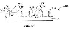
- first layer 4may be removed from regions 410 using a selective dry or wet etching process, leaving only the spacers 28 formed of hardmask layer 6 on substrate 2 as subresolution hardmask elements.
- the material of the remaining portion of third layer 34is resistant to the etchant used to remove first layer 4 . Therefore, third layer 34 protects underlying first layer 4 and second layer 8 in regions 420 from being removed, leaving a much larger hardmask element extending between spacers 28 bridged by the material of third layer 34 .
- substrate 2may be etched to form wells or apertures (shown by the dashed lines) having a controlled and accurate profile due to the symmetric profile of spacers 28 formed of hardmask layer 6 .
- the etch rate of the material of substrate 2 on each side of spacers 28is substantially the same.
- Etched structural features in substrate 2 using hardmask elements of the present inventionmay have aspect ratios of up to 5:1 or greater.
- hardmask featuresIn regions 420 where third layer 34 remains, bridging spacers 28 formed on the sides of third layer 34 , second layer 8 and first layer 4 , hardmask features have a slightly greater dimension than the original photopatterned and etched regions 410 prior to formation of hardmask layer 6 thereover, which dimension may be compensated for by slightly undersizing regions 410 to be used as regions 420 .
- the present inventionmay be used to facilitate simultaneous formation of both conventionally dimensioned and subresolution-dimensioned features in substrate 2 .
Landscapes
- Engineering & Computer Science (AREA)
- Microelectronics & Electronic Packaging (AREA)
- Condensed Matter Physics & Semiconductors (AREA)
- General Physics & Mathematics (AREA)
- Manufacturing & Machinery (AREA)
- Computer Hardware Design (AREA)
- Physics & Mathematics (AREA)
- Power Engineering (AREA)
- Chemical & Material Sciences (AREA)
- Inorganic Chemistry (AREA)
- Exposure And Positioning Against Photoresist Photosensitive Materials (AREA)
- Semiconductor Memories (AREA)
- Preparing Plates And Mask In Photomechanical Process (AREA)
Abstract
Description
- 1. Field of the Invention
- The present invention relates to the fabrication of integrated circuits. More specifically, the present invention relates to a method of producing fine geometry hardmasks with a controlled profile and height to enable the fabrication of precise subresolution features for integrated circuits and other structures.
- 2. State of the Art
- In fabrication of semiconductor devices including integrated circuitry, such as memory dice, conventional photolithography limits the ability to produce very fine structural features. Currently, photolithography is only capable of producing structural features of about 100 nm in minimum dimension. This inadequacy limits the ability of a manufacturer to produce extremely small structural features for integrated circuits through conventional photolithography processes. A capability to further reduce the dimensions of structural feature size is particularly important to the fabrication of semiconductor memory devices to enable increasing the number of memory cells on such semiconductor memory devices of a given size.
- U.S. Pat. No. 6,514,849 to Hui et al., U.S. Pat. No. 6,537,866 to Shields et al., U.S. Pat. No. 6,455,433 to Chang et al., U.S. Pat. No. 6,110,837 to Linliu et al., U.S. Pat. No. 5,916,821 to Kerber, U.S. Pat. No. 5,776,836 to Sandhu, and U.S. Pat. No. 5,296,410 to Yang attempt to overcome some of the problems associated with conventional photolithography.
- An alternative to using conventional photolithography is a technique called “loose photo patterning.” Generally described, loose photo patterning allows creating smaller mask features than would be possible with conventional photolithography. In loose photo patterning, mask features of conventional size are formed using conventional photolithography and dry etching, followed by coating such features with a layer of material. The layer of material is then removed from the top of the mask feature and the mask feature is subsequently etched away. These side coatings can be used as a hardmask to form so-called “subresolution” structural features, indicating that such structural features are of smaller dimensions than are achievable by using photolithography to form them directly. In other words, such features are smaller than the finest resolution photolithography processes can produce. Furthermore, all subresolution features will be the thickness of the coating used to coat the standard mask feature. Loose photo patterning allows creating mask features as small as 10 nm, which would not be possible with conventional photolithography.
- A method of forming features using conventional loose photo patterning will be better understood with reference to
FIGS. 1A-1D .FIG. 1A showsportion 100 ofsubstrate 2, such as p or n type silicon or other semiconductor substrate material, including afirst layer 4 deposited onsubstrate 2.First layer 4 is typically a silicon nitride layer approximately 900 Å in thickness.First layer 4 is formed into a selected geometry, as shown inFIG. 1A , using conventional photolithography and anisotropic etch processing. Referring toFIG. 1B , ahardmask layer 6 of, for example, 300 Å thick tetraethyloxysilicate (TEOS) silicon dioxide is deposited onfirst layer 4. As shown inFIG. 1C ,hardmask layer 6 is anisotropically etched to leave only the portion ofhardmask layer 6 covering the sidewalls offirst layer 4.First layer 4 is then completely removed fromsubstrate 2 by a dry or wet etch to form the sidewall spacer hardmask shown inFIG. 1D usable for further etching ofsubstrate 2 to define selected structural feature patterns therein. - While conventional loose photo patterning allows for forming fine geometry hardmask features, it also results in a phenomenon known as “sputtering.” As shown in
FIG. 1D , sputtering occurs whenhardmask layer 6 exhibits an asymmetric profile, which results in a poorly defined profile in the etched features ofunderlying substrate 2. These asymmetries ofhardmask layer 6 produce different etch rates adjacent the inner and outer edges ofhardmask layer 6 when theunderlying substrate 2 is etched. As the aspect (height or depth to width) ratios of etched features insubstrate 2 increase, the phenomenon of sputtering is aggravated and it becomes more important for the profile ofhardmask layer 6 to be symmetric and, preferably, rectangular. - Therefore, due to the limits of conventional photolithography and loose photo patterning it is desirable to develop a method which results in hardmask elements with an accurately controlled profile and height, enabling the semiconductor device fabricator to achieve an accurately etched profile in a substrate underlying the hardmask.
- The present invention, in a number of embodiments, includes methods for forming accurate, symmetric cross-section hardmask elements on an underlying substrate to enable the fabrication by etching of precise structural features in the substrate and resulting end products incorporating such features. The resulting hardmask elements may be used to accurately etch well-defined, high aspect ratio features in the substrate free of sputtering defects.
- In one exemplary embodiment, a method for forming hardmasks on a substrate is provided. First, a substrate is provided. Next, a first layer of a material may be formed on the substrate. Following formation of the first layer, a second layer may be formed on the exposed surface of the first layer. Next, a plurality of discrete structures may be formed on the substrate by masking, patterning and etching the first and second layers to a geometry defined by an exposed surface of the second layer and substantially vertical sidewalls extending upward from the substrate to the exposed surface. Following formation of the plurality of structures, a hardmask layer made may be deposited over the substrate and the plurality of discrete structures. Portions of the hardmask layer adhered to the exposed surface of the second layer may then be removed by an etching process, which also removes the portions of the hardmask layer on the substrate between the discrete structures, while the portions of the hardmask layer flanking the discrete structures remain as spacers, exhibiting an asymmetric profile. The discrete structures may then be planarized by an abrasive process such as chemical mechanical planarization (CMP) to remove the entire second layer and the laterally adjacent, uppermost, asymmetric ends of the remaining hardmask portion spacers. Following planarization, the first layer may be removed by a selective etching process, leaving only the remaining spacers formed as portions of the sidewalls of the original hardmask layer, providing well-defined, symmetrical hardmask elements for etching of the underlying substrate. The method of the above exemplary embodiment produces hardmask features having a well-defined, symmetric cross-section.
- In another exemplary embodiment, a method for forming hardmask elements of various sizes on a substrate is disclosed. First, a substrate is provided. A first layer of a material may then be formed on the substrate. Following formation of the first layer, a second layer may be deposited on the exposed surface of the first layer. A plurality of discrete structures may then be formed by masking, patterning and etching the first and second layers to a geometry defined by an exposed surface of the second layer and substantially vertical sidewalls extending from the substrate to the exposed surface. Following formation of the plurality of structures, a hardmask layer may be deposited over the substrate and the plurality of discrete structures. The portion of the hardmask layer adhered to the exposed surface of the second layer may then be removed by an etching process, which also removes the portions of the hardmask layer between the discrete structures, while portions of the hardmask layer flanking the structures remain as spacers which exhibit an asymmetric profile. The discrete structures may then be planarized by an abrasive process such as CMP to remove the entire second layer and the laterally adjacent, uppermost ends of the remaining hardmask portion spacers. Following planarization, the exposed upper surface of the first layer of material of at least one of the structures may be protected and the unprotected portions of the first layer of the structures removed by an etching process. The method of the above exemplary embodiment produces hardmask features of various sizes having a well-defined, symmetric cross-section.
- In yet another exemplary embodiment, a method for forming hardmasks of various sizes on a substrate is disclosed. A substrate is provided and a first layer of a material may be formed on the substrate. Following formation of the first layer, a second layer may be deposited on the exposed surface of the first layer. After formation of the second layer, a third layer of a material may be formed on the exposed surface of the second layer. A plurality of discrete structures may then be formed by masking, patterning and etching the first layer, the second layer, and the third layer to a geometry defined by an exposed surface of the third layer and substantially vertical sidewalls extending from the substrate to the exposed surface. After formation of the plurality of discrete structures, the exposed upper surface of at least one of the plurality of discrete structures may be protected. A hardmask layer may be deposited over the substrate and the plurality of discrete structures. Following deposition of the hardmask layer, the portions of the hardmask layer on the substrate and on the upper surfaces of the discrete structures may be removed by an etching process, the etching also removing the third layer and a portion of the second layer on any unprotected discrete structure. The plurality of discrete structures may be planarized to remove the second layer, the planarization stopping on the first layer of the unprotected discrete structures and the third layer of the at least one protected discrete structure. Finally, the exposed portions of the first layer may be removed by an etching process. The method of the above exemplary embodiment produces hardmask features of various sizes having a well-defined, symmetric cross-section.
- These features, advantages, and alternative aspects of the present invention will be apparent to those skilled in the art from a consideration of the following detailed description taken in combination with the accompanying drawings.
- In the drawings, which illustrate what is currently considered to be the best mode for carrying out the invention:
FIGS. 1A-1D are schematic sectional views illustrating a conventional loose photo patterning process.FIGS. 2A-2I are schematic sectional views illustrating an exemplary embodiment of a method of the present invention.FIGS. 3A-3D are schematic sectional views illustrating another exemplary embodiment of a method of the present invention.FIGS. 4A-4K are schematic sectional views illustrating yet another exemplary embodiment of a method of the present invention.- In the description which follows, like features and elements in the several embodiments are identified with the same or similar reference numerals for the convenience of the reader.
FIGS. 2A-2I illustrate an exemplary embodiment of a method of the present invention suitable for producing hardmask elements having an accurate, symmetric, rectangular cross-section. Referring toFIG. 2A ,substrate 2 is provided made from a suitable semiconductor substrate such as silicon, polysilicon, or a layered semiconductor structure such as a silicon on insulator (SOI) structure, as exemplified by silicon on glass (SOG) and silicon on sapphire (SOS) structures.Substrate 2 may also be a glass material useful for forming reticles, such as soda-lime glass, borosilicate glass, or quartz. Then, as shown inFIG. 2B , afirst layer 4 havingupper surface 16 may be formed on and adhered toportion 200 ofsubstrate 2 using techniques such as, for example, chemical vapor deposition (CVD), physical vapor deposition (PVD), or atomic layer deposition (ALD).First layer 4 may be formed from materials such as silicon nitride. In this exemplary embodiment,first layer 4 may be formed from 500 Å thick silicon nitride.- Referring to
FIG. 2C , following deposition offirst layer 4,second layer 8 may be deposited on top of and adhered to theupper surface 16 offirst layer 4.Second layer 8 may be formed from TEOS-type silicon dioxide.Second layer 8 may be deposited using techniques such as, for example, CVD, PVD, or ALD. In this exemplary embodiment,second layer 8 may be formed from 500 Å thick TEOS-type silicon dioxide. - Referring to
FIG. 2D , following deposition ofsecond layer 8,portion 200 may be covered with a patterned and developedphotoresist 12, etched, and discrete structures in the form ofregions 210 formed from etched first andsecond layers FIG. 2E ,regions 210 are shown after etching and subsequent removal ofphotoresist 12. As shown inFIG. 2E ,regions 210 formed of the remaining segments offirst layer 4 andsecond layer 8 may exhibit a geometry defined by substantiallyvertical sidewalls 24 extending fromsubstrate 2 to exposedupper surface 26 ofsecond layer 8. - Referring to
FIG. 2F , following forming ofregions 210,hardmask layer 6 may be formed overregions 210 and exposed portions ofsubstrate 2 betweenregions 210.Hardmask layer 6 adheres toregions 210 and intervening portions ofsubstrate 2.Hardmask layer 6 may be formed from materials such as TEOS-type silicon dioxide, silicon nitride, polysilicon, titanium nitride, aluminum oxide (Al2O3), amorphous carbon, or other suitable material, depending on the material ofsubstrate 2,first layer 4,second layer 8, and the intended etch chemistry to be used withhardmask layer 6. In an exemplary embodiment,hardmask layer 6 may be formed from 300 Å thick TEOS-type silicon dioxide.Hardmask layer 6 may be deposited by a process useful for precisely defining a thickness thereof such as, for example, low pressure chemical vapor deposition (LPCVD) or atomic layer deposition (ALD). - Referring to
FIG. 2G , following deposition ofhardmask layer 6,hardmask layer 6 andsecond layer 8 may be anisotropically etched to leave only portions ofhardmask layer 6 covering the sides ofregions 210 comprised of the remaining portions offirst layer 4 andsecond layer 8 to formspacers 28. In other words, the portion ofhardmask layer 6 adhered to theupper surface 26 ofsecond layer 8 may be removed by etching, which also removes the portions ofhardmask layer 6 onsubstrate 2 betweenregions 210.Second layer 8 may not be completely etched through as is shown inFIG. 2G , leaving a sufficient thickness ofsecond layer 8 remaining to allowspacer 28 to be of stable (constant) thickness at a height at least coincident with the top offirst layer 4. - Referring to
FIG. 2H , following etching ofhardmask layer 6, upper portions ofspacers 28 formed fromhardmask layer 6 and all ofsecond layer 8 may be removed by an abrasive planarization process such as CMP. A CMP compound may be selected for the polishing slurry that will not removefirst layer 4, instead stopping onupper surface 16 thereof. In an exemplary embodiment, spacers28 may be about 2000 Å in height. The remainingspacers 28 formed ofhardmask layer 6 exhibit a symmetric, rectangular cross-section. - Referring to
FIG. 2I ,first layer 4 may then be removed using a selective dry or wet etching process, leaving only thespacers 28 formed ofhardmask layer 6 onsubstrate 2 as hardmask elements. Subsequently,substrate 2 may be etched to form wells (shown by the dashed lines) or apertures having a controlled and accurate profile free from sputtering defects using the hardmaskelements comprising spacers 28 formed ofhardmask layer 6 as an etch mask. Due to the symmetrical cross-section ofspacers 28 and the rectangular, squared-off upper portion of the cross-section, the etch rate on each side ofspacers 28 is substantially the same, eliminating asymmetry in the pattern etched intosubstrate 2. Etched features insubstrate 2 using hardmasks of the present invention may have aspect ratios of up to 5:1 or more. - In another exemplary embodiment of a method of the present invention, hardmask spacers of a symmetric geometry may be formed to various widths according to the design of the desired structural features to be etched in
substrate 2. Referring toFIG. 3A , a plurality of discrete structures in the form ofregions 210 may be formed onsubstrate 2.Regions 210 shown inFIG. 3A includefirst layer 4 as previously described, bounded byspacers 28 made fromhardmask layer 6.Regions 210 shown inFIG. 3A may be formed as in the previous exemplary embodiment as shown and described with respect toFIGS. 2A-2H . Referring toFIG. 3B , aphotoresist 30 may be applied toupper surface 32 offirst layer 4 and selectively patterned and developed using conventional photolithography techniques to coverupper surfaces 32 of at least oneregion 210. - Referring to
FIG. 3C , following application of resist30,first layer 4 may be removed fromregions 210 that are not protected withphotoresist 30 using an appropriate selective dry or wet etching process. Next,photoresist 30 may then be removed using conventional techniques. Thus, subresolution hardmask elements are formed ofspacers 28 wherefirst layer 4 has been removed, while larger, conventionally dimensioned hardmask elements are formed from theregions 210 wherefirst layer 4 remains flanked byspacers 28, the larger hardmask elements being of only slightly larger dimension than that of eachregion 210 prior to deposition ofhardmask layer 6. By intentionally undersizing a givenregion 210 intended to form a larger hardmask element to allow for the added width provided byspacers 28, the dimensions of larger hardmask elements may be precisely controlled. Subsequently,substrate 2 may be etched to form wells or apertures W of various widths (shown by the broken lines) and having a controlled and accurate profile due to the symmetric profile of thespacers 28 formed ofhardmask layer 6. Thus, both conventionally dimensioned features as well as subresolution-sized features may be formed. Alternatively, by using an etchant suitable for removal of the material oflayer 4 as well assubstrate 2, wells or apertures W1and W2of different depths may be formed, as depicted inFIG. 3D . As in the previous exemplary embodiment, due to the precise, squared-off cross-section ofspacers 28, the etch rate on each side ofspacers 28 as well as ofregions 210 having flankingspacers 28 is substantially the same. Etched features insubstrate 2 using hardmasks of the present invention may have aspect ratios of up to 5:1 or greater. FIGS. 4A-4K illustrate yet another exemplary embodiment of a method of the present invention suitable for producing hardmask spacers of various widths yet having an accurate, symmetric, rectangular geometry. Referring toFIG. 4A ,substrate 2 is provided of a suitable semiconductor substrate such as silicon, polysilicon, or a layered semiconductor structure such as a silicon on insulator (SOD) structure, as exemplified by silicon on glass (SOG) and silicon on sapphire (SOS) structures.Substrate 2 may also be a glass useful for forming reticles such as soda-lime glass, borosilicate glass, or quartz. Then, as shown inFIG. 4B , afirst layer 4 havingupper surface 16 may be formed on and adhered toportion 400 ofsubstrate 2 using techniques such as CVD, PVD, or ALD.First layer 4 may be formed from materials such as silicon nitride or other suitable material as noted above. In an exemplary embodiment,first layer 4 may be formed from 500 Å thick silicon nitride.- Referring to
FIG. 4C , following formation offirst layer 4,second layer 8 may be deposited on top of and adhered to theupper surface 16 offirst layer 4.Second layer 8 may be formed from TEOS-type silicon dioxide or other suitable material as noted above.Second layer 8 may be deposited using techniques such as CVD, PVD, or ALD. In an exemplary embodiment,second layer 8 may be formed from 500 Å thick TEOS-type silicon dioxide. Next, referring toFIG. 4D ,third layer 34 havingupper surface 37 may be formed from aluminum oxide (Al2O3). In an exemplary embodiment,third layer 34 may be formed from 100 Å thick Al2O3. - Referring to
FIG. 4E , following deposition ofthird layer 34,portion 400 may be covered by a patterned and developedphotoresist 36 and anisotropically etched using conventional techniques known to those of ordinary skill in the art to form discrete structures in the form ofregions 410. Referring toFIG. 4F ,regions 410 are shown after etching and removal ofphotoresist 36. As shown inFIG. 4F ,regions 410 may exhibit a geometry defined by substantiallyvertical sidewalls 42 extending fromsubstrate 2 toupper surfaces 40. - Referring to
FIG. 4G , following formation ofregions 410,photoresist 38 may be selectively patterned over theupper surface 40 of one ormore regions 410. Theregions 410 covered and protected byphotoresist 38 will be referred to asregions 420. - Referring to
FIG. 4H ,hardmask layer 6 may be formed oversubstrate 2,regions 410 formed offirst layer 4,second layer 8,third layer 34 and, wherephotoresist 38 is present,regions 420.Hardmask layer 6 covers portions ofsubstrate 2 betweenregions Hardmask layer 6 adheres tofirst layer 4,second layer 8,third layer 34,photoresist 38 and intervening portions ofsubstrate 2.Hardmask layer 6 may be formed from materials such as TEOS-type silicon dioxide, silicon nitride, polysilicon, titanium nitride, amorphous carbon, or aluminum oxide (Al2O3) depending on the material ofsubstrate 2,first layer 4,second layer 8,third layer 34, and the intended etch chemistry to be used withhardmask layer 6. In an exemplary embodiment,hardmask layer 6 may be formed from 300 Å thick TEOS-type silicon dioxide.Hardmask layer 6 may be deposited by a process such as low pressure chemical vapor deposition (LPCVD) or atomic layer deposition (ALD). - Referring to
FIG. 4I , following deposition ofhardmask layer 6,hardmask layer 6,third layer 34 and a portion ofsecond layer 8 may be anisotropically etched inregions 410 where resist38 is not present, leaving only portions ofhardmask layer 6 formingspacers 28 covering the sides offirst layer 4 andsecond layer 8. In theregions 410 wheresecond layer 8 is etched, it is not completely etched. Instead, a sufficient thickness ofsecond layer 8 remains after this etching step to ensurespacers 28 are at a stable (constant) thickness at least to a level coincident with the top offirst layer 4. Furthermore, in theregions 420 wherethird layer 34 is protected byphotoresist 38, it is not completely removed. Instead, the remaining portion ofthird layer 34 may be typically about 80 Å thick following etching. - Referring to
FIG. 4J , following etching ofhardmask layer 6,regions 410 andregions 420 may be planarized using an abrasive process such as CMP. Whileregions 420 are slightly higher thanregions 410, the CMP process is capable of simultaneously planarizing both regions due to the CMP pad being formed of a yieldable or deformable material. A CMP compound for a slurry may be selected that will stop onfirst layer 4 inregions 410 and stop on the remaining thickness ofthird layer 34 inregions 420. The remaining sidewall portions ofhardmask layer 6 formingspacers 28 exhibit a symmetric, rectangular profile. - Referring to
FIG. 4K , after CMP,first layer 4 may be removed fromregions 410 using a selective dry or wet etching process, leaving only thespacers 28 formed ofhardmask layer 6 onsubstrate 2 as subresolution hardmask elements. The material of the remaining portion ofthird layer 34 is resistant to the etchant used to removefirst layer 4. Therefore,third layer 34 protects underlyingfirst layer 4 andsecond layer 8 inregions 420 from being removed, leaving a much larger hardmask element extending betweenspacers 28 bridged by the material ofthird layer 34. Subsequently,substrate 2 may be etched to form wells or apertures (shown by the dashed lines) having a controlled and accurate profile due to the symmetric profile ofspacers 28 formed ofhardmask layer 6. The etch rate of the material ofsubstrate 2 on each side ofspacers 28 is substantially the same. Etched structural features insubstrate 2 using hardmask elements of the present invention may have aspect ratios of up to 5:1 or greater. Inregions 420 wherethird layer 34 remains, bridgingspacers 28 formed on the sides ofthird layer 34,second layer 8 andfirst layer 4, hardmask features have a slightly greater dimension than the original photopatterned and etchedregions 410 prior to formation ofhardmask layer 6 thereover, which dimension may be compensated for by slightly undersizingregions 410 to be used asregions 420. As a result, the present invention may be used to facilitate simultaneous formation of both conventionally dimensioned and subresolution-dimensioned features insubstrate 2. - Although the foregoing description contains many specifics, these are not to be construed as limiting the scope of the present invention, but merely as providing certain exemplary embodiments. Similarly, other embodiments of the invention may be devised which do not depart from the spirit or scope of the present invention. The scope of the invention is, therefore, indicated and limited only by the appended claims and their legal equivalents, rather than by the foregoing description. All additions, deletions, and modifications to the invention, as disclosed herein, which fall within the meaning and scope of the claims are encompassed by the present invention.
Claims (54)
Priority Applications (2)
| Application Number | Priority Date | Filing Date | Title |
|---|---|---|---|
| US10/883,215US7473644B2 (en) | 2004-07-01 | 2004-07-01 | Method for forming controlled geometry hardmasks including subresolution elements |
| US11/523,331US20070020939A1 (en) | 2004-07-01 | 2006-09-19 | Controlled geometry hardmask including subresolution elements |
Applications Claiming Priority (1)
| Application Number | Priority Date | Filing Date | Title |
|---|---|---|---|
| US10/883,215US7473644B2 (en) | 2004-07-01 | 2004-07-01 | Method for forming controlled geometry hardmasks including subresolution elements |
Related Child Applications (1)
| Application Number | Title | Priority Date | Filing Date |
|---|---|---|---|
| US11/523,331DivisionUS20070020939A1 (en) | 2004-07-01 | 2006-09-19 | Controlled geometry hardmask including subresolution elements |
Publications (2)
| Publication Number | Publication Date |
|---|---|
| US20060003182A1true US20060003182A1 (en) | 2006-01-05 |
| US7473644B2 US7473644B2 (en) | 2009-01-06 |
Family
ID=35514312
Family Applications (2)
| Application Number | Title | Priority Date | Filing Date |
|---|---|---|---|
| US10/883,215Active2025-10-23US7473644B2 (en) | 2004-07-01 | 2004-07-01 | Method for forming controlled geometry hardmasks including subresolution elements |
| US11/523,331AbandonedUS20070020939A1 (en) | 2004-07-01 | 2006-09-19 | Controlled geometry hardmask including subresolution elements |
Family Applications After (1)
| Application Number | Title | Priority Date | Filing Date |
|---|---|---|---|
| US11/523,331AbandonedUS20070020939A1 (en) | 2004-07-01 | 2006-09-19 | Controlled geometry hardmask including subresolution elements |
Country Status (1)
| Country | Link |
|---|---|
| US (2) | US7473644B2 (en) |
Cited By (45)
| Publication number | Priority date | Publication date | Assignee | Title |
|---|---|---|---|---|
| US20060264001A1 (en)* | 2004-08-31 | 2006-11-23 | Luan Tran | Structures with increased photo-alignment margins |
| US20070050748A1 (en)* | 2005-08-30 | 2007-03-01 | Micron Technology, Inc., A Corporation | Method and algorithm for random half pitched interconnect layout with constant spacing |
| US20070045712A1 (en)* | 2005-09-01 | 2007-03-01 | Haller Gordon A | Memory cell layout and process flow |
| US20070049035A1 (en)* | 2005-08-31 | 2007-03-01 | Tran Luan C | Method of forming pitch multipled contacts |
| US20070105357A1 (en)* | 2005-09-01 | 2007-05-10 | Micron Technology, Inc. | Silicided recessed silicon |
| US20070148984A1 (en)* | 2004-09-02 | 2007-06-28 | Micron Technology, Inc. | Method for integrated circuit fabrication using pitch multiplication |
| US20070238308A1 (en)* | 2006-04-07 | 2007-10-11 | Ardavan Niroomand | Simplified pitch doubling process flow |
| US20070249170A1 (en)* | 2006-04-25 | 2007-10-25 | David Kewley | Process for improving critical dimension uniformity of integrated circuit arrays |
| US20070281219A1 (en)* | 2006-06-01 | 2007-12-06 | Sandhu Gurtej S | Masking techniques and contact imprint reticles for dense semiconductor fabrication |
| US20080058852A1 (en)* | 2006-09-01 | 2008-03-06 | Ihde Glenn M | Fluid Absorbent Surgical Device for Trocars |
| US20080149593A1 (en)* | 2005-08-25 | 2008-06-26 | Micron Technology, Inc. | Multiple deposition for integration of spacers in pitch multiplication process |
| WO2008033695A3 (en)* | 2006-09-14 | 2008-08-07 | Micron Technology Inc | Efficient pitch multiplication process |
| US20080227293A1 (en)* | 2005-03-28 | 2008-09-18 | Micron Technology, Inc. | Integrated circuit fabrication |
| US20080254627A1 (en)* | 2005-06-09 | 2008-10-16 | Micron Technology, Inc. | Method for adjusting feature size and position |
| US20080261349A1 (en)* | 2005-09-01 | 2008-10-23 | Micron Technology, Inc. | Protective coating for planarization |
| US20080290374A1 (en)* | 2005-07-29 | 2008-11-27 | Micron Technology, Inc. | Layout for high density conductive interconnects |
| US20080299753A1 (en)* | 2005-09-01 | 2008-12-04 | Figura Thomas A | Peripheral Gate Stacks and Recessed Array Gates |
| US20080299774A1 (en)* | 2007-06-04 | 2008-12-04 | Micron Technology, Inc. | Pitch multiplication using self-assembling materials |
| US20090152645A1 (en)* | 2007-12-18 | 2009-06-18 | Micron Technology, Inc. | Methods for isolating portions of a loop of pitch-multiplied material and related structures |
| US7560390B2 (en) | 2005-06-02 | 2009-07-14 | Micron Technology, Inc. | Multiple spacer steps for pitch multiplication |
| US7572572B2 (en) | 2005-09-01 | 2009-08-11 | Micron Technology, Inc. | Methods for forming arrays of small, closely spaced features |
| US7611980B2 (en) | 2006-08-30 | 2009-11-03 | Micron Technology, Inc. | Single spacer process for multiplying pitch by a factor greater than two and related intermediate IC structures |
| US7651951B2 (en) | 2005-03-15 | 2010-01-26 | Micron Technology, Inc. | Pitch reduced patterns relative to photolithography features |
| US7655387B2 (en) | 2004-09-02 | 2010-02-02 | Micron Technology, Inc. | Method to align mask patterns |
| US7659208B2 (en) | 2007-12-06 | 2010-02-09 | Micron Technology, Inc | Method for forming high density patterns |
| US20100062579A1 (en)* | 2008-09-11 | 2010-03-11 | Micron Technology, Inc. | Self-aligned trench formation |
| US20100130016A1 (en)* | 2008-11-24 | 2010-05-27 | Micron Technology, Inc. | Methods of forming a masking pattern for integrated circuits |
| US7737039B2 (en) | 2007-11-01 | 2010-06-15 | Micron Technology, Inc. | Spacer process for on pitch contacts and related structures |
| US7759197B2 (en) | 2005-09-01 | 2010-07-20 | Micron Technology, Inc. | Method of forming isolated features using pitch multiplication |
| US7776744B2 (en) | 2005-09-01 | 2010-08-17 | Micron Technology, Inc. | Pitch multiplication spacers and methods of forming the same |
| US7842558B2 (en) | 2006-03-02 | 2010-11-30 | Micron Technology, Inc. | Masking process for simultaneously patterning separate regions |
| US7884022B2 (en) | 2005-03-15 | 2011-02-08 | Round Rock Research, Llc | Multiple deposition for integration of spacers in pitch multiplication process |
| US7910288B2 (en) | 2004-09-01 | 2011-03-22 | Micron Technology, Inc. | Mask material conversion |
| US7919414B2 (en) | 2007-06-26 | 2011-04-05 | Hynix Semiconductor Inc. | Method for forming fine patterns in semiconductor device |
| US8003310B2 (en) | 2006-04-24 | 2011-08-23 | Micron Technology, Inc. | Masking techniques and templates for dense semiconductor fabrication |
| US20110230853A1 (en)* | 2006-09-01 | 2011-09-22 | Ihde Ii Glenn M | Fluid Absorbent Surgical Device for Trocars |
| US8030218B2 (en) | 2008-03-21 | 2011-10-04 | Micron Technology, Inc. | Method for selectively modifying spacing between pitch multiplied structures |
| US8076208B2 (en) | 2008-07-03 | 2011-12-13 | Micron Technology, Inc. | Method for forming transistor with high breakdown voltage using pitch multiplication technique |
| US8114573B2 (en) | 2006-06-02 | 2012-02-14 | Micron Technology, Inc. | Topography based patterning |
| US8207614B2 (en) | 2005-05-23 | 2012-06-26 | Micron Technology, Inc. | Methods for forming arrays of small, closely spaced features |
| US20130203266A1 (en)* | 2012-02-02 | 2013-08-08 | Globalfoundries Inc. | Methods of Forming Metal Nitride Materials |
| US8563229B2 (en) | 2007-07-31 | 2013-10-22 | Micron Technology, Inc. | Process of semiconductor fabrication with mask overlay on pitch multiplied features and associated structures |
| US20150214062A1 (en)* | 2014-01-30 | 2015-07-30 | Anirban Roy | Methods For Extending Floating Gates For NVM Cells To Form Sub-Lithographic Features And Related NVM Cells |
| US9603753B2 (en) | 2014-07-16 | 2017-03-28 | II Glenn M. Ihde | Fluid absorbent surgical device for cannulas |
| US11348788B2 (en)* | 2007-07-30 | 2022-05-31 | Micron Technology, Inc. | Methods for device fabrication using pitch reduction |
Families Citing this family (4)
| Publication number | Priority date | Publication date | Assignee | Title |
|---|---|---|---|---|
| US7476933B2 (en) | 2006-03-02 | 2009-01-13 | Micron Technology, Inc. | Vertical gated access transistor |
| US8969213B2 (en) | 2012-07-30 | 2015-03-03 | International Business Machines Corporation | Non-lithographic line pattern formation |
| US9698015B2 (en)* | 2013-10-21 | 2017-07-04 | Applied Materials, Inc. | Method for patterning a semiconductor substrate |
| US10838298B2 (en) | 2016-09-21 | 2020-11-17 | Molecular Imprints, Inc. | Microlithographic fabrication of structures |
Citations (26)
| Publication number | Priority date | Publication date | Assignee | Title |
|---|---|---|---|---|
| US3736534A (en)* | 1971-10-13 | 1973-05-29 | Litton Systems Inc | Planar-shielded meander slow-wave structure |
| US4791046A (en)* | 1984-04-26 | 1988-12-13 | Oki Electric Industry Co., Ltd. | Process for forming mask patterns of positive type resist material with trimethylsilynitrile |
| US5296410A (en)* | 1992-12-16 | 1994-03-22 | Samsung Electronics Co., Ltd. | Method for separating fine patterns of a semiconductor device |
| US5618383A (en)* | 1994-03-30 | 1997-04-08 | Texas Instruments Incorporated | Narrow lateral dimensioned microelectronic structures and method of forming the same |
| US5776836A (en)* | 1996-02-29 | 1998-07-07 | Micron Technology, Inc. | Self aligned method to define features smaller than the resolution limit of a photolithography system |
| US5916821A (en)* | 1995-07-17 | 1999-06-29 | Siemens Aktiengesellschaft | Method for producing sublithographic etching masks |
| US6110837A (en)* | 1999-04-28 | 2000-08-29 | Worldwide Semiconductor Manufacturing Corp. | Method for forming a hard mask of half critical dimension |
| US6399286B1 (en)* | 1999-06-23 | 2002-06-04 | Taiwan Semiconductor Manufacturing Corp. | Method of fabricating reduced critical dimension for conductive line and space |
| US20020074309A1 (en)* | 1998-02-11 | 2002-06-20 | Applied Materials, Inc. | Integrated low k dielectrics and etch stops |
| US6455433B1 (en)* | 2001-03-30 | 2002-09-24 | Taiwan Semiconductor Manufacturing Co., Ltd. | Method for forming square-shouldered sidewall spacers and devices fabricated |
| US20020137344A1 (en)* | 2000-07-26 | 2002-09-26 | Jordan Stephen G. | Etched substrate |
| US6492212B1 (en)* | 2001-10-05 | 2002-12-10 | International Business Machines Corporation | Variable threshold voltage double gated transistors and method of fabrication |
| US6514849B1 (en)* | 2001-04-02 | 2003-02-04 | Advanced Micro Devices, Inc. | Method of forming smaller contact size using a spacer hard mask |
| US6537866B1 (en)* | 2000-10-18 | 2003-03-25 | Advanced Micro Devices, Inc. | Method of forming narrow insulating spacers for use in reducing minimum component size |
| US6610607B1 (en)* | 2000-05-25 | 2003-08-26 | International Business Machines Corporation | Method to define and tailor process limited lithographic features using a modified hard mask process |
| US6617098B1 (en)* | 1999-07-13 | 2003-09-09 | Input/Output, Inc. | Merged-mask micro-machining process |
| US20030224559A1 (en)* | 2002-05-28 | 2003-12-04 | Applied Materials, Inc. | Micromachined structures including glass vias with internal conductive layers anodically bonded to silicon-containing substrates |
| US6664173B2 (en)* | 2002-01-09 | 2003-12-16 | Intel Corporation | Hardmask gate patterning technique for all transistors using spacer gate approach for critical dimension control |
| US6858542B2 (en)* | 2003-01-17 | 2005-02-22 | Freescale Semiconductor, Inc. | Semiconductor fabrication method for making small features |
| US6867116B1 (en)* | 2003-11-10 | 2005-03-15 | Macronix International Co., Ltd. | Fabrication method of sub-resolution pitch for integrated circuits |
| US20050087809A1 (en)* | 2003-10-28 | 2005-04-28 | International Business Machines Corporation | Nanocircuit and self-correcting etching method for fabricating same |
| US20050127432A1 (en)* | 2003-12-03 | 2005-06-16 | Taiwan Semiconductor Manufacturing Co., Ltd. | Semiconductor device having substantially planar contacts and body |
| US20050136663A1 (en)* | 2003-12-19 | 2005-06-23 | Agency For Science, Technology And Research | Single-crystal-silicon 3D micromirror |
| US6924191B2 (en)* | 2002-06-20 | 2005-08-02 | Applied Materials, Inc. | Method for fabricating a gate structure of a field effect transistor |
| US7078160B2 (en)* | 2003-06-26 | 2006-07-18 | Intel Corporation | Selective surface exposure, cleans, and conditioning of the germanium film in a Ge photodetector |
| US20070037395A1 (en)* | 2005-08-10 | 2007-02-15 | Milton Beachy | Stringer elimination in a BiCMOS process |
Family Cites Families (1)
| Publication number | Priority date | Publication date | Assignee | Title |
|---|---|---|---|---|
| US6649426B2 (en) | 2001-06-28 | 2003-11-18 | Advanced Micro Devices, Inc. | System and method for active control of spacer deposition |
- 2004
- 2004-07-01USUS10/883,215patent/US7473644B2/enactiveActive
- 2006
- 2006-09-19USUS11/523,331patent/US20070020939A1/ennot_activeAbandoned
Patent Citations (26)
| Publication number | Priority date | Publication date | Assignee | Title |
|---|---|---|---|---|
| US3736534A (en)* | 1971-10-13 | 1973-05-29 | Litton Systems Inc | Planar-shielded meander slow-wave structure |
| US4791046A (en)* | 1984-04-26 | 1988-12-13 | Oki Electric Industry Co., Ltd. | Process for forming mask patterns of positive type resist material with trimethylsilynitrile |
| US5296410A (en)* | 1992-12-16 | 1994-03-22 | Samsung Electronics Co., Ltd. | Method for separating fine patterns of a semiconductor device |
| US5618383A (en)* | 1994-03-30 | 1997-04-08 | Texas Instruments Incorporated | Narrow lateral dimensioned microelectronic structures and method of forming the same |
| US5916821A (en)* | 1995-07-17 | 1999-06-29 | Siemens Aktiengesellschaft | Method for producing sublithographic etching masks |
| US5776836A (en)* | 1996-02-29 | 1998-07-07 | Micron Technology, Inc. | Self aligned method to define features smaller than the resolution limit of a photolithography system |
| US20020074309A1 (en)* | 1998-02-11 | 2002-06-20 | Applied Materials, Inc. | Integrated low k dielectrics and etch stops |
| US6110837A (en)* | 1999-04-28 | 2000-08-29 | Worldwide Semiconductor Manufacturing Corp. | Method for forming a hard mask of half critical dimension |
| US6399286B1 (en)* | 1999-06-23 | 2002-06-04 | Taiwan Semiconductor Manufacturing Corp. | Method of fabricating reduced critical dimension for conductive line and space |
| US6617098B1 (en)* | 1999-07-13 | 2003-09-09 | Input/Output, Inc. | Merged-mask micro-machining process |
| US6610607B1 (en)* | 2000-05-25 | 2003-08-26 | International Business Machines Corporation | Method to define and tailor process limited lithographic features using a modified hard mask process |
| US20020137344A1 (en)* | 2000-07-26 | 2002-09-26 | Jordan Stephen G. | Etched substrate |
| US6537866B1 (en)* | 2000-10-18 | 2003-03-25 | Advanced Micro Devices, Inc. | Method of forming narrow insulating spacers for use in reducing minimum component size |
| US6455433B1 (en)* | 2001-03-30 | 2002-09-24 | Taiwan Semiconductor Manufacturing Co., Ltd. | Method for forming square-shouldered sidewall spacers and devices fabricated |
| US6514849B1 (en)* | 2001-04-02 | 2003-02-04 | Advanced Micro Devices, Inc. | Method of forming smaller contact size using a spacer hard mask |
| US6492212B1 (en)* | 2001-10-05 | 2002-12-10 | International Business Machines Corporation | Variable threshold voltage double gated transistors and method of fabrication |
| US6664173B2 (en)* | 2002-01-09 | 2003-12-16 | Intel Corporation | Hardmask gate patterning technique for all transistors using spacer gate approach for critical dimension control |
| US20030224559A1 (en)* | 2002-05-28 | 2003-12-04 | Applied Materials, Inc. | Micromachined structures including glass vias with internal conductive layers anodically bonded to silicon-containing substrates |
| US6924191B2 (en)* | 2002-06-20 | 2005-08-02 | Applied Materials, Inc. | Method for fabricating a gate structure of a field effect transistor |
| US6858542B2 (en)* | 2003-01-17 | 2005-02-22 | Freescale Semiconductor, Inc. | Semiconductor fabrication method for making small features |
| US7078160B2 (en)* | 2003-06-26 | 2006-07-18 | Intel Corporation | Selective surface exposure, cleans, and conditioning of the germanium film in a Ge photodetector |
| US20050087809A1 (en)* | 2003-10-28 | 2005-04-28 | International Business Machines Corporation | Nanocircuit and self-correcting etching method for fabricating same |
| US6867116B1 (en)* | 2003-11-10 | 2005-03-15 | Macronix International Co., Ltd. | Fabrication method of sub-resolution pitch for integrated circuits |
| US20050127432A1 (en)* | 2003-12-03 | 2005-06-16 | Taiwan Semiconductor Manufacturing Co., Ltd. | Semiconductor device having substantially planar contacts and body |
| US20050136663A1 (en)* | 2003-12-19 | 2005-06-23 | Agency For Science, Technology And Research | Single-crystal-silicon 3D micromirror |
| US20070037395A1 (en)* | 2005-08-10 | 2007-02-15 | Milton Beachy | Stringer elimination in a BiCMOS process |
Cited By (168)
| Publication number | Priority date | Publication date | Assignee | Title |
|---|---|---|---|---|
| US20060264001A1 (en)* | 2004-08-31 | 2006-11-23 | Luan Tran | Structures with increased photo-alignment margins |
| US8030222B2 (en) | 2004-08-31 | 2011-10-04 | Round Rock Research, Llc | Structures with increased photo-alignment margins |
| US8895232B2 (en) | 2004-09-01 | 2014-11-25 | Micron Technology, Inc. | Mask material conversion |
| US7910288B2 (en) | 2004-09-01 | 2011-03-22 | Micron Technology, Inc. | Mask material conversion |
| US8486610B2 (en) | 2004-09-01 | 2013-07-16 | Micron Technology, Inc. | Mask material conversion |
| US7629693B2 (en) | 2004-09-02 | 2009-12-08 | Micron Technology, Inc | Method for integrated circuit fabrication using pitch multiplication |
| US20100203727A1 (en)* | 2004-09-02 | 2010-08-12 | Micron Technology, Inc. | Method for integrated circuit fabrication using pitch multiplication |
| US20070148984A1 (en)* | 2004-09-02 | 2007-06-28 | Micron Technology, Inc. | Method for integrated circuit fabrication using pitch multiplication |
| US8674512B2 (en) | 2004-09-02 | 2014-03-18 | Micron Technology, Inc. | Method to align mask patterns |
| US7655387B2 (en) | 2004-09-02 | 2010-02-02 | Micron Technology, Inc. | Method to align mask patterns |
| US7687408B2 (en) | 2004-09-02 | 2010-03-30 | Micron Technology, Inc. | Method for integrated circuit fabrication using pitch multiplication |
| US8216949B2 (en) | 2004-09-02 | 2012-07-10 | Round Rock Research, Llc | Method for integrated circuit fabrication using pitch multiplication |
| US8338085B2 (en) | 2004-09-02 | 2012-12-25 | Micron Technology, Inc. | Method to align mask patterns |
| US7547640B2 (en) | 2004-09-02 | 2009-06-16 | Micron Technology, Inc. | Method for integrated circuit fabrication using pitch multiplication |
| US20100092890A1 (en)* | 2004-09-02 | 2010-04-15 | Micron Technology, Inc. | Method to align mask patterns |
| US8207576B2 (en) | 2005-03-15 | 2012-06-26 | Round Rock Research, Llc | Pitch reduced patterns relative to photolithography features |
| US7884022B2 (en) | 2005-03-15 | 2011-02-08 | Round Rock Research, Llc | Multiple deposition for integration of spacers in pitch multiplication process |
| US20100092891A1 (en)* | 2005-03-15 | 2010-04-15 | Micron Technology, Inc. | Pitch reduced patterns relative to photolithography features |
| US8598632B2 (en) | 2005-03-15 | 2013-12-03 | Round Rock Research Llc | Integrated circuit having pitch reduced patterns relative to photoithography features |
| US8048812B2 (en) | 2005-03-15 | 2011-11-01 | Round Rock Research, Llc | Pitch reduced patterns relative to photolithography features |
| US8119535B2 (en) | 2005-03-15 | 2012-02-21 | Round Rock Research, Llc | Pitch reduced patterns relative to photolithography features |
| US7651951B2 (en) | 2005-03-15 | 2010-01-26 | Micron Technology, Inc. | Pitch reduced patterns relative to photolithography features |
| US7718540B2 (en) | 2005-03-15 | 2010-05-18 | Round Rock Research, Llc | Pitch reduced patterns relative to photolithography features |
| US7611944B2 (en) | 2005-03-28 | 2009-11-03 | Micron Technology, Inc. | Integrated circuit fabrication |
| US7648919B2 (en) | 2005-03-28 | 2010-01-19 | Tran Luan C | Integrated circuit fabrication |
| US9147608B2 (en) | 2005-03-28 | 2015-09-29 | Micron Technology, Inc. | Integrated circuit fabrication |
| US7776683B2 (en) | 2005-03-28 | 2010-08-17 | Micron Technology, Inc. | Integrated circuit fabrication |
| US9412594B2 (en) | 2005-03-28 | 2016-08-09 | Micron Technology, Inc. | Integrated circuit fabrication |
| US20080227293A1 (en)* | 2005-03-28 | 2008-09-18 | Micron Technology, Inc. | Integrated circuit fabrication |
| US9099402B2 (en) | 2005-05-23 | 2015-08-04 | Micron Technology, Inc. | Integrated circuit structure having arrays of small, closely spaced features |
| US8207614B2 (en) | 2005-05-23 | 2012-06-26 | Micron Technology, Inc. | Methods for forming arrays of small, closely spaced features |
| US8173550B2 (en) | 2005-06-02 | 2012-05-08 | Micron Technology, Inc. | Method for positioning spacers for pitch multiplication |
| US8865598B2 (en) | 2005-06-02 | 2014-10-21 | Micron Technology, Inc. | Method for positioning spacers in pitch multiplication |
| US7560390B2 (en) | 2005-06-02 | 2009-07-14 | Micron Technology, Inc. | Multiple spacer steps for pitch multiplication |
| US8598041B2 (en) | 2005-06-02 | 2013-12-03 | Micron Technology, Inc. | Method for positioning spacers in pitch multiplication |
| US20090258492A1 (en)* | 2005-06-02 | 2009-10-15 | Micron Technology, Inc. | Multiple spacer steps for pitch multiplication |
| US9117766B2 (en) | 2005-06-02 | 2015-08-25 | Micron Technology, Inc. | Method for positioning spacers in pitch multiplication |
| US8003542B2 (en) | 2005-06-02 | 2011-08-23 | Micron Technology, Inc. | Multiple spacer steps for pitch multiplication |
| US20080254627A1 (en)* | 2005-06-09 | 2008-10-16 | Micron Technology, Inc. | Method for adjusting feature size and position |
| US8703616B2 (en) | 2005-06-09 | 2014-04-22 | Round Rock Research, Llc | Method for adjusting feature size and position |
| US7767573B2 (en) | 2005-07-29 | 2010-08-03 | Round Rock Research, Llc | Layout for high density conductive interconnects |
| US20080290374A1 (en)* | 2005-07-29 | 2008-11-27 | Micron Technology, Inc. | Layout for high density conductive interconnects |
| US8123968B2 (en) | 2005-08-25 | 2012-02-28 | Round Rock Research, Llc | Multiple deposition for integration of spacers in pitch multiplication process |
| US20080149593A1 (en)* | 2005-08-25 | 2008-06-26 | Micron Technology, Inc. | Multiple deposition for integration of spacers in pitch multiplication process |
| US8877639B2 (en) | 2005-08-30 | 2014-11-04 | Micron Technology, Inc. | Method and algorithm for random half pitched interconnect layout with constant spacing |
| US8148247B2 (en) | 2005-08-30 | 2012-04-03 | Micron Technology, Inc. | Method and algorithm for random half pitched interconnect layout with constant spacing |
| US20110034024A1 (en)* | 2005-08-30 | 2011-02-10 | Micron Technology, Inc. | Method and algorithm for random half pitched interconnect layout with constant spacing |
| US7816262B2 (en) | 2005-08-30 | 2010-10-19 | Micron Technology, Inc. | Method and algorithm for random half pitched interconnect layout with constant spacing |
| US20070050748A1 (en)* | 2005-08-30 | 2007-03-01 | Micron Technology, Inc., A Corporation | Method and algorithm for random half pitched interconnect layout with constant spacing |
| US20070049035A1 (en)* | 2005-08-31 | 2007-03-01 | Tran Luan C | Method of forming pitch multipled contacts |
| US20110014574A1 (en)* | 2005-08-31 | 2011-01-20 | Micron Technology, Inc. | Method of forming pitch multipled contacts |
| US8426118B2 (en) | 2005-08-31 | 2013-04-23 | Micron Technology, Inc. | Method of forming pitch multiplied contacts |
| US8609324B2 (en) | 2005-08-31 | 2013-12-17 | Micron Technology, Inc. | Method of forming pitch multiplied contacts |
| US7829262B2 (en) | 2005-08-31 | 2010-11-09 | Micron Technology, Inc. | Method of forming pitch multipled contacts |
| US8043915B2 (en) | 2005-09-01 | 2011-10-25 | Micron Technology, Inc. | Pitch multiplied mask patterns for isolated features |
| US7935999B2 (en) | 2005-09-01 | 2011-05-03 | Micron Technology, Inc. | Memory device |
| US20100243161A1 (en)* | 2005-09-01 | 2010-09-30 | Micron Technology, Inc. | Pitch multiplied mask patterns for isolated features |
| US8431971B2 (en) | 2005-09-01 | 2013-04-30 | Micron Technology, Inc. | Pitch multiplied mask patterns for isolated features |
| US9003651B2 (en) | 2005-09-01 | 2015-04-14 | Micron Technology, Inc. | Methods for integrated circuit fabrication with protective coating for planarization |
| US20100267240A1 (en)* | 2005-09-01 | 2010-10-21 | Micron Technology, Inc. | Pitch multiplication spacers and methods of forming the same |
| US7776744B2 (en) | 2005-09-01 | 2010-08-17 | Micron Technology, Inc. | Pitch multiplication spacers and methods of forming the same |
| US8479384B2 (en) | 2005-09-01 | 2013-07-09 | Micron Technology, Inc. | Methods for integrated circuit fabrication with protective coating for planarization |
| US8601410B2 (en) | 2005-09-01 | 2013-12-03 | Micron Technology, Inc. | Methods for forming arrays of small, closely spaced features |
| US7759197B2 (en) | 2005-09-01 | 2010-07-20 | Micron Technology, Inc. | Method of forming isolated features using pitch multiplication |
| US20100148249A1 (en)* | 2005-09-01 | 2010-06-17 | Micron Technology, Inc. | Method Of Manufacturing A Memory Device |
| US9082829B2 (en) | 2005-09-01 | 2015-07-14 | Micron Technology, Inc. | Methods for forming arrays of small, closely spaced features |
| US9076888B2 (en) | 2005-09-01 | 2015-07-07 | Micron Technology, Inc. | Silicided recessed silicon |
| US20070045712A1 (en)* | 2005-09-01 | 2007-03-01 | Haller Gordon A | Memory cell layout and process flow |
| US20070105357A1 (en)* | 2005-09-01 | 2007-05-10 | Micron Technology, Inc. | Silicided recessed silicon |
| US8266558B2 (en) | 2005-09-01 | 2012-09-11 | Micron Technology, Inc. | Methods for forming arrays of small, closely spaced features |
| US8252646B2 (en) | 2005-09-01 | 2012-08-28 | Micron Technology, Inc. | Peripheral gate stacks and recessed array gates |
| US20080299753A1 (en)* | 2005-09-01 | 2008-12-04 | Figura Thomas A | Peripheral Gate Stacks and Recessed Array Gates |
| US7939409B2 (en) | 2005-09-01 | 2011-05-10 | Micron Technology, Inc. | Peripheral gate stacks and recessed array gates |
| US7977236B2 (en) | 2005-09-01 | 2011-07-12 | Micron Technology, Inc. | Method of forming a transistor gate of a recessed access device, method of forming a recessed transistor gate and a non-recessed transistor gate, and method of fabricating an integrated circuit |
| US20110183507A1 (en)* | 2005-09-01 | 2011-07-28 | Micron Technology Inc. | Peripheral Gate Stacks and Recessed Array Gates |
| US7572572B2 (en) | 2005-09-01 | 2009-08-11 | Micron Technology, Inc. | Methods for forming arrays of small, closely spaced features |
| US9679781B2 (en) | 2005-09-01 | 2017-06-13 | Micron Technology, Inc. | Methods for integrated circuit fabrication with protective coating for planarization |
| US9099314B2 (en) | 2005-09-01 | 2015-08-04 | Micron Technology, Inc. | Pitch multiplication spacers and methods of forming the same |
| US8011090B2 (en) | 2005-09-01 | 2011-09-06 | Micron Technology, Inc. | Method for forming and planarizing adjacent regions of an integrated circuit |
| US10396281B2 (en) | 2005-09-01 | 2019-08-27 | Micron Technology, Inc. | Methods for forming arrays of small, closely spaced features |
| US20090239366A1 (en)* | 2005-09-01 | 2009-09-24 | Hasan Nejad | Method Of Forming A Transistor Gate Of A Recessed Access Device, Method Of Forming A Recessed Transistor Gate And A Non-Recessed Transistor Gate, And Method Of Fabricating An Integrated Circuit |
| US20090271758A1 (en)* | 2005-09-01 | 2009-10-29 | Micron Technology, Inc. | Methods for forming arrays of small, closely spaced features |
| US20080261349A1 (en)* | 2005-09-01 | 2008-10-23 | Micron Technology, Inc. | Protective coating for planarization |
| US7687342B2 (en) | 2005-09-01 | 2010-03-30 | Micron Technology, Inc. | Method of manufacturing a memory device |
| US8772840B2 (en) | 2006-03-02 | 2014-07-08 | Micron Technology, Inc. | Memory device comprising an array portion and a logic portion |
| US8207583B2 (en) | 2006-03-02 | 2012-06-26 | Micron Technology, Inc. | Memory device comprising an array portion and a logic portion |
| US20110042755A1 (en)* | 2006-03-02 | 2011-02-24 | Micron Technology, Inc. | Memory device comprising an array portion and a logic portion |
| US7842558B2 (en) | 2006-03-02 | 2010-11-30 | Micron Technology, Inc. | Masking process for simultaneously patterning separate regions |
| US7732343B2 (en) | 2006-04-07 | 2010-06-08 | Micron Technology, Inc. | Simplified pitch doubling process flow |
| US8338959B2 (en) | 2006-04-07 | 2012-12-25 | Micron Technology, Inc. | Simplified pitch doubling process flow |
| US7902074B2 (en) | 2006-04-07 | 2011-03-08 | Micron Technology, Inc. | Simplified pitch doubling process flow |
| US9184159B2 (en) | 2006-04-07 | 2015-11-10 | Micron Technology, Inc. | Simplified pitch doubling process flow |
| US20070238299A1 (en)* | 2006-04-07 | 2007-10-11 | Micron Technology, Inc. | Simplified pitch doubling process flow |
| US8030217B2 (en) | 2006-04-07 | 2011-10-04 | Micron Technology, Inc. | Simplified pitch doubling process flow |
| US20070238308A1 (en)* | 2006-04-07 | 2007-10-11 | Ardavan Niroomand | Simplified pitch doubling process flow |
| US8003310B2 (en) | 2006-04-24 | 2011-08-23 | Micron Technology, Inc. | Masking techniques and templates for dense semiconductor fabrication |
| US8889020B2 (en) | 2006-04-25 | 2014-11-18 | Micron Technology, Inc. | Process for improving critical dimension uniformity of integrated circuit arrays |
| US20070249170A1 (en)* | 2006-04-25 | 2007-10-25 | David Kewley | Process for improving critical dimension uniformity of integrated circuit arrays |
| US8334211B2 (en) | 2006-04-25 | 2012-12-18 | Micron Technology, Inc. | Process for improving critical dimension uniformity of integrated circuit arrays |
| US9553082B2 (en) | 2006-04-25 | 2017-01-24 | Micron Technology, Inc. | Process for improving critical dimension uniformity of integrated circuit arrays |
| US7488685B2 (en) | 2006-04-25 | 2009-02-10 | Micron Technology, Inc. | Process for improving critical dimension uniformity of integrated circuit arrays |
| US20090130852A1 (en)* | 2006-04-25 | 2009-05-21 | Micron Technology, Inc. | Process for improving critical dimension uniformity of integrated circuit arrays |
| US20070281219A1 (en)* | 2006-06-01 | 2007-12-06 | Sandhu Gurtej S | Masking techniques and contact imprint reticles for dense semiconductor fabrication |
| US8449805B2 (en) | 2006-06-01 | 2013-05-28 | Micron Technology, Inc. | Masking techniques and contact imprint reticles for dense semiconductor fabrication |
| US8663532B2 (en) | 2006-06-01 | 2014-03-04 | Micron Technology, Inc. | Masking techniques and contact imprint reticles for dense semiconductor fabrication |
| US7795149B2 (en) | 2006-06-01 | 2010-09-14 | Micron Technology, Inc. | Masking techniques and contact imprint reticles for dense semiconductor fabrication |
| US20100258966A1 (en)* | 2006-06-01 | 2010-10-14 | Micron Technology, Inc. | Masking techniques and contact imprint reticles for dense semiconductor fabrication |
| US8592940B2 (en) | 2006-06-02 | 2013-11-26 | Micron Technology, Inc. | Topography based patterning |
| US8114573B2 (en) | 2006-06-02 | 2012-02-14 | Micron Technology, Inc. | Topography based patterning |
| US8883644B2 (en) | 2006-08-30 | 2014-11-11 | Micron Technology, Inc. | Single spacer process for multiplying pitch by a factor greater than two and related intermediate IC structures |
| US20100029081A1 (en)* | 2006-08-30 | 2010-02-04 | Micron Technology, Inc. | Single spacer process for multiplying pitch by a factor greater than two and related intermediate ic structures |
| US7611980B2 (en) | 2006-08-30 | 2009-11-03 | Micron Technology, Inc. | Single spacer process for multiplying pitch by a factor greater than two and related intermediate IC structures |
| US8557704B2 (en) | 2006-08-30 | 2013-10-15 | Micron Technology, Inc. | Single spacer process for multiplying pitch by a factor greater than two and related intermediate IC structures |
| US9478497B2 (en) | 2006-08-30 | 2016-10-25 | Micron Technology, Inc. | Single spacer process for multiplying pitch by a factor greater than two and related intermediate IC structures |
| US9205469B2 (en) | 2006-09-01 | 2015-12-08 | II Glenn M. Ihde | Fluid absorbent surgical device for cannulas |
| US8764783B2 (en) | 2006-09-01 | 2014-07-01 | II Glenn M. Ihde | Fluid absorbent surgical device for cannulas |
| US20080058852A1 (en)* | 2006-09-01 | 2008-03-06 | Ihde Glenn M | Fluid Absorbent Surgical Device for Trocars |
| WO2008028187A3 (en)* | 2006-09-01 | 2009-04-02 | Glenn M Ii Ihde | Fluid absorbent surgical device for trocars |
| US8480699B2 (en) | 2006-09-01 | 2013-07-09 | II Glenn M. Ihde | Fluid absorbent surgical device for trocars |
| US20110230853A1 (en)* | 2006-09-01 | 2011-09-22 | Ihde Ii Glenn M | Fluid Absorbent Surgical Device for Trocars |
| US8012674B2 (en) | 2006-09-14 | 2011-09-06 | Micron Technology, Inc. | Efficient pitch multiplication process |
| KR101449772B1 (en) | 2006-09-14 | 2014-10-13 | 마이크론 테크놀로지, 인크. | Efficient pitch multiplication process |
| US7666578B2 (en) | 2006-09-14 | 2010-02-23 | Micron Technology, Inc. | Efficient pitch multiplication process |
| US9035416B2 (en) | 2006-09-14 | 2015-05-19 | Micron Technology, Inc. | Efficient pitch multiplication process |
| US8450829B2 (en) | 2006-09-14 | 2013-05-28 | Micron Technology, Inc. | Efficient pitch multiplication process |
| US20100112489A1 (en)* | 2006-09-14 | 2010-05-06 | Micron Technology, Inc. | Efficient pitch multiplication process |
| WO2008033695A3 (en)* | 2006-09-14 | 2008-08-07 | Micron Technology Inc | Efficient pitch multiplication process |
| US10515801B2 (en) | 2007-06-04 | 2019-12-24 | Micron Technology, Inc. | Pitch multiplication using self-assembling materials |
| US7923373B2 (en) | 2007-06-04 | 2011-04-12 | Micron Technology, Inc. | Pitch multiplication using self-assembling materials |
| US20080299774A1 (en)* | 2007-06-04 | 2008-12-04 | Micron Technology, Inc. | Pitch multiplication using self-assembling materials |
| US7919414B2 (en) | 2007-06-26 | 2011-04-05 | Hynix Semiconductor Inc. | Method for forming fine patterns in semiconductor device |
| US11348788B2 (en)* | 2007-07-30 | 2022-05-31 | Micron Technology, Inc. | Methods for device fabrication using pitch reduction |
| US20220262626A1 (en)* | 2007-07-30 | 2022-08-18 | Micron Technology, Inc. | Methods of forming electronic devices using pitch reduction |
| US12400857B2 (en)* | 2007-07-30 | 2025-08-26 | Micron Technology, Inc. | Methods of forming electronic devices using pitch reduction |
| US8563229B2 (en) | 2007-07-31 | 2013-10-22 | Micron Technology, Inc. | Process of semiconductor fabrication with mask overlay on pitch multiplied features and associated structures |
| US9412591B2 (en) | 2007-07-31 | 2016-08-09 | Micron Technology, Inc. | Process of semiconductor fabrication with mask overlay on pitch multiplied features and associated structures |
| US8211803B2 (en) | 2007-11-01 | 2012-07-03 | Micron Technology, Inc. | Spacer process for on pitch contacts and related structures |
| US8772166B2 (en) | 2007-11-01 | 2014-07-08 | Micron Technology, Inc. | Spacer process for on pitch contacts and related structures |
| US7737039B2 (en) | 2007-11-01 | 2010-06-15 | Micron Technology, Inc. | Spacer process for on pitch contacts and related structures |
| US8871648B2 (en) | 2007-12-06 | 2014-10-28 | Micron Technology, Inc. | Method for forming high density patterns |
| US8324107B2 (en) | 2007-12-06 | 2012-12-04 | Micron Technology, Inc. | Method for forming high density patterns |
| US7659208B2 (en) | 2007-12-06 | 2010-02-09 | Micron Technology, Inc | Method for forming high density patterns |
| US8932960B2 (en) | 2007-12-18 | 2015-01-13 | Micron Technology, Inc. | Methods for isolating portions of a loop of pitch-multiplied material and related structures |
| US7790531B2 (en) | 2007-12-18 | 2010-09-07 | Micron Technology, Inc. | Methods for isolating portions of a loop of pitch-multiplied material and related structures |
| US20100289070A1 (en)* | 2007-12-18 | 2010-11-18 | Micron Technology, Inc. | Methods for isolating portions of a loop of pitch-multiplied material and related structures |
| US10497611B2 (en) | 2007-12-18 | 2019-12-03 | Micron Technology, Inc. | Methods for isolating portions of a loop of pitch-multiplied material and related structures |
| US9941155B2 (en) | 2007-12-18 | 2018-04-10 | Micron Technology, Inc. | Methods for isolating portions of a loop of pitch-multiplied material and related structures |
| US9666695B2 (en) | 2007-12-18 | 2017-05-30 | Micron Technology, Inc. | Methods for isolating portions of a loop of pitch-multiplied material and related structures |
| US20090152645A1 (en)* | 2007-12-18 | 2009-06-18 | Micron Technology, Inc. | Methods for isolating portions of a loop of pitch-multiplied material and related structures |
| US8390034B2 (en) | 2007-12-18 | 2013-03-05 | Micron Technology, Inc. | Methods for isolating portions of a loop of pitch-multiplied material and related structures |
| US9048194B2 (en) | 2008-03-21 | 2015-06-02 | Micron Technology, Inc. | Method for selectively modifying spacing between pitch multiplied structures |
| US8030218B2 (en) | 2008-03-21 | 2011-10-04 | Micron Technology, Inc. | Method for selectively modifying spacing between pitch multiplied structures |
| US8507384B2 (en) | 2008-03-21 | 2013-08-13 | Micron Technology, Inc. | Method for selectively modifying spacing between pitch multiplied structures |
| US8928111B2 (en) | 2008-07-03 | 2015-01-06 | Micron Technology, Inc. | Transistor with high breakdown voltage having separated drain extensions |
| US8076208B2 (en) | 2008-07-03 | 2011-12-13 | Micron Technology, Inc. | Method for forming transistor with high breakdown voltage using pitch multiplication technique |
| US8343875B2 (en) | 2008-09-11 | 2013-01-01 | Micron Technology, Inc. | Methods of forming an integrated circuit with self-aligned trench formation |
| US8101497B2 (en) | 2008-09-11 | 2012-01-24 | Micron Technology, Inc. | Self-aligned trench formation |
| US20100062579A1 (en)* | 2008-09-11 | 2010-03-11 | Micron Technology, Inc. | Self-aligned trench formation |
| US8552526B2 (en) | 2008-09-11 | 2013-10-08 | Micron Technology, Inc. | Self-aligned semiconductor trench structures |
| US8685859B2 (en) | 2008-09-11 | 2014-04-01 | Micron Technology, Inc. | Self-aligned semiconductor trench structures |
| US8492282B2 (en) | 2008-11-24 | 2013-07-23 | Micron Technology, Inc. | Methods of forming a masking pattern for integrated circuits |
| US20100130016A1 (en)* | 2008-11-24 | 2010-05-27 | Micron Technology, Inc. | Methods of forming a masking pattern for integrated circuits |
| US8871646B2 (en) | 2008-11-24 | 2014-10-28 | Micron Technology, Inc. | Methods of forming a masking pattern for integrated circuits |
| US20130203266A1 (en)* | 2012-02-02 | 2013-08-08 | Globalfoundries Inc. | Methods of Forming Metal Nitride Materials |
| US9177826B2 (en)* | 2012-02-02 | 2015-11-03 | Globalfoundries Inc. | Methods of forming metal nitride materials |
| US9117754B2 (en)* | 2014-01-30 | 2015-08-25 | Freescale Semiconductor, Inc. | Methods for extending floating gates for NVM cells to form sub-lithographic features and related NVM cells |
| US20150214062A1 (en)* | 2014-01-30 | 2015-07-30 | Anirban Roy | Methods For Extending Floating Gates For NVM Cells To Form Sub-Lithographic Features And Related NVM Cells |
| US9603753B2 (en) | 2014-07-16 | 2017-03-28 | II Glenn M. Ihde | Fluid absorbent surgical device for cannulas |
Also Published As
| Publication number | Publication date |
|---|---|
| US20070020939A1 (en) | 2007-01-25 |
| US7473644B2 (en) | 2009-01-06 |
Similar Documents
| Publication | Publication Date | Title |
|---|---|---|
| US7473644B2 (en) | Method for forming controlled geometry hardmasks including subresolution elements | |
| US7855148B2 (en) | Methods of isolating array features during pitch doubling processes and semiconductor device structures having isolated array features | |
| US7842601B2 (en) | Method of forming small pitch pattern using double spacers | |
| US7312158B2 (en) | Method of forming pattern | |
| US8685859B2 (en) | Self-aligned semiconductor trench structures | |
| US6429123B1 (en) | Method of manufacturing buried metal lines having ultra fine features | |
| EP2095402B1 (en) | Methods to reduce the critical dimension of semiconductor devices and partially fabricated semiconductor devices having reduced critical dimensions | |
| US8980756B2 (en) | Methods for device fabrication using pitch reduction | |
| US8343871B2 (en) | Method for fabricating fine patterns of semiconductor device utilizing self-aligned double patterning | |
| KR20170042056A (en) | Method of forming patterns for semiconductor device | |
| US8728945B2 (en) | Method for patterning sublithographic features | |
| US20120175745A1 (en) | Methods for fabricating semiconductor devices and semiconductor devices using the same | |
| JP2009071306A (en) | Method for forming micropattern in semiconductor device | |
| KR20070113604A (en) | Method of forming fine pattern of semiconductor device | |
| KR100629604B1 (en) | Gate line formation method of semiconductor device | |
| US20090305497A1 (en) | Method for fabricating semiconductor device | |
| US20040266155A1 (en) | Formation of small gates beyond lithographic limits | |
| US12322597B2 (en) | Pitch scaling in microfabrication | |
| TW202025232A (en) | Semiconductor structure and method of processing the same | |
| KR20030049845A (en) | Method for Forming Mask having SiN | |
| KR100561513B1 (en) | Shallow trench isolation method for semiconductor devices | |
| KR100607724B1 (en) | Method for manufacturing a narrow gate line of a semiconductor device |
Legal Events
| Date | Code | Title | Description |
|---|---|---|---|
| AS | Assignment | Owner name:MICRON TECHNOLOGY, INC., IDAHO Free format text:ASSIGNMENT OF ASSIGNORS INTEREST;ASSIGNORS:LANE, RICHARD H.;FISHBURN, FRED;REEL/FRAME:015553/0459;SIGNING DATES FROM 20040614 TO 20040622 | |
| FEPP | Fee payment procedure | Free format text:PAYOR NUMBER ASSIGNED (ORIGINAL EVENT CODE: ASPN); ENTITY STATUS OF PATENT OWNER: LARGE ENTITY | |
| STCF | Information on status: patent grant | Free format text:PATENTED CASE | |
| CC | Certificate of correction | ||
| FPAY | Fee payment | Year of fee payment:4 | |
| AS | Assignment | Owner name:U.S. BANK NATIONAL ASSOCIATION, AS COLLATERAL AGENT, CALIFORNIA Free format text:SECURITY INTEREST;ASSIGNOR:MICRON TECHNOLOGY, INC.;REEL/FRAME:038669/0001 Effective date:20160426 Owner name:U.S. BANK NATIONAL ASSOCIATION, AS COLLATERAL AGEN Free format text:SECURITY INTEREST;ASSIGNOR:MICRON TECHNOLOGY, INC.;REEL/FRAME:038669/0001 Effective date:20160426 | |
| AS | Assignment | Owner name:MORGAN STANLEY SENIOR FUNDING, INC., AS COLLATERAL AGENT, MARYLAND Free format text:PATENT SECURITY AGREEMENT;ASSIGNOR:MICRON TECHNOLOGY, INC.;REEL/FRAME:038954/0001 Effective date:20160426 Owner name:MORGAN STANLEY SENIOR FUNDING, INC., AS COLLATERAL Free format text:PATENT SECURITY AGREEMENT;ASSIGNOR:MICRON TECHNOLOGY, INC.;REEL/FRAME:038954/0001 Effective date:20160426 | |
| FPAY | Fee payment | Year of fee payment:8 | |
| AS | Assignment | Owner name:U.S. BANK NATIONAL ASSOCIATION, AS COLLATERAL AGENT, CALIFORNIA Free format text:CORRECTIVE ASSIGNMENT TO CORRECT THE REPLACE ERRONEOUSLY FILED PATENT #7358718 WITH THE CORRECT PATENT #7358178 PREVIOUSLY RECORDED ON REEL 038669 FRAME 0001. ASSIGNOR(S) HEREBY CONFIRMS THE SECURITY INTEREST;ASSIGNOR:MICRON TECHNOLOGY, INC.;REEL/FRAME:043079/0001 Effective date:20160426 Owner name:U.S. BANK NATIONAL ASSOCIATION, AS COLLATERAL AGEN Free format text:CORRECTIVE ASSIGNMENT TO CORRECT THE REPLACE ERRONEOUSLY FILED PATENT #7358718 WITH THE CORRECT PATENT #7358178 PREVIOUSLY RECORDED ON REEL 038669 FRAME 0001. ASSIGNOR(S) HEREBY CONFIRMS THE SECURITY INTEREST;ASSIGNOR:MICRON TECHNOLOGY, INC.;REEL/FRAME:043079/0001 Effective date:20160426 | |
| AS | Assignment | Owner name:JPMORGAN CHASE BANK, N.A., AS COLLATERAL AGENT, ILLINOIS Free format text:SECURITY INTEREST;ASSIGNORS:MICRON TECHNOLOGY, INC.;MICRON SEMICONDUCTOR PRODUCTS, INC.;REEL/FRAME:047540/0001 Effective date:20180703 Owner name:JPMORGAN CHASE BANK, N.A., AS COLLATERAL AGENT, IL Free format text:SECURITY INTEREST;ASSIGNORS:MICRON TECHNOLOGY, INC.;MICRON SEMICONDUCTOR PRODUCTS, INC.;REEL/FRAME:047540/0001 Effective date:20180703 | |
| AS | Assignment | Owner name:MICRON TECHNOLOGY, INC., IDAHO Free format text:RELEASE BY SECURED PARTY;ASSIGNOR:U.S. BANK NATIONAL ASSOCIATION, AS COLLATERAL AGENT;REEL/FRAME:047243/0001 Effective date:20180629 | |
| AS | Assignment | Owner name:MICRON TECHNOLOGY, INC., IDAHO Free format text:RELEASE BY SECURED PARTY;ASSIGNOR:MORGAN STANLEY SENIOR FUNDING, INC., AS COLLATERAL AGENT;REEL/FRAME:050937/0001 Effective date:20190731 | |
| AS | Assignment | Owner name:MICRON TECHNOLOGY, INC., IDAHO Free format text:RELEASE BY SECURED PARTY;ASSIGNOR:JPMORGAN CHASE BANK, N.A., AS COLLATERAL AGENT;REEL/FRAME:051028/0001 Effective date:20190731 Owner name:MICRON SEMICONDUCTOR PRODUCTS, INC., IDAHO Free format text:RELEASE BY SECURED PARTY;ASSIGNOR:JPMORGAN CHASE BANK, N.A., AS COLLATERAL AGENT;REEL/FRAME:051028/0001 Effective date:20190731 | |
| MAFP | Maintenance fee payment | Free format text:PAYMENT OF MAINTENANCE FEE, 12TH YEAR, LARGE ENTITY (ORIGINAL EVENT CODE: M1553); ENTITY STATUS OF PATENT OWNER: LARGE ENTITY Year of fee payment:12 |