US20060001121A1 - Phototransistor of CMOS image sensor and method for fabricating the same - Google Patents
Phototransistor of CMOS image sensor and method for fabricating the sameDownload PDFInfo
- Publication number
- US20060001121A1 US20060001121A1US11/175,524US17552405AUS2006001121A1US 20060001121 A1US20060001121 A1US 20060001121A1US 17552405 AUS17552405 AUS 17552405AUS 2006001121 A1US2006001121 A1US 2006001121A1
- Authority
- US
- United States
- Prior art keywords
- conductive type
- semiconductor substrate
- type semiconductor
- gate line
- layer
- Prior art date
- Legal status (The legal status is an assumption and is not a legal conclusion. Google has not performed a legal analysis and makes no representation as to the accuracy of the status listed.)
- Granted
Links
- 238000000034methodMethods0.000titleclaimsabstractdescription17
- 239000004065semiconductorSubstances0.000claimsabstractdescription52
- 239000000758substrateSubstances0.000claimsabstractdescription50
- 238000002955isolationMethods0.000claimsabstractdescription10
- 239000012535impuritySubstances0.000claimsdescription5
- 150000002500ionsChemical class0.000claimsdescription5
- 239000004020conductorSubstances0.000claimsdescription3
- 229910021420polycrystalline siliconInorganic materials0.000claimsdescription2
- 229920005591polysiliconPolymers0.000claimsdescription2
- 230000003247decreasing effectEffects0.000abstractdescription3
- 239000010410layerSubstances0.000description52
- 230000008901benefitEffects0.000description5
- 230000008569processEffects0.000description5
- 239000002184metalSubstances0.000description3
- 206010034972Photosensitivity reactionDiseases0.000description2
- 239000003990capacitorSubstances0.000description2
- 238000010586diagramMethods0.000description2
- 238000005516engineering processMethods0.000description2
- 238000004519manufacturing processMethods0.000description2
- 230000007246mechanismEffects0.000description2
- 238000012986modificationMethods0.000description2
- 230000004048modificationEffects0.000description2
- 230000003252repetitive effectEffects0.000description2
- 230000008859changeEffects0.000description1
- 239000002800charge carrierSubstances0.000description1
- 230000000295complement effectEffects0.000description1
- 238000009792diffusion processMethods0.000description1
- 238000002513implantationMethods0.000description1
- 239000011229interlayerSubstances0.000description1
- 229910044991metal oxideInorganic materials0.000description1
- 150000004706metal oxidesChemical class0.000description1
- 230000003287optical effectEffects0.000description1
- 230000036211photosensitivityEffects0.000description1
- 229910052710siliconInorganic materials0.000description1
- 239000010703siliconSubstances0.000description1
Images


Classifications
- H—ELECTRICITY
- H10—SEMICONDUCTOR DEVICES; ELECTRIC SOLID-STATE DEVICES NOT OTHERWISE PROVIDED FOR
- H10F—INORGANIC SEMICONDUCTOR DEVICES SENSITIVE TO INFRARED RADIATION, LIGHT, ELECTROMAGNETIC RADIATION OF SHORTER WAVELENGTH OR CORPUSCULAR RADIATION
- H10F39/00—Integrated devices, or assemblies of multiple devices, comprising at least one element covered by group H10F30/00, e.g. radiation detectors comprising photodiode arrays
- H10F39/10—Integrated devices
- H10F39/12—Image sensors
- H—ELECTRICITY
- H10—SEMICONDUCTOR DEVICES; ELECTRIC SOLID-STATE DEVICES NOT OTHERWISE PROVIDED FOR
- H10F—INORGANIC SEMICONDUCTOR DEVICES SENSITIVE TO INFRARED RADIATION, LIGHT, ELECTROMAGNETIC RADIATION OF SHORTER WAVELENGTH OR CORPUSCULAR RADIATION
- H10F39/00—Integrated devices, or assemblies of multiple devices, comprising at least one element covered by group H10F30/00, e.g. radiation detectors comprising photodiode arrays
- H10F39/80—Constructional details of image sensors
- H10F39/803—Pixels having integrated switching, control, storage or amplification elements
- H—ELECTRICITY
- H10—SEMICONDUCTOR DEVICES; ELECTRIC SOLID-STATE DEVICES NOT OTHERWISE PROVIDED FOR
- H10F—INORGANIC SEMICONDUCTOR DEVICES SENSITIVE TO INFRARED RADIATION, LIGHT, ELECTROMAGNETIC RADIATION OF SHORTER WAVELENGTH OR CORPUSCULAR RADIATION
- H10F30/00—Individual radiation-sensitive semiconductor devices in which radiation controls the flow of current through the devices, e.g. photodetectors
- H10F30/20—Individual radiation-sensitive semiconductor devices in which radiation controls the flow of current through the devices, e.g. photodetectors the devices having potential barriers, e.g. phototransistors
- H—ELECTRICITY
- H10—SEMICONDUCTOR DEVICES; ELECTRIC SOLID-STATE DEVICES NOT OTHERWISE PROVIDED FOR
- H10F—INORGANIC SEMICONDUCTOR DEVICES SENSITIVE TO INFRARED RADIATION, LIGHT, ELECTROMAGNETIC RADIATION OF SHORTER WAVELENGTH OR CORPUSCULAR RADIATION
- H10F39/00—Integrated devices, or assemblies of multiple devices, comprising at least one element covered by group H10F30/00, e.g. radiation detectors comprising photodiode arrays
- H10F39/011—Manufacture or treatment of image sensors covered by group H10F39/12
- H10F39/014—Manufacture or treatment of image sensors covered by group H10F39/12 of CMOS image sensors
- H—ELECTRICITY
- H10—SEMICONDUCTOR DEVICES; ELECTRIC SOLID-STATE DEVICES NOT OTHERWISE PROVIDED FOR
- H10F—INORGANIC SEMICONDUCTOR DEVICES SENSITIVE TO INFRARED RADIATION, LIGHT, ELECTROMAGNETIC RADIATION OF SHORTER WAVELENGTH OR CORPUSCULAR RADIATION
- H10F39/00—Integrated devices, or assemblies of multiple devices, comprising at least one element covered by group H10F30/00, e.g. radiation detectors comprising photodiode arrays
- H10F39/80—Constructional details of image sensors
- H10F39/802—Geometry or disposition of elements in pixels, e.g. address-lines or gate electrodes
Definitions
- the present inventionrelates to a CMOS image sensor, and more particularly, to a phototransistor of a CMOS image sensor suitable for decreasing the size of layout, and a method for fabricating the phototransistor.
- an image sensoris a semiconductor device for converting an optical image into an electric signal.
- the image sensorcan be broadly categorized into a charge coupled device (CCD) and a complementary metal oxide semiconductor (CMOS) image sensor.
- CCDcharge coupled device
- CMOScomplementary metal oxide semiconductor
- the CMOS image sensoradopts the CMOS technology of using a control circuit and a signal processing circuit as the circumferential circuit.
- the CMOS image sensoruses the switching method of sequentially detecting output signals by forming the predetermined number of MOS transistors in correspondence with the number of pixels.
- the CCDhas the high power consumption and the complicated mask process. Also, it is impossible to provide the signal processing circuit inside the CCD chip, whereby it cannot be formed in one chip. In order to overcome these problems, the sub-micron CMOS fabrication technology has been researched and developed.
- the photo-sensing meansis generally formed of a photodiode. Recently, instead of the photodiode, a phototransistor is used for the photo-sensing means, to improve the photo-sensing degree.
- FIG. 1is a circuit diagram of showing a unit pixel in a 3-T CMOS image sensor according to the related art.
- a unit pixel of a 3-T CMOS image sensoris comprised of a phototransistor PT, and three NMOS transistors Rx, Dx and Sx.
- the phototransistor PTis formed as a PMOS transistor structure in which a gate is connected with a semiconductor substrate. Accordingly, when the light is incident on the phototransistor PT, electrons are accumulated on the semiconductor substrate, whereby a gate potential is lowered. Due to the lowered gate potential, holes are accumulated to the lower side of gate. In proportion to the amount of accumulated holes, more electrons are accumulated to the semiconductor substrate. Thus, the gate potential becomes lower. As a result, the phototransistor PT functions as the photo-sensing means having the great photo-photosensitivity according to the repetitive mechanism. That is, the phototransistor PT is very sensitive to the small amount of light.
- the reset transistor Rxdischarges the electrons stored in a floating sensing node FSN to detect the signal.
- the drive transistor Dxchanges an output voltage of a unit pixel by changing a current of a source follower according to the change on the potential of the floating sensing node FSN.
- the select transistor Sxis provided for switching and addressing.
- a DC gateis a load transistor, which has a gate having a constant voltage applied thereto. That is, since the constant voltage is applied to the gate of the transistor, a constant current flows through the DC gate.
- VDDis a drive power voltage
- GNDis a ground voltage
- Signal Outis an output voltage of a unit pixel.
- FIG. 2is a layout of a phototransistor according to the related art.
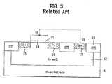
- FIG. 3is a cross sectional view along A-A′ of FIG. 2 .
- an N-well 12is formed in a p-type semiconductor substrate 1 1
- an STI layer 13is formed in a device isolation area of the p-type semiconductor substrate 11 , whereby the semiconductor substrate 11 is divided into an active area and the device isolation area.
- a gate line 14is formed by forming a gate oxide layer 21 on the active area of the semiconductor substrate 11 .
- source and drain 15 and 16are formed at both sides of the gate line 14 in the active area of the semiconductor substrate 11 , wherein the source and drain 15 and 16 are formed in the p-type.
- an ohmic contact layer 17is formed in the active area of the semiconductor substrate 11 , wherein the ohmic contact layer 17 is formed at the predetermined interval from the gate line 14 .
- contacts 18 and 19are respectively formed on the gate line 14 and the ohmic contact layer 17 , wherein the contacts 18 and 19 pass through an insulating interlayer (not shown).
- the contacts 18 and 19are connected with each other by an upper metal layer 20 . That is, the gate line 14 is connected with the N-well 12 through the contact 18 , the metal layer 20 , the contact 19 and the ohmic contact layer 17 .
- the N-well 12becomes a depletion layer.
- the lightis incident on the depletion layer, electron-hole pairs are generated.
- the holesare discharged to the semiconductor substrate 11 , and the electrons are accumulated to the depletion layer.
- the potential of the ohmic contact layer 17is lowered, whereby the potential of the gate line 14 connected with the ohmic contact layer 17 is also lowered. Accordingly, the holes are accumulated to the lower side of the gate line 14 . In proportion to the amount of accumulated holes, more electrons are accumulated to the depletion layer.
- the potential of the ohmic contact layer 17is lowered, and the potential of the gate line 14 is also lowered.
- more holesare accumulated to the lower side of the gate line 14 .
- more electronsare accumulated to the depletion layer.
- the phototransistoris very sensitive to the small amount of light. That is, the phototransistor serves as the photo-sensing means of the great photo-sensitivity.
- the gate line 14is formed at the predetermined interval from the ohmic contact layer 17 . Accordingly, it is necessary to provide the additional area for design of the ohmic contact layer 17 . That is, the entire layout area increases, and the chip size also increases.
- the present inventionis directed to a phototransistor of a CMOS image sensor and a method for fabricating the same that substantially obviates one or more problems due to limitations and disadvantages of the related art.
- An object of the present inventionis to provide a phototransistor of a CMOS image sensor suitable for decreasing the size of layout, and a method for fabricating the phototransistor.
- a phototransistor of a CMOS image sensorincludes a first conductive type semiconductor substrate; an STI layer on the first conductive type semiconductor substrate, to define an active area and a device isolation area in the first conductive type semiconductor substrate; a second conductive type well in the first conductive type semiconductor substrate; a gate line on the first conductive type semiconductor substrate; an ohmic contact layer in the second conductive type well, wherein the ohmic contact layer is overlapped with the gate line in state of interposing the STI layer therebetween; and a contact to connect the gate line with the ohmic contact layer through the STI layer.
- a method for fabricating a phototransistor of a CMOS image sensorincludes the steps of defining an active area and a device isolation area in a first conductive type semiconductor substrate by forming an STI layer in the first conductive type semiconductor substrate; forming a second conductive type well in the first conductive type semiconductor substrate; forming a gate oxide layer on an entire surface of the first conductive type semiconductor substrate; forming a contact hole for exposing the predetermined portion of the second conductive type well below the STI layer by selectively removing the gate oxide layer and the STI layer; forming an ohmic contact layer in the second conductive well below the contact hole; forming a contact by filling the contact hole with a conductive material; and forming a gate line on the first conductive type semiconductor substrate including the contact.
- FIG. 1is a circuit diagram of showing a unit pixel in a 3-T CMOS image sensor according to the related art
- FIG. 2is a layout of a phototransistor according to the related art
- FIG. 3is a cross sectional view along A-A′ of FIG. 2 ;
- FIG. 4is a layout of a phototransistor in a CMOS image sensor according to the present invention.
- FIG. 5is a cross sectional view along B-B′ of FIG. 4 ;
- FIG. 6A to FIG. 6Care cross sectional views of the process for fabricating a phototransistor according to the present invention.
- FIG. 4is a layout of a phototransistor in a CMOS image sensor according to the present invention.
- FIG. 5is a cross sectional view along B-B′ of FIG. 4 .
- an STI layer 32is formed in a device isolation area of a p-type semiconductor substrate 31 .
- the p-type semiconductor substrate 31is divided into an active area and the device isolation area.
- an N-well 33is formed in the semiconductor substrate 31 , wherein the N-well 33 has the predetermined depth.
- a gate oxide layer 34is formed on the predetermined portion of the semiconductor substrate 31 , thereby forming a gate line 38 . Then, source and drain 39 and 40 are formed at both sides of the gate line 38 in the active area of the semiconductor substrate 31 , wherein the source and drain 39 and 40 are doped with p-type.
- an ohmic contact layer 36is formed in the N-well 33 below the STI layer 32 overlapped with the gate line 38 .
- the ohmic contact layer 36is electrically connected with the gate line 38 by a contact 37 through the STI layer 32 .
- the ohmic contact layer 36is partially overlapped with the gate line 38 , whereby it doesn't requires the additional area for design of the ohmic contact layer 36 .
- FIG. 6A to FIG. 6Care cross sectional views of the process for fabricating the phototransistor according to the present invention.
- the STI layer 32is formed in the p-type semiconductor substrate 31 , thereby dividing the semiconductor substrate 31 into the active area and the device isolation area. Then, the N-well 33 having the constant depth is formed in the semiconductor substrate 31 by implantation and diffusion of N-type impurity ions.
- the gate oxide layer 34is formed on the entire surface of the semiconductor substrate 31 including the STI layer 32 . Then, the gate oxide layer 34 and the STI layer 32 are partially removed to expose the N-well 33 below the predetermined portion of the STI layer 32 , thereby forming a contact hole 35 .
- N-type impurity ionsare implanted to the semiconductor substrate 31 in state of using the gate oxide layer 34 as a mask, thereby forming the ohmic contact layer 36 in the N-well 33 below the contact hole 35 .
- a polysilicon layeris coated on the entire surface of the semiconductor substrate 31 including the contact hole 35 , and is then selectively patterned to remain on the predetermined portion including the contact hole 35 , thereby forming the contact 37 inside the contact hole 35 .
- the gate line 38is formed on the gate oxide layer 34 .
- the contact 37 and the gate line 38are formed at the same time. However, it is possible to form the gate line 38 on the predetermined portion including the contact 37 after forming the contact 37 by filling the contact hole 35 with a conductive material.
- p-type impurity ionsare implanted to the active area of the semiconductor substrate 31 in state of using the gate line 38 as a mask, thereby forming the source and drain 39 and 40 . According to the aforementioned process, it is possible to complete the phototransistor of the CMOS image sensor according to the present invention.
- the phototransistor of the CMOS image sensor according to the present inventionhas the following advantages.
- the ohmic contact layeris formed below the gate line. Accordingly, there is no requirement for providing the additional area for design of the ohmic contact layer, so that it is possible to decrease the size of layout.
- the phototransistor of the CMOS image sensor according to the present inventiondoesn't requires a metal line for connecting the ohmic contact layer with the gate line, thereby obtaining the simplified fabrication process.
Landscapes
- Solid State Image Pick-Up Elements (AREA)
Abstract
Description
- This application claims the benefit of Korean Application No. P2004-52006 filed on Jul. 5, 2004, which is hereby incorporated by reference as if fully set forth herein.
- 1. Field of the Invention
- The present invention relates to a CMOS image sensor, and more particularly, to a phototransistor of a CMOS image sensor suitable for decreasing the size of layout, and a method for fabricating the phototransistor.
- 2. Discussion of the Related Art
- Generally, an image sensor is a semiconductor device for converting an optical image into an electric signal. The image sensor can be broadly categorized into a charge coupled device (CCD) and a complementary metal oxide semiconductor (CMOS) image sensor.
- In case of the CCD, respective metal-oxide-silicon MOS capacitors are positioned adjacently, wherein electric charge carriers are stored in and transferred to the capacitors. Meanwhile, the CMOS image sensor adopts the CMOS technology of using a control circuit and a signal processing circuit as the circumferential circuit. The CMOS image sensor uses the switching method of sequentially detecting output signals by forming the predetermined number of MOS transistors in correspondence with the number of pixels.
- The CCD has the high power consumption and the complicated mask process. Also, it is impossible to provide the signal processing circuit inside the CCD chip, whereby it cannot be formed in one chip. In order to overcome these problems, the sub-micron CMOS fabrication technology has been researched and developed.
- In the CMOS image sensor, the photo-sensing means is generally formed of a photodiode. Recently, instead of the photodiode, a phototransistor is used for the photo-sensing means, to improve the photo-sensing degree.
FIG. 1 is a circuit diagram of showing a unit pixel in a 3-T CMOS image sensor according to the related art.- As shown in
FIG. 1 , a unit pixel of a 3-T CMOS image sensor according to the related art is comprised of a phototransistor PT, and three NMOS transistors Rx, Dx and Sx. - The phototransistor PT is formed as a PMOS transistor structure in which a gate is connected with a semiconductor substrate. Accordingly, when the light is incident on the phototransistor PT, electrons are accumulated on the semiconductor substrate, whereby a gate potential is lowered. Due to the lowered gate potential, holes are accumulated to the lower side of gate. In proportion to the amount of accumulated holes, more electrons are accumulated to the semiconductor substrate. Thus, the gate potential becomes lower. As a result, the phototransistor PT functions as the photo-sensing means having the great photo-photosensitivity according to the repetitive mechanism. That is, the phototransistor PT is very sensitive to the small amount of light.
- Among the three NMOS transistors, the reset transistor Rx discharges the electrons stored in a floating sensing node FSN to detect the signal. The drive transistor Dx changes an output voltage of a unit pixel by changing a current of a source follower according to the change on the potential of the floating sensing node FSN. The select transistor Sx is provided for switching and addressing.
- In addition, a DC gate is a load transistor, which has a gate having a constant voltage applied thereto. That is, since the constant voltage is applied to the gate of the transistor, a constant current flows through the DC gate. Also, ‘VDD’ is a drive power voltage, ‘GND’ is a ground voltage, and ‘Signal Out’ is an output voltage of a unit pixel.
- Hereinafter, a phototransistor of a CMOS image sensor according to the related art will be described with reference to the accompanying drawings.
FIG. 2 is a layout of a phototransistor according to the related art.FIG. 3 is a cross sectional view along A-A′ ofFIG. 2 .- As shown in
FIG. 2 andFIG. 3 , an N-well 12 is formed in a p-type semiconductor substrate11, and anSTI layer 13 is formed in a device isolation area of the p-type semiconductor substrate 11, whereby thesemiconductor substrate 11 is divided into an active area and the device isolation area. - After that, a
gate line 14 is formed by forming agate oxide layer 21 on the active area of thesemiconductor substrate 11. Then, source anddrain gate line 14 in the active area of thesemiconductor substrate 11, wherein the source anddrain ohmic contact layer 17 is formed in the active area of thesemiconductor substrate 11, wherein theohmic contact layer 17 is formed at the predetermined interval from thegate line 14. - Then,
contacts gate line 14 and theohmic contact layer 17, wherein thecontacts contacts upper metal layer 20. That is, thegate line 14 is connected with the N-well 12 through thecontact 18, themetal layer 20, thecontact 19 and theohmic contact layer 17. - If applying a reverse bias to the N-
well 12, the N-well 12 becomes a depletion layer. When the light is incident on the depletion layer, electron-hole pairs are generated. In this state, the holes are discharged to thesemiconductor substrate 11, and the electrons are accumulated to the depletion layer. - As the electrons are accumulated to the depletion layer, the potential of the
ohmic contact layer 17 is lowered, whereby the potential of thegate line 14 connected with theohmic contact layer 17 is also lowered. Accordingly, the holes are accumulated to the lower side of thegate line 14. In proportion to the amount of accumulated holes, more electrons are accumulated to the depletion layer. - Accordingly, the potential of the
ohmic contact layer 17 is lowered, and the potential of thegate line 14 is also lowered. Thus, more holes are accumulated to the lower side of thegate line 14. In proportion to the amount of accumulated holes, more electrons are accumulated to the depletion layer. - According to the repetitive mechanism, the phototransistor is very sensitive to the small amount of light. That is, the phototransistor serves as the photo-sensing means of the great photo-sensitivity.
- However, the related art phototransistor has the following disadvantages.
- In the related art phototransistor, the
gate line 14 is formed at the predetermined interval from theohmic contact layer 17. Accordingly, it is necessary to provide the additional area for design of theohmic contact layer 17. That is, the entire layout area increases, and the chip size also increases. - Accordingly, the present invention is directed to a phototransistor of a CMOS image sensor and a method for fabricating the same that substantially obviates one or more problems due to limitations and disadvantages of the related art.
- An object of the present invention is to provide a phototransistor of a CMOS image sensor suitable for decreasing the size of layout, and a method for fabricating the phototransistor.
- Additional advantages, objects, and features of the invention will be set forth in part in the description which follows and in part will become apparent to those having ordinary skill in the art upon examination of the following or may be learned from practice of the invention. The objectives and other advantages of the invention may be realized and attained by the structure particularly pointed out in the written description and claims hereof as well as the appended drawings.
- To achieve these objects and other advantages and in accordance with the purpose of the invention, as embodied and broadly described herein, a phototransistor of a CMOS image sensor includes a first conductive type semiconductor substrate; an STI layer on the first conductive type semiconductor substrate, to define an active area and a device isolation area in the first conductive type semiconductor substrate; a second conductive type well in the first conductive type semiconductor substrate; a gate line on the first conductive type semiconductor substrate; an ohmic contact layer in the second conductive type well, wherein the ohmic contact layer is overlapped with the gate line in state of interposing the STI layer therebetween; and a contact to connect the gate line with the ohmic contact layer through the STI layer.
- In another aspect, a method for fabricating a phototransistor of a CMOS image sensor includes the steps of defining an active area and a device isolation area in a first conductive type semiconductor substrate by forming an STI layer in the first conductive type semiconductor substrate; forming a second conductive type well in the first conductive type semiconductor substrate; forming a gate oxide layer on an entire surface of the first conductive type semiconductor substrate; forming a contact hole for exposing the predetermined portion of the second conductive type well below the STI layer by selectively removing the gate oxide layer and the STI layer; forming an ohmic contact layer in the second conductive well below the contact hole; forming a contact by filling the contact hole with a conductive material; and forming a gate line on the first conductive type semiconductor substrate including the contact.
- It is to be understood that both the foregoing general description and the following detailed description of the present invention are exemplary and explanatory and are intended to provide further explanation of the invention as claimed.
- The accompanying drawings, which are included to provide a further understanding of the invention and are incorporated in and constitute a part of this application, illustrate embodiments of the invention and together with the description serve to explain the principle of the invention. In the drawings:
FIG. 1 is a circuit diagram of showing a unit pixel in a 3-T CMOS image sensor according to the related art;FIG. 2 is a layout of a phototransistor according to the related art;FIG. 3 is a cross sectional view along A-A′ ofFIG. 2 ;FIG. 4 is a layout of a phototransistor in a CMOS image sensor according to the present invention;FIG. 5 is a cross sectional view along B-B′ ofFIG. 4 ; andFIG. 6A toFIG. 6C are cross sectional views of the process for fabricating a phototransistor according to the present invention.- Reference will now be made in detail to the preferred embodiments of the present invention, examples of which are illustrated in the accompanying drawings. Wherever possible, the same reference numbers will be used throughout the drawings to refer to the same or like parts.
- Hereinafter, a phototransistor of a CMOS image sensor according to the present invention will be described with reference to the accompanying drawings.
FIG. 4 is a layout of a phototransistor in a CMOS image sensor according to the present invention.FIG. 5 is a cross sectional view along B-B′ ofFIG. 4 .- In a phototransistor of a CMOS image sensor according to the present invention, as shown in
FIG. 4 andFIG. 5 , anSTI layer 32 is formed in a device isolation area of a p-type semiconductor substrate 31. As a result, the p-type semiconductor substrate 31 is divided into an active area and the device isolation area. Also, an N-well 33 is formed in thesemiconductor substrate 31, wherein the N-well 33 has the predetermined depth. - Also, a
gate oxide layer 34 is formed on the predetermined portion of thesemiconductor substrate 31, thereby forming agate line 38. Then, source and drain39 and40 are formed at both sides of thegate line 38 in the active area of thesemiconductor substrate 31, wherein the source and drain39 and40 are doped with p-type. - In addition, an
ohmic contact layer 36 is formed in the N-well33 below theSTI layer 32 overlapped with thegate line 38. Theohmic contact layer 36 is electrically connected with thegate line 38 by acontact 37 through theSTI layer 32. - In the phototransistor of the CMOS image sensor according to the present invention, the
ohmic contact layer 36 is partially overlapped with thegate line 38, whereby it doesn't requires the additional area for design of theohmic contact layer 36. - A method for fabricating the phototransistor according to the present invention will be described with reference to the accompanying drawings.
FIG. 6A toFIG. 6C are cross sectional views of the process for fabricating the phototransistor according to the present invention.- First, as shown in
FIG. 6A , theSTI layer 32 is formed in the p-type semiconductor substrate 31, thereby dividing thesemiconductor substrate 31 into the active area and the device isolation area. Then, the N-well33 having the constant depth is formed in thesemiconductor substrate 31 by implantation and diffusion of N-type impurity ions. - Referring to
FIG. 6B , thegate oxide layer 34 is formed on the entire surface of thesemiconductor substrate 31 including theSTI layer 32. Then, thegate oxide layer 34 and theSTI layer 32 are partially removed to expose the N-well33 below the predetermined portion of theSTI layer 32, thereby forming acontact hole 35. - Subsequently, N-type impurity ions are implanted to the
semiconductor substrate 31 in state of using thegate oxide layer 34 as a mask, thereby forming theohmic contact layer 36 in the N-well33 below thecontact hole 35. - Then, a polysilicon layer is coated on the entire surface of the
semiconductor substrate 31 including thecontact hole 35, and is then selectively patterned to remain on the predetermined portion including thecontact hole 35, thereby forming thecontact 37 inside thecontact hole 35. Then, thegate line 38 is formed on thegate oxide layer 34. - Herein, the
contact 37 and thegate line 38 are formed at the same time. However, it is possible to form thegate line 38 on the predetermined portion including thecontact 37 after forming thecontact 37 by filling thecontact hole 35 with a conductive material. - Although not shown, p-type impurity ions are implanted to the active area of the
semiconductor substrate 31 in state of using thegate line 38 as a mask, thereby forming the source and drain39 and40. According to the aforementioned process, it is possible to complete the phototransistor of the CMOS image sensor according to the present invention. - As mentioned above, the phototransistor of the CMOS image sensor according to the present invention has the following advantages.
- In the phototransistor of the CMOS image sensor according to the present invention, the ohmic contact layer is formed below the gate line. Accordingly, there is no requirement for providing the additional area for design of the ohmic contact layer, so that it is possible to decrease the size of layout.
- Also, the phototransistor of the CMOS image sensor according to the present invention doesn't requires a metal line for connecting the ohmic contact layer with the gate line, thereby obtaining the simplified fabrication process.
- It will be apparent to those skilled in the art that various modifications and variations can be made in the present invention without departing from the spirit or scope of the inventions. Thus, it is intended that the present invention covers the modifications and variations of this invention provided they come within the scope of the appended claims and their equivalents.
Claims (7)
Applications Claiming Priority (2)
| Application Number | Priority Date | Filing Date | Title |
|---|---|---|---|
| KRP2004-52006 | 2004-07-05 | ||
| KR1020040052006AKR100577312B1 (en) | 2004-07-05 | 2004-07-05 | Phototransistor of CMOS image sensor and its manufacturing method |
Publications (2)
| Publication Number | Publication Date |
|---|---|
| US20060001121A1true US20060001121A1 (en) | 2006-01-05 |
| US7229878B2 US7229878B2 (en) | 2007-06-12 |
Family
ID=35513017
Family Applications (1)
| Application Number | Title | Priority Date | Filing Date |
|---|---|---|---|
| US11/175,524Expired - Fee RelatedUS7229878B2 (en) | 2004-07-05 | 2005-07-05 | Phototransistor of CMOS image sensor and method for fabricating the same |
Country Status (2)
| Country | Link |
|---|---|
| US (1) | US7229878B2 (en) |
| KR (1) | KR100577312B1 (en) |
Cited By (3)
| Publication number | Priority date | Publication date | Assignee | Title |
|---|---|---|---|---|
| US20060138549A1 (en)* | 2004-12-29 | 2006-06-29 | Ko Kwang Y | High-voltage transistor and fabricating method thereof |
| US20090065824A1 (en)* | 2007-09-07 | 2009-03-12 | Joon Hwang | Image Sensor and Manufacturing Method Thereof |
| US20130113047A1 (en)* | 2011-11-03 | 2013-05-09 | Taiwan Semiconductor Manufacturing Co., Ltd. | Mosfet structure with t-shaped epitaxial silicon channel |
Families Citing this family (11)
| Publication number | Priority date | Publication date | Assignee | Title |
|---|---|---|---|---|
| KR100640964B1 (en)* | 2004-12-30 | 2006-11-02 | 동부일렉트로닉스 주식회사 | Unit pixel circuit of CMOS image sensor |
| KR100884903B1 (en)* | 2007-09-06 | 2009-02-19 | 주식회사 동부하이텍 | Image sensor and its manufacturing method |
| JP2009065160A (en) | 2007-09-06 | 2009-03-26 | Dongbu Hitek Co Ltd | Image sensor and manufacturing method thereof |
| KR100882979B1 (en)* | 2007-09-07 | 2009-02-12 | 주식회사 동부하이텍 | Image sensor and manufacturing method |
| KR100882987B1 (en)* | 2008-06-13 | 2009-02-12 | 주식회사 동부하이텍 | Image sensor and manufacturing method |
| JP5451098B2 (en)* | 2009-02-06 | 2014-03-26 | キヤノン株式会社 | Manufacturing method of semiconductor device |
| JP2010206173A (en) | 2009-02-06 | 2010-09-16 | Canon Inc | Photoelectric conversion device and camera |
| JP2010206172A (en) | 2009-02-06 | 2010-09-16 | Canon Inc | Image sensing device, and camera |
| JP2010206174A (en) | 2009-02-06 | 2010-09-16 | Canon Inc | Photoelectric converter, method of manufacturing the same, and camera |
| US20120280109A1 (en)* | 2011-05-05 | 2012-11-08 | Omnivision Technologies, Inc. | Method, apparatus and system to provide conductivity for a substrate of an image sensing pixel |
| CN103646955A (en)* | 2013-12-18 | 2014-03-19 | 北京思比科微电子技术股份有限公司 | Charge residue reducing backside imaging sensor structure and manufacturing method thereof |
Citations (19)
| Publication number | Priority date | Publication date | Assignee | Title |
|---|---|---|---|---|
| US5841126A (en)* | 1994-01-28 | 1998-11-24 | California Institute Of Technology | CMOS active pixel sensor type imaging system on a chip |
| US5886659A (en)* | 1996-08-21 | 1999-03-23 | California Institute Of Technology | On-focal-plane analog-to-digital conversion for current-mode imaging devices |
| US5990506A (en)* | 1996-03-20 | 1999-11-23 | California Institute Of Technology | Active pixel sensors with substantially planarized color filtering elements |
| US6005619A (en)* | 1997-10-06 | 1999-12-21 | Photobit Corporation | Quantum efficiency improvements in active pixel sensors |
| US6021172A (en)* | 1994-01-28 | 2000-02-01 | California Institute Of Technology | Active pixel sensor having intra-pixel charge transfer with analog-to-digital converter |
| US6261908B1 (en)* | 1998-07-27 | 2001-07-17 | Advanced Micro Devices, Inc. | Buried local interconnect |
| US6261920B1 (en)* | 1998-09-04 | 2001-07-17 | Kabushiki Kaisha Toshiba | N-channel MOSFET having STI structure and method for manufacturing the same |
| US20010010938A1 (en)* | 1998-08-31 | 2001-08-02 | Bronner Gary Bela | Diode connected to a magnetic tunnel junction and self aligned with a metallic conductor and method of forming the same |
| US20020024092A1 (en)* | 2000-08-11 | 2002-02-28 | Herbert Palm | Memory cell, memory cell arrangement and fabrication method |
| US6462365B1 (en)* | 2001-11-06 | 2002-10-08 | Omnivision Technologies, Inc. | Active pixel having reduced dark current in a CMOS image sensor |
| US20030020119A1 (en)* | 2001-07-25 | 2003-01-30 | Kabushiki Kaisha Toshiba | Semiconductor device and method of fabricating the same |
| US6613690B1 (en)* | 2002-07-17 | 2003-09-02 | Taiwan Semiconductor Manufacturing Company | Approach for forming a buried stack capacitor structure featuring reduced polysilicon stringers |
| US6849886B1 (en)* | 2003-09-22 | 2005-02-01 | Dongbu Electronics Co., Ltd. | CMOS image sensor and method for manufacturing the same |
| US20050064620A1 (en)* | 2003-09-22 | 2005-03-24 | Han Chang Hun | CMOS image sensor and method for manufacturing the same |
| US20050064665A1 (en)* | 2003-09-23 | 2005-03-24 | Han Chang Hun | Method for manufacturing a CMOS image sensor |
| US20050088556A1 (en)* | 2003-10-28 | 2005-04-28 | Han Chang H. | CMOS image sensor and method for fabricating the same |
| US20050093036A1 (en)* | 2003-11-04 | 2005-05-05 | Dongbu Electronics Co., Ltd. | CMOS image sensor and method for fabricating the same |
| US20050179093A1 (en)* | 2004-02-17 | 2005-08-18 | Silicon Space Technology Corporation | Buried guard ring and radiation hardened isolation structures and fabrication methods |
| US20060124982A1 (en)* | 2004-12-15 | 2006-06-15 | International Business Machines Corporation | Low-Cost Deep Trench Decoupling Capacitor Device and Process of Manufacture |
- 2004
- 2004-07-05KRKR1020040052006Apatent/KR100577312B1/ennot_activeExpired - Fee Related
- 2005
- 2005-07-05USUS11/175,524patent/US7229878B2/ennot_activeExpired - Fee Related
Patent Citations (19)
| Publication number | Priority date | Publication date | Assignee | Title |
|---|---|---|---|---|
| US5841126A (en)* | 1994-01-28 | 1998-11-24 | California Institute Of Technology | CMOS active pixel sensor type imaging system on a chip |
| US6021172A (en)* | 1994-01-28 | 2000-02-01 | California Institute Of Technology | Active pixel sensor having intra-pixel charge transfer with analog-to-digital converter |
| US5990506A (en)* | 1996-03-20 | 1999-11-23 | California Institute Of Technology | Active pixel sensors with substantially planarized color filtering elements |
| US5886659A (en)* | 1996-08-21 | 1999-03-23 | California Institute Of Technology | On-focal-plane analog-to-digital conversion for current-mode imaging devices |
| US6005619A (en)* | 1997-10-06 | 1999-12-21 | Photobit Corporation | Quantum efficiency improvements in active pixel sensors |
| US6261908B1 (en)* | 1998-07-27 | 2001-07-17 | Advanced Micro Devices, Inc. | Buried local interconnect |
| US20010010938A1 (en)* | 1998-08-31 | 2001-08-02 | Bronner Gary Bela | Diode connected to a magnetic tunnel junction and self aligned with a metallic conductor and method of forming the same |
| US6261920B1 (en)* | 1998-09-04 | 2001-07-17 | Kabushiki Kaisha Toshiba | N-channel MOSFET having STI structure and method for manufacturing the same |
| US20020024092A1 (en)* | 2000-08-11 | 2002-02-28 | Herbert Palm | Memory cell, memory cell arrangement and fabrication method |
| US20030020119A1 (en)* | 2001-07-25 | 2003-01-30 | Kabushiki Kaisha Toshiba | Semiconductor device and method of fabricating the same |
| US6462365B1 (en)* | 2001-11-06 | 2002-10-08 | Omnivision Technologies, Inc. | Active pixel having reduced dark current in a CMOS image sensor |
| US6613690B1 (en)* | 2002-07-17 | 2003-09-02 | Taiwan Semiconductor Manufacturing Company | Approach for forming a buried stack capacitor structure featuring reduced polysilicon stringers |
| US6849886B1 (en)* | 2003-09-22 | 2005-02-01 | Dongbu Electronics Co., Ltd. | CMOS image sensor and method for manufacturing the same |
| US20050064620A1 (en)* | 2003-09-22 | 2005-03-24 | Han Chang Hun | CMOS image sensor and method for manufacturing the same |
| US20050064665A1 (en)* | 2003-09-23 | 2005-03-24 | Han Chang Hun | Method for manufacturing a CMOS image sensor |
| US20050088556A1 (en)* | 2003-10-28 | 2005-04-28 | Han Chang H. | CMOS image sensor and method for fabricating the same |
| US20050093036A1 (en)* | 2003-11-04 | 2005-05-05 | Dongbu Electronics Co., Ltd. | CMOS image sensor and method for fabricating the same |
| US20050179093A1 (en)* | 2004-02-17 | 2005-08-18 | Silicon Space Technology Corporation | Buried guard ring and radiation hardened isolation structures and fabrication methods |
| US20060124982A1 (en)* | 2004-12-15 | 2006-06-15 | International Business Machines Corporation | Low-Cost Deep Trench Decoupling Capacitor Device and Process of Manufacture |
Cited By (6)
| Publication number | Priority date | Publication date | Assignee | Title |
|---|---|---|---|---|
| US20060138549A1 (en)* | 2004-12-29 | 2006-06-29 | Ko Kwang Y | High-voltage transistor and fabricating method thereof |
| US20090065824A1 (en)* | 2007-09-07 | 2009-03-12 | Joon Hwang | Image Sensor and Manufacturing Method Thereof |
| US7999292B2 (en) | 2007-09-07 | 2011-08-16 | Dongbu Hitek Co., Ltd. | Image sensor and manufacturing method thereof |
| US20130113047A1 (en)* | 2011-11-03 | 2013-05-09 | Taiwan Semiconductor Manufacturing Co., Ltd. | Mosfet structure with t-shaped epitaxial silicon channel |
| US9000526B2 (en)* | 2011-11-03 | 2015-04-07 | Taiwan Semiconductor Manufacturing Co., Ltd. | MOSFET structure with T-shaped epitaxial silicon channel |
| US9653545B2 (en) | 2011-11-03 | 2017-05-16 | Taiwan Semiconductor Manufacturing Co., Ltd. | MOSFET structure with T-shaped epitaxial silicon channel |
Also Published As
| Publication number | Publication date |
|---|---|
| KR20060003201A (en) | 2006-01-10 |
| KR100577312B1 (en) | 2006-05-10 |
| US7229878B2 (en) | 2007-06-12 |
Similar Documents
| Publication | Publication Date | Title |
|---|---|---|
| US7884401B2 (en) | CMOS image sensor and manufacturing method thereof | |
| JP5426114B2 (en) | Semiconductor device and manufacturing method thereof | |
| US7772624B2 (en) | Image sensors and methods of fabricating same | |
| US6734471B2 (en) | Image sensor having photo diode and method for manufacturing the same | |
| US7459335B2 (en) | Solid-state imaging apparatus and method for producing the same | |
| JP2002280538A (en) | CMOS image sensor capable of complete pixel reset without kTC noise | |
| US7229878B2 (en) | Phototransistor of CMOS image sensor and method for fabricating the same | |
| US7678643B2 (en) | Method for manufacturing a CMOS image sensor | |
| US7611918B2 (en) | CMOS image sensor and method for fabricating the same | |
| US7670864B2 (en) | CMOS image sensor and fabricating method thereof | |
| KR100760913B1 (en) | CMOS image sensor and its manufacturing method | |
| US20050139878A1 (en) | CMOS image sensor and method for fabricating the same | |
| US7354841B2 (en) | Method for fabricating photodiode of CMOS image sensor | |
| US20070246757A1 (en) | CMOS image sensor and method for fabricating the same | |
| US20060001062A1 (en) | Method for fabricating CMOS image sensor | |
| US20080042170A1 (en) | Image Sensor and Method for Manufacturing the Same | |
| US7413944B2 (en) | CMOS image sensor and method of manufacturing the same | |
| US20070145423A1 (en) | CMOS Image Sensor and Manufacturing Method Thereof | |
| JP2007150361A (en) | Method for manufacturing solid-state imaging device | |
| KR100321768B1 (en) | method for fabricating Unit pixel with negative substrate voltage in CMOS image sensor | |
| KR100672715B1 (en) | CMOS image sensor and method for fabricating the same | |
| KR100321769B1 (en) | Unit pixel with negative substrate voltage in CMOS image sensor | |
| KR20020058458A (en) | Image sensor capable of increasing effective area of photodiode and method for fabricating the same | |
| KR20060127498A (en) | Manufacturing Method of CMOS Image Sensor for Reducing Dark Current | |
| KR20030001128A (en) | Image sensor and fabricating method of the same |
Legal Events
| Date | Code | Title | Description |
|---|---|---|---|
| AS | Assignment | Owner name:DONGBUANAM SEMICONDUCTOR INC., KOREA, REPUBLIC OF Free format text:ASSIGNMENT OF ASSIGNORS INTEREST;ASSIGNOR:JEON, IN GYUN;REEL/FRAME:016766/0643 Effective date:20050704 | |
| AS | Assignment | Owner name:DONGBU ELECTRONICS CO., LTD.,KOREA, REPUBLIC OF Free format text:CHANGE OF NAME;ASSIGNOR:DONGANAM SEMICONDUCTOR INC.;REEL/FRAME:017654/0078 Effective date:20060328 Owner name:DONGBU ELECTRONICS CO., LTD., KOREA, REPUBLIC OF Free format text:CHANGE OF NAME;ASSIGNOR:DONGANAM SEMICONDUCTOR INC.;REEL/FRAME:017654/0078 Effective date:20060328 | |
| AS | Assignment | Owner name:DONGBU ELECTRONICS CO., LTD., KOREA, REPUBLIC OF Free format text:CORRECTIVE ASSIGNMENT TO CORRECT THE ASSIGNOR PREVIOUSLY RECORDED ON REEL 017654 FRAME 0078;ASSIGNOR:DONGBUANAM SEMICONDUCTOR INC.;REEL/FRAME:017829/0911 Effective date:20060328 Owner name:DONGBU ELECTRONICS CO., LTD.,KOREA, REPUBLIC OF Free format text:CORRECTIVE ASSIGNMENT TO CORRECT THE ASSIGNOR PREVIOUSLY RECORDED ON REEL 017654 FRAME 0078. ASSIGNOR(S) HEREBY CONFIRMS THE ASSIGNOR SHOULD BE "DONGBUANAM SEMICONDUCTOR INC.";ASSIGNOR:DONGBUANAM SEMICONDUCTOR INC.;REEL/FRAME:017829/0911 Effective date:20060328 Owner name:DONGBU ELECTRONICS CO., LTD., KOREA, REPUBLIC OF Free format text:CORRECTIVE ASSIGNMENT TO CORRECT THE ASSIGNOR PREVIOUSLY RECORDED ON REEL 017654 FRAME 0078. ASSIGNOR(S) HEREBY CONFIRMS THE ASSIGNOR SHOULD BE "DONGBUANAM SEMICONDUCTOR INC.";ASSIGNOR:DONGBUANAM SEMICONDUCTOR INC.;REEL/FRAME:017829/0911 Effective date:20060328 | |
| FEPP | Fee payment procedure | Free format text:PAYOR NUMBER ASSIGNED (ORIGINAL EVENT CODE: ASPN); ENTITY STATUS OF PATENT OWNER: LARGE ENTITY | |
| FEPP | Fee payment procedure | Free format text:PAYER NUMBER DE-ASSIGNED (ORIGINAL EVENT CODE: RMPN); ENTITY STATUS OF PATENT OWNER: LARGE ENTITY Free format text:PAYOR NUMBER ASSIGNED (ORIGINAL EVENT CODE: ASPN); ENTITY STATUS OF PATENT OWNER: LARGE ENTITY | |
| FPAY | Fee payment | Year of fee payment:4 | |
| REMI | Maintenance fee reminder mailed | ||
| LAPS | Lapse for failure to pay maintenance fees | ||
| STCH | Information on status: patent discontinuation | Free format text:PATENT EXPIRED DUE TO NONPAYMENT OF MAINTENANCE FEES UNDER 37 CFR 1.362 | |
| FP | Lapsed due to failure to pay maintenance fee | Effective date:20150612 |