US20050287728A1 - Method for forming a bottom gate thin film transistor using a blend solution to form a semiconducting layer and an insulating layer - Google Patents
Method for forming a bottom gate thin film transistor using a blend solution to form a semiconducting layer and an insulating layerDownload PDFInfo
- Publication number
- US20050287728A1 US20050287728A1US10/876,229US87622904AUS2005287728A1US 20050287728 A1US20050287728 A1US 20050287728A1US 87622904 AUS87622904 AUS 87622904AUS 2005287728 A1US2005287728 A1US 2005287728A1
- Authority
- US
- United States
- Prior art keywords
- polymer
- blend solution
- substrate
- insulator
- thin film
- Prior art date
- Legal status (The legal status is an assumption and is not a legal conclusion. Google has not performed a legal analysis and makes no representation as to the accuracy of the status listed.)
- Granted
Links
- 238000000034methodMethods0.000titleclaimsabstractdescription49
- 239000000203mixtureSubstances0.000titleclaimsdescription29
- OFIYHXOOOISSDN-UHFFFAOYSA-NtellanylidenegalliumChemical compound[Te]=[Ga]OFIYHXOOOISSDN-UHFFFAOYSA-N0.000titleclaimsdescription7
- 229920000642polymerPolymers0.000claimsabstractdescription127
- 239000002904solventSubstances0.000claimsabstractdescription45
- 239000000758substrateSubstances0.000claimsabstractdescription42
- 239000004065semiconductorSubstances0.000claimsabstractdescription21
- 239000000463materialSubstances0.000claimsabstractdescription20
- 239000012212insulatorSubstances0.000claimsdescription36
- 229920002959polymer blendPolymers0.000claimsdescription29
- 239000004020conductorSubstances0.000claimsdescription28
- 238000000151depositionMethods0.000claimsdescription21
- 239000010409thin filmSubstances0.000claimsdescription14
- 230000008021depositionEffects0.000claimsdescription12
- 239000011810insulating materialSubstances0.000claimsdescription11
- 239000002243precursorSubstances0.000claimsdescription11
- 229920003229poly(methyl methacrylate)Polymers0.000claimsdescription7
- 239000004926polymethyl methacrylateSubstances0.000claimsdescription7
- 238000004519manufacturing processMethods0.000claimsdescription6
- DZUNDTRLGXGTGU-UHFFFAOYSA-N2-(3-dodecylthiophen-2-yl)-5-[5-(3-dodecylthiophen-2-yl)thiophen-2-yl]thiopheneChemical compoundC1=CSC(C=2SC(=CC=2)C=2SC(=CC=2)C2=C(C=CS2)CCCCCCCCCCCC)=C1CCCCCCCCCCCCDZUNDTRLGXGTGU-UHFFFAOYSA-N0.000claimsdescription3
- 238000007639printingMethods0.000claimsdescription3
- 229920000123polythiophenePolymers0.000claimsdescription2
- 238000001704evaporationMethods0.000abstractdescription2
- 230000008020evaporationEffects0.000abstractdescription2
- 239000010410layerSubstances0.000description40
- -1poly(3-n-hexylthiophene)Polymers0.000description9
- 230000015572biosynthetic processEffects0.000description7
- 238000005538encapsulationMethods0.000description7
- 239000000178monomerSubstances0.000description7
- UMIVXZPTRXBADB-UHFFFAOYSA-NbenzocyclobuteneChemical compoundC1=CC=C2CCC2=C1UMIVXZPTRXBADB-UHFFFAOYSA-N0.000description6
- 239000010408filmSubstances0.000description6
- 239000007788liquidSubstances0.000description6
- 230000008569processEffects0.000description6
- 238000000935solvent evaporationMethods0.000description6
- 230000007613environmental effectEffects0.000description5
- 229920006254polymer filmPolymers0.000description5
- HEDRZPFGACZZDS-UHFFFAOYSA-NChloroformChemical compoundClC(Cl)ClHEDRZPFGACZZDS-UHFFFAOYSA-N0.000description4
- 238000009835boilingMethods0.000description4
- 238000004581coalescenceMethods0.000description4
- 230000037230mobilityEffects0.000description4
- 238000000926separation methodMethods0.000description4
- 238000004528spin coatingMethods0.000description4
- OCJBOOLMMGQPQU-UHFFFAOYSA-N1,4-dichlorobenzeneChemical compoundClC1=CC=C(Cl)C=C1OCJBOOLMMGQPQU-UHFFFAOYSA-N0.000description3
- 239000004642PolyimideSubstances0.000description3
- 238000000137annealingMethods0.000description3
- 230000015556catabolic processEffects0.000description3
- 238000006731degradation reactionMethods0.000description3
- 229940117389dichlorobenzeneDrugs0.000description3
- 230000003993interactionEffects0.000description3
- 239000003960organic solventSubstances0.000description3
- 238000005191phase separationMethods0.000description3
- 229920001721polyimidePolymers0.000description3
- 230000009466transformationEffects0.000description3
- CTQNGGLPUBDAKN-UHFFFAOYSA-NO-XyleneChemical compoundCC1=CC=CC=C1CCTQNGGLPUBDAKN-UHFFFAOYSA-N0.000description2
- 229920001609Poly(3,4-ethylenedioxythiophene)Polymers0.000description2
- GTDPSWPPOUPBNX-UHFFFAOYSA-Nac1mqpvaChemical compoundCC12C(=O)OC(=O)C1(C)C1(C)C2(C)C(=O)OC1=OGTDPSWPPOUPBNX-UHFFFAOYSA-N0.000description2
- 238000005266castingMethods0.000description2
- 150000001875compoundsChemical class0.000description2
- 239000002322conducting polymerSubstances0.000description2
- 229920001940conductive polymerPolymers0.000description2
- 150000004985diaminesChemical class0.000description2
- 238000009792diffusion processMethods0.000description2
- 230000007246mechanismEffects0.000description2
- AUHZEENZYGFFBQ-UHFFFAOYSA-NmesityleneSubstancesCC1=CC(C)=CC(C)=C1AUHZEENZYGFFBQ-UHFFFAOYSA-N0.000description2
- 125000001827mesitylenyl groupChemical group[H]C1=C(C(*)=C(C([H])=C1C([H])([H])[H])C([H])([H])[H])C([H])([H])[H]0.000description2
- 229910052751metalInorganic materials0.000description2
- 239000002184metalSubstances0.000description2
- 238000012986modificationMethods0.000description2
- 230000004048modificationEffects0.000description2
- 239000012071phaseSubstances0.000description2
- 229920000767polyanilinePolymers0.000description2
- 150000003573thiolsChemical class0.000description2
- 238000009736wettingMethods0.000description2
- 239000008096xyleneSubstances0.000description2
- OKTJSMMVPCPJKN-UHFFFAOYSA-NCarbonChemical compound[C]OKTJSMMVPCPJKN-UHFFFAOYSA-N0.000description1
- RYGMFSIKBFXOCR-UHFFFAOYSA-NCopperChemical compound[Cu]RYGMFSIKBFXOCR-UHFFFAOYSA-N0.000description1
- 239000005456alcohol based solventSubstances0.000description1
- HSFWRNGVRCDJHI-UHFFFAOYSA-Nalpha-acetyleneNatural productsC#CHSFWRNGVRCDJHI-UHFFFAOYSA-N0.000description1
- 229910052782aluminiumInorganic materials0.000description1
- XAGFODPZIPBFFR-UHFFFAOYSA-NaluminiumChemical compound[Al]XAGFODPZIPBFFR-UHFFFAOYSA-N0.000description1
- QVGXLLKOCUKJST-UHFFFAOYSA-Natomic oxygenChemical compound[O]QVGXLLKOCUKJST-UHFFFAOYSA-N0.000description1
- 230000004888barrier functionEffects0.000description1
- 239000002041carbon nanotubeSubstances0.000description1
- 229910021393carbon nanotubeInorganic materials0.000description1
- 238000001246colloidal dispersionMethods0.000description1
- 239000000470constituentSubstances0.000description1
- 229910052802copperInorganic materials0.000description1
- 239000010949copperSubstances0.000description1
- 230000008878couplingEffects0.000description1
- 238000010168coupling processMethods0.000description1
- 238000005859coupling reactionMethods0.000description1
- 230000001066destructive effectEffects0.000description1
- 238000003618dip coatingMethods0.000description1
- 125000002534ethynyl groupChemical group[H]C#C*0.000description1
- 230000005669field effectEffects0.000description1
- 229910052737goldInorganic materials0.000description1
- 238000010438heat treatmentMethods0.000description1
- 239000011261inert gasSubstances0.000description1
- 238000007641inkjet printingMethods0.000description1
- 230000002452interceptive effectEffects0.000description1
- 238000001540jet depositionMethods0.000description1
- 239000007791liquid phaseSubstances0.000description1
- 230000007774longtermEffects0.000description1
- 238000004020luminiscence typeMethods0.000description1
- 238000005297material degradation processMethods0.000description1
- 239000002082metal nanoparticleSubstances0.000description1
- 229910052760oxygenInorganic materials0.000description1
- 239000001301oxygenSubstances0.000description1
- 238000009832plasma treatmentMethods0.000description1
- 229920000172poly(styrenesulfonic acid)Polymers0.000description1
- 229920002098polyfluorenePolymers0.000description1
- 239000002861polymer materialSubstances0.000description1
- 239000013047polymeric layerSubstances0.000description1
- 229920001296polysiloxanePolymers0.000description1
- 229940005642polystyrene sulfonic acidDrugs0.000description1
- 239000002244precipitateSubstances0.000description1
- 239000011241protective layerSubstances0.000description1
- 239000002094self assembled monolayerSubstances0.000description1
- 239000013545self-assembled monolayerSubstances0.000description1
- 229910052709silverInorganic materials0.000description1
- 238000006884silylation reactionMethods0.000description1
- 239000002356single layerSubstances0.000description1
- 239000007787solidSubstances0.000description1
- 238000003786synthesis reactionMethods0.000description1
- 238000012719thermal polymerizationMethods0.000description1
- XLYOFNOQVPJJNP-UHFFFAOYSA-NwaterSubstancesOXLYOFNOQVPJJNP-UHFFFAOYSA-N0.000description1
Images


Classifications
- H—ELECTRICITY
- H10—SEMICONDUCTOR DEVICES; ELECTRIC SOLID-STATE DEVICES NOT OTHERWISE PROVIDED FOR
- H10K—ORGANIC ELECTRIC SOLID-STATE DEVICES
- H10K10/00—Organic devices specially adapted for rectifying, amplifying, oscillating or switching; Organic capacitors or resistors having potential barriers
- H10K10/40—Organic transistors
- H10K10/46—Field-effect transistors, e.g. organic thin-film transistors [OTFT]
- H10K10/462—Insulated gate field-effect transistors [IGFETs]
- H10K10/466—Lateral bottom-gate IGFETs comprising only a single gate
- B—PERFORMING OPERATIONS; TRANSPORTING
- B82—NANOTECHNOLOGY
- B82Y—SPECIFIC USES OR APPLICATIONS OF NANOSTRUCTURES; MEASUREMENT OR ANALYSIS OF NANOSTRUCTURES; MANUFACTURE OR TREATMENT OF NANOSTRUCTURES
- B82Y10/00—Nanotechnology for information processing, storage or transmission, e.g. quantum computing or single electron logic
- B—PERFORMING OPERATIONS; TRANSPORTING
- B82—NANOTECHNOLOGY
- B82Y—SPECIFIC USES OR APPLICATIONS OF NANOSTRUCTURES; MEASUREMENT OR ANALYSIS OF NANOSTRUCTURES; MANUFACTURE OR TREATMENT OF NANOSTRUCTURES
- B82Y30/00—Nanotechnology for materials or surface science, e.g. nanocomposites
- H—ELECTRICITY
- H10—SEMICONDUCTOR DEVICES; ELECTRIC SOLID-STATE DEVICES NOT OTHERWISE PROVIDED FOR
- H10K—ORGANIC ELECTRIC SOLID-STATE DEVICES
- H10K10/00—Organic devices specially adapted for rectifying, amplifying, oscillating or switching; Organic capacitors or resistors having potential barriers
- H10K10/40—Organic transistors
- H10K10/46—Field-effect transistors, e.g. organic thin-film transistors [OTFT]
- H10K10/462—Insulated gate field-effect transistors [IGFETs]
- H10K10/468—Insulated gate field-effect transistors [IGFETs] characterised by the gate dielectrics
- H10K10/471—Insulated gate field-effect transistors [IGFETs] characterised by the gate dielectrics the gate dielectric comprising only organic materials
- H—ELECTRICITY
- H10—SEMICONDUCTOR DEVICES; ELECTRIC SOLID-STATE DEVICES NOT OTHERWISE PROVIDED FOR
- H10K—ORGANIC ELECTRIC SOLID-STATE DEVICES
- H10K71/00—Manufacture or treatment specially adapted for the organic devices covered by this subclass
- H10K71/10—Deposition of organic active material
- H10K71/12—Deposition of organic active material using liquid deposition, e.g. spin coating
Definitions
- Polymer based electronic devicesrepresent an alternative to conventional inorganic based devices due to recent advances in polymer synthesis and polymer based device performance. These advances include high luminescence efficiency in polymer light emitting diodes (LEDs) and improved field effect mobilities in polymeric thin film transistors (TFTs). However, the environmental instability of polymer based electronic devices remains a commercial barrier.
- LEDspolymer light emitting diodes
- TFTspolymeric thin film transistors
- polymer based electronic devicesare often fabricated and tested under tightly controlled environmental conditions, typically in a “glove box” filled with an inert gas, or under vacuum conditions. Large scale fabrication under tightly controlled environments increases the cost of fabrication reducing commercialization opportunities.
- Encapsulation of semiconducting and conducting polymers in fabricated devicesminimizes environmental exposure and thus device degradation after fabrication.
- encapsulating polymeric layersis difficult because of polymeric layer incompatibility with the processes used in encapsulation.
- Many materials available for encapsulationutilize process steps that involve high temperatures or solvents that may damage the polymeric semiconductor. Light used when depositing solid encapsulating layers can also damage the polymeric layers.
- a method of forming a bottom gate thin film transistoris described.
- a source and a drainare formed over regions of a substrate.
- a blend solution including a material designed to form a semiconductor polymer and a material designed to form an insulatorare deposited between the source and the drain such that the semiconducting polymer forms a layer between the source and drain of the bottom gate transistor.
- FIG. 1shows one example of a bottom gate thin film transistor.
- FIG. 2shows the first step in forming the structure of FIG. 1 using a polymer blend in a liquid phase.
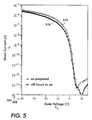
- FIG. 3shows the coalescence of the polymer blend allowing the formation of an insulating layer over the semiconducting layer.
- FIG. 4shows the finally separated thin film and the final polymer semiconductor protected by a polymer insulator in a bottom gate TFT.
- FIG. 5shows the transfer characteristic of a TFT formed from the described structure left in air.
- FIG. 6shows a top view of an electronic circuit that uses interconnect lines formed by segregating a semiconducting polymer from an insulating polymer.
- FIG. 7shows a side cross sectional view of the intersection between two intersecting interconnect lines.
- FIG. 8shows a diode including a semiconducting polymer and an electrode contact formed using a blended polymer.
- a method to process and encapsulate polymer electronicsis described herein.
- the methoduses a polymer blend that is composed of both a semiconducting and an insulating polymer. After deposition, the polymer blend segregates, to form a polymeric semiconducting layer encapsulated by the insulating polymer.
- An example where this method can be usedis to form polymer-based thin film transistors (TFT). Details of forming such a polymer TFT will be provided. However, many different devices may be formed using the described encapsulated semiconducting polymers, and the described invention should not be limited to any one device.
- FIG. 1shows a schematic of an example bottom gate polymeric TFT 100 .
- the illustrated TFTincludes a polymeric semiconducting layer 104 distributed between source 108 and drain 112 .
- Polymeric semiconductor 104is formed over a substrate, 116 .
- the substrateis a dielectric layer 116 .
- the substrateis formed over a gate line 120 .
- charge placed on the gate linecontrols the conductivity of polymeric semiconductor 104 .
- the charge on gate line 120controls current flow between drain 112 and source 108 .
- Dielectric layer 116 together with gate line 120form a base structure 124 .
- FIG. 2-5show a process of using a polymer blend solution to form a bottom gate polymeric TFT that includes an encapsulated polymer semiconductor.
- an encapsulation layer precipitated from the polymer blend solutionprotects polymeric semiconductor 104 .
- the polymer blend solutionincludes a semiconducting polymer and an insulating polymer.
- an insulating polymeris defined as a polymer that provides very high resistance to the passage of electric current. The insulating polymer and the semiconducting polymer are dissolved together in a common solvent.
- semiconducting polymerexamples include polythiophenes such as poly(3-alkylthiophene) (P3AT), poly(3-n-hexylthiophene) (P3HT) and poly[5,5′-bis(3-dodecyl-2-thienyl)-2,2′-bithiophene)(PQT-12) and polyfluorenes such as poly(fluorine-co-bithiophene) (F8T2) and poly(9,9′-dioctylfluorene-co-bis-N,N′-(4-butylphenyl)-bis-N,N′-phenyl-1,4-phenylenediamine) (TFB).
- P3ATpoly(3-alkylthiophene)
- P3HTpoly(3-n-hexylthiophene)
- PQT-12poly[5,5′-bis(3-dodecyl-2-thienyl
- Examples of typical insulating polymers that dissolve in solventsinclude poly(methyl methacrylate) (PMMA) and poly(4-vinylphenol) (PVP).
- Example of typical monomer that that become polymers when annealedinclude benzocyclobutene (BCB).
- Typical solvents that may be used to dissolve the semiconducting polymer and the insulating polymerare organic solvents such as dichlorobenzene, xylene, chloroform, mesitylene amongst others.
- the insulatormay be formed from a precursor material that becomes an insulator after an annealing or curing process.
- a precursor material that becomes a polymer semiconductor after an annealing or curing processmay be in lieu of an actual dissolved polymer.
- polymer dielectric filmscan be obtained from deposition of prepolymer, also know as polymer precursors.
- the solution of a polymer precursorcan contain monomers and oligomeners that when thermally treated, transforms into an insoluble polymer film.
- dielectric polymer obtained from deposition of precursorsare: polyimides which are synthesized from two monomers, a dianhydride and a diamine. Some variations of polyimides have been synthesized with structural modifications on the dianhydride and a diamine monomers, with the inclusion of flexible bridge monomers, fluorinated and silicone monomers, and acetylene terminated polyimides.
- a different class of dielectric polymerare the polybenzocyclobutenes (PBCB) derived from the monomer bisbenzocyclobutene (BCB). Thermal polymerization of BCB precursor occurs around 250 C in an oxygen-free environment.
- FIG. 2shows depositing polymer blend solution 204 onto a base structure that includes gate line 206 and substrate 208 .
- Polymer blend solution 204is deposited between source 212 and drain 216 .
- Source 212 and drain 216may be formed using a variety of techniques including photolithographic techniques, jet deposition and other techniques known to those of skill in the art.
- Semiconducting polymer and insulating polymerare dissolved in a solvent to form a uniform liquid polymer solution.
- the polymer solutiondoes not require heating and remains a liquid at room temperature (between 10 degrees and 50 degrees centigrade).
- Different techniquesmay be used to deposit the blended polymer solution 204 .
- deposition techniquesinclude spin coating, drop casting, ink jet printing and dip coating.
- the deposition method useddepends on several factors including the device to be fabricated and the viscosity of the polymer solution. For example, when jet printing the polymer solution, viscosity is typically maintained below 40 mPa.s and concentration of polymer/solvent may be adjusted to facilitate jetting conditions.
- spin coatinghigher concentration and higher viscosity polymer blend solutions may be used because film formation can be controlled by the spin coating speed and solvent evaporation rate.
- phase separationis defined as the process from which different polymer molecules dissolved in a common solvent are repealed and spontaneously separated from each other forming distinct domains, phases, of the different polymers.
- FIG. 3shows the polymer blend solution during a later stage of phase separation, often called coalescence stage.
- the coalescence stagemolecular mobility is reduced due to reduced amount of solvent, but distinct domains are still being formed.
- the composition and size of each domainis changing.
- the semiconducting polymer 304 in blended polymer solution 204exits the blended polymer solution.
- Low molecular mobility of polymer blend solution moleculescharacterizes the coalescence phase. Separation of polymer solution constituent components is carefully controlled. As will be described, several methods may be used to control the separation, including carefully selecting the characteristics of the substrate, the solvent, the semiconducting polymer and the insulating polymer to form the desired structure.
- One method of forming the structure of FIG. 3involves selecting the substrate 208 and polymer solution compounds based on the surface energy of the substrate 308 and polymer interactions with the substrate 308 .
- the substrate surface energy and the materialsare chosen so that the semiconducting polymer 304 has an affinity to the substrate resulting in better wettability conditions than that of the insulating material to the substrate.
- the insulating materialwould segregate to the top surface, forming a double layer structure.
- a substrate surface energy and an insulating materialmay be chosen such that the insulating material preferentially wets the semiconducting polymer and not to substrate 208 .
- ordering and formation of the polymer layersis partially controlled by wetting characteristics of one polymer to the other and wetting characteristics of each polymer to the substrate surface.
- the substrate surface energymay be modified.
- Techniques of modifying substrate surface energyinclude, but not limited to, plasma treatment, deposition of self assembled monolayer from solution, stamping of fluorinated hydrocarbon-terminated thiol or COOH-terminated thiol.
- the same end-terminated monolayercan be created with other attachment chemistries, including silylation-based monolayers.
- a third method of controlling double layer formationuses a combination of materials where the semiconducting polymer and an insulating material are selected such that the two polymers exhibit different solubility in the common solvent.
- the bottom layer material solubilityis lower than top layer material solubility.
- the bottom layer materialis semiconducting polymer 304 .
- Insulating polymer 308forms the top layer material. After deposition, the solute gradually evaporates causing the semiconducting polymer 304 to leave the solution before the higher solubility insulating polymer. When additional solvent evaporates, insulating polymer 308 also saturates and precipitates out of solution resulting in the formation of insulating polymer 308 over semiconducting polymer 304 .
- FIG. 4shows the bottom gate TFT after final separation of semiconducting polymer 404 from the insulating polymer 408 .
- the solventhas evaporated.
- the time it takes for the solvent to leave the filmis often called transformation time.
- the removal of the solvent from the polymer blendis controlled to maintain sufficient transformation time to enable full separation of the semiconducting polymer and the insulator.
- high boiling point solventsare often used.
- High boiling point solventshave slower solvent evaporation rate.
- Example solventsare organic solvents with boiling points in excess of 60 degrees centigrade. A typical solvent that fits those characteristics is dichlorobenzene. Typical solvent evaporation times are from one to six minutes after deposition.
- a second way of controlling evaporation rateis to create a solvent enriched atmosphere which slows down the solvent evaporation rate.
- One method of achieving a solvent rich atmosphereis to provide a solvent reservoir in a common sealed environment with the blend solution. Use of a solvent rich atmosphere is particularly well suited to spin coating and drop casting deposition methods.
- a film of semiconducting polymer 304remains in contact with dielectric layer 220 .
- the example illustrated structureis a bottom gate TFT.
- the semiconducting polymer filmacts as a switch that controls current flow between source 212 and drain 216 according to a voltage applied to gate line 224 .
- Polymeric semiconductorsusually behave as a p type semiconductor.
- the semiconducting polymer filmprevents the flow of current between source 212 and drain 216 .
- the p type semiconducting polymer filmallows current to flow between source 212 and drain 216 .
- insulating polymer 408encapsulates the semiconducting polymer 404 minimizing device degradation by reducing environmental exposure. The encapsulation improves the long term performance of the semiconducting polymer and also allows further devices to be deposited over the gate region of the thin film transistor.
- FIG. 5shows an approximate transfer characteristic of a TFT of the type shown in FIG. 4 .
- the drain currentis provided on a vertical axis 504 and the gate voltage is shown along horizontal axis 508 .
- a first plot 512shows the transfer characteristic immediately after fabrication and a second plot 516 shows the device characteristic 2 days after fabrication. As can be seen, the similar performance shows minimal changes after two days suggesting that the insulating polymer effectively minimizes degradation of the semiconducting polymer by encapsulating the semiconducting polymer.
- a polymer blend to create an insulating layer that encapsulates a circuit elementmay be used in a variety of electronic devices.
- the encapsulationmay be used to environmentally isolate the circuit element as previously described or the encapsulation may be used to electrically isolate the circuit element to allow for circuit element stacking.
- an insulatormay be blended with a conducting polymer or with a metal colloidal dispersion to form a double layer film.
- the double layer filmincludes a conducting layer and a non-conducting layer.
- FIG. 6shows using a conducting and non-conducting blend to fabricate stacked interconnecting lines.
- the non-conducting layer of the double layerseparates stacked interconnect lines preventing a short circuit.
- conductor/insulator blendscan also be used to form the top contact of diodes. Typical diodes include light emitting diodes, rectifying diodes and photodiodes.
- FIG. 8shows an example of using an insulator and a conductor blend to form a diode top contact.
- a blend solution of a conducting and an insulating polymerforms interconnect lines between circuit elements.
- the conducting linessuch as line 604 and line 608 interconnect circuit devices, such as circuit devices 612 , 616 , 620 .
- the circuit devices 612 , 616 , 620are thin film transistors for use in a display system, although such an array of thin film transistors may also be commonly used in a sensor system.
- One method of forming the structure of FIG. 6uses a droplet ejection mechanism, such as a jet printer or a piezo-electric print mechanism, to eject droplets of the blend solution. After ejection, the conductor and the insulating polymer segregate. A solvent that carries the conductor and the insulator evaporates leaving behind the conductor overlayed by the insulator. As in the case of a semiconducting and insulating blend solution previously described, several techniques may be used to make sure that the insulator overlays the conductor. Those techniques include selecting a substrate that preferentially wets to the conductor, selecting an insulator that preferentially wets to the conductor or selecting a conductor that has a lower solubility in the solvent than the insulator.
- a droplet ejection mechanismsuch as a jet printer or a piezo-electric print mechanism
- Example conductor materialsinclude poly(3,4-ethylene dioxy thiophene) doped with polystyrene sulfonic acid (PEDOT/PSS), polyaniline (PANI), metal nanoparticles (Au, Ag), carbon nanotubes.
- Example insulating polymers previously identifiedinclude poly-(methyl methacrylate) (PMMA), poly(4-vinylphenol) (PVP) and benzocyclobutene (BCB).
- Typical solventspreviously identified include organic solvents such as dichlorobenzene, xylene, chloroform, and mesitylene amongst others.
- the conductorforms a conducting line such as line 604 and line 608 connecting electronic devices.
- the conducting linesmay couple sources, drains, and gates of the transistors to a power source, or to a circuit that controls the display.
- An insulating polymer layercovers and insulates each conducting lines. The insulating polymer protects conducting lines 604 and 608 from environmental damage. The insulating polymer also allows other electronic devices stacked over conducting lines 604 , 608 , including intersecting conducting lines 624 , 628 from short circuiting or otherwise interfering with the current carried in lines 604 , 608 .
- FIG. 7shows a cross sectional side view of an example intersection of conducting lines such as intersection 650 of FIG. 6 .
- First deposited conducting line 604includes an insulating layer 712 overlying a conducting layer 708 . Insulating layer 712 allows electrical devices to be deposited over the conducting line 604 .
- the electrical deviceis another conducting line 654 . Conducting line 654 runs perpendicular to conducting line 604 .
- conducting line 654is deposited after the solvent that carried insulating layer 712 has evaporated.
- conducting line 654is also printed with a polymer blend including a solvent, a conductor and an insulator.
- the solvent usedis carefully selected so as not to dissolve previously deposited layers, in particular the solvent should not dissolve insulator 712 .
- typical solventsincluding water and alcohol based solvents.
- the bottom insulatormay be formed from a precursor that is crosslinked during annealing such that it will not dissolve upon exposure to later deposited solvents.
- the polymer blendforms conducting layer 716 .
- Insulating material dissolved in the polymer blend solutionforms an insulating layer 720 over the conducting layer.
- the insulating layerseals conducting layer 716 from environmental damage and also permits subsequent electronic devices to be deposited over conducting line 654 .
- FIG. 8shows still another use of a conductor/insulator blend of polymer material.
- a blend solutionis used to form an electrical contact to a diode.
- the diodeis a light emitting diode.
- a first conductor 804is deposited over a substrate 800 .
- First conductor 804may be a metal such as aluminum or copper.
- a semiconductor 808 deposited over first electrode 804forms the active region of the diode. The semiconductor outputs lights through a facet, such as facet 808 , when electrical energy is injected into the semiconductor.
- a second electrical contact or electrode 812is formed over semiconductor 808 .
- the second electrical contactis deposited in a polymer blend solution that includes a conducting material, an insulating material and a solvent. As the solvent evaporates, the conducting material and insulator segregate and exit solution.
- the conducting materialforms electrode 812 .
- the insulating materialforms a protective layer 815 .
Landscapes
- Engineering & Computer Science (AREA)
- Chemical & Material Sciences (AREA)
- Nanotechnology (AREA)
- Physics & Mathematics (AREA)
- Crystallography & Structural Chemistry (AREA)
- Materials Engineering (AREA)
- General Physics & Mathematics (AREA)
- Condensed Matter Physics & Semiconductors (AREA)
- Composite Materials (AREA)
- Mathematical Physics (AREA)
- Theoretical Computer Science (AREA)
- Manufacturing & Machinery (AREA)
- Thin Film Transistor (AREA)
- Electroluminescent Light Sources (AREA)
- Formation Of Insulating Films (AREA)
Abstract
Description
- This application is related to patent application Ser. No. ______ (attorney docket number 20031723Q-US-NP entitled “Improved Method for Interconnecting Electronic Components Using a Blend Solution to Form a Conducting Layer and an Insulating Layer” by the Same Inventor and filed on the same date.
- Polymer based electronic devices represent an alternative to conventional inorganic based devices due to recent advances in polymer synthesis and polymer based device performance. These advances include high luminescence efficiency in polymer light emitting diodes (LEDs) and improved field effect mobilities in polymeric thin film transistors (TFTs). However, the environmental instability of polymer based electronic devices remains a commercial barrier.
- Oxygen, humidity, light and heat amongst other environmental parameters, can damage polymeric materials. To minimize material degradation, polymer based electronic devices are often fabricated and tested under tightly controlled environmental conditions, typically in a “glove box” filled with an inert gas, or under vacuum conditions. Large scale fabrication under tightly controlled environments increases the cost of fabrication reducing commercialization opportunities.
- Encapsulation of semiconducting and conducting polymers in fabricated devices minimizes environmental exposure and thus device degradation after fabrication. However, encapsulating polymeric layers is difficult because of polymeric layer incompatibility with the processes used in encapsulation. Many materials available for encapsulation utilize process steps that involve high temperatures or solvents that may damage the polymeric semiconductor. Light used when depositing solid encapsulating layers can also damage the polymeric layers.
- Thus an improved non-destructive method for forming and encapsulating polymeric layers in electronic devices is needed.
- A method of forming a bottom gate thin film transistor is described. In the method, a source and a drain are formed over regions of a substrate. A blend solution including a material designed to form a semiconductor polymer and a material designed to form an insulator are deposited between the source and the drain such that the semiconducting polymer forms a layer between the source and drain of the bottom gate transistor.
FIG. 1 shows one example of a bottom gate thin film transistor.FIG. 2 shows the first step in forming the structure ofFIG. 1 using a polymer blend in a liquid phase.FIG. 3 shows the coalescence of the polymer blend allowing the formation of an insulating layer over the semiconducting layer.FIG. 4 shows the finally separated thin film and the final polymer semiconductor protected by a polymer insulator in a bottom gate TFT.FIG. 5 shows the transfer characteristic of a TFT formed from the described structure left in air.FIG. 6 shows a top view of an electronic circuit that uses interconnect lines formed by segregating a semiconducting polymer from an insulating polymer.FIG. 7 shows a side cross sectional view of the intersection between two intersecting interconnect lines.FIG. 8 shows a diode including a semiconducting polymer and an electrode contact formed using a blended polymer.- A method to process and encapsulate polymer electronics is described herein. The method uses a polymer blend that is composed of both a semiconducting and an insulating polymer. After deposition, the polymer blend segregates, to form a polymeric semiconducting layer encapsulated by the insulating polymer. An example where this method can be used is to form polymer-based thin film transistors (TFT). Details of forming such a polymer TFT will be provided. However, many different devices may be formed using the described encapsulated semiconducting polymers, and the described invention should not be limited to any one device.
FIG. 1 shows a schematic of an example bottom gatepolymeric TFT 100. The illustrated TFT includes a polymericsemiconducting layer 104 distributed betweensource 108 anddrain 112.Polymeric semiconductor 104 is formed over a substrate,116. In the illustration, the substrate is adielectric layer 116. The substrate is formed over a gate line120. During operation, charge placed on the gate line controls the conductivity ofpolymeric semiconductor 104. Thus the charge on gate line120 controls current flow betweendrain 112 andsource 108.Dielectric layer 116 together with gate line120 form abase structure 124.FIG. 2-5 show a process of using a polymer blend solution to form a bottom gate polymeric TFT that includes an encapsulated polymer semiconductor. In the final structure, an encapsulation layer precipitated from the polymer blend solution protectspolymeric semiconductor 104. In one embodiment, the polymer blend solution includes a semiconducting polymer and an insulating polymer. As used herein, an insulating polymer is defined as a polymer that provides very high resistance to the passage of electric current. The insulating polymer and the semiconducting polymer are dissolved together in a common solvent.- Many different polymers may be used for the semiconducting polymer and insulating polymer. Examples of typical semiconducting polymers include polythiophenes such as poly(3-alkylthiophene) (P3AT), poly(3-n-hexylthiophene) (P3HT) and poly[5,5′-bis(3-dodecyl-2-thienyl)-2,2′-bithiophene)(PQT-12) and polyfluorenes such as poly(fluorine-co-bithiophene) (F8T2) and poly(9,9′-dioctylfluorene-co-bis-N,N′-(4-butylphenyl)-bis-N,N′-phenyl-1,4-phenylenediamine) (TFB). Examples of typical insulating polymers that dissolve in solvents include poly(methyl methacrylate) (PMMA) and poly(4-vinylphenol) (PVP). Example of typical monomer that that become polymers when annealed (hereinafter polymer precursors) include benzocyclobutene (BCB). Typical solvents that may be used to dissolve the semiconducting polymer and the insulating polymer are organic solvents such as dichlorobenzene, xylene, chloroform, mesitylene amongst others.
- In an alternate embodiment, other materials may be substituted for the polymer insulator and polymer conductor. For example, the insulator may be formed from a precursor material that becomes an insulator after an annealing or curing process. Likewise, a precursor material that becomes a polymer semiconductor after an annealing or curing process may be in lieu of an actual dissolved polymer. In particular, polymer dielectric films can be obtained from deposition of prepolymer, also know as polymer precursors. The solution of a polymer precursor can contain monomers and oligomeners that when thermally treated, transforms into an insoluble polymer film. Examples of dielectric polymer obtained from deposition of precursors (amongst others) are: polyimides which are synthesized from two monomers, a dianhydride and a diamine. Some variations of polyimides have been synthesized with structural modifications on the dianhydride and a diamine monomers, with the inclusion of flexible bridge monomers, fluorinated and silicone monomers, and acetylene terminated polyimides. A different class of dielectric polymer are the polybenzocyclobutenes (PBCB) derived from the monomer bisbenzocyclobutene (BCB). Thermal polymerization of BCB precursor occurs around 250 C in an oxygen-free environment.
FIG. 2 shows depositingpolymer blend solution 204 onto a base structure that includesgate line 206 andsubstrate 208.Polymer blend solution 204 is deposited betweensource 212 and drain216.Source 212 anddrain 216 may be formed using a variety of techniques including photolithographic techniques, jet deposition and other techniques known to those of skill in the art. During deposition, semiconducting polymer and insulating polymer are dissolved in a solvent to form a uniform liquid polymer solution. Typically, the polymer solution does not require heating and remains a liquid at room temperature (between 10 degrees and 50 degrees centigrade).- Different techniques may be used to deposit the blended
polymer solution 204. Examples of deposition techniques include spin coating, drop casting, ink jet printing and dip coating. The deposition method used depends on several factors including the device to be fabricated and the viscosity of the polymer solution. For example, when jet printing the polymer solution, viscosity is typically maintained below 40 mPa.s and concentration of polymer/solvent may be adjusted to facilitate jetting conditions. When spin coating, higher concentration and higher viscosity polymer blend solutions may be used because film formation can be controlled by the spin coating speed and solvent evaporation rate. - Immediately after deposition but prior to solvent evaporation, the polymer blend solution is rich in solvent, and the molecules are highly mobile. This solution stage is often called the diffusion and liquid flow regime. The liquid flow regime is characterized by high molecular mobility of molecules in a blended polymer solution. The first stages of phase separation between the semiconducting polymer and the insulator occurs during the liquid flow regime. As used herein, phase separation is defined as the process from which different polymer molecules dissolved in a common solvent are repealed and spontaneously separated from each other forming distinct domains, phases, of the different polymers.
FIG. 3 shows the polymer blend solution during a later stage of phase separation, often called coalescence stage. In the coalescence stage, molecular mobility is reduced due to reduced amount of solvent, but distinct domains are still being formed. At this stage, the composition and size of each domain is changing. InFIG. 3 thesemiconducting polymer 304 in blendedpolymer solution 204 exits the blended polymer solution. Low molecular mobility of polymer blend solution molecules characterizes the coalescence phase. Separation of polymer solution constituent components is carefully controlled. As will be described, several methods may be used to control the separation, including carefully selecting the characteristics of the substrate, the solvent, the semiconducting polymer and the insulating polymer to form the desired structure.- One method of forming the structure of
FIG. 3 involves selecting thesubstrate 208 and polymer solution compounds based on the surface energy of thesubstrate 308 and polymer interactions with thesubstrate 308. In particular, the substrate surface energy and the materials are chosen so that thesemiconducting polymer 304 has an affinity to the substrate resulting in better wettability conditions than that of the insulating material to the substrate. In the described example, the insulating material would segregate to the top surface, forming a double layer structure. Alternatively, a substrate surface energy and an insulating material may be chosen such that the insulating material preferentially wets the semiconducting polymer and not tosubstrate 208. Thus ordering and formation of the polymer layers is partially controlled by wetting characteristics of one polymer to the other and wetting characteristics of each polymer to the substrate surface. - Different techniques may be used to adjust the interaction between polymers and between polymer and substrate. In order to adjust the interaction between substrate and polymer, the substrate surface energy may be modified. Techniques of modifying substrate surface energy include, but not limited to, plasma treatment, deposition of self assembled monolayer from solution, stamping of fluorinated hydrocarbon-terminated thiol or COOH-terminated thiol. The same end-terminated monolayer can be created with other attachment chemistries, including silylation-based monolayers.
- A third method of controlling double layer formation uses a combination of materials where the semiconducting polymer and an insulating material are selected such that the two polymers exhibit different solubility in the common solvent. In the present example the bottom layer material solubility is lower than top layer material solubility. In the illustrated example, the bottom layer material is
semiconducting polymer 304. Insulatingpolymer 308 forms the top layer material. After deposition, the solute gradually evaporates causing thesemiconducting polymer 304 to leave the solution before the higher solubility insulating polymer. When additional solvent evaporates, insulatingpolymer 308 also saturates and precipitates out of solution resulting in the formation of insulatingpolymer 308 oversemiconducting polymer 304. FIG. 4 shows the bottom gate TFT after final separation ofsemiconducting polymer 404 from the insulatingpolymer 408. InFIG. 4 , the solvent has evaporated. The time it takes for the solvent to leave the film is often called transformation time. The removal of the solvent from the polymer blend is controlled to maintain sufficient transformation time to enable full separation of the semiconducting polymer and the insulator. In order to extend the time in the diffusion and liquid flow regime, high boiling point solvents are often used. High boiling point solvents have slower solvent evaporation rate. Example solvents are organic solvents with boiling points in excess of 60 degrees centigrade. A typical solvent that fits those characteristics is dichlorobenzene. Typical solvent evaporation times are from one to six minutes after deposition.- The transformation time can also be increased by altering processing techniques; thus the use of the method described is not limited to high boiling point solvents. A second way of controlling evaporation rate is to create a solvent enriched atmosphere which slows down the solvent evaporation rate. One method of achieving a solvent rich atmosphere is to provide a solvent reservoir in a common sealed environment with the blend solution. Use of a solvent rich atmosphere is particularly well suited to spin coating and drop casting deposition methods.
- After solvent evaporation, a film of
semiconducting polymer 304 remains in contact with dielectric layer220. The example illustrated structure is a bottom gate TFT. In a TFT, the semiconducting polymer film acts as a switch that controls current flow betweensource 212 and drain216 according to a voltage applied to gate line224. Polymeric semiconductors usually behave as a p type semiconductor. In a P type semiconducting polymer film, when no voltage is applied to gate line224, the semiconducting polymer film prevents the flow of current betweensource 212 and drain216. When a voltage is applied to gate line224, the p type semiconducting polymer film allows current to flow betweensource 212 and drain216. - In
FIG. 4 , insulatingpolymer 408 encapsulates thesemiconducting polymer 404 minimizing device degradation by reducing environmental exposure. The encapsulation improves the long term performance of the semiconducting polymer and also allows further devices to be deposited over the gate region of the thin film transistor. FIG. 5 shows an approximate transfer characteristic of a TFT of the type shown inFIG. 4 . The drain current is provided on avertical axis 504 and the gate voltage is shown alonghorizontal axis 508. Afirst plot 512 shows the transfer characteristic immediately after fabrication and asecond plot 516 shows the device characteristic 2 days after fabrication. As can be seen, the similar performance shows minimal changes after two days suggesting that the insulating polymer effectively minimizes degradation of the semiconducting polymer by encapsulating the semiconducting polymer.- Although the preceding description has been provided in terms of a TFT, the use of a polymer blend to create an insulating layer that encapsulates a circuit element may be used in a variety of electronic devices. The encapsulation may be used to environmentally isolate the circuit element as previously described or the encapsulation may be used to electrically isolate the circuit element to allow for circuit element stacking. For example, an insulator may be blended with a conducting polymer or with a metal colloidal dispersion to form a double layer film. The double layer film includes a conducting layer and a non-conducting layer.
FIG. 6 shows using a conducting and non-conducting blend to fabricate stacked interconnecting lines. InFIG. 6 , the non-conducting layer of the double layer separates stacked interconnect lines preventing a short circuit. In an alternate embodiment, conductor/insulator blends can also be used to form the top contact of diodes. Typical diodes include light emitting diodes, rectifying diodes and photodiodes.FIG. 8 shows an example of using an insulator and a conductor blend to form a diode top contact. - In the embodiment shown in
FIG. 6 , a blend solution of a conducting and an insulating polymer forms interconnect lines between circuit elements. The conducting lines such asline 604 andline 608 interconnect circuit devices, such ascircuit devices FIG. 6 , thecircuit devices - One method of forming the structure of
FIG. 6 uses a droplet ejection mechanism, such as a jet printer or a piezo-electric print mechanism, to eject droplets of the blend solution. After ejection, the conductor and the insulating polymer segregate. A solvent that carries the conductor and the insulator evaporates leaving behind the conductor overlayed by the insulator. As in the case of a semiconducting and insulating blend solution previously described, several techniques may be used to make sure that the insulator overlays the conductor. Those techniques include selecting a substrate that preferentially wets to the conductor, selecting an insulator that preferentially wets to the conductor or selecting a conductor that has a lower solubility in the solvent than the insulator. - Many different compounds may be used for the conductor, insulating polymer and solvent. Example conductor materials include poly(3,4-ethylene dioxy thiophene) doped with polystyrene sulfonic acid (PEDOT/PSS), polyaniline (PANI), metal nanoparticles (Au, Ag), carbon nanotubes. Example insulating polymers previously identified include poly-(methyl methacrylate) (PMMA), poly(4-vinylphenol) (PVP) and benzocyclobutene (BCB). Typical solvents previously identified include organic solvents such as dichlorobenzene, xylene, chloroform, and mesitylene amongst others.
- As the solvent evaporates, the conductor forms a conducting line such as
line 604 andline 608 connecting electronic devices. When the electronic devices are transistors in a display, the conducting lines may couple sources, drains, and gates of the transistors to a power source, or to a circuit that controls the display. An insulating polymer layer covers and insulates each conducting lines. The insulating polymer protects conductinglines lines intersecting conducting lines lines FIG. 7 shows a cross sectional side view of an example intersection of conducting lines such asintersection 650 ofFIG. 6 . First deposited conductingline 604 includes an insulatinglayer 712 overlying aconducting layer 708. Insulatinglayer 712 allows electrical devices to be deposited over the conductingline 604. In the example ofFIG. 7 , “the electrical device” is another conducting line654. Conducting line654 runs perpendicular to conductingline 604.- During formation, conducting line654 is deposited after the solvent that carried insulating
layer 712 has evaporated. Typically, conducting line654 is also printed with a polymer blend including a solvent, a conductor and an insulator. The solvent used is carefully selected so as not to dissolve previously deposited layers, in particular the solvent should not dissolveinsulator 712. Examples of typical solvents including water and alcohol based solvents. Alternately the bottom insulator may be formed from a precursor that is crosslinked during annealing such that it will not dissolve upon exposure to later deposited solvents. - As the solvent evaporates, the polymer blend
forms conducting layer 716. Insulating material dissolved in the polymer blend solution forms an insulatinglayer 720 over the conducting layer. The insulating layerseals conducting layer 716 from environmental damage and also permits subsequent electronic devices to be deposited over conducting line654. FIG. 8 shows still another use of a conductor/insulator blend of polymer material. InFIG. 8 , a blend solution is used to form an electrical contact to a diode. In one embodiment, the diode is a light emitting diode.- In
FIG. 8 , afirst conductor 804 is deposited over asubstrate 800.First conductor 804 may be a metal such as aluminum or copper. Asemiconductor 808 deposited overfirst electrode 804 forms the active region of the diode. The semiconductor outputs lights through a facet, such asfacet 808, when electrical energy is injected into the semiconductor. - A second electrical contact or
electrode 812 is formed oversemiconductor 808. The second electrical contact is deposited in a polymer blend solution that includes a conducting material, an insulating material and a solvent. As the solvent evaporates, the conducting material and insulator segregate and exit solution. The conducting material forms electrode812. The insulating material forms aprotective layer 815. Bycoupling electrode 812 andfirst conductor 804 to a power source,semiconductor 808 can be electrically excited to output light. - Many of the presented details are designed to provide examples and facilitate understanding of the invention and various ways the invention can be used. Such details are not meant to, and should not be interpreted to limit the claims. For example, although most of the specification describes how to fabricate a thin film transistor using the described techniques, a large variety of electronic components can be formed using the described technique. Thus the inventions should not be limited by these examples, but only by the claims as presented, the amendments to the claims, and variations, alternatives, modifications, improvements, equivalents, and substantial equivalents of the embodiments described in the claims.
Claims (28)
Priority Applications (3)
| Application Number | Priority Date | Filing Date | Title |
|---|---|---|---|
| US10/876,229US7351606B2 (en) | 2004-06-24 | 2004-06-24 | Method for forming a bottom gate thin film transistor using a blend solution to form a semiconducting layer and an insulating layer |
| JP2005178743AJP5102946B2 (en) | 2004-06-24 | 2005-06-20 | Improved method of forming bottom-gate thin film transistors using mixed solutions to form semiconductor and insulating layers |
| CN2005100794793ACN1722388B (en) | 2004-06-24 | 2005-06-23 | Method for forming a bottom gate thin film transistor using a blend solution to form a semiconducting layer and an insulating layer |
Applications Claiming Priority (1)
| Application Number | Priority Date | Filing Date | Title |
|---|---|---|---|
| US10/876,229US7351606B2 (en) | 2004-06-24 | 2004-06-24 | Method for forming a bottom gate thin film transistor using a blend solution to form a semiconducting layer and an insulating layer |
Publications (2)
| Publication Number | Publication Date |
|---|---|
| US20050287728A1true US20050287728A1 (en) | 2005-12-29 |
| US7351606B2 US7351606B2 (en) | 2008-04-01 |
Family
ID=35506401
Family Applications (1)
| Application Number | Title | Priority Date | Filing Date |
|---|---|---|---|
| US10/876,229Expired - LifetimeUS7351606B2 (en) | 2004-06-24 | 2004-06-24 | Method for forming a bottom gate thin film transistor using a blend solution to form a semiconducting layer and an insulating layer |
Country Status (3)
| Country | Link |
|---|---|
| US (1) | US7351606B2 (en) |
| JP (1) | JP5102946B2 (en) |
| CN (1) | CN1722388B (en) |
Cited By (12)
| Publication number | Priority date | Publication date | Assignee | Title |
|---|---|---|---|---|
| US20050287781A1 (en)* | 2004-06-24 | 2005-12-29 | Palo Alto Research Center Incorporated | Method for interconnecting electronic components using a blend solution to from a conducting layer and an insulating layer |
| US20060273302A1 (en)* | 2005-06-06 | 2006-12-07 | Xerox Corporation | Barrier layer for an organic electronic device |
| US20070145357A1 (en)* | 2005-12-23 | 2007-06-28 | Xerox Corporation | Thin-film transistor |
| US7351606B2 (en) | 2004-06-24 | 2008-04-01 | Palo Alto Research Center Incorporated | Method for forming a bottom gate thin film transistor using a blend solution to form a semiconducting layer and an insulating layer |
| US20090155994A1 (en)* | 2007-12-12 | 2009-06-18 | Hawkins Gilbert A | Forming thin film transistors using ablative films with pre-patterned conductors |
| US20100270542A1 (en)* | 2007-12-17 | 2010-10-28 | Peiwang Zhu | Solution Processable Organic Semiconductors |
| EP2377179A4 (en)* | 2008-12-18 | 2013-08-07 | Postech Acad Ind Found | METHOD FOR MANUFACTURING MULTILAYER THIN FILM BY PHASE SEPARATION OF THE ORGANIC / INSULATING SEMICONDUCTOR POLYMER MIXTURE AND ORGANIC THIN FILM TRANSISTOR USING THE SAME |
| WO2014038132A1 (en)* | 2012-09-10 | 2014-03-13 | Sony Corporation | Method of manufacturing semiconductor device, semiconductor device, and electronic apparatus |
| EP2036141B1 (en)* | 2006-06-29 | 2015-09-30 | Cambridge Enterprise Limited | Blended polymer fets |
| CN112858801A (en)* | 2021-01-08 | 2021-05-28 | 青岛科技大学 | Method and system for reducing space charge injection under direct-current high electric field |
| US20210202245A1 (en)* | 2019-12-27 | 2021-07-01 | Kokusai Electric Corporation | Method of manufacturing semiconductor device, substrate processing apparatus, and recording medium |
| US11923193B2 (en) | 2020-02-27 | 2024-03-05 | Kokusai Electric Corporation | Method of manufacturing semiconductor device, substrate processing apparatus, and recording medium |
Families Citing this family (19)
| Publication number | Priority date | Publication date | Assignee | Title |
|---|---|---|---|---|
| DE10340643B4 (en)* | 2003-09-03 | 2009-04-16 | Polyic Gmbh & Co. Kg | Printing method for producing a double layer for polymer electronics circuits, and thereby produced electronic component with double layer |
| TWI228833B (en)* | 2004-05-04 | 2005-03-01 | Ind Tech Res Inst | Method for enhancing the electrical characteristics of organic electronic devices |
| GB0410921D0 (en)* | 2004-05-14 | 2004-06-16 | Plastic Logic Ltd | Self-aligned active layer island |
| US7615483B2 (en)* | 2006-12-22 | 2009-11-10 | Palo Alto Research Center Incorporated | Printed metal mask for UV, e-beam, ion-beam and X-ray patterning |
| US7687577B2 (en)* | 2007-07-25 | 2010-03-30 | Sabic Innovative Plastics Ip B.V. | Thermoformable polycarbonate/polyester compositions and uses |
| JP5126508B2 (en)* | 2008-03-25 | 2013-01-23 | Jsr株式会社 | Insulating film forming composition, insulating film manufacturing method, and insulating film obtained thereby |
| JP5403204B2 (en)* | 2008-03-25 | 2014-01-29 | Jsr株式会社 | Insulating film forming composition, insulating film manufacturing method, and insulating film obtained thereby |
| JP2009277710A (en)* | 2008-05-12 | 2009-11-26 | Ricoh Co Ltd | Organic transistor, method of manufacturing organic transistor, organic transistor array, and display device |
| KR101561322B1 (en)* | 2008-07-02 | 2015-10-16 | 바스프 에스이 | High performance solution processable semiconducting polymers based on alternating donor acceptor copolymers |
| KR20100031036A (en)* | 2008-09-11 | 2010-03-19 | 포항공과대학교 산학협력단 | A manufacturing method of a thin film organic semiconductor using a phase seperation of blend of organic semiconductor/insulating polymer and organic thin film transister |
| KR101376494B1 (en)* | 2008-12-18 | 2014-03-19 | 포항공과대학교 산학협력단 | Fabricating low-cost polymer thin-film transistors via formation of semiconducting nanofibrillar network in semiconducting/insulating polymer blends |
| WO2014162287A2 (en) | 2013-04-06 | 2014-10-09 | Indian Institute Of Technology Kanpur | Organic thin film transistors and methods for their manufacturing and use |
| US9356248B2 (en) | 2013-08-16 | 2016-05-31 | Palo Alto Research Center Incorporated | Organic thin-film transistor |
| JP5715664B2 (en)* | 2013-08-21 | 2015-05-13 | 日本化薬株式会社 | Organic semiconductor composition |
| WO2016031968A1 (en)* | 2014-08-29 | 2016-03-03 | 国立大学法人東京大学 | Fabrication method of semiconductor film, semiconductor film, and field effect transistor |
| JP6298896B2 (en)* | 2014-09-29 | 2018-03-20 | 富士フイルム株式会社 | Organic semiconductor film manufacturing method, organic transistor |
| US9853230B2 (en) | 2015-02-17 | 2017-12-26 | Xerox Corporation | Printable nanoparticle conductor ink with improved charge injection |
| US10741766B2 (en) | 2016-05-12 | 2020-08-11 | Samsung Electronics Co., Ltd. | Organic semiconductor thin film and method of manufacturing the same and thin film transistor and electronic device |
| CN109841735B (en)* | 2017-09-30 | 2020-11-06 | Tcl科技集团股份有限公司 | Preparation method of TFT, ink for preparing TFT and preparation method thereof |
Citations (17)
| Publication number | Priority date | Publication date | Assignee | Title |
|---|---|---|---|---|
| US3683396A (en)* | 1970-08-05 | 1972-08-08 | Dick Co Ab | Method and apparatus for control of ink drop formation |
| US5213715A (en)* | 1989-04-17 | 1993-05-25 | Western Digital Corporation | Directionally conductive polymer |
| US5872205A (en)* | 1995-08-30 | 1999-02-16 | Balke; Stephen Thomas | Polymer segregation process |
| US6107117A (en)* | 1996-12-20 | 2000-08-22 | Lucent Technologies Inc. | Method of making an organic thin film transistor |
| US6326936B1 (en)* | 1997-07-22 | 2001-12-04 | Thin Film Electronics Asa | Electrode means, comprising polymer materials, with or without functional elements and an electrode device formed of said means |
| US6359672B2 (en)* | 1997-10-20 | 2002-03-19 | Guardian Industries Corp. | Method of making an LCD or X-ray imaging device with first and second insulating layers |
| US20020040805A1 (en)* | 2000-02-04 | 2002-04-11 | Swager Timothy M. | Insulated nanoscopic pathways, compositions and devices of the same |
| US20020119584A1 (en)* | 1999-07-21 | 2002-08-29 | E Ink Corporation | Preferred methods for producing electrical circuit elements used to control an electronic display |
| US6503831B2 (en)* | 1997-10-14 | 2003-01-07 | Patterning Technologies Limited | Method of forming an electronic device |
| US20030071246A1 (en)* | 2001-01-23 | 2003-04-17 | Grigorov Leonid N. | Quantum devices based on crystallized electron pairs and methods for their manufacture and use |
| US20030138566A1 (en)* | 2000-07-05 | 2003-07-24 | Adam Pron | Method for preparing conductive composite materials by deposition of a conductive polymer in an insulating porous substrate and solution for use in said preparation |
| US20030157244A1 (en)* | 2001-04-03 | 2003-08-21 | Takeo Kawase | Patterning method |
| US20030161959A1 (en)* | 2001-11-02 | 2003-08-28 | Kodas Toivo T. | Precursor compositions for the deposition of passive electronic features |
| US20040227891A1 (en)* | 2003-05-14 | 2004-11-18 | Naoto Hirota | High quality and ultra large screen liquid crystal display device and production method thereof |
| US20050045855A1 (en)* | 2003-09-03 | 2005-03-03 | Tonapi Sandeep Shrikant | Thermal conductive material utilizing electrically conductive nanoparticles |
| US20050078099A1 (en)* | 2002-04-24 | 2005-04-14 | E Ink Corporation | Electro-optic displays, and components for use therein |
| US20050151820A1 (en)* | 2001-12-21 | 2005-07-14 | Henning Sirringhaus | Self-aligned printing |
Family Cites Families (8)
| Publication number | Priority date | Publication date | Assignee | Title |
|---|---|---|---|---|
| JPH01234435A (en) | 1988-03-16 | 1989-09-19 | Inoue Mtp Co Ltd | Electrically conductive polymer composite and production thereof |
| JP2813428B2 (en)* | 1989-08-17 | 1998-10-22 | 三菱電機株式会社 | Field effect transistor and liquid crystal display device using the field effect transistor |
| JPH07336752A (en)* | 1994-06-10 | 1995-12-22 | Fujitsu Ltd | Group selection control method for mobile terminals |
| FR2732501B1 (en) | 1995-03-28 | 1997-04-30 | Commissariat Energie Atomique | METHOD FOR MANUFACTURING MATERIALS WITH IMPROVED DIELECTRIC RIGIDITY, AND USE OF THE MATERIALS OBTAINED BY THIS PROCESS IN THE MANUFACTURE OF ENERGY TRANSPORT CABLES |
| CN1149606C (en)* | 2001-03-13 | 2004-05-12 | 华南理工大学 | A field emission cathode |
| JP4439292B2 (en)* | 2004-02-24 | 2010-03-24 | シャープ株式会社 | ORGANIC TRANSISTOR, ITS MANUFACTURING METHOD, AND ORGANIC TRANSISTOR MANUFACTURING DEVICE |
| JP2005243822A (en)* | 2004-02-25 | 2005-09-08 | Seiko Epson Corp | Thin film transistor manufacturing method, thin film transistor, thin film transistor circuit, electronic device and electronic apparatus |
| US7351606B2 (en) | 2004-06-24 | 2008-04-01 | Palo Alto Research Center Incorporated | Method for forming a bottom gate thin film transistor using a blend solution to form a semiconducting layer and an insulating layer |
- 2004
- 2004-06-24USUS10/876,229patent/US7351606B2/ennot_activeExpired - Lifetime
- 2005
- 2005-06-20JPJP2005178743Apatent/JP5102946B2/ennot_activeExpired - Fee Related
- 2005-06-23CNCN2005100794793Apatent/CN1722388B/ennot_activeExpired - Fee Related
Patent Citations (17)
| Publication number | Priority date | Publication date | Assignee | Title |
|---|---|---|---|---|
| US3683396A (en)* | 1970-08-05 | 1972-08-08 | Dick Co Ab | Method and apparatus for control of ink drop formation |
| US5213715A (en)* | 1989-04-17 | 1993-05-25 | Western Digital Corporation | Directionally conductive polymer |
| US5872205A (en)* | 1995-08-30 | 1999-02-16 | Balke; Stephen Thomas | Polymer segregation process |
| US6107117A (en)* | 1996-12-20 | 2000-08-22 | Lucent Technologies Inc. | Method of making an organic thin film transistor |
| US6326936B1 (en)* | 1997-07-22 | 2001-12-04 | Thin Film Electronics Asa | Electrode means, comprising polymer materials, with or without functional elements and an electrode device formed of said means |
| US6503831B2 (en)* | 1997-10-14 | 2003-01-07 | Patterning Technologies Limited | Method of forming an electronic device |
| US6359672B2 (en)* | 1997-10-20 | 2002-03-19 | Guardian Industries Corp. | Method of making an LCD or X-ray imaging device with first and second insulating layers |
| US20020119584A1 (en)* | 1999-07-21 | 2002-08-29 | E Ink Corporation | Preferred methods for producing electrical circuit elements used to control an electronic display |
| US20020040805A1 (en)* | 2000-02-04 | 2002-04-11 | Swager Timothy M. | Insulated nanoscopic pathways, compositions and devices of the same |
| US20030138566A1 (en)* | 2000-07-05 | 2003-07-24 | Adam Pron | Method for preparing conductive composite materials by deposition of a conductive polymer in an insulating porous substrate and solution for use in said preparation |
| US20030071246A1 (en)* | 2001-01-23 | 2003-04-17 | Grigorov Leonid N. | Quantum devices based on crystallized electron pairs and methods for their manufacture and use |
| US20030157244A1 (en)* | 2001-04-03 | 2003-08-21 | Takeo Kawase | Patterning method |
| US20030161959A1 (en)* | 2001-11-02 | 2003-08-28 | Kodas Toivo T. | Precursor compositions for the deposition of passive electronic features |
| US20050151820A1 (en)* | 2001-12-21 | 2005-07-14 | Henning Sirringhaus | Self-aligned printing |
| US20050078099A1 (en)* | 2002-04-24 | 2005-04-14 | E Ink Corporation | Electro-optic displays, and components for use therein |
| US20040227891A1 (en)* | 2003-05-14 | 2004-11-18 | Naoto Hirota | High quality and ultra large screen liquid crystal display device and production method thereof |
| US20050045855A1 (en)* | 2003-09-03 | 2005-03-03 | Tonapi Sandeep Shrikant | Thermal conductive material utilizing electrically conductive nanoparticles |
Cited By (18)
| Publication number | Priority date | Publication date | Assignee | Title |
|---|---|---|---|---|
| US20050287781A1 (en)* | 2004-06-24 | 2005-12-29 | Palo Alto Research Center Incorporated | Method for interconnecting electronic components using a blend solution to from a conducting layer and an insulating layer |
| US7300861B2 (en)* | 2004-06-24 | 2007-11-27 | Palo Alto Research Center Incorporated | Method for interconnecting electronic components using a blend solution to form a conducting layer and an insulating layer |
| US7351606B2 (en) | 2004-06-24 | 2008-04-01 | Palo Alto Research Center Incorporated | Method for forming a bottom gate thin film transistor using a blend solution to form a semiconducting layer and an insulating layer |
| US7705346B2 (en)* | 2005-06-06 | 2010-04-27 | Xerox Corporation | Barrier layer for an organic electronic device |
| US20060273302A1 (en)* | 2005-06-06 | 2006-12-07 | Xerox Corporation | Barrier layer for an organic electronic device |
| US8134144B2 (en)* | 2005-12-23 | 2012-03-13 | Xerox Corporation | Thin-film transistor |
| US20070145357A1 (en)* | 2005-12-23 | 2007-06-28 | Xerox Corporation | Thin-film transistor |
| EP2036141B1 (en)* | 2006-06-29 | 2015-09-30 | Cambridge Enterprise Limited | Blended polymer fets |
| US20090155994A1 (en)* | 2007-12-12 | 2009-06-18 | Hawkins Gilbert A | Forming thin film transistors using ablative films with pre-patterned conductors |
| US20100270542A1 (en)* | 2007-12-17 | 2010-10-28 | Peiwang Zhu | Solution Processable Organic Semiconductors |
| US8178873B2 (en) | 2007-12-17 | 2012-05-15 | 3M Innovative Properties Company | Solution processable organic semiconductors |
| EP2377179A4 (en)* | 2008-12-18 | 2013-08-07 | Postech Acad Ind Found | METHOD FOR MANUFACTURING MULTILAYER THIN FILM BY PHASE SEPARATION OF THE ORGANIC / INSULATING SEMICONDUCTOR POLYMER MIXTURE AND ORGANIC THIN FILM TRANSISTOR USING THE SAME |
| WO2014038132A1 (en)* | 2012-09-10 | 2014-03-13 | Sony Corporation | Method of manufacturing semiconductor device, semiconductor device, and electronic apparatus |
| US20210202245A1 (en)* | 2019-12-27 | 2021-07-01 | Kokusai Electric Corporation | Method of manufacturing semiconductor device, substrate processing apparatus, and recording medium |
| US11848203B2 (en)* | 2019-12-27 | 2023-12-19 | Kokusai Electric Corporation | Methods of processing substrate and manufacturing semiconductor device by forming film, substrate processing apparatus, and recording medium |
| US12278103B2 (en) | 2019-12-27 | 2025-04-15 | Kokusai Electric Corporation | Method of processing substrate and method of manufacturing semiconductor device by forming film |
| US11923193B2 (en) | 2020-02-27 | 2024-03-05 | Kokusai Electric Corporation | Method of manufacturing semiconductor device, substrate processing apparatus, and recording medium |
| CN112858801A (en)* | 2021-01-08 | 2021-05-28 | 青岛科技大学 | Method and system for reducing space charge injection under direct-current high electric field |
Also Published As
| Publication number | Publication date |
|---|---|
| CN1722388A (en) | 2006-01-18 |
| CN1722388B (en) | 2012-05-23 |
| JP2006013492A (en) | 2006-01-12 |
| JP5102946B2 (en) | 2012-12-19 |
| US7351606B2 (en) | 2008-04-01 |
Similar Documents
| Publication | Publication Date | Title |
|---|---|---|
| US7351606B2 (en) | Method for forming a bottom gate thin film transistor using a blend solution to form a semiconducting layer and an insulating layer | |
| Yin et al. | Vertical phase separation structure for high‐performance organic thin‐film transistors: mechanism, optimization strategy, and large‐area fabrication toward flexible and stretchable electronics | |
| Bao et al. | Soluble and processable regioregular poly (3‐hexylthiophene) for thin film field‐effect transistor applications with high mobility | |
| Bao | Materials and fabrication needs for low‐cost organic transistor circuits | |
| Zhang et al. | Solution processed organic field-effect transistors and their application in printed logic circuits | |
| Lim et al. | Inkjet‐printed single‐droplet organic transistors based on semiconductor nanowires embedded in insulating polymers | |
| CA2612033C (en) | Organic thin film transistor with dual layer electrodes | |
| Kwak et al. | Tailoring Morphology and Structure of Inkjet‐Printed Liquid‐Crystalline Semiconductor/Insulating Polymer Blends for High‐Stability Organic Transistors | |
| CN102017209A (en) | Organic thin film transistors | |
| JP2000029403A (en) | Monolithically integrated thin-film transistor with organic light-emitting diode | |
| BRPI0016670B1 (en) | method for configuring an electronic circuit, and, electronic circuit | |
| JP5770104B2 (en) | Method for forming source and drain electrodes of organic thin film transistor by electroless plating | |
| US8304763B2 (en) | Thin-film semiconductor device and field-effect transistor | |
| Horowitz | Organic transistors | |
| US8952359B2 (en) | Electronic device and method of manufacturing the same, and semiconductor device and method of manufacturing the same | |
| Nakayama et al. | Flexible air-stable three-dimensional polymer field-effect transistors with high output current density | |
| Choi et al. | Solvent effect on the electrical properties of triisopropylsilylethynyl (TIPS) pentacene organic thin-film transistors | |
| US7300861B2 (en) | Method for interconnecting electronic components using a blend solution to form a conducting layer and an insulating layer | |
| Lee et al. | OFETs: Basic concepts and material designs | |
| Wong et al. | Materials and novel patterning methods for flexible electronics | |
| KR20090067728A (en) | Organic thin film transistor and manufacturing method thereof | |
| US20110034033A1 (en) | Electronic Devices and Methods of Making the Same Using Solution Processing Techniques | |
| JP4085420B2 (en) | Field effect semiconductor device and manufacturing method thereof | |
| Sandberg | Polymer Field-Effect Transistors | |
| Wang et al. | Au-Induced directional growth of inkjet-printed 6, 13-Bis (triisopropylsilylethynyl) pentacene |
Legal Events
| Date | Code | Title | Description |
|---|---|---|---|
| AS | Assignment | Owner name:PALO ALTO RESEARCH CENTER INCORPORATED, CALIFORNIA Free format text:ASSIGNMENT OF ASSIGNORS INTEREST;ASSIGNOR:ARIAS, ANA C.;REEL/FRAME:015518/0825 Effective date:20040623 | |
| STCF | Information on status: patent grant | Free format text:PATENTED CASE | |
| FPAY | Fee payment | Year of fee payment:4 | |
| CC | Certificate of correction | ||
| FPAY | Fee payment | Year of fee payment:8 | |
| MAFP | Maintenance fee payment | Free format text:PAYMENT OF MAINTENANCE FEE, 12TH YEAR, LARGE ENTITY (ORIGINAL EVENT CODE: M1553); ENTITY STATUS OF PATENT OWNER: LARGE ENTITY Year of fee payment:12 | |
| AS | Assignment | Owner name:XEROX CORPORATION, CONNECTICUT Free format text:ASSIGNMENT OF ASSIGNORS INTEREST;ASSIGNOR:PALO ALTO RESEARCH CENTER INCORPORATED;REEL/FRAME:064038/0001 Effective date:20230416 | |
| AS | Assignment | Owner name:CITIBANK, N.A., AS COLLATERAL AGENT, NEW YORK Free format text:SECURITY INTEREST;ASSIGNOR:XEROX CORPORATION;REEL/FRAME:064760/0389 Effective date:20230621 | |
| AS | Assignment | Owner name:XEROX CORPORATION, CONNECTICUT Free format text:CORRECTIVE ASSIGNMENT TO CORRECT THE REMOVAL OF US PATENTS 9356603, 10026651, 10626048 AND INCLUSION OF US PATENT 7167871 PREVIOUSLY RECORDED ON REEL 064038 FRAME 0001. ASSIGNOR(S) HEREBY CONFIRMS THE ASSIGNMENT;ASSIGNOR:PALO ALTO RESEARCH CENTER INCORPORATED;REEL/FRAME:064161/0001 Effective date:20230416 | |
| AS | Assignment | Owner name:JEFFERIES FINANCE LLC, AS COLLATERAL AGENT, NEW YORK Free format text:SECURITY INTEREST;ASSIGNOR:XEROX CORPORATION;REEL/FRAME:065628/0019 Effective date:20231117 | |
| AS | Assignment | Owner name:XEROX CORPORATION, CONNECTICUT Free format text:TERMINATION AND RELEASE OF SECURITY INTEREST IN PATENTS RECORDED AT RF 064760/0389;ASSIGNOR:CITIBANK, N.A., AS COLLATERAL AGENT;REEL/FRAME:068261/0001 Effective date:20240206 Owner name:CITIBANK, N.A., AS COLLATERAL AGENT, NEW YORK Free format text:SECURITY INTEREST;ASSIGNOR:XEROX CORPORATION;REEL/FRAME:066741/0001 Effective date:20240206 |