US20050285155A1 - Semiconductor device-based sensors and methods associated with the same - Google Patents
Semiconductor device-based sensors and methods associated with the sameDownload PDFInfo
- Publication number
- US20050285155A1 US20050285155A1US10/879,704US87970404AUS2005285155A1US 20050285155 A1US20050285155 A1US 20050285155A1US 87970404 AUS87970404 AUS 87970404AUS 2005285155 A1US2005285155 A1US 2005285155A1
- Authority
- US
- United States
- Prior art keywords
- sensor
- region
- sensing
- electrode
- layer
- Prior art date
- Legal status (The legal status is an assumption and is not a legal conclusion. Google has not performed a legal analysis and makes no representation as to the accuracy of the status listed.)
- Granted
Links
Images


Classifications
- G—PHYSICS
- G01—MEASURING; TESTING
- G01N—INVESTIGATING OR ANALYSING MATERIALS BY DETERMINING THEIR CHEMICAL OR PHYSICAL PROPERTIES
- G01N27/00—Investigating or analysing materials by the use of electric, electrochemical, or magnetic means
- G01N27/02—Investigating or analysing materials by the use of electric, electrochemical, or magnetic means by investigating impedance
- G01N27/04—Investigating or analysing materials by the use of electric, electrochemical, or magnetic means by investigating impedance by investigating resistance
- G01N27/12—Investigating or analysing materials by the use of electric, electrochemical, or magnetic means by investigating impedance by investigating resistance of a solid body in dependence upon absorption of a fluid; of a solid body in dependence upon reaction with a fluid, for detecting components in the fluid
- G01N27/129—Diode type sensors, e.g. gas sensitive Schottky diodes
- G—PHYSICS
- G01—MEASURING; TESTING
- G01N—INVESTIGATING OR ANALYSING MATERIALS BY DETERMINING THEIR CHEMICAL OR PHYSICAL PROPERTIES
- G01N27/00—Investigating or analysing materials by the use of electric, electrochemical, or magnetic means
- G01N27/26—Investigating or analysing materials by the use of electric, electrochemical, or magnetic means by investigating electrochemical variables; by using electrolysis or electrophoresis
- G01N27/403—Cells and electrode assemblies
- G01N27/414—Ion-sensitive or chemical field-effect transistors, i.e. ISFETS or CHEMFETS
- G01N27/4148—Integrated circuits therefor, e.g. fabricated by CMOS processing
- H—ELECTRICITY
- H01—ELECTRIC ELEMENTS
- H01L—SEMICONDUCTOR DEVICES NOT COVERED BY CLASS H10
- H01L2224/00—Indexing scheme for arrangements for connecting or disconnecting semiconductor or solid-state bodies and methods related thereto as covered by H01L24/00
- H01L2224/01—Means for bonding being attached to, or being formed on, the surface to be connected, e.g. chip-to-package, die-attach, "first-level" interconnects; Manufacturing methods related thereto
- H01L2224/42—Wire connectors; Manufacturing methods related thereto
- H01L2224/47—Structure, shape, material or disposition of the wire connectors after the connecting process
- H01L2224/48—Structure, shape, material or disposition of the wire connectors after the connecting process of an individual wire connector
- H01L2224/4805—Shape
- H01L2224/4809—Loop shape
- H01L2224/48091—Arched
Definitions
- the inventionrelates generally to semiconductor device-based sensors and, more particularly, to gallium nitride material-based transistors that function as chemical sensors and methods associated with the same.
- Sensorsmay be used in many applications, for example, to detect the concentration of a chemical species.
- the chemical speciesmay be a component of a fluid (e.g., a gas or a liquid) to which the sensor is exposed.
- field effect transistor-based sensorsmay detect the concentration of a chemical species by measuring changes in drain current (i.e., source-to-drain current) that result from adsorption of the chemical species on the surface of the gate electrode. This adsorption may lead to a change in drain current.
- the change in the drain currentmay be related to the concentration of the adsorbed chemical species which, in turn, may be related to the concentration of the chemical species in the medium (e.g., fluid) being characterized.
- the inventionprovides semiconductor device-based sensors, as well as methods associated with the same.
- a FET-based chemical sensordesigned to detect a chemical species.
- the sensorcomprises a semiconductor material region.
- the sensorfurther comprises a source electrode, a drain electrode and a gate electrode, each formed on the semiconductor material region.
- the sensorfurther comprises a sensing region, separated from the gate electrode, and capable of interacting with the chemical species to change a measurable property of the chemical sensor.
- a FET-based chemical sensordesigned to detect a chemical species.
- the sensorcomprises a silicon substrate; a transition layer formed on the silicon substrate; and, a gallium nitride material region formed on the transition layer.
- the sensorfurther comprises a source electrode, a drain electrode and a gate electrode, each formed on the gallium nitride material region.
- the sensorfurther comprises a sensing region, separate from the gate electrode, and capable of interacting with the chemical species to change a drain current of the chemical sensor.
- a semiconductor device-based chemical sensorcomprises a semiconductor material region; and, a sensing electrode formed on the semiconductor material region.
- the sensing electrodeis separated from electrodes needed for conventional operation of the device and is capable of interacting with the chemical species to change a measurable property of the chemical sensor.
- a semiconductor device-based chemical sensorcomprises a semiconductor material region.
- a first electrode and a second electrodeare formed on the semiconductor material region.
- a first electrical contactextends from a backside of the sensor to the first electrode; and a second electrical contact extends from a backside of the sensor to the second electrode.
- the sensorfurther comprises a sensing region, separated from the first electrode and the second electrode, and capable of interacting with the chemical species to change a measurable property of the chemical sensor.
- a method of detecting chemical speciescomprises exposing a FET-based chemical sensor to a medium comprising chemical species; and measuring changes in drain current of the sensor resulting from adsorption of the chemical species on a sensing region separated from the gate electrode to detect chemical species.
- FIG. 1Ais a cross-section of a field effect transistor (FET)-based chemical sensor including a sensing electrode according to an embodiment of the invention.
- FETfield effect transistor
- FIG. 1Bis a top view of the sensor of FIG. 1A taken along line 1 B- 1 B in FIG. 1A .
- FIG. 2Ais a cross-section of a FET-based chemical sensor including an exposed sensing region according to an embodiment of the invention.
- FIG. 2Bis a top view of the sensor of FIG. 2A taken along line 2 B- 2 B in FIG. 2A .
- FIG. 3is a cross-section of a FET-based chemical sensor including two sensing electrodes according to an embodiment of the invention.
- FIG. 4is a cross-section of a FET-based chemical sensor including two sensing electrodes respectively located on opposite sides of the sensor according to an embodiment of the invention.
- FIG. 5is a cross-section of a FET-based chemical sensor including two sensing electrodes respectively located on opposite sides of the sensor according to an embodiment of the invention.
- FIG. 6is a cross-section of a FET-based chemical sensor having backside electrical contacts according to an embodiment of the invention.
- FIGS. 7A and 7Brespectively are a top view and a cross-section of a Schottky diode-based chemical sensor according to an embodiment of the invention.
- the inventionprovides semiconductor device-based chemical sensors and methods associated with the same.
- the sensorsinclude a sensing region that can interact with chemical species being detected.
- the chemical speciesmay, for example, be a component of a fluid (e.g., gas or liquid).
- the interaction between the chemical species and a region of the sensorcauses a change in a measurable property (e.g., an electrical property such as drain current) of the device. These changes may be related to the concentration of the chemical species in the medium being characterized.
- the sensing regionmay be the combination of a sensing layer (e.g., a sensing electrode) and an underlying semiconductor material region, or an exposed semiconductor material (e.g., gallium nitride material) region.
- Sensors of the inventionmay be used in a wide variety of applications including engine emission monitoring, carbon dioxide detection and flue gas monitoring, amongst others.
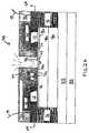
- FIGS. 1A and 1Billustrate a semiconductor device-based sensor 10 according to one embodiment of the invention.
- the sensoris a field effect transistor (FET) that includes a source electrode 12 , a drain electrode 14 and a gate electrode 16 formed on a semiconductor material (e.g., gallium nitride material) region 18 .
- the semiconductor material regionis formed on a substrate 20 and, as shown, a transition layer 22 may be formed between the substrate and the semiconductor material region.
- the sensorincludes a sensing region 23 between the source and the drain electrodes.
- the sensing regioncomprises a sensing layer 24 and an underlying surface region 25 of the semiconductor material region.
- the sensing layeris a sensing electrode which, along with the gate electrode is defined, at least in part, by an electrode-defining layer 26 .
- sensing region 23is exposed to a medium (e.g., a fluid) that includes chemical species to be detected.
- a mediume.g., a fluid
- the chemical species in the mediume.g., by following the direction of the schematic arrows in FIG. 1A
- the sensing layerwhich leads to an interaction between the species and the sensing layer. It is believed that this interaction results in a change in the surface potential of underlying surface region 25 .
- This change in surface potentialresults in a change in a property (e.g., drain current) of the device which may be measured and related to the concentration of the species in the medium.
- the chemical speciesmay also diffuse through the sensing layer and directly interact with the underlying semiconductor material region 18 .
- the inventionis not limited to a particular mechanism by which the measurable property (e.g., drain current) of the device is changed and/or by which the surface potential of the underlying surface region changes.
- the chemical speciesinteracts with a sensing region in some manner which results in the property change.
- sensor 10is an FET in the illustrative embodiment of FIGS. 1A and 1B , it should be understood that the invention encompasses other types of semiconductor device-based sensors as described further below.
- a layerWhen a layer is referred to as being “on” or “over” another layer or substrate, it can be directly on the layer or substrate, or an intervening layer may also be present. A layer that is “directly on” another layer or substrate means that no intervening layer is present. It should also be understood that when a layer is referred to as “on” or “over” another layer or substrate, it may cover the entire layer or substrate, or a portion of the layer or substrate.
- Sensing layer 24may be formed of any suitable material that is capable of interacting with a chemical species being detected in a manner that results in a change in a measurable property (e.g., drain current) of the sensor.
- the sensing layeris formed of a conductive material (e.g., when the sensing layer is a sensing electrode).
- Suitable conductive sensing layer materialsinclude, but are not limited to, metals, metal compounds and doped semiconductor materials.
- the sensing layercomprises a noble metal (or one of its alloys) or a transition metal (or one of its alloys).
- the sensing layermay comprise one or more of the following metals: platinum, palladium, iridium, ruthenium, nickel, copper, rhodium, molybdenum, iron, cobalt, titanium, vanadium, tantalum, tungsten, chromium, magnesium, gold, silver, aluminum, tin, osmium, magnesium, zinc, as well as alloys of these metals and compounds of these metals.
- the sensing layermay be formed of non-conductive materials such as dielectric materials or polymeric materials.
- the sensing layermay comprise more than one layer, each having a different composition. In some embodiments, one or more layer may be formed above the sensing layer, or between the sensing layer and the semiconductor material region.
- the sensing layer materialmay be selected for its sensitivity to a particular chemical species.
- the sensing layermay preferably comprise a material that interacts with the chemical species in a manner that causes a relatively large change in surface potential of the underlying surface region.
- Suitable chemical species/material combinationsare known in the art. For example, platinum or palladium electrodes are particularly well suited in hydrogen sensors; and, tin oxide is particularly well suited in CO 2 or CO detectors.
- the sensing layermay be a sensing electrode that is connected to a voltage source.
- the sensing layer 24is an electrode, it should be formed of a material that is sufficiently conductive. However, it should be understood that, in other embodiments, the sensing layer is not an electrode.
- the sensing layermay have any suitable dimensions that enable the device to function as desired. Because the sensing layer is separated from the gate electrode, the dimensions and design of the sensing layer (e.g., when functioning as a sensing electrode) are not subject to any gate electrode design requirements. This increases the ability to tailor the dimensions of the sensing layer (e.g., when functioning as a sensing electrode) to improve sensor performance. In certain conventional sensors in which the gate electrode also functions as a sensing electrode (i.e., sensors that measure changes in drain current that result from adsorption of the chemical species on the surface of the gate electrode) there may be less freedom over the dimensions of this electrode because it must satisfy gate electrode requirements. Thus, because of the added dimensional freedom, sensors of the invention may have sensing layers that can be tailored to have improved sensor performance (i.e., sensitivity, responsivity, and recovery) compared to such conventional sensors.
- improved sensor performancei.e., sensitivity, responsivity, and recovery
- sensing layer 24may be thinner than typically possible in conventional sensors in which the gate electrode also functions as a sensing electrode. Thin sensing electrodes permit relatively rapid diffusion of chemical species through the electrode to surface region 25 which can improve sensitivity and responsivity of the sensor. Also, thin sensing layers enable rapid out diffusion of chemical species which may lead to improved sensor recovery times.
- the sensing layermay have a thickness of less than about 500 nanometers such as between about 5 nanometers and about 200 nanometers, or between about 50 nanometers and about 200 nanometers. In other embodiments, the sensing layers may be thicker and have a thickness of greater than about 500 nanometers.
- the surface area of the sensing layeris designed to enable sufficient amounts of the chemical species to be adsorbed during operation. It may be advantageous in highly sensitive sensor applications for sensing layers to have a relatively large surface area when compared to the total channel surface area (i.e., the area defined between the source electrode and the drain electrode) of the device. In some cases, the ratio of the sensing electrode surface area to the total channel surface area is greater than about 0.35. In some cases, the ratio of the sensing electrode surface area to the total channel surface area is between about 0.20 and about 0.95; and, in some cases, between about 0.35 and about 0.60.
- sensing layer 24is separated from gate electrode 16 so that the sensor includes four different electrodes when the sensing layer is a sensing electrode.
- an external voltagemay be applied independently to each of the electrodes (i.e., source, gate, drain and sensing). Though, it should also be understood that the same external voltage may be applied to more than one of the different electrodes.
- the ability to independently control the voltages applied to different electrodesmay enhance the sensitivity and/or concentration range of the sensor for detecting a chemical species.
- the sensitivity and/or rangemay be enhanced as compared to conventional sensors that include a gate electrode that also functions as a sensing electrode because of the additional degree of freedom provided when the sensing electrode is separate from the gate electrode.
- the voltages applied to the different electrodesmay be selected such that the dependency of the drain current on the concentration of adsorbed species is increased or maximized.
- the gate electrodeis biased near the maximum transconductance of the FET device while the source is grounded and the drain is positively biased. In this mode, small changes in the surface potential of the surface region 25 may translate into relatively large changes in drain current which results in high sensitivity.
- sensing region 23is separated from the gate electrode which means that the sensing region is located at a different position on the device than the gate electrode and the region directly beneath the gate electrode. Thus, the sensing region is laterally separated from the gate electrode in the illustrative embodiment. As shown, the sensing region is positioned between the source and the drain electrodes and, more particularly, between the gate and drain electrodes. It should be understood that the sensing region may be positioned in other locations including between the source and gate electrodes.
- substrate 20is a silicon substrate.
- a silicon substraterefers to any substrate that includes a silicon surface.
- suitable silicon substratesinclude substrates that are composed entirely of silicon (e.g., bulk silicon wafers), silicon-on-insulator (SOI) substrates, silicon-on-sapphire substrate (SOS), and SIMOX substrates, amongst others.
- Suitable silicon substratesalso include substrates that have a silicon wafer bonded to another material such as diamond, AlN, or other polycrystalline materials. Silicon substrates having different crystallographic orientations may be used. In some cases, silicon (111) substrates are preferred. In other cases, silicon (100) substrates are preferred.
- substratesmay also be used including sapphire, silicon carbide, indium phosphide, silicon germanium, gallium arsenide, gallium nitride material, aluminum nitride, or other III-V compound substrates.
- silicon substratesmay also be used including sapphire, silicon carbide, indium phosphide, silicon germanium, gallium arsenide, gallium nitride material, aluminum nitride, or other III-V compound substrates.
- silicon substratesin embodiments that do not use silicon substrates, all of the advantages associated with silicon substrates may not be achieved.
- the illustrative embodimentsinclude a substrate
- the substratemay be removed during processing.
- the substratemay also function as the semiconductor material region. That is, the substrate and semiconductor material region are the same region.
- the substrate (and semiconductor material region)may be formed of a gallium nitride material.
- Substrate 20may have any suitable dimensions. Suitable wafer diameters include, but are not limited to, 2 inches (50 mm), 4 inches (100 mm), 6 inches (150 mm), and 8 inches (200 mm). The diameter of the wafer depends, in part, on the type of substrate and the composition of the semiconductor material region. In some cases, it may be preferable for the substrate to be relatively thick, such as greater than about 125 micron (e.g., between about 125 micron and about 800 micron, or between about 400 micron and 800 micron). Relatively thick substrates may be easy to obtain, process, and can resist bending which can occur, in some cases, in thinner substrates.
- thinner substratese.g., less than 125 microns
- the substrateinitially is relatively thick (e.g., between about 200 microns and 800 microns) and then is thinned during a later processing step (e.g., to less than 150 microns).
- the substrateis substantially planar in the final device or structure.
- Substantially planar substratesmay be distinguished from substrates that are textured and/or have trenches formed therein (e.g., as in U.S. Pat. No. 6,265,289).
- the regions/layers formed on the substratee.g., transition layer, gallium nitride material region, and the like
- regions/layersmay be grown in vertical (e.g., non-lateral) growth processes.
- Planar substrates and regions/layerscan be advantageous in some embodiments, for example, to simplify processing. Though it should be understood that, in some embodiments of the invention, lateral growth processes may be used as described further below.
- Transition layer 22may optionally be formed on substrate 20 prior to the deposition of semiconductor material (e.g., gallium nitride material) region 18 .
- semiconductor materiale.g., gallium nitride material
- the presence of the transition layerdepends, in part, on the type of substrate and the composition of the semiconductor material region. When the substrate is a silicon substrate and the semiconductor material region is a gallium nitride material region, the presence of the transition layer may be preferred.
- the transition layermay accomplish one or more of the following: reducing crack formation in the semiconductor material (e.g., gallium nitride material) region by lowering thermal stresses arising from differences between the thermal expansion rates of the semiconductor material region and the substrate; reducing defect formation in semiconductor material region by lowering lattice stresses arising from differences between the lattice constants of the semiconductor material region and the substrate; and, increasing conduction between the substrate and semiconductor material region by reducing differences between the band gaps of substrate and gallium nitride materials.
- the presence of the transition layermay be particularly preferred when utilizing silicon substrates and gallium nitride material regions because of the large differences in thermal expansion rates and lattice constants between gallium nitride materials and silicon. It should be understood that the transition layer also may be formed between substrate 20 and gallium nitride material region for a variety of other reasons. In some cases, for example when a silicon substrate is not used, the device may not include a transition layer.
- the composition of transition layer 22depends, at least in part, on the compositions of the substrate and of the semiconductor material region.
- the transition layermay preferably comprise a compositionally-graded transition layer having a composition that is varied across at least a portion of the layer.
- Suitable compositionally-graded transition layersfor example, have been described in commonly-owned U.S. Pat. No. 6,649,287, entitled “Gallium Nitride Materials and Methods,” filed on Dec. 14, 2000, which is incorporated herein by reference.
- Compositionally-graded transition layersare particularly effective in reducing crack formation in the gallium nitride material region by lowering thermal stresses that result from differences in thermal expansion rates between the gallium nitride material and the substrate (e.g., silicon).
- the transition layeris compositionally graded and formed of an alloy of gallium nitride such as Al x In y Ga (1-x-y) N, Al x Ga (1-x) N, and In y Ga (1-y) N.
- the concentration of at least one of the elements (e.g., Ga, Al, In) of the alloyis varied across at least a portion of the thickness of the transition layer.
- the transition layerhas an Al x In y Ga (1-x-y) N composition
- x and/or ymay be varied.
- the transition layerhas a Al x Ga (1-x) N composition
- xmay be varied.
- ymay be varied.
- the transition layermay have a low gallium concentration at a back surface which is graded to a high gallium concentration at a front surface. It has been found that such transition layers are particularly effective in relieving internal stresses within the gallium nitride material region.
- the transition layermay have a composition of Al x Ga (1-x) N, where x is decreased from the back surface to the front surface of the transition layer (e.g., x is decreased from a value of 1 at the back surface of the transition layer to a value of 0 at the front surface of the transition layer).
- the composition of the transition layerfor example, may be graded discontinuously (e.g., step-wise) or continuously.
- One discontinuous grademay include steps of AlN, Al 0.6 Ga 0.4 N and Al 0.3 Ga 0.7 N proceeding in a direction toward the semiconductor material (e.g., gallium nitride material) region.
- the transition layerhas a monocrystalline (i.e., single crystal) structure. In some embodiments, transition layer 22 has a constant (i.e., non-varying) composition across its thickness.
- sensors of the inventionmay also optionally include other layers that are not depicted in the figures.
- the sensormay include one or more intermediate layers (e.g., a strain-absorbing layer).
- One or more intermediate layersmay be formed, for example, between the substrate and the transition layer (e.g., a compositionally-graded transition layer) and/or between the transition layer and the semiconductor material region. These layers may have a constant composition.
- an intermediate layermay be formed of a nitride-based compound such as gallium nitride alloy (such as Al x In y Ga (1-x-y )N, Al x Ga (1-x) N, or In y Ga (1-y) N), aluminum nitride, or aluminum nitride alloys.
- gallium nitride alloysuch as Al x In y Ga (1-x-y )N, Al x Ga (1-x) N, or In y Ga (1-y) N
- aluminum nitridesuch as Al x In y Ga (1-x-y )N, Al x Ga (1-x) N, or In y Ga (1-y) N
- aluminum nitridesuch as aluminum nitride, or aluminum nitride alloys.
- Suitable strain-absorbing layerse.g., silicon nitride material-based layers
- silicon nitride material-based layershave been described in commonly-owned, co-pending U.S. patent application Ser. No. ______, not yet assigned, entitled “Gallium Nitride Materials and Methods Associated With the Same”, filed Jun. 28, 2004, which is incorporated herein by reference.
- the intermediate layer(s)have a monocrystalline structure. In other cases, the intermediate layer(s) may have an amorphous structure (e.g., when the intermediate layer is a strain-absorbing layer comprising a silicon nitride-based material).
- semiconductor material region 18it is preferable for semiconductor material region 18 to comprise a gallium nitride material, at least in the area of surface region 25 .
- Gallium nitride materialshave electrical properties (e.g., high piezoresistivity) that make them well suited for use in certain sensors of the present invention.
- the surface potential of a gallium nitride material regionmay be strongly dependent on the adsorption of chemical species by the sensing region. This strong dependency can enable the sensor to be highly sensitive.
- Gallium nitride materialsare also generally able to withstand extreme conditions (such as high temperatures and/or corrosive environments) which certain other semiconductor materials cannot withstand.
- sensors that include gallium nitride material semiconductor regionsmay be able to operate under certain extreme conditions (and, thus, in certain applications) that sensors that include semiconductor regions formed of materials other than gallium nitride material.
- gallium nitride materialrefers to gallium nitride (GaN) and any of its alloys, such as aluminum gallium nitride (Al x Ga (1-x) N), indium gallium nitride (In y Ga (1-y) N), aluminum indium gallium nitride (Al x In y Ga (1-x-y) N), gallium arsenide phosporide nitride (GaAs a P b N (1-a-b) ), aluminum indium gallium arsenide phosporide nitride (Al x In y Ga (1-x-y) As a P b N (1-a-b) ), amongst others.
- Gallium nitride materialsmay be doped n-type or p-type, or may be intrinsic. Suitable gallium nitride materials have been described in U.S. Pat. No. 6,649,287, incorporated by reference above.
- semiconductor material regionmay include multiple semiconductor layers (e.g., 18 a , 18 b , 18 c )
- Layer 18 bmay have a different composition than layer 18 a .
- layer 18 bmay be formed of a first gallium nitride material and layer 18 a may be formed of a second gallium nitride material.
- the value of x in the gallium nitride material of layer 18 bmay have a value that is between 0.05 and 1.0 greater than the value of x in the gallium nitride material of layer 18 a , or between 0.05 and 0.5 greater than the value of x in the gallium nitride material of layer 18 a .
- layer 18 bmay be formed of Al 0.26 Ga 0.74 N, while layer 18 a is formed of GaN.
- layer 18 cmay be formed of GaN.
- semiconductor material region 18may be formed of only a single semiconductor material. Or, region 18 may be formed of a semiconductor material layer and other non-semiconductor layers including oxide layers and/or metallic layers. However, in these embodiments, it may be preferable for surface region 25 to comprise gallium nitride material to achieve the advantages associated with gallium nitride material described above.
- semiconductor material region 18may be formed primarily, or entirely, of semiconductor materials other than gallium nitride material.
- the semiconductor material regionmay be formed of silicon, gallium arsenide, or other III-V compounds.
- at least some of the advantages associated with gallium nitride materialsmay not be achieved when using other semiconductor materials.
- Semiconductor material region 18is of high enough quality to permit operation of the sensor device.
- the semiconductor material (e.g., gallium nitride material) regionhas a low crack level and a low defect level.
- transition layer 22may reduce crack and/or defect formation.
- the semiconductor material regionhas a defect density of less than about 10 9 defects/cm 2 .
- Gallium nitride materials having low crack levelshave been described in U.S. Pat. No. 6,649,287 incorporated by reference above.
- the semiconductor regionmay comprise gallium nitride materials having a crack level of less than 0.005 micron/micron 2 or a crack level of less than 0.001 micron/micron 2 .
- the semiconductor material regionincludes a layer or layers which have a monocrystalline (i.e., single crystal) structure.
- the gallium nitride materialmay have a single crystal structure such as a Wurtzite (hexagonal) structure.
- the thickness of semiconductor material region 18 and the number of different layersare dictated, at least in part, by the requirements of the specific device. At a minimum, the thickness of the semiconductor material region is sufficient to permit formation of the desired structure or device (e.g., FET).
- the semiconductor regionmay have a thickness of greater than 0.1 micron, though not always. In other cases, the semiconductor material region has a thickness of greater than 0.5 micron, greater than 2.0 microns, or even greater than 5.0 microns.
- electrode-defining layer 26defines, at least in part, gate electrode 16 and sensing layer 24 (which is a sensing electrode).
- a first via 30 ais formed in the electrode-defining layer in which the gate electrode is, in part, formed. The shape and the dimensions of the first via and, thus the gate electrode, can be controlled to improve certain electrical properties of the device.
- a second via 30 bis formed in the electrode-defining layer in which the sensing layer is, in part, formed. The shape and the dimensions of the second via and, thus the sensing layer, can be controlled as desired.
- Suitable compositions for the electrode-defining layerinclude, but are not limited to, nitride-based compounds (e.g., silicon nitride compounds), oxide-based compounds (e.g., silicon oxide compounds), polyimides, other dielectric materials, or combinations of these compositions (e.g., silicon oxide and silicon nitride).
- nitride-based compoundse.g., silicon nitride compounds
- oxide-based compoundse.g., silicon oxide compounds
- polyimidese.g., other dielectric materials, or combinations of these compositions (e.g., silicon oxide and silicon nitride).
- the electrode-defining layerit may be preferable for the electrode-defining layer to be a silicon nitride compound (e.g., Si 3 N 4 ) or non-stoichiometric silicon nitride compounds.
- the electrode-defining layeris directly on semiconductor material region 18 and functions as a passivating layer that protects and passivates the surface of the semiconductor material region (e.g., gallium nitride material) region.
- the semiconductor material regione.g., gallium nitride material
- the sensors of the inventionmay not include a layer that defines the gate electrode and/or the sensing layer.
- the gate electrode and/or sensing layerare otherwise patterned to form the desired structure.
- the gate, source and drain electrodesmay be formed of any suitable conducting material such as metals (e.g., gold, nickel), metal compounds (e.g., WSi, WSiN), alloys, semiconductors, or combinations of these materials.
- the gate electrodemay be formed of gold, nickel or both.
- Source and drain electrodesmay be formed of gold, nickel, titanium, aluminum, platinum or silicon. Such compositions are known to those of ordinary skill in the art.
- the electrodesmay extend into the semiconductor material region.
- electrode materiale.g., metal
- deposited on the surface of the gallium nitride material regionmay diffuse into the semiconductor material region during a subsequent annealing step (e.g., RTA) when forming the electrode.
- the source and drain electrodesmay include such a portion diffused into the semiconductor material region. As used herein, such electrodes are still considered to be formed on the semiconductor material region.
- the sensor shown in FIGS. 1A and 1Bincludes an encapsulation layer 32 which, as known to those of skill in the art, encapsulates underlying layers of the structure to provide chemical and/or electrical protection.
- the encapsulation layermay be formed of any suitable material including oxides or nitrides.
- An opening 34is formed in the encapsulation layer to allow chemical species access to the sensing electrode.
- the openingmay has sloped sidewalls so that the cross-sectional area of the opening decreases in a direction toward the sensing electrode which may enhance access to the sensing electrode.
- interconnects 35are provided as conductive pathways that are connected to electrodes of the sensor. Though the illustrated interconnects are connected to the source and drain electrodes, it should also be understood that other conductive interconnects (not shown) may be connected to the other electrodes (e.g., gate and sensing). Bond wires 37 are generally provided to electrically connect the interconnects to a voltage source, thus, providing a conductive pathway from the voltage source to the electrodes on the device.
- amorphized regions 36electrically isolate devices from adjacent devices (not shown).
- the amorphized regionsmay be formed by implanting a species (e.g., nitrogen ions) as described in commonly-owned, co-pending U.S. patent application Ser. No. ______, entitled “Gallium Nitride Material Structures Including Isolation Regions and Methods”, filed Jun. 28, 2004. It should be understood that other techniques for isolating adjacent devices may be utilized. In some cases, it may not be necessary to isolate adjacent devices and, thus, amorphized regions (or other features that isolate adjacent devices) may not be present.
- a speciese.g., nitrogen ions
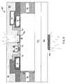
- FIGS. 2A and 2Billustrate a semiconductor device-based sensor 40 according to another embodiment of the invention.
- Sensor 40includes a sensing region 42 which is formed of an exposed surface of semiconductor material (e.g., gallium nitride material) region 18 .
- semiconductor materiale.g., gallium nitride material
- the chemical speciesare adsorbed directly on sensing region 42 .
- the surface potential of the semiconductor materiale.g., gallium nitride material
- This change in surface potentialleads to a change in a measurable property (e.g., drain current) of the device.
- a measurable propertye.g., drain current
- One advantage associated with the embodiments of FIGS. 2A and 2Bis that direct modification of the surface energy of the semiconductor material surface, particularly when the semiconductor material is a gallium nitride material, can lead to increased sensitivity, responsivity and recovery of the sensor.
- These improved propertiesarise because the surface potential of the semiconductor material (particularly, when the semiconductor material is a gallium nitride material) can be strongly dependent on the concentration of adsorbed chemical species and also the drain current can be strongly dependent on the surface potential of the semiconductor material region.
- adsorption of even a small concentration of chemical speciescan change the surface potential of the semiconductor region which causes measurable changes in drain current.
- these sensor propertiesmay be improved relative to certain sensors that do not involve direct adsorption of the chemical species by a semiconductor material region but may involve adsorption by another feature of the structure (e.g., an electrode).
- the composition of semiconductor material region 18is selected so that its surface potential is appropriately sensitive to the adsorbed chemical species. Suitable compositions have been described above in connection with FIGS. 1A and 1B including suitable compositions of layers 18 b and 18 a.
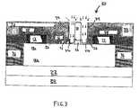
- FIG. 3illustrates a semiconductor device-based sensor 50 according to another embodiment of the invention.
- sensor 50includes a first sensing layer 24 a and a second sensing layer 24 b , both formed between the source electrode and the drain electrode.
- One, both, or neither of sensing layers 24 a , 24 bmay be sensing electrodes.
- the first and second sensing layersmay be used to detect the same or different chemical species. In some embodiments, the first and the second sensing layers need not be placed on the same side of the structure, as described further below.
- FIG. 4illustrates a semiconductor device-based sensor 60 according to another embodiment of the invention.
- Sensor 60includes a first sensing layer 24 c formed on a frontside of the sensor and second sensing layer 24 d formed on a backside of the sensor.
- the second sensing layermay be associated with a second device (not shown) (e.g., a second FET) formed in, or in regions below the substrate which is separate from the illustrated device formed over the substrate.
- Providing a sensor that includes two devicesmay facilitate detection of two species by having the first device detect a first species and the second device detect the second species.
- FIG. 5illustrates a semiconductor device-based sensor 62 according to another embodiment of the invention.
- Sensor 62includes a first sensing layer 24 e formed on a frontside of the sensor and second sensing layer 24 f formed in a via 64 that extends from a backside of the sensor.
- the second sensing layermay be associated with the FET device formed over the substrate. That is, the second sensing layer may interact with chemical species which leads to a change in the surface potential of semiconductor material region 18 , as described above.
- Via 64may also enhance heat removal from the sensor which may be important during operation of the device. Suitable backside vias have been described in commonly-owned U.S. Pat. No. 6,611,002, and in commonly-owned, co-pending U.S. patent application Ser. No. 09/792,409, entitled “Gallium Nitride Materials Including Thermally Conductive Regions”, filed Feb. 23, 2001, by Borges et. al., both of which are incorporated herein by reference.
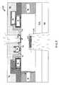
- FIG. 6illustrates a semiconductor device-based sensor 65 according to another embodiment of the invention.
- vias 66 a , 66 bextend from a backside of the sensor.
- Electrically conductive contacts 67 a , 67 bare deposited in respective vias 66 a , 66 b which are respectively connected to the source electrode 12 and drain electrode 14 .
- Contacts 67 a , 67 bextend onto the backside of the device.
- Bond wires 37are also provided for connecting the backside contacts to respective voltage sources.
- the frontside of the devicemay be free of contacts and bond wires. This enables all areas on the frontside of the device, except for the sensing region, to be encapsulated by encapsulation layer 32 .
- the encapsulation layermay provide chemical protection for the entire frontside of the device (except for the sensing region). This can be advantageous in applications in which the topside of the device is exposed to a corrosive environment that would otherwise damage electrical contacts, bond wires or others non-encapsulated regions (e.g., proximate electrical contacts) when located on the frontside of the device. Positioning electrical contacts at the backside may also facilitate device packaging.
- FIGS. 7A and 7Billustrate a semiconductor device-based sensor 70 according to another embodiment of the invention.
- sensor 70is a Schottky diode that include a Schottky electrode 72 and an ohmic electrode 74 that is formed around the diameter of the structure.
- the sensorfurther includes a sensing layer 24 g (which may be an electrode) between the Schottky electrode and the ohmic electrode which adsorbs chemical species as described above in connection with the other embodiments. As described above, the adsorption of the chemical species results in a change of a measurable property of the sensor (e.g., current).
- the sensing layer(s)may be replaced with a sensing region similar to those illustrated and described above in connection with FIGS. 2A and 2B .
- sensors of the inventionmay be based on other types of semiconductor devices than those illustrated in FIGS. 1-5 .
- other semiconductor devicesthat have measurable properties that may change in response to adsorption of a chemical species may be utilized.
- sensors of the inventionmay be based on devices that include a sensing electrode, separate from electrodes needed for conventional operation of the device.
- the sensing layermay be a sensing electrode separate from the source, drain and gate electrodes.
- the sensing layermay be a sensing electrode separate from the Schottky electrode and the ohmic electrode.
- chemical sensormay be integrated with other types of devices (e.g., a pressure sensor) in certain embodiments of the invention.
- Sensors of the present inventionmay be used in a wide variety of applications including engine emission monitoring, carbon dioxide detection and flue gas monitoring, amongst others. Also, the sensors of the present invention may be used to detect a wide variety of chemical species including, but not limited to, carbon dioxide, carbon monoxide, hydrogen, oxygen, nitrogen, nitrous oxide, hydrocarbons, alcohols and ionic species, amongst others. In some embodiments of the invention, it may be preferred for the sensors to detect the concentration of gaseous species.
- the chemical species being detectedinteract with a sensing region to create a change in the surface potential of an underlying semiconductor material region with this change in surface potential resulting in a change in a property (e.g., drain current) of the device.
- a propertye.g., drain current
- Sensors of the present inventionmay be formed using methods that employ conventional processing techniques.
- the layers of the structuremay be deposited, patterned and etched using conventional techniques.
- Transition layer 22 and semiconductor material (e.g., gallium nitride material) region 18may be deposited, for example, using metal organic chemical vapor deposition (MOCVD), molecular beam epitaxy (MBE), and hydride vapor phase epitaxy (HVPE), amongst other techniques.
- MOCVDmetal organic chemical vapor deposition
- MBEmolecular beam epitaxy
- HVPEhydride vapor phase epitaxy
- the preferred techniquemay depend, in part, on the composition of the layers.
- an MOCVD processmay be preferred.
- a suitable MOCVD process to form a transition layer (e.g., a compositionally-graded transition layer) and gallium nitride material region over a silicon substratehas been described in U.S. Pat. No. 6,649,287 incorporated by reference above.
- a single deposition stepe.g., an MOCVD step
- the processing parametersare suitably changed at the appropriate time to form the different layers.
- a single growth stepmay be used to form the transition layer and the semiconductor material (e.g., gallium nitride material) region.
- a semiconductor materiale.g., gallium nitride material
- LEOlateral epitaxial overgrowth
- the semiconductor material (e.g., gallium nitride material) regionusing a pendeoepitaxial technique that involves growing sidewalls of posts into trenches until growth from adjacent sidewalls coalesces to form a semiconductor material region, for example, as described in U.S. Pat. No. 6,265,289, which is incorporated herein by reference.
- semiconductor material (e.g., gallium nitride material) regions with very low defect densitiesare achievable.
- at least a portion of the semiconductor material (e.g., gallium nitride material) regionmay have a defect density of less than about 10 5 defects/cm 2 .
- Electrode-defining layer 26may be deposited using any suitable technique.
- CVDchemical vapor deposition
- PECVDplasma vapor deposition
- LP-CVDLP-CVD
- ECR-CVDLP-CVD
- ICP-CVDevaporation and sputtering.
- evaporation and sputteringevaporation and sputtering.
- Source, drain, gate and sensing electrodesmay be deposited on the semiconductor material region using known techniques such as an evaporation technique. In cases when the electrodes include two metals, then the metals are typically deposited in successive steps. The deposited metal layer may be patterned using conventional methods to form the electrodes.
- the sensing layermay be deposited using known techniques which may depend on the composition of the sensing layer.
- Electrode-defining layer 26 and electrodesSuitable techniques for forming electrode-defining layer 26 and electrodes have been described in commonly owned, co-pending U.S. patent application Ser. No. 10/740,376, filed on Dec. 17, 2003, and entitled “Gallium Nitride Material Devices Including an Electrode-Defining Layer and Methods of Forming the Same”, which is incorporated herein by reference above.
Landscapes
- Chemical & Material Sciences (AREA)
- Health & Medical Sciences (AREA)
- Microelectronics & Electronic Packaging (AREA)
- Life Sciences & Earth Sciences (AREA)
- Engineering & Computer Science (AREA)
- Chemical Kinetics & Catalysis (AREA)
- Physics & Mathematics (AREA)
- Electrochemistry (AREA)
- Analytical Chemistry (AREA)
- Biochemistry (AREA)
- General Health & Medical Sciences (AREA)
- General Physics & Mathematics (AREA)
- Immunology (AREA)
- Pathology (AREA)
- Power Engineering (AREA)
- Computer Hardware Design (AREA)
- Molecular Biology (AREA)
- Junction Field-Effect Transistors (AREA)
Abstract
Description
- The invention relates generally to semiconductor device-based sensors and, more particularly, to gallium nitride material-based transistors that function as chemical sensors and methods associated with the same.
- Sensors may be used in many applications, for example, to detect the concentration of a chemical species. The chemical species may be a component of a fluid (e.g., a gas or a liquid) to which the sensor is exposed.
- Semiconductor devices have been used as chemical sensors. For example, field effect transistor-based sensors may detect the concentration of a chemical species by measuring changes in drain current (i.e., source-to-drain current) that result from adsorption of the chemical species on the surface of the gate electrode. This adsorption may lead to a change in drain current. The change in the drain current may be related to the concentration of the adsorbed chemical species which, in turn, may be related to the concentration of the chemical species in the medium (e.g., fluid) being characterized.
- The invention provides semiconductor device-based sensors, as well as methods associated with the same.
- In one embodiment, a FET-based chemical sensor designed to detect a chemical species is provided. The sensor comprises a semiconductor material region. The sensor further comprises a source electrode, a drain electrode and a gate electrode, each formed on the semiconductor material region. The sensor further comprises a sensing region, separated from the gate electrode, and capable of interacting with the chemical species to change a measurable property of the chemical sensor.
- In another embodiment, a FET-based chemical sensor designed to detect a chemical species is provided. The sensor comprises a silicon substrate; a transition layer formed on the silicon substrate; and, a gallium nitride material region formed on the transition layer. The sensor further comprises a source electrode, a drain electrode and a gate electrode, each formed on the gallium nitride material region. The sensor further comprises a sensing region, separate from the gate electrode, and capable of interacting with the chemical species to change a drain current of the chemical sensor.
- In another embodiment, a semiconductor device-based chemical sensor is provided. The sensor comprises a semiconductor material region; and, a sensing electrode formed on the semiconductor material region. The sensing electrode is separated from electrodes needed for conventional operation of the device and is capable of interacting with the chemical species to change a measurable property of the chemical sensor.
- In another embodiment, a semiconductor device-based chemical sensor is provided. The sensor comprises a semiconductor material region. A first electrode and a second electrode are formed on the semiconductor material region. A first electrical contact extends from a backside of the sensor to the first electrode; and a second electrical contact extends from a backside of the sensor to the second electrode. The sensor further comprises a sensing region, separated from the first electrode and the second electrode, and capable of interacting with the chemical species to change a measurable property of the chemical sensor.
- In another embodiment, a method of detecting chemical species is provided. The method comprises exposing a FET-based chemical sensor to a medium comprising chemical species; and measuring changes in drain current of the sensor resulting from adsorption of the chemical species on a sensing region separated from the gate electrode to detect chemical species.
- Other aspects, embodiments and features of the invention will become apparent from the following detailed description of the invention when considered in conjunction with the accompanying drawings. The accompanying figures are schematic and are not intended to be drawn to scale. In the figures, identical, or substantially similar components that are illustrated in various figures may be represented by a single numeral or notation. For purposes of clarity, not every component is labeled in every figure. Nor is every component of each embodiment of the invention shown where illustration is not necessary to allow those of ordinary skill in the art to understand the invention. All patent applications and patents incorporated herein by reference are incorporated by reference in their entirety. In case of conflict with incorporated references, the present specification, including definitions, will control.
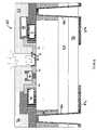
FIG. 1A is a cross-section of a field effect transistor (FET)-based chemical sensor including a sensing electrode according to an embodiment of the invention.FIG. 1B is a top view of the sensor ofFIG. 1A taken along line1B-1B inFIG. 1A .FIG. 2A is a cross-section of a FET-based chemical sensor including an exposed sensing region according to an embodiment of the invention.FIG. 2B is a top view of the sensor ofFIG. 2A taken along line2B-2B inFIG. 2A .FIG. 3 is a cross-section of a FET-based chemical sensor including two sensing electrodes according to an embodiment of the invention.FIG. 4 is a cross-section of a FET-based chemical sensor including two sensing electrodes respectively located on opposite sides of the sensor according to an embodiment of the invention.FIG. 5 is a cross-section of a FET-based chemical sensor including two sensing electrodes respectively located on opposite sides of the sensor according to an embodiment of the invention.FIG. 6 is a cross-section of a FET-based chemical sensor having backside electrical contacts according to an embodiment of the invention.FIGS. 7A and 7B respectively are a top view and a cross-section of a Schottky diode-based chemical sensor according to an embodiment of the invention.- The invention provides semiconductor device-based chemical sensors and methods associated with the same. The sensors include a sensing region that can interact with chemical species being detected. The chemical species may, for example, be a component of a fluid (e.g., gas or liquid). The interaction between the chemical species and a region of the sensor causes a change in a measurable property (e.g., an electrical property such as drain current) of the device. These changes may be related to the concentration of the chemical species in the medium being characterized. As described further below, the sensing region may be the combination of a sensing layer (e.g., a sensing electrode) and an underlying semiconductor material region, or an exposed semiconductor material (e.g., gallium nitride material) region. Sensors of the invention may be used in a wide variety of applications including engine emission monitoring, carbon dioxide detection and flue gas monitoring, amongst others.
FIGS. 1A and 1B illustrate a semiconductor device-basedsensor 10 according to one embodiment of the invention. In the illustrative embodiment, the sensor is a field effect transistor (FET) that includes asource electrode 12, adrain electrode 14 and agate electrode 16 formed on a semiconductor material (e.g., gallium nitride material)region 18. The semiconductor material region is formed on asubstrate 20 and, as shown, atransition layer 22 may be formed between the substrate and the semiconductor material region. The sensor includes asensing region 23 between the source and the drain electrodes. In the illustrative embodiment, the sensing region comprises asensing layer 24 and anunderlying surface region 25 of the semiconductor material region. As shown, the sensing layer is a sensing electrode which, along with the gate electrode is defined, at least in part, by an electrode-defininglayer 26.- During use,
sensing region 23 is exposed to a medium (e.g., a fluid) that includes chemical species to be detected. As described further below, the chemical species in the medium (e.g., by following the direction of the schematic arrows inFIG. 1A ) are adsorbed by the sensing layer which leads to an interaction between the species and the sensing layer. It is believed that this interaction results in a change in the surface potential ofunderlying surface region 25. This change in surface potential results in a change in a property (e.g., drain current) of the device which may be measured and related to the concentration of the species in the medium. - In some cases, it is believed that the chemical species may also diffuse through the sensing layer and directly interact with the underlying
semiconductor material region 18. However, it should be understood that the invention is not limited to a particular mechanism by which the measurable property (e.g., drain current) of the device is changed and/or by which the surface potential of the underlying surface region changes. In embodiments of the invention, the chemical species interacts with a sensing region in some manner which results in the property change. - Though
sensor 10 is an FET in the illustrative embodiment ofFIGS. 1A and 1B , it should be understood that the invention encompasses other types of semiconductor device-based sensors as described further below. - When a layer is referred to as being “on” or “over” another layer or substrate, it can be directly on the layer or substrate, or an intervening layer may also be present. A layer that is “directly on” another layer or substrate means that no intervening layer is present. It should also be understood that when a layer is referred to as “on” or “over” another layer or substrate, it may cover the entire layer or substrate, or a portion of the layer or substrate.
Sensing layer 24 may be formed of any suitable material that is capable of interacting with a chemical species being detected in a manner that results in a change in a measurable property (e.g., drain current) of the sensor. In some cases, the sensing layer is formed of a conductive material (e.g., when the sensing layer is a sensing electrode). Suitable conductive sensing layer materials include, but are not limited to, metals, metal compounds and doped semiconductor materials. In some embodiments, the sensing layer comprises a noble metal (or one of its alloys) or a transition metal (or one of its alloys). For example, the sensing layer may comprise one or more of the following metals: platinum, palladium, iridium, ruthenium, nickel, copper, rhodium, molybdenum, iron, cobalt, titanium, vanadium, tantalum, tungsten, chromium, magnesium, gold, silver, aluminum, tin, osmium, magnesium, zinc, as well as alloys of these metals and compounds of these metals.- It should also be understood that the above-described conductive materials may be suitable when the sensing layer is not functioning as an electrode.
- In other cases (e.g., when the sensing layer is not functioning as an electrode), the sensing layer may be formed of non-conductive materials such as dielectric materials or polymeric materials.
- In some embodiments, the sensing layer may comprise more than one layer, each having a different composition. In some embodiments, one or more layer may be formed above the sensing layer, or between the sensing layer and the semiconductor material region.
- The sensing layer material may be selected for its sensitivity to a particular chemical species. In cases when a highly sensitive sensor for a specific chemical species is desired, the sensing layer may preferably comprise a material that interacts with the chemical species in a manner that causes a relatively large change in surface potential of the underlying surface region. Suitable chemical species/material combinations are known in the art. For example, platinum or palladium electrodes are particularly well suited in hydrogen sensors; and, tin oxide is particularly well suited in CO2or CO detectors.
- As shown in
FIGS. 1A and 1B , the sensing layer may be a sensing electrode that is connected to a voltage source. When thesensing layer 24 is an electrode, it should be formed of a material that is sufficiently conductive. However, it should be understood that, in other embodiments, the sensing layer is not an electrode. - The sensing layer may have any suitable dimensions that enable the device to function as desired. Because the sensing layer is separated from the gate electrode, the dimensions and design of the sensing layer (e.g., when functioning as a sensing electrode) are not subject to any gate electrode design requirements. This increases the ability to tailor the dimensions of the sensing layer (e.g., when functioning as a sensing electrode) to improve sensor performance. In certain conventional sensors in which the gate electrode also functions as a sensing electrode (i.e., sensors that measure changes in drain current that result from adsorption of the chemical species on the surface of the gate electrode) there may be less freedom over the dimensions of this electrode because it must satisfy gate electrode requirements. Thus, because of the added dimensional freedom, sensors of the invention may have sensing layers that can be tailored to have improved sensor performance (i.e., sensitivity, responsivity, and recovery) compared to such conventional sensors.
- For example, sensing
layer 24 may be thinner than typically possible in conventional sensors in which the gate electrode also functions as a sensing electrode. Thin sensing electrodes permit relatively rapid diffusion of chemical species through the electrode to surfaceregion 25 which can improve sensitivity and responsivity of the sensor. Also, thin sensing layers enable rapid out diffusion of chemical species which may lead to improved sensor recovery times. For example, the sensing layer may have a thickness of less than about 500 nanometers such as between about 5 nanometers and about 200 nanometers, or between about 50 nanometers and about 200 nanometers. In other embodiments, the sensing layers may be thicker and have a thickness of greater than about 500 nanometers. - The surface area of the sensing layer is designed to enable sufficient amounts of the chemical species to be adsorbed during operation. It may be advantageous in highly sensitive sensor applications for sensing layers to have a relatively large surface area when compared to the total channel surface area (i.e., the area defined between the source electrode and the drain electrode) of the device. In some cases, the ratio of the sensing electrode surface area to the total channel surface area is greater than about 0.35. In some cases, the ratio of the sensing electrode surface area to the total channel surface area is between about 0.20 and about 0.95; and, in some cases, between about 0.35 and about 0.60.
- As noted above, in the embodiments of
FIGS. 1A and 1B ,sensing layer 24 is separated fromgate electrode 16 so that the sensor includes four different electrodes when the sensing layer is a sensing electrode. Thus, an external voltage may be applied independently to each of the electrodes (i.e., source, gate, drain and sensing). Though, it should also be understood that the same external voltage may be applied to more than one of the different electrodes. - The ability to independently control the voltages applied to different electrodes (and, in particular, independently controlling the voltage applied to the sensing electrode and the gate electrode) may enhance the sensitivity and/or concentration range of the sensor for detecting a chemical species. In particular, the sensitivity and/or range may be enhanced as compared to conventional sensors that include a gate electrode that also functions as a sensing electrode because of the additional degree of freedom provided when the sensing electrode is separate from the gate electrode. In the embodiment of
FIGS. 1A and 1B , the voltages applied to the different electrodes may be selected such that the dependency of the drain current on the concentration of adsorbed species is increased or maximized. In one preferred mode of operation, the gate electrode is biased near the maximum transconductance of the FET device while the source is grounded and the drain is positively biased. In this mode, small changes in the surface potential of thesurface region 25 may translate into relatively large changes in drain current which results in high sensitivity. - In the illustrative embodiment,
sensing region 23 is separated from the gate electrode which means that the sensing region is located at a different position on the device than the gate electrode and the region directly beneath the gate electrode. Thus, the sensing region is laterally separated from the gate electrode in the illustrative embodiment. As shown, the sensing region is positioned between the source and the drain electrodes and, more particularly, between the gate and drain electrodes. It should be understood that the sensing region may be positioned in other locations including between the source and gate electrodes. - In certain preferred embodiments,
substrate 20 is a silicon substrate. As used herein, a silicon substrate refers to any substrate that includes a silicon surface. Examples of suitable silicon substrates include substrates that are composed entirely of silicon (e.g., bulk silicon wafers), silicon-on-insulator (SOI) substrates, silicon-on-sapphire substrate (SOS), and SIMOX substrates, amongst others. Suitable silicon substrates also include substrates that have a silicon wafer bonded to another material such as diamond, AlN, or other polycrystalline materials. Silicon substrates having different crystallographic orientations may be used. In some cases, silicon (111) substrates are preferred. In other cases, silicon (100) substrates are preferred. - It should be understood that other types of substrates may also be used including sapphire, silicon carbide, indium phosphide, silicon germanium, gallium arsenide, gallium nitride material, aluminum nitride, or other III-V compound substrates. However, in embodiments that do not use silicon substrates, all of the advantages associated with silicon substrates may not be achieved.
- It should also be understood that though the illustrative embodiments include a substrate, other embodiments of the invention may not have a substrate. In these embodiments, the substrate may be removed during processing. In other embodiments, the substrate may also function as the semiconductor material region. That is, the substrate and semiconductor material region are the same region. For example, in these embodiments, the substrate (and semiconductor material region) may be formed of a gallium nitride material.
Substrate 20 may have any suitable dimensions. Suitable wafer diameters include, but are not limited to, 2 inches (50 mm), 4 inches (100 mm), 6 inches (150 mm), and 8 inches (200 mm). The diameter of the wafer depends, in part, on the type of substrate and the composition of the semiconductor material region. In some cases, it may be preferable for the substrate to be relatively thick, such as greater than about 125 micron (e.g., between about 125 micron and about 800 micron, or between about 400 micron and 800 micron). Relatively thick substrates may be easy to obtain, process, and can resist bending which can occur, in some cases, in thinner substrates. In other embodiments, thinner substrates (e.g., less than 125 microns) are used, though these embodiments may not have the advantages associated with thicker substrates, but can have other advantages including facilitating processing and/or reducing the number of processing steps. In some processes, the substrate initially is relatively thick (e.g., between about 200 microns and 800 microns) and then is thinned during a later processing step (e.g., to less than 150 microns).- In some preferred embodiments, the substrate is substantially planar in the final device or structure. Substantially planar substrates may be distinguished from substrates that are textured and/or have trenches formed therein (e.g., as in U.S. Pat. No. 6,265,289). In the illustrative embodiments, the regions/layers formed on the substrate (e.g., transition layer, gallium nitride material region, and the like) are also substantially planar. As described further below, such regions/layers may be grown in vertical (e.g., non-lateral) growth processes. Planar substrates and regions/layers can be advantageous in some embodiments, for example, to simplify processing. Though it should be understood that, in some embodiments of the invention, lateral growth processes may be used as described further below.
Transition layer 22 may optionally be formed onsubstrate 20 prior to the deposition of semiconductor material (e.g., gallium nitride material)region 18. The presence of the transition layer depends, in part, on the type of substrate and the composition of the semiconductor material region. When the substrate is a silicon substrate and the semiconductor material region is a gallium nitride material region, the presence of the transition layer may be preferred.- The transition layer may accomplish one or more of the following: reducing crack formation in the semiconductor material (e.g., gallium nitride material) region by lowering thermal stresses arising from differences between the thermal expansion rates of the semiconductor material region and the substrate; reducing defect formation in semiconductor material region by lowering lattice stresses arising from differences between the lattice constants of the semiconductor material region and the substrate; and, increasing conduction between the substrate and semiconductor material region by reducing differences between the band gaps of substrate and gallium nitride materials. The presence of the transition layer may be particularly preferred when utilizing silicon substrates and gallium nitride material regions because of the large differences in thermal expansion rates and lattice constants between gallium nitride materials and silicon. It should be understood that the transition layer also may be formed between
substrate 20 and gallium nitride material region for a variety of other reasons. In some cases, for example when a silicon substrate is not used, the device may not include a transition layer. - The composition of
transition layer 22 depends, at least in part, on the compositions of the substrate and of the semiconductor material region. In some embodiments which include a silicon substrate and a gallium nitride material region, the transition layer may preferably comprise a compositionally-graded transition layer having a composition that is varied across at least a portion of the layer. Suitable compositionally-graded transition layers, for example, have been described in commonly-owned U.S. Pat. No. 6,649,287, entitled “Gallium Nitride Materials and Methods,” filed on Dec. 14, 2000, which is incorporated herein by reference. Compositionally-graded transition layers are particularly effective in reducing crack formation in the gallium nitride material region by lowering thermal stresses that result from differences in thermal expansion rates between the gallium nitride material and the substrate (e.g., silicon). - According to one set of embodiments, the transition layer is compositionally graded and formed of an alloy of gallium nitride such as AlxInyGa(1-x-y)N, AlxGa(1-x)N, and InyGa(1-y)N. In these embodiments, the concentration of at least one of the elements (e.g., Ga, Al, In) of the alloy is varied across at least a portion of the thickness of the transition layer. When the transition layer has an AlxInyGa(1-x-y)N composition, x and/or y may be varied. When the transition layer has a AlxGa(1-x)N composition, x may be varied. When the transition layer has a InyGa(1-y)N composition, y may be varied.
- In certain preferred embodiments, it is desirable for the transition layer to have a low gallium concentration at a back surface which is graded to a high gallium concentration at a front surface. It has been found that such transition layers are particularly effective in relieving internal stresses within the gallium nitride material region. For example, the transition layer may have a composition of AlxGa(1-x)N, where x is decreased from the back surface to the front surface of the transition layer (e.g., x is decreased from a value of 1 at the back surface of the transition layer to a value of 0 at the front surface of the transition layer). The composition of the transition layer, for example, may be graded discontinuously (e.g., step-wise) or continuously. One discontinuous grade may include steps of AlN, Al0.6Ga0.4N and Al0.3Ga0.7N proceeding in a direction toward the semiconductor material (e.g., gallium nitride material) region.
- In some cases, the transition layer has a monocrystalline (i.e., single crystal) structure. In some embodiments,
transition layer 22 has a constant (i.e., non-varying) composition across its thickness. - In some embodiments, sensors of the invention may also optionally include other layers that are not depicted in the figures. For example, the sensor may include one or more intermediate layers (e.g., a strain-absorbing layer). One or more intermediate layers may be formed, for example, between the substrate and the transition layer (e.g., a compositionally-graded transition layer) and/or between the transition layer and the semiconductor material region. These layers may have a constant composition.
- Suitable intermediate layers, for example, have been described in U.S. Pat. No. 6,649,287, which is incorporated by reference above. In some embodiments, an intermediate layer may be formed of a nitride-based compound such as gallium nitride alloy (such as AlxInyGa(1-x-y)N, AlxGa(1-x)N, or InyGa(1-y)N), aluminum nitride, or aluminum nitride alloys.
- Suitable strain-absorbing layers (e.g., silicon nitride material-based layers), for example, have been described in commonly-owned, co-pending U.S. patent application Ser. No. ______, not yet assigned, entitled “Gallium Nitride Materials and Methods Associated With the Same”, filed Jun. 28, 2004, which is incorporated herein by reference.
- In some cases, the intermediate layer(s) have a monocrystalline structure. In other cases, the intermediate layer(s) may have an amorphous structure (e.g., when the intermediate layer is a strain-absorbing layer comprising a silicon nitride-based material).
- As noted above, in some embodiments of the invention, it is preferable for
semiconductor material region 18 to comprise a gallium nitride material, at least in the area ofsurface region 25. Gallium nitride materials have electrical properties (e.g., high piezoresistivity) that make them well suited for use in certain sensors of the present invention. For example, the surface potential of a gallium nitride material region may be strongly dependent on the adsorption of chemical species by the sensing region. This strong dependency can enable the sensor to be highly sensitive. - Gallium nitride materials are also generally able to withstand extreme conditions (such as high temperatures and/or corrosive environments) which certain other semiconductor materials cannot withstand. Thus, sensors that include gallium nitride material semiconductor regions may be able to operate under certain extreme conditions (and, thus, in certain applications) that sensors that include semiconductor regions formed of materials other than gallium nitride material.
- As used herein, the phrase “gallium nitride material” refers to gallium nitride (GaN) and any of its alloys, such as aluminum gallium nitride (AlxGa(1-x)N), indium gallium nitride (InyGa(1-y)N), aluminum indium gallium nitride (AlxInyGa(1-x-y)N), gallium arsenide phosporide nitride (GaAsaPbN(1-a-b)), aluminum indium gallium arsenide phosporide nitride (AlxInyGa(1-x-y)AsaPbN(1-a-b)), amongst others. Typically, when present, arsenic and/or phosphorous are at low concentrations (i.e., less than 5 weight percent). In certain preferred embodiments, the gallium nitride material has a high concentrations of gallium and nitrogen. In high gallium concentration embodiments, the sum of (x+y) may be less than 0.4, less than 0.2, less than 0.1, or even less. In some cases, it is preferable for the gallium nitride material layer to have a composition of GaN (i.e., x+y=0) or AlxGa(1-x)N (y=0). In some cases, when the gallium nitride material layer has a composition of AlxGa(1-x)N, x is less than about 0.4. Gallium nitride materials may be doped n-type or p-type, or may be intrinsic. Suitable gallium nitride materials have been described in U.S. Pat. No. 6,649,287, incorporated by reference above.
- As shown in certain embodiments, semiconductor material region may include multiple semiconductor layers (e.g.,18a,18b,18c) Layer18bmay have a different composition than layer18a. For example, layer18bmay be formed of a first gallium nitride material and layer18amay be formed of a second gallium nitride material. In certain embodiments, it may be preferable for the gallium nitride material of layer18bto have an aluminum concentration that is greater than the aluminum concentration of the gallium nitride material of layer18a. For example, the value of x in the gallium nitride material of layer18b(with reference to any of the gallium nitride materials described above) may have a value that is between 0.05 and 1.0 greater than the value of x in the gallium nitride material of layer18a, or between 0.05 and 0.5 greater than the value of x in the gallium nitride material of layer18a. For example, layer18bmay be formed of Al0.26Ga0.74N, while layer18ais formed of GaN. This difference in aluminum concentration may lead to formation of a highly conductive region at the interface of the layers18b,18a(i.e., a2-D electron gas region) which can increase the sensitivity of the surface potential of
surface region 25 which, in turn, can increase the sensitivity of the sensor. In the illustrative embodiment, layer18cmay be formed of GaN. - In some embodiments,
semiconductor material region 18 may be formed of only a single semiconductor material. Or,region 18 may be formed of a semiconductor material layer and other non-semiconductor layers including oxide layers and/or metallic layers. However, in these embodiments, it may be preferable forsurface region 25 to comprise gallium nitride material to achieve the advantages associated with gallium nitride material described above. - It should also be understood that, in certain embodiments of the invention,
semiconductor material region 18 may be formed primarily, or entirely, of semiconductor materials other than gallium nitride material. For example, the semiconductor material region may be formed of silicon, gallium arsenide, or other III-V compounds. However, at least some of the advantages associated with gallium nitride materials may not be achieved when using other semiconductor materials. Semiconductor material region 18 is of high enough quality to permit operation of the sensor device. Preferably, the semiconductor material (e.g., gallium nitride material) region has a low crack level and a low defect level. As described above, transition layer22 (particularly when compositionally-graded) may reduce crack and/or defect formation. In some embodiments, the semiconductor material region has a defect density of less than about 109defects/cm2.- Gallium nitride materials having low crack levels have been described in U.S. Pat. No. 6,649,287 incorporated by reference above. In some cases, the semiconductor region may comprise gallium nitride materials having a crack level of less than 0.005 micron/micron2or a crack level of less than 0.001 micron/micron2. In certain cases, it may be preferable for the semiconductor region to comprise gallium nitride material that is substantially crack-free as defined by a crack level of less than 0.0001 micron/micron2.
- In certain cases, the semiconductor material region includes a layer or layers which have a monocrystalline (i.e., single crystal) structure. In cases when the semiconductor region comprises gallium nitride material, the gallium nitride material may have a single crystal structure such as a Wurtzite (hexagonal) structure.
- The thickness of
semiconductor material region 18 and the number of different layers are dictated, at least in part, by the requirements of the specific device. At a minimum, the thickness of the semiconductor material region is sufficient to permit formation of the desired structure or device (e.g., FET). The semiconductor region may have a thickness of greater than 0.1 micron, though not always. In other cases, the semiconductor material region has a thickness of greater than 0.5 micron, greater than 2.0 microns, or even greater than 5.0 microns. - As noted above, in the illustrative embodiment, electrode-defining
layer 26 defines, at least in part,gate electrode 16 and sensing layer24 (which is a sensing electrode). A first via30ais formed in the electrode-defining layer in which the gate electrode is, in part, formed. The shape and the dimensions of the first via and, thus the gate electrode, can be controlled to improve certain electrical properties of the device. A second via30bis formed in the electrode-defining layer in which the sensing layer is, in part, formed. The shape and the dimensions of the second via and, thus the sensing layer, can be controlled as desired. - Suitable compositions for the electrode-defining layer include, but are not limited to, nitride-based compounds (e.g., silicon nitride compounds), oxide-based compounds (e.g., silicon oxide compounds), polyimides, other dielectric materials, or combinations of these compositions (e.g., silicon oxide and silicon nitride). In some cases, it may be preferable for the electrode-defining layer to be a silicon nitride compound (e.g., Si3N4) or non-stoichiometric silicon nitride compounds.
- In the illustrative embodiment, the electrode-defining layer is directly on
semiconductor material region 18 and functions as a passivating layer that protects and passivates the surface of the semiconductor material region (e.g., gallium nitride material) region. - Suitable electrode-defining layers and gate electrode structures have been described in commonly owned, co-pending U.S. patent application Ser. No. 10/740,376, filed on Dec. 17, 2003, and entitled “Gallium Nitride Material Devices Including an Electrode-Defining Layer and Methods of Forming the Same”, which is incorporated herein by reference.
- It should be understood that, in certain embodiments, the sensors of the invention may not include a layer that defines the gate electrode and/or the sensing layer. In these cases, the gate electrode and/or sensing layer are otherwise patterned to form the desired structure.
- The gate, source and drain electrodes may be formed of any suitable conducting material such as metals (e.g., gold, nickel), metal compounds (e.g., WSi, WSiN), alloys, semiconductors, or combinations of these materials. For example, the gate electrode may be formed of gold, nickel or both. Source and drain electrodes may be formed of gold, nickel, titanium, aluminum, platinum or silicon. Such compositions are known to those of ordinary skill in the art.
- In some embodiments, the electrodes may extend into the semiconductor material region. For example, electrode material (e.g., metal) deposited on the surface of the gallium nitride material region may diffuse into the semiconductor material region during a subsequent annealing step (e.g., RTA) when forming the electrode. In particular, the source and drain electrodes may include such a portion diffused into the semiconductor material region. As used herein, such electrodes are still considered to be formed on the semiconductor material region.
- The sensor shown in
FIGS. 1A and 1B includes anencapsulation layer 32 which, as known to those of skill in the art, encapsulates underlying layers of the structure to provide chemical and/or electrical protection. The encapsulation layer may be formed of any suitable material including oxides or nitrides. - An
opening 34 is formed in the encapsulation layer to allow chemical species access to the sensing electrode. In some embodiments, the opening may has sloped sidewalls so that the cross-sectional area of the opening decreases in a direction toward the sensing electrode which may enhance access to the sensing electrode. - In the illustrative embodiment, interconnects35 are provided as conductive pathways that are connected to electrodes of the sensor. Though the illustrated interconnects are connected to the source and drain electrodes, it should also be understood that other conductive interconnects (not shown) may be connected to the other electrodes (e.g., gate and sensing).
Bond wires 37 are generally provided to electrically connect the interconnects to a voltage source, thus, providing a conductive pathway from the voltage source to the electrodes on the device. - In the illustrative embodiment,
amorphized regions 36 electrically isolate devices from adjacent devices (not shown). The amorphized regions may be formed by implanting a species (e.g., nitrogen ions) as described in commonly-owned, co-pending U.S. patent application Ser. No. ______, entitled “Gallium Nitride Material Structures Including Isolation Regions and Methods”, filed Jun. 28, 2004. It should be understood that other techniques for isolating adjacent devices may be utilized. In some cases, it may not be necessary to isolate adjacent devices and, thus, amorphized regions (or other features that isolate adjacent devices) may not be present. FIGS. 2A and 2B illustrate a semiconductor device-basedsensor 40 according to another embodiment of the invention.Sensor 40 includes asensing region 42 which is formed of an exposed surface of semiconductor material (e.g., gallium nitride material)region 18. During operation, in this embodiment, the chemical species are adsorbed directly on sensingregion 42. It is believed that, in these embodiments, the surface potential of the semiconductor material (e.g., gallium nitride material) is changed by the adsorption of the chemical species. This change in surface potential leads to a change in a measurable property (e.g., drain current) of the device. As described above, by measuring changes in this property, it is possible to determine the concentration of the species adsorbed and, accordingly, the concentration of the species in the medium in which the sensor is placed.- One advantage associated with the embodiments of
FIGS. 2A and 2B is that direct modification of the surface energy of the semiconductor material surface, particularly when the semiconductor material is a gallium nitride material, can lead to increased sensitivity, responsivity and recovery of the sensor. These improved properties arise because the surface potential of the semiconductor material (particularly, when the semiconductor material is a gallium nitride material) can be strongly dependent on the concentration of adsorbed chemical species and also the drain current can be strongly dependent on the surface potential of the semiconductor material region. Thus, adsorption of even a small concentration of chemical species can change the surface potential of the semiconductor region which causes measurable changes in drain current. In some of these embodiments, these sensor properties may be improved relative to certain sensors that do not involve direct adsorption of the chemical species by a semiconductor material region but may involve adsorption by another feature of the structure (e.g., an electrode). - In the embodiments of
FIGS. 2A and 2B , the composition ofsemiconductor material region 18 is selected so that its surface potential is appropriately sensitive to the adsorbed chemical species. Suitable compositions have been described above in connection withFIGS. 1A and 1B including suitable compositions of layers18band18a. - Suitable surface areas for
region 42 and ratios of surface area to total device surface area have been described above in connection withFIGS. 1A and 1B . FIG. 3 illustrates a semiconductor device-basedsensor 50 according to another embodiment of the invention. In this illustrative embodiment,sensor 50 includes afirst sensing layer 24aand a second sensing layer24b, both formed between the source electrode and the drain electrode. One, both, or neither of sensing layers24a,24bmay be sensing electrodes. The first and second sensing layers may be used to detect the same or different chemical species. In some embodiments, the first and the second sensing layers need not be placed on the same side of the structure, as described further below.FIG. 4 illustrates a semiconductor device-based sensor60 according to another embodiment of the invention. Sensor60 includes a first sensing layer24cformed on a frontside of the sensor and second sensing layer24dformed on a backside of the sensor. In this illustrative embodiment, the second sensing layer may be associated with a second device (not shown) (e.g., a second FET) formed in, or in regions below the substrate which is separate from the illustrated device formed over the substrate. Providing a sensor that includes two devices may facilitate detection of two species by having the first device detect a first species and the second device detect the second species.FIG. 5 illustrates a semiconductor device-basedsensor 62 according to another embodiment of the invention.Sensor 62 includes a first sensing layer24eformed on a frontside of the sensor and second sensing layer24fformed in a via64 that extends from a backside of the sensor. In this illustrative embodiment, the second sensing layer may be associated with the FET device formed over the substrate. That is, the second sensing layer may interact with chemical species which leads to a change in the surface potential ofsemiconductor material region 18, as described above. Via64 may also enhance heat removal from the sensor which may be important during operation of the device. Suitable backside vias have been described in commonly-owned U.S. Pat. No. 6,611,002, and in commonly-owned, co-pending U.S. patent application Ser. No. 09/792,409, entitled “Gallium Nitride Materials Including Thermally Conductive Regions”, filed Feb. 23, 2001, by Borges et. al., both of which are incorporated herein by reference.FIG. 6 illustrates a semiconductor device-basedsensor 65 according to another embodiment of the invention. In this embodiment, vias66a,66b(and others not shown) extend from a backside of the sensor. Electricallyconductive contacts 67a,67b(and others not shown) are deposited in respective vias66a,66bwhich are respectively connected to thesource electrode 12 anddrain electrode 14.Contacts 67a,67bextend onto the backside of the device. It should be understood that other vias and electrically conductive contacts (both not shown) may be similarly formed for connection togate electrode 16 and sensing layer24 (when functioning as a sensing electrode).Bond wires 37 are also provided for connecting the backside contacts to respective voltage sources.- Suitable backside vias have been described in commonly-owned U.S. Pat. No. 6,611,002 and U.S. patent application Ser. No. 09/792,409, both of which are incorporated herein by reference above.
- By providing electrically connection to the backside of the device, it is possible to eliminate contacts and bond wires from the frontside of the device. Thus, in these embodiments, the frontside of the device may be free of contacts and bond wires. This enables all areas on the frontside of the device, except for the sensing region, to be encapsulated by
encapsulation layer 32. Thus, the encapsulation layer may provide chemical protection for the entire frontside of the device (except for the sensing region). This can be advantageous in applications in which the topside of the device is exposed to a corrosive environment that would otherwise damage electrical contacts, bond wires or others non-encapsulated regions (e.g., proximate electrical contacts) when located on the frontside of the device. Positioning electrical contacts at the backside may also facilitate device packaging. FIGS. 7A and 7B illustrate a semiconductor device-basedsensor 70 according to another embodiment of the invention. In this embodiment,sensor 70 is a Schottky diode that include aSchottky electrode 72 and anohmic electrode 74 that is formed around the diameter of the structure. The sensor further includes a sensing layer24g(which may be an electrode) between the Schottky electrode and the ohmic electrode which adsorbs chemical species as described above in connection with the other embodiments. As described above, the adsorption of the chemical species results in a change of a measurable property of the sensor (e.g., current).- It should also be understood that, in the embodiments of
FIGS. 3-7 , the sensing layer(s) may be replaced with a sensing region similar to those illustrated and described above in connection withFIGS. 2A and 2B . - It should be understood that sensors of the invention may be based on other types of semiconductor devices than those illustrated in
FIGS. 1-5 . For example, other semiconductor devices that have measurable properties that may change in response to adsorption of a chemical species may be utilized. - In general, sensors of the invention may be based on devices that include a sensing electrode, separate from electrodes needed for conventional operation of the device. As described above in connection with the FET embodiment of
FIGS. 1A and 1B , the sensing layer may be a sensing electrode separate from the source, drain and gate electrodes. As described above in connection with the Schottky diode embodiment ofFIGS. 7A and 7B , the sensing layer may be a sensing electrode separate from the Schottky electrode and the ohmic electrode. - It should also be understood that the chemical sensor may be integrated with other types of devices (e.g., a pressure sensor) in certain embodiments of the invention.
- Sensors of the present invention may be used in a wide variety of applications including engine emission monitoring, carbon dioxide detection and flue gas monitoring, amongst others. Also, the sensors of the present invention may be used to detect a wide variety of chemical species including, but not limited to, carbon dioxide, carbon monoxide, hydrogen, oxygen, nitrogen, nitrous oxide, hydrocarbons, alcohols and ionic species, amongst others. In some embodiments of the invention, it may be preferred for the sensors to detect the concentration of gaseous species.
- As noted above, during use, the chemical species being detected interact with a sensing region to create a change in the surface potential of an underlying semiconductor material region with this change in surface potential resulting in a change in a property (e.g., drain current) of the device. By measuring the change in the property over time, it is possible to determine the concentration of the species in the medium in which the sensor is placed.
- Sensors of the present invention may be formed using methods that employ conventional processing techniques. For example, the layers of the structure may be deposited, patterned and etched using conventional techniques.
Transition layer 22 and semiconductor material (e.g., gallium nitride material)region 18 may be deposited, for example, using metal organic chemical vapor deposition (MOCVD), molecular beam epitaxy (MBE), and hydride vapor phase epitaxy (HVPE), amongst other techniques. The preferred technique may depend, in part, on the composition of the layers. In some cases in which the semiconductor material region comprises gallium nitride material, an MOCVD process may be preferred. A suitable MOCVD process to form a transition layer (e.g., a compositionally-graded transition layer) and gallium nitride material region over a silicon substrate has been described in U.S. Pat. No. 6,649,287 incorporated by reference above. When the semiconductor material region has different layers, in some cases it is preferable to use a single deposition step (e.g., an MOCVD step) to form theentire region 18. When using the single deposition step, the processing parameters are suitably changed at the appropriate time to form the different layers. In certain preferred cases, a single growth step may be used to form the transition layer and the semiconductor material (e.g., gallium nitride material) region.- In other embodiments of the invention (not shown), it is possible to grow a semiconductor material (e.g., gallium nitride material) region using a lateral epitaxial overgrowth (LEO) technique that involves growing an underlying semiconductor material layer through mask openings and then laterally over the mask to form the region, for example, as described in U.S. Pat. No. 6,051,849, which is incorporated herein by reference.
- In other embodiments of the invention (not shown), it is possible to grow the semiconductor material (e.g., gallium nitride material) region using a pendeoepitaxial technique that involves growing sidewalls of posts into trenches until growth from adjacent sidewalls coalesces to form a semiconductor material region, for example, as described in U.S. Pat. No. 6,265,289, which is incorporated herein by reference. In these lateral growth techniques, semiconductor material (e.g., gallium nitride material) regions with very low defect densities are achievable. For example, at least a portion of the semiconductor material (e.g., gallium nitride material) region may have a defect density of less than about 105defects/cm2.
- Electrode-defining
layer 26 may be deposited using any suitable technique. The technique used, in part, depends on the composition of the electrode-defining layer. Suitable techniques include, but are not limited to CVD, PECVD, LP-CVD, ECR-CVD, ICP-CVD, evaporation and sputtering. When the electrode-defining layer is formed of a silicon nitride material, it may be preferable to use PECVD to deposit the layer. - Source, drain, gate and sensing electrodes may be deposited on the semiconductor material region using known techniques such as an evaporation technique. In cases when the electrodes include two metals, then the metals are typically deposited in successive steps. The deposited metal layer may be patterned using conventional methods to form the electrodes.
- When the sensing layer is not an electrode, the sensing layer may be deposited using known techniques which may depend on the composition of the sensing layer.
- Suitable techniques for forming electrode-defining
layer 26 and electrodes have been described in commonly owned, co-pending U.S. patent application Ser. No. 10/740,376, filed on Dec. 17, 2003, and entitled “Gallium Nitride Material Devices Including an Electrode-Defining Layer and Methods of Forming the Same”, which is incorporated herein by reference above. - It should be understood that the invention encompasses other methods than those specifically described herein. Also, variations to the method described above would be known to those of ordinary skill in the art and are within the scope of the invention.
- Having thus described several aspects of at least one embodiment of this invention, it is to be appreciated various alterations, modifications, and improvements will readily occur to those skilled in the art. Such alterations, modifications, and improvements are intended to be part of this disclosure, and are intended to be within the spirit and scope of the invention. Accordingly, the foregoing description and drawings are by way of example only.
Claims (39)
Priority Applications (3)
| Application Number | Priority Date | Filing Date | Title |
|---|---|---|---|
| US10/879,704US7361946B2 (en) | 2004-06-28 | 2004-06-28 | Semiconductor device-based sensors |
| PCT/US2005/022490WO2006012300A1 (en) | 2004-06-28 | 2005-06-24 | Semiconductor device-based sensors and methods associated with the same |
| US12/023,500US20080185616A1 (en) | 2004-06-28 | 2008-01-31 | Semiconductor device-based sensors and methods associated with the same |
Applications Claiming Priority (1)
| Application Number | Priority Date | Filing Date | Title |
|---|---|---|---|
| US10/879,704US7361946B2 (en) | 2004-06-28 | 2004-06-28 | Semiconductor device-based sensors |
Related Child Applications (1)
| Application Number | Title | Priority Date | Filing Date |
|---|---|---|---|
| US12/023,500ContinuationUS20080185616A1 (en) | 2004-06-28 | 2008-01-31 | Semiconductor device-based sensors and methods associated with the same |
Publications (2)
| Publication Number | Publication Date |
|---|---|
| US20050285155A1true US20050285155A1 (en) | 2005-12-29 |
| US7361946B2 US7361946B2 (en) | 2008-04-22 |
Family
ID=34982423
Family Applications (2)
| Application Number | Title | Priority Date | Filing Date |
|---|---|---|---|
| US10/879,704Expired - Fee RelatedUS7361946B2 (en) | 2004-06-28 | 2004-06-28 | Semiconductor device-based sensors |
| US12/023,500AbandonedUS20080185616A1 (en) | 2004-06-28 | 2008-01-31 | Semiconductor device-based sensors and methods associated with the same |
Family Applications After (1)
| Application Number | Title | Priority Date | Filing Date |
|---|---|---|---|
| US12/023,500AbandonedUS20080185616A1 (en) | 2004-06-28 | 2008-01-31 | Semiconductor device-based sensors and methods associated with the same |
Country Status (2)
| Country | Link |
|---|---|
| US (2) | US7361946B2 (en) |
| WO (1) | WO2006012300A1 (en) |
Cited By (37)
| Publication number | Priority date | Publication date | Assignee | Title |
|---|---|---|---|---|
| US20050285141A1 (en)* | 2004-06-28 | 2005-12-29 | Piner Edwin L | Gallium nitride materials and methods associated with the same |
| US20060054927A1 (en)* | 2004-09-10 | 2006-03-16 | National Central University | Sensor using a GaN transistor |
| US20060174692A1 (en)* | 2005-02-07 | 2006-08-10 | Ulrich Bonne | Wireless gas composition sensor system |
| US20060249750A1 (en)* | 2003-12-17 | 2006-11-09 | Nitronex Corporation | Gallium nitride material devices including an electrode-defining layer and methods of forming the same |
| US20070295985A1 (en)* | 2001-02-23 | 2007-12-27 | Nitronex Corporation | Gallium nitride material devices and methods of forming the same |
| US20080061323A1 (en)* | 2004-01-21 | 2008-03-13 | Hitachi, Ltd. | Examination apparatus for biological sample and chemical sample |
| CN101769941A (en)* | 2010-01-27 | 2010-07-07 | 中国科学院上海技术物理研究所 | Electronic detection method of device structure of GaN base photovoltaic detector |
| US20130126895A1 (en)* | 2005-12-02 | 2013-05-23 | International Rectifier Corporation | Gallium Nitride Devices with Vias |
| US20130126888A1 (en)* | 2011-11-21 | 2013-05-23 | Epowersoft, Inc. | Edge Termination by Ion Implantation in GaN |
| US20130334061A1 (en)* | 2012-06-07 | 2013-12-19 | Stichting Imec Nederland | Sensor for sensing the presence of at least one fluidum |
| US20140225202A1 (en)* | 2013-01-31 | 2014-08-14 | Sensirion Ag | Chemical sensor and method for manufacturing such a chemical sensor |
| US20140264471A1 (en)* | 2013-03-15 | 2014-09-18 | Life Technologies Corporation | Chemical device with thin conductive element |
| US9110015B2 (en) | 2010-09-24 | 2015-08-18 | Life Technologies Corporation | Method and system for delta double sampling |
| US9164070B2 (en) | 2010-06-30 | 2015-10-20 | Life Technologies Corporation | Column adc |
| US9239313B2 (en) | 2010-06-30 | 2016-01-19 | Life Technologies Corporation | Ion-sensing charge-accumulation circuits and methods |
| US9270264B2 (en) | 2012-05-29 | 2016-02-23 | Life Technologies Corporation | System for reducing noise in a chemical sensor array |
| US9618475B2 (en) | 2010-09-15 | 2017-04-11 | Life Technologies Corporation | Methods and apparatus for measuring analytes |
| EP2278308A4 (en)* | 2008-04-22 | 2017-04-19 | Ngk Spark Plug Co., Ltd. | Gas sensor |
| US9835585B2 (en) | 2013-03-15 | 2017-12-05 | Life Technologies Corporation | Chemical sensor with protruded sensor surface |
| US9841398B2 (en) | 2013-01-08 | 2017-12-12 | Life Technologies Corporation | Methods for manufacturing well structures for low-noise chemical sensors |
| US9852919B2 (en) | 2013-01-04 | 2017-12-26 | Life Technologies Corporation | Methods and systems for point of use removal of sacrificial material |
| US9927393B2 (en) | 2009-05-29 | 2018-03-27 | Life Technologies Corporation | Methods and apparatus for measuring analytes |
| US9951382B2 (en) | 2006-12-14 | 2018-04-24 | Life Technologies Corporation | Methods and apparatus for measuring analytes using large scale FET arrays |
| US9960253B2 (en) | 2010-07-03 | 2018-05-01 | Life Technologies Corporation | Chemically sensitive sensor with lightly doped drains |
| US9964515B2 (en) | 2008-10-22 | 2018-05-08 | Life Technologies Corporation | Integrated sensor arrays for biological and chemical analysis |
| US9970984B2 (en) | 2011-12-01 | 2018-05-15 | Life Technologies Corporation | Method and apparatus for identifying defects in a chemical sensor array |
| US9989489B2 (en) | 2006-12-14 | 2018-06-05 | Life Technnologies Corporation | Methods for calibrating an array of chemically-sensitive sensors |
| US9995708B2 (en) | 2013-03-13 | 2018-06-12 | Life Technologies Corporation | Chemical sensor with sidewall spacer sensor surface |
| CN108400232A (en)* | 2018-03-12 | 2018-08-14 | 浙江大学 | A kind of pressure sensor and its manufacturing method based on nickel germanium alloy/germanium schottky junction |
| US10100357B2 (en) | 2013-05-09 | 2018-10-16 | Life Technologies Corporation | Windowed sequencing |
| TWI647842B (en)* | 2013-08-22 | 2019-01-11 | 美商生命技術公司 | Chemical device with thin conductive element |
| US10365259B2 (en)* | 2016-03-18 | 2019-07-30 | Panasonic Intellectual Property Management Co., Ltd. | Hydrogen sensor including pair of electrodes and metal oxide layer and method of detecting hydrogen with hydrogen sensor |
| US10422767B2 (en) | 2013-03-15 | 2019-09-24 | Life Technologies Corporation | Chemical sensor with consistent sensor surface areas |
| US10451585B2 (en) | 2009-05-29 | 2019-10-22 | Life Technologies Corporation | Methods and apparatus for measuring analytes |
| US10458942B2 (en) | 2013-06-10 | 2019-10-29 | Life Technologies Corporation | Chemical sensor array having multiple sensors per well |
| CN112903755A (en)* | 2021-02-24 | 2021-06-04 | 太原理工大学 | Carbon dioxide sensor and preparation method thereof |
| US11307166B2 (en) | 2010-07-01 | 2022-04-19 | Life Technologies Corporation | Column ADC |
Families Citing this family (41)
| Publication number | Priority date | Publication date | Assignee | Title |
|---|---|---|---|---|
| US7312087B2 (en)* | 2000-01-11 | 2007-12-25 | Clinical Micro Sensors, Inc. | Devices and methods for biochip multiplexing |
| TWI375994B (en)* | 2004-09-01 | 2012-11-01 | Sumitomo Electric Industries | Epitaxial substrate and semiconductor element |
| US20090163384A1 (en) | 2007-12-22 | 2009-06-25 | Lucent Technologies, Inc. | Detection apparatus for biological materials and methods of making and using the same |
| JP2008034411A (en)* | 2006-07-26 | 2008-02-14 | Toshiba Corp | Nitride semiconductor device |
| US7868354B2 (en)* | 2006-11-08 | 2011-01-11 | Duke University | GaN-based nitric oxide sensors and methods of making and using the same |
| US11339430B2 (en) | 2007-07-10 | 2022-05-24 | Life Technologies Corporation | Methods and apparatus for measuring analytes using large scale FET arrays |
| US8349167B2 (en) | 2006-12-14 | 2013-01-08 | Life Technologies Corporation | Methods and apparatus for detecting molecular interactions using FET arrays |
| DE102007020039B4 (en)* | 2007-04-27 | 2011-07-14 | Infineon Technologies Austria Ag | Method for producing a vertically inhomogeneous platinum or gold distribution in a semiconductor substrate and in a semiconductor component, semiconductor substrate and semiconductor component produced in this way |
| JP5431667B2 (en)* | 2007-10-01 | 2014-03-05 | 富士電機株式会社 | Gallium nitride semiconductor device |
| US7999288B2 (en)* | 2007-11-26 | 2011-08-16 | International Rectifier Corporation | High voltage durability III-nitride semiconductor device |
| US8143654B1 (en)* | 2008-01-16 | 2012-03-27 | Triquint Semiconductor, Inc. | Monolithic microwave integrated circuit with diamond layer |
| WO2009137768A2 (en)* | 2008-05-09 | 2009-11-12 | University Of Florida Research Foundation, Inc. | Oxygen and carbon dioxide sensing |
| US9970897B2 (en)* | 2008-06-16 | 2018-05-15 | Duke University | Chemical sensors and methods for making and using the same |
| CN102203282B (en) | 2008-06-25 | 2014-04-30 | 生命技术公司 | Methods and apparatus for measuring analytes using large scale FET arrays |
| TWI375029B (en)* | 2008-07-16 | 2012-10-21 | Nat Univ Tsing Hua | Field effect transistor based sensor |
| US20100301398A1 (en) | 2009-05-29 | 2010-12-02 | Ion Torrent Systems Incorporated | Methods and apparatus for measuring analytes |
| US9958442B2 (en) | 2009-02-11 | 2018-05-01 | Duke University | Sensors incorporating antibodies and methods of making and using the same |
| US8008691B2 (en)* | 2009-07-21 | 2011-08-30 | National Tsing Hua University | Ion sensitive field effect transistor and production method thereof |
| DE102009045475B4 (en) | 2009-10-08 | 2023-06-29 | Robert Bosch Gmbh | Gas-sensitive semiconductor device and use thereof |
| TWI539172B (en) | 2010-06-30 | 2016-06-21 | 生命技術公司 | Methods and apparatus for testing isfet arrays |
| US9470650B2 (en) | 2010-10-21 | 2016-10-18 | Carnegie Mellon University | Two-dimensional electron gas (2DEG)-based chemical sensors |
| CN103329256B (en) | 2010-12-15 | 2016-09-21 | 宜普电源转换公司 | There is the semiconductor device of rear surface isolation |
| EP2707631B1 (en)* | 2011-05-12 | 2017-02-15 | Fraunhofer Gesellschaft zur Förderung der angewandten Forschung E.V. | Test station and method for testing fluidic components |
| US8541849B2 (en) | 2012-02-14 | 2013-09-24 | Genia Technologies, Inc. | Noise shielding techniques for ultra low current measurements in biochemical applications |
| US8962366B2 (en) | 2013-01-28 | 2015-02-24 | Life Technologies Corporation | Self-aligned well structures for low-noise chemical sensors |
| US8871549B2 (en)* | 2013-02-14 | 2014-10-28 | International Business Machines Corporation | Biological and chemical sensors |
| US8841217B1 (en) | 2013-03-13 | 2014-09-23 | Life Technologies Corporation | Chemical sensor with protruded sensor surface |
| US20140264468A1 (en)* | 2013-03-14 | 2014-09-18 | Taiwan Semiconductor Manufacturing Company, Ltd. | Biofet with increased sensing area |
| US9116117B2 (en) | 2013-03-15 | 2015-08-25 | Life Technologies Corporation | Chemical sensor with sidewall sensor surface |
| EP2972279B1 (en)* | 2013-03-15 | 2021-10-06 | Life Technologies Corporation | Chemical sensors with consistent sensor surface areas |
| US9170193B2 (en) | 2013-06-06 | 2015-10-27 | General Electric Company | Detecting coolant leaks in turbine generators |
| US9097657B2 (en) | 2013-07-23 | 2015-08-04 | General Electric Company | Leak detection of stator liquid cooling system |
| TWI655429B (en)* | 2013-11-06 | 2019-04-01 | 美商生命技術公司 | Chemical sensors with consistent sensor surface areas and method manufacturing the same |
| US10407716B2 (en) | 2014-03-13 | 2019-09-10 | Duke University | Electronic platform for sensing and control of electrochemical reactions |
| US10043990B2 (en)* | 2014-07-23 | 2018-08-07 | University Of Utah Research Foundation | Dual-gate chemical field effect transistor sensor |
| CN107407656B (en) | 2014-12-18 | 2020-04-07 | 生命科技公司 | Method and apparatus for measuring analytes using large scale FET arrays |
| US10077472B2 (en) | 2014-12-18 | 2018-09-18 | Life Technologies Corporation | High data rate integrated circuit with power management |
| KR102593647B1 (en) | 2014-12-18 | 2023-10-26 | 라이프 테크놀로지스 코포레이션 | High data rate integrated circuit with transmitter configuration |
| JP6432672B2 (en)* | 2015-03-10 | 2018-12-05 | 富士通株式会社 | Gas sensor and sensor device |
| US10083856B2 (en)* | 2016-08-01 | 2018-09-25 | Taiwan Semiconductor Manufacturing Company Limited | Isolation regions for semiconductor structures and methods of forming the same |
| CN112345614B (en)* | 2019-08-08 | 2023-07-21 | 中国科学院微电子研究所 | Detector based on gallium nitride-based enhancement device and manufacturing method thereof |
Citations (88)
| Publication number | Priority date | Publication date | Assignee | Title |
|---|---|---|---|---|
| US4020830A (en)* | 1975-03-12 | 1977-05-03 | The University Of Utah | Selective chemical sensitive FET transducers |
| US4180771A (en)* | 1977-12-02 | 1979-12-25 | Airco, Inc. | Chemical-sensitive field-effect transistor |
| US4411741A (en)* | 1982-01-12 | 1983-10-25 | University Of Utah | Apparatus and method for measuring the concentration of components in fluids |
| US4636827A (en)* | 1981-07-24 | 1987-01-13 | Fondation Suisse De Recherche En Microtechnique | Semiconductor device responsive to ions |
| US4791465A (en)* | 1985-02-20 | 1988-12-13 | Kabushiki Kaisha Toshiba | Field effect transistor type semiconductor sensor and method of manufacturing the same |
| US4843440A (en)* | 1981-12-04 | 1989-06-27 | United States Of America As Represented By The Administrator Of The National Aeronautics & Space Administration | Microwave field effect transistor |
| US4877582A (en)* | 1986-08-20 | 1989-10-31 | Fuji Photo Film Co., Ltd. | Chemical sensor device with field effect transistor |
| US4961833A (en)* | 1988-03-31 | 1990-10-09 | Kabushiki Kaisha Toshiba | Field-effect transistor-type semiconductor sensor |
| US5078855A (en)* | 1987-10-13 | 1992-01-07 | Taiyo Yuden Co., Ltd. | Chemical sensors and their divided parts |
| US5143696A (en)* | 1989-11-04 | 1992-09-01 | Dornier Gmbh | Selective gas sensor |
| US5192987A (en)* | 1991-05-17 | 1993-03-09 | Apa Optics, Inc. | High electron mobility transistor with GaN/Alx Ga1-x N heterojunctions |
| US5239188A (en)* | 1991-12-18 | 1993-08-24 | Hiroshi Amano | Gallium nitride base semiconductor device |
| US5279795A (en)* | 1993-01-04 | 1994-01-18 | The United States Of America As Represented By The United States Department Of Energy | Extended range chemical sensing apparatus |
| US5290393A (en)* | 1991-01-31 | 1994-03-01 | Nichia Kagaku Kogyo K.K. | Crystal growth method for gallium nitride-based compound semiconductor |
| US5309085A (en)* | 1990-08-21 | 1994-05-03 | Byung Ki Sohn | Measuring circuit with a biosensor utilizing ion sensitive field effect transistors |
| US5393993A (en)* | 1993-12-13 | 1995-02-28 | Cree Research, Inc. | Buffer structure between silicon carbide and gallium nitride and resulting semiconductor devices |
| US5466348A (en)* | 1991-10-21 | 1995-11-14 | Holm-Kennedy; James W. | Methods and devices for enhanced biochemical sensing |
| US5523589A (en)* | 1994-09-20 | 1996-06-04 | Cree Research, Inc. | Vertical geometry light emitting diode with group III nitride active layer and extended lifetime |
| US5576563A (en)* | 1995-04-24 | 1996-11-19 | Motorola Inc. | Chemical probe field effect transistor for measuring the surface potential of a gate electrode in response to chemical exposure |
| US5633192A (en)* | 1991-03-18 | 1997-05-27 | Boston University | Method for epitaxially growing gallium nitride layers |
| US5679965A (en)* | 1995-03-29 | 1997-10-21 | North Carolina State University | Integrated heterostructures of Group III-V nitride semiconductor materials including epitaxial ohmic contact, non-nitride buffer layer and methods of fabricating same |
| US5693545A (en)* | 1996-02-28 | 1997-12-02 | Motorola, Inc. | Method for forming a semiconductor sensor FET device |
| US5739554A (en)* | 1995-05-08 | 1998-04-14 | Cree Research, Inc. | Double heterojunction light emitting diode with gallium nitride active layer |
| US5741724A (en)* | 1996-12-27 | 1998-04-21 | Motorola | Method of growing gallium nitride on a spinel substrate |
| US5760426A (en)* | 1995-12-11 | 1998-06-02 | Mitsubishi Denki Kabushiki Kaisha | Heteroepitaxial semiconductor device including silicon substrate, GaAs layer and GaN layer #13 |
| US5786606A (en)* | 1995-12-15 | 1998-07-28 | Kabushiki Kaisha Toshiba | Semiconductor light-emitting device |
| US5815520A (en)* | 1995-07-27 | 1998-09-29 | Nec Corporation | light emitting semiconductor device and its manufacturing method |
| US5838706A (en)* | 1994-09-20 | 1998-11-17 | Cree Research, Inc. | Low-strain laser structures with group III nitride active layers |
| US5838029A (en)* | 1994-08-22 | 1998-11-17 | Rohm Co., Ltd. | GaN-type light emitting device formed on a silicon substrate |
| US5874747A (en)* | 1996-02-05 | 1999-02-23 | Advanced Technology Materials, Inc. | High brightness electroluminescent device emitting in the green to ultraviolet spectrum and method of making the same |
| US5915164A (en)* | 1995-12-28 | 1999-06-22 | U.S. Philips Corporation | Methods of making high voltage GaN-A1N based semiconductor devices |
| US5929467A (en)* | 1996-12-04 | 1999-07-27 | Sony Corporation | Field effect transistor with nitride compound |
| US6041643A (en)* | 1998-07-27 | 2000-03-28 | General Electric Company | Gas sensor with protective gate, method of forming the sensor, and method of sensing |
| US6051849A (en)* | 1998-02-27 | 2000-04-18 | North Carolina State University | Gallium nitride semiconductor structures including a lateral gallium nitride layer that extends from an underlying gallium nitride layer |
| US6064082A (en)* | 1997-05-30 | 2000-05-16 | Sony Corporation | Heterojunction field effect transistor |
| US6064078A (en)* | 1998-05-22 | 2000-05-16 | Xerox Corporation | Formation of group III-V nitride films on sapphire substrates with reduced dislocation densities |
| US6069021A (en)* | 1997-05-14 | 2000-05-30 | Showa Denko K.K. | Method of growing group III nitride semiconductor crystal layer and semiconductor device incorporating group III nitride semiconductor crystal layer |
| US6100545A (en)* | 1997-10-10 | 2000-08-08 | Toyoda Gosei Co., Ltd. | GaN type semiconductor device |
| US6111280A (en)* | 1997-01-15 | 2000-08-29 | University Of Warwick | Gas-sensing semiconductor devices |
| US6121121A (en)* | 1997-11-07 | 2000-09-19 | Toyoda Gosei Co., Ltd | Method for manufacturing gallium nitride compound semiconductor |
| US6139628A (en)* | 1997-04-09 | 2000-10-31 | Matsushita Electronics Corporation | Method of forming gallium nitride crystal |
| US6146457A (en)* | 1997-07-03 | 2000-11-14 | Cbl Technologies, Inc. | Thermal mismatch compensation to produce free standing substrates by epitaxial deposition |
| US6153010A (en)* | 1997-04-11 | 2000-11-28 | Nichia Chemical Industries Ltd. | Method of growing nitride semiconductors, nitride semiconductor substrate and nitride semiconductor device |
| US6156581A (en)* | 1994-01-27 | 2000-12-05 | Advanced Technology Materials, Inc. | GaN-based devices using (Ga, AL, In)N base layers |
| US6177688B1 (en)* | 1998-11-24 | 2001-01-23 | North Carolina State University | Pendeoepitaxial gallium nitride semiconductor layers on silcon carbide substrates |
| US6180270B1 (en)* | 1998-04-24 | 2001-01-30 | The United States Of America As Represented By The Secretary Of The Army | Low defect density gallium nitride epilayer and method of preparing the same |
| US6201262B1 (en)* | 1997-10-07 | 2001-03-13 | Cree, Inc. | Group III nitride photonic devices on silicon carbide substrates with conductive buffer interlay structure |
| US6255198B1 (en)* | 1998-11-24 | 2001-07-03 | North Carolina State University | Methods of fabricating gallium nitride microelectronic layers on silicon layers and gallium nitride microelectronic structures formed thereby |
| US6261931B1 (en)* | 1997-06-20 | 2001-07-17 | The Regents Of The University Of California | High quality, semi-insulating gallium nitride and method and system for forming same |
| US6261929B1 (en)* | 2000-02-24 | 2001-07-17 | North Carolina State University | Methods of forming a plurality of semiconductor layers using spaced trench arrays |
| US6265289B1 (en)* | 1998-06-10 | 2001-07-24 | North Carolina State University | Methods of fabricating gallium nitride semiconductor layers by lateral growth from sidewalls into trenches, and gallium nitride semiconductor structures fabricated thereby |
| US6291319B1 (en)* | 1999-12-17 | 2001-09-18 | Motorola, Inc. | Method for fabricating a semiconductor structure having a stable crystalline interface with silicon |
| US20010042503A1 (en)* | 1999-02-10 | 2001-11-22 | Lo Yu-Hwa | Method for design of epitaxial layer and substrate structures for high-quality epitaxial growth on lattice-mismatched substrates |
| US6329063B2 (en)* | 1998-12-11 | 2001-12-11 | Nova Crystals, Inc. | Method for producing high quality heteroepitaxial growth using stress engineering and innovative substrates |
| US20020020341A1 (en)* | 2000-08-04 | 2002-02-21 | The Regents Of The University Of California | Method of controlling stress in gallium nitride films deposited on substrates |
| US6380108B1 (en)* | 1999-12-21 | 2002-04-30 | North Carolina State University | Pendeoepitaxial methods of fabricating gallium nitride semiconductor layers on weak posts, and gallium nitride semiconductor structures fabricated thereby |
| US6391748B1 (en)* | 2000-10-03 | 2002-05-21 | Texas Tech University | Method of epitaxial growth of high quality nitride layers on silicon substrates |
| US6403451B1 (en)* | 2000-02-09 | 2002-06-11 | Noerh Carolina State University | Methods of fabricating gallium nitride semiconductor layers on substrates including non-gallium nitride posts |
| US6420197B1 (en)* | 1999-02-26 | 2002-07-16 | Matsushita Electric Industrial Co., Ltd. | Semiconductor device and method of fabricating the same |
| US6426512B1 (en)* | 1999-03-05 | 2002-07-30 | Toyoda Gosei Co., Ltd. | Group III nitride compound semiconductor device |
| US6441393B2 (en)* | 1999-11-17 | 2002-08-27 | Lumileds Lighting U.S., Llc | Semiconductor devices with selectively doped III-V nitride layers |
| US6440823B1 (en)* | 1994-01-27 | 2002-08-27 | Advanced Technology Materials, Inc. | Low defect density (Ga, Al, In)N and HVPE process for making same |
| US20020117695A1 (en)* | 2001-02-23 | 2002-08-29 | Ricardo Borges | Gallium nitride materials including thermally conductive regions |
| US20020117681A1 (en)* | 2001-02-23 | 2002-08-29 | Weeks T. Warren | Gallium nitride material devices and methods including backside vias |
| US6459712B2 (en)* | 1995-09-18 | 2002-10-01 | Hitachi, Ltd. | Semiconductor devices |
| US6465814B2 (en)* | 2000-06-29 | 2002-10-15 | Nec Corporation | Semiconductor device |
| US6486502B1 (en)* | 1998-06-12 | 2002-11-26 | Cree, Inc. | Nitride based transistors on semi-insulating silicon carbide substrates |
| US6498111B1 (en)* | 2000-08-23 | 2002-12-24 | Cree Lighting Company | Fabrication of semiconductor materials and devices with controlled electrical conductivity |
| US6521514B1 (en)* | 1999-11-17 | 2003-02-18 | North Carolina State University | Pendeoepitaxial methods of fabricating gallium nitride semiconductor layers on sapphire substrates |
| US6524932B1 (en)* | 1998-09-15 | 2003-02-25 | National University Of Singapore | Method of fabricating group-III nitride-based semiconductor device |
| US6548333B2 (en)* | 2000-12-01 | 2003-04-15 | Cree, Inc. | Aluminum gallium nitride/gallium nitride high electron mobility transistors having a gate contact on a gallium nitride based cap segment |
| US20030080294A1 (en)* | 1999-02-08 | 2003-05-01 | Matocha Kevin S. | Interdigitated flame sensor, system and method |
| US6576972B1 (en)* | 2000-08-24 | 2003-06-10 | Heetronix | High temperature circuit structures with expansion matched SiC, AlN and/or AlxGa1-xN(x>0.69) circuit device |
| US6583034B2 (en)* | 2000-11-22 | 2003-06-24 | Motorola, Inc. | Semiconductor structure including a compliant substrate having a graded monocrystalline layer and methods for fabricating the structure and semiconductor devices including the structure |
| US6586781B2 (en)* | 2000-02-04 | 2003-07-01 | Cree Lighting Company | Group III nitride based FETs and HEMTs with reduced trapping and method for producing the same |
| US20030136333A1 (en)* | 2000-06-09 | 2003-07-24 | Fabrice Semond | Preparation method of a coating of gallium nitride |
| US6610144B2 (en)* | 2000-07-21 | 2003-08-26 | The Regents Of The University Of California | Method to reduce the dislocation density in group III-nitride films |
| US6617060B2 (en)* | 2000-12-14 | 2003-09-09 | Nitronex Corporation | Gallium nitride materials and methods |
| US6624452B2 (en)* | 2000-07-28 | 2003-09-23 | The Regents Of The University Of California | Gallium nitride-based HFET and a method for fabricating a gallium nitride-based HFET |
| US20040130002A1 (en)* | 2001-02-23 | 2004-07-08 | Nitronex Corporation | Gallium nitride material devices and methods of forming the same |
| US6765241B2 (en)* | 2000-09-01 | 2004-07-20 | Nec Corporation | Group III nitride semiconductor device of field effect transistor type having reduced parasitic capacitances |
| US20040178468A1 (en)* | 2000-01-19 | 2004-09-16 | Adrena, Inc, | Chemical sensor using chemically induced electron-hole production at a schottky barrier |
| US6841409B2 (en)* | 2002-01-17 | 2005-01-11 | Matsushita Electric Industrial Co., Ltd. | Group III-V compound semiconductor and group III-V compound semiconductor device using the same |
| US6849882B2 (en)* | 2001-05-11 | 2005-02-01 | Cree Inc. | Group-III nitride based high electron mobility transistor (HEMT) with barrier/spacer layer |
| US20050051804A1 (en)* | 2003-09-05 | 2005-03-10 | The Furukawa Electric Co., Ltd. | Nitride-based compound semiconductor electron device |
| US20050053524A1 (en)* | 2002-03-28 | 2005-03-10 | Keersmaecker Koen De | Molecularly controlled dual gated field effect transistor for sensing applications |
| US20050097941A1 (en)* | 2003-11-12 | 2005-05-12 | General Electric Company | Gas sensor device |
| US20050110053A1 (en)* | 2003-11-25 | 2005-05-26 | Michael Shur | Semiconductor sensing device |
Family Cites Families (7)
| Publication number | Priority date | Publication date | Assignee | Title |
|---|---|---|---|---|
| DE3430941C2 (en) | 1983-08-29 | 1987-04-09 | Hitachi, Ltd., Tokio/Tokyo | Chemically sensitive field effect transistor sensor |
| JPS6111652A (en) | 1984-06-27 | 1986-01-20 | Sumitomo Electric Ind Ltd | Field effect semiconductor sensor |
| JPS62132160A (en) | 1985-12-04 | 1987-06-15 | Terumo Corp | Biosensor using separation gate type isfet |
| WO1996041906A1 (en) | 1995-06-13 | 1996-12-27 | Advanced Technology Materials, Inc. | Bulk single crystal gallium nitride and method of making same |
| US5719033A (en) | 1995-06-28 | 1998-02-17 | Motorola, Inc. | Thin film transistor bio/chemical sensor |
| TW474024B (en) | 1999-08-16 | 2002-01-21 | Cornell Res Foundation Inc | Passivation of GaN based FETs |
| EP1353170A3 (en) | 2002-03-28 | 2004-02-04 | Interuniversitair Micro-Elektronica Centrum (IMEC) | Field effect transistor for sensing applications |
- 2004
- 2004-06-28USUS10/879,704patent/US7361946B2/ennot_activeExpired - Fee Related
- 2005
- 2005-06-24WOPCT/US2005/022490patent/WO2006012300A1/ennot_activeApplication Discontinuation
- 2008
- 2008-01-31USUS12/023,500patent/US20080185616A1/ennot_activeAbandoned
Patent Citations (97)
| Publication number | Priority date | Publication date | Assignee | Title |
|---|---|---|---|---|
| US4020830B1 (en)* | 1975-03-12 | 1984-09-04 | ||
| US4020830A (en)* | 1975-03-12 | 1977-05-03 | The University Of Utah | Selective chemical sensitive FET transducers |
| US4180771A (en)* | 1977-12-02 | 1979-12-25 | Airco, Inc. | Chemical-sensitive field-effect transistor |
| US4636827A (en)* | 1981-07-24 | 1987-01-13 | Fondation Suisse De Recherche En Microtechnique | Semiconductor device responsive to ions |
| US4843440A (en)* | 1981-12-04 | 1989-06-27 | United States Of America As Represented By The Administrator Of The National Aeronautics & Space Administration | Microwave field effect transistor |
| US4411741A (en)* | 1982-01-12 | 1983-10-25 | University Of Utah | Apparatus and method for measuring the concentration of components in fluids |
| US4791465A (en)* | 1985-02-20 | 1988-12-13 | Kabushiki Kaisha Toshiba | Field effect transistor type semiconductor sensor and method of manufacturing the same |
| US4877582A (en)* | 1986-08-20 | 1989-10-31 | Fuji Photo Film Co., Ltd. | Chemical sensor device with field effect transistor |
| US5078855A (en)* | 1987-10-13 | 1992-01-07 | Taiyo Yuden Co., Ltd. | Chemical sensors and their divided parts |
| US4961833A (en)* | 1988-03-31 | 1990-10-09 | Kabushiki Kaisha Toshiba | Field-effect transistor-type semiconductor sensor |
| US5143696A (en)* | 1989-11-04 | 1992-09-01 | Dornier Gmbh | Selective gas sensor |
| US5309085A (en)* | 1990-08-21 | 1994-05-03 | Byung Ki Sohn | Measuring circuit with a biosensor utilizing ion sensitive field effect transistors |
| US5290393A (en)* | 1991-01-31 | 1994-03-01 | Nichia Kagaku Kogyo K.K. | Crystal growth method for gallium nitride-based compound semiconductor |
| US5633192A (en)* | 1991-03-18 | 1997-05-27 | Boston University | Method for epitaxially growing gallium nitride layers |
| US5296395A (en)* | 1991-05-17 | 1994-03-22 | Apa Optics, Inc. | Method of making a high electron mobility transistor |
| US5192987A (en)* | 1991-05-17 | 1993-03-09 | Apa Optics, Inc. | High electron mobility transistor with GaN/Alx Ga1-x N heterojunctions |
| US5466348A (en)* | 1991-10-21 | 1995-11-14 | Holm-Kennedy; James W. | Methods and devices for enhanced biochemical sensing |
| US5239188A (en)* | 1991-12-18 | 1993-08-24 | Hiroshi Amano | Gallium nitride base semiconductor device |
| US5389571A (en)* | 1991-12-18 | 1995-02-14 | Hiroshi Amano | Method of fabricating a gallium nitride based semiconductor device with an aluminum and nitrogen containing intermediate layer |
| US5279795A (en)* | 1993-01-04 | 1994-01-18 | The United States Of America As Represented By The United States Department Of Energy | Extended range chemical sensing apparatus |
| US5393993A (en)* | 1993-12-13 | 1995-02-28 | Cree Research, Inc. | Buffer structure between silicon carbide and gallium nitride and resulting semiconductor devices |
| US6440823B1 (en)* | 1994-01-27 | 2002-08-27 | Advanced Technology Materials, Inc. | Low defect density (Ga, Al, In)N and HVPE process for making same |
| US6156581A (en)* | 1994-01-27 | 2000-12-05 | Advanced Technology Materials, Inc. | GaN-based devices using (Ga, AL, In)N base layers |
| US6765240B2 (en)* | 1994-01-27 | 2004-07-20 | Cree, Inc. | Bulk single crystal gallium nitride and method of making same |
| US5838029A (en)* | 1994-08-22 | 1998-11-17 | Rohm Co., Ltd. | GaN-type light emitting device formed on a silicon substrate |
| US5523589A (en)* | 1994-09-20 | 1996-06-04 | Cree Research, Inc. | Vertical geometry light emitting diode with group III nitride active layer and extended lifetime |
| US5838706A (en)* | 1994-09-20 | 1998-11-17 | Cree Research, Inc. | Low-strain laser structures with group III nitride active layers |
| US5679965A (en)* | 1995-03-29 | 1997-10-21 | North Carolina State University | Integrated heterostructures of Group III-V nitride semiconductor materials including epitaxial ohmic contact, non-nitride buffer layer and methods of fabricating same |
| US5576563A (en)* | 1995-04-24 | 1996-11-19 | Motorola Inc. | Chemical probe field effect transistor for measuring the surface potential of a gate electrode in response to chemical exposure |
| US5739554A (en)* | 1995-05-08 | 1998-04-14 | Cree Research, Inc. | Double heterojunction light emitting diode with gallium nitride active layer |
| US6120600A (en)* | 1995-05-08 | 2000-09-19 | Cree, Inc. | Double heterojunction light emitting diode with gallium nitride active layer |
| US5815520A (en)* | 1995-07-27 | 1998-09-29 | Nec Corporation | light emitting semiconductor device and its manufacturing method |
| US6459712B2 (en)* | 1995-09-18 | 2002-10-01 | Hitachi, Ltd. | Semiconductor devices |
| US5760426A (en)* | 1995-12-11 | 1998-06-02 | Mitsubishi Denki Kabushiki Kaisha | Heteroepitaxial semiconductor device including silicon substrate, GaAs layer and GaN layer #13 |
| US5786606A (en)* | 1995-12-15 | 1998-07-28 | Kabushiki Kaisha Toshiba | Semiconductor light-emitting device |
| US5915164A (en)* | 1995-12-28 | 1999-06-22 | U.S. Philips Corporation | Methods of making high voltage GaN-A1N based semiconductor devices |
| US5874747A (en)* | 1996-02-05 | 1999-02-23 | Advanced Technology Materials, Inc. | High brightness electroluminescent device emitting in the green to ultraviolet spectrum and method of making the same |
| US5693545A (en)* | 1996-02-28 | 1997-12-02 | Motorola, Inc. | Method for forming a semiconductor sensor FET device |
| US5929467A (en)* | 1996-12-04 | 1999-07-27 | Sony Corporation | Field effect transistor with nitride compound |
| US5741724A (en)* | 1996-12-27 | 1998-04-21 | Motorola | Method of growing gallium nitride on a spinel substrate |
| US6111280A (en)* | 1997-01-15 | 2000-08-29 | University Of Warwick | Gas-sensing semiconductor devices |
| US6139628A (en)* | 1997-04-09 | 2000-10-31 | Matsushita Electronics Corporation | Method of forming gallium nitride crystal |
| US6153010A (en)* | 1997-04-11 | 2000-11-28 | Nichia Chemical Industries Ltd. | Method of growing nitride semiconductors, nitride semiconductor substrate and nitride semiconductor device |
| US6069021A (en)* | 1997-05-14 | 2000-05-30 | Showa Denko K.K. | Method of growing group III nitride semiconductor crystal layer and semiconductor device incorporating group III nitride semiconductor crystal layer |
| US6064082A (en)* | 1997-05-30 | 2000-05-16 | Sony Corporation | Heterojunction field effect transistor |
| US6261931B1 (en)* | 1997-06-20 | 2001-07-17 | The Regents Of The University Of California | High quality, semi-insulating gallium nitride and method and system for forming same |
| US6146457A (en)* | 1997-07-03 | 2000-11-14 | Cbl Technologies, Inc. | Thermal mismatch compensation to produce free standing substrates by epitaxial deposition |
| US6201262B1 (en)* | 1997-10-07 | 2001-03-13 | Cree, Inc. | Group III nitride photonic devices on silicon carbide substrates with conductive buffer interlay structure |
| US6100545A (en)* | 1997-10-10 | 2000-08-08 | Toyoda Gosei Co., Ltd. | GaN type semiconductor device |
| US6121121A (en)* | 1997-11-07 | 2000-09-19 | Toyoda Gosei Co., Ltd | Method for manufacturing gallium nitride compound semiconductor |
| US6051849A (en)* | 1998-02-27 | 2000-04-18 | North Carolina State University | Gallium nitride semiconductor structures including a lateral gallium nitride layer that extends from an underlying gallium nitride layer |
| US6180270B1 (en)* | 1998-04-24 | 2001-01-30 | The United States Of America As Represented By The Secretary Of The Army | Low defect density gallium nitride epilayer and method of preparing the same |
| US6064078A (en)* | 1998-05-22 | 2000-05-16 | Xerox Corporation | Formation of group III-V nitride films on sapphire substrates with reduced dislocation densities |
| US6265289B1 (en)* | 1998-06-10 | 2001-07-24 | North Carolina State University | Methods of fabricating gallium nitride semiconductor layers by lateral growth from sidewalls into trenches, and gallium nitride semiconductor structures fabricated thereby |
| US6486502B1 (en)* | 1998-06-12 | 2002-11-26 | Cree, Inc. | Nitride based transistors on semi-insulating silicon carbide substrates |
| US6583454B2 (en)* | 1998-06-12 | 2003-06-24 | Cree, Inc. | Nitride based transistors on semi-insulating silicon carbide substrates |
| US6041643A (en)* | 1998-07-27 | 2000-03-28 | General Electric Company | Gas sensor with protective gate, method of forming the sensor, and method of sensing |
| US6524932B1 (en)* | 1998-09-15 | 2003-02-25 | National University Of Singapore | Method of fabricating group-III nitride-based semiconductor device |
| US6177688B1 (en)* | 1998-11-24 | 2001-01-23 | North Carolina State University | Pendeoepitaxial gallium nitride semiconductor layers on silcon carbide substrates |
| US6255198B1 (en)* | 1998-11-24 | 2001-07-03 | North Carolina State University | Methods of fabricating gallium nitride microelectronic layers on silicon layers and gallium nitride microelectronic structures formed thereby |
| US6329063B2 (en)* | 1998-12-11 | 2001-12-11 | Nova Crystals, Inc. | Method for producing high quality heteroepitaxial growth using stress engineering and innovative substrates |
| US20030080294A1 (en)* | 1999-02-08 | 2003-05-01 | Matocha Kevin S. | Interdigitated flame sensor, system and method |
| US20010042503A1 (en)* | 1999-02-10 | 2001-11-22 | Lo Yu-Hwa | Method for design of epitaxial layer and substrate structures for high-quality epitaxial growth on lattice-mismatched substrates |
| US6420197B1 (en)* | 1999-02-26 | 2002-07-16 | Matsushita Electric Industrial Co., Ltd. | Semiconductor device and method of fabricating the same |
| US6426512B1 (en)* | 1999-03-05 | 2002-07-30 | Toyoda Gosei Co., Ltd. | Group III nitride compound semiconductor device |
| US6441393B2 (en)* | 1999-11-17 | 2002-08-27 | Lumileds Lighting U.S., Llc | Semiconductor devices with selectively doped III-V nitride layers |
| US6521514B1 (en)* | 1999-11-17 | 2003-02-18 | North Carolina State University | Pendeoepitaxial methods of fabricating gallium nitride semiconductor layers on sapphire substrates |
| US6291319B1 (en)* | 1999-12-17 | 2001-09-18 | Motorola, Inc. | Method for fabricating a semiconductor structure having a stable crystalline interface with silicon |
| US6380108B1 (en)* | 1999-12-21 | 2002-04-30 | North Carolina State University | Pendeoepitaxial methods of fabricating gallium nitride semiconductor layers on weak posts, and gallium nitride semiconductor structures fabricated thereby |
| US20040178468A1 (en)* | 2000-01-19 | 2004-09-16 | Adrena, Inc, | Chemical sensor using chemically induced electron-hole production at a schottky barrier |
| US6586781B2 (en)* | 2000-02-04 | 2003-07-01 | Cree Lighting Company | Group III nitride based FETs and HEMTs with reduced trapping and method for producing the same |
| US6403451B1 (en)* | 2000-02-09 | 2002-06-11 | Noerh Carolina State University | Methods of fabricating gallium nitride semiconductor layers on substrates including non-gallium nitride posts |
| US6261929B1 (en)* | 2000-02-24 | 2001-07-17 | North Carolina State University | Methods of forming a plurality of semiconductor layers using spaced trench arrays |
| US20030136333A1 (en)* | 2000-06-09 | 2003-07-24 | Fabrice Semond | Preparation method of a coating of gallium nitride |
| US6465814B2 (en)* | 2000-06-29 | 2002-10-15 | Nec Corporation | Semiconductor device |
| US6610144B2 (en)* | 2000-07-21 | 2003-08-26 | The Regents Of The University Of California | Method to reduce the dislocation density in group III-nitride films |
| US6624452B2 (en)* | 2000-07-28 | 2003-09-23 | The Regents Of The University Of California | Gallium nitride-based HFET and a method for fabricating a gallium nitride-based HFET |
| US20020020341A1 (en)* | 2000-08-04 | 2002-02-21 | The Regents Of The University Of California | Method of controlling stress in gallium nitride films deposited on substrates |
| US6498111B1 (en)* | 2000-08-23 | 2002-12-24 | Cree Lighting Company | Fabrication of semiconductor materials and devices with controlled electrical conductivity |
| US6576972B1 (en)* | 2000-08-24 | 2003-06-10 | Heetronix | High temperature circuit structures with expansion matched SiC, AlN and/or AlxGa1-xN(x>0.69) circuit device |
| US6765241B2 (en)* | 2000-09-01 | 2004-07-20 | Nec Corporation | Group III nitride semiconductor device of field effect transistor type having reduced parasitic capacitances |
| US6391748B1 (en)* | 2000-10-03 | 2002-05-21 | Texas Tech University | Method of epitaxial growth of high quality nitride layers on silicon substrates |
| US6583034B2 (en)* | 2000-11-22 | 2003-06-24 | Motorola, Inc. | Semiconductor structure including a compliant substrate having a graded monocrystalline layer and methods for fabricating the structure and semiconductor devices including the structure |
| US6548333B2 (en)* | 2000-12-01 | 2003-04-15 | Cree, Inc. | Aluminum gallium nitride/gallium nitride high electron mobility transistors having a gate contact on a gallium nitride based cap segment |
| US6777278B2 (en)* | 2000-12-01 | 2004-08-17 | Cree, Inc. | Methods of fabricating aluminum gallium nitride/gallium nitride high electron mobility transistors having a gate contact on a gallium nitride based cap segment |
| US6649287B2 (en)* | 2000-12-14 | 2003-11-18 | Nitronex Corporation | Gallium nitride materials and methods |
| US6617060B2 (en)* | 2000-12-14 | 2003-09-09 | Nitronex Corporation | Gallium nitride materials and methods |
| US20020117695A1 (en)* | 2001-02-23 | 2002-08-29 | Ricardo Borges | Gallium nitride materials including thermally conductive regions |
| US20020117681A1 (en)* | 2001-02-23 | 2002-08-29 | Weeks T. Warren | Gallium nitride material devices and methods including backside vias |
| US6611002B2 (en)* | 2001-02-23 | 2003-08-26 | Nitronex Corporation | Gallium nitride material devices and methods including backside vias |
| US20040130002A1 (en)* | 2001-02-23 | 2004-07-08 | Nitronex Corporation | Gallium nitride material devices and methods of forming the same |
| US6849882B2 (en)* | 2001-05-11 | 2005-02-01 | Cree Inc. | Group-III nitride based high electron mobility transistor (HEMT) with barrier/spacer layer |
| US6841409B2 (en)* | 2002-01-17 | 2005-01-11 | Matsushita Electric Industrial Co., Ltd. | Group III-V compound semiconductor and group III-V compound semiconductor device using the same |
| US20050053524A1 (en)* | 2002-03-28 | 2005-03-10 | Keersmaecker Koen De | Molecularly controlled dual gated field effect transistor for sensing applications |
| US20050051804A1 (en)* | 2003-09-05 | 2005-03-10 | The Furukawa Electric Co., Ltd. | Nitride-based compound semiconductor electron device |
| US20050097941A1 (en)* | 2003-11-12 | 2005-05-12 | General Electric Company | Gas sensor device |
| US20050110053A1 (en)* | 2003-11-25 | 2005-05-26 | Michael Shur | Semiconductor sensing device |
Cited By (62)
| Publication number | Priority date | Publication date | Assignee | Title |
|---|---|---|---|---|
| US20070295985A1 (en)* | 2001-02-23 | 2007-12-27 | Nitronex Corporation | Gallium nitride material devices and methods of forming the same |
| US20060249750A1 (en)* | 2003-12-17 | 2006-11-09 | Nitronex Corporation | Gallium nitride material devices including an electrode-defining layer and methods of forming the same |
| US7888708B2 (en)* | 2004-01-21 | 2011-02-15 | Hitachi, Ltd. | Examination apparatus for biological sample and chemical sample |
| US20080061323A1 (en)* | 2004-01-21 | 2008-03-13 | Hitachi, Ltd. | Examination apparatus for biological sample and chemical sample |
| US7339205B2 (en) | 2004-06-28 | 2008-03-04 | Nitronex Corporation | Gallium nitride materials and methods associated with the same |
| US7352015B2 (en) | 2004-06-28 | 2008-04-01 | Nitronex Corporation | Gallium nitride materials and methods associated with the same |
| US20050285141A1 (en)* | 2004-06-28 | 2005-12-29 | Piner Edwin L | Gallium nitride materials and methods associated with the same |
| US20060054927A1 (en)* | 2004-09-10 | 2006-03-16 | National Central University | Sensor using a GaN transistor |
| US20060174692A1 (en)* | 2005-02-07 | 2006-08-10 | Ulrich Bonne | Wireless gas composition sensor system |
| US7127935B2 (en)* | 2005-02-07 | 2006-10-31 | Honeywell International Inc. | Wireless gas composition sensor system |
| US8680570B2 (en)* | 2005-12-02 | 2014-03-25 | International Rectifier Corporation | Gallium nitride devices with vias |
| US20130126895A1 (en)* | 2005-12-02 | 2013-05-23 | International Rectifier Corporation | Gallium Nitride Devices with Vias |
| US9318417B2 (en)* | 2005-12-02 | 2016-04-19 | Infineon Technologies Americas Corp. | Gallium nitride devices |
| US20130134437A1 (en)* | 2005-12-02 | 2013-05-30 | International Rectifier Corporation | Method for forming gallium nitride devices with conductive regions |
| US20150137141A1 (en)* | 2005-12-02 | 2015-05-21 | International Rectifier Corporation | Gallium Nitride Devices |
| US20140203294A1 (en)* | 2005-12-02 | 2014-07-24 | International Rectifier Corporation | Gallium Nitride Devices |
| US8946765B2 (en)* | 2005-12-02 | 2015-02-03 | International Rectifier Corporation | Gallium nitride devices |
| US8859400B2 (en)* | 2005-12-02 | 2014-10-14 | International Rectifier Corporation | Gallium nitride devices with conductive regions |
| US9989489B2 (en) | 2006-12-14 | 2018-06-05 | Life Technnologies Corporation | Methods for calibrating an array of chemically-sensitive sensors |
| US9951382B2 (en) | 2006-12-14 | 2018-04-24 | Life Technologies Corporation | Methods and apparatus for measuring analytes using large scale FET arrays |
| US10203300B2 (en) | 2006-12-14 | 2019-02-12 | Life Technologies Corporation | Methods and apparatus for measuring analytes using large scale FET arrays |
| EP2278308A4 (en)* | 2008-04-22 | 2017-04-19 | Ngk Spark Plug Co., Ltd. | Gas sensor |
| US9964515B2 (en) | 2008-10-22 | 2018-05-08 | Life Technologies Corporation | Integrated sensor arrays for biological and chemical analysis |
| US10451585B2 (en) | 2009-05-29 | 2019-10-22 | Life Technologies Corporation | Methods and apparatus for measuring analytes |
| US9927393B2 (en) | 2009-05-29 | 2018-03-27 | Life Technologies Corporation | Methods and apparatus for measuring analytes |
| CN101769941B (en)* | 2010-01-27 | 2013-04-17 | 中国科学院上海技术物理研究所 | Electronic detection method of device structure of GaN base photovoltaic detector |
| CN101769941A (en)* | 2010-01-27 | 2010-07-07 | 中国科学院上海技术物理研究所 | Electronic detection method of device structure of GaN base photovoltaic detector |
| US9164070B2 (en) | 2010-06-30 | 2015-10-20 | Life Technologies Corporation | Column adc |
| US9239313B2 (en) | 2010-06-30 | 2016-01-19 | Life Technologies Corporation | Ion-sensing charge-accumulation circuits and methods |
| US10641729B2 (en) | 2010-06-30 | 2020-05-05 | Life Technologies Corporation | Column ADC |
| US11307166B2 (en) | 2010-07-01 | 2022-04-19 | Life Technologies Corporation | Column ADC |
| US9960253B2 (en) | 2010-07-03 | 2018-05-01 | Life Technologies Corporation | Chemically sensitive sensor with lightly doped drains |
| US9618475B2 (en) | 2010-09-15 | 2017-04-11 | Life Technologies Corporation | Methods and apparatus for measuring analytes |
| US9958414B2 (en) | 2010-09-15 | 2018-05-01 | Life Technologies Corporation | Apparatus for measuring analytes including chemical sensor array |
| US9110015B2 (en) | 2010-09-24 | 2015-08-18 | Life Technologies Corporation | Method and system for delta double sampling |
| US20130126888A1 (en)* | 2011-11-21 | 2013-05-23 | Epowersoft, Inc. | Edge Termination by Ion Implantation in GaN |
| US8927999B2 (en)* | 2011-11-21 | 2015-01-06 | Avogy, Inc. | Edge termination by ion implantation in GaN |
| US9330918B2 (en) | 2011-11-21 | 2016-05-03 | Avogy, Inc. | Edge termination by ion implantation in gallium nitride |
| US9970984B2 (en) | 2011-12-01 | 2018-05-15 | Life Technologies Corporation | Method and apparatus for identifying defects in a chemical sensor array |
| US9270264B2 (en) | 2012-05-29 | 2016-02-23 | Life Technologies Corporation | System for reducing noise in a chemical sensor array |
| US10404249B2 (en) | 2012-05-29 | 2019-09-03 | Life Technologies Corporation | System for reducing noise in a chemical sensor array |
| US9985624B2 (en) | 2012-05-29 | 2018-05-29 | Life Technologies Corporation | System for reducing noise in a chemical sensor array |
| US9035362B2 (en)* | 2012-06-07 | 2015-05-19 | Stichting Imec Nederland | Sensor for sensing the presence of at least one fluidum |
| US20130334061A1 (en)* | 2012-06-07 | 2013-12-19 | Stichting Imec Nederland | Sensor for sensing the presence of at least one fluidum |
| US9852919B2 (en) | 2013-01-04 | 2017-12-26 | Life Technologies Corporation | Methods and systems for point of use removal of sacrificial material |
| US9841398B2 (en) | 2013-01-08 | 2017-12-12 | Life Technologies Corporation | Methods for manufacturing well structures for low-noise chemical sensors |
| US20140225202A1 (en)* | 2013-01-31 | 2014-08-14 | Sensirion Ag | Chemical sensor and method for manufacturing such a chemical sensor |
| US9995708B2 (en) | 2013-03-13 | 2018-06-12 | Life Technologies Corporation | Chemical sensor with sidewall spacer sensor surface |
| US10422767B2 (en) | 2013-03-15 | 2019-09-24 | Life Technologies Corporation | Chemical sensor with consistent sensor surface areas |
| US9823217B2 (en) | 2013-03-15 | 2017-11-21 | Life Technologies Corporation | Chemical device with thin conductive element |
| US20140264471A1 (en)* | 2013-03-15 | 2014-09-18 | Life Technologies Corporation | Chemical device with thin conductive element |
| US9835585B2 (en) | 2013-03-15 | 2017-12-05 | Life Technologies Corporation | Chemical sensor with protruded sensor surface |
| US20180180572A1 (en)* | 2013-03-15 | 2018-06-28 | Life Technologies Corporation | Chemical device with thin conductive element |
| US10481124B2 (en)* | 2013-03-15 | 2019-11-19 | Life Technologies Corporation | Chemical device with thin conductive element |
| US10655175B2 (en) | 2013-05-09 | 2020-05-19 | Life Technologies Corporation | Windowed sequencing |
| US10100357B2 (en) | 2013-05-09 | 2018-10-16 | Life Technologies Corporation | Windowed sequencing |
| US11028438B2 (en) | 2013-05-09 | 2021-06-08 | Life Technologies Corporation | Windowed sequencing |
| US10458942B2 (en) | 2013-06-10 | 2019-10-29 | Life Technologies Corporation | Chemical sensor array having multiple sensors per well |
| TWI647842B (en)* | 2013-08-22 | 2019-01-11 | 美商生命技術公司 | Chemical device with thin conductive element |
| US10365259B2 (en)* | 2016-03-18 | 2019-07-30 | Panasonic Intellectual Property Management Co., Ltd. | Hydrogen sensor including pair of electrodes and metal oxide layer and method of detecting hydrogen with hydrogen sensor |
| CN108400232A (en)* | 2018-03-12 | 2018-08-14 | 浙江大学 | A kind of pressure sensor and its manufacturing method based on nickel germanium alloy/germanium schottky junction |
| CN112903755A (en)* | 2021-02-24 | 2021-06-04 | 太原理工大学 | Carbon dioxide sensor and preparation method thereof |
Also Published As
| Publication number | Publication date |
|---|---|
| WO2006012300A1 (en) | 2006-02-02 |
| US7361946B2 (en) | 2008-04-22 |
| US20080185616A1 (en) | 2008-08-07 |
Similar Documents
| Publication | Publication Date | Title |
|---|---|---|
| US7361946B2 (en) | Semiconductor device-based sensors | |
| US9318417B2 (en) | Gallium nitride devices | |
| WO2017088560A1 (en) | Sensor, preparation method and multi-sensor system | |
| US7491983B2 (en) | Nitride-based semiconductor device of reduced current leakage | |
| US6690042B2 (en) | Metal oxide semiconductor heterostructure field effect transistor | |
| US9029986B2 (en) | Transistors with dual layer passivation | |
| US7868399B2 (en) | Semiconductor sensing device | |
| WO2009106328A1 (en) | Iii-v nitride semiconductor device comprising a diamond layer | |
| US20230378314A1 (en) | High electron mobility transistor and method for fabricating the same | |
| US10892346B2 (en) | Bipolar junction transistor (BJT) for liquid flow biosensing applications without a reference electrode and large sensing area | |
| US20090194773A1 (en) | Gallium nitride material devices including diamond regions and methods associated with the same | |
| US6278133B1 (en) | Field effect transistor of SiC for high temperature application, use of such a transistor and a method for production thereof | |
| US11107895B2 (en) | Semiconductor device | |
| US20240038871A1 (en) | High electron mobility transistor and method for fabricating the same | |
| Chapin et al. | Low-temperature and pressure response of InAlN/GaN ring-shaped high electron mobility transistors | |
| Wang | Fabrication and characterization of zinc oxide and gallium nitride based sensors |
Legal Events
| Date | Code | Title | Description |
|---|---|---|---|
| AS | Assignment | Owner name:SILICON VALLEY BANK,CALIFORNIA Free format text:SECURITY AGREEMENT;ASSIGNOR:NITRONEX CORPORATION;REEL/FRAME:016722/0472 Effective date:20051103 Owner name:SILICON VALLEY BANK, CALIFORNIA Free format text:SECURITY AGREEMENT;ASSIGNOR:NITRONEX CORPORATION;REEL/FRAME:016722/0472 Effective date:20051103 | |
| AS | Assignment | Owner name:NITRONEX CORPORATION, NORTH CAROLINA Free format text:ASSIGNMENT OF ASSIGNORS INTEREST;ASSIGNORS:JOHNSON, JERRY W.;PINER, EDWIN L.;LINTHICUM, KEVIN J.;REEL/FRAME:017381/0126 Effective date:20060117 | |
| STCF | Information on status: patent grant | Free format text:PATENTED CASE | |
| FEPP | Fee payment procedure | Free format text:PAYOR NUMBER ASSIGNED (ORIGINAL EVENT CODE: ASPN); ENTITY STATUS OF PATENT OWNER: LARGE ENTITY | |
| AS | Assignment | Owner name:SILICON VALLEY BANK,CALIFORNIA Free format text:SECURITY AGREEMENT;ASSIGNOR:NITRONEX CORPORATION;REEL/FRAME:024320/0896 Effective date:20100426 Owner name:SILICON VALLEY BANK, CALIFORNIA Free format text:SECURITY AGREEMENT;ASSIGNOR:NITRONEX CORPORATION;REEL/FRAME:024320/0896 Effective date:20100426 | |
| AS | Assignment | Owner name:NITRONEX CORPORATION, NORTH CAROLINA Free format text:RELEASE BY SECURED PARTY;ASSIGNOR:SILICON VALLEY BANK;REEL/FRAME:024794/0055 Effective date:20100805 | |
| AS | Assignment | Owner name:INTERNATIONAL RECTIFIER CORPORATION, CALIFORNIA Free format text:ASSIGNMENT OF ASSIGNORS INTEREST;ASSIGNOR:NITRONEX CORPORATION;REEL/FRAME:024953/0770 Effective date:20100902 | |
| FPAY | Fee payment | Year of fee payment:4 | |
| FPAY | Fee payment | Year of fee payment:8 | |
| AS | Assignment | Owner name:NITRONEX LLC, MASSACHUSETTS Free format text:CONFIDENTIAL EXCLUSIVE LICENSE AND IP PURCHASE AGREEMENTS THAT RESTRICT PATENT ASSIGNMENT BY CURRENT OWNER (ONLY NON-CONFIDENTIAL, PUBLIC MATERIALS SUMMARIZING AGREEMENTS AND LITIGATION DISPUTES RELATING TO THE SAME ATTACHED);ASSIGNOR:INTERNATIONAL RECTIFIER CORPORATION;REEL/FRAME:044532/0627 Effective date:20100730 Owner name:MACOM TECHNOLOGY SOLUTIONS HOLDINGS, INC., MASSACH Free format text:CONFIDENTIAL EXCLUSIVE LICENSE AND IP PURCHASE AGREEMENTS THAT RESTRICT PATENT ASSIGNMENT BY CURRENT OWNER (ONLY NON-CONFIDENTIAL, PUBLIC MATERIALS SUMMARIZING AGREEMENTS AND LITIGATION DISPUTES RELATING TO THE SAME ATTACHED);ASSIGNOR:INTERNATIONAL RECTIFIER CORPORATION;REEL/FRAME:044532/0627 Effective date:20100730 | |
| AS | Assignment | Owner name:INFINEON TECHNOLOGIES AMERICAS CORP., CALIFORNIA Free format text:CHANGE OF NAME;ASSIGNOR:INTERNATIONAL RECTIFIER CORPORATION;REEL/FRAME:046612/0968 Effective date:20151001 | |
| AS | Assignment | Owner name:MACOM TECHNOLOGY SOLUTIONS HOLDINGS, INC., MASSACH Free format text:ASSIGNMENT OF ASSIGNORS INTEREST;ASSIGNOR:INFINEON TECHNOLOGIES AMERICAS CORP.;REEL/FRAME:047908/0097 Effective date:20181011 | |
| FEPP | Fee payment procedure | Free format text:MAINTENANCE FEE REMINDER MAILED (ORIGINAL EVENT CODE: REM.); ENTITY STATUS OF PATENT OWNER: LARGE ENTITY | |
| LAPS | Lapse for failure to pay maintenance fees | Free format text:PATENT EXPIRED FOR FAILURE TO PAY MAINTENANCE FEES (ORIGINAL EVENT CODE: EXP.); ENTITY STATUS OF PATENT OWNER: LARGE ENTITY | |
| STCH | Information on status: patent discontinuation | Free format text:PATENT EXPIRED DUE TO NONPAYMENT OF MAINTENANCE FEES UNDER 37 CFR 1.362 | |
| FP | Lapsed due to failure to pay maintenance fee | Effective date:20200422 |