US20050285131A1 - Lids for wafer-scale optoelectronic packages - Google Patents
Lids for wafer-scale optoelectronic packagesDownload PDFInfo
- Publication number
- US20050285131A1 US20050285131A1US11/097,534US9753405AUS2005285131A1US 20050285131 A1US20050285131 A1US 20050285131A1US 9753405 AUS9753405 AUS 9753405AUS 2005285131 A1US2005285131 A1US 2005285131A1
- Authority
- US
- United States
- Prior art keywords
- layer
- forming
- cavity
- solder
- lid
- Prior art date
- Legal status (The legal status is an assumption and is not a legal conclusion. Google has not performed a legal analysis and makes no representation as to the accuracy of the status listed.)
- Granted
Links
- 230000005693optoelectronicsEffects0.000titledescription10
- 238000000034methodMethods0.000claimsabstractdescription39
- 230000004888barrier functionEffects0.000claimsabstractdescription37
- 229910000679solderInorganic materials0.000claimsabstractdescription28
- GWEVSGVZZGPLCZ-UHFFFAOYSA-NTitan oxideChemical compoundO=[Ti]=OGWEVSGVZZGPLCZ-UHFFFAOYSA-N0.000claimsabstractdescription17
- 239000000758substrateSubstances0.000claimsabstractdescription17
- 229910052751metalInorganic materials0.000claimsabstractdescription10
- 239000002184metalSubstances0.000claimsabstractdescription10
- 238000005530etchingMethods0.000claimsabstractdescription8
- 239000004408titanium dioxideSubstances0.000claimsabstractdescription8
- FHUGMWWUMCDXBC-UHFFFAOYSA-Ngold platinum titaniumChemical compound[Ti][Pt][Au]FHUGMWWUMCDXBC-UHFFFAOYSA-N0.000claimsabstractdescription4
- 150000004767nitridesChemical group0.000claimsdescription18
- 229920002120photoresistant polymerPolymers0.000claimsdescription14
- 238000007747platingMethods0.000claimsdescription10
- PCHJSUWPFVWCPO-UHFFFAOYSA-NgoldChemical compound[Au]PCHJSUWPFVWCPO-UHFFFAOYSA-N0.000claimsdescription9
- 239000010931goldSubstances0.000claimsdescription9
- 229910052737goldInorganic materials0.000claimsdescription9
- BASFCYQUMIYNBI-UHFFFAOYSA-NplatinumChemical compound[Pt]BASFCYQUMIYNBI-UHFFFAOYSA-N0.000claimsdescription6
- RTAQQCXQSZGOHL-UHFFFAOYSA-NTitaniumChemical compound[Ti]RTAQQCXQSZGOHL-UHFFFAOYSA-N0.000claimsdescription5
- 239000010936titaniumSubstances0.000claimsdescription5
- 229910052719titaniumInorganic materials0.000claimsdescription5
- KRHYYFGTRYWZRS-UHFFFAOYSA-MFluoride anionChemical compound[F-]KRHYYFGTRYWZRS-UHFFFAOYSA-M0.000claimsdescription3
- 239000004642PolyimideSubstances0.000claimsdescription3
- NBVXSUQYWXRMNV-UHFFFAOYSA-NfluoromethaneChemical compoundFCNBVXSUQYWXRMNV-UHFFFAOYSA-N0.000claimsdescription3
- JVPLOXQKFGYFMN-UHFFFAOYSA-Ngold tinChemical compound[Sn].[Au]JVPLOXQKFGYFMN-UHFFFAOYSA-N0.000claimsdescription3
- 229910044991metal oxideInorganic materials0.000claimsdescription3
- 150000004706metal oxidesChemical class0.000claimsdescription3
- 229910052697platinumInorganic materials0.000claimsdescription3
- 229920001721polyimidePolymers0.000claimsdescription3
- 238000004544sputter depositionMethods0.000claimsdescription3
- GRYLNZFGIOXLOG-UHFFFAOYSA-NNitric acidChemical compoundO[N+]([O-])=OGRYLNZFGIOXLOG-UHFFFAOYSA-N0.000claimsdescription2
- 238000005229chemical vapour depositionMethods0.000claimsdescription2
- 229910017604nitric acidInorganic materials0.000claimsdescription2
- 238000000623plasma-assisted chemical vapour depositionMethods0.000claimsdescription2
- 238000005546reactive sputteringMethods0.000claimsdescription2
- 238000000151depositionMethods0.000claims2
- 238000000059patterningMethods0.000claims1
- 239000000463materialSubstances0.000description10
- XUIMIQQOPSSXEZ-UHFFFAOYSA-NSiliconChemical compound[Si]XUIMIQQOPSSXEZ-UHFFFAOYSA-N0.000description5
- 229910052710siliconInorganic materials0.000description5
- 239000010703siliconSubstances0.000description5
- QGZKDVFQNNGYKY-UHFFFAOYSA-NAmmoniaChemical compoundNQGZKDVFQNNGYKY-UHFFFAOYSA-N0.000description2
- 229910052581Si3N4Inorganic materials0.000description2
- VYPSYNLAJGMNEJ-UHFFFAOYSA-NSilicium dioxideChemical compoundO=[Si]=OVYPSYNLAJGMNEJ-UHFFFAOYSA-N0.000description2
- ATJFFYVFTNAWJD-UHFFFAOYSA-NTinChemical compound[Sn]ATJFFYVFTNAWJD-UHFFFAOYSA-N0.000description2
- 230000001419dependent effectEffects0.000description2
- 230000000694effectsEffects0.000description2
- 238000004518low pressure chemical vapour depositionMethods0.000description2
- 238000001020plasma etchingMethods0.000description2
- 238000000926separation methodMethods0.000description2
- HQVNEWCFYHHQES-UHFFFAOYSA-Nsilicon nitrideChemical compoundN12[Si]34N5[Si]62N3[Si]51N64HQVNEWCFYHHQES-UHFFFAOYSA-N0.000description2
- 235000001674Agaricus brunnescensNutrition0.000description1
- 230000006978adaptationEffects0.000description1
- 229910021529ammoniaInorganic materials0.000description1
- 230000005540biological transmissionEffects0.000description1
- 230000008020evaporationEffects0.000description1
- 238000001704evaporationMethods0.000description1
- 230000002452interceptive effectEffects0.000description1
- 230000003287optical effectEffects0.000description1
- 239000013307optical fiberSubstances0.000description1
- 238000004806packaging method and processMethods0.000description1
- 238000002310reflectometryMethods0.000description1
- 235000012239silicon dioxideNutrition0.000description1
- 239000000377silicon dioxideSubstances0.000description1
- 238000005476solderingMethods0.000description1
Images


Classifications
- G—PHYSICS
- G02—OPTICS
- G02B—OPTICAL ELEMENTS, SYSTEMS OR APPARATUS
- G02B6/00—Light guides; Structural details of arrangements comprising light guides and other optical elements, e.g. couplings
- G02B6/24—Coupling light guides
- G02B6/42—Coupling light guides with opto-electronic elements
- G02B6/4201—Packages, e.g. shape, construction, internal or external details
- G02B6/4274—Electrical aspects
- G02B6/4277—Protection against electromagnetic interference [EMI], e.g. shielding means
- H—ELECTRICITY
- H01—ELECTRIC ELEMENTS
- H01S—DEVICES USING THE PROCESS OF LIGHT AMPLIFICATION BY STIMULATED EMISSION OF RADIATION [LASER] TO AMPLIFY OR GENERATE LIGHT; DEVICES USING STIMULATED EMISSION OF ELECTROMAGNETIC RADIATION IN WAVE RANGES OTHER THAN OPTICAL
- H01S5/00—Semiconductor lasers
- H01S5/02—Structural details or components not essential to laser action
- H01S5/022—Mountings; Housings
- H01S5/02208—Mountings; Housings characterised by the shape of the housings
- H—ELECTRICITY
- H01—ELECTRIC ELEMENTS
- H01S—DEVICES USING THE PROCESS OF LIGHT AMPLIFICATION BY STIMULATED EMISSION OF RADIATION [LASER] TO AMPLIFY OR GENERATE LIGHT; DEVICES USING STIMULATED EMISSION OF ELECTROMAGNETIC RADIATION IN WAVE RANGES OTHER THAN OPTICAL
- H01S5/00—Semiconductor lasers
- H01S5/02—Structural details or components not essential to laser action
- H01S5/022—Mountings; Housings
- H01S5/0225—Out-coupling of light
- H01S5/02255—Out-coupling of light using beam deflecting elements
- G—PHYSICS
- G02—OPTICS
- G02B—OPTICAL ELEMENTS, SYSTEMS OR APPARATUS
- G02B6/00—Light guides; Structural details of arrangements comprising light guides and other optical elements, e.g. couplings
- G02B6/24—Coupling light guides
- G02B6/42—Coupling light guides with opto-electronic elements
- G02B6/4201—Packages, e.g. shape, construction, internal or external details
- G02B6/4204—Packages, e.g. shape, construction, internal or external details the coupling comprising intermediate optical elements, e.g. lenses, holograms
- G02B6/4214—Packages, e.g. shape, construction, internal or external details the coupling comprising intermediate optical elements, e.g. lenses, holograms the intermediate optical element having redirecting reflective means, e.g. mirrors, prisms for deflecting the radiation from horizontal to down- or upward direction toward a device
- H—ELECTRICITY
- H01—ELECTRIC ELEMENTS
- H01L—SEMICONDUCTOR DEVICES NOT COVERED BY CLASS H10
- H01L2224/00—Indexing scheme for arrangements for connecting or disconnecting semiconductor or solid-state bodies and methods related thereto as covered by H01L24/00
- H01L2224/01—Means for bonding being attached to, or being formed on, the surface to be connected, e.g. chip-to-package, die-attach, "first-level" interconnects; Manufacturing methods related thereto
- H01L2224/26—Layer connectors, e.g. plate connectors, solder or adhesive layers; Manufacturing methods related thereto
- H01L2224/31—Structure, shape, material or disposition of the layer connectors after the connecting process
- H01L2224/32—Structure, shape, material or disposition of the layer connectors after the connecting process of an individual layer connector
- H01L2224/321—Disposition
- H01L2224/32151—Disposition the layer connector connecting between a semiconductor or solid-state body and an item not being a semiconductor or solid-state body, e.g. chip-to-substrate, chip-to-passive
- H01L2224/32221—Disposition the layer connector connecting between a semiconductor or solid-state body and an item not being a semiconductor or solid-state body, e.g. chip-to-substrate, chip-to-passive the body and the item being stacked
- H01L2224/32225—Disposition the layer connector connecting between a semiconductor or solid-state body and an item not being a semiconductor or solid-state body, e.g. chip-to-substrate, chip-to-passive the body and the item being stacked the item being non-metallic, e.g. insulating substrate with or without metallisation
- H—ELECTRICITY
- H01—ELECTRIC ELEMENTS
- H01S—DEVICES USING THE PROCESS OF LIGHT AMPLIFICATION BY STIMULATED EMISSION OF RADIATION [LASER] TO AMPLIFY OR GENERATE LIGHT; DEVICES USING STIMULATED EMISSION OF ELECTROMAGNETIC RADIATION IN WAVE RANGES OTHER THAN OPTICAL
- H01S5/00—Semiconductor lasers
- H01S5/02—Structural details or components not essential to laser action
- H01S5/022—Mountings; Housings
- H01S5/0225—Out-coupling of light
- H01S5/02251—Out-coupling of light using optical fibres
- H—ELECTRICITY
- H10—SEMICONDUCTOR DEVICES; ELECTRIC SOLID-STATE DEVICES NOT OTHERWISE PROVIDED FOR
- H10H—INORGANIC LIGHT-EMITTING SEMICONDUCTOR DEVICES HAVING POTENTIAL BARRIERS
- H10H20/00—Individual inorganic light-emitting semiconductor devices having potential barriers, e.g. light-emitting diodes [LED]
- H10H20/80—Constructional details
- H10H20/85—Packages
- H10H20/8506—Containers
Definitions
- This inventionrelates to a method for creating a wafer of lids for wafer-scale optoelectronic packages.
- Optoelectronic (OE) devicesare generally packaged as individual die. This means of assembly is often slow and labor intensive, resulting in higher product cost. Thus, what is needed is a method to improve the packaging of OE devices.
- a method for forming a lid for a wafer-scale packageincludes (1) forming a cavity in a substrate, (2) forming an oxide layer over the cavity and over a bond area around the cavity on the substrate, (3) forming a reflective layer over the oxide layer, (4) forming a barrier layer over the reflective layer, (5) etching a portion of the barrier layer down to a portion of the reflective layer over the bond area, and (6) forming a solder layer on the portion of the reflective layer.
- the reflective layeris a titanium-platinum-gold metal stack and the barrier layer is a titanium dioxide layer.
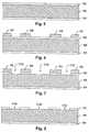
- FIGS. 1 and 2are cross-sections of a wafer-scale optoelectronic package in one embodiment of the invention.
- FIG. 3is a top view of a sub-mount of the optoelectronic package of FIGS. 1 and 2 in one embodiment of the invention.
- FIG. 4is a flowchart of a method for making a lid for the wafer-scale optoelectronic package of FIGS. 1, 2 , and 3 in one embodiment of the invention.
- FIGS. 5, 6 , 7 , 8 , 9 A, 9 B, 10 , 11 , 12 , 13 , 14 , 15 , and 16are the structures formed by the method of FIG. 4 in one embodiment of the invention.
- FIG. 17is a mask used in the method of FIG. 1 in one embodiment of the invention.
- FIG. 18is a flowchart of a method for making a lid for the wafer-scale optoelectronic package of FIGS. 1, 2 , and 3 in another embodiment of the invention.
- FIGS. 19 and 20are the structures formed by the method of FIG. 18 in one embodiment of the invention.
- FIGS. 1, 2 , and 3illustrate a wafer-scale optoelectronic package 150 including a sub-mount 80 and a lid 130 in one embodiment of the invention.
- Sub-mount 80includes an optical lens 52 formed atop a substrate 54 and covered by an oxide layer 56 .
- Buried traces 90 , 92 , 98 , and 100are formed atop oxide layer 56 and covered by a dielectric layer 64 .
- Contact pads 82 , 84 , 86 , and 88are connected by plugs to buried traces 90 , 92 , 98 , and 100 , which are themselves connected by plugs to contact pads 94 , 96 , 102 and 104 (shown in FIG.
- a laser die 122is bonded atop contact pad 82 and wire bonded to contact pad 84
- a monitor photodiode die 124is bonded atop contact pad 86 and wire bonded to contact pad 88 .
- Seal ring 106is connected to contact pads 108 and 110 for grounding purposes.
- Lid 130includes a body 133 that defines a lid cavity 131 having a surface 132 covered by a reflective material 134 .
- Lid cavity 131provides the necessary space to accommodate the dies that are mounted on sub-mount 80 .
- Reflective material 134 on surface 132forms a 45 degree mirror 135 that reflect a light from laser die 122 to lens 52 .
- a seal ring 136is formed on the bond area along the edge of lid 130 around lid cavity 131 .
- Reflective material 134 over lid cavity 131also serves as an EMI shield when it is grounded through seal ring 136 and contact pads 108 and 110 .
- a barrier 322is formed over reflective material 134 to define where seal ring 136 is to be formed. Barrier 322 confines seal ring 136 so the seal ring material (e.g., a solder) does not wick into cavity 131 and interfering with mirror 135 .
- lid 130has a (100) crystallographic plane oriented at a 9.74 degree offset from a major surface 138 .
- Lid 130is anisotropically etched so that surface 132 forms along a (111) crystallographic plane.
- the (100) plane of lid 130is oriented at a 9.74 degree offset from major surface 138
- the (111) plane and mirror 135are oriented at a 45 degree offset from major surface 138 .
- an alignment post 140is bonded to the backside of sub-mount 80 .
- Alignment post 140allows package 150 to be aligned with an optical fiber in a ferrule.
- FIG. 4illustrates a method 200 for forming a wafer-scale lid 130 in one embodiment of the invention.
- nitride layers 302 and 304are formed on the top and the bottom surfaces of a substrate 306 , respectively.
- substrate 306is silicon having a thickness of about 675 microns
- nitride layers 302 and 304are silicon nitride (SiN 4 ) formed by low pressure chemical vapor deposition (LPCVD) and have a thickness of about 1000 to 2000 angstroms.
- nitride layers 302 and 304can be made low stress by modifying the gas ratio (dichlorosilante to ammonia) and the amount of gas flow. In one embodiment, if denser nitride layers 302 and 304 are needed to withstand a KOH etch, nitride layers 302 and 304 can be made silicon rich in order to become denser.
- FIG. 17illustrate a mask 412 used in this lithographic process in one embodiment.
- Mask 412includes lid cavity patterns 414 that define the shape of lid cavity 314 B in FIGS. 9 to 16 .
- lid cavity patterns 414are trapezoidal so that the sidewalls formed by the nonparallel sides are flat instead of stepped.
- Mask 412also includes scribe line patterns 416 that define the separation cavities 314 A and 314 C in FIGS. 9A and 10 to 16 . Scribe line patterns 416 are oriented along a direction on wafer 306 that provides a symmetric etch angle. Note that FIGS. 6 to 9 A and 10 to 16 show the cross-section of the resulting structure formed by method 200 along lines AA′ while FIG. 9B shows the cross-section of the resulting structure formed by method 200 along lines BB′.
- step 206areas of nitride layer 302 exposed by windows 310 A, 310 B, and 310 C in photoresist 308 are etched down to substrate 306 .
- nitride layer 302is etched using a reactive ion etching (RIE) process. The remaining portions of nitride layer 302 serve as a mask for an anisotropic etch.
- RIEreactive ion etching
- step 208as shown in FIG. 8 , resist 308 is stripped. As can be seen, windows 312 A, 312 B, and 312 C are formed in nitride layer 302 . The dimensions of these windows and the space between them are application dependent.
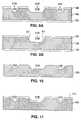
- step 210areas of substrate 306 exposed by windows 312 A to 312 C in nitride layer 302 are etched to form separation cavities 314 A and 314 C, and lid cavity 314 B.
- lid cavity 314 Bhas a 45 degree wall 315 (which corresponds to surface 132 in FIG. 1 ) and a 64.48 degree wall 317 .
- silicon substrate 306is anisotropically etched using a KOH solution having a (100) to (111) plane selectivity of 400 to 1.
- each cavityis etched to 375 microns deep, which results in an undercut of 1 micron in nitride layer 302 due to the selectivity of the etchant.
- nitride layers 302 and 304are removed.
- nitride layers 302 and 304are removed using a hot phosphoric wet etch.
- oxide layer 316is formed over cavities 314 A, 314 B, and 314 C, and on the top surface of substrate 306 .
- oxide layer 316is silicon dioxide that is thermally grown from silicon substrate 306 and has a thickness of about 1000 angstroms.
- a reflective layer 320is formed over oxide layer 316 .
- reflective layer 320is a metal stack of a titanium-platinum-gold (TiPtAu) sequence deposited by e-beam evaporation or sputtering.
- the titanium layerhas a thickness of about 500 angstroms
- the platinum player atop the titanium layerhas a thickness of about 1000 angstroms
- the gold layer atop the titaniumhas a thickness of about 1500 angstroms.
- Metal stack 320is the reflective material 134 ( FIG. 1 ) that forms mirror 135 ( FIG. 1 ) on the (111) plane surface 132 ( FIG. 1 ).
- barrier layer 322is formed over reflective layer 320 .
- barrier layer 322is a metal oxide formed over reflective layer 320 .
- barrier layer 322is a titanium dioxide (TiO 2 ) layer that is thermally deposited upon the TiPtAu metal stack 320 and has a thickness about 500 angstroms.
- barrier layer 322can be a nitride, a boride, a fluoride, a fluorocarbon, a polyimide, or any other material that can withstand the soldering temperatures without adhering to the solder.
- barrier layer 322can be formed by other processes, including sputtering, reactive sputtering, chemical vapor deposition, and plasma enhanced chemical vapor deposition.
- a photoresist 324is next deposited on (e.g., spun on or sprayed on) barrier layer 322 .
- step 224photoresist 324 is exposed and developed to form windows 326 A, 326 B, 326 C, and 326 D. Areas of barrier layer 322 exposed by windows 326 A to 326 D are etched down to reflective layer 320 .
- a titanium dioxide barrier layer 322is etched using a solution of diluted HF (1000:1) and nitric acid (100:1).
- a solderis plated through windows 326 A to 326 D onto reflective layer 320 .
- the solderforms seal ring 136 ( FIGS. 1 and 2 ) on the bond area around lid cavity 314 B (also shown as lid cavity 131 in FIG. 1 ).
- the solderis a gold-tin (AuSn) solder including a gold layer 328 having a thickness of 18,500 angstroms, and a tin layer 330 having a thickness of 18,500 angstroms on top of gold layer 328 .
- photoresist 324is stripped, reapplied, and patterned again to form windows 326 A to 326 D prior to plating the solder.
- step 228as shown in FIG. 16 , photoresist 324 is stripped and lid 130 can now be singulated from adjacent lids 130 (shown partially) along imaginary lines 332 .
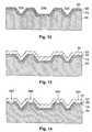
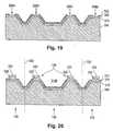
- FIG. 18illustrates a method 400 for forming a wafer-scale lid 130 in another embodiment of the invention. As can be seen, method 400 is similar to method 200 except that steps 426 and 428 have replaced steps 226 and 228 .
- step 426as shown in FIG. 19 , photoresist 324 is stripped. This leaves barrier layer 322 as the mask during the solder plating.
- step 428as shown in FIG. 20 , a solder including gold layer 328 and tin layer 330 are plated through windows 326 A to 326 D (defined now by barrier layer 322 ) onto reflective layer 320 .
- lid 130can be singulated from adjacent lids 130 (shown partially) along imaginary lines 332 .
- photoresist 324is left on as a mask during the solder plating.
- photoresist 324is stripped and barrier layer 322 is used as the mask during the solder plating.
- the advantage of method 400is that photoresist 324 does not have to be a thick resist.
- the uniformity of photoresist coverageis unimportant. Note that the solder and the resulting seal ring 136 will experience a small amount of mushrooming because the solder grows vertically by about the same amount that it grows laterally. In one embodiment, the total plating thickness is about 3 microns so the lateral growth is not problematic.
- TiO 2may be used as the barrier layer.
- TiO 2makes a particularly good barrier layer in the present application for many reasons.
- the AuSn solderwill not adhere to it.
- itadheres well to gold in the metal stack while not many materials do.
- Another advantageis that the methods described require only one mask after the cavity etch. This provides a great cost advantage over other methods that often require up to three masks after the cavity etch.
- TiO 2has been disclosed as a material for the barrier layer, other materials having the following characteristics can also be used: (1) good adherence to the mirror (i.e., the reflective layer); (2) non-wetable to solder; (3) transparent to light; and (4) non-soluble in the plating solution.
- the barrier layerdoes not have to be thin (e.g., less than a quarter wavelength). In some applications, it is advantageous to have a thick barrier layer. As the barrier layer gets to a geometric thickness (angle dependent) near a quarter wave length, substantial changes in reflectance will become evident. These can either be more or less reflective. If the laser is collimated, these interference effects can be exploited to improve the reflectivity of the mirror. However, if the laser is not collimated, the wide range of angles of the light will cause a variable reflectance across the mirror depending on the local angel, resulting in variable intensity of the beam when it leaves the mirror.
Landscapes
- Physics & Mathematics (AREA)
- General Physics & Mathematics (AREA)
- Electromagnetism (AREA)
- Optics & Photonics (AREA)
- Condensed Matter Physics & Semiconductors (AREA)
- Micromachines (AREA)
- Optical Couplings Of Light Guides (AREA)
- Semiconductor Lasers (AREA)
- Optical Elements Other Than Lenses (AREA)
- Physical Vapour Deposition (AREA)
Abstract
Description
- This invention relates to a method for creating a wafer of lids for wafer-scale optoelectronic packages.
- Optoelectronic (OE) devices are generally packaged as individual die. This means of assembly is often slow and labor intensive, resulting in higher product cost. Thus, what is needed is a method to improve the packaging of OE devices.
- In one embodiment of the invention, a method for forming a lid for a wafer-scale package includes (1) forming a cavity in a substrate, (2) forming an oxide layer over the cavity and over a bond area around the cavity on the substrate, (3) forming a reflective layer over the oxide layer, (4) forming a barrier layer over the reflective layer, (5) etching a portion of the barrier layer down to a portion of the reflective layer over the bond area, and (6) forming a solder layer on the portion of the reflective layer. In one embodiment, the reflective layer is a titanium-platinum-gold metal stack and the barrier layer is a titanium dioxide layer.
FIGS. 1 and 2 are cross-sections of a wafer-scale optoelectronic package in one embodiment of the invention.FIG. 3 is a top view of a sub-mount of the optoelectronic package ofFIGS. 1 and 2 in one embodiment of the invention.FIG. 4 is a flowchart of a method for making a lid for the wafer-scale optoelectronic package ofFIGS. 1, 2 , and3 in one embodiment of the invention.FIGS. 5, 6 ,7,8,9A,9B,10,11,12,13,14,15, and16 are the structures formed by the method ofFIG. 4 in one embodiment of the invention.FIG. 17 is a mask used in the method ofFIG. 1 in one embodiment of the invention.FIG. 18 is a flowchart of a method for making a lid for the wafer-scale optoelectronic package ofFIGS. 1, 2 , and3 in another embodiment of the invention.FIGS. 19 and 20 are the structures formed by the method ofFIG. 18 in one embodiment of the invention.- Use of the same reference symbols in different figures indicates similar or identical items. The cross-sectional figures are not drawn to scale and are only for illustrative purposes.
FIGS. 1, 2 , and3 illustrate a wafer-scaleoptoelectronic package 150 including asub-mount 80 and alid 130 in one embodiment of the invention.Sub-mount 80 includes anoptical lens 52 formed atop asubstrate 54 and covered by anoxide layer 56. Buriedtraces oxide layer 56 and covered by adielectric layer 64.Contact pads FIG. 3 ) are connected by plugs to buriedtraces contact pads FIG. 3 ) located outside of aseal ring 106. A laser die122 is bonded atopcontact pad 82 and wire bonded to contactpad 84, and a monitor photodiode die124 is bonded atopcontact pad 86 and wire bonded to contactpad 88.Seal ring 106 is connected tocontact pads Lid 130 includes abody 133 that defines alid cavity 131 having asurface 132 covered by areflective material 134.Lid cavity 131 provides the necessary space to accommodate the dies that are mounted onsub-mount 80.Reflective material 134 onsurface 132 forms a 45degree mirror 135 that reflect a light fromlaser die 122 tolens 52. Aseal ring 136 is formed on the bond area along the edge oflid 130 aroundlid cavity 131.Reflective material 134 overlid cavity 131 also serves as an EMI shield when it is grounded throughseal ring 136 andcontact pads barrier 322 is formed overreflective material 134 to define whereseal ring 136 is to be formed.Barrier 322confines seal ring 136 so the seal ring material (e.g., a solder) does not wick intocavity 131 and interfering withmirror 135.- In one embodiment,
lid 130 has a (100) crystallographic plane oriented at a 9.74 degree offset from amajor surface 138.Lid 130 is anisotropically etched so thatsurface 132 forms along a (111) crystallographic plane. As the (100) plane oflid 130 is oriented at a 9.74 degree offset frommajor surface 138, the (111) plane andmirror 135 are oriented at a 45 degree offset frommajor surface 138. - In one embodiment, an
alignment post 140 is bonded to the backside ofsub-mount 80.Alignment post 140 allowspackage 150 to be aligned with an optical fiber in a ferrule. FIG. 4 illustrates amethod 200 for forming a wafer-scale lid 130 in one embodiment of the invention.- In
step 202, as shown inFIG. 5 ,nitride layers substrate 306, respectively. In one embodiment,substrate 306 is silicon having a thickness of about 675 microns, andnitride layers nitride layers silicon substrate 306 becomes problematic,nitride layers denser nitride layers nitride layers - In
step 204, as shown inFIG. 6 , aphotoresist 308 is next spun, exposed, and developed onnitride layer 302.FIG. 17 illustrate amask 412 used in this lithographic process in one embodiment.Mask 412 includeslid cavity patterns 414 that define the shape oflid cavity 314B in FIGS.9 to16. In one embodiment,lid cavity patterns 414 are trapezoidal so that the sidewalls formed by the nonparallel sides are flat instead of stepped.Mask 412 also includesscribe line patterns 416 that define theseparation cavities FIGS. 9A and 10 to16. Scribeline patterns 416 are oriented along a direction onwafer 306 that provides a symmetric etch angle. Note that FIGS.6 to9A and10 to16 show the cross-section of the resulting structure formed bymethod 200 along lines AA′ whileFIG. 9B shows the cross-section of the resulting structure formed bymethod 200 along lines BB′. - In
step 206, as shown inFIG. 7 , areas ofnitride layer 302 exposed bywindows photoresist 308 are etched down tosubstrate 306. In one embodiment,nitride layer 302 is etched using a reactive ion etching (RIE) process. The remaining portions ofnitride layer 302 serve as a mask for an anisotropic etch. - In
step 208, as shown inFIG. 8 ,resist 308 is stripped. As can be seen,windows nitride layer 302. The dimensions of these windows and the space between them are application dependent. - In
step 210, as shown inFIG. 9A along line AA′ and inFIG. 9B along line BB′, areas ofsubstrate 306 exposed bywindows 312A to312C innitride layer 302 are etched to formseparation cavities lid cavity 314B. As can be seen inFIG. 9B ,lid cavity 314B has a 45 degree wall315 (which corresponds tosurface 132 inFIG. 1 ) and a 64.48degree wall 317. In one embodiment,silicon substrate 306 is anisotropically etched using a KOH solution having a (100) to (111) plane selectivity of 400 to 1. In one embodiment, each cavity is etched to 375 microns deep, which results in an undercut of 1 micron innitride layer 302 due to the selectivity of the etchant. - In
step 214, as shown inFIG. 10 , nitride layers302 and304 are removed. In one embodiment, nitride layers302 and304 are removed using a hot phosphoric wet etch. - In
step 216, as shown inFIG. 11 , anoxide layer 316 is formed overcavities substrate 306. In one embodiment,oxide layer 316 is silicon dioxide that is thermally grown fromsilicon substrate 306 and has a thickness of about 1000 angstroms. - In
step 218, as shown inFIG. 12 , areflective layer 320 is formed overoxide layer 316. In one embodiment,reflective layer 320 is a metal stack of a titanium-platinum-gold (TiPtAu) sequence deposited by e-beam evaporation or sputtering. In one embodiment, the titanium layer has a thickness of about 500 angstroms, the platinum player atop the titanium layer has a thickness of about 1000 angstroms, and the gold layer atop the titanium has a thickness of about 1500 angstroms.Metal stack 320 is the reflective material134 (FIG. 1 ) that forms mirror135 (FIG. 1 ) on the (111) plane surface132 (FIG. 1 ). - In
step 220, as shown inFIG. 12 , abarrier layer 322 is formed overreflective layer 320. In one embodiment,barrier layer 322 is a metal oxide formed overreflective layer 320. For example,barrier layer 322 is a titanium dioxide (TiO2) layer that is thermally deposited upon theTiPtAu metal stack 320 and has a thickness about 500 angstroms. Alternatively,barrier layer 322 can be a nitride, a boride, a fluoride, a fluorocarbon, a polyimide, or any other material that can withstand the soldering temperatures without adhering to the solder. Furthermore,barrier layer 322 can be formed by other processes, including sputtering, reactive sputtering, chemical vapor deposition, and plasma enhanced chemical vapor deposition. - In
step 222, as shown inFIG. 13 , aphotoresist 324 is next deposited on (e.g., spun on or sprayed on)barrier layer 322. - In
step 224, as shown inFIG. 14 ,photoresist 324 is exposed and developed to formwindows barrier layer 322 exposed bywindows 326A to326D are etched down toreflective layer 320. In one embodiment, a titaniumdioxide barrier layer 322 is etched using a solution of diluted HF (1000:1) and nitric acid (100:1). - In
step 226, as shown inFIG. 15 , a solder is plated throughwindows 326A to326D ontoreflective layer 320. The solder forms seal ring136 (FIGS. 1 and 2 ) on the bond area aroundlid cavity 314B (also shown aslid cavity 131 inFIG. 1 ). In one embodiment, the solder is a gold-tin (AuSn) solder including agold layer 328 having a thickness of 18,500 angstroms, and atin layer 330 having a thickness of 18,500 angstroms on top ofgold layer 328. In one embodiment,photoresist 324 is stripped, reapplied, and patterned again to formwindows 326A to326D prior to plating the solder. This is because the gold plating (on the bottom) may mushroom over the top of the initial resist for gold plating. Therefore, in order to get somewhat vertical edges, it may be necessary to remove the original resist and reapply a thicker resist that will provide a form for the solder plating. - In
step 228, as shown inFIG. 16 ,photoresist 324 is stripped andlid 130 can now be singulated from adjacent lids130 (shown partially) alongimaginary lines 332. FIG. 18 illustrates amethod 400 for forming a wafer-scale lid 130 in another embodiment of the invention. As can be seen,method 400 is similar tomethod 200 except that steps426 and428 have replacedsteps - In
step 426, as shown inFIG. 19 ,photoresist 324 is stripped. This leavesbarrier layer 322 as the mask during the solder plating. - In
step 428, as shown inFIG. 20 , a solder includinggold layer 328 andtin layer 330 are plated throughwindows 326A to326D (defined now by barrier layer322) ontoreflective layer 320. Again,lid 130 can be singulated from adjacent lids130 (shown partially) alongimaginary lines 332. - In
method 200,photoresist 324 is left on as a mask during the solder plating. Inmethod 400,photoresist 324 is stripped andbarrier layer 322 is used as the mask during the solder plating. The advantage ofmethod 400 is thatphotoresist 324 does not have to be a thick resist. In addition, the uniformity of photoresist coverage is unimportant. Note that the solder and the resultingseal ring 136 will experience a small amount of mushrooming because the solder grows vertically by about the same amount that it grows laterally. In one embodiment, the total plating thickness is about 3 microns so the lateral growth is not problematic. - As described above, TiO2may be used as the barrier layer. TiO2makes a particularly good barrier layer in the present application for many reasons. First, the AuSn solder will not adhere to it. Second, it adheres well to gold in the metal stack while not many materials do. Third, although it has a high refractive index, which can alter the reflective of the gold, it is possible to deposit a very thin layer (e.g., much less than a quarter wavelength). At this thickness, there should be little effect on light transmission through the lid. Another advantage is that the methods described require only one mask after the cavity etch. This provides a great cost advantage over other methods that often require up to three masks after the cavity etch.
- Although TiO2has been disclosed as a material for the barrier layer, other materials having the following characteristics can also be used: (1) good adherence to the mirror (i.e., the reflective layer); (2) non-wetable to solder; (3) transparent to light; and (4) non-soluble in the plating solution.
- Furthermore, the barrier layer does not have to be thin (e.g., less than a quarter wavelength). In some applications, it is advantageous to have a thick barrier layer. As the barrier layer gets to a geometric thickness (angle dependent) near a quarter wave length, substantial changes in reflectance will become evident. These can either be more or less reflective. If the laser is collimated, these interference effects can be exploited to improve the reflectivity of the mirror. However, if the laser is not collimated, the wide range of angles of the light will cause a variable reflectance across the mirror depending on the local angel, resulting in variable intensity of the beam when it leaves the mirror.
- Various other adaptations and combinations of features of the embodiments disclosed are within the scope of the invention. Numerous embodiments are encompassed by the following claims.
Claims (21)
Priority Applications (1)
| Application Number | Priority Date | Filing Date | Title |
|---|---|---|---|
| US11/097,534US7534636B2 (en) | 2004-06-24 | 2005-03-31 | Lids for wafer-scale optoelectronic packages |
Applications Claiming Priority (2)
| Application Number | Priority Date | Filing Date | Title |
|---|---|---|---|
| US10/877,615US7045827B2 (en) | 2004-06-24 | 2004-06-24 | Lids for wafer-scale optoelectronic packages |
| US11/097,534US7534636B2 (en) | 2004-06-24 | 2005-03-31 | Lids for wafer-scale optoelectronic packages |
Related Parent Applications (1)
| Application Number | Title | Priority Date | Filing Date |
|---|---|---|---|
| US10/877,615DivisionUS7045827B2 (en) | 2004-06-24 | 2004-06-24 | Lids for wafer-scale optoelectronic packages |
Publications (2)
| Publication Number | Publication Date |
|---|---|
| US20050285131A1true US20050285131A1 (en) | 2005-12-29 |
| US7534636B2 US7534636B2 (en) | 2009-05-19 |
Family
ID=35504672
Family Applications (3)
| Application Number | Title | Priority Date | Filing Date |
|---|---|---|---|
| US10/877,615Expired - LifetimeUS7045827B2 (en) | 2004-06-24 | 2004-06-24 | Lids for wafer-scale optoelectronic packages |
| US11/097,534Expired - Fee RelatedUS7534636B2 (en) | 2004-06-24 | 2005-03-31 | Lids for wafer-scale optoelectronic packages |
| US11/335,091AbandonedUS20060121635A1 (en) | 2004-06-24 | 2006-01-18 | Lids for wafer-scale optoelectronic packages |
Family Applications Before (1)
| Application Number | Title | Priority Date | Filing Date |
|---|---|---|---|
| US10/877,615Expired - LifetimeUS7045827B2 (en) | 2004-06-24 | 2004-06-24 | Lids for wafer-scale optoelectronic packages |
Family Applications After (1)
| Application Number | Title | Priority Date | Filing Date |
|---|---|---|---|
| US11/335,091AbandonedUS20060121635A1 (en) | 2004-06-24 | 2006-01-18 | Lids for wafer-scale optoelectronic packages |
Country Status (4)
| Country | Link |
|---|---|
| US (3) | US7045827B2 (en) |
| JP (1) | JP4869634B2 (en) |
| CN (1) | CN1713468B (en) |
| DE (1) | DE102005010926B4 (en) |
Cited By (7)
| Publication number | Priority date | Publication date | Assignee | Title |
|---|---|---|---|---|
| US20060252167A1 (en)* | 2005-05-04 | 2006-11-09 | Wang Tak K | Silicon optical package with 45 degree turning mirror |
| US8315287B1 (en) | 2011-05-03 | 2012-11-20 | Avago Technologies Fiber Ip (Singapore) Pte. Ltd | Surface-emitting semiconductor laser device in which an edge-emitting laser is integrated with a diffractive lens, and a method for making the device |
| WO2013096169A1 (en)* | 2011-12-22 | 2013-06-27 | 3M Innovative Properties Company | Optical device with sensor and method of making and using same |
| US8582618B2 (en) | 2011-01-18 | 2013-11-12 | Avago Technologies General Ip (Singapore) Pte. Ltd. | Surface-emitting semiconductor laser device in which an edge-emitting laser is integrated with a diffractive or refractive lens on the semiconductor laser device |
| US9793237B2 (en) | 2015-10-19 | 2017-10-17 | Qorvo Us, Inc. | Hollow-cavity flip-chip package with reinforced interconnects and process for making the same |
| US9799637B2 (en)* | 2016-02-12 | 2017-10-24 | Qorvo Us, Inc. | Semiconductor package with lid having lid conductive structure |
| WO2018185032A1 (en)* | 2017-04-03 | 2018-10-11 | Indigo Diabetes N.V. | Implantable optical sensor with hermetically sealed cover cap |
Families Citing this family (10)
| Publication number | Priority date | Publication date | Assignee | Title |
|---|---|---|---|---|
| CN100559559C (en)* | 2007-03-08 | 2009-11-11 | 探微科技股份有限公司 | Method for manufacturing optical element sealing cover |
| JP2009032843A (en)* | 2007-07-26 | 2009-02-12 | Nec Electronics Corp | Semiconductor device and manufacturing method therefor |
| US20100032702A1 (en)* | 2008-08-11 | 2010-02-11 | E. I. Du Pont De Nemours And Company | Light-Emitting Diode Housing Comprising Fluoropolymer |
| CN101599522B (en)* | 2009-06-30 | 2011-05-25 | 厦门市三安光电科技有限公司 | Vertical LED adopting insulating medium barrier layer and preparation method thereof |
| JP2011222675A (en)* | 2010-04-07 | 2011-11-04 | Mitsubishi Electric Corp | Semiconductor device and method of manufacturing the same |
| DE102012217793A1 (en)* | 2012-09-28 | 2014-04-03 | Fraunhofer-Gesellschaft zur Förderung der angewandten Forschung e.V. | PRODUCTION METHOD |
| JP2014158157A (en)* | 2013-02-15 | 2014-08-28 | Asahi Kasei Electronics Co Ltd | Piezoelectric device |
| NO2944700T3 (en)* | 2013-07-11 | 2018-03-17 | ||
| US10242967B2 (en) | 2017-05-16 | 2019-03-26 | Raytheon Company | Die encapsulation in oxide bonded wafer stack |
| JP6970336B2 (en)* | 2017-08-04 | 2021-11-24 | 日亜化学工業株式会社 | Light source device |
Citations (16)
| Publication number | Priority date | Publication date | Assignee | Title |
|---|---|---|---|---|
| US3657029A (en)* | 1968-12-31 | 1972-04-18 | Texas Instruments Inc | Platinum thin-film metallization method |
| US4773972A (en)* | 1986-10-30 | 1988-09-27 | Ford Motor Company | Method of making silicon capacitive pressure sensor with glass layer between silicon wafers |
| US4791075A (en)* | 1987-10-05 | 1988-12-13 | Motorola, Inc. | Process for making a hermetic low cost pin grid array package |
| US5336928A (en)* | 1992-09-18 | 1994-08-09 | General Electric Company | Hermetically sealed packaged electronic system |
| US5500540A (en)* | 1994-04-15 | 1996-03-19 | Photonics Research Incorporated | Wafer scale optoelectronic package |
| US6062461A (en)* | 1998-06-03 | 2000-05-16 | Delphi Technologies, Inc. | Process for bonding micromachined wafers using solder |
| US6130107A (en)* | 1997-08-28 | 2000-10-10 | Lucent Technologies Inc. | Corrosion protection in the fabrication of optoelectronic assemblies |
| US6487224B1 (en)* | 1998-09-30 | 2002-11-26 | Kabushiki Kaisha Toshiba | Laser diode assembly |
| US20030071283A1 (en)* | 2001-10-17 | 2003-04-17 | Hymite A/S | Semiconductor structure with one or more through-holes |
| US6696645B2 (en)* | 2002-05-08 | 2004-02-24 | The Regents Of The University Of Michigan | On-wafer packaging for RF-MEMS |
| US20040087043A1 (en)* | 2001-10-30 | 2004-05-06 | Asia Pacific Microsystems, Inc. | Package structure and method for making the same |
| US20050063648A1 (en)* | 2003-09-19 | 2005-03-24 | Wilson Robert Edward | Alignment post for optical subassemblies made with cylindrical rods, tubes, spheres, or similar features |
| US20050111797A1 (en)* | 2003-09-15 | 2005-05-26 | Rohm And Haas Electronic Materials, L.L.C. | Device package and methods for the fabrication and testing thereof |
| US20050124159A1 (en)* | 2002-02-14 | 2005-06-09 | Edvard Kalvesten | Deflectable microstructure and method of manufacturing the same through bonding of wafers |
| US20050265722A1 (en)* | 2003-09-19 | 2005-12-01 | Gallup Kendra J | Integrated optics and electronics |
| US20070228576A1 (en)* | 2005-06-14 | 2007-10-04 | John Trezza | Isolating chip-to-chip contact |
Family Cites Families (4)
| Publication number | Priority date | Publication date | Assignee | Title |
|---|---|---|---|---|
| JPH01264285A (en)* | 1988-04-15 | 1989-10-20 | Omron Tateisi Electron Co | Surface light-emitting type semiconductor laser |
| DE4440935A1 (en)* | 1994-11-17 | 1996-05-23 | Ant Nachrichtentech | Optical transmitting and receiving device |
| JP2000019357A (en)* | 1998-06-30 | 2000-01-21 | Toshiba Corp | Optical array module and reflector array |
| DE19845484C2 (en)* | 1998-10-02 | 2002-09-26 | Infineon Technologies Ag | Micro-optical component and method for its production |
- 2004
- 2004-06-24USUS10/877,615patent/US7045827B2/ennot_activeExpired - Lifetime
- 2005
- 2005-03-09DEDE102005010926Apatent/DE102005010926B4/ennot_activeExpired - Fee Related
- 2005-03-31USUS11/097,534patent/US7534636B2/ennot_activeExpired - Fee Related
- 2005-04-01CNCN2005100598904Apatent/CN1713468B/ennot_activeExpired - Fee Related
- 2005-06-03JPJP2005163977Apatent/JP4869634B2/ennot_activeExpired - Fee Related
- 2006
- 2006-01-18USUS11/335,091patent/US20060121635A1/ennot_activeAbandoned
Patent Citations (16)
| Publication number | Priority date | Publication date | Assignee | Title |
|---|---|---|---|---|
| US3657029A (en)* | 1968-12-31 | 1972-04-18 | Texas Instruments Inc | Platinum thin-film metallization method |
| US4773972A (en)* | 1986-10-30 | 1988-09-27 | Ford Motor Company | Method of making silicon capacitive pressure sensor with glass layer between silicon wafers |
| US4791075A (en)* | 1987-10-05 | 1988-12-13 | Motorola, Inc. | Process for making a hermetic low cost pin grid array package |
| US5336928A (en)* | 1992-09-18 | 1994-08-09 | General Electric Company | Hermetically sealed packaged electronic system |
| US5500540A (en)* | 1994-04-15 | 1996-03-19 | Photonics Research Incorporated | Wafer scale optoelectronic package |
| US6130107A (en)* | 1997-08-28 | 2000-10-10 | Lucent Technologies Inc. | Corrosion protection in the fabrication of optoelectronic assemblies |
| US6062461A (en)* | 1998-06-03 | 2000-05-16 | Delphi Technologies, Inc. | Process for bonding micromachined wafers using solder |
| US6487224B1 (en)* | 1998-09-30 | 2002-11-26 | Kabushiki Kaisha Toshiba | Laser diode assembly |
| US20030071283A1 (en)* | 2001-10-17 | 2003-04-17 | Hymite A/S | Semiconductor structure with one or more through-holes |
| US20040087043A1 (en)* | 2001-10-30 | 2004-05-06 | Asia Pacific Microsystems, Inc. | Package structure and method for making the same |
| US20050124159A1 (en)* | 2002-02-14 | 2005-06-09 | Edvard Kalvesten | Deflectable microstructure and method of manufacturing the same through bonding of wafers |
| US6696645B2 (en)* | 2002-05-08 | 2004-02-24 | The Regents Of The University Of Michigan | On-wafer packaging for RF-MEMS |
| US20050111797A1 (en)* | 2003-09-15 | 2005-05-26 | Rohm And Haas Electronic Materials, L.L.C. | Device package and methods for the fabrication and testing thereof |
| US20050063648A1 (en)* | 2003-09-19 | 2005-03-24 | Wilson Robert Edward | Alignment post for optical subassemblies made with cylindrical rods, tubes, spheres, or similar features |
| US20050265722A1 (en)* | 2003-09-19 | 2005-12-01 | Gallup Kendra J | Integrated optics and electronics |
| US20070228576A1 (en)* | 2005-06-14 | 2007-10-04 | John Trezza | Isolating chip-to-chip contact |
Cited By (14)
| Publication number | Priority date | Publication date | Assignee | Title |
|---|---|---|---|---|
| US7750356B2 (en)* | 2005-05-04 | 2010-07-06 | Avago Technologies Fiber Ip (Singapore) Pte. Ltd. | Silicon optical package with 45 degree turning mirror |
| US20100226406A1 (en)* | 2005-05-04 | 2010-09-09 | Avago Technologies Fiber Ip (Singapore) Pte. Ltd. | Silicon optical package with 45 degree turning mirror |
| US20060252167A1 (en)* | 2005-05-04 | 2006-11-09 | Wang Tak K | Silicon optical package with 45 degree turning mirror |
| US8582618B2 (en) | 2011-01-18 | 2013-11-12 | Avago Technologies General Ip (Singapore) Pte. Ltd. | Surface-emitting semiconductor laser device in which an edge-emitting laser is integrated with a diffractive or refractive lens on the semiconductor laser device |
| US8315287B1 (en) | 2011-05-03 | 2012-11-20 | Avago Technologies Fiber Ip (Singapore) Pte. Ltd | Surface-emitting semiconductor laser device in which an edge-emitting laser is integrated with a diffractive lens, and a method for making the device |
| CN104094143A (en)* | 2011-12-22 | 2014-10-08 | 3M创新有限公司 | Optical Device With Sensor And Method Of Making And Using Same |
| WO2013096169A1 (en)* | 2011-12-22 | 2013-06-27 | 3M Innovative Properties Company | Optical device with sensor and method of making and using same |
| US9423297B2 (en) | 2011-12-22 | 2016-08-23 | 3M Innovative Properties Company | Optical device with optical element and sensor for sampling light |
| US9793237B2 (en) | 2015-10-19 | 2017-10-17 | Qorvo Us, Inc. | Hollow-cavity flip-chip package with reinforced interconnects and process for making the same |
| US9799637B2 (en)* | 2016-02-12 | 2017-10-24 | Qorvo Us, Inc. | Semiconductor package with lid having lid conductive structure |
| WO2018185032A1 (en)* | 2017-04-03 | 2018-10-11 | Indigo Diabetes N.V. | Implantable optical sensor with hermetically sealed cover cap |
| CN110709743A (en)* | 2017-04-03 | 2020-01-17 | 英迪格迪贝特斯公司 | Implantable optical sensor with hermetically sealed cover |
| EP3607368A1 (en)* | 2017-04-03 | 2020-02-12 | Indigo Diabetes N.V. | Implantable optical sensor with hermetically sealed cover cap |
| US11372176B2 (en) | 2017-04-03 | 2022-06-28 | Indigo Diabetes N.V. | Implantable optical sensor with hermetically sealed cover cap |
Also Published As
| Publication number | Publication date |
|---|---|
| DE102005010926B4 (en) | 2008-05-08 |
| JP2006013484A (en) | 2006-01-12 |
| JP4869634B2 (en) | 2012-02-08 |
| US20050285242A1 (en) | 2005-12-29 |
| DE102005010926A1 (en) | 2006-03-30 |
| US7534636B2 (en) | 2009-05-19 |
| US20060121635A1 (en) | 2006-06-08 |
| US7045827B2 (en) | 2006-05-16 |
| CN1713468A (en) | 2005-12-28 |
| CN1713468B (en) | 2011-10-05 |
Similar Documents
| Publication | Publication Date | Title |
|---|---|---|
| US20060121635A1 (en) | Lids for wafer-scale optoelectronic packages | |
| US12276816B2 (en) | Wafer level microstructures for an optical lens | |
| US20190384002A1 (en) | Stepped optical bridge for connecting semiconductor waveguides | |
| US5853960A (en) | Method for producing a micro optical semiconductor lens | |
| US6122109A (en) | Non-planar micro-optical structures | |
| US6289030B1 (en) | Fabrication of semiconductor devices | |
| US20240128403A1 (en) | Micro light emitting element and its preparation method | |
| US6810189B2 (en) | Optical waveguide and method for preparing the same | |
| EP1854189A2 (en) | High reliability etched-facet photonic devices | |
| KR0172797B1 (en) | Laser diode and manufacturing method thereof | |
| JP2008505355A (en) | Method for manufacturing an optical waveguide assembly having an integral alignment mechanism | |
| US6596185B2 (en) | Formation of optical components on a substrate | |
| US20020110341A1 (en) | Manufacturing method for edge-emitting or edge-coupled waveguide optoelectronic devices | |
| US6920267B2 (en) | Optical coupling device and manufacturing method thereof | |
| US11001535B2 (en) | Transferring nanostructures from wafers to transparent substrates | |
| CN116325388A (en) | Formation of semiconductor devices for non-hermetic environments | |
| CN120527755A (en) | Electroabsorption modulation semiconductor laser and preparation method thereof | |
| JP5264764B2 (en) | Etched facet ridge laser with etch stop | |
| CN117239539A (en) | A high-speed chip with high reliability and its manufacturing process | |
| JPH0621039A (en) | Thin-film taper formation method | |
| JPS62211980A (en) | Manufacturing method of semiconductor laser device | |
| US20140272315A1 (en) | Method for fabricating negative photoresist etched pits and trenches as controlled optical path and a device fabricated thereby | |
| JPS62115792A (en) | Semiconductor laser | |
| JPH02312291A (en) | Manufacture of semiconductor laser |
Legal Events
| Date | Code | Title | Description |
|---|---|---|---|
| AS | Assignment | Owner name:AVAGO TECHNOLOGIES GENERAL IP PTE. LTD.,SINGAPORE Free format text:ASSIGNMENT OF ASSIGNORS INTEREST;ASSIGNOR:AGILENT TECHNOLOGIES, INC.;REEL/FRAME:017206/0666 Effective date:20051201 Owner name:AVAGO TECHNOLOGIES GENERAL IP PTE. LTD., SINGAPORE Free format text:ASSIGNMENT OF ASSIGNORS INTEREST;ASSIGNOR:AGILENT TECHNOLOGIES, INC.;REEL/FRAME:017206/0666 Effective date:20051201 | |
| AS | Assignment | Owner name:AVAGO TECHNOLOGIES FIBER IP (SINGAPORE) PTE. LTD., Free format text:ASSIGNMENT OF ASSIGNORS INTEREST;ASSIGNOR:AVAGO TECHNOLOGIES GENERAL IP (SINGAPORE) PTE. LTD.;REEL/FRAME:017675/0294 Effective date:20051201 | |
| STCF | Information on status: patent grant | Free format text:PATENTED CASE | |
| CC | Certificate of correction | ||
| FPAY | Fee payment | Year of fee payment:4 | |
| AS | Assignment | Owner name:DEUTSCHE BANK AG NEW YORK BRANCH, AS COLLATERAL AGENT, NEW YORK Free format text:PATENT SECURITY AGREEMENT;ASSIGNOR:AVAGO TECHNOLOGIES GENERAL IP (SINGAPORE) PTE. LTD.;REEL/FRAME:032851/0001 Effective date:20140506 Owner name:DEUTSCHE BANK AG NEW YORK BRANCH, AS COLLATERAL AG Free format text:PATENT SECURITY AGREEMENT;ASSIGNOR:AVAGO TECHNOLOGIES GENERAL IP (SINGAPORE) PTE. LTD.;REEL/FRAME:032851/0001 Effective date:20140506 | |
| AS | Assignment | Owner name:AVAGO TECHNOLOGIES GENERAL IP (SINGAPORE) PTE. LTD., SINGAPORE Free format text:TERMINATION AND RELEASE OF SECURITY INTEREST IN PATENT RIGHTS (RELEASES RF 032851-0001);ASSIGNOR:DEUTSCHE BANK AG NEW YORK BRANCH, AS COLLATERAL AGENT;REEL/FRAME:037689/0001 Effective date:20160201 Owner name:AVAGO TECHNOLOGIES GENERAL IP (SINGAPORE) PTE. LTD Free format text:TERMINATION AND RELEASE OF SECURITY INTEREST IN PATENT RIGHTS (RELEASES RF 032851-0001);ASSIGNOR:DEUTSCHE BANK AG NEW YORK BRANCH, AS COLLATERAL AGENT;REEL/FRAME:037689/0001 Effective date:20160201 | |
| AS | Assignment | Owner name:BANK OF AMERICA, N.A., AS COLLATERAL AGENT, NORTH CAROLINA Free format text:PATENT SECURITY AGREEMENT;ASSIGNOR:AVAGO TECHNOLOGIES GENERAL IP (SINGAPORE) PTE. LTD.;REEL/FRAME:037808/0001 Effective date:20160201 Owner name:BANK OF AMERICA, N.A., AS COLLATERAL AGENT, NORTH Free format text:PATENT SECURITY AGREEMENT;ASSIGNOR:AVAGO TECHNOLOGIES GENERAL IP (SINGAPORE) PTE. LTD.;REEL/FRAME:037808/0001 Effective date:20160201 | |
| AS | Assignment | Owner name:AVAGO TECHNOLOGIES GENERAL IP (SINGAPORE) PTE. LTD Free format text:CORRECTIVE ASSIGNMENT TO CORRECT THE ASSIGNEE NAME PREVIOUSLY RECORDED AT REEL: 017206 FRAME: 0666. ASSIGNOR(S) HEREBY CONFIRMS THE ASSIGNMENT;ASSIGNOR:AGILENT TECHNOLOGIES, INC.;REEL/FRAME:038632/0662 Effective date:20051201 | |
| FPAY | Fee payment | Year of fee payment:8 | |
| AS | Assignment | Owner name:AVAGO TECHNOLOGIES GENERAL IP (SINGAPORE) PTE. LTD., SINGAPORE Free format text:TERMINATION AND RELEASE OF SECURITY INTEREST IN PATENTS;ASSIGNOR:BANK OF AMERICA, N.A., AS COLLATERAL AGENT;REEL/FRAME:041710/0001 Effective date:20170119 Owner name:AVAGO TECHNOLOGIES GENERAL IP (SINGAPORE) PTE. LTD Free format text:TERMINATION AND RELEASE OF SECURITY INTEREST IN PATENTS;ASSIGNOR:BANK OF AMERICA, N.A., AS COLLATERAL AGENT;REEL/FRAME:041710/0001 Effective date:20170119 | |
| AS | Assignment | Owner name:AVAGO TECHNOLOGIES INTERNATIONAL SALES PTE. LIMITE Free format text:MERGER;ASSIGNOR:AVAGO TECHNOLOGIES GENERAL IP (SINGAPORE) PTE. LTD.;REEL/FRAME:047195/0827 Effective date:20180509 | |
| AS | Assignment | Owner name:AVAGO TECHNOLOGIES INTERNATIONAL SALES PTE. LIMITE Free format text:CORRECTIVE ASSIGNMENT TO CORRECT THE EFFECTIVE DATE OF MERGER PREVIOUSLY RECORDED AT REEL: 047195 FRAME: 0827. ASSIGNOR(S) HEREBY CONFIRMS THE MERGER;ASSIGNOR:AVAGO TECHNOLOGIES GENERAL IP (SINGAPORE) PTE. LTD.;REEL/FRAME:047924/0571 Effective date:20180905 | |
| AS | Assignment | Owner name:BROADCOM INTERNATIONAL PTE. LTD., SINGAPORE Free format text:ASSIGNMENT OF ASSIGNORS INTEREST;ASSIGNOR:AVAGO TECHNOLOGIES INTERNATIONAL SALES PTE. LIMITED;REEL/FRAME:053771/0901 Effective date:20200826 | |
| FEPP | Fee payment procedure | Free format text:MAINTENANCE FEE REMINDER MAILED (ORIGINAL EVENT CODE: REM.); ENTITY STATUS OF PATENT OWNER: LARGE ENTITY | |
| LAPS | Lapse for failure to pay maintenance fees | Free format text:PATENT EXPIRED FOR FAILURE TO PAY MAINTENANCE FEES (ORIGINAL EVENT CODE: EXP.); ENTITY STATUS OF PATENT OWNER: LARGE ENTITY | |
| STCH | Information on status: patent discontinuation | Free format text:PATENT EXPIRED DUE TO NONPAYMENT OF MAINTENANCE FEES UNDER 37 CFR 1.362 | |
| FP | Lapsed due to failure to pay maintenance fee | Effective date:20210519 |