US20050284570A1 - Diagnostic plasma measurement device having patterned sensors and features - Google Patents
Diagnostic plasma measurement device having patterned sensors and featuresDownload PDFInfo
- Publication number
- US20050284570A1 US20050284570A1US10/875,954US87595404AUS2005284570A1US 20050284570 A1US20050284570 A1US 20050284570A1US 87595404 AUS87595404 AUS 87595404AUS 2005284570 A1US2005284570 A1US 2005284570A1
- Authority
- US
- United States
- Prior art keywords
- plasma
- sensor
- fields
- measurement probe
- disposed
- Prior art date
- Legal status (The legal status is an assumption and is not a legal conclusion. Google has not performed a legal analysis and makes no representation as to the accuracy of the status listed.)
- Abandoned
Links
- 238000005259measurementMethods0.000titleclaimsabstractdescription61
- 239000000523sampleSubstances0.000claimsabstractdescription162
- 238000012545processingMethods0.000claimsabstractdescription71
- 238000000034methodMethods0.000claimsabstractdescription66
- 238000012546transferMethods0.000claimsabstractdescription58
- 239000000758substrateSubstances0.000claimsabstractdescription54
- 238000004891communicationMethods0.000claimsabstractdescription35
- 230000008569processEffects0.000claimsdescription19
- 238000007667floatingMethods0.000claimsdescription9
- 238000006243chemical reactionMethods0.000claimsdescription8
- 230000009977dual effectEffects0.000claimsdescription6
- 238000004519manufacturing processMethods0.000abstractdescription27
- 238000011109contaminationMethods0.000abstractdescription4
- 238000000206photolithographyMethods0.000abstractdescription4
- 210000002381plasmaAnatomy0.000description97
- 235000012431wafersNutrition0.000description95
- 210000004027cellAnatomy0.000description14
- 230000037361pathwayEffects0.000description10
- 239000004065semiconductorSubstances0.000description10
- 238000003491arrayMethods0.000description9
- 239000007789gasSubstances0.000description8
- XUIMIQQOPSSXEZ-UHFFFAOYSA-NSiliconChemical compound[Si]XUIMIQQOPSSXEZ-UHFFFAOYSA-N0.000description7
- 230000006870functionEffects0.000description7
- 229910052710siliconInorganic materials0.000description7
- 239000010703siliconSubstances0.000description7
- 238000011065in-situ storageMethods0.000description6
- 229910052751metalInorganic materials0.000description6
- 239000002184metalSubstances0.000description6
- 238000005516engineering processMethods0.000description5
- 238000002161passivationMethods0.000description5
- 238000003860storageMethods0.000description5
- 229910052782aluminiumInorganic materials0.000description4
- XAGFODPZIPBFFR-UHFFFAOYSA-NaluminiumChemical compound[Al]XAGFODPZIPBFFR-UHFFFAOYSA-N0.000description4
- 238000013459approachMethods0.000description4
- 238000005260corrosionMethods0.000description4
- 230000007797corrosionEffects0.000description4
- 238000013461designMethods0.000description4
- 238000002955isolationMethods0.000description4
- 238000001459lithographyMethods0.000description4
- 229920002120photoresistant polymerPolymers0.000description4
- 239000004020conductorSubstances0.000description3
- 238000005530etchingMethods0.000description3
- 230000004907fluxEffects0.000description3
- 239000000463materialSubstances0.000description3
- 230000003287optical effectEffects0.000description3
- 238000000059patterningMethods0.000description3
- 238000005070samplingMethods0.000description3
- VYPSYNLAJGMNEJ-UHFFFAOYSA-Nsilicon dioxideInorganic materialsO=[Si]=OVYPSYNLAJGMNEJ-UHFFFAOYSA-N0.000description3
- PXHVJJICTQNCMI-UHFFFAOYSA-NNickelChemical compound[Ni]PXHVJJICTQNCMI-UHFFFAOYSA-N0.000description2
- KDLHZDBZIXYQEI-UHFFFAOYSA-NPalladiumChemical compound[Pd]KDLHZDBZIXYQEI-UHFFFAOYSA-N0.000description2
- 230000005540biological transmissionEffects0.000description2
- 239000000919ceramicSubstances0.000description2
- 230000003749cleanlinessEffects0.000description2
- 239000002826coolantSubstances0.000description2
- 230000008021depositionEffects0.000description2
- 239000010408filmSubstances0.000description2
- 238000001914filtrationMethods0.000description2
- 239000012530fluidSubstances0.000description2
- 239000001307heliumSubstances0.000description2
- 229910052734heliumInorganic materials0.000description2
- SWQJXJOGLNCZEY-UHFFFAOYSA-Nhelium atomChemical compound[He]SWQJXJOGLNCZEY-UHFFFAOYSA-N0.000description2
- -1lifting pinSubstances0.000description2
- 238000007726management methodMethods0.000description2
- 239000004033plasticSubstances0.000description2
- BASFCYQUMIYNBI-UHFFFAOYSA-NplatinumChemical compound[Pt]BASFCYQUMIYNBI-UHFFFAOYSA-N0.000description2
- 238000005086pumpingMethods0.000description2
- 230000003595spectral effectEffects0.000description2
- 239000000126substanceSubstances0.000description2
- 238000010897surface acoustic wave methodMethods0.000description2
- RZVAJINKPMORJF-UHFFFAOYSA-NAcetaminophenChemical compoundCC(=O)NC1=CC=C(O)C=C1RZVAJINKPMORJF-UHFFFAOYSA-N0.000description1
- JBRZTFJDHDCESZ-UHFFFAOYSA-NAsGaChemical compound[As]#[Ga]JBRZTFJDHDCESZ-UHFFFAOYSA-N0.000description1
- BXBDIVPPNQGOPG-UHFFFAOYSA-NB(Cl)(Cl)Cl.[Br]Chemical compoundB(Cl)(Cl)Cl.[Br]BXBDIVPPNQGOPG-UHFFFAOYSA-N0.000description1
- ZAMOUSCENKQFHK-UHFFFAOYSA-NChlorine atomChemical compound[Cl]ZAMOUSCENKQFHK-UHFFFAOYSA-N0.000description1
- 229910001218Gallium arsenideInorganic materials0.000description1
- ZOKXTWBITQBERF-UHFFFAOYSA-NMolybdenumChemical compound[Mo]ZOKXTWBITQBERF-UHFFFAOYSA-N0.000description1
- 239000004642PolyimideSubstances0.000description1
- 208000034809Product contaminationDiseases0.000description1
- BQCADISMDOOEFD-UHFFFAOYSA-NSilverChemical compound[Ag]BQCADISMDOOEFD-UHFFFAOYSA-N0.000description1
- 239000000853adhesiveSubstances0.000description1
- 230000001070adhesive effectEffects0.000description1
- 238000004458analytical methodMethods0.000description1
- 239000005328architectural glassSubstances0.000description1
- 238000009529body temperature measurementMethods0.000description1
- 238000012512characterization methodMethods0.000description1
- 229910052801chlorineInorganic materials0.000description1
- 239000000460chlorineSubstances0.000description1
- 239000011248coating agentSubstances0.000description1
- 238000000576coating methodMethods0.000description1
- 229910052681coesiteInorganic materials0.000description1
- 230000000295complement effectEffects0.000description1
- 238000010276constructionMethods0.000description1
- 238000001816coolingMethods0.000description1
- 229910052906cristobaliteInorganic materials0.000description1
- 238000013500data storageMethods0.000description1
- 230000001419dependent effectEffects0.000description1
- 238000005137deposition processMethods0.000description1
- 238000011161developmentMethods0.000description1
- 230000018109developmental processEffects0.000description1
- 238000009792diffusion processMethods0.000description1
- 230000005686electrostatic fieldEffects0.000description1
- 229910052732germaniumInorganic materials0.000description1
- GNPVGFCGXDBREM-UHFFFAOYSA-Ngermanium atomChemical compound[Ge]GNPVGFCGXDBREM-UHFFFAOYSA-N0.000description1
- 239000011521glassSubstances0.000description1
- 238000005286illuminationMethods0.000description1
- 238000003384imaging methodMethods0.000description1
- 238000002513implantationMethods0.000description1
- 238000012625in-situ measurementMethods0.000description1
- 230000010365information processingEffects0.000description1
- 238000002347injectionMethods0.000description1
- 239000007924injectionSubstances0.000description1
- 238000005468ion implantationMethods0.000description1
- 230000000873masking effectEffects0.000description1
- 229910044991metal oxideInorganic materials0.000description1
- 150000004706metal oxidesChemical class0.000description1
- 150000002739metalsChemical class0.000description1
- 238000004377microelectronicMethods0.000description1
- 238000010295mobile communicationMethods0.000description1
- 229910052750molybdenumInorganic materials0.000description1
- 239000011733molybdenumSubstances0.000description1
- 238000012544monitoring processMethods0.000description1
- 229910052759nickelInorganic materials0.000description1
- 150000004767nitridesChemical class0.000description1
- 239000003973paintSubstances0.000description1
- 229910052763palladiumInorganic materials0.000description1
- 230000003071parasitic effectEffects0.000description1
- 229910052697platinumInorganic materials0.000description1
- 238000007517polishing processMethods0.000description1
- 229910021420polycrystalline siliconInorganic materials0.000description1
- 229920001721polyimidePolymers0.000description1
- 229920005591polysiliconPolymers0.000description1
- 238000007639printingMethods0.000description1
- 239000000047productSubstances0.000description1
- 230000001681protective effectEffects0.000description1
- 239000005297pyrexSubstances0.000description1
- 239000010453quartzSubstances0.000description1
- 230000005855radiationEffects0.000description1
- 230000008054signal transmissionEffects0.000description1
- 239000000377silicon dioxideSubstances0.000description1
- 229910052709silverInorganic materials0.000description1
- 239000004332silverSubstances0.000description1
- 238000002174soft lithographyMethods0.000description1
- 238000001228spectrumMethods0.000description1
- 239000007858starting materialSubstances0.000description1
- 230000004936stimulating effectEffects0.000description1
- 229910052682stishoviteInorganic materials0.000description1
- 239000013589supplementSubstances0.000description1
- 230000000153supplemental effectEffects0.000description1
- 230000001502supplementing effectEffects0.000description1
- 230000036413temperature senseEffects0.000description1
- 230000002123temporal effectEffects0.000description1
- 239000010409thin filmSubstances0.000description1
- 229910052905tridymiteInorganic materials0.000description1
- 230000001960triggered effectEffects0.000description1
- WFKWXMTUELFFGS-UHFFFAOYSA-NtungstenChemical compound[W]WFKWXMTUELFFGS-UHFFFAOYSA-N0.000description1
- 229910052721tungstenInorganic materials0.000description1
- 239000010937tungstenSubstances0.000description1
Images


Classifications
- C—CHEMISTRY; METALLURGY
- C23—COATING METALLIC MATERIAL; COATING MATERIAL WITH METALLIC MATERIAL; CHEMICAL SURFACE TREATMENT; DIFFUSION TREATMENT OF METALLIC MATERIAL; COATING BY VACUUM EVAPORATION, BY SPUTTERING, BY ION IMPLANTATION OR BY CHEMICAL VAPOUR DEPOSITION, IN GENERAL; INHIBITING CORROSION OF METALLIC MATERIAL OR INCRUSTATION IN GENERAL
- C23F—NON-MECHANICAL REMOVAL OF METALLIC MATERIAL FROM SURFACE; INHIBITING CORROSION OF METALLIC MATERIAL OR INCRUSTATION IN GENERAL; MULTI-STEP PROCESSES FOR SURFACE TREATMENT OF METALLIC MATERIAL INVOLVING AT LEAST ONE PROCESS PROVIDED FOR IN CLASS C23 AND AT LEAST ONE PROCESS COVERED BY SUBCLASS C21D OR C22F OR CLASS C25
- C23F4/00—Processes for removing metallic material from surfaces, not provided for in group C23F1/00 or C23F3/00
- H—ELECTRICITY
- H01—ELECTRIC ELEMENTS
- H01J—ELECTRIC DISCHARGE TUBES OR DISCHARGE LAMPS
- H01J37/00—Discharge tubes with provision for introducing objects or material to be exposed to the discharge, e.g. for the purpose of examination or processing thereof
- H01J37/32—Gas-filled discharge tubes
- H01J37/32917—Plasma diagnostics
- H01J37/32935—Monitoring and controlling tubes by information coming from the object and/or discharge
Definitions
- This inventionrelates generally to the field of plasma processing, and more particularly to devices for in-situ measurement of plasma properties within a plasma processing system.
- a wireless diagnostic plasma probemay comprise sensor devices disposed upon a substrate body that is comparable in physical structure and dimensions to a standard process workpiece, as for example a semiconductor wafer.
- An onboard power sourcemay be provided, as well as electronic components for collecting, processing and storing data received from the sensors.
- a wireless communication interfacereceives and transmits the sensor data outside of the plasma processing environment for further processing and analysis. Further description of the operation and utility of exemplary plasma wafer probe devices is presented in U.S. Patent Application No. 10 / 194 , 526 , assigned to the assignee of the present application.
- Diagnostic plasma sensorsmay also be disposed at fixed locations within a plasma processing system itself.
- plasma sensor devicesmay be disposed along a portion of the chamber liner of a vacuum processing system, about the dielectric isolation ring or gas injection ring of the chamber, or upon a portion of a substrate holder or “chuck.”
- In-situ sensor arraysmay obtain diagnostic data, such as ion current flux and effective electron temperature, from multiple locations about the boundary of the plasma body for use in deducing the global or spatial properties of the plasma. Further description of the operation and utility of exemplary in-situ plasma sensor arrays is presented in U.S. patent application Ser. No. 10/640,892, owned by the assignee of the present application.
- Sensors disposed upon a diagnostic plasma probemay include devices that measure thermal, optical, and electromagnetic properties of the process environment, and ideally include sensors such as dual floating Langmuir probes that can measure physical and electrical properties of the plasma itself without disturbing the properties being measured.
- sensorsmay be modular sub-components mounted onto a discrete circuit substrate such as a ceramic or high temperature thermal plastic. Sensor modules are then bonded to the surface of the wafer probe using, for example, a stress relieving adhesive. Alternatively, sensors may be fashioned as diced chips and bonded to the base wafer using flip-chip bonding techniques.
- U.S. Pat. No. 5,444,637describes a programmable semiconductor wafer having sensors formed lithographically upon the wafer substrate.
- Output leads of sensorsmay be connected by wirebond or similar technique to conductive interconnection paths between the sensors and the onboard processing electronics and power source of the wafer probe.
- Electrical interconnection pathsmay be formed using silver paint or a silk-screened conductive paste, for example, or alternatively by patterning techniques used in the manufacture of integrated circuits. Materials used in the construction of sensors and sensor modules, as well as those used for adhering and electrically bonding sensors to the probe surface, must all be compatible with and tolerant of the processing environment such that the use of the plasma probe does not result in either physical or chemical contamination of the processing chamber, or of material subsequently processed in the processing chamber.
- diagnostic plasma measurement probesFor diagnostic plasma measurement probes to be cost effective for high-volume commercial applications, such as in the manufacture of semiconductor devices, it should be possible to mass produce probes for use in large quantities as consumable articles. To this end, a diagnostic probe having a simplified and standardized design with minimal part count would be advantageous. It would be further desireable to utilize manufacturing techniques having reduced risks of product contamination. It would be further desirable to provide enhanced flexibility in customizing or modifying the elements and interconnections of a diagnostic probe for differing applications.
- a measurement device of the inventiongenerally comprises a primary substrate with sensors for measuring plasma or surface properties disposed by stepped pattern transfer about the surface of the probe. Electrical interconnections are provided between the sensors and power, communications, and processing and control elements of the measurement device.
- a diagnostic plasma probecomprises a plurality of sensor fields patterned upon a silicon wafer substrate using step-and-repeat photolithography.
- Sensor fieldsinclude sensors that measure physical and electrical properties of a plasma, as well as sensors that measure properties of the wafer surface.
- multiple sensor typesare combined into a single field that is patterned repeatedly across the wafer surface.
- the wafer-based probeis introduced into a plasma processing environment and the sensors and processing electronics of the probe are activated to collect data relating to surface or plasma properties.
- the probeis fitted with an on-board wireless transceiver system for communication of data and instructions with a base station transceiver outside the plasma processing system.
- Embodiments of the inventioninclude integrated diode temperature sensors disposed by pattern transfer upon a substrate of a diagnostic plasma probe device.
- Embodiments of the inventionalso include plasma property sensors such as dual floating Langmuir probes disposed by pattern transfer for measurement of ion current flux and apparent electron temperature of the plasma.
- Additional plasma or substrate sensors disposed by pattern transfer in accordance with the inventioninclude electrostatic charge sensors, optical emission and photo sensors, surface acoustic wave sensors for measuring pressure, film thickness and deposition rates, and the like.
- sensor padsare protected from the corrosive plasma environment with plugs of corrosion resistant conductive materials applied using for example a damascene process.
- the inventionalso features electrical interconnections disposed by pattern transfer techniques.
- electrical interconnection fields in addition to sensor fieldsare disposed by pattern transfer upon the substrate of a wafer-based plasma probe.
- Electrical interconnection fieldscomprise conductive pathways for electrical connection of sensor fields to probe electronics and power source.
- the conductive pathwaysoverlap and electrically connect to interconnection leads of the sensor fields, or to the conductive pathways of other interconnection fields.
- electrical interconnections on a diagnostic probe deviceare provided by an overlayed wafer-level interconnection field.
- the interconnection fieldis disposed using wafer-level pattern transfer operations upon a wafer having sensor fields previously disposed by step-and-repeat photolithography.
- the interconnection fieldcomprises conductive pathways for electrical connection of interconnection leads of the sensor fields to electronics and power source of the probe.
- the wafer-level lithographic operationsalso provide elements of additional plasma or surface sensors. In this approach, the advantages of mass production of die in a traditional IC manufacturing environment are combined with the simplicity and selectivity of wafer-scale pattern transfer techniques.
- Photovoltaic power elementsdisposed by pattern transfer techniques.
- the photovoltaic power elementscollect and convert radiant energy to electrical energy for use by sensors and electronics of a diagnostic probe device.
- Photovoltaic elementsmay be optimized for conversion of ambient light for recharging an onboard energy reservoir of the probe, or of plasma radiance for supplementing the power demands of the sensors and electronics of the probe during their operation.
- Use of photovoltaic power fieldscan lessen reliance upon a modular power source such as a battery adhered onto the substrate surface.
- the height, weight, and center of mass of an in-situ plasma probecan be better optimized for compatibility with multiple plasma processing platforms.
- logic, processing, communications, and other electronic components and circuitry of a plasma probe deviceare disposed by pattern transfer techniques.
- patterning electronics of the probein proximity to sensor fields, noise and power loss in the circuits may be substantially reduced.
- Disposition of these additional features by pattern transfer operationsalso improves flexibility and reliability of the design while further reducing part counts, size and cost.
- the inventionincludes wafer-based probe devices in which integrated sensing, processing, and wireless communication fields operate as parts of a wafer-based local area network (LAN).
- sensor system fields disposed upon a wafer substrateare diced into sensor chips for fixed placement within a plasma processing system. In this way, for example, sensor and circuit designs may be used for both wafer-based as well as fixed, in-situ diagnostic probes while reducing die cost through economies of scale.
- the inventionBy utilizing semiconductor fabrications techniques, the invention generally provides reduced risk of contamination by residues of manufacturing steps not maintained at cleanliness level dictated by the IC industry.
- Use of stepped pattern transfer techniquesserves also to reduce part count, simplify fabrication and increase function and reliability of the completed sensor device.
- a sensor probe designmay thus be optimized for cost effective production techniques while ensuring mechanical, chemical, and thermal compatibility with the wafer or other carrying substrate and the environment to which it is exposed.
- Diagnostic probes of the inventionare ideally suited for measuring in-situ plasma properties in semiconductor fabrication processes.
- Devices and technology of the inventionare also suitable for use in other plasma applications and process environments.
- embodimentsmay be employed in the production of flat panel displays, architectural glass, storage media, and the like.
- Substrates comprising technology of the inventionmay include but are not limited to all semiconductor substrates (silicon, gallium arsenide, germanium or others), as well as micro machine substrates, quartz, Pyrex and polymeric substrates.
- FIG. 1illustrates an example of a plasma processing system in which sensor probes of the invention may be utilized.
- FIG. 2illustrates a wafer-based plasma probe comprising sensors and other features disposed in accordance with one embodiment of the invention.
- FIG. 3illustrates an integrated temperature diode sensor in accordance with one embodiment of the invention.
- FIG. 4illustrates dual floating Langmuir probe sensor in accordance with one embodiment of the invention.
- FIG. 5illustrates a wafer-based plasma probe comprising sensors, interconnections, and other features disposed in accordance with one embodiment of the invention.
- FIGS. 6 a and 6 billustrate a wafer-based plasma probe comprising sensors, interconnections, and other features disposed in accordance with another embodiment of the invention.
- FIG. 7illustrates a wafer-based plasma probe comprising sensors, photovoltaic power cells, and other features disposed in accordance with one embodiment of the invention.
- FIG. 8illustrates a wafer-based plasma probe comprising sensors, photovoltaic power cells, and other features disposed in accordance with another embodiment of the invention.
- FIG. 9illustrates a wafer-based plasma probe comprising sensor system fields and other features disposed in accordance with one embodiment of the invention.
- FIG. 10illustrates a wafer-based plasma probe comprising sensor system fields and other features disposed in accordance with another embodiment of the invention.
- FIG. 11illustrates a further example of a plasma processing system in which sensor probes of the invention may be utilized.
- FIG. 12illustrates the use of sensor system chips in a sensor array in accordance with an embodiment of the invention.
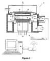
- FIG. 1illustrates one example of a plasma processing system in which sensor probes of the invention may be utilized.
- the plasma processing system 12comprises a vacuum processing chamber 16 , a pumping manifold 18 , a plasma source electrode 20 mounted to the top of the chamber, a gas delivery manifold or gas shroud 22 , gas flow and power connections 24 to the plasma source electrode 20 , a wafer chuck 26 with clamp ring 28 or provision for electrostatic clamping, RF power, fluid coolant, lifting pin, and helium backside-cooling services to the chuck 30 , and a load lock transfer stage with mechanical robotics 32 to manipulate wafers into the chamber 16 and onto the chuck 26 .
- a diagnostic probe 100is comprised of a silicon wafer substrate that incorporates plasma sensor diagnostic circuitry, wireless communications and a stored power system.
- the sensorsare fabricated onto a semiconductor wafer such as a 200 mm or 300 mm diameter silicon wafer.
- the sensorsmay be fabricated onto any process work piece such as a ceramic, plastic, metal or glass work piece surface that can be introduced into the vacuum chamber.
- the probesare fabricated such that normal wafer transfer mechanics and robotics are utilized to move the probe wafers into and out of the plasma processing environment.
- Plasma 34is ignited to perform an etching, stripping, or deposition process on the surface of the wafer, at which time the apparatus sensors and microprocessor are activated or triggered to collect data relating to surface or plasma properties in close proximity to the apparatus surface in real time.
- An on-board wireless transceiver system 36is used to communicate data and instructions with a base station transceiver 38 outside the plasma processing system.
- the base station transceiver 38allows for communication of data and instructions between the software of the external computer 40 and the probe 100 in real time. Alternatively, it is possible to have the probe collect information inside the process and then download data once it is removed from the process chamber.
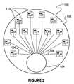
- FIG. 2illustrates a wafer-based plasma probe in accordance with one embodiment of the invention.
- Sensor probe 100comprises a 200 mm or 300 mm silicon wafer primary substrate 102 having physical and electrical properties standard to typical semiconductor starting material. Probe 100 further comprises sensors 110 for measurement of plasma or surface properties.
- An electronics module 104comprising onboard power, communications, and information processing and storage components of probe 100 is disposed upon the surface of probe substrate 102 . Electronics module 104 ay be provided as a prepackaged and sealed unit as described for example in U.S. patent application Ser. No. 10/815,124, owned by the assignee of the present application.
- Conductive interconnections 106are disposed upon substrate 102 for electrical interconnection of sensors 110 to electronics module 104 and electrical components therein.
- a dielectric surface passivation layer(not shown) is disposed upon the wafer surface for physical protection and electrical isolation of conductive interconnections 106 .
- sensors 110are disposed by stepped pattern transfer upon substrate 102 .
- images corresponding to the features of sensor fieldsare contained within sets of photolithographic masks.
- a photomaskis mounted upon an imaging reticle, and the image of the mask is exposed onto a photoresist layer sequentially across the wafer surface using for example a step-and-repeat or step-and-scan projection printing technique.
- the photoresistis developed, leaving resist patterns that define and limit areas affected by subsequent etching, implantation, or other operations performed upon the wafer.
- the image of a succeeding photomask of the mask setis exposed upon a subsequently applied photoresist layer so as to overlay the preceding image, followed by additional feature-building operations upon the wafer.
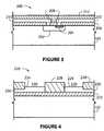
- FIG. 3illustrates an integrated diode temperature sensor disposed by pattern transfer upon substrate 102 according to one embodiment of the invention.
- Diode temperature sensor 200comprises n-type well 202 together with p-type well 204 created within silicon probe substrate 102 .
- Wells 202 and 204may be created using techniques well known in the manufacture of semiconductor devices, as for example by successive application and exposure of photoresist layers through lithographic masks, followed by doping or ion implantation and diffusion to create the desired n-type or p-type regions.
- n-type well 202occupies an area of approximately 10 ⁇ m by 10 ⁇ m
- p-type well 204embedded within n-type well 202
- a dielectric layer 206is disposed upon substrate 102 with contact holes 208 created by further photolithographic and contact etch operations.
- a surface passivation layer 212comprised for example of a dielectric metal oxide, nitride, or oxynitride, is provided for physical protection and electrical isolation of electrical interconnections from the plasma environment.
- two unique scaled currents I 1 and I 2 from the probe controllersequentially bias the temperature diode.
- the two resulting forward diode voltagesare measured and subtracted by the controller to create a difference voltage ⁇ V f .
- a diode current ratio of 10:1results in a difference voltage of 59.6 mV when the diode is at 27° C.
- Other diode current ratioscan be selected in order to increase the measured difference voltage at the temperature diode such as might be necessary to optimize the resolution of a measured wafer temperature, as well as to reduce signal-to-noise in the related A/D measurement circuitry.
- FIG. 4illustrates a dual floating Langmuir probe (DFP) plasma sensor disposed by pattern transfer upon substrate 102 in accordance with another embodiment of the invention.
- DFP sensor 220comprises conductive pads 224 interconnected to remote biasing and measurement circuitry.
- a dielectric layer 222 disposed upon silicon substrate 102insulates conductive pads 224 from the substrate.
- Aluminumis blanket deposited and pattern etched to form conductive pads 224 and electrical interconnection leads 226
- Surface passivation 228is applied, with recesses 230 created through masking and etching operations in order to expose conductive pads 224 to the plasma environment for measurement of ion current flux and apparent electron temperature of the plasma.
- recesses created in an outer passivation layerare filled with plugs of corrosion resistant conductive materials.
- the aluminum conductive pads of a sensorare quickly eroded by the application chemistries, as for example in metal or polysilicon etch operations using chlorine, bromine boron tri-chloride, or other corrosive gases.
- a variety of metalsincluding tungsten, palladium, platinum, molybdenum, and nickel, have significantly greater resistance to these corrosive chemistries.
- a corrosion resistant metalis deposited over the wafer surface.
- the wafer surfaceis then polished, using for example a chemical-mechanical polishing process, until the metal is removed from the outer insulating passivation layer. Plugs of the desired corrosion resistant metal remain in the recess areas, however, which protect the aluminum sensor pads from the corrosive plasma environment.
- an integrated sensor fieldcombines a diode temperature sensor, a DFP sensor, and an electrostatic charge sensor within the field.
- the integrated sensor fieldis replicated across the surface of a wafer diagnostic probe using a step-and-repeat pattern transfer technique. Electrical interconnections are provided between some or all of the sensors of the repeated integrated sensor fields and the electronics and power source of the probe.
- Sensor probes of the inventionmay comprise sensors of any type and number as may be desired to provide spatial and temporal characterization of various plasma or substrate properties, as described for example in U.S. application Ser. Nos. 10/194,526 and 10/640,892.
- Additional plasma or substrate sensorsthat may be disposed by pattern transfer in accordance with the invention include electrostatic charge sensors, optical emission and photo sensors, surface acoustic wave sensors for measuring pressure, film thickness and deposition rates, and the like.
- a diagnostic sensor probe in accordance with the inventionmay include additional sensors disposed by any means.
- FIG. 5illustrates an embodiment of the invention in which electrical interconnections, as well as sensors, are disposed by pattern transfer upon the surface of a diagnostic plasma probe.
- Sensor probe 100comprises sensor fields 110 disposed by stepped pattern transfer upon the probe substrate 102 .
- each of sensor fields 110comprises sensors 120 together with associated electrical interconnection leads 122 for electrical connection of the sensors to an onboard power source and electronics of the wafer probe.
- Sensors 120 of sensor fields 110are of multiple types, including for example both an intergrated temperature diode and a dual floating Langmuir probe. Using step-and-repeat lithography, each of identical sensor fields 110 is patterned onto the surface of substrate 102 .
- sensor fieldsare not identical, but instead comprise different sensor types deployed in a desired configuration across the wafer surface.
- one alternative embodiment of the inventioncomprises a temperature diode sensor field and a complementary DFP sensor field that are patterned alternately across the surface of the wafer probe substrate.
- Fiducial fields 124serve as a a reference or alignment mark during the lithographic operations for transfer of other field patterns to the wafer surface.
- the lithographic transfer of sensor fields of the inventionmay involve many individual process steps, including a sequence of step-and-repeat or step-and-scan exposures with different pattern masks, before the pattern transfer operation is complete.
- electrical interconnection fieldsare also disposed by pattern transfer upon probe substrate 102 .
- Electrical interconnection fieldscomprise conductive pathways for electrical connection of electrical interconnection leads 122 of sensor fields 110 to probe electronics and power source.
- interconnection fieldsmay include horizontal 126 and vertical 128 routing fields, “L” 130 and “T” 132 routing fields, as well as fields providing electrical attachment points 134 corresponding to terminals of an electronics module (not shown).
- a consolidated field 136comprises both sensors 120 and conductive pathways. Electrical interconnection fields are disposed as needed among sensor fields to create a wafer-level electrical interconnection pattern.
- the conductive pathways of interconnection fieldsoverlap and thereby are electrically connected to interconnection leads 122 of sensor fields and/or conductive pathways of other interconnection fields.
- the stitched fields disposed upon the wafer probe surfaceform a wafer-level electrical interconnection pattern that connects sensors of the probe to the probe electronics and power source.
- manufacture of the probe devicemay largely be performed on any modem integrated circuit (IC) production line.
- Manufacturing the probe device in an IC fabrication facilitycan result in significant production efficiencies and cost savings, as well as reduced risks of contamination from equipment or processes not maintained at the cleanliness level dictated by the IC industry.
- the approachalso provides flexibility in that individual pattern modules may be modified or added without the need to remake the entire mask set for the product.
- the patterning of routing and interconnect fieldsmay also be modified to suit the requirements of particular applications or users, improving utility and reducing the costs of customization. “Open” fields, or those having electrical attachment points, provide further flexibility for add-on components, such as remote power modules, third-party sensors, or other electronics.
- FIGS. 6 a and 6 billustrate an alternative embodiment of the invention having sensors and interconnections disposed by hybrid pattern transfer techniques.
- Diagnostic probe 100comprises temperature diode sensor fields 111 disposed across substantially the entire surface of probe substrate 102 by step-and-repeat photolithography.
- Each sensor field 111comprises an integrated temperature diode sensor such as that described in connection with the embodiment illustrated in FIG. 3 , with associated electrical interconnection leads.
- Stepper field masksare created to define the pattern and circuits of sensor fields 111 , and the reticle masks are stepped across the surface of wafer substrate 102 incrementally to place the sensors.
- interconnection field 140is disposed using wafer-level photolithographic pattern transfer operations upon a wafer having temperature diode sensor fields 111 , or other sensor fields, previously disposed thereupon.
- Interconnection field 140comprises conductive pathways 142 for electrical connection of electrical interconnection leads of sensor fields 111 to electronics and power source of probe 100 .
- Alignment marksare provided in interconnection field 140 for alignment of the wafer-level interconnection field mask to the underlying sensor circuits and interconnection leads. Additional alignment marks are also provided in sensor fields 111 to define module-to-module locations and layer-to-layer placement during stepper exposure operations.
- Interconnection field 140further comprises elements of additional sensors for measurement of plasma or substrate properties.
- Interconnection field 140further comprises a plurality of DFP sensor pads 144 and a plurality of differential voltage probe pads 148 .
- Circular DFP sensor pads 144are metallic disks approximately 1.5 mm in diameter.
- Common DFP pad 146serves as a collection pad for each of DFP pads 144 , such that each of DFP pads 144 and common pad 146 operates as a DPF sensor that senses electrical properties of the plasma as between each of DFP pads 144 and common pad 146 .
- Metallic DFP pads 144are disposed so as to shield underlying temperature sensor diodes from ultraviolet radiation emitted from the plasma that would otherwise degrade performance of the diodes.
- Charge sensors 148 for measurement of electrostatic field patterns across the wafer surfaceare disposed as metallic pads adjacent to DFP pads 144 .
- a sensor ground referenceis provided as a ground bus (not shown) routed about the edge of interconnection field 140 .
- an interconnection fieldmay be designed and disposed in a separate lithographic process that selectively interconnects any or virtually all of the sensors to the electronics and power source of the probe device.
- the overlayed interconnection fieldcomprises common power, ground bus, and control lines to which any or all of the previously patterned sensors may be interconnected.
- the wafer probe architecture and functionalitymay thus be tailored to different processes, tools, and user preferences, providing adaptibility and flexibility.
- the interconnection pattern of the probemay be updated without having to modify the entire sensor mask set.
- sensor fieldsmay be improved or updated while retaining the same wafer-level interconnection pattern.
- FIG. 7illustrates a wafer-based diagnostic probe having sensors and photovoltaic power elements disposed by pattern transfer techniques in accordance with another embodiment of the invention.
- Diagnostic probe 100comprises sensor fields 110 disposed by stepped pattern transfer techniques and interconnections 125 as exemplified in embodiments of the invention heretofore described.
- Diagnostic probe 100further comprises photovoltaic power fields 160 , 162 patterned by step-and-repeat lithography processes upon the surface of the probe substrate.
- Each of photovoltaic power fields 160 and 162comprise at least one photovoltaic cell that collects and distributes photovoltaic energy to sensors and electronic subsystems of probe 100
- An exemplary photovoltaic cellcomprises a shallow p-n junction formed using standard IC manufacturing techniques upon the surface of wafer probe 100 , and which converts incident photons to photoelectric power.
- a basic discussion of the physics and operation of photovoltaic devicesappears in Sze, Physics of Semiconductor Devices, pp. 790-838 (1981).
- a photo-transparent protective overcoat(not shown), such as SiO 2 or a polyimide resist material, is disposed to protect the photovoltaic cells from the plasma environment.
- a DC-DC regulator with associated current switching electronicsis provided adjacent to each photoelectric cell for filtering and regulation of power generated by photocells to voltage and current levels required by probe sensors and electronics. Photoelectric cells are optimized for power conversion of either ambient lighting or photo emission from the plasma.
- energy conversion efficiency of a photoelectric cellmay be optimized for a given spectral irradiance by engineering the device band-gap characteristics of the device or by incorporating a multi-layer, thin-film anti-reflection coating which improves transmission of various spectra to the active junction of the photoelectric cell(s).
- photocell of power field 160is optimized for collection of photoelectric energy from typical ambient industrial lighting. In this way, energy collected while the probe is stored in ambient light conditions may be used to recharge a battery or other onboard energy reservoir of the probe.
- Photocell of power field 162optimized to the spectral irradiance generated by plasmas normally imposed upon the wafer probe. When the probe is deployed into a plasma processing environment, energy collected from the photocell of field 162 draws upon the photo emission of the plasma to supplement the power demands of the sensors and electronics of the probe during their operation.
- photovoltaic power fieldsare disposed upon the wafer surface as groups or arrays of photoelectric power cell dies using step-and-repeat lithographic techniques, with the number and size of photocells chosen to provide a desired voltage or power output.
- photovoltaic cellsare disposed upon the surface of discrete elements bonded to the wafer surface, such as upon the probe electronics module. Power derived from photovoltaic cells is provided to central electronics or a distributed power bus for the purpose of powering wholly or in part the probe device.
- photovoltaic cells distributed about a wafer probeprovide power locally to sensors, or groups or clusters of sensors that have been spatially patterned across the wafer.
- FIG. 8illustrates a wafer-based diagnostic probe comprising photovoltaic power fields 162 disposed by stepped pattern transfer. Photocells of photovoltaic power fields 162 are optimized for collection of photoelectric energy from the photo emission of the plasma in the processing environment. Adjacent to each photovoltaic power field 162 are one or more sensor fields 110 disposed by stepped pattern transfer techniques.
- Photovoltaic power and sensor fieldsare field stitched so as to join conductive interconnection pathways of the fields and thereby electrically connect sensors and other elements of sensor fields 110 to the power generating and storage elements of photovoltaic power fields 162 .
- Interconnection between sensors and probe electronics module 104is provided by field-stitched interconnection fields 125 , or alternatively by an overlaid wafer-level interconnection field.
- supplemental photovoltaic fields 160are also provided having photocells optimized for conversion of ambient illumination and interconnected to a power reservoir located within probe electronics module 104 for recharging of the power reservoir during storage periods.
- a diagnostic probecomprises integrated sensor system fields 170 disposed by stepped pattern transfer upon the surface of the probe substrate.
- Integrated system fields 170comprise one or more sensor fields 164 having sensor circuitry for measuring properties of the plasma processing environment.
- Integrated system fields 170further comprise sensor electronics fields 166 interconnected to sensor fields 164 .
- Sensor electronics fields 166comprise analog-to-digital (A/D) circuitry for converting analog electrical signals generated by sensors of sensor fields 164 to digital form.
- Sensor electronics fields 166further comprise digital-to-analog (D/A) circuitry for converting command or control signals sent to the sensors of sensor fields 164 to analog forms required by the sensors.
- sensor fields 164comprise more than one sensor
- a multiplexer circuitis also provided in sensor electronics fields 166 for serial sampling of data from the multiple sensors.
- the signalscan be made more immune to RF noise generated by the plasma environment, thus reducing the number and size of passive RF filtering elements required. Because the A/D and D/A conversions occur in parallel at each sensor, rather than in sequence by a central electronics device, sampling and processing times of sensor data are also improved.
- integrated system field 170also comprises microprocessor 168 , EPROM and RAM memory fields 173 and 174 , wireless communication field 176 with antenna 178 , and power field 172 .
- Microprocessor 168controls the operations of the subsystems of system field 170 , including sampling of data from sensors of sensor field 164 and storage of data in RAM field 174 .
- EPROM field 173contains configuration information about the sensor system and/or wafer probe device, as well as instruction sets and/or program commands for microprocessor 168 .
- Wireless communication field 176together with antenna 178 , transmits and receives communications between the wafer-based sensor system and an external transceiver, and may for example be adapted from single-chip wireless system technologies utilized in mobile communication devices and distributed sensing applications.
- Power field 172comprises photovoltaic power cells with associated power regulation electronics as exemplified in embodiments of the invention heretofore described.
- power fieldscomprise topographically dependent charging devices or other power conversion devices or circuitry disposed by pattern transfer techniques. Interconnections (not shown) among fields are provided as needed, including a common ground connection or conductive plane, as well as local bus connections of power fields to sensors and electronics of the probe device.
- Integrated system fields 170function as Application Specific Integrated Circuit (ASIC) devices that perform high level sensing, computing, data storage, logic, and power management functions, reducing or eliminating need for these electronics in a centralized electronics module or elsewhere on the wafer.
- ASICApplication Specific Integrated Circuit
- each of integrated system fields 170 patterned across the waferdefines a self-contained sensor system capable of performing most or all such functions locally.
- portions of the wafer probe functionality, such as computing, power, or communication functionsmay be managed centrally. Bonding pads 178 are thus provided for wafer-level interconnection of subsystems of system fields 170 to centralized components of these embodiments.
- sensor system fieldsare compartmentalized into separate sensor, power, logic, and communication fields that are interconnected to form complete system fields.
- sensor system fields 180each comprise subfields including sensor and sensor electronics fields 182 , power field 184 , microprocessor field 186 , memory field 188 , and communication field 190 .
- Subfields of sensor system fields 180are disposed by stepped pattern transfer upon the wafer substrate of a diagnostic probe.
- Subfields of sensor system fields 180are field stitched such that bonding pads 192 join and provide electrical interconnectivity.
- subfieldsare connected by a wafer-level interconnection overlay or other interconnection means.
- subfieldsmay be modified or customized individually without the need to recreate the mask set for the entire system field.
- Perimeter bonding pads 194are provided for interconnection of system fields 180 to other system fields or to wafer-level probe components. Open system fields or subfields having appropriate electrical bonding pads or attachment points may be provided to accommodate additional features such as customized sensors, electronics, or power modules.
- the inventionincludes wafer-based probe devices in which sensor system fields, such as those of the aforementioned embodiment, are interconnected into a wafer-level probe architecture.
- the sensing and wireless communication functions of system fieldsoperate independently as part of a wafer-based local area network (LAN).
- LANlocal area network
- each system field or “die”has the ability to broadcast and receive communications independently.
- Each die on the waferis assigned a unique address or other identifier during initialization of the probe device.
- a base stationeither internal or external to the plasma environment, polls each die and receives transmissions of sensor data measured locally to the die, using for example a standard IEEE 802.11 protocol.
- the individual system fields of the wafer probethus operate as a sensor network to provide spatially resolved measurements of surface and plasma properties across the wafer surface and throughout the plasma environment.
- FIG. 11illustrates one example of a plasma processing system in which diced sensor chips of the invention may be utilized.
- Processing system 214comprises a vacuum processing chamber 216 , a pumping manifold 222 , a plasma source 224 mounted to the top of or in communication with the vacuum chamber 216 , a gas delivery manifold or gas shroud (not shown), gas flow, thermal management and power services 228 connecting to the plasma source and system, and a wafer or workpiece chuck or mounting stage 230 .
- the workpiece chuckmay include a clamping means, RF power, fluid coolant, lifting pin assembly, and helium backside-thermal conduction facilities 232 .
- a load lock transfer stage with mechanical robotics 234manipulates and positions a wafer or workpiece 236 .
- Arrays 212 of diagnostic sensors 211are capable of making real-time measurements of plasma properties about the internal boundaries of a plasma processing system 214 . In this particular illustration, two sensor arrays 212 are shown, with one array disposed along the chamber liner 218 , and a second array disposed along the dielectric isolation ring 220 . Alternatively, sensor arrays may be disposed along a focus ring about the wafer mounting stage 230 . Sensors of the apparatus may be used with or without the wafer or workpiece actually present within the processing chamber 216 .
- the outputs 238 and 240 of the sensor arraysare connected to an external electronic subsystem 242 that houses the stimulating electronics, multiplexer, data acquisition and microprocessor controls for the apparatus.
- the output 244 of the electronic subsystem 242is then communicated to a central processor or computer 246 . Since the sensor apparatus can be operated during an actual process, the central processor or computer 246 can use the data from the apparatus to monitoring the process conditions and to provide real-time feedback and control signals to various inputs to the plasma processing system.
- the electronic subsystem 242may be a separate box, a special micro-electronics add-in card associated with another piece of electronic hardware or computer 248 .
- a measurement probecomprises sensor system fields 180 disposed by stepped pattern transfer upon the surface of wafer substrate 102 .
- Sensor system fields 180comprise subfields including, but not limited to, sensor and sensor electronics fields, power fields, microprocessor fields, memory fields, and communication fields.
- Wafer substrate 102is diced into sensor system chips 198 , each sensor system chip 198 comprising a sensor system field 180 .
- Sensor system chips 198are disposed as elements 211 of arrays 212 of diagnostic sensors about internal boundaries of a plasma processing system 214 illustrated in FIG. 11 .
- Sensor elements 211may comprise bonding pads, such as those shown in FIG. 10 , for connection of the chips to power, communication, or other diagnostic or control elements of plasma processing system 214 .
- sensor elements 211are removably affixed to attachment points or receptacles disposed about the processing system so as to be detachable for servicing or replacement.
- Diagnostic sensor arrays 212further comprises an electronics module 213 having communications, power, and processing and control circuitry interconnected to sensor elements 211 .
- Electronics module 213also comprises a wireless communication interface and processing electronics disposed to operate as a base station for polling and receiving sensor data from a wafer-based diagnostic probe.
- Undiced wafer-based diagnostic probe 236configured as a wireless sensor LAN, is introduced into the plasma processing environment as illustrated in FIG. 11 , and the sensors, processing, and communication electronics of the probe are activated to collect and transmit data relating to surface or plasma properties to the electronics module 213 base station.
- the wireless communication interface of electronics module 213also communicates wirelessly with electronic subsystem 242 located outside plasma processing system 214 .
- electronics module 213interrogates and receives data from wafer-based diagnostic probe 236 , then repackages and retransmits the data along with data received from fixed sensor elements 211 to subsystem 242 and computer 246 .
- Electronics module 213further comprises computational circuitry capable of calibrating sensor elements 211 based upon data received from diagnostic probe 236 .
Landscapes
- Chemical & Material Sciences (AREA)
- Engineering & Computer Science (AREA)
- Materials Engineering (AREA)
- Mechanical Engineering (AREA)
- Metallurgy (AREA)
- Organic Chemistry (AREA)
- Physics & Mathematics (AREA)
- Plasma & Fusion (AREA)
- Analytical Chemistry (AREA)
- Drying Of Semiconductors (AREA)
- Plasma Technology (AREA)
- Testing Or Measuring Of Semiconductors Or The Like (AREA)
Abstract
Description
- 1. Field of the Invention
- This invention relates generally to the field of plasma processing, and more particularly to devices for in-situ measurement of plasma properties within a plasma processing system.
- 2. Brief Description of the Prior Art
- With recent developments in the technology of in-situ plasma metrology, it has become possible to obtain virtually noninvasive measurements of actual physical and electrical properties of a plasma within an operational plasma processing environment. For example, a wireless diagnostic plasma probe may comprise sensor devices disposed upon a substrate body that is comparable in physical structure and dimensions to a standard process workpiece, as for example a semiconductor wafer. An onboard power source may be provided, as well as electronic components for collecting, processing and storing data received from the sensors. A wireless communication interface receives and transmits the sensor data outside of the plasma processing environment for further processing and analysis. Further description of the operation and utility of exemplary plasma wafer probe devices is presented in U.S. Patent Application No.10/194,526, assigned to the assignee of the present application.
- Diagnostic plasma sensors may also be disposed at fixed locations within a plasma processing system itself. For example, plasma sensor devices may be disposed along a portion of the chamber liner of a vacuum processing system, about the dielectric isolation ring or gas injection ring of the chamber, or upon a portion of a substrate holder or “chuck.” In-situ sensor arrays may obtain diagnostic data, such as ion current flux and effective electron temperature, from multiple locations about the boundary of the plasma body for use in deducing the global or spatial properties of the plasma. Further description of the operation and utility of exemplary in-situ plasma sensor arrays is presented in U.S. patent application Ser. No. 10/640,892, owned by the assignee of the present application.
- Sensors disposed upon a diagnostic plasma probe may include devices that measure thermal, optical, and electromagnetic properties of the process environment, and ideally include sensors such as dual floating Langmuir probes that can measure physical and electrical properties of the plasma itself without disturbing the properties being measured. In a typical diagnostic probe, sensors may be modular sub-components mounted onto a discrete circuit substrate such as a ceramic or high temperature thermal plastic. Sensor modules are then bonded to the surface of the wafer probe using, for example, a stress relieving adhesive. Alternatively, sensors may be fashioned as diced chips and bonded to the base wafer using flip-chip bonding techniques. U.S. Pat. No. 5,444,637 describes a programmable semiconductor wafer having sensors formed lithographically upon the wafer substrate.
- Output leads of sensors may be connected by wirebond or similar technique to conductive interconnection paths between the sensors and the onboard processing electronics and power source of the wafer probe. Electrical interconnection paths may be formed using silver paint or a silk-screened conductive paste, for example, or alternatively by patterning techniques used in the manufacture of integrated circuits. Materials used in the construction of sensors and sensor modules, as well as those used for adhering and electrically bonding sensors to the probe surface, must all be compatible with and tolerant of the processing environment such that the use of the plasma probe does not result in either physical or chemical contamination of the processing chamber, or of material subsequently processed in the processing chamber.
- For diagnostic plasma measurement probes to be cost effective for high-volume commercial applications, such as in the manufacture of semiconductor devices, it should be possible to mass produce probes for use in large quantities as consumable articles. To this end, a diagnostic probe having a simplified and standardized design with minimal part count would be advantageous. It would be further desireable to utilize manufacturing techniques having reduced risks of product contamination. It would be further desirable to provide enhanced flexibility in customizing or modifying the elements and interconnections of a diagnostic probe for differing applications.
- This invention provides a diagnostic plasma measurement device having sensors and features disposed using pattern transfer fabrication techniques. A measurement device of the invention generally comprises a primary substrate with sensors for measuring plasma or surface properties disposed by stepped pattern transfer about the surface of the probe. Electrical interconnections are provided between the sensors and power, communications, and processing and control elements of the measurement device.
- In one embodiment of the invention, a diagnostic plasma probe comprises a plurality of sensor fields patterned upon a silicon wafer substrate using step-and-repeat photolithography. Sensor fields include sensors that measure physical and electrical properties of a plasma, as well as sensors that measure properties of the wafer surface. In a preferred embodiment, multiple sensor types are combined into a single field that is patterned repeatedly across the wafer surface. The wafer-based probe is introduced into a plasma processing environment and the sensors and processing electronics of the probe are activated to collect data relating to surface or plasma properties. The probe is fitted with an on-board wireless transceiver system for communication of data and instructions with a base station transceiver outside the plasma processing system.
- Embodiments of the invention include integrated diode temperature sensors disposed by pattern transfer upon a substrate of a diagnostic plasma probe device. Embodiments of the invention also include plasma property sensors such as dual floating Langmuir probes disposed by pattern transfer for measurement of ion current flux and apparent electron temperature of the plasma. Additional plasma or substrate sensors disposed by pattern transfer in accordance with the invention include electrostatic charge sensors, optical emission and photo sensors, surface acoustic wave sensors for measuring pressure, film thickness and deposition rates, and the like. In certain embodiments of the invention, sensor pads are protected from the corrosive plasma environment with plugs of corrosion resistant conductive materials applied using for example a damascene process.
- The invention also features electrical interconnections disposed by pattern transfer techniques. In one embodiment of the invention, electrical interconnection fields in addition to sensor fields are disposed by pattern transfer upon the substrate of a wafer-based plasma probe. Electrical interconnection fields comprise conductive pathways for electrical connection of sensor fields to probe electronics and power source. By employing field stitching techniques in the lithographic processes used to create the sensor and interconnection fields, the conductive pathways overlap and electrically connect to interconnection leads of the sensor fields, or to the conductive pathways of other interconnection fields. By creating electrical interconnections as well as sensors of a plasma probe device by pattern transfer techniques, manufacture of the probe device may largely be performed on any modern integrated circuit (IC) production line, and may be modified to suit the requirements of particular applications or users.
- In another embodiment, electrical interconnections on a diagnostic probe device are provided by an overlayed wafer-level interconnection field. In one example, the interconnection field is disposed using wafer-level pattern transfer operations upon a wafer having sensor fields previously disposed by step-and-repeat photolithography. The interconnection field comprises conductive pathways for electrical connection of interconnection leads of the sensor fields to electronics and power source of the probe. In a preferred embodiment, the wafer-level lithographic operations also provide elements of additional plasma or surface sensors. In this approach, the advantages of mass production of die in a traditional IC manufacturing environment are combined with the simplicity and selectivity of wafer-scale pattern transfer techniques.
- Further embodiments of the invention comprise photovoltaic power elements disposed by pattern transfer techniques. The photovoltaic power elements collect and convert radiant energy to electrical energy for use by sensors and electronics of a diagnostic probe device. Photovoltaic elements may be optimized for conversion of ambient light for recharging an onboard energy reservoir of the probe, or of plasma radiance for supplementing the power demands of the sensors and electronics of the probe during their operation. Use of photovoltaic power fields can lessen reliance upon a modular power source such as a battery adhered onto the substrate surface. As a result, the height, weight, and center of mass of an in-situ plasma probe can be better optimized for compatibility with multiple plasma processing platforms.
- In accordance with further embodiments of the invention, logic, processing, communications, and other electronic components and circuitry of a plasma probe device are disposed by pattern transfer techniques. By patterning electronics of the probe in proximity to sensor fields, noise and power loss in the circuits may be substantially reduced. Disposition of these additional features by pattern transfer operations also improves flexibility and reliability of the design while further reducing part counts, size and cost.
- The invention includes wafer-based probe devices in which integrated sensing, processing, and wireless communication fields operate as parts of a wafer-based local area network (LAN). In other embodiments, sensor system fields disposed upon a wafer substrate are diced into sensor chips for fixed placement within a plasma processing system. In this way, for example, sensor and circuit designs may be used for both wafer-based as well as fixed, in-situ diagnostic probes while reducing die cost through economies of scale.
- By utilizing semiconductor fabrications techniques, the invention generally provides reduced risk of contamination by residues of manufacturing steps not maintained at cleanliness level dictated by the IC industry. Use of stepped pattern transfer techniques serves also to reduce part count, simplify fabrication and increase function and reliability of the completed sensor device. A sensor probe design may thus be optimized for cost effective production techniques while ensuring mechanical, chemical, and thermal compatibility with the wafer or other carrying substrate and the environment to which it is exposed.
- Diagnostic probes of the invention are ideally suited for measuring in-situ plasma properties in semiconductor fabrication processes. Devices and technology of the invention are also suitable for use in other plasma applications and process environments. For example, embodiments may be employed in the production of flat panel displays, architectural glass, storage media, and the like. Substrates comprising technology of the invention may include but are not limited to all semiconductor substrates (silicon, gallium arsenide, germanium or others), as well as micro machine substrates, quartz, Pyrex and polymeric substrates.
FIG. 1 illustrates an example of a plasma processing system in which sensor probes of the invention may be utilized.FIG. 2 illustrates a wafer-based plasma probe comprising sensors and other features disposed in accordance with one embodiment of the invention.FIG. 3 illustrates an integrated temperature diode sensor in accordance with one embodiment of the invention.FIG. 4 illustrates dual floating Langmuir probe sensor in accordance with one embodiment of the invention.FIG. 5 illustrates a wafer-based plasma probe comprising sensors, interconnections, and other features disposed in accordance with one embodiment of the invention.FIGS. 6 aand6billustrate a wafer-based plasma probe comprising sensors, interconnections, and other features disposed in accordance with another embodiment of the invention.FIG. 7 illustrates a wafer-based plasma probe comprising sensors, photovoltaic power cells, and other features disposed in accordance with one embodiment of the invention.FIG. 8 illustrates a wafer-based plasma probe comprising sensors, photovoltaic power cells, and other features disposed in accordance with another embodiment of the invention.FIG. 9 illustrates a wafer-based plasma probe comprising sensor system fields and other features disposed in accordance with one embodiment of the invention.FIG. 10 illustrates a wafer-based plasma probe comprising sensor system fields and other features disposed in accordance with another embodiment of the invention.FIG. 11 illustrates a further example of a plasma processing system in which sensor probes of the invention may be utilized.FIG. 12 illustrates the use of sensor system chips in a sensor array in accordance with an embodiment of the invention.FIG. 1 illustrates one example of a plasma processing system in which sensor probes of the invention may be utilized. Theplasma processing system 12 comprises avacuum processing chamber 16, a pumpingmanifold 18, aplasma source electrode 20 mounted to the top of the chamber, a gas delivery manifold orgas shroud 22, gas flow andpower connections 24 to theplasma source electrode 20, awafer chuck 26 withclamp ring 28 or provision for electrostatic clamping, RF power, fluid coolant, lifting pin, and helium backside-cooling services to thechuck 30, and a load lock transfer stage withmechanical robotics 32 to manipulate wafers into thechamber 16 and onto thechuck 26. Adiagnostic probe 100 is comprised of a silicon wafer substrate that incorporates plasma sensor diagnostic circuitry, wireless communications and a stored power system. Preferably, the sensors are fabricated onto a semiconductor wafer such as a 200 mm or 300 mm diameter silicon wafer. Alternatively, the sensors may be fabricated onto any process work piece such as a ceramic, plastic, metal or glass work piece surface that can be introduced into the vacuum chamber. The probes are fabricated such that normal wafer transfer mechanics and robotics are utilized to move the probe wafers into and out of the plasma processing environment.Plasma 34 is ignited to perform an etching, stripping, or deposition process on the surface of the wafer, at which time the apparatus sensors and microprocessor are activated or triggered to collect data relating to surface or plasma properties in close proximity to the apparatus surface in real time. An on-boardwireless transceiver system 36 is used to communicate data and instructions with abase station transceiver 38 outside the plasma processing system. Thebase station transceiver 38 allows for communication of data and instructions between the software of theexternal computer 40 and theprobe 100 in real time. Alternatively, it is possible to have the probe collect information inside the process and then download data once it is removed from the process chamber.FIG. 2 illustrates a wafer-based plasma probe in accordance with one embodiment of the invention.Sensor probe 100 comprises a 200 mm or 300 mm silicon waferprimary substrate 102 having physical and electrical properties standard to typical semiconductor starting material. Probe100 further comprisessensors 110 for measurement of plasma or surface properties. Anelectronics module 104 comprising onboard power, communications, and information processing and storage components ofprobe 100 is disposed upon the surface ofprobe substrate 102.Electronics module 104 ay be provided as a prepackaged and sealed unit as described for example in U.S. patent application Ser. No. 10/815,124, owned by the assignee of the present application.Conductive interconnections 106 are disposed uponsubstrate 102 for electrical interconnection ofsensors 110 toelectronics module 104 and electrical components therein. A dielectric surface passivation layer (not shown) is disposed upon the wafer surface for physical protection and electrical isolation ofconductive interconnections 106.- In accordance with the present invention,
sensors 110 are disposed by stepped pattern transfer uponsubstrate 102. In one approach, images corresponding to the features of sensor fields are contained within sets of photolithographic masks. A photomask is mounted upon an imaging reticle, and the image of the mask is exposed onto a photoresist layer sequentially across the wafer surface using for example a step-and-repeat or step-and-scan projection printing technique. The photoresist is developed, leaving resist patterns that define and limit areas affected by subsequent etching, implantation, or other operations performed upon the wafer. The image of a succeeding photomask of the mask set is exposed upon a subsequently applied photoresist layer so as to overlay the preceding image, followed by additional feature-building operations upon the wafer. This sequential layering process continues until the fabrication of all features of the sensor fields is complete. While use of a photolithographic technique is described in connection with the present embodiment, other techniques such as soft lithography, ink jet lithography, or other forms of “direct write” lithography may be employed for pattern transfer of sensors and features of the invention. FIG. 3 illustrates an integrated diode temperature sensor disposed by pattern transfer uponsubstrate 102 according to one embodiment of the invention.Diode temperature sensor 200 comprises n-type well202 together with p-type well204 created withinsilicon probe substrate 102.Wells type well 202 occupies an area of approximately 10 μm by 10 μm, while p-type well 204, embedded within n-type well 202, occupies an area of approximately 5 μm by 8 μm. Adielectric layer 206 is disposed uponsubstrate 102 withcontact holes 208 created by further photolithographic and contact etch operations. A conductor, such as aluminum, is blanket deposited and etched to form electrical interconnection leads210 in contact with n-type well 202 and p-type well 204. Asurface passivation layer 212, comprised for example of a dielectric metal oxide, nitride, or oxynitride, is provided for physical protection and electrical isolation of electrical interconnections from the plasma environment.- To obtain a temperature measurement, two unique scaled currents I1and I2from the probe controller sequentially bias the temperature diode. The two resulting forward diode voltages are measured and subtracted by the controller to create a difference voltage ΔVf. The difference voltage represents an accurate, process independent relationship to absolute wafer temperature T according to the relationship:
T=ΔVf* q/[k*ln(I2/I1)]
where q is electron charge and k is the Boltzmann constant. Calibration of the bias current ratio at the controller is required to insure the accuracy of the overall temperature sense function. In a preferred embodiment of the invention, a diode current ratio of 10:1 (for example, I1=5 μA and I2=50 μA) results in a difference voltage of 59.6 mV when the diode is at 27° C. Other diode current ratios can be selected in order to increase the measured difference voltage at the temperature diode such as might be necessary to optimize the resolution of a measured wafer temperature, as well as to reduce signal-to-noise in the related A/D measurement circuitry. FIG. 4 illustrates a dual floating Langmuir probe (DFP) plasma sensor disposed by pattern transfer uponsubstrate 102 in accordance with another embodiment of the invention. The operation of DFP sensors generally is described for example in U.S. patent application Ser. No. 10/194,526.DFP sensor 220 comprisesconductive pads 224 interconnected to remote biasing and measurement circuitry. Adielectric layer 222 disposed uponsilicon substrate 102 insulatesconductive pads 224 from the substrate. Aluminum is blanket deposited and pattern etched to formconductive pads 224 and electrical interconnection leads226Surface passivation 228 is applied, withrecesses 230 created through masking and etching operations in order to exposeconductive pads 224 to the plasma environment for measurement of ion current flux and apparent electron temperature of the plasma.- In alternative embodiments of the invention, recesses created in an outer passivation layer, such as those depicted in the foregoing embodiment, are filled with plugs of corrosion resistant conductive materials. For some processing applications, the aluminum conductive pads of a sensor are quickly eroded by the application chemistries, as for example in metal or polysilicon etch operations using chlorine, bromine boron tri-chloride, or other corrosive gases. A variety of metals, including tungsten, palladium, platinum, molybdenum, and nickel, have significantly greater resistance to these corrosive chemistries. After forming a recess to expose a sensor pad, such as the
recesses 230 shown inFIG. 4 , a corrosion resistant metal is deposited over the wafer surface. The wafer surface is then polished, using for example a chemical-mechanical polishing process, until the metal is removed from the outer insulating passivation layer. Plugs of the desired corrosion resistant metal remain in the recess areas, however, which protect the aluminum sensor pads from the corrosive plasma environment. - In a preferred embodiment of the invention, an integrated sensor field combines a diode temperature sensor, a DFP sensor, and an electrostatic charge sensor within the field. The integrated sensor field is replicated across the surface of a wafer diagnostic probe using a step-and-repeat pattern transfer technique. Electrical interconnections are provided between some or all of the sensors of the repeated integrated sensor fields and the electronics and power source of the probe.
- Sensor probes of the invention may comprise sensors of any type and number as may be desired to provide spatial and temporal characterization of various plasma or substrate properties, as described for example in U.S. application Ser. Nos. 10/194,526 and 10/640,892. Additional plasma or substrate sensors that may be disposed by pattern transfer in accordance with the invention include electrostatic charge sensors, optical emission and photo sensors, surface acoustic wave sensors for measuring pressure, film thickness and deposition rates, and the like. A diagnostic sensor probe in accordance with the invention may include additional sensors disposed by any means.
FIG. 5 illustrates an embodiment of the invention in which electrical interconnections, as well as sensors, are disposed by pattern transfer upon the surface of a diagnostic plasma probe.Sensor probe 100 comprisessensor fields 110 disposed by stepped pattern transfer upon theprobe substrate 102. In this embodiment, each ofsensor fields 110 comprisessensors 120 together with associated electrical interconnection leads122 for electrical connection of the sensors to an onboard power source and electronics of the wafer probe.Sensors 120 ofsensor fields 110 are of multiple types, including for example both an intergrated temperature diode and a dual floating Langmuir probe. Using step-and-repeat lithography, each of identical sensor fields110 is patterned onto the surface ofsubstrate 102. In other embodiments, sensor fields are not identical, but instead comprise different sensor types deployed in a desired configuration across the wafer surface. Thus, for example, one alternative embodiment of the invention comprises a temperature diode sensor field and a complementary DFP sensor field that are patterned alternately across the surface of the wafer probe substrate. Fiducial fields124 serve as a a reference or alignment mark during the lithographic operations for transfer of other field patterns to the wafer surface. As will be readily appreciated, the lithographic transfer of sensor fields of the invention may involve many individual process steps, including a sequence of step-and-repeat or step-and-scan exposures with different pattern masks, before the pattern transfer operation is complete.- Referring again to
FIG. 5 , electrical interconnection fields are also disposed by pattern transfer uponprobe substrate 102. Electrical interconnection fields comprise conductive pathways for electrical connection of electrical interconnection leads122 ofsensor fields 110 to probe electronics and power source. As depicted inFIG. 5 interconnection fields may include horizontal126 and vertical128 routing fields, “L”130 and “T”132 routing fields, as well as fields providing electrical attachment points134 corresponding to terminals of an electronics module (not shown). Aconsolidated field 136 comprises bothsensors 120 and conductive pathways. Electrical interconnection fields are disposed as needed among sensor fields to create a wafer-level electrical interconnection pattern. By employing field stitching techniques in the lithographic processes used to create the sensor and interconnection fields, the conductive pathways of interconnection fields overlap and thereby are electrically connected to interconnection leads122 of sensor fields and/or conductive pathways of other interconnection fields. As a result, the stitched fields disposed upon the wafer probe surface form a wafer-level electrical interconnection pattern that connects sensors of the probe to the probe electronics and power source. - By creating electrical interconnections as well as sensors of a plasma probe device by pattern transfer techniques, manufacture of the probe device may largely be performed on any modem integrated circuit (IC) production line. Manufacturing the probe device in an IC fabrication facility can result in significant production efficiencies and cost savings, as well as reduced risks of contamination from equipment or processes not maintained at the cleanliness level dictated by the IC industry. The approach also provides flexibility in that individual pattern modules may be modified or added without the need to remake the entire mask set for the product. The patterning of routing and interconnect fields may also be modified to suit the requirements of particular applications or users, improving utility and reducing the costs of customization. “Open” fields, or those having electrical attachment points, provide further flexibility for add-on components, such as remote power modules, third-party sensors, or other electronics.
FIGS. 6 aand6billustrate an alternative embodiment of the invention having sensors and interconnections disposed by hybrid pattern transfer techniques.Diagnostic probe 100 comprises temperaturediode sensor fields 111 disposed across substantially the entire surface ofprobe substrate 102 by step-and-repeat photolithography. Eachsensor field 111 comprises an integrated temperature diode sensor such as that described in connection with the embodiment illustrated inFIG. 3 , with associated electrical interconnection leads. Stepper field masks are created to define the pattern and circuits ofsensor fields 111, and the reticle masks are stepped across the surface ofwafer substrate 102 incrementally to place the sensors.- Electrical interconnections are disposed upon
probe substrate 102 by overlayedinterconnection field 140. In a preferred embodiment,interconnection field 140 is disposed using wafer-level photolithographic pattern transfer operations upon a wafer having temperaturediode sensor fields 111, or other sensor fields, previously disposed thereupon.Interconnection field 140 comprisesconductive pathways 142 for electrical connection of electrical interconnection leads ofsensor fields 111 to electronics and power source ofprobe 100. Alignment marks are provided ininterconnection field 140 for alignment of the wafer-level interconnection field mask to the underlying sensor circuits and interconnection leads. Additional alignment marks are also provided insensor fields 111 to define module-to-module locations and layer-to-layer placement during stepper exposure operations. Interconnection field 140 further comprises elements of additional sensors for measurement of plasma or substrate properties.Interconnection field 140 further comprises a plurality ofDFP sensor pads 144 and a plurality of differentialvoltage probe pads 148. CircularDFP sensor pads 144 are metallic disks approximately 1.5 mm in diameter.Common DFP pad 146 serves as a collection pad for each ofDFP pads 144, such that each ofDFP pads 144 andcommon pad 146 operates as a DPF sensor that senses electrical properties of the plasma as between each ofDFP pads 144 andcommon pad 146.Metallic DFP pads 144 are disposed so as to shield underlying temperature sensor diodes from ultraviolet radiation emitted from the plasma that would otherwise degrade performance of the diodes.Charge sensors 148 for measurement of electrostatic field patterns across the wafer surface are disposed as metallic pads adjacent toDFP pads 144. A sensor ground reference is provided as a ground bus (not shown) routed about the edge ofinterconnection field 140.- While retaining the advantages of manufacturing the probe device on modern IC production lines, use of hybrid pattern transfer techniques results in additional advantages. A variety of sensor technologies may be incorporated into a sensor field that is patterned economically in large numbers across substantially the entire surface of a probe substrate. With the sensor fields already thus disposed, an interconnection field may be designed and disposed in a separate lithographic process that selectively interconnects any or virtually all of the sensors to the electronics and power source of the probe device. In certain embodiments of the invention, the overlayed interconnection field comprises common power, ground bus, and control lines to which any or all of the previously patterned sensors may be interconnected. The wafer probe architecture and functionality may thus be tailored to different processes, tools, and user preferences, providing adaptibility and flexibility. To add or remove sensors, the interconnection pattern of the probe may be updated without having to modify the entire sensor mask set. Alternatively, sensor fields may be improved or updated while retaining the same wafer-level interconnection pattern.
FIG. 7 illustrates a wafer-based diagnostic probe having sensors and photovoltaic power elements disposed by pattern transfer techniques in accordance with another embodiment of the invention.Diagnostic probe 100 comprisessensor fields 110 disposed by stepped pattern transfer techniques andinterconnections 125 as exemplified in embodiments of the invention heretofore described.Diagnostic probe 100 further comprises photovoltaic power fields160,162 patterned by step-and-repeat lithography processes upon the surface of the probe substrate. Each of photovoltaic power fields160 and162 comprise at least one photovoltaic cell that collects and distributes photovoltaic energy to sensors and electronic subsystems ofprobe 100- An exemplary photovoltaic cell comprises a shallow p-n junction formed using standard IC manufacturing techniques upon the surface of
wafer probe 100, and which converts incident photons to photoelectric power. A basic discussion of the physics and operation of photovoltaic devices appears in Sze, Physics of Semiconductor Devices, pp. 790-838 (1981). A photo-transparent protective overcoat (not shown), such as SiO2or a polyimide resist material, is disposed to protect the photovoltaic cells from the plasma environment. A DC-DC regulator with associated current switching electronics is provided adjacent to each photoelectric cell for filtering and regulation of power generated by photocells to voltage and current levels required by probe sensors and electronics. Photoelectric cells are optimized for power conversion of either ambient lighting or photo emission from the plasma. By way of example, energy conversion efficiency of a photoelectric cell may be optimized for a given spectral irradiance by engineering the device band-gap characteristics of the device or by incorporating a multi-layer, thin-film anti-reflection coating which improves transmission of various spectra to the active junction of the photoelectric cell(s). Referring toFIG. 7 , photocell of power field160 is optimized for collection of photoelectric energy from typical ambient industrial lighting. In this way, energy collected while the probe is stored in ambient light conditions may be used to recharge a battery or other onboard energy reservoir of the probe. Photocell ofpower field 162 optimized to the spectral irradiance generated by plasmas normally imposed upon the wafer probe. When the probe is deployed into a plasma processing environment, energy collected from the photocell offield 162 draws upon the photo emission of the plasma to supplement the power demands of the sensors and electronics of the probe during their operation. - As illustrated in
FIG. 7 , photovoltaic power fields are disposed upon the wafer surface as groups or arrays of photoelectric power cell dies using step-and-repeat lithographic techniques, with the number and size of photocells chosen to provide a desired voltage or power output. In alternative embodiments, photovoltaic cells are disposed upon the surface of discrete elements bonded to the wafer surface, such as upon the probe electronics module. Power derived from photovoltaic cells is provided to central electronics or a distributed power bus for the purpose of powering wholly or in part the probe device. - In other embodiments of the invention, photovoltaic cells distributed about a wafer probe provide power locally to sensors, or groups or clusters of sensors that have been spatially patterned across the wafer.
FIG. 8 illustrates a wafer-based diagnostic probe comprising photovoltaic power fields162 disposed by stepped pattern transfer. Photocells of photovoltaic power fields162 are optimized for collection of photoelectric energy from the photo emission of the plasma in the processing environment. Adjacent to eachphotovoltaic power field 162 are one ormore sensor fields 110 disposed by stepped pattern transfer techniques. Photovoltaic power and sensor fields are field stitched so as to join conductive interconnection pathways of the fields and thereby electrically connect sensors and other elements ofsensor fields 110 to the power generating and storage elements of photovoltaic power fields162. Interconnection between sensors andprobe electronics module 104 is provided by field-stitchedinterconnection fields 125, or alternatively by an overlaid wafer-level interconnection field. By locating photovoltaic power fields162 in close proximity to power consuming circuits ofsensor fields 110, resistive losses and parasitic reactance associated with tightly pitched conductive lines created by lithographic fabrication are reduced. In preferred embodiments, supplemental photovoltaic fields160 are also provided having photocells optimized for conversion of ambient illumination and interconnected to a power reservoir located withinprobe electronics module 104 for recharging of the power reservoir during storage periods. - A further embodiment of the invention comprising both sensors and probe electronic elements disposed by pattern transfer techniques is illustrated in
FIG. 9 . A diagnostic probe comprises integrated sensor system fields170 disposed by stepped pattern transfer upon the surface of the probe substrate. Integrated system fields170 comprise one ormore sensor fields 164 having sensor circuitry for measuring properties of the plasma processing environment. Integrated system fields170 further comprisesensor electronics fields 166 interconnected to sensor fields164. Sensor electronics fields166 comprise analog-to-digital (A/D) circuitry for converting analog electrical signals generated by sensors ofsensor fields 164 to digital form. Sensor electronics fields166 further comprise digital-to-analog (D/A) circuitry for converting command or control signals sent to the sensors ofsensor fields 164 to analog forms required by the sensors. In the event that sensor fields164 comprise more than one sensor, a multiplexer circuit is also provided insensor electronics fields 166 for serial sampling of data from the multiple sensors. By providing for transmission of signals to and from sensors of the plasma probe in digital form, the signals can be made more immune to RF noise generated by the plasma environment, thus reducing the number and size of passive RF filtering elements required. Because the A/D and D/A conversions occur in parallel at each sensor, rather than in sequence by a central electronics device, sampling and processing times of sensor data are also improved. - As illustrated in
FIG. 9 , integratedsystem field 170 also comprisesmicroprocessor 168, EPROM andRAM memory fields wireless communication field 176 withantenna 178, andpower field 172.Microprocessor 168 controls the operations of the subsystems ofsystem field 170, including sampling of data from sensors ofsensor field 164 and storage of data inRAM field 174.EPROM field 173 contains configuration information about the sensor system and/or wafer probe device, as well as instruction sets and/or program commands formicroprocessor 168.Wireless communication field 176, together withantenna 178, transmits and receives communications between the wafer-based sensor system and an external transceiver, and may for example be adapted from single-chip wireless system technologies utilized in mobile communication devices and distributed sensing applications.Power field 172 comprises photovoltaic power cells with associated power regulation electronics as exemplified in embodiments of the invention heretofore described. Alternatively, power fields comprise topographically dependent charging devices or other power conversion devices or circuitry disposed by pattern transfer techniques. Interconnections (not shown) among fields are provided as needed, including a common ground connection or conductive plane, as well as local bus connections of power fields to sensors and electronics of the probe device. - Integrated system fields170 function as Application Specific Integrated Circuit (ASIC) devices that perform high level sensing, computing, data storage, logic, and power management functions, reducing or eliminating need for these electronics in a centralized electronics module or elsewhere on the wafer. In the embodiment illustrated in
FIG. 9 , each of integrated system fields170 patterned across the wafer defines a self-contained sensor system capable of performing most or all such functions locally. In other embodiments, portions of the wafer probe functionality, such as computing, power, or communication functions, may be managed centrally.Bonding pads 178 are thus provided for wafer-level interconnection of subsystems of system fields170 to centralized components of these embodiments. - In yet other embodiments, sensor system fields are compartmentalized into separate sensor, power, logic, and communication fields that are interconnected to form complete system fields. Referring to
FIG. 10 , sensor system fields180 each comprise subfields including sensor andsensor electronics fields 182,power field 184,microprocessor field 186,memory field 188, andcommunication field 190. Subfields of sensor system fields180 are disposed by stepped pattern transfer upon the wafer substrate of a diagnostic probe. Subfields of sensor system fields180 are field stitched such thatbonding pads 192 join and provide electrical interconnectivity. Alternatively, subfields are connected by a wafer-level interconnection overlay or other interconnection means. In this approach, subfields may be modified or customized individually without the need to recreate the mask set for the entire system field.Perimeter bonding pads 194 are provided for interconnection of system fields180 to other system fields or to wafer-level probe components. Open system fields or subfields having appropriate electrical bonding pads or attachment points may be provided to accommodate additional features such as customized sensors, electronics, or power modules. - The invention includes wafer-based probe devices in which sensor system fields, such as those of the aforementioned embodiment, are interconnected into a wafer-level probe architecture. Alternatively, the sensing and wireless communication functions of system fields operate independently as part of a wafer-based local area network (LAN). In this embodiment, rather than transmitting measurement data through a central communication module, each system field or “die” has the ability to broadcast and receive communications independently. Each die on the wafer is assigned a unique address or other identifier during initialization of the probe device. A base station, either internal or external to the plasma environment, polls each die and receives transmissions of sensor data measured locally to the die, using for example a standard IEEE 802.11 protocol. The individual system fields of the wafer probe thus operate as a sensor network to provide spatially resolved measurements of surface and plasma properties across the wafer surface and throughout the plasma environment.
- In another application of the invention, sensor system fields disposed upon a wafer subsrate are diced into sensor chips for fixed placement within a plasma processing system.
FIG. 11 illustrates one example of a plasma processing system in which diced sensor chips of the invention may be utilized.Processing system 214 comprises avacuum processing chamber 216, apumping manifold 222, aplasma source 224 mounted to the top of or in communication with thevacuum chamber 216, a gas delivery manifold or gas shroud (not shown), gas flow, thermal management andpower services 228 connecting to the plasma source and system, and a wafer or workpiece chuck or mountingstage 230. The workpiece chuck may include a clamping means, RF power, fluid coolant, lifting pin assembly, and helium backside-thermal conduction facilities 232. A load lock transfer stage withmechanical robotics 234 manipulates and positions a wafer orworkpiece 236.Arrays 212 ofdiagnostic sensors 211 are capable of making real-time measurements of plasma properties about the internal boundaries of aplasma processing system 214. In this particular illustration, twosensor arrays 212 are shown, with one array disposed along thechamber liner 218, and a second array disposed along thedielectric isolation ring 220. Alternatively, sensor arrays may be disposed along a focus ring about thewafer mounting stage 230. Sensors of the apparatus may be used with or without the wafer or workpiece actually present within theprocessing chamber 216. - The
outputs electronic subsystem 242 that houses the stimulating electronics, multiplexer, data acquisition and microprocessor controls for the apparatus. Theoutput 244 of theelectronic subsystem 242 is then communicated to a central processor orcomputer 246. Since the sensor apparatus can be operated during an actual process, the central processor orcomputer 246 can use the data from the apparatus to monitoring the process conditions and to provide real-time feedback and control signals to various inputs to the plasma processing system. Theelectronic subsystem 242 may be a separate box, a special micro-electronics add-in card associated with another piece of electronic hardware or computer248. - Referring to
FIG. 12 , a measurement probe comprises sensor system fields180 disposed by stepped pattern transfer upon the surface ofwafer substrate 102. Sensor system fields180 comprise subfields including, but not limited to, sensor and sensor electronics fields, power fields, microprocessor fields, memory fields, and communication fields.Wafer substrate 102 is diced into sensor system chips198, eachsensor system chip 198 comprising asensor system field 180. Sensor system chips198 are disposed aselements 211 ofarrays 212 of diagnostic sensors about internal boundaries of aplasma processing system 214 illustrated inFIG. 11 .Sensor elements 211 may comprise bonding pads, such as those shown inFIG. 10 , for connection of the chips to power, communication, or other diagnostic or control elements ofplasma processing system 214. In preferred embodiments,sensor elements 211 are removably affixed to attachment points or receptacles disposed about the processing system so as to be detachable for servicing or replacement. Diagnostic sensor arrays 212 further comprises anelectronics module 213 having communications, power, and processing and control circuitry interconnected tosensor elements 211.Electronics module 213 also comprises a wireless communication interface and processing electronics disposed to operate as a base station for polling and receiving sensor data from a wafer-based diagnostic probe. Undiced wafer-baseddiagnostic probe 236, configured as a wireless sensor LAN, is introduced into the plasma processing environment as illustrated inFIG. 11 , and the sensors, processing, and communication electronics of the probe are activated to collect and transmit data relating to surface or plasma properties to theelectronics module 213 base station. In a preferred embodiment, the wireless communication interface ofelectronics module 213 also communicates wirelessly withelectronic subsystem 242 located outsideplasma processing system 214. In this embodiment,electronics module 213 interrogates and receives data from wafer-baseddiagnostic probe 236, then repackages and retransmits the data along with data received from fixedsensor elements 211 tosubsystem 242 andcomputer 246.Electronics module 213 further comprises computational circuitry capable of calibratingsensor elements 211 based upon data received fromdiagnostic probe 236.- Although there is illustrated and described herein specific structure and details of operation, it is to be understood that these descriptions are exemplary and that alternative embodiments and equivalents may be readily made by those skilled in the art without departing from the spirit and the scope of this invention. Accordingly, the invention is intended to embrace all such alternatives and equivalents that fall within the spirit and scope of the appended claims.
Claims (34)
Priority Applications (3)
| Application Number | Priority Date | Filing Date | Title |
|---|---|---|---|
| US10/875,954US20050284570A1 (en) | 2004-06-24 | 2004-06-24 | Diagnostic plasma measurement device having patterned sensors and features |
| PCT/US2005/020394WO2006011954A2 (en) | 2004-06-24 | 2005-06-09 | Diagnostic plasma measurement device having patterned sensors and features |
| TW094119794ATW200611295A (en) | 2004-06-24 | 2005-06-15 | Diagnostic plasma measurement device having patterned sensors and features |
Applications Claiming Priority (1)
| Application Number | Priority Date | Filing Date | Title |
|---|---|---|---|
| US10/875,954US20050284570A1 (en) | 2004-06-24 | 2004-06-24 | Diagnostic plasma measurement device having patterned sensors and features |
Publications (1)
| Publication Number | Publication Date |
|---|---|
| US20050284570A1true US20050284570A1 (en) | 2005-12-29 |
Family
ID=35504323
Family Applications (1)
| Application Number | Title | Priority Date | Filing Date |
|---|---|---|---|
| US10/875,954AbandonedUS20050284570A1 (en) | 2004-06-24 | 2004-06-24 | Diagnostic plasma measurement device having patterned sensors and features |
Country Status (3)
| Country | Link |
|---|---|
| US (1) | US20050284570A1 (en) |
| TW (1) | TW200611295A (en) |
| WO (1) | WO2006011954A2 (en) |
Cited By (19)
| Publication number | Priority date | Publication date | Assignee | Title |
|---|---|---|---|---|
| US20060171848A1 (en)* | 2005-01-31 | 2006-08-03 | Advanced Energy Industries, Inc. | Diagnostic plasma sensors for endpoint and end-of-life detection |
| US7153709B1 (en)* | 2004-08-31 | 2006-12-26 | Advanced Micro Devices, Inc. | Method and apparatus for calibrating degradable components using process state data |
| WO2007099499A3 (en)* | 2006-02-28 | 2008-05-08 | Ecole Polytech | Method for deposition of a sensor on a conductive substrate |
| US20090061542A1 (en)* | 2007-09-04 | 2009-03-05 | Lam Research Corporation | Method and apparatus for diagnosing status of parts in real time in plasma processing equipment |
| US20110035043A1 (en)* | 2009-08-07 | 2011-02-10 | Taiwan Semiconductor Manufacturing Company, Ltd. | Method and apparatus for wireless transmission of diagnostic information |
| US7960670B2 (en) | 2005-05-03 | 2011-06-14 | Kla-Tencor Corporation | Methods of and apparatuses for measuring electrical parameters of a plasma process |
| US8104342B2 (en) | 2007-02-23 | 2012-01-31 | Kla-Tencor Corporation | Process condition measuring device |
| WO2015069602A1 (en)* | 2013-11-11 | 2015-05-14 | Applied Materials, Inc. | Smart device fabrication via precision patterning |
| US20160048111A1 (en)* | 2014-08-15 | 2016-02-18 | Applied Materials, Inc. | Method of real time in-situ chamber condition monitoring using sensors and rf communication |
| US20160116518A1 (en)* | 2014-10-28 | 2016-04-28 | Applied Materials, Inc. | Real-time measurement of a surface charge profile of an electrostatic chuck |
| US20170221783A1 (en)* | 2016-01-28 | 2017-08-03 | Leonard TEDESCHI | Self-aware production wafers |
| US20170365531A1 (en)* | 2016-06-20 | 2017-12-21 | Applied Materials, Inc. | Wafer processing equipment having capacitive micro sensors |
| US20180313697A1 (en)* | 2015-10-19 | 2018-11-01 | Novena Tec Inc. | Process monitoring device |
| US10216100B2 (en) | 2015-07-16 | 2019-02-26 | Asml Netherlands B.V. | Inspection substrate and an inspection method |
| US10508896B2 (en) | 2015-11-25 | 2019-12-17 | Asml Netherlands B.V. | Measurement substrate and a measurement method |
| JP2020517112A (en)* | 2017-04-14 | 2020-06-11 | イオニアー エルエルシーIoneer, Llc | Method and system for measuring plasma emission in a plasma processing reactor |
| US20210101249A1 (en)* | 2015-12-10 | 2021-04-08 | Ioneer, LLC. | Apparatus and method for determining parameters of process operation |
| US11901875B2 (en) | 2020-10-12 | 2024-02-13 | Applied Materials, Inc. | Surface acoustic wave sensor assembly |
| US11920994B2 (en) | 2020-10-12 | 2024-03-05 | Applied Materials, Inc. | Surface acoustic wave sensor assembly |
Families Citing this family (2)
| Publication number | Priority date | Publication date | Assignee | Title |
|---|---|---|---|---|
| US12272520B2 (en) | 2019-07-09 | 2025-04-08 | Tokyo Electron Limited | Process control enabled VDC sensor for plasma process |
| US11781214B2 (en) | 2019-07-30 | 2023-10-10 | Applied Materials, Inc. | Differential capacitive sensors for in-situ film thickness and dielectric constant measurement |
Citations (39)
| Publication number | Priority date | Publication date | Assignee | Title |
|---|---|---|---|---|
| US4006404A (en)* | 1976-01-30 | 1977-02-01 | The United States Of America As Represented By The Secretary Of The Navy | Pulsed plasma probe |
| US4577056A (en)* | 1984-04-09 | 1986-03-18 | Olin Corporation | Hermetically sealed metal package |
| US5167748A (en)* | 1990-09-06 | 1992-12-01 | Charles Evans And Associates | Plasma etching method and apparatus |
| US5167640A (en)* | 1991-07-31 | 1992-12-01 | Balding James G | Syringe needle shield |
| US5200640A (en)* | 1991-08-12 | 1993-04-06 | Electron Power Inc. | Hermetic package having covers and a base providing for direct electrical connection |
| US5339039A (en)* | 1992-09-29 | 1994-08-16 | Arizona Board Of Regents On Behalf Of The University Of Arizona | Langmuir probe system for radio frequency excited plasma processing system |
| US5444637A (en)* | 1993-09-28 | 1995-08-22 | Advanced Micro Devices, Inc. | Programmable semiconductor wafer for sensing, recording and retrieving fabrication process conditions to which the wafer is exposed |
| US5451784A (en)* | 1994-10-31 | 1995-09-19 | Applied Materials, Inc. | Composite diagnostic wafer for semiconductor wafer processing systems |
| US5467013A (en)* | 1993-12-07 | 1995-11-14 | Sematech, Inc. | Radio frequency monitor for semiconductor process control |
| US5471115A (en)* | 1993-09-16 | 1995-11-28 | Fujitsu Limited | Method and apparatus for measuring electron density of plasma |
| US5526293A (en)* | 1993-12-17 | 1996-06-11 | Texas Instruments Inc. | System and method for controlling semiconductor wafer processing |
| US5594328A (en)* | 1995-02-14 | 1997-01-14 | Lukaszek; Wieslaw A. | Passive probe employing cluster of charge monitors for determining simultaneous charging characteristics of wafer environment inside IC process equipment |
| US5667701A (en)* | 1995-06-07 | 1997-09-16 | Applied Materials, Inc. | Method of measuring the amount of capacitive coupling of RF power in an inductively coupled plasma |
| US5786548A (en)* | 1996-08-15 | 1998-07-28 | Hughes Electronics Corporation | Hermetic package for an electrical device |
| US5801386A (en)* | 1995-12-11 | 1998-09-01 | Applied Materials, Inc. | Apparatus for measuring plasma characteristics within a semiconductor wafer processing system and a method of fabricating and using same |
| US5885402A (en)* | 1996-07-17 | 1999-03-23 | Applied Materials | Diagnostic head assembly for plasma chamber |
| US5936413A (en)* | 1995-09-19 | 1999-08-10 | Centre National De La Recherche Scientifique | Method and device for measuring an ion flow in a plasma |
| US5959309A (en)* | 1997-04-07 | 1999-09-28 | Industrial Technology Research Institute | Sensor to monitor plasma induced charging damage |
| US5967661A (en)* | 1997-06-02 | 1999-10-19 | Sensarray Corporation | Temperature calibration substrate |
| US5969639A (en)* | 1997-07-28 | 1999-10-19 | Lockheed Martin Energy Research Corporation | Temperature measuring device |
| US5989349A (en)* | 1997-06-24 | 1999-11-23 | Applied Materials, Inc. | Diagnostic pedestal assembly for a semiconductor wafer processing system |
| US6033922A (en)* | 1997-12-19 | 2000-03-07 | Advanced Micro Devices, Inc. | Monitoring wafer temperature during thermal processing of wafers by measuring sheet resistance of a test wafer |
| US6051443A (en)* | 1996-12-16 | 2000-04-18 | Stmicroelectronics S.R.L | Method for assessing the effects of plasma treatments on wafers of semiconductor material |
| US6113733A (en)* | 1996-11-08 | 2000-09-05 | Matsushita Electric Industrial Co., Ltd. | Apparatus and method for optical evaluation, apparatus and method for manufacturing semiconductor device, method of controlling apparatus for manufacturing semiconductor device, and semiconductor device |
| US6190040B1 (en)* | 1999-05-10 | 2001-02-20 | Sensarray Corporation | Apparatus for sensing temperature on a substrate in an integrated circuit fabrication tool |
| US6244121B1 (en)* | 1998-03-06 | 2001-06-12 | Applied Materials, Inc. | Sensor device for non-intrusive diagnosis of a semiconductor processing system |
| US6325536B1 (en)* | 1998-07-10 | 2001-12-04 | Sensarray Corporation | Integrated wafer temperature sensors |
| US6339297B1 (en)* | 1998-07-23 | 2002-01-15 | Nissin Inc. | Plasma density information measuring method, probe used for measuring plasma density information, and plasma density information measuring apparatus |
| US6458239B1 (en)* | 1996-09-27 | 2002-10-01 | Surface Technology Systems Plc | Plasma processing apparatus |
| US20020173059A1 (en)* | 2001-05-18 | 2002-11-21 | Shawming Ma | Method of real-time plasma charging voltage measurement on powered electrode with electrostatic chuck in plasma process chambers |
| US6576922B1 (en)* | 2001-12-21 | 2003-06-10 | Texas Instruments Incorporated | Ferroelectric capacitor plasma charging monitor |
| US20030127589A1 (en)* | 2001-06-28 | 2003-07-10 | Greene, Tweed & Co. | Self contained sensing apparatus and system |
| US6614051B1 (en)* | 2002-05-10 | 2003-09-02 | Applied Materials, Inc. | Device for monitoring substrate charging and method of fabricating same |
| US6616332B1 (en)* | 1999-11-18 | 2003-09-09 | Sensarray Corporation | Optical techniques for measuring parameters such as temperature across a surface |
| US20040007326A1 (en)* | 2002-07-12 | 2004-01-15 | Roche Gregory A. | Wafer probe for measuring plasma and surface characteristics in plasma processing enviroments |
| US6691068B1 (en)* | 2000-08-22 | 2004-02-10 | Onwafer Technologies, Inc. | Methods and apparatus for obtaining data for process operation, optimization, monitoring, and control |
| US20040074323A1 (en)* | 2002-01-24 | 2004-04-22 | Renken Wayne G. | Process condition sensing wafer and data analysis system |
| US6738722B2 (en)* | 2001-04-19 | 2004-05-18 | Onwafer Technologies, Inc. | Data collection and correction methods and apparatus |
| US6771481B2 (en)* | 2000-12-28 | 2004-08-03 | Hitachi, Ltd. | Plasma processing apparatus for processing semiconductor wafer using plasma |
- 2004
- 2004-06-24USUS10/875,954patent/US20050284570A1/ennot_activeAbandoned
- 2005
- 2005-06-09WOPCT/US2005/020394patent/WO2006011954A2/enactiveApplication Filing
- 2005-06-15TWTW094119794Apatent/TW200611295A/enunknown
Patent Citations (39)
| Publication number | Priority date | Publication date | Assignee | Title |
|---|---|---|---|---|
| US4006404A (en)* | 1976-01-30 | 1977-02-01 | The United States Of America As Represented By The Secretary Of The Navy | Pulsed plasma probe |
| US4577056A (en)* | 1984-04-09 | 1986-03-18 | Olin Corporation | Hermetically sealed metal package |
| US5167748A (en)* | 1990-09-06 | 1992-12-01 | Charles Evans And Associates | Plasma etching method and apparatus |
| US5167640A (en)* | 1991-07-31 | 1992-12-01 | Balding James G | Syringe needle shield |
| US5200640A (en)* | 1991-08-12 | 1993-04-06 | Electron Power Inc. | Hermetic package having covers and a base providing for direct electrical connection |
| US5339039A (en)* | 1992-09-29 | 1994-08-16 | Arizona Board Of Regents On Behalf Of The University Of Arizona | Langmuir probe system for radio frequency excited plasma processing system |
| US5471115A (en)* | 1993-09-16 | 1995-11-28 | Fujitsu Limited | Method and apparatus for measuring electron density of plasma |
| US5444637A (en)* | 1993-09-28 | 1995-08-22 | Advanced Micro Devices, Inc. | Programmable semiconductor wafer for sensing, recording and retrieving fabrication process conditions to which the wafer is exposed |
| US5467013A (en)* | 1993-12-07 | 1995-11-14 | Sematech, Inc. | Radio frequency monitor for semiconductor process control |
| US5526293A (en)* | 1993-12-17 | 1996-06-11 | Texas Instruments Inc. | System and method for controlling semiconductor wafer processing |
| US5451784A (en)* | 1994-10-31 | 1995-09-19 | Applied Materials, Inc. | Composite diagnostic wafer for semiconductor wafer processing systems |
| US5594328A (en)* | 1995-02-14 | 1997-01-14 | Lukaszek; Wieslaw A. | Passive probe employing cluster of charge monitors for determining simultaneous charging characteristics of wafer environment inside IC process equipment |
| US5667701A (en)* | 1995-06-07 | 1997-09-16 | Applied Materials, Inc. | Method of measuring the amount of capacitive coupling of RF power in an inductively coupled plasma |
| US5936413A (en)* | 1995-09-19 | 1999-08-10 | Centre National De La Recherche Scientifique | Method and device for measuring an ion flow in a plasma |
| US5801386A (en)* | 1995-12-11 | 1998-09-01 | Applied Materials, Inc. | Apparatus for measuring plasma characteristics within a semiconductor wafer processing system and a method of fabricating and using same |
| US5885402A (en)* | 1996-07-17 | 1999-03-23 | Applied Materials | Diagnostic head assembly for plasma chamber |
| US5786548A (en)* | 1996-08-15 | 1998-07-28 | Hughes Electronics Corporation | Hermetic package for an electrical device |
| US6458239B1 (en)* | 1996-09-27 | 2002-10-01 | Surface Technology Systems Plc | Plasma processing apparatus |
| US6113733A (en)* | 1996-11-08 | 2000-09-05 | Matsushita Electric Industrial Co., Ltd. | Apparatus and method for optical evaluation, apparatus and method for manufacturing semiconductor device, method of controlling apparatus for manufacturing semiconductor device, and semiconductor device |
| US6051443A (en)* | 1996-12-16 | 2000-04-18 | Stmicroelectronics S.R.L | Method for assessing the effects of plasma treatments on wafers of semiconductor material |
| US5959309A (en)* | 1997-04-07 | 1999-09-28 | Industrial Technology Research Institute | Sensor to monitor plasma induced charging damage |
| US5967661A (en)* | 1997-06-02 | 1999-10-19 | Sensarray Corporation | Temperature calibration substrate |
| US5989349A (en)* | 1997-06-24 | 1999-11-23 | Applied Materials, Inc. | Diagnostic pedestal assembly for a semiconductor wafer processing system |
| US5969639A (en)* | 1997-07-28 | 1999-10-19 | Lockheed Martin Energy Research Corporation | Temperature measuring device |
| US6033922A (en)* | 1997-12-19 | 2000-03-07 | Advanced Micro Devices, Inc. | Monitoring wafer temperature during thermal processing of wafers by measuring sheet resistance of a test wafer |
| US6244121B1 (en)* | 1998-03-06 | 2001-06-12 | Applied Materials, Inc. | Sensor device for non-intrusive diagnosis of a semiconductor processing system |
| US6325536B1 (en)* | 1998-07-10 | 2001-12-04 | Sensarray Corporation | Integrated wafer temperature sensors |
| US6339297B1 (en)* | 1998-07-23 | 2002-01-15 | Nissin Inc. | Plasma density information measuring method, probe used for measuring plasma density information, and plasma density information measuring apparatus |
| US6190040B1 (en)* | 1999-05-10 | 2001-02-20 | Sensarray Corporation | Apparatus for sensing temperature on a substrate in an integrated circuit fabrication tool |
| US6616332B1 (en)* | 1999-11-18 | 2003-09-09 | Sensarray Corporation | Optical techniques for measuring parameters such as temperature across a surface |
| US6691068B1 (en)* | 2000-08-22 | 2004-02-10 | Onwafer Technologies, Inc. | Methods and apparatus for obtaining data for process operation, optimization, monitoring, and control |
| US6771481B2 (en)* | 2000-12-28 | 2004-08-03 | Hitachi, Ltd. | Plasma processing apparatus for processing semiconductor wafer using plasma |
| US6738722B2 (en)* | 2001-04-19 | 2004-05-18 | Onwafer Technologies, Inc. | Data collection and correction methods and apparatus |
| US20020173059A1 (en)* | 2001-05-18 | 2002-11-21 | Shawming Ma | Method of real-time plasma charging voltage measurement on powered electrode with electrostatic chuck in plasma process chambers |
| US20030127589A1 (en)* | 2001-06-28 | 2003-07-10 | Greene, Tweed & Co. | Self contained sensing apparatus and system |
| US6576922B1 (en)* | 2001-12-21 | 2003-06-10 | Texas Instruments Incorporated | Ferroelectric capacitor plasma charging monitor |
| US20040074323A1 (en)* | 2002-01-24 | 2004-04-22 | Renken Wayne G. | Process condition sensing wafer and data analysis system |
| US6614051B1 (en)* | 2002-05-10 | 2003-09-02 | Applied Materials, Inc. | Device for monitoring substrate charging and method of fabricating same |
| US20040007326A1 (en)* | 2002-07-12 | 2004-01-15 | Roche Gregory A. | Wafer probe for measuring plasma and surface characteristics in plasma processing enviroments |
Cited By (39)
| Publication number | Priority date | Publication date | Assignee | Title |
|---|---|---|---|---|
| US9029728B2 (en)* | 2001-04-19 | 2015-05-12 | Kla-Tencor Corporation | Methods of and apparatuses for measuring electrical parameters of a plasma process |
| US20140312916A1 (en)* | 2001-04-19 | 2014-10-23 | Kla-Tencor Corporation | Methods of and apparatuses for measuring electrical parameters of a plasma process |
| US7153709B1 (en)* | 2004-08-31 | 2006-12-26 | Advanced Micro Devices, Inc. | Method and apparatus for calibrating degradable components using process state data |
| US20060171848A1 (en)* | 2005-01-31 | 2006-08-03 | Advanced Energy Industries, Inc. | Diagnostic plasma sensors for endpoint and end-of-life detection |
| US7960670B2 (en) | 2005-05-03 | 2011-06-14 | Kla-Tencor Corporation | Methods of and apparatuses for measuring electrical parameters of a plasma process |
| US8698037B2 (en) | 2005-09-30 | 2014-04-15 | Kla-Tencor Corporation | Methods of and apparatuses for maintenance, diagnosis, and optimization of processes |
| WO2007099499A3 (en)* | 2006-02-28 | 2008-05-08 | Ecole Polytech | Method for deposition of a sensor on a conductive substrate |
| US8104342B2 (en) | 2007-02-23 | 2012-01-31 | Kla-Tencor Corporation | Process condition measuring device |
| US20090061542A1 (en)* | 2007-09-04 | 2009-03-05 | Lam Research Corporation | Method and apparatus for diagnosing status of parts in real time in plasma processing equipment |
| US8343305B2 (en)* | 2007-09-04 | 2013-01-01 | Lam Research Corporation | Method and apparatus for diagnosing status of parts in real time in plasma processing equipment |
| US9541514B2 (en) | 2007-09-04 | 2017-01-10 | I Am Research Corporation | Method and apparatus for diagnosing status of parts in real time in plasma processing equipment |
| US9279758B2 (en) | 2007-09-04 | 2016-03-08 | Lam Research Corporation | Method and apparatus for diagnosing status of parts in real time in plasma processing equipment |
| TWI512864B (en)* | 2007-09-04 | 2015-12-11 | Lam Res Corp | Method and apparatus for diagnosing status of parts in real time in plasma processing equipment |
| US8712571B2 (en)* | 2009-08-07 | 2014-04-29 | Taiwan Semiconductor Manufacturing Company, Ltd. | Method and apparatus for wireless transmission of diagnostic information |
| US20110035043A1 (en)* | 2009-08-07 | 2011-02-10 | Taiwan Semiconductor Manufacturing Company, Ltd. | Method and apparatus for wireless transmission of diagnostic information |
| US9420639B2 (en)* | 2013-11-11 | 2016-08-16 | Applied Materials, Inc. | Smart device fabrication via precision patterning |
| WO2015069602A1 (en)* | 2013-11-11 | 2015-05-14 | Applied Materials, Inc. | Smart device fabrication via precision patterning |
| US10818481B2 (en)* | 2013-11-11 | 2020-10-27 | Applied Materials, Inc. | Smart device fabrication via precision patterning |
| US20150129574A1 (en)* | 2013-11-11 | 2015-05-14 | Jennifer Sun | Smart device fabrication via precision patterning |
| US20160329195A1 (en)* | 2013-11-11 | 2016-11-10 | Jennifer Sun | Smart device fabrication via precision patterning |
| US10395904B2 (en)* | 2014-08-15 | 2019-08-27 | Applied Materials, Inc. | Method of real time in-situ chamber condition monitoring using sensors and RF communication |
| US20160048111A1 (en)* | 2014-08-15 | 2016-02-18 | Applied Materials, Inc. | Method of real time in-situ chamber condition monitoring using sensors and rf communication |
| US10141166B2 (en)* | 2014-08-15 | 2018-11-27 | Applied Materials, Inc. | Method of real time in-situ chamber condition monitoring using sensors and RF communication |
| US20190096641A1 (en)* | 2014-08-15 | 2019-03-28 | Applied Materials, Inc. | Method of Real Time In-Situ Chamber Condition Monitoring Using Sensors and Rf Communication |
| US10656194B2 (en)* | 2014-10-28 | 2020-05-19 | Applied Materials, Inc. | Real-time measurement of a surface charge profile of an electrostatic chuck |
| US20160116518A1 (en)* | 2014-10-28 | 2016-04-28 | Applied Materials, Inc. | Real-time measurement of a surface charge profile of an electrostatic chuck |
| US10216100B2 (en) | 2015-07-16 | 2019-02-26 | Asml Netherlands B.V. | Inspection substrate and an inspection method |
| US10725390B2 (en) | 2015-07-16 | 2020-07-28 | Asml Netherlands B.V. | Inspection substrate and an inspection method |
| US20180313697A1 (en)* | 2015-10-19 | 2018-11-01 | Novena Tec Inc. | Process monitoring device |
| US10508896B2 (en) | 2015-11-25 | 2019-12-17 | Asml Netherlands B.V. | Measurement substrate and a measurement method |
| US11724354B2 (en)* | 2015-12-10 | 2023-08-15 | Ioneer, Llc | Apparatus and method for determining parameters of process operation |
| US20210101249A1 (en)* | 2015-12-10 | 2021-04-08 | Ioneer, LLC. | Apparatus and method for determining parameters of process operation |
| US20170221783A1 (en)* | 2016-01-28 | 2017-08-03 | Leonard TEDESCHI | Self-aware production wafers |
| US10923405B2 (en)* | 2016-06-20 | 2021-02-16 | Applied Materials, Inc. | Wafer processing equipment having capacitive micro sensors |
| US10083883B2 (en)* | 2016-06-20 | 2018-09-25 | Applied Materials, Inc. | Wafer processing equipment having capacitive micro sensors |
| US20170365531A1 (en)* | 2016-06-20 | 2017-12-21 | Applied Materials, Inc. | Wafer processing equipment having capacitive micro sensors |
| JP2020517112A (en)* | 2017-04-14 | 2020-06-11 | イオニアー エルエルシーIoneer, Llc | Method and system for measuring plasma emission in a plasma processing reactor |
| US11901875B2 (en) | 2020-10-12 | 2024-02-13 | Applied Materials, Inc. | Surface acoustic wave sensor assembly |
| US11920994B2 (en) | 2020-10-12 | 2024-03-05 | Applied Materials, Inc. | Surface acoustic wave sensor assembly |
Also Published As
| Publication number | Publication date |
|---|---|
| WO2006011954A2 (en) | 2006-02-02 |
| TW200611295A (en) | 2006-04-01 |
| WO2006011954A3 (en) | 2009-04-16 |
Similar Documents
| Publication | Publication Date | Title |
|---|---|---|
| US20050284570A1 (en) | Diagnostic plasma measurement device having patterned sensors and features | |
| US10269842B2 (en) | Anti-reflection layer for back-illuminated sensor | |
| US7192505B2 (en) | Wafer probe for measuring plasma and surface characteristics in plasma processing environments | |
| JP5700750B2 (en) | Optical system manufactured by printing base assembly | |
| CN101842886B (en) | Methods for fabricating sub-resolution alignment marks on semiconductor structures and semiconductor structures including same | |
| US9608156B2 (en) | Assembly and mounting of solar cells on space panels | |
| US20100248399A1 (en) | Method for manufacturing hybrid image sensors | |
| TWI809124B (en) | Back-illuminated sensor and a method of manufacturing a sensor | |
| JP7616998B2 (en) | Backlit sensor and method for manufacturing the sensor | |
| US4286278A (en) | Hybrid mosaic IR/CCD focal plane | |
| US4197633A (en) | Hybrid mosaic IR/CCD focal plane | |
| TWI351759B (en) | Semiconductor device and method for making same | |
| US4196508A (en) | Durable insulating protective layer for hybrid CCD/mosaic IR detector array | |
| CN114894856A (en) | MEMS gas sensor based on wafer level packaging and its manufacturing method | |
| US9691813B2 (en) | System for wafer-level phosphor deposition | |
| US4275407A (en) | Durable insulating protective layer for hybrid CCD/mosaic IR detector array | |
| US20060289763A1 (en) | Apparatuses for and methods of monitoring optical radiation parameters for substrate processing operations | |
| CN100466273C (en) | Photodiode array, manufacturing method thereof, and radiation detector | |
| JP3407131B2 (en) | Method for manufacturing semiconductor device | |
| WO2010045654A1 (en) | Curved radiation detector fabrication methods and systems | |
| CN109192799A (en) | A kind of graphene-cuprous oxide quantum dot light electric explorer and preparation method thereof | |
| EP0097147B1 (en) | Improvement in and relating to the manufacture of wafer scale integrated circuits | |
| Cheng et al. | A Small “Dead-Area” Packaging Approach for Front Side Illuminated Photodiode | |
| GB2089117A (en) | Improvement in and relating to the manufacture of water scale integrated circuits | |
| KR20220122519A (en) | Back Diode Design |
Legal Events
| Date | Code | Title | Description |
|---|---|---|---|
| AS | Assignment | Owner name:ADVANCED ENERGY INDUSTRIES, INC., COLORADO Free format text:ASSIGNMENT OF ASSIGNORS INTEREST;ASSIGNORS:DORAN, DANIEL B.;MAHONEY, LEONARD J.;ROBERTS, STEVEN J.;AND OTHERS;REEL/FRAME:015520/0032 Effective date:20040623 | |
| AS | Assignment | Owner name:ADVANCED PLASMA, INC., CALIFORNIA Free format text:SECURITY AGREEMENT;ASSIGNOR:ADVANCED ENERGY INDUSTRIES, INC.;REEL/FRAME:017089/0881 Effective date:20051209 | |
| AS | Assignment | Owner name:ADVANCED ENERGY INDUSTRIES, INC., COLORADO Free format text:CORRECTIVE ASSIGNMENT TO CORRECT THE RECORDAL OF THE SECURITY AGREEMENT PREVIOUSLY RECORDED ON REEL 017089 FRAME 0881;ASSIGNOR:ADVANCED PLASMA, INC.;REEL/FRAME:017251/0365 Effective date:20051209 | |
| AS | Assignment | Owner name:ADVANCED ENERGY INDUSTRIES, INC., COLORADO Free format text:ASSIGNMENT OF ASSIGNORS INTEREST;ASSIGNOR:AVANCED PLASMA, INC.;REEL/FRAME:017366/0240 Effective date:20060301 | |
| AS | Assignment | Owner name:ONWAFER TECHNOLOGIES, INC., CALIFORNIA Free format text:ASSIGNMENT OF ASSIGNORS INTEREST;ASSIGNOR:ADVANCED ENERGY INDUSTRIES, INC.;REEL/FRAME:018654/0653 Effective date:20060609 | |
| AS | Assignment | Owner name:KLA-TENCOR CORPORATION, CALIFORNIA Free format text:MERGER;ASSIGNOR:ONWAFER TECHNOLOGIES INC.;REEL/FRAME:020417/0596 Effective date:20070116 Owner name:KLA-TENCOR CORPORATION,CALIFORNIA Free format text:MERGER;ASSIGNOR:ONWAFER TECHNOLOGIES INC.;REEL/FRAME:020417/0596 Effective date:20070116 | |
| STCB | Information on status: application discontinuation | Free format text:ABANDONED -- FAILURE TO RESPOND TO AN OFFICE ACTION |