US20050283671A1 - Real time testing using on die termination (ODT) circuit - Google Patents
Real time testing using on die termination (ODT) circuitDownload PDFInfo
- Publication number
- US20050283671A1 US20050283671A1US10/872,608US87260804AUS2005283671A1US 20050283671 A1US20050283671 A1US 20050283671A1US 87260804 AUS87260804 AUS 87260804AUS 2005283671 A1US2005283671 A1US 2005283671A1
- Authority
- US
- United States
- Prior art keywords
- circuit
- test mode
- odt
- signal
- output
- Prior art date
- Legal status (The legal status is an assumption and is not a legal conclusion. Google has not performed a legal analysis and makes no representation as to the accuracy of the status listed.)
- Granted
Links
- 238000012360testing methodMethods0.000titleclaimsabstractdescription148
- 238000000034methodMethods0.000claimsabstractdescription18
- 230000015654memoryEffects0.000claimsdescription75
- 230000004044responseEffects0.000claimsdescription6
- 230000006870functionEffects0.000claimsdescription5
- 239000004065semiconductorSubstances0.000claimsdescription5
- 239000007787solidSubstances0.000claimsdescription2
- 230000003213activating effectEffects0.000claims3
- 230000005540biological transmissionEffects0.000abstractdescription5
- 230000001902propagating effectEffects0.000abstractdescription4
- 239000002699waste materialSubstances0.000abstractdescription4
- 230000006866deteriorationEffects0.000abstractdescription2
- 238000012546transferMethods0.000description28
- 238000010586diagramMethods0.000description18
- 230000007246mechanismEffects0.000description8
- 238000004891communicationMethods0.000description6
- 238000012545processingMethods0.000description6
- 230000001360synchronised effectEffects0.000description4
- 230000004913activationEffects0.000description3
- 238000013500data storageMethods0.000description3
- 238000012986modificationMethods0.000description3
- 230000004048modificationEffects0.000description3
- 230000002093peripheral effectEffects0.000description2
- 238000010521absorption reactionMethods0.000description1
- 230000003321amplificationEffects0.000description1
- 239000000872bufferSubstances0.000description1
- 230000003139buffering effectEffects0.000description1
- 238000004364calculation methodMethods0.000description1
- 230000009849deactivationEffects0.000description1
- 230000007547defectEffects0.000description1
- 230000002950deficientEffects0.000description1
- 230000001934delayEffects0.000description1
- 230000009977dual effectEffects0.000description1
- 230000000694effectsEffects0.000description1
- 230000007257malfunctionEffects0.000description1
- 238000004519manufacturing processMethods0.000description1
- 238000003199nucleic acid amplification methodMethods0.000description1
- 230000003068static effectEffects0.000description1
Images


Classifications
- G—PHYSICS
- G11—INFORMATION STORAGE
- G11C—STATIC STORES
- G11C29/00—Checking stores for correct operation ; Subsequent repair; Testing stores during standby or offline operation
- G11C29/04—Detection or location of defective memory elements, e.g. cell constructio details, timing of test signals
- G11C29/08—Functional testing, e.g. testing during refresh, power-on self testing [POST] or distributed testing
- G11C29/48—Arrangements in static stores specially adapted for testing by means external to the store, e.g. using direct memory access [DMA] or using auxiliary access paths
- G—PHYSICS
- G11—INFORMATION STORAGE
- G11C—STATIC STORES
- G11C29/00—Checking stores for correct operation ; Subsequent repair; Testing stores during standby or offline operation
- G11C29/04—Detection or location of defective memory elements, e.g. cell constructio details, timing of test signals
- G11C29/08—Functional testing, e.g. testing during refresh, power-on self testing [POST] or distributed testing
- G11C29/12—Built-in arrangements for testing, e.g. built-in self testing [BIST] or interconnection details
- G11C29/1201—Built-in arrangements for testing, e.g. built-in self testing [BIST] or interconnection details comprising I/O circuitry
Definitions
- the present disclosuregenerally relates to testing of electronic devices and, more particularly, to a system and method to test semiconductor memory chips.
- FIG. 1is a simplified block diagram showing a memory chip or memory device 12 .
- the memory chip 12may be part of a DIMM (dual in-line memory module) or a PCB (printed circuit board) containing many such memory chips (not shown in FIG. 1 ).
- the memory chip 12may include a plurality of pins 24 located outside of chip 12 for electrically connecting the chip 12 to other system devices.
- pins 24may constitute memory address pins or address bus 17 , data (DQ) pins or data bus 18 , and control pins or control bus 19 . It is evident that each of the reference numerals 17 - 19 designates more than one pin in the corresponding bus. Further, it is understood that the schematic in FIG. 1 is for illustration only. That is, the pin arrangement or configuration in a typical memory chip may not be in the form shown in FIG. 1 .
- a processor or memory controllermay communicate with the chip 12 and perform memory read/write operations.
- the processor and the memory chip 12may communicate using address signals on the address lines or address bus 17 , data signals on the data lines or data bus 18 , and control signals (e.g., a row address select (RAS) signal, a column address select (CAS) signal, etc. (not shown)) on the control lines or control bus 19 .
- control signalse.g., a row address select (RAS) signal, a column address select (CAS) signal, etc. (not shown)
- the “width” (i.e., number of pins) of address, data and control busesmay differ from one memory configuration to another.
- memory chip 12 of FIG. 1is simplified to illustrate one embodiment of a memory chip and is not intended to be a detailed illustration of all of the features of a typical memory chip.
- Numerous peripheral devices or circuitsmay be typically provided along with the memory chip 12 for writing data to and reading data from the memory cells 26 .
- these peripheral devices or circuitsare not shown in FIG. 1 for the sake of clarity.
- the memory chip 12may include a plurality of memory cells 26 generally arranged in rows and columns to store data in rows and columns.
- a row decode circuit 28 and a column decode circuit 30may select the rows and columns in the memory cells 26 in response to decoding an address, provided on the address bus 17 .
- Data to/from the memory cells 26is then transferred over the data bus 18 via sense amplifiers and a data output path (not shown).
- a memory controller(not shown) may provide relevant control signals (not shown) on the control bus 19 to control data communication to and from the memory chip 12 via an I/O (input/output) circuit 36 .
- the I/O circuit 36may include a number of data output buffers to receive the data bits from the memory cells 26 and provide those data bits or data signals to the corresponding data lines in the data bus 18 .
- An exemplary I/O circuitis discussed below with reference to FIG. 2 .
- the memory controllermay determine the modes of operation of memory chip 12 .
- Some examples of the input signals or control signals (not shown in FIG. 1 ) on the control bus 19include an External Clock signal, a Chip Select signal, a Row Access Strobe signal, a Column Access Strobe signal, a Write Enable signal, etc.
- the memory chip 12communicates to other devices connected thereto via the pins 24 on the chip 12 . These pins, as mentioned before, may be connected to appropriate address, data and control lines to carry out data transfer (i.e., data transmission and reception) operations.
- test mode control unit 34is also illustrated as part of the memory chip 12 .
- the test mode control unit 34may include digital logic such as, for example, one or more test mode registers to perform testing of the memory chip 12 to obtain information about various signals generated within the chip 12 as discussed later.
- a memory controller(not shown) may instruct the control unit 34 to supply the requested test mode related signal information from the chip 12 .
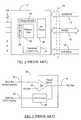
- FIG. 2is a simplified diagram illustrating a portion of the I/O circuit 36 in the memory chip 12 shown in FIG. 1 .
- the I/O circuit 36is shown to include two signal processing circuits—an output driver unit 38 , and an ODT (on die termination) circuit 40 . Both of these signal processing circuits are shown connected to the data (DQ) pins 18 of the memory chip 12 .
- the output driver 38is shown to be directly connected to an external clock pin 42 (which is one of the pins 24 on the chip 12 ) to receive an output enable signal therethrough. However, in practice, there may be additional intervening circuits between the clock pin 42 and the output driver 38 to generate appropriate output enable signal to be supplied to the driver 38 .
- the driver 38also receives the data signals (DQ Out) 43 from the memory cells 26 to be output on the DQ pins 18 (e.g., during a memory read operation).
- DQ Out signals 43are generated internally within the chip 12 as shown in FIG. 2 .
- FIG. 3illustrates an exemplary circuit layout of the output driver circuit 38 .
- the DQ Out 43 signalsare sent to the DQ pins 18 via the output driver 38 when the output enable signal 42 is active (e.g., active “high” in the implementation of FIG. 3 ).
- the output driver 38provides necessary signal amplification and buffering to the data signals to be sent from the memory cells 26 to the DQ pins 18 .
- Each output driver 38may have an IC (integrated circuit) output pad 46 to convey the data signals to the corresponding DQ pins 18 as is known in the art.
- the reference numeral “ 42 ”is used to interchangeably refer to the clock pin and the output enable signal.
- the clock input at pin 42may not directly be used as the output enable signal, but may get processed through intervening digital logic (not shown) to obtain the output enable signal as is known in the art.
- the I/O circuitmay also include the on-chip ODT circuit 40 to improve signal integrity in the system.
- An ODT pin 44(one of the pins 24 on the chip 12 ) may be provided on the chip to receive an externally-supplied (e.g., by a memory controller) ODT enable signal to activate the ODT circuit 40 .
- the ODT circuit 40 in FIG. 2is shown connected to the DQ pins 18 , in practice, corresponding ODT circuits 40 may be provided for any other pins on the chip 12 including, for example, the address pins 17 and the control pins 19 .
- the ODT circuit 40may be more prevalent in DDR (Double Data Rate) SDRAMs (Synchronous Dynamic Random Access Memories).
- the ODT circuit 40provides desired termination impedance to improve signal integrity by controlling reflected noise on the transfer line connecting the memory chip 12 to another processing device, e.g., a memory controller (not shown).
- a memory controllere.g., a memory controller
- the termination register(not shown) that was conventionally mounted on a motherboard carrying memory chips is incorporated inside the DDR SDRAM chip (e.g., as part of the test mode control unit 34 ) to enable or disable the ODT circuit 40 when desired.
- the termination registermay be programmed through the ODT pin 44 by an external processor (e.g., a memory controller) to enable/disable the ODT circuit 40 .
- the ODT circuit 40 in the other chip(which is not receiving data) is activated to absorb any signal propagations or reflections received on the data lines 18 (or address or control lines) of that “inactive” chip.
- This selective activation/deactivation of the ODT circuit 40e.g., in the memory chip that is not currently sending or receiving data
- the ODT circuit 40thus improves signal (e.g., data signals) integrity in the memory chip 12 .
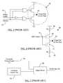
- FIG. 4depicts an exemplary circuit diagram of the ODT circuit 40 .
- the ODT circuit 40may include two identical termination resistors RT 48 - 49 whose values may be adjusted (e.g., by the external memory controller (not shown) through programming of the termination register (not shown)) depending on the desired termination.
- the termination resistors R T 48 - 49may not be strictly passive, fixed-value resistors. It is known that the termination value of R T 48 - 49 may be equal to the Thevenin equivalent of the resistors that terminate the DQ pins 18 at the IC output pad 52 .
- the ODT circuit 40may also include two switching elements—the “pull-up” n-channel CMOS transistor 50 and the “pull-down” n-channel CMOS transistor 51 . Proper biasing for the ODT circuit 40 may be provided as indicated and as is known in the art. As mentioned earlier, the ODT circuit 40 is activated when the ODT Enable signal 44 goes “high” (in the implementation of FIG. 4 ) and deactivated when the signal 44 is in the “low” state. It is observed that, for the sake of simplicity, the reference numeral “ 44 ” is used to interchangeably refer to the ODT pin and the ODT Enable signal. In practice, the signal received on the ODT pin may be processed by intervening logic circuitry (not shown) to generate the desired ODT Enable signal.
- FIG. 5shows an exemplary block diagram illustrating how a test mode related signal 56 is traditionally output to the DQ pins 18 of the memory 12 in FIG. 1 .
- test mode related signalis used to refer to any signal present on chip or on the die of an electronic device (e.g., the memory chip 12 ) and which is desired to be monitored by an external controller (e.g., a processor or memory controller (not shown)) during testing of the operation of the electronic device.
- an external controllere.g., a processor or memory controller (not shown)
- Athe information transfer during the testing operation is distinct from and may not be part of the routine data transfer during typical memory read/write operations.
- the test mode related signals 56may include various data outputs (DQ Out 43 ), output from one or more redundant elements on the chip 12 (e.g., a redundant row of memory cells to replace a current row of memory cells when one or more cells in the current row are defective, or a redundant column of memory cells, etc.), signals generated by a DLL (delay locked loop) or other clock generation circuits on the chip, various control signals such as shift left (SL), shift right (SR), Reset, DLL coarse shift, DLL fine shift, etc. These signals may need to be monitored in the event of a malfunction of the chip 12 , to debug the chip functionality or to ascertain operational defects in the chip 12 during testing of the chip.
- DQ Out 43data outputs
- SLshift left
- SRshift right
- ResetDLL coarse shift
- DLL fine shiftetc.
- a test mode related signal 56is output over DQ pins 18 to an “inquiring” device (e.g., the test processor or memory controller (not shown)) via the corresponding output driver circuit 38 as shown in FIG. 5 .
- the test processor or memory controllermay instruct the test mode control unit 34 to enable the output driver 38 to propagate appropriate signal “A” to the data output pins 18 .
- circuit details of such test mode signal transfers in FIG. 5are not shown here, it is observed that one or more signals from the control unit 34 and the signal “A” 56 may be processed through a digital circuit (not shown) prior to being applied to the output driver 38 to be output to the DQ pins 18 .
- test mode-specific output driversi.e., output drivers dedicated to transmit only signals “A” 56 —as part of the I/O circuit 36 on the chip 12 would result in additional capacitive loading at the DQ pins 18 used for test mode related signal transfers, thereby further affecting the speed with which output can be obtained.
- the on chip placement of such extra output driverswould also result in unnecessary waste of chip real estate.
- test mode related signal transfer mechanismthat does not add capacitance to output pins and also not affect the output speed path of signals output from the electronic device. It is further desirable to obtain such signal transfer mechanism without significantly adding logic circuitry on the chip real estate.
- the present disclosurecontemplates a method of operating an electronic device.
- the methodcomprises selecting an on die termination(ODT) circuit in the electronic device; and using only the selected ODT circuit to propagate a test mode related signal from said electronic device.
- ODTon die termination
- the present disclosurecontemplates an electronic device that comprises an ODT circuit having two inputs and an output; and a gate circuit coupled to the ODT circuit and configured to supply a test mode related signal to one of the two inputs so as to toggle the output of the ODT circuit in response to the test mode related signal, wherein the test mode related signal includes a signal present in the electronic device to allow testing thereof.
- the present disclosurecontemplates a memory device that comprises a plurality of memory cells to store data; and an I/O circuit configured to facilitate a data read/write operation from/to one or more of the plurality of memory cells, wherein the I/O circuit includes an ODT circuit, and a gate circuit coupled to the ODT circuit and configured to input a test mode related signal thereto so as to generate an output signal representative of the test mode related signal at an output of the ODT circuit, wherein the test mode related signal includes a signal present in the memory device to allow testing thereof.
- an electronic devicesuch as a memory chip
- One or more test mode related signalswhich include on-die signals and other relevant information, may be transferred from the integrated circuit of the electronic device to an external processor using the device's ODT circuit instead of the output data signal driver circuit. Therefore, no capacitive loading of output drivers occurs during test mode operations.
- the speed of the output data pathi.e., the circuit path propagating non-test mode related signals from the electronic device to other external units in the system
- the use of a minimal number of logic gates along with the existing ODT circuits to perform transmission of test mode related signalssubstantially maximizes chip real estate utilization without waste.
- FIG. 1is a simplified block diagram showing a memory chip or memory device
- FIG. 2is a simplified diagram illustrating a portion of the I/O circuit in the memory chip shown in FIG. 1 ;
- FIG. 3illustrates an exemplary circuit layout of the output driver circuit shown in FIG. 2 ;
- FIG. 4depicts an exemplary circuit diagram of the ODT circuit shown in FIG. 2 ;
- FIG. 5shows an exemplary block diagram illustrating how a test mode related signal is traditionally output to the DQ pins of the memory in FIG. 1 ;
- FIG. 6depicts an exemplary block diagram illustrating how the test mode related signal is output to the DQ pins according to one embodiment of the present disclosure
- FIG. 7illustrates an exemplary circuit configuration for the test mode signal transfer block diagram illustrated in FIG. 6 ;
- FIG. 8is a simplified block diagram showing a memory chip in communication with a memory controller, wherein the memory chip employs the test mode signal transfer mechanism illustrated by way of an example in FIG. 6 ;
- FIG. 9is a block diagram depicting a system in which one or more memory chips illustrated in FIG. 8 may be used.
- FIG. 6depicts an exemplary block diagram illustrating how the test mode related signal 56 is output to the DQ pins 18 according to one embodiment of the present disclosure.
- the test mode related signal 56 and a test mode enable signalare input to the ODT circuit 40 , which transfers the signal “A” 56 to the DQ pins 18 .
- the methodology of the present disclosureuses the already existing ODT circuit 40 in the I/O unit 36 to perform the signal transfer operation. It is noted here that the inputs to the ODT circuit 40 may not be supplied directly from the respective sources, but may be supplied through a gate circuit (discussed below with reference to FIG.
- the ODT circuit 40may form a part of the output driver 38 , however, in that case, only the ODT circuit 40 portion of the output driver 38 will be used to output test mode related signals 56 .
- FIG. 7illustrates an exemplary circuit configuration 60 for the test mode signal transfer block diagram illustrated in FIG. 6 .
- the ODT circuit 40(similar to that shown in FIG. 4 ) is shown to have its two inputs 57 - 58 connected to a gate circuit that includes two OR gates 62 - 63 , two AND gates 66 - 67 , and an inverter 68 . Three signals are input to the gate circuit—the test mode related signal 56 , the ODT enable signal 44 (also shown in FIGS. 2 and 4 ), and a test mode enable (TM) signal 70 .
- the IC output pad 52 of the ODT circuit 40may connect to the DQ pins 18 as shown in FIG. 7 .
- non-data related pinsmay also have ODT circuit 40 connected thereto for proper termination of unwanted or reflected signals in the system in operation.
- one or more of those non-data related pinsmay be used instead of or along with the DQ pins 18 to obtain the test mode related signal 56 .
- the ODT circuit(s) 40 associated with those non-data related pinsmay be used to propagate the on-chip signal “A” 56 out of the chip 12 . Therefore, in such configuration, the output pad 52 of the ODT circuit 40 may connect to other non-data related pins (not shown in FIG. 7 ). It is further observed that more than one ODT circuit 40 may be used to transfer different test mode related signals 56 over different pins 24 with which those ODT circuits 40 are associated.
- the test mode enable (TM) signal 70may be supplied by the test mode control unit 34 .
- the TM signal 70is a user-controlled signal generated internally within the chip 12 by appropriate programming of one or more test mode registers (not shown) in the control unit 34 .
- the programming of the test mode register(s)may be carried out by an external processor (e.g., a memory controller 80 shown in FIG. 8 ) using one or more address 17 and/or control lines 19 .
- output of the DLL clockmay be designated as “Test Mode-1”
- the output of a DLL coarse shift left signalmay be designated as “Test Mode-2”, etc.
- corresponding test mode register locationsmay be programmed to identify these test modes when requested by the external processor.
- the test mode control unit 34may be pre-programmed during memory fabrication, however, that programming may be changed later during testing using proper commands from the external processor.
- the TM signal 70is generated by the test mode control unit 34 when appropriate test mode—i.e., a test mode that is recognized by the control unit 34 either through the information already stored therein or provided by the external processor—is requested by the external processor using, for example, one or more of address 17 and/or control lines 19 .
- the generation of the TM signal 70is user-controlled in the sense that a user may externally control (e.g., using a test processor or memory controller) when the chip 12 should enter the test mode and, hence, when the test mode control unit 34 should commence supplying the test mode enable signals.
- the test mode control unit 34may raise the normally low TM signal 70 ( FIG. 7 ) to high or logic “1” state.
- the TM signal 70acts as a gating signal to gate the test mode related signal 56 to appropriate “leg” of the ODT circuit 40 .
- the transistor 50 and resistor 48may be considered to form the “pull up leg” of the ODT circuit 40
- the transistor 51 and resistor 49may be considered to form the “pull down leg” of the ODT circuit 40 .
- the TM signal 70remains high, whereas the ODT Enable signal 44 remains low to allow propagation of signal “A” 56 outside of the device through the appropriate leg of the ODT circuit 40 .
- the output signal appearing at the pad 52is thus related to the signal “A” 56 , which toggles individual legs of the ODT circuit 40 depending on whether signal “A” is high or low as can be seen from the circuit layout 60 in FIG. 7 . For example, when signal “A” 56 is high, it will turn on the transistor 50 but turn off transistor 51 , thus the output at the pad 52 will be “pulled up” or high because of the activation of the pull-up leg of the ODT circuit 40 .
- test mode related signal 56will toggle the ODT circuit 40 when test mode is asserted by raising the TM signal 70 to the high state.
- the ODT Enable signal 44is held normally low. However, because the ODT circuit 40 is used in FIG. 7 in a shared manner for test mode signal propagation as well as for routine signal termination applications, when a signal termination application is desired, the ODT Enable signal 44 (supplied through the ODT pin 44 ) may be raised high or in logic “1” state to activate both of the transistors 50 - 51 in the ODT circuit 40 for external signal absorption and termination. When the ODT Enable signal 44 is high, the test mode may not be performed because the values of the TM signal 70 and signal “A” 56 are immaterial because these values do not affect the operation of the ODT circuit 40 . Therefore, it may be preferable to not to perform testing while the ODT Enable signal 44 is active.
- the testingmay take place simultaneously or together with data transfer from memory cells 26 because the output driver 38 is no longer shared for the testing operation.
- the ODT circuit 40may transfer signals “A” 56 to appropriate output pins 24 whereas the output driver 38 may simultaneously transfer data signals to DQ pins 18 .
- FIG. 8is a simplified block diagram showing a memory chip 72 in communication with a memory controller 80 , wherein the memory chip employs the test mode signal transfer mechanism 60 illustrated by way of an example in FIG. 6 .
- the memory chip 72can be a dynamic random access memory (DRAM) or another type of memory circuits such as SRAM (Static Random Access Memory) or Flash memories.
- DRAMdynamic random access memory
- SRAMStatic Random Access Memory
- Flash memoriesFlash memories
- the DRAMcould be a synchronous DRAM commonly referred to as SGRAM (Synchronous Graphics Random Access Memory), SDRAM (Synchronous Dynamic Random Access Memory), SDRAM II, or DDR SDRAM (Double Data Rate SDRAM), as well as Synchlink or Rambus DRAMs.
- SGRAMSynchronous Graphics Random Access Memory
- SDRAMSerial Dynamic Random Access Memory
- SDRAM IISecure Digital Random Access Memory
- DDR SDRAMDouble Data Rate SDRAM
- test mode control unit 34 in memory chip 72may be different from the control unit 34 in chip 12 to take into account the new test mode signal transfer mechanism 60 in the I/O circuit 74 .
- units with similar functionalityare denoted by same reference numerals in FIGS. 1 and 8 .
- the memory controller 80can be a microprocessor, digital signal processor, embedded processor, micro-controller, dedicated memory test chip, a tester platform, or the like.
- the memory controller 80may control routine data transfer operations to/from the memory 72 , for example, when the memory is part of an operational computing system (not shown).
- the memory controller 80may initiate and carryout memory testing using the test mode control unit 34 , the I/O unit 74 (i.e., the ODT circuit-based test mode signal transfer mechanism 60 in the I/O unit 74 ), and one or more of the memory pins 24 as discussed hereinbefore at various places in the present disclosure.
- the memory controller 80may reside on the same motherboard (not shown) as that carrying the memory chip 72 .
- the memory controller 80may be a remote entity communicating with the memory chip 72 via a data transfer or communications network (e.g., a LAN (local area network) of computing devices).
- a data transfer or communications networke.g., a LAN (local area network) of computing devices.
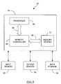
- FIG. 9is a block diagram depicting a system 82 in which one or more memory chips 72 illustrated in FIG. 8 may be used.
- the system 82may include a data processing unit or computing unit 84 that includes a processor 86 for performing various computing functions, such as executing specific software to perform specific calculations or data processing tasks.
- the computing unit 84also includes the memory controller 80 that is in communication with the processor 86 through a bus 88 .
- the bus 88may include an address bus (not shown), a data bus (not shown), and a control bus (not shown).
- the memory controller 80is also in communication with a set of memory devices 72 (i.e., multiple memory chips 72 of the type shown in FIG. 8 ) through another bus 90 .
- each memory device 72is a DDRII DRAM.
- Each memory device 72may include appropriate data storage and retrieval circuitry (not shown in FIG. 9 ) as shown in FIG. 8 .
- the processor 86can perform a plurality of functions based on information and data stored in the memories 72 .
- the system 82may include one or more input devices 92 (e.g., a keyboard or a mouse) connected to the computing unit 84 to allow a user to manually input data, instructions, etc., to operate the computing unit 84 .
- One or more output devices 94 connected to the computing unit 84may also be provided as part of the system 82 to display or otherwise output data generated by the processor 86 .
- Examples of output devices 94include printers, video terminals or video display units (VDUs).
- the system 82also includes one or more data storage devices 96 connected to the data processing unit 84 to allow the processor 86 to store data in or retrieve data from internal or external storage media (not shown).
- Examples of typical data storage devices 96include drives that accept hard and floppy disks, CD-ROMs (compact disk read-only memories), and tape cassettes.
- the memory devices 72 in the computing unit 84have the configuration illustrated in FIG. 8 , i.e., each memory device 72 includes an ODT-based test mode related signal transfer mechanism 60 depicted in FIG. 7 .
- an ODT circuit in a solid state electronic devicemay be used to transmit any other signal (whether test mode related or not) out of the device without using an output driver or similar signal output circuit.
- the ODT circuitmay be used in a manner similar to that discussed hereinbefore with reference to FIG. 7 to transmit an on-chip test mode related signal.
- test mode related signalswhich include on-die signals and other relevant information, may be transferred from the integrated circuit of the electronic device to an external processor using the device's ODT circuit instead of the output data signal driver circuit. Therefore, no capacitive loading of output drivers occurs during test mode operations. Thus the speed of the output data path (i.e., the circuit path propagating non-test mode related signals from the electronic device to other external units in the system) is not affected by test mode operations, allowing a system designer to increase the speed of the data output path as much as desired. Further, deterioration in the quality of signals output from the output drivers is also avoided. Also, the use of a minimal number of logic gates along with the existing ODT circuits to perform transmission of test mode related signals substantially maximizes chip real estate utilization without waste.
Landscapes
- Tests Of Electronic Circuits (AREA)
- For Increasing The Reliability Of Semiconductor Memories (AREA)
- Semiconductor Integrated Circuits (AREA)
Abstract
Description
- 1. Field of the Disclosure
- The present disclosure generally relates to testing of electronic devices and, more particularly, to a system and method to test semiconductor memory chips.
- 2. Brief Description of Related Art
- Memory devices are widely used in many electronic products and computers to store data. A memory device is a semiconductor electronic device that includes a number of memory cells, each cell storing one bit of data. The data stored in the memory cells can be read during a read operation.
FIG. 1 is a simplified block diagram showing a memory chip ormemory device 12. Thememory chip 12 may be part of a DIMM (dual in-line memory module) or a PCB (printed circuit board) containing many such memory chips (not shown inFIG. 1 ). Thememory chip 12 may include a plurality ofpins 24 located outside ofchip 12 for electrically connecting thechip 12 to other system devices. Some of thosepins 24 may constitute memory address pins oraddress bus 17, data (DQ) pins ordata bus 18, and control pins orcontrol bus 19. It is evident that each of the reference numerals17-19 designates more than one pin in the corresponding bus. Further, it is understood that the schematic inFIG. 1 is for illustration only. That is, the pin arrangement or configuration in a typical memory chip may not be in the form shown inFIG. 1 . - A processor or memory controller (not shown) may communicate with the
chip 12 and perform memory read/write operations. The processor and thememory chip 12 may communicate using address signals on the address lines oraddress bus 17, data signals on the data lines ordata bus 18, and control signals (e.g., a row address select (RAS) signal, a column address select (CAS) signal, etc. (not shown)) on the control lines orcontrol bus 19. The “width” (i.e., number of pins) of address, data and control buses may differ from one memory configuration to another. - Those of ordinary skill in the art will readily recognize that
memory chip 12 ofFIG. 1 is simplified to illustrate one embodiment of a memory chip and is not intended to be a detailed illustration of all of the features of a typical memory chip. Numerous peripheral devices or circuits may be typically provided along with thememory chip 12 for writing data to and reading data from thememory cells 26. However, these peripheral devices or circuits are not shown inFIG. 1 for the sake of clarity. - The
memory chip 12 may include a plurality ofmemory cells 26 generally arranged in rows and columns to store data in rows and columns. Arow decode circuit 28 and acolumn decode circuit 30 may select the rows and columns in thememory cells 26 in response to decoding an address, provided on theaddress bus 17. Data to/from thememory cells 26 is then transferred over thedata bus 18 via sense amplifiers and a data output path (not shown). A memory controller (not shown) may provide relevant control signals (not shown) on thecontrol bus 19 to control data communication to and from thememory chip 12 via an I/O (input/output)circuit 36. The I/O circuit 36 may include a number of data output buffers to receive the data bits from thememory cells 26 and provide those data bits or data signals to the corresponding data lines in thedata bus 18. An exemplary I/O circuit is discussed below with reference toFIG. 2 . - The memory controller (not shown) may determine the modes of operation of
memory chip 12. Some examples of the input signals or control signals (not shown inFIG. 1 ) on thecontrol bus 19 include an External Clock signal, a Chip Select signal, a Row Access Strobe signal, a Column Access Strobe signal, a Write Enable signal, etc. Thememory chip 12 communicates to other devices connected thereto via thepins 24 on thechip 12. These pins, as mentioned before, may be connected to appropriate address, data and control lines to carry out data transfer (i.e., data transmission and reception) operations. - A test
mode control unit 34 is also illustrated as part of thememory chip 12. The testmode control unit 34 may include digital logic such as, for example, one or more test mode registers to perform testing of thememory chip 12 to obtain information about various signals generated within thechip 12 as discussed later. A memory controller (not shown) may instruct thecontrol unit 34 to supply the requested test mode related signal information from thechip 12. FIG. 2 is a simplified diagram illustrating a portion of the I/O circuit 36 in thememory chip 12 shown inFIG. 1 . The I/O circuit 36 is shown to include two signal processing circuits—anoutput driver unit 38, and an ODT (on die termination)circuit 40. Both of these signal processing circuits are shown connected to the data (DQ)pins 18 of thememory chip 12. Theoutput driver 38 is shown to be directly connected to an external clock pin42 (which is one of thepins 24 on the chip12) to receive an output enable signal therethrough. However, in practice, there may be additional intervening circuits between theclock pin 42 and theoutput driver 38 to generate appropriate output enable signal to be supplied to thedriver 38. Thedriver 38 also receives the data signals (DQ Out)43 from thememory cells 26 to be output on the DQ pins18 (e.g., during a memory read operation). Thus, theDQ Out signals 43 are generated internally within thechip 12 as shown inFIG. 2 .FIG. 3 illustrates an exemplary circuit layout of theoutput driver circuit 38. As is known in the art and as can be seen fromFIG. 3 , the DQ Out43 signals are sent to theDQ pins 18 via theoutput driver 38 when the output enablesignal 42 is active (e.g., active “high” in the implementation ofFIG. 3 ). Once enabled, theoutput driver 38 provides necessary signal amplification and buffering to the data signals to be sent from thememory cells 26 to theDQ pins 18. There may be more than oneoutput driver 38 in thememory chip 12—oneoutput driver 38 for eachdata line 18. Eachoutput driver 38 may have an IC (integrated circuit)output pad 46 to convey the data signals to thecorresponding DQ pins 18 as is known in the art. It is noted here that, for the sake of simplicity, the reference numeral “42” is used to interchangeably refer to the clock pin and the output enable signal. In practice, the clock input atpin 42 may not directly be used as the output enable signal, but may get processed through intervening digital logic (not shown) to obtain the output enable signal as is known in the art.- Referring again to
FIG. 2 , it is seen that the I/O circuit may also include the on-chip ODT circuit 40 to improve signal integrity in the system. An ODT pin44 (one of thepins 24 on the chip12) may be provided on the chip to receive an externally-supplied (e.g., by a memory controller) ODT enable signal to activate theODT circuit 40. Although theODT circuit 40 inFIG. 2 is shown connected to theDQ pins 18, in practice,corresponding ODT circuits 40 may be provided for any other pins on thechip 12 including, for example, theaddress pins 17 and thecontrol pins 19. TheODT circuit 40 may be more prevalent in DDR (Double Data Rate) SDRAMs (Synchronous Dynamic Random Access Memories). - In operation, the
ODT circuit 40 provides desired termination impedance to improve signal integrity by controlling reflected noise on the transfer line connecting thememory chip 12 to another processing device, e.g., a memory controller (not shown). In a DDR SDRAM, the termination register (not shown) that was conventionally mounted on a motherboard carrying memory chips is incorporated inside the DDR SDRAM chip (e.g., as part of the test mode control unit34) to enable or disable theODT circuit 40 when desired. The termination register may be programmed through theODT pin 44 by an external processor (e.g., a memory controller) to enable/disable theODT circuit 40. As is known in the art, for example, when twomemory chips 12 are loaded in a system, then during a memory write operation to one of thechips 12, theODT circuit 40 in the other chip (which is not receiving data) is activated to absorb any signal propagations or reflections received on the data lines18 (or address or control lines) of that “inactive” chip. This selective activation/deactivation of the ODT circuit40 (e.g., in the memory chip that is not currently sending or receiving data) prevents the “inactive” chip from receiving spurious signals, thereby avoiding data corruption in the chip. TheODT circuit 40 thus improves signal (e.g., data signals) integrity in thememory chip 12. FIG. 4 depicts an exemplary circuit diagram of theODT circuit 40. TheODT circuit 40 may include two identical termination resistors RT48-49 whose values may be adjusted (e.g., by the external memory controller (not shown) through programming of the termination register (not shown)) depending on the desired termination. Thus, the termination resistors RT48-49 may not be strictly passive, fixed-value resistors. It is known that the termination value of RT48-49 may be equal to the Thevenin equivalent of the resistors that terminate theDQ pins 18 at theIC output pad 52. TheODT circuit 40 may also include two switching elements—the “pull-up” n-channel CMOS transistor 50 and the “pull-down” n-channel CMOS transistor 51. Proper biasing for theODT circuit 40 may be provided as indicated and as is known in the art. As mentioned earlier, theODT circuit 40 is activated when theODT Enable signal 44 goes “high” (in the implementation ofFIG. 4 ) and deactivated when thesignal 44 is in the “low” state. It is observed that, for the sake of simplicity, the reference numeral “44” is used to interchangeably refer to the ODT pin and the ODT Enable signal. In practice, the signal received on the ODT pin may be processed by intervening logic circuitry (not shown) to generate the desired ODT Enable signal.FIG. 5 shows an exemplary block diagram illustrating how a test mode relatedsignal 56 is traditionally output to the DQ pins18 of thememory 12 inFIG. 1 . In the discussion hereinbelow, the term “test mode related signal” is used to refer to any signal present on chip or on the die of an electronic device (e.g., the memory chip12) and which is desired to be monitored by an external controller (e.g., a processor or memory controller (not shown)) during testing of the operation of the electronic device. For convenience, such signal is referred to by letter “A” in the discussion below. It is noted here that the information transfer during the testing operation is distinct from and may not be part of the routine data transfer during typical memory read/write operations. The test mode relatedsignals 56 may include various data outputs (DQ Out43), output from one or more redundant elements on the chip12 (e.g., a redundant row of memory cells to replace a current row of memory cells when one or more cells in the current row are defective, or a redundant column of memory cells, etc.), signals generated by a DLL (delay locked loop) or other clock generation circuits on the chip, various control signals such as shift left (SL), shift right (SR), Reset, DLL coarse shift, DLL fine shift, etc. These signals may need to be monitored in the event of a malfunction of thechip 12, to debug the chip functionality or to ascertain operational defects in thechip 12 during testing of the chip.- Traditionally, a test mode related
signal 56 is output over DQ pins18 to an “inquiring” device (e.g., the test processor or memory controller (not shown)) via the correspondingoutput driver circuit 38 as shown inFIG. 5 . The test processor or memory controller (not shown) may instruct the testmode control unit 34 to enable theoutput driver 38 to propagate appropriate signal “A” to the data output pins18. Although circuit details of such test mode signal transfers inFIG. 5 are not shown here, it is observed that one or more signals from thecontrol unit 34 and the signal “A”56 may be processed through a digital circuit (not shown) prior to being applied to theoutput driver 38 to be output to the DQ pins18. - In the arrangement of
FIG. 5 , to communicate internal chip signals to an outside controller (e.g., a memory controller (not shown)), the use of variouscorresponding output drivers 38 and testing related circuitry coupled to thesedrivers 38 results in addition of capacitance to the external pins24 (e.g., DQ pins18) through which signals “A”56 are obtained. Also, such “loading” ofoutput drivers 38 by testing related logic circuitry negatively affects chip performance during routine high speed data transfer operations (e.g., typical memory read/write operations during run time). For example, more gates added tooutput drivers 38 for testing related circuitry may not only result in additional output delays, but may also cause jitter on output signals and may significantly deteriorate quality of output signals. Furthermore, as clock speed of electronic devices (e.g., memory chips) increases, any addition of test mode-specific output drivers—i.e., output drivers dedicated to transmit only signals “A”56—as part of the I/O circuit 36 on thechip 12 would result in additional capacitive loading at the DQ pins18 used for test mode related signal transfers, thereby further affecting the speed with which output can be obtained. The on chip placement of such extra output drivers would also result in unnecessary waste of chip real estate. - Therefore, it is desirable to devise a test mode related signal transfer mechanism that does not add capacitance to output pins and also not affect the output speed path of signals output from the electronic device. It is further desirable to obtain such signal transfer mechanism without significantly adding logic circuitry on the chip real estate.
- The present disclosure contemplates a method of operating an electronic device. The method comprises selecting an on die termination(ODT) circuit in the electronic device; and using only the selected ODT circuit to propagate a test mode related signal from said electronic device.
- In one embodiment, the present disclosure contemplates an electronic device that comprises an ODT circuit having two inputs and an output; and a gate circuit coupled to the ODT circuit and configured to supply a test mode related signal to one of the two inputs so as to toggle the output of the ODT circuit in response to the test mode related signal, wherein the test mode related signal includes a signal present in the electronic device to allow testing thereof.
- In another embodiment, the present disclosure contemplates a memory device that comprises a plurality of memory cells to store data; and an I/O circuit configured to facilitate a data read/write operation from/to one or more of the plurality of memory cells, wherein the I/O circuit includes an ODT circuit, and a gate circuit coupled to the ODT circuit and configured to input a test mode related signal thereto so as to generate an output signal representative of the test mode related signal at an output of the ODT circuit, wherein the test mode related signal includes a signal present in the memory device to allow testing thereof.
- According to a system and method of the present disclosure an electronic device, such as a memory chip, is operated in a test mode using the device's built-in ODT circuit. One or more test mode related signals, which include on-die signals and other relevant information, may be transferred from the integrated circuit of the electronic device to an external processor using the device's ODT circuit instead of the output data signal driver circuit. Therefore, no capacitive loading of output drivers occurs during test mode operations. Thus the speed of the output data path (i.e., the circuit path propagating non-test mode related signals from the electronic device to other external units in the system) is not affected by test mode operations, allowing a system designer to increase the speed of the data output path as much as desired. Also, the use of a minimal number of logic gates along with the existing ODT circuits to perform transmission of test mode related signals substantially maximizes chip real estate utilization without waste.
- For the present disclosure to be easily understood and readily practiced, the present disclosure will now be described for purposes of illustration and not limitation, in connection with the following figures, wherein:
FIG. 1 is a simplified block diagram showing a memory chip or memory device;FIG. 2 is a simplified diagram illustrating a portion of the I/O circuit in the memory chip shown inFIG. 1 ;FIG. 3 illustrates an exemplary circuit layout of the output driver circuit shown inFIG. 2 ;FIG. 4 depicts an exemplary circuit diagram of the ODT circuit shown inFIG. 2 ;FIG. 5 shows an exemplary block diagram illustrating how a test mode related signal is traditionally output to the DQ pins of the memory inFIG. 1 ;FIG. 6 depicts an exemplary block diagram illustrating how the test mode related signal is output to the DQ pins according to one embodiment of the present disclosure;FIG. 7 illustrates an exemplary circuit configuration for the test mode signal transfer block diagram illustrated inFIG. 6 ;FIG. 8 is a simplified block diagram showing a memory chip in communication with a memory controller, wherein the memory chip employs the test mode signal transfer mechanism illustrated by way of an example inFIG. 6 ; andFIG. 9 is a block diagram depicting a system in which one or more memory chips illustrated inFIG. 8 may be used.- Reference will now be made in detail to some embodiments of the present disclosure, examples of which are illustrated in the accompanying drawings. It is to be understood that the figures and descriptions of the present disclosure included herein illustrate and describe elements that are of particular relevance to the present disclosure, while eliminating, for the sake of clarity, other elements found in typical solid-state electronic devices, memories or memory-based systems. It is noted at the outset that the terms “connected”, “connecting,” “electrically connected,” etc., are used interchangeably herein to generally refer to the condition of being electrically connected. It is further noted that various block diagrams and circuit diagrams shown and discussed herein employ logic circuits that implement positive logic, i.e., a high value on a signal is treated as a logic “1” whereas a low value is treated as a logic “0.” However, any of the circuit discussed herein may be easily implemented in negative logic (i.e., a high value on a signal is treated as a logic “0” whereas a low value is treated as a logic “1”).
FIG. 6 depicts an exemplary block diagram illustrating how the test mode relatedsignal 56 is output to the DQ pins18 according to one embodiment of the present disclosure. The test mode relatedsignal 56 and a test mode enable signal (discussed later with reference toFIG. 7 ) are input to theODT circuit 40, which transfers the signal “A”56 to the DQ pins18. Thus, instead of loading theoutput driver 38 in the I/O unit 36, the methodology of the present disclosure uses the already existingODT circuit 40 in the I/O unit 36 to perform the signal transfer operation. It is noted here that the inputs to theODT circuit 40 may not be supplied directly from the respective sources, but may be supplied through a gate circuit (discussed below with reference toFIG. 7 ) to accommodate various signals associated with theODT circuit 40 without substantially adding additional logic circuits or increasing chip real estate. It is observed that only theODT circuit 40 is used to propagate the test mode relatedsignal 56 to the data output pins18, without using any portion of theoutput driver circuit 38. In one embodiment, theODT circuit 40 may form a part of theoutput driver 38, however, in that case, only theODT circuit 40 portion of theoutput driver 38 will be used to output test mode related signals56.FIG. 7 illustrates anexemplary circuit configuration 60 for the test mode signal transfer block diagram illustrated inFIG. 6 . The ODT circuit40 (similar to that shown inFIG. 4 ) is shown to have its two inputs57-58 connected to a gate circuit that includes two OR gates62-63, two AND gates66-67, and aninverter 68. Three signals are input to the gate circuit—the test mode relatedsignal 56, the ODT enable signal44 (also shown inFIGS. 2 and 4 ), and a test mode enable (TM)signal 70. TheIC output pad 52 of theODT circuit 40 may connect to the DQ pins18 as shown inFIG. 7 . However, as noted before, it is observed that non-data related pins (e.g., address pins17, control pins19, or any other pins from the set of pins24) may also haveODT circuit 40 connected thereto for proper termination of unwanted or reflected signals in the system in operation. Thus, one or more of those non-data related pins may be used instead of or along with the DQ pins18 to obtain the test mode relatedsignal 56. In that event, the ODT circuit(s)40 associated with those non-data related pins may be used to propagate the on-chip signal “A”56 out of thechip 12. Therefore, in such configuration, theoutput pad 52 of theODT circuit 40 may connect to other non-data related pins (not shown inFIG. 7 ). It is further observed that more than oneODT circuit 40 may be used to transfer different test mode relatedsignals 56 overdifferent pins 24 with which thoseODT circuits 40 are associated.- The test mode enable (TM)
signal 70 may be supplied by the testmode control unit 34. In one embodiment, theTM signal 70 is a user-controlled signal generated internally within thechip 12 by appropriate programming of one or more test mode registers (not shown) in thecontrol unit 34. The programming of the test mode register(s) may be carried out by an external processor (e.g., amemory controller 80 shown inFIG. 8 ) using one ormore address 17 and/or control lines19. For example, output of the DLL clock may be designated as “Test Mode-1”, the output of a DLL coarse shift left signal may be designated as “Test Mode-2”, etc., and corresponding test mode register locations may be programmed to identify these test modes when requested by the external processor. Alternatively, the testmode control unit 34 may be pre-programmed during memory fabrication, however, that programming may be changed later during testing using proper commands from the external processor. Thus, in the embodiment ofFIG. 7 , theTM signal 70 is generated by the testmode control unit 34 when appropriate test mode—i.e., a test mode that is recognized by thecontrol unit 34 either through the information already stored therein or provided by the external processor—is requested by the external processor using, for example, one or more ofaddress 17 and/or control lines19. Therefore, the generation of theTM signal 70 is user-controlled in the sense that a user may externally control (e.g., using a test processor or memory controller) when thechip 12 should enter the test mode and, hence, when the testmode control unit 34 should commence supplying the test mode enable signals. - Upon activation and upon receipt proper test mode request from the external processor, the test
mode control unit 34 may raise the normally low TM signal70 (FIG. 7 ) to high or logic “1” state. Thus, it is seen from the embodiment inFIG. 7 , that theTM signal 70 acts as a gating signal to gate the test mode relatedsignal 56 to appropriate “leg” of theODT circuit 40. InFIG. 7 , thetransistor 50 andresistor 48 may be considered to form the “pull up leg” of theODT circuit 40, whereas thetransistor 51 andresistor 49 may be considered to form the “pull down leg” of theODT circuit 40. During test mode, theTM signal 70 remains high, whereas theODT Enable signal 44 remains low to allow propagation of signal “A”56 outside of the device through the appropriate leg of theODT circuit 40. The output signal appearing at thepad 52 is thus related to the signal “A”56, which toggles individual legs of theODT circuit 40 depending on whether signal “A” is high or low as can be seen from thecircuit layout 60 inFIG. 7 . For example, when signal “A”56 is high, it will turn on thetransistor 50 but turn offtransistor 51, thus the output at thepad 52 will be “pulled up” or high because of the activation of the pull-up leg of theODT circuit 40. On the other hand, when the signal “A”56 goes low, it will instead turn ontransistor 51 and, hence, it will propagate to theoutput pad 52 as a low output signal via the pull-down leg of theODT circuit 40. Thus, the test mode relatedsignal 56 will toggle theODT circuit 40 when test mode is asserted by raising theTM signal 70 to the high state. - The
ODT Enable signal 44 is held normally low. However, because theODT circuit 40 is used inFIG. 7 in a shared manner for test mode signal propagation as well as for routine signal termination applications, when a signal termination application is desired, the ODT Enable signal44 (supplied through the ODT pin44) may be raised high or in logic “1” state to activate both of the transistors50-51 in theODT circuit 40 for external signal absorption and termination. When theODT Enable signal 44 is high, the test mode may not be performed because the values of theTM signal 70 and signal “A”56 are immaterial because these values do not affect the operation of theODT circuit 40. Therefore, it may be preferable to not to perform testing while theODT Enable signal 44 is active. - It is seen from the configuration in
FIGS. 6-7 that, in one embodiment, the testing may take place simultaneously or together with data transfer frommemory cells 26 because theoutput driver 38 is no longer shared for the testing operation. Thus, theODT circuit 40 may transfer signals “A”56 to appropriate output pins24 whereas theoutput driver 38 may simultaneously transfer data signals to DQ pins18. However, it may be preferable to perform testing when no data transfer activity is present, i.e., when thememory chip 12 is not operated in its routine data read/write mode, but rather exclusively in the test mode. - It is further seen from the configuration in
FIGS. 6-7 that theoutput drivers 38 are not affected by the test mode operations. Therefore, no capacitive loading ofoutput drivers 38 is present in the configuration ofFIGS. 6-7 . Thus the speed of the output data path (i.e., the circuit path propagating data (DQ) signals to DQ pins18) is not affected by test mode operations, allowing a system designer to increase the speed of the data output path as much as desired. Also, the use of a minimal number of logic gates along with the existingODT circuits 40 to perform transmission of test mode related signals (containing on-die information) substantially maximizes chip real estate utilization without wasteful use of chip real estate. FIG. 8 is a simplified block diagram showing amemory chip 72 in communication with amemory controller 80, wherein the memory chip employs the test modesignal transfer mechanism 60 illustrated by way of an example inFIG. 6 . Thememory chip 72 can be a dynamic random access memory (DRAM) or another type of memory circuits such as SRAM (Static Random Access Memory) or Flash memories. Furthermore, the DRAM could be a synchronous DRAM commonly referred to as SGRAM (Synchronous Graphics Random Access Memory), SDRAM (Synchronous Dynamic Random Access Memory), SDRAM II, or DDR SDRAM (Double Data Rate SDRAM), as well as Synchlink or Rambus DRAMs. Thecircuit configuration 60 inFIG. 7 may be part of the I/O circuit 74 in thememory chip 72. It is noted here that although other elements in thememory chip 72 are designated with the same reference numerals as those given inFIG. 1 , it may be possible that those components having same reference numerals may not be identical in thememories mode control unit 34 inmemory chip 72 may be different from thecontrol unit 34 inchip 12 to take into account the new test modesignal transfer mechanism 60 in the I/O circuit 74. However, for the sake of simplicity, units with similar functionality are denoted by same reference numerals inFIGS. 1 and 8 .- The
memory controller 80 can be a microprocessor, digital signal processor, embedded processor, micro-controller, dedicated memory test chip, a tester platform, or the like. Thememory controller 80 may control routine data transfer operations to/from thememory 72, for example, when the memory is part of an operational computing system (not shown). Alternatively or in addition to that configuration, thememory controller 80 may initiate and carryout memory testing using the testmode control unit 34, the I/O unit74 (i.e., the ODT circuit-based test modesignal transfer mechanism 60 in the I/O unit74), and one or more of the memory pins24 as discussed hereinbefore at various places in the present disclosure. Thememory controller 80 may reside on the same motherboard (not shown) as that carrying thememory chip 72. Various other configurations of electrical connection between thememory chip 72 and thememory controller 80 may be possible. For example, thememory controller 80 may be a remote entity communicating with thememory chip 72 via a data transfer or communications network (e.g., a LAN (local area network) of computing devices). FIG. 9 is a block diagram depicting asystem 82 in which one ormore memory chips 72 illustrated inFIG. 8 may be used. Thesystem 82 may include a data processing unit orcomputing unit 84 that includes aprocessor 86 for performing various computing functions, such as executing specific software to perform specific calculations or data processing tasks. Thecomputing unit 84 also includes thememory controller 80 that is in communication with theprocessor 86 through abus 88. Thebus 88 may include an address bus (not shown), a data bus (not shown), and a control bus (not shown). Thememory controller 80 is also in communication with a set of memory devices72 (i.e.,multiple memory chips 72 of the type shown inFIG. 8 ) through anotherbus 90. In one embodiment, eachmemory device 72 is a DDRII DRAM. Eachmemory device 72 may include appropriate data storage and retrieval circuitry (not shown inFIG. 9 ) as shown inFIG. 8 . Theprocessor 86 can perform a plurality of functions based on information and data stored in thememories 72. Thesystem 82 may include one or more input devices92 (e.g., a keyboard or a mouse) connected to thecomputing unit 84 to allow a user to manually input data, instructions, etc., to operate thecomputing unit 84. One ormore output devices 94 connected to thecomputing unit 84 may also be provided as part of thesystem 82 to display or otherwise output data generated by theprocessor 86. Examples ofoutput devices 94 include printers, video terminals or video display units (VDUs). In one embodiment, thesystem 82 also includes one or moredata storage devices 96 connected to thedata processing unit 84 to allow theprocessor 86 to store data in or retrieve data from internal or external storage media (not shown). Examples of typicaldata storage devices 96 include drives that accept hard and floppy disks, CD-ROMs (compact disk read-only memories), and tape cassettes. As noted before, thememory devices 72 in thecomputing unit 84 have the configuration illustrated inFIG. 8 , i.e., eachmemory device 72 includes an ODT-based test mode relatedsignal transfer mechanism 60 depicted inFIG. 7 .- It is observed that although the discussion given hereinbefore has been primarily with reference to memory devices and test mode related signal transfers in such devices, it is evident that the ODT-based signal transfer mechanism illustrated in
FIG. 7 may be employed, with suitable modifications which may be desirable by one skilled in the art to obtain the test mode related signals, in any non-memory electronic device that may need to be tested and that already has a built-inODT circuit 40 or a similar circuit configuration. Apart from the test mode related signal transfer discussed hereinabove, an ODT circuit in a solid state electronic device may be used to transmit any other signal (whether test mode related or not) out of the device without using an output driver or similar signal output circuit. In this application, the ODT circuit may be used in a manner similar to that discussed hereinbefore with reference toFIG. 7 to transmit an on-chip test mode related signal. - The foregoing describes a system and method to operate an electronic device, such as a memory chip, in a test mode using the device's built-in ODT (on die termination) circuit. One or more test mode related signals, which include on-die signals and other relevant information, may be transferred from the integrated circuit of the electronic device to an external processor using the device's ODT circuit instead of the output data signal driver circuit. Therefore, no capacitive loading of output drivers occurs during test mode operations. Thus the speed of the output data path (i.e., the circuit path propagating non-test mode related signals from the electronic device to other external units in the system) is not affected by test mode operations, allowing a system designer to increase the speed of the data output path as much as desired. Further, deterioration in the quality of signals output from the output drivers is also avoided. Also, the use of a minimal number of logic gates along with the existing ODT circuits to perform transmission of test mode related signals substantially maximizes chip real estate utilization without waste.
- While the disclosure has been described in detail and with reference to specific embodiments thereof, it will be apparent to one skilled in the art that various changes and modifications can be made therein without departing from the spirit and scope of the embodiments. Thus, it is intended that the present disclosure cover the modifications and variations of this disclosure provided they come within the scope of the appended claims and their equivalents.
Claims (28)
Priority Applications (2)
| Application Number | Priority Date | Filing Date | Title |
|---|---|---|---|
| US10/872,608US7574634B2 (en) | 2004-06-21 | 2004-06-21 | Real time testing using on die termination (ODT) circuit |
| US11/485,800US7664999B2 (en) | 2004-06-21 | 2006-07-13 | Real time testing using on die termination (ODT) circuit |
Applications Claiming Priority (1)
| Application Number | Priority Date | Filing Date | Title |
|---|---|---|---|
| US10/872,608US7574634B2 (en) | 2004-06-21 | 2004-06-21 | Real time testing using on die termination (ODT) circuit |
Related Child Applications (1)
| Application Number | Title | Priority Date | Filing Date |
|---|---|---|---|
| US11/485,800ContinuationUS7664999B2 (en) | 2004-06-21 | 2006-07-13 | Real time testing using on die termination (ODT) circuit |
Publications (2)
| Publication Number | Publication Date |
|---|---|
| US20050283671A1true US20050283671A1 (en) | 2005-12-22 |
| US7574634B2 US7574634B2 (en) | 2009-08-11 |
Family
ID=35481974
Family Applications (2)
| Application Number | Title | Priority Date | Filing Date |
|---|---|---|---|
| US10/872,608Expired - Fee RelatedUS7574634B2 (en) | 2004-06-21 | 2004-06-21 | Real time testing using on die termination (ODT) circuit |
| US11/485,800Expired - LifetimeUS7664999B2 (en) | 2004-06-21 | 2006-07-13 | Real time testing using on die termination (ODT) circuit |
Family Applications After (1)
| Application Number | Title | Priority Date | Filing Date |
|---|---|---|---|
| US11/485,800Expired - LifetimeUS7664999B2 (en) | 2004-06-21 | 2006-07-13 | Real time testing using on die termination (ODT) circuit |
Country Status (1)
| Country | Link |
|---|---|
| US (2) | US7574634B2 (en) |
Cited By (14)
| Publication number | Priority date | Publication date | Assignee | Title |
|---|---|---|---|---|
| US20050253615A1 (en)* | 2004-05-13 | 2005-11-17 | Jung Sunwoo | Parameter measurement of semiconductor device from pin with on die termination circuit |
| US20060126401A1 (en)* | 2004-12-10 | 2006-06-15 | Micron Technology, Inc. | Reducing DQ pin capacitance in a memory device |
| US20070030051A1 (en)* | 2005-07-19 | 2007-02-08 | Samsung Electronics Co., Ltd. | Signature circuit, semiconductor device having the same and method of reading signature information |
| US20070046308A1 (en)* | 2005-08-26 | 2007-03-01 | Ronald Baker | Test modes for a semiconductor integrated circuit device |
| US20080040081A1 (en)* | 2006-02-17 | 2008-02-14 | Elpida Memory, Inc. | Simulation method for improving freedom of setting parameters relating to input/output characteristics of a memory chip |
| US20080042684A1 (en)* | 2006-08-16 | 2008-02-21 | Hynix Semiconductor Inc. | Apparatus for controlling on-die termination of semiconductor memory and methods of controlling the same |
| WO2010096097A1 (en)* | 2008-10-30 | 2010-08-26 | Hewlett-Packard Development Company, L.P. | Differential on-line termination |
| WO2011041064A3 (en)* | 2009-10-01 | 2011-06-23 | Rambus Inc. | Methods and systems for reducing supply and termination noise |
| US8561001B1 (en)* | 2012-07-11 | 2013-10-15 | Taiwan Semiconductor Manufacturing Co., Ltd. | System and method for testing stacked dies |
| US20150162318A1 (en)* | 2013-12-10 | 2015-06-11 | Infineon Technologies Ag | Chip, chip package and die |
| US11354255B2 (en)* | 2019-06-04 | 2022-06-07 | Realtek Semiconductor Corporation | Processing chip having different modes and corresponding chip system and operation method of the same |
| US20220254375A1 (en)* | 2021-02-05 | 2022-08-11 | Fujifilm Corporation | Magnetic tape cartridge, magnetic tape drive, magnetic tape system, and method of operating magnetic tape drive |
| US11783859B2 (en)* | 2020-05-25 | 2023-10-10 | Fujifilm Corporation | Noncontact communication medium, magnetic tape cartridge, method for operating noncontact communication medium, and program |
| US12237030B2 (en)* | 2021-09-01 | 2025-02-25 | Changxin Memory Technologies, Inc. | Layout of driving circuit, semiconductor structure and semiconductor memory |
Families Citing this family (4)
| Publication number | Priority date | Publication date | Assignee | Title |
|---|---|---|---|---|
| KR101097447B1 (en)* | 2010-05-31 | 2011-12-23 | 주식회사 하이닉스반도체 | Data transmission device |
| KR20120005820A (en)* | 2010-07-09 | 2012-01-17 | 주식회사 하이닉스반도체 | Semiconductor device and its test method |
| JP5726828B2 (en)* | 2012-09-11 | 2015-06-03 | 株式会社東芝 | Output driver |
| US9912498B2 (en)* | 2015-03-05 | 2018-03-06 | Micron Technology, Inc. | Testing impedance adjustment |
Citations (20)
| Publication number | Priority date | Publication date | Assignee | Title |
|---|---|---|---|---|
| US4435803A (en)* | 1980-03-31 | 1984-03-06 | International Telephone And Telegraph Corporation | Analog subscriber/trunk module with shared ringing source and ring-trip |
| US6335632B1 (en)* | 2000-05-30 | 2002-01-01 | International Business Machines Corporation | CMOS small signal switchable terminator network |
| US20020188898A1 (en)* | 2001-06-08 | 2002-12-12 | Mitsubishi Denki Kabushiki Kaisha | Tester built-in semiconductor integrated circuit device |
| US6535047B2 (en)* | 2001-05-17 | 2003-03-18 | Intel Corporation | Apparatus and method to use a single reference component in a master-slave configuration for multiple circuit compensation |
| US6714038B2 (en)* | 2001-07-13 | 2004-03-30 | Samsung Electronics Co., Ltd. | Apparatus for controlling input termination of semiconductor memory device and method for the same |
| US6741095B2 (en)* | 2001-05-21 | 2004-05-25 | Aucid Corporation, Limited | Data transmission system, circuit and method |
| US6762620B2 (en)* | 2002-05-24 | 2004-07-13 | Samsung Electronics Co., Ltd. | Circuit and method for controlling on-die signal termination |
| US20040141391A1 (en)* | 2003-01-03 | 2004-07-22 | Dong-Jin Lee | Synchronous semiconductor memory device having on-die termination circuit and on-die termination method |
| US6809546B2 (en)* | 2002-04-19 | 2004-10-26 | Samsung Electronics Co., Ltd. | On-chip termination apparatus in semiconductor integrated circuit, and method for controlling the same |
| US6842035B2 (en)* | 2002-12-31 | 2005-01-11 | Intel Corporation | Apparatus and method for bus signal termination compensation during detected quiet cycle |
| US6859059B2 (en)* | 2002-04-18 | 2005-02-22 | Agilent Technologies, Inc. | Systems and methods for testing receiver terminations in integrated circuits |
| US6924660B2 (en)* | 2003-09-08 | 2005-08-02 | Rambus Inc. | Calibration methods and circuits for optimized on-die termination |
| US7020818B2 (en)* | 2004-03-08 | 2006-03-28 | Intel Corporation | Method and apparatus for PVT controller for programmable on die termination |
| US7034567B2 (en)* | 2003-03-25 | 2006-04-25 | Samsung Electronics Co., Ltd. | Semiconductor devices with reference voltage generators and termination circuits configured to reduce termination mismatch |
| US7034565B2 (en)* | 2002-11-20 | 2006-04-25 | Samsung Electronics Co., Ltd. | On-die termination circuit and method for reducing on-chip DC current, and memory system including memory device having the same |
| US7092299B2 (en)* | 2003-05-13 | 2006-08-15 | Samsung Electronics Co., Ltd. | Memory devices, systems and methods using selective on-die termination |
| US20060262604A1 (en)* | 2003-05-21 | 2006-11-23 | Micron Technology, Inc. | Controlling multiple signal polarity in a semiconductor device |
| US7170313B2 (en)* | 2004-04-28 | 2007-01-30 | Hynix Semiconductor Inc. | Apparatus for calibrating termination voltage of on-die termination |
| US20070113209A1 (en)* | 2000-06-03 | 2007-05-17 | Hyun-Ju Park | Chip design verifying and chip testing apparatus and method |
| US7245140B2 (en)* | 2004-05-13 | 2007-07-17 | Samsung Electronics Co., Ltd. | Parameter measurement of semiconductor device from pin with on die termination circuit |
Family Cites Families (1)
| Publication number | Priority date | Publication date | Assignee | Title |
|---|---|---|---|---|
| KR100528164B1 (en)* | 2004-02-13 | 2005-11-15 | 주식회사 하이닉스반도체 | On die termination mode transfer circuit in semiconductor memory device and its method |
- 2004
- 2004-06-21USUS10/872,608patent/US7574634B2/ennot_activeExpired - Fee Related
- 2006
- 2006-07-13USUS11/485,800patent/US7664999B2/ennot_activeExpired - Lifetime
Patent Citations (23)
| Publication number | Priority date | Publication date | Assignee | Title |
|---|---|---|---|---|
| US4435803A (en)* | 1980-03-31 | 1984-03-06 | International Telephone And Telegraph Corporation | Analog subscriber/trunk module with shared ringing source and ring-trip |
| US6335632B1 (en)* | 2000-05-30 | 2002-01-01 | International Business Machines Corporation | CMOS small signal switchable terminator network |
| US20070113209A1 (en)* | 2000-06-03 | 2007-05-17 | Hyun-Ju Park | Chip design verifying and chip testing apparatus and method |
| US6535047B2 (en)* | 2001-05-17 | 2003-03-18 | Intel Corporation | Apparatus and method to use a single reference component in a master-slave configuration for multiple circuit compensation |
| US6741095B2 (en)* | 2001-05-21 | 2004-05-25 | Aucid Corporation, Limited | Data transmission system, circuit and method |
| US20020188898A1 (en)* | 2001-06-08 | 2002-12-12 | Mitsubishi Denki Kabushiki Kaisha | Tester built-in semiconductor integrated circuit device |
| US6714038B2 (en)* | 2001-07-13 | 2004-03-30 | Samsung Electronics Co., Ltd. | Apparatus for controlling input termination of semiconductor memory device and method for the same |
| US6859059B2 (en)* | 2002-04-18 | 2005-02-22 | Agilent Technologies, Inc. | Systems and methods for testing receiver terminations in integrated circuits |
| US6809546B2 (en)* | 2002-04-19 | 2004-10-26 | Samsung Electronics Co., Ltd. | On-chip termination apparatus in semiconductor integrated circuit, and method for controlling the same |
| US6762620B2 (en)* | 2002-05-24 | 2004-07-13 | Samsung Electronics Co., Ltd. | Circuit and method for controlling on-die signal termination |
| US7034565B2 (en)* | 2002-11-20 | 2006-04-25 | Samsung Electronics Co., Ltd. | On-die termination circuit and method for reducing on-chip DC current, and memory system including memory device having the same |
| US6842035B2 (en)* | 2002-12-31 | 2005-01-11 | Intel Corporation | Apparatus and method for bus signal termination compensation during detected quiet cycle |
| US7227377B2 (en)* | 2002-12-31 | 2007-06-05 | Intel Corporation | Apparatus and method for bus signal termination compensation during detected quiet cycle |
| US20040141391A1 (en)* | 2003-01-03 | 2004-07-22 | Dong-Jin Lee | Synchronous semiconductor memory device having on-die termination circuit and on-die termination method |
| US7239560B2 (en)* | 2003-01-03 | 2007-07-03 | Samsung Electronics Co., Ltd. | Synchronous semiconductor memory device having on-die termination circuit and on-die termination method |
| US7034567B2 (en)* | 2003-03-25 | 2006-04-25 | Samsung Electronics Co., Ltd. | Semiconductor devices with reference voltage generators and termination circuits configured to reduce termination mismatch |
| US7092299B2 (en)* | 2003-05-13 | 2006-08-15 | Samsung Electronics Co., Ltd. | Memory devices, systems and methods using selective on-die termination |
| US20060262604A1 (en)* | 2003-05-21 | 2006-11-23 | Micron Technology, Inc. | Controlling multiple signal polarity in a semiconductor device |
| US6924660B2 (en)* | 2003-09-08 | 2005-08-02 | Rambus Inc. | Calibration methods and circuits for optimized on-die termination |
| US7151390B2 (en)* | 2003-09-08 | 2006-12-19 | Rambus Inc. | Calibration methods and circuits for optimized on-die termination |
| US7020818B2 (en)* | 2004-03-08 | 2006-03-28 | Intel Corporation | Method and apparatus for PVT controller for programmable on die termination |
| US7170313B2 (en)* | 2004-04-28 | 2007-01-30 | Hynix Semiconductor Inc. | Apparatus for calibrating termination voltage of on-die termination |
| US7245140B2 (en)* | 2004-05-13 | 2007-07-17 | Samsung Electronics Co., Ltd. | Parameter measurement of semiconductor device from pin with on die termination circuit |
Cited By (29)
| Publication number | Priority date | Publication date | Assignee | Title |
|---|---|---|---|---|
| US7245140B2 (en)* | 2004-05-13 | 2007-07-17 | Samsung Electronics Co., Ltd. | Parameter measurement of semiconductor device from pin with on die termination circuit |
| US20050253615A1 (en)* | 2004-05-13 | 2005-11-17 | Jung Sunwoo | Parameter measurement of semiconductor device from pin with on die termination circuit |
| US7319621B2 (en) | 2004-12-10 | 2008-01-15 | Micron Technology, Inc. | Reducing DQ pin capacitance in a memory device |
| US7151700B2 (en)* | 2004-12-10 | 2006-12-19 | Micron Technology, Inc. | Reducing DQ pin capacitance in a memory device |
| US20070008788A1 (en)* | 2004-12-10 | 2007-01-11 | Ben Ba | Reducing DQ pin capacitance in a memory device |
| US7164600B2 (en)* | 2004-12-10 | 2007-01-16 | Micron Technology Inc | Reducing DQ pin capacitance in a memory device |
| US20060193183A1 (en)* | 2004-12-10 | 2006-08-31 | Ben Ba | Reducing DQ pin capacitance in a memory device |
| US20060126401A1 (en)* | 2004-12-10 | 2006-06-15 | Micron Technology, Inc. | Reducing DQ pin capacitance in a memory device |
| US20070030051A1 (en)* | 2005-07-19 | 2007-02-08 | Samsung Electronics Co., Ltd. | Signature circuit, semiconductor device having the same and method of reading signature information |
| US7506234B2 (en)* | 2005-07-19 | 2009-03-17 | Samsung Electronics Co., Ltd | Signature circuit, semiconductor device having the same and method of reading signature information |
| US20070046308A1 (en)* | 2005-08-26 | 2007-03-01 | Ronald Baker | Test modes for a semiconductor integrated circuit device |
| US20080040081A1 (en)* | 2006-02-17 | 2008-02-14 | Elpida Memory, Inc. | Simulation method for improving freedom of setting parameters relating to input/output characteristics of a memory chip |
| US20080042684A1 (en)* | 2006-08-16 | 2008-02-21 | Hynix Semiconductor Inc. | Apparatus for controlling on-die termination of semiconductor memory and methods of controlling the same |
| US7554354B2 (en)* | 2006-08-16 | 2009-06-30 | Hynix Semiconductor Inc. | Apparatus for controlling on-die termination of semiconductor memory and methods of controlling the same |
| WO2010096097A1 (en)* | 2008-10-30 | 2010-08-26 | Hewlett-Packard Development Company, L.P. | Differential on-line termination |
| CN102203866A (en)* | 2008-10-30 | 2011-09-28 | 惠普开发有限公司 | Differential on-line termination |
| US9059695B2 (en) | 2009-10-01 | 2015-06-16 | Rambus Inc. | Methods and systems for reducing supply and termination noise |
| US8692574B2 (en) | 2009-10-01 | 2014-04-08 | Rambus Inc. | Methods and systems for reducing supply and termination noise |
| WO2011041064A3 (en)* | 2009-10-01 | 2011-06-23 | Rambus Inc. | Methods and systems for reducing supply and termination noise |
| US8561001B1 (en)* | 2012-07-11 | 2013-10-15 | Taiwan Semiconductor Manufacturing Co., Ltd. | System and method for testing stacked dies |
| US8751994B2 (en) | 2012-07-11 | 2014-06-10 | Taiwan Semiconductor Manufacturing Co., Ltd. | System and method for testing stacked dies |
| US20150162318A1 (en)* | 2013-12-10 | 2015-06-11 | Infineon Technologies Ag | Chip, chip package and die |
| US9331059B2 (en)* | 2013-12-10 | 2016-05-03 | Infineon Technologies Ag | Chip, chip package and die |
| US11354255B2 (en)* | 2019-06-04 | 2022-06-07 | Realtek Semiconductor Corporation | Processing chip having different modes and corresponding chip system and operation method of the same |
| US11783859B2 (en)* | 2020-05-25 | 2023-10-10 | Fujifilm Corporation | Noncontact communication medium, magnetic tape cartridge, method for operating noncontact communication medium, and program |
| US20220254375A1 (en)* | 2021-02-05 | 2022-08-11 | Fujifilm Corporation | Magnetic tape cartridge, magnetic tape drive, magnetic tape system, and method of operating magnetic tape drive |
| US11705159B2 (en)* | 2021-02-05 | 2023-07-18 | Fujifilm Corporation | Magnetic tape cartridge, magnetic tape drive, magnetic tape system, and method of operating magnetic tape drive |
| US12136438B2 (en) | 2021-02-05 | 2024-11-05 | Fujifilm Corporation | Magnetic tape cartridge, magnetic tape drive, magnetic tape system, and method of operating magnetic tape drive |
| US12237030B2 (en)* | 2021-09-01 | 2025-02-25 | Changxin Memory Technologies, Inc. | Layout of driving circuit, semiconductor structure and semiconductor memory |
Also Published As
| Publication number | Publication date |
|---|---|
| US7574634B2 (en) | 2009-08-11 |
| US7664999B2 (en) | 2010-02-16 |
| US20060253738A1 (en) | 2006-11-09 |
Similar Documents
| Publication | Publication Date | Title |
|---|---|---|
| US7664999B2 (en) | Real time testing using on die termination (ODT) circuit | |
| US7151700B2 (en) | Reducing DQ pin capacitance in a memory device | |
| US9479361B2 (en) | Method and apparatus for selecting an operating mode based on a determination of the availability of internal clock signals | |
| US7432731B2 (en) | Method and apparatus to calibrate DRAM on resistance (Ron) and on-die termination (ODT) values over process, voltage and temperature (PVT) variations | |
| US7593272B2 (en) | Detection of row-to-row shorts and other row decode defects in memory devices | |
| WO2006121874A2 (en) | Memory device and method having a data bypass path to allow rapid testing and calibration | |
| US12372575B2 (en) | Multi-modal memory apparatuses and systems | |
| US11670397B2 (en) | Output impedance calibration, and related devices, systems, and methods | |
| US7161851B2 (en) | Method and apparatus for generating multiple system memory drive strengths | |
| US20040218434A1 (en) | Mismatched on-die termination circuits and termination methods therefor | |
| US10418088B2 (en) | Power reduction technique during read/write bursts | |
| US11217284B2 (en) | Memory with per pin input/output termination and driver impedance calibration | |
| US11960906B2 (en) | Output impedance calibration, and related devices, systems, and methods | |
| US7813197B2 (en) | Write circuit of memory device | |
| EP4396818A1 (en) | Output driver with strength matched power gating | |
| US20240194251A1 (en) | Local digit line (ldl) coupling cancellation | |
| US20230410877A1 (en) | Systems for reducing inconsistencies across current mirror | |
| CN117198345A (en) | Timing adjustment for data input/output buffer circuit |
Legal Events
| Date | Code | Title | Description |
|---|---|---|---|
| AS | Assignment | Owner name:MICRON TECHNOLOGY, INC., IDAHO Free format text:ASSIGNMENT OF ASSIGNORS INTEREST;ASSIGNOR:STAVE, ERIC J.;REEL/FRAME:015506/0456 Effective date:20040604 | |
| CC | Certificate of correction | ||
| FPAY | Fee payment | Year of fee payment:4 | |
| AS | Assignment | Owner name:U.S. BANK NATIONAL ASSOCIATION, AS COLLATERAL AGENT, CALIFORNIA Free format text:SECURITY INTEREST;ASSIGNOR:MICRON TECHNOLOGY, INC.;REEL/FRAME:038669/0001 Effective date:20160426 Owner name:U.S. BANK NATIONAL ASSOCIATION, AS COLLATERAL AGEN Free format text:SECURITY INTEREST;ASSIGNOR:MICRON TECHNOLOGY, INC.;REEL/FRAME:038669/0001 Effective date:20160426 | |
| AS | Assignment | Owner name:MORGAN STANLEY SENIOR FUNDING, INC., AS COLLATERAL AGENT, MARYLAND Free format text:PATENT SECURITY AGREEMENT;ASSIGNOR:MICRON TECHNOLOGY, INC.;REEL/FRAME:038954/0001 Effective date:20160426 Owner name:MORGAN STANLEY SENIOR FUNDING, INC., AS COLLATERAL Free format text:PATENT SECURITY AGREEMENT;ASSIGNOR:MICRON TECHNOLOGY, INC.;REEL/FRAME:038954/0001 Effective date:20160426 | |
| REMI | Maintenance fee reminder mailed | ||
| AS | Assignment | Owner name:U.S. BANK NATIONAL ASSOCIATION, AS COLLATERAL AGENT, CALIFORNIA Free format text:CORRECTIVE ASSIGNMENT TO CORRECT THE REPLACE ERRONEOUSLY FILED PATENT #7358718 WITH THE CORRECT PATENT #7358178 PREVIOUSLY RECORDED ON REEL 038669 FRAME 0001. ASSIGNOR(S) HEREBY CONFIRMS THE SECURITY INTEREST;ASSIGNOR:MICRON TECHNOLOGY, INC.;REEL/FRAME:043079/0001 Effective date:20160426 Owner name:U.S. BANK NATIONAL ASSOCIATION, AS COLLATERAL AGEN Free format text:CORRECTIVE ASSIGNMENT TO CORRECT THE REPLACE ERRONEOUSLY FILED PATENT #7358718 WITH THE CORRECT PATENT #7358178 PREVIOUSLY RECORDED ON REEL 038669 FRAME 0001. ASSIGNOR(S) HEREBY CONFIRMS THE SECURITY INTEREST;ASSIGNOR:MICRON TECHNOLOGY, INC.;REEL/FRAME:043079/0001 Effective date:20160426 | |
| LAPS | Lapse for failure to pay maintenance fees | Free format text:PATENT EXPIRED FOR FAILURE TO PAY MAINTENANCE FEES (ORIGINAL EVENT CODE: EXP.) | |
| STCH | Information on status: patent discontinuation | Free format text:PATENT EXPIRED DUE TO NONPAYMENT OF MAINTENANCE FEES UNDER 37 CFR 1.362 | |
| FP | Expired due to failure to pay maintenance fee | Effective date:20170811 | |
| AS | Assignment | Owner name:MICRON TECHNOLOGY, INC., IDAHO Free format text:RELEASE BY SECURED PARTY;ASSIGNOR:U.S. BANK NATIONAL ASSOCIATION, AS COLLATERAL AGENT;REEL/FRAME:047243/0001 Effective date:20180629 | |
| AS | Assignment | Owner name:MICRON TECHNOLOGY, INC., IDAHO Free format text:RELEASE BY SECURED PARTY;ASSIGNOR:MORGAN STANLEY SENIOR FUNDING, INC., AS COLLATERAL AGENT;REEL/FRAME:050937/0001 Effective date:20190731 |